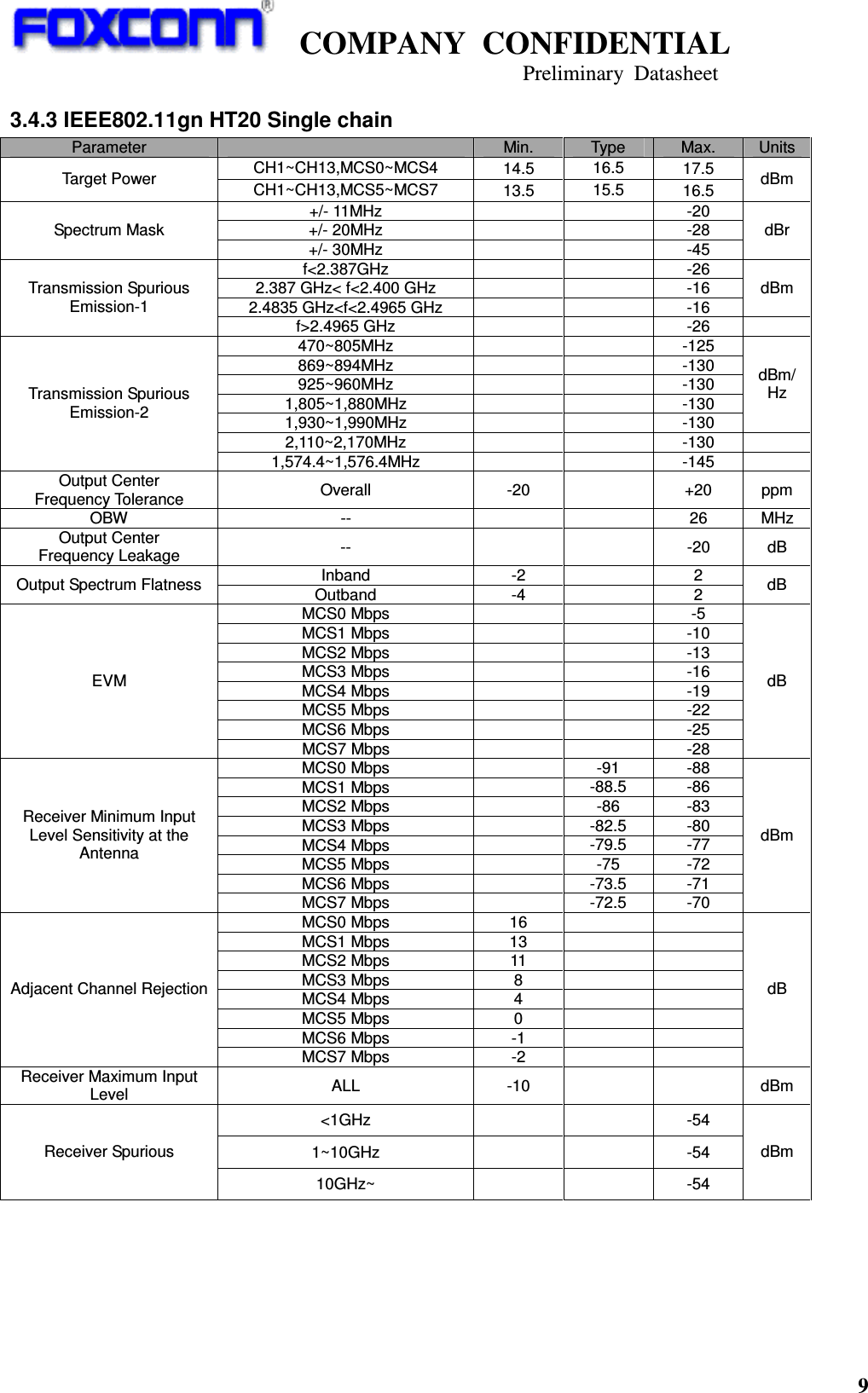
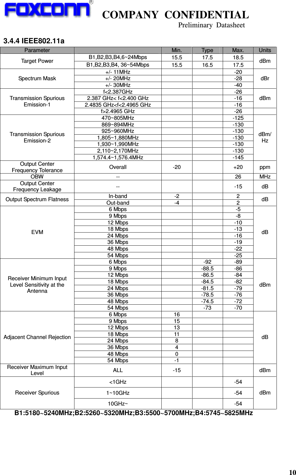
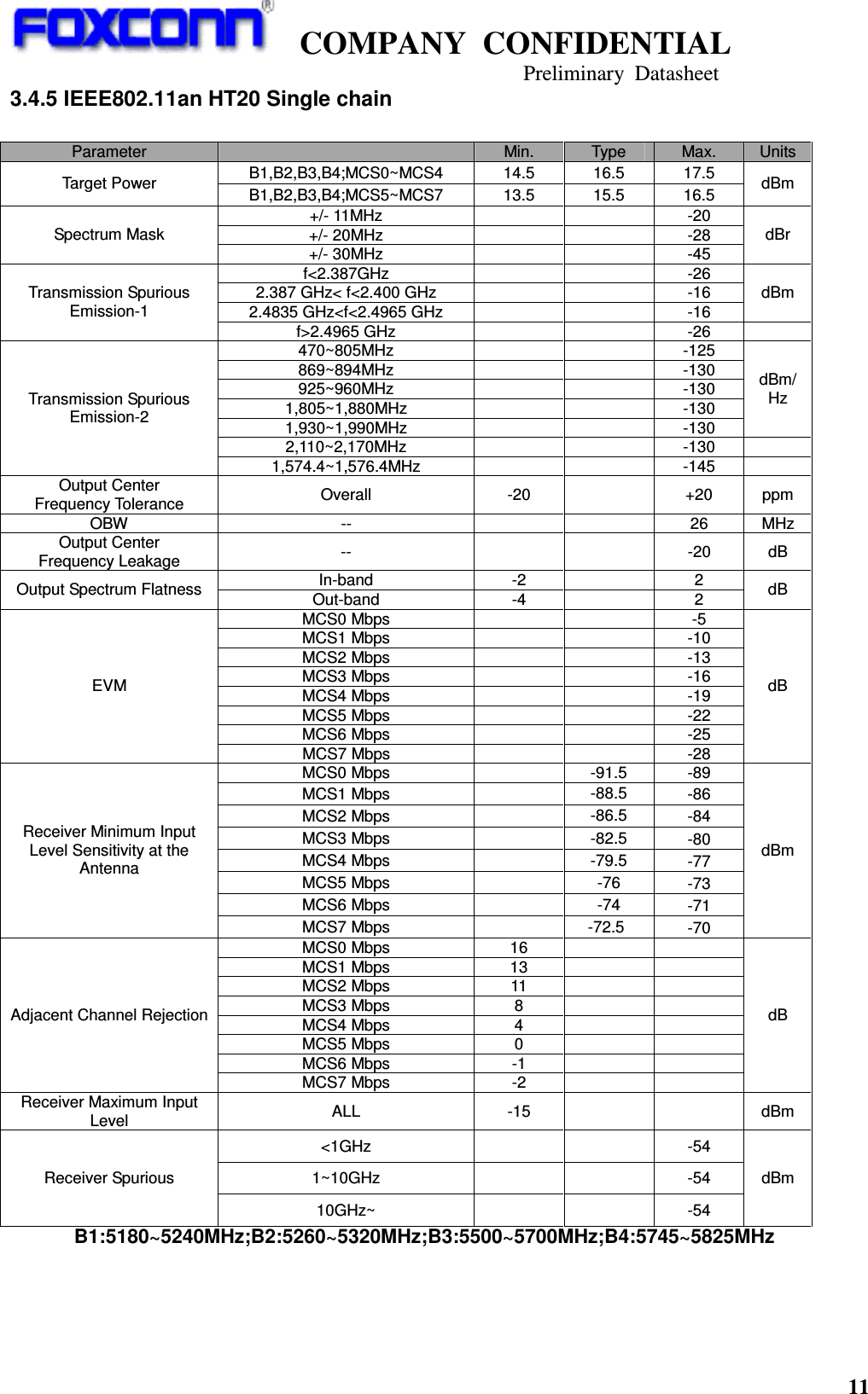
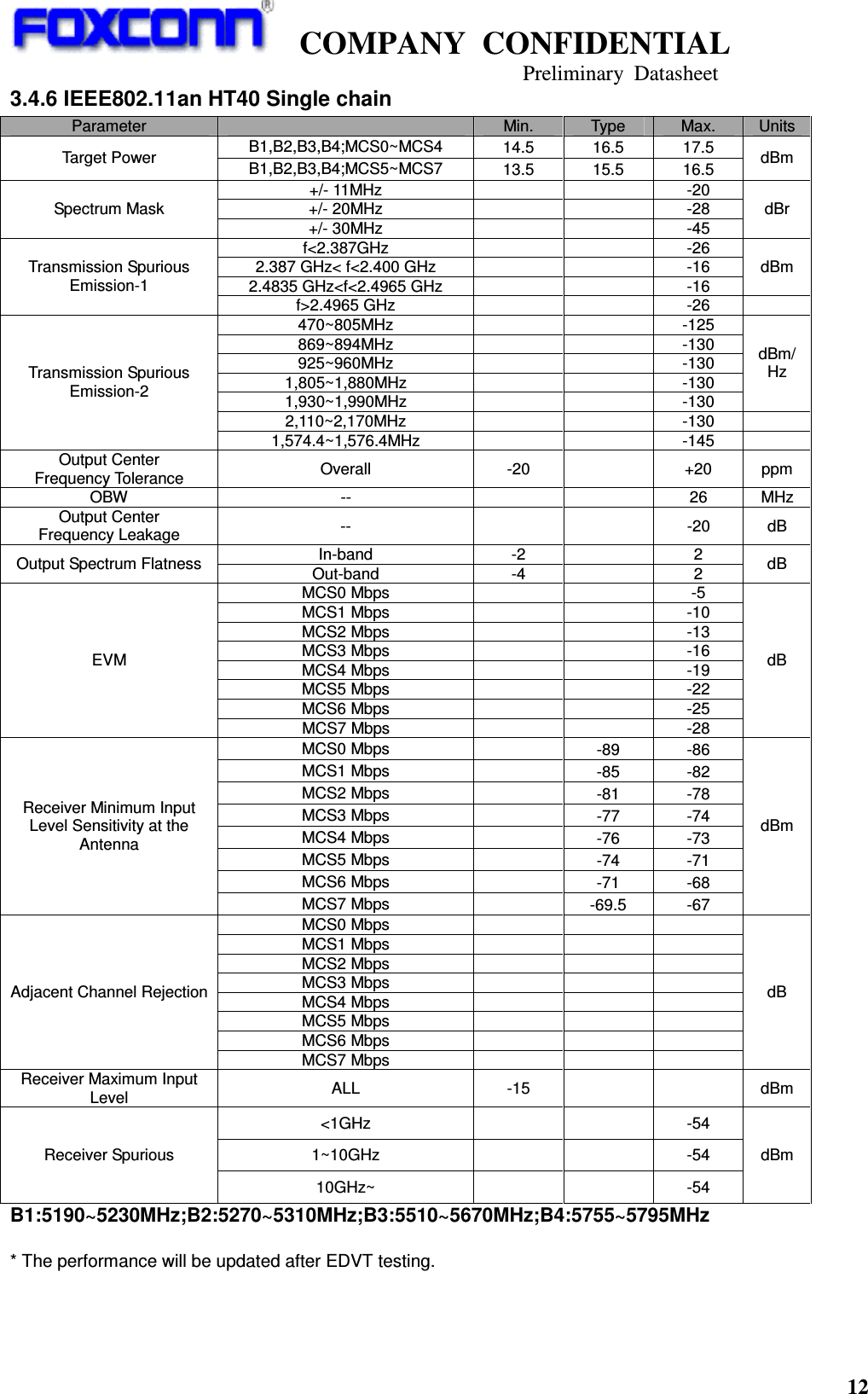
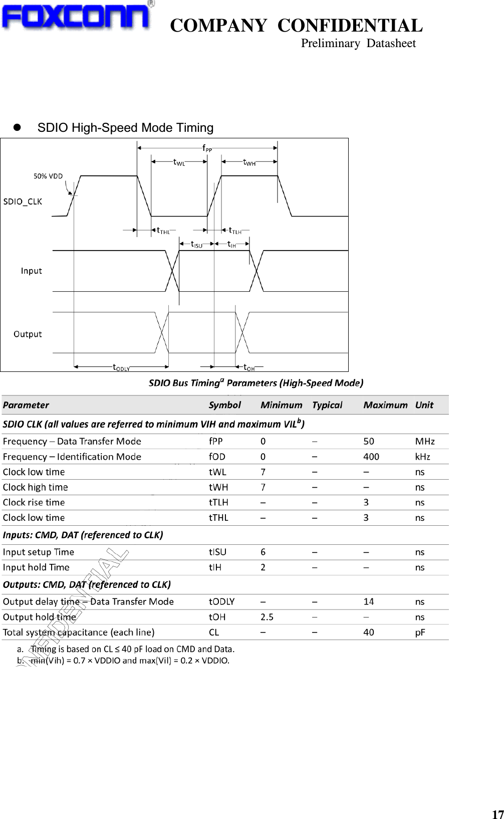
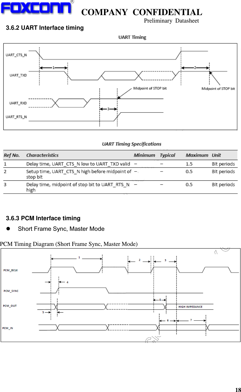
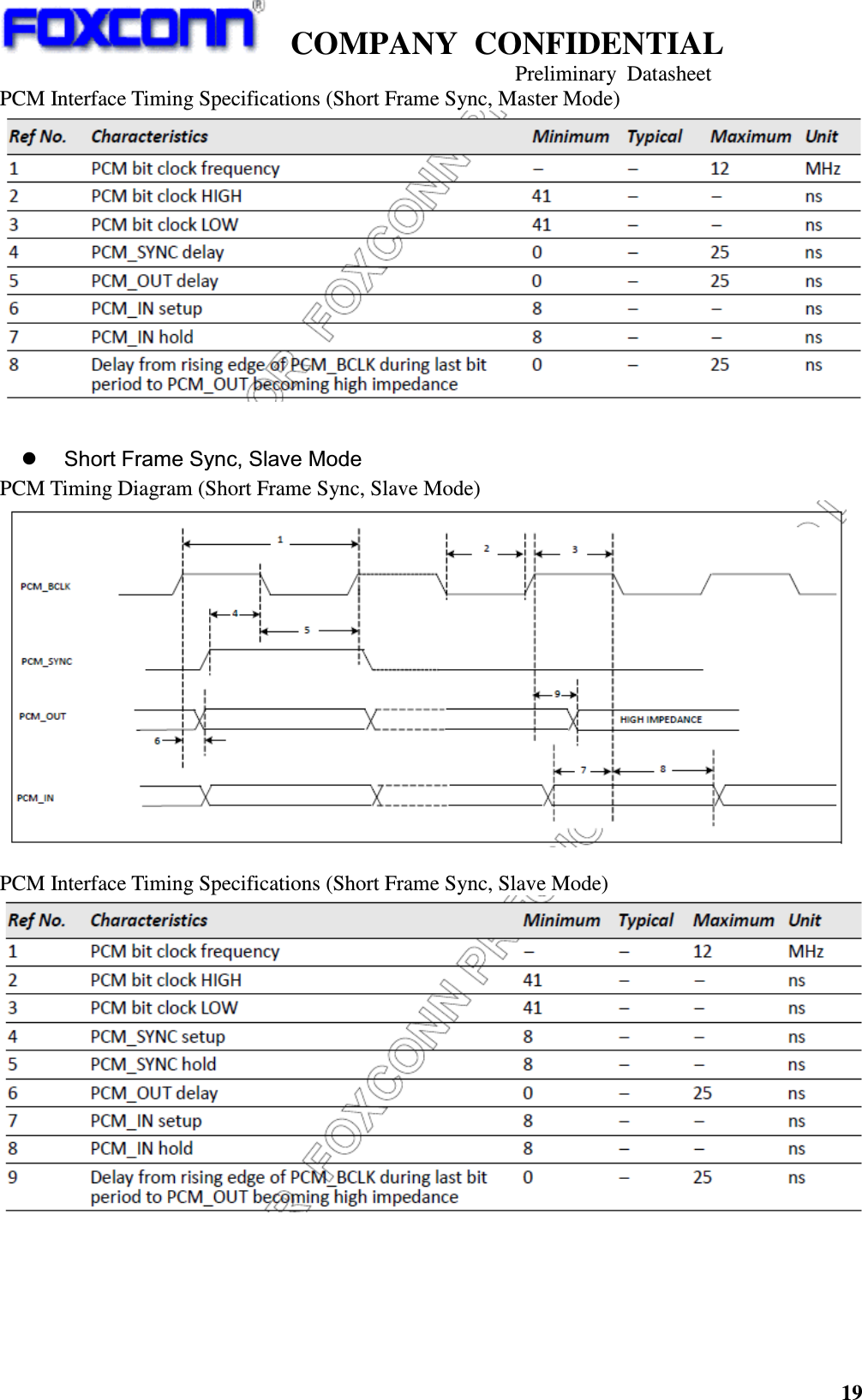
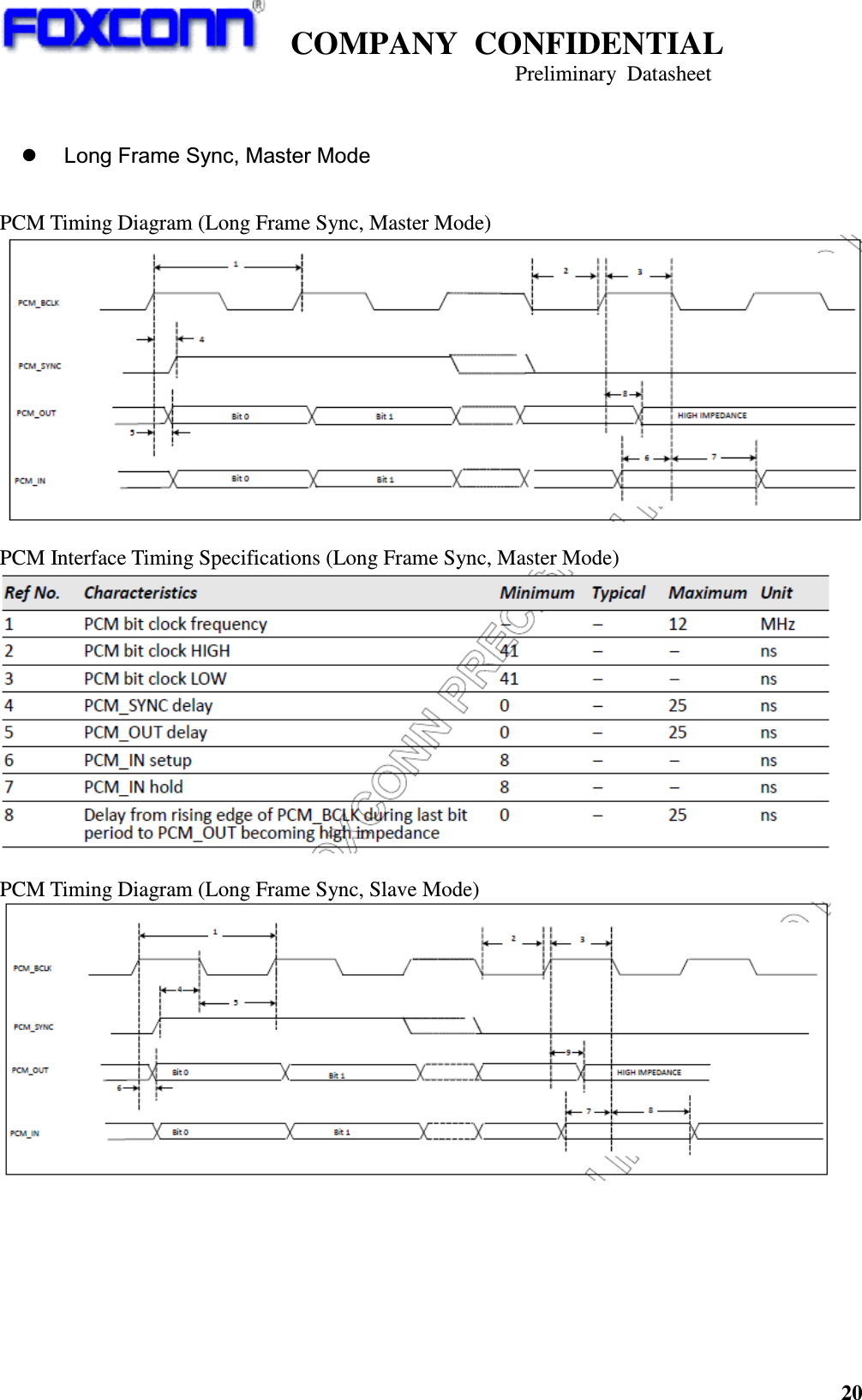
HON HAI PRECISION IND
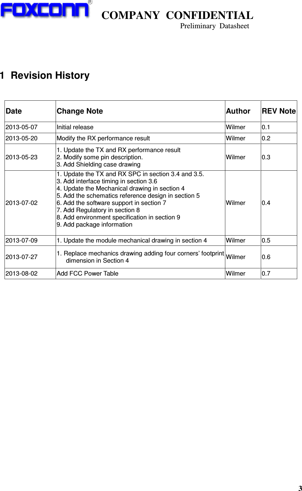
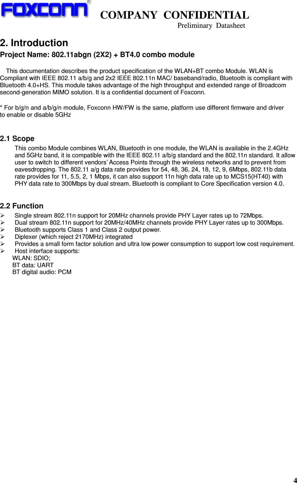
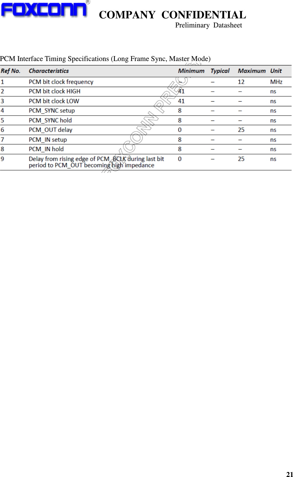
 T77H506 802.11abgn+BT4.0 module User Manual

HON HAI Precision Ind. Co., Ltd. 802.11abgn+BT4.0 module

User Manual.pdf

   COMPANY  CONFIDENTIAL                                                                     Preliminary  Datasheet 1             BCM4324 WLAN +BT Combo Module (Foxconn T77H506.00 035) Product Specification                                                     Rev 0.7                       Prepared by  Reviewed by  Approved by             Wilmer                Gary Su      Chang Fu
   COMPANY  CONFIDENTIAL                                                                     Preliminary  Datasheet 2                            Index 1. REVISION HISTORY...................................................................................................................................................3 2. INTRODUCTION ..........................................................................................................................................................4 2.1 SCOPE......................................................................................................................................................................4 2.2 FUNCTION.................................................................................................................................................................4 3. PRODUCT SPECIFICATION .....................................................................................................................................5 3.1 HARDWARE CHARACTERISTIC.................................................................................................................................5 3.2 HARDWARE ARCHITECTURE....................................................................................................................................5 3.3 ELECTRICAL SPECIFICATION....................................................................................................................................6 3.4 WLAN RF CHARACTERISTICS.................................................................................................................................7 3.4.1 IEEE802.11b ..................................................................................................................................................7 3.4.2 IEEE802.11g (SISO).....................................................................................................................................7 3.4.3 IEEE802.11gn HT20 Single chain ............................................................................................................9 3.4.4 IEEE802.11a ................................................................................................................................................10 3.4.5 IEEE802.11an HT20 Single chain ..........................................................................................................11 3.4.6 IEEE802.11an HT40 Single chain ..........................................................................................................12 3.5 BLUETOOTH STANDARD SPECIFICATIONS.............................................................................................................13 3.6 INTERFACE TIMING..................................................................................................................................................16 3.6.1 SDIO INTERFACE TIMING....................................................................................................................................16 3.6.2 UART INTERFACE TIMING...................................................................................................................................18 3.6.3 PCM INTERFACE TIMING.....................................................................................................................................18 4. MECHANICAL DRAWING .......................................................................................................................................25 5. SCHEMATIC REFERENCE DESIGN .....................................................................................................................28 6. PCB LAYOUT.............................................................................................................................................................30 7. SOFTWARE REQUIREMENT..................................................................................................................................30 8. REGULATORY...........................................................................................................................................................32 9. PACKAGE RELIABILITY TEST CONDITIONS ....................................................................................................33 10. ENVIRONMENTAL REQUIREMENTS AND SPECIFICATIONS.....................................................................33 10.1 TEMPERATURE.....................................................................................................................................................33 10.2 PCB BENDING......................................................................................................................................................33 10.3 HANDLING ENVIRONMENT....................................................................................................................................33 10.4 STORAGE CONDITION..........................................................................................................................................33 10.5 BAKING CONDITION..............................................................................................................................................34 10.6 SOLDERING AND REFLOW CONDITION..................................................................................................................34 11 PACKAGE INFORMATION.....................................................................................................................................34
   COMPANY  CONFIDENTIAL                                                                     Preliminary  Datasheet 3      1  Revision History   Date  Change Note  Author  REV Note 2013-05-07  Initial release  Wilmer  0.1 2013-05-20  Modify the RX performance result  Wilmer  0.2 2013-05-23 1. Update the TX and RX performance result 2. Modify some pin description. 3. Add Shielding case drawing Wilmer  0.3 2013-07-02 1. Update the TX and RX SPC in section 3.4 and 3.5. 3. Add interface timing in section 3.6 4. Update the Mechanical drawing in section 4 5. Add the schematics reference design in section 5 6. Add the software support in section 7 7. Add Regulatory in section 8 8. Add environment specification in section 9 9. Add package information  Wilmer  0.4 2013-07-09  1. Update the module mechanical drawing in section 4  Wilmer  0.5 2013-07-27  1. Replace mechanics drawing adding four corners’ footprint dimension in Section 4  Wilmer  0.6 2013-08-02  Add FCC Power Table  Wilmer  0.7
   COMPANY  CONFIDENTIAL                                                                     Preliminary  Datasheet 4  2. Introduction Project Name: 802.11abgn (2X2) + BT4.0 combo module  This documentation describes the product specification of the WLAN+BT combo Module. WLAN is Compliant with IEEE 802.11 a/b/g and 2x2 IEEE 802.11n MAC/ baseband/radio, Bluetooth is compliant with Bluetooth 4.0+HS. This module takes advantage of the high throughput and extended range of Broadcom second-generation MIMO solution. It is a confidential document of Foxconn.  * For b/g/n and a/b/g/n module, Foxconn HW/FW is the same, platform use different firmware and driver to enable or disable 5GHz  2.1 Scope This combo Module combines WLAN, Bluetooth in one module, the WLAN is available in the 2.4GHz and 5GHz band, it is compatible with the IEEE 802.11 a/b/g standard and the 802.11n standard. It allow user to switch to different vendors’ Access Points through the wireless networks and to prevent from eavesdropping. The 802.11 a/g data rate provides for 54, 48, 36, 24, 18, 12, 9, 6Mbps, 802.11b data rate provides for 11, 5.5, 2, 1 Mbps, it can also support 11n high data rate up to MCS15(HT40) with PHY data rate to 300Mbps by dual stream. Bluetooth is compliant to Core Specification version 4.0.  2.2 Function     Single stream 802.11n support for 20MHz channels provide PHY Layer rates up to 72Mbps.   Dual stream 802.11n support for 20MHz/40MHz channels provide PHY Layer rates up to 300Mbps.   Bluetooth supports Class 1 and Class 2 output power.   Diplexer (which reject 2170MHz) integrated   Provides a small form factor solution and ultra low power consumption to support low cost requirement.   Host interface supports: WLAN: SDIO;         BT data: UART         BT digital audio: PCM
   COMPANY  CONFIDENTIAL                                                                     Preliminary  Datasheet 5    3. Product Specification  3.1 Hardware Characteristic      Form factor                                            13mmx17mmx1.5mm LGA Host Interface                                        WLAN: SDIO                                                                 BT: UART for data, PCM for Audio       PCB                      6-layer HDI design RF connector  Two MHF4 RF connector on module  3.2 Hardware Architecture The  WLAN+BT  combo  module  is  designed  base  on  BROADCOM  BCM4324  chip,  the  Broadcom BCM4324 is a highly integrated single chip solution for single and dual stream dual-band WLAN and BT4.0. Single and dual Antenna support, a 37.4MHz crystal is used for reference clock generation, see the block diagram as below:
   COMPANY  CONFIDENTIAL                                                                     Preliminary  Datasheet 6   3.3 Electrical Specification Absolute Maximum Ratings These specifications indicate levels where permanent damage to the device can occur. Functional operation is not guaranteed under these conditions. Operation at absolute maximum conditions for extended can adversely affect long-term reliability of the device.   Recommended Operating Condition                             Value Element  Symbol Minimum    Typical  Maximum Unit DC supply voltage for the device  3.3V  3.0  3.3  3.6  V            Function operation is not guaranteed outside this limit, and operation outside this limit for extended periods can adversely affect long-term reliability of the device.    Power-Up Sequence Timing            Rating  Symbol  Value  Unit DC supply voltage for the device  3.3V  2.3 to 4.8  V
   COMPANY  CONFIDENTIAL                                                                     Preliminary  Datasheet 7    Current Consumption * Note: it would be updated after EDVT testing.  3.4 WLAN RF Characteristics 3.4.1 IEEE802.11b  Parameter  Condition  Min.  Type  Max.  Units Target Power  CH1~CH13, 1~11Mbps  16.5  18.5  19.5  dBm fc-22MHz<f< fc-11MHz fc+11MHz<f<fc+22MHz      -30 Spectrum Mask  f<fc-22MHz f>fc+22MHz      -50 dBr f<2.387GHz      -26 2.387 GHz< f<2.400 GHz      -16 2.4835 GHz<f<2.4965 GHz      -16 Transmission Spurious Emission-1 f>2.4965 GHz      -26 dBm 470~805MHz      -125 869~894MHz      -130 925~960MHz      -130 1,805~1,880MHz      -130 1,930~1,990MHz      -130 2,110~2,170MHz      -130 Transmission Spurious Emission-2 1,574.4~1,576.4MHz      -145 dBm/Hz OBW  --      26 Spread Bandwidth  --  7      MHz RF Carrier Suppression  Data=0101 and DQPSK modulation  15      dB Transmit power –on ramp  10% to 90% of max power      2  us Transmit power –down ramp  90% to 10% of max power      2  us Center Frequency Tolerance   -20    20  ppm 1Mbps      35 2Mbps      35 5.5Mbps      35 EVM (peak) 11Mbps      35 % 1 Mbps    -97  -94 2 Mbps    -94.5  -92 5.5 Mbps    -92.5  -90 Receiver Minimum Input Level Sensitivity at Antenna 11 Mbps    -89  -86 dBm Adjacent Channel Rejection  11Mbps  35      dB Receiver Maximum Input Level  ALL  0      dBm   3.4.2 IEEE802.11g (SISO) Parameter    Min.  Type  Max.  Units CH1~CH13,6~24Mbps  15  17 18 Target Power  CH1~CH13, 36~54Mbps  14  16  17  dBm Spectrum Mask  +/- 11MHz      -20  dBr
   COMPANY  CONFIDENTIAL                                                                     Preliminary  Datasheet 8  +/- 20MHz      -28 +/- 30MHz      -40 f<2.387GHz      -26 2.387 GHz< f<2.400 GHz      -16 2.4835 GHz<f<2.4965 GHz      -16 dBm Transmission Spurious Emission-1 f>2.4965 GHz      -26   470~805MHz      -125 869~894MHz      -130 925~960MHz      -130 1,805~1,880MHz      -130 1,930~1,990MHz      -130 2,110~2,170MHz      -130 Transmission Spurious Emission-2 1,574.4~1,576.4MHz      -145 dBm/ Hz Output Center Frequency Tolerance  Overall  -20    +20  ppm OBW  --      26  MHz Output Center Frequency Leakage  --      -15  dB In-band  -2    2 Output Spectrum Flatness  Out-band  -4    2  dB 6 Mbps      -5 9 Mbps      -8 12 Mbps      -10 18 Mbps      -13 24 Mbps      -16 36 Mbps      -19 48 Mbps      -22 EVM 54 Mbps      -25 dB 6 Mbps    -93  -90 9 Mbps    -91  -88 12 Mbps    -89.5  -87 18 Mbps    -87.5  -85 24 Mbps    -83.5  -81 36 Mbps    -81  -78 48 Mbps    -75.5  -73 Receiver Minimum Input Level Sensitivity at the Antenna 54 Mbps    -74.5  -72 dBm 6 Mbps  16     9 Mbps  15     12 Mbps  13     18 Mbps  11     24 Mbps  8     36 Mbps  4     48 Mbps  0     Adjacent Channel Rejection 54 Mbps  -1     dB Receiver Maximum Input Level  ALL  -10      dBm <1GHz      -54 1~10GHz      -54 Receiver Spurious 10GHz~      -54 dBm
   COMPANY  CONFIDENTIAL                                                                     Preliminary  Datasheet 9  3.4.3 IEEE802.11gn HT20 Single chain   Parameter    Min.  Type  Max.  Units CH1~CH13,MCS0~MCS4  14.5  16.5 17.5 Target Power  CH1~CH13,MCS5~MCS7  13.5  15.5 16.5  dBm +/- 11MHz      -20 +/- 20MHz      -28 Spectrum Mask +/- 30MHz      -45 dBr f<2.387GHz      -26 2.387 GHz< f<2.400 GHz      -16 2.4835 GHz<f<2.4965 GHz      -16 dBm Transmission Spurious Emission-1 f>2.4965 GHz      -26   470~805MHz      -125 869~894MHz      -130 925~960MHz      -130 1,805~1,880MHz      -130 1,930~1,990MHz      -130 dBm/ Hz 2,110~2,170MHz      -130   Transmission Spurious Emission-2 1,574.4~1,576.4MHz      -145   Output Center Frequency Tolerance  Overall  -20    +20  ppm OBW  --      26  MHz Output Center Frequency Leakage  --      -20  dB Inband  -2    2 Output Spectrum Flatness  Outband  -4    2  dB MCS0 Mbps     -5 MCS1 Mbps     -10 MCS2 Mbps     -13 MCS3 Mbps     -16 MCS4 Mbps     -19 MCS5 Mbps     -22 MCS6 Mbps     -25 EVM MCS7 Mbps     -28 dB MCS0 Mbps  -91  -88 MCS1 Mbps  -88.5  -86 MCS2 Mbps  -86  -83 MCS3 Mbps  -82.5  -80 MCS4 Mbps  -79.5  -77 MCS5 Mbps  -75  -72 MCS6 Mbps  -73.5  -71 Receiver Minimum Input Level Sensitivity at the Antenna MCS7 Mbps  -72.5  -70 dBm MCS0 Mbps 16     MCS1 Mbps 13     MCS2 Mbps 11     MCS3 Mbps 8     MCS4 Mbps 4     MCS5 Mbps 0     MCS6 Mbps -1     Adjacent Channel Rejection MCS7 Mbps -2     dB Receiver Maximum Input Level  ALL  -10      dBm <1GHz      -54 1~10GHz      -54 Receiver Spurious 10GHz~      -54 dBm
   COMPANY  CONFIDENTIAL                                                                     Preliminary  Datasheet 10  3.4.4 IEEE802.11a Parameter    Min.  Type  Max.  Units B1,B2,B3,B4,6~24Mbps  15.5  17.5  18.5 Target Power  B1,B2,B3,B4, 36~54Mbps  15.5  16.5  17.5  dBm +/- 11MHz      -20 +/- 20MHz      -28 Spectrum Mask +/- 30MHz      -40 dBr f<2.387GHz      -26 2.387 GHz< f<2.400 GHz      -16 2.4835 GHz<f<2.4965 GHz      -16 dBm Transmission Spurious Emission-1 f>2.4965 GHz      -26   470~805MHz      -125 869~894MHz      -130 925~960MHz      -130 1,805~1,880MHz      -130 1,930~1,990MHz      -130 2,110~2,170MHz      -130 Transmission Spurious Emission-2 1,574.4~1,576.4MHz      -145 dBm/ Hz Output Center Frequency Tolerance  Overall  -20    +20  ppm OBW  --      26  MHz Output Center Frequency Leakage  --      -15  dB In-band  -2    2 Output Spectrum Flatness  Out-band  -4    2  dB 6 Mbps      -5 9 Mbps      -8 12 Mbps      -10 18 Mbps      -13 24 Mbps      -16 36 Mbps      -19 48 Mbps      -22 EVM 54 Mbps      -25 dB 6 Mbps    -92  -89 9 Mbps    -88.5  -86 12 Mbps    -86.5  -84 18 Mbps    -84.5  -82 24 Mbps    -81.5  -79 36 Mbps    -78.5  -76 48 Mbps    -74.5  -72 Receiver Minimum Input Level Sensitivity at the Antenna 54 Mbps    -73  -70 dBm 6 Mbps  16     9 Mbps  15     12 Mbps  13     18 Mbps  11     24 Mbps  8     36 Mbps  4     48 Mbps  0     Adjacent Channel Rejection 54 Mbps  -1     dB Receiver Maximum Input Level  ALL  -15      dBm <1GHz      -54 1~10GHz      -54 Receiver Spurious 10GHz~      -54 dBm B1:5180~5240MHz;B2:5260~5320MHz;B3:5500~5700MHz;B4:5745~5825MHz
   COMPANY  CONFIDENTIAL                                                                     Preliminary  Datasheet 11  3.4.5 IEEE802.11an HT20 Single chain      Parameter    Min.  Type  Max.  Units B1,B2,B3,B4;MCS0~MCS4  14.5  16.5  17.5 Target Power  B1,B2,B3,B4;MCS5~MCS7  13.5  15.5  16.5  dBm +/- 11MHz      -20 +/- 20MHz      -28 Spectrum Mask +/- 30MHz      -45 dBr f<2.387GHz      -26 2.387 GHz< f<2.400 GHz      -16 2.4835 GHz<f<2.4965 GHz      -16 dBm Transmission Spurious Emission-1 f>2.4965 GHz      -26   470~805MHz      -125 869~894MHz      -130 925~960MHz      -130 1,805~1,880MHz      -130 1,930~1,990MHz      -130 dBm/ Hz 2,110~2,170MHz      -130   Transmission Spurious Emission-2 1,574.4~1,576.4MHz      -145   Output Center Frequency Tolerance  Overall  -20    +20  ppm OBW  --      26  MHz Output Center Frequency Leakage  --      -20  dB In-band  -2    2 Output Spectrum Flatness  Out-band  -4    2  dB MCS0 Mbps     -5 MCS1 Mbps     -10 MCS2 Mbps     -13 MCS3 Mbps     -16 MCS4 Mbps     -19 MCS5 Mbps     -22 MCS6 Mbps     -25 EVM MCS7 Mbps     -28 dB MCS0 Mbps  -91.5  -89 MCS1 Mbps  -88.5  -86 MCS2 Mbps  -86.5  -84 MCS3 Mbps  -82.5  -80 MCS4 Mbps  -79.5  -77 MCS5 Mbps  -76  -73 MCS6 Mbps  -74  -71 Receiver Minimum Input Level Sensitivity at the Antenna MCS7 Mbps     -72.5  -70 dBm MCS0 Mbps 16     MCS1 Mbps 13     MCS2 Mbps 11     MCS3 Mbps 8     MCS4 Mbps 4     MCS5 Mbps 0     MCS6 Mbps -1     Adjacent Channel Rejection MCS7 Mbps -2     dB Receiver Maximum Input Level  ALL  -15      dBm <1GHz      -54 1~10GHz      -54 Receiver Spurious 10GHz~      -54 dBm    B1:5180~5240MHz;B2:5260~5320MHz;B3:5500~5700MHz;B4:5745~5825MHz
   COMPANY  CONFIDENTIAL                                                                     Preliminary  Datasheet 12  3.4.6 IEEE802.11an HT40 Single chain Parameter    Min.  Type  Max.  Units B1,B2,B3,B4;MCS0~MCS4  14.5  16.5  17.5 Target Power  B1,B2,B3,B4;MCS5~MCS7  13.5  15.5  16.5  dBm +/- 11MHz      -20 +/- 20MHz      -28 Spectrum Mask +/- 30MHz      -45 dBr f<2.387GHz      -26 2.387 GHz< f<2.400 GHz      -16 2.4835 GHz<f<2.4965 GHz      -16 dBm Transmission Spurious Emission-1 f>2.4965 GHz      -26   470~805MHz      -125 869~894MHz      -130 925~960MHz      -130 1,805~1,880MHz      -130 1,930~1,990MHz      -130 dBm/ Hz 2,110~2,170MHz      -130   Transmission Spurious Emission-2 1,574.4~1,576.4MHz      -145   Output Center Frequency Tolerance  Overall  -20    +20  ppm OBW  --      26  MHz Output Center Frequency Leakage  --      -20  dB In-band  -2    2 Output Spectrum Flatness  Out-band  -4    2  dB MCS0 Mbps     -5 MCS1 Mbps     -10 MCS2 Mbps     -13 MCS3 Mbps     -16 MCS4 Mbps     -19 MCS5 Mbps     -22 MCS6 Mbps     -25 EVM MCS7 Mbps     -28 dB MCS0 Mbps  -89  -86 MCS1 Mbps  -85  -82 MCS2 Mbps  -81  -78 MCS3 Mbps  -77  -74 MCS4 Mbps  -76  -73 MCS5 Mbps  -74  -71 MCS6 Mbps  -71  -68 Receiver Minimum Input Level Sensitivity at the Antenna MCS7 Mbps  -69.5  -67 dBm MCS0 Mbps      MCS1 Mbps      MCS2 Mbps      MCS3 Mbps      MCS4 Mbps      MCS5 Mbps      MCS6 Mbps      Adjacent Channel Rejection MCS7 Mbps      dB Receiver Maximum Input Level  ALL  -15      dBm <1GHz      -54 1~10GHz      -54 Receiver Spurious 10GHz~      -54 dBm B1:5190~5230MHz;B2:5270~5310MHz;B3:5510~5670MHz;B4:5755~5795MHz  * The performance will be updated after EDVT testing.
   COMPANY  CONFIDENTIAL                                                                     Preliminary  Datasheet 13  3.5 Bluetooth Standard Specifications Bluetooth Core Specification version 4.0: Host interface: UART, baud rates up to 4Mbps Support all Bluetooth 4.0+HS packet types. Operating frequency range: 2400MHz ~2483.5MHz Modulation type:   Basic rate 1Mbps: GFSK, Enhanced data rate 2Mbps: QPSK Enhanced data rate 3Mbps: 8PSK Specification Parameter  Condition Min  Typ  Max Units Basic Data Rate – Transmit Performance RF Transmit Power at the Antenna  +5  +8  +11  dBm -20 dB Bandwidth    1 Tx Output Spectrum  Frequency range      83.5  MHz Initial Carrier Frequency Tolerance  ≤ ±75  KHz DH1/3/5 Drift rate  ≤ ±20  kHz/50 µs DH1  <±20 DH3  ≤ ±40 Carrier Frequency Drift DH5  <±40 KHz F1avg  140<∆f1avg<175 F2max  ≥ 115 kHz Modulation Characteristics F2avg/F1avg  80  % +/-500KHz    -27    dBc |M-N|=2      -20 Adjacent Channel Transmit Power  |M-N|≥3      -40  dBm f<2.387GHz      -26 2.387 GHz< f<2.400 GHz      -16 2.4835 GHz<f<2.4965 GHz      -16 dBm Transmission Spurious Emission-1 f>2.4965 GHz      -26   470~805MHz      -130 869~894MHz      -135 925~960MHz      -135 1,805~1,880MHz      -135 1,930~1,990MHz      -135 dBm/ Hz 2,110~2,170MHz      -135  Transmission Spurious Emission-2 1,574.4~1,576.4MHz      -150  Enhanced Data Rate – Transmit Performance π/4 DQPSK  +3  +6  +9 RF Transmit Power 8DPSK  +3  +6  +9 dBm Relative Transmit Power  Pdpsk  (PGFSK-4 dB)<PDPSK<(PGFSK+1 dB)  i  -75    75 0  -10    10 Carrier Frequency Stability i + 0  -75    75 kHz π/4 DQPSK  ≤ 20 Modulation Accuracy – RMS DEVM  8DPSK  ≤ 13 π/4 DQPSK  ≤ 35 Modulation Accuracy – Peak DEVM 8DPSK  ≤ 25 Modulation Accuracy – 99%  π/4 DQPSK  ≤ 30 %
   COMPANY  CONFIDENTIAL                                                                     Preliminary  Datasheet 14  DEVM  8DPSK  ≤ 20 f>f0+3 MHz  ≤ -40 f<f0-3 MHz  ≤ -40 f=f0-3 MHz  ≤ -40 f=f0-2 MHz  ≤ -20 dBm f=f0-1 MHz  ≤ -26 f=f0+1 MHz  ≤ -26 dBr f=f0+2 MHz  ≤ -20 In-band Spurious Emissions f=f0+3 MHz  ≤ -40 dBm EDR Differential Phase Coding  99      % f<2.387GHz      -26 2.387 GHz< f<2.400 GHz      -16 2.4835 GHz<f<2.4965 GHz      -16 dBm Transmission Spurious Emission-1 f>2.4965 GHz      -26   470~805MHz      -130 869~894MHz      -135 925~960MHz      -135 1,805~1,880MHz      -135 1,930~1,990MHz      -135 dBm/ Hz 2,110~2,170MHz      -135  Transmission Spurious Emission-2 1,574.4~1,576.4MHz      -150  Basic Data Rate – Receiver Performance at the Antenna Sensitivity (DH1) at 0.1% BER  Nominal      -86  dBm Co-ch interface C/Ico  <11 Adjacent Chanel Sensitivity C/I f=f0±1 MHz  < 0 Adjacent Chanel Sensitivity C/I f=f0±2 MHz  <-30 Adjacent Chanel Sensitivity C/I f≥f0±3 MHz  < -40 Image Ch interference C/Iimage  < -9 C/I Performance at BER≤0.1% Image Ch interference C/Iimage1MHz < -20 dB 30MHz~2GHz  -10     2GHz~2.4GHz  -27     2.5GHz~3GHz  -27     Blocking Performance at BER≤0.1% 3GHz~12.75GHz  -10     dBm Intermodulation Performance at BER≤0.1%  Carrier Level:-64dBm  -39      dBm Max input Level    -20      dBm <1GHz      -54 1~10GHz      -54 Receiver Spurious 10GHz~      -54 dBm Enhanced Data Rate – Receiver Performance at the Antenna Sensitivity at  Nominal π/4 DQPSK(ch0~78)      -88  dBm
   COMPANY  CONFIDENTIAL                                                                     Preliminary  Datasheet 15  8DPSK(ch0~78)      -85 BER≤0.01%  π/4 DQPSK  -20     Max input Level 8DPSK  -20     dBm Co-ch interface C/Ico  <13 Adjacent Chanel Sensitivity C/I f=f0±1 MHz  < 0 Adjacent Chanel Sensitivity C/I f=f0±2 MHz  <-30 Adjacent Chanel Sensitivity C/I f≥f0±3 MHz  < -40 Image Ch interference C/Iimage  < -7 C/I Performance at BER≤0.1%(π/4 DQPSK) Image Ch interference C/Iimage1MHz < -20 dB Co-ch interface C/Ico  <21 Adjacent Chanel Sensitivity C/I f=f0±1 MHz  < 5 Adjacent Chanel Sensitivity C/I f=f0±2 MHz  <-25 Adjacent Chanel Sensitivity C/I f≥f0±3 MHz  < -33 Image Ch interference C/Iimage  < -0 C/I Performance at BER≤0.1%(8DPSK) Image Ch interference C/Iimage1MHz < -13 dB <1GHz      -54 1~10GHz      -54 Receiver Spurious 10GHz~      -54 dBm  BLE RF specification:  BLE RF specification: Sensitivity at BER≤0.01%  Nominal GFSK 0.1%, 1M   TBD -85.5 dBm RF Transmit Power  GFSK  1  TBD 8  dBm Mod char:delta f1 average    225   275  kHz Mod char:delta f2 max    99.9     % <1GHz      -54 1~10GHz      -54 Receiver Spurious 10GHz~      -54 dBm f<2.387GHz      -26 2.387 GHz< f<2.400 GHz      -16 2.4835 GHz<f<2.4965 GHz      -16 dBm Transmission Spurious Emission-1 f>2.4965 GHz      -26   470~805MHz      -130 869~894MHz      -135 925~960MHz      -135 1,805~1,880MHz      -135 1,930~1,990MHz      -135 dBm/ Hz 2,110~2,170MHz      -135  Transmission Spurious Emission-2 1,574.4~1,576.4MHz      -150
   COMPANY  CONFIDENTIAL                                                                     Preliminary  Datasheet 16  3.6 Interface timing 3.6.1 SDIO Interface timing  SDIO Default Mode timing
   COMPANY  CONFIDENTIAL                                                                     Preliminary  Datasheet 17      SDIO High-Speed Mode Timing
   COMPANY  CONFIDENTIAL                                                                     Preliminary  Datasheet 18  3.6.2 UART Interface timing   3.6.3 PCM Interface timing  Short Frame Sync, Master Mode  PCM Timing Diagram (Short Frame Sync, Master Mode)
   COMPANY  CONFIDENTIAL                                                                     Preliminary  Datasheet 19  PCM Interface Timing Specifications (Short Frame Sync, Master Mode)    Short Frame Sync, Slave Mode PCM Timing Diagram (Short Frame Sync, Slave Mode)                                                       PCM Interface Timing Specifications (Short Frame Sync, Slave Mode)
   COMPANY  CONFIDENTIAL                                                                     Preliminary  Datasheet 20     Long Frame Sync, Master Mode  PCM Timing Diagram (Long Frame Sync, Master Mode)   PCM Interface Timing Specifications (Long Frame Sync, Master Mode)   PCM Timing Diagram (Long Frame Sync, Slave Mode)
   COMPANY  CONFIDENTIAL                                                                     Preliminary  Datasheet 21     PCM Interface Timing Specifications (Long Frame Sync, Master Mode)
   COMPANY  CONFIDENTIAL                                                                     Preliminary  Datasheet 22  3.7 LGA Pin Definition - Module pin-out definition:    - Platform pin-out definition:
   COMPANY  CONFIDENTIAL                                                                     Preliminary  Datasheet 23  -  Pin definition (Module point of view):  Pin No. Pin Name  Type  Description  Voltage 1-3  UIM_power_in/GPIO1 UIM_power_out UIM_SWP I/O  No connection  - 4-5  3.3V  Power  Power voltage input pin  3.3V 6  GND  GND  Ground  - 7  Reserved  I/O  Reserved LGA pin  - 8*(a)  ALERT  -  No connection -  9*(a)  I2C CLK  -  No connection -  10*(a)  I2C DATA  -  No connection - 11*(a)  COEX1  -  No connection - 12*(a)  COEX2  -  No connection - 13*(a)  COEX3  -  No connection - 14-15  SYSCLK/GNSS0 TX_Blanking/GNSS1 -  Reserved LGA pin, No connection    16  Reserved  I/O  Reserved LGA pin, No connection   17  GND  GND  Ground   18-19  Reserved  -  Reserved LGA pin, No connection   20  GND  GND  Ground   21-22  Reserved  -  Reserved LGA pin, No connection   23  GND  GND  Ground   24-25  Reserved  -  Reserved LGA pin, No connection   26  GND  GND  Ground   27  SUSCLK (32KHz)  I  32.768 kHz clock supply input that is provided by PCH to reduce power and cost for the module. SUSCLK will have a duty cycle that can be as low as 30% or as high as 70%. 200ppm.   3.3V 28    W_DISABLE#1  I  No connection   29*(a)  PEWAKE#  -  No connection - 30*(a)  CLKREQ#  -  No connection - 31*(a)  PERST#  -  No connection - 32  GND  GND  Ground   33*(a)  REFCLKN0 34*(a)  REFCLKP0 -  No connection - 35  GND  GND  Ground   36*(a)  PETn0 37*(a)  PETp0 -  No connection - 38  GND  GND  Ground   39*(a)  PERn0 40*(a)  PERp0 -  No connection - 41  GND  GND  Ground   42-44  Reserved  -  Reserved LGA pin, No connection   45  SDIO Reset  I SDIO sideband GPIO pin to enable/disable (reset) the WiFi function. Platform firmware is required to assert/de-assert this pin on every boot (warm and cold). The WiFi device may use 0.5 to 1 mW in reset, Active Low   1.8V 46  SDIO Wake  O  SDIO Host Wake. Note in band SDIO wake is not used for non-active modes, Active Low. Require pull up on the host side ( recommended 15K to 100K )   1.8V 47  SDIO DATA3  I/O  4 lines for SDIO data exchange    1.8V 48  SDIO DATA2  I/O  4 lines for SDIO data exchange    1.8V
   COMPANY  CONFIDENTIAL                                                                     Preliminary  Datasheet 24  49  SDIO DATA1  I/O  4 lines for SDIO data exchange    1.8V 50  SDIO DATA0  I/O  4 lines for SDIO data exchange    1.8V 51  SDIO CMD  I/O  SDIO Command Interface  1.8V 52  SDIO CLK  I  SDIO 3.0 Clock    1.8V 53  UART WAKE  O  Bluetooth host Wake. Active Low    3.3V 54  UART CTS  I  UART Clear To Send, Active low, connected to UART RTS on the platform. 1.8V 55  UART TX  O  UART Transmit Data, connected to UART RX on the platform. 1.8V 56  UART RX  I  UART Receive Data, connected to UART TX on the platform. 1.8V 58  UART RTS  O  UART Request To Send, Active low, connected to UART CTS on the platform. 1.8V 58  PCM FR1  I/O  PCM Synchronous data sync/ I2S Word Select    1.8V 59  PCMIN  I  PCM Synchronous data input/ I2S Serial Data IN  1.8V 60  PCMOUT  O  PCM Synchronous data output/ I2S Serial Data OUT 1.8V 61  PCMCLK  I/O  PCM Clock/ I2S Continuous Serial Clock (SCK)    1.8V 62  GND  GND  Ground   63  W_DISABLE#2  I  Active low, debounced signal when applied by the platform it will disable BT radio operation   3.3V 64  LED#2  -  No connection - 65  LED#1  -  No connection - 66-67  Reserved  -  Reserved LGA pin   68  GND  GND  Ground   69*(a)  USB_D- 70*(a)  USB _D+ -  No connection - 71  GND  GND  Ground   72-73  3.3V  Power  Power voltage input pin  3.3V 74-76, others GND  GND  Ground    The pin-out definition is following NGFF1216 standard, but removed partial functions such as PCIE, BT_USB. All of function used is following the BCM4324 application. *(a) FOXCONN remove the function according to BCM4324 function.
   COMPANY  CONFIDENTIAL                                                                     Preliminary  Datasheet 25  4. Mechanical Drawing  Foxconn can provide the DXF file for detail dimension as following drawing.   (Dimension Tolerance is +-0.15 mm)  Footprint (Top view)
   COMPANY  CONFIDENTIAL                                                                     Preliminary  Datasheet 26    T77H506.00 035 Shielding Cover    Antenna port location as following drawing ((Dimension Tolerance is +-0.15 mm))
   COMPANY  CONFIDENTIAL                                                                     Preliminary  Datasheet 27  RF connector:    - New RF connector is needed, for lower z-height and smaller footprint   - Same RF Receptacle on module supports either 0.81mm or 1.13mm diameter cable - Cable diameter determines mated height: 1.2mm mated height with 0.81mm cable  4.3 Example of IPEX RF connector IPEX P/N:    20449-001E (MHF4) IPEX P/N:    20448-001R-081
   COMPANY  CONFIDENTIAL                                                                     Preliminary  Datasheet 28   5. Schematic Reference Design Following is the Evaluation board schematics for reference.  Module pinout & 32.768kHz BT_UART_CTS_NBT_UART_RTS_NBT_UART_RXDBT_UART_TXDBT_PCM_INBT_PCM_OUTBT_REG_ONIRQ line to host processorVBAT 3.3VC1810uFC-080512C170.1uFC-0603S012C210uFC-080512R10ohmR-0603S012C31uFC-0603S012C410nFC-0402S012GPIO0_WL_HOST_WAKEWL_REG_ON3.3VY1XTAL-7B250000011234C1NLC-0402S012R2221ohmR-0402S012SDIO Trace impedance is 50ohm R3910KohmR-0603S0123.3V3.3VR4110KohmR-0603S012SDIO_D2SDIO_D3SDIO_CMDSDIO_D0SDIO_D1SDIO_CLKBT_PCM_SYNCT77H506.00Reserv ed15 43Reserved919Reserv ed14 42SDIO_DAT3 47GND663.3V143.3V25Reserved11Reserved22Reserved33I2C_DATA10COEX111ALERT8Reserved716GND1717Reserved818GND2323Reserved1224Reserv ed16 44W_DISABLE#128CLKREQ# 30PERST# 31REFCLKP0 34PEWAKE# 29SDIO_Reset 45Reserved47GND32 32SDIO_Wake 46SDIO_DAT2 48SDIO_DAT1 49SDIO_CMD 51SDIO_CLK 52I2C_CLK9GND2020Reserved1021Reserved1122GND35 35PETn0 36PETp0 37SDIO_DAT0 50REFCLKN0 33SUSCLK(32kHz)27GND2626Reserved1325COEX212COEX313Reserved514Reserved615GND38 38PERn0 39PERp0 40GND41 41UART_WAKE 53UART_CTS 54UART_Tx 55UART_Rx 56UART_RTS 57PCMFR1 58BT_PCMIN 59PCMOUT 60PCMCLK 61GND62 62W_DISABLE#2 63LED#2 64LED#1 65Reserved17 66Reserved18 67GND68 68USB_D- 69USB_D+ 70GND71 713.3V3 723.3V4 73GND74 74GND75 75GND76 76GND7777GNDG1G1GND7878GND7979GND8080GND8181GND8282GND8383GND8484GND8585GND8686GND8787GND8888GND8989GND9090GND9191GND9292GND9393GND9494GND9595GND9696GNDG2G2GNDG3G3GNDG4G4GNDG5G5GNDG6G6GNDG7G7GNDG8G8GNDG9G9GNDG10G10GNDG11G11GNDG12G12BT_PCM_CLKVBAT 3.3VC2310uFC-080512C240.1uFC-0603S012BT_HOST_WAKE 5-1  Low Power Clock The T77H506 module uses a secondary low frequency clock for low power mode timing. A precision external 32.768 KHz clock that meets the specifications listed in Table 3 is required by BCM4324.   Table 3: External 32.768K Low Power Oscillator Specifications  Specification Parameter Conditions/ Notes Min Typ Max Units Frequency   32748  32768  32788  Hz Input signal amplitude 25   200    1800  mV, p-p Duty cycle Square waveor  30  -  70  %
   COMPANY  CONFIDENTIAL                                                                     Preliminary  Datasheet 29  Specification sine- wave Clock jitter 300Hz-15KHz  -    5  ns Clock jitter During initial start-up     10,000  ppm C210uFC-080512R10ohmR-0603S012C31uFC-0603S012C410nFC-0402S0123.3VY1XTAL-7B250000011234C1NLC-0402S012R2221ohmR-0402S012 CLK32K (Pin27) 5-2  Audio PCM interface:
   COMPANY  CONFIDENTIAL                                                                     Preliminary  Datasheet 30  6. PCB Layout 6-layer, 2 order HDI FR-4 (Halogen Free) design, total thickness 0.3+/-0.03mm  7. Software Requirement - Operating System Support  Windows 8  Windows Blue or later Android 4.3 and above  - WLAN Feature Support  WiFi Direct  WiFi Display    Wi-Fi Miracast (Intel will support WiDi with Miracast interoperability)  - WLAN Security Support  WPA/WPA2 Enterprise  CCX Lite or higher  WMM/AES/TKIP/CKIP  - WLAN Transmit Power Reduction  Software control to meet FCC SAR requirement  Capability to disable 5GHz operation  - Bluetooth Profile Support  A2DP-Sink  A2DP-Source  AVRCP-Target  DUN-DT  FTP-Client  FTP-Server  HCRP-Client  HID-Host  MCAP  OPP-Client  OPP-Server  PAN-User
   COMPANY  CONFIDENTIAL                                                                     Preliminary  Datasheet 31   SDP  Serial-DevA  Serial-DevB  - BLE (Bluetooth Low Energy) Support  Windows 8  Windows Blue or later
   COMPANY  CONFIDENTIAL                                                                     Preliminary  Datasheet 32  8. Regulatory  USA : FCC P15B / FCC P15C / FCC P15E  Canada : IC RSS-210  Japan : TELEC  EU : EN300328 V1.8.1 , EN301893 V1.6.1 , EN301489-1/-17 , EN 60950-1 2nd   BCM4324 module 5GHz power table   Typical power (limit is +1/-2dB) (unit:dBm) HT20                          CH36      CH48      CH52      CH64      CH100      CH120      CH140      CH149      CH165 ANT0  16 16 17.5 17.5 17.5 17.5 17 17.5 17.5 6Mbps ANT1  16 16 17.5 17.5 17.5 17.5 17 17.5 17.5 MCS8 2Tx  16 16 19.5 19.5 19.5 19.5 19.5 19.5 19.5   HT40                         CH38    CH64      CH54      CH62      CH102      CH134      CH151      CH159 MCS8 2Tx  16 16 19.5 18 19 19.5 19.5 19.5   BCM4324 module 2.4GHz power table  Typical power (limit is +1/-2dB) (unit:dBm) HT20                      CH1        CH2      CH3      CH4      CH5      CH6      CH7      CH8      CH9      CH10        CH11 ANT0 15.5 15.5 15.5 15.5 15.5 15.5 15.5 15.5 15.5 15.5 15.5 1Mbps ANT1 18 18 18 18 18 18 18 18 18 18 18 ANT0 17 17 17 17 17 17 17 17 17 17 17 6Mbps ANT1 17 17 17 17 17 17 17 17 17 17 17 MCS8 2Tx  18.5 19.5 19.5 19.5 19.5 19.5 19.5 19.5 19.5 19.5 17.5
   COMPANY  CONFIDENTIAL                                                                     Preliminary  Datasheet 33  9. Package reliability test conditions   Sine Vibration 1.Frequency = 5 ~ 500 ~ 5 HZ         2.Acceleration = 2 Grms   3.Each of x, y, z axis/ 30 min Shock Test 1.Sine wave ,230G , 3msec   2.Test +/- x, y, z axes 10. Environmental Requirements and Specifications  10.1 Temperature  9.1.1 Operating Temperature Conditions The product shall be capable of continuous reliable operation when operating in ambient temperature of   0 °C to +70°C.  10.1.2 Non-Operating Temperature Conditions Neither subassemblies shall be damaged nor shall the operational performance be degraded when restored to the operating temperature when exposed to storage temperature in the range of -10°C to +85°C.  10.2 PCB bending       The PCB bending spec shall be keep planeness under 0.1mm for both Foxconn and end assembly customer.  10.3 Handling environment  ESD       There are semiconductors on the module, please handle the module under ESD protected and well-controlled environment (<100V).    Terminals Handling Notice The product is mounted with motherboard through Land Grid Array. In order to prevent poor soldering, please do not touch LGA portion by hand.  Notes: As a rule, baking the components in accordance with condition mentioned above, because tape and real for packaging materials have no heat resistance, please bake the components moved into another container such as heat resistance trays. Others 1.       Please make sure to avoid mechanical shock and vibration for this module. 2.       Please do not drop the module. 3.       Please do not clean the module.  10.4 Storage Condition   1.       Moisture barrier bag must be stored under 40  , humidity under 90% RH, when the moisture barrier bag is sealed by Foxconn.   2.       The calculated shelf life for the dry packed product shall be a 12 months from the bag seal date. 3.       If Moisture barrier bag is open, the component must be stored in an environment of <25 5/10%RH 4.       Please keep the module at 30/70% RH.
   COMPANY  CONFIDENTIAL                                                                     Preliminary  Datasheet 34  10.5 Baking Condition If below two conditions happens:   a) Humidity indicator cards read >30% b) Temp < 30  , Humidity <70%RH, moisture barrier bag open over 96 hours Products require baking before mounting Baking condition: 90  , 12-22 hours Baking times: Max. 2 times  10.6 Soldering and reflow condition 1) Heating method   Conventional Convection or IR/convection   2) Temperature measurement   Thermocouple d=0.1mm ~ 0.2mm CA (K) or CC (T) at soldering portion or equivalent method.   3) Solder paste composition   Sn/3.0Ag/0.5Cu   4) Allowable reflow soldering times: 2 times, based on the below reflow soldering profile   5) Temperature profile   Reflow soldering shall be done according to the below temperature profile.   6) Peak temp: 245 degree C    11 Package information TBD  Temperature profile for evaluation of solder heat resistance of a component (at solder joint)
  COMPANY CONFIDENTIAL 39  10 Package information TBD  Federal Communication Commission Interference Statement  This device complies with Part 15 of the FCC Rules. Operation is subject to the following two conditions: (1) This device may not cause harmful interference, and (2) this device must accept any interference received, including interference that may cause undesired operation.  This equipment has been tested and found to comply with the limits for a Class B digital device, pursuant to Part 15 of the FCC Rules.  These limits are designed to provide reasonable protection against harmful interference in a residential installation. This equipment generates, uses and can radiate radio frequency energy and, if not installed and used in accordance  with  the  instructions,  may  cause  harmful  interference  to  radio  communications.    However,  there  is  no guarantee that interference will not occur in a particular installation.  If this equipment does cause harmful interference to radio or television reception, which can be determined by turning the equipment off and on, the user is encouraged to try to correct the interference by one of the following measures:  - Reorient or relocate the receiving antenna. - Increase the separation between the equipment and receiver. - Connect the equipment into an outlet on a circuit different from that to which the receiver is connected. - Consult the dealer or an experienced radio/TV technician for help.  FCC Caution: Any changes or modifications not expressly approved by the party responsible for compliance could void the user's authority to operate this equipment.  This transmitter must not be co-located or operating in conjunction with any other antenna or transmitter.  Operations in the 5.15-5.25GHz band are restricted to indoor usage only.   Radiation Exposure Statement: This equipment complies with FCC radiation exposure limits set forth for an uncontrolled environment. This equipment should be installed and operated with minimum distance 20cm between the radiator & your body. This device is intended only for OEM integrators under the following conditions:  1) The antenna must be installed such that 20 cm is maintained between the antenna and users, and  2) The transmitter module may not be co-located with any other transmitter or antenna.  As long as 2 conditions above are met, further transmitter test will not be required. However, the OEM integrator is still responsible for testing their end-product for any additional compliance requirements required with this module installed  IMPORTANT NOTE: In the event that these conditions can not be met (for example certain laptop configurations or co-location with another transmitter), then the FCC authorization is no longer considered valid and the FCC ID can not be used on the final product. In these circumstances, the OEM integrator will be responsible for re-evaluating the end product (including the transmitter) and obtaining a separate FCC authorization.  End Product Labeling This transmitter module is authorized only for use in device where the antenna may be installed such that 20 cm may be maintained between the antenna and users. The final end product must be labeled in a visible area with the following: “Contains FCC ID: MCLT77H506”. The grantee's FCC ID can be used only when all FCC compliance requirements are met.  Manual Information To the End User The OEM integrator has to be aware not to provide information to the end user regarding how to install or remove this RF module in the user's manual of the end product which integrates this module. The end user manual shall include all required regulatory information/warning as show in this manual.

Navigation menu