HUNAN FN LINK TECHNOLOGY F23BDSM23 WiFi+BT Module User Manual 15 F23BDSM23 W2 UserMan r3
FN-LINK TECHNOLOGY LIMITED WiFi+BT Module 15 F23BDSM23 W2 UserMan r3
15_F23BDSM23-W2 UserMan,r3
FN-LINK TECHNOLOGY LIMITED
IEEE 802.11 b/g/n 2.4GHz 1T1R WiFi with Bluetooth v2.1+EDR/Bluetooth 3.0/4.0 Specification
Project Name WIFI+BT Module
Model NO. F23BDSM23-W2
Approved: William Tan Checked: Jim Hu Drafted: Neal Yu

FN-LINK TECHNOLOGY LIMITED
http://www.fn-link.com Page2/13
CONTENTS
0 REVESION HISTORY.................................................................................................................... 3
0.1 MODEL NO DEFINITION ............................................................................................................ 3
1 INTRODUCTIONS ......................................................................................................................... 4
1.1 OVERVEIW............................................................................................................................. 4
1.2 PRODUCT FEATURES........................................................................................................... 4
2 GENERAL SPECIFICATION .......................................................................................................... 5
2.1 WIFI RF SPECIFICATION.......................................................................................................5
2.2 POWER CONSUMPTION....................................................................................................... 6
3 MECHANICAL SPECIFICATION.................................................................................................... 6
3.1 OUTLINE DRAWING .............................................................................................................. 6
3.2 PCB LAYOUT REFERENCE................................................................................................... 7
3.3 PIN DEFINITION ....................................................................................................................... 7
3.4 SMD .......................................................................................................................................... 9
4 ENVIRONMENTAL REQUIREMENTS ........................................................................................... 9
4.1 OPERATING TEMPRETURE.................................................................................................... 9
4.2 RECOMMENDED REFLOW PROFILE................................................................................... 10
4.3 NOTICE................................................................................................................................... 10
5 PACKING INFORMATION.............................................................................................................11
FN-LINK TECHNOLOGY LIMITED
http://www.fn-link.com Page3/13
0. Revision History
REV NO Date Modifications Draft Approved
Rev0.1 2014-12-10 First Released Neal Yu Symen Song
Rev0.2 2014-12-24 Update the Outline Drawing Neal Yu William Tan
Rev0.3 2015-04-03 Modify the description of Pin24 Neal Yu William Tan
0.1. Model No Definition
Example: F23BDSM23-W2
F 23B D S M 2 3-W 2
IC Part NO: RTL8723BS
IC Version: VD
Interface: S SDIO, U USB, E PCI-E
Product Type: M Module, D Dongle
Voltage: 3 3.3Vdc, 5 5Vdc
Antenna: W External, B Print ANT
Product NO: 1, 2, 3….
Control NO:0,1,2…
Manufacturer: FN-LINK
FN-LINK TECHNOLOGY LIMITED
http://www.fn-link.com Page4/13
1. Introduction
1.1 Over view
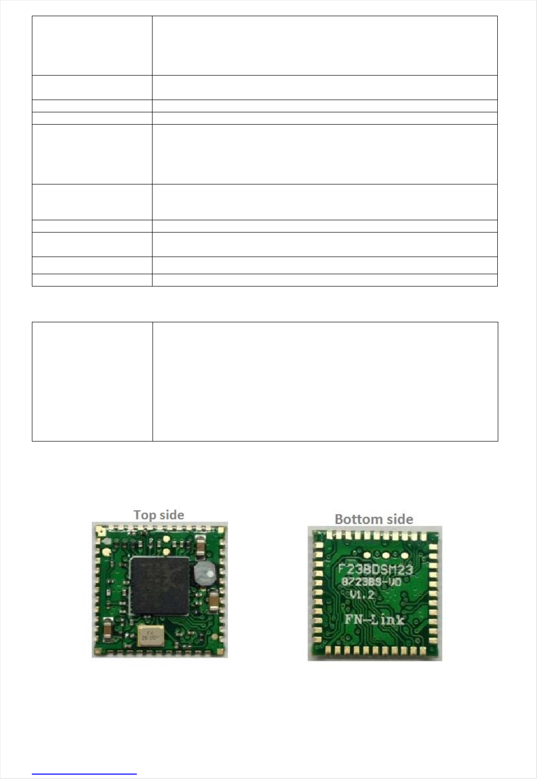
F23BDSM23-W2 is a small size and low profile of WiFi + BT Combo module with LGA (Land-Grid Array)
footprint, board size is 12mm*12mm with module thickness of 2mm. It can be easily manufactured on
SMT process and highly suitable for tablet PC, ultra book, mobile device and consumer products. It
provides SDIO interface for WiFi to connect with host processor and high speed UART interface for BT.
It also has a PCM interface for audio data transmission with direct link to external audio codec via BT
controller. The WiFi throughput can go up to 150Mbps in theory by using 1x1 802.11n b/g/n MIMO
technology and Bluetooth can support BT2.1+EDR/BT3.0 and BT4.0.
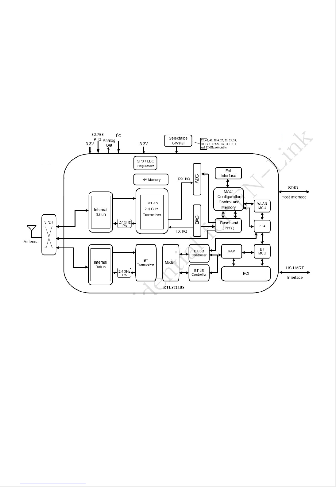
F23BDSM23-W2 uses Realtek RTL8723BS, a highly integrated WiFi/BT single chip based on
advanced COMS process. RTL8723BS integrates whole WiFi/BT function blocks into a chip, such as
SDIO/UART, MAC, BB, AFE, RFE, PA, EEPROM and LDO/SWR, except fewer passive components
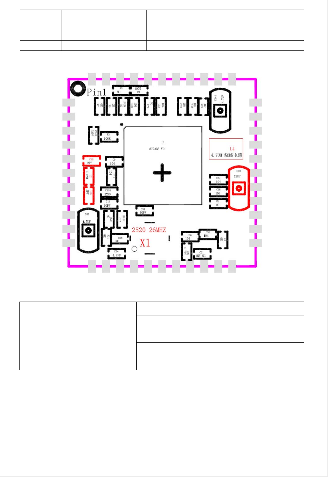
remained on PCB. The general block diagram for the module is shown in Figure 1
Figure 1
1.2 Product Features
Operate at ISM frequency bands (2.4GHz)
SDIO for WiFi and UART for Bluetooth
IEEE standards support: IEEE 802.11b, IEEE 802.11g, IEEE 802.11n, IEEE 802.11d, IEEE
802.11e, IEEE 802.11h, IEEE 802.11i
Fully Qualified for Bluetooth 2.1+EDR specification including both 2Mbps and 3Mbps modulation
mode
Fully qualified for Bluetooth 3.0
Fully qualified for Bluetooth 4.0 Dual mode
Full–speed Bluetooth operation with Piconet and Scatternet support
Enterprise level security which can apply WPA/WPA2 certification for WiFi.
WiFi 1 transmitter and 1 receiver allow data rates supporting up to 150 Mbps downstream and 150
Mbps upstream PHY rates
Note: The EUT does not support the technology MIMO .

FN-LINK TECHNOLOGY LIMITED
http://www.fn-link.com Page5/13
2. GENERAL SPECIFICATION
2.1 RF Specifications
Main Chipset Realtek RTL8723BS-VD
Operating Frequency 2.400~2.4835GHz
Standards WiFi:
IEEE 802.11b, IEEE 802.11g, IEEE 802.11n, IEEE 802.11d, IEEE
802.11e, IEEE 802.11h, IEEE 802.11i
BT:
V2.1+EDR/BT v3.0/BT v4.0
Modulation WiFi:
802.11b: CCK(11, 5.5Mbps), QPSK(2Mbps), BPSK(1Mbps),
802.11 g/n: OFDM
BT:
8DPSK, π/4 DQPSK, GFSK
PHY Data rates WiFi:
802.11b: 11,5.5,2,1 Mbps
802.11g: 54,48,36,24,18,12,9,6 Mbps
802.11n: up to 150Mbps
BT:
1 Mbps for Basic Rate
2,3 Mbps for Enhanced Data Rate
6,9,12,18,24,36,48,54 Mbps for High Speed
Transmit Output
Power WiFi:
802.11b@11Mbps <10dBm
802.11g@6Mbps <10dBm
802.11g@54Mbps <10dBm
802.11n@65Mbps <10dBm (MCS 0_HT20)
<10dBm (MCS 7_HT20)
<10dBm (MCS 0_HT40)
<10dBm (MCS 7_HT40)
BT:
<5dBm
EVM 802.11b /11Mbps : EVM≦-9dB
802.11g /54Mbps : EVM≦-25dB
802.11n /65Mbps : EVM≦-28dB
802.11b@8% PER
1Mbps -88dBm
2Mbps -87dBm
5.5Mbps -85dBm
11Mbps -82dBm
802.11g@10% PER
6Mbps -86dBm
9Mbps -85dBm
12Mbps -84dBm
18Mbps -82dBm
24Mbps -80dBm
36Mbps -77dBm
48Mbps -73dBm
54Mbps -71dBm
Receiver Sensitivity
(WiFi)
802.11n@10% PER
MCS 0 -83dBm
MCS 1 -82dBm
MCS 2 -80dBm
MCS 3 -78dBm
MCS 4 -75dBm
MCS 5 -71dBm
MCS 6 -69dBm
MCS 7 -67dBm
Receiver Sensitivity
(BT) -89dBm @ 1Mbps
-86dBm @ 2Mbps
-83dBm @ 3Mbps
FN-LINK TECHNOLOGY LIMITED
http://www.fn-link.com Page6/13
Operating Channel WiFi 2.4GHz:
11: (Ch. 1-11) – United States
13: (Ch. 1-13) – Europe
14: (Ch. 1-14) – Japan
BT 2.4GHz: Ch. 0 ~78
Media Access Control WiFi: CSMA/CA with ACK
BT: AFH, Time Division
Antenna External Antenna
Antenna Gain 3.9dBi Max
Network Architecture WiFi: Ad-hoc mode (Peer-to-Peer )
Infrastructure mode
Software AP
WiFi Direct
BT: Pico Net, Scatter Net
Security WiFi: WPA, WPA-PSK, WPA2, WPA2-PSK, WEP 64bit & 128bit, IEEE
802.11x, IEEE 802.11i
BT: Simple Paring
OS Supported Android /Linux/ Win CE /iOS /XP/WIN7
Host Interface WiFi: SDIO
BT: UART
Operating Voltage 3.3±10% Vdc I/O supply voltage
Dimension Typical L12.0*W12.0*H1.6mm
2.2 Power Consumption
Power Consumption
(Typical by using
SWR)
WiFi only:
TX Mode: (Throughput mode) 170mA (MCS7/BW40/13dBm)
RX Mode: (Throughput mode) 130mA (MCS7/BW40/-60dBm)
Associated Idle power saving with DTIM=3 2.1mA
Unassociated Idle: 0.1mA
RF disable Mode: 0.1mA
BT: Inquiry & Page Scan: 0.9 mA
ACL no traffic: 7.5mA
SCO HV3: 15.0mA
3. Mechanical Specification
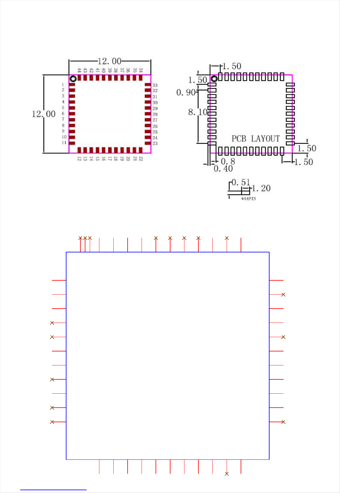
3.1 Outline Drawing (Unit: ±0.15mm)
FN-LINK TECHNOLOGY LIMITED
http://www.fn-link.com Page7/13
3.2 PCB LAYOUT Reference
3.3 Pin Definition
NC 35
SDIO_DATA_CLK
17
GND 33
SDIO_DATA_3
15
PCM_SYNC 28
SDIO_DATA_CMD
16
NC 32
SDIO_DATA_2
14
GND 31
PCM_OUT 25
TCXO_IN 30
BT_HOST_WAKE
7
WL_VDD_TXCO 29
WL_REG_ON
12
BT_WAKE
6
WL_XTAL_OUT
11
GND
20
SDIO_DATA_1
19
WL_XTAL_IN
10
NC
5
GND
3
NC
8
WL_HOST_WAKE
13
SDIO_DATA_0
18
PCM_IN 27
PCM_CLK 26
WL_BT_ANT
2
VIN_LDO_OUT
21
VIN_LDO 23
GND 36
NC 40
NC 39
BT_XTAL_OUT 38
BT_XTAL_IN 37
UART_TXD 42
TP2(NC) 46
UART_RXD 43
UART_CTS_N 44
TP1(NC) 45
GND
1
VBAT
9
VDDIO
22
UART_RTS_N 41
BT_RST_N 34
LPO 24
NC
4
TP3(NC) 47
CON1
8723BS_TFBGA

FN-LINK TECHNOLOGY LIMITED
http://www.fn-link.com Page8/13
PIN Assignment
Pin # Name Description
1 GND Ground connection
2 WL_BT_ANT RF I/O port
3 GND Ground connection
4 NC Floating (NC)
5 NC Floating (NC)
6 BT_WAKE Wake-up BT
7 BT_HOST_WAKE BT wake-up BT
8 NC Floating (NC)
9 VBAT 3.3±10% V Main power voltage source input
10 WL_XTAL_IN Floating (NC)
11 WL_XTAL_OUT Floating (NC)
12 WL_REG_ON Internal regulators power enable/disable
13 WL_HOST_WAKE WLAN wake-up HOST
14 SDIO_DATA_2 SDIO data line 2
15 SDIO_DATA_3 SDIO data line 3
16 SDIO_DATA_CMD SDIO command line
17 SDIO_DATA_CLK SDIO clock line
18 SDIO_DATA_0 SDIO data line 0
19 SDIO_DATA_1 SDIO data line 1
20 GND Ground
21 VIN_LDO_OUT Floating(NC)
22 VDDIO I/O Voltage supply input
23 VIN_LDO Floating (NC)
24 LPO External Clock input(32.768kHz), need to be reserved
25 PCM_OUT PCM Output
26 PCM_CLK PCM Clock
27 PCM_IN PCM Input
28 PCM_SYNC PCM Sync
29 WL_VDD_TXCO Floating (NC)
30 TCXO_IN Floating (NC)
31 GND Ground
32 NC Floating (NC)
33 GND Ground
34 BT_RST_N BT Reset IN
35 NC Floating (NC)
36 GND Ground
37 BT_XTAL_IN Floating (NC)
38 BT_XTAL_OUT Floating (NC)
39 NC Floating (NC)
40 NC Floating (NC)
41 UART_RTS_N UART RTS
42 UART_TXD UART Output
FN-LINK TECHNOLOGY LIMITED
http://www.fn-link.com Page9/13
43 UART_RXD UART Input
44 UART_CTS_N UART CTS
45~47 TP1~TP3 Test point1~3 Floating (NC)
Total 47PINS 12.0*12.0*1.8mm LGA Package
3.4 SMD
4. Environmental Requirements
4.1 Conditions
Temperature:0°C to +70°C
Operating
Relative Humidity: 10-90% (non-condensing)
Temperature: -40°C to +80°C (non-operating)
Storage
Relative Humidity: 5-90% (non-condensing)
MTBF (Mean Time Between Failures) Over 150,000hours
FN-LINK TECHNOLOGY LIMITED
http://www.fn-link.com Page10/13
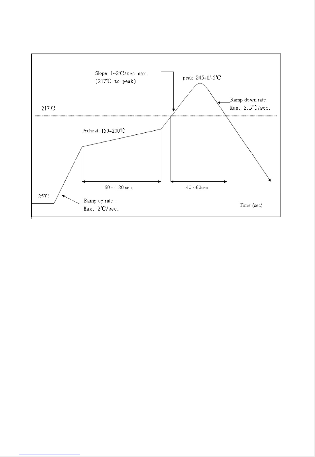
4.2 Recommended Reflow Profile
Referred to IPC/JEDEC standard.
Peak Temperature : <250°C
Number of Times : ≤2 times
4.3 Patch WIFI modules installed before the notice:
WIFI module installed note:
1. Please press 1 : 1 and then expand outward proportion to 0.7 mm, 0.12 mm thickness When open a
stencil
2. Take and use the WIFI module, please insure the electrostatic protective measures.
3. Reflow soldering temperature should be according to the customer the main size of the products,
such as the temperature set at 250 + 5 ℃ for the MID motherboard.
About the module packaging, storage and use of matters needing attention are as follows:
1. The module of the reel and storage life of vacuum packing: 1). Shelf life: 8 months, storage
environment conditions: temperature in: < 40 ℃, relative humidity: < 90% r.h.
2. The module vacuum packing once opened, time limit of the assembly:
Card: 1) check the humidity display value should be less than 30% (in blue), such as: 30% ~ 40%
(pink), or greater than 40% (red) the module have been moisture absorption.
2.) factory environmental temperature humidity control: ≦ 30% ℃, ≦ 60% r.h..
3). Once opened, the workshop the preservation of life for 168 hours.
3. Once opened, such as when not used up within 168 hours:
1). The module must be again to remove the module moisture absorption.
2). The baking temperature: 125 ℃, 8 hours.
3.) After baking, put the right amount of desiccant to seal packages.
FN-LINK TECHNOLOGY LIMITED
http://www.fn-link.com Page11/13
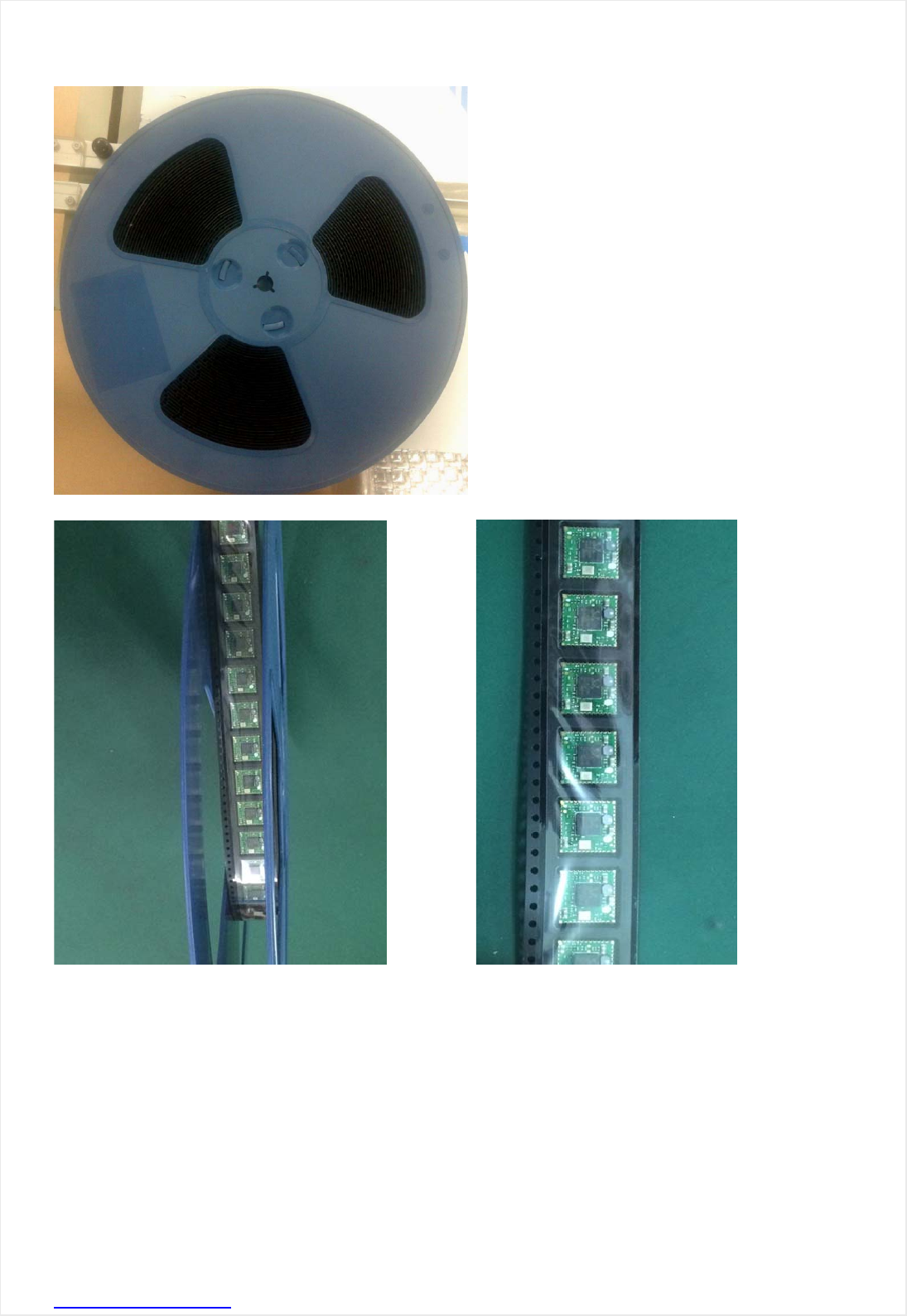
5. Package
the take-up package
Size of black tape:24mm*32.6m
Color of plastic disc:blue
A roll of 2000pcs

FN-LINK TECHNOLOGY LIMITED
http://www.fn-link.com Page12/13
FCC Statement:
This device complies with Part 15 of the FCC Rules. Operation is subject to the following
two conditions: (1) This device may not cause harmful interference. (2) This device must
accept any interference received, including interference that may cause undesired
operation.
NOTE: This equipment has been tested and found to comply with the limits for a Class B
digital device, pursuant to Part 15 of the FCC Rules. These limits are designed to provide
reasonable protection against harmful interference in a residential installation. This
equipment generates uses and can radiate radio frequency energy and, if not installed
and used in accordance with the instructions, may cause harmful interference to radio
communications. However, there is no guarantee that interference will not occur in a
particular installation. If this equipment does cause harmful interference to radio or
television reception, which can be determined by turning the equipment off and on, the
user is encouraged to try to correct the interference by one or more of the following
measures:
---Reorient or relocate the receiving antenna.
---Increase the separation between the equipment and receiver.
---Connect the equipment into an outlet on a circuit different from that to which the
receiver is connected.
---Consult the dealer or an experienced radio/TV technician for help.
WARNING: Changes or modifications not expressly approved by the party responsible for
compliance could void the user's authority to operate the equipment.
LABEL OF THE END PRODUCT:
The final end product must be labelled in a visible area with the following "Contains TX
FCC ID:
2AATL-F23BDSM23". If the size of the end product is smaller than 8x10cm, then
additional FCC part 15.19 statement is required to be available in the users manual: This
device complies with Part 15 of the FCC Rules. Operation is subject to the following two
conditions: (1) this device may not cause harmful interference, and (2) this device must
accept any interference received, including interference that may cause undesired
operation.
RF Exposure
This device has been evaluated and shown compliant with the FCC RF Exposure limits
under fixed exposure conditions (antennas are greater than 20cm from a person's body)
when installed in certain specific OEM configurations.
This modular complies with FCC RF radiation exposure limits set forth for an uncontrolled
environment. This transmitter must not be co-located or operating in conjunction with any
other antenna or transmitter. Due to missing shielding the module is strictly limited to
integration by the Grantee himself or his dedicated OEM integrator under control of the
Grantee. However, the OEM integrator is still responsible for testing their end-product for
any additional compliance requirements required with this module installed.
FN-LINK TECHNOLOGY LIMITED
http://www.fn-link.com Page13/13
IMPORTANT NOTE:
This device is intended only for OEM integrators under the following conditions:
(1) According to FCC Part 15 Subpart C Section 15.212, the radio elements of the
modular transmitter must have their own shielding. However, due to there is no shielding
for this WIFI/BT module, this module is granted as a Limited Modular Approval.
(2) This module has been designed to operate with External antenna(I-PEX connector)
having a maximum gain of 3.9dBi. The module is only certified with the installed antenna.
Any change of the antenna will void the certification.
(3) Integration is typically strictly restricted to Grantee himself or dedicated OEM
integrators under control of the Grantee.
This module is intended for OEM integrator only and the OEM integrators and instructed
to ensure that the end user has no manual instructions to remove or install the device. The
OEM integrator is still responsible for the FCC compliance requirement of the end product,
which integrates this module.
The module has no shielding and tested stand alone. This module is tested and approved
as Limited modular approval with stand alone configuration, any OEM incorporated this
radio module into any system are require additional testing and FCC Certification.
EU Regulatory Conformance
Hereby, we (FN-Link Technology Limited) declared that this device is in compliance with
the essential requirements and other relevant provisions of Directive 1999/5/EC.
NCC 警語
本模組設計之目的僅用於系統廠商組裝,不針對公眾出售。
本模組之外接發射天線(I-PEX 連接頭)最大增值增益值不可超過 3.9dBi, 任何對產品或天線的修改都會
造成產品認證的影響。
系統廠家安裝本模組後,需重新對系統作附加測試或認證評估。
經型式認證合格之低功率射頻電機,非經許可,公司、商號或使用者均不得擅自變更頻率、加大功 率或
變更原設計之特性及功能。 低功率射頻電機之使用不得影響飛航安全及干擾合法通信;經發現有干擾現
象時,應立即停用,並 改善至無干擾時方得繼續使用。前項合法通信,指依電信法規定作業之無線電通
信。低功率射頻電 機須忍受合法通信或工業、科學及醫療用電波輻射性電機設備之干擾。 本模組於取
得認證後將依規定於模組本體標示審合格籤。 系統廠商應於平台上標示「本產品內含射頻模組:
XXXyyyLPDzzzz-x (NCC ID) 」字樣。
The module Integrator will be responsible to satisfy SAR/RF exposure requirements, when the
module integrated into any (portable, mobile, fixed) host device.