Haier US Appliance Solutions BLEA003 Bluetooth 4.0 Module User Manual Product Specification

GE Appliance & Lighting Bluetooth 4.0 Module Product Specification

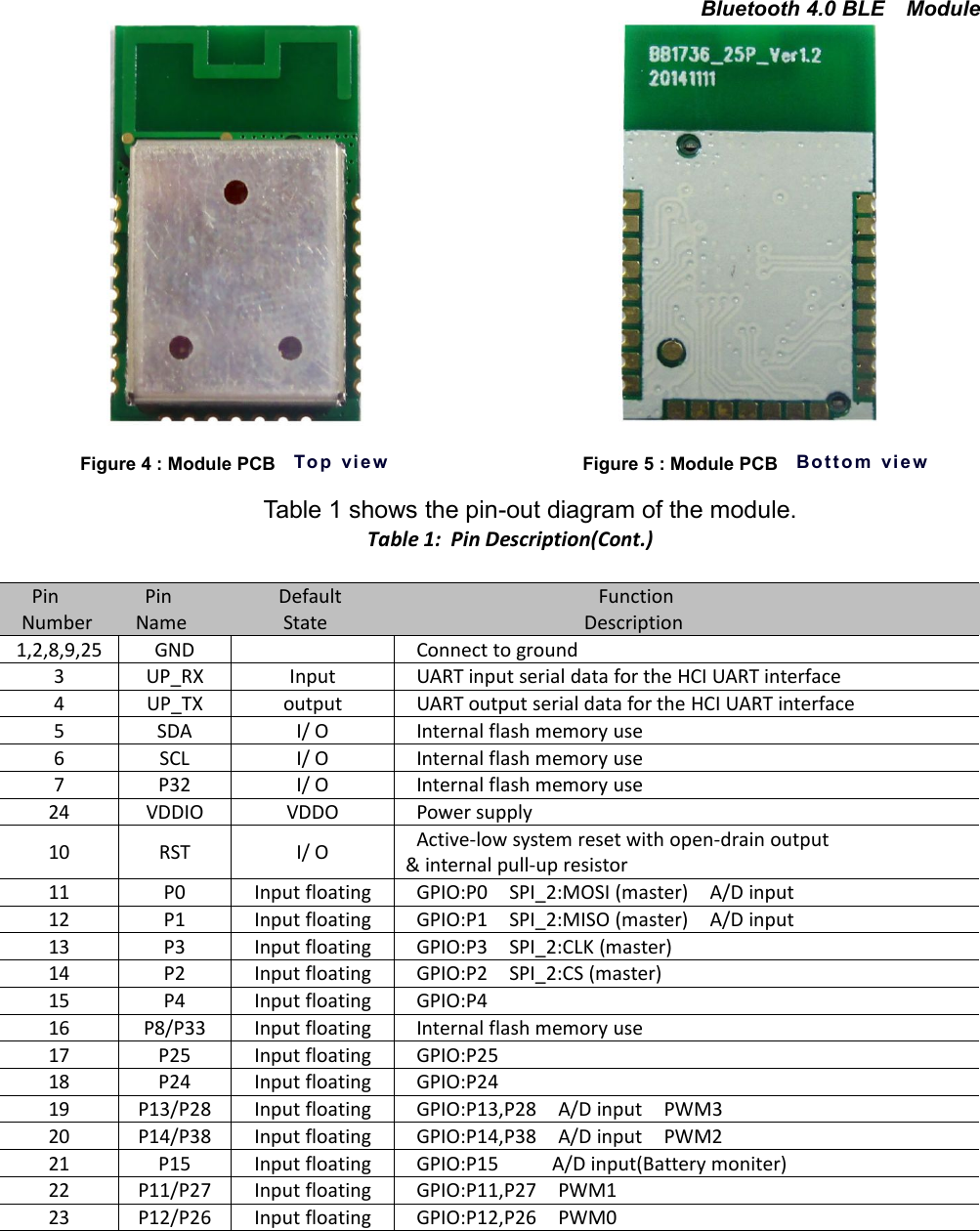
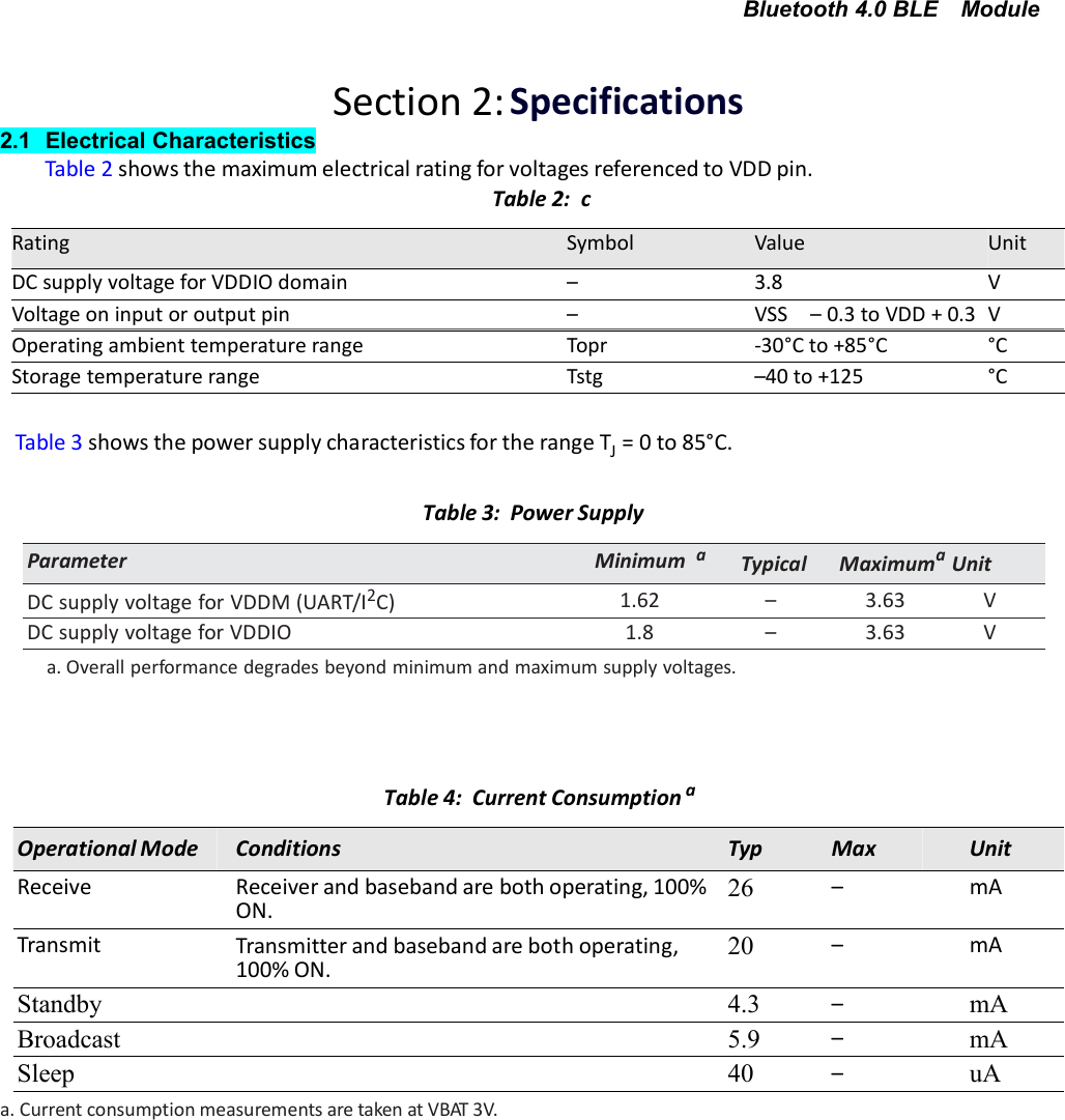
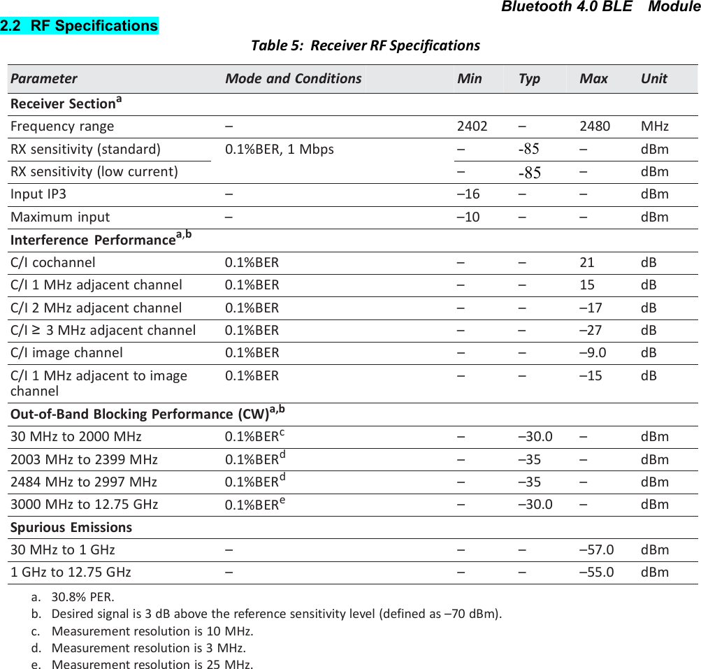
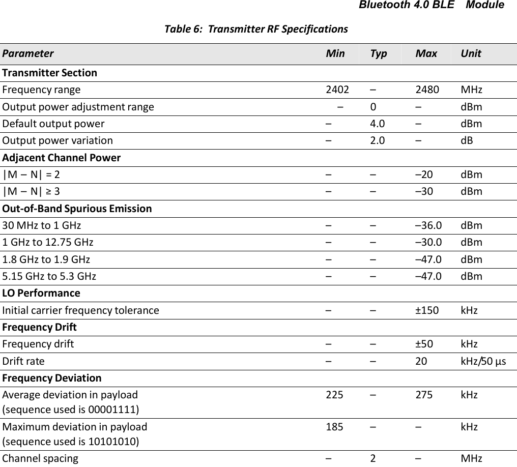
15_BB1737-25 UserMan

Bluetooth 4.0 BLE ModuleProduct SpecificationProuct: Bluetooth 4.0 BLE ModuleModule Number: BB1737-25Doc Version: V1.1Data: October 17,2015
Bluetooth 4.0 BLE ModuleSection 1:OverviewThe BB1737-25 is a Bluetooth 4.0 module based on the Broadcom BCM20737 specification basicrate-compliant stand alone baseband processor with an integrated 2.4GHz transceiver.The module includes Flash , crystal and PCB antenna.1.1 ApplicationsThe following profiles are supported in ROM:• Battery status• Blood pressure monitor• Find me• Heart rate monitor• Proximity• Thermometer• Weight scale• TimeAdditional profiles that can be supported fromRAM include:• Blood glucose monitor• Temperature alarm• Location1.2 Features• Support for RSA encryption/decryption and key exchange mechanisms (up to 4 kbit)• Support for X.509 certificate exchange• Support for NFC tag-based "tap-to-pair"• Support for Bluetooth Smart Based Audio• Bluetooth low energy (BLE)-compliant• Supports Adaptive Frequency Hopping• Excellent receiver sensitivity• 10-bit auxiliary ADC with nine analog channels• On-chip support for serial peripheral interface(SPI,UART)(master and slave modes)• Programmable output power control• Integrated ARM Cortex™-M3 based microprocessor core• Automation Profile• Support for secure OTA• On-chip power-on reset (POR)• Integrated low-dropout regulator (LDO)•On-chipsoftwarecontrolledpower management unitq• Package type:20.5*12.5*2mm FR4 PCB with 25 pads located around the perimeter.
Bluetooth 4.0 BLE Module1.3 Functional DescriptionThe primary component on the module is the Broadcom BCM20737, which is a Bluetooth 4.0 compliantbasic rate single-chip. The baseband and radio have been integrated into a single chip implemented instandard digital CMOS. The block diagram of the module is shown in Figure 1.Figure 1: Block DiagramThe BB1737-25 employs an integrated ARM CortexTM-M3 microprocessor core that runs software fromthe Link Control layer up to the Host Controller Interface (HCI).The baseband portion of the BB1737-25performs all the time-critical functions required for high-performance Bluetooth operations.The radio incorporates the complete receive and transmit paths, including PLL, VCO, LNA, PA,upconverter,downconverter, modulator, demodulator, and channel select filtering.The module has a SPI interface. The interface has a 16-byte transmit buffer and a 16-byte receivebuffer .To support more flexibility for user applications. The module acts as an SPI master device thatsupports 1.8V or 3.3V SPI slaves.
Bluetooth 4.0 BLE Module1.4 Physical DescriptionThe BB1737-25 is a 20.5*12.5*2mm FR4 PCB with 25 pads located around the perimeter Fingle2 shows the pinout diagram of the module.Fingle 2 Pin LocationFigure 3 : Module PCB Layout Mechanical Specification
Bluetooth 4.0 BLE ModuleFigure 4 : Module PCB To p v i e w Figure 5 : Module PCB B o t t o m v i e wTable 1 shows the pin-out diagram of the module.Table 1: Pin Description(Cont.)Pin Pin Default FunctionNumber Name State Description1,2,8,9,25 GND Connect to ground3 UP_RX Input UART input serial data for the HCI UART interface4 UP_TX output UART output serial data for the HCI UART interface5 SDA I/ O Internal flash memory use6 SCL I/ O Internal flash memory use7 P32 I/ O Internal flash memory use24 VDDIO VDDO Power supply10 RST I/ O Active-low system reset with open-drain output& internal pull-up resistor11 P0 Input floating GPIO:P0 SPI_2:MOSI (master) A/D input12 P1 Input floating GPIO:P1 SPI_2:MISO (master) A/D input13 P3 Input floating GPIO:P3 SPI_2:CLK (master)14 P2 Input floating GPIO:P2 SPI_2:CS (master)15 P4 Input floating GPIO:P416 P8/P33 Input floating Internal flash memory use17 P25 Input floating GPIO:P2518 P24 Input floating GPIO:P2419 P13/P28 Input floating GPIO:P13,P28 A/D input PWM320 P14/P38 Input floating GPIO:P14,P38 A/D input PWM221 P15 Input floating GPIO:P15 A/D input(Battery moniter)22 P11/P27 Input floating GPIO:P11,P27 PWM123 P12/P26 Input floating GPIO:P12,P26 PWM0
Bluetooth 4.0 BLE ModuleSection 2: Specifications2.1 Electrical CharacteristicsTable 2 shows the maximum electrical rating for voltages referenced to VDD pin.Table 2: cTable 3 shows the power supply characteristics for the range TJ= 0 to 85°C.Table 3: Power SupplyParameter Minimum aTypical MaximumaUnitDC supply voltage for VDDM (UART/I2C) 1.62 – 3.63 VDC supply voltage for VDDIO 1.8 – 3.63 Va. Overall performance degrades beyond minimum and maximum supply voltages.Table 4: Current ConsumptionaOperational ModeConditionsTypMaxUnitReceiveReceiver and baseband are both operating, 100%ON.26–mATransmitTransmitter and baseband are both operating,100% ON.20–mAStandby4.3–mABroadcast5.9–mASleep40–uAa. Current consumption measurements are taken at VBAT 3V.RatingSymbolValueUnitDC supply voltage for VDDIO domain–3.8VVoltage on input or output pin–VSS – 0.3 to VDD + 0.3VOperating ambient temperature rangeTopr-30°C to +85°C°CStorage temperature rangeTstg–40 to +125°C
Bluetooth 4.0 BLE Module2.2 RF SpecificationsTable 5: Receiver RFSpecificationsParameterMode and ConditionsMinTypMaxUnitReceiver SectionaFrequency range–2402–2480MHzRX sensitivity (standard)0.1%BER, 1 Mbps–-85–dBmRX sensitivity (low current)–-85–dBmInput IP3––16––dBmMaximum input––10––dBmInterference Performancea,bC/I cochannel0.1%BER––21dBC/I 1 MHz adjacent channel0.1%BER––15dBC/I 2 MHz adjacent channel0.1%BER–––17dBC/I ≥3 MHz adjacent channel0.1%BER–––27dBC/I image channel0.1%BER–––9.0dBC/I 1 MHz adjacent to imagechannel0.1%BER–––15dBOut-of-Band Blocking Performance (CW)a,b30 MHz to 2000 MHz0.1%BERc––30.0–dBm2003 MHz to 2399 MHz0.1%BERd––35–dBm2484 MHz to 2997 MHz0.1%BERd––35–dBm3000 MHz to 12.75 GHz0.1%BERe––30.0–dBmSpurious Emissions30 MHz to 1 GHz––––57.0dBm1 GHz to 12.75 GHz––––55.0dBma.30.8% PER.b.Desired signal is 3 dB above the reference sensitivity level (defined as –70 dBm).c.Measurement resolution is 10 MHz.d.Measurement resolution is 3 MHz.e.Measurement resolution is 25 MHz.
Bluetooth 4.0 BLE ModuleTable 6: Transmitter RF SpecificationsParameterMinTypMaxUnitTransmitter SectionFrequency range2402–2480MHzOutput power adjustment range–0–dBmDefault output power–4.0–dBmOutput power variation–2.0–dBAdjacent Channel Power|M – N| = 2–––20dBm|M – N| ≥3–––30dBmOut-of-Band Spurious Emission30 MHz to 1 GHz–––36.0dBm1 GHz to 12.75 GHz–––30.0dBm1.8 GHz to 1.9 GHz–––47.0dBm5.15 GHz to 5.3 GHz–––47.0dBmLO PerformanceInitial carrier frequency tolerance––±150kHzFrequency DriftFrequency drift––±50kHzDrift rate––20kHz/50 µsFrequency DeviationAverage deviation in payload(sequence used is 00001111)225–275kHzMaximum deviation in payload(sequence used is 10101010)185––kHzChannel spacing–2–MHz
Bluetooth 4.0 BLE ModuleONITRFOAL2.3 Timing and AC CharactristicsIn this section, use the numbers listed in the Reference column of each table to interpret the following timingdiagrams.UARTTimingTable 7: UART Timing SpecificationsReferenceCharacteristicsMinMaxUnit1Delay time, UART_CTS_N low to UART_TXD valid–24Baud outcycles2Setup time, UART_CTS_N high before midpoint of stopbit–10ns3Delay time, midpoint of stop bit to UART_RTS_N high–2Baud outcyclesFigure 6: UARTTiming
Bluetooth 4.0 BLE ModuleTONITRFOSPITimingThe SPI interface supports clock speeds up to 12 MHz with VDDIO ≥ 2.5V. The supported clock speed is 6 MHzwhen 2.5V > VDDIO ≥ 2.35V.Figure 7 and Figure 8 show the timing requirements when operating in SPI Mode 0 and 2, and SPI Mode 1and 3, respectively.Table 8: SPI Interface Timing SpecificationsReferenceCharacteristicsMinTypMax1Time from CSN asserted to first clock edge1 SCK100∞2Master setup time–½ SCK–3Master hold time½ SCK––4Slave setup time–½ SCK–5Slave hold time½ SCK––6Time from last clock edge to CSN deasserted1 SCK10 SCK1006SPI_CSNSPI_CLK1(Mode 0)SPI_CLK(Mode 2)23SPI_MOSI - FirstBitSecondBitLast bit-45SPI_MISO Not Driven FirstBitSecondBitLastbitNotDrivenFigure 7: SPITiming – Mode 0 and 2Figure 8: SPITiming – Mode 1 and 3
Bluetooth 4.0 BLE ModuleSection3: Reference DesignThe most recent schematic and design example , bill of material ,and layout file are available from theITON Technology Limit. Contact your ITON representative for details.Figure 9: Module Reference SchematicFigure 10: SPI/UART Reference InterfaceREVISION HISTORYData Revision Changes17-April-2015 1.0 Initial Version17-October-2015 1.1 Update Working Voltage
NOTE: This equipment has been tested and found to comply with the limits for a Class B digital device, pursuant to part 15 of the FCC Rules. These limits are designed to provide reasonable protection against harmful interference in a residential installation. This equipment generates, uses and can radiate radio frequency energy and, if not installed and used in accordance with the instructions, may cause harmful interference to radio communications. However, there is no guarantee that interference will not occur in a particular installation. If this equipment does cause harmful interference to radio or television reception, which can be determined by turning the equipment off and on, the user is encouraged to try to correct the interference by one or more of the following measures: —Reorient or relocate the receiving antenna. —Increase the separation between the equipment and receiver. —Connect the equipment into an outlet on a circuit different from that to which the receiver is connected. —Consult the dealer or an experienced radio/TV technician for help. Thisdevicecomplieswithpart15oftheFCCrules.Operationissubjecttothefollowingtwoconditions:(1)thisdevicemaynotcauseharmfulinterference,and(2)thisdevicemustacceptanyinterferencereceived,includinginterferencethatmaycauseundesiredoperation.Changesormodificationstothisunitnotexpresslyapprovedbythepartyresponsibleforcompliancecouldvoidtheuser'sauthoritytooperatetheequipment.
(OEM)Integratorhastoassurecomplianceoftheentireend‐productincl.theintegratedRFModule.Additionalmeasurements(15B)and/orequipmentauthorizations(e.gVerification)mayneedtobeaddresseddependingonco‐locationorsimultaenoustransmissionissuesifapplicable.Integratorisremindedtoassurethattheseinstallationinstructionswillnotbemadeavailabletotheend‐userofthefinalhostdevice.Withthelowoutputpower,thisRFModulemeetstheFCCSARexemptionandcanbethereforeintegratedintoany(portable,mobile,fixed)host Thefinalhostdevice,intowhichthisRFModuleisintegrated"hastobelabelledwithanauxilliarylablestatingtheFCCIDoftheRFModule,suchas"ContainsFCCID: ".device that powered by battery.ZKJ-BLEA003

Navigation menu