Haier US Appliance Solutions BLEA003 Bluetooth 4.0 Module User Manual Product Specification
GE Appliance & Lighting Bluetooth 4.0 Module Product Specification
15_BB1737-25 UserMan

Bluetooth 4.0 BLE Module
Product Specification
Prouct: Bluetooth 4.0 BLE Module
Module Number: BB1737-25
Doc Version: V1.1
Data: October 17,2015

Bluetooth 4.0 BLE Module
Section 1:Overview
The BB1737-25 is a Bluetooth 4.0 module based on the Broadcom BCM20737 specification basic
rate-compliant stand alone baseband processor with an integrated 2.4GHz transceiver.
The module includes Flash , crystal and PCB antenna.
1.1 Applications
The following profiles are supported in ROM:
• Battery status
• Blood pressure monitor
• Find me
• Heart rate monitor
• Proximity
• Thermometer
• Weight scale
• Time
Additional profiles that can be supported from
RAM include:
• Blood glucose monitor
• Temperature alarm
• Location
1.2 Features
• Support for RSA encryption/decryption and key exchange mechanisms (up to 4 kbit)
• Support for X.509 certificate exchange
• Support for NFC tag-based "tap-to-pair"
• Support for Bluetooth Smart Based Audio
• Bluetooth low energy (BLE)-compliant
• Supports Adaptive Frequency Hopping
• Excellent receiver sensitivity
• 10-bit auxiliary ADC with nine analog channels
• On-chip support for serial peripheral interface(SPI,UART)
(master and slave modes)
• Programmable output power control
• Integrated ARM Cortex™-M3 based microprocessor core
• Automation Profile
• Support for secure OTA
• On-chip power-on reset (POR)
• Integrated low-dropout regulator (LDO)
•
On-chip
software
controlled
power management unitq
• Package type:20.5*12.5*2mm FR4 PCB with 25 pads located around the perimeter.
Bluetooth 4.0 BLE Module
1.3 Functional Description
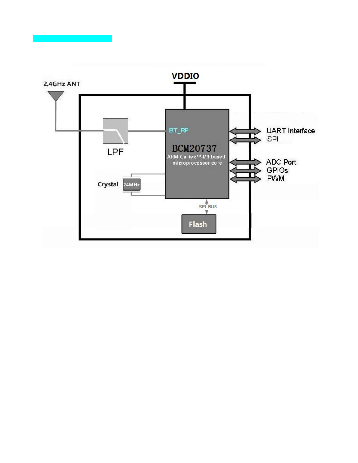
The primary component on the module is the Broadcom BCM20737, which is a Bluetooth 4.0 compliant
basic rate single-chip. The baseband and radio have been integrated into a single chip implemented in
standard digital CMOS. The block diagram of the module is shown in Figure 1.
Figure 1: Block Diagram
The BB1737-25 employs an integrated ARM CortexTM-M3 microprocessor core that runs software from
the Link Control layer up to the Host Controller Interface (HCI).The baseband portion of the BB1737-25
performs all the time-critical functions required for high-performance Bluetooth operations.
The radio incorporates the complete receive and transmit paths, including PLL, VCO, LNA, PA,
upconverter,downconverter, modulator, demodulator, and channel select filtering.
The module has a SPI interface. The interface has a 16-byte transmit buffer and a 16-byte receive
buffer .To support more flexibility for user applications. The module acts as an SPI master device that
supports 1.8V or 3.3V SPI slaves.
Bluetooth 4.0 BLE Module
1.4 Physical Description
The BB1737-25 is a 20.5*12.5*2mm FR4 PCB with 25 pads located around the perimeter Fingle
2 shows the pinout diagram of the module.
Fingle 2 Pin Location
Figure 3 : Module PCB Layout Mechanical Specification
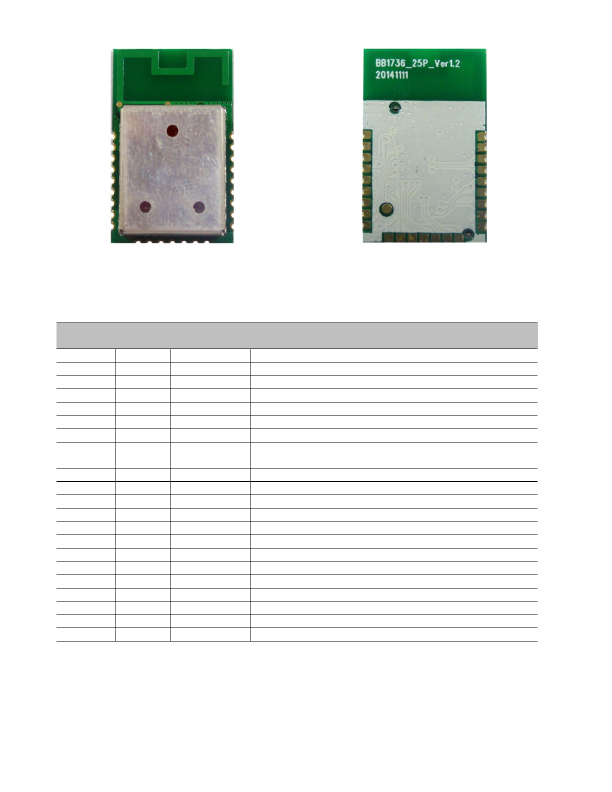
Bluetooth 4.0 BLE Module
Figure 4 : Module PCB To p v i e w Figure 5 : Module PCB B o t t o m v i e w
Table 1 shows the pin-out diagram of the module.
Table 1: Pin Description
(Cont.)
Pin Pin Default Function
Number Name State Description
1,2,8,9,25 GND Connect to ground
3 UP_RX Input UART input serial data for the HCI UART interface
4 UP_TX output UART output serial data for the HCI UART interface
5 SDA I/ O Internal flash memory use
6 SCL I/ O Internal flash memory use
7 P32 I/ O Internal flash memory use
24 VDDIO VDDO Power supply
10 RST I/ O Active-low system reset with open-drain output
& internal pull-up resistor
11 P0 Input floating GPIO:P0 SPI_2:MOSI (master) A/D input
12 P1 Input floating GPIO:P1 SPI_2:MISO (master) A/D input
13 P3 Input floating GPIO:P3 SPI_2:CLK (master)
14 P2 Input floating GPIO:P2 SPI_2:CS (master)
15 P4 Input floating GPIO:P4
16 P8/P33 Input floating Internal flash memory use
17 P25 Input floating GPIO:P25
18 P24 Input floating GPIO:P24
19 P13/P28 Input floating GPIO:P13,P28 A/D input PWM3
20 P14/P38 Input floating GPIO:P14,P38 A/D input PWM2
21 P15 Input floating GPIO:P15 A/D input(Battery moniter)
22 P11/P27 Input floating GPIO:P11,P27 PWM1
23 P12/P26 Input floating GPIO:P12,P26 PWM0

Bluetooth 4.0 BLE Module
Section 2: Specifications
2.1 Electrical Characteristics
Table 2 shows the maximum electrical rating for voltages referenced to VDD pin.
Table 2: c
Table 3 shows the power supply characteristics for the range TJ= 0 to 85°C.
Table 3: Power Supply
Parameter Minimum aTypical MaximumaUnit
DC supply voltage for VDDM (UART/I2C) 1.62 – 3.63 V
DC supply voltage for VDDIO 1.8 – 3.63 V
a. Overall performance degrades beyond minimum and maximum supply voltages.
Table 4: Current Consumption
a
Operational Mode
Conditions
Typ
Max
Unit
Receive
Receiver and baseband are both operating, 100%
ON.
26
–
mA
Transmit
Transmitter and baseband are both operating,
100% ON.
20
–
mA
Standby
4.3
–
mA
Broadcast
5.9
–
mA
Sleep
40
–
uA
a. Current consumption measurements are taken at VBAT 3V.
Rating
Symbol
Value
Unit
DC supply voltage for VDDIO domain
–
3.8
V
Voltage on input or output pin
–
VSS – 0.3 to VDD + 0.3
V
Operating ambient temperature range
Topr
-30°C to +85°C
°C
Storage temperature range
Tstg
–40 to +125
°C

Bluetooth 4.0 BLE Module
2.2 RF Specifications
Table 5: Receiver RF
Specifications
Parameter
Mode and Conditions
Min
Typ
Max
Unit
Receiver Sectiona
Frequency range
–
2402
–
2480
MHz
RX sensitivity (standard)
0.1%BER, 1 Mbps
–
-85
–
dBm
RX sensitivity (low current)
–
-85
–
dBm
Input IP3
–
–16
–
–
dBm
Maximum input
–
–10
–
–
dBm
Interference Performancea,b
C/I cochannel
0.1%BER
–
–
21
dB
C/I 1 MHz adjacent channel
0.1%BER
–
–
15
dB
C/I 2 MHz adjacent channel
0.1%BER
–
–
–17
dB
C/I ≥3 MHz adjacent channel
0.1%BER
–
–
–27
dB
C/I image channel
0.1%BER
–
–
–9.0
dB
C/I 1 MHz adjacent to image
channel
0.1%BER
–
–
–15
dB
Out-of-Band Blocking Performance (CW)a,b
30 MHz to 2000 MHz
0.1%BERc
–
–30.0
–
dBm
2003 MHz to 2399 MHz
0.1%BERd
–
–35
–
dBm
2484 MHz to 2997 MHz
0.1%BERd
–
–35
–
dBm
3000 MHz to 12.75 GHz
0.1%BERe
–
–30.0
–
dBm
Spurious Emissions
30 MHz to 1 GHz
–
–
–
–57.0
dBm
1 GHz to 12.75 GHz
–
–
–
–55.0
dBm
a.
30.8% PER.
b.
Desired signal is 3 dB above the reference sensitivity level (defined as –70 dBm).
c.
Measurement resolution is 10 MHz.
d.
Measurement resolution is 3 MHz.
e.
Measurement resolution is 25 MHz.

Bluetooth 4.0 BLE Module
Table 6: Transmitter RF Specifications
Parameter
Min
Typ
Max
Unit
Transmitter Section
Frequency range
2402
–
2480
MHz
Output power adjustment range
–
0
–
dBm
Default output power
–
4.0
–
dBm
Output power variation
–
2.0
–
dB
Adjacent Channel Power
|M – N| = 2
–
–
–20
dBm
|M – N| ≥3
–
–
–30
dBm
Out-of-Band Spurious Emission
30 MHz to 1 GHz
–
–
–36.0
dBm
1 GHz to 12.75 GHz
–
–
–30.0
dBm
1.8 GHz to 1.9 GHz
–
–
–47.0
dBm
5.15 GHz to 5.3 GHz
–
–
–47.0
dBm
LO Performance
Initial carrier frequency tolerance
–
–
±150
kHz
Frequency Drift
Frequency drift
–
–
±50
kHz
Drift rate
–
–
20
kHz/50 µs
Frequency Deviation
Average deviation in payload
(sequence used is 00001111)
225
–
275
kHz
Maximum deviation in payload
(sequence used is 10101010)
185
–
–
kHz
Channel spacing
–
2
–
MHz
Bluetooth 4.0 BLE Module
O
N
I
T
R
F
OA
L
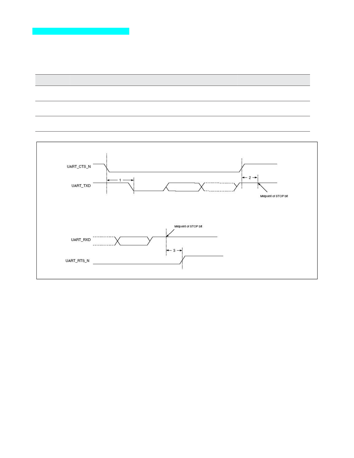
2.3 Timing and AC Charactristics
In this section, use the numbers listed in the Reference column of each table to interpret the following timing
diagrams.
UART
T
iming
Table 7: UART Timing Specifications
Reference
Characteristics
Min
Max
Unit
1
Delay time, UART_CTS_N low to UART_TXD valid
–
24
Baud out
cycles
2
Setup time, UART_CTS_N high before midpoint of stop
bit
–
10
ns
3
Delay time, midpoint of stop bit to UART_RTS_N high
–
2
Baud out
cycles
Figure 6: UART
Timing
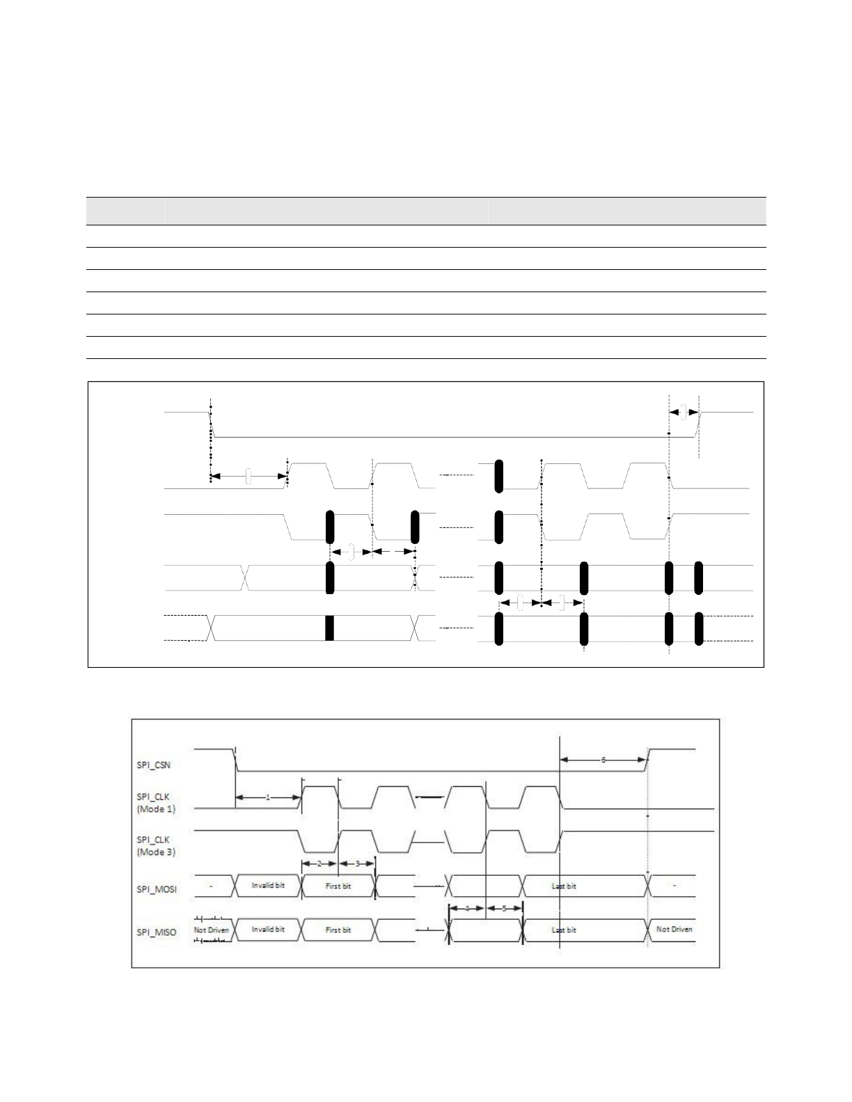
Bluetooth 4.0 BLE Module
T
O
N
I
T
R
F
O
SPI
T
iming
The SPI interface supports clock speeds up to 12 MHz with VDDIO ≥ 2.5V. The supported clock speed is 6 MHz
when 2.5V > VDDIO ≥ 2.35V.
Figure 7 and Figure 8 show the timing requirements when operating in SPI Mode 0 and 2, and SPI Mode 1
and 3, respectively.
Table 8: SPI Interface Timing Specifications
Reference
Characteristics
Min
Typ
Max
1
T
ime from CSN asserted to first clock edge
1 SCK
100
∞
2
Master setup time
–
½ SCK
–
3
Master hold time
½ SCK
–
–
4
Slave setup time
–
½ SCK
–
5
Slave hold time
½ SCK
–
–
6
T
ime from last clock edge to CSN deasserted
1 SCK
10 SCK
100
6
SPI_CSN
SPI_CLK
1
(Mode 0)
SPI_CLK
(Mode 2)
2
3
SPI_MOSI - First
Bit
Second
Bit
Last bit
-
4
5
SPI_MISO Not Driven First
Bit
Second
Bit
Last
bit
Not
Driven
Figure 7: SPI
T
iming – Mode 0 and 2
Figure 8: SPI
T
iming – Mode 1 and 3
Bluetooth 4.0 BLE Module
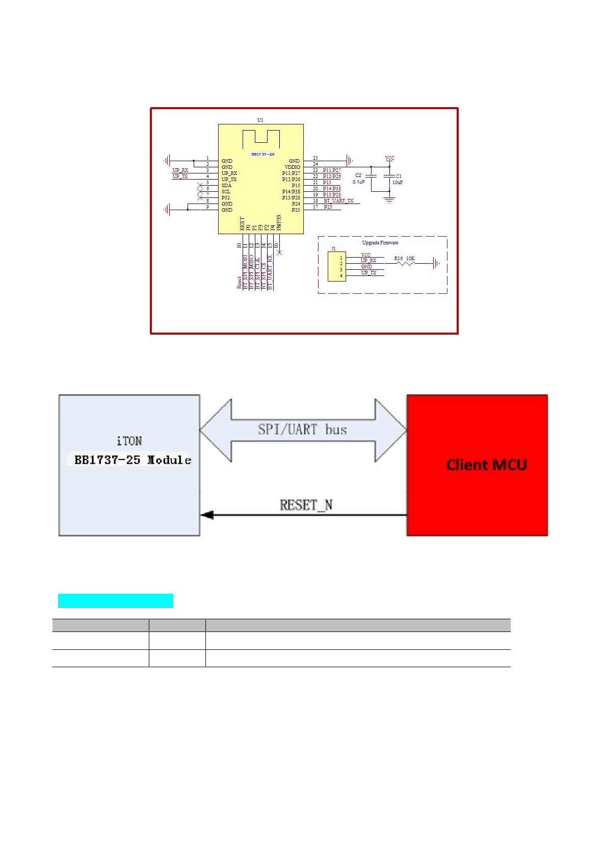
Section3: Reference Design
The most recent schematic and design example , bill of material ,and layout file are available from the
ITON Technology Limit. Contact your ITON representative for details.
Figure 9: Module Reference Schematic
Figure 10: SPI/UART Reference Interface
REVISION HISTORY
Data Revision Changes
17-April-2015 1.0 Initial Version
17-October-2015 1.1 Update Working Voltage

NOTE: This equipment has been tested and found to comply with the limits for a Class B digital
device, pursuant to part 15 of the FCC Rules. These limits are designed to provide reasonable protection
against harmful interference in a residential installation. This equipment generates, uses and can radiate
radio frequency energy and, if not installed and used in accordance with the instructions, may cause
harmful interference to radio communications. However, there is no guarantee that interference will not
occur in a particular installation. If this equipment does cause harmful interference to radio or television
reception, which can be determined by turning the equipment off and on, the user is encouraged to try to
correct the interference by one or more of the following measures:
—Reorient or relocate the receiving antenna.
—Increase the separation between the equipment and receiver.
—Connect the equipment into an outlet on a circuit different from that to which the receiver is
connected.
—Consult the dealer or an experienced radio/TV technician for help.
Thisdevicecomplieswithpart15oftheFCCrules.Operationissubjecttothefollowingtwo
conditions:
(1)thisdevicemaynotcauseharmfulinterference,and
(2)thisdevicemustacceptanyinterferencereceived,includinginterferencethatmaycause
undesiredoperation.
Changesormodificationstothisunitnotexpresslyapprovedbythepartyresponsiblefor
compliancecouldvoidtheuser'sauthoritytooperatetheequipment.
(OEM)Integratorhastoassurecomplianceoftheentireend‐product
incl.theintegratedRFModule.Additionalmeasurements(15B)and/orequipmentauthorizations
(e.gVerification)mayneedtobeaddresseddependingonco‐locationorsimultaenous
transmissionissuesifapplicable.
Integratorisremindedtoassurethattheseinstallationinstructions
willnotbemadeavailabletotheend‐userofthefinalhostdevice.
Withthelowoutputpower,thisRFModulemeetstheFCCSARexemption
andcanbethereforeintegratedintoany(portable,mobile,fixed)host
Thefinalhostdevice,intowhichthisRFModuleisintegrated"hastobelabelled
withanauxilliarylablestatingtheFCCIDoftheRFModule,suchas
"ContainsFCCID: ".
device that powered by battery.
ZKJ-BLEA003