Hangzhou Gubei Electronics Technology BL3335-P WiFi Module User Manual
Hangzhou Gubei Electronics Technology Co.,Ltd WiFi Module
User Manual

World’s leading smart home solution provider
Features
Support IEEE802.11 b/g/n standards
Support WEP, WPA and WPA2 encryption
Support UART/PWM/ADC/GPIO/I2C
interfaces
Support STA/AP/AP+STA modes
Support SmartConfig
Support TLS/SSL protocols
Support PCB antenna
3.3V power supply
Wi-Fi related features
Support 802.11 b/g/n with 20M
and 40M bandwidth
Support station and soft AP
Support SmartConfig and AP
configuration
Integrated balun/PA/LNA
TCP/IP stack optimized for IoT
application
PCB antenna
Peripheral
2x UART
1x I2C
1x SPI
4x PWM
Up to 14GPIOs
Working temperature: -10℃to +85℃
Stamp style SMD for surface mounting
production
Applications
Smart transportation
Smart home / appliances
Instruments
Health care
Industrial automation
Intelligent security
Smart energy
Models
Model Antenna type Note
BL3335-P PCB antenna Default
Version:1.0 Release date:Jan 12, 2018
BL3335-P Embedded
Product
Manual

-2-
Content
1. Overview.............................................................................................................................- 3 -
2. Basic Specifications.............................................................................................................- 3 -
2.1. Power Consumption.................................................................................................... - 3 -
2.2. Working Environment..................................................................................................- 4 -
3. Radio Specifications............................................................................................................- 4 -
3.1. Basic Radio Specification............................................................................................. - 4 -
3.2. Radio Performance...................................................................................................... - 5 -
3.2.1. IEEE 802.11b......................................................................................................... - 5 -
3.2.2. IEEE 802.11g......................................................................................................... - 5 -
3.2.3 IEEE802.11n........................................................................................................... - 6 -
4. BL3335-P Hardware Information........................................................................................- 8 -
4.1. Footprint Sequence..................................................................................................... - 8 -
4.2. Footprint Definitions................................................................................................... - 9 -
4.3. PCB Antenna.............................................................................................................. - 10 -
4.4. Mechanical Dimensions.............................................................................................- 12 -
4.5. Recommended Pad Size............................................................................................ - 13 -
5. Reference Design..............................................................................................................- 14 -
5.1. UART Interface Design...............................................................................................- 14 -
5.2. Power Supply Requirement.......................................................................................- 15 -
Revision History.................................................................................................................... - 16 -
Copyrights.............................................................................................................................- 16 -
Contact Us.............................................................................................................................- 16 -
-3-
1. Overview
BL3335-P is a cost-effective embedded Wi-Fi module designed by BroadLink, which supports
802.11 b/g/n standards and UART communication with other devices. The module integrates
radio transceiver, MAC, baseband, all Wi-Fi protocols, configurations and network stack. It can be
widely used in applications like smart home devices, remote monitoring devices and medical care
instruments.
The module integrates an ARM Cortex-M4 processor speed up to 160MHz with 352KB SRAM
and 1MB flash.
2. Basic Specifications
2.1. Power Consumption
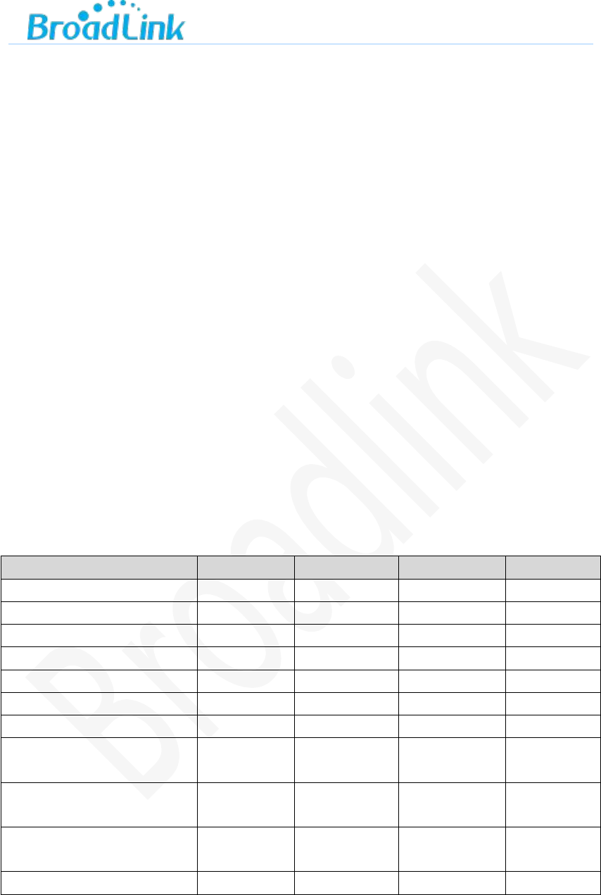
Please refer to Table 1 for power consumption data.
Table 1 BL3335-P Power Consumption Data
Specifications Min. Typ. Max. Units
VDD13.3 4 V
VIL(input low voltage) 0 0.3VDD V
VIH(input high voltage) 0.7VDD VDD V
VOL(output low voltage) 0 V
VOH(output high voltage) VDD V
Io 10 mA
Standby (SP mini) 80 85 mA
pulse current @TX
11b @17dBm 11Mbps
305 mA
pulse current @TX
11g @15dBm 54Mbps
250 mA
pulse current @TX
11n @14dBm 65Mbps
225 mA
Networking 305 mA
Note: Make sure VDD is not lower than 3.3V
-4-
2.2. Working Environment
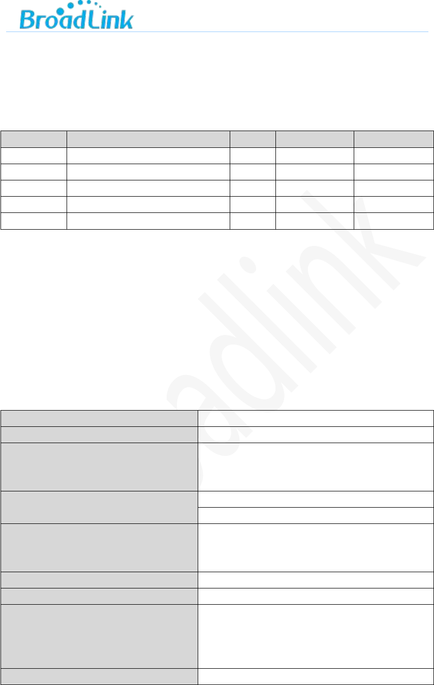
Please refer to Table 2 for working environment data.
Table 2 BL3335-P Working Environment Data
Symbol Description Min. Max. Units
Ts Storage temperature -40 125 ℃
TAAmbient operating temperature -10 85 ℃
Vdd Supply voltage 3.3 4 V
Vio Voltage on IO pin 0 VDD V
ESD HBM 1000 2000 V
3. Radio Specifications
3.1. Basic Radio Specification
Please refer to Table 3 for radio specification.
Table 3 BL3335-P Radio Specification
Radio range 2.412 GHz - 2.462 GHz
Wireless standards IEEE 802.11 b/g/n
Radio output
802.11b :18dBm ± 1dBm
802.11g :15dBm ± 1dBm
802.11n :13dBm ± 2dBm
Antenna type Internal: PCB antenna
External: Not supported
Receiving sensitivity
802.11b<-83dBm@11Mbps
802.11g<-72dBm@54Mbps
802.11n<-71dBm@MCS7
Stack IPv4, TCP/UDP/FTP/HTTP/HTTPS/TLS/mDNS
Data rate (max) 11M@802.11b, 54M@802.11g, MCS7@802.11n
Security
Encryption standard:
Open/WEP-Open/WPA/WPA2
Encryption algorithm:
WEP64/WEP128/TKIP/AES
Network types STA/AP/STA+AP/WIFI Direct
-5-
3.2. Radio Performance
3.2.1. IEEE 802.11b
Table 4 Basic specifications under IEEE802.11b
ITEM Specification
Modulation Type DSSS / CCK
Frequency range 2412MHz~2462MHz
Channel CH1 to CH11
Data rate 1, 2, 5.5, 11Mbps
Table 5 Transmitting performance under IEEE802.11b
TX Characteristics Min. Typical Max. Unit
Power@11Mbps 17 dBm
Frequency Error -10 +10 ppm
EVM@11Mbps -20 dB
Transmit spectrum mask
Pass
Table 6 Receiving performance under IEEE802.11b
RX Characteristics Min
.
Typical Max. Unit
Minimum Input Level Sensitivity
11Mbps (FER≦8%) -83 dBm
Maximum Input Level (FER≦8%) -3 dBm
3.2.2. IEEE 802.11g
Table 7 Basic specifications under IEEE802.11g
ITEM Specification
Modulation Type OFDM
Frequency range 2412MHz~2462MHz
-6-
Channel CH1 to CH11
Data rate 6, 9, 12, 18, 24, 36, 48, 54Mbps
Table 8 Transmitting performance under IEEE802.11g
TX Characteristics Min. Typical Max. Unit
Power@54Mbps 14 dBm
Frequency Error -10 +10 ppm
EVM@54Mbps -30 -29 dB
Transmit spectrum mask
Pass
Table 9 Receiving performance under IEEE802.11g
RX Characteristics Min. Typical Max. Unit
Minimum Input Level Sensitivity
54Mbps -71 dBm
Maximum Input Level
(FER≦10%)
-8 dBm
3.2.3 IEEE802.11n
IEEE802.11n 20MHz bandwidth mode
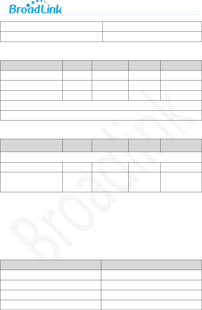
Table 10 Basic specifications under IEEE802.11n with 20MHz
ITEM Specification
Modulation Type OFDM
Frequency range 2412MHz~2462MHz
Channel CH1 to CH11
Data rate MCS0/1/2/3/4/5/6/7
-7-
Table 11 Transmitting performance under IEEE802.11n with 20MHz
TX Characteristics Min. Typical Max. Unit
Power@HT20, MCS7 14 dBm
Frequency Error -10 +10 ppm
EVM@HT20, MCS7 -29 dB
Transmit spectrum mask
Pass
Table 12 Receiving performance under IEEE802.11n with 20MHz
RX Characteristics Min. Typical Max. Unit
Minimum Input Level Sensitivity
MCS7 -69 dBm
Maximum Input Level
(FER≦10%)
-8 dBm
IEEE802.11n 40MHz bandwidth mode
Table 13 Basic specifications under IEEE802.11n with 40MHz
ITEM Specification
Modulation Type OFDM
Frequency range 2422MHz~2452MHz
Channel CH3 to CH9
Data rate MCS0/1/2/3/4/5/6/7
Table 14 Transmitting performance under IEEE802.11n with 40MHz
TX Characteristics Min. Typical Max. Unit
Power@HT40, MCS7 14 dBm
Frequency Error -10 +10 ppm
EVM@HT40, MCS7 -33 dB
Transmit spectrum mask
Pass
-8-
Table 15 Receiving performance under IEEE802.11n with 40MHz
RX Characteristics Min. Typical Max. Unit
Minimum Input Level Sensitivity
MCS7 -68 dBm
Maximum Input Level
(FER≦10%)
-8 dBm
4. BL3335-P Hardware Information
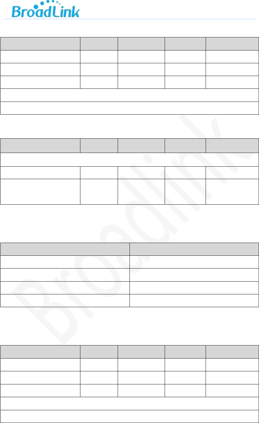
4.1. Footprint Sequence
Please refer to Fig 1 for the footprint sequence of BL3335-P.
Fig 1 BL3335-P Footprint sequence

-9-
4.2. Footprint Definitions
Please refer to Table 16 for the footprint definitions of BL3335-P.
Table 16 BL3335-P footprint definitions
pin
Function
1
Function
2
Function
3
Function
4
Function
5
Default
state
1 GPIO2 TX2 UP
2 GPIO1 RX2 I2C_SDA UP
3 GPIO3 I2C_SCK UP
4 GPIO12 SPI_MOSI DOWN
5 GPIO13 SPI_MISO PWM1 DOWN
6 GPIO25 PWM3 DOWN
7 GPIO0 PWM2 DOWN
8 VDD
9 GND
10 PDN
11 GPADC GPIO6 DOWN
12 GPIO7 DOWN
13 GPIO8 PWM0 DOWN
14 GPIO5 SPI_CS DOWN
15 GPIO4 SPI_CLK DOWN
16 RX0 GPIO_26 DOWN

- 10 -
17 TX0 GPIO_27 DOWN
18 GND
Note:
1. In default, UART2 (pin1 and pin2) are used for bypass communication and UART0
(pin16 and pin17) are used for output of debugging information and burning firmware. Please
refer to the description in DC Characteristics for UART output current level.
2. PDN is hardware reset for the module and will be effective with VIL. Configuration
information will be remained after module reset. The module has pull-up process for PDN
designed internally.
3. In default, PIN13 (GPIO8) is the PIN for external LED indicator to show the module
configuration status and output VIH after configuration is successful.
4. In default, PIN14 (GPIO5) is the module software reset PIN and will be effective with
VIH. The previous configuration information will be cleared after the module is reset (reset to
factory settings).
5. The module supports max 4 channels of external interruption simultaneously except
GPIO25 and UART0.
6. The ADC is 10bit with input voltage 0-2V
7. The power supply VDD should not be lower than 3.3V.
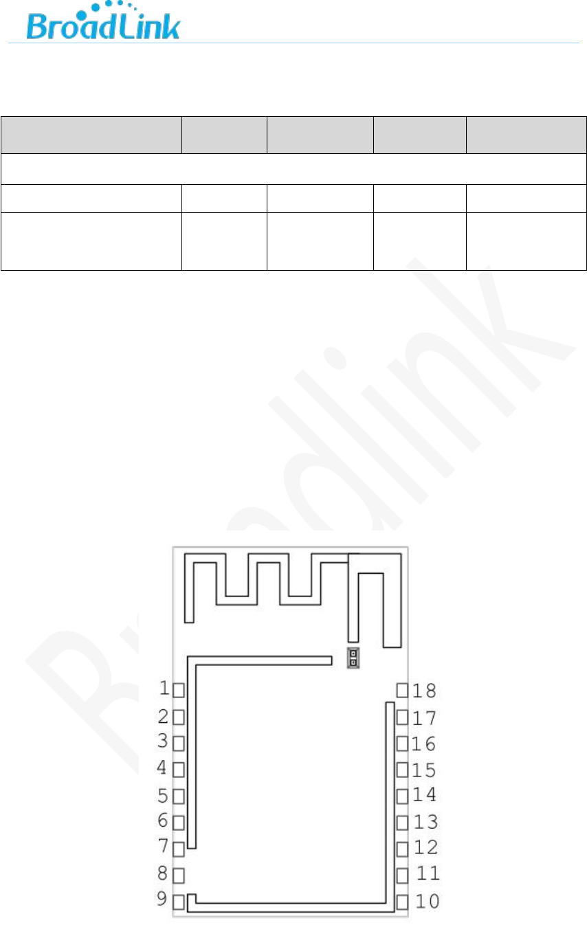
4.3. PCB Antenna
Please refer to Fig 2 for PCB antenna. Please avoid to place any electrical components,
wiring or grounding under PCB antenna area on main board and it’s better to leave this area
blank on PCB.
- 11 -
Fig 2 BL3335-P Antenna
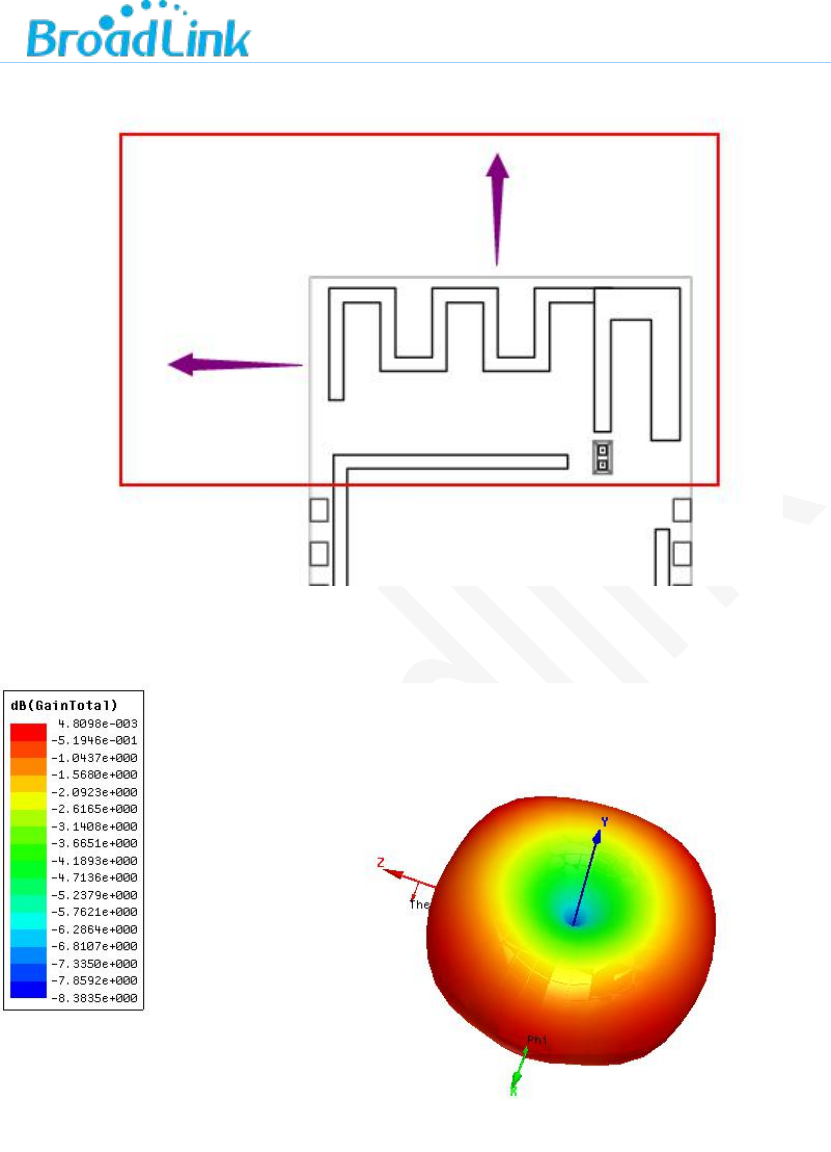
The gain of PCB antenna on this module is about 0dB, as shown in Fig Fig 3.
Fig 3 Simulated radiation pattern of antenna gain
The following precautions should be considered during designing with PCB antenna:
1. Do not place any electrical components or grounding in antenna area on main board and
it’s better to leave this area blank on PCB.
2. It is recommended to not place any electrical components within 30mm range of module
- 12 -
antenna and not design any circuit or bond copper on main board under this area.
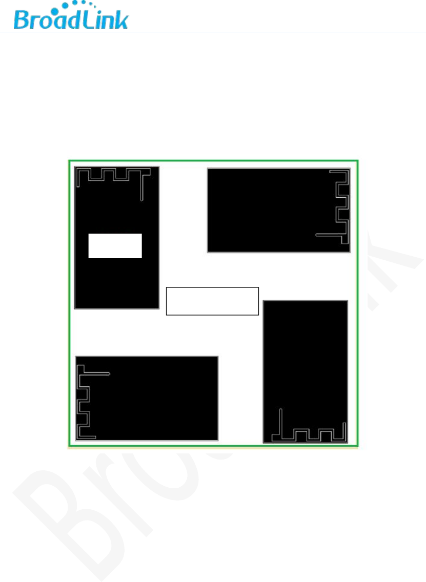
3. Do not use the module inside any metal case or containers with metal painting.
4. Keep the antenna of wifi module next to the edge of main board during design of PCB to
ensure better performance of antenna, as illustrated below.
Fig 4 BL3335-P Recommended PCB layout
4.4. Mechanical Dimensions
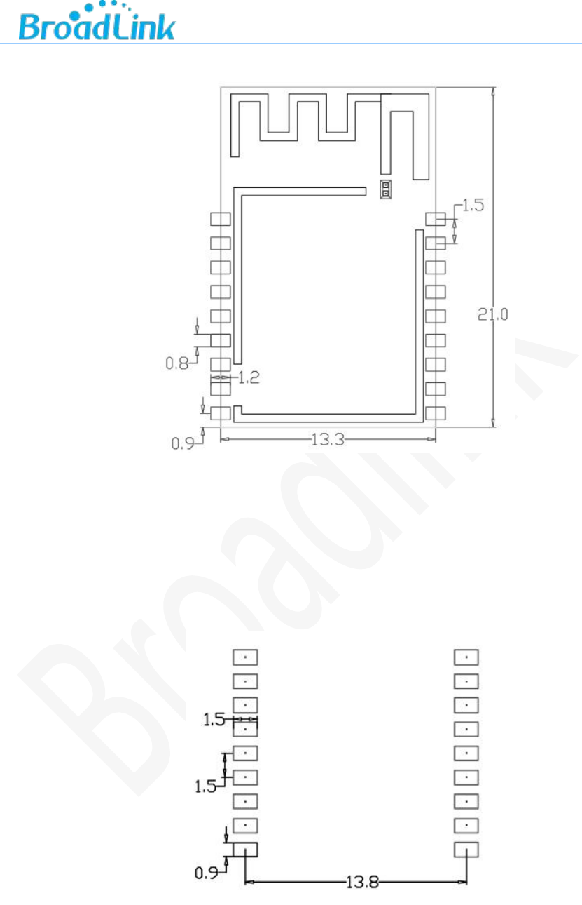
Please refer to Fig Fig 5 for the dimensions of BL3335-P module.
Module
Device PCB
- 13 -
Fig 5 BL3335-P Dimensions
a.Note: Dimensions (13.3±0.2) mm * (21±0.2) mm * (2.6±0.2)mm (with shielding case)
4.5. Recommended Pad Size
Please refer to Fig Fig 6 for the recommended pad size of BL3335-P module.
Fig 6 BL3335-P Recommended pad size
Unit: mm
- 14 -
5. Reference Design
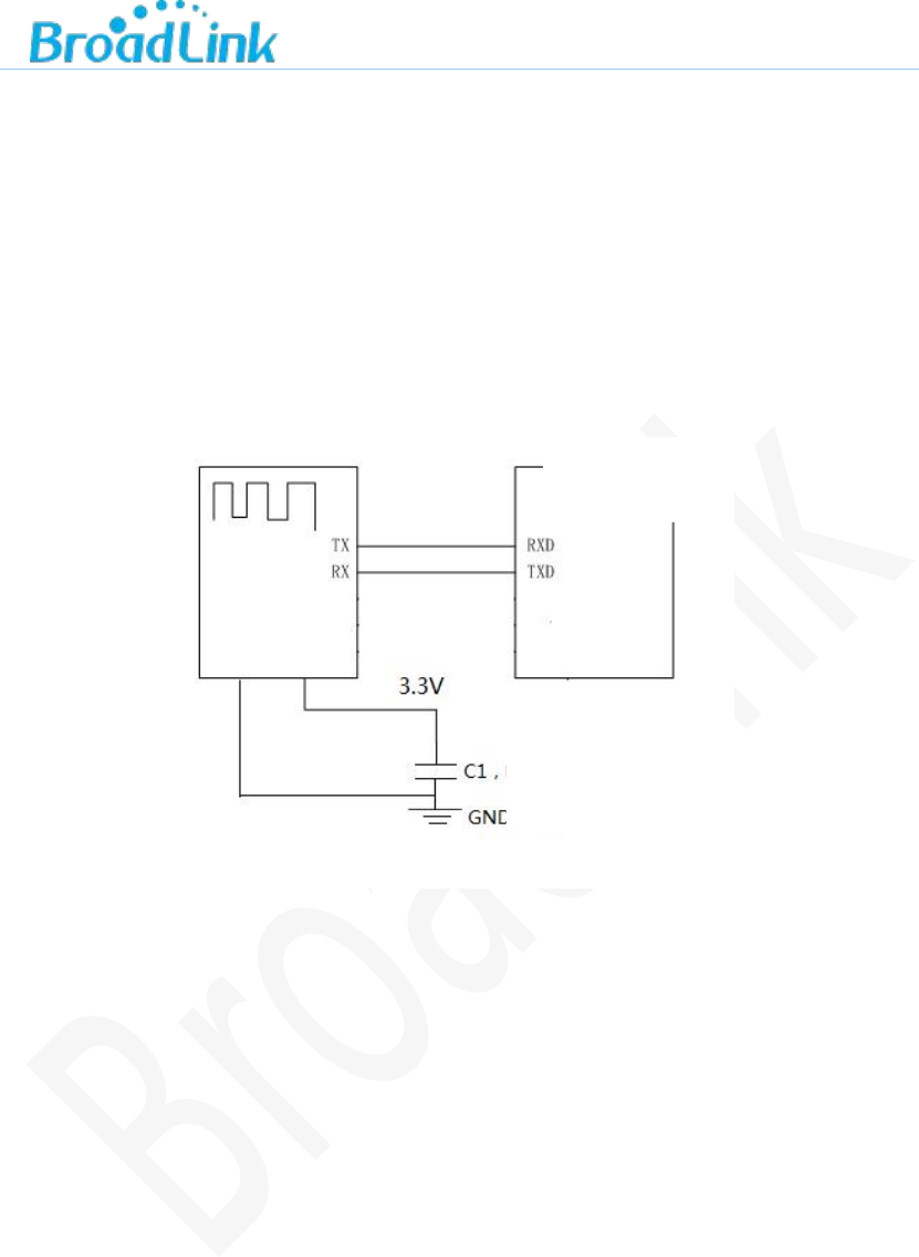
5.1. UART Interface Design
For devices with 3.3V power supply, you can directly connect the device UART port with
module UART port according to the illustration in Fig Fig 7.
Fig 7 Circuit diagram (3.3V)
If your device is powered by 5V, you can refer to the circuit shown in Fig Fig 8 or design your
own circuit for power conversion. The value of resistor can be adjusted according to actual circuit
design.
Wi-Fi
module
External
MCU
Capacitor
Grounding
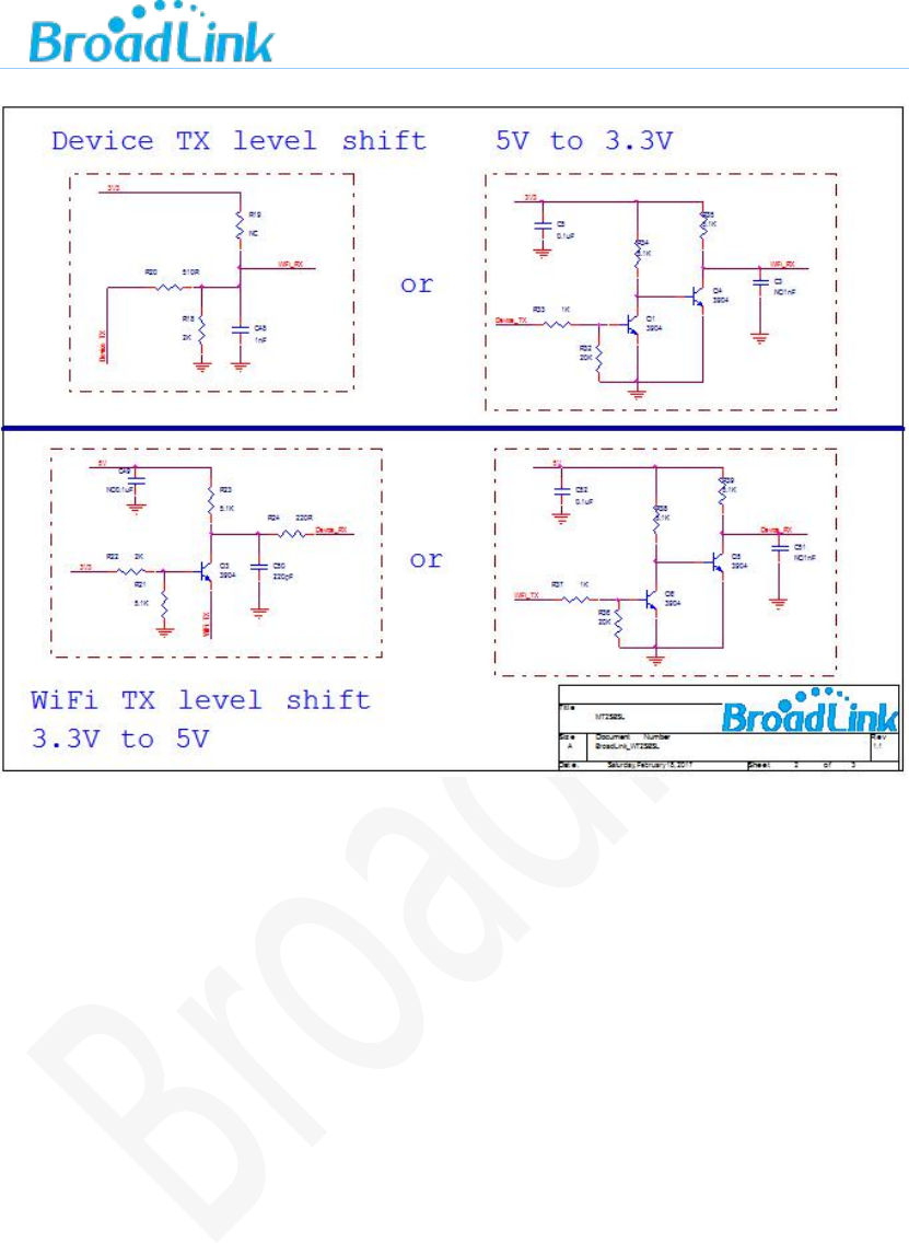
- 15 -
Fig 8 Circuit diagram (5V)
5.2. Power Supply Requirement
If an LDO is used to supply the module with 3.3V power, C1 capacitor can be considered to
be used with 10u-22u; If a DCDC is used to supply 3.3V power, C1 capacitor can be considered to
be used with 22uF.
It is recommended to supply the module with power higher than 400mA to ensure enough
power supply to the module and avoid power down during data transmission.
- 16 -
Revision History
Date
Version
Updated Content
Jan 12, 2018
1.0
Preliminary version
Copyrights
It is prohibited to use or copy all or any part of contents in this manual without
prior permission, especially applicable for trademarks, models, part numbers and
figures.
Contact Us
Ms Zhou
Hangzhou Gubei Electronics Technology Co., Ltd.
Add: Room 106, Building 1, No. 611 Jianghong Road, Binjiang District, Hangzhou,
P.R.China Postcode: 310052
Tel: 0571-85071744-8010
Email: bingqi.zhou@broadlink.com.cn
----------------------------------------------------------------------------------------
For more information of BroadLink Wi-Fi modules, please visit our website:
www.broadlink.com.cn

- 17 -
This device complies with Part 15 of the FCC Rules. Operation is subject to the
following two conditions:
(1) This device may not cause harmful interference, and
(2) This device must accept any interference received, including interference that
may cause undesired operation.
Note: This product has been tested and found to comply with the limits for a Class
B digital device, pursuant to Part 15 of the FCC Rules. These limits are designed to
provide reasonable protection against harmful interference in a residential
installation. This product generates, uses, and can radiate radio frequency energy
and, if not installed and used in accordance with the instructions, may cause
harmful interference to radio communications. However, there is no guarantee that
interference will not occur in a particular installation. If this product does cause
harmful interference to radio or television reception, which can be determined by
turning the equipment off and on, the user is encouraged to try to correct the
interference by one or more of the following measures:
—Reorient or relocate the receiving antenna.
—Increase the separation between the equipment and receiver.
—Connect the equipment into an outlet on a circuit different from that to which the
receiver is connected.
—Consult the dealer or an experienced radio/TV technician for help.
Please take attention that changes or modification not expressly approved by the
party responsible for compliance could void the user’s authority to operate the
equipment.
This equipment should be installed and operated with a minimum distance 20cm
between the radiator and your body

- 18 -
This device complies with Industry Canada licence-exempt RSS standard(s).
Operation is subject to the following two conditions:
(1) this device may not cause interference, and
(2) this device must accept any interference, including interference that may cause
undesired operation of the device.
Le présent appareil est conforme aux CNR d'Industrie Canada applicables aux
appareils radioexempts de licence. L'exploitation est autorisée aux deux conditions
suivantes :
(1) l'appareil ne doit pas produire de brouillage, et
(2) l'utilisateur de l'appareil doit accepter tout brouillage radioélectrique subi,
même si le brouillage est susceptible d'en compromettre le fonctionnement.
Under Industry Canada regulations, this radio transmitter may only operate using an
antenna of a type and maximum (or lesser) gain approved for the transmitter by
Industry Canada. To reduce potential radio interference to other users, the antenna
type and its gain should be so chosen that the equivalent isotropically radiated power
(e.i.r.p.) is not more than that necessary for successful communication.
Conformément à la réglementation d'Industrie Canada, le présent émetteur radio
peut
fonctionner avec une antenne d'un type et d'un gain maximal (ou inférieur) approuvé
pour l'émetteur par Industrie Canada. Dans le but de réduire les risques de brouillage
radioélectrique à l'intention des autres utilisateurs, il faut choisir le type d'antenne et
son gain de sorte que la puissance isotrope rayonnée équivalente (p.i.r.e.) ne dépasse
pas l'intensité nécessaire à l'établissement d'une communication satisfaisante.
The module is limited to OEM installation ONLY
The OEM integrator is responsible for ensuring that the end-user has no manual
instruction to remove or install module.
When the FCC identification number or ISED certification number is not visible when
the module is installed inside another device, then the outside of the device into
which the module is installed must also display a label referring to the enclosed
module. This exterior label can use wording such as the following: “Contains FCC ID:
or ”Contains IC: and the information should
be also contained in the devices’ user manual.
2ACDZ-BL3335-P 23239-BL3335P