Hangzhou Gubei Electronics Technology WT1FBS Embedded Wi-Fi Module User Manual Use Manualx
Hangzhou Gubei Electronics Technology Co.,Ltd Embedded Wi-Fi Module Use Manualx
Users Manual

B
B
iTren
d
d
™ EssentialSe
r
r
iesWi-
F
F
i Mod
Datash
e
W
ule
e
et
W
T1FBS

C
o
The
Gu
b
por
t
the
Fur
t
doc
pro
d
nev
e
she
e
V
e
V 1.
Ha
n
o
pyrig
h
informatio
n
b
ei Electron
i
t
ion of this
prior writte
n
t
her BroadLi
ument du
e
d
ucts menti
e
rtheless b
e
e
t.
e
rsion
H
0.0 17/0
7
n
gzhou
G
h
t Info
r
n
contained
i
cs Technol
o
document
m
n
consent o
f
nk reserves
e
to typog
r
oned in the
e
incorpora
t
H
istor
y
7
/2015 1s
t
G
ubei El
e
r
mati
o
in this doc
u
o
gy Co., Lt
d
m
ay be alte
r
f
BroadLink,
the right to
r
aphical er
r
document
t
ed into ne
w
y
t
issue of pr
e
e
ctronics
o
n
u
ment is th
e
d
. (hereinaf
t
r
ed or edit
e
the copyrig
make mod
i
r
ors, inaccu
at any time
w
editions o
e
liminary do
c
Technol
e
proprieta
r
t
er referred
e
d in any fo
r
htholder.
i
fications, a
d
rate infor
m
and witho
u
f this docu
m
c
ument
1
w
ogy Co.,
r
y informati
o
as BroadLi
r
m or by a
n
d
ditions and
m
ation, ori
m
u
t notice. S
u
m
ent or pu
b
w
ww.ibroadlin
k
Ltd.
o
n of Hang
z
i
nk). Furthe
r
n
y meanswit
deletions t
o
m
provement
u
ch change
s
b
lished as e
k
.com
z
hou
r
, no
hout
o
this
s to
s
will,
rrata

1. I
n
2. P
3. E
l
4. R
5.
M
6.
M
7. R
e
8. A
Ap
p
Ap
p
Co
n
n
troduction.
1.1 Overvi
e
1.2 Applica
1.3 Key Fe
a
roduct Ove
r
2.1 Produc
t
2.2 Block
D
l
ectrical Ch
a
3.1 Absolu
t
3.2 Digital
I
3.3 Curren
t
3.4 Absolu
t
3.5 Absolu
t
F Characteri
4.1 Basic C
h
4.2 IEEE80
2
4.3 IEEE80
2
4.4 IEEE80
2
M
echanical
C
M
odule Inter
6.1 PIN La
y
6.2 PIN De
f
e
ference D
e
ntenna Cha
8.1 Antenn
8.2 Minimi
z
8.3 Specifi
c
p
endix A......
p
endix B ....
n
tact Us.......
....................
.
e
w................
.
tions...........
.
a
tures..........
.
r
view...........
.
t
Picture.....
.
D
iagram.......
.
a
racteristics.
.
t
e Maximu
m
I
/O Port Ch
a
t
consumpti
o
t
e maximu
m
t
e maximu
m
stics............
.
h
aracteristi
c
2
.11b Mode
.
2
.11g Mode
.
2
.11n 20Mh
z
C
haracteristi
c
faces...........
.
y
out.............
.
f
initions......
.
e
sign............
.
racteristics.
.
a Selection
.
z
ing Radio I
n
c
ation of On
....................
.
....................
.
....................
.
Table
.
....................
.
....................
.
....................
.
....................
.
....................
.
....................
.
....................
.
....................
m
Ratings –
V
a
racteristics
o
n................
m
ratings – T
e
m
ratings – E
S
.
....................
c
s..................
.
....................
.
....................
z
Bandwidth
c
s.................
.
....................
.
....................
.
....................
.
....................
.
....................
.
....................
n
terference
-Board Ant
e
.
....................
.
....................
.
....................
of Co
n
....................
....................
....................
....................
....................
....................
....................
....................
V
oltage & C
u
....................
....................
e
mperature
S
D...............
....................
....................
....................
....................
Mode........
....................
....................
....................
....................
....................
....................
....................
....................
e
nna............
....................
....................
....................
n
tents
....................
.
....................
.
....................
.
....................
.
....................
.
....................
.
....................
.
....................
.
u
rrent.........
.
....................
.
....................
.
....................
.
....................
.
....................
.
....................
.
....................
.
....................
.
....................
.
....................
.
....................
.
....................
.
....................
.
....................
.
....................
.
....................
.
....................
.
....................
.
....................
.
....................
.
....................
.
2
w
.
....................
.
....................
.
....................
.
....................
.
....................
.
....................
.
....................
.
....................
.
....................
.
....................
.
....................
.
....................
.
....................
.
....................
.
....................
.
....................
.
....................
.
....................
.
....................
.
....................
.
....................
.
....................
.
....................
.
....................
.
....................
.
....................
.
....................
.
....................
.
....................
.
....................
w
ww.ibroadlin
k
....................
....................
....................
....................
....................
....................
....................
....................
....................
....................
....................
....................
....................
....................
....................
....................
....................
....................
....................
....................
....................
....................
....................
....................
....................
....................
....................
....................
....................
....................
k
.com
......3
......3
......4
......4
......5
......5
......6
......6
......6
......7
......7
......8
......8
......8
......8
......8
......9
....10
....13
....14
....14
....15
....16
....17
....17
....18
....19
....21
....23
....25

1.
1.
1
BiTr
e
whi
c
pro
v
Wi-
app
BiTr
e
mic
r
net
w
em
b
the
Ben
dev
e
red
u
Ess
e
Ro
H
BiTr
e
sup
p
inte
BiTr
e
and
inte
BiTr
e
pro
t
mo
d
wit
h
Intro
d
1
Overvi
e
nd™ Essen
t
c
h delivers
u
v
iding a qui
Fi connecti
v
lications.
e
nd™ Essen
t
r
oprocessor
w
ork stack.
I
b
edded pro
g
burden of t
e
efitted fro
m
e
lopers wit
h
u
ces RF de
s
e
ntial is full
y
H
S.
e
nd™ Esse
n
p
ortsIEEE80
rfaces for d
e
e
nd™ Esse
n
RF switch
grate powe
r
e
nd™ Essen
t
t
ocol stack,
d
e. The WT
1
h
minimized
d
uctio
n
ew
t
ialis the in
d
u
nmatched
p
ck, easy an
d
v
ity for hom
e
t
ial family c
o
and emb
e
I
t is an ideal
g
ramming
e
e
sting and
c
m
BroadLink’
h
limited Wi
-
s
ign time a
n
y
compliant
w
n
tial is a hi
g
2.11b/g/n s
e
vice comm
n
tial has 8M
to reduce
t
r
manage u
n
t
ial embed
d
and networ
1
FBS is an id
design effo
n
d
ustrial lea
d
p
erformanc
e
d
cost effec
e
automati
o
o
mbines a
2
e
dded with
solution fo
r
e
xpertise as
i
c
ertification.
s turn-key
s
-
Fi or RF ex
p
n
d removes
w
ith IEEE 8
0
g
hly integra
t
ingle strea
m
unication.
bits flash a
n
t
he module
n
it for singl
e
d
ed 32-bit R
I
king applic
a
eal solution
rt.
d
ing 2.4Ghz
e
and codel
e
tive way fo
r
o
n, lighting
c
2
.4Ghz 802.
1
MAC, base
r
developer
s
i
t significan
t
s
olution, Bi
T
p
ertise or fo
the burde
n
0
2.11 b/g/n
t
ed Wi-Fi S
m
, providing
n
d integrat
e
size and
R
e
3.3V powe
I
SC MCU fo
r
a
tions, can
b
for embed
d
802.11 b/g
/
e
ss develop
m
r
developer
s
c
ontrol, ene
1
1 b/g/n ra
d
band proc
e
s
and manu
f
t
ly reduces
R
T
rend™ Esse
n
r those see
k
n
of testing
s
tandard an
oC(system
o
GPIO for i
n
e
s power a
m
R
F design c
a
r source for
r
802.11b/g
/
b
e operated
d
ed device t
o
3
w
/
n embedd
e
m
ent in a c
o
s
and manu
rgy efficien
c
d
io transcei
v
e
ssing and
o
f
acturers wit
R
F design ti
m
n
tial is an i
d
k
ing faster t
i
and certifi
c
d certified
w
o
n Chip) si
n
n
telligent c
o
m
plifier, low
a
pability re
q
cost effecti
v
/
n drivers, s
u
in station
m
o
enable ne
t
w
ww.ibroadlin
k
e
d Wi-Fi m
o
o
mpact pac
k
facturers to
c
y and othe
r
v
er with a 3
2
o
ptimized
W
h limited R
F
m
e and rem
d
eal solutio
n
i
me to mar
k
c
ation. BiTr
e
w
ith CE, FC
C
n
gle chip,
w
o
ntrol, and
U
noise amp
q
uired. And
v
e design.
u
pplicant, T
C
m
ode and s
o
tworking se
k
.com
o
dule
k
age,
add
r
IOT
2
-bit
W
i-Fi
F
and
oves
n
for
k
et. It
e
nd™
C
and
w
hich
U
ART
lifier,
also
C
P/IP
o
ftAP
rvice

R
F
R
F
1.
2
1.
3
Fr
e
W
i
Tr
a
M
I
D
a
S
e
W
i
RF_IN
F
_OUTP
F
_OUTN
2
Applic
a
Smart ho
m
Remote C
o
Medical/H
e
Network c
o
3
Key Fe
a. Suppor
t
e
quency Ra
n
i
-Fi Standar
d
a
nsmitter P
o
I
N Receiver
a
ta rate
e
curity
i
-Fi Modes
b. Suppor
t
c. Suppor
t
d. Patent
S
e. Suppor
t
f. PCB pri
n
g. Anten
RF
receiver
RF
transmitter
a
tions
m
e appliance
o
ntrol
e
alth Care
o
nsumer de
v
atures
t
IEEE802.1
1
n
ge
d
o
wer
Sensitivity
t
UARTtrans
t
STA\AP
S
martConfi
g
t
IPv4, TCP/
U
n
ted anten
n
na type
Bas
e
Figure 1.
W
s
v
ices
1
b/g/n
2.412
IEEE
8
802.1
802.1
802.1
802.1
802.1
802.1
11M
@
Encr
y
Encr
y
STA/
A
parent tran
s
g
™ technolo
g
U
DP/ DNS/
D
n
a
PCB
p
IPEX
c
e
band
W
T1FBS blo
c
GHz - 2.46
2
8
02.11 b/g/
n
1b:17dBm
1g:19dBm
1n:19dBm
1b<-78dB
m
1g<-68dB
m
1n<-66dB
m
@
802.11b, 5
y
ption Stand
y
ptionAlgori
t
A
P
s
fer
g
y
D
HCP
p
rinted ANT
c
onnector f
o
MAC /
Packet
buffer /
security
engine
c
k diagram
2
GHz
n
m
m
m
4M@802.1
1
ard:WEP/
W
t
hm:WEP
6
o
r external
a
4
w
U
S
y
co
1
g, MCS7@
8
W
EPA/WPA
2
6
4/WEP128/
T
a
ntenna
w
ww.ibroadlin
k
AR
T
y
stem
ntrol
8
02.11n
2
T
KIP/AES
k
.com
UART
GPIO/LED
j
2.
2.
1
h. Power
s
i. Periphe
1*UAR
T
4*GPI
O
j
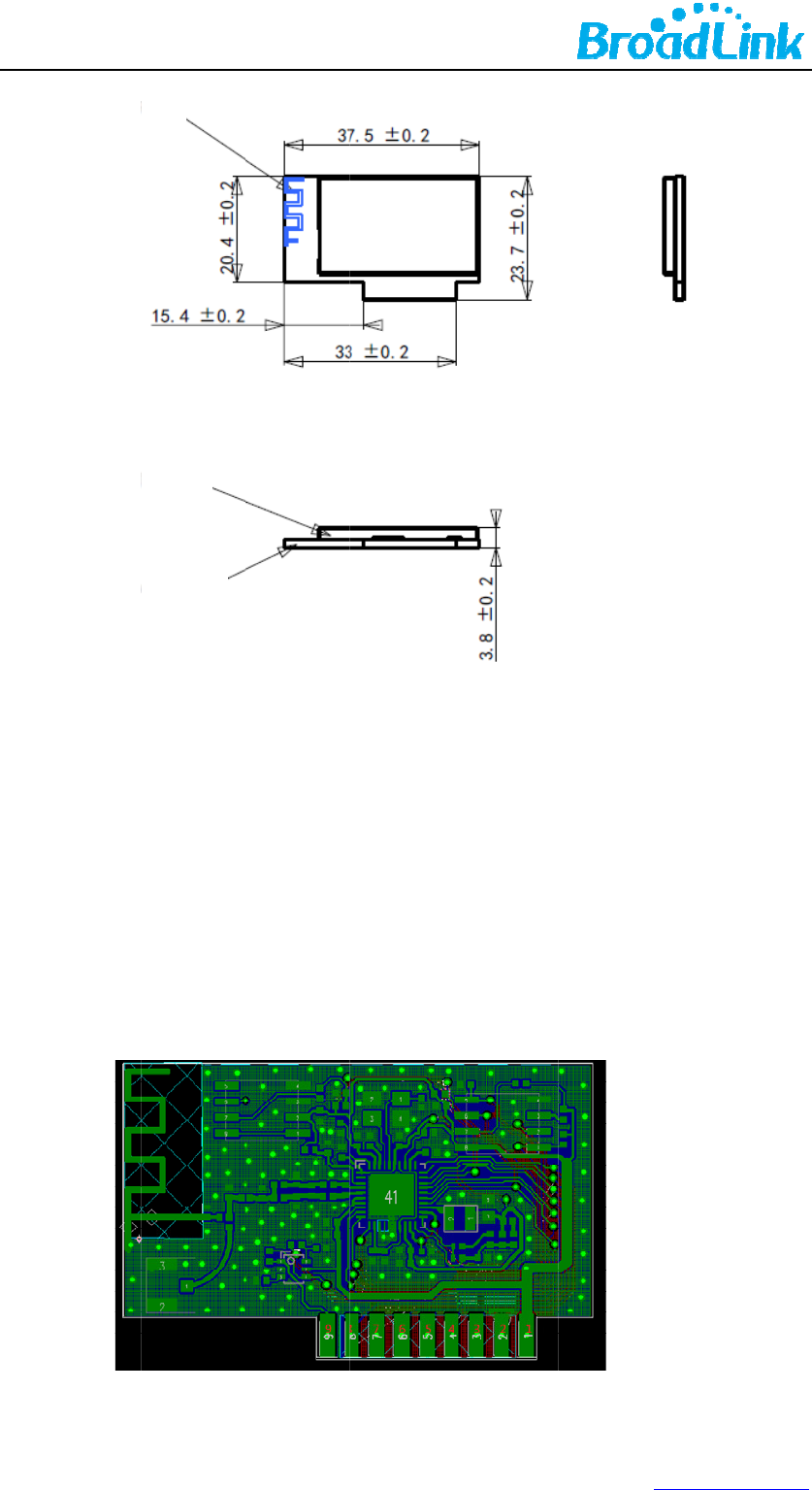
. Dimens
k. ESD: 2K
l. Absolu
t
Symbol
Ts
TAMBIEN
T
Vdd
Vio
VESD
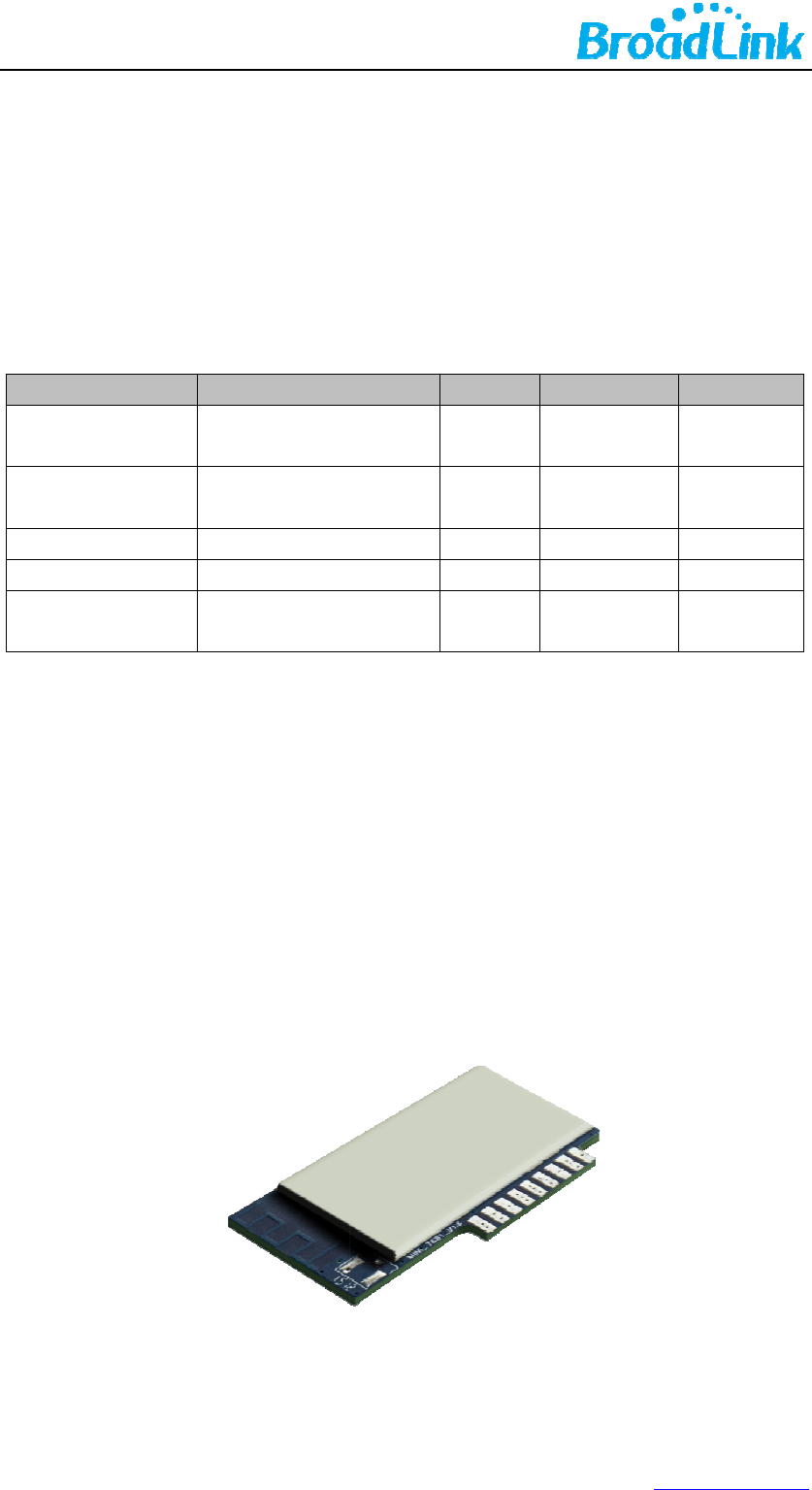
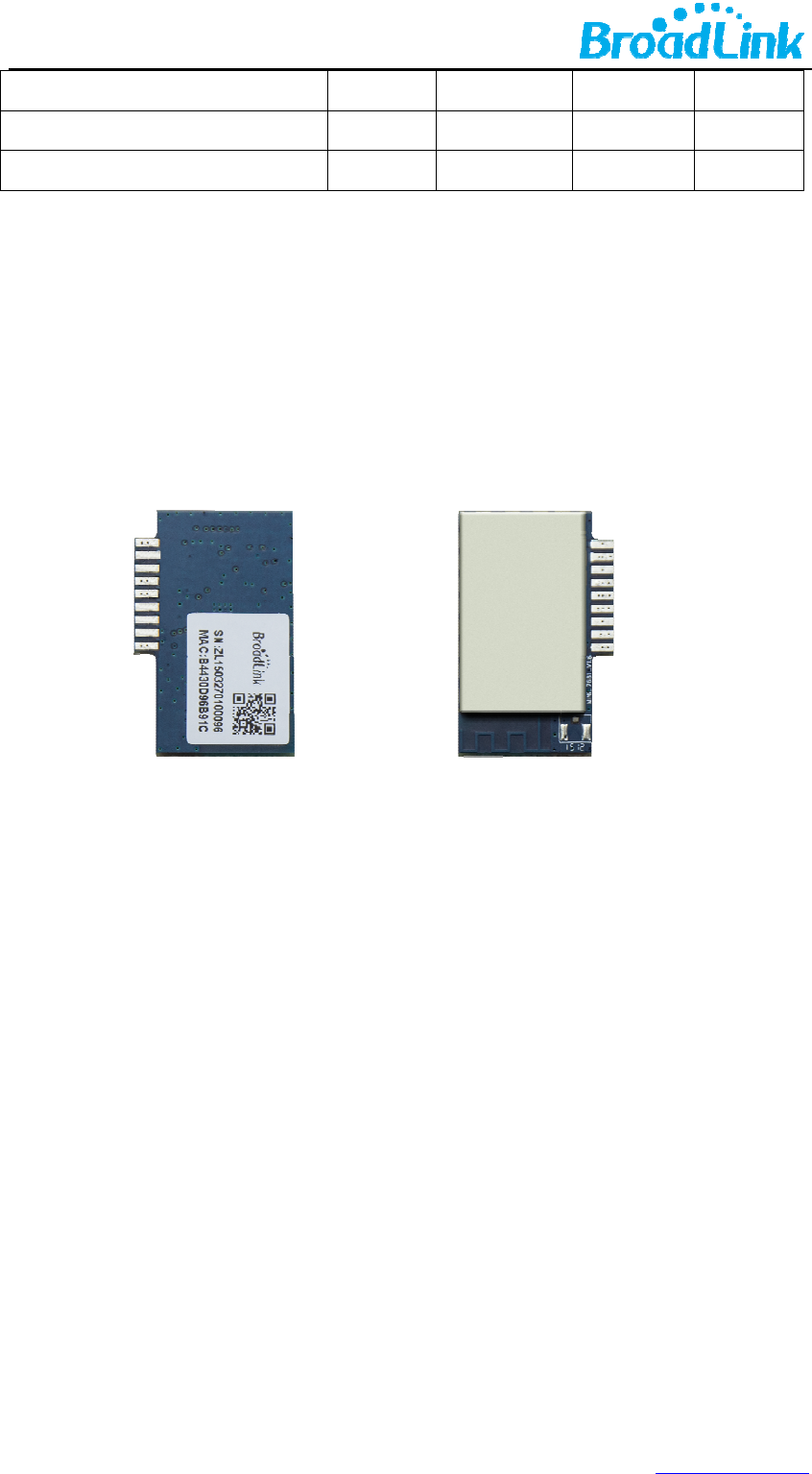
Produ
1
Produ
c
s
ource: 3.3V
rals:
T
O
ion 37.5mm
V
t
e maximum
St
o
T
A
m
V
H
ct Ove
c
t Pictu
r
*20.4mm*4
m
ratings
Descripti
o
o
rage temp
e
m
bient Tem
p
Supply vol
t
V
oltage on I
O
H
BM(human
model)
rview
r
e
m
m
o
n
e
rature
p
erature
t
age
O
pin
body
Min.
-40
-10
0
-0.28
5
w
Max.
125
70
3.63
3.63
2000
w
ww.ibroadlin
k
Units
℃
℃
V
V
V
k
.com

2.
2
3.
3.
1
Usi
n
the
the
s
peri
Sym
VD
D
VD
D
VD
D
2
Block
D
PCB
Antenna
Electr
i
1
Absolu
t
n
g products
device. Th
e
s
e conditio
n
ods may a
bol
D
33
D
12
D
15
D
iagra
m
Filter
Circuit
i
cal Ch
a
t
e Maxi
m
above the
e
se are ma
x
n
s is not i
m
ect the reli
a
Rating
3.3VSupply
V
1.2VSupply
V
1.5VSupply
V
m
Balun
Circuit
a
racte
r
m
um R
a
absolute m
x
imum ratin
g
m
plied. Exp
o
a
bility of the
M
V
oltage2
.
V
oltage1
.
V
oltage1
.
MT
802.
1
S
SPI
FLASH
40MHz
OSC
r
istics
a
tings –
aximum rat
g
s only an
d
o
sure to ma
device.
M
INTYP
.
973.3
.
141.2
.
4251.5
K7681
1
1 b/g/
n
S
oC
Multip
l
Circu
i
Voltag
e
ings may c
a
d
functional
ximum rati
n
M
3
1
1
6
w
n
l
ex
i
t
e
& Curr
e
a
use perma
n
operation
o
n
g conditio
n
M
AX
3
.63
1
.26
1
.575
w
ww.ibroadlin
k
UART
GPIO
e
nt
n
ent dama
g
o
f the devi
c
n
s for exte
n
Unit
V
V
V
k
.com
g
e to
c
e at
n
ded

3.
2
Ou
t
Sy
m
V
V
V
V
V
V
R
R
3.
3
Note
2
Digita
l
t
putvolta
g
m
bol
V
IL
V
IH
V
T- Sc
G
o
V
T+ P
o
V
OL
V
OH
O
R
PU In
R
PD Inp
u
3
Curren
t
Symbol
I
RF
I
RF
I
RF
I
RF
: All result is m
e
l
I/O Po
r
g
elevels
Param
e
Input Low
V
Input High
hmitt Trigg
e
o
ing Thresh
o
Schmitt
T
o
sitive Goin
g
Volta
g
Output Lo
w
O
utput Hig
h
put Pull-Up
u
t Pull-Dow
t
consu
m
RX
e
asured at the a
r
t Chara
e
ter
V
oltage
Voltage
e
r Negative
o
ld Voltage
T
rigger
g
Threshold
g
e
w
Voltage
h
Voltage
Resistance
n Resistanc
e
m
ption
Note
IDLE mo
Active, HT
4
TX HT40,
M
TX CC
K
ntenna port an
d
cteristi
c
Condi
t
LV
T
LV
T
|IOL| = 1.6
|IOH| =
1
m
A
PU=
h
PD=
e
PU=
l
PD=
h
de
4
0, MCS7
M
CS7
K
d
VDD33 is 3.3
V
c
s
t
ions
T
TL
-
T
TL
~14 mA
-
1
.6~14
A
h
igh,
low
l
ow,
h
igh
Cond
i
@ 15
d
11Mbps
@
V
7
w
MIN
-
0.28
2.0
0.68
1.36
-
0.28
2.4 VD
D
40
40
i
tion
d
Bm
@
18dBm
w
ww.ibroadlin
k
MAX
U
0.6
3.63
1.36
1.7
0.4
D
33+0.33
190
190
Perform
a
TYP
80
151
210
250
k
.com
U
nit
V
V
V
V
V
V
KΩ
KΩ
a
nce
Unit
mA
mA
mA
mA

3.
4
3.
5
S
V
E
S
4.
4.
1
O
p
Wi
M
o
Da
An
4.
2
M
o
4
Absol
u
Symbol
T
STG
T
A
Humidit
5
Absol
u
S
ymbol
S
D
(HBM)
RF Ch
a
1
Basic C
p
eratingFreq
u
-FiStandard
o
dulationTyp
ta Rates
tennatype
2
IEEE80
o
dulationTyp
u
te max
i
N
u
te max
i
Rati
n
Electrostati
c
discharge v
o
(human bo
d
a
racte
r
haracte
r
Item
u
ency
e
2.11b
M
Item
e
i
mum r
a
R
Storage
t
Working
on condensi
n
i
mum r
a
n
gs
c
o
ltage
d
y model)
r
istics
r
istics
M
ode
a
tings –
R
a
t
emperature
temperatur
e
n
g, relative h
u
a
tings –
Conditio
n
TA = +25 °
conformin
g
JESD22-A1
2.412 GH
z
IEEE 802.
1
11b: DBP
S
11g: BPS
K
11n: MCS
11b:1,2,5.
5
11g:6,9,1
2
11n:MCS
0
IPEX con
n
PCBprint
e
DSSS/CC
K
Temper
–
e
u
midit
y
ESD
n
s Class
C
g
to
14
2
Specificat
i
z
- 2.462 GH
z
1
1b/g/n
S
K, DQPSK,C
K
, QPSK, 16
Q
0~7,OFDM
5
and 11Mb
p
2
,18,24,36,48
0
~7,up to15
0
n
ectorforext
e
e
dANT
Specificat
i
K
8
w
ature
Max
–
40 to+125
-10 to+70
90%RH
Max
2000
i
on
z
CK for DSSS
Q
AM, 64QA
M
p
s
and 54 Mb
p
0
Mbps
e
rnalantenna
i
on
w
ww.ibroadlin
k
Uni
℃
℃
Unit
V
M
for OFDM
p
s
k
.com
t

Fr
e
Ch
Da
TX
C
Tra
n
11b
T
Fre
q
Co
n
1~1
RX
C
Mi
n
1M
b
2M
b
5.5
M
11
M
Ma
x
4.
3
M
o
Fr
e
Ch
Da
TX
C
Tra
n
11g
T
Fre
q
Co
n
6M
b
9M
b
12
M
e
quencyrang
e
annel
tarate
C
haracterist
n
smitter Ou
T
arget Powe
q
uency Erro
r
n
stellation E
r
1Mbps
C
haracteris
t
n
imum Inpu
t
b
ps (FE
R
≦8
%
b
ps (FE
R
≦8
%
M
bps (FE
R
≦
8
M
bps (FE
R
≦
8
x
imum Input
3
IEEE80
o
dulationTyp
e
quencyrang
e
annel
tarate
C
haracterist
n
smitter Ou
T
arget Powe
q
uency Erro
r
n
stellation E
r
b
ps
b
ps
M
bps
e
ics
tput Power
r
r
r
ror( peak E
t
ics
t
Level Sens
%
)
%
)
8
%)
8
%)
Level (FE
R
≦
2.11g
M
Item
e
e
ics
tput Power
r
r
r
ror( peak E
VM)@ targ
e
itivity
8%)
M
ode
VM)@ targ
e
2412MHz
CH1 toC
H
1,2,5.5,11
M
Min
T
-20
e
t power
Min
T
-20
-10
OFDM
2412MHz
CH1 toC
H
6,9,12,18,
2
Min
-20
e
t power
~2462MHz
H
11
M
bps
T
ypical
17
-17
T
ypical
-95
-93
-91
-89
Specific
a
~2462MHz
H
11
2
4,36,48,54
M
Typical
19
9
w
Max.
+20
-10
Max.
-83
-80
-79
-76
a
tion
M
bps
Max.
+20
-5
-8
-10
w
ww.ibroadlin
k
Unit
dBm
ppm
Unit
dBm
dBm
dBm
dBm
dBm
Unit
dBm
ppm
dB
dB
dB
k
.com

18
M
24
M
36
M
48
M
54
M
Tra
n
@1
1
@2
0
@3
0
RX
C
Mi
n
6M
b
9M
b
12
M
18
M
24
M
36
M
48
M
54
M
Ma
x
4.
4
TX
C
Tra
n
M
bps
M
bps
M
bps
M
bp
M
bps
n
smit spect
r
1
MHz
0
MHz
0
MHz
C
haracteris
t
n
imum Inpu
t
b
ps
b
ps
M
bps
M
bps
M
bps
M
bps
M
bps
M
bps
x
imum Input
4
IEEE80
Modulation
Frequencyr
a
Channel
Datarate
C
haracterist
n
smitter Ou
11n HT20
Frequ
e
r
um mask
t
ics
t
Level Sens
Level (FE
R
≦
2.11n 2
0
Item
Type
a
nge
ics
tput Power
Target Pow
e
e
ncy Error
itivity
10%)
0
Mhz B
a
er
Min
-
-20
a
ndwid
t
OFDM
2412MHz
CH1 toC
H
MCS0/1/
2
Min
-20
Typical
-90
-88
-86
-85
-82
-79
-75
-72
t
h Mod
e
Specific
a
~2462MHz
H
11
2
/3/4/5/6/7
Typical
19
10
w
-13
-16
-19
-22
-25
20
-28
-40
Max.
-83
-80
-79
-76
e
a
tion
Max.
+20
w
ww.ibroadlin
k
dB
dB
dB
dB
dB
dBr
dBr
dBr
Unit
dBm
dBm
dBm
dBm
dBm
dBm
dBm
dBm
dBm
Uni
t
dBm
pp
m
k
.com
t
m

Co
n
Tra
n
RX
C
Mi
n
M
a
n
stellation E
r
M
M
M
M
M
M
M
M
n
smit spect
r
@
1
@
2
@
3
C
haracteris
t
n
imum Inpu
t
M
M
M
M
M
M
M
M
a
ximum Inpu
r
ror( peak E
M
CS0
M
CS1
M
CS2
M
CS3
M
CS4
M
CS5
M
CS6
M
CS7
r
um mas
k
1
1MHz
2
0MHz
3
0MHz
t
ics
t
Level Sens
M
CS0
M
CS1
M
CS2
M
CS3
M
CS4
M
CS5
M
CS6
M
CS7
t Level (FE
R
≦
VM)@ targ
e
itivit
y
≦
10%)
e
t power
Min
-
-20
Typical
-89
-86
-84
-82
-78
-74
-72
-69
11
w
-5
-10
-13
-16
-19
-22
-25
-28
20
-28
-40
Max.
-82
-79
-77
-74
-70
-66
-65
-64
w
ww.ibroadlin
k
dB
dB
dB
dB
dB
dB
dB
dB
dBr
dBr
dBr
Uni
t
dBm
dBm
dBm
dBm
dBm
dBm
dBm
dBm
dBm
k
.com
t

4.
5
TX
C
Tra
n
Co
n
Tra
n
RX
C
Mi
n
5
IEEE80
Modulation
Frequencyr
a
Channel
Datarate
C
haracterist
n
smitter Ou
11n HT20
Frequ
e
n
stellation E
r
M
M
M
M
M
M
M
M
n
smit spect
r
@
1
@
2
@
3
C
haracteris
t
n
imum Inpu
t
M
M
M
M
M
M
2.11n 4
0
Item
Type
a
nge
ics
tput Power
Target Pow
e
e
ncy Error
r
ror( peak E
M
CS0
M
CS1
M
CS2
M
CS3
M
CS4
M
CS5
M
CS6
M
CS7
r
um mas
k
1
1MHz
2
0MHz
3
0MHz
t
ics
t
Level Sens
M
CS0
M
CS1
M
CS2
M
CS3
M
CS4
M
CS5
0
Mhz B
a
er
VM)@ targ
e
itivit
y
a
ndwid
t
OFDM
2422MHz
CH3 toC
H
MCS0/1/
2
Min
-20
e
t power
Min
-
t
h Mod
e
Specific
a
~2452MHz
H
9
2
/3/4/5/6/7
Typical
19
Typical
-89
-86
-84
-82
-78
-74
12
w
e
a
tion
Max.
+20
-5
-10
-13
-16
-19
-22
-25
-28
20
-28
-40
Max.
-82
-79
-77
-74
-70
-66
w
ww.ibroadlin
k
Uni
t
dBm
pp
m
dB
dB
dB
dB
dB
dB
dB
dB
dBr
dBr
dBr
Uni
t
dBm
dBm
dBm
dBm
dBm
dBm
k
.com
t
m
t
M
a
5.
M
M
a
ximum Inpu
Mech
a
M
CS6
M
CS7
t Level (FE
R
≦
a
nical
C
≦
10%)
C
harac
t
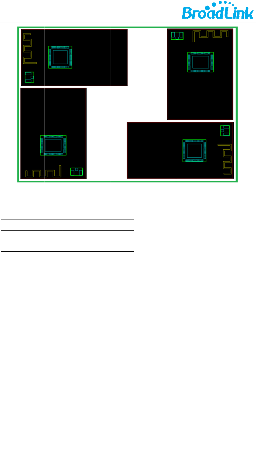
Figu
-20
t
eristi
c
re2.
WT1FBS
-72
-69
c
s
13
w
-65
-64
w
ww.ibroadlin
k
dBm
dBm
dBm
k
.com
6.
6.
1
WT
1
Modu
1
PIN La
y
1
FBS has on
Anten
Shieldin
WiF
i
le Inte
r
y
out
e group of
p
na
gCase
i
Module
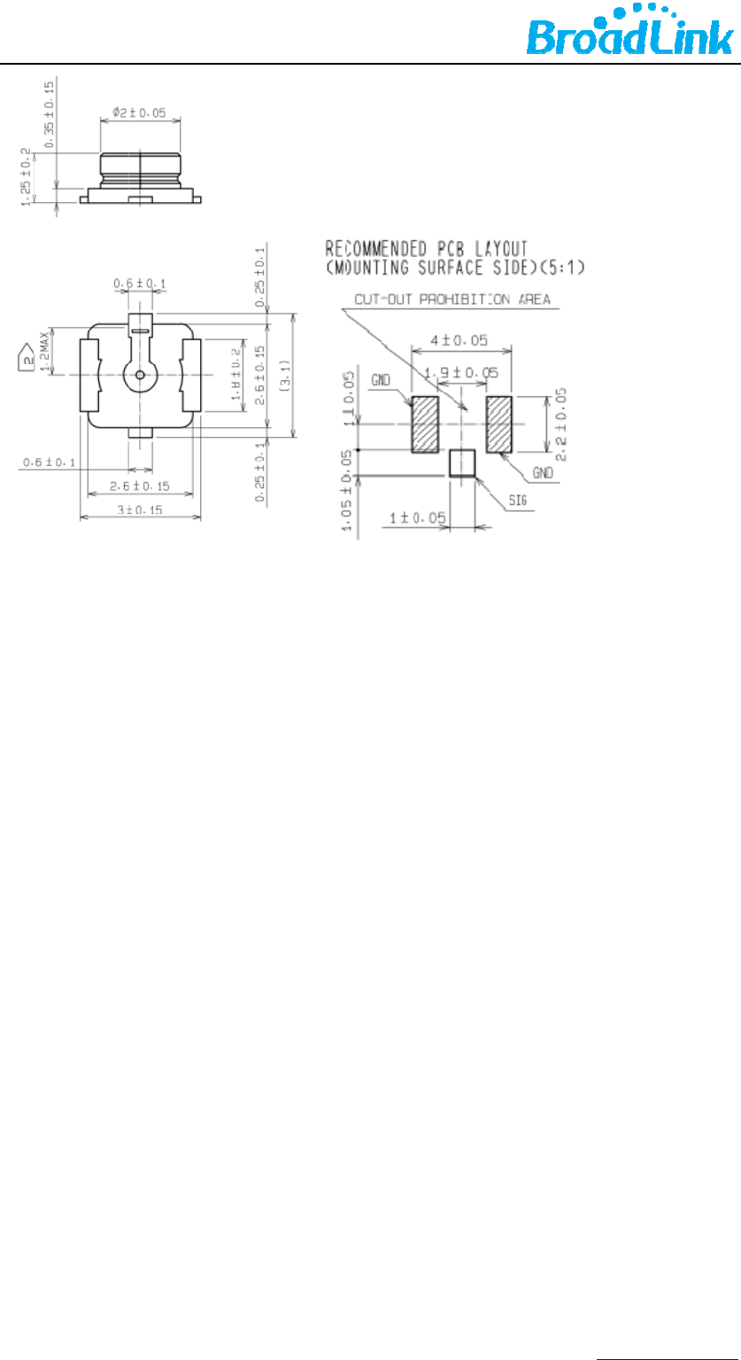
Figure3.
W
T
r
faces
p
ins1X9. Th
e
T
1FBS
view(
M
e
layout of
P
M
etricun
it
s
)
P
INs are sho
w
14
w
w
n in the fi
g
w
ww.ibroadlin
k
g
ure belo
w
.
k
.com

6.
2
PI
N
PIN
Pin
1
Pin
2
Pin
3
Pin
4
Pin
5
Pin
6
Pin
7
Pin
8
Pin
9
2
PIN D
e
N
Assignm
e
1
2
3
4
5
6
7
8
9
e
finitio
n
e
nt
Figure6.
W
T
n
s
PINNA
M
VDD
GND
GPIO0
GPIO1
GPIO2
GPIO3
GPIO0
UART_T
X
UART_R
X
T
1FBS
pin-ou
t
M
E
X
X
t
N
S
O
15
w
N
OTE
S
oftRest;Hi
g
O
nlyfortran
s
w
ww.ibroadlin
k
g
hLevelOn
s
parenttran
s
k
.com
s
fer
7.
For
be
c
The
sho
u
filte
tha
t
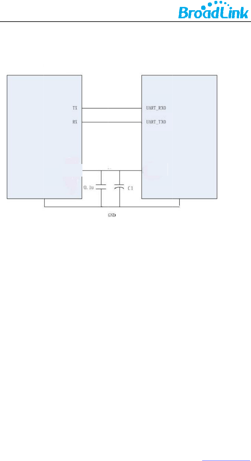
Refer
e
the devices
c
onnected d
WT1FBS us
u
ld be mo
r
ring capacit
t
the value
o
UserEqui
p
e
nce D
e
using pow
e
irectly as th
es power s
o
r
e than 30
0
or and recti
f
o
f C1 is not l
e
p
ment
3.3
v
e
sign
e
r source of
3
e picture a
b
o
urce of 3.3
V
0
mA. The V
D
f
ication cap
a
e
ss than 10
0
v
3
3
.3V, the U
A
b
ove to start
V
. It is reco
m
D
D power
s
a
citor to en
s
0
uF.
3
.3v
A
RTs of host
d
communic
a
m
mended th
s
upply is c
o
s
ure voltage
WiFiMo
d
3.3v
16
w
d
evice and
W
a
ting.
at the pow
e
o
nnected i
n
stability. It i
d
ule
w
ww.ibroadlin
k
W
iFi modul
e
e
r supply cu
n
parallel w
i
s recomme
n
k
.com
e
can
rrent
i
th a
n
ded
8.
8.
1
The
bet
w
Anten
1
Anten
n
WT1FBS su
w
een 2.4G~
2
In practical
changes.
When cho
o
naCha
r
n
a Selec
pports on-
b
2
.5GH, S11
o
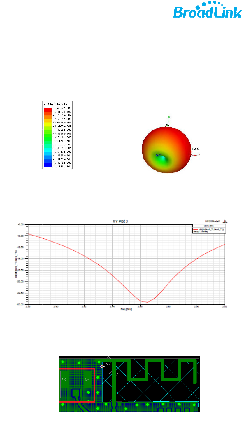
Figu
F
use, WT1F
B
o
se the exte
r
acteri
tion
b
oard PCB p
o
f antenna
p
r
e 7. Antenn
F
igure 8. Ant
B
S is welded
rnal antenn
a
stics
rinted ante
n
p
ort is less t
a radiation
p
enna port S
1
on user’s b
a
, it needs t
o
n
na.When t
h
han-10dB a
n
p
attern simul
1
1simulation
oardand val
o
move the
17
w
h
e Operatin
g
n
d peak gai
ation
curve
ue of S11 h
a
resistance f
r
w
ww.ibroadlin
k
g
Frequency
nis about 2
d
a
s some
r
om the loc
a
k
.com
is
d
Bi.
a
tion
of L
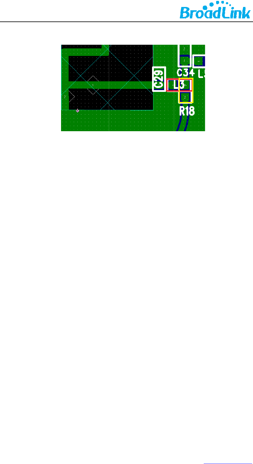
8.
2
Wh
e
thr
e
1.
T
co
m
sig
n
2. T
h
boa
3.
W
mo
d
ant
e
3 to R18, as
2
Minim
e
n integrati
n
e
e points be
l
T
he area u
n
m
ponents, c
o
n
al.
h
e area aro
u
rd PCB and
W
hen planni
d
ule as clos
e
nna, which
shown in t
h
izing R
a
n
g the Wi-F
i
l
ow:
n
der the an
o
nnectors, v
u
nd the ant
e
any metal e
ng PCB lay
o
e as possib
l
is shown in
h
e red recta
n
a
dio Int
e
i
module wi
t
tenna end
ias, traces a
e
nna end th
e
nclosure.
o
ut, it is re
c
l
e to the ed
the picture
n
gle of the
p
e
rferenc
t
h on board
of the mo
d
nd other m
a
e
module p
r
c
ommende
d
ge of boar
d
below.
p
icture belo
w
e
PCB printe
d
d
ule should
a
terials that
r
otrudes at l
e
d
that user
p
d
er to ensu
r
18
w
w
.
d
antenna,
m
be keep
c
can interfe
r
e
ast 10mm
f
p
laces the
a
r
e the good
w
ww.ibroadlin
k
m
ake sure th
c
lear of me
r
e with the
r
f
rom the m
o
a
ntenna of
W
performan
c
k
.com
e
tallic
r
adio
o
ther
W
i-Fi
c
e of
8.
3
O
p
VS
W
Pe
a
An
8.
4
3
Specif
i
p
eratingFreq
u
W
R(max)
a
k Gain
tennaType
4
IPEX C
i
cation
o
u
ency 2.4
G
2
2dB
i
IFA
onnect
o
o
f On-B
o
G
~2.5GHz
i
o
r
o
ard An
t
t
enna
19
w
w
ww.ibroadlin
k
k
.com
20
w
w
ww.ibroadlin
k
k
.com

A
p
AD
C
AE
S
AN
T
AP
BP
S
DB
P
DC
CC
K
CD
M
DH
C
CM
O
DN
S
DQ
P
DS
S
DTI
EM
S
ES
D
EV
M
FC
C
FE
R
GN
D
GPI
HB
M
IEE
E
IO
IOT
IPv
4
LE
D
LV
T
MA
MC
S
MC
U
MI
M
MS
L
NC
NR
S
OF
D
OS
C
PC
B
PIF
A
QP
S
p
pendi
C
S
T
S
K
P
SK
K
M
C
P
O
S
S
P
SK
S
S
M
S
P
D
M
C
R
D
O
M
E
4
D
T
TL
C
S
U
M
O
L
S
T
D
M
C
B
A
S
K
x A
Analo
g
Advan
Anten
n
Wirel
e
Binar
y
Differ
e
Direct
Comp
l
Charg
e
Dyna
m
Comp
l
Deter
m
Differ
e
Dema
n
Digital
Enhan
c
Electr
o
Error
V
Feder
a
Floatin
Groun
d
Gener
a
Huma
n
Institu
t
Input/
o
Individ
Intern
e
Light-
e
Low V
o
Mediu
m
Modul
Micro
c
Multip
Multil
a
Nume
r
Negati
Ortho
g
Oscill
a
Printe
d
Planar
Quadr
a
g
‐to‐Digital
cedEncryp
t
n
a
e
ssAccess
P
y
PhaseShif
t
e
ntial binar
y
Current
l
ementary
C
e
DeviceM
o
m
ic Host Co
n
l
ementary
M
m
ination of
n
e
ntial quadr
a
n
d assigned
Transmissi
o
c
ed Modula
o
static Disch
a
V
ector Magn
a
l Communi
c
g Error
d
a
l Purpose I
n
n
body mod
t
e of Electri
c
o
utput
ual operati
o
e
t Protocol
v
e
mitting dio
d
o
ltage Trans
m
Access C
o
ation and c
o
c
ontroller U
n
le-Input Mu
a
yer Switchi
n
r
ical Control
ve Reset
g
onal Frequ
e
a
to
r
d
Circuit Bo
a
inverted F
a
a
ture Phase
Converter
t
ionStand
a
P
oint
t
Keying
p
hase shift
C
odeKeyin
g
o
del
n
figuration
P
M
etalOxid
e
n
on-signific
a
a
ture phase
signaling a
n
o
n Interface
r Signal Pro
c
a
rge
itude
c
ations Co
m
n
put/Outpu
t
el
c
al and Elec
t
o
n test
v
ersion 4
d
e
istor Logic
o
ntrol layer
o
ding sche
m
n
it
ltiple-Outp
u
n
g Protocol
e
ncy Divisio
a
rd
a
ntenna
Shift Keyin
a
rd
ke
y
in
g
g
P
rotocol
e
Semicond
u
a
nce
shift keying
n
d switchin
g
Module
c
essor
m
mission
t
t
ronics Engi
n
m
e
u
t
n Multiplexi
21
w
u
ctor
g
subsystem
n
eers
ng
w
ww.ibroadlin
k
k
.com

RC
RF
RIS
C
Ro
H
RX
SDI
O
So
C
SP
D
SPI
ST
A
TC
P
TKI
P
T
X
IP
UA
R
UD
P
UF
L
VS
W
WE
P
WE
P
WE
P
WE
P
WP
A
XT
A
QA
M
80
2
C
H
S
O
C
D
T
A
P
P
R
T
P
L
W
R
P
P
A
P
64
P
128
A
2
A
L
M
2
.11 b/g/n
Resist
a
Radio
F
Reduc
e
Restric
Receiv
e
Serial
D
Syste
m
Single
-
Serial
P
Spann
i
Transf
e
Temp
o
Trans
m
Intern
e
Univer
s
User
D
a mi
n
manuf
a
Voltag
e
Wired
Welde
d
64 bit
128 bi
t
Wi-Fi
P
Extern
a
Quadr
a
The IE
E
a
nce- capaci
F
requency
e
d Instructi
o
tion of Haz
a
e
r
D
igital Inpu
t
m
on Chip
-
Pole Doubl
e
P
eripheral I
n
i
ng Tree Alg
e
r Control P
r
o
ral Key Inte
g
m
itter
e
t Protocol
s
al Asynchr
o
D
atagram Pr
o
n
iature coa
a
ctured by
H
e
Standing
W
Equivalent
P
d
Electronic
Wired Equ
t
Wired Eq
P
rotected A
c
a
l Crystal O
s
a
ture Ampli
t
E
E 802.11 b
/
tance
o
n Set Com
p
a
rdous Subs
t
/Output
e
-Throw
n
terface
orithm
r
otocol
g
rity Protoc
o
o
nous Recei
v
o
tocol
xial RF c
H
irose Elect
W
ave Ratio
P
rivacy
Packaging
A
ivalent Priv
a
uivalent Pri
v
c
cess 2
s
cillator
t
ude Modul
a
/
g/n
p
uter
tances
o
l
v
er/Transmi
t
onnector f
o
ric Group
A
ssociation
a
cy
v
acy
a
tion
22
w
t
ter
o
r high-fre
q
w
ww.ibroadlin
k
q
uency si
g
k
.com
g
nals
A
p
[1]
pu
b
pu
b
802
F
C
A
ny
cou
l
the
cau
s
incl
u
FC
C
p
pendi
IEEE 802.1
b
lished IEEE
b
lishedIEEE
.11-2012 st
a
C
C WA
Changes o
r
l
d void the u
FCC Rules.
s
e harmful
u
ding interfe
r
C
Radiatio
n
x B
1b/g/n- p
u
802.11-201
802.11-20
0
a
ndard.
RNIN
G
r
modificatio
n
ser’s author
Operation i
s
interference
,
r
ence that
m
n
Exposur
e
u
blished IE
E
2 standard
0
7 standard
G
S:
n
s not expre
s
ity to operat
e
s
subject to
t
,
and (2) t
h
m
ay cause u
n
e
Stateme
n
E
E 802.11-
2
for Inform
a
, and
C
s
sly approv
e
e
the equip
m
t
he following
h
is device
m
n
desired ope
r
n
t:
2
007wireles
s
a
tion techn
C
lause 19
e
d by the par
t
m
ent.This d
e
two conditi
o
m
ust accept
r
ation.
23
w
s
networkin
ology - Cl
a
of the
t
y responsib
e
vice compli
e
o
ns: (1) Thi
s
any interfe
r
w
ww.ibroadlin
k
g standard
a
use 19 o
f
published
le for compli
e
s with part
1
s
device ma
y
r
e nce rece
k
.com
and
f
the
IEEE
ance
1
5 of
y
n ot
ived,

Thi
s
env
i
bet
w
con
j
fou
n
Rul
e
in a
ene
r
inte
r
occ
u
tele
v
enc
o
—R
—I
n
—C
con
n
—C
In
a
dev
i
Tec
h
co
m
doc
u
FC
C
The
refe
foll
o
2A
C
To
s
sep
a
dev
i
dist
a
or o
s
equipment
i
ronment. T
h
w
een the rad
j
unction with
n
d to comply
e
s. These li
m
residential i
n
r
gy and, if n
o
r
ference to r
a
u
r in a partic
v
ision recep
t
o
uraged to t
r
eorient or re
n
crease the
s
onnect the
e
n
ected.
onsult the d
e
a
ccordance
w
i
ce.Therefor
e
h
nologyCo.,
m
pliancewit
h
u
mentedint
C
Label Instr
u
outside of fi
rring to the
e
o
wing: “Cont
a
C
DZ-WT1FB
S
s
atisfy FCC
R
a
ration dist
a
i
ce and per
s
a
nce is not r
e
perating in
c
complies wi
t
h
is equipme
n
iator& your
b
any other a
n
with the limi
m
its are desi
g
n
stallation.
T
o
t installed a
a
dio commu
n
ular installat
i
t
ion, which c
a
r
y to correct
locate the r
e
s
eparation b
e
e
quipment in
t
e
aler or an e
w
ith FCC P
a
e
,thefinal
h
Ltd.]forco
n
h
theregula
heFilingisu
s
u
ctions
nal product
s
e
nclosed mo
d
a
ins Transm
i
S
” Any simil
a
R
F Exposur
e
a
nce of 20
c
s
ons during
e
commende
c
onjunction
w
t
h FCC radi
a
n
t should be
i
b
ody. This tr
a
n
tenna or tr
a
ts for a Clas
g
ned to prov
i
T
his equipm
e
nd used in
a
n
ications. H
o
i
on. If this e
q
a
n be deter
m
the interfere
e
ceiving ant
e
e
tween the
e
t
o an outlet
o
xperienced
r
a
rt 15C, thi
s
h
ostproduc
t
n
firmationt
h
tionsofFC
C
s
ed,aClass2
s
that contai
n
d
ule. This e
x
i
tter Module
a
r wording t
h
e
requireme
n
c
m or more
operation.
T
d. The ante
n
w
ith any othe
a
tion exposu
r
i
nstalled an
d
a
nsmitter m
u
a
nsmitter. N
o
s B digital d
e
i
de reasona
b
e
nt generate
s
a
ccordance
w
o
wever, ther
e
q
uipment do
e
m
ined by tur
n
nce by one
o
e
nna.
e
quipment a
n
o
n a circuit d
r
adio/TV tec
h
s
module is
t
mustbes
u
h
attheinst
a
C
.Specificall
Permissive
C
n
s this modu
l
x
terior label
c
FCC ID: 2A
C
h
at expresse
n
ts for mobil
e
should be
m
T
o ensure c
n
na(s) used
f
r antenna o
r
r
e limits set
f
d
operated w
u
st not be c
o
o
te: This equ
e
vice, pursu
a
b
le protectio
n
s
uses and
c
w
ith the instr
u
e
is no guar
a
e
s cause ha
r
n
ing the equ
i
o
r more of th
n
d receiver.
ifferent from
h
nician for h
e
listed as a
u
bmittedto
a
llationofth
y,ifanan
t
C
hangemust
l
e device m
u
c
an use wor
d
C
DZ-WT1F
B
s the same
m
e
and base s
t
m
aintained
b
ompliance,
o
f
or this trans
r
transmitter.
24
w
f
orth for an u
ith minimum
o
-located or
o
ipment has
b
a
nt to part 1
5
n
against ha
r
c
an radiate r
a
u
ctions, ma
y
a
ntee that int
r
mful interfe
r
i
pment off a
n
e following
m
that to whic
h
e
lp.
Single Mo
d
[HangZhou
G
emodulei
n
t
ennaother
befiledwith
u
st display a
d
ing such a
s
B
S” or “Cont
a
m
eaning ma
y
t
ation trans
m
b
etween th
e
o
peration at
mitter must
n
w
ww.ibroadlin
k
u
ncontrolled
distance 20
o
perating in
b
een tested
5
of the FC
C
r
mful interfer
a
dio frequen
c
y
cause har
m
t
erference wi
r
ence to radi
o
n
d on, the u
s
m
easures:
h
the receiv
e
d
ular Trans
m
G
ubeiElectr
o
n
tothehost
thanthe
m
theFCC.
label
s
the
a
ins FCC ID:
y
be used.
m
ission devic
e
antenna o
f
closer tha
n
n
ot be co-lo
c
k
.com
cm
and
C
ence
c
y
m
ful
ll not
o
or
s
er is
e
r is
m
itter
o
nics
isin
m
odel
es, a
f
this
n
this
c
ated

C
o
Ha
n
Ro
o
T: +
E: i
n
o
ntact
n
gzhou G
u
o
m 106, Buil
d
86-571-85
1
n
tl@broadli
n
Us
u
bei Elect
d
ing 1, No.
6
1
59281
n
k.com.cn
ronics Te
c
6
11 Jiangho
F: +86-5
7
W: www.i
c
hnology
C
ng Road, Bi
n
7
1-8663181
7
broadlink.c
o
C
o., Ltd.
n
jiang, Han
g
7
o
m.cn
25
w
g
zhou, Zheji
w
ww.ibroadlin
k
ang, P.R.Chi
n
k
.com
n
a