Hangzhou Tuya Information Technology TYBT3 BLE Module User Manual TYBT2 EN V1x
Hangzhou Tuya Information Technology Co.,Ltd BLE Module TYBT2 EN V1x
User Manual
TYBT3 DATASHEET
Tuya Smart BLE Module
1. Product Overview
TYBT3 is a Bluetooth (BLE) module designed by Hangzhou Tuya Information Technology
Co., Ltd. The BLE Module consists of a highly integrated wireless Bluetooth chip TLSR8267 and
some extra electric circuits that have been programed with Bluetooth network protocol and plenty
of software examples.TYBT3 include a 32-bit CPU, BLE, 512K byte flash, 16k SRAM, and 9
multiplex IO pins.
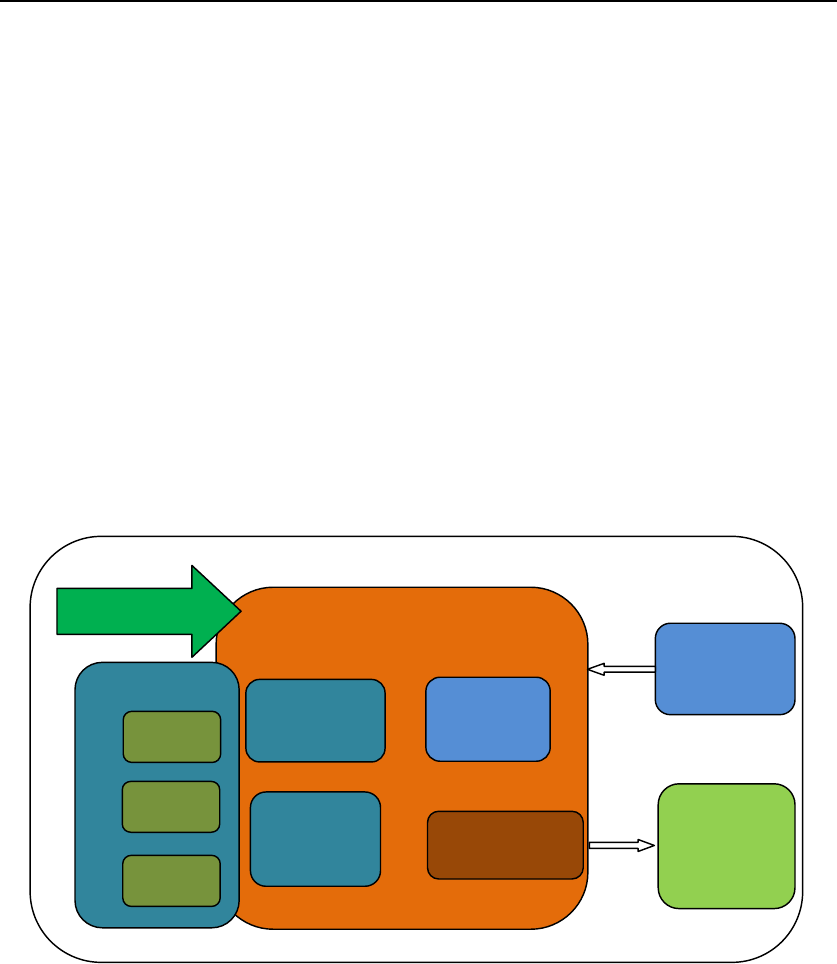
Figure 1 shows the block diagram of the TYBT3.
Figure 1. The block diagram of the TYBT3
1.1 Features
Integrated low power consumption 32-bit CPU, also known as application processor
Basic frequency of the CPU can support 48 MHz
Supply voltage range: 1.9V to 3.6V
Peripherals: 5*PWM,1*I2C, 1*UART
BLE RF features:
Compatible with BLE 4.2
Transmitting data rate can go up to 1Mbps
TX transmitting power: +6.06dBm
RX receiving sensitivity: -92dBm
AES hardware encryption
On-board PCB antenna
BLE
IO interface
12M
Crystal
PCB
on-board
antenna
BLE
MCU FREQ
48MHz
SRAM
16K Bytes
FLASH
512K
I2C
3.3V input
PWM
UART

TYBT3 DATASHEET
Operating temperature range: -20℃ to 85℃
1.2 Main Application Fields
Intelligent LED
Intelligent household applications
Intelligent low-power consumption sensors
TYBT3 DATASHEET
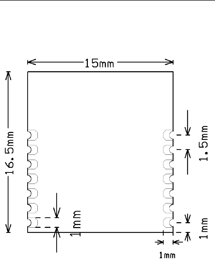
2. Dimensions and Footprint
2.1Dimensions
TYBT3 have double sides of pins. The distance between each Pin is 2.0mm.
Size of TYBT3: 15mm(W)*16.5mm(L).
Figure 2 shows the dimensions of TYBT3.
Figure 2. The dimensions of TYBT3
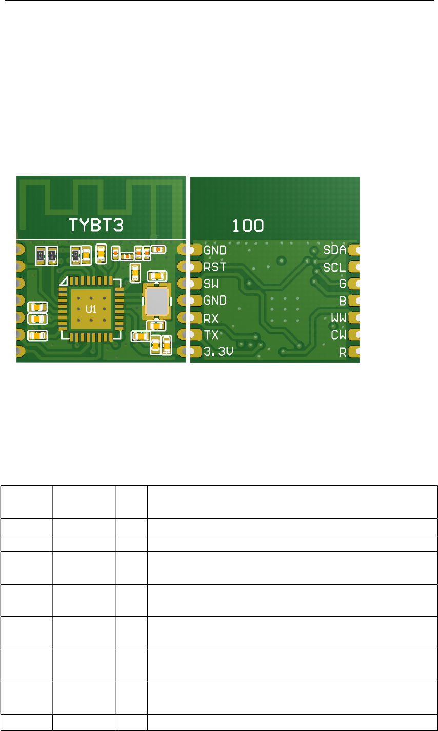
2.2 Pin Definition
Table 1 shows the general pin attributes of TYBT3
Table 1. The typical pin definition of TYBT3
PIN NO. NAME TYP
E
DESCRIPTION
1 SDA I/O I2C, data interface,internal pull-up 4.7k resistance
2 SCL I/O I2C, clock interface, internal pull-up 4.7k resistance
3 G I/O normal IO pin, can be used as PWM output pin, default for
Green LED line
4 B I/O normal IO pin, can be used as PWM output pin, default for Blue
LED line
5 WW I/O normal IO pin, can be used as PWM output pin, default for
Warm White LED line
6 CW I/O normal IO pin, can be used as PWM output pin, default for Cold
White LED line
7 R I/O normal IO pin, can be used as PWM output pin, default for Red
LED line
8 3.3V P Supply voltage

TYBT3 DATASHEET
9 TX I/O UART TX,can be used as normal IO pin
10 RX I/O UART RX,can be used as normal IO pin
11 GND P Ground
12 SW I/O Bluetooth chipset burning pin
13 RST I reset pin for the module,internal pull-up 4.7k resistance
14 GND P Ground
Note: P: Power supply pins; I/O: Digital input or output pins.
SW pin is ONLY used for burning firmware, Can NOT be used for other functions.
There are 4.7 pull-up resistance internally for I2C pins, external pull-up resistances are not
necessary.
When WW pin is outputting PWM signal, It has opposite phase comparing the PWM signal
from R/G/B/CW pin.
If there’s any customization needed for PWM output, please contact our BD manager.
TYBT3 DATASHEET
3. Electrical Characteristics
3.1 Absolute Maximum Ratings
Table 2. Absolute Maximum Ratings
PARAMETERS DESCRIPTION MIN MAX UNIT
Ts Storage
temperature
-20 85 ℃
VCC Supply voltage -0.3 3.9 V
Electrostatic release quantity
(Human body model)
TAMB-25℃ - 2 KV
Electrostatic release quantity
(Machine model)
TAMB-25℃ - 0.5 KV
3.2 Electrical Conditions
Table 3. Electrical Conditions
PARAMETERS DESCRIPTION MIN TYPIC
AL
MAX UNIT
Ta Temperature for Commercial grade -20 - 85 ℃
VCC Supply voltage
VIL IO negative level input
VIH IO positive level input
VOL IO negative level output
VoH IO positive level output
3.3Transmitting Current Consumptions
Table 4. TX current consumption
PARAMETERS MODE TYPICAL UNIT
Itx Continuously transmitting, 0dBm power output
Irx Continuously receiving
IDC Normal working mode
1.9 3.3 3.6 V
-0.3 - VCC*0.3 V
VCC*0.7 - VCC V
VSS - 0.3 V
VCC-0.3 - VCC V
15 mA
12 mA
27 mA
18 uA
Ideepsleep Sleep mode
TYBT3 DATASHEET
4. Radio Specification
4.1 Basic Radio Frequency Characteristics
Table 5.Basic Radio frequency characteristics
PARAMETERS DESCRIPTION
Working Frequency 2.4GHz ISM band
Radio standard BLE 4.2
Data transmitting rate
Type of Antenna On-board PCB Antenna
4.2Transmitting Power
Table 6. Transmitting power
PARAMETERS MIN TYPICAL MAX UNIT
RF Average output power
consumption
5.46 5.70 dBm
4.3Receiving Sensitivity
Table 7. Receiving sensitivity
PARAMETERS MIN TYPICAL MAX UNIT
RX sensitivity
Frequency bias error
Co-channel interference Restrain - - -7 - dB
1Mbps
6.06
1Mbps -93 -92 -90
dBm
1Mbps -300 - +300
KHz
weld TYBT3 module and other electrical
5. An
tenna Information
5.1 Antenna Type
e is
5.2 Reduce Antenna I
nterference
st
rt and the other metal pieces.
Since PCBA
manufacture use
c
omponents onto the PCB board, RF performance will depend on the layout location and patt
of the On-
board PCB antenna. The following figures are some recommended and
dis-recommended de
monstrations from out R&D team.
In demonstration 1
and 2 of figure 3, the on
frame. I
t’s recommended to use layout pattern shown in
on-board PCB antenna lays
outside of the PCB frame directly or PCB frame
area for the antenna. The o
verall PCBA
t
esting the module independently.
R
estricted due to some reason, i
frame, it’s suggested to refe
r to demonstration 3.
copperor wire beneath t
he antenna.
I
t’s NOT recommended to use demonstra
t
here are copper and wire beneath it. RF performance will have
De
monstration 1: Antenna lay outside the
P
CB frame
TYBT3 DATASHEET
Antenna Information
m
nte
rference
n order to have the
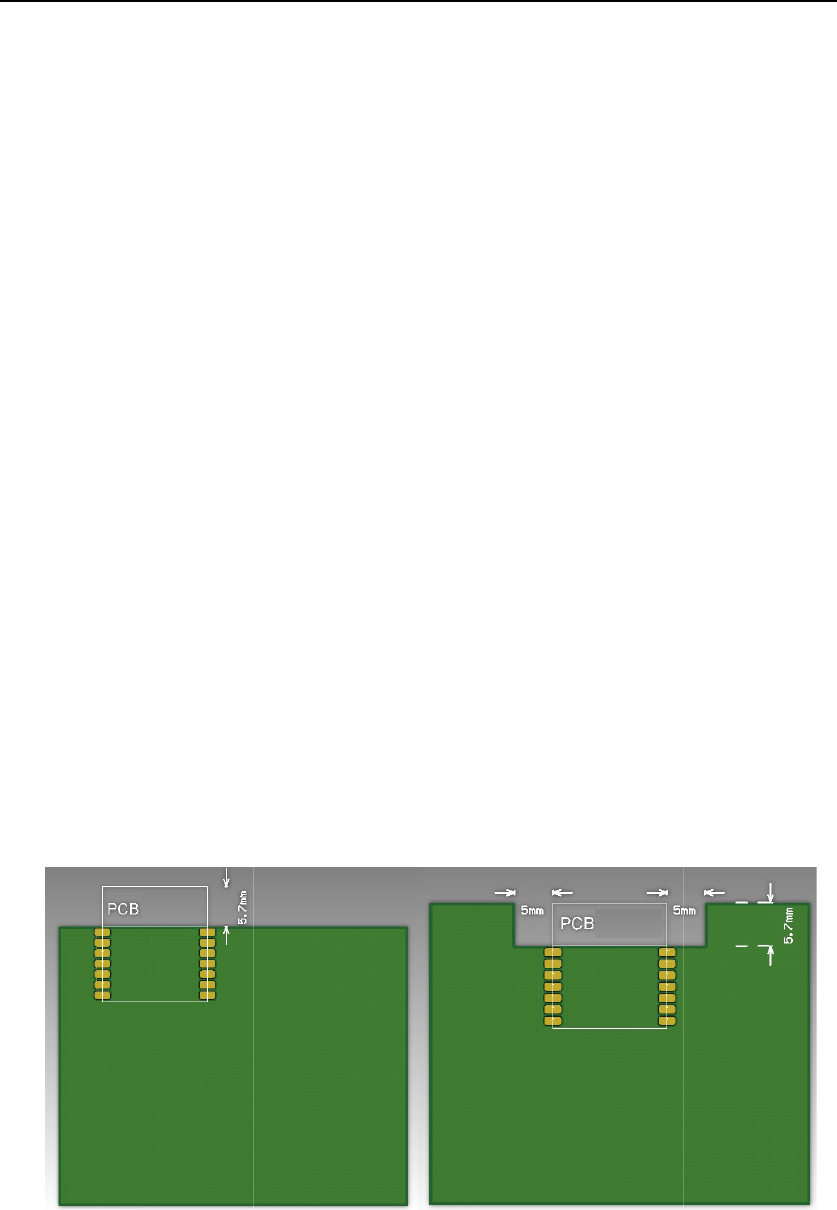
In order to have the best RF performance, it’s recommended to keep a minimum
between the ante
15mm distance between the antenna nna pa part and the other metal pieces.
A manufacture use
SMT process to we
ld TYBT3 module and other electrical
components onto the PCB board, RF performance will depend on the layout location and patt
board PCB antenna. The following figures are some recommended and
demonstrations from out R&D team.
1 and 2 of figure 3, the on
-board PCB antenna lays
outside
It’s recommended to use layout pattern shown in
demonstration 1
and 2. Either the
out
side of the PCB frame directly or PCB frame c
ar
overall PCBA
performance for
these two ways will be the same as
testing the module independently.
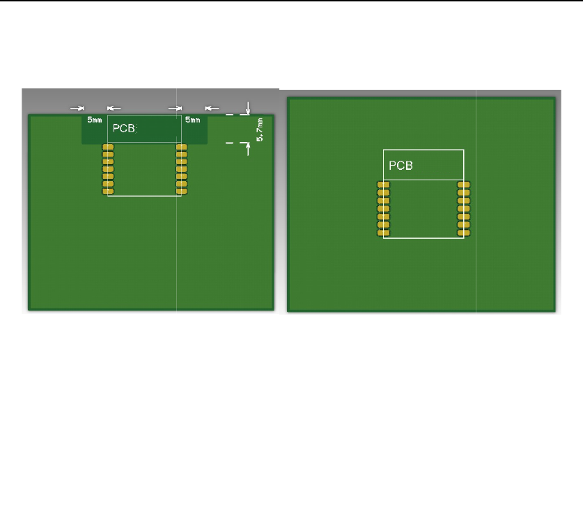
Restricted due to some reason, i
f the on-board PCB antenna layout
has to be inside the PCB
er to demonstration 3.
The ante
nna lays inside the PCB frame,
the antenna.
R
F performance will have some loss, approximately 1~2 dBm.
It’s NOT recommended to use demonstra
tion 4, the antenna l
ays inside the PCB frame, and
there are copper and wire beneath it. RF performance will have
tion
Figure 3.layout demostrations
Demonstration 1: Antenna lay outside the
PCB frame
De
monstration 2: Antenna lay
t
he PCB frame with carved area
Antenna for TYBT3
modulodule is using 2.4 GHz MIFA On-board PCB antenna.
to keep
components onto the PCB board, RF performance will depend on the layout location and patt
ern
board PCB antenna. The following figures are some recommended and
out
side of the PCB
1 and 2. Either the
car
ve out a certain
for these two ways will be the same as
ut has to be inside the PCB
enna lays inside the PCB frame,
but no
RF performance will have some loss, approximately 1~2 dBm.
lays inside the PCB frame, and
atte
significant attenuanuation.
Demonstration 2: Antenna lay
outside
the PCB frame with carved area
De
monstration 3: Antenna lay inside the PCB
frame w
ithout copper or wire beneath it
TYBT3 DATASHEET
Demonstration 3: Antenna lay inside the PCB
without copper or wire beneath it
De
monstration 4: Antenna lay inside the PCB
f
rame with copper or wire beneath it
Demonstration 4: Antenna lay inside the PCB
frame with copper or wire beneath it
TYBT3 DATASHEET
6. Packaging Information And Production Guide
6.1 Mechanical Dimensions
Figure 4.Dimensions of the module
6.2 Production Guide
The storage for the delivered module should meet the following condition:
1. The anti-moisture bag should be kept in the environment with temperature< 30℃ and
humidity< 85% RH.
2. The expiration date is 6 months since the dry packaging products was sealed.
Cautions:
1. All the operators should wear electrostatic ringin the whole process of production.
2. While operating, water and dirt should not have any contact with the modules.
FCC Statement:
Any Changes or modifications not expressly approved by the party responsible for compliance could void
the user’s authority to operate the equipment.
This device complies with part 15 of the FCC Rules. Operation is subject to the following two conditions:
(1) This device may not cause harmful interference, and
(2) This device must accept any interference received, including interference that may cause undesired operation.
FCC Radiation Exposure Statement:
This equipment complies with FCC radiation exposure limits set forth for an uncontrolled environment .This
equipment should be installed and operated with minimum distance 20cm between the radiator& your body.
FCC Label Instructions:
The outside of final products that contains this module device must display a label
referring to the enclosed module. This exterior label can use wording such as: “Contains
Transmitter Module FCC ID: 2ANDL-TYBT3 ”,or “Contains FCC ID: 2ANDL-TYBT3 ”, Any
similar wording that expresses the same meaning may be used.