Hangzhou Tuya Information Technology WR1 Wi-Fi Module User Manual WR1 x
Hangzhou Tuya Information Technology Co.,Ltd Wi-Fi Module WR1 x
User Manual
WR1DATASHEET
Tuya SmartWi-Fi Module
1. Product Overview
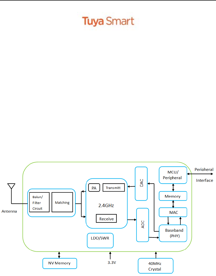
WR1 is a low power consumption module with built-in Wi-Fi connectivity solution designed
by Hangzhou Tuya Information Technology Co., Ltd. The Wi-Fi Module consists of a highly
integrated wireless radio chip W302 12E75M2 and some extra flash that has been programed
with Wi-Fi network protocol and plenty of software examples.WR1 include a ARM CM4F,
WLAN MAC, 1T1R WLAN, maximum frequency reaches 125MHz, 256K SRAM, 1M byte
flash and various peripheral resources.
WR1 is a RTOS platform, embedded with all the Wi-Fi MAC and TCP/IP protocol function
examples, users can customize their Wi-Fi product by using these software examples.
Figure 1 shows the block diagram of the WR1.
Figure 1. The block diagram of the WR1
1.1 Features
Integrated low power consumption 32-bit CPU, also known as application processor
Basic frequency of the CPU can support 125 MHz
Supply voltage range: 3V to 3.6V
Peripherals: 6 GPIO channels, 2 UART, 1 ADC
Wi-Fi connectivity:
802.11 B/G/N20/N40
Channel 1 to 11 @ 2.4GHz
Support WPA/WPA2
+21.10dBm output power in 802.11b mode

WR1DATASHEET
Support SmartConfig function for both Android and IOS devices
On-board PCB antenna
Operating temperature range: -20℃ to 105℃
1.2 Main Application Fields
Intelligent Building
Intelligent home, Intelligent household applications
Healthy devices
Industrial wireless control
Baby monitor
Webcam
Intelligent bus
WR1DATASHEET
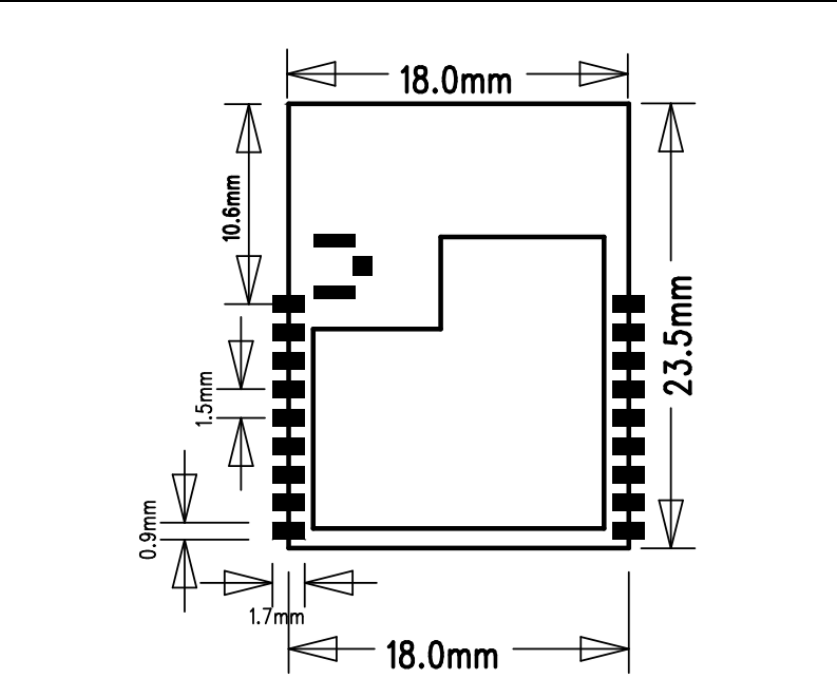
2. Dimensions and Footprint
2.1Dimensions
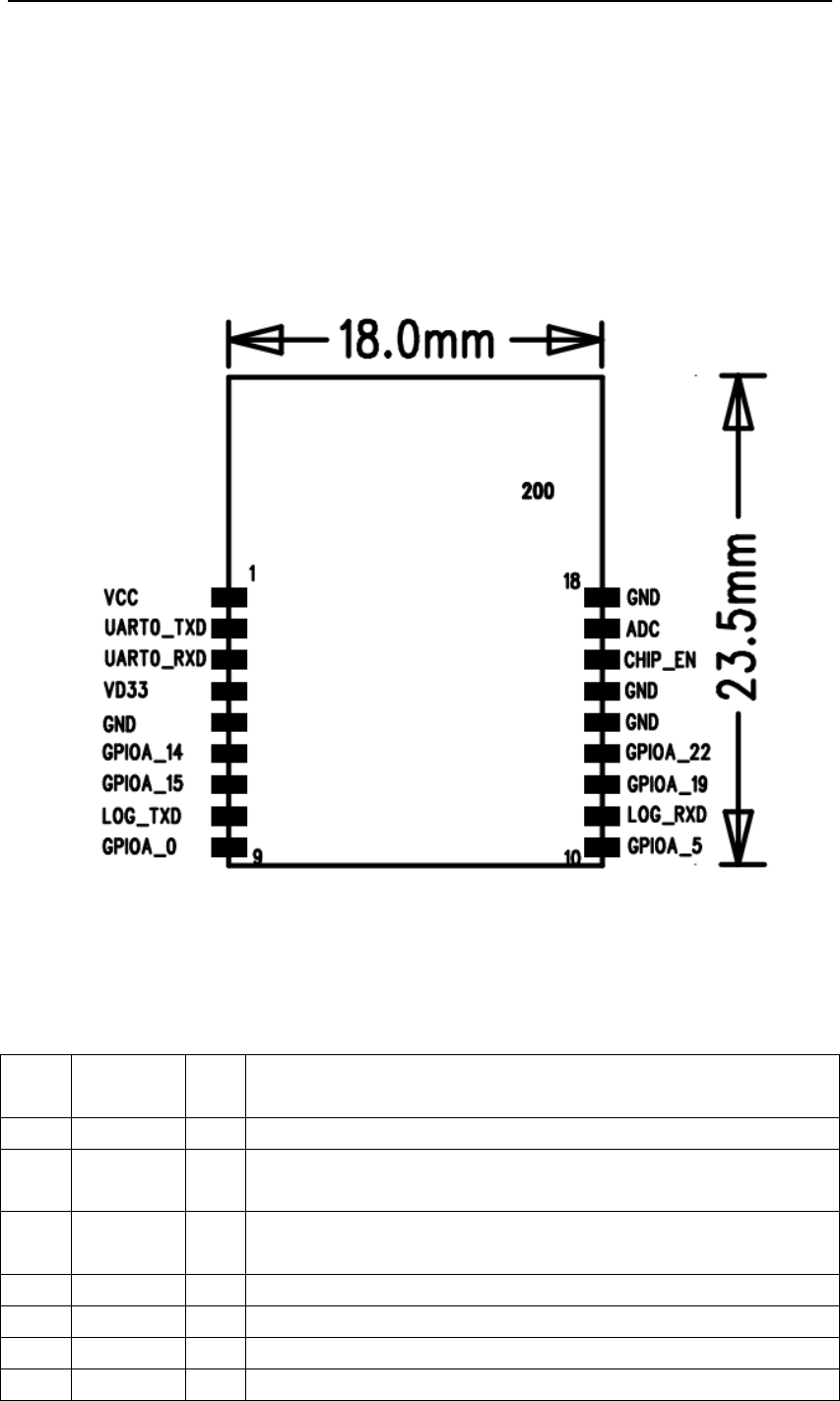
WR1 has 2 columns of Pins (2*9).The distance between each Pin is 1.5 mm.
Size of WR1: 18mm(W)*23.5mm(L)*3.1mm(H)
Figure 2 shows the dimensions of WR1.
Figure 2. The dimensions of WR1
2.2 Pin Definition
Table 1 shows the generalpin attributes of WR1
Table 1. The typical pin definition of WR1
PIN
NO.
NAMETYP
E
DISCREPTION
1VCCPSupplyvoltage(3.3V)
2UART0_TX
D
I/OUART0_TXD
3UART0_RX
D
I/OUART0_RXD
4VD33PSupplyvoltage(3.3V)
5GNDPGround
6GPIOA_14I/OGPIOA_14
7GPIOA_15I/OGPIOA_15

WR1DATASHEET
8LOG_TXDI/OUART_Log_TXD(usedtoprintmodule'sinternalinformation)
9GPIOA_0I/OGPIOA_0,cannotbepull‐upwhilebooting,canbeusedasGPIO
whileinnormalworkingmode
10GPIOA_5I/OGPIOA_5
11LOG_RXDI/OUART_Log_RXD(usedtoprintmodule'sinternalinformation)
12GPIOA_19I/OGPIOA_19
13GPIOA_22I/OGPIOA_22
14GNDPGround
15GNDPGround
16CHIP_ENI/OExternalresetsingal(lowleveleffects)
17ADCAIADCterminal(input5Vmaximally)
18GNDPGround
Note: S: Power supply pins; I/O: Digital input or output pins; AI: Analog input.

WR1DATASHEET
3. Electrical Characteristics
3.1 Absolute Maximum Ratings
Table 3.1. Absolute Maximum Ratings
PARA MET ERSDESCRIPTIONMINMAXUNIT
TsStoragetemperature‐20105℃
VCCSupplyvoltage ‐0.33.6V
Staticelectricityvoltage
(humanmodel)
TAMB‐25℃‐ 2KV
Staticelectricityvoltage
(machinemodel)
TAMB‐25℃‐ 0.5KV
3.2 Electrical Conditions
Table 3.2. Electrical Conditions
PARA MET ERSDESCRIPTIONMINTYPICAL MAXUNIT
TaWorkingtemperature ‐20‐ 105℃
VCCWorkingvoltage3‐3.6V
VILIOlowlevelinput ‐0.3‐ VCC*0.25V
VIHIOhighlevelinputVCC*0.75 ‐ VCCV
VOLIOlowleveloutput ‐‐VCC*0.1V
VoHIOhighleveloutputVCC*0.8‐ VCCV
ImaxIOdrivecurrent ‐‐16mA
CpadInputcapacitor ‐2‐pF
3.3 Wi-Fi Transmitting Current Consumptions
Table 3.3. Wi-Fi TX current consumption
PARAMETERSMODERATETransmittingpowerTYPICALUNIT
IRF11b1Mbps+21.10dBm287mA
IRF11g6Mbps+19.97dBm255mA
IRF MCS0 +20.09dBm244mA
IRF MCS0+20.19dBm220mA
n-HT20
11
11n-HT40

WR1DATASHEET
3.4 Wi-Fi Receiving Current Consumptions
Table 3.4. Wi-Fi RX currentconsumption
PARA MET ERSMODETYPICALUNIT
IRFCPUsleep90mA
IRFCPUactive120mA
3.5 Working Mode Current Consumptions
Table 3.5. The module working currentcon sumption
WORKMODEATTA= 2 5 ℃TYPICALMAX*UNIT
EZModeWR1isunderEZparingmode,Wi‐Fiindicator
lightflashesquickly
121.8141mA
StandbyModeWR1isconnected,Wi‐Fiindicatorlightison52125mA
OperationModeWR1isconnected,Wi‐Fiindicatorlightison180312mA
Disconnection
Mode
WR1isdisconnected,Wi‐Fiindicatorlightisoff 46120mA
Note: peak continuous time is about 5us.
The parameter shown above will vary dependingon different firmware functions.
4. WLAN Radio Specification
4.1 Basic Radio Frequency Characteristics
Table 41.Basic Radio frequency characteristics
PARA MET ERSDESCRIPTION
Frequencyband2412MHz-2462MHz
Wi‐FistandardIEEE802.11n20/n40/g/b(Terminal1‐11)
Datatransmittingrate11b:1,2,5.5,11(Mbps)
11g:6,9,12,18,24,36,48,54(Mbps)
11n:HT20,MCS0~7
11n:HT40,MCS0~7
AntennatypeOn‐boardPCBAntenna
4.2Wi-Fi Transmitting Power
Table 4.2. Wi-Fi transmitting power

WR1DATASHEET
PARA MET ERSMIN TYPICALMAXUNI
T
RFaverageoutputpower,802.11bCCKMode1M ‐21.10‐dBm
RFaverageoutputpower,802.11gOFDMMode6M ‐19.97‐dBm
RFaverageoutputpower,802.11n20OFDMMode MCS0‐ 20.09‐dBm
RFaverageoutputpower,802.11n40OFDMMode MCS0‐ 20.19‐dBm
TheFrequencyerror ‐10‐ 10ppm
4.3Wi-Fi Receiving Sensitivity
Table 4.3. Wi-Fi Receiving sensitivity
PARA MET ERSMIN TYPICALMAXUNI
T
PER<8%,Receivingsensitivity,802.11bCCKMode1M ‐ ‐91‐dBm
PER<10%,Receivingsensitivity,802.11gOFDMMode 6M ‐ ‐75‐dBm
PER<10%,Receivingsensitivity,802.11nOFDMMode MCS0 ‐ ‐72‐dBm
WR1DATASHEET
5. Antenna Information
5.1 Antenna Type
Antenna can be connectedusing On-board PCB antenna
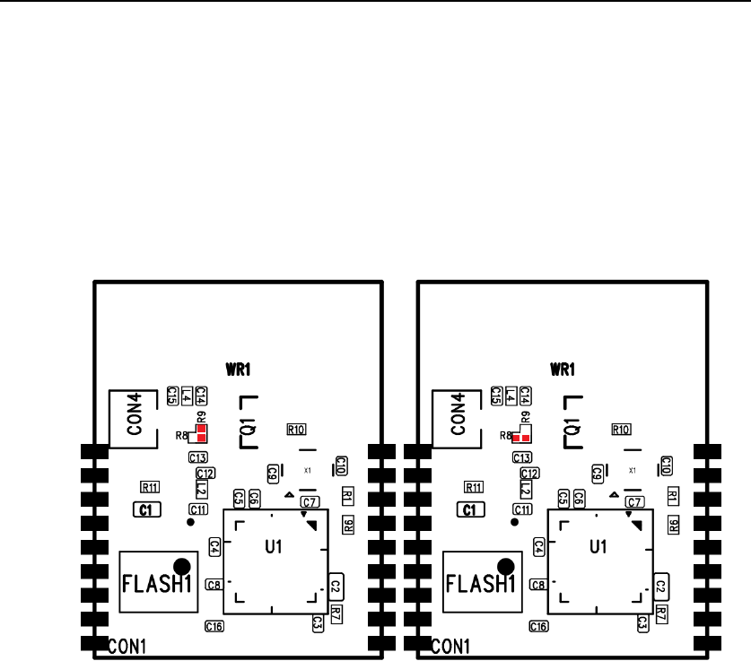
Figure 5.1. Resistor definition for on-board PCB antenna Figure 5.2. Resistor definition for external antenna
5.2 Antenna Interference
While using the On-board PCBantenna, in order to have the best Wi-Fi performance, it’s
recommended to keep a minimum15mm distance between the antenna part and the other metal
pieces.
User’s own PCBA design is recommended NOT to pass any wire, NOT do copper pour under
the region of the module’s antenna, to avoid interferences.
WR1DATASHEET
6. Packaging Information And Production Guide
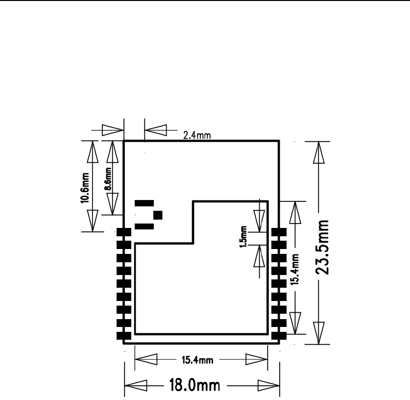
6.1 Mechanical Dimensions
Figure 6.1. Top view of the module
6.2PCB Recommended Package
WR1DATASHEET
6.3 Production Guide
The storage for the delivered module should meet the following condition:
1. The anti-moisture bag should be kept in the environment withtemperature< 30℃ and
humidity< 85% RH.
2. The expiration date is 6 months since the dry packaging products was sealed.
Cautions:
1. All the operators should wear electrostatic ringin the whole process of production.
2. While operating, water and dirt should not have any contact with the modules.
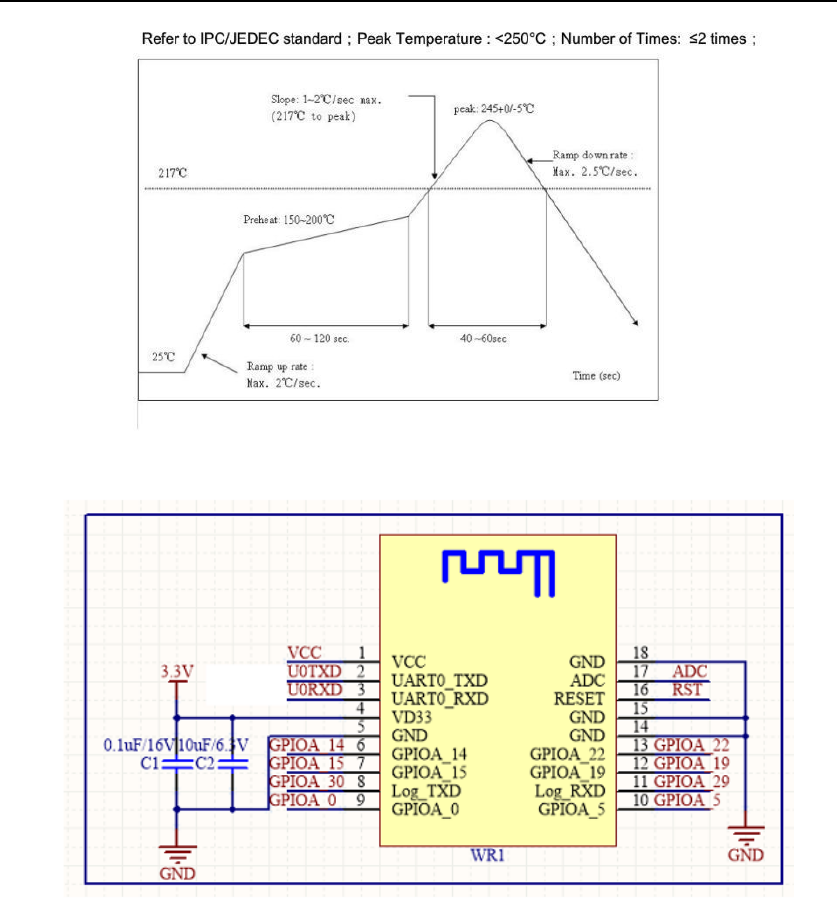
6.4 Recommended furnace temperature curve
Figure 6.4. PCB Package DrawingRecommended furnace temperature curve
WR1DATASHEET
Figure A.1. The application schematic design of the module
FCC Statement
Any Changes or modifications not expressly approved by the party responsible for compliance
could void the user’s authority to operate the equipment.
This device complies with part 15 of the FCC Rules. Operation is subject to the following two
conditions:
(1) This device may not cause harmful interference, and
(2) This device must accept any interference received, including interference that may cause
undesired operation.
FCC Radiation Exposure Statement:
This equipment complies with FCC radiation exposure limits set forth for an
uncontrolled environment .This equipment should be installed and operated with
minimum distance 20cm between the radiator& your body.
FCC Label Instructions:
The outside of final products that contains this module device must display a label
referring to the enclosed module. This exterior label can use wording such as: “Contains
Transmitter Module FCC ID:2ANDL-WR1”,or “Contains FCC ID:2ANDL-WR1”, Any similar
wording that expresses the same meaning may be used.