Hansong DECT Wireless Module User Manual XCO DECT 1
Hansong(Nanjing) Technology Ltd. Wireless Module XCO DECT 1
UserManual.wiki
>
Hansong
>
DECT User Manual
XCO-DECT_User Manual_1
Navigation menu
Upload a User Manual
Namespaces
Wiki Guide
HTML
PDF
Info
Views
User Manual
Discussion / Help
Navigation
![HANSONG 1 Terms and definitions BoM CODEC GPIO GND HDI I2C I2S JTAG LED Lx PCB RF SMD UART USB Bill of Materials COder / DECoder General Purpose Input / Output (pin) Ground High Density Interconnect Inter-IC (serial communication interface) Inter-IC sound; in the context of this document it is in relation to the interface on the module that is the scope in this document Joint Test Action Group (specification of debug interface) Light Emitting Diode Layer x Printed Circuit Board Radio Frequency Surface Mount Device Universal Asynchronous Receiver / Transmitter Universal Serial Bus digital audio 2 References [1] Dialog SmartBeat Wireless Audio brochure [2] SC14492_493, Datasheet: “Single Chip ZBS DECT Audio Transceiver with USB”, Dialog Semiconductor User manual Revision 1.0 12-13-2017 3 of 18 © 2017 Hansong](https://usermanual.wiki/Hansong/DECT/User-Guide-3933761-Page-3.png)
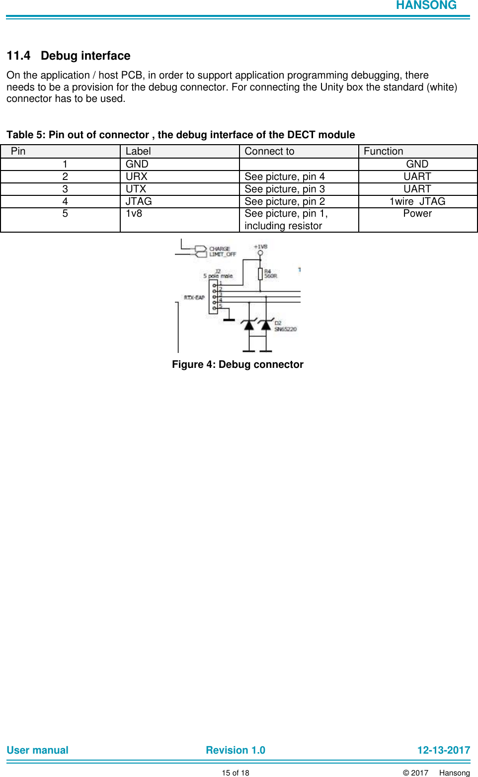
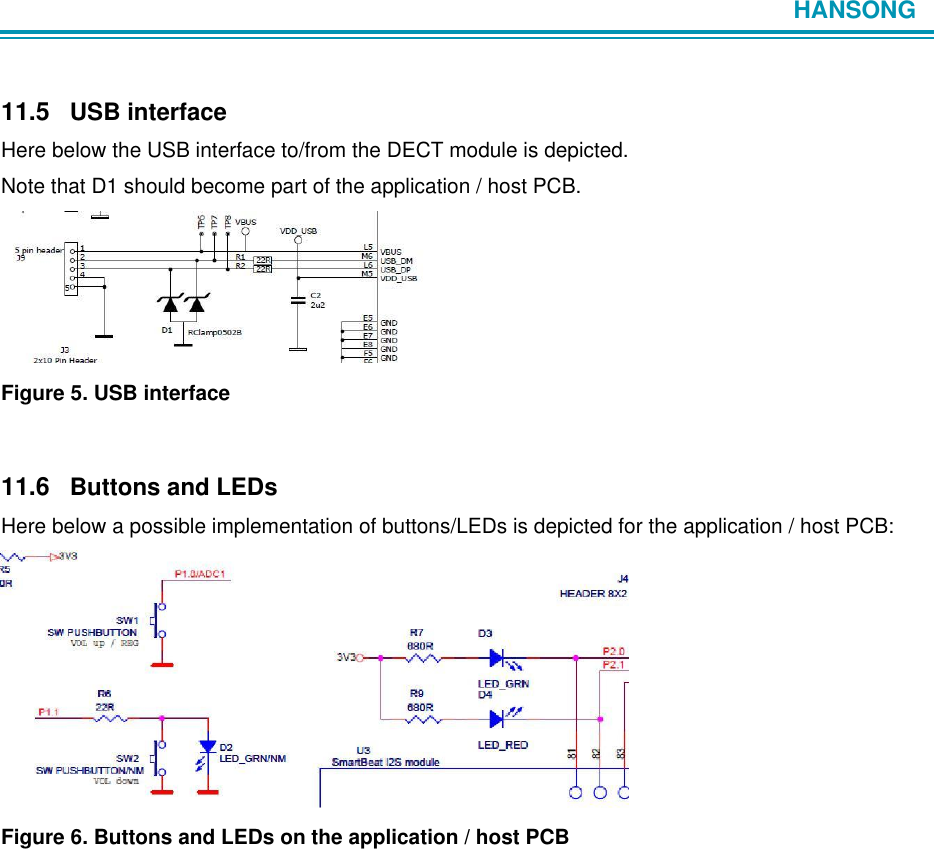
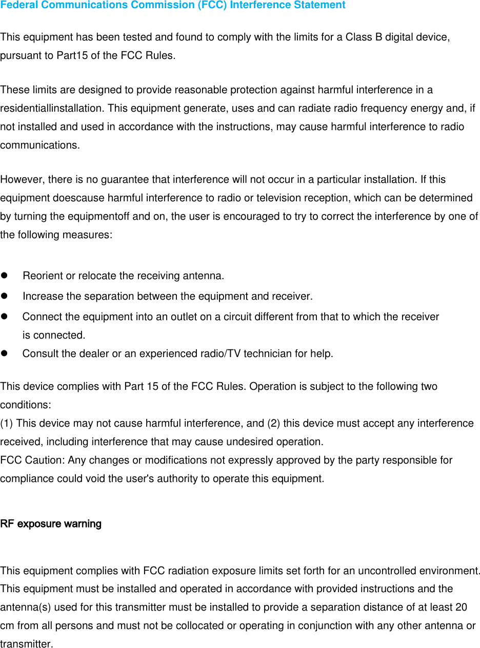
![HANSONG Name/ Description Power Power supply input pin of I2S module. GND Connect to application PCB GND plane JTAG JTAG debug pin of SC14492 (pin A10) UART_TX UART TX, P0[0] of SC14492, connect to application PCB UART RX pin if UART support is required UART_RX UART RX, P0[1] of SC14492, connect to application PCB UART TX pin if UART support is required LED 1/2 Can be used to drive external LED 1/2 GPIO1/2/3 GPIO pin used to connect to external switch, LED or other digital IO device I2C_SDA I2C interface serial data pin, P0[2] of SC14492; requires external pull up resistor I2C_SCL I2C interface serial clock pin, P0[3] of SC14492; requires external pull up resistor I2S data in I2S interface data input of SC14492 on I2S module (connect to external audio ADC/DAC I2S output) I2S data out I2S interface data output of SC14492 on I2S module (connect to external audio ADC/DAC I2S input) BCLK I2S interface bit clock LRCK I2S interface left/right clock USB _DM USB interface data ”-” USB_DP USB interface data ”+” RF ANT 1/2 RF antenna 1/2: printed antenna with optional U.FL/IPEX connector for external antenna support VBUS USB supply voltage (input to module) 1V8 1V8 power supply output of I2S module that can be used to supply e.g. external audio ADC/DAC Optional I2S master clock output: note that this is a BXTAL 10.368MHz signal. In case e.g. 12.288MHz is required, an external PLL may be required. Reset Active low reset signal to reset SC14492 of I2S module Note that the digital IO levels (except I2C) are 1.8V. Please also refer to the SC14492 datasheet [2] for further pinning details. User manual Revision 1.0 12-13-2017 9 of 18 © 2017 Hansong](https://usermanual.wiki/Hansong/DECT/User-Guide-3933761-Page-10.png)