Hansong DECT Wireless Module User Manual XCO DECT 1
Hansong(Nanjing) Technology Ltd. Wireless Module XCO DECT 1
Hansong >
XCO-DECT_User Manual_1
User manual
DECT Module
User Manual
Abstract
This document provides user guide lines for the DECT Module reference design:
HW description, schematic and PCB details, testability.

HANSONG
Contents
Abstract ................................................................................................................................................
1
Contents ...............................................................................................................................................
2
Figures ..................................................................................................................................................
2
Tables ...................................................................................................................................................
2
1
Terms and definitions ...................................................................................................................
3
2
References .....................................................................................................................................
3
3
Introduction....................................................................................................................................
4
4
General description, block diagram ............................................................................................
5
5
Specifications ................................................................................................................................
6
6
Schematics.....................................................................................................................................
7
7
Interface Pinning ...........................................................................................................................
8
8
Layout ...........................................................................................................................................
10
9
BoM ...............................................................................................................................................
11
10
PCB Stackup ................................................................................................................................
12
11
Application PCB guidelines .......................................................................................................
13
11.1
RF considerations ...............................................................................................................
13
11.2
Routing ................................................................................................................................
13
11.3
Testability ............................................................................................................................
14
11.4
Debug interface ...................................................................................................................
15
11.5
USB interface ......................................................................................................................
16
11.6
Buttons and LEDs ...............................................................................................................
16
Revision history .................................................................................................................................
17
Figures
Figure 1: Block diagram of DECT Module ............................................................................................. 5
Figure 2: DECT Module Schematics ..................................................................................................... 7
Figure 3: Layout plot of DECT Module ................................................................................................ 10
Figure 4: Debug connector .................................................................................................................. 15
Figure 5. USB interface ....................................................................................................................... 16
Figure 6. Buttons and LEDs on the application / host PCB ................................................................ 16
Tables
Table 1: Specifications table ................................................................................................................. 6
Table 2: Interface connector pinning ..................................................................................................... 8
Table 3: Bill of Materials List ............................................................................................................... 11
Table 4: PCB Layer Stackup ............................................................................................................... 12
Table 2: Pin out of connector , the debug interface of the DECT module........................................... 15
User manual
Revision 1.0
12-13-2017
2 of 18
© 2017 Hansong

HANSONG
1 Terms and definitions
BoM
CODEC
GPIO
GND
HDI
I2C
I2S
JTAG
LED
Lx
PCB
RF
SMD
UART
USB
Bill of Materials
COder / DECoder
General Purpose Input / Output (pin)
Ground
High Density Interconnect
Inter-IC (serial communication interface)
Inter-IC sound; in the context of this document it is in relation to the
interface on the module that is the scope in this document
Joint Test Action Group (specification of debug interface)
Light Emitting Diode
Layer x
Printed Circuit Board
Radio Frequency
Surface Mount Device
Universal Asynchronous Receiver / Transmitter
Universal Serial Bus
digital audio
2 References
[1] Dialog SmartBeat Wireless Audio brochure
[2] SC14492_493, Datasheet: “Single Chip ZBS DECT Audio Transceiver with USB”, Dialog
Semiconductor
User manual
Revision 1.0
12-13-2017
3 of 18
© 2017 Hansong

HANSONG
3 Introduction
This document aims to serve as a guide line in regard to the DECT Module and its use on
application level.
The DECT Module is an example HW implementation of the SC14492 chip on a module, to support
the development of wireless speaker systems. The air interface is based on the DECT standard,
meaning that the system can coexist with regular DECT systems such as DECT phones.
The audio CODEC that is used for audio compression is CELT (sample rate: 48kHz).
The DECT Module is meant to serve as a reference design only. The design files can be made
available upon request.
User manual
Revision 1.0
12-13-2017
4 of 18
© 2017 Hansong
HANSONG
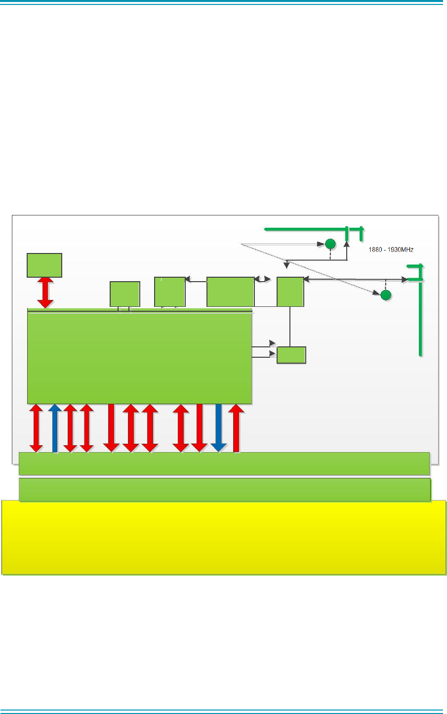
4 General description, block diagram
The DECT Module is a reference design for a SC14492-based module/product. It is a self-
contained unit, including the required supporting components such as crystal, FLASH, DC supply
and RF circuitry.
The module enables a platform-based product development, in which the RF development is
leveraged over multiple products. To further support this platform-based approach, the module
is suited to run the Hansong firmware that is fully configurable and enables easy customization
without requiring full SW development.
The module supports all required standard interfacing, such as I2S, I2C, USB and GPIO.
The following figure shows the basic module’s block diagram and its interfacing to the application
PCB:
IPEX Connector
QSPI
Flash
RX
RX/TX
Ant
Con
trol
XTAL
(20.736
MHz)
balun
Switch
Switch
TX
Sc14492
balun
DP/DM
DC_IN and
VBUS
I2C
I2S/PCM
BXTAL
UART
JTAG
GPIO
LED
1V8
Reset
MAIN MODULE
Board interconnect
Board interconnect
Add-on board
Figure 1: Block diagram of DECT Module
User manual
Revision 1.0
12-13-2017
5 of 18
© 2017 Hansong
HANSONG
5
Specifications
Table 1: Specifications table
Parameter
Value
Note
Module size
40.8mm x 36.5mm x 1.6mm
Fully embedded module,
including RF, FLASH, crystal
Mating connector
R6850-36TR-SMT
Or equivalent
Operating temperature range
0…+50C
Ambient
Interfacing
I2S (input and output)
FP = I2S Slave, PP = I2S
I2C
Master
USB
JTAG
UART
GPIOs
For LEDs and buttons
Antennas
2 printed PIFA
Optional up to 2 external
Antenna diversity support
antennas (U.FL Hirose / IPEX)
Antenna radiation pattern
Dipole, 2dBi
Operating frequency range
1880 - 1930MHz
EU DECT, US DECT
Current consumption
160 / 95 mA
FP / PP
Input power supply voltage
3.6V~5.0V
±150 mV
GPIO I/O levels
1.8 V
Type approval
ETSI/FCC
Pre-test only. Full certification
will need to be performed by
the customer. Changes to the
reference design may invalidate
the pre-test results.l
Range
50 m indoor, 300 m outdoor
User manual
Revision 1.0
12-13-2017
6 of 18
© 2017 Hansong
HANSONG
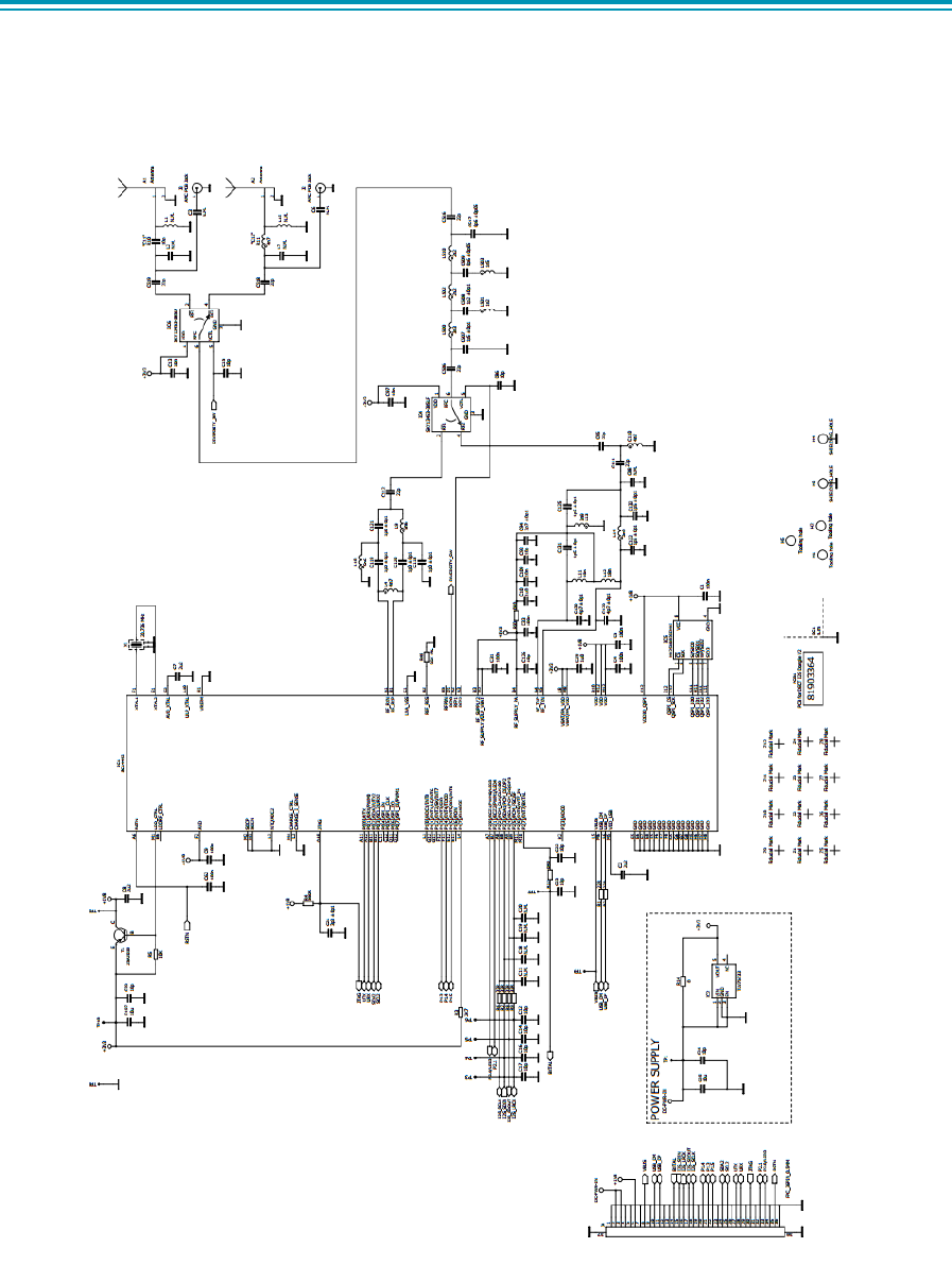
6 Schematics
Figure 2: DECT Module Schematics
User manual
Revision 1.0
12-13-2017
7 of 18 © 2017 Hansong
FCC Frequency
CE Frequency
HANSONG
7
Interface Pinning
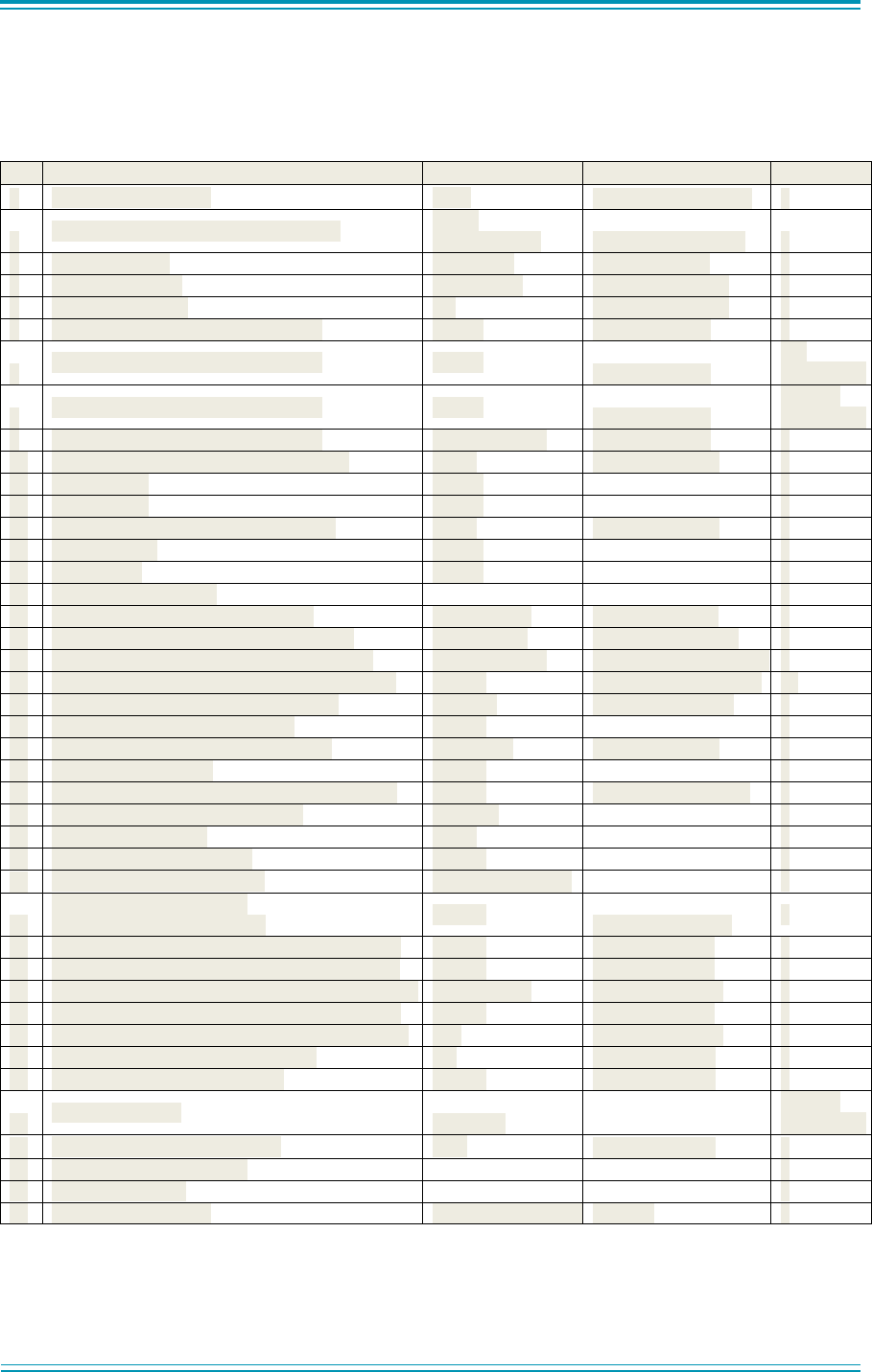
Table 2: Interface connector pinning
Connector pinning
Pin
Description
Pin
Description
1
GND
19
GND
2
DC-PWR-IN
20
GPIO_P1.4
3
DC-PWR-IN
21
GPIO_P1.3
4
GND
22
GPIO_P1.5
5
GND
23
GND
6
1V8
24
I2C_SDA2
7
GND
25
I2C_SCL2
8
VBUS
26
GND
9
GND
27
UART_TX
10
USB_DM
28
UART_RX
11
USB_DP
29
GND
12
GND
30
JTAG
13
GND
31
GND
14
BXTAL
32
GPIO_P2.1(LED)
15
I2S_SDIN
33
GPIO_P2.0(LED)
16
I2S_LRCK
34
GND
17
I2S_SDOUT
35
RSTN
18
I2S_SCLK
36
GND
The interface connector pins are also available on test pins (see also section 11.3).
Next to the connector pinning described here above, the DECT Module also holds two RF connectors that can be
used to connect one or two external antenna(s). These are standard U.FL Hirose (IPEX) connectors.
Note that using these will require changing some components on the PCB. Please contact Hansong
support for further details.
User manual
Revision 1.0
12-13-2017
8 of 18
© 2017 Hansong
HANSONG
Name/
Description
Power
Power supply input pin of I2S module.
GND
Connect to application PCB GND plane
JTAG
JTAG debug pin of SC14492 (pin A10)
UART_TX
UART TX, P0[0] of SC14492, connect to application PCB
UART RX pin if UART support is required
UART_RX
UART RX, P0[1] of SC14492, connect to application PCB
UART TX pin if UART support is required
LED 1/2
Can be used to drive external LED 1/2
GPIO1/2/3
GPIO pin used to connect to external switch, LED or other
digital IO device
I2C_SDA
I2C interface serial data pin, P0[2] of SC14492; requires
external pull up resistor
I2C_SCL
I2C interface serial clock pin, P0[3] of SC14492; requires
external pull up resistor
I2S data in
I2S interface data input of SC14492 on I2S module (connect
to external audio ADC/DAC I2S output)
I2S data out
I2S interface data output of SC14492 on I2S module
(connect to external audio ADC/DAC I2S input)
BCLK
I2S interface bit clock
LRCK
I2S interface left/right clock
USB _DM
USB interface data ”-”
USB_DP
USB interface data ”+”
RF ANT 1/2
RF antenna 1/2: printed antenna with optional U.FL/IPEX
connector for external antenna support
VBUS
USB supply voltage (input to module)
1V8
1V8 power supply output of I2S module that can be used to
supply e.g. external audio ADC/DAC
Optional I2S master clock output:
note that this is a
BXTAL
10.368MHz signal. In case e.g. 12.288MHz is required, an
external PLL may be required.
Reset
Active low reset signal to reset SC14492 of I2S module
Note that the digital IO levels (except I2C) are 1.8V.
Please also refer to the SC14492 datasheet [2] for further pinning details.
User manual
Revision 1.0
12-13-2017
9 of 18
© 2017 Hansong
HANSONG
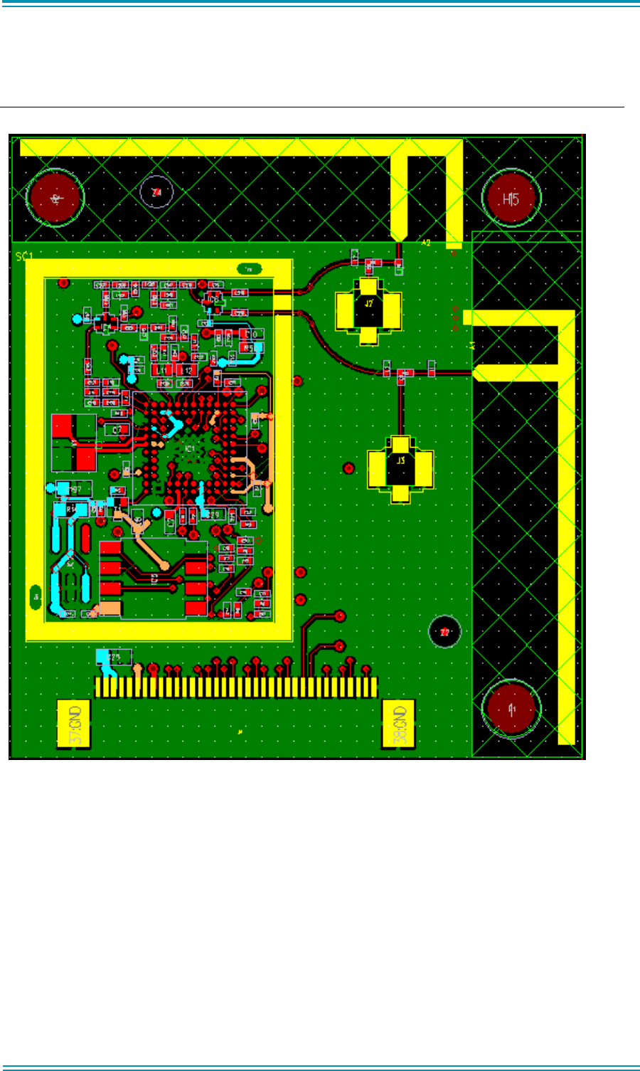
8 Layout
Here below a layout plot is depicted of the DECT Module:
Figure 3: Layout plot of DECT Module
User manual
Revision 1.0
12-13-2017
10 of 18
© 2017 Hansong
HANSONG
9
BoM
Table 3: Bill of Materials List
ID
Description
Manufacturer
Order number
Count
1
MX25U8035EM1I-10G
MXIC
MX25U8035EM1I-10G
1
2
SC14492,ZBS DECT Transceiver with USB
Dialog
Semiconductor
SC14492A76R101ULC
1
3
SKY13453-385LF
SKYWORKS
SKY13453-385LF
2
4
AP2112K-3.3TRG1
Diodes(BCD)
MMBT4403M3T5G
1
5
MMBT4403M3T5G
ON
MMBT4403M3T5G
1
6
0Ω,0201,1/20W,±5%,RC0201JR-070RL
YAGEO
RC0201JR-070RL
1
7
0Ω,0201,1/20W,±5%,RC0201JR-070RL
YAGEO
RC0201JR-070RL
pcb
antenna:2
8
0Ω,0201,1/20W,±5%,RC0201JR-070RL
YAGEO
RC0201JR-070RL
external
antenna:2
9
0Ω,0402,1/16W,±5%,RC0402JR-070RL
Yageo/Phicomp
RC0402JR-070RL
1
10
10KΩ,0201,1/20W,±5%,RC0201JR-0710KL
Yageo
RC0201JR-0710KL
1
11
22R±5%,0201
YAGEO
2
12
2K7±5%,0201
YAGEO
1
13
33Ω,0201,1/20W,5%, RC0201JR-0733RL
Yageo
RC0201JR-0733RL
4
14
560R±5%,0201
YAGEO
1
15
56k 1% 0201
YAGEO
1
16
0.6p +/- 0.05 NP0,0201
2
17
1uK,16V,0402,X5R,C1005X5R1C105K
TDK/Phicomp
C1005X5R1C105K
2
18
100nF,10V,±10%,X5R,C0201KRX5R6BB104
TDK / YAGEO
C0201KRX5R6BB104
7
19
10nK,10V,0201,X7R,C0603X7R1A103KT00NN
Yageo/Phicomp
C0603X7R1A103KT00NN
3
20
10pF 25V ±5% 0201NPO,GRM0335C1E100JD01D
Murata
GRM0335C1E100JD01D
12
21
10uK,10V,0603,X5R,CL10A106KP8NNNC
Samsung
CL10A106KP8NNNC
1
22
CAP,0201,C0G,1.0pF,+/-0.1pF,25V
Murata
4
23
1.2pC,25V,0201,NPO,C0603C0G1E1R2C
TDK/Yageo
C0603C0G1E1R2C
1
24
1p5 ,+/-0.1pF NP0 25V
Murata
5
25
22pF 50V ±5% 0201 NPO, CC0201JRNPO9BN220
Murata
CC0201JRNPO9BN220
7
26
CAP,0201,C0G,2.7pF,+/-0.25pF,25V
MURATA
1
27
2.2uM,6.3V,0402,X5R
Yageo
3
28
3p3 ,+/-0.1pF NP0 25V,0201
Murata
1
29
4.7pF,+/-0.1pF,25V,0201,NPO
TDK/Yageo/和伸堂
2
30
Coil, chip 18nH Wirewound
±3%,LQW15AN18NH00x,0402
Murata
LQW15AN18NH00x
2
31
Inductor Chip 1n2,±0.1nH,LQP03TN1N2B02,0201
Murata
LQP03TN1N2B02
1
32
Inductor Chip 1n5'±0.1nH,LQP03TN1N5B02,0201
Murata
LQP03TN1N5B02
1
33
HK0603 2N2S-T,2.2 ±0.3nH,LQP03TN2N2B02#,0201
TAIYO YUDEN
LQP03TN2N2B02#
2
34
Inductor Chip 3n3,±0.1nH,LQP03TN3N3B02,0201
Murata
LQP03TN3N3B02
1
35
Inductor Chip 3n9'±0.1nH,LQP03TN3N9B02#,0201
TDK
LQP03TN3N9B02#
2
36
4.7nH ±0.3nH,LQP03TN4N7H02,0201
WE
LQP03TN4N7H02
2
37
5n6 '±3%,LQP03TN5N6H02,0201
Murata
LQP03TN5N6H02
2
38
KFM110Z-1002-7F
FOXCONN
external
antenna:2
39
36PIN,0.5mm, R6850-36TR-SMT
晋宇
R6850-36TR-SMT
1
40
SHIELDING COVER FRAM-2
1
41
SHIELDING COVER
1
42
TZ1284B, 20.736 MHz
TAI-SAW Technology
TZ1284B
1
User manual
Revision 1.0
12-13-2017
11 of 18
© 2017 Hansong
HANSONG
10 PCB Stackup
Table 4: PCB Layer Stackup
Parameter
Value
Note
Board Definition
PCB
Rigid
Stack-up
1-2-1
SMD
Single-sided
Via-type
Through, microvia
Layer Definition
Multilayer – 4L
Laminate
FR-4
Board size
36.5mm x 40.0mm
+/-0.2mm
Board thickness
1.6mm
+/-10%
Surface finish
Immersion Gold
User manual
Revision 1.0
12-13-2017
12 of 18
© 2017 Hansong

HANSONG
11 Application PCB guidelines
This section describes some guidelines in relation to the use of the DECT Module with the
application (host) PCB.
11.1 RF considerations
To ensure optimum wireless performance of the DECT Module, special attention should be paid to
the antenna selection and placement. In case the internal/embedded printed antennas are used,
the module location would be best selected by focusing on the following:
● Ensure that the antennas are uninhibited as much as possible (e.g. by placing the module at
the corner of the application PCB
● Ensure that no components , traces or ground/power planes are close to the module; they
should preferably be spaced >>2cm away
● The module location with respect to the product’s enclosure should be such that the antennas
are not close to conductive parts (e.g. metallic paint, metal parts, wiring, …)
○ Should this be insufficiently feasible, it can be considered to use external antennas instead,
to have optimum design freedom with respect to the antenna placement for optimum
performance
● The antennas may radiate significant RF power. Care should be taken to ensure that e.g. an
analog audio ADC/DAC is not affected by this (i.e. rectifying the RF energy inside the
ADC/DAC and causing audible artefacts). This can be accomplished by any of the following:
○ Ensure sufficient physical separation between the antennas
○ Use a C-R-C filtering pi-network at the analog audio IO (e.g. R=33Ohm, C=10pF)
● The module has a provision for an optional RF shield that can be used to minimize EMC/EMI
in case this is required on the application level
11.2 Routing
High speed signals, such as the I2S bus (most notably the BLCK) and/or other digital/clock
signals should be routed with great care, to ensure that their harmonics aren’t received by the
module’s antennas, limiting its receiver sensitivity. To this effect, the following can be considered:
● Use C-R-C filtering pi-networks on signal lines that are high speed
● Route high speed signals on inner layers, while ensuring that they are sandwiched
between power/GND planes for optimum shielding/isolation
Other general audio/RF design guidelines would apply, such as the use of a good (uninterrupted)
system ground plane, sufficiently thick traces for the power supply routing, etc.
Also, to minimize current switching noise from the module to the application PCB, it may
be advisable to use solid, wide frequency1 decoupling close to the connector.
1 E.g. at least a large valued capacitor, e.g. 100uF, to buffer the larger LF current peaks and 10pF to decouple the RF content.
User manual
Revision 1.0
12-13-2017
13 of 18
© 2017 Hansong

HANSONG
11.3 Testability
BAT files can be made available that configure the module in specific test modes that can be
used for production level testing.
The interface pins are also available on test pins, located on the bottom side of the PCB, suitable
for a bed-of-nails (pogo-pins) test bed (pin-to-pin spacing >100 mil).
User manual
Revision 1.0
12-13-2017
14 of 18
© 2017 Hansong
HANSONG
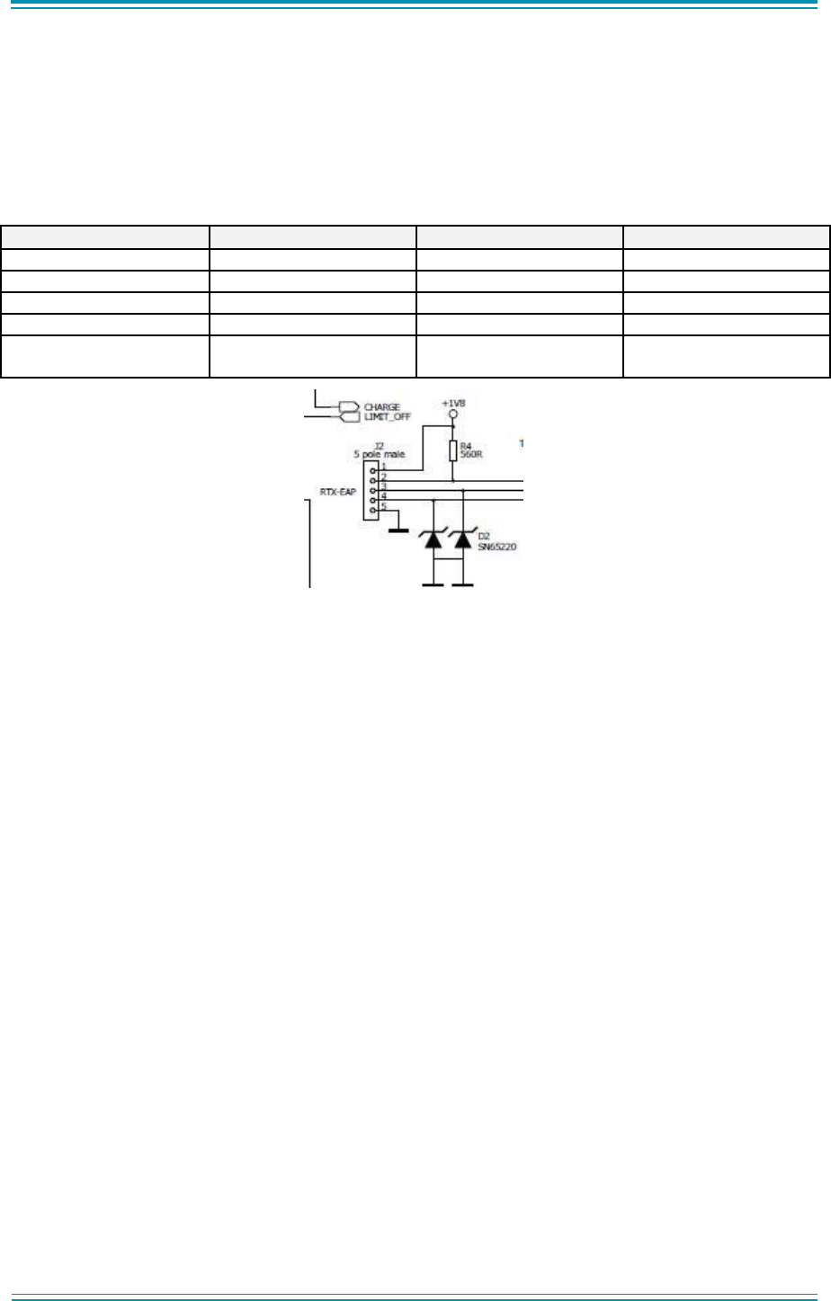
11.4 Debug interface
On the application / host PCB, in order to support application programming debugging, there
needs to be a provision for the debug connector. For connecting the Unity box the standard (white)
connector has to be used.
Table 5: Pin out of connector , the debug interface of the DECT module
Pin
Label
Connect to
Function
1
GND
GND
2
URX
See picture, pin 4
UART
3
UTX
See picture, pin 3
UART
4
JTAG
See picture, pin 2
1wire JTAG
5
1v8
See picture, pin 1,
Power
including resistor
Figure 4: Debug connector
User manual
Revision 1.0
12-13-2017
15 of 18
© 2017 Hansong
HANSONG
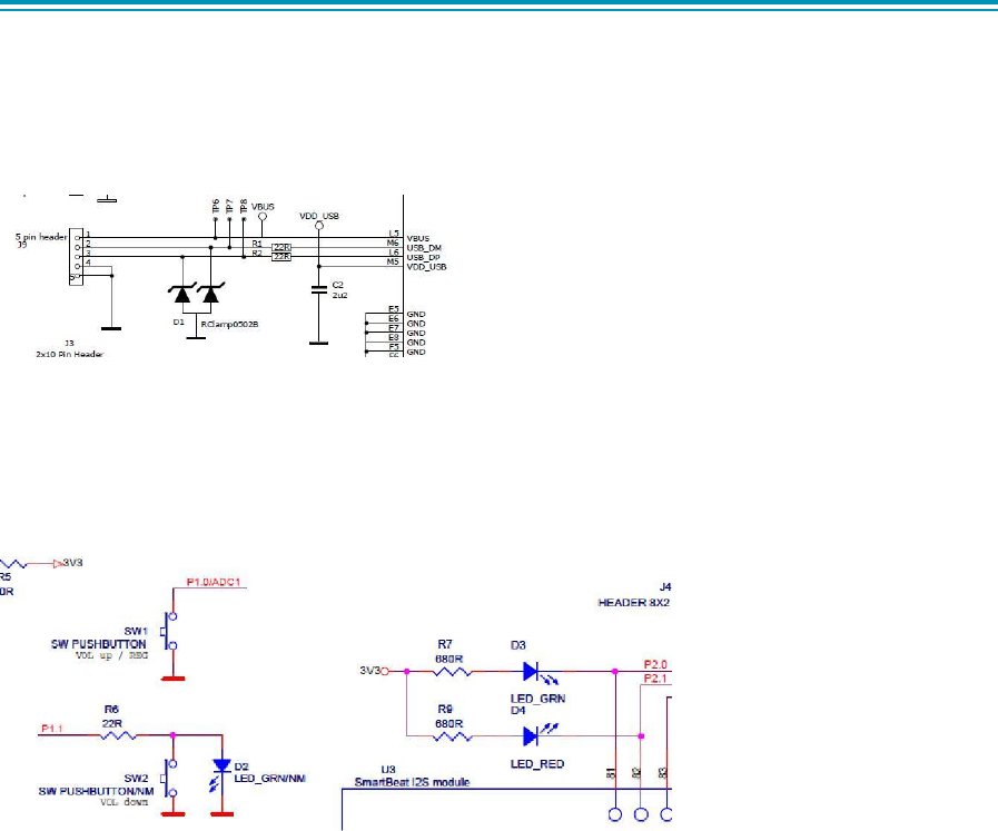
11.5 USB interface
Here below the USB interface to/from the DECT module is depicted.
Note that D1 should become part of the application / host PCB.
Figure 5. USB interface
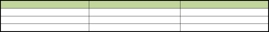
11.6 Buttons and LEDs
Here below a possible implementation of buttons/LEDs is depicted for the application / host PCB:
Figure 6. Buttons and LEDs on the application / host PCB

Federal Communications Commission (FCC) Interference Statement
This equipment has been tested and found to comply with the limits for a Class B digital device,
pursuant to Part15 of the FCC Rules.
These limits are designed to provide reasonable protection against harmful interference in a
residentiallinstallation. This equipment generate, uses and can radiate radio frequency energy and, if
not installed and used in accordance with the instructions, may cause harmful interference to radio
communications.
However, there is no guarantee that interference will not occur in a particular installation. If this
equipment doescause harmful interference to radio or television reception, which can be determined
by turning the equipmentoff and on, the user is encouraged to try to correct the interference by one of
the following measures:
Reorient or relocate the receiving antenna.
Increase the separation between the equipment and receiver.
Connect the equipment into an outlet on a circuit different from that to which the receiver
is connected.
Consult the dealer or an experienced radio/TV technician for help.
This device complies with Part 15 of the FCC Rules. Operation is subject to the following two
conditions:
(1) This device may not cause harmful interference, and (2) this device must accept any interference
received, including interference that may cause undesired operation.
FCC Caution: Any changes or modifications not expressly approved by the party responsible for
compliance could void the user's authority to operate this equipment.
RF exposure warning
This equipment complies with FCC radiation exposure limits set forth for an uncontrolled environment.
This equipment must be installed and operated in accordance with provided instructions and the
antenna(s) used for this transmitter must be installed to provide a separation distance of at least 20
cm from all persons and must not be collocated or operating in conjunction with any other antenna or
transmitter.
Industry Canada (IC)
CAN ICES-3 (B)/NMB-3(B)
This device complies with Industry Canada’s licence-exempt RSSs. Operation is subject to the
following two conditions:
(1) This device may not cause harmful interference, and
(2) this device must accept any interference received, including interference that may cause
undesired operation.
Cetappareilestconforme à la norme RSS d'Industrie Canada. Son fonctionnementestsujet aux deux
conditions suivantes:
(1) ledispositif ne doit pas produire de brouillagepréjudiciable, et
(2) cedispositifdoit accepter tout brouillagereçu, y compris un brouillage susceptible de provoquer un
fonctionnementindésirable.
IMPORTANT NOTE:
Radiation Exposure Statement:
This equipment complies with IC radiation exposure limits set forth for an uncontrolled environment.
This equipment should be installed and operated with minimum distance 20cm between the radiator
and your body.
Déclarationd'exposition aux radiations:
Cetéquipementestconforme aux limitesd'exposition aux rayonnements IC établies pour
unenvironnement non contrôlé. Cetéquipementdoitêtreinstalléetutilisé avec un minimum de 20cm de
distance entre la source de rayonnement et votre corps.
OEM Integration Instructions:
This device is intended only for OEM integrators under the following conditions:
The module can be used to installation in other host. The antenna must be installed such that 20 cm
is maintained between the antenna and users, and the transmitter module may not be co-located with
any other transmit or antenna. The module shall be only used with the integral antenna(s) that has
been originally tested and certified with this module. As long as 3 conditions above are met, further
transmitter test will not be required. However, the OEM integrator is still responsible for testing their
end-product for any additional compliance requirement with this module installed (for example, digital
device emission, PC peripheral requirements, etc.)
IMPORTANT NOTE:
In the event that these conditions cannot be met (for example certain laptop configuration or co-
location with another transmitter), then the FCC authorization for this module in combination with the
host equipment is no longer considered valid and the FCC ID of the module cannot be used on the
final product. In these and circumstance, the OEM integrator will be responsible for re-evaluating. The
end product (including the transmitter) and obtaining a separate FCC authorization. The final end
product must be labeled in a visible area with the following: “Contains Transmitter Module FCC ID:
XCO-DECT or Contains FCC ID: XCO-DECT”.
Antenna Specification:
Antenna Type
Part No.
Peak Antenna Gain
Dipole Antenna
N/A
2dBi
Monopole Antenna
45-2-000272
2dBi
PCB Antenna
RC12WFI0283A1
2dBi
IMPORTANT NOTE:
This DECT Module (IC: 7756A-DECT) has been approved by Industry Canada to operate with the
antenna types listed below with the maximum permissible gain indicated. Antenna types not included
in this list, having a gain greater than the maximum gain indicated for that type, are strictly prohibited
for use with this device.
The Host Marketing Name(HMN) must be displayed (according to e-labelling requirements) or
indicated at any location on the exterior of the host product or product packaging or product literature,
which shall be available with the host product or online.
The host product shall be properly labelled to identify the modules within the host product. The
Innovation, Science and Economic Development Canada certification label of a module shall be
clearly visible at all times when installed in the host product; otherwise, the host product must be
labelled to display the Innovation, Science and Economic Development Canada certification number
for the module, preceded by the word “Contains” or similar wording expressing the same meaning, as
follows: Contains IC: 7756A-DECT.
Antenna Specification:
Antenna Type
Part No.
Peak Antenna Gain
Dipole Antenna
N/A
2dBi
Monopole Antenna
45-2-000272
2dBi
PCB Antenna
RC12WFI0283A1
2dBi
User manual
Revision 1.0
12-13-2017
16 of 18
© 2017 Hansong

Revision history
Revision
Date
Description
1.0
13-Dec-2017
Initial version.
User manual
Revision 1.0
12-13-2017
17 of 18
© 2017 Hansong