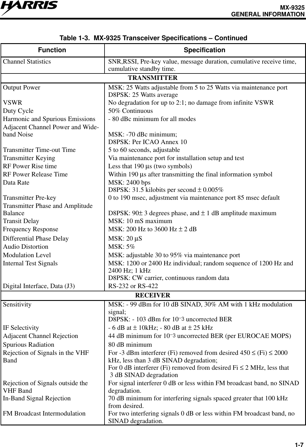
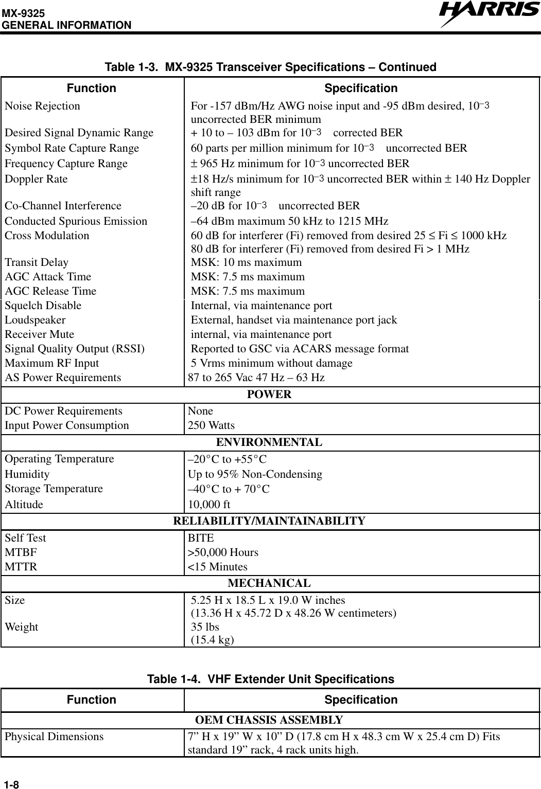
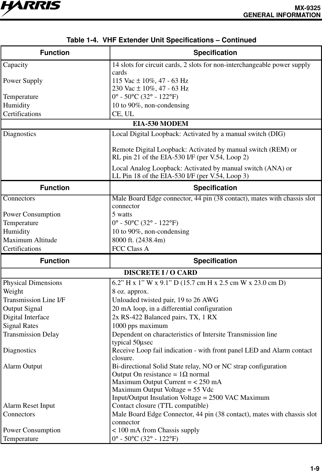
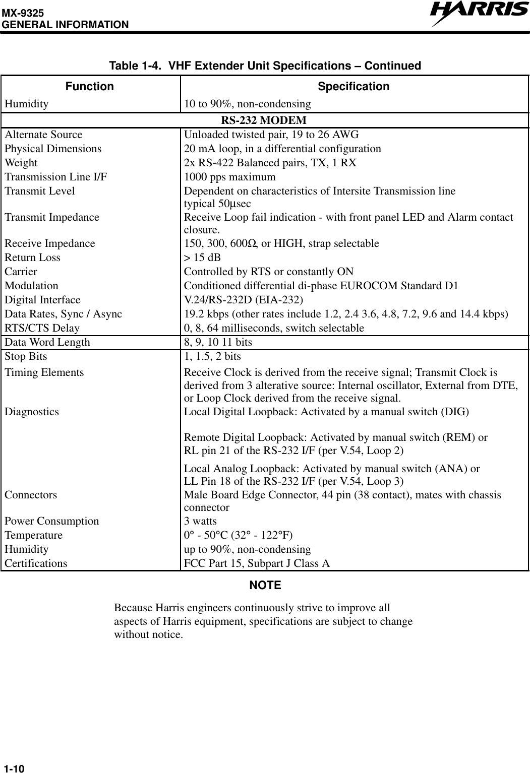
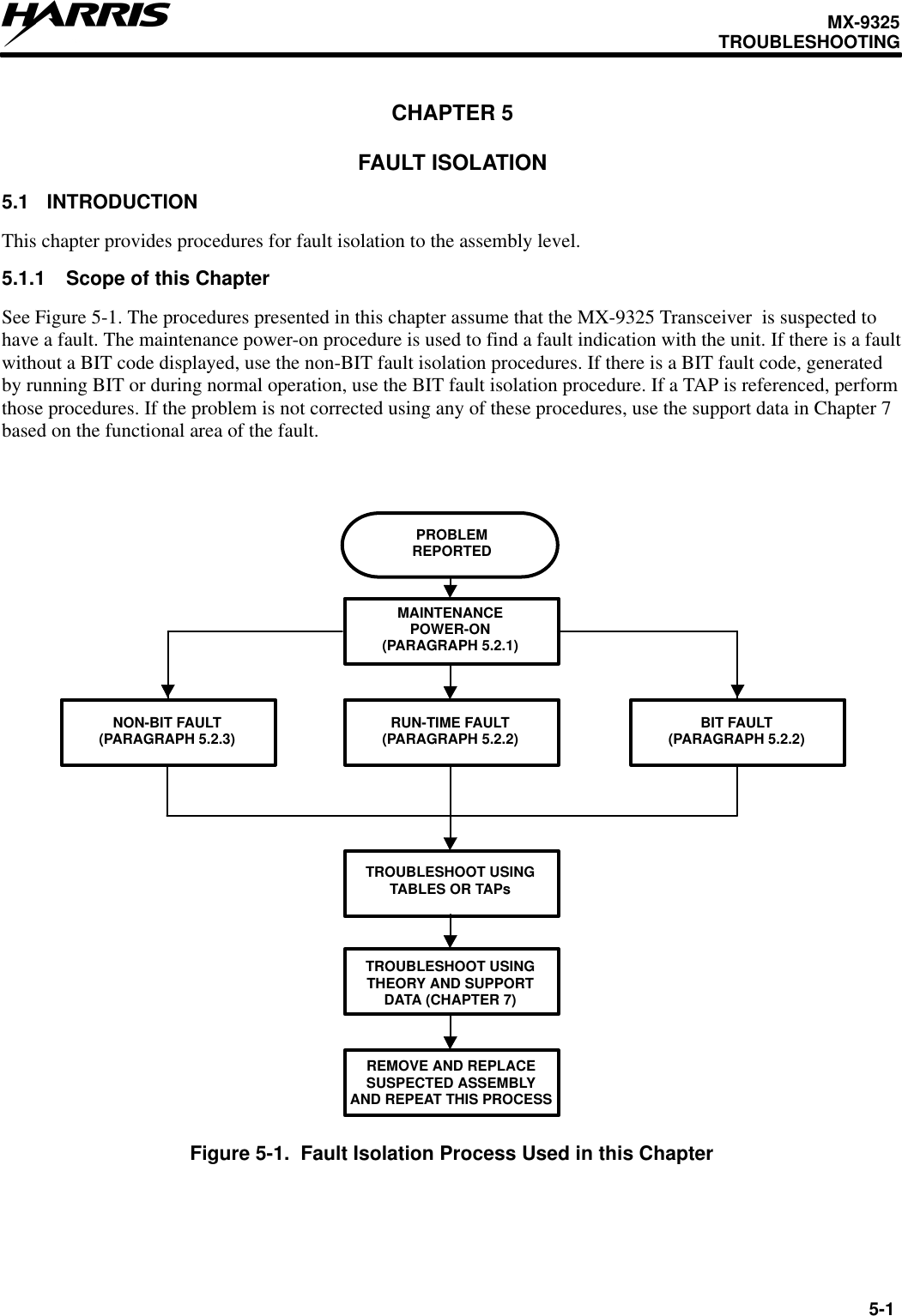
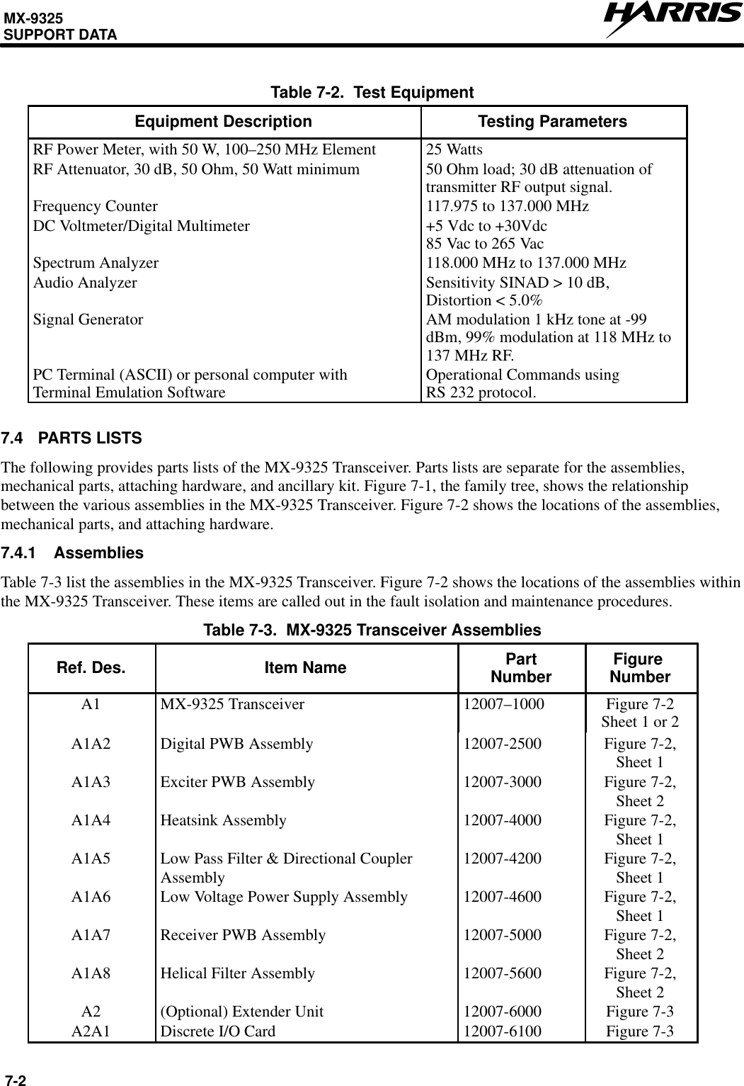
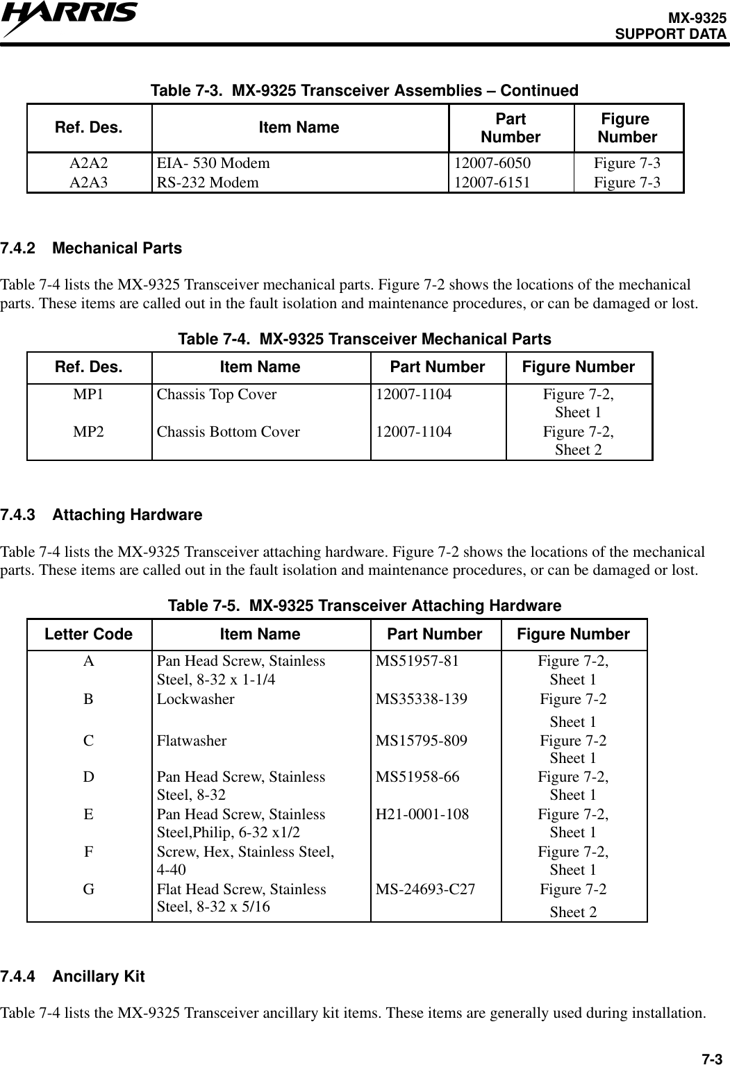
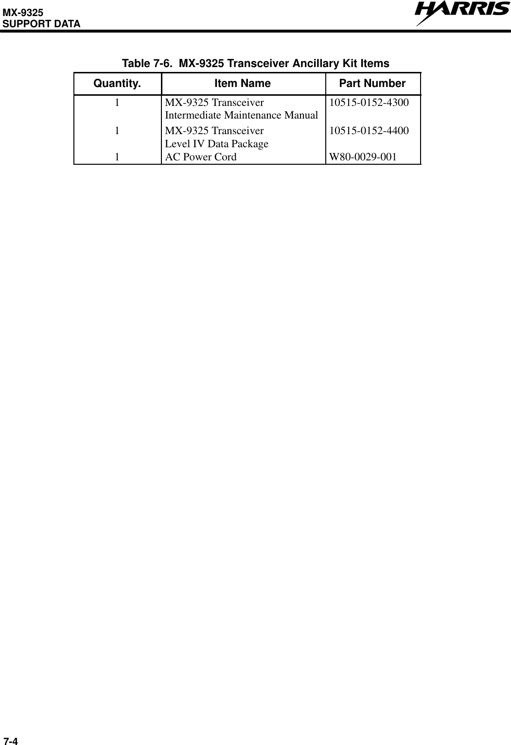
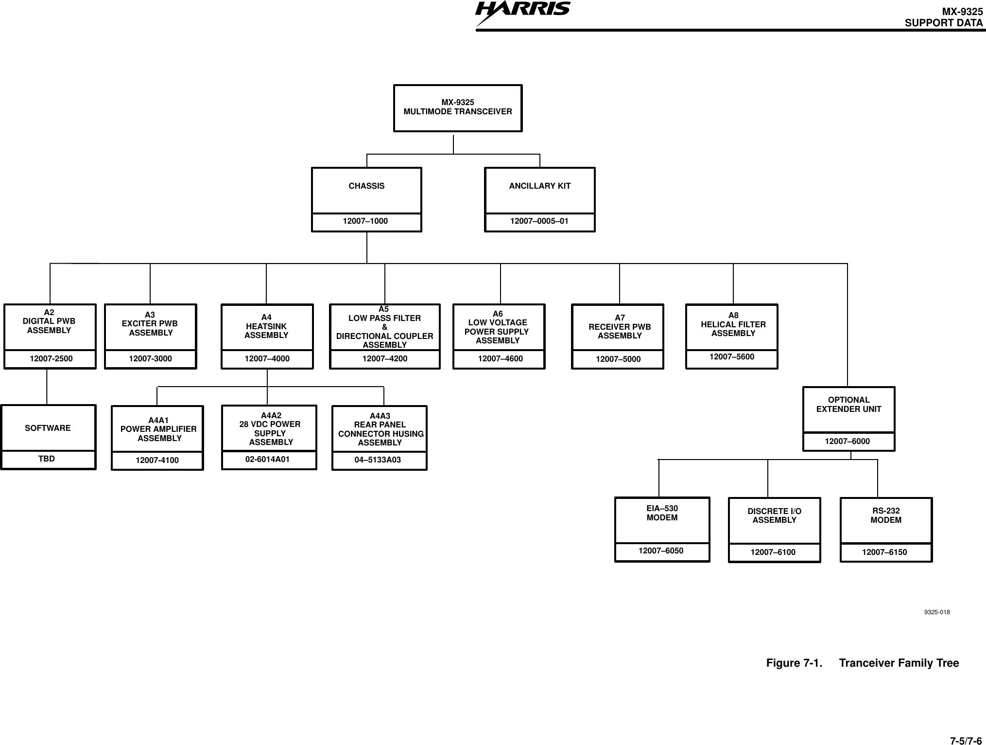
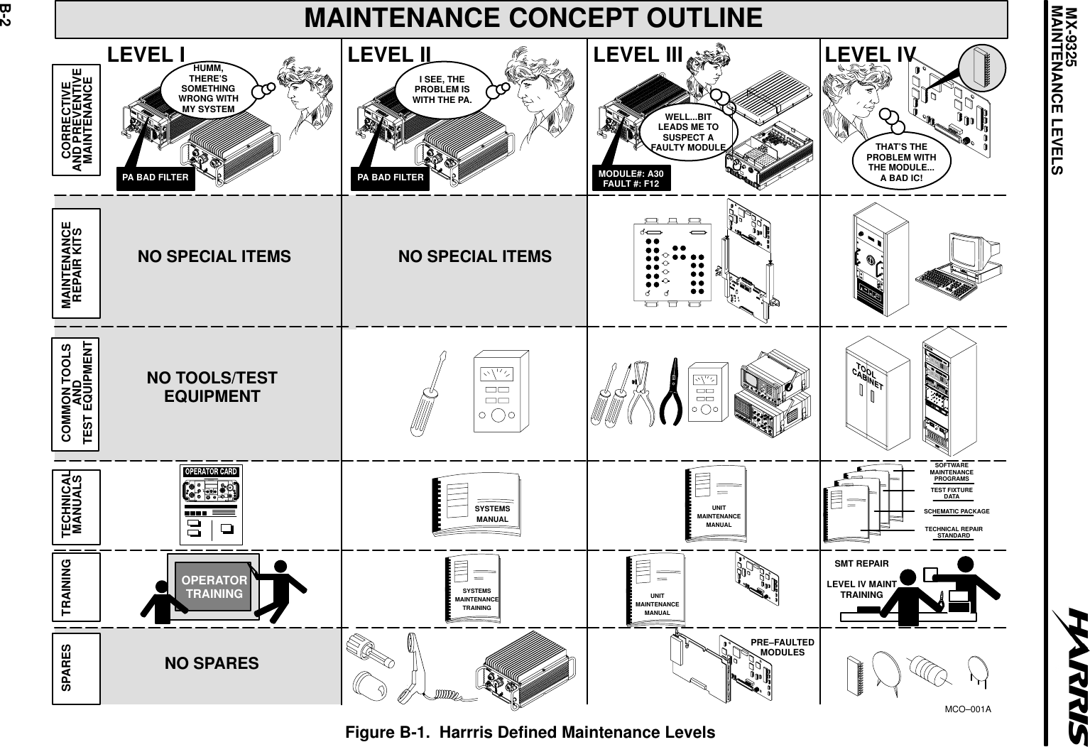
Harris RF Communications Division MX-9325 Multimode data transceiver User Manual in PDF format
Harris Corporation RF Communications Division Multimode data transceiver in PDF format
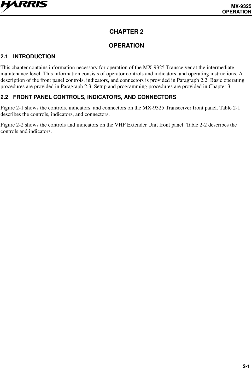
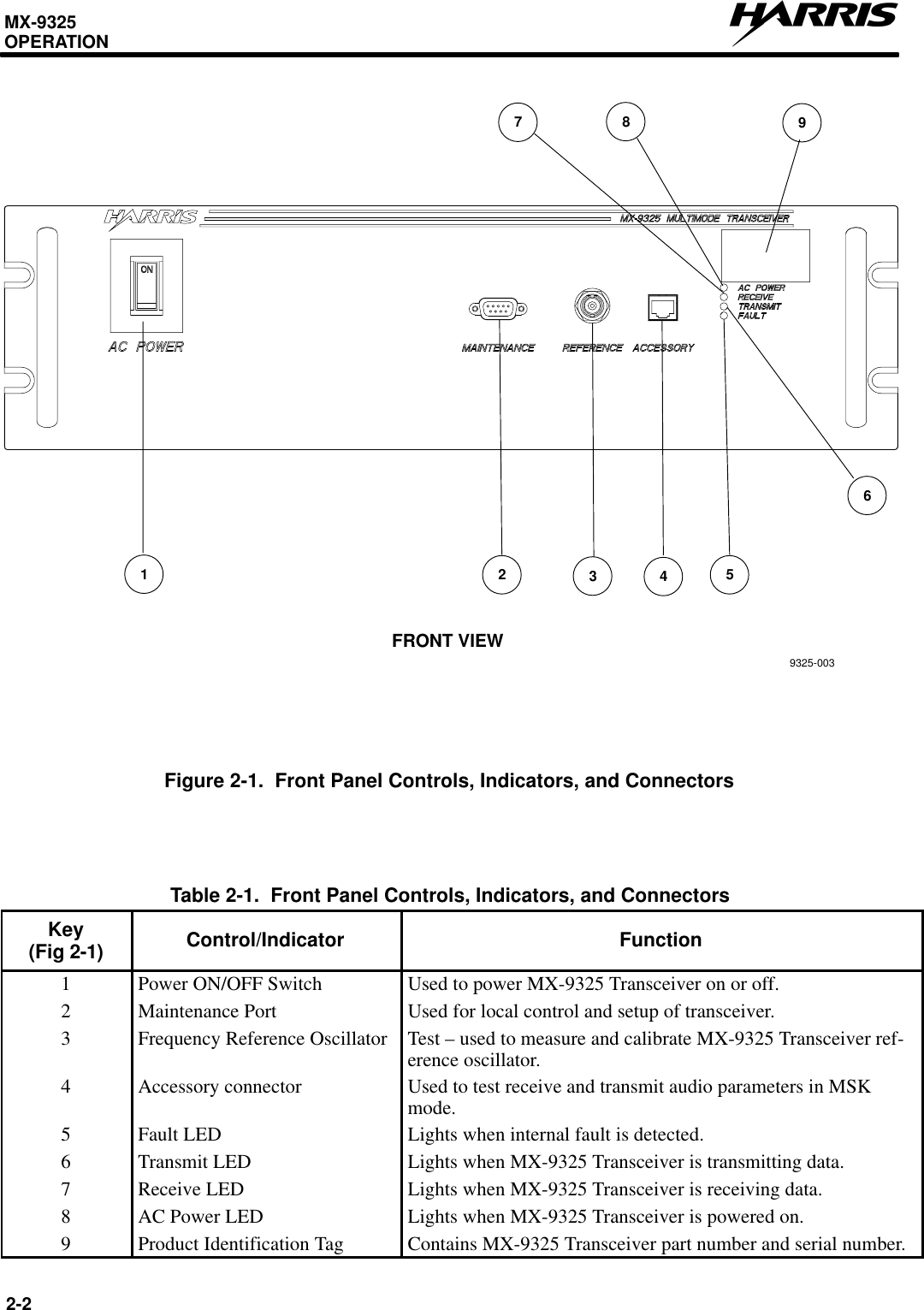
UserManual.wiki
>
Harris RF Communications Division
>
MX 9325 User Manual
user manual in PDF format
Navigation menu
Upload a User Manual
Namespaces
Wiki Guide
HTML
PDF
Info
Views
User Manual
Discussion / Help
Navigation

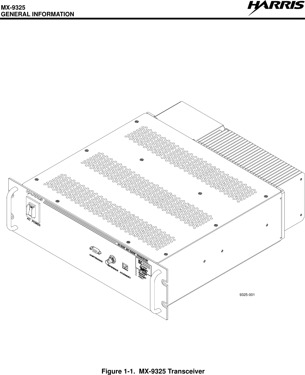
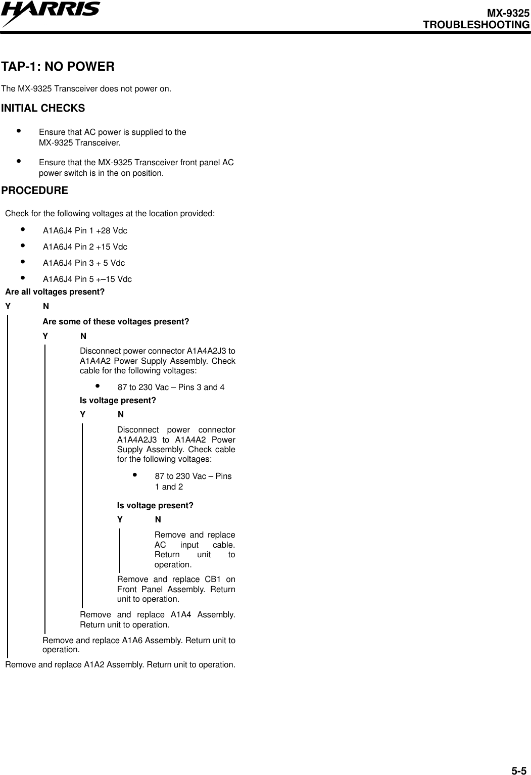
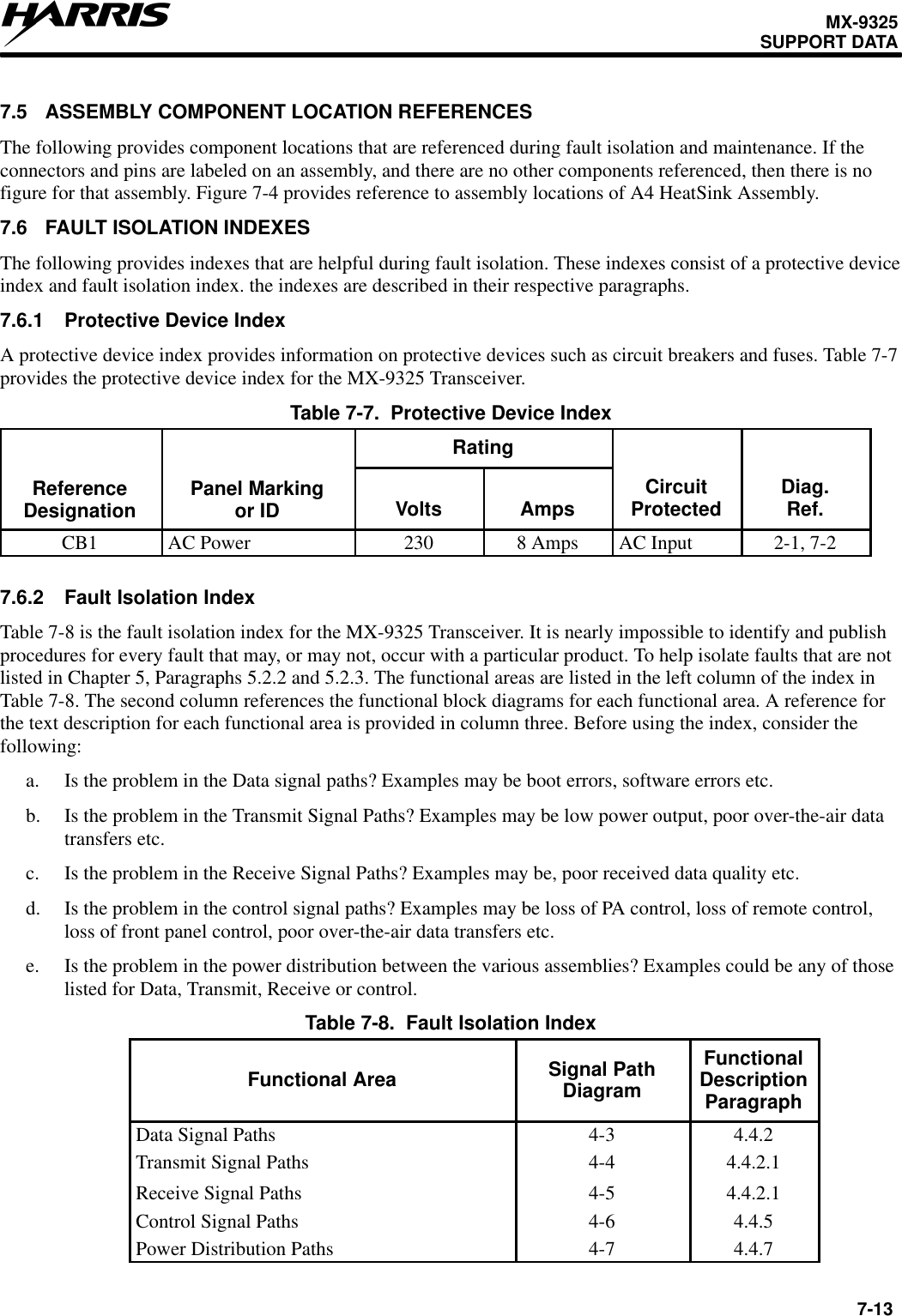
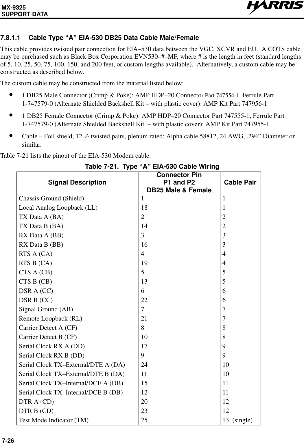
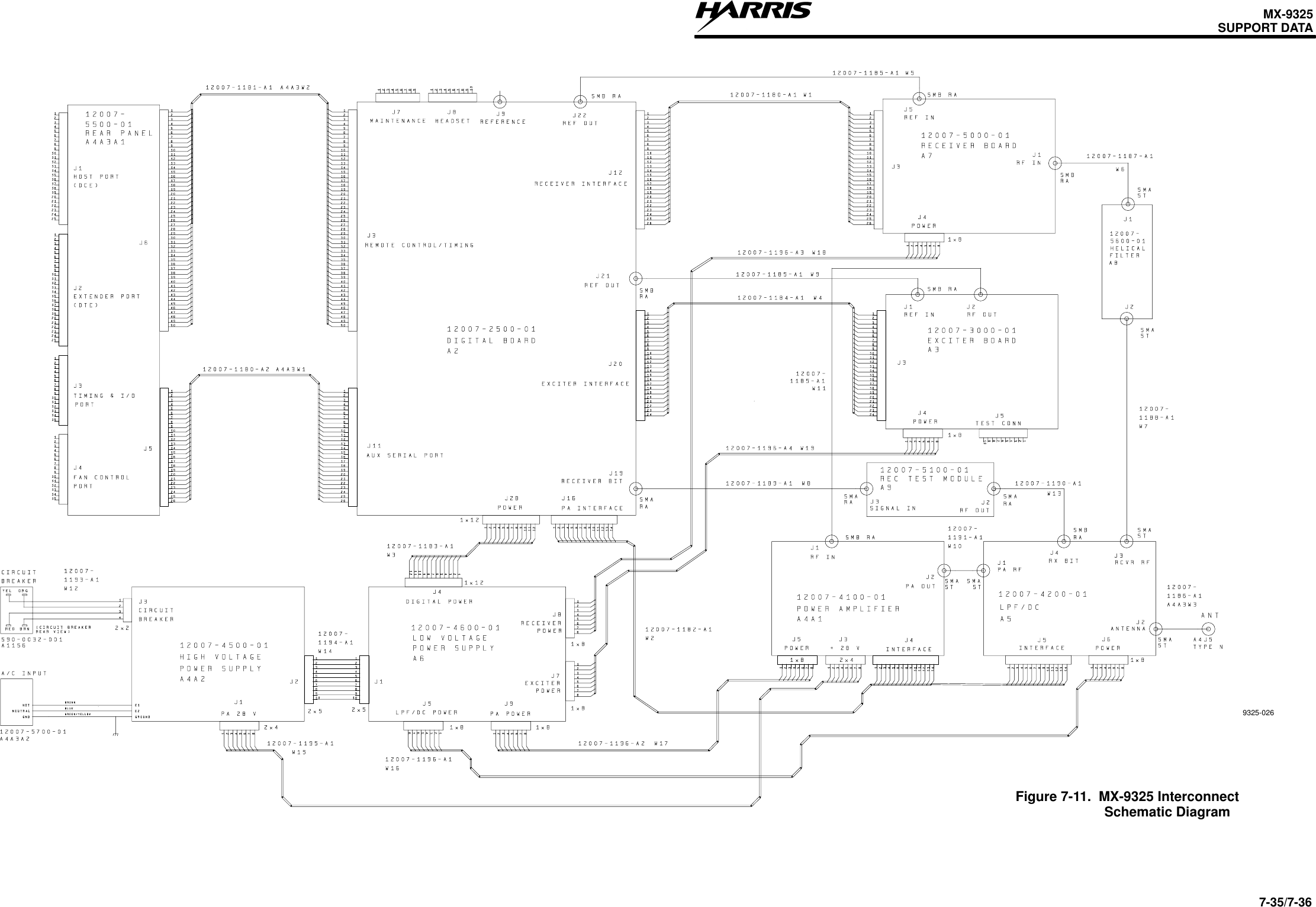
![MX-9325TROUBLESHOOTING5-3Example 1: Fault Code [00000014] indicates the Exciter Failure and Directional Coupler Failure.Example 2: Fault Code [0000000A] indicates the 28 Volt Power Supply Failure and Power Amplifier Failure.After replacing or repairing the suspected cause of the fault, execute BIT, to see whether the original fault hasbeen eliminated. If the actions do not correct the problem, proceed to the troubleshooting index in Paragraph7.6.2.Table 5-2. BIT Fault Codes, Descriptions, and Suspected AssembliesFault Code Fault Text Suspect SRU (Prioritized)00000001 Low Voltage Power Supply Failure AC Input Voltage,A1A4, A1A600000002 28 Volt Power Supply Failure AC Input Voltage, A1A4,A1A600000004 Directional Coupler Failure A1A5, A1A2, Antenna00000008 Power Amplifier Failure A1A4,A1A300000010 Exciter Failure A1A3, A1A4, A1A6, A1A200000020 Receiver Failure A1A7, A1A4, A1A6, A1A200000040 Digital Processor Failure A1A2, A1A4, A1A600000080 Unused Unused00000100 Power Amplifier Heat Sink Low Temp A1A4, A1A200000400 Cooling Fan B N/A00000200 Power Amplifier Heat Sink High Temp A1A4, A1A6, A1A200000800 Cooling Fan A N/A00001000 Rx Sensitivity Low Antenna, A1A5, A1A7, A1A200002000 Power Supply Heat Sink Low Temp A1A4, A1A200004000 Power Supply Heat Sink High Temp A1A4, A1A200008000 System Boot Error A1A25.2.3 Non-BIT Fault IsolationTable 5-3 is a list of the non-BIT fault symptoms. Next to the symptom observed is a reference to therecommended action to take. When the recommended action is to remove and replace assemblies, replace theassemblies one at a time in the order listed, testing the UUT (repeat Paragraph 5.2.1) after replacing eachassembly. Chapter 6, Table 6-1, references the assembly removal and replacement procedures. When therecommended action is to perform a TAP, proceed to the specified TAP. Refer to Paragraph 5.2.5 for more TAPinformation. If the actions do not correct the problem, proceed to the fault isolation support data in Chapter 7.Table 5-3. Non-BIT Fault SymptomsSymptom Observed ProbableArea Suggested SRUMX-9325 Transceiver does not power up. Power Supply Proceed to TAP-1. Paragraph 5.2.5.No RF output Transmit Signal Path A1A2, A1A3, A1A4, A1A5Weak RF output Transmit Signal Path A1A2, A1A3, A1A4, A1A5No Receiver Signal Receive Signal Path A1A5, A1A8, A1A7, A1A2Weak Receiver Signal Receive Signal Path A1A5, A1A8, A1A7, A1A2Loss of PC/terminal control Data Signal Path A1A2, PC/Terminal](https://usermanual.wiki/Harris-RF-Communications-Division/MX-9325/User-Guide-107097-Page-59.png)
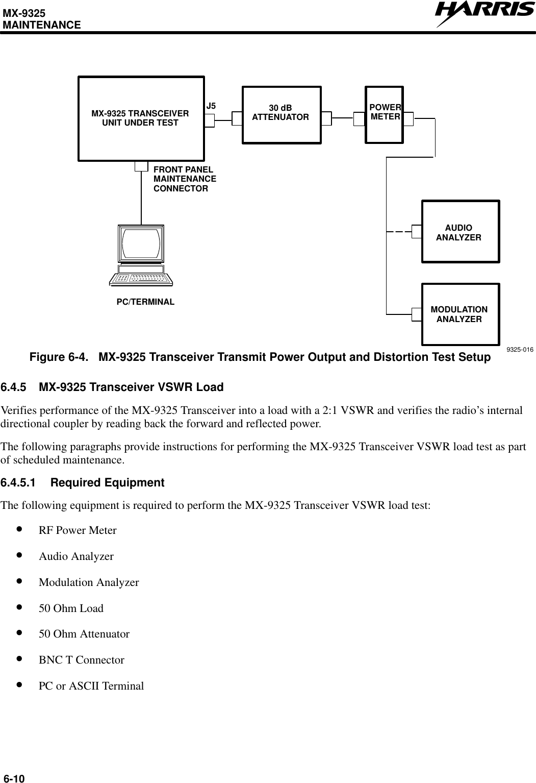
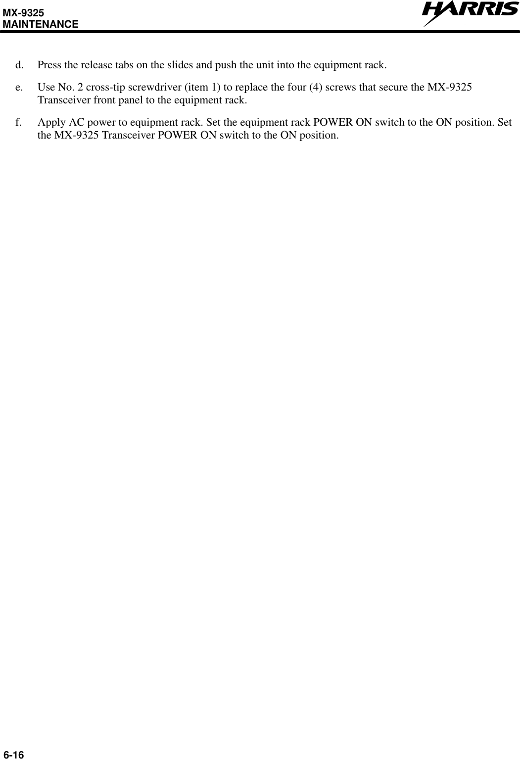
![MX-9325INSTALLATION8-1CHAPTER 8INSTALLATION8.1 INTRODUCTIONThis chapter provides installation instructions for the MX-9325 Transceiver. Paragraph 8.2 providesrecommendations and Paragraph 8.3 provides unpacking and repacking guidelines. Paragraph 8.4 provides thestep-by-step installation procedures. Paragraph 8.5 provides post-installation procedures which consist of checks,setup, and operational tests, all of which should be performed after installation.8.2 INSTALLATION RECOMMENDATIONSThe information contained here provides general guidelines for installing the System. Read this chapter in itsentirety before beginning installation.8.2.1 Selection of Physical LocationWhen choosing a location, become familiar with the dimensions listed in Paragraphs 8.2.2 through 8.5.3. Takeinto account the following:•Location accommodates dimensions shown on Figure 8-1.•Room for maintenance personnel to access cabling and connectors.•Room for proper ventilation (approximately 2 in [5.8 cm] around MX-9325 Transceiver chassis).](https://usermanual.wiki/Harris-RF-Communications-Division/MX-9325/User-Guide-107097-Page-123.png)
![MX-9325INSTALLATION8-38.2.2 GroundingWhen installing the MX-9325 Transceiver into a system rack, perform the following:WARNINGInadequate or defective grounding presents a personnel hazardthat could result in injury or death.CAUTIONInadequate or defective grounding could damage the equipment.•Connect ground braid to the ground stud provided on the rear panel.•Use as thick a braid as possible.•Make sure braid is short (typically less than six feet [182.9 cm]).•Connect other end of braid to TBD.•TBD In arid climates, use ground radials.8.2.3 Power RequirementsThe MX-9325 Transceiver is designed to be powered from a 115 Vac or 230 Vac single phase source as listed inChapter 1, Paragraph 1.7. When the MX-9325 Transceiver is supplied as part of a system designed by Harris,refer to the system documentation. If installing the MX-9325 Transceiver in a customer specific application, usethe supplied AC power cable listed in Chapter 7, Paragraph 7.4.4.8.2.4 EnvironmentalThe MX-9325 Transceiver is designed to function in the environments listed in Chapter 1, Paragraph 1.7.8.2.5 Access Clearance and Ventilation RequirementsWhen the MX-9325 Transceiver is supplied as part of a system designed by Harris, refer to the systemdocumentation. If installing the MX-9325 Transceiver in a customer specific application, make sure there isapproximately 2-Inches (5.8 cm) around chassis.8.2.6 Antenna ConsiderationsTo Be Determined.8.2.7 Tools and Materials RequiredA typical installation requires standard tools listed in Chapter 7, Paragraph 7.3.](https://usermanual.wiki/Harris-RF-Communications-Division/MX-9325/User-Guide-107097-Page-125.png)
![TECHNICAL PUBLICATIONEVALUATION FORMTo the User of this Instruction Manual:HARRIS Corporation, RF Communications Division continually evaluates its technical publications forcompleteness, technical accuracy, and organization. You can assist in this process by completing andreturning this form. Please specify section, page number, figure or table number where applicable.MANUAL TITLE:MANUAL NUMBER: REVISION: COVER DATE:GENERAL EXCELLENT GOOD FAIR POORTEXT [ ] [ ] [ ] [ ]SETUP/ALIGNMENT INST. [ ] [ ] [ ] [ ]TROUBLESHOOTING INST. [ ] [ ] [ ] [ ]TABLES [ ] [ ] [ ] [ ]ILLUSTRATIONS [ ] [ ] [ ] [ ]PARTS LISTS [ ] [ ] [ ] [ ]SCHEMATIC DIAGRAMS [ ] [ ] [ ] [ ]GENERAL COMMENTS: Please include your suggestions for improvements to the manual. Specify chapter,page, paragraph, figure number, or table number as applicable. Attach examples or extra pages if morespace is needed.CHAPTER EXCELLENT GOOD FAIR POORINTRODUCTION/GENERAL INFORMATION [ ] [ ] [ ] [ ]OPERATION [ ] [ ] [ ] [ ]FUNCTIONAL DESC/THEORY OF OPERATION [ ] [ ] [ ] [ ]SCHEDULED MAINTENANCE [ ] [ ] [ ] [ ]TROUBLESHOOTING [ ] [ ] [ ] [ ]CORRECTIVE MAINTENANCE [ ] [ ] [ ] [ ]DOCUMENTATION [ ] [ ] [ ] [ ]INSTALLATION [ ] [ ] [ ] [ ]ACCESSORIES [ ] [ ] [ ] [ ]CUT HERE LEAF-043A MAP](https://usermanual.wiki/Harris-RF-Communications-Division/MX-9325/User-Guide-107097-Page-146.png)