Harris RF Communications Division MX-9325 Multimode data transceiver User Manual in PDF format
Harris Corporation RF Communications Division Multimode data transceiver in PDF format
user manual in PDF format

PUBLICATION NUMBER: 10515-0152-4300
JUNE 2000
Rev. 02
Air Traffic Control Communications
next level solutions
MX-9325
TRANSCEIVER
INTERMEDIATE MAINTENANCE
MANUAL
The material contained herein is subject to U.S. export approval.
No export or re-export is permitted without written approval from the U.S. Government.

LIMITED ONE YEAR WARRANTY
HARRIS CORPORATION (RF COMMUNICATIONS DIVISION)
FROM HARRIS TO YOU – This warranty is extended to the original buyer and applies to all Harris Corporation, RF
Communications Division equipment purchased and employed for the service normally intended, except those products
specifically excluded.
WHAT WE WILL DO – If your Harris Corporation, RF Communications Division equipment purchased from us for use outside the
United States fails in normal use because of a defect in workmanship or materials within one year from the date of shipment, we
will repair or replace (at our option) the equipment or part without charge to you, at our factory. If the product was purchased for
use in the United States, we will repair or replace (at our option) the equipment or part without charge to you at our Authorized Repair
Center or factory.
WHAT YOU MUST DO – You must notify us promptly of a defect within one year from date of shipment. Assuming that Harris
concurs that the complaint is valid, and is unable to correct the problem without having the equipment shipped to Harris:
•Customers with equipment purchased for use outside the United States will be supplied with information for the return
of the defective equipment or part to our factory in Rochester, NY, U.S.A., for repair or replacement. You must prepay
all transportation, insurance, duty and customs charges. We will pay for return to you of the repaired/replaced equipment
or part, C.I.F. destination; you must pay any duty, taxes or customs charges.
•Customers with equipment purchased for use in the United States must obtain a Return Authorization Number, properly
pack, insure, prepay the shipping charges and ship the defective equipment or part to our factory or to the Authorized
Warranty Repair Center indicated by us.
Harris Corporation Telephone: (716) 244-5830
RF Communications Division Fax: 716-242-4755
Customer Service http://www.harris.com
1680 University Avenue
Rochester, NY 14610, U.S.A.
Harris will repair or replace the defective equipment or part and pay for its return to you, provided the repair or replacement is due
to a cause covered by this warranty.
WHAT IS NOT COVERED – We regret that we cannot be responsible for:
•Defects or failures caused by buyer or user abuse or misuse.
•Defects or failures caused by unauthorized attempts to repair or alter the equipment in any way.
•Consequential damages incurred by a buyer or user from any cause whatsoever, including, but not limited to
transportation, non-Harris repair or service costs, downtime costs, costs for substituting equipment or loss of anticipated
profits or revenue.
•The performance of the equipment when used in combination with equipment not purchased from Harris.
•HARRIS MAKES NO OTHER WARRANTIES BEYOND THE EXPRESS WARRANTY AS CONTAINED HEREIN. ALL
EXPRESS OR IMPLIED WARRANTIES OF FITNESS FOR A PARTICULAR PURPOSE OR MERCHANTABILITY ARE
EXCLUDED.
SERVICE WARRANTY – Any repair service performed by Harris under this limited warranty is warranted to be free from defects
in material or workmanship for sixty days from date of repair. All terms and exclusions of this limited warranty apply to the service
warranty.
IMPORTANT – Customers who purchased equipment for use in the United States must obtain a Return Authorization Number
before shipping the defective equipment to us. Failure to obtain a Return Authorization Number before shipment may result in a
delay in the repair/replacement and return of your equipment.
IF YOU HAVE ANY QUESTIONS – Concerning this warranty or equipment sales or services, please contact our Customer Service
Department.

PUBLICATION NUMBER: 10515-0152-4300
JUNE 2000
Rev. 02
HARRIS CORPORATION RF COMMUNICATIONS DIVISION
1680 University Avenue Rochester, New York 14610-1887 USA
Tel: 716-244-5830. Fax: 716-242-4755. http://www.harris.com
MX-9325
TRANSCEIVER
The material contained herein is subject to U.S. export approval. No export or
re-export is permitted without written approval from the U.S. Government.
Information and descriptions contained herein are the property of Harris Corporation. Such information
and descriptions may not be copied or reproduced by any means, or disseminated or distributed without
the express prior written permission of Harris Corporation, RF Communications Division, 1680 University
Avenue, Rochester, New York 14610-1887.
Copyright 2000
By Harris Corporation
All Rights Reserved
Firmware Release: rev. TBD
MX-9325
ii
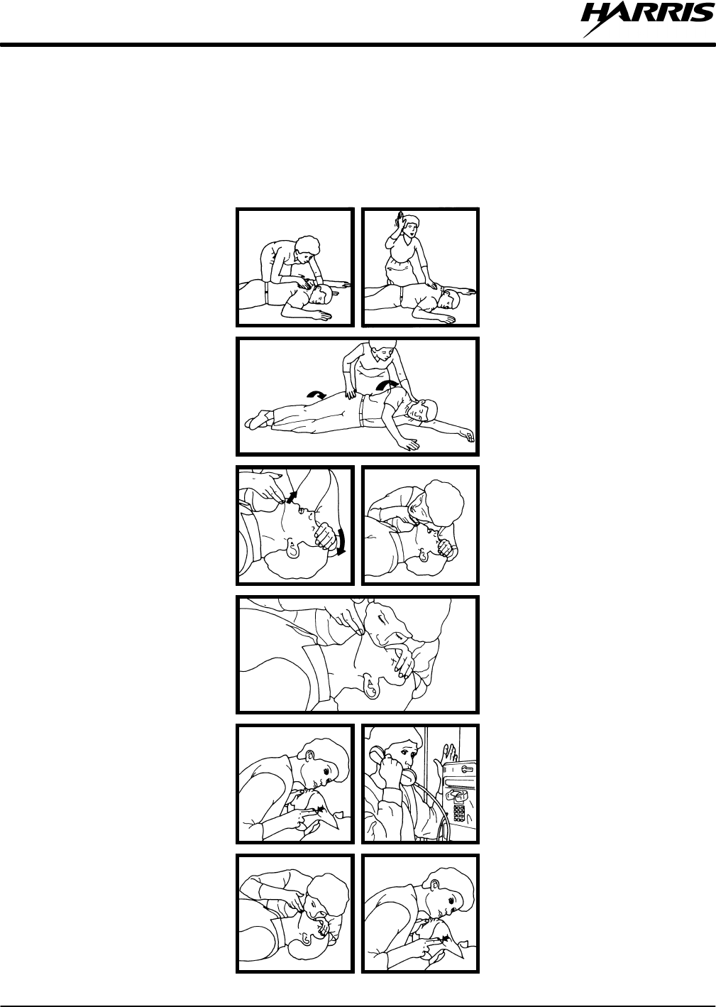
For more information about these and other life–saving techniques, contact your Red Cross chapter for training.
“When Breathing Stops” reproduced with permission from an American Red Cross Poster.
When an Adult Stops Breathing
Does the Person
Respond?
Tap or gently shake
victim.
Shout, “Are you OK?”
1
Roll Person
Onto Back
Roll victim toward you
by pulling slowly.
3
Open Airway
Tilt head back and lift
chin.
4
Give 2 Full
Breaths
Keep head tilted back.
Pinch nose shut.
Seal your lips tight
around victim’s mouth.
Give 2 full breaths for
1 to 1-1/2 seconds each.
6
Check for Pulse
at Side of Neck
Feel for pulse for
5 to 10 seconds.
7
Begin Rescue
Breathing
Keep head tilted back.
Lift chin.
Pinch nose shut.
Give 1 full breath
every 5 seconds.
Look, listen, and feel for
breathing between breaths.
9
Shout, “Help!”
Call people who can
phone for help.
2
Check for
Breathing
Look, listen, and feel
for breathing for
3 to 5 seconds.
5
Phone
for Help
Send someone to call
an ambulance.
8
Recheck Pulse
Every Minute
Keep head tilted back.
Feel for pulse for
5 to 10 seconds.
If victim has pulse but is
not breathing, continue
rescue breathing. If no
pulse, begin CPR.
10
WARNING
DO NOT attempt to perform the rescue breathing techniques provided
on this page, unless certified. Performance of these techniques by
uncertified personnel could result in further injury or death to the victim.

MX-9325
SAFETY SUMMARY
xi
SAFETY SUMMARY
1. INTRODUCTION
All operators and maintenance personnel must observe the following safety precautions during operation and
maintenance of this equipment. Specific warnings and cautions are provided in the manual and at the end of this
Safety Summary. Warnings, Cautions, and Notes appear before various steps in the manual and will be used as
follows:
•WARNING –Used when injury or death to personnel and damage to equipment is possible
•CAUTION –Used when there is a possibility of damage to equipment
•NOTE –Used to alert personnel to a condition that requires emphasis
2. PERSONNEL AND EQUIPMENT SAFETY
Basic safety precautions consider factors involved in protecting personnel from injury or death. Electrical,
mechanical, EMR, material, or chemical hazards are the most common types of hazards found in electronic
equipment. The following are types of hazards that may exist:
ELECTRICAL –Hazardous voltage and current levels may exist throughout the equipment. Contact
with these hazards could cause electrocution, electrical shock, burns, or injury due to
involuntary reflexes of the body.
MECHANICAL –Mechanical hazards are created when heavy assemblies and components must be
removed and replaced. Moving parts (such as fan blades) and hot surfaces are
potential mechanical hazards.
THERMAL –Burn hazards may exist in the equipment that could cause personal injuries and/or
serious equipment damage. Internal surfaces of the equipment may be in excess of
65°C, the point at which personnel could be burned. Extreme caution should be used
when working with any hot assemblies (for example, power supply or power amplifier
assemblies). Physical injury or damage may result to personnel and/or equipment as a
result of a reflex action to a burn.
CHEMICAL –Chemicals or materials used for servicing the equipment may present potential
hazards. Many chemical agents, such as cleaners and solvents, may be toxic, volatile,
or flammable. If used incorrectly, these agents can cause injury or death.
EMR –Overexposure to electromagnetic radiation results from amplified radio frequencies
that may produce a health hazard.

MX-9325
SAFETY SUMMARY
xii
3. OPERATIONAL AND MAINTENANCE SAFETY GUIDELINES
Good safety discipline is critical to prevent injury to personnel. All other safety measures are useless if personnel
do not observe the safety precautions and do not follow safety disciplines. Once aware of a hazard, personnel
should ensure that all other personnel are aware of the hazard. The following basic safety disciplines are stressed:
a. Read a procedure entirely before performing it. Personnel must always perform each assigned task in a
safe manner.
b. Prior to applying equipment power after maintenance, personnel must ensure that all unsecured hand
tools and test equipment are disconnected from the serviced/maintained equipment and properly stored.
c. Power to the equipment must be removed before a piece of equipment is removed.
d. Extreme care must be used when adjusting or working on operating equipment. Voltages in excess of
70 V or current sources in excess of 25 A are covered with barriers. Barriers include warning information
about the hazard encountered upon barrier removal.
e. Personnel must react when someone is being electrically shocked. Perform the following steps:
1. Shut off power.
2. Call for help.
3. Administer first aid if qualified.
Under no circumstances should a person come directly in contact with the body unless the power has
been removed. When immediate removal of the power is not possible, personnel must use a
non-conductive material to try to jolt or pry the body away from the point of shock.
f. Personnel should work with one hand whenever possible to prevent electrical current from passing
through vital organs of the body. In addition, personnel must never work alone. Someone must be
available in the immediate area to render emergency first aid, if necessary.
g. Lifting can cause injury. Items weighing more than 37 pounds must be lifted by two or more people.
h. Some electrolytic capacitors contain aluminum oxide or tantalum. If connected incorrectly, the capacitor
will explode when power is applied. Extreme care must be used when replacing and connecting these
capacitors. The capacitor terminals must always be connected using the correct polarity: positive to
positive and negative to negative.

MX-9325
SAFETY SUMMARY
xiii
The next section contains general safety precautions not directly related to specific procedures or equipment.
These precautions are oriented toward the maintenance technician. However, all personnel must understand and
apply these precautions during the many phases of operation and maintenance of the equipment. The following
precautions must be observed:
DO NOT SERVICE EQUIPMENT ALONE
Never work on electrical equipment unless another person familiar with the operation and hazards of the
equipment is near. When the maintenance technician is aided by operators, ensure that operators are aware of
the hazards.
GROUNDING
Always ensure that all equipment and assemblies are properly grounded when operating or servicing.
TURN OFF POWER AND GROUND CAPACITORS
Whenever possible, power to equipment should be turned off before beginning work on the equipment. Be
sure to ground all capacitors that are potentially dangerous.
KEEP AWAY FROM LIVE CIRCUITS
Operators and maintainers must observe all safety regulations at all times. Do not change components or
make adjustments inside equipment with a high voltage supply on unless required by the procedure. Under
certain conditions, dangerous potentials may exist in circuits with power controls off, due to charges retained
by capacitors.
DO NOT BYPASS INTERLOCKS
Do not bypass any interlocks unnecessarily. If it is necessary to employ an interlock bypass for equipment
servicing, use extreme care not to come in contact with hazardous voltages.
USE CARE HANDLING HEAVY EQUIPMENT
Never attempt to lift large assemblies or equipment without knowing their weight. Use enough personnel or a
mechanical lifting device to properly handle the item without causing personal injury.
HEED WARNINGS AND CAUTIONS
Specific warnings and cautions are provided to ensure the safety and protection of personnel and equipment.
Be familiar with and strictly follow all warnings and cautions on the equipment and in technical manuals.
PROTECTIVE EYEWEAR
All personnel must wear protective eyewear when servicing or maintaining equipment. Protective eyewear
must be worn at all times when using tools.
MX-9325
SAFETY SUMMARY
xiv
4. PROTECTION OF STATIC-SENSITIVE DEVICES
Diode input-protection is provided on all CMOS devices. This protection is designed to guard against adverse
electrical conditions such as electrostatic discharge. Although most static-sensitive devices contain protective
circuitry, several precautionary steps should be taken to avoid the application of potentially damaging
voltages to the inputs of the device.
To protect static-sensitive devices from damage, the following precautions should be observed.
a. Keep all static-sensitive devices in their protective packaging until needed. This packaging is
conductive and should provide adequate protection for the device. Storing or transporting these
devices in conventional plastic containers could be destructive to the device.
b. Disconnect power prior to insertion or extraction of these devices. This also applies to PWBs
containing such devices.
c. Double check test equipment voltages and polarities prior to conducting any tests.
d. Avoid contact with the leads of the device. The component should always be handled carefully by
the ends or side opposite the leads.
e. Avoid contact between PWB circuits or component leads and synthetic clothing.
f. Use only soldering irons and tools that are properly grounded. Ungrounded soldering tips or tools
can destroy these devices. SOLDERING GUNS MUST NEVER BE USED.
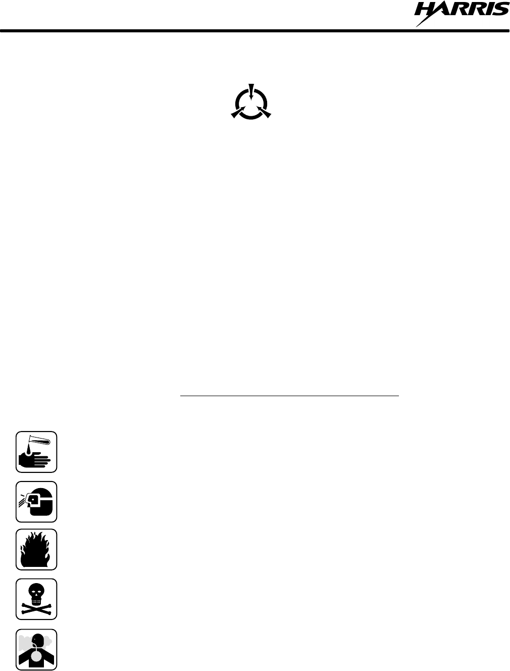
5. EXPLANATION OF HAZARD SYMBOLS
The symbol of drops of a liquid onto a hand shows that the material will cause burns or
irritation of human skin or tissue.
The symbol of a person wearing goggles shows that the material will injure your eyes.
The symbol of a flame shows that a material can ignite and burn you.
The symbol of a skull and crossbones shows that a material is poisonous or a danger to life.
The symbol of a human figure in a cloud shows that vapors of a material present danger to your
life or health.
MX-9325
GENERAL INFORMATION
MX-9325
TRANSCEIVER
MX-9325
GENERAL INFORMATION
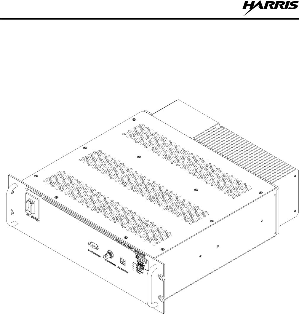
Figure 1-1. MX-9325 Transceiver
9325-001

MX-9325
GENERAL INFORMATION
1-1
CHAPTER 1
GENERAL INFORMATION
1.1 INTRODUCTION
This manual provides the technician with all technical information required to support level III maintenance as
described in Appendix B.
The overall intent of this manual is to help the technician expedite repair of the unit in a reasonable amount of
time, resulting in reduced down-time and increased system availability. Detailed information that is useful to the
technician is provided: configuration, specifications, fault isolation, repair, tools, test equipment, and functional
descriptions of the assemblies. A glossary of terms is also provided in Appendix A.
1.2 WARRANTY
For warranty information refer to the inside front cover of this manual.
NOTE
Contractual agreements may supersede standard warranty. Refer
to contract agreement for additional warranty information.
1.3 GENERAL EQUIPMENT DESCRIPTION
1.3.1 MX-9325 Transceiver
Figure 1-1 shows the MX-9325 Transceiver.
The MX-9325 Transceiver is a rack-mounted, fully programmable unit. The MX-9325 Transceiver operates as a
double sideband AM-MSK analog data Transceiver or as a D8PSK digital-data transceiver. The MX-9325
Transceiver yields a 25-Watt power output that covers the frequency range of 118.000 to 136.975 MHz with 25
kHz spacing between channels. All programmable features and functions are controlled via asynchronous serial
port on front panel from a PC or an ASCII terminal. The MX-9325 Transceiver operates from 87 Vac to 265 Vac,
47 Hz to 63 Hz.
The MX-9325 Transceiver represents a new generation of ground-to-air VHF radio equipment to meet the
demanding needs for ATC communications. This advanced MX-9325 Transceiver is designed to operate in two
modes. As a double sideband AM-MSK analog data transceiver, the MX-9325 Transceiver supports the
requirements for a multiple-mode communications radio for ACARS utilizing an MSK modem integral to the
radio providing all modulation/demodulation and CSMA for media access control. As a D8PSK digital-data
transceiver, the MX-9325 Transceiver supports the following operational requirements:
•Mode 2 ICAO Annex 10, Volume III
•Mode 3 operation per RTCA SC-172, working group 3 MOPS
•EUROCAE working group 47 MOPS
The MX-9325 Transceiver is operated from a VHF Ground Computer (VGC) using ACARS software. For more
information on operations, refer to the VGC and ACARS Operations Manual. Locally the VGC interfaces to the
MX-9325 Transceiver Host Port. Remote operations are controlled using a VGC with an optional VHF Extender
Unit. Refer to Paragraph 1.3.2 for VHF Extender Unit description. The Extender Unit is also required for split site
configuration (MX-9325 Transceiver installed as a separate transmitter and receiver function). Remote control is
via an RS-422 electrical connection using a baud rate up to 192 k baud programmable from the VGC.

MX-9325
GENERAL INFORMATION
1-2
The MX-9325 Transceiver maintains three non-volatile storage areas called Software Banks, to hold downloaded
software data. At any time, two of the banks are considered active and contain valid copies of the MX-9325
Transceiver operating software. This enables the radio to execute the most recent downloaded version of its
software, or to switch to a previously downloaded version via instruction from the VGC. When a MX-9325
transceiver is shipped from the factory, it contains identical versions of software in all software banks, although
only two banks are regarded as containing active software versions.
Another feature of the MX-9325 Transceiver is its BIT capability. BIT self-test routine diagnoses and isolates
faults within the MX-9325 Transceiver to the assembly level. Faults are reported to the MX-9325 Transceiver
front panel fault LED. The fault code is diagnosed at a PC or ASCII terminal connected to the front panel
mounted maintenance port or from the VGC using a BIT command. This feature helps to quickly test and repair
the transceiver. Within the MX-9325 Transceiver BIT, it continuously monitors power supply output, synthesizer
lock status, receiver sensitivity and the PA temperature.
1.3.2 VHF Extender Unit (optional)
Figure 1-2 shows the VHF Extender Unit. The VHF Extender Unit is required for remote and split site
configurations.
The VHF Extender Unit is rack mounted and consists of 14 plug-in card modules and two fused power supplies to
accommodate inputs of 115 or 230 Vac. The VHF Extender Unit is designed to interface signal or multiple
Transceivers to the VGC and to an optional 4 by 4 antenna relay switch that automatically switches the VGC to a
reserved MX-9325 Transceiver during a disabling fault situation.
Using the VHF Extender Unit, the receivers channel busy and the transmitter’s receiver mute differential signal
output lines are extended to the remote site by means of a current loop interface circuit, capable of driving the
required maximum length of hard wire lines between sites. Refer to Chapter 3 for MX-9325 Transceiver
configuration. Refer to Chapter 8 for system interconnect diagrams.
The VHF Extender Unit specifications are included in Table 1-3.
1.3.2.1 VHF Extender Unit Plug-in Module Cards
The VHF Extender Unit uses three types of plug-in module cards. The type and quantity depend on the MX-9325
Transceiver system configuration. The following are the plug-in module card types and configuration when used:
•EIA-530 Modem - A high speed, short range synchronous COTS data modem card. The EIA-530 Modem
is required for each MX-9325 Transceiver to communicate in remote site configuration, quantity 14
maximum. The EIA-530 Modem is utilized to extend the Host Port EIA-serial data interface between the
local site computer or MX-9325 Transceiver and remote site MX-9325 Transceiver.
•Discrete I/O Card - A circuit card containing two (2) discrete control line level converters. The Discrete
I/O Card is required along with each EIA-530 Modem for split site MX-9325 Transceiver configuration,
quantity seven (7) maximum of discreet I/O cards with seven (7) maximum EIA-530 Modems. The
Discrete I/O Card is utilized to extend the transmit mute and receiver channel busy signals between local
and remote site MX-9325 Transceivers to support ACARS and Mode 2 operation. Each board has an
EIA-422 signal level input and output (TX/RX) which is converted to and from differential 20 mA loop
levels for transmission over the intersite lines.
•RS-232 Modem - A low speed, short-range asynchronous COTS data modem card. Required for each
optional antenna relay switch installed. One (1) antenna relay switch accommodates eight (8)
transceivers. The RS-232 Modem is utilized to extend EIA-232 Serial data between VGC and multiple
Transceivers to a 4 by 4 antenna relay switch that automatically switches the VGC to a reserved
MX-9325 Transceiver during a disabling fault situation.

MX-9325
GENERAL INFORMATION
1-3
Refer to Table 1-2 for additional VHF Extender Unit configuration information.
1.3.3 MX-9325 Transceiver Front Panel
See Figure 1-1. The MX-9325 Transceiver front panel provides serial connector for maintenance interface. Also
provided on the front panel, on/off switch, status indication LEDs, reference oscillator test connection and an
accessory connector.
1.3.4 MX-9325 Transceiver Rear Panel
Refer to Chapter 8, Figure 8-2. The MX-9325 Transceiver rear panel provides AC power connector, antenna (RF)
connection, discrete I/O port, extender port, and host (data) port.
1.3.5 VHF Extender Unit Rear Panel
Refer to Chapter 8, Figure 8-3. The VHF Extender Unit rear panel provides 14 snap type terminal block
transmission line connections, 14-dB 25 female data interface connections.
MX-9325
GENERAL INFORMATION
1-4
Figure 1-2. VHF Extender Unit
9325–002
MX-9325
GENERAL INFORMATION
1-5
1.3.6 Mounting
The MX-9325 Transceiver and VHF extender unit are designed to be rack mounted. Refer to Chapter 6 and
Chapter 8 for installation information.
1.3.7 MX-9325 MX-9325 Transceiver Configuration Information
Table 1-1 identifies the MX-9325 Transceiver configuration and part number described in this manual. Table 1-2
identifies the VHF extender unit configurations and part numbers described in this manual. Refer to Chapter 7 for
family tree. For firmware revision of this manual, refer to the title page that appears just after the warranty inside
the front cover.
Table 1-1. MX-9325 Transceiver Configurations
Product Description Part Number
MX-9325 VHF Multimode Transceiver 12007-1000-01
1.3.8 VHF Extender Unit Configuration Information
Table 1-2 identifies the VHF extender unit configurations and part numbers described in this manual. Column one
(1) lists the part number with the last two (2) digits being the number of MX-9325 Transceivers supported. Refer
to Chapter 7 for the family tree. For firmware revision of this manual, refer to the title page that appears just after
the warranty inside the front cover.
Table 1-2. VHS Extender Unit Configurations
Part Number VHF Extender Unit
Configuration Description
Qty
of
EIA-530
Modem
Slot
Position
in use
by
EIA-530
Modem
Qty
of
I/O
Card
Slot
Position
in use
by
I/O
Card
Qty of
RS-232
Modem
Slot
Position
in use
by
RS-232
Modem
12007-6000-001
Thru
12007-6000-014
Remote or Split Site 1 XCVR
Thru
Remote or Split Site 14 XCVR’s
1
thru
14
1
thru
14
0
Thru
0
0
Thru
0
0
Thru
0
0
Thru
0
12007-6000-101
Thru
12007-6000-108
12007-6000-109
Thru
12007-6000-112
Remote Site 1 XCVR 1 Ant. Sw.
Thru
Remote Site 8 XCVR’s 1 Ant. Sw.
Remote Site 9 XCVR’s 2 Ant. Sw.
Thru
Remote Site 12 XCVR’s 2 Ant. Sw.
1
thru
8
9
thru
12
1
thru
8
9
thru
12
0
Thru
0
0
Thru
0
0
Thru
0
0
Thru
0
1
Thru
1
2
Thru
2
14
Thru
14
13,14
Thru
13,14
12007-6000-201
Thru
12007-6000-207
Split Site 1 XCVR
Thru
Split Site 7 XCVR’s
1
thru
7
1
thru
1,3,5,7,9,
11,13
1
Thru
7
2
Thru
2,4,6,8,
10,12,14
0
Thru
0
0
Thru
0
12007-6000-301
Thru
12007-6000-306
Split Site 1 XCVR 1 Ant. Sw.
Thru
Split Site 6 XCVR’s 1 Ant. Sw.
1
thru
6
1
thru
1,3,5,
7,9,11
1
Thru
6
2
Thru
2,4,6,8,10
,12,14
1
Thru
1
14
Thru
14
1.3.8.1 MX-9325 Transceiver Unit Identification
MX-9325 Transceiver identification information is located on the front panel identification tag.
MX-9325
GENERAL INFORMATION
1-6
1.3.8.2 VHF Extender Unit Identification
VHF Extender Unit Identification is located TBD.
1.4 ADDITIONAL ITEMS SHIPPED WITH UNIT
The MX-9325 Transceiver is shipped with an ancillary kit which is listed in Chapter 7, Paragraph 7.4.4.
1.5 REFERENCE DOCUMENTS
Refer to the following documents for additional information on the OEM VHF Extender Unit.
•RAD Data Communications Publication No. 601-200-04/99, ASM-20 Synchronous/Asynchronous Short
Range Modem Installation and Operation manual, April 1999.
•RAD Data communications Website, www.rad.com, September 1999.
•Electronics Industries Association, EIA-530 Standard: High Speed 25-position Interface for Data
Terminal Equipment and Data circuit-Terminating Equipment, 18 March 1987.
•Black Box Corporation, 256-kbps Line-Driver (LDM-256) Cards User Manual, August 1997.
•Black box Corporation, Racknest 2/14 User Manual, March 1997.
•Black Box Corporation, LDM-MR19.2 User Manual, April 1998.
1.6 RECOMMENDED TOOLS AND TEST EQUIPMENT
Tools and test equipment recommended for installing, troubleshooting, and repairing the MX-9325 Transceiver
are listed in Chapter 7, Paragraph 7.3.
1.7 SPECIFICATIONS
Refer to Table 1-3 for MX-9325 Transceiver specifications.
Table 1-3. MX-9325 Transceiver Specifications
Function Specification
GENERAL
Frequency Range 118 MHz to 136.975 MHz
Frequency Tolerance 1 PPM, –20C to +55C, aging 1 ppm per year maximum
Channel Spacing 25 kHz
Tuning Time 100 ms from the receipt of the last bit of the frequency change
command.
Receive to Transmit Turnaround 1 ms after terminating the receive function
Transmit to Receive Turnaround 1 ms after terminating the final information
EMI/EMC Approvals BZT, CE OFCOM and U.S. FCC Class B Operation
Safety Agency Approvals CSA, UL, BSI
BIT DC power supplies, PA temperature, synthesizer lock, receiver
sensitivity
Data Interface Data Port: RS-422 synchronous, rear panel DB-25 with RS-530
connector definition
Maintenance Port: RS-232 asynchronous, up to 192 kbps, via front
panel DB-9 female connector
Modes AM-MSK : Per ARINC Specification 618-2
Mode 2: Per ICAO Annex 10
Mode 3: Per RTCA SC-172 WG3 MOPS

MX-9325
GENERAL INFORMATION
1-7
Table 1-3. MX-9325 Transceiver Specifications – Continued
Function Specification
Channel Statistics SNR,RSSI, Pre-key value, message duration, cumulative receive time,
cumulative standby time.
TRANSMITTER
Output Power MSK: 25 Watts adjustable from 5 to 25 Watts via maintenance port
D8PSK: 25 Watts average
VSWR No degradation for up to 2:1; no damage from infinite VSWR
Duty Cycle 50% Continuous
Harmonic and Spurious Emissions - 80 dBc minimum for all modes
Adjacent Channel Power and Wide-
band Noise MSK: -70 dBc minimum;
D8PSK: Per ICAO Annex 10
Transmitter Time-out Time 5 to 60 seconds, adjustable
Transmitter Keying Via maintenance port for installation setup and test
RF Power Rise time Less that 190 µs (two symbols)
RF Power Release Time Within 190 µs after transmitting the final information symbol
Data Rate MSK: 2400 bps
D8PSK: 31.5 kilobits per second ± 0.005%
Transmitter Pre-key 0 to 190 msec, adjustment via maintenance port 85 msec default
Transmitter Phase and Amplitude
Balance D8PSK: 90±3 degrees phase, and ± 1 dB amplitude maximum
Transit Delay MSK: 10 mS maximum
Frequency Response MSK: 200 Hz to 3600 Hz ± 2 dB
Differential Phase Delay MSK: 20 µS
Audio Distortion MSK: 5%
Modulation Level MSK: adjustable 30 to 95% via maintenance port
Internal Test Signals MSK: 1200 or 2400 Hz individual; random sequence of 1200 Hz and
2400 Hz; 1 kHz
D8PSK: CW carrier, continuous random data
Digital Interface, Data (J3) RS-232 or RS-422
RECEIVER
Sensitivity MSK: - 99 dBm for 10 dB SINAD, 30% AM with 1 kHz modulation
signal;
D8PSK: - 103 dBm for 10– uncorrected BER
IF Selectivity - 6 dB at ± 10kHz; - 80 dB at ± 25 kHz
Adjacent Channel Rejection 44 dB minimum for 10– uncorrected BER (per EUROCAE MOPS)
Spurious Radiation 80 dB minimum
Rejection of Signals in the VHF
Band For -3 dBm interferer (Fi) removed from desired 450 ≤ (Fi) ≤ 2000
kHz, less than 3 dB SINAD degradation;
For 0 dB interferer (Fi) removed from desired Fi ≤2 MHz, less that
3 dB SINAD degradation
Rejection of Signals outside the
VHF Band For signal interferer 0 dB or less within FM broadcast band, no SINAD
degradation.
In-Band Signal Rejection 70 dB minimum for interfering signals spaced greater that 100 kHz
from desired.
FM Broadcast Intermodulation For two interfering signals 0 dB or less within FM broadcast band, no
SINAD degradation.
MX-9325
GENERAL INFORMATION
1-8
Table 1-3. MX-9325 Transceiver Specifications – Continued
Function Specification
Noise Rejection For -157 dBm/Hz AWG noise input and -95 dBm desired, 10–
uncorrected BER minimum
Desired Signal Dynamic Range + 10 to – 103 dBm for 10– corrected BER
Symbol Rate Capture Range 60 parts per million minimum for 10– uncorrected BER
Frequency Capture Range ± 965 Hz minimum for 10– uncorrected BER
Doppler Rate ±18 Hz/s minimum for 10– uncorrected BER within ± 140 Hz Doppler
shift range
Co-Channel Interference –20 dB for 10– uncorrected BER
Conducted Spurious Emission –64 dBm maximum 50 kHz to 1215 MHz
Cross Modulation 60 dB for interferer (Fi) removed from desired 25 ≤ Fi ≤1000 kHz
80 dB for interferer (Fi) removed from desired Fi > 1 MHz
Transit Delay MSK: 10 ms maximum
AGC Attack Time MSK: 7.5 ms maximum
AGC Release Time MSK: 7.5 ms maximum
Squelch Disable Internal, via maintenance port
Loudspeaker External, handset via maintenance port jack
Receiver Mute internal, via maintenance port
Signal Quality Output (RSSI) Reported to GSC via ACARS message format
Maximum RF Input 5 Vrms minimum without damage
AS Power Requirements 87 to 265 Vac 47 Hz – 63 Hz
POWER
DC Power Requirements None
Input Power Consumption 250 Watts
ENVIRONMENTAL
Operating Temperature –20C to +55C
Humidity Up to 95% Non-Condensing
Storage Temperature –40C to + 70C
Altitude 10,000 ft
RELIABILITY/MAINTAINABILITY
Self Test BITE
MTBF >50,000 Hours
MTTR <15 Minutes
MECHANICAL
Size 5.25 H x 18.5 L x 19.0 W inches
(13.36 H x 45.72 D x 48.26 W centimeters)
Weight 35 lbs
(15.4 kg)
Table 1-4. VHF Extender Unit Specifications
Function Specification
OEM CHASSIS ASSEMBLY
Physical Dimensions 7” H x 19” W x 10” D (17.8 cm H x 48.3 cm W x 25.4 cm D) Fits
standard 19” rack, 4 rack units high.

MX-9325
GENERAL INFORMATION
1-9
Table 1-4. VHF Extender Unit Specifications – Continued
Function Specification
Capacity 14 slots for circuit cards, 2 slots for non-interchangeable power supply
cards
Power Supply 115 Vac ± 10%, 47 - 63 Hz
230 Vac ± 10%, 47 - 63 Hz
Temperature 0° - 50°C (32° - 122°F)
Humidity 10 to 90%, non-condensing
Certifications CE, UL
EIA-530 MODEM
Diagnostics Local Digital Loopback: Activated by a manual switch (DIG)
Remote Digital Loopback: Activated by manual switch (REM) or
RL pin 21 of the EIA-530 I/F (per V.54, Loop 2)
Local Analog Loopback: Activated by manual switch (ANA) or
LL Pin 18 of the EIA-530 I/F (per V.54, Loop 3)
Function Specification
Connectors Male Board Edge connector, 44 pin (38 contact), mates with chassis slot
connector
Power Consumption 5 watts
Temperature 0° - 50°C (32° - 122°F)
Humidity 10 to 90%, non-condensing
Maximum Altitude 8000 ft. (2438.4m)
Certifications FCC Class A
Function Specification
DISCRETE I / O CARD
Physical Dimensions 6.2” H x 1” W x 9.1” D (15.7 cm H x 2.5 cm W x 23.0 cm D)
Weight 8 oz. approx.
Transmission Line I/F Unloaded twisted pair, 19 to 26 AWG
Output Signal 20 mA loop, in a differential configuration
Digital Interface 2x RS-422 Balanced pairs, TX, 1 RX
Signal Rates 1000 pps maximum
Transmission Delay Dependent on characteristics of Intersite Transmission line
typical 50µsec
Diagnostics Receive Loop fail indication - with front panel LED and Alarm contact
closure.
Alarm Output Bi-directional Solid State relay, NO or NC strap configuration
Output On resistance = 1Ω normal
Maximum Output Current = < 250 mA
Maximum Output Voltage = 55 Vdc
Input/Output Insulation Voltage = 2500 VAC Maximum
Alarm Reset Input Contact closure (TTL compatible)
Connectors Male Board Edge Connector, 44 pin (38 contact), mates with chassis slot
connector
Power Consumption < 100 mA from Chassis supply
Temperature 0° - 50°C (32° - 122°F)

MX-9325
GENERAL INFORMATION
1-10
Table 1-4. VHF Extender Unit Specifications – Continued
Function Specification
Humidity 10 to 90%, non-condensing
RS-232 MODEM
Alternate Source Unloaded twisted pair, 19 to 26 AWG
Physical Dimensions 20 mA loop, in a differential configuration
Weight 2x RS-422 Balanced pairs, TX, 1 RX
Transmission Line I/F 1000 pps maximum
Transmit Level Dependent on characteristics of Intersite Transmission line
typical 50µsec
Transmit Impedance Receive Loop fail indication - with front panel LED and Alarm contact
closure.
Receive Impedance 150, 300, 600Ω, or HIGH, strap selectable
Return Loss > 15 dB
Carrier Controlled by RTS or constantly ON
Modulation Conditioned differential di-phase EUROCOM Standard D1
Digital Interface V.24/RS-232D (EIA-232)
Data Rates, Sync / Async 19.2 kbps (other rates include 1.2, 2.4 3.6, 4.8, 7.2, 9.6 and 14.4 kbps)
RTS/CTS Delay 0, 8, 64 milliseconds, switch selectable
Data Word Length 8, 9, 10 11 bits
Stop Bits 1, 1.5, 2 bits
Timing Elements Receive Clock is derived from the receive signal; Transmit Clock is
derived from 3 alterative source: Internal oscillator, External from DTE,
or Loop Clock derived from the receive signal.
Diagnostics Local Digital Loopback: Activated by a manual switch (DIG)
Remote Digital Loopback: Activated by manual switch (REM) or
RL pin 21 of the RS-232 I/F (per V.54, Loop 2)
Local Analog Loopback: Activated by manual switch (ANA) or
LL Pin 18 of the RS-232 I/F (per V.54, Loop 3)
Connectors Male Board Edge Connector, 44 pin (38 contact), mates with chassis
connector
Power Consumption 3 watts
Temperature 0° - 50°C (32° - 122°F)
Humidity up to 90%, non-condensing
Certifications FCC Part 15, Subpart J Class A
NOTE
Because Harris engineers continuously strive to improve all
aspects of Harris equipment, specifications are subject to change
without notice.

MX-9325
OPERATION
2-1
CHAPTER 2
OPERATION
2.1 INTRODUCTION
This chapter contains information necessary for operation of the MX-9325 Transceiver at the intermediate
maintenance level. This information consists of operator controls and indicators, and operating instructions. A
description of the front panel controls, indicators, and connectors is provided in Paragraph 2.2. Basic operating
procedures are provided in Paragraph 2.3. Setup and programming procedures are provided in Chapter 3.
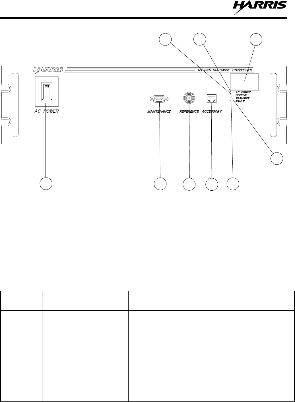
2.2 FRONT PANEL CONTROLS, INDICATORS, AND CONNECTORS
Figure 2-1 shows the controls, indicators, and connectors on the MX-9325 Transceiver front panel. Table 2-1
describes the controls, indicators, and connectors.
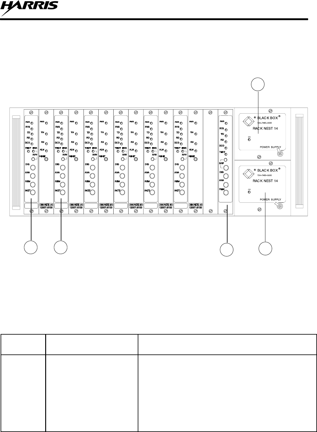
Figure 2-2 shows the controls and indicators on the VHF Extender Unit front panel. Table 2-2 describes the
controls and indicators.
MX-9325
OPERATION
2-2
Figure 2-1. Front Panel Controls, Indicators, and Connectors
FRONT VIEW
12345
6
78
9325-003
9
Table 2-1. Front Panel Controls, Indicators, and Connectors
Key
(Fig 2-1) Control/Indicator Function
1Power ON/OFF Switch Used to power MX-9325 Transceiver on or off.
2 Maintenance Port Used for local control and setup of transceiver.
3Frequency Reference Oscillator Test – used to measure and calibrate MX-9325 Transceiver ref-
erence oscillator.
4Accessory connector Used to test receive and transmit audio parameters in MSK
mode.
5Fault LED Lights when internal fault is detected.
6Transmit LED Lights when MX-9325 Transceiver is transmitting data.
7Receive LED Lights when MX-9325 Transceiver is receiving data.
8AC Power LED Lights when MX-9325 Transceiver is powered on.
9Product Identification Tag Contains MX-9325 Transceiver part number and serial number.
MX-9325
OPERATION
2-3
Figure 2-2. VHF Extender Unit 9325-004
9325–004
1 2 34
5
Table 2-2. VHF Extender Unit Controls, Indicators, and Connectors
Key
(Fig 2-2) Control/Indicator Function
1EIA-530 Modem High Speed Modem
PWR EIA-530 Modem - LED Lights Green when modem power is on.
RTS EIA-530 Modem – LED Lights Yellow when terminal (DTE) activates the
Request-to-Send line.
TD EIA-530 Modem - LED Lights Yellow when SPACE is being transmitted. Flickers as data
is transmitted.
RD EIA-530 Modem - LED Lights Yellow when steady SPACE is being received. Flickers as
data is received.
DCD EIA-530 Modem - LED Lights Yellow when a valid receive signal is present.

MX-9325
OPERATION
2-4
Table 2-2. VHF Extender Unit Controls, Indicators, and Connectors – Continued
Key
(Fig 2-2) Control/Indicator Function
TEST EIA-530 Modem - LED Lights Red when the modem is in any one of the three Loopback
modes - DIG, ANA, REM, or when the PATT pushbutton is
depressed.
ERR EIA-530 Modem - LED Lights Yellow momentarily when PATT switch is activated and
then goes out. If there are errors in the test pattern, the LED blinks
or remains lit.
RPF EIA-530 Modem - LED Lights when there’s a power failure in remote standalone unit.
May be reset by depressing the red RPT reset pushbutton.
DIG EIA-530 Modem - LED The Digital loopback switch causes the local modem to loop
received data and clock back to its transmitter. Data set ready will
turn off.
ANA EIA-530 Modem - Pushbutton The Analog Loopback switch causes the local modem to loop its
transmitter output back to its receiver. This Loopback may also be
activated from the DTE per V.54, Loop 3- Local Loopback, via
pin 18 on the EIA-530 D sub-connector interface.
REM EIA-530 Modem - Pushbutton
switch The Remote Signal Loopback switch causes the remoted EIA-530
modem to loop received data and clock to its transmitter. Data set
Ready will turn off. This loopback may be also activated from the
DTE per V.54, Loop 2 – Remote Loopback, via pin 21 on the
EIA-530 D sub-connector interface.
PATT EIA-530 Modem - Pushbutton
switch The pattern switch causes the EIA-530 modem to send and receive
a 511-bit test pattern. If errors are encountered by the receiver, the
ERR LED will light or flicker. The RD and CTS will turn off.
NOTE
The modem must be set to constant carrier, or if set to switched
carrier the RTS signal must be asserted (high) for the test to work.
RPF EIA-530 Modem - RESET
Pushbutton switch When pushed will reset the ERR LED.
2Discrete I/O Card
PWR Discrete I/O Card - LED Lights Green when Discrete I/O Card power is on.
TX Discrete I/O Card - LED Lights Yellow when transmit discrete line signal is asserted.
RX Discrete I/O Card - LED Lights Yellow when receive discrete line signal is asserted.
ALM Discrete I/O Card - LED Lights Red when circuit does not receive a valid signal for > 10 ms
RESET Discrete I/O Card - Pushbutton
switch When pushed, will reset the ALM LED.
3RS-232 Modem Low Speed Modem
RTS RS-232 Modem - LED Lights Green when RS-232 power is on.
PWR RS-232 Modem - LED Lights Yellow when terminal (DTE) activates the
Request-to-Send line.
TD RS-232 Modem - LED Lights Yellow when SPACE is being transmitted. Flickers as data
is transmitted.
RD RS-232 Modem - LED Lights Yellow when SPACE is being received. Flickers as data is
received.
DCD RS-232 Modem - LED Lights Yellow when a valid receive signal is present.

MX-9325
OPERATION
2-5
Table 2-2. VHF Extender Unit Controls, Indicators, and Connectors – Continued
Key
(Fig 2-2) Control/Indicator Function
TEST RS-232 Modem- LED Lights Red when the modem is in any one of the three Loopbac k
modes DIG, ANA, or REM.
RPF RS-232 Modem - LED Lights Red and indicates power failure in remote standalone units.
May be reset by depressing the red RPT reset pushbutton.
DIG RS-232 Modem Pushbutton
Switch Digital Loopback Switch. When pushed, causes the local modem
to loop received data and clock back to its transmitter. Data set
ready will go low.
ANA RS-232 Modem - Pushbutton
Switch Analog loopback switch, when pushed will cause the local modem
to loop its transmitter output back to its receiver. This loopback
may also be activated from the DTE per V.54, Loop 3- Local
Loopback, via pin 18 on the RS-232 D sub-connector interface.
REM RS-232 Modem - Pushbutton
Switch Remote Digital Loopback Switch, when pushed will cause the
remote RS-232 modem to loop received data and clock to its
transmitter. Data Set Ready will go low. This loopback is also
activated from the DTE per V.54, Loop 2 – Remote Loopback, via
pin 21 on the RS-232 D sub-connector interface.
RPF RS-232 Modem - RESET
Pushbutton Switch. When pushed, will reset the RPF LED.
4Power Supply 115 Vac Power Supply
5Power Supply 230 Vac Power Supply
2.3 BASIC OPERATION
Before operating, the MX-9325 transceiver and VHF Extender Unit must be installed per Chapter 8 and
configured per Chapter 3. The following paragraphs provide basic operating procedures of the MX-9325
Transceiver and VHF Extender Unit.
2.3.1 Initial Settings and Power Up
Initial settings and power up consists of powering up the transmitter and running BIT. Table 2-3 provides the
initial settings and power up procedure.
NOTE
The <enter> following each command means that an ASCII CR
(carriage return) is sent to the transmitter microcontroller which
causes the command to be executed.

MX-9325
OPERATION
2-6
Table 2-3. Initial Settings and Power Up Procedure
Step Control Action Observe
1Transmitter rear panel
J104 Antenna Connector Connect Antenna or a 50-Ohm/100 W
RF Attenuator.
2POWER switch on the PC
or terminal. Place switch in the ON position. The PC boots or terminal
powers on.
Refer to the PC or terminal
operation instructions for
more information.
3If using a PC, run the desired terminal
emulation program. Refer to Chapter 3
Paragraph 3.2.1.
The PC runs the terminal
emulation program.
Refer to software operation
instructions for more
information.
4Ensure that the terminal or terminal
emulation program communication
parameters are correctly configured,
as described in Chapter 3, Paragraph
3.2.1.
Refer to software operation
instructions for more
information.
5POWER switch on the
transmitter. Place switch in the ON position. The front panel AC power
indicator LED lights and the
PC or terminal displays the
initial power up screen. See
Figure 2-1.
If the PC or terminal does not
display the initial power up
screen, refer to Chapter 5,
Paragraph 5.2.3.
6PC or terminal keyboard Type bit v <enter>.The transmitter executes all
BIT tests, then displays the
results on the PC or terminal.
If a BIT fault is detected, refer
to Chapter 5 Paragraph 5.2.2.
2.3.2 MX-9325 Transceiver Operation
The MX-9325 Transceiver is operated by means of a VGC. The transceiver’s rear panel mounted host port
provides the interface. The communications protocol is the LAPB, variant of the HDLC protocol. The VGC is
linked to the MX-9325 Transceiver rear panel HOST port for local operation or to the rear panel EXTENDER
port for remote or split site (two transceivers used as separate receiver and transmitter) operation via a VHF
extender unit. All operations are performed from the VGC using ACARS, Mode 2 and management software
packages. Refer to the VGC and software operations manual for operating information.
MX-9325
PROGRAMMING/SETUP
3-1
CHAPTER 3
PROGRAMMING/SETUP
3.1 INTRODUCTION
This chapter provides information required to setup and configure the MX-9325 Transceiver.
The MX-9325 Transceiver should be powered up and pass BIT fault isolation before setup or configuration
procedures are performed. Refer to Chapter 2.
3.2 SETUP
The following provides instructions on configuration and setup of the MX-9325 Transceiver. These are generally
performed once during installation.
Setup and configuration maintenance commands are performed locally using a PC or ASCII terminal attached to
the MX-9325 Transceiver front panel mounted maintenance port.
WARNING
Voltages hazardous to human life are present if Maintenance
commands are not performed properly. Failure to preform
Maintenance commands properly can cause Injury or death to
personnel.
CAUTION
Maintenance commands are intended for maintenance personnel
only. Failure to perform maintenance commands properly could
cause equipment damage.
The following paragraphs describe access levels, setup and configuration commands performed locally from
the MX-9325 Transceiver maintenance port.
3.2.1 Terminal Emulation Software Configuration
The PC running terminal emulation software or the terminal that is connected to the transmitter (rear panel J1
MAINTENANCE connector) must be configured as follows:
•19,200 baud rate
•8 data bits
•1 start bit
•1 stop bit
•No parity
Refer to the operation documentation supplied with the terminal or terminal emulation software for more
information.

MX-9325
PROGRAMMING/SETUP
3-2
NOTE
Ensure that the correct Comm. Port (i.e. Comm. 1) on the PC is
selected to correspond with the connection to the MX-9325
Transceiver J1 connector.
3.2.2 Access Levels
The MX-9325 Transceiver can be accessed at the following levels:
•Monitor Level
•Maintenance Level
•Off-line Level
In Monitor level, the maintenance port user can view various radio operational and configuration parameters.
In Maintenance level, the maintenance port user can modify various operational and configuration parameters. All
host computers connected through the host port are prohibited from changing any operational and configuration
parameters until the maintenance port returns to monitor access. The host port will continue the ability to transmit
and receive data in the access level.
In Off–line level, the maintenance port user has the same restrictions as when the user has maintenance level
access. In addition, the radio cannot accept data from the host for transmission, and cannot forward to the host
port any data that is received off-the-air.
3.2.3 Changing Access Levels
The following paragraphs describe how to change the MX-9325 Transceiver access levels.
3.2.3.1 Monitor Level
To place the MX-9325 Transceiver into Monitor Level, type the following command on the PC/Terminal:
PWD <enter>
3.2.3.2 Maintenance Level
To place the MX-9325 Transceiver into Maintenance Level, type the following command on the PC/Terminal:
PWD Maintenance <enter>
3.2.3.3 Off-line Level
To place the MX-9325 Transceiver into Offline Level, type the following command on the PC/Terminal:
PWD No RF <enter>
3.2.4 Configuration Index
Table 3-1 lists the configuration index for the MX-9325 Transceiver. Column 1 contains the command as would
be typed on the PC/Terminal. Column 2 contains the brief descriptions of the command. Columns 3, 4 and 5
contain the access level the command can be performed at. Column 6 contains a reference to the paragraph that
describes the command in detail.

MX-9325
PROGRAMMING/SETUP
3-3
Table 3-1. MX-9325 Transceiver Configuration Index
Command Operation Procedure Monitor Maintenance Off-
line Para-
graph
BIT Display BIT results. 3.2.4.1
FRQ Display/Modify the current radio operating
frequency. 3.2.4.2
HIS Display a history of PBIT and CBIT faults
that have occurred since the last time the
historical BIT status word was cleared.
3.2.4.3
HWV Display the revision of each assembly in the
MX-9325 Transceiver. 3.2.4.4
PSU Display radio power supply voltages. 3.2.4.5
PWD Change current access level. 3.2.4.6
PWR Display/Modify the current transmitter
output power level. 3.2.4.7
STA Display the radio operational status. 3.2.4.8
SWR Display the Voltage Standing Wave Ratio
measured during the last transmission. 3.2.4.9
TMP Display the power amplifier and power sup-
ply heatsink temperatures. 3.2.4.10
VER Display the version identifiers of the active
and back-up software images currently
resident in the radio.
3.2.4.11
FPW Display the forward power level of the last
transmission. n n n 3.2.4.12
DBT Display the detailed BIT results for each
assembly in the radio. 3.2.4.13
KEY Display/Modify the current transmitter key
state. 3.2.4.14
MDL Display/Modify the modulation level set
point. 3.2.4.15
RPW Display the reverse power level of the last
transmission. 3.2.4.16
TCO Display/Modify the TCXO adjustment
value. 3.2.4.17
TIM Display/Modify transmitter continuous key
time-out interval. 3.2.4.18
SYC Display/Modify radio system
configuration. 3.2.4.19
MOD Display/Modify current operating mode. 3.2.4.20
TTO Generate a test tone. 3.2.4.21
MPS Display/Modify the local maintenance port
baud rate and parity settings. 3.2.4.22
DPS Display/Modify the host data port baud rate
setting. 3.2.4.23

MX-9325
PROGRAMMING/SETUP
3-4
Table 3-1. MX-9325 Transceiver Configuration Index – Continued
Command Operation Procedure Monitor Maintenance Off-line Para-
graph
RST Reset the radio. 3.2.4.24
CLF Clear the BIT fault word and detailed BIT
fault words for all assemblies. 3.2.4.25
CLH Clear the historical BIT status word. 3.2.4.26
SEN Run the receiver sensitivity test. 3.2.4.27
ACC Display/Modify the Mode 2 maximum
number of channel access attempts
parameter value.
3.2.4.28
ADL Display/Modify Mode 2 link level address. 3.2.4.29
PER Display/Modify the Mode 2 persistence
numerator parameter value. 3.2.4.30
TM1 Display/Modify the Mode 2 inter-access
delay timer parameter value. 3.2.4.31
TM2 Display/Modify the Mode 2 channel busy
timer time-out parameter. 3.2.4.32
CBT Display/Modify the ACARS channel busy
time-out parameter value. 3.2.4.33
UPF Display/Modify uplink filtering enable/
disable state.
3.2.4.34
DNF Display/Modify downlink filtering enable/
disable state. 3.2.4.35
RSF Display/Modify RSSI filtering enable/
disable state. 3.2.4.36
RFT Display/Modify RSSI filtering threshold
value. 3.2.4.37
ACS Display ACARS or Mode 2 statistics,
depending on current mode. 3.2.4.38
CBF Display/Modify Category B mode filter
character. 3.2.4.39
SER Display/Modify the radio serial number. 3.2.4.40
LPB Display/Modify the LAP-B parameters. 3.2.4.41
OVN Display the number of overruns. 3.2.4.42
OVZ Display the number of overruns and reset
the number to zero. 3.2.4.43
PRG Purge the messages and display the
number that were purged. 3.2.4.44
ELP Display/Modify the print software error
log enabled/disabled flag. 3.2.4.45
ERR Display the software error log. 3.2.4.46
HELP Display the commands available at the
current access level. 3.2.4.47
TVLS Display the Tx VCO lock state. 3.2.4.48

MX-9325
PROGRAMMING/SETUP
3-5
Table 3-1. Transmitter Operation Index – Continued
Command Operation Procedure Monitor Maintenance Offline Para-
graph
RVLS Display the Rx VCO lock state. n n n 3.2.4.49
BFLS Display the BFO PLL lock state. 3.2.4.50
LOLS Display the LO PLL lock state. 3.2.4.51
3.2.4.1 BIT – Display Current BIT Results
Display the current BIT fault code in hexadecimal format using the bit<enter> command. Refer to Chapter 5,
Paragraph 5.2.2 for a list of all BIT fault codes.
3.2.4.2 FRQ – Display or Modify the Current Radio Operating Frequency
Entering the command frq<enter> displays the current frequency in Hz.
Entering the command frq followed by a <space> and a valid frequency value in Megahertz will change the
MX-9325 Transceiver operating frequency to the specified value.
If an attempt to change the operating frequency to a value less than 118.000 or greater than 136.975, the
MX-9325 Transceiver rejects the command by displaying an error indication on the PC/Terminal, and no change
will be made to the operating frequency.
3.2.4.3 HIS – Display a History of BIT Fault Codes
Display a history of BIT fault codes using that have occurred since the last time the BIT status word was cleared
using his<enter>.
3.2.4.4 HWV - Display the Revision of each Assembly in the MX-9325 Transceiver
Display the character string containing the revision identifiers of each assembly in the MX-9325 Transceiver
using hwv<enter>. The revision identifiers will be displayed in the following order:
•Digital Processor Board: 12NNN-NNNN-NNX
•Receiver Board: 12NNN-NNNN-NNX
•Exciter Board: 12NNN-NNNN-NNX
•Directional Coupler: 12NNN-NNNN-NNX
•Power Amplifier: 12NNN-NNNN-NNX
•High Voltage Power Supply: 12NNN-NNNN-NNX
•Low Voltage Power Supply: 12NNN-NNNN-NNX
3.2.4.5 PSU – Display MX-9325 Transceiver Power Supply Voltages
Display MX-9325 Transceiver power supply voltages using psu<enter>. MX-9325 Transceiver voltages will be
displayed in tenths of a volt, for example +5V: 4.9. If any of the power supply voltages are not present in the
MX-9325 Transceiver, the corresponding value is displayed as 0 V.
3.2.4.6 PWD – Change Current Access Level
Entering the pwd command, followed by the correct level password to access to the Maintenance levels. Refer to
Paragraph 3.2.3 correct password.

MX-9325
PROGRAMMING/SETUP
3-6
3.2.4.7 PWR – Display or Change the Current MX-9325 Transceiver Output Power Level
Display the current MX-9325 Transceiver output power level using pwr<enter> command.
Change the MX-9325 Transceiver output power level using pwr followed by the new value in tenths of a watt.
For example, to change the MX-9325 Transceiver to a power output of 15 watts, type pwr 15.0<enter>.
3.2.4.8 STA – Display the Radio Operational Status
Entering the command sta<enter> displays the MX-9325 Transceiver operational status word in a hexadecimal
format.
3.2.4.9 SWR – Displays Voltage Standing Wave Ratio Measured During the Last Transmission
Display the most recently calculated SWR value using swr<enter>. The MX-9325 Transceiver displays with a
resolution of +/–.1.
3.2.4.10 TMP – Display the Power Amplifier and Power Supply Heatsink Temperatures
Display the current power supply and power amplifier heatsink temperatures using tmp<enter> command. The
temperatures displays with a resolution of +/–.1 degrees Celsius.
3.2.4.11 VER – Display Active and back-up Software versions
Display the active and back-up software versions stored in the MX-9325 Transceiver memory using ver<enter>.
3.2.4.12 FPW – Display the Forward Power Level
Display the MX-9325 Transceiver forward power level of the last transmission using fpw<enter>.
3.2.4.13 DBT – Display BIT Results for Each Assembly
Display the MX-9325 Transceiver detailed BIT results for each assembly using dbt<enter>.
3.2.4.14 KEY – Display or Change the Current Transmitter Key State
Entering the command key<enter> displays the MX-9325 Transceiver’s current transmitter key state as either
“ON” or “OFF.”
Entering the command key followed by a space and either the word “ON” or “OFF” will cause the MX-9325
Transceiver to key or unkey.
3.2.4.15 MDL – Display or Change Modulation Level Set Point
Display the current modulation level set point using the command mdl<enter>.
Entering the command mdl followed by a space and a valid modulation present value in decimal will change
the MX-9325 Transceiver modulation level set point.
3.2.4.16 RPW - Display the Reverse Power Level of the Last Transmission
Display the most recently measured reverse power level using the command rpw<enter>.
3.2.4.17 TCO - Display or Modify the TCXO Adjustment Value
Display the current MX-9325 Transceivers current TCXO adjustment value using the command tco<enter>.
Entering the command tco followed by a space and either + or – will change the TCXO adjustment value to up
one step or down one step, respectively.

MX-9325
PROGRAMMING/SETUP
3-7
3.2.4.18 TIM - Display or Modify Transmitter Continuous Key Time-out Interval
This is the maximum number of seconds the transmitter may be keyed continuously before it will automatically
unkey.
Display the maximum number of seconds of the transmitter continuous key time-out interval using the command
tim<enter>.
Entering the command tim followed by a space and a valid time-out value in seconds will change the continuous
key time-out interval.
3.2.4.19 SYC - Display or Modify Radio System Configuration
This defines how the radio is installed and what role it is to play in the communications system it is a part of. The
first command parameter defines what type of radio (MX-9325 Transceiver, transmitter, or receiver) the radio will
operate as. The second command parameter defines whether the radio talks to the host computer directly through
the host data port (Local), or whether it talks to a host computer or another radio via an extender unit through the
extender port (Remote). For a radio acting as a transmitter or receiver, it also defines whether the radio is installed
as a master radio in a split site configuration, and will be communicating with a remote radio as well as with a
host computer.
NOTE
Changing the radio system configuration will cause the radio
to reboot.
Display the radio system configuration using the syc<enter> command.
The configuration will be displayed in two parts. The first part as either XC, TX or RX to indicate that the radio is
acting as a MX-9325 Transceiver, transmitter, or receiver, respectively. The second part as either LOC, MAS or
REM to indicate whether the radio is operating in standalone local, split site master, or remote mode, respectively.
Entering the command syc followed by a space and either the word XC, TX or RX followed by a space and either
the word LOC, MAS or REM causes the radio to set it’s system configuration according to the specified
combination.
3.2.4.20 MOD – Display or Modify Current Operating Mode
Display the MX-9325 Transceiver operating mode using the mod<enter> command.
Entering the command mod followed by a space and either the word “ACARS” or “M2” will change the
MX-9325 Transceiver operating mode to ACARS or MODE 2.
3.2.4.21 TTO – Generate a Test Tone
Internally generate a 1200 Hz test tone, a 2400 Hz test tone, a random sequence of 1200 Hz and 2400 Hz test
tones, or a 1 kHz test tone while the transmitter is keyed.
Entering the command tto followed by a space and either the word 1000, 1200, 2400 or RAND causes the
MX-9325 Transceiver to continuously transmit a 1000 Hz, 1200 Hz, 2400 Hz, or a random sequence of 1200 Hz
and 2400 Hz tones, respectively.
Entering the command tto followed by a space and the word OFF causes the MX-9325 Transceiver to terminate
any test tone generation and transmission currently taking place. Upon receiving a valid “TTO” command and
parameter, the radio displays the action being taken on the PC/Terminal.

MX-9325
PROGRAMMING/SETUP
3-8
3.2.4.22 MPS – Display or Modify the Maintenance Port Baud Rate and Parity Settings
Display the current Maintenance Port baud rate and parity settings using the command mps<enter>.
The radio displays the maintenance port configuration in two parts: the first part as a numerical value to indicate
maintenance port baud rate, and the second part as either O, E, or N to indicate that the maintenance port is set for
Odd, Even, or No parity, respectively.
Entering the command mps followed by a space and a numerical value for the desired baud rate, followed by a
space and either the character O, E, or N shall cause the radio to set its maintenance port baud rate and parity
setting to the specified values.
3.2.4.23 DSP – Display or Modify the Host Data Port Baud Rate Setting
Display the current Host Data Port baud rate setting using dsp<enter> command.
Entering the command dsp followed by a space and a numerical value for the desired baud rate, shall cause the
radio to set it’s host data port baud rate to the specified value.
3.2.4.24 RST – Reset the Radio
Entering the command rst<enter> causes the radio to reset and go through its power-up initialization sequence.
3.2.4.25 CLF – Clear the BIT Fault Word and Detailed BIT Fault Words for all Assemblies
Entering the command clf<enter> causes the radio to clear all current faults by resetting all bits in the BIT fault
word and in the detailed BIT fault words for each assembly.
3.2.4.26 CLH – Clear Historical BIT Status Word
Entering the command clh<enter> causes the radio to clear the fault history by resetting all bits in the historical
BIT status word.
3.2.4.27 SEN – Run Receiver Sensitivity Test
Entering the command sen<enter> causes the radio to run the receiver sensitivity test.
3.2.4.28 ACC – Display or Modify Mode 2 Maximum Number of Channel Access Attempts
Parameter Value
Display the radio Mode 2 maximum number of channel access attempts parameter value using the acc<enter>
command.
Entering the command acc followed by a space and a numerical value for the desired Mode 2 maximum
number of channel access attempts, causes the radio to set the maximum number of channel access attempts
parameter to the specified value.
3.2.4.29 ADL – Display or Modify Mode 2 Link Level Address List
Display the current link level address list, or an indication that the list is empty if there are no addresses in the list
using the command adl<enter>.
Entering the command adl followed by a space and a value representing an address to be added to the list, causes
the radio to add the specified value to the address list. If a user attempts to add an address and the list already
contains four addresses, the radio will reject the command by displaying an error indication on the PC/Terminal,
and no change will be to the link level address list.
Entering the command adl followed by a character ‘c’ causes the radio to delete all addresses currently in the list
and indicate on the PC/Terminal that the list is now empty.

MX-9325
PROGRAMMING/SETUP
3-9
3.2.4.30 PER – Display or Modify the Mode 2 Persistence Numerator Parameter Value
Display the Mode 2 persistence numerator parameter value using the per<enter> command.
Entering the command per followed by a space and a numerical value for the persistence numerator value,
causes the radio to set the Mode 2 persistence numerator parameter to the specified value. If changing the Mode 2
persistence numerator parameter outside the range 0 to 255 (inclusive), the radio rejects the command by
displaying an error indication on the PC/Terminal, and no change will be made to the persistence numerator
parameter.
3.2.4.31 TM1 – Display or Modify the Mode 2 Inter-Access Delay Timer Parameter Value
Display the Mode 2 inter-access delay timer parameter in half-milliseconds using the tm1<enter> command.
Entering the command tm1 followed by a space and a numerical value for the desired Mode 2 inter-access
delay timer in half-milliseconds, causes the radio to set the inter-access delay timer parameter to the specified
value. Changing the Mode 2 inter-access delay timer outside the range 1 to 250 (inclusive), the radio rejects the
command by displaying an error indication on the PC/Terminal, and no change will be made to the inter-access
delay timer parameter.
3.2.4.32 TM2 – Display or Modify the Mode 2 Channel Busy Timer Time-out Parameter Value
Display the Mode 2 channel busy timer time-out parameter in seconds using the tm2<enter> command.
Entering the command tm2 followed by a space and a numerical value for the desired Mode 2 channel busy
timer time-out value in seconds, causes the radio to set the channel busy timer time-out parameter to the
specified value. Changing the Mode 2 channel busy timer time-out outside the range 6 to 120 (inclusive), the
radio rejects the command by displaying an error indication on the maintenance port terminal, and no change will
be made to the channel busy timer time-out parameter.
3.2.4.33 CBT – Display or Modify the ACARS Channel Busy Time-out Parameter Value
Display the ACARS channel busy time-out parameter in seconds using the cbt<enter> command.
Entering the command cbt followed by a space and a numerical value for the desired ACARS channel busy
time-out value in seconds, causes the radio to set the ACARS channel busy time-out parameter to the specified
value. Changing the ACARS channel busy time-out outside the range 6 to 120 (inclusive), the radio rejects the
command by displaying an error indication on the PC/Terminal, and no change will be made to the channel busy
time-out parameter.
3.2.4.34 UPF – Display or Modify Uplink Filtering Enable/Disable State
Display the current uplink filtering state as either “ON” or “OFF” using the upf<enter> command.
Entering the command upf followed by a space and either the word “ON” or “OFF” causes the radio to enable or
disable uplink filtering, respectively.
3.2.4.35 DNF – Display or Modify Downlink Filtering Enable/Disable State
Display the current downlink filtering state as either “ON” or “OFF“ using the dnf<enter> command.
Entering the command dnf followed by a space and either the word “ON” or “OFF” causes the radio to enable or
disable downlink filtering, respectively.

MX-9325
PROGRAMMING/SETUP
3-10
3.2.4.36 RSF – Display or Modify RSSI Filtering Enable/Disable State
Display the current RSSI filtering state as either “ON” or “OFF” using the rsf<enter> command.
Entering the command rsf followed by a space and either the word “ON” or “OFF” causes the radio to enable or
disable RSSI filtering, respectively.
3.2.4.37 RFT – Display or Modify RSSI Filtering Threshold Value
Display the RSSI filtering threshold parameter value using the rft<enter> command.
Entering the command rft followed by a space and a numerical value for the RSSI filtering threshold value,
causes the radio to set the RSSI filtering threshold parameter to the specified value. Changing the RSSI filtering
threshold parameter outside the range 0 to 100 (inclusive), the radio rejects the command by displaying an error
indication on the PC/Terminal, and no change will be made to the RSSI filtering threshold parameter.
3.2.4.38 ACS - Display ACARS or Mode 2 Statistics
Display the most recently calculated S1 and S2 statistic values when in ACARS using the acs<enter> command.
Display the most recently calculated S3 and S4 statistic values when in Mode 2 using the acs<enter> command.
3.2.4.39 CBF – Display or Modify Category B Mode Filter Character
Display the current Category B mode filter character using the cbf<enter> command.
Entering the command cbf followed by a space followed by a valid Category B mode filter character, causes
the radio to change Category B mode filter character to the specified character.
3.2.4.40 SER – Display the Radio Serial Number
Display the MX-9325 Transceiver serial number using the ser<enter> command.
3.2.4.41 LPB – Display or Modify the LAP-B Parameters
Display the Host Port LAP-B parameter values using the lpb<enter> command.
Entering the command lpb followed by a space and a numerical value for each of the window size, t1, t2, t4,
and n2 values, causes the radio to set the LAP-B parameters to the specified values.
3.2.4.42 OVN – Display the Number of Overruns
Display the number of overruns using the ovn<enter> command.
3.2.4.43 OVZ – Display the Number of Overruns and Reset the Number to Zero
Display the number of overruns and reset the number to zero using the ovz<enter> command.
3.2.4.44 PRG – Purge the Messages and Display the Number of Purged Messages
Purge messages and display the number of messages that have been purged using the ovz<enter> command.
3.2.4.45 ELP – Display or Modify the Print Software Error Log enabled/disabled Flag
Display the current print software error log state as either “ON” or “OFF” using the elp<enter> command.
Entering the command elp followed by a space and either the word “ON” or “OFF” causes the radio to change
the current print software error log state.
3.2.4.46 ERR – Display the Software Error Log
Display the current software error log using the err<enter> command.

MX-9325
PROGRAMMING/SETUP
3-11
3.2.4.47 HELP – Display the Commands Available at the Current Access Level
Display the commands that are valid at the current access level using the help<enter> command.
3.2.4.48 TVLS – Display the Tx VCO Lock State
Display the Tx VCO lock state using the tvls<enter> command.
3.2.4.49 RVLS – Display the Rx VCO Lock State
Display the Rx VCO lock state using the rvls<enter> command.
3.2.4.50 BFLS – Display the BFO PLL Lock State
Display the BFO PLL lock state using the bfls<enter> command.
3.2.4.51 LOLS – Display the LO PLL Lock State
Display the LO PLL lock state using the lols<enter> command.

MX-9325
PROGRAMMING/SETUP
3-12
This page intentionally left blank.

MX-9325
FUNCTIONAL DESCRIPTION
4-1
CHAPTER 4
FUNCTIONAL DESCRIPTION
4.1 INTRODUCTION
This chapter covers the functional description of the circuitry in the transceiver. Paragraph 4.2 provides a
simplified functional description and Paragraph 4.4 provides a detailed transceiver functional description.
Paragraph 4.3 provides a detailed extender unit functional description. Refer to Chapter 5 for BIT and
troubleshooting information. For parts list and family tree information, refer to Chapter 7, Paragraph 7.4. Refer to
Appendix A for the glossary of terms.
4.2 SIMPLIFIED TRANSCEIVER FUNCTIONAL DESCRIPTION
See Figure 4-1. The transceiver contains J1 Host Port for computer interface, digital processor and MSK/D8
modem function, receiver function, Transmitter function, power amplifier, and low pass filter/directional coupler.
It operates as a DSB AM MSK data transceiver and a digital data transceiver. As an AM MSK DSB data
transceiver, the radio operates according to the ACARS specifications. The transceiver contains an internal MSK
modem function providing all modulation/demodulation and CSMA for media access control. As a digital data
transceiver, the radio operates in Mode 2 (31.5 kbit per second suppressed carrier Differential 8 Phase Shift Key
modulation, CSMA.
4.3 SIMPLIFIED VHF EXTENDER UNIT FUNCTIONAL DESCRIPTION
See Figure 4-2. The VHF Extender Unit contains a EIA-530 Modem and a discrete I/O card required for remote
and split site system configurations. A RS-232 Modem is used with an optional Antenna Relay Switch installed.
The Discrete I/O card extends the receiver’s channel busy and the transceiver’s receiver mute differential signal
output lines for transceiver operation in split site ACARS and Mode 2. Signal interfaces are extended to the
remote site by means of a current loop interface circuit, capable of driving the required maximum length of hard
wire lines between sites.
The EIA-530 modem interface is used in the VHF Extender Unit to support the extension of computer to the
remote transceiver rear panel host port, or the from a local transceiver to a remote transceiver in split site
configuration. The Modem accommodates a variety of digital data interfaces: V.24/RS-232, V/35, X.21, EIA-530,
V.36 (RS-449), G.703 and Ethernet.
The EIA-530 modem features V.54 diagnostic capabilities to perform local analog loopback and local and remote
digital loopback. The loops can be manually activated from the front panel or via control signals from the
interface connector. In addition, the EIA-530 modem incorporates a built-in BERT to enable complete testing of
both modems and the intersite line. A front panel switch generates a pseudo-random test pattern (511 bits)
according to ITU V.52, for testing end-to-end connectivity. An ERROR LED located on the front or the modem,
flashes when a bit error is detected.
The modem’s range at a particular data rate is dependent on the transmission line wire gauge. At a data rate of 192
kbps, 22 AWG wire is sufficient for intersite lines up to 4.5 km in length. Intersite lines of 19 AWG wire are
required to support transmission at 192 kbps on lines greater than 4.5 km long. Table 4-1 lists the approximate
range of the EIA-530 modem over various gauges of unconditioned transmission line.
The RS-232 modem provides an RS-232D (EIA-232/V.24) digital data interface to the Computer. The RS–232
modem is selected for use in the Extender Units to support the extension of the Antenna Switch Serial Control
Port from the local computer to remote site Antenna Switches in Remote Site and Split Site configurations.
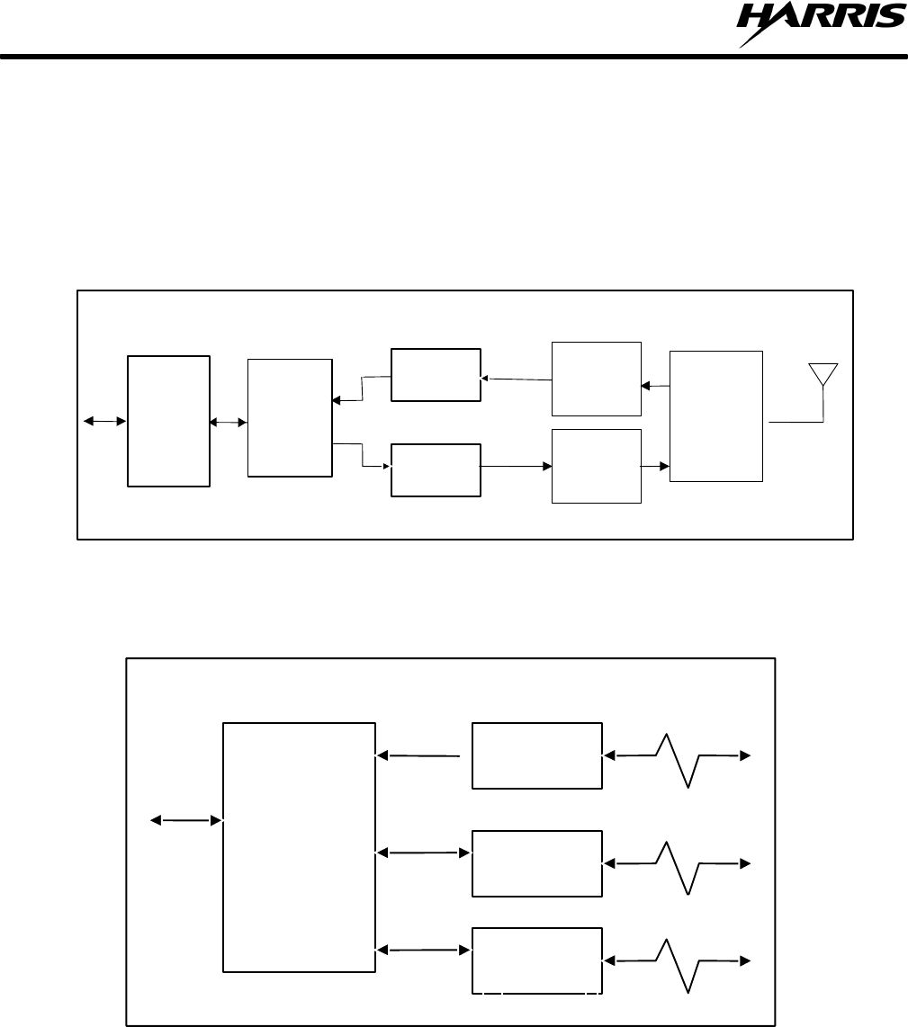
MX-9325
FUNCTIONAL DESCRIPTION
4-2
The modem’s range at a particular data rate is dependent on the transmission line wire gauge. At a maximum data
rate of 19.2 kbps, 26 AWG wire is sufficient for intersite lines up to 7.5 km in length. The RS–232 modem
features V.54 diagnostic capabilities to perform local analog loopback and local and remote digital loopback. The
loops can be manually activated from the front panel or via control signals from the interface connector. Table 4-2
lists the approximate range or the RS-232 Modem over various gauges of unconditional transmission lines.
Figure 4-1. Transceiver Simplified Block Diagram
9325-005
Ground
computer
Interface
Digital
Processor
&
MS K
Function
Filter
Power
Amp
Directional
coupler
Ground
computer
Interface
Transmitter
Function
Receiver
Function
Figure 4-2. Extender Unit Simplified Block Diagram 9325-006
Rear Panel
Interface
RS-232
Modem
(For ARS)
Discrete
I/O
EIA-530
Modem
5Km
5Km
5Km
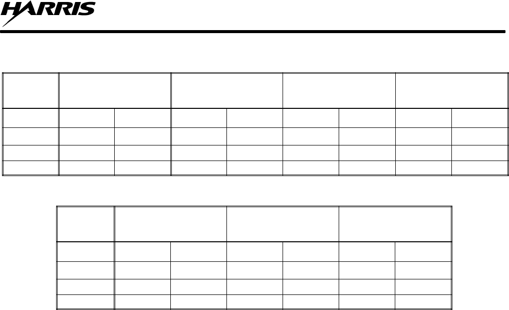
MX-9325
FUNCTIONAL DESCRIPTION
4-3
Table 4-1. EIA-530 Modem Approximate Maximum Range
DATA
RATE 19 AWG 22 AWG 24 AWG 26 AWG
km miles km miles km miles km miles
192 kbps 6.0 3.7 4.5 2.8 3.5 2.2 2.7 1.7
144 kbps 10.6 6.6 6.75 4.2 4.5 2.8 3.4 2.1
128 kbps 12.4 7.7 7.3 4.5 5.0 3.1 3.6 2.2
Table 4-2. RS-232 Modem Approximate Maximum Range
DATA
RATE 19 AWG 24 AWG 26 AWG
km miles km miles km miles
19.2 kbps 22.5 14 10 6.2 7.5 4.6
14.4 kbps 24.5 15.2 11 6.8 8.2 5.1
9.6 kbps 29 18 13 8 9.5 5.9
4.4 DETAILED TRANSCEIVER FUNCTIONAL DESCRIPTION
The following paragraphs provides detailed functional description of the transceiver. Paragraph 4.4.1 describes
the transceiver signal paths. Figures 4-3 through 4-7 shows the transceiver signal path block diagrams.
4.4.1 Transceiver Signal Paths
•Transmit/Receive Data Signal Paths – Paragraph 4.4.2
•Transmit RF Signal Paths - Paragraph 4.4.3
•Receive RF Signal Paths - Paragraph 4.4.4
•Control/Interface Signal Paths – Paragraph 4.4.5
•BIT Signal Path – Paragraph 4.4.6
•Power Distribution – Paragraph 4.4.7
4.4.2 Data/RF/IF Signal Paths
The following paragraphs describe the functions of each assembly as they relate to the transmit and receive signal
path through the transceiver.
See Figure 4-3. Data messages enter A1A2 Digital Board PWB Assembly via the rear panel host port, extender
port as LAPB Frames.
4.4.2.1 A1A2 Digital PWB Assembly
Data to be transmitted enters A1A2 Digital PWB Assembly Host or extender interface port. The interface port
performs level shifting and routes serial data to a Power PC860 microprocessor. The microprocessor performs all
required integrity checks then sends data to a DSP which processes the digital data signals. The digital data is then
sent to the DAC to be converted to baseband analog. The DAC routes a parallel analog In-phase and Quadrature

MX-9325
FUNCTIONAL DESCRIPTION
4-4
(I and Q) audio signal to the exciter interface on A1A2 Digital PWB Assembly where it is sent to A1A3 Exciter
PWB Assembly.
In receive mode, the received signal is sent to A1A2 Digital PWB Assembly where the analog baseband signal is
converted to digital. The A1A2 Digital PWB Assembly mounted DSP measures the RSSI and implements AGC
by controlling the receiver’s IF and RF gain. In split site configuration, the DSP monitors the RSSI as reported by
local receiver, via the VHF extender unit, interfaces to generate a channel busy signal. The channel busy signal
applies the algorithm to the DSP to determine the correct transmission time. The DSP accepts baseband I and Q
audio from the receiver’s demodulator section and digitally demodulates those signals to generate recovered data.
Upon successful receipt of a data burst, the DSP executes any FEC algorithms, if available, and provides the data
to the microprocessor. The microprocessor formats the data for delivery to the VGC via A1A2 Digital PWB host
or extender interface port.
4.4.3 Transmit RF Signal Path
See Figure 4-4. The following paragraphs describe the Transmit RF Signal path of the MX-9325 Transceiver.
4.4.3.1 A1A3 Exciter PWB Assembly
The A1A3 Exciter PWB Assembly produces a frequency synthesized RF output modulated signal. The I and Q
audio signals are amplified and sent to a Vector Modulator Circuit. The modulated RF is sent through a second
amplifier then attenuated before leaving A1A3 Exciter PWB Assembly and routed to A1A4A1 Power Amplifier
PWB.
4.4.3.2 A1A4A1 Power Amplifier Assembly
The A1A4A1 Power Amplifier Assembly consists of two amplifier stages which amplify the modulated RF
signals from A1A3 Exciter PWB Assembly to a level of 25 watts, nominal. The amplified RF signal is sent to
A1A5 Low Pass Filter and Directional Coupler PWB Assembly.
4.4.3.3 A1A6 Directional Coupler Assembly
The A1A5 Low Pass Filter and Directional Coupler Assembly contains a low pass filter and antenna switch. The
low pass filter provides the required amount of attenuation at harmonics of the transmitter frequency.
The directional coupler is located between the low pass filter and antenna switch, and monitors both forward and
reflected power on the antenna feedline. The antenna switch switches the antenna between the power amplifier
output and receiver RF input. It consists of a solid-state PIN diode switch using quarter-wave transmission lines to
provide isolation between the transmitter output and the receiver input.
4.4.4 Receiver RF Signal Path
See Figure 4-5. The following paragraphs describe the Receive RF Signal Path.
4.4.4.1 A1A5 Low Pass Filter and Directional Coupler Assembly
The transceiver receives RF messages via the J5 antenna port. RF is passed through A1A5 Low Pass Filter and
Directional Coupler Assembly and A1A8 Helical Filter Assembly before entering A1A7 Receiver PWB
Assembly.
4.4.4.2 A1A7 Receiver PWB Assembly
The A1A7 Receiver PWB Assembly utilizes frequency synthesized oscillators to down convert and demodulate
on channel signals to be sent to A1A2 Digital PWB Assembly. The received signal strength voltage is also sent to
A1A2 Digital PWB Assembly for processing.
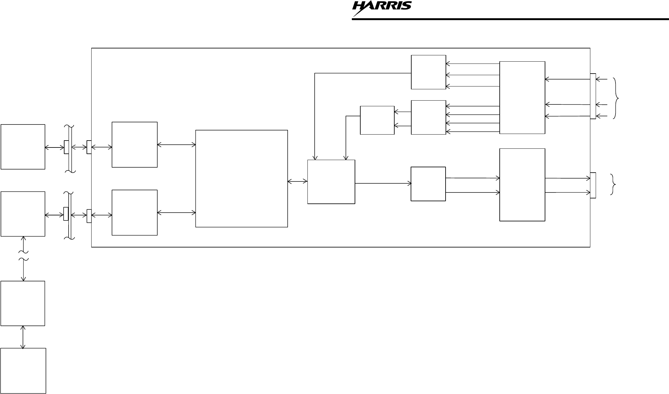
MX-9325
FUNCTIONAL DESCRIPTION
4-5/4-6
A4
Figure 4-3. Data/Transmit/Recieve
Signal Path Block Diagram
9325-007
I
Q
LOCAL
VGC
VHF
EXTENDER
UNIT
(MODEM)
HOST
INTERFACE
EXTENDER
INTERFACE
RSSI
POWER
PC860
MICROPROCESSOR
I
Q
EXCITER
INTERFACE
VHF
EXTENDER
UNIT
(MODEM)
I IN
AM_DEMOD
AM_DEMOD
DEMOD_DC
RF_RSSI
IF_AGC_CTRL
RX_Q
RX_I
RF_AGC_CTRL
Q IN
Q OUT
I OUT
REMOTE/SPLIT
SITE
VGC
TO
EXCITER
PWB
RECEIVER
INTERFACE
CODEC
2:1 MUX
DAC
P/O
J20
P/O
J12
FROM
RECEIVER
PWB
A/D
DSP
PART OF
REAR PANEL
PART OF
REAR PANEL
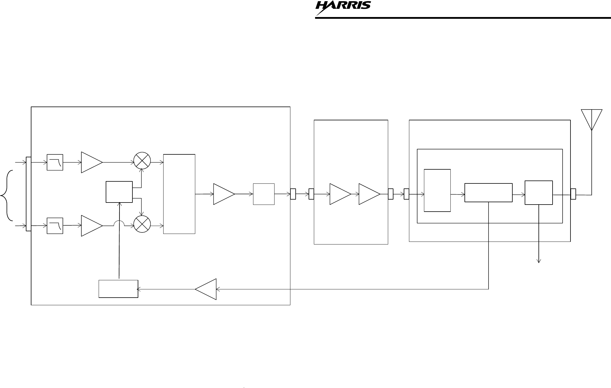
MX-9325
FUNCTIONAL DESCRIPTION
4-7/4-8
A4
Figure 4-4. Transmit RF Signal Path
Block Diagram
9325-008
FROM
DIGITAL
PWB
I CHANNEL
MIXER
I CHANNEL
DRIVER
I CHANNEL
FILTER
Q CHANNEL
FILTER Q CHANNEL
DRIVER
VARIABLE
ATTENUATOR
EXCITER
AMPLIFIER
QUAD
COUPLER RF
COMBINER
Q CHANNEL
MIXER
I IN
Q IN
II
I
QQ
Q
TO RECEIVER
CIRCUITS
OUTPUT
DRIVER
PRE
DRIVER
DIRECTIONAL COUPLER ASSEMBLY A5
POWER AMPLIFIER
ASSEMBLY
A1A4A1
FEEDBACK
AMPLIFIER
REFERENCE
OSCILLATOR
CIRCUIT
LOW
PASS
FILTER STRIPLINE
COUPLER ANTENNA
SWITCH
EXCITER PWB ASSEMBLY
J2 J1
P/O
J3
J5
J2 J1
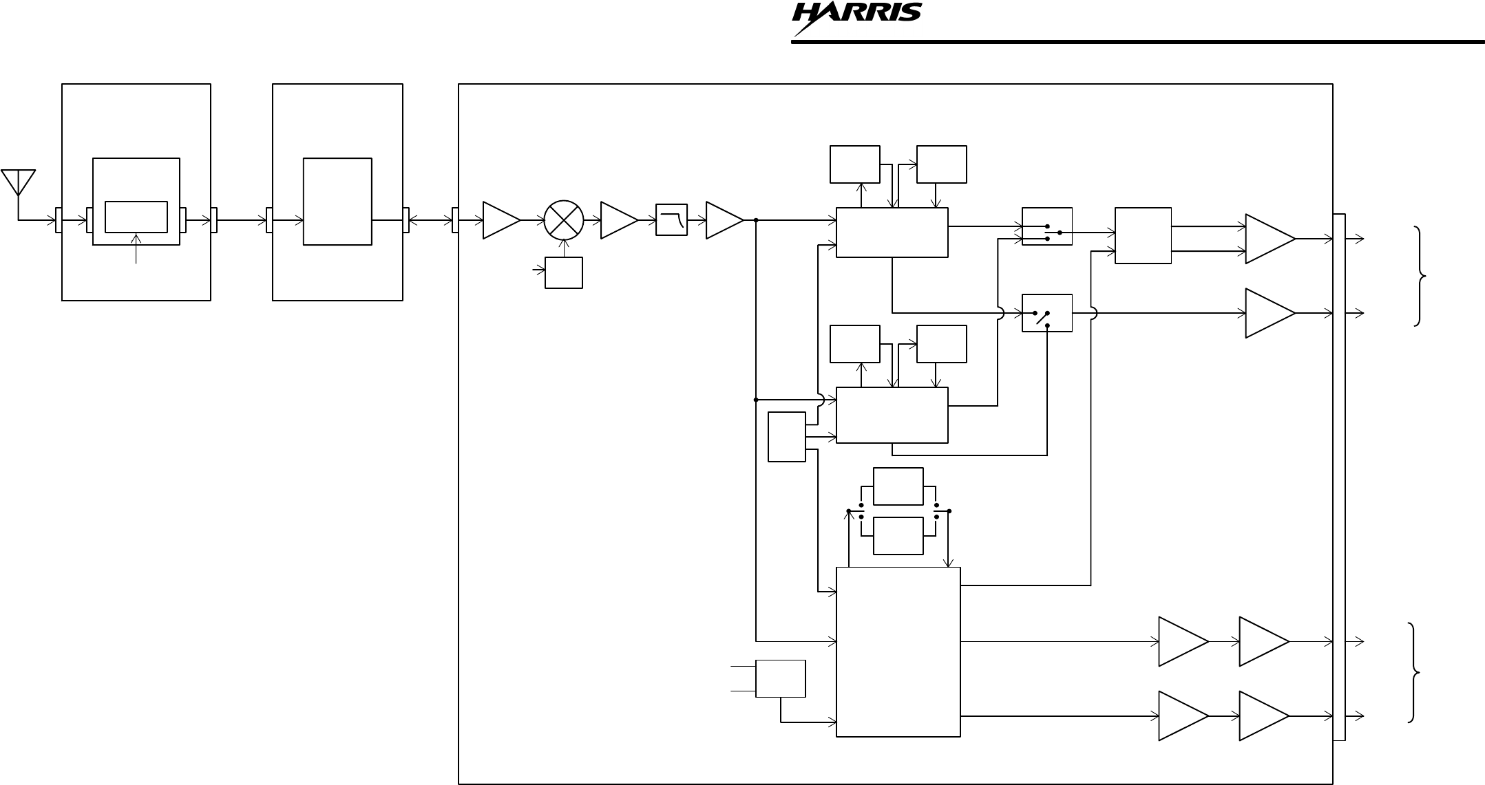
MX-9325
FUNCTIONAL DESCRIPTION
4-9/4-10
A4
Figure 4-5. Recieve RF Signal path
Block Diagram
9325-009
J5
DIRECTIONAL
COUPLER
ASSEMBLY
ANTENNA
SWITCH
FROM
TRANSMITTER
CIRCUITS
ANTENNA
PORT
HELICAL
FILTER
ASSEMBLY
RF PRE
AMPLIFIER MIXER
VCO
LO
REFERENCE
OSCILLATOR IN
1ST IF
AMPLIFIER
LOW
PASS
FILTER
2ND IF
AMPLIFIER
45 MHz IF
NARROW
BAND
FILTER
NARROW
BAND
FILTER
NARROW
BAND
MIXER/IF
WIDE
BAND
MIXER/IF
I
AMPLIFIER
I OUT
I PRE
AMPLIFIER
I
Q
AMPLIFIER
Q PRE
AMPLIFIER
QQ OUT
MIXER/
QUADRATURE
DETECTOR
I
Q
TO A1A2
DIGITAL PWB
ASSEMBLY
BFO_TV
BFO_ENABLE
BFO
NARROW
BAND
FILTER
WIDE
BAND
FILTER
WIDE
BAND
FILTER
WIDE
BAND
FILTER
SWITCH
RSI
AMPLIFIER
RF_RSI RSSI OUT
SWITCH
455 MHz IF
AM
DETECTOR
DEMOD_INV
DEMOD_NINV +
–AM_DEMOD
OUT
RSSI
LO
45 MHz IF
45 MHz IF
455 KHz
455 KHz
455 KHz IF
455 KHz IF
TO A1A2
DIGITAL PWB
ASSEMBLY
P/O A4 HEAT SINKS
J3 J1
A1A2 RECEIVER PWB ASSEMBLY
P/O J3

MX-9325
FUNCTIONAL DESCRIPTION
4-11
4.4.5 Control / Interface Signal Paths
See Figure 4-6. This figure illustrates the control paths that exist between the front panel maintenance port, front
panel LEDs, rear panel data port, DSP, exciter, receiver, power amplifier, and antenna. The control paths are
where the transceiver interacts with an external control terminal in the form of a PC or ASCII terminal. Since no
operator controls exist on the transceiver front panel, all control functions for the transceiver originate at the PC
or terminal. Control functions include parameter changes and readbacks, BIT and system status.
The following are descriptions of the various types of control that occur within the transceiver. The types of
control include the following:
•Front Panel Interface – Paragraph 4.4.5.1
•Internal A1A2 Digital PWB Assembly Functions – Paragraph 4.4.5.2
•A1A3 Exciter PWB Assembly – Paragraph 4.4.5.3
•Power Control Interfaces – Paragraph 4.4.5.4
•Receiver Control Interface– Paragraph 4.4.5.5
4.4.5.1 Front Panel Interface
Front panel interface consists of interfacing the maintenance port to A1A2 Digital PWB Assembly.
The PC or terminal is connected to the transceiver front panel mounted MAINTENANCE connector, an RS-232
port using a standard DB-9 serial connector. Data signals from the PC or terminal enter the transceiver through
this port and go directly to A1A2 Digital PWB Assembly. The control software is actually contained in a
EEPROM on A1A2 Digital PWB Assembly, allowing transceiver control via a dumb terminal. The control
software is accessed by the microcontroller on A1A2 Digital PWB Assembly, decoded, and used to initiate such
actions as frequency and bandwidth changes, self-test, and other parameter changes or readbacks. In addition, an
A1A2 Digital PWB Assembly mounted light-emitting diodes on the front panel indicate AC power, receive
carrier detector, transmit key status and fault.
4.4.5.2 Internal A1A2 Digital PWB Assembly
The A1A2 Digital PWB Assembly controls all functions in the transceiver and provides all interfaces to the rear
panel data port. A Flash EEPROM IC contains all software for the processors. At initialization, the
microprocessor fetches its operating software from the Flash EEPORM IC and copies it to its external DRAM IC
for execution. The microprocessor then initializes the DSP. The DSP operates exclusively from internal memory.
Factory programmed calibration data is fetched during power-on initialization. This data, as well as part number,
revision code, manufacturing date and serial number is stored in serially accessed EEPROM devices located on
each internal electrical subassembly. A single I2C bus interconnects these assemblies and the microprocessor. This
bus is inactive during normal operation of the transceiver.
Upon system reset, A1A2 Digital PWB Assembly configures all programmable parts of the system (synthesizers,
RDACs, etc) as required with data fetched from configuration memory. This memory consists of parameter
blocks in the EEPROM, updated when changes are commanded by the host or extender interface port. These
devices reside on a software controlled serial bus, which is not used after initialization is complete and remains
idle during normal transceiver operation.
During operation, A1A2 Digital PWB Assembly monitors certain diagnostic signals to determine if the
transceiver is still capable of operation within specifications. This process is known as BIT. Synthesizer lock
detect lines, heatsink temperature, antenna port match and regulated power supply voltages are examples of
monitored signals which, when out of tolerance, cause the unit to either reduce transmitter power level or create a

MX-9325
FUNCTIONAL DESCRIPTION
4-12
key inhibit condition. A multiplexed eight bit A/D converter connects to the microprocessor for most of the
analog BIT functions. The host port is notified of any change in BIT results.
The A1A2 Digital PWB Assembly is the source of the frequency reference for the other subassemblies in the
transceiver. A VCTCXO on A1A2 Digital PWB Assembly provides a 14.745 MHz signal which is stable to
within 1 ppm over the temperature range. The RDAC provides a means of accurately setting the oscillator
frequency and for compensating for crystal aging. The microprocessor controls the RDAC at initialization to fine
tune the output frequency. The RDAC value is determined during factory testing, and stored into the Flash
Memory IC parameter blocks.
4.4.5.3 A1A3 Exciter PWB Assembly
To perform the transmit function, A1A2 Digital PWB Assembly accepts data conforming to the interface
specification from the host port and performs all required integrity checks on the data. The A1A2 Digital PWB
Assembly enables circuitry on the exciter and power amplifier assemblies, and monitors the output of the dual
directional coupler in order to measure forward and reflected power. The output power level of the transmitter is
under control of A1A2 Digital PWB Assembly for ALC purposes. At the conclusion of the transmitted burst, it
disables the exciter and power amplifier until transmission is again required. The microprocessor monitors the
‘key confirm’ signal at all times to determine if a failure has enabled unauthorized transmission of RF energy.
4.4.5.4 Power Control Interfaces
The A1A2 Digital PWB Assembly individually controls A1A5 Low Pass Filter and Directional Coupler
Assembly mounted antenna switch, PA bias and driver bias and power control attenuator. These functions along
with the timing relationship between these signals and the exciter control signals for key up and down are
determined by the DSP.
Forward and reflected power samples are input to the DSP for power measurement. The DSP calculates the power
and SWR using calibration data stored on the directional coupler assembly and fetched by the microprocessor at
power up or reset. It controls the power output level, by changing the attenuation at the exciter level.
A digital signal, key confirm, is derived from the forward power sample and is input to the microprocessor. This
input is used to monitor the length of RF transmissions. If a transmission exceeds a fixed value, the
microprocessor unilaterally and permanently disables the transmit capability. Two mechanisms exist for disabling
transmissions: the microprocessor can disable the transmit VCO via a digital switch, and prevent the DSP from
biasing the power amplifier, via the power control interface described above.
The transceiver reports a Stuck Carrier condition on the RF channel when operating in either the ACARS mode or
Mode 2. In ACARS mode, a stuck carrier is declared when a carrier signal is detected for more than a configured
amount of time. Upon detecting the presence of a carrier for more than this configured time, the transceiver sends
an unsolicited response message to the computer via the host port indicating a stuck carrier condition. The
transceiver detects the absence of a stuck carrier signal and sends an unsolicited response message to the
computer indicating that a stuck carrier condition no longer exists.
In Mode 2, a stuck carrier condition is declared when the configured TM2 timer has expired. Upon the expiration
of the TM2 timer, the transceiver shall send an unsolicited response message to the computer indicating timer
TM2 has expired and a stuck carrier condition exists. The transceiver determines the absence of a stuck carrier
when successful access of the channel occurs. The transceiver sends an unsolicited response message to the
computer indicating that a stuck carrier condition no longer exists.
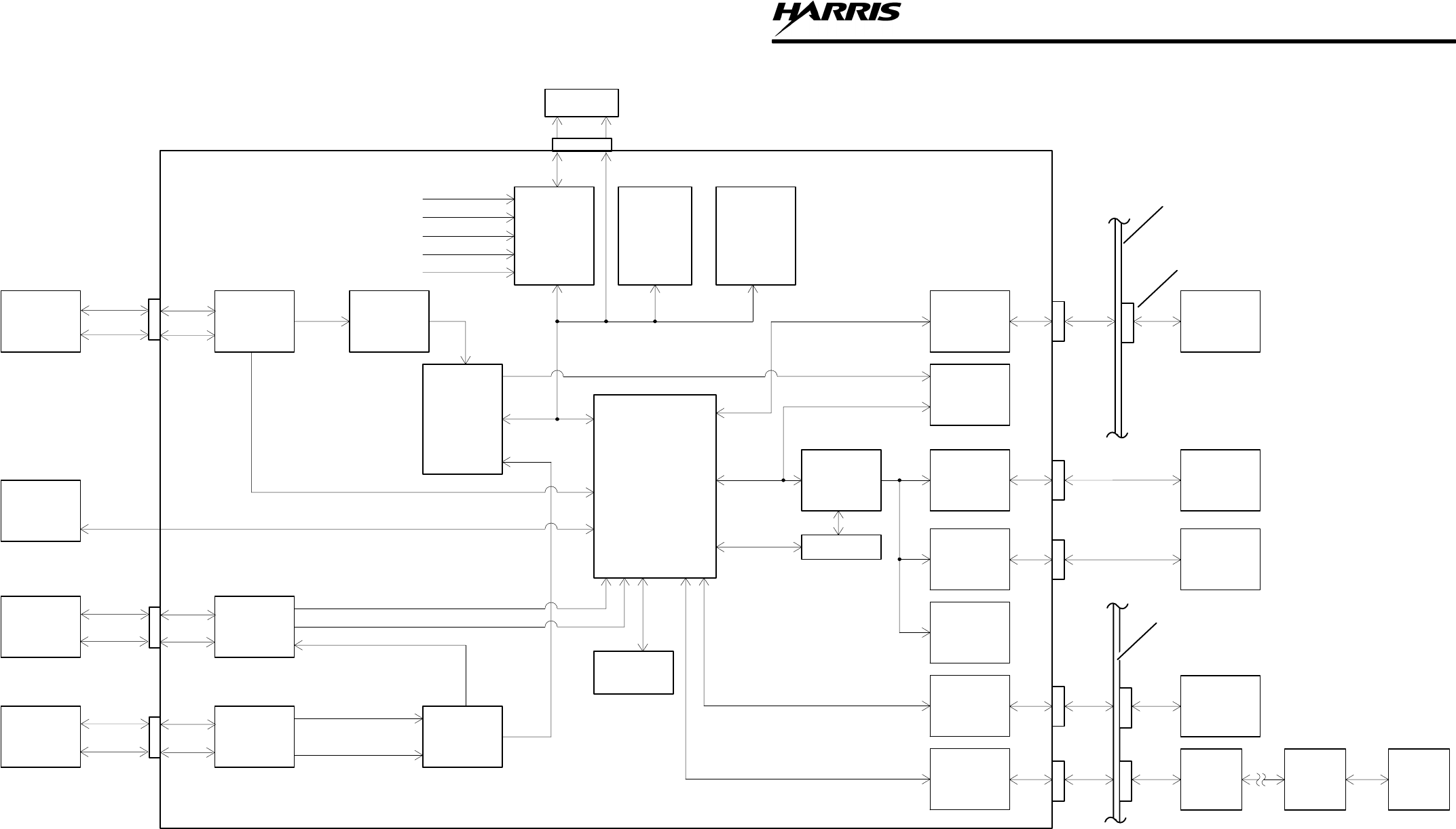
MX-9325
FUNCTIONAL DESCRIPTION
4-13/4-14
A4
Figure 4-6. Control Signal Path
Block Diagram
9325-010
RECEIVER
CIRCUITS
RF_RSSI
RECEIVER
INTERFACE CODEC
DSP
DIRECTIONAL
COUPLER
POWER
PC860
MICROPROCESSOR
CONFIGURATION
EEPROM
EXCITER
CIRCUITS
RF_RSSI
EXCITER
INTERFACE
CODEC
RX BIT SIGNALS
LOCK DETECT
TX BIT SIGNALS
PWR_CTRL
VSWR
PA
FWR_PWR
PA
INTERFACE
RVS_PWR
FWD_PWR
RVS_PWR
RS–232
MAINTENANCE
PORT
INTERFACE
FRONT
PANEL
LED
RECEIVER
REFERENCE
EXCITER
REFERENCE
FRONT
PANEL
REFERENCE
HOST PORT
INTERFACE
EXTENDER
PORT
INTERFACE
MAINTENANCE
PC / TERMINAL
RECEIVER
BOARD
EXCITER
BOARD
LOCAL VGC
EXTENDER
(MODEM)
EXTENDER
(MODEM)
REMOTE/
SPLIT SITE
VGC
VCTXO
REFERENCE
OSCILLATOR
RDAC
TEMP ADJ
RSSI
DC POWER
ADC FLASH
EEPROM IC DRAM IC
PS_TEMP
HS_TEMP
EXCITER_AMP
TX_OSC_AMP
SQL_CTL
DIGITAL PWB ASSEMBLY
P/O REAR PANEL
P/O REAR PANEL
FRONT PANEL
mAINTENANCE
PORT
J1
J12
J20
J3
J3
J1
J2
J16
J20
J12
J28

MX-9325
FUNCTIONAL DESCRIPTION
4-15
4.4.5.5 Receive Control Interface
The microprocessor programs the DDS and synthesizer loops with the common software controlled clock and
data outputs. Discrete, chip select outputs are provided for each serially programmed device and IF bandwidth
select and BFO enable outputs are provided to the receiver. The microprocessor monitors the three synthesizer
lock detect lines.
The DSP accepts an RSSI voltage supplied to an A/D converter, and uses D/A converters to control the IF gain
and RF attenuator stages for AGC. The bandwidth of the RSSI input is 10.5 kHz. Analog I&Q audio inputs to
matched A/D converters are used for D8PSK demodulation. A DC offset voltage for I&Q audio is provided for
level shifting purposes. For AM demodulation, the recovered AM signal and a DC voltage proportional to the
noise level of the signal is applied to A/D converters. The DSP is responsible for ALC and squelch functions.
4.4.6 MX-9325 Transceiver Built In Test (BIT)
See Figure 4-6. The transceiver executes internal diagnostic testing upon power up and under software command
to detect faults and ensure proper operation. BIT activates either remotely or locally via the front panel
maintenance interface port. The transceiver reports the results of BIT tests to the PC/Terminal upon operator
command either remotely or locally.
The extender unit provides internal diagnostic testing to ensure proper operation. Internal diagnostic testing is
applicable to transceivers and extender units in split site and remote site configurations. As part of BIT for split
site configuration, the local transceiver will control the loopback function of the transceivers and extender units.
The local transceiver reports separate BIT status to the computer via the host port for both the local and remote
transceivers.
BIT measures transmitter forward and reflected power in an online mode, as normal transmit traffic.
The transceiver reports to the computer via host port, a high VSWR condition in the BIT fault word response
whenever there is a change in the status.
BIT tests receiver sensitivity as part of the power up or initialization sequence. The transceiver has the capability
for a commanded receiver sensitivity test. The result of the receiver sensitivity test is reported in the BIT status
response.
Table 4-3 lists the BIT performed when the MX-9325 Transceiver is powered on. Refer to Chapter 3 for
information on performing a BIT command while the MX-9235 Transceiver is in operation. Refer to Chapter 5
for BIT fault code descriptions.
Table 4-3. MX-9325 Transceiver Power On BIT
BIT Test Failure Criteria
Memory test Read/write RAM test fail (critical fault), EEPROM test fail (Boot Fault).
Boot sequence Software image failed to load correctly.
DC voltage test Voltage out of tolerance.
EEPROM assembly checks Configuration information of EEPROM assemblies is invalid.
Synthesizers and oscillators out of
lock Oscillators failed to lock.
Power amplifier bias/RSSI check No power reading of RSSI.
Receiver sensitivity Sensitivity is too low.
Interprocessor communications test Communications with the VGC is lost.
RAM checks RAM verification checks failed.

MX-9325
FUNCTIONAL DESCRIPTION
4-16
4.4.7 MX-9325 Transceiver Power Distribution
See Figure 4-7. Power distribution consists of converting a 85 Vac to 265 Vac input to the various DC voltages
required by the transceiver assemblies, as discussed in the following paragraphs.
4.4.7.1 AC Line Voltage Path
85 Vac to 265 Vac enters the transceiver through rear panel mounted connector J1. The AC passes through a line
filter and the front panel mounted AC Power Switch (CB1) and goes to A1A4A2 28 Vdc Power Supply. The
A1A4A2 28 Vdc Power Supply takes the AC voltage and sends it to a power factor corrector module where it is
converted to 300 Vdc, then converted again to +28 Vdc. The +28 Vdc is sent to A1A6 Low Voltage Power Supply
where +5 Vdc, +15 Vdc, –15 Vdc and distributed along with +28 Vdc to the transceiver assemblies. A seperate
+28 Vdc is also sent directly to A1A4A1 Power Amplifier Assembly.
4.4.7.2 +28 Vdc Path
The +28 Vdc is routed to the following:
•A1A4A1 Power Amplifier Assembly via connector A1A4J1.
•A1A6 Low Voltage Power Supply via connector A1A4J2.
4.4.7.3 +5 Vdc, +15 Vdc, –15 Vdc and +28 Vdc Path
The +5Vdc, +15 Vdc, –15 Vdc and +28 Vdc is routed to the following:
•A1A2 Digital PWB Assembly via connector A1A6J4.
•A1A3 Exciter PWB Assembly via connector A1A6J6.
•A1A4A1 Power Amplifier Assembly via connector A1A6J2.
•A1A5 Low Pass Filter and Directional Coupler Assembly via connector A1A6J9.
•A1A7 Receiver PWB Assembly via connector A1A6J6
4.4.8 Software Download
The MX-9325 Transceiver maintains three non-volatile storage areas called Software Banks, to hold downloaded
software data. At any time, two of the banks are considered active and contain valid copies of the MX-9325
Transceiver operating software. This enables the radio to execute the most recent downloaded version of its
software, or to switch to a previously downloaded version via instruction from the VGC. The third bank is
regarded as inactive and is kept available as a receiving area for the next version to be downloaded. When a
MX-9325 Transceiver is shipped from the factory, it contains identical versions of software in all software banks,
although only two banks are regarded as containing active software versions.
The software download feature enables the host computer to update software in the MX-9325 Transceiver through
the host or Extender interface port. The MX-9325 Transceiver remains fully operational during the software
download process. software for all of the various processors inside the MX-9325 Transceiver are sent to the radio
bundled as one large package of binary data. Software downloads are stored by the radio into a volatile buffer
until the MX-9325 Transceiver has received all of the data and the data’s integrity has been verified.
4.4.9 VHF Extender Unit
The following paragraphs describe the data and control signal paths of the VHF Extender Unit circuit cards. For
additional information on the VHF Extender Unit and Modem Cards, refer to Chapter 1 Paragraph 1.5.
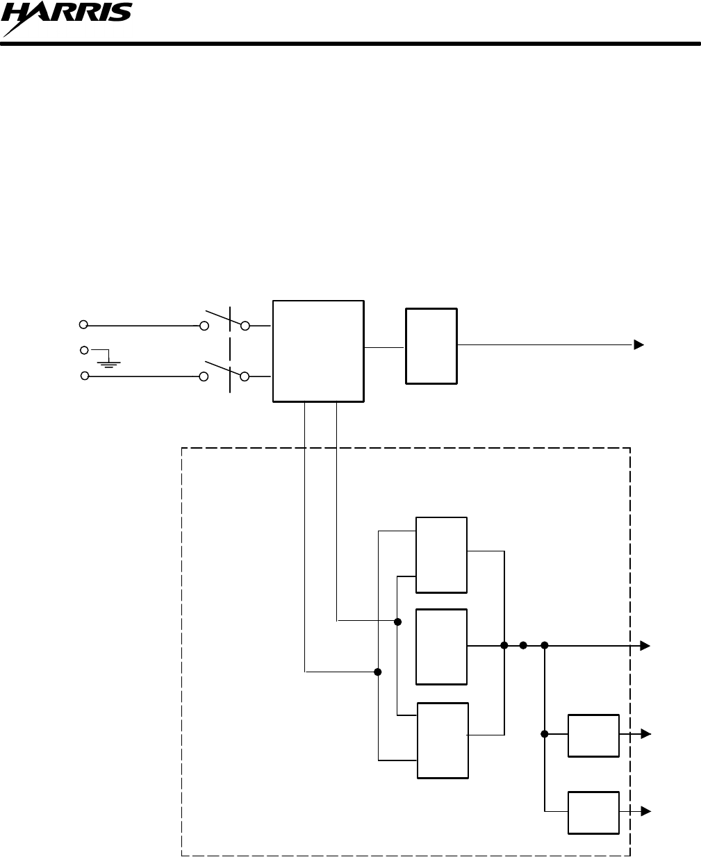
MX-9325
FUNCTIONAL DESCRIPTION
4-17
85 – 265
VAC
POWER
FACTOR
CORRECTION
DC/DC
CONV +28 V
+5 V
+15 V
DC/DC
CONV
DC/DC
CONV
15V
REG
5V
REG
AC HOT
A1A4A2 28 VDC POWER SUPPLY ASSEMBLY
AC NEUTRAL
CB1
DC/DC
CONV +28 V
To A4A1
A1A6 LOW VOLTAGE POWER SUPPLY AS-
SEMBLY
Figure 4-7. Power Distribution Functional Block Diagram
9325-011

MX-9325
FUNCTIONAL DESCRIPTION
4-18
4.4.9.1 EIA-530 Modem
A high speed, short-range synchronous data modem card. The EIA-530 MODEM is utilized to extend the Rear
panel mounted Host Port EIA-530 serial data interface between the local site VGC or MX-9325 and remote site
MX-9325.
The following paragraphs describe the data signal path of the EIA-530 Modem.
4.4.9.1.1 CDP Encoder/Decoder
The receive signal from the EIA-530 Modem TXD input is sent to the CDP encoder and modulates the data.
Similarly, the CDP decoder receives data from the RX input and demodulates the data stream. The
encoder/decoder can be configured for 4-wire full duplex or 4-wire half-duplex. Refer to Chapter 8 for
configuration information.
4.4.9.1.2 Timing Clock
A timing and clock circuit provides the transmit clock to the CDP encoder.
4.4.9.1.3 Transmit Level
The transmit output signal level is configured from 0 to -6 dBm.
4.4.9.1.4 Receive Circuit
A receive filter attenuates unwanted out-of-band frequency content. The automatic equalizer selects the proper
equalization level dependent upon the selected data rate. The AGC provides gain to compensate for transmission
line attenuation.
4.4.9.1.5 Asynchronous / Synchronous Converter
The data is transmitted between modems synchronously. If an asynchronous data signal is input to the modem,
this circuit provides the conversion to synchronous data in compliance with ITU V.22.
4.4.9.1.6 V.54 Loopback Diagnostics
The V.54 loops are activated whether manually from modem front panel pushbutton or via pins 18 and 21 on the
DTE data interface. Pins 18 and 21 adhere to the EIA standard, providing a Type II circuit (EIA-423) bi-polar
signal interface to the DTE. The circuits will provide local analog loopback, local digital loopback and remote
digital loopback. Either the front panel pushbutton or the DTE interface controls may be disabled via jumper
settings. Refer to Chapter 8 for configuration information.
4.4.9.1.7 Test Pattern
The test pattern generator (PATT GENER) facilitates local and remote modem testing with the standard 511
pseudo-random bit pattern. When one of the loopback tests is invoked and the PATT pushbutton on the front panel
is activated, the circuit sends and checks the pattern with an internal Bit Error Rate Tester (BERT). If the BERT
finds errors, the front panel ERROR LED will flicker or remain lit continuously.
4.4.9.1.8 Remote Power Failure (RPF)
This circuit detects an alarm tone transmitted from the remote modem if the remote site power fails. This feature
can only be utilized when an EIA-530 Modem is connected to a remote stand-alone version of the modem. It
cannot be utilized in the modem while in the extender units.
4.4.9.1.9 EIA-530 Modem power Distribution
The EIA-530 Modem interfaces the VHF Extender Unit chassis via a 44-pin card edge connector. The card
receives DC power from the chassis rear panel via the edge connector. The corresponding 5-pin terminal block
and 25-pin connector provide the external interfaces to all signals.

MX-9325
FUNCTIONAL DESCRIPTION
4-19
4.4.9.2 Discrete I/O Card
The Discrete I/O Card is a plug-in card that resides in alternate, even numbered slots of the extender unit. This
card is only required for the extension of Channel Busy and mute signals in split site configurations operating
ACARS or Mode 2. It permits a discrete control signal to be sent or received over a dedicated intersite line. There
are two (2) sections to the circuit, one transmit and one receive. The transmit circuit converts an RS-422 level
input signal to a 20 mA loop interface signal for transmission over twisted pair line in a differential configuration.
The receive circuit performs the opposite conversion function, the loop interface circuit is converted to RS-422
level output signals. The loop receive signal from transmission line interface is also differential. The assembly
contains an alarm function that activates under a variety of fault conditions, such as: Line Open, Line Short,
Absence of RX Signal.
The following paragraphs describe the data signal path of the Discrete I/O Card.
4.4.9.2.1 20mA Loop Transmitter Circuit
A front panel TX indicator (yellow LED) provides polarity status of the transmitting data signal. When the
RS-422 (+) input lead is positive with respect to the (–) lead, the LED will light, indicating a 0 or SPACE (ON)
condition. The 20 mA loop (+) lead will also be positive with respect to the (–) lead. The discrete control signal
(CH BUSY or RX MUTE) state change is applied to the Discrete I/O Card per RS-422 signal standard. The
RS-422 signal passes through a RF filter circuit, then is converted to a TTL signal that is formed into a
differential 20 mA loop signal. The 20 mA loop signal excursions will not exceed 24 volts. This permits
operation over long dedicated transmission lines where loop resistance is measured in 100’s of ohms. A current
limiting circuit is provided to protect the 20 mA loop transmitter from inadvertent transmission line shorts (either
conductor to conductor or conductor to shield). Secondary transient protection is included in the 20 mA loop to
reduce external EMI threats.
4.4.9.2.2 20 mA Loop Transmitter Circuit
The Discrete I/O Card provides an RX indicator (green LED) located on the front panel that provides polarity
status of the received data signal. When the 20 mA loop (+) lead is positive with respect to the (–) lead, the LED
will light, indicating a 0 or space (on) condition present. The RS-422 (+) lead will be positive with respect to the
(–) lead. A DIP switch located on the circuit board may be used to reverse the data sense of the receive circuit.
In the event a transmission fault exists (e.g. a shorted or open transmission line) the front panel ALARM LED
(red) will light and the alarm relay shall provide an output for remote fault indication. The alarm condition may
be reset from the front panel of the Discrete I/O Card or from a remote location via a ground closure input.
Secondary transient protection is applied to the incoming differential 20 mA loop signal to reduce external EMI
threats. The incoming 20 mA signal is translated into separate TTL signals for each current direction, the digital
signals are logically conditioned so that leading and trailing edges of the signals are clean. The signals
representing the differential state are converted into a single TTL signal that may be inverted by way of a DIP
switch if desired. The TTL signal is then converted into an RS-422 standard signal. The RS-422 signal passes
through RF filtering and to the external world.
The alarm circuitry operates on the TTL output before it is converted to RS-422. The alarm detector is simply an
exclusive–OR of the separate TTL signals representing the original differential 20 mA signal. An alarm exists if
the TTL levels are the same. This condition will exist if the transmission line is inadvertently open, closed, or it
the 20 mA loop transmitter fails. A transient fault must exist for at least 10 ms in order to be passed to the alarm
logic. The alarm logic may be reset locally from the front panel of the Discrete I/O Card or from a remote
location. A solid-state relay provides a remote alarm interface. This alarm relay may be configured for either a
normally open or normally closed fault indication.

MX-9325
FUNCTIONAL DESCRIPTION
4-20
4.4.9.2.3 RS-232 Modem (optional)
The RS-232 modem provides an RS-232D (EIA-232/V.24) digital data interface to the VGC. The RS-232 modem
is selected for use in the extender units to support the extension of the optional Antenna Switch Serial Control
Port from the local computer to remote site antenna switches in remote site and split site configurations.
The RS-232 Short Range Modem operates synchronously/asynchronously at speeds up to 19.2 kbps full or
half-duplex over unconditioned lines.
The modem utilizes conditioned differential di-phase modulation (EUROCOM Standard D1) which provides
immunity to background noise and eliminates normal line distortion. This modulation scheme enables efficient
transmission and reception of serial data over unconditioned twisted pair cable.
The following paragraphs describe the data signal path of the RS-232 Modem.
4.4.9.2.4 CDP Encoder/Decoder
The CDP encoder receives data from the TXD (DTE TX Data) input and modulates the data using the conditional
di–phase modulation (CDP) technique. Similarly, the CDP decoder receives data from the (RCV) transmission
line interface and demodulates the receive data stream. The encoder/decoder may be configured for 4-wire full
duplex or 4-wire half-duplex operation. Refer to Chapter 8 for the proper configuration setting.
4.4.9.2.5 Timing Clock
The modulation timing circuit provides the transmit clock to the CDP encoder. There are four clock sources
selectable, dependent upon the mode of operation. The Internal Oscillator (TCX), External Clock (EXT CLK),
or RV CLK clock derived from the receive signal apply to synchronous operation, and should not be selected.
Instead, the ASYNC setting should be used. Refer to Chapter 8 for the proper configuration setting.
4.4.9.2.6 Asynchronous / Synchronous Converter
The data is transmitted over the lines between modems synchronously. When the asynchronous data signal is
input to the modem, this circuit provides the necessary conversion to synchronous data in compliance with ITU
V.22. Frequency deviations between the modem and the DTE up to +/– 1.1% are compensated for by
lengthening/shortening the stop bit every 8 Async characters (12.5%). For frequency deviations from +/–
1.2–2.3%, the stop bits should be lengthened/shortened every four characters (25%). Refer to Chapter 8 for the
proper configuration setting.
4.4.9.2.7 Transmit Level
The transmit output signal (XMT) level may be configured for 0, –3, –6, or –9 dBm. Refer to Chapter 8 for the
proper configuration settings.
4.4.9.2.8 Receive Circuit
The Receive Filter attenuates unwanted out-of-band frequency content. The Automatic Equalizer circuit selects
the proper equalization level dependent upon the selected data rate. The AGC circuit provides gain to compensate
for transmission line attenuation. The AGC operates in one of two modes: continuously ON or controlled by the
DCD line. When the DCD line is active, the AGC is active – when the DCD line is inactive, the AGC will remain
at its last setting level. Refer to Chapter 8 for the proper configuration setting.
NOTE
For full-duplex point-to-point applications, there is no difference
between the Controlled and Continuous AGC modes of
operation.

MX-9325
FUNCTIONAL DESCRIPTION
4-21
4.4.9.2.9 V.54 Loopback Diagnostics
The V.54 loops are activated either manually from the RS-232 Modem front panel or via pins 18 and 21 of the
RS-232 data interface. The circuits will provide Local Analog loopback, Local Digital Loopback and Remote
Digital loopback. Either the front panel pushbuttons or the data interface controls may be disabled via jumper
settings. Refer to Chapter 8 for proper configuration settings.
NOTE
The V.54 delay jumper must be set to OFF to work for
asynchronous operation.
4.4.9.2.10 Remote Power Failure (RPF)
The circuit detects an alarm tone transmitted from the remote modem if the remote site power fails. This feature
can only be utilized when the RS-232 modem is connected to a remote stand–alone version of the modem.
4.4.9.2.11 RS-232 Modem power Distribution
The RS-232 Modem interfaces the extender unit chassis via a 44-pin card edge connector. The card receives DC
power from the chassis rear panel via the edge connector. The corresponding 5-pin terminal block and 25-pin
connector provide the external interfaces to all signals.

MX-9325
FUNCTIONAL DESCRIPTION
4-22
This page intentionally left blank.
MX-9325
TROUBLESHOOTING
5-1
CHAPTER 5
FAULT ISOLATION
5.1 INTRODUCTION
This chapter provides procedures for fault isolation to the assembly level.
5.1.1 Scope of this Chapter
See Figure 5-1. The procedures presented in this chapter assume that the MX-9325 Transceiver is suspected to
have a fault. The maintenance power-on procedure is used to find a fault indication with the unit. If there is a fault
without a BIT code displayed, use the non-BIT fault isolation procedures. If there is a BIT fault code, generated
by running BIT or during normal operation, use the BIT fault isolation procedure. If a TAP is referenced, perform
those procedures. If the problem is not corrected using any of these procedures, use the support data in Chapter 7
based on the functional area of the fault.
Figure 5-1. Fault Isolation Process Used in this Chapter
PROBLEM
REPORTED
MAINTENANCE
POWER-ON
(PARAGRAPH 5.2.1)
BIT FAULT
(PARAGRAPH 5.2.2)
NON-BIT FAULT
(PARAGRAPH 5.2.3)
TROUBLESHOOT USING
THEORY AND SUPPORT
DATA (CHAPTER 7)
RUN-TIME FAULT
(PARAGRAPH 5.2.2)
TROUBLESHOOT USING
TABLES OR TAPs
REMOVE AND REPLACE
SUSPECTED ASSEMBLY
AND REPEAT THIS PROCESS
MX-9325
TROUBLESHOOTING
5-2
5.2 FAULT ISOLATION PROCEDURES
Fault isolation begins with performing the maintenance power-on procedure. The maintenance power-on
procedure references the non-BIT and BIT fault isolation procedures. Refer to Paragraph 5.2.1.
5.2.1 MX-9325 Transceiver Maintenance Power-On Procedure
Table 5-1 is the procedure to power on the MX-9325 Transceiver UUT and execute BIT.
Table 5-1. Maintenance Power-On Procedure
Step Observe Reference
a. Connect a 50-Ohm RF attenuator to
rear panel connector J104.
b. Place PC or terminal POWER switch
in ON position. The PC boots or terminal powers
on. Refer to PC or terminal operation
instructions.
c. If using a PC, run the desired terminal
emulation program. The PC runs the terminal emulation
program. Refer to software operation
instructions for more information.
d. Ensure that the terminal emulation
software or terminal is correctly
configured.
Refer to Chapter 3, Paragraph 3.2.1.
Also refer to terminal or emulation
software operation instructions.
e. Place POWER switch on MX-9325
Transceiver front panel in the ON
position.
The PC or terminal displays the
power-up screen. See Figure
TBD.
If the PC or terminal does not
display the power-up screen, refer
to the non-BIT troubleshooting
procedures in Paragraph 5.2.3.
f. PC or terminal keyboard, type BIT
command: bit v <enter>.If a BIT fault is displayed on the PC
or terminal as a result of the BIT
command, write down the fault
code.
Refer to the BIT troubleshooting
procedures in Paragraph 5.2.2.
g. PC or terminal keyboard, type test
command: tst <enter>.If no errors occur during BIT, con-
tinue operating the radio system in
an attempt to generate a run-time
fault.
If a run-time fault is generated,
refer to the non-BIT troubleshoot-
ing procedures in Paragraph 5.2.3.
If a BIT fault is generated, refer to
the BIT troubleshooting procedures
in Paragraph 5.2.2.
If no fault is generated, return radio
system to operational readiness.
5.2.2 MX-9325 Transceiver BIT Fault Isolation
The MX-9325 Transceiver BIT is a thorough self-test that is run when the MX-9325 Transceiver is powered on.
Additionally, the MX-9325 Transceiver runs continuous BIT while the MX-9325 Transceiver is in use.
To display BIT fault codes, execute BIT using the bit <enter> command. To Display a text (verbose) description
of the BIT fault codes use the bit v <enter> command. Refer to Table 5-2 for a complete listing of BIT fault
codes.
Table 5-2 lists all the BIT fault codes, fault text, and the suspected cause of the fault. The fault codes listed in
Table 5-2 are in the form of hexadecimal readbacks of a binary value. Each code listed is for an individual fault.
More than one fault may occur which will result in a combination of fault codes. When this happens, the binary
value will be combined to be represented as an equivalent hexadecimal readback.

MX-9325
TROUBLESHOOTING
5-3
Example 1: Fault Code [00000014] indicates the Exciter Failure and Directional Coupler Failure.
Example 2: Fault Code [0000000A] indicates the 28 Volt Power Supply Failure and Power Amplifier Failure.
After replacing or repairing the suspected cause of the fault, execute BIT, to see whether the original fault has
been eliminated. If the actions do not correct the problem, proceed to the troubleshooting index in Paragraph
7.6.2.
Table 5-2. BIT Fault Codes, Descriptions, and Suspected Assemblies
Fault Code Fault Text Suspect SRU (Prioritized)
00000001 Low Voltage Power Supply Failure AC Input Voltage,A1A4, A1A6
00000002 28 Volt Power Supply Failure AC Input Voltage, A1A4,A1A6
00000004 Directional Coupler Failure A1A5, A1A2, Antenna
00000008 Power Amplifier Failure A1A4,A1A3
00000010 Exciter Failure A1A3, A1A4, A1A6, A1A2
00000020 Receiver Failure A1A7, A1A4, A1A6, A1A2
00000040 Digital Processor Failure A1A2, A1A4, A1A6
00000080 Unused Unused
00000100 Power Amplifier Heat Sink Low Temp A1A4, A1A2
00000400 Cooling Fan B N/A
00000200 Power Amplifier Heat Sink High Temp A1A4, A1A6, A1A2
00000800 Cooling Fan A N/A
00001000 Rx Sensitivity Low Antenna, A1A5, A1A7, A1A2
00002000 Power Supply Heat Sink Low Temp A1A4, A1A2
00004000 Power Supply Heat Sink High Temp A1A4, A1A2
00008000 System Boot Error A1A2
5.2.3 Non-BIT Fault Isolation
Table 5-3 is a list of the non-BIT fault symptoms. Next to the symptom observed is a reference to the
recommended action to take. When the recommended action is to remove and replace assemblies, replace the
assemblies one at a time in the order listed, testing the UUT (repeat Paragraph 5.2.1) after replacing each
assembly. Chapter 6, Table 6-1, references the assembly removal and replacement procedures. When the
recommended action is to perform a TAP, proceed to the specified TAP. Refer to Paragraph 5.2.5 for more TAP
information. If the actions do not correct the problem, proceed to the fault isolation support data in Chapter 7.
Table 5-3. Non-BIT Fault Symptoms
Symptom Observed Probable
Area Suggested SRU
MX-9325 Transceiver does not power up. Power Supply Proceed to TAP-1. Paragraph 5.2.5.
No RF output Transmit Signal Path A1A2, A1A3, A1A4, A1A5
Weak RF output Transmit Signal Path A1A2, A1A3, A1A4, A1A5
No Receiver Signal Receive Signal Path A1A5, A1A8, A1A7, A1A2
Weak Receiver Signal Receive Signal Path A1A5, A1A8, A1A7, A1A2
Loss of PC/terminal control Data Signal Path A1A2, PC/Terminal

MX-9325
TROUBLESHOOTING
5-4
5.2.4 VHF Extender Unit Diagnostics
The VHF Extender Unit has diagnostics capabilities to perform local analog loopback or local and remote digital
loopback. The loopbacks can be manually activated from a front panel pushbutton switch or remotely via a
control signal to the rear panel interface connector from the VGC.
The VHF Extender Unit must be properly installed into a system and AC power applied to perform diagnostics.
Refer to Chapter 8, Paragraph 8.4.6.
Table 5-4 lists the VHF Extender Unit diagnostic tests and suspected SRU. Refer to Chapter 6, Corrective
Maintenance for removal and replacement procedures. Refer to Chapter 2, Paragraph 2.2 for front panel control
and indicator descriptions.
Table 5-4. VHF Extender Unit Diagnostic Test
Diagnostic Pushbutton Switch Observe Suggested SRU
EIA-530 Modem DIG TEST LED Blinks Red EIA-530 Modem, Intersite lines
EIA-530 Modem ANA TEST LED Blinks Red EIA-530 Modem, Intersite lines
EIA–530 Modem REM TEST LED Blinks Red EIA-530 Modem, Intersite lines
EIA-530 Modem PATT TEST LED Blinks Red
ERR LED Blinks Yellow EIA-530 Modem, Intersite lines
Discrete I/O Card (no pushbutton present) ALM Lights Red Discrete I/O Card, Intersite lines
RS-232 Modem DIG TEST LED Blinks Red RS-232 Modem, Intersite lines
RS-232 Modem ANA TEST LED Blinks Red RS-232 Modem, Intersite lines
RS-232 Modem REM TEST LED Blinks Red RS-232 Modem, Intersite lines
5.2.5 TAPs
TAPs are provided to help the technician isolate faults using procedures other than simple assembly swapping.
Each TAP begins with a simple description of the fault or symptom.
When applicable, begin by performing the listed initial checks. These are checks that can be performed without
the use of tools or test equipment. If the initial checks do not solve the problem, continue by performing the
procedure itself. Assembly and module removal and replacement procedures are located in Chapter 6, Corrective
Maintenance. If the problem still exists after completing the TAP, proceed to the fault isolation support data in
Chapter 7.

MX-9325
TROUBLESHOOTING
5-5
TAP-1: NO POWER
The MX-9325 Transceiver does not power on.
INITIAL CHECKS
Ensure that AC power is supplied to the
MX-9325 Transceiver.
Ensure that the MX-9325 Transceiver front panel AC
power switch is in the on position.
PROCEDURE
Check for the following voltages at the location provided:
A1A6J4 Pin 1 +28 Vdc
A1A6J4 Pin 2 +15 Vdc
A1A6J4 Pin 3 + 5 Vdc
A1A6J4 Pin 5 +–15 Vdc
Are all voltages present?
YN
Are some of these voltages present?
YN
Disconnect power connector A1A4A2J3 to
A1A4A2 Power Supply Assembly. Check
cable for the following voltages:
87 to 230 Vac – Pins 3 and 4
Is voltage present?
YN
Disconnect power connector
A1A4A2J3 to A1A4A2 Power
Supply Assembly. Check cable
for the following voltages:
87 to 230 Vac – Pins
1 and 2
Is voltage present?
YN
Remove and replace
AC input cable.
Return unit to
operation.
Remove and replace CB1 on
Front Panel Assembly. Return
unit to operation.
Remove and replace A1A4 Assembly.
Return unit to operation.
Remove and replace A1A6 Assembly. Return unit to
operation.
Remove and replace A1A2 Assembly. Return unit to operation.

MX-9325
TROUBLESHOOTING
5-6
This page intentionally left blank.
MX-9325
MAINTENANCE
6-1
CHAPTER 6
MAINTENANCE
6.1 INTRODUCTION
This chapter provides the maintenance procedures for the MX-9325 Transceiver. Paragraph 6.2 provides
preventive maintenance procedures. Paragraph 6.3 provides scheduled maintenance procedures. Paragraph 6.5
provides corrective maintenance which includes adjustment and alignment procedures and assembly removal and
replacement procedures. The MX-9325 Transceiver assemblies are listed in Table 6-1 with a reference to the
corresponding removal and replacement procedure paragraph. For parts list and family tree information, refer to
Chapter 7, Paragraph 7.4.
Table 6-1. MX-9325 Transceiver Assembly Removal and Replacement Paragraph References
SRU Name Paragraph
Reference
MX-9325 Transceiver 6.5.1
A1A2 Digital PWB Assembly 6.5.2
A1A3 Exciter PWB Assembly 6.5.3
A1A4 Heatsink Assembly 6.5.4
A1A5 Low Pass Filter & Directional Coupler Assembly 6.5.5
A1A6 Low Voltage Power Supply Assembly 6.5.6
A1A7 Receiver PWB Assembly 6.5.7
A1A8 Helical Filter Assembly 6.5.8
Table 6-2. VHF Extender Unit Assembly Removal and Replacement Paragraph References
SRU Name Paragraph
Reference
VHF Extender Unit 6.5.9
VHF Extender Unit Circuit Card 6.5.10
NOTE
If a product has been fielded for several years, there is the
possibility of firmware incompatibility between new replacement
assemblies and an older unit. If unsure of compatibility, contact
Harris RF Communications customer service department (tel:
716-244-5830).
MX-9325
MAINTENANCE
6-2
6.2 PREVENTIVE MAINTENANCE
No periodic (preventive) maintenance or electronic adjustments are required for the MX-9325 Transceiver or
VHF Extender Unit. All that is recommended is periodic cleaning and inspection.
6.2.1 List of Preventive Maintenance Procedures
Table 6-3 lists the preventive maintenance procedures recommended for the MX-9325 Transceiver and VHF
Extender Unit. The table is divided into the following columns:
a. Column 1 – Paragraph Number, where the procedure begins.
b. Column 2 – Preventive Maintenance Procedure, describes the test to be performed.
c. Column 3 – Periodicity, interval in which the procedure should be performed (that is; daily, weekly,
monthly, etc.).
Table 6-3. Preventive Maintenance Procedures
Paragraph
Number Preventive Maintenance
Procedure Periodicity
6.2.2 Clean and inspect chassis
exterior. Semi-annual
6.2.3 Clean and inspect chassis
interior. During repair
6.2.2 Clean and Inspect Chassis Exterior
Refer to Chapter 7, Paragraph 7.3 for a list of tools and materials. Perform the following procedure to clean and
inspect the MX-9325 Transceiver exterior:
WARNING
Failure to remove electrical connections from the unit can cause
injury or death to personnel.
NOTE
When the MX-9325 Transceiver is supplied as part of a system,
the system documentation takes precedence.
a. At MX-9325 Transceiver front panel, verify power switch is in the OFF position.
b. Disconnect AC power at the source.
c. Inspect MX-9325 Transceiver exterior for:
1. Physical damage
2. Loose hardware including knobs and switches
3. Accumulated dust and/or other foreign matter

MX-9325
MAINTENANCE
6-3
d. Use a clean lint-free cloth (Item 10) to wipe exterior surfaces.
e. Connect AC power at the source.
6.2.3 Clean and Inspect Chassis Interior
Refer to Chapter 7, Paragraph 7.3 for a list of tools and materials. Perform the following procedure to clean and
inspect the MX-9325 Transceiver interior before and during repair:
WARNING
Failure to remove electrical connections from the unit could
cause injury or death.
a. Use a flat-tip screwdriver (Item 1) to remove the (9) screws that secure MX-9325 Transceiver top cover
to chassis. Remove the top cover.
b. Use service-vacuum cleaner (Item 11) to remove any accumulated dust from the chassis interior.
c. Inspect MX-9325 Transceiver interior for:
1. Foreign matter
2. Discolored or scorched components
3. Loose or damaged circuit cards or connectors
4. Moisture
5. Stripped threaded holes
d. Replace MX-9325 Transceiver top cover. Use a flat-tip screwdriver (Item 1) to replace the nine (9) screws
that secure exciter top cover to chassis.
6.3 SCHEDULED MAINTENANCE
The following provides scheduled maintenance for the MX-9325 Transceiver. Scheduled maintenance should be
performed annually upon completion of a service task. All scheduled maintenance procedures should pass test
before the MX-9325 Transceiver is put back into operation.
6.3.1 Scheduled Maintenance Procedure List
Table 6-4 lists the scheduled maintenance procedures recommended for the MX-9325 Transceiver. The table is
divided into the following columns:
a. Column 1 – Paragraph Number, where the procedure begins.
b. Column 2 – Scheduled Maintenance Procedure, describes the test to be performed.
c. Column 3 – Periodicity, interval in which the procedure must be performed (that is, daily, weekly,
monthly, annually, etc.).

MX-9325
MAINTENANCE
6-4
Table 6-4. Scheduled Maintenance Test Procedures
Paragraph
Number Scheduled Maintenance
Test Procedure Periodicity
6.4.1 BIT Annually
6.4.2 LED Test Annually
6.4.3 Rx Sensitivity and Distortion Annually
6.4.4 Tx Power Output and Distortion Annually
6.4.5 Tx 2:1 VSWR Load Annually
6.4.6 Tx Time–out Annually
6.4.7 Tx Spurious Suppression Annually
6.3.2 Recommended Test Equipment
Refer to Chapter 7, Table 7-2 for a list of recommended test equipment to perform scheduled maintenance
test procedures.
NOTE
Most test functions can be performed by a communications test
set, or service monitor, which performs the combined functions
of RF and audio signal generator, frequency counter, modulation
analyzer, and RF wattmeter. Service monitors are typically
equipped with an input attenuator pad/dummy load that allows
the full output of the MX-9325 Transceiver to be coupled
directly to the instrument. If this feature is not provided, a
separate pad/dummy load will be required. Separate instruments
can also be used, but this is usually not practical for field work.
Suitable service monitors are manufactured by Hewlett Packard,
the IFR Division of Regency, Inc., and Marconi Instruments Ltd.
NOTE
The frequency measuring instrument (counter, etc.) must have a
high stability time base (better than 0.1 ppm) to ensure accuracy.
Do not attempt to set the reference frequency unless the test
equipment conforms.
6.4 SCHEDULED MAINTENANCE PROCEDURES
The following paragraphs contain information about tests to be performed on a MX-9325 Transceiver as part of
scheduled maintenance.
6.4.1 MX-9325 Transceiver BIT Test
The following paragraphs provide instructions for performing the MX-9325 Transceiver BIT test as part of
scheduled maintenance.
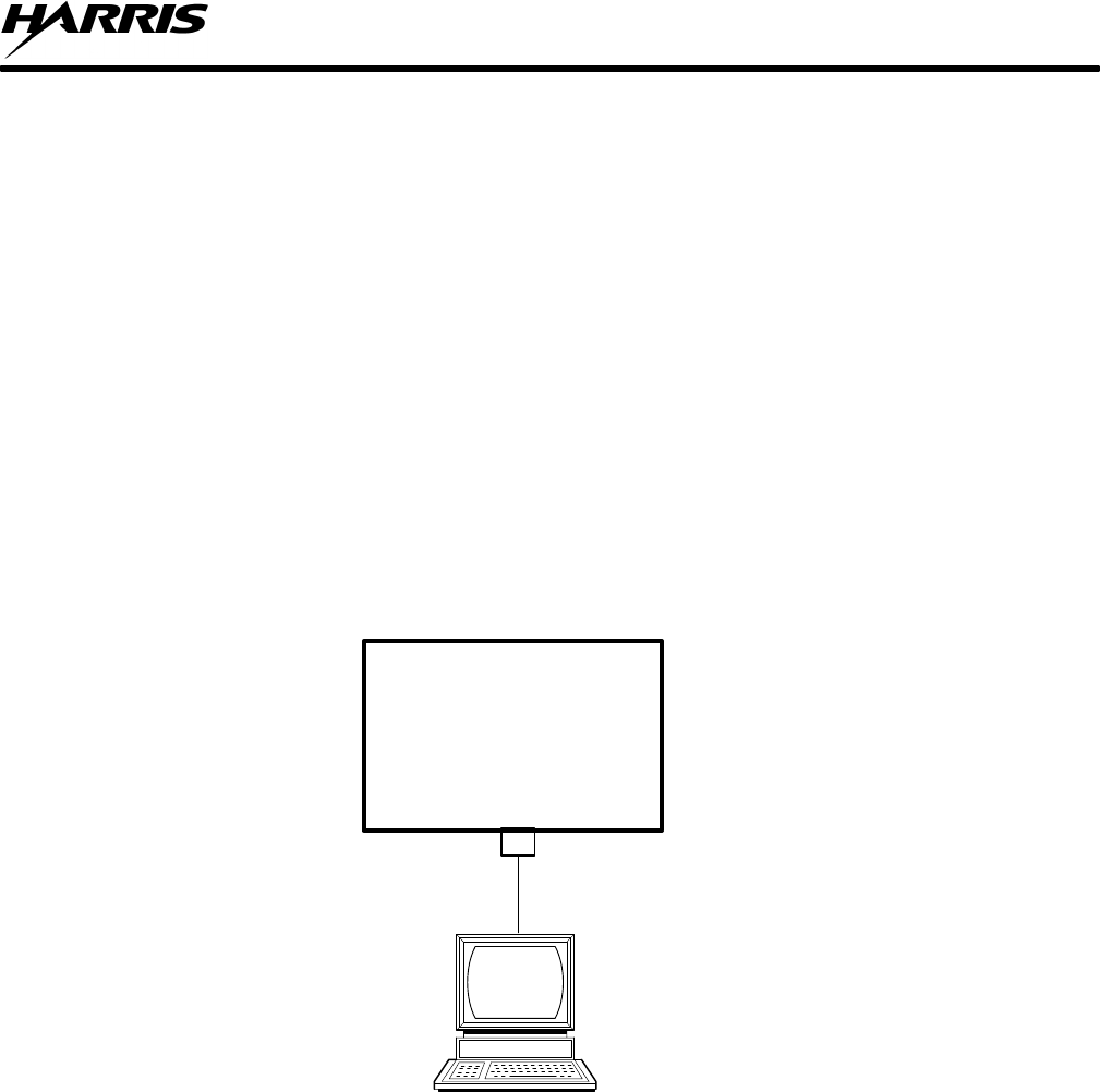
MX-9325
MAINTENANCE
6-5
6.4.1.1 Required Equipment
The following equipment is required to perform the power output test:
•PC or ASCII Terminal
6.4.1.2 Test Procedure
Perform the following procedure to perform the MX-9325 Transceiver BIT test:
a. Set up the radio system as shown in Figure 6-1.
b. Use PC/terminal to set MX-9325 Transceiver UUT frequency to 127.000 MHz.
c. On PC/terminal enter his command to display the history of all BIT faults codes which have occurred
since the last time the historical BIT status word was cleared.
d. On PC/terminal enter dbt command to obtain detailed BIT results for each assembly in the radio.
e. If any of the detailed BIT results are non–zero, refer to Chapter 5, Paragraph 5.2.2 for BIT fault isolation.
Figure 6-1. MX-9325 Transceiver BIT Test Set Up
PC/TERMINAL
MX-9325 TRANSCEIVER
UNIT UNDER TEST
FRONT PANEL
MAINTENANCE
CONNECTOR
9325-012

MX-9325
MAINTENANCE
6-6
6.4.2 MX-9325 Transceiver LED Test
The following paragraphs provide instructions for performing the MX-9325 Transceiver LED test as part of
scheduled maintenance.
6.4.2.1 Required Equipment
The following equipment is required to perform the MX-9325 Transceiver LED test:
•Signal Generator
•PC or ASCII Terminal
6.4.2.2 Test Procedure
Perform the following procedure to test the MX-9325 Transceiver front panel LEDs:
a. Set up the radio system as shown in Figure 6-2. Refer to Chapter 3, Paragraph 3.2.4 for command
information.
b. Verify that the AC POWER LED lit when the power switch was turned on.
c. Apply a –60 dBm receive signal to the J5 antenna port.
d. Verify that the RECEIVE LED lit.
e. On PC/terminal, enter key on command to key the MX-9325 Transceiver.
f. Verify that the TRANSMIT LED lit.
g. On PC/terminal, enter key off command to unkey the MX-9325 Transceiver.
h. Remove the MX-9325 Transceiver bottom cover.
i. Simulate a critical fault by removing the coaxial cable from J21 on the A1A2 Digital PWB Assembly.
j. Verify that the FAULT LED lit.
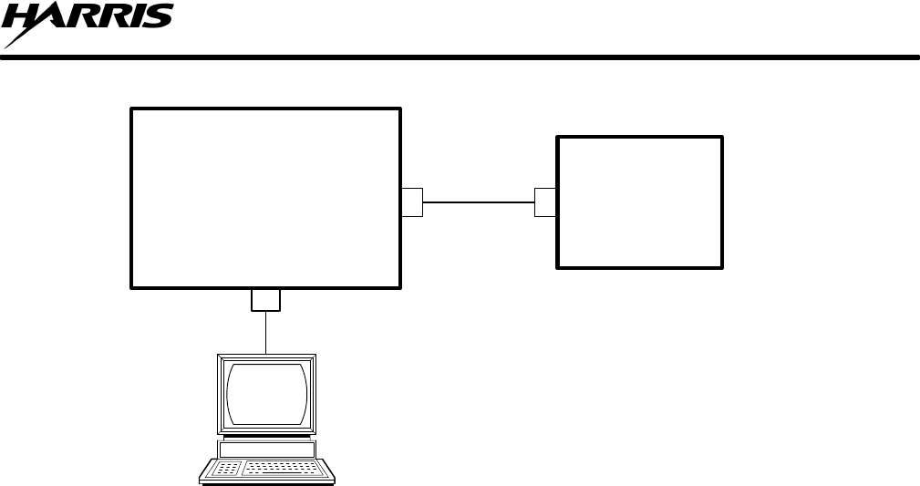
MX-9325
MAINTENANCE
6-7
Figure 6-2. MX-9325 Transceiver LED Test Set Up
SIGNAL
GENERATOR
PC/TERMINAL
J5
ANTENNA
MX-9325 TRANSCEIVER
UNIT UNDER TEST
9325-013
FRONT PANEL
MAINTENANCE
CONNECTOR
6.4.3 Receive Sensitivity and Distortion Test
Performs a series of receive sensitivity tests by reading the SINAD at a single specified drive level.
The following paragraphs provide instructions for performing the Receive Sensitivity and Distortion test as part
of scheduled maintenance.
6.4.3.1 Required Equipment
The following equipment is required to perform the Receiver Sensitivity and Distortion test:
•RF signal generator
•30 dB attenuator
6.4.3.2 Test Procedure
Perform the following procedure to test the MX-9325 Transceiver: Receive Sensitivity and Distortion
a. Set up the radio system as shown in Figure 6-3. Refer to Chapter 3, Paragraph 3.2.4 for command
information.
b. Configure the audio analyzer to measure SINAD.
c. Use PC/terminal frq command to set MX-9325 Transceiver to receive AM at a test frequency of 127.500
MHz .
d. Set the signal generator to the test frequency with AM modulation of a 1 kHz tone at 30% modulation.
e. Adjust the signal generator to provide –99.0 dBm at the antenna port of the MX-9325 Transceiver
(accounting for path loss through the attenuator, cables, and switches).
f. Measure the SINAD on the audio analyzer. The measurement should be > or = 10 dB.
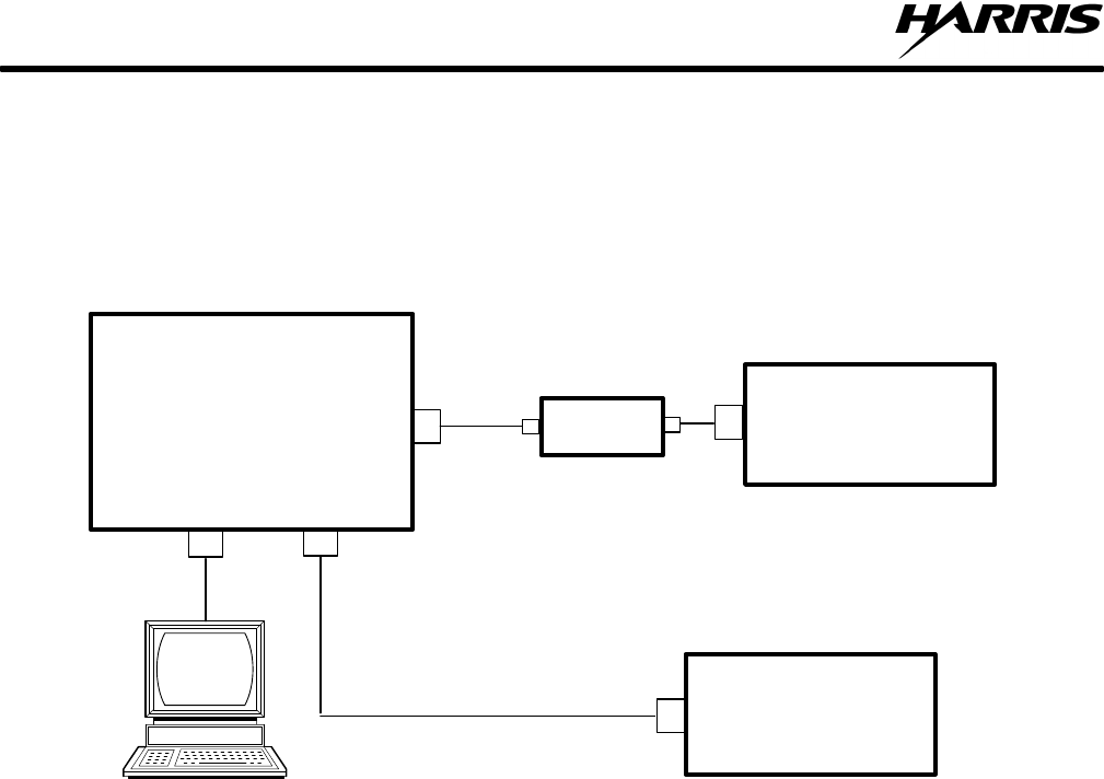
MX-9325
MAINTENANCE
6-8
g. Adjust the signal generator to –60.0 dBm (at the antenna port of the MX-9325 Transceiver) and measure
the distortion on the audio analyzer.
h. Measure the distortion on the audio analyzer. The measurement should be <5 dB.
i. Repeat Steps c through h using test frequencies of 118 MHz and 136.975 MHz.
Figure 6-3. MX-9325 Transceiver Receive Sensitivity and Distortion Test Set Up
SIGNAL
GENERATOR
PC/TERMINAL
9325-014
MX-9325 TRANSCEIVER
UNIT UNDER TEST
FRONT PANEL
MAINTENANCE
CONNECTOR
FRONT PANEL
ACCESSORY
PORT
(J9-3)
AUDIO
ANALYZER
AUDIO IN HI
J5
ANTENNA
PORT 30 DB
ATTENUATOR
6.4.4 Transmit Power Output and Distortion
Performs a series of tests of transmit power output level, percent modulation, and distortion at various carrier
frequencies.
The following paragraphs provide instructions for performing the Transmit Power Output test as part of scheduled
maintenance.
6.4.4.1 Required Equipment
The following equipment is required to perform the percent modulation test:
•30 dB, 50-Ohm Attenuator
•RF Power Meter
•Modulation Analyzer
•PC or ASCII Terminal
6.4.4.2 Test Parameters
The following are the power outputs to be tested:
•Power Output at high power mode, 25 Watts ±5%

MX-9325
MAINTENANCE
6-9
•Power Output at medium power mode, 10 Watts ±5%
•Power Output at low power mode, 2 Watts ±5%
6.4.4.3 Test Procedure
The Transmit Power Output and Distortion Tests are done at high power mode using carrier frequencies at
118.0 MHz, 126.9 MHz, 127.1 MHz and 136.975 MHz.
The Transmit Power Output and Distortion Tests are done at medium and low power mode using a carrier
frequency at 136.975 MHz. only.
Perform the following procedure to test the Transmit Output Power and Distortion of the MX-9325 Transceiver:
a. Set up the radio system as shown in Figure 6-4. Refer to Chapter 3, Paragraph 3.2.4 for command
information.
b. Use PC/terminal enter frq command to set the frequency of the MX-9325 Transceiver to 136.975 MHz.
c. Use PC/terminal enter mod acars command to set MX-9325 Transceiver UUT to transmit AM.
d. Use PC/terminal enter pwr command to set MX-9325 Transceiver UUT to transmit the specified power.
e. Use PC/terminal enter mdl 50 command to set MX-9325 Transceiver UUT to transmit the operating
frequency with 50% modulation of the 1 kHz internal test tone.
f. On PC/terminal, enter key on command to key the MX-9325 Transceiver.
g. Measure the power level (in dBm) from the power meter, and correct for the directional coupler and cable
loss to calculate the power output directly at the antenna port.
h. On the modulation analyzer, measure the actual AM percent modulation of the radio’s transmission and
verify measurement is ±5% at 50% AM modulation.
i. On the audio analyzer, measure the distortion of the demodulated audio output of the modulation analyzer
and verify measurement is < 5%.
j. If the modulation appears distorted, check power supply voltages.
k. If distortion is still present, replace A1A4 Heatsink Assembly, then A1A3 Exciter PWB Assembly, and
A1A2 Digital PWB Assembly.
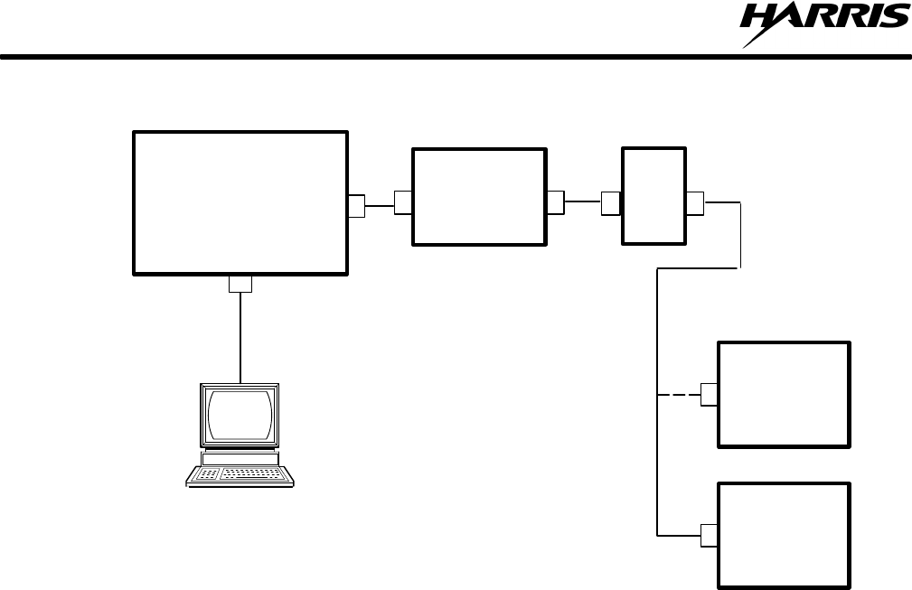
MX-9325
MAINTENANCE
6-10
Figure 6-4. MX-9325 Transceiver Transmit Power Output and Distortion Test Setup 9325-016
PC/TERMINAL
J5 30 dB
ATTENUATOR
AUDIO
ANALYZER
MODULATION
ANALYZER
MX-9325 TRANSCEIVER
UNIT UNDER TEST
FRONT PANEL
MAINTENANCE
CONNECTOR
POWER
METER
6.4.5 MX-9325 Transceiver VSWR Load
Verifies performance of the MX-9325 Transceiver into a load with a 2:1 VSWR and verifies the radio’s internal
directional coupler by reading back the forward and reflected power.
The following paragraphs provide instructions for performing the MX-9325 Transceiver VSWR load test as part
of scheduled maintenance.
6.4.5.1 Required Equipment
The following equipment is required to perform the MX-9325 Transceiver VSWR load test:
•RF Power Meter
•Audio Analyzer
•Modulation Analyzer
•50 Ohm Load
•50 Ohm Attenuator
•BNC T Connector
•PC or ASCII Terminal
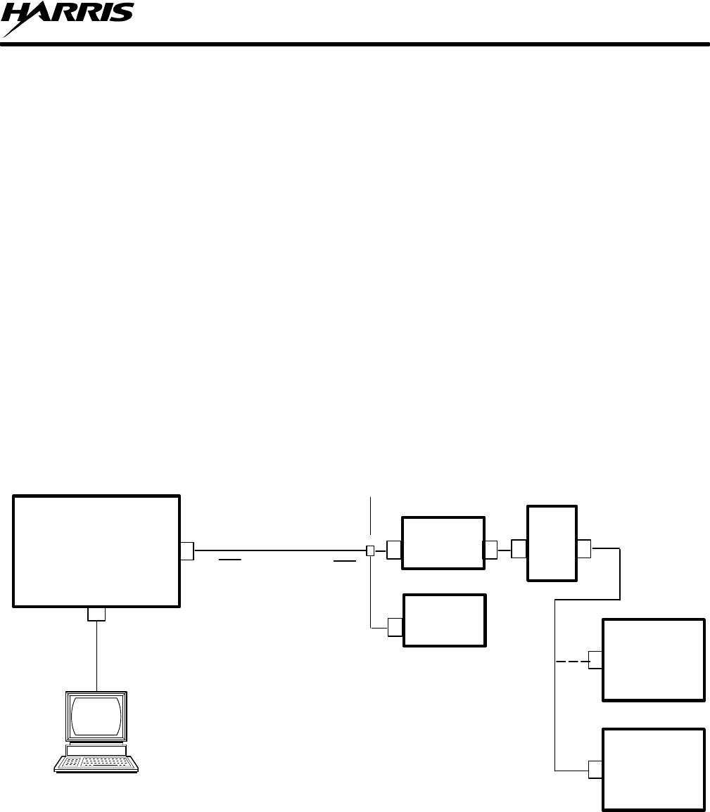
MX-9325
MAINTENANCE
6-11
6.4.5.2 Test Procedure
Perform the following procedure to test the VSWR Load of the Transceiver:
NOTE
The 2:1 load is constructed by connecting a 50 ohm attenuator
and a 50 ohm load together with a BNC T. To present an
effective 25 ohm load at the antenna connector, the total cable
length (including switching) from the antenna port to the T must
be an integer multiple of half the wavelength. For 136.975 MHz,
this length is approximately 1.09 meters.
a. Set up the test bed radio system as shown in Figure 6-5. Refer to Chapter 3, Paragraph 3.2.4 for command
information.
b. Refer to Paragraph 6.4.4. Repeat the Transmit Power Output and Distortion test procedure using a carrier
frequency of 136.975 MHz and power output at 25.0 WATTS.
c. On PC/terminal, read the forward power of the transmission using the fpw <enter> command.
d. On PC/terminal, read the reverse power of the transmission using the rpw <enter> command.
Figure 6-5. MX-9325 VSWR Load Test Set Up
2205-016
PC/TERMINAL
J5 30 dB
ATTENUATOR
AUDIO
ANALYZER
MODULATION
ANALYZER
MX-9325 TRANSCEIVER
UNIT UNDER TEST
FRONT PANEL
MAINTENANCE
CONNECTOR
POWER
METER
50 OHM
LOAD
APPROXIMATE
CABLE LENGTH
1.09 METERS
"
BNC
T
CONNECTOR

MX-9325
MAINTENANCE
6-12
6.4.6 MX-9325 Transceiver Transmit Time-Out test
Verifies the MX-9325 Transceivers continuous key timer. The time-out specified is the number of seconds the
MX-9325 Transceiver may be keyed continuously before it will automatically unkey.
The following paragraphs provide instructions for performing the MX-9325 Transceiver Transmit Time-Out Test
as part of scheduled maintenance.
6.4.6.1 Required Equipment
The following equipment is required to perform the MX-9325 Transceiver Transmit Time-Out Test:
•RF Power Meter
•50 Ohm Load
•PC or ASCII Terminal
6.4.6.2 Test Procedure
Perform the following procedure to execute the MX-9325 Transceiver Transmit Time-Out Test:
a. Set up the test bed radio system as shown in Figure 6-5. Refer to Chapter 3, Paragraph 3.2.4 for command
information.
b. On PC/terminal, enter tim 3 command to set the transmitter continuous key time–out interval to 3
seconds.
c. On PC/terminal, enter pwr 10 command to set the transmit power output level to 10 Watts.
d. On PC/terminal, enter key on command to key the MX-9325 Transceiver.
e. After keying for a total of 2 seconds, measure the power output on the power meter and verify the
measurement is 10 Watts ±5%.
f. After keying for a total of 4 seconds, measure the power output on the power meter and verify the
measurement is 0 Watts ±0.1.
g. On PC/terminal, enter key off command to unkey the MX-9325 Transceiver.
h. Return the time-out interval to the desired value using the tim command.
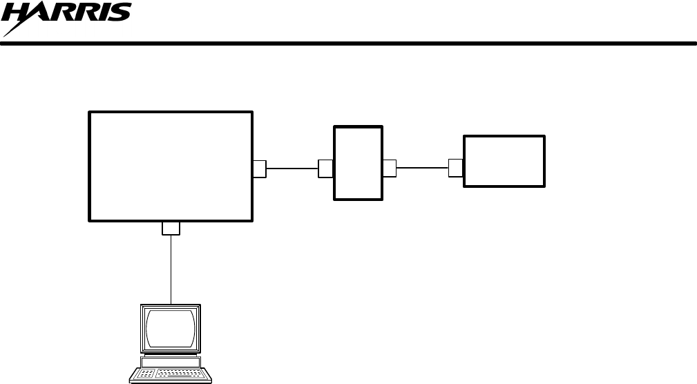
MX-9325
MAINTENANCE
6-13
PC/TERMINAL
J5
MX-9325 TRANSCEIVER
UNIT UNDER TEST
FRONT PANEL
MAINTENANCE
CONNECTOR
POWER
METER
50 OHM
LOAD
Figure 6-6. MX-9325 Transceiver Transmit Time–out
2205-033
6.4.7 MX-9325 Transceiver Transmit Spurious Suppression
Performs a series of spurious suppression tests at various transmit frequencies. For each frequency, the MX-9325
Transceiver UUT will be keyed and the frequency spectrum from 118.0 to 137.0 MHz will be analyzed for spurs
that may indicate improper circuit operation of the PA, exciter, power supply, etc.
The following paragraphs provide instructions for performing the MX-9325 Transceiver Transmit Spurious
Suppression Test as part of scheduled maintenance.
6.4.7.1 Required Equipment
The following equipment is required to perform the MX-9325 Transceiver Transmit Spurious Suppression Test:
•30 dB Attenuator
•Spectrum Analyzer
•PC or ASCII Terminal
6.4.7.2 Test Procedure
The MX-9325 Transceiver Transmit Spurious Suppression Tests are done at a 25 Watt power output using
operating frequencies at 118.0 MHz, 126.9 MHz, 127.1 MHz and 136.975 MHz.
Perform the following procedure to execute the MX-9325 Transceiver Transmit Spurious Suppression Test:
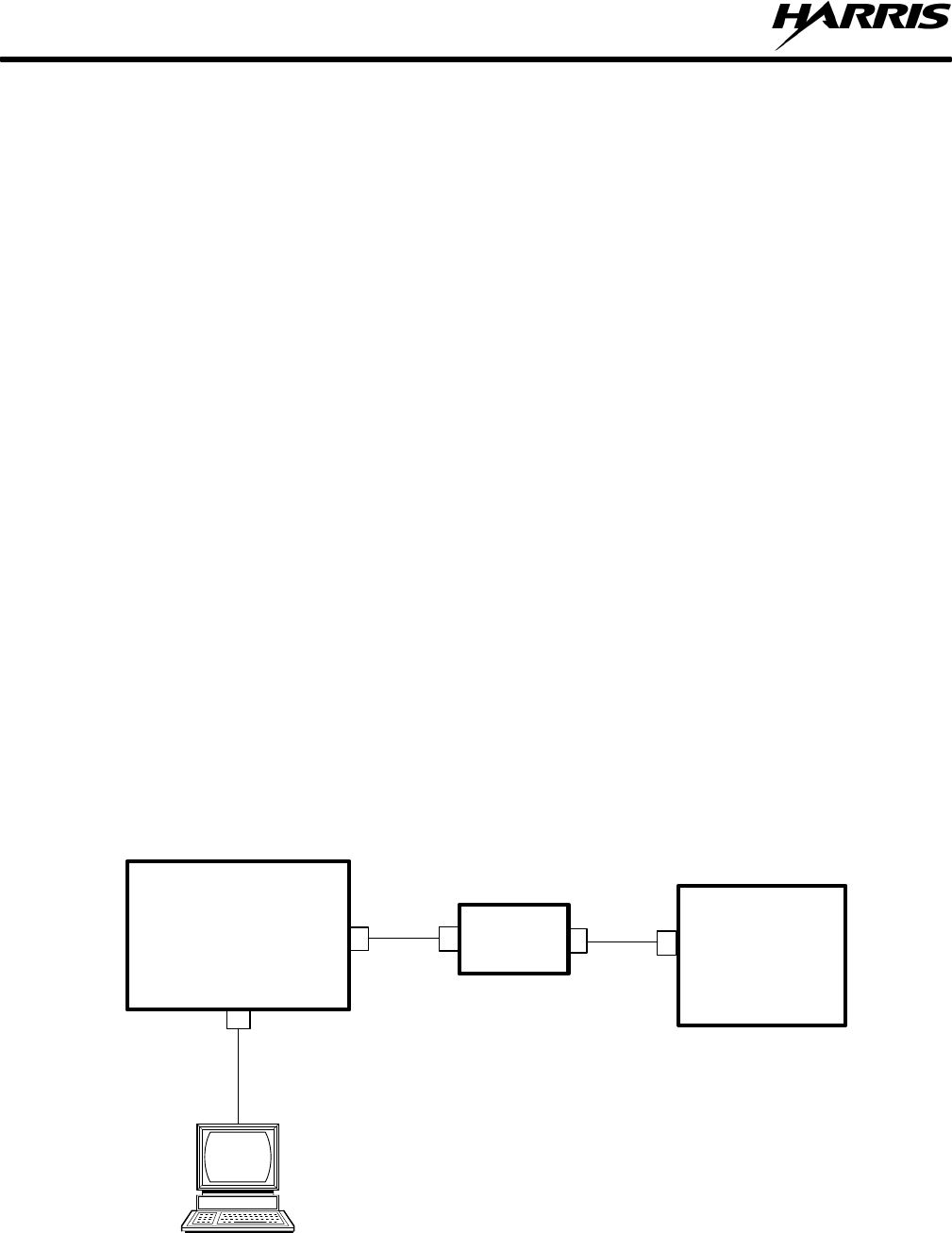
MX-9325
MAINTENANCE
6-14
NOTE
The suppression level, specified as a positive value, represents
the amount of suppression below the carrier amplitude. For
example 60 dB of suppression indicates that the amplitude of the
spur relative to the carrier is –60 dBc.
a. Set up the test bed radio system as shown in Figure 6-7. Refer to Chapter 3, Paragraph 3.2.4 for command
information.
b. Use PC/terminal enter frq command to set the frequency of the MX-9325 Transceiver to desired carrier
frequency.
c. Use PC/terminal enter pwr command to set the output power of the MX-9325 Transceiver to 25 Watts.
d. Set the spectrum analyzer of the RF communications test set to sweep from 118.0 to 137.0 MHz.
e. Use PC/terminal enter key on command to key the MX-9325 Transceiver.
f. Inspect the entire spectrum analyzer waveform for any spurs which have an amplitude greater than the
carrier amplitude minus the suppression of 60-dB. For example a carrier with an amplitude of 100 dB,
count the spurs that occur after 40-dB.
g. Do not count the fundamental in the spur analysis. For example discard spurs that occur within 2 MHz of
the carrier frequency.
h. If any spurs are within 2 MHz of each other, assume that this is a single spur with a wide bandwidth and
record the frequency and level in this region at which the maximum peak occurs.
i. Record the resulting number of spurs detected.
j. Use PC/terminal enter key off command to unkey the MX-9325 Transceiver.
PC/TERMINAL
J5
MX-9325 TRANSCEIVER
UNIT UNDER TEST
FRONT PANEL
MAINTENANCE
CONNECTOR
SPECTRUM
ANALYZER
30 dB
ATTENUATOR
Figure 6-7. MX-9325 Transceiver Transmit Spurious Suppression Test Set up
2205-034
MX-9325
MAINTENANCE
6-15
6.5 CORRECTIVE MAINTENANCE
The following provides corrective maintenance procedures consisting of adjustments and alignments, and removal
and replacement procedures.
6.5.1 MX-9325 Transceiver Removal and Replacement Procedure
Refer to Chapter 7, Paragraph 7.3 for a list of tools. See Figure 6-8 for typical MX-9325 Transceiver rack
mounting. The following paragraphs provide instructions for the removal and replacement of the MX-9325
Transceiver.
WARNING
Failure to remove electrical connections from the unit could
cause injury or death.
CAUTION
Failure to take the proper precautions may damage the assembly
due to static discharge.
6.5.1.1 MX-9325 Transceiver Removal
Perform the following procedure to remove the MX-9325 Transceiver from the equipment rack:
a. Set the equipment rack POWER ON switch to the OFF position. Set the MX-9325 Transceiver AC
POWER switch to the OFF position. Disconnect power to rack and extender unit.
b. Use a No. 2 cross-tip screwdriver (item 1) to remove four (4) screws that secure the MX-9325
Transceiver front panel to the equipment rack.
c. Use the handles to pull the unit forward until the slides are fully extended and in the locked position.
d. Disconnect the power cable from the MX-9325 Transceiver AC power input connector. Disconnect all
other connections to the MX-9325 Transceiver rear panel.
e. Press the slide release button, and remove the MX-9325 Transceiver from the rack by pulling it forward
until it clears the slides.
f. Place the unit on a steady work surface.
g. Push the extended rack slides back into the rack.
6.5.1.2 MX-9325 Transceiver Replacement
Perform the following procedure to replace the MX-9325 Transceiver into the equipment rack:
a. Pull the rack portion to the slides from the equipment rack until they are fully extended and locked.
b. Install the MX-9325 Transceiver to the slides and push into the equipment rack until the slides lock.
c. Connect the power cable to the MX-9325 Transceiver AC power input connector. Connect all other
required electrical connections to the MX-9325 Transceiver rear panel connectors.

MX-9325
MAINTENANCE
6-16
d. Press the release tabs on the slides and push the unit into the equipment rack.
e. Use No. 2 cross-tip screwdriver (item 1) to replace the four (4) screws that secure the MX-9325
Transceiver front panel to the equipment rack.
f. Apply AC power to equipment rack. Set the equipment rack POWER ON switch to the ON position. Set
the MX-9325 Transceiver POWER ON switch to the ON position.
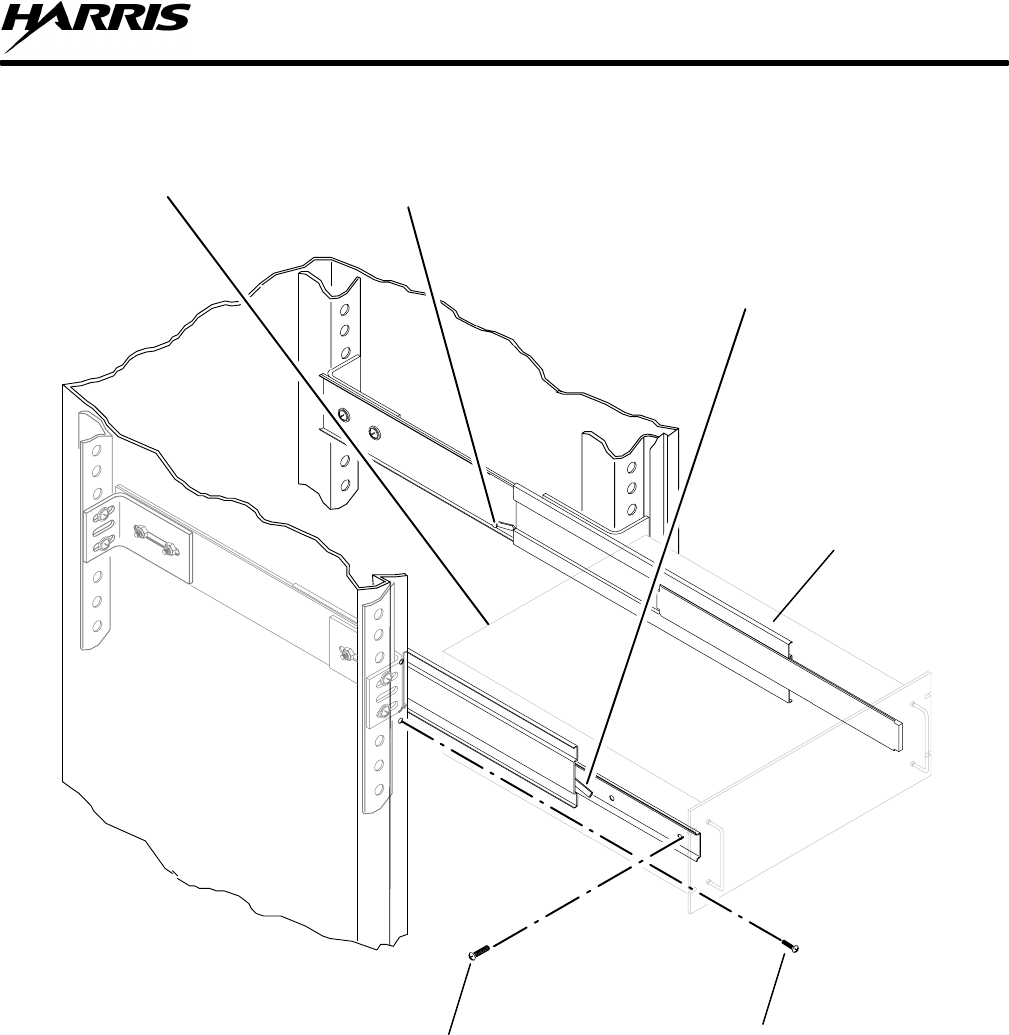
MX-9325
MAINTENANCE
6-17
Figure 6-8. MX-9325 Transceiver Rack Mounting Details
9325-017
LIFT UP TO UNLOCK SLIDE MECHANISM
(BOTH SIDES OF UNIT SIMULTANEOUSLY).
DISCONNECT CABLING
BEFORE REMOVING UNIT.
UNIT SHOWN IN
FULLY EXTENDED
POSITION.
SLIDE LOCKS ON
BOTH SIDES
FRONT PANEL
SCREWS
(4 PLACES)
SCREWS
(8 PLACES)
MX-9325
MAINTENANCE
6-18
6.5.2 A1A2 Digital PWB Assembly
Refer to Chapter 7, Paragraph 7.3 for a list of tools. See Figure 7-2 for hardware and component locations. The
following paragraphs provide instructions for the removal and replacement of A1A2 Digital PWB Assembly.
WARNING
Failure to remove electrical connections from the unit could
cause injury or death.
CAUTION
Failure to take the proper precautions may damage the assembly
due to static discharge.
6.5.2.1 A1A2 Digital PWB Assembly Removal
Perform the following procedure to remove A1A2 Digital PWB Assembly from the MX-9325 Transceiver:
a. Set the equipment rack POWER ON switch to the OFF position. Set the MX-9325 Transceiver AC
POWER switch to the OFF position. Disconnect power to rack and MX-9325 Transceiver.
b. Refer to Paragraph 6.5.1. Remove MX-9325 Transceiver from equipment rack.
c. Use flat tip screwdriver (item 6) to loosen 10 captive screws that secure the top cover MP1 to the chassis.
Remove the cover.
d. Disconnect the following connectors:
•A1A2J11
•A1A2J3
•A1A2J12
•A1A2J28
•A1A2J20
•A1A2J16
e. Remove the following RF connectors
•A1A2J22
•A1A2J21
•A1A2J18
f. Use a No. 1 cross-tip screwdriver (Item2) and loosen 14 captive screws that secure the A1A2 Digital
PWB Assembly.

MX-9325
MAINTENANCE
6-19
g. Use a 3/16-inch nutdriver to remove two (2) hex screws from the front panel maintenance connector.
h. Use a 11/32-inch combination wrench (item 5) to remove nut from front panel reference connector.
i. Lift A1A2 Digital PWB Assembly and slide to the rear far enough for the maintenance and reference
connectors to clear the front panel cutouts. Then continue to lift the A1A2 Digital PWB Assembly out of
the chassis.
6.5.2.2 A1A2 Digital PWB Assembly Replacement
Perform the following procedure to replace A1A2 Digital PWB Assembly in the MX-9325 Transceiver:
a. Place A1A2 Digital PWB Assembly into the chassis front first so that the maintenance and reference
connectors line up and position the board into the chassis.
b. Use a 3/16-inch nutdriver to replace two (2) hex screws on the front panel maintenance connector.
c. Use a 11/32-inch combination wrench (Item 5) to replace nut on front panel reference connector.
d. Use a No. 1 cross-tip screwdriver (Item2) and tighten 14 captive screws that secure the A1A2 Digital
PWB Assembly.
e. Connect the following RF connectors:
•A1A2J22
•A1A2J21
•A1A2J18
f. Connect the following connectors:
•A1A2J11
•A1A2J3
•A1A2J12
•A1A2J28
•A1A2J20
•A1A2J16
g. Replace top cover MP1 onto chassis.
h. Use a flat-tip screwdriver (Item 6) to tighten 10 captive screws that secure the top cover to chassis.
i. Refer to Paragraph 6.5.1. Install MX-9325 Transceiver into equipment rack.

MX-9325
MAINTENANCE
6-20
6.5.3 A1A3 Exciter PWB Assembly Removal and Replacement
Refer to Chapter 7, Paragraph 7.3 for a list of tools. See Figure 7-2 for hardware and component locations. The
following paragraphs provide instructions for the removal and replacement of A1A3 Exciter PWB Assembly.
6.5.3.1 A1A3 Exciter PWB Assembly Removal
Perform the following procedure to remove A1A3 Exciter PWB Assembly from the MX-9325 Transceiver:
a. Set the equipment rack POWER ON switch to the OFF position. Set the MX-9325 Transceiver AC
POWER switch to the OFF position. Disconnect power to rack and MX-9325 Transceiver.
b. Refer to Paragraph 6.5.1. Remove the MX-9325 Transceiver from the equipment rack.
c. Use a flat-tip screwdriver (Item 1) to loosen the ten (10) captive screws that secure bottom cover MP2 to
chassis. Remove bottom cover.
d. Disconnect the following connectors:
•A1A3J3
•A1A3J4
e. Remove the following RF cables:
•A1A3J1
•A1A3J2
f. Use a No. 1 cross-tip screwdriver (Item 2) to loosen eight (8) captive screws that secure A1A3 Exciter
PWB Assembly to the chassis.
g. Use a No. 2 cross-tip screwdriver (Item 1) to loosen two (2) captive screws that secure A1A3 Exciter
PWB Assembly into the chassis.
h. Remove A1A3 Exciter PWB Assembly from chassis.
6.5.3.2 A1A3 Exciter PWB Assembly Replacement
Perform the following procedure to replace A1A3 Exciter PWB Assembly in the MX-9325 Transceiver:
a. Replace A1A3 Exciter PWB Assembly into the chassis.
b. Use a No. 2 cross-tip screwdriver (Item 1) to tighten two (2) captive screws that secure A1A3 Exciter
PWB Assembly into the chassis.
c. Use a No. 1 cross–tip screwdriver (Item 2) to tighten eight (8) captive screws that secure A1A3 Exciter
PWB Assembly to the chassis.
d. Replace the following RF connectors:
•A1A3J1
•A1A3J2
MX-9325
MAINTENANCE
6-21
e. Replace the following connectors:
•A1A3J1
•A1A3J2
f. Place the bottom cover (MP2) onto the chassis.
g. Use a flat-tip screwdriver (Item 1) to tighten the ten (10) captive screws that secure bottom cover MP2 to
chassis.
h. Refer to Paragraph 6.5.1. Install the MX-9325 Transceiver into the equipment rack.
6.5.4 A1A4 Heatsink Assembly Removal and Replacement
Refer to Chapter 7, Paragraph 7.3 for a list of tools. See Figures 7-2 and 7-4 for hardware and component
locations. The following paragraphs provide instructions for the removal and replacement of A1A4 Heatsink
Assembly.
WARNING
Failure to remove electrical connections from the unit could
cause injury or death.
CAUTION
Failure to take the proper precautions may damage the assembly
due to static discharge.
6.5.4.1 A1A4 Heatsink Assembly Removal
Perform the following procedure to remove A1A4 Heatsink Assembly from the MX-9325 Transceiver:
a. Set the equipment rack POWER ON switch to the OFF position. Set the MX-9325 Transceiver AC
POWER switch to the OFF position. Disconnect power to rack and MX-9325 Transceiver.
b. Refer to Paragraph 6.5.1. Remove the MX-9325 Transceiver from the equipment rack.
c. Use a flat-tip screwdriver (Item 6) to loosen the ten (10) captive screws that secure top cover MP1 to
chassis. Remove top cover.
d. Use a flat-tip screwdriver (Item 6) to loosen the tem (10) captive screws that secure the bottom cover
MP2 to the chassis. Remove the bottom cover.
e. With MX-9325 Transceiver placed bottom side up disconnect the following connectors:
•A1A4A1J4
•A1A4A1J5
•A1A4A2J2

MX-9325
MAINTENANCE
6-22
•A1A4A2J3
•A1A4A2J2
•A1A4A1J3
f. Remove the following RF connectors from:
•A1A5J2
•A1A4A1J1
g. With the MX-9325 Transceiver placed top side up remove the following connectors from:
•A1A2J11
•A1A2J3
h. Remove the following RF connector from:
•A1A4A1J2
i. Use a No. 2 cross-tip screwdriver (Item 1) to remove four (4) screws, lockwashers and flatwashers.
j. Use a No. 2 cross-tip screwdriver (Item 1) to remove one (1) ground screw, lockwasher and flatwasher.
k. Remove A1A4 Heatsink Assembly from chassis.
6.5.4.2 A1A4 Heatsink Assembly Replacement
Perform the following procedure to replace A1A4 Heatsink Assembly in the MX-9325 Transceiver:
a. Place A1A4 Heatsink Assembly onto chassis.
b. Use a No. 2 cross-tip screwdriver (Item 1) to replace four (4) screws that secure A1A4 Heatsink
Assembly onto chassis.
c. Use a No. 2 cross-tip screwdriver (Item 1) to replace one (1) ground screw onto A1A4 Heatsink
Assembly.
d. With MX-9325 Transceiver placed top side up, connect the following RF connector:
•A1A4A1J2
e. Connect the following connectors:
•A1A2J11
•A1A2J3
f. With the MX-9325 Transceiver placed bottom side up, connect the following RF connectors:
•A1A5J2
•A1A4A1J1
MX-9325
MAINTENANCE
6-23
g. Connect the following connectors:
•A1A4A1J4
•A1A4A1J5
•A1A4A2J2
•A1A4A2J3
•A1A4A2J2
•A1A4A1J3
h. Replace top cover (MP1)
i. Replace bottom cover (MP2)
j. Refer to Paragraph 6.5.1. Install the MX-9325 into the equipment rack.
6.5.5 A1A5 Low Pass Filter and Directional Coupler Assembly Removal and Replacement
Refer to Chapter 7, Paragraph 7.3 for a list of tools. See Figure 7-2 for hardware and component locations. The
following paragraphs provide instructions for the removal and replacement of A1A5 Low Pass Filter and
Directional Coupler Assembly removal and replacement.
WARNING
Failure to remove electrical connections from the unit could
cause injury or death.
CAUTION
Failure to take the proper precautions may damage the assembly
due to static discharge.
6.5.5.1 A1A5 Low Pass Filter and Directional Coupler Assembly Removal
Perform the following procedure to remove A1A5 Low Pass Filter and Directional Coupler Assembly from the
MX-9325 Transceiver:
a. Set the equipment rack POWER ON switch to the OFF position. Set the MX-9325 Transceiver AC
POWER switch to the OFF position. Disconnect power to rack and MX-9325 Transceiver.
b. Refer to Paragraph 6.5.1. Remove the MX-9325 Transceiver from the equipment rack.
c. Refer to Paragraph 6.5.4. Remove A1A4 Heatsink Assembly.
d. Disconnect the following connectors:
•A1A5J5

MX-9325
MAINTENANCE
6-24
•A1A5J6
e. Disconnect RF connector from A1A5J4.
f. Use a 5/16-inch combination wrench and remove the following RF connectors:
•A1A5J3
•A1A5J1
g. Use no. 1 cross-tip screwdriver (Item 2) to loosen four (4) captive screws.
h. Remove A1A5 Low Pass Filter and Directional Coupler Assembly from chassis.
6.5.5.2 A1A5 Low Pass Filter and Directional Coupler Assembly Replacement
Perform the following procedure to replace A1A5 Low Pass Filter and Directional Coupler Assembly in the
MX-9325 Transceiver:
a. Place the A1A5 Low Pass Filter and Directional Coupler Assembly into the MX-9325 Transceiver
Chassis.
b. Use a No. 1 cross-tip screwdriver (Item 2) to tighten four (4) captive screws.
c. Use a 5/16-inch combination wrench and replace the following RF connectors:
•A1A5J3
•A1A5J1
d. Connect RF connector to A1A5J4.
e. Connect the following connectors:
•A1A5J5
•A1A5J6
f. Refer to Paragraph 6.5.4. Replace A1A4 Heatsink Assembly.
g. Refer to Paragraph 6.5.1. Replace the MX-9325 Transceiver into the equipment rack.
6.5.6 A1A6 Low Voltage Power Supply Assembly Removal and Replacement
Refer to Chapter 7, Paragraph 7.3 for a list of tools. See Figure 7-2 for hardware and component locations. The
following paragraphs provide instructions for the removal and replacement of A1A6 Low Voltage Power Supply
Assembly.
WARNING
Failure to remove electrical connections from the unit could
cause injury or death.

MX-9325
MAINTENANCE
6-25
CAUTION
Failure to take the proper precautions may damage the assembly
due to static discharge.
6.5.6.1 A1A6 Low Voltage Power Supply Assembly Removal
Perform the following procedure to remove A1A6 Low Voltage Power Supply Assembly from the MX-9325
Transceiver:
a. Set the equipment rack POWER ON switch to the OFF position. Set the MX-9325 Transceiver AC
POWER switch to the OFF position. Disconnect power to rack and MX-9325 Transceiver.
b. Refer to Paragraph 6.5.1. Remove the MX-9325 Transceiver from the equipment rack.
c. Use a flat-tip screwdriver (Item 6) to loosen ten (10) captive screws that secure the top cover MP1.
Remove the top cover.
d. Refer to Paragraph 6.5.4. Remove A1A4 Heatsink Assembly from the chassis.
e. Disconnect the following connectors:
•A1A6J5
•A1A6J9
•A1A6J8
•A1A6J7
•A1A6J4
•A1A6J1
f. Use a No.1 cross-tip screwdriver (Item 2) to loosen two (2) captive screws that secure the A1A6 Low
voltage Power Supply Assembly.
g. Use a No. 2 cross-tip screwdriver (Item 1) to remove two (2) screws from behind mounting bracket.
h. Remove A1A6 Low Voltage Power Supply Assembly from chassis.
6.5.6.2 A1A6 Low Voltage Power Supply Assembly Replacement
Perform the following procedure to replace A1A6 Low Voltage Power Supply Assembly in the MX-9325
Transceiver:
a. Place A1A6 Low Voltage Power Supply Assembly in the MX-9325 Transceiver.
b. Use a No. 2 cross-tip screwdriver (Item 1) to replace two (2) screws behind mounting bracket.
c. Use a No.1 cross-tip screwdriver (Item 2) to tighten two (2) captive screws that secure the A1A6 Low
Voltage Power Supply Assembly.
MX-9325
MAINTENANCE
6-26
d. Connect the following connectors:
•A1A6J5
•A1A6J9
•A1A6J8
•A1A6J7
•A1A6J4
•A1A6J1
e. Refer to Paragraph 6.5.4. Replace A1A4 Heatsink Assembly.
f. Use a flat-tip screwdriver (Item 6) to tighten ten (10) captive screws that secure the top cover MP1.
g. Refer to Paragraph 6.5.1. Replace the MX-9325 Transceiver into the equipment rack.
6.5.7 A1A7 Receiver PWB Assembly Removal and Replacement
Refer to Chapter 7, Paragraph 7.3 for a list of tools. See Figure 7-2 for hardware and component locations. The
following paragraphs provide instructions for the removal and replacement of A1A7 Receiver PWB Assembly.
WARNING
Failure to remove electrical connections from the unit could
cause injury or death.
CAUTION
Failure to take the proper precautions may damage the assembly
due to static discharge.
6.5.7.1 A1A7 Receiver PWB Assembly Removal
Perform the following procedure to remove A1A7 Receiver PWB Assembly from the MX-9325 Transceiver:
a. Set the equipment rack POWER ON switch to the OFF position. Set the MX-9325 Transceiver AC
POWER switch to the OFF position. Disconnect power to rack and MX-9325 Transceiver.
b. Refer to 6.5.1. Remove the MX-9325 Transceiver from the equipment rack.
c. Use a flat-tip screwdriver (Item 6) to loosen the ten (10) captive screws that secure bottom cover to
chassis. Remove bottom cover.
d. Disconnect the following connectors:
•A1A7J3
•A1A7J4
MX-9325
MAINTENANCE
6-27
e. Disconnect the following RF connectors:
•A1A7J1
•A1A7J5
f. Use a No. 1 cross-tip screwdriver to loosen eight (8) captive screws that secure the A1A7 Receiver PWB
Assembly.
g. Remove A1A7 Receiver PWB Assembly from chassis.
6.5.7.2 A1A7 Receiver PWB Assembly Replacement
Perform the following procedure to replace A1A7 Receiver PWB Assembly in the MX-9325 Transceiver:
a. Place A1A7 Receiver PWB Assembly into chassis.
b. Use no. 1 cross-tip screwdriver to tighten eight (8) captive screws that secure the A1A7 Receiver PWB
Assembly.
c. Connect the following RF connectors:
•A1A7J1
•A1A7J5
d. Connect the following connectors.
•A1A7J3
•A1A7J4
e. Use a flat-tip screwdriver (Item 6) to loosen the ten (10) captive screws that secure bottom cover to
chassis. Remove bottom cover.
f. Refer to Paragraph 6.5.1. Replace the MX-9325 Transceiver into the equipment rack.
6.5.8 A1A8 Helical Filter Assembly Removal and Replacement
Refer to Chapter 7, Paragraph 7.3 for a list of tools. See Figure 7-2 for hardware and component locations. The
following paragraphs provide instructions for the removal and replacement of A1A8 Helical Filter Assembly.
WARNING
Failure to remove electrical connections from the unit could
cause injury or death.
CAUTION
Failure to take the proper precautions may damage the assembly
due to static discharge.
MX-9325
MAINTENANCE
6-28
6.5.8.1 A1A8 Helical Filter Assembly Removal
Perform the following procedure to remove A1A8 Helical Filter Assembly from the MX-9325 Transceiver:
a. Set the equipment rack POWER ON switch to the OFF position. Set the MX-9325 Transceiver AC
POWER switch to the OFF position. Disconnect power to rack and MX-9325 Transceiver.
b. Refer to Paragraph 6.5.1. Remove the MX-9325 Transceiver from the equipment rack.
c. Use a flat-tip screwdriver (Item 6) to loosen the ten (10) captive screws that secure bottom cover to
chassis. Remove bottom cover.
d. Use 5/16-inch combination wrench to remove the two (2) RF connectors from both sides of A1A8 Helical
Filter Assembly.
e. Use no. 2 cross-tip screwdriver (Item 1) to remove two (2) screws that secure A1A8 Helical Filter
Assembly to chassis.
f. Remove A1A8 Helical Filter Assembly from chassis.
6.5.8.2 A1A8 Helical Filter Assembly Replacement
Perform the following procedure to replace A1A8 Helical Filter Assembly in the MX-9325 Transceiver:
a. Place A1A8 Helical Filter Assembly into chassis.
b. Use a No. 2 cross-tip screwdriver (Item 1) to replace two (2) screws that secure A1A8 Helical Filter
Assembly to chassis.
c. Use a 5/16-inch combination wrench to replace the two (2) RF connectors on both side of A1A8 Helical
Filter Assembly.
d. Use a flat-tip screwdriver (Item 6) to tighten the ten (10) captive screws that secure bottom cover to
chassis.
e. Refer to Paragraph 6.5.1. Replace the MX-9325 Transceiver into the equipment rack.
6.5.9 Extender Unit Removal and Replacement Procedures
Refer to Chapter 7, Paragraph 7.3 for a list of tools. See Figure 6-8 for typical extender unit rack mounting. The
following paragraphs provide instructions for the removal and replacement of extender unit.
WARNING
Failure to remove electrical connections from the unit could
cause injury or death.
CAUTION
Failure to take the proper precautions may damage the assembly
due to static discharge.

MX-9325
MAINTENANCE
6-29
6.5.9.1 Extender Unit Removal
Perform the following procedure to remove VHF Extender Unit from the equipment rack:
a. Set the equipment rack POWER ON switch to the OFF position. Set the MX-9325 Transceiver AC
POWER switch to the OFF position. Disconnect power to rack and extender unit.
b. Use a No. 2 cross-tip screwdriver (Item 1) to remove four (4) screws that secure the VHF Extender Unit
front panel to the equipment rack.
c. Use the handles to pull the unit forward until the slides are fully extended and in the locked position.
d. Disconnect the power cable from the VHF Extender Unit AC power input connector. Disconnect all other
connections to the VHF Extender Unit rear panel.
e. Press the slide release button, and remove the VHF Extender Unit from the rack by pulling it forward
until it clears the slides.
f. Place the unit on a steady work surface.
g. Push the extended rack slides back into the rack.
6.5.9.2 Extender Unit Replacement
Perform the following procedure to replace the VHF Extender Unit into the equipment rack:
a. Pull the rack portion to the slides from the equipment rack until they are fully extended and locked.
b. Install the VHF Extender Unit to the slides and push into the equipment rack until the slides lock.
c. Connect the power cable to the VHF Extender Unit AC power input connector. Connect all other required
electrical connections to the VHF Extender Unit rear panel connectors.
d. Press the release tabs on the slides and push the unit into the equipment rack.
e. Use a No. 2 cross-tip screwdriver (Item 1) to replace the four (4) screws that secure the VHF Extender
Unit front panel to the equipment rack.
f. Apply AC power to equipment rack. Set the equipment rack POWER ON switch to the ON position.
6.5.10 Extender Unit Circuit Card Removal and Replacement
Refer to Chapter 7, Paragraph 7.3 for a list of tools. See Figure 7-3 for hardware and component locations. Only
one procedure is needed for all types of circuit cards. The following paragraphs provide instructions for the
removal and replacement of all VHF Extender Unit circuit cards.
WARNING
Failure to remove electrical connections from the unit could
cause injury or death.

MX-9325
MAINTENANCE
6-30
CAUTION
Failure to take the proper precautions may damage the assembly
due to static discharge.
6.5.10.1 VHF Extender Unit Circuit Card Removal
Perform the following procedure to remove a circuit card from the VHF Extender Unit:
a. Set the equipment rack POWER ON switch to the OFF position. Disconnect power to rack and extender
unit.
b. Loosen thumb screw at the top of the circuit card bracket.
c. Pull card forward to remove from VHF Extender Unit chassis rails.
6.5.10.2 VHF Extender Unit Circuit Card Replacement
Perform the following procedure to replace a circuit card in the VHF Extender Unit:
a. Align circuit card on VHF Extender Unit chassis rails and push forward until circuit card edge connector
has locked with rear chassis connector.
b. Tighten thumb screw at top of circuit card bracket.
c. Refer to Paragraph 6.5.1. Replace VHF Extender Unit into equipment rack.

MX-9325
SUPPORT DATA
7-1
CHAPTER 7
SUPPORT DATA
7.1 INTRODUCTION
This chapter contains reference data for fault isolation and maintenance of the MX-9325 Transceiver. The data
consists of suggested tools and test equipment, parts lists, assembly component references, troubleshooting
indexes, chassis connector data, and interconnect diagrams.
7.2 ADDITIONAL SUPPORT
To ensure our customers have continued success with our products, Harris RF Communications provides logistics
planning, spares, tools, technical documentation, training, product service, and field service. For any of these
services contact 716-244-5830.
7.3 TOOLS, MATERIALS, AND TEST EQUIPMENT
Table 7-1 lists the tools and materials for the procedures in this book. The first column, Item, provides the item
number for the tools referenced in the procedures. Table 7-2 lists the suggested test equipment for the procedures
in this book. Manufacturers and models numbers listed in this table are only suggested and is not Harris’
endorsement of the product. Parameter values in column two are for the measurements made in testing procedures
and can be used to obtain available test equipment. The most important factor is that the test equipment used
needs to be calibrated and accurate.
Table 7-1. Tools and Materials
Item Description
1No. 2 Cross-Tip Screwdriver
2No. 1 Cross-Tip Screwdriver
33/16-Inch Nutdriver
45/16-Inch combination Wrench
511/32-Inch Combination Wrench
6Six Inch Flat-Tip Screwdriver
7Standard Needle–noses Pliers
8Wire Cutters
9Miniature Flat-Tip Screwdriver
10 Lint-Free Cloth
11 Service-Vacuum Cleaner (ESD Safe)

MX-9325
SUPPORT DATA
7-2
Table 7-2. Test Equipment
Equipment Description Testing Parameters
RF Power Meter, with 50 W, 100–250 MHz Element 25 Watts
RF Attenuator, 30 dB, 50 Ohm, 50 Watt minimum 50 Ohm load; 30 dB attenuation of
transmitter RF output signal.
Frequency Counter 117.975 to 137.000 MHz
DC Voltmeter/Digital Multimeter +5 Vdc to +30Vdc
85 Vac to 265 Vac
Spectrum Analyzer 118.000 MHz to 137.000 MHz
Audio Analyzer Sensitivity SINAD > 10 dB,
Distortion < 5.0%
Signal Generator AM modulation 1 kHz tone at -99
dBm, 99% modulation at 118 MHz to
137 MHz RF.
PC Terminal (ASCII) or personal computer with
Terminal Emulation Software Operational Commands using
RS 232 protocol.
7.4 PARTS LISTS
The following provides parts lists of the MX-9325 Transceiver. Parts lists are separate for the assemblies,
mechanical parts, attaching hardware, and ancillary kit. Figure 7-1, the family tree, shows the relationship
between the various assemblies in the MX-9325 Transceiver. Figure 7-2 shows the locations of the assemblies,
mechanical parts, and attaching hardware.
7.4.1 Assemblies
Table 7-3 list the assemblies in the MX-9325 Transceiver. Figure 7-2 shows the locations of the assemblies within
the MX-9325 Transceiver. These items are called out in the fault isolation and maintenance procedures.
Table 7-3. MX-9325 Transceiver Assemblies
Ref. Des. Item Name Part
Number Figure
Number
A1 MX-9325 Transceiver 12007–1000 Figure 7-2
Sheet 1 or 2
A1A2 Digital PWB Assembly 12007-2500 Figure 7-2,
Sheet 1
A1A3 Exciter PWB Assembly 12007-3000 Figure 7-2,
Sheet 2
A1A4 Heatsink Assembly 12007-4000 Figure 7-2,
Sheet 1
A1A5 Low Pass Filter & Directional Coupler
Assembly 12007-4200 Figure 7-2,
Sheet 1
A1A6 Low Voltage Power Supply Assembly 12007-4600 Figure 7-2,
Sheet 1
A1A7 Receiver PWB Assembly 12007-5000 Figure 7-2,
Sheet 2
A1A8 Helical Filter Assembly 12007-5600 Figure 7-2,
Sheet 2
A2 (Optional) Extender Unit 12007-6000 Figure 7-3
A2A1 Discrete I/O Card 12007-6100 Figure 7-3
MX-9325
SUPPORT DATA
7-3
Table 7-3. MX-9325 Transceiver Assemblies – Continued
Ref. Des. Item Name Part
Number Figure
Number
A2A2 EIA- 530 Modem 12007-6050 Figure 7-3
A2A3 RS-232 Modem 12007-6151 Figure 7-3
7.4.2 Mechanical Parts
Table 7-4 lists the MX-9325 Transceiver mechanical parts. Figure 7-2 shows the locations of the mechanical
parts. These items are called out in the fault isolation and maintenance procedures, or can be damaged or lost.
Table 7-4. MX-9325 Transceiver Mechanical Parts
Ref. Des. Item Name Part Number Figure Number
MP1 Chassis Top Cover 12007-1104 Figure 7-2,
Sheet 1
MP2 Chassis Bottom Cover 12007-1104 Figure 7-2,
Sheet 2
7.4.3 Attaching Hardware
Table 7-4 lists the MX-9325 Transceiver attaching hardware. Figure 7-2 shows the locations of the mechanical
parts. These items are called out in the fault isolation and maintenance procedures, or can be damaged or lost.
Table 7-5. MX-9325 Transceiver Attaching Hardware
Letter Code Item Name Part Number Figure Number
APan Head Screw, Stainless
Steel, 8-32 x 1-1/4 MS51957-81 Figure 7-2,
Sheet 1
B Lockwasher MS35338-139 Figure 7-2
Sheet 1
C Flatwasher MS15795-809 Figure 7-2
Sheet 1
DPan Head Screw, Stainless
Steel, 8-32 MS51958-66 Figure 7-2,
Sheet 1
EPan Head Screw, Stainless
Steel,Philip, 6-32 x1/2 H21-0001-108 Figure 7-2,
Sheet 1
FScrew, Hex, Stainless Steel,
4-40 Figure 7-2,
Sheet 1
GFlat Head Screw, Stainless
Steel, 8-32 x 5/16 MS-24693-C27 Figure 7-2
Sheet 2
7.4.4 Ancillary Kit
Table 7-4 lists the MX-9325 Transceiver ancillary kit items. These items are generally used during installation.

MX-9325
SUPPORT DATA
7-4
Table 7-6. MX-9325 Transceiver Ancillary Kit Items
Quantity. Item Name Part Number
1MX-9325 Transceiver
Intermediate Maintenance Manual 10515-0152-4300
1MX-9325 Transceiver
Level IV Data Package 10515-0152-4400
1AC Power Cord W80-0029-001
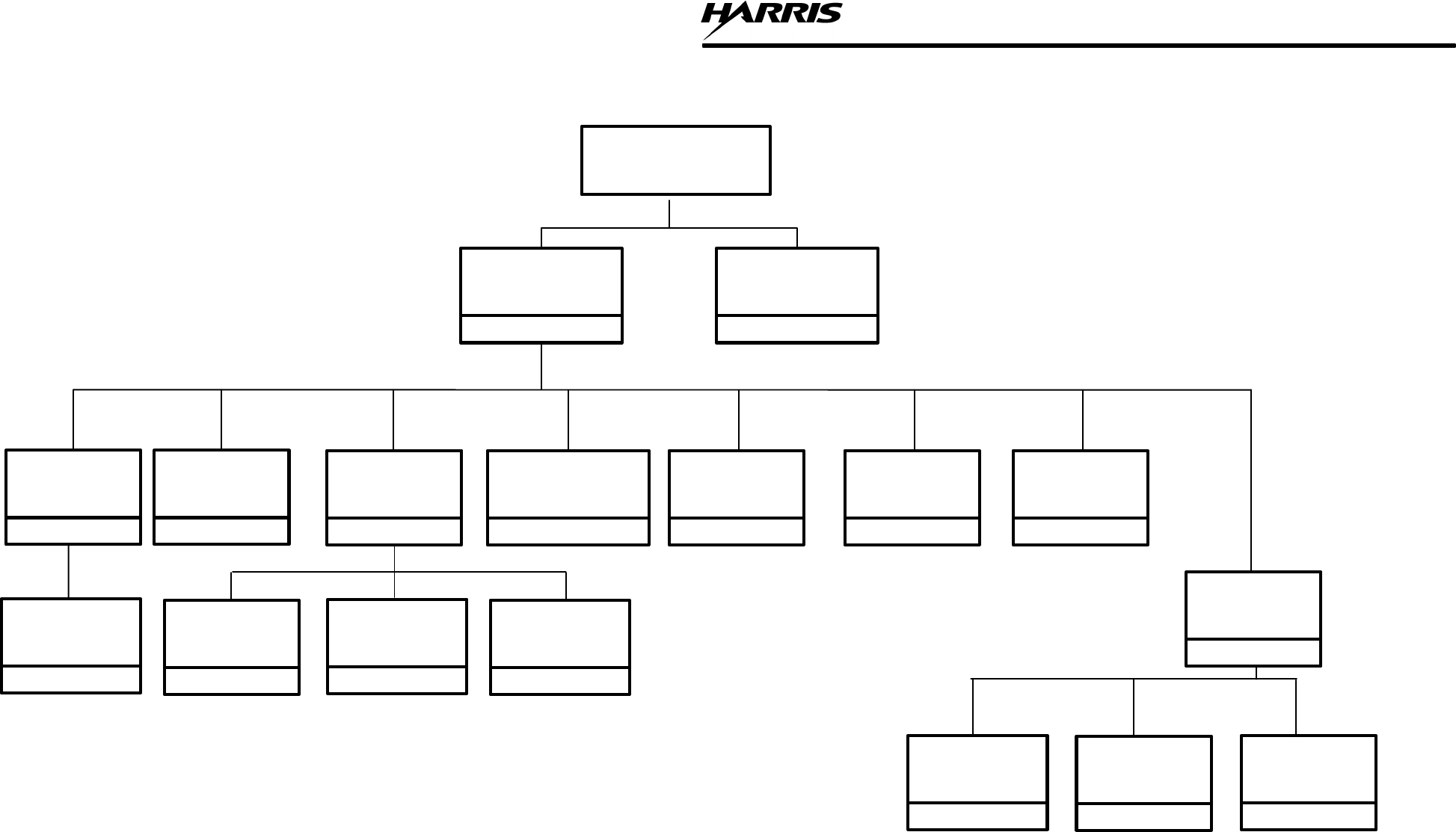
MX-9325
SUPPORT DATA
7-5/7-6
A2
DIGITAL PWB
ASSEMBLY
12007-2500
A3
EXCITER PWB
ASSEMBLY
A4
HEATSINK
ASSEMBLY
A4A1
POWER AMPLIFIER
ASSEMBLY
A4A2
28 VDC POWER
SUPPLY
ASSEMBLY
02-6014A01
MX-9325
MULTIMODE TRANSCEIVER
12007-3000 12007–4000
12007-4100
A5
LOW PASS FILTER
&
DIRECTIONAL COUPLER
ASSEMBLY
12007–4200
SOFTWARE
TBD
Figure 7-1. Tranceiver Family Tree
A4A3
REAR PANEL
CONNECTOR HUSING
ASSEMBLY
04–5133A03
A6
LOW VOLTAGE
POWER SUPPLY
ASSEMBLY
12007–4600
A7
RECEIVER PWB
ASSEMBLY
12007–5000
EIA–530
MODEM
A8
HELICAL FILTER
ASSEMBLY
12007–5600
OPTIONAL
EXTENDER UNIT
12007–6000
CHASSIS ANCILLARY KIT
RS-232
MODEM
12007–6150
DISCRETE I/O
ASSEMBLY
12007–6100
12007–6050
9325-018
12007–1000 12007–0005–01
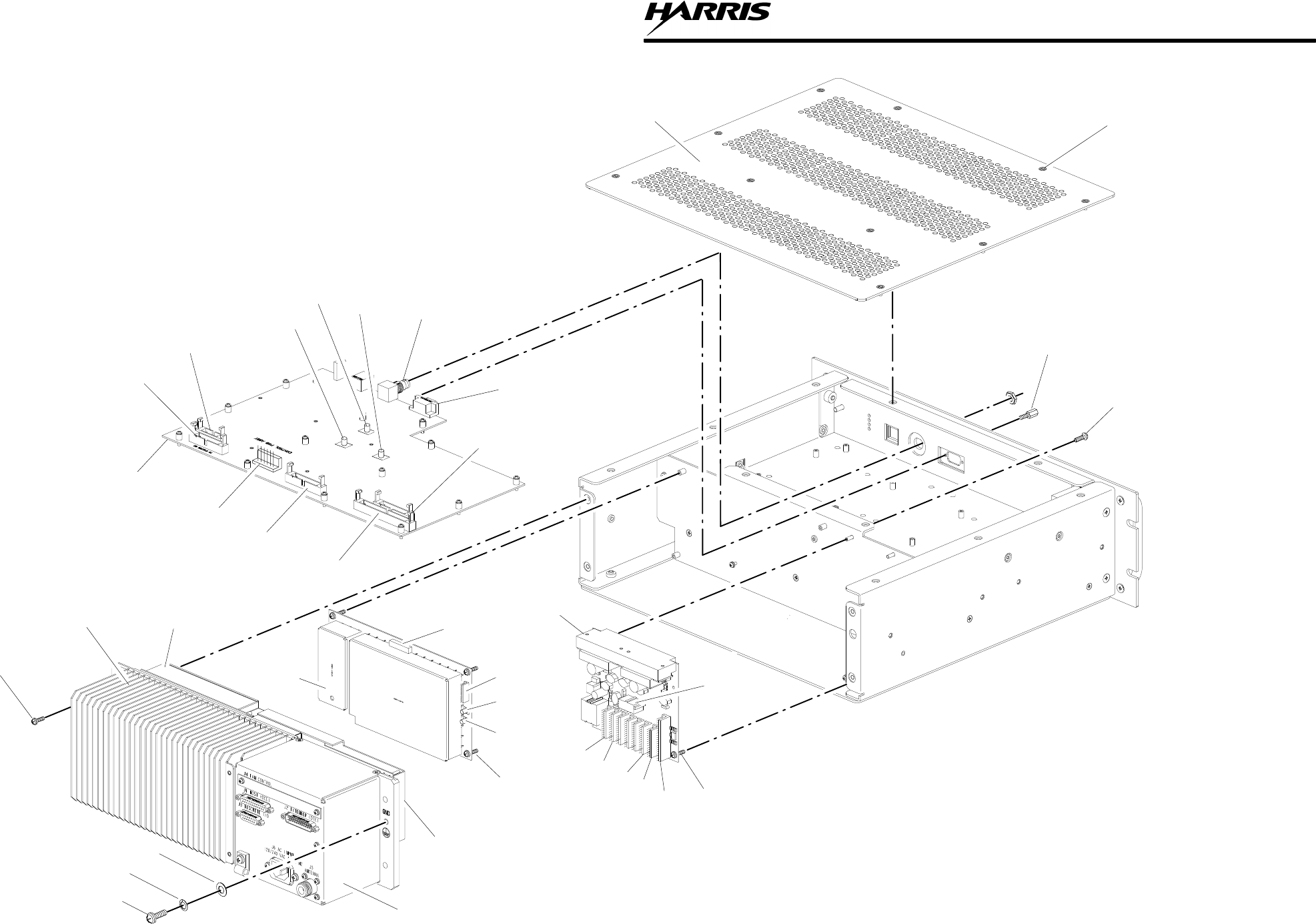
MX-9325
SUPPORT DATA
7-7/7-8
A4
Figure 7-2. MX-9325 Transceiver
Illustrated Parts List
(Sheet 1 of 2)
9325–019
J21
J18 J22
A1A2J16
A1A2J20
A1A2
ASSEMBLY
A1A2J12
A1A2J28
A1A2J30
A1A2J11
CAPTIVE
SCREWS
(2 PLACES)
D
(4 PLACES)
A1A4
ASSEMBLY
F
(2 PLACES)
E
(2 PLACES)
CAPTIVE SCREWS
(10 PLACES)
(MP1)
TOP
COVER
A1A6
ASSEMBLY
A1A5
ASSEMBLY
FRONT PANEL
REFERENCE
CONNECTOR
FRONT PANEL
MAINTENANCE
PORT
A1A4A1
A1A4A2
C
B
A A1A4A3
CAPTIVE
SCREWS
(4 PLACES)
J1
J5 J9 J8 J7 J4
A1A5J6
A1A5J3
A1A5J1
A1A5J5
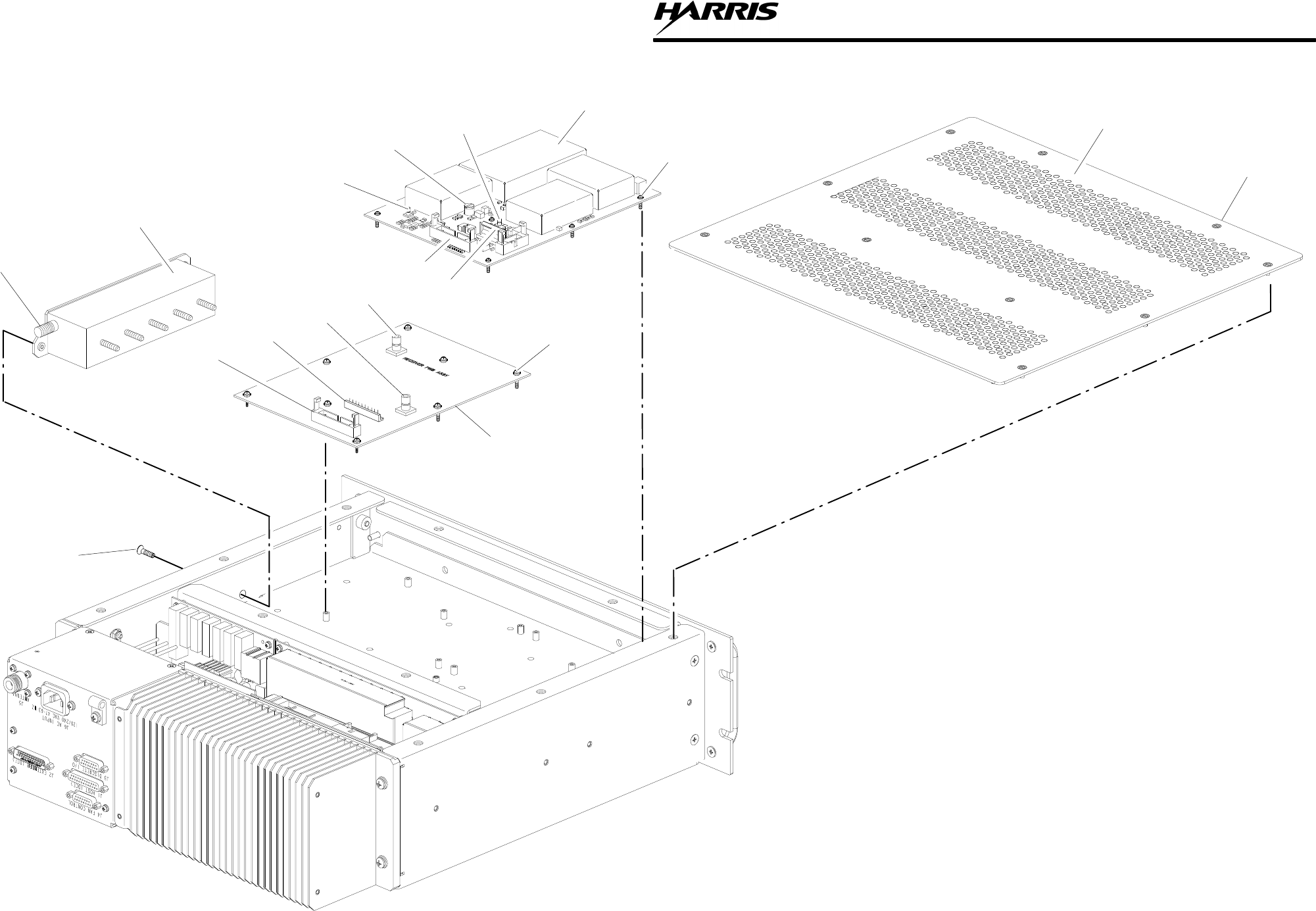
MX-9325
SUPPORT DATA
7-9/7-10
A4
Figure 7-2. MX-9325 Transceiver
Illustrated Parts List
(Sheet 2 of 2)
A1A8
ASSEMBLY
(MP2)
BOTTOM
COVER
CAPTIVE SCREWS
(10 PLACES)
G
(2 PLACES)
CAPTIVE
SCREWS
(8 PLACES)
A1A7
ASSEMBLY
A1A3
ASSEMBLY
CAPTIVE SCREW
(2 PLACES)
A1A3J3
A1A3J4
A1A3J2
A1A3J1
RF CONNECTOR
(BOTH SIDES)
A1A7J6
A1A7J5
A1A7J4
A1A7J3
CAPTIVE
SCREWS
(8 PLACES)
9325–020
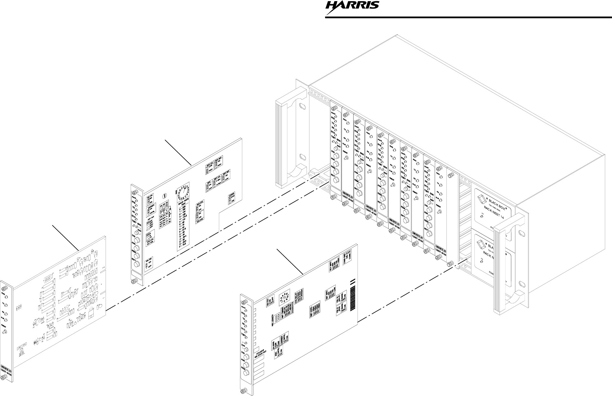
MX-9325
SUPPORT DATA
7-11/7-12
Figure 7-3. VHF Extender Unit
Illustrated Parts List
EIA–530
MODEM CARD
DISCRETE I/O
CARD
RS–232
MODEM CARD
9325-021
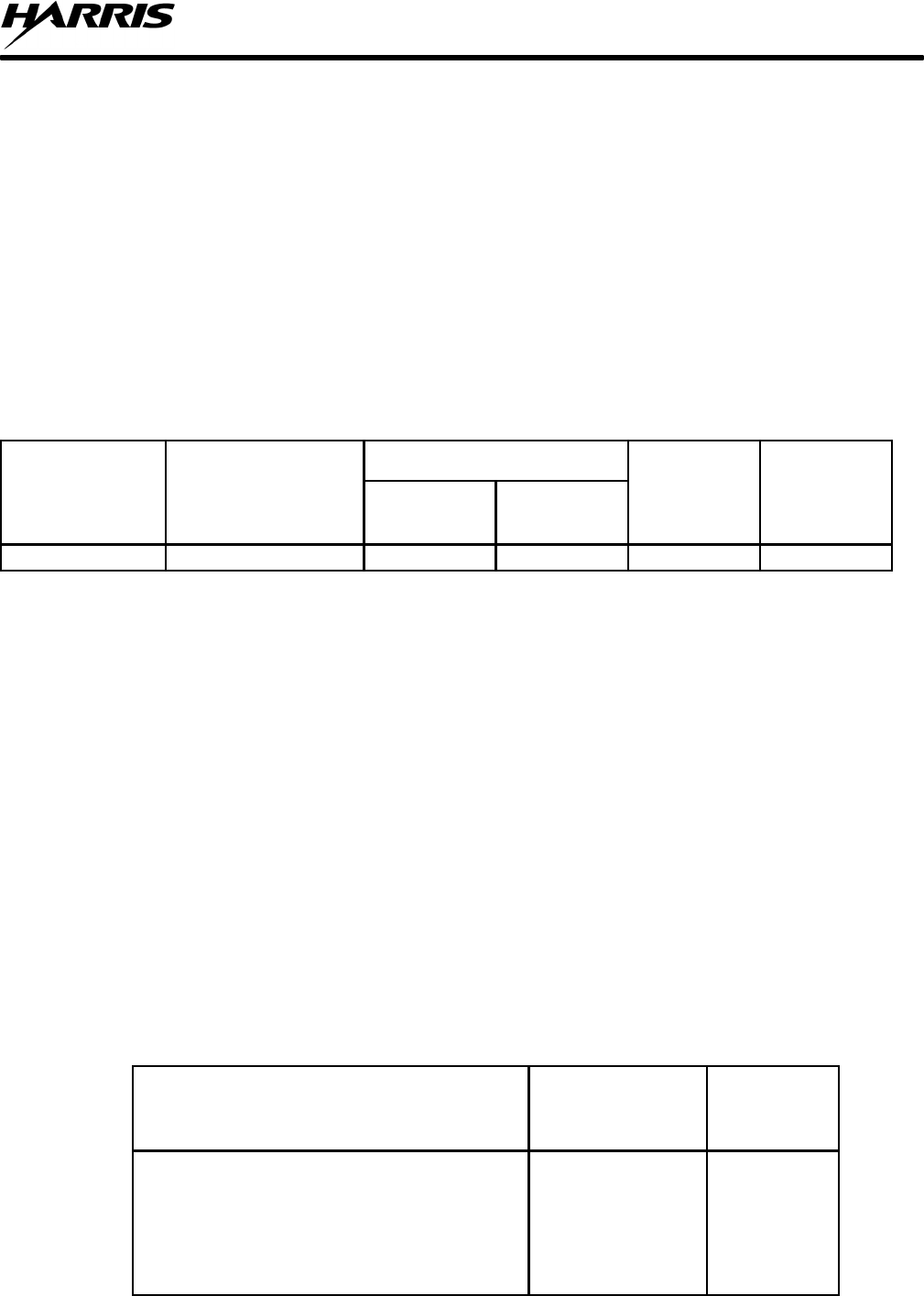
MX-9325
SUPPORT DATA
7-13
7.5 ASSEMBLY COMPONENT LOCATION REFERENCES
The following provides component locations that are referenced during fault isolation and maintenance. If the
connectors and pins are labeled on an assembly, and there are no other components referenced, then there is no
figure for that assembly. Figure 7-4 provides reference to assembly locations of A4 HeatSink Assembly.
7.6 FAULT ISOLATION INDEXES
The following provides indexes that are helpful during fault isolation. These indexes consist of a protective device
index and fault isolation index. the indexes are described in their respective paragraphs.
7.6.1 Protective Device Index
A protective device index provides information on protective devices such as circuit breakers and fuses. Table 7-7
provides the protective device index for the MX-9325 Transceiver.
Table 7-7. Protective Device Index
Rating
Reference
Designation Panel Marking
or ID Volts Amps Circuit
Protected Diag.
Ref.
CB1 AC Power 230 8 Amps AC Input 2-1, 7-2
7.6.2 Fault Isolation Index
Table 7-8 is the fault isolation index for the MX-9325 Transceiver. It is nearly impossible to identify and publish
procedures for every fault that may, or may not, occur with a particular product. To help isolate faults that are not
listed in Chapter 5, Paragraphs 5.2.2 and 5.2.3. The functional areas are listed in the left column of the index in
Table 7-8. The second column references the functional block diagrams for each functional area. A reference for
the text description for each functional area is provided in column three. Before using the index, consider the
following:
a. Is the problem in the Data signal paths? Examples may be boot errors, software errors etc.
b. Is the problem in the Transmit Signal Paths? Examples may be low power output, poor over-the-air data
transfers etc.
c. Is the problem in the Receive Signal Paths? Examples may be, poor received data quality etc.
d. Is the problem in the control signal paths? Examples may be loss of PA control, loss of remote control,
loss of front panel control, poor over-the-air data transfers etc.
e. Is the problem in the power distribution between the various assemblies? Examples could be any of those
listed for Data, Transmit, Receive or control.
Table 7-8. Fault Isolation Index
Functional Area Signal Path
Diagram
Functional
Description
Paragraph
Data Signal Paths 4-3 4.4.2
Transmit Signal Paths 4-4 4.4.2.1
Receive Signal Paths 4-5 4.4.2.1
Control Signal Paths 4-6 4.4.5
Power Distribution Paths 4-7 4.4.7
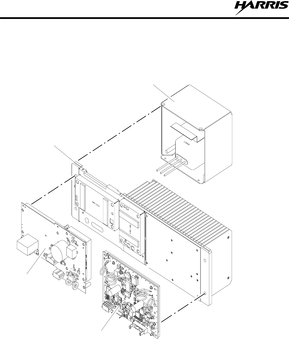
MX-9325
SUPPORT DATA
7-14
Figure 7-4. A4 Heatsink Assembly Component Location References
A4A3
A4
A4A2
A4A1 9325-022
MX-9325
SUPPORT DATA
7-15
7.7 CHASSIS CONNECTOR DATA
The following provides chassis connector data that is helpful during installation.
7.7.1 Connectors and Mating Connectors Part Numbers
Table 7-9 provides the chassis connector part numbers and their mating connector part numbers.
Table 7-9. Connectors and Mating Connectors Part Numbers
Connector Part Number Mating Connector
Part Number
TO BE DETERMINED
7.7.2 MX-9325 Transceiver Chassis Connector Pinout Data
Tables 7-10 through 7-12 provide pinout data for the connectors mounted on the MX-9325 Transceiver chassis.
Figure 8-2 provides the pin and connector locations.
Table 7-10. J1 Host Interface Port
Pin Name
1 SHIELD
2 DCE_TX_DATA_A
3 DCE_RX_DATA_A
4 DCE_RTS_A
5 DCE_CTS_A
6 DCE_DSR_A
7SIGNAL COMMON
8 DCE_DCD_A
9 DCE_RX_CLK_B
10 DCE_DCD_B
11 N/A
12 DCE_TX_CLK_B
13 DCE_CTS_B
14 DCE_TX_DATA_B
15 DCE_TX_CLK_A
16 DCE_RX_DATA_B
17 DCE_RX_CLK_A
18 N/A
19 DCE_RTS B
20 N/A
21 N/A
22 DCE_DSR B
23 N/A
MX-9325
SUPPORT DATA
7-16
Table 7-10. J1 Host Interface Port - Continued
Pin Name
24 N/A
25 N/A
Table 7-11. J2 Extender Port
Pin Name
1 SHIELD
2 DTE_TX_A
3 DTE_RX_A
4 DTE_RTS_A
5 DTE_CTS_A
6 DTE_DSR_A
7SIGNAL COMMON
8 DTE_DCD_B
9 DTE_RX_CLK_B
10 DTE_DCD_B
11 N/A
12 DTE_TX_CLK_B
13 DTE_CTS_B
14 DTE_TX_DATA_B
15 DTE_TX_CLK_A
16 DTE_RX_DATA_B
17 DTE_RX_CLK_A
18 DTE_LOCAL_LOOPBACK
19 DTE_RTS_B
20 DTE_DTR_A
21 DTE_REMOTE_LOOP-
BACK
22 DTE_DSR_B
23 DTE_DTR_B
24 N/A
25 N/A
Table 7-12. J3 Discrete I/O
Pin Name
1SHIELD/EARTH GROUND
2 TIME_REF_IN_A

MX-9325
SUPPORT DATA
7-17
Table 7-12. J3 Discrete I/O - Continued
Pin Name
3 TIME_REF_IN_B
4 TIME_REF_OUT_A
5 TIME_REF_OUT_B
6 CHAN_BUSY_IN_A
7 CHAN_BUSY_IN_B
8 CHAN_BUSY_OUT_A
9 CHAN_BUSY_OUT_B
10 RX_MUTE_IN_A
11 RX_MUTE_IN_B
12 RX_MUTE_OUT_A
13 RX_MUTE_OUT_B
14 KEY INHIBIT
15 SIGNAL COMMON
7.7.3 VHF Extender Unit Chassis Connector Pinout Data
Tables 7-13 through 7-15 provide pinout data for the connectors mounted on the MX-9325 Transceiver chassis.
Figure 8-3 provides the pin and connector locations.
Table 7-13. EIA-Modem Connections
Signal Description
(Circuit Mnemonic) Circuit Board
Edge Connector
EIA-530
Data Port
(Card Cage
DB-25 Female)
Wire Line (Card
Cage
Terminal Block)
Chassis Ground (Shield) 17, 18, 39, 40 1 1
Local Analog Loopback (LL) 10 18 –
TX Data A (BA) 14 2 –
TX Data B (BA) 37 14 –
RX Data A (BB) 35 3 –
RX Data B (BB) 36 16 –
RTS A (CA) 34 4 –
RTS B (CA) 12 19 –
CTS A (CB) 33 5 –
CTS B (CB) 24 13 –
DSR A (CC) 32 6 –
DSR B (CC) 5 22 –
Signal Ground (AB) 9, 31 7–
Remote Loopback (RL) 29 21 –
Carrier Detect A (CF) 8 8 –

MX-9325
SUPPORT DATA
7-18
Table 7-13. EIA-Modem Connections - Continued
Signal Description
(Circuit Mnemonic) Circuit Board
Edge Connector
EIA-530
Data Port
(Card Cage
DB-25 Female)
Wire Line (Card
Cage
Terminal Block)
Carrier Detect B (CF) 15 10 –
Serial Clock RX A (DD) 11 17 –
Serial Clock RX B (DD) 16 9 –
Serial Clock TX–External/DTE A (DA) 7 24 –
Serial Clock TX–External/DTE B (DA) 38 11 –
Serial Clock TX–Internal/DCE A (DB) 13 15 –
Serial Clock TX–Internal/DCE B (DB) 2 12 –
DTR A (CD) 30 20 –
DTR B (CD) 27 23 –
Test Mode Indicator (TM) 6 25 –
RX Line (–) 20 –2
RX Line (+) 42 –3
TX Line (–) 22 –4
TX Line (+) 44 –5
The pinout convention for the EIA-530 modem card edge connector is as follows:
•Facing the component side of the PWB with the card edge connector to the right, pin 1 is located at the
bottom and pin 22 is at the top.
•Facing the wire side of the PWB with the card edge connector to the left, pin 23 is at the bottom and pin
44 is at the top.
•Note that the keying slot is also counted as a “pin”.
Table 7-14. Discrete I/O Card Connections
REF CARD CAGE PINOUTS
Signal Description Card Edge
Connector
(Discrete I/O
Card)
Card Edge
Connector
(Motherboard)
Discrete I/O In-
terface To
MX-9325
Transceiver
(Card Cage
DB-25 Female)
Wireline
(or Loop)
Interface
(Card Cage
Terminal
Block)
RS-422 (–) TX P2–10 32 6
RS-422 (+) TX P1–5 5 22
RS-422 (–) RX P2–12 34 17
RS-422 (+) RX P1–16 16 9

MX-9325
SUPPORT DATA
7-19
Table 7-14. Discrete I/O Card Connections - Continued
REF CARD CAGE PINOUTS
Signal Description Card Edge
Connector
(Discrete I/O
Card)
Card Edge
Connector
(Motherboard)
Discrete I/O In-
terface To
MX-9325
Transceiver
(Card Cage
DB-25 Female)
Wireline
(or Loop)
Interface
(Card Cage
Terminal
Block)
+17 VDC P1–1, P2–11, 23
– 17 VDC P1–3, P2–33, 25
GND (SIGNAL) P1–9, P2–99, 31 7
GND (FRAME) P1–17, P1–18,
P2–17, P2–18 17, 18, 39, 40 1 1
LOOP (–) TX P1–22 22 4
LOOP (+) TX P2–22 44 5
LOOP (–) RX P2–20 20 2
LOOP (+) RX P2–20 42 3
ALARM (+) P1–7 7 24
ALARM (–) P1–6 6 25
ALARM RESET P1–2 2 12
RESERVED P1–11 33 5
RESERVED P1–2 24 13
The pinout convention for the Discrete I/O PWB card edge connector is as follows:
•Facing the component side of the PWB with the card edge connector to the right, pin P1-1 is located at
the bottom and pin P1-22 is at the top.
•Facing the wire side of the PWB with the card edge connector to the left, pin P2-1 is at the bottom and
pin P2-22 is at the top.
•Note that the keying slots are also counted as “pins”.
The pin convention for the Motherboard connector is the same as that of the EIA-530 modem.

MX-9325
SUPPORT DATA
7-20
Table 7-15. RS-232 Modem Connections
REF CARD CAGE PINOUTS
Signal Description CIRCUIT BOARD
EDGE CONNECTOR
(PWB AND
MOTHERBOARD)
RS–232
DATA PORT
DB-25 (Female)
WIRE LINE
(CARD CAGE
TERMINAL
BLOCK)
Chassis Ground 17, 18, 39, 40 1 1
Local Loopback (V.54, Loop 3) 10 18 –
TX Data 14 2 –
37 14 –
RX Data 35 3 –
36 16 –
RTS 34 4 –
12 19 –
CTS 33 5 –
24 13 –
DSR 32 6 –
5 22 –
Signal Ground 9, 31 7–
Remote Loopback (V.54 Loop 2) 29 21 –
Carrier Detect 8 8 –
–8 VDC Output 15 10 –
RX Clock Output (Sync mode) 11 17 –
+8 VDC Output 16 9 –
TX Clock Input – External (Sync Mode) 7 24 –
38 11 –
TX Clock Output – Internal (Sync
Mode) 13 15 –
2 12 –
30 20 –
27 23 –
Test Mode Indicator 6 25 –
RX Line 20 –2
RX Line 42 –3
TX Line 22 –4
TX Line 44 –5
The pin convention for the RS-232 modem card edge connector is the same as that of the EIA-530 modem.

MX-9325
SUPPORT DATA
7-21
7.7.4 VHF Extender Unit Jumper/Dip Switch Setting
Tables 7-16 through 7-18 provides jumper setting available on the VHF Extender Unit Modem and Discrete I/O
Cards. Figures 7-6 through 7-10 provides the jumper locations.
Table 7-16. EIA-530 Modem Jumper Settings
Jumper Function Possible
Settings
J1
V54 DIS Prevents activation of remote V.54 loops Enable
Disable
J2
Carrier Selects the transmit carrier mode. When ON, transmit carrier
is constantly ON. When CNTRL, transmit carrier is ON only
when RTS is HIGH
ON
CNTRL
J3
XMT Clock Selects the transmit timing signal from either: internal clock,
external clock or receive clock and enables working in Asyn-
chronous mode.
INT
EXT
RCV
ASSY
J4
RTS-CTS Delay Selects the delay between RTS and CTS. 0 ms
9 ms
70 ms
J5 N/A
J6
SW Enable Enables activation of DIG, ANA and REM loopbacks via the
front panel push buttons. ON
OFF
J7
RLB DTE (RL) Enables Remote Loopback command from the DTE interface
(21) ENABLE
DISABLE
J8
ALB DTE (LL) Enables Analog Loopback command from the DTE interface
(18). ENABLE
DISABLE
J9
RCV Level Selects the receiver sensitivity level required LOW
HIGH
J10
RCV Imped-
ance
Selects receive line impedance. 150W
HIGH
J11
REM PWR Fail Enables the Remote Power Failure feature. (Does not apply to
EU.) ON
OFF
J12
XMT Level Selects the transmit output level to the line. 0 dBm
–6 dBm
J13
XMT Imped-
ance
Selects the transmit line impedance. 150W
LOW
J14
Chassis Ground The CON setting connects Signal Ground to Chassis Ground.
The DIS setting disconnects them. CON
DIS
MX-9325
SUPPORT DATA
7-22
Table 7-17. Discrete I/O Card DIP Switch Settings
Switch Closed Open Default
Settings
S1A
(Data Polarity) Normal Inverted Closed
S1B (Alarm) NO – Relay Closes on Alarm NC – Relay Opens on Alarm Open
S1C N/a N/a Closed
S1D Closed
Table 7-18. RS-232 Modem Jumper/DIP Switch Settings
Jumper/
Switch Function Possible
Settings
1
Data Rate Selects the data rate of the modem. 0=19.2 kbps
1=14.4k
2=9.6k
3=7.2k
4=4.8k
5=3.6k
6=2.4k
7=1.2k
2
XMT Timing For synchronous operation, determines whether the transmit
timing signal comes from the internal clock, external clock or
receive clock. Select ASY for asynchronous operation.
INT
ASY
EX
RCV
3
2W/4W Selects the line output configuration of the modem 2W or 4 W. 2W
4W
4
CTS Delay Selects the RTS to CTS delay. 0ms
8ms
64ms
5
Carrier Selects the transmit carrier mode. ON setting is for constant
carrier, the CTRL setting is used to switch the carrier on only
when RTS is high
ON
OFF
6
XMT Level Selects the transmit line level output. 0dBm
–3dBm
–6dBm
–9dBm
MX-9325
SUPPORT DATA
7-23
Table 7-18. RS-232 Modem Jumper/DIP Switch Settings - Continued
Jumper/
Switch Function Possible
Settings
7
XMT IMPD Selects the transmit line impedance (ohms). 600
300
150
LOW
8
RCV IMPD Selects the receive line impedance (ohms). 600
300
150
HIGH
9
LL Pin 18 Enables or disables the Analog Loopback (LL) from the DTE
interface pin 18. EN
DIS
10
RL Pin 21 Enables or disables the Remote Loopback (RL) from the DTE
interface pin 21. EN
DIS
11
FP Switch Enables or disables control of the DIG/ANA/REM loopback
via front panel pushbutton switches. EN
DIS
12
Ground Selects or deselects connection of signal ground to chassis
ground. CONNECT
DIS CONN
13
AGC ON selects AGC always on; CTRL selects AGC on when DCD
is on, when DCD goes off, AGC remains at last level. ON
CTRL
14
V.54 Delay ON activates V.54 delay for use in tail-end circuits (prevents
multiple loopback) OFF setting sets no delay (standard config-
uration).
ON
OFF
15
ASYNC Length S1 is not used.
S2 determines the amount of stop bit shortening for Async
mode.
S3 & S4 determine the character lengths for asynchronous op-
eration.
A length of 10 bits is the required for 8 data bits, no parity, 1
stop bit.
Refer to Table 7-19 for a complete listing of all data length set-
tings.
–
ON= 25%
OFF=12.5%
S3=ON,
S4=OFF

MX-9325
SUPPORT DATA
7-24
Table 7-19. RS-232 Modem Data Length Settings
Start
Bit Data
Bit Parity Stop Bits Total Bits
Length Switch
S3 Switch
S4
1 5 NONE 2 8 OFF OFF
1 5 ODD/EVEN 1 or 1.5 8 OFF OFF
1 5 ODD/EVEN 2 9 OFF ON
1 6 NONE 1 or 1.5 8 OFF OFF
1 6 NONE 2 9 OFF ON
1 6 ODD/EVEN 1 or 1.5 9 OFF ON
1 6 ODD/EVEN 2 10 ON OFF
1 7 NONE 1 or 1.5 9 OFF ON
1 7 NONE 2 10 ON OFF
1 7 ODD/EVEN 1 or 1.5 10 ON OFF
1 7 ODD/EVEN 2 11 ON ON
1 8 NONE 1 or 1.5 10 ON OFF
1 8 NONE 2 11 ON ON
1 8 ODD/EVEN 1 or 1.5 11 ON ON
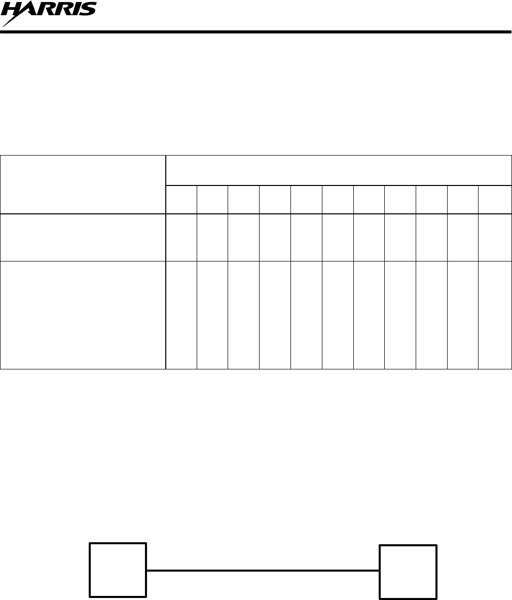
MX-9325
SUPPORT DATA
7-25
7.8 SYSTEM CABLING REQUIREMENTS
The following provides system cabling requirements and construction recommendations that is helpful during
installation. Table 7-20 lists the cabling requirements for the various site configurations. The quantities listed are
for each channel, which is equivalent to each transceiver or each TX/RX pair in the case of the Split Site
configurations.
Table 7-20. MX-9325 System Cable Requirements - Quantity per Channel
System Configuration Cable Letter Identification and Quantity per Channel
AB
#C** D E F G** H J K M*
Standard System (Local) 111 1 1
Standard System (Local)
With Antenna Switch 111 1 1 1
Remote Site Configuration 211 1 2 2 1
Remote Site Configuration
With Antenna Switch 211 1 1 1 2 2 1
Split Site Configuration 321 2 1 2 2 2 2
Split Site Configuration
with Local and Remote Antenna
Switches
321 2 2 1 1 2 2 2 2
* Cable M is optional, not required for normal system operation.
# Cable B is required for Mode 3 only (replacing Cable C or Cable G if applicable).
** Cables C and G are required for ACARS and Mode 2 only.
7.8.1 Cable Construction
The following paragraphs provide construction recommendations for each cable type. The length requirements are
determined by site rack and equipment arrangements. The typical cable consists of a single cable with 2 connector
ends, denoted P1 and P2 as shown in Figure 7-5.
Figure 7-5. Typical System Cable
P1 P2
9325-035

MX-9325
SUPPORT DATA
7-26
7.8.1.1 Cable Type “A” EIA-530 DB25 Data Cable Male/Female
This cable provides twisted pair connection for EIA–530 data between the VGC, XCVR and EU. A COTS cable
may be purchased such as Black Box Corporation EVN530–#–MF, where # is the length in feet (standard lengths
of 5, 10, 25, 50, 75, 100, 150, and 200 feet, or custom lengths available). Alternatively, a custom cable may be
constructed as described below.
The custom cable may be constructed from the material listed below:
•1 DB25 Male Connector (Crimp & Poke): AMP HDP–20 Connector Part 747554-1, Ferrule Part
1-747579-0 (Alternate Shielded Backshell Kit – with plastic cover): AMP Kit Part 747956-1
•1 DB25 Female Connector (Crimp & Poke): AMP HDP–20 Connector Part 747555-1, Ferrule Part
1-747579-0 (Alternate Shielded Backshell Kit – with plastic cover): AMP Kit Part 747955-1
•Cable – Foil shield, 12 ½ twisted pairs, plenum rated: Alpha cable 58812, 24 AWG, .294” Diameter or
similar.
Table 7-21 lists the pinout of the EIA-530 Modem cable.
Table 7-21. Type “A” EIA-530 Cable Wiring
Signal Description Connector Pin
P1 and P2
DB25 Male & Female Cable Pair
Chassis Ground (Shield) 1 1
Local Analog Loopback (LL) 18 1
TX Data A (BA) 2 2
TX Data B (BA) 14 2
RX Data A (BB) 3 3
RX Data B (BB) 16 3
RTS A (CA) 4 4
RTS B (CA) 19 4
CTS A (CB) 5 5
CTS B (CB) 13 5
DSR A (CC) 6 6
DSR B (CC) 22 6
Signal Ground (AB) 7 7
Remote Loopback (RL) 21 7
Carrier Detect A (CF) 8 8
Carrier Detect B (CF) 10 8
Serial Clock RX A (DD) 17 9
Serial Clock RX B (DD) 9 9
Serial Clock TX–External/DTE A (DA) 24 10
Serial Clock TX–External/DTE B (DA) 11 10
Serial Clock TX–Internal/DCE A (DB) 15 11
Serial Clock TX–Internal/DCE B (DB) 12 11
DTR A (CD) 20 12
DTR B (CD) 23 12
Test Mode Indicator (TM) 25 13 (single)
MX-9325
SUPPORT DATA
7-27
NOTE
The EIA-530 Modem uses RS-422 signalling convention for
most interfaces. (Exceptions are the RL, LL, and TM interfaces
which use RS-423, and the ground connections.) Each RS-422
interface involves a pair of leads labeled ”A” and ”B”. The A
lead may also be referred to as (–) and the B lead may also be
referred to as (+), which reflects the fact that, in the de-asserted
(mark) condition, B is positive with respect to A.
7.8.1.2 Cable Type “B” – Timing Cable, Custom – Standard and Remote Configuration
This cable provides twisted pair connection for the 1 pulse per 6 second (1 PP 6S) Mode 3 timing signal source
from the VGC and the Transceiver Discrete I/O connector.
The custom cable may be constructed from the material listed below:
•1 DE9 Male Connector (Crimp & Poke): Cinch Connector Part DEMA–9P Cinch Backshell Part
DMH–E–001
•DA15 Male Connector (Crimp & Poke): Cinch Connector Part DAMA–15P Cinch Backshell Part
DMH–A–001
•Cable – Foil shield, 1 twisted pair, plenum rated: Alpha cable 58902, 24 AWG, .210” Diameter or
similar.
Table 7-22 lists the pinout of the timing cable.
Table 7-22. Type “B” Timing Signal Cable Wiring
Circuit Name P1 DE9 Male P2 DA15 Male
Shield (Connect drain) 1
Time Ref In A (from VGC – PUL6–) 3 2
Time Ref In B (from VGC – PUL6+) 2 3
NOTE
The above interface uses the RS-422 signalling convention, with
leads labeled ”A” and ”B”. The A lead may also be referred to
as (–) and the B lead may also be referred to as (+), which
reflects the fact that, in the de–asserted (mark) condition, B is
positive with respect to A.
7.8.1.3 Cable Type “C” –Discrete I/O Cable, Custom – Split Site Configuration (Local)
This cable is a custom configuration, connecting the Channel Busy and Receiver Mute signals to/from the EU
Discrete I/O Card to the Transceiver (configured as a TX) Discrete I/O connector.
The custom cable may be constructed from the material listed below:
•1 DA15 Male Connector (Crimp & Poke): Cinch Connector Part DAMA-15P Cinch Backshell Part
DMH-A-001
•1 DB25 Male Connector (Crimp & Poke): Cinch Connector Part DBMA-25P Cinch Backshell Part
DMH-B-001
MX-9325
SUPPORT DATA
7-28
•Cable – Foil shield, 4 twisted pairs, plenum rated: Alpha cable 58904, 24 AWG, .221” Diameter or
similar.
•Shrink sleeve/Cable JacketingThe pinout of the cable is listed in the following table:
Table 7-23 lists the pinout of the Discrete I/O cable.
Table 7-23. Type ‘C’ – Timing and Discrete Signal Cable Wiring (Split TX)
Circuit Name Signal
Direction Transceiver
P1 DA15 Male Extender Unit
P2 DB25 Male Pair
Shield (Drain Wire) 1 1 Shield
Chan Busy In A EU → XCVR 6 4 1
Chan Busy In B EU → XCVR 7 9 1
Rx Mute Out A XCVR → EU 12 6 2
Rx Mute Out B XCVR→ EU 13 22 2
NOTE
The above interfaces use the RS–422 signalling convention, with
pairs of leads labeled ”A” and ”B”. The A lead in each case may
also be referred to as (–) and the B lead may also be referred to
as (+), which reflects the fact that, in the de–asserted (mark)
condition, B is positive with respect to A.
7.8.1.4 Cable Type “D”RG-213/214 Type Coaxial Cable, COTS
The “D” cable provides the coaxial RF connection between the XCVR and the input to the Optional Antenna
Switch, between the XCVR and the building Coaxial Lightning Protector and/or between the Optional Antenna
Switch output and the building Coaxial Lightning Protector. The cable should be constructed of RG-213/214 Low
Loss Coax Cable or similar such as Belden 9913, with Type N male connectors on each end. For reference, the RF
attenuation of the RG-213/214 type cable is approximately 2.3 dB (typical) per 100 feet at 120 MHz, and
approximately 1.5 dB per 100 feet at 120 MHz for Belden 9913. This does not include connector losses. Various
cable manufacturers carry suitable cable, such as Pasternack (mfg) part number PE3062–#, where # denotes the
length in inches, or Cable Experts 9913FCN#, where # denotes the length in feet (standard lengths of 3, 6, 50, and
100 feet, or custom lengths available).
7.8.1.5 Cable Type “E”– RS–232 DB25 Cable, COTS
Male/Female and Null Modem Adapter where applicable.
The “E“ cable provides the 25-pin RS-232 serial data connection between the VGC Antenna Control port
(RS-232 DTE – DB25 male on VGC) and the optional Null Modem Adapter (and Antenna Switch) or the
Extender Unit COTS RS–232 modem (RS-232 DCE – DB25 female on unit). The cable wiring is straight
through, 25-Pin D Male/Female cable, L-COM part number CS2N25MF–#, where # denotes the length of the
cable in feet (standard lengths of 2.5, 5, 6, 10, 12, 15, 25, and 50 feet). The Null Modem Adapter is L-COM part
number DAS25R.
7.8.1.6 Cable Type “F”– RS–232 DB25 Cable, COTS – Male/Female
The “F“ cable provides the 25-pin RS-232 serial data connection between the Extender Unit COTS RS-232
Modem (RS-232 DCE – DB25 female on unit) and the control port of the Antenna Switch. The Antenna Switch
interface is assumed to be that of the Delta Electronics MCU-8 or equivalent. Note that this interface includes a
DB25 female connector on the unit, yet adheres to a DTE pinout (signal direction) convention. The cable wiring
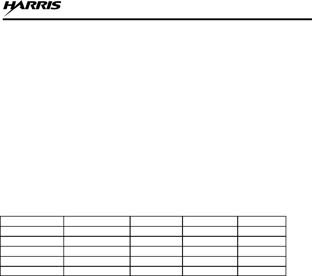
MX-9325
SUPPORT DATA
7-29
is straight through, 25 Pin D Male/Male cable, L-COM part number CS2N25MM–#, where # denotes the length
of the cable in feet (standard lengths of 2.5, 5, 6, 10, 12, 15, 25, and 50 feet).
7.8.1.7 Cable Type “G” – Discrete I/O Cable, Custom – Split Site Configuration (Remote)
This cable is a custom configuration, connecting the Channel Busy and Receiver Mute signals to/from the
Extender Unit Discrete I/O card to the Transceiver (configured as an RX) Discrete I/O connector. The cable uses
the same material as the C cable in section 5.3; however, the pinout is different.
The custom cable may be constructed from the material listed below:
•1 DA15 Male Connector (Crimp & Poke): Cinch Connector Part DAMA-15P Cinch Backshell Part
DMH-A-001
•1 DB25 Male Connector (Crimp & Poke): Cinch Connector Part DBMA-25P Cinch Backshell Part
DMH-B-001
•Cable – Foil shield, 4 twisted pairs, plenum rated: Alpha cable 58904, 24 AWG, .221” Diameter or
similar.
•Shrink sleeve/Cable Jacketing
Table 7-24 lists the pinout of the Discrete I/O cable.
Table 7-24. Type G - Discrete I/O Signal Cable Wiring (Split RX)
Circuit Name Signal Direction P1 DA15 Male P2 DB25 Male Pair
Shield (Drain Wire) 1 1 Shield
Chan Busy Out A XCVR → EU 8 6 1
Chan Busy Out B XCVR→ EU 9 22 1
Rx Mute In A EU → XCVR 10 4 2
Rx Mute In B EU → XCVR 11 9 2
NOTE
The above interfaces use the RS-422 signalling convention, with
pairs of leads labeled ”A” and ”B”. The A lead in each case may
also be referred to as (–) and the B lead may also be referred to
as (+), which reflects the fact that, in the de-asserted (mark)
condition, B is positive with respect to A.
7.8.1.8 Cable Type - H, MX-9325 and VGC Prime Power, COTS
This cable provides prime power to the MX-9325 or VGC. It is a commercial cord set suitable for 120/240 Vac.
One is supplied with each MX-9325. It is Volex part number 17518 (length 2M) or similar. An IEC60320 type
plug is fitted on the end which connects to the MX-9325 or VGC. The other end of the cable is left open (wires
only) for installation of an appropriate customer supplied plug and subsequent connection (or hardwiring) within
the customer’s rack or at a nearby wall location. Wiring conforms to the international color code of BLUE for AC
Line, BROWN for AC Neutral, and GREEN/YELLOW for Safety Ground.

MX-9325
SUPPORT DATA
7-30
7.8.1.9 Cable Type “J” – Extender Unit 115 Vac Prime Power, COTS
This cable provides 115 Vac prime power to the Extender Unit. One is supplied with each extender unit.
Approximate length is 2M. An IEC60320 type plug is fitted on the end which connects to the extender unit. A
NEMA 15 (3 prong North American) type plug is fitted on the other end which is intended for direct connection
to grounded 115 Vac power outlet within the customer’s rack or at a nearby wall location. If installed outside
North America and/or for 230 Vac operation, this cord is not used (see Cable K below).
7.8.1.10 Cable Type “K” – Extender Unit 230 Vac Prime Power, COTS
This cable provides 230Vac prime power to the Extender Unit. One is supplied with each Extender Unit.
Approximate length is 2M. An IEC60320 type plug is fitted on the end which connects to the Extender Unit. The
other end of the cable is left open (wires only) for installation of an appropriate customer supplied plug and
subsequent connection (or hardwiring) within the customer’s rack or at a nearby wall location. Wiring conforms
to the international color code of BLUE for AC Line, BROWN for AC Neutral, and GREEN/YELLOW for
Safety Ground. If the Extender Unit is installed in North America and operated on 115VAC, this cord is not used
(see Cable J above).
7.8.1.11 Cable Type “M” – RS-232 DE9 Cable Male/Female, COTS Maintenance Terminal
Connection
This cable provides the RS-232 serial data connection (temporary) between the Transceiver maintenance port and
the maintenance terminal. The cable wiring is straight through, 9 Pin D Male/Female cable, L–COM part number
CS2N9MF–6 or equivalent (standard 6 ft length recommended; other standard lengths are 2.5, 5, 10, 12, 15, 25,
and 50 feet – replace “6” with desired length).
7.8.1.12 Transmission Line - RF Coax Cable to Antennas
The ½ inch foam filled flexible transmission line is recommended for external and/or lengthy cables (e.g. 100
feet) to antennas. For reference, the RF attenuation of this type cable is approximately .23 dB (typical) per 100
feet at 120 MHz. RFS Cablewave part number 810918–001 (FLC12-50J) and N male connector part number
738802 (CONN FLC12–50NM) may be used (or Andrews equivalents). The use of a short section of flexible
cable (such as RG-213/214 as used in Cable Type D) to connect the antenna to the transmission line is
recommended for ease of installation and maintenance, and to limit mechanical stresses on the transmission line
connector due to antenna vibrations. All connector junctions exposed to the elements should be protected (e.g.
weatherproof by use of sealant and butyl tape). Installers should take care to provide adequate drip loops where
necessary, especially at building ingress/egress panels.
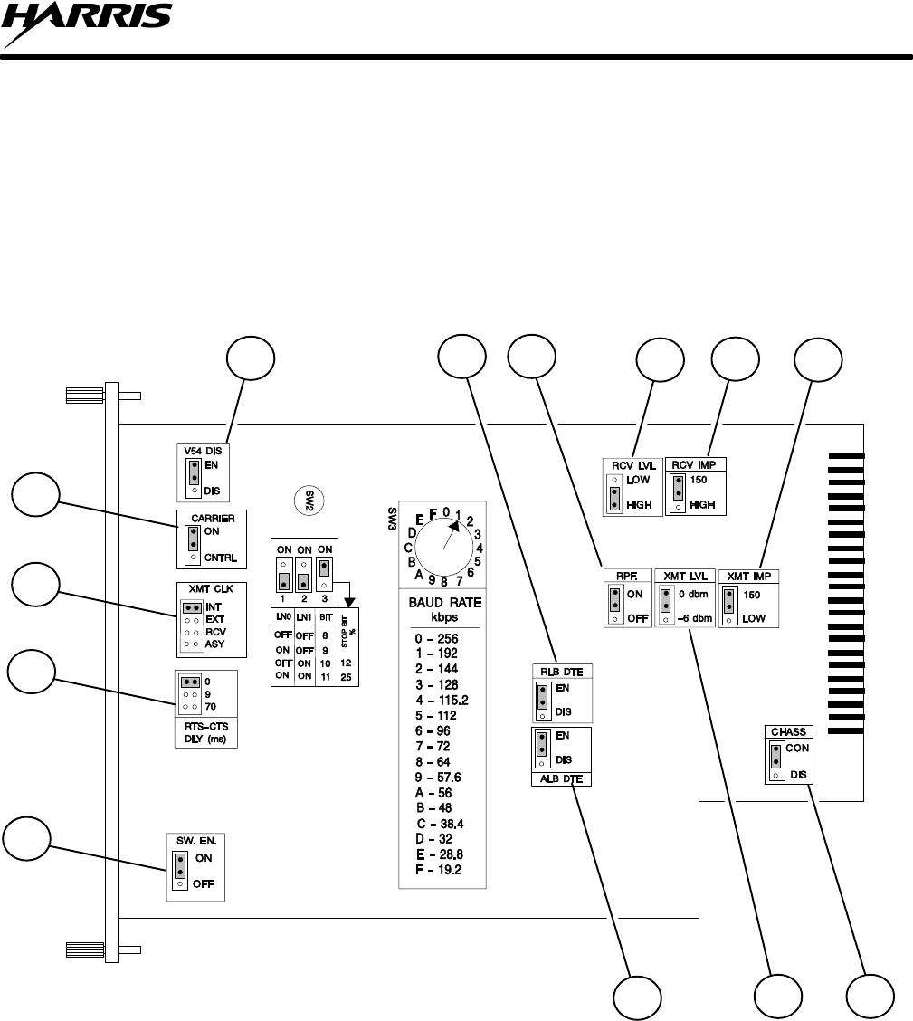
MX-9325
SUPPORT DATA
7-31
Figure 7-6. EIA-530 Modem Card
9325-023
J2
J10
J1
J3
J4
J6
J7 J11 J9 J13
J8 J12 J14
EDGE CONNECTOR
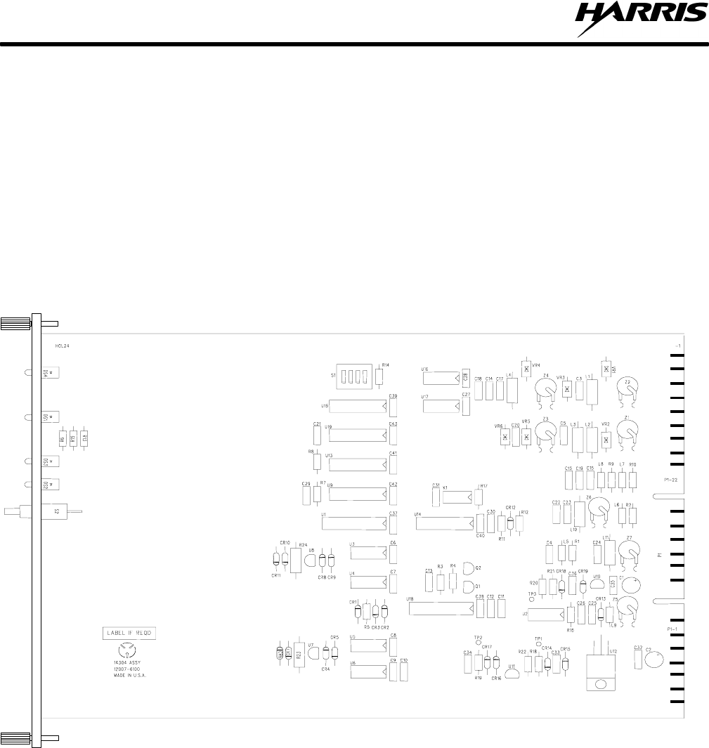
MX-9325
SUPPORT DATA
7-32
Figure 7-9. Discrete I/O Card
9325-024
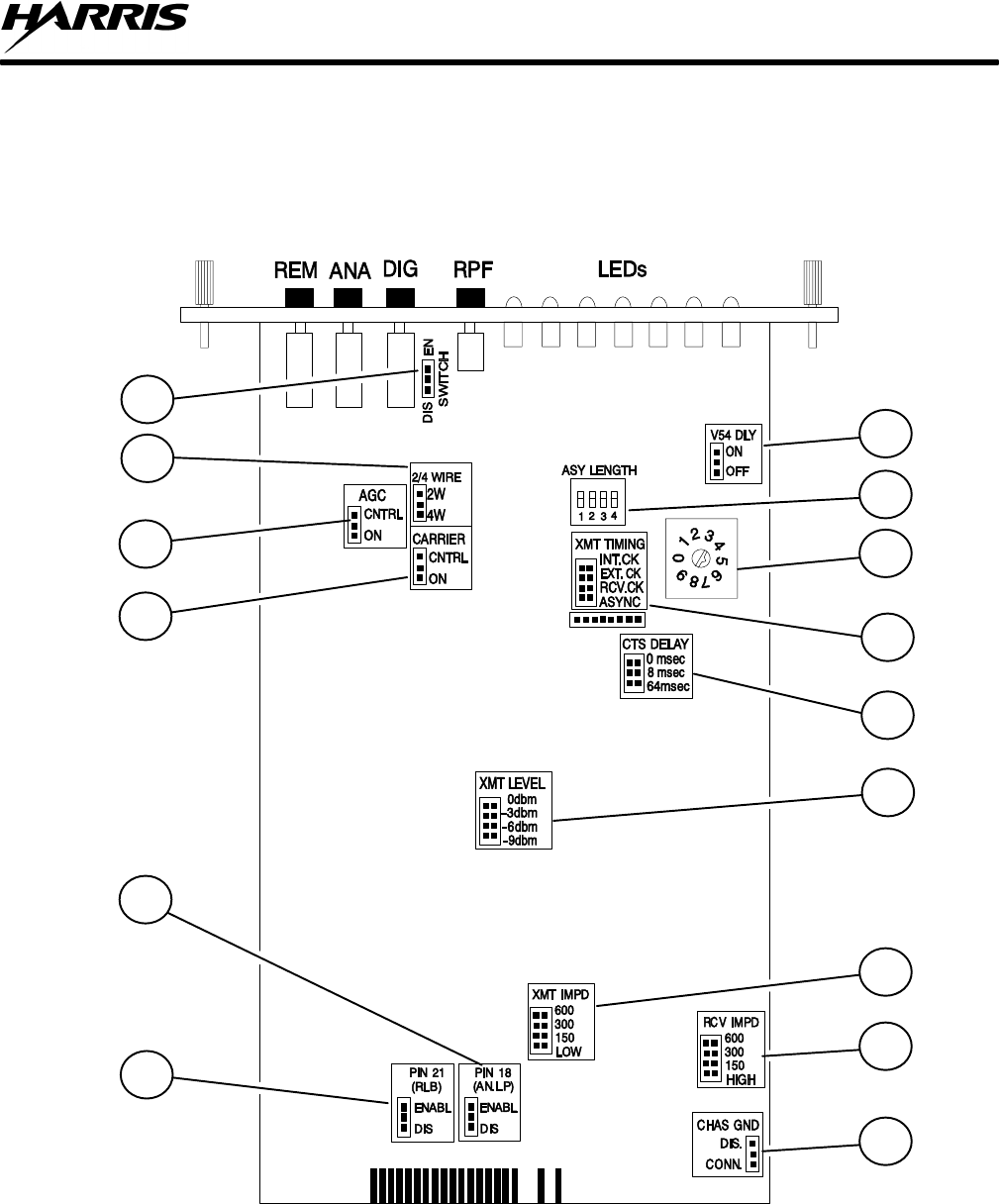
MX-9325
SUPPORT DATA
7-33
Figure 7-10. RS-232 Modem Card
9325-025
6
14
15
1
2
4
7
8
12
10
9
5
13
3
11
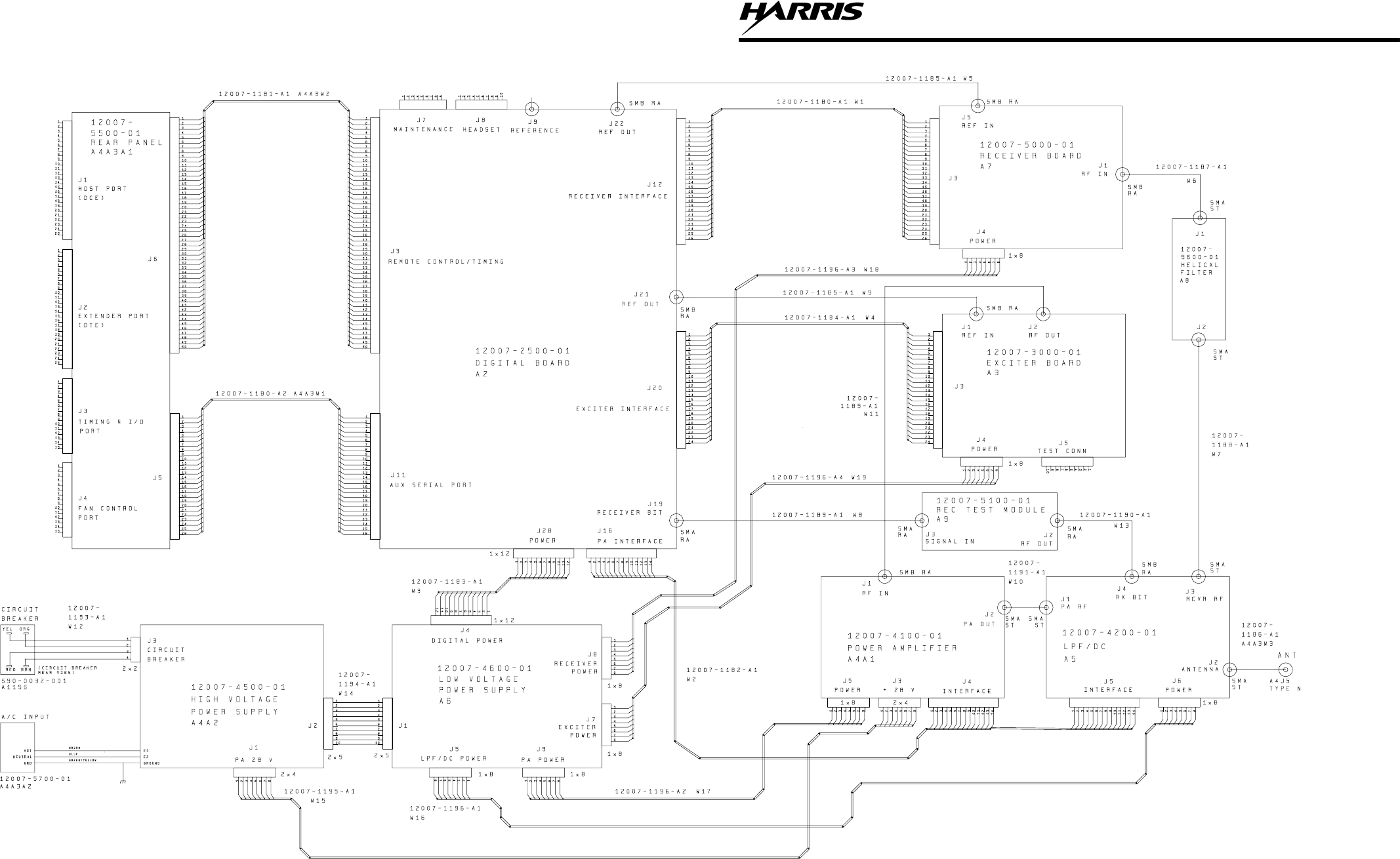
MX-9325
SUPPORT DATA
7-35/7-36
9325-026
Figure 7-11. MX-9325 Interconnect
Schematic Diagram

MX-9325
INSTALLATION
8-1
CHAPTER 8
INSTALLATION
8.1 INTRODUCTION
This chapter provides installation instructions for the MX-9325 Transceiver. Paragraph 8.2 provides
recommendations and Paragraph 8.3 provides unpacking and repacking guidelines. Paragraph 8.4 provides the
step-by-step installation procedures. Paragraph 8.5 provides post-installation procedures which consist of checks,
setup, and operational tests, all of which should be performed after installation.
8.2 INSTALLATION RECOMMENDATIONS
The information contained here provides general guidelines for installing the System. Read this chapter in its
entirety before beginning installation.
8.2.1 Selection of Physical Location
When choosing a location, become familiar with the dimensions listed in Paragraphs 8.2.2 through 8.5.3. Take
into account the following:
•Location accommodates dimensions shown on Figure 8-1.
•Room for maintenance personnel to access cabling and connectors.
•Room for proper ventilation (approximately 2 in [5.8 cm] around MX-9325 Transceiver chassis).
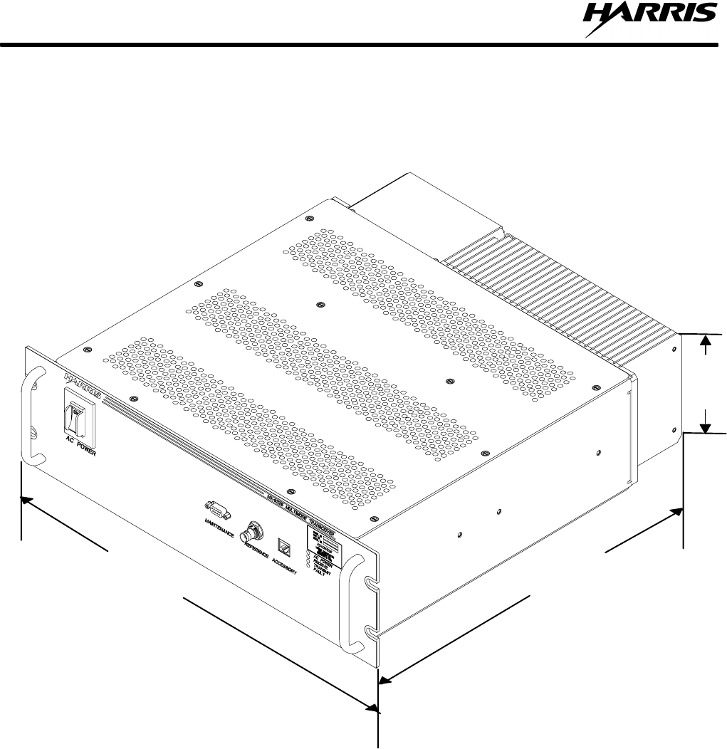
MX-9325
INSTALLATION
8-2
Figure 8-1. MX-9325 Transceiver Dimensions
9325–027
18.5”
5.25”
19”
9325-001

MX-9325
INSTALLATION
8-3
8.2.2 Grounding
When installing the MX-9325 Transceiver into a system rack, perform the following:
WARNING
Inadequate or defective grounding presents a personnel hazard
that could result in injury or death.
CAUTION
Inadequate or defective grounding could damage the equipment.
•Connect ground braid to the ground stud provided on the rear panel.
•Use as thick a braid as possible.
•Make sure braid is short (typically less than six feet [182.9 cm]).
•Connect other end of braid to TBD.
•TBD In arid climates, use ground radials.
8.2.3 Power Requirements
The MX-9325 Transceiver is designed to be powered from a 115 Vac or 230 Vac single phase source as listed in
Chapter 1, Paragraph 1.7. When the MX-9325 Transceiver is supplied as part of a system designed by Harris,
refer to the system documentation. If installing the MX-9325 Transceiver in a customer specific application, use
the supplied AC power cable listed in Chapter 7, Paragraph 7.4.4.
8.2.4 Environmental
The MX-9325 Transceiver is designed to function in the environments listed in Chapter 1, Paragraph 1.7.
8.2.5 Access Clearance and Ventilation Requirements
When the MX-9325 Transceiver is supplied as part of a system designed by Harris, refer to the system
documentation. If installing the MX-9325 Transceiver in a customer specific application, make sure there is
approximately 2-Inches (5.8 cm) around chassis.
8.2.6 Antenna Considerations
To Be Determined.
8.2.7 Tools and Materials Required
A typical installation requires standard tools listed in Chapter 7, Paragraph 7.3.

MX-9325
INSTALLATION
8-4
8.3 UNPACKING AND REPACKING
Equipment is packed in corrugated boxes. A two-piece foam enclosure protects the equipment against abrasion
and rough handling. The boxes and packing materials should be retained in case the equipment is reshipped.
The following paragraphs describe how to unpack and repack the MX-9325 Transceiver.
8.3.1 Unpacking
Perform the following procedure to unpack the equipment:
a. Inspect the exterior of the box for signs of damage during shipment. Note any problems and report them
to the proper authority. An external sticker on the shipping box provides additional instructions
concerning inspection of the package.
b. Use normal care to move the boxed equipment into the general location where it is to be installed. Certain
boxes, depending on system configuration, may be heavy. Exercise care when moving boxed assemblies
to and from locations.
c. After removing the equipment from the box, check the contents against the packing slip to see that the
shipment is complete. Report discrepancies to Harris RF Communications customer service department
(tel: 716-244-5830).
d. Save ancillary kit contents for installation in Paragraph 8.4. Parts list for kit can be found in Chapter 7,
Paragraph 7.4.4.
8.3.2 Repacking
Perform the following procedure to repack the equipment:
a. Use the original box if it was retained. If not, use a box that allows three inches of clearance on all sides
of the unit.
b. Use the original packing material if it was retained. If not, use foam packing material to fill the space
between the unit and the box. Surround the entire unit with three inches of foam packing material.
c. Use a good quality packing tape (or straps) to seal the box after closing.
8.4 INSTALLATION PROCEDURES
The following paragraphs describe the procedures performed to properly install the MX-9325 Transceiver.
NOTE
Perform the procedures in the order the paragraphs are presented
for installation. Reverse the order for MX-9325 Transceiver
removal.
MX-9325
INSTALLATION
8-5
8.4.1 Jumper/DIP Switch Settings
The following paragraphs describe the jumpers and DIP switch setting of the MX-9325 Transceiver and VHF
Extender Unit.
8.4.1.1 MX-9325 Transceiver
The MX-9325 Transceiver does not require setting of jumpers or dip-switches, however, when multiple MX-9325
Transceivers are installed in a system, their IDs need to be configured.
8.4.1.2 VHF Extender Unit
The VHF Extender Unit Modem Cards have jumper setting that need to be set depending on configuration.
Refer to Chapter 7, Paragraph 7.7.4 for jumper settings and functions.
8.4.2 Rack Mount Installation
The MX-9325 Transceiver is designed to be rack mounted on slides or brackets.
The VHF Extender Unit is designed to be rack mounted on slides or brackets.
Refer to Chapter 6, Paragraph 6.5.1 for installation procedures.
8.4.3 Stack Mount Installation
The MX-9325 Transceiver can be stack mounted as long as proper ventilation is applied between top and bottom
of equipment.
The VHF Extender Unit can be stack mounted as long as proper ventilation is applied between top and bottom of
equipment.
CAUTION
Incorrect voltage selection will damage equipment.
WARNING
Contact with line voltages will cause injury or death.
8.4.4 MX-9325 Transceiver Rear Panel Connections
Figure 8-2 shows the MX-9325 Transceiver rear panel connectors. Refer to Figures 8-4, 8-5 and 8-6 for a typical
system interconnect diagrams. Refer to Chapter 7, Paragraph 7.7 for connector data and pinout information. Refer
to Chapter 7, Paragraph 7.8 for system cabling information.
8.4.5 VHF Extender Unit Rear Panel Connections
Figure 8-3 shows the VHF Extender Unit rear panel connectors. Refer to Figures 8-4, 8-5 and 8-6 for typical
system interconnect diagrams. Refer to Chapter 7, Paragraph 7.7 for connector data and pinout information. Refer
to Chapter 7, Paragraph 7.8 for system cabling information.
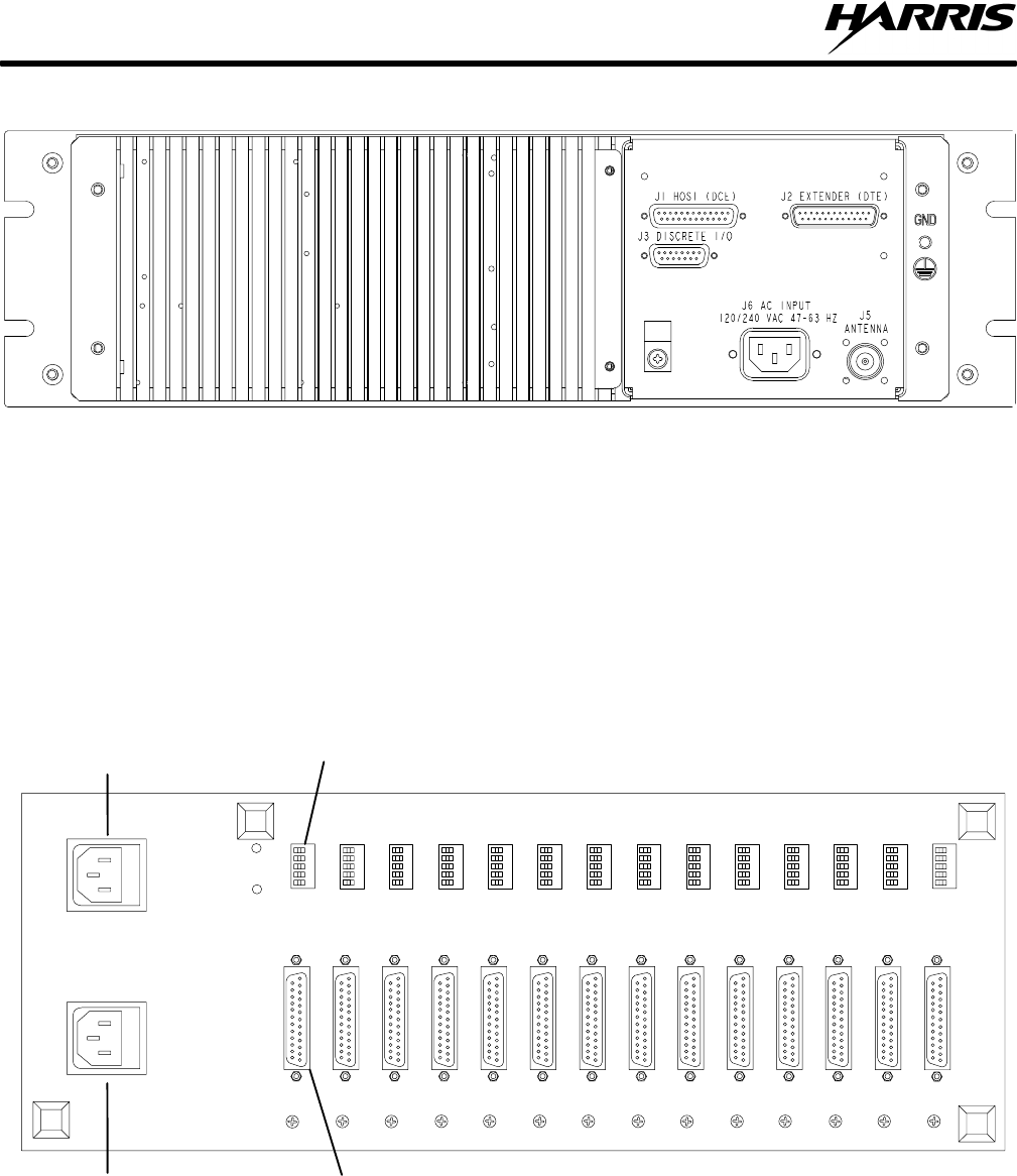
MX-9325
INSTALLATION
8-6
Figure 8-2. MX-9325 Transceiver Rear Panel Connectors
REAR VIEW 9325-028
Figure 8-3. VHF Extender Unit Rear Panel
9325-029
DB-25 CONNECTOR (14 PLACES)
TERMINAL BLOCK (14 PLACES)
115 VAC
230 VAC
8.4.6 MX-9325 Transceiver and VHF Extender Unit System Interconnects.
Figure 8-4 illustrates a typical standard site system interconnect. Figure 8-5 illustrates a typical split site system
interconnect. Figure 8-6 illustrates a typical remote site system interconnect.
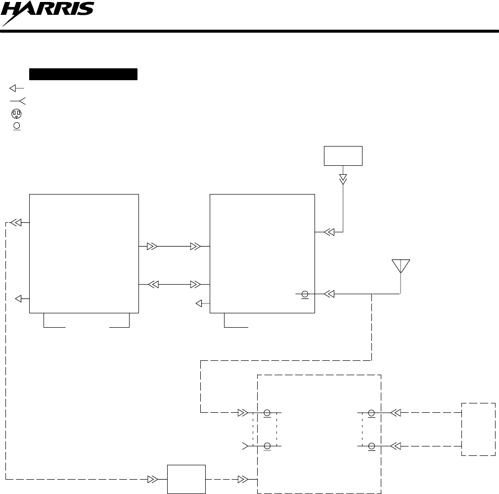
MX-9325
INSTALLATION
8-7
Figure 8-4. Typical Standard Site System Interconnect Diagram
9325-030
ANTENNA SWITCH
Antenna Switch
Control Port
(RS–232 DTE)
Antenna 1
XCVR 1
RF
MX–9325
TRANSCEIVER
Data & Maint Port
(Host)
DB25
Discrete I/O Port
DA15
Extender Unit Port
Local Maint Port DE9
Antenna I/F Type N
GROUND STATION (VGC)
Data & Maint Port
Timing Signal
Antenna Switch
Control Port–Local
(RS–232 DTE)
Antenna Switch
Control Port (Remote)
(RS–232 DTE)
Lightning
Protection
and
Antennas
(CFE)
(OPTIONAL)
Cable A
Maint.
Terminal
XCVR 8
RF Antenna 8
Type N Type N
DB25
DB25
1/2 Foamflex
Transmission Line
EIA 530
RS–422
DB 25
DE9
NOTES
CABLE A: EIA–530 DATA M/F
CABLE B: CUSTOM TIMING CABLE (REQUIRED FOR MODE 3 ONLY)
CABLE D: RG–213/214 LOW LOSS COAX
CABLE E: COTS RS–232 DATA – 25 PIN M/F
CABLE H: MX–9325 AND VGC PRIME POWER
CABLE M: COTS RS–232 DATA – 9 PIN M/F
120/240 VAC
Cable H
DE9
120/240 VAC
CABLE H
NULL
MODEM
ADAPTER
Represents a male connector (pins)
Represents a female connector (sockets)
Represents a male connector, NEMA 15 Type power plug
KEY
Cable B
Cable M
Cable E
Cable D
Represents a coax cable
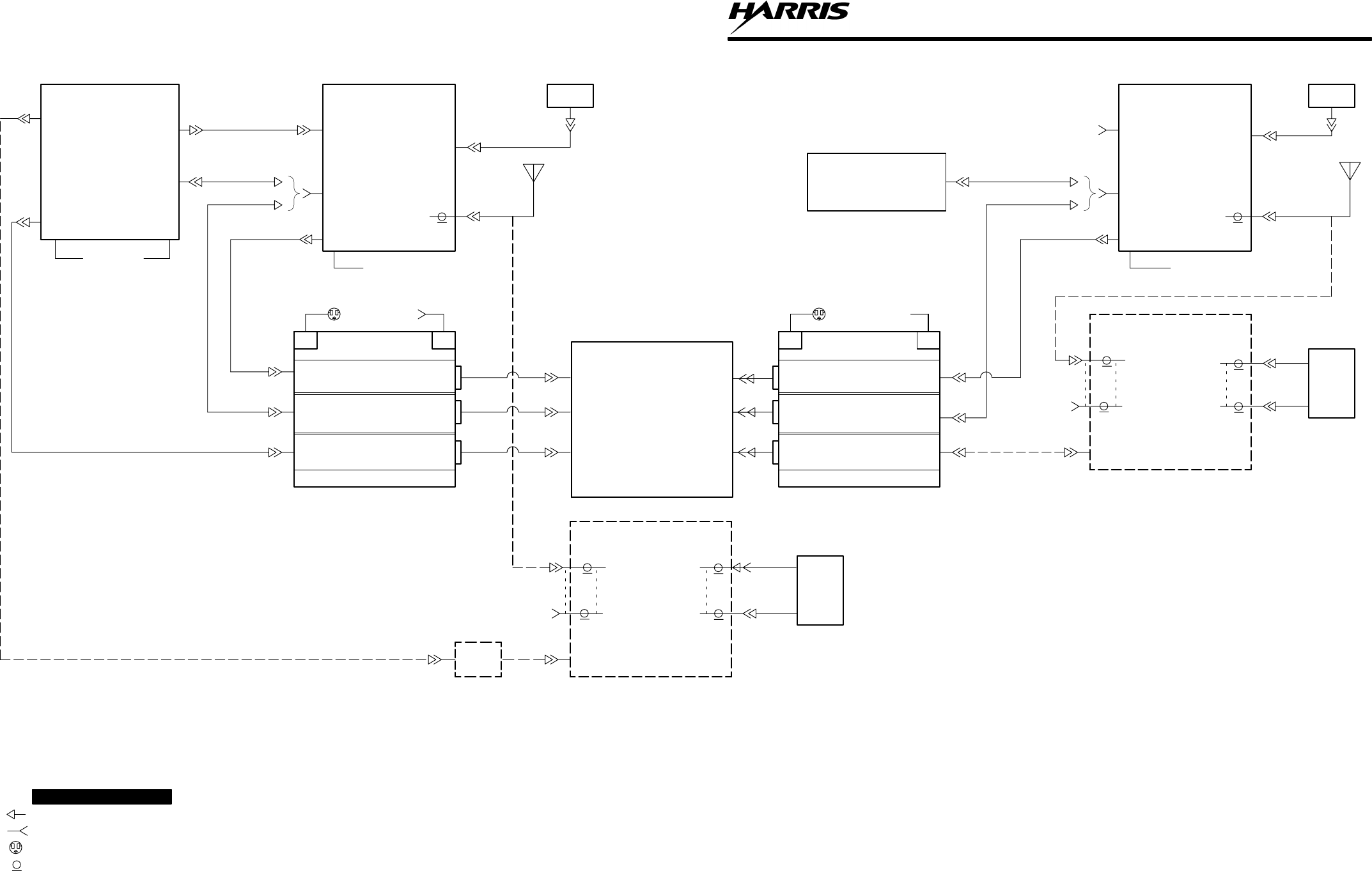
MX-9325
INSTALLATION
8-9/8-10
A4
Figure 8-5. Typical Split Site System
Interconnect Diagram
9325-031
ANTENNA SWITCH
Antenna Switch
Control Port
(RS–232 DTE)
Antenna 1
XCVR 1
RF
MX–9325
TRANSCEIVER
Data & Maint Port
(Host)
DB25
Discrete I/O Port
DA15
Extender Unit Port
Local Maint Port DE9
Antenna I/F Type N
GROUND STATION (VGC)
Data & Maint Port
Timing Signal
Antenna Switch
Control Port–Local
(RS–232 DTE)
Antenna Switch
Control Port (Remote)
(RS–232 DTE)
(OPTIONAL)
Cable A
Maint.
Terminal
XCVR 8
RF Antenna 8
Type N
DB25
DB25
EIA 530
RS–422
DB 25
DE9
120/240 VAC
Cable H
DE9
120/240 VAC
NULL
MODEM
ADAPTER
Cable B
Cable M
Cable E
Cable H
EXTENDER UNIT
PS PS
COTS EIA–530 MODEM
DISCRETE I/O CARD
(NOT REQ”D FOR MODE 3)
OPTIONAL
COTS RS–232 MODEM
DB25
DB25
DB25
Cable E
Cable A
Cable CDB25
(ACARS & Mode 2)
Cable J Cable K
115 VAC or 230 VAC
Cable D
TB
4W
TB
4W
TB
4W
ANTENNA SWITCH
Antenna Switch
Control Port
(RS–232 DTE)
Antenna 1
XCVR 1
RF
MX–9325
TRANSCEIVER
Data & Maint Port
(Host)
DB25
Discrete I/O Port
DA15
Extender Unit Port
Local Maint Port DE9
Antenna I/F Type N
TIMING SOURCE
(OPTIONAL–MODE 3 ONLY)
1PP 6S
Lightning
Protection
and
Antennas
(CFE)
(OPTIONAL)
Maint.
Terminal
XCVR 8
RF Antenna 8
Type N
DB25
120/240 VAC
Cable H
DE9
Cable B
Cable M
Cable F
Cable A
Cable C
(ACARS & Mode 2)
Cable D
EXTENDER UNIT
PS PS
COTS EIA–530 MODEM
DISCRETE I/O CARD
(NOT REQ”D FOR MODE 3)
OPTIONAL
COTS RS–232 MODEM
Cable J Cable K
115 VAC or 230 VAC
TB
4W
TB
4W
TB
4W
DB25
(Mode 3)
or
Coax
Type N
Coax
DB25
DB25
DB25
REMOTE SITE
Coax
Type N
Coax
LOCAL SITE
NOTES
CABLE A: EIA–530 DATA – 25 PIN M/F
CABLE B: CUSTOM TIMING SIGNAL CABLE (REQUIRED FOR MODE 3)
CABLE C: CUSTOM TIMING AND SIGNAL CABLE (REQUIRED FOR ACARS & MODE 2)
CABLE D: RG–213/214 COAX
CABLE E: COTS RS–232 DATA – 25 PIN M/F
CABLE H: MX–9325 AND VGC PRIME POWER
CABLE J: EXTENDER UNIT PRIME POWER – 115 VAC
CABLE K: EXTENDER UNIT PRIME POWER – 230 VAC
CABLE M: RS–232 DATA – 9 PIN M/F
CABLE F: COTS RS–232 DATA – 25 PIN M/M
CABLE G: CUSTOM DISCRETE I/O SIGNAL CABLE (REQUIRED FOR ACARS & MODE 2)
INTERSITE
CABLE
(CFE)
(MODE 3)
Lightning
Protection
(CFE)
Antennas
and
Represents a male connector (pins)
Represents a female connector (sockets)
Represents a male connector, NEMA 15 Type power plug
KEY
Represents a coax cable
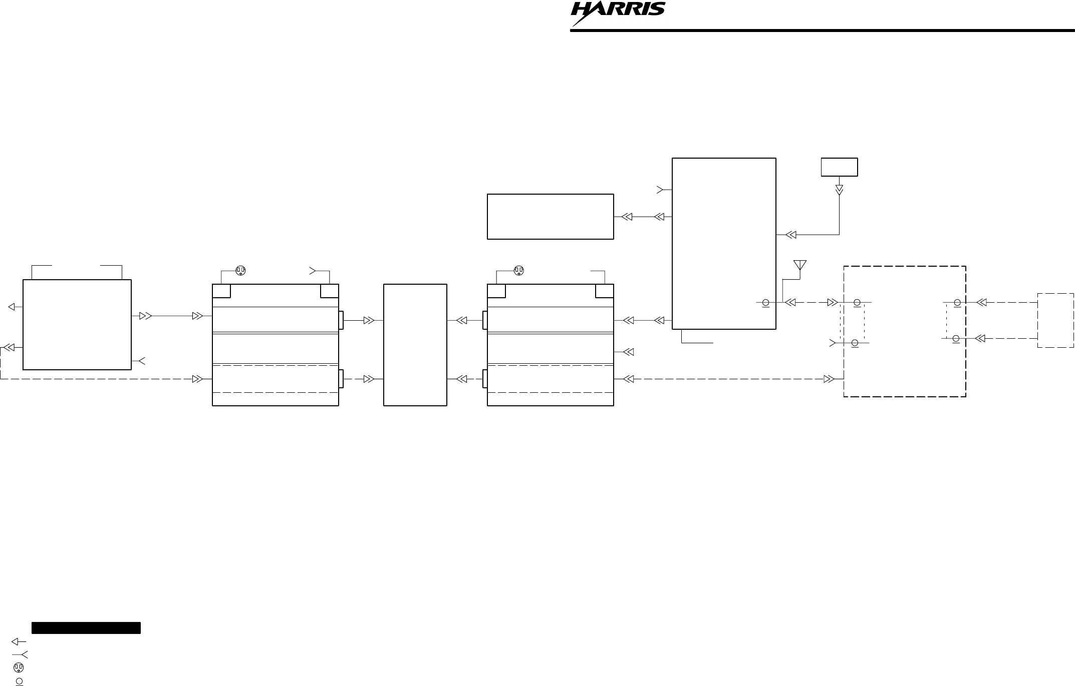
MX-9325
INSTALLATION
8-11/8-12
A4
Figure 8-6. Typical Remote Site System
Interconnect Diagram
9325-032
GROUND STATION (VGC)
Data & Maint Port
Timing Signal
Antenna Switch
Control Port–Local
(RS–232 DTE)
Antenna Switch
Control Port (Remote)
(RS–232 DTE)
Cable A
EIA 530
DB 25
120/240 VAC
Represents a male connector (pins)
Represents a female connector (sockets)
Represents a male connector, NEMA 15 Type power plug
KEY
Cable H
EXTENDER UNIT
PS PS
COTS EIA–530 MODEM
OPTIONAL
COTS RS–232 MODEM
DB25
DB25
Cable E
DB25
Cable J Cable K
115 VAC or 230 VAC
TB
4W
TB
4W
ANTENNA SWITCH
Antenna Switch
Control Port
(RS–232 DTE)
Antenna 1
XCVR 1
RF
MX–9325
TRANSCEIVER
Data & Maint Port
(Host)
Discrete I/O Port
DA15
Extender Unit Port
Local Maint Port DE9
Antenna I/F
TIMMING SOURCE
(OPTIONAL–MODE 3 ONLY)
1PP 6S
Lightning
Protection
and
Antennas
(CFE)
(OPTIONAL)
Maint.
Terminal
XCVR 8
RF
Antenna 8
Type N
DB25
120/240 VAC
Cable H
DE9
Cable B
Cable M
Cable F
Cable A
Cable D
INTERSITE
CABLE
(CFE)
EXTENDER UNIT
PS PS
COTS EIA–530 MODEM
OPTIONAL
COTS RS–232 MODEM
Cable J Cable K
115 VAC or 230 VAC
TB
4W
TB
4W
DB25 Type N
DB25
DB25
DB25
REMOTE SITE
NOTES
CABLE A: EIA–530 DATA – 25 PIN M/F
CABLE B: CUSTOM TIMING CABLE (REQUIRED FOR MODE 3 ONLY)
CABLE D: RG–213/214 LOW LOSS COAX
CABLE E: COTS RS–232 DATA – 25 PIN M/F
CABLE F: COTS RS–232 DATA – 25 PIN M/M
CABLE H: MX–9325 AND VGC PRIME POWER
CABLE J: EXTENDER UNIT PRIME POWER –115 VAC
CABLE K: EXTENDER UNIT PRIME POWER –230 VAC
CABLE M: COTS RS–232 DATA – 9 PIN M/F
1/2 Foarm Flex
LOCAL SITE
Represents a coax cable

MX-9325
INSTALLATION
8-13
8.5 POST-INSTALLATION PROCEDURES
8.5.1 Inspection of Installation
When the radio system is installed and all connector cables are attached, verify that the following items are
completed:
•All connectors are attached and tight.
•All associated hardware is secure.
•The equipment cannot be tipped over or moved.
8.5.2 Initial Settings and Power On
Table 8-1 lists the initial settings and power on procedures.
Table 8-1. Initial Settings and Power On Procedure
Step Observe Reference
a. Connect a 50-Ohm RF attenuator to
rear panel connector J104.
b. Place PC or terminal POWER
switch in ON position. The PC boots or terminal powers
on. Refer to PC or terminal operation
instructions.
c. If using a PC, run the desired
terminal emulation program. The PC runs the terminal
emulation program. Refer to software operation in-
structions for more information.
d. Ensure that the terminal emulation
software or terminal is correctly
configured.
Refer to Chapter 3, Paragraph
3.2.1. Also refer to terminal or
emulation software operation
instructions.
e. Place POWER switch on MX-9325
Transceiver front panel in the ON
position.
The PC or terminal displays the
power-up screen. See Figure
TBD.
If the PC or terminal does not
display the power-up screen, re-
fer to the non-BIT
troubleshooting procedures in
Paragraph 5.2.3.
f. PC or terminal keyboard, type BIT
command: bit v <enter>.If a BIT fault is displayed on the
PC or terminal as a result of the
BIT command, write down the
fault code.
Refer to the BIT troubleshooting
procedures in Paragraph 5.2.2.
If no errors occur during BIT,
continue operating the radio
system in an attempt to generate
a run-time fault. Periodically
enter the tst <enter> command
in order to force the transmitter
into running BIT.
If a run-time fault is generated,
refer to the non-BIT trouble-
shooting procedures in Paragraph
5.2.3. If a BIT fault is generated,
refer to the BIT troubleshooting
procedures in Paragraph 5.2.2.
If no fault is generated, return
radio system to operational
readiness.

MX-9325
INSTALLATION
8-14
8.5.3 Radio Check
After installing the MX-9325 Transceiver and it has passed the initial setting and power on procedure a radio
check should be preformed. A radio check consists of programing for channels, modes, and power levels that are
going to be used. Transmit and receive between two stations with identical programming/configurations. During
back-to-back tests, verify the following:
•All channels used
•All modes
•All power levels

MX-9325
GLOSSARY
A-1
APPENDIX A
GLOSSARY
A.1 GLOSSARY
The following provides a glossary of Abbreviation and Acronyms used in this manual.
List of Abbreviations and Acronyms
Abbreviation Term
A, AMP Ampere(s)
ac, AC Alternating Current
ACARS Aircraft Communications Addressing and Reporting systems
ADC Analog-to-Digital Converter
ADS Automatic Dependent Surveillance
ANSI American National Standards Institute
ANT Antenna
AOC Aeronautical Operational Control
ARTCC Air route traffic control center
ASCII American Standard Code for Information Interchange
ATC Air Traffic Control
ATCRBS Air traffic control radar beacon system
ATCT air traffic control tower
AVPAC Aviation VHF Packet communications
AUX Auxiliary
AWG American Wire Gauge
BERT Bit Error Rate Tester
BPS bits per second
BSI British Standard Institute
BIT Built-In Test
BITE Built-In Test Equipment
BW Bandwidth
CCentigrade/Celsius
CAA civil aviation authority
CARC Chemical Agent Resistive Coating
CB Circuit Breaker
CBIT Continuous Built-In Test
CCW Counterclockwise
CE European Community
cm Centimeter
CMU Communication Management Unit

MX-9325
GLOSSARY
A-2
List of Abbreviations and Acronyms – Continued
Abbreviation Term
COTS Commercial Off-the-Shelf
CPLR Coupler
CR Carriage Return
CSA Canadian Standard Association
CSMA Carrier Sense Multiple Access
D8PSK Differential 8 Phase Shift Keying
DAC Digital-to-Analog Converter
DAM Direct Access Memory
dB Decibel(s)
dBm Decibels referenced to 1 milliwatt
dc, DC Direct Current
DCD Data Carrier Detect
DCE Data Circuit Terminating Equipment
DE Data Encryption
Demod Demodulated
Diff Differential
Dip, DIP Dual In-Line Package
DMM Digital Multimeter
DP Double Pole
DPDT Double Pole, Double Throw
DPRAM Dual-Port RAM
DPST Double Pole, Single Throw
D/A Digital to Analog
DSP Digital Signal Processor
DSR Data Set Ready
DTE Data Terminal Equipment
DTL Diode Transistor Logic
DTM Data Text Message
DV Digitized Voice
DTMF Dual Tone Multi-Frequency
DTR Data Terminal Ready
DUART Dual Universal Asynchronous Receiver-Transmitter
DUSART Dual Universal Synchronous/Asynchronous Receiver-Transmitter
DVM Digital Voltmeter
DVOM Digital Volt-Ohm Meter

MX-9325
GLOSSARY
A-3
List of Abbreviations and Acronyms – Continued
Abbreviation Term
EAM Embedded Adaptive Module
EAROM Electronically Alterable Read Only Memory
ECM Electronic Counter Measure
ECCM Electronic Counter-Counter Measure
EEPROM, E2PROM Electrically Erasable Programmable Read Only Memory
EMI Electromagnetic Interference
EIA Electronic Industries Association
EOM End of Message
EPROM Erasable Programmable Read-Only Memory
EUROCAE The European Organization for civil aviation Equipment
FAA Federal Aviation Administration
FCC Federal Communications Commission
FD Full Duplex
FEC Forward Error Correction
FET Field-Effect Transistor
F/F Flip-Flop
FFT Fast Fourier Transform
FH Frequency Hopping
FSK Frequency Shift Keying
F/W, FW Firmware
G-A, G/A Ground-to-Air
GF Government (or customer) Furnished
GFE Government-Furnished Equipment
Gnd, GND Ground
GNI Ground Network Interface
GPIB General Purpose Interface Bus
GUI Graphical User Interface
HD Half Duplex
HDCP Harris Data Communications Protocol
HDLC High-Level Data Link Control
HF High Frequency
HSS High-Speed Synchronizer
HSSB High-Speed Serial Bus
HWCI Hardware Configuration Item
Hz Hertz

MX-9325
GLOSSARY
A-4
List of Abbreviations and Acronyms – Continued
Abbreviation Term
IC Integrated Circuit
ID Identification
IDF Intermediate Distribution Frame
IF Intermediate Frequency
INT Interrupt
INTLK Interlock
INTR Interrupt
I/O Input/Output
ICAO International Civil Aviation Authority
ISB Independent Sideband
ISO International Standards Organization
JJoules
kKilo (thousand)
KBPS Kilo Bits Per Second
kbyte Kilobyte
kHz Kilohertz
km Kilometer(s)
kV Kilovolt(s)
kVA Kilovolt Ampere(s)
KVD Keyboard Visual Display
KVDU Keyboard Visual Display Unit
kW Kilowatt(s)
LAN Local Area Network
LAPB Link Access Protocol, Balanced
LBT Listen Before Transmit
LC Inductive Capacitive
LCD Liquid Crystal Display
LD Lock Detect
LED Light-Emitting Diode
LF Low Frequency
LLSB Lower Lower Sideband
LOS Line of Sight
LP Low Pass
LPC Linear Predictive Coding
LQA Link Quality Analysis

MX-9325
GLOSSARY
A-5
List of Abbreviations and Acronyms – Continued
Abbreviation Term
LRU Line Replaceable Unit
LSB Lower Sideband
LSD Least Significant Digit
MMeter, Mega (one million)
mMilli, one-one thousandth
mA Milliampere(s)
MART Multimode Aeronautical Radio System
Mbyte Megabyte
MDM MODEM
MHz Megahertz
MIC Microphone
MIL-STD Military Standard
mm Millimeter(s)
Mod Modification, Modulated
Mod/Demod Modulator/Demodulator
Modem Modulator/Demodulator
MOPS Minimum Operational Performance Standard
MOS Metal Oxide Semiconductor
MOSFET Metal Oxide Semiconductor Field Effect Transistor
ms, msec Millisecond
MSK Minimum Shift Keying
MTBCF Mean Time Between Critical Failure
MTBF Mean Time Between Failure
MTBM Mean Time Between Maintenance
MTBR Mean Time Between Replacement
MUF Maximum Usable Frequency
Mux Multiplex, Multiplexer
mVac Millivolts Alternating Current
mVdc Millivolts Direct Current
nNano (1 x 10⁻⁹)
NB Narrowband
NC, N.C. Normally Closed
N/C Not Connected
NMOS N-channel Metal-Oxide-Semiconductor
NO, N.O. Normally Open

MX-9325
GLOSSARY
A-6
List of Abbreviations and Acronyms – Continued
Abbreviation Term
No. Number
NPN N-type, P-type, N-type (transistor)
nsec Nanoseconds
NVG Night Vision Goggles
WOhms, a unit of resistance measurement
O&M Operation and Maintenance
O&R Operation and Repair
O.C. Open Circuit or Open Collector
OEM Original Equipment Manufacturer
Op Amp Operational Amplifier
OCXO Oven Controlled Crystal Oscillator
pPico
PA Power Amplifier
PBIT Periodic Built-In Test
PABX Private Automatic Branch Exchange
PCB Printed Circuit Board
PC Personal Computer
PCM Pulse Code Modulation
PEP Peak Envelope Power
pF Picofarad (1 x 10–12 Farads)
PIV Peak Inverse Voltage
PLL Phase-Locked Loop
PNP P-type, N-type, P-type (transistor)
P-P Peak-to-Peak
PPS Pulse Per Second
PROM Programmable Read Only Memory
PS Power Supply
Pt Pt, Pt-Pt Point-to-Point
PTT Push-to-Talk
PWB Printed Wiring Board
QTY Quantity
R, RG Receiver Circuit: Receive, Receive Ground (from teletype)
RAD Random Access Data
RAM Random Access Memory
RC Resistive Capacitive

MX-9325
GLOSSARY
A-7
List of Abbreviations and Acronyms – Continued
Abbreviation Term
RCU Remote Control Unit
RCV/RX Receive
RCVR Receiver
RD Read
RDY Ready
REC Receptacle
RETX Retransmit
RF Radio Frequency
RFI Radio-Frequency Interference
RLPA Rotatable Log Periodic Antenna
RLSD Receive Level Sense Detect
RMS Root Mean Squared
ROM Read-Only Memory
RST Reset
RTC Real Time Clock
RTN Return
RTS Request to Send
RTTY Radio Teletype
RTU Remote Terminal Unit
S, SG Send Circuit, Send Ground (to teletype)
SA Spectrum Analyzer
SB Sideband
SCR Silicon Controlled Rectifier
SHLD Shield
SINAD A ratio of (signal + noise + distortion) to (noise + distortion) used to measure
the signal quality of a communication channel. SINAD is commonly used to
evaluate the ability of a channel to pass voice traffic.
Sip, SIP Single In-Line Package
SMD Surface-Mount Device
SNR Signal-to-Noise Ratio
SOM Start of Message
SP Single Pole
SPDT Single-Pole, Double-Throw
SSB Single Sideband
ST Single Throw

MX-9325
GLOSSARY
A-8
List of Abbreviations and Acronyms – Continued
Abbreviation Term
SWR Standing Wave Ratio
SYNC Synchronous
TB Terminal Board
TCXO Temperature Controlled Crystal Oscillator
TDQPSK Time Differential Quaternary Phase Shift Keying
TGC Transmitter Gain Control
T/R Transmit/Receive
TT Teletype
TTL Transistor-Transistor Logic
TT VFT Teletype Voice Frequency Tone
TTY Teletype
TX Transmit
uMicro (1 x 10⁻⁶)
UART Universal Asynchronous Receiver-Transmitter
uF Microfarad (1 x 10⁻⁶ Farads)
UHF Ultra High Frequency
USART Universal Synchronous/Asynchronous Receiver-Transmitter
USB Upper Sideband
usec Microseconds
UUSB Upper Upper Sideband
UUT Unit Under Test
uW Microwave
VVolt
VA Volt-Ampere
Vac Volts, Alternating Current
VCA Voltage Controlled Attenuator
VCO Voltage Controlled Oscillator
VCTCXO Voltage Controlled Temperature Compensated Crystal Oscillator
VDC, Vdc Volts, Direct Current
VDL VHF Data Link
VDU Video Display Unit
VECT Vector
VF Voice Frequency
VFO Variable Frequency Oscillator
VFR Voice Frequency Repeater

MX-9325
GLOSSARY
A-9
List of Abbreviations and Acronyms – Continued
Abbreviation Term
VGC VHF Ground Station Computer
VHF Very High Frequency
VLF Very Low Frequency
VMOS V-groove Metal-Oxide-Semiconductor
VOM Volt-Ohm-Meter
VOX Voice Operated Transmitter
Vpp Volts peak-to-peak
VSWR Voltage Standing Wave Ratio
WWatt(s)
WRL Wire Run List
XCVR Transceiver
XMT Transmit
XMTR Transmitter

MX-9325
GLOSSARY
A-10
This page intentionally left blank.

MX-9325
MAINTENANCE LEVELS
B-1
APPENDIX B
MAINTENANCE LEVELS
B.1 MAINTENANCE LEVELS
Figure B-1 describes the Harris defined and supported maintenance levels.
MX-9325
MAINTENANCE LEVELS
B-2
HUMM,
THERE’S
SOMETHING
WRONG WITH
MY SYSTEM
PA BAD FILTER
MAINTENANCE CONCEPT OUTLINE
LEVEL I
CORRECTIVE
AND PREVENTIVE
MAINTENANCE
TECHNICAL
MANUALS
TRAINING
LEVEL II
NO SPECIAL ITEMS
NO TOOLS/TEST
EQUIPMENT
I SEE, THE
PROBLEM IS
WITH THE PA.
PA BAD FILTER
MAINTENANCE
REPAIR KITS
COMMON TOOLS
TEST EQUIPMENT
AND
SPARES
NO SPARES
OPERATOR
TRAINING
NO SPECIAL ITEMS
SYSTEMS
MANUAL
SYSTEMS
MAINTENANCE
TRAINING
LEVEL III
WELL...BIT
LEADS ME TO
SUSPECT A
FAULTY MODULE
MODULE#: A30
FAULT #: F12
UNIT
MAINTENANCE
MANUAL
UNIT
MAINTENANCE
MANUAL
PRE–FAULTED
MODULES
THAT’S THE
PROBLEM WITH
THE MODULE...
A BAD IC!
LEVEL IV
SMT REPAIR
LEVEL IV MAINT
TRAINING
SOFTWARE
MAINTENANCE
PROGRAMS
TEST FIXTURE
DATA
SCHEMATIC PACKAGE
TECHNICAL REPAIR
STANDARD
MCO–001A
Figure B-1. Harrris Defined Maintenance Levels

TECHNICAL PUBLICATION
EVALUATION FORM
To the User of this Instruction Manual:
HARRIS Corporation, RF Communications Division continually evaluates its technical publications for
completeness, technical accuracy, and organization. You can assist in this process by completing and
returning this form. Please specify section, page number, figure or table number where applicable.
MANUAL TITLE:
MANUAL NUMBER: REVISION: COVER DATE:
GENERAL EXCELLENT GOOD FAIR POOR
TEXT [ ] [ ] [ ] [ ]
SETUP/ALIGNMENT INST. [ ] [ ] [ ] [ ]
TROUBLESHOOTING INST. [ ] [ ] [ ] [ ]
TABLES [ ] [ ] [ ] [ ]
ILLUSTRATIONS [ ] [ ] [ ] [ ]
PARTS LISTS [ ] [ ] [ ] [ ]
SCHEMATIC DIAGRAMS [ ] [ ] [ ] [ ]
GENERAL COMMENTS: Please include your suggestions for improvements to the manual. Specify chapter,
page, paragraph, figure number, or table number as applicable. Attach examples or extra pages if more
space is needed.
CHAPTER EXCELLENT GOOD FAIR POOR
INTRODUCTION/GENERAL INFORMATION [ ] [ ] [ ] [ ]
OPERATION [ ] [ ] [ ] [ ]
FUNCTIONAL DESC/THEORY OF OPERATION [ ] [ ] [ ] [ ]
SCHEDULED MAINTENANCE [ ] [ ] [ ] [ ]
TROUBLESHOOTING [ ] [ ] [ ] [ ]
CORRECTIVE MAINTENANCE [ ] [ ] [ ] [ ]
DOCUMENTATION [ ] [ ] [ ] [ ]
INSTALLATION [ ] [ ] [ ] [ ]
ACCESSORIES [ ] [ ] [ ] [ ]
CUT HERE LEAF-043A MAP
HARRIS CORPORATION
RF COMMUNICATIONS DIVISION
1680 UNIVERSITY AVENUE
ROCHESTER, NEW YORK 14610-1887
ATTN: TECHNICAL SERVICES
MAKE LAST FOLD HERE
BUSINESS REPLY MAIL
FIRST CLASS PERMIT NO. 4033 ROCHESTER, N.Y.
POSTAGE WILL BE PAID BY ADDRESSEE
NO POSTAGE
NECESSARY
IF MAILED
IN THE
UNITED STATES
NAME: DATE:
COMPANY:
ADDRESS:
CITY: STATE:
ZIP: COUNTRY:
PHONE NUMBER (INCLUDE AREA CODE):
NOTE
U.S. POSTAL REGULATIONS NO LONGER PERMIT THE USE OF STAPLES. PLEASE SEAL THIS FORM WITH TAPE.
MAKE FIRST FOLD HERE
CUT HERE

HARRIS CORPORATION RF COMMUNICATIONS DIVISION
1680 University Avenue Rochester, New York 14610-1887 USA
Tel: 716-244-5830. Fax: 716-242-4755. http://www.harris.com