Hetronic CSM400UE Data Transceiver Module User Manual CSM 400UE Tech Docx
Hetronic International Inc Data Transceiver Module CSM 400UE Tech Docx
UserManual.wiki
>
Hetronic
>
CSM400UE User Manual
User Manual
Navigation menu
Upload a User Manual
Namespaces
Wiki Guide
HTML
PDF
Info
Views
User Manual
Discussion / Help
Navigation
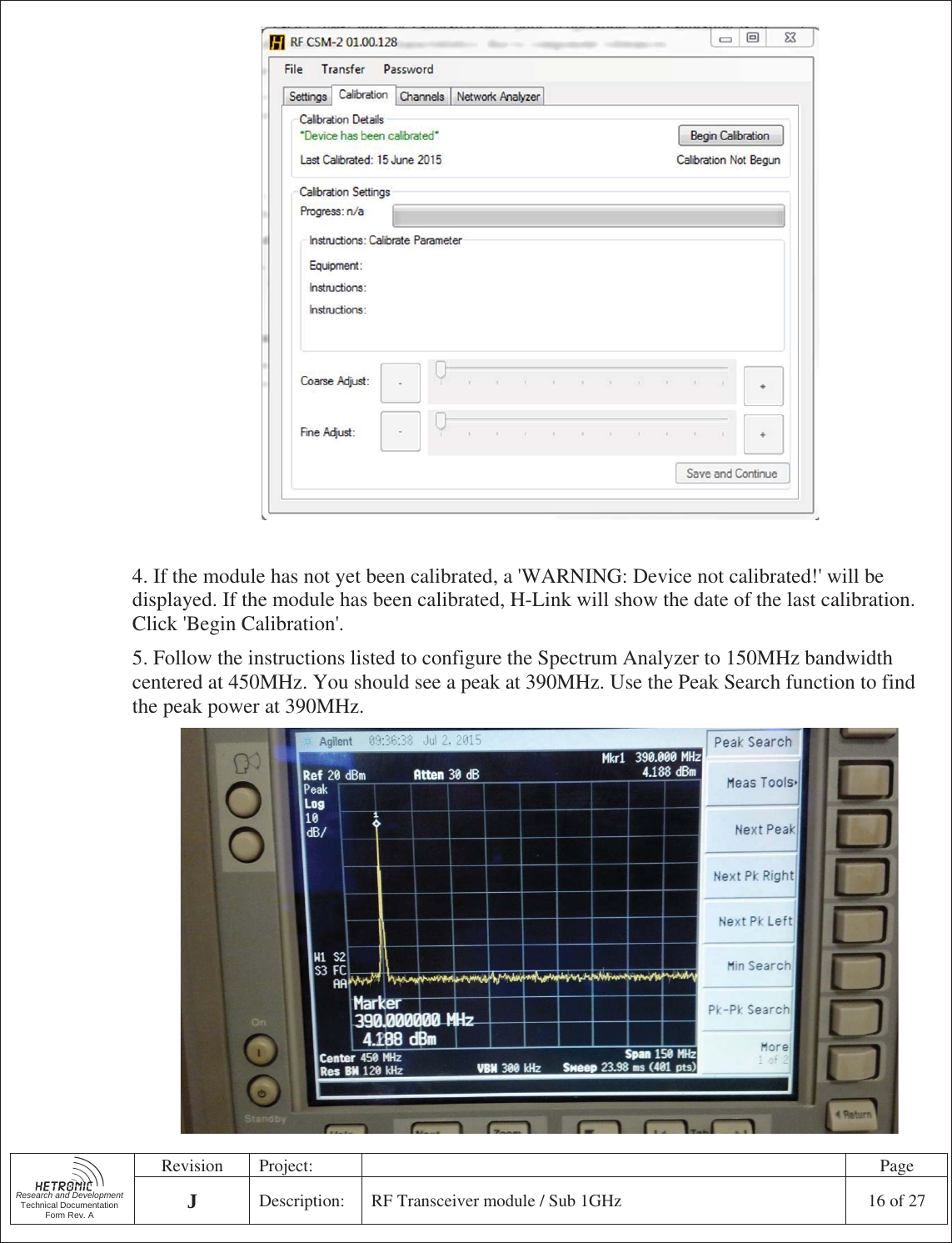
![Research and Development Technical Documentation Form Rev. A Revision Project: Page JDescription: RF Transceiver module / Sub 1GHz 20 of 27 2. The PC should display what the current un-calibrated power measurement is as "RSSI = [x]dBm". Use the "+" and "-" Coarse Adjust buttons to adjust the measured power level until it reads "-60dBm". 3. When finished, press 'Save and Continue'. Device Calibration is now complete. Before disconnecting the module, go to the 'Transfer' drop-down on the top bar and select 'Save Settings to Device'. Click 'Yes' when asked if user is sure, and wait for the settings to fully download. 4. When settings are finished downloading, close H-Link, open the J_US and J_VBUS jumpers before removing the module.](https://usermanual.wiki/Hetronic/CSM400UE/User-Guide-3429447-Page-20.png)