Hetronic CSM400UE Data Transceiver Module User Manual CSM 400UE Tech Docx
Hetronic International Inc Data Transceiver Module CSM 400UE Tech Docx
Hetronic >
User Manual
Revision Modified Checked Module Name
Date By Date By CSM-400UE
A Apr14-2015 BG
B Apr24-2015 BG
C June25-2015 BG Description
D July6-2015 BG
E July8-2015 BG RF Transceiver module / Sub 1GHz
F Aug11-2015 BG
G Aug26-2015 BG
H Oct14-2015 BG
I Oct16-2015 BG Remarks
J Mar16-2017 GWH
3.3~5.0Vdc / USB Flash programmable
Item Number
66990004
R&D
Technical
Documentation

Research and Development
Technical Documentation
Form Rev. A
Revision Project: Page
JDescription: RF Transceiver module / Sub 1GHz 2 of 27
1. TABLE OF CONTENTS
1.TABLE OF CONTENTS ................................................................................................................................ 2
2.PROJECT DESCRIPTION ............................................................................................................................. 3
3.BLOCK DIAGRAM ....................................................................................................................................... 4
4.TECHNICAL SPECIFICATION .................................................................................................................... 5
5.CONNECTION DIAGRAM ........................................................................................................................... 6
6.FUNCTIONAL DESCRIPTION ..................................................................................................................... 7
7.ASSEMBLY DESCRIPTION ......................................................................................................................... 8
8.MECHANICAL DRAWING ........................................................................................................................ 10
9.TEST PROCEDURE ..................................................................................................................................... 11
10.SCHEMATIC ............................................................................................................................................ 21
11.PCB ............................................................................................................................................................ 22
12.FIRMWARE .............................................................................................................................................. 24
13.ATTACHMENTS ...................................................................................................................................... 24
14.PARTS LIST .............................................................................................................................................. 25
15.REVISION HISTORY............................................................................................................................... 27
TABLE OF FIGURES
Figure 1: CSM-400UE Block Diagram .................................................................................................................. 4
Figure 2: CSM-400UE Connection Diagram ......................................................................................................... 6
Figure 3: CSM-400UE Top Lacquer Mask ............................................................................................................ 8
Figure 4: CSM-400UE Bottom Lacquer Mask ....................................................................................................... 8
Figure 5: RF Shield Solder Pads ............................................................................................................................. 9
Figure 6: CSM-400UE with Soldered Shield ......................................................................................................... 9
Figure 7: CSM-400UE Mechanical Drawing ....................................................................................................... 10
Figure 8: CSM-400UE Schematic ........................................................................................................................ 21
Figure 9: CSM-400UE PCB Layers ..................................................................................................................... 22
Figure 10: CSM-400UE Top Components ........................................................................................................... 23
Figure 11: CSM-400UE Bottom Components ...................................................................................................... 23

Research and Development
Technical Documentation
Form Rev. A
Revision Project: Page
JDescription: RF Transceiver module / Sub 1GHz 3 of 27
2. PROJECT DESCRIPTION
CSM-400UE is a modular 410-475MHz RF transceiver designed to provide the RF interface for Hetronic
devices. The module is designed to be mounted onto Hetronic coder and decoder boards to convert digital
information to RF signals and RF signals to digital information. CSM-400UE can be programmed to
function in several different operating modes. Configuring the operating mode and functional settings of
each mode allows CSM-400UE to be expandable to additional operating modes, new RF protocols and
many frequency channels. CSM-400UE communicates with a PC using the CSM-CFG board as an USB and
RS-232 adapter.
CSM-400UE uses an internal 3.1V regulator and requires a 3.3-5.0V external power supply. Absolute
maximum survival supply voltage is limited to 12VDC. In applications, this will be provided by the host
coder/decoder board. CSM-400UE can be configured to operate on any 6.25kHz channel from 410MHz -
475MHz. The RF output power is set to 10dBm (10mW). Depending on the protocol, CSM-400UE can
operate at RF baudrates up to 50kbps. CSM-400UE is built around the TI CC1200 Sub-1GHz RF
transceiver. RF front-end circuitry on the device limits effective performance to ~385MHz to ~500MHz,
although the hard frequency limits for the 400 MHz range are from 410 to 475 MHz. RF sensitivity varies
depending on the protocol being used.
All of the functionality of the CSM-400UE is configured in the firmware. CSM-CFG is also used to load the
firmware bootloader over RS-232 and firmware application using the USB Flash Programmer tool. CSM-
400UE can also connect to the PC H-Link tool over the CSM-CFG board. H-Link serves an important
purpose for CSM-400UE: calibrating the on-board radio. Every CSM-400UE module must be calibrated
before use in a Hetronic product. H-Link calibration compensates for production variation in the RF
performance of the on-board radio.
CSM-400UE by default is configured to 'ELP-TRx' mode. This causes it to act as a transceiver for the
Hetronic ELP protocol. In this mode it will only communicate with other ELP devices. In ELP Mode, radio
control and data transfer are all handled over the DI and DO pins with 115.2k baud UART. The legacy 'AF'
pin does not support audio output but is instead used for USB detection. CSM-400UE's frequency and
encryption can be configured using the CSM Configuration Tool. For more information, see the CSM_CFG
Technical Document.

Research and Development
Technical Documentation
Form Rev. A
Revision Project: Page
JDescription: RF Transceiver module / Sub 1GHz 4 of 27
3. BLOCK DIAGRAM
Figure 1: CSM-400UE Block Diagram
Research and Development
Technical Documentation
Form Rev. A
Revision Project: Page
JDescription: RF Transceiver module / Sub 1GHz 5 of 27
4. TECHNICAL SPECIFICATION
Parameter Specification
Nominal Supply (BATT+) 3.2~5.0Vdc
Max Supply (BATT+) 5.5V
Min Supply (BATT+) 2.9Vdc
Max Input Voltage on I/O pins 5Vdc
Operating Temperature Range -40°C ~ +80°C
Operating Frequency Range 410.0000MHz ~475.0000MHz
Channel Step 6.25 kHz minimum
Max Data Rate 50 kbps maximum
Antenna / Impedance SMB / 50ohms
TRANSMITTER - ELP
TX Operating Current 60mA
RF Output Power -10 to +10dBm (configurable)
Frequency Deviation 14 kHz (ELP, 4-GFSK, 50 kbps)
Spurious emission > -40dB
RECEIVER - ELP
RX Operating Current 60mA
Sensitivity -103 dBm (ELP, 4-GFSK, 50 kbps)
Adjacent Channel Selectivity 65dB
Research and Development
Technical Documentation
Form Rev. A
Revision Project: Page
JDescription: RF Transceiver module / Sub 1GHz 6 of 27
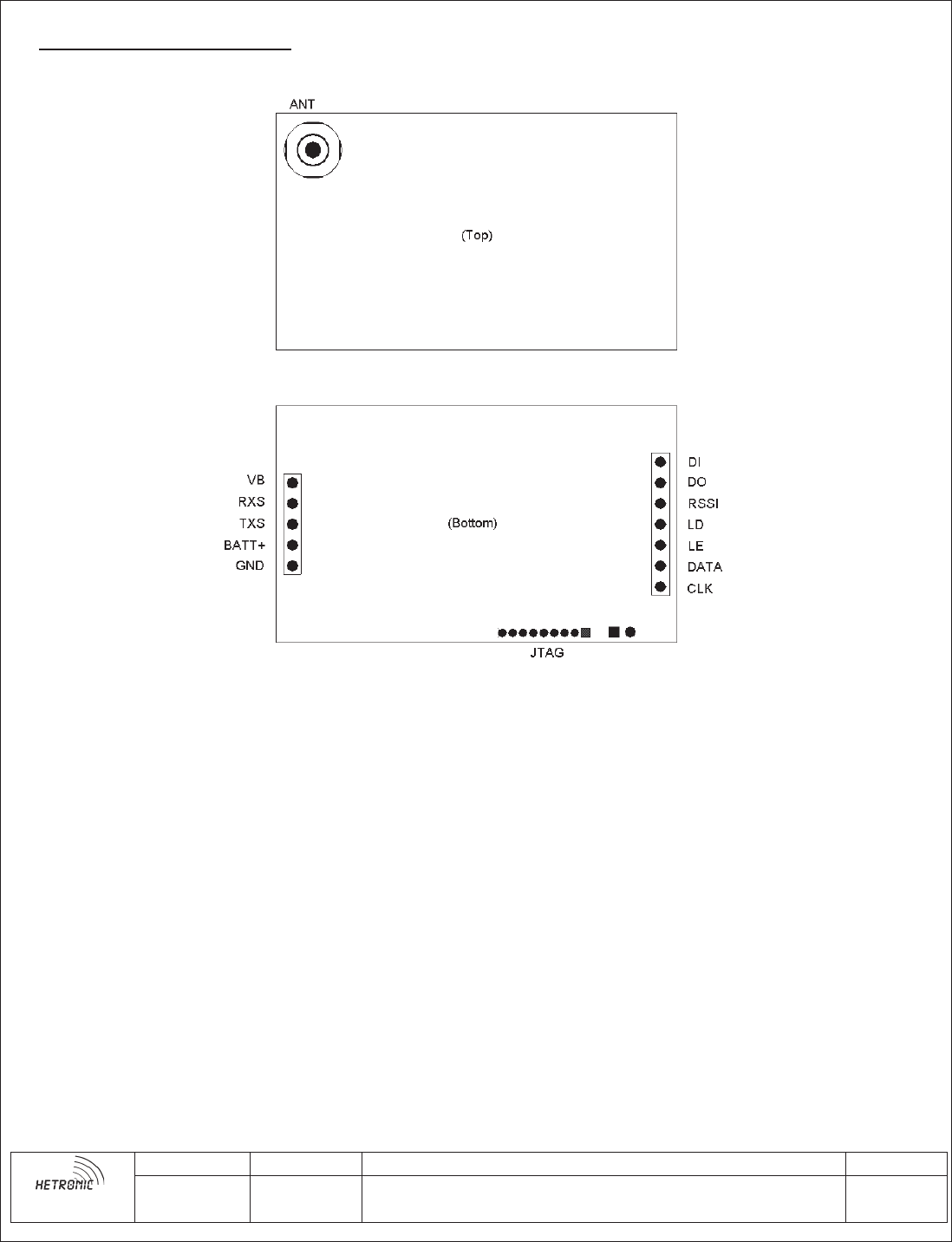
5. CONNECTION DIAGRAM
Figure 2: CSM-400UE Connection Diagram

Research and Development
Technical Documentation
Form Rev. A
Revision Project: Page
JDescription: RF Transceiver module / Sub 1GHz 7 of 27
6. FUNCTIONAL DESCRIPTION
6.1. Configuration
CSM-400UE is configured by the CSM Configuration Tool software. For more information on this
tool, see the CSM_CFG Tech Doc.
6.2. ELP Mode
In ELP Mode, the CSM-400UE acts as an ELP Transceiver. ELP is the Hetronic 'Event Link
Protocol', which operates at 50kbps baudrate, 4GFSK modulation and 6.25kHz deviation. In this
mode the radio can only be controlled and used with an ELP coder/decoder. Default output power is
set to 0dBm but can be configured to +/-10dBm. In ELP Mode, the device is centered on a 12.5kHz
channel, between 410MHz and 475MHz. In ELP Mode, CSM-400UE will only communicate with
other radios using ELP. ELP Mode also allows the CSM-400UE to enable/disable encryption of the
wireless data. Encryption-enabled and -disabled devices cannot communicate with each other.
6.3. Test Mode
In Test Mode, the CSM-400UE will function in one of several configurable Test Modes:
6.3.1. CW Test Mode
In CW Test Mode, the CSM-400UE will continually output a single-frequency tone for test
measurement purposes. The frequency and peak output power of the CW tone are configurable.
6.3.2. ELP Random Transmit Mode
In ELP Random Transmit mode, the CSM-400UE will continually transmit a random string of
data at the ELP settings: 50kbps, 4GFSK modulation with a 6.25kHz deviation.
6.3.3. ELP Random Receive Mode
In ELP Random Receive Mode, the CSM-400UE will continually receive any data broadcasted
with the ELP settings in the ELP packet structure.
Research and Development
Technical Documentation
Form Rev. A
Revision Project: Page
JDescription: RF Transceiver module / Sub 1GHz 8 of 27
7. ASSEMBLY DESCRIPTION
7.1. Lacquer Mask
Cover the marked areas of the board assembly before lacquering.
Use only Hetronic approved lacquer.
Figure 3: CSM-400UE Top Lacquer Mask
Figure 4: CSM-400UE Bottom Lacquer Mask
Research and Development
Technical Documentation
Form Rev. A
Revision Project: Page
JDescription: RF Transceiver module / Sub 1GHz 9 of 27
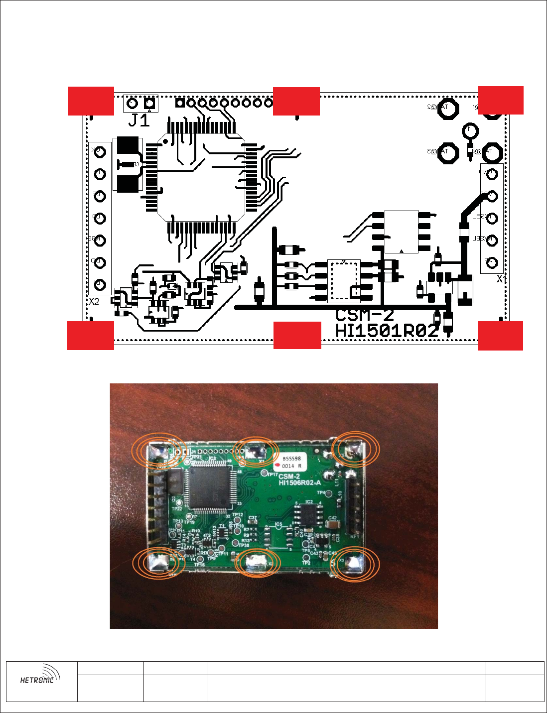
7.2. RF Shield
CSM-400UE should have the RF shield (Hetronic Part 18864 TEMP) soldered to the 6 ground pads
on the edge of the bottom side of the board. Ground pads are highlighted below. RF shield should not
be attached until after programming, testing and calibration.
Figure 5: RF Shield Solder Pads
Figure 6: CSM-400UE with Soldered Shield
Research and Development
Technical Documentation
Form Rev. A
Revision Project: Page
JDescription: RF Transceiver module / Sub 1GHz 10 of 27
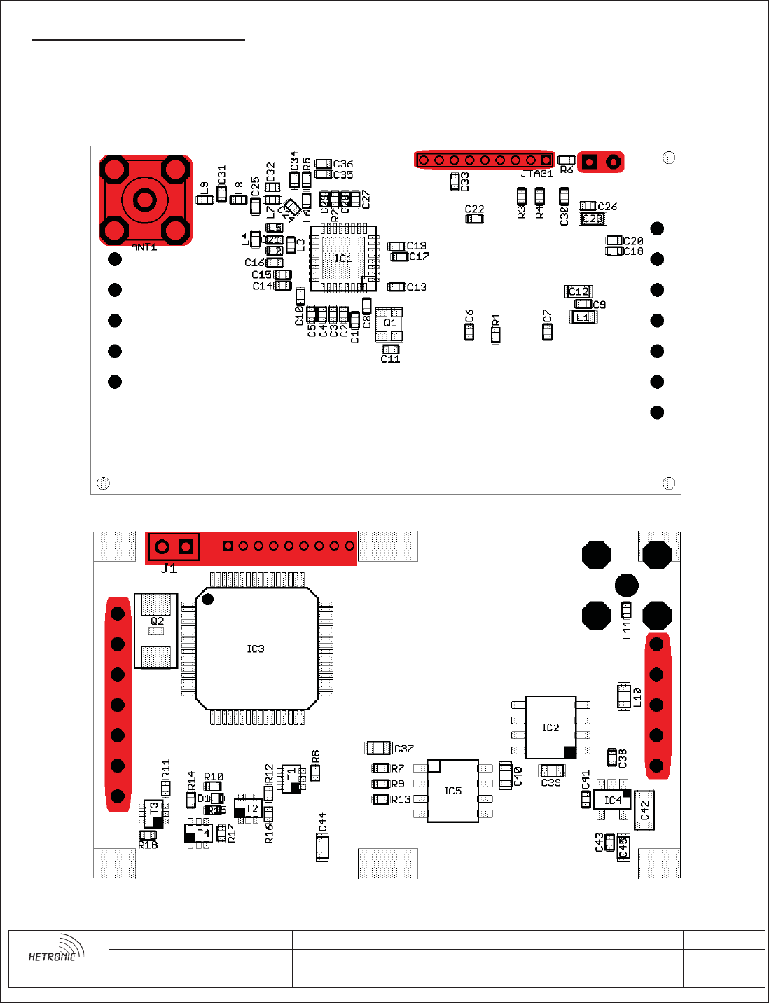
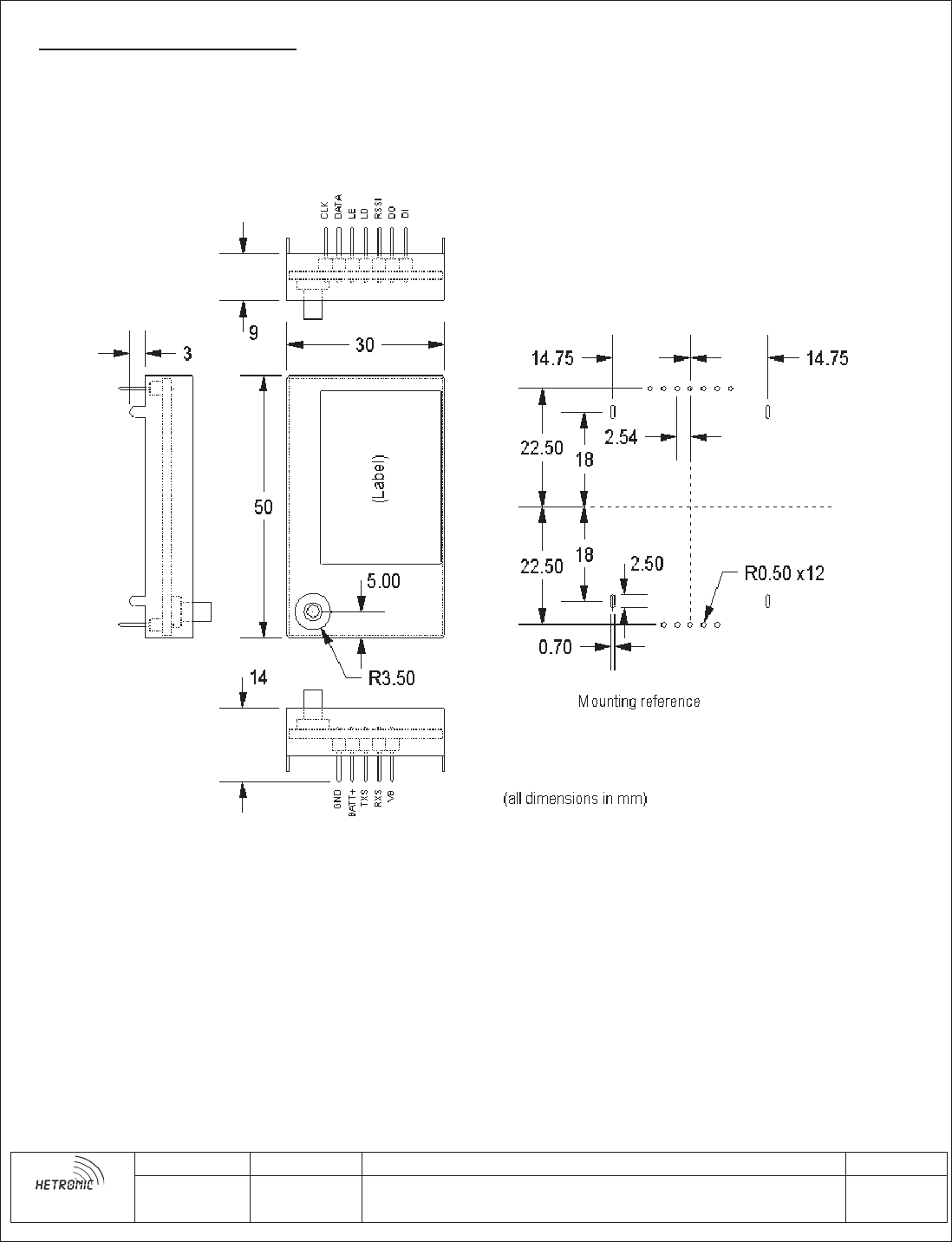
8. MECHANICAL DRAWING
Figure 7: CSM-400UE Mechanical Drawing
Research and Development
Technical Documentation
Form Rev. A
Revision Project: Page
JDescription: RF Transceiver module / Sub 1GHz 11 of 27
9. TEST PROCEDURE
9.1. Equipment Needed
1. CSM_CFG Adapter Board
2. USB Cable
3. RS-232 Cable
4. 5V DC Power Supply
5. SMB RF Cable
6. 1GHz Spectrum Analyzer
7. 1GHz RF Signal Generator
8. PC
9. H-Link PC Software and Dongle
10. Digital Multimeter
11. STMicroelectronics Flash Loader software
12. Hetronic USB Flash Programmer software
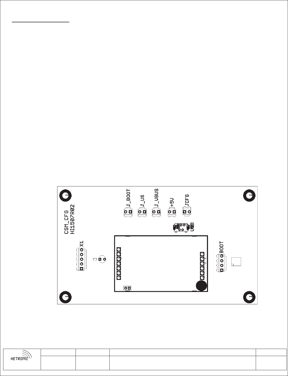
9.2. Power Supply Verification
1. Install the device in the CSM_CFG adapter. See figure below for connector reference:
2. Connect the adapter to the PC using a USB cable.
3. Short the J_US jumper.
4. Using DMM, verify 3.1V on the left-most pin of JTAG connector (closest to J1)
Research and Development
Technical Documentation
Form Rev. A
Revision Project: Page
JDescription: RF Transceiver module / Sub 1GHz 12 of 27
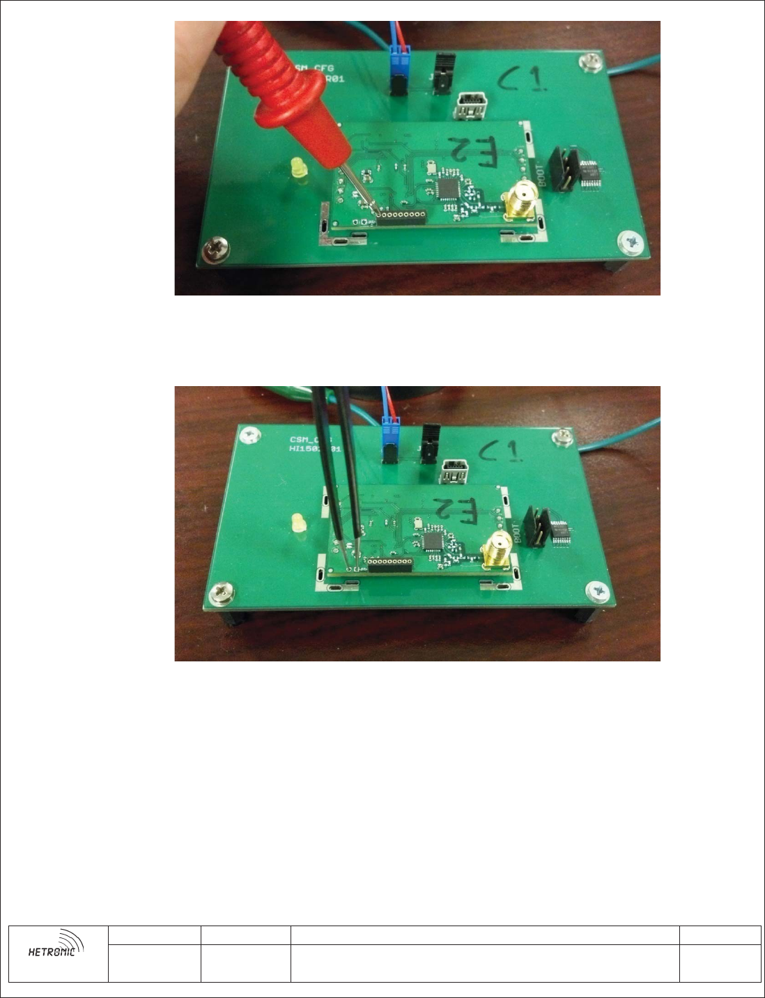
9.3. Bootloader Programming
1. Open the J_US jumper to remove power
2. Short connector J1 on device to start device in boot mode
3. Short the J_US jumper to apply power
4. Connect RS-232 cable to connector BOOT on CSM_CFG
5. Start STMicro Flash Loader
6. Set appropriate COM port and other UART settings, then click Next
Research and Development
Technical Documentation
Form Rev. A
Revision Project: Page
J
Description: RF Transceiver module / Sub 1GHz 13 of 27
7. On the following 'Target is Readable' page, click Next. On the following 'Target Select' page, click
Next.
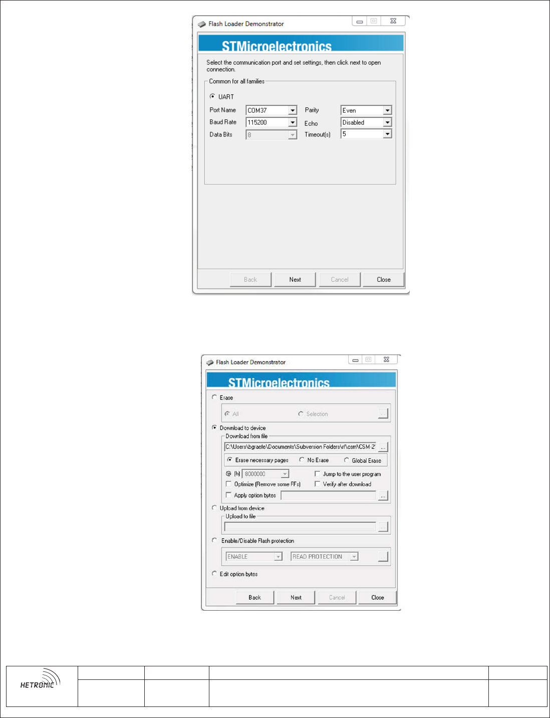
8. On the following page, select 'Download to device' and browse to bootloader.hex. Then click Next.
9. Wait for the Flash Loader to finish loading and the 'Download operation finished successfully' is
displayed. Then click Close.
Research and Development
Technical Documentation
Form Rev. A
Revision Project: Page
JDescription: RF Transceiver module / Sub 1GHz 14 of 27
10. Disconnect RS-232 cable from CSM_CFG. Remove 5VDC from CSM_CFG. Open jumper J1 on
CSM400UE.
9.4. Main Flash Application Programming
1. Open jumper J_US to remove power
2. Close jumper J_VBUS, then close jumper J_US to put the module in boot mode
3. Verify solid yellow LED on CSM_CFG
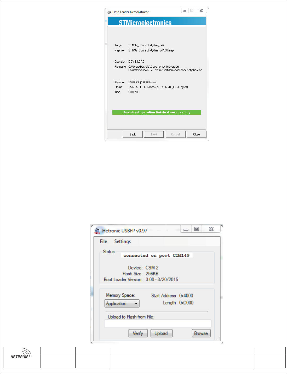
4. Start the USB Flash Programmer program.
5. After the USBFP connects to the CSM400UE, set the Memory Space to Application
Research and Development
Technical Documentation
Form Rev. A
Revision Project: Page
JDescription: RF Transceiver module / Sub 1GHz 15 of 27
6. Click Browse to select csm2_app_rx.hex.
7. Click Upload. On the pop-up window click Yes.
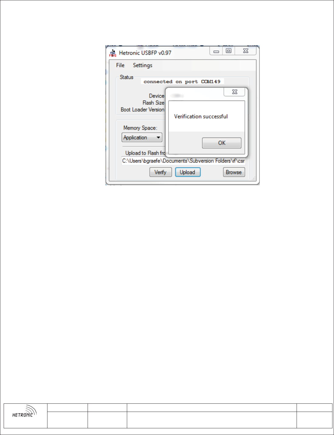
8. Wait for the loading to complete. On the Verification successful window click OK.
9. Close the USBFP software. Remove the USB cable from the CSM_CFG.
9.5. Calibration
After programming, each CSM-400UE must be calibrated at least once prior to operation. This
calibration is to compensate for small variations in RF characteristics due to component tolerances.
9.5.1. Output Power Calibration
The output power of the module varies across its frequency range; this calibration procedure
applies an internal offset to the output power depending on frequency to compensate for that
variation:
1. Insert CSM-400UE into CSM_CFG and connect the USB cable. Connect CSM-400UE ANT
to a calibrated Spectrum Analyzer using low-loss cable.
2. Close the J_US jumper, then J_VBUS. Insert the H-Link dongle into the PC.
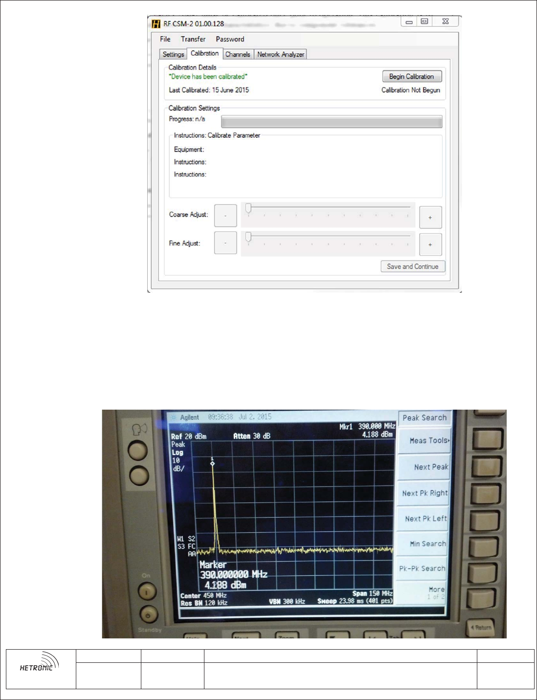
3. Start the H-Link software. Press "Connect". This should load the CSM-400UE H-Link
configuration menu. Go to the 'Calibration' tab.
Research and Development
Technical Documentation
Form Rev. A
Revision Project: Page
J
Description: RF Transceiver module / Sub 1GHz 16 of 27
4. If the module has not yet been calibrated, a 'WARNING: Device not calibrated!' will be
displayed. If the module has been calibrated, H-Link will show the date of the last calibration.
Click 'Begin Calibration'.
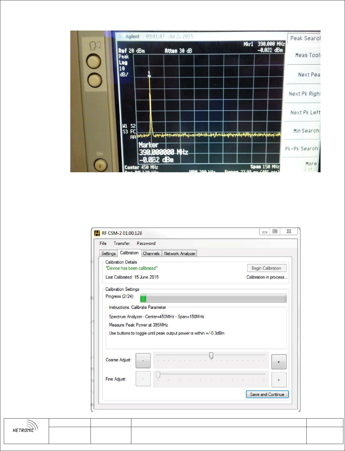
5. Follow the instructions listed to configure the Spectrum Analyzer to 150MHz bandwidth
centered at 450MHz. You should see a peak at 390MHz. Use the Peak Search function to find
the peak power at 390MHz.
Research and Development
Technical Documentation
Form Rev. A
Revision Project: Page
J
Description: RF Transceiver module / Sub 1GHz 17 of 27
6. Use the "+" and "-" Coarse Adjust buttons to increase or decrease the peak power at 390MHz.
Continue adjusting the power until it is with +/- 0.3dB of 0dBm.
7. When the peak is within +/-0.3dBm, click 'Save and Continue', then click 'Yes' when
prompted 'are you sure?'. This will move the peak frequency to 395MHz.
8. Repeat Step 6 and 7 for 395MHz, and each incremental frequency after that. The frequency
will continue to increment by 5MHz up to 475MHz. After the 475MHz peak is calibrated, click
'Save and Continue' to continue to Frequency Calibration.

Research and Development
Technical Documentation
Form Rev. A
Revision Project: Page
J
Description: RF Transceiver module / Sub 1GHz 18 of 27
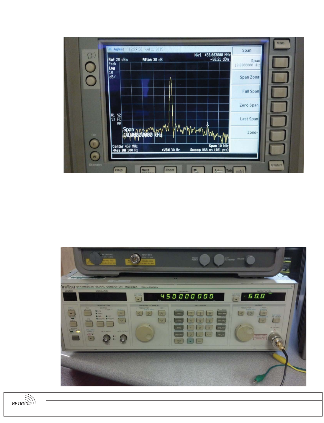
9.5.2. Frequency Calibration
This procedure fine-tunes the frequency setting of the module by applying a constant offset to
the Frequency Synthesizer.
1. Follow the instructions displayed to configure the Spectrum Analyzer: set Center Frequency to
450MHz, Span to 100kHz, Resolution BW to 100Hz and Video BW to 30Hz. This should show
the frequency synthesizer error more precisely.
2. Use the "+" and "-" Coarse Adjust buttons to increase/decrease the frequency from the module
until it is approximately centered at 450MHz.
Research and Development
Technical Documentation
Form Rev. A
Revision Project: Page
JDescription: RF Transceiver module / Sub 1GHz 19 of 27
3. Configure the Spectrum Analyzer span to 10kHz to see the frequency error more precisely.
Use the "+" and "-" Fine Adjust buttons to increase/decrease the frequency from the module until
it is exactly 450MHz.
4. When finished, press 'Save and Continue'.
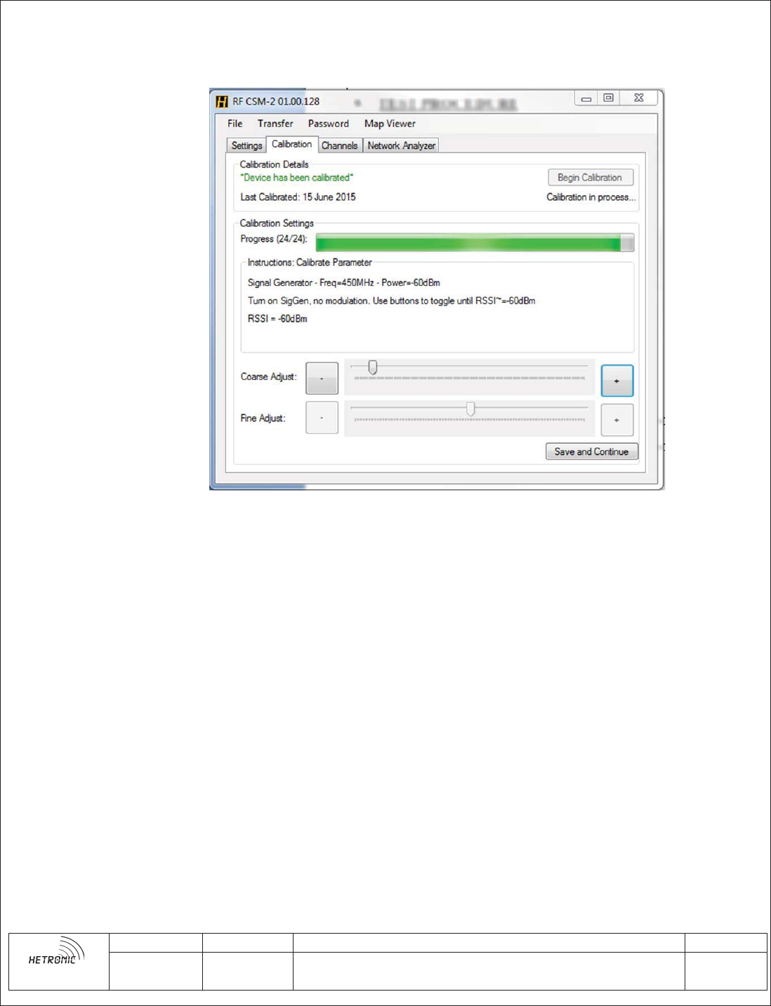
9.5.3. RSSI Calibration
The CSM-400UE has a built-in power detector capability. This calibration sets the reference
level so the power detector can return received RF power in dBm:
1. Connect the output of the RF Signal Generator to the antenna port of the radio module using a
low-loss cable. Configure the Signal Generator to output 450.000000MHz, no modulation, at a
power of exactly -60dBm.
Research and Development
Technical Documentation
Form Rev. A
Revision Project: Page
J
Description: RF Transceiver module / Sub 1GHz 20 of 27
2. The PC should display what the current un-calibrated power measurement is as "RSSI =
[x]dBm". Use the "+" and "-" Coarse Adjust buttons to adjust the measured power level until it
reads "-60dBm".
3. When finished, press 'Save and Continue'. Device Calibration is now complete. Before
disconnecting the module, go to the 'Transfer' drop-down on the top bar and select 'Save Settings
to Device'. Click 'Yes' when asked if user is sure, and wait for the settings to fully download.
4. When settings are finished downloading, close H-Link, open the J_US and J_VBUS jumpers
before removing the module.