Hitachi Kokusai Electric America AT725P 25 Watt UHF ATSC Transmitter User Manual AT725P Owner s Manual
Hitachi Kokusai Electric America LTD 25 Watt UHF ATSC Transmitter AT725P Owner s Manual
Exhibit D Users Manual per 2 1033 c3
Linear Industries, Inc.
AT725P
Owner’s Manual
August 2009

AT725P Owner’s Manual
© 2009 Linear Industries, Inc. All Rights Reserved AT725P_OM_08/09 2/75
Linear AT725P
25W UHF 8VSB-ATSC EXCITER/TRANSMITTER
Owner Manual
Table of Contents
Section 1:
General Description,
Technical Specifications,
Typical Final Test Report
Section 2:
Control Unit
Section 3:
DTV Modulator
Section 4:
Up Converter
Section 5:
Power Amplifier
Section 6:
Power Supply
Section 7:
DC-DC Converter
Section 8:
Memory Interface
Annex A:
Operational Software
Annex B:
Checking the LDMOS transistors
Annex C:
Typical Final Test Report Results

AT725P Owner’s Manual
© 2009 Linear Industries, Inc. All Rights Reserved AT725P_OM_08/09 3/75
User Notices and WARNINGS
USER NOTICES
IT IS VERY IMPORTANT TO READ THIS MANUAL PRIOR TO OPERATION OF
THIS TRANSMITTER!
Notice 1
The transmitter main operating voltage setting is marked on the rear of the AT7350-
1 chassis.
Notice 2
The transmitter operating frequency is set from the factory.
Notice 3
For adjusting the RF output power setting a qualified technician should always
employ the use of an RF Wattmeter and a calibrated dummy load.
Notice 4
Should accident or injury occur to the personnel engaged in the installation,
operation, or service of the equipment, they should seek proper medical attention. It
is advisable that such personnel have familiarity with first-aid practices.
Notice 5
For technical support please call the Linear technical support customer service line
at 847/428-5793 ext. 105.
Notice 6
The technical information presented on this manual is sole intellectual propriety of
Linear Industries, Inc. Reproduction of this document in full or partial is prohibited
without written authorization. This document is legally protected by the copyright
laws.

AT725P Owner’s Manual
© 2009 Linear Industries, Inc. All Rights Reserved AT725P_OM_08/09 4/75
WARNING!
THE VOLTAGES AND CURRENTS IN THIS EQUIPMENT ARE DANGEROUS.
PERSONNEL MUST, AT ALL TIMES, OBSERVE SAFETY WARNINGS,
INSTRUCTIONS, AND ANY LOCAL REGULATIONS.
THIS OWNER’S MANUAL IS INTENDED AS A GENERAL GUIDE FOR TRAINED
AND QUALIFIED PERSONNEL WHO ARE AWARE OF THE DANGERS THAT
ARE INHERENT IN THE HANDLING AND OPERATION OF POTENTIALLY
HAZARDOUS ELECTRICAL AND ELECTRONIC CIRCUITS. IT IS NOT THE
INTENT OF THIS MANUAL TO PROVIDE A COMPLETE SET OF SAFETY
INSTRUCTIONS OR PRECAUTIONS THAT SHOULD ALREADY BE
UNDERSTOOD BY TRAINED OR EXPERIENCED PERSONNEL IN USING THIS
OR OTHER TYPES AND FORMS OF ELECTRONIC EQUIPMENT.
THE INSTALLATION, OPERATION, AND MAINTENANCE OF THIS EQUIPMENT
INVOLVE RISKS TO PERSONNEL AND ALSO TO THE EQUIPMENT. LINEAR,
INC. SHALL NOT BE RESPONSIBLE FOR INJURY OR DAMAGE THAT IS THE
RESULT OF IMPROPER PROCEDURES OR USE BY INDIVIDUALS
IMPROPERLY TRAINED OR LACKING THE KNOWLEDGE TO PERFORM
ASSOCIATED TASKS.
ALL LOCAL CODES FOR BUILDING, SAFETY, FIRE, OR RELATED STANDARDS
MUST BE OBSERVED. CONSULT LOCAL AUTHORITIES FOR THE
STANDARDS FOR THE AREA OR REGION WHERE THE EQUIPMENT WILL BE
INSTALLED AND PUT IN USE.
WARNING!
AT ALL TIMES DISCONNECT AC/MAIN POWER BEFORE OPENING COVERS,
DOORS, ENCLOSURES, PANELS, OR PROTECTIVE SHIELDS THAT EXPOSE
LIVE CIRCUITS. NEVER PERFORM MAINTENANCE, MAKE ADJUSTMENTS, OR
SERVICE THE EQUIPMENT WHEN ALONE OR FATIGUED.
WARNING!
IF ELECTROLYTIC OR OIL FILLED CAPACITORS ARE UTILIZED IN THE
EQUIPMENT AND THE COMPONENT APPEARS LEAKY, OR IS BULGING, OR IF
THE CASE OR COVERING OF THE COMPONENT APPEARS DAMAGED OR
DISTRESSED, ALLOW SUFFICIENT TIME FOR THE UNIT TO COOL OR FULLY
DISCHARGE BEFORE SERVICING. SERVICING HOT OR LEAKY CAPACITORS
CAN CAUSE A RUPTURE OF THE CASE AND POSSIBLE INJURY.

AT725P Owner’s Manual
© 2009 Linear Industries, Inc. All Rights Reserved AT725P_OM_08/09 5/75
Returns and Exchanges
Equipment (Damaged or undamaged) should not be returned unless written
approval and a Merchandise Return Authorization (MRA Number) is received from
your Linear Sales representative or Linear Customer Service. Special shipping
instruction will be provided which will assure proper handling. The circumstances
and reasons for the return must be included in the request for return. Equipment
that is special or “custom” ordered may be not returnable. In situations where return
or exchange is at the request of the customer a restocking fee may be charged. All
returns must be sent freight prepaid and properly insured by customer. When
communicating with Linear please refer to your Order or Invoice Number.
Unpacking
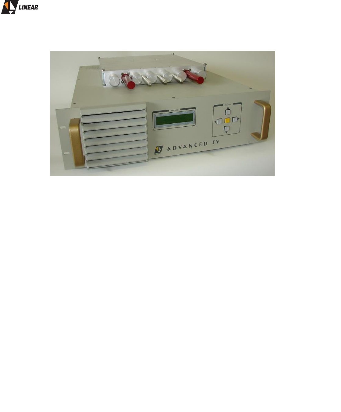
Use care when unpacking the equipment. First perform a visual inspection of the
item(s) to determine if any damage occurred during shipment. Be sure to retain all
the shipping materials (crates and boxes or cartons) until such time that it has been
determined that the received equipment arrived undamaged. Find all PACKING
LISTS and keep them to assist in locating and identifying any components or
assemblies that may have been removed for shipping and might need to be
reinstalled in the equipment. Make sure that all shipping straps, supports and
packing materials are completely removed from the equipment prior to initialization
and use.
AT725P Owner’s Manual
© 2009 Linear Industries, Inc. All Rights Reserved AT725P_OM_08/09 6/75
Section 1 – AT725P General Description
1. General Description
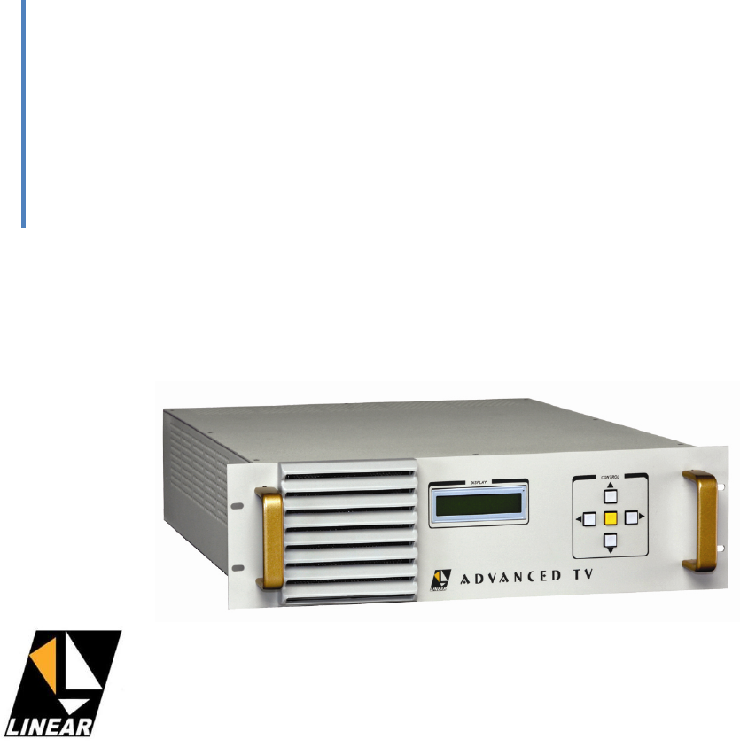
The ATSC DTV exciter model AT725P is part of the ADVANCED TV line, with modular construction to fit in a
19” EIA standard rack and including the following modules:
• 01 Main Control unit - CIM3297
• 01 Keypad - CIM3003
• 01 Display LCD 20 columns x 02 lines - CIM3004
• 01 Memory interface - CIM3535
• 01 1Mbits memory card - CIM3516
• 01 25W RMS UHF/ATSC - Module 4408
• 01 up-Digital Converter - Module 4492
• 01 Power Supply - Module 4401 (versions M110/M220/B220)
• 01 8VSB Modulator and Master Clock Generator - Module 4549
• 01 DC/DC Converter (+2.5V and +5V)
When an AT725P is installed as a TRANSMITTER, a 6 poles elliptical filter is installed at its RF Output. The
additional insertion loss is considered and the unit is pre-corrected and equalized accordingly. In this
application, the overall performance of the unit will meet or exceed the FCC requirements for out of the
channel spurious emission. Please refer to Annex C.
One will also need to perform an operational software operation, to set the unit as TRANSMITTER. Please
refer to Annex A, SET CONFIGURATION at page 64.
AT725P Owner’s Manual
© 2009 Linear Industries, Inc. All Rights Reserved AT725P_OM_08/09 7/75
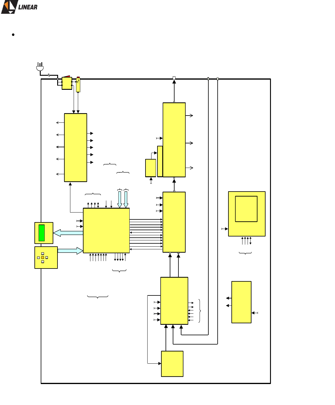
AT725P Block Diagram:
C O N T R O L U N IT
C IM 3 2 9 7
(C I P 8 2 3 1 )
+8V
+15V
R E S T A R T
R F O U T
2 0W A M P .T E M P E R A T U R E
M A S TE R C L O C K L O C K D E T E C T
E X C I T E R F O R W A R D P O W E R
E X C I T E R R E F LE C T E D P O W E R
2 0W E X C I T E R ID C U R R E N T
+ 32 V P O W E R S U P P L Y
+ 18 V P O W E R S U P P L Y
-1 8V P O W E R S U P P L Y
+ 9V P O W E R S U P P L Y
+32V
O U T P U T
CURRENT
R E A D IN G
+9V-18V
+18V
+32V
F IX O
+32V
R E A D IN G
+18V
R E A D IN G
-18V
R E A D IN G
+9V
R E A D IN G
+32V
R E S .
P O W E R S U P P L Y
M O D U L E 4 40 1
110V / 220V
M O N O P H A S IC
A N D B IP H A S IC
O N /O F F
S W I C T H
5 A / 2 2 0 V
1 0 A / 1 1 0 V
F U S E
R E A D IN G S
A L A R M S
+32V
R E S T A R T E D
2 0 W U H F A T S C A M P L IF IE R
M O D U L E 4 40 8
T E M P E R A T U R E
A L A R M
F O R W A R D P O W E R
R E A D IN G
F A N
F A N
F IL T E R
C I M 6 6 7 3
+24V
+32V
F IX O
IN O U T
8 V S B
M O D U L A T O R A N D
M A S T E R C L O C K
U H F U P C O N V E R T E R
M O D U L E 4 49 2
+18V-18V
QIN
RF
O U T
S W 2
T E M P
E N A B L E Q D A C
E N A B L E I D A C
C L O C K D A C
D A TA D A C
A L C
+32V
F IX O
IIN
S W 1
E N A B L E
D A TA P L L
C L O C K P L L
L O C K D E TE C T
K E Y B O A R D
C I M 3 0 0 3
LI N E AR E QU I P A M E N TO S E L E T R Ô N IC O S
D IS P L A Y
C I M 3 0 0 4
S M P T E IN
A S I IN
1 0 M H z R E F IN
M O D U L E 4 54 9
+32V
M O D U L E 4 5 6 7
D C C O N V E R T E R
+5V+ 2 .5 V
+5V+ 2 .5 V +18V-18V
R E F L E C TE D P O W E R
R E A D IN G
1 0 M H z
O C X O
M O D U L E 4 2 8 1
R S 2 3 2
E X T E R N A L
F U N C TIO N S
P A IN E L
T R A S E IR O
RD
E N A
C L K
D IN
DO
LD
M E M O R Y
M E M O R Y
C A R D
C A R D
C IP 8 4 2 1
C IP 8 4 2 1
M E M O R Y IN T E R F A C E
M E M O R Y IN T E R F A C E
C IP 8 4 3 7
C IP 8 4 3 7
+5V
D C L K
A S D I
C S
D A T A
F R O M
C O N T R O L
U N IT
RD
E N A
C L O C K
D IN
DO
M O D U L A TO R
C O N T R O L U N IT
D C L K
A S D I
CS
D A T A
T O
M E M O R Y
IN T E R F A C E
Fig. 1.1: AT725P - Block Diagram

AT725P Owner’s Manual
© 2009 Linear Industries, Inc. All Rights Reserved AT725P_OM_08/09 8/75
Module 4549
8VSB Modulator section
The 8VSB modulator automatically recognizes the incoming transport stream, either
SMPTE310M or ASI. The transport stream input is a BNC connector located on the rear
panel of the unit. The modulated output signal of this module is composed by two IF
orthogonal carriers termed; signals (I) and (Q). The central frequency of the 8VSB
modulated IF signal is 18.83339MHz. The signal processing and modulation performed on
this module follows the ATSC recommendation A/53 E.
In this modulator, the in-factory non-linear pre-correction that may be necessary to enhance
the equipment’s efficiency and meet the FCC’s spurious emissions’ requirements are
performed. If an RF output filter is required (AT275P being set up as a transmitter), the
recommended linear equalization is also factory performed in this section.
Master Clock section
The master clock unit generates via PLL and VCO’s type oscillator at 172.16MHz. The PLL
loop is locked to a 10MHz reference, externally or internally generated. This signal is the
time base for the 8VSB modulator
Module 4492
IF to UHF up-Converter section
The IF orthogonal carriers (I) and (Q) are generated on module 4549, (8VSB Modulator
section), and are routed to the up-converter module. The output signal of this module is set
on the FCC/UHF operational 6MHz channel of the exciter AT725P.
Internally, the modulated IF band mixes with the continuous wave local oscillator LO. As
result of this mixing, the IF translation to the UHF band is performed. The LO is a free
oscillator, that has its frequency locked via PLL. The LO/PLL use a 10MHz OCXO (oven
controlled crystal oscillator) type, or an external reference.
10MHz reference automatic switching section
Both circuits, the 8VSB modulator and the up-converter share the same source of reference
signal they need. The use of the same reference allows a perfect synchronization and
stability during the DTV transmission process. The internal 10MHz signal is gotten from an
OCXO oscillator @ 0.3ppm. The external 10MHz signal can use as reference a GPS signal
for instance.

AT725P Owner’s Manual
© 2009 Linear Industries, Inc. All Rights Reserved AT725P_OM_08/09 9/75
The external reference input is a BNC connector located on the rear panel of the unit. In the
absence of this external source, automatically the commutation for the internal source of
10MHz will be made generated by OCXO.
Module 4408
25W UHF band multistage amplifier section
The IF modulated signal already converted into UHF is amplified by an UHF amplifier of
25W. This module uses transistors built with LDMOS technology operating in class AB, with
excellent ratio between efficiency and linearity. The RF OUT connector of the unit is the
output of this module.
RF Output sample section
The module 4408’s RF sample, detects the direct and reverse RF power present on the RF
OUT connector of the unit. These two detected samples are then converted on
correspondent DC levels before being routed to the master control unit, where they will be
processed and displayed on the front panel, LCD screen in unit watts.
CIM3297
Control unit card
The digital management of the transmitter of DTV AT725P is made by the control unit card
CIM3297. This control unit utilizes an A128 microcontroller programmed in the assembler
language, which makes the process data related with the following parameters:
• Alarm of loss of the lock of the PLL of up-converter.
• Alarm of excess temperature of the 25W amplifier.
• Monitor and exhibit the RF direct and reflected powers, out from the 25W amplifier, muting
the transmission in case of extreme levels.
• Exhibits of level electrical current, I1 from the main power supply.
• Process and exhibit the voltages generated by the power supplies.
• Set the Up-converter unit with the operational channel and transmitted power level via ALC.
The control unit is directly connected to a keypad and LCD screen both located on the front
panel of the exciter AT725P, from where monitoring and parameters can be set. The same
functions can be performed via the RS232 communication connection to a HyperTerminal.
Module 4401
AT725P Owner’s Manual
© 2009 Linear Industries, Inc. All Rights Reserved AT725P_OM_08/09 10/75
Power Supply
The power supply module is a switching power supply type, running on half-bridge topology.
It measures and informs the control unit, the current nominal value of the +32volts DC power
supply, and also measures the electrical current demanded by the entire exciter. Both the
voltage and the current data are routed to the control unit card to be processed and
displayed.
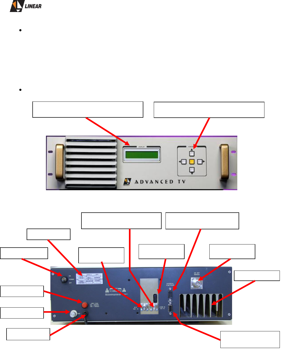
AT725P External Interfaces
Fig.1.2: AT725P Front View
Fig.1.3: AT725P Rear Panel View
20 X 2 - LCD Screen – Visual Interface for
SETUP and MEASUREMENTS
Power Switch
Command KEYPAD – Interface for readings and
data entry.
ID Tag
External 10MHz
Reference Input
GND
Main Fuse
ASI/SMPTE310M Transport
Stream Input
Internal DB-9
Not Used
ON/OFF the air External
Functions (DB-9)
AC Power Cord
RF Output
Connector
(DB-9) RS232
Hyper-terminal Interface
Hot Air Outlet
AT725P Owner’s Manual
© 2009 Linear Industries, Inc. All Rights Reserved AT725P_OM_08/09 11/75
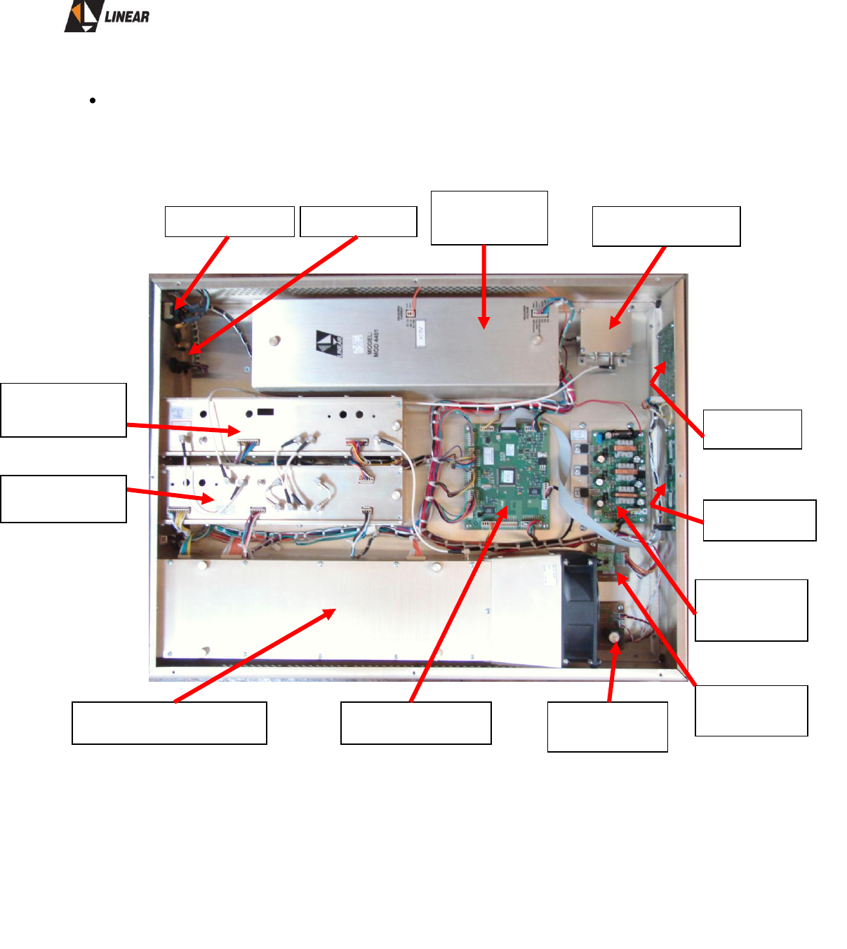
AT725P - Modules and Parts Displacement
Fig.1.4: AT725P Modules and Parts displacement
Key Pad
CIM3003
RF Power Amplifier
Module 4408
LCD Screen
CIM3004
LUT
Module 3535
DC/DC
Converter
Module 4567
DC Fan Filter
CIM6673
Digital Control Card
CIM3297/CIP8231A
+32V Power
Supply Module
4401
Ref. 10MHz OCXO
Module 4281
Power Switch
Fuse & GND
Up Converter &
Master Clock
Module 4492
8VSB Modulator
Module 4549

AT725P Owner’s Manual
© 2009 Linear Industries, Inc. All Rights Reserved AT725P_OM_08/09 12/75
AT725P - 25W UHF ATSC/8VSB Exciter- Transmitter - Technical Specifications
Electrical
Main
110/220 VAC, bi phase, 50-60 Hz.
Consumption
400W.
Power Factor Correction, FPC.
Included
Signal Input
Transport Stream Input
ATSC/MPEG2, compliant to SMPTE310M
Input Data Rate
19.39 Mbps
External Reference Signal
10MHz. (0 to +10 dBm).
Input Connector
75Ω (BNC),
Reference Input Connector
50Ω (BNC),
RF
Modulation Mode
8VSB.
IF
18.833916 MHz.
Channel Bandwidth
6MHz.
Test Signal
PRBS
Frequency Range
UHF. C14 to Ch59, (3 bands).
Frequency Step
1 Hz. ± 220kHz
Symbol Rate
10.76 MSymbol/sec.
Digital/Analog Converter
16 bit
Linearization Pre-Correction
Included
Pilot frequency stability overall
± 4.6 ppm.
Initial tolerance
± 1.0 ppm.
Vs. temperature in operating temperature range (steady state)
± 10 ppb.
Holdover 24 hours, full temp. range
± 12 ppb.
24 hours drift (after 30 days)
± 1.0 ppb.
Long term stability over 15 years
± 3.5 ppm.
Peak to peak frequency response
0.15 dB.
Peak to peak group delay response
10 ns.
Phase noise
≤ -104 dBc/Hz @ 20kHz offset.
Conducted spurious and harmonics
< -60 dBc, FCC 47 Part 74.
Radiated spourious and harmonics
< -80 dBc, FCC 47 Part 74.
MER (Modulation Error Rate)
≥ 29 dB (transmitter output) typical.
RF output connector
N
Communication
Hyper-terminal
RS232 (DB-9)
External Command – ON/OFF
(DB-9)
Mechanical
Air speed over drawers
25 ft/minute.
Dimensions
3UR (H), 19”(W), 26”(D)
Weight
Gross: 11 Kg
AT725P Owner’s Manual
© 2009 Linear Industries, Inc. All Rights Reserved AT725P_OM_08/09 13/75
Section 2 – Control Unit
General Functional Description
The DIGITAL CONTROL UNIT is responsible for all the digital management of AT725P exciter-
transmitter. Management and operability of the transmission is performed via key pad access
located on the front panel or via the RS232 through the hyper-terminal.
Its main attributes include:
• Management of the alarm of loss of the Lock of the PLL of Up-Converter.
• Management of the alarm of excess of temperature of the 25W amplifier.
• Monitor and exhibit the direct and reverse RF power at 25W level. In case of extreme
levels, the transmission will shut down.
• Display the main electrical current value, I1, drained from the main power supply.
• To process and show the power supply voltages.
• Perform the IF/RF Up-conversion control and transmitted power level control, (ALC).
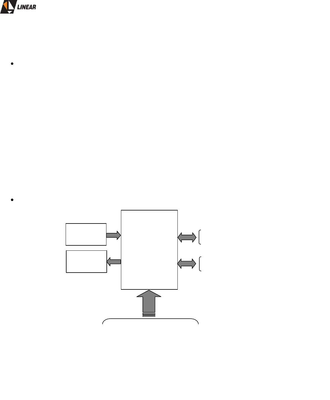
Control unit block diagram
Fig.2.1: Control unit general block diagram
CONTROL
UNIT
CIP8231
(CIM3297)
MICROCONTROLLER
DISPLAY
CIM3004
KEYBOARD
CIP8002
(CIM3003)
EXCITER FORWARD POWER READING
EXCITER REFLECTED POWER READING
EXC.20W ID CURRENT READING
VOLTAGES SUPPLY READINGS
RS232 REMOTE CONTROL
EXTERNAL FUNCTIONS
AT725P Owner’s Manual
© 2009 Linear Industries, Inc. All Rights Reserved AT725P_OM_08/09 14/75
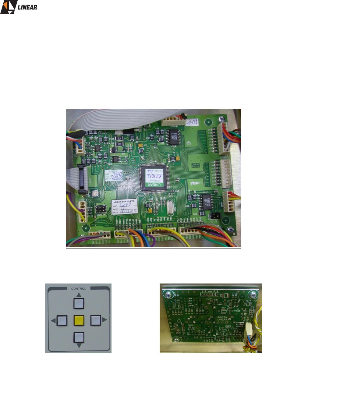
The PCB board CIP8231 is called generically the CONTROL UNIT, as it is the main component
of the DIGITAL CONTROL UNIT within the AT725P.
Fig.2.1, profiles the main components and connections of the Control Unit.
Fig.2.1 control unit board - CIP8231 (CIM3297)
Fig.2.2. Keypad board - CIP8002 (CIM3003)
AT725P Owner’s Manual
© 2009 Linear Industries, Inc. All Rights Reserved AT725P_OM_08/09 15/75
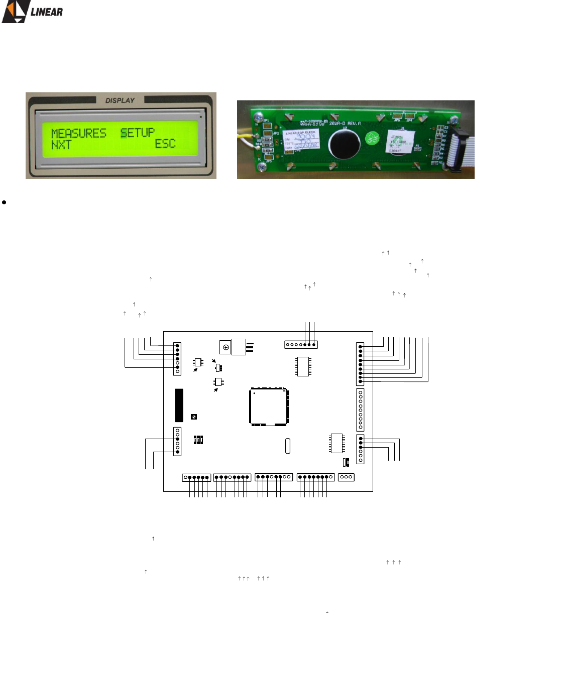
Fig.2.3 20 x 2 LCD display board - CIM3004
CIP8231 Connections
(BK) SW2 PIN 3 –CON 6 –CIP8388 –MOD. 4492 –UHF UPCONVERTER
(GR) TEMPERATURE ALARM PIN 4 –CON-5 –CIP8209 –MOD.4408 –UHF AMPLIFIER
(GY) RESTART PIN 6 –CON-8 –CIP8111 –MOD. 4401 –POWER SUPPLY
CON-1
BL
7
CON-2
1 9
9
1
3
6CON-7 CON-8 CON-9
1
GND
VCC
DA1
DA2
+15V
IRQ
CON-3
1
6
CON-4
8
CON-5
8
1
CON-6
8
1
PA21
PA31
PA41
PA51
PA61
PA71
1
PA02
PA12
PA22
PA32
PA42
PA52
PA62
PA72
PB01
PB11
PB21
PB31
PB41
PB51
PB61
PB71
PB72
PB62
PB52
PB42
PB32
PB22
PB12
PB02
GND
TX
RX
PC6
PC5
GND
A16
A15
A14
A13
A12
A11
A10
A09
GND
A08
A07
A06
A05
A04
A03
A02
A01
CI -7
LM7805
CI-1
1 2 3
TPO-1
AJUSTE
LUM. DISPLAY
XTAL1
1
14
SCL
SDA
PM4
PM3
PJ1
PJ0
16MHz DTR
CTS
RX
TX
GND
RTS
DCD
CON-11
1
6
CON-10
1
7
J1 VM
BDM IN
MC34064
LM358
CI -4
MCS12A128BMCS12A128B
MC9S12A128B
Q1
BCX53
CON-12
1
1
.
DS229
..
RS232
RS485
J4
J5
.
DS229
CI -6
CI-2
.
CI-3
.
(GY) DATA PLL PIN 6 –CON-3 –CIP8388 –MOD. 4492 –UHF UPCONVERTER
A
B
GND
(WH) RX RS232 PIN 2 –CON DB9 RS232 –REAR PANEL
(RD) TX RS232 PIN 3 –CON DB9 RS232 –REAR PANEL
(SH) GND RS232 PIN 5 –CON DB9 RS232 –REAR PANEL
(WH) GND PIN 1 –CON-6 –CIP8388 –MOD. 4492 –UHF UPCONVERTER
(BL) +15V PIN 1 –CON-13 –CIP8111 –MOD. 4401 –POWER SUPPLY
(GR) +8V PIN 1 –CON-11 –CIP8111 –MOD. 4401 –POWER SUPPLY
(YL) ENABLE QDAC PIN 8 –CON 6 –CIP8388 –MOD.4492 –UHF UPCONVERTER
(GY) SW1 PIN 4 –CON 6 –CIP8388 –MOD.4492 –UHF UPCONVERTER
(OR) CLOCK DAC PIN 7 –CON-6 –CIP8388 –MOD.4492 –UHF UPCONVERTER
(OR) LD CLOCK GENERATOR PIN 1 –CON-7 –CIP8358 –MOD. 4549 –8VSB MODULATOR
(BK) DATA OUT PIN 3 –CON-2 –CIP8357 –MOD. 4549 –8VSB MODULATOR
(BR) ENABLE PLL PIN 5 –CON-3 –CIP8388 –MOD. 4492 –UHF UPCONVERTER
(YL) CLOCK PLL PIN 7 –CON-3 –CIP8388 –MOD. 4492 –UHF UPCONVERTER
(VL) LOCK DETECT PIN 8 –CON-3 –CIP8388 –MOD. 4492 –UHF UPCONVERTER
(OR) DATA IN PIN 2 –CON-2 –CIP8357 –MOD.4549 –8VSB MODULATOR
(RD) MODULATOR CLOCK PIN 4 –CON-2 –CIP8357 –MOD.4549 –8VSB MODULATOR
(GR) MODULATOR ENABLE PIN 5 –CON-2 –CIP8357 –MOD.4549 –8VSB MODULATOR
(VL) MODULATOR READ PIN 6 –CON-2 –CIP8357 –MOD.4549 –8VSB MODULATOR
(VL) DATA DAC PIN 6 –CON-6 –CIP8388 –MOD.4492 –UHF UPCONVERTER
(YL) TX ON PIN 3 –CON DB9 –REAR PANEL
(RD) ENABLE IDAC PIN 9 –CON 6 –CIP8388 –MOD. 4492 –UHF UPCONVERTER
(YL) BACK LIGHT DISPLAY POINT A –LCD DISPLAY–CIM3004
(YL) CS MEMORY PIN 4 –CON-2 –CIP8437 –MEMORY INTERFACE
(YL) ROW1_KEYBOARD PIN 1 –CON-3 –CIP8002 –KEYBOARD
(BL) LINE1_KEYBOARD PIN 6 –CON-3 –CIP8002 –KEYBOARD
(GY) ROW3_KEYBOARD PIN 3 –CON-3 –CIP8002 –KEYBOARD
(OR) DCLK_MEM PIN 6 –CON-2 –CIP8437 –MEMORY INTERFACE
(OR) LINE3_KEYBOARD PIN 4 –CON-3 –CIP8002 –KEYBOARD
(WH / RD) ALC PIN 2 –CON-6 –CIP8388 –MOD. 4492 –UHF UPCONVERTER
(RD) ASDI_MEM PIN 5 –CON-2 –CIP8437 –MEMORY INTERFACE
(VL) DATA_MEM PIN 3 –CON -2–CIP8437 –MEMORY INTERFACE
(RD) +32V OUTPUT VOLTAGE READING PIN 5 –CON-8 –CIP8111 –MOD. 4401 –POWER SUPPLY
(OR) +32V OUTPUT CURRENT READING PIN 1 –CON-7 –CIP8111 –MOD. 4401 –POWER SUPPLY
(BL) +15V READING PIN 2 –CON-8 –CIP8111 –MOD. 4401 –POWER SUPPLY
(BR) TEMPERATURE READING PIN 5 –CON-6 –CIP8388 –MOD. 4492 –UHF UPCONVERTER
(BL) FORWARD POWER READING PIN 1 –CON-5 –MOD. 4408 –UHF AMPLIFIER
(WH) GND INPUT EXTERNAL PIN 5 –CON-DB09 –PANEL
(GY) REFLECTED POWER READING PIN 2 –CON-5 –MOD. 4408 –UHF AMPLIFIER
(GR) +8V READING PIN 1 –CON-8 –CIP8111 –MOD. 4401 –POWER SUPPLY
(BK) -15V READING PIN 3 –CON-8 –CIP8111 –MOD. 4401 –POWER SUPPLY
(BK) LINE2_KEYBOARD PIN 5 –CON-3 –CIP8002 –KEYBOARD
(BR) ROW2_KEYBOARD PIN 2 –CON-3 –CIP8002 –KEYBOARD
Fig.2.4: CIP8231- the control unit board - components and connections.

AT725P Owner’s Manual
© 2009 Linear Industries, Inc. All Rights Reserved AT725P_OM_08/09 16/75
The function of the CIP8231 board can be described in the following parts:
➢ The integrated circuit CI-4 (A128) is a 16 bit microcontroller programmed to perform the
total management functions of the equipment. This component is programmed in the factory
by a numeral designation and its current associated software version. The software version
corresponds to any updates that the control software may receive in the future for the
CIP8231 board.
➢ The analogical readings function: All available analogical readings are sent via the connector
CON-9 on the CIP8231 board. Analogical readings include the following parameters:
• Direct power – 25W Amplifier.
• Reverse power - 25W Amplifier.
• (+9V) - Power supply.
• (+18V) - Power supply.
• (-18V) - Power supply.
• (+32V) - Power supply.
• (I1) – the main power supply drain electrical current.
All these seven analogical information are sent to microcontroller CI-4, where they are first
digitalized and then processed. The software of this microcontroller establishes that the nominal
value of the readings is 4Volts, that is, in connector CON-9 the reading information will have to
be of 4V in the way to express nominal values of each readings at the LCD display located at
the front panel of the equipment.
On each module of the equipment that generates some type of control-analogical information,
there is an associated test point. When during the calibration process external instruments
measurements indicate the correct nominal value for that function, a trimmer is adjusted in such
way that the voltage on the test point is set on +4Volts.
On the test point associated with reflected power, if the voltage becomes higher than +4Volts,
the control unit will process this event as an alarm. This will occur every time that the reverse
power exceeds 10% of the direct power.
Alarm detection
In case of substitution of the CI-4 or even the entire PCB CIP8231, it is mandatory to
inform the factory prior replacement, the programming identification number that is
clearly indicated at the CI-4 body.

AT725P Owner’s Manual
© 2009 Linear Industries, Inc. All Rights Reserved AT725P_OM_08/09 17/75
For the listed alarms below, the CIP8231 control unit board shuts down the transmission by
making the ALC voltage 0Volts at the up-converter module, 4492. For more details see the
power control description on the next page.
The possible alarms to be interpreted by the CIP8231 are:
• Lack of lock voltage of the PLL at the Up-converter - Module 4492.
• Excessive temperature of the 25W UHF amplifier - Module 4408 – (above 65ºC).
• Excessive reverse power (above +4V at CON-9).
• Overflow of the FIFO in the 8VSB modulator (informing for communication between
microcontroller and modulator).
• Lack of synchronism of the transport stream, MPEG.
• Presence of not programmed hardware (it can appear in the warm-up phase of the
equipment).
• Imperfections associated with the generation of the master clock signal in the
modulator 8VSB - Module 4549.
The alarms above reach the connectors CON-4, CON-5 and CON-6 at the CIP8231 board as
digital information.
The microcontroller (CI-4) receives the alarm(s) information, processes them into the system,
and the software makes the decision to incapacitate the transmission or not.
The presence of +5V in the pins of alarm of connectors CON-4 and CON-6 and, therefore, in
connector CON-5 means that the status of alarms is empty and the transmitter operates
normally. In the event of one of these points of alarm falls for a value below of +5V, being
generally the zero, the microcontroller inhibits the transmission.
The alarms generated in the system are displayed as - alarms - in the Master Control Unit
window (MCU) on the front of the AT650P. The corresponding identification symbol of alarms is
“*” for current alarms - CURRENT - or “#” for old alarms - PAST. In the occurrence of an alarm
“*” in Alarms the transmission automatically will be inhibited. When the causing problem of the
identified alarm “*” is resolved, the “#” symbol will appear and the transmission will return
(slowly) to its full power. To erase old alarm records, key “CLR.ALL” in the MCU panel of the
AT725P, or in the hyper-terminal (keyboard key “1”).
Communication with 8VSB modulator
The CIP8231 board makes the communication with the 8VSB modulator - Module 4549 -
through a set of serial interface gates, (SPI). These connections are present on the pins 2 to 5
on the connector CON-3 and also on pins 5 and 6 of CON-5 connector.

AT725P Owner’s Manual
© 2009 Linear Industries, Inc. All Rights Reserved AT725P_OM_08/09 18/75
The communication between the CIP8231 board and the 8VSB modulator module 4549 has the
objective to make the reading and the configuration of determined parameters of this module, as
for example, the adjustment of the pilot programming stream, or the 8VSB signal, and
adjustment of the rejection of superior lateral band.
Setting the FCC/UHF operational channel
The programming of operational channel of the equipment is made on the CIP8231board. Out
from this board the generated channel code will program the up-converter - Module 4492 - for
one determined UHF canal of/ATSC. This stream of information is composed by data, clock,
and enabling code, and are present at pins 1, 2 and 3 of CON-4 connector on CIP8231 board.
The control board sends the right channel operational information to program de fraction-base
PLL circuit at CIP8388, which will synthesize the local oscillator frequency suitable for the
desired channel.
All time that the equipment is turned on, the CIP8231 board automatically makes the
programming of the PLL at the module 4492.
It is important to remember that the initial programming that CIP8231board sets for the exciter
AT725P is made in the up converter is factory procedures. These programming procedures are
made in the act of the configuration of the equipment and although to be done it saw panel
frontal (keypad and display), they are not accessible to the end user.
In turn, the module 4492 sends to CIP8231 board, the lock detected information, as response
that the PLL circuitry is in lock and ready for operation. This information is packaged as voltage
level of approximately of +3,6V and is routed to the pin 5 of CON-4 connector CON-4 on the
CIP8231 board. The absence of this voltage will trigger the lock alarm that will cause the
reduction to 0 of the RF power of the module and at the same time will be signaled in the LCD
display located in the front panel of the exciter.
RF power control
The programming of transmitted power made by the end user, and can be made via the front
panel. The CIP8231 board converts this digital input programming information into analogical
level of voltage. This voltage is then sent to the up converter of the exciter. This specific voltage
level is called as ALC REFERENCE VOLTAGE or trellis voltage, being shown in the LCD digital
display as V.P. Adj.
The trellis voltage is directly proportional to the RF power level at the output the exciter, that is,
higher the trellis voltage higher the exciter RF power level. The typical value of trellis voltage
when the transmission is under the normal rated power is between 3V and 4V.

AT725P Owner’s Manual
© 2009 Linear Industries, Inc. All Rights Reserved AT725P_OM_08/09 19/75
For some failures, or malfunctions, the power control is responsible for the immediate action to
reduce to zero the RF power level of transmission that is, zeroing the trellis voltage, in the
following situations:
• Lack of Lock of the PLL of the UP Converter - Module 4492.
• Temperature of the UHF Amplifier of - Module 4408 - above 65°C
• Imperfection in the generation of master clock in the 8VSB modulator - Module 4549.
When the equipment is turned on and the warm up period starts, around 5 seconds, the exciter
reaches the nominal RF power value. This period of time, is also known as SLOPE UP time, it is
the time necessary for the trellis voltage increases from its initial 0V up to its the corresponding
value to set the programmed RF power level at the output of the exciter.
Programming the off-set operational frequency
The AT725P exciter is factory adjusted in a given FCC/UHF operational channel, under ATSC
standard 8VSB modulation process, and no off-set is set. This channel can or not suffers
change in its off-set frequency, under the end user discretion. The offset can shift the RF
channel band up to 30 kHz, in 1Hz increments. The shift of frequency can increase or decrease
the start frequency of the band of the UHF channel. The offset is programmed at the CIP8231
board, and acts at the up-converter module 4492, on the pins 1, 2, 3 at CON-4 connector.
All time that the equipment is turned on, the CIP8231 board automatically re-confirms the last
set of programmed data at the 4492 up-converter module. It is important to say that
programming instructions generated by the CIP8231 board of the exciter are initially set via the
keypad/LCD screen located on the front panel of the exciter. However, those are procedures set
on the factory and, therefore, not accessible to the user.
+32V power supply ON/OFF control.
The CIP8231 board sends to the power supply, module 4401, a command to switch it ON. It is a
+5V level command. It is present at pin 6 on CON-3 connector.
The absence of this command voltage will make that the power supply module 4401 stops to
supply the switched +32V line, which feeds the 25W UHF amplifier module 4408. The others
voltages generated by other power supplies are always present during the exciter operation.
Serial communication RS232
The access to CIP8231 board is possible made through a PC that has the Windows Hyper
Terminal. Located on the rear panel of the exciter there is a DB9 connector tag as RS232.

AT725P Owner’s Manual
© 2009 Linear Industries, Inc. All Rights Reserved AT725P_OM_08/09 20/75
This connector is linked to connector printed circuit connector CON-10, located at CIP8231
board.
Keypad – CIP8002 board
The CIP8002 board contains five key bottoms SW1 to SW5, located on the front panel of the
exciter. This board is a matrix of electrical ON/OFF contacts. The responses are made available
at the CON-3 connector.
LCD - CIM3004 board
CIM3004 board is a LCD - Liquid Crystal Display - of 20 columns for 02 lines. The luminosity of
deep (back light) of this display is made by CIP8231 board that sends +5V between the test
point termed A+ (yellow wire) and ground test point termed K- (white wire). The multi-way
connector CON-2 receives the pin-to-pin from the CIP8231 board. The trimmer TPO-1 present
at CIP8231 board controls the intensity of the characters of the display and the jumper J1, also
present at CIP8231 board, must be set on the R61 position, if is desirable that the LCD back
light stays ON all time.
AT725P Owner’s Manual
© 2009 Linear Industries, Inc. All Rights Reserved AT725P_OM_08/09 21/75
Section 3 – 8VSB Modulator and Master Clock
Module 4549
Introduction
The Module 4549 is composed by an 8VSB MODULATOR including an IF pre-correction circuitry CIP8357
board (CIM3510) and also a MASTER CLOCK UNIT, CIP8358.
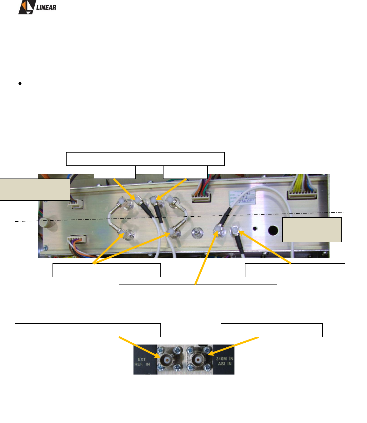
Each one of these printed circuit boards are located below of one out of the two lateral covers of module
4549, as it shows the drawing of external connections of this module.
(a)
(b)
Fig.3.1: Module 4549, (a) top view, (b) connectors, from rear panel
Internal 10MHz TCXO ref. input
10MHz OCXO ref. output to Up Converter
172MHz Master Clock
8VSB IF Modulated - 18.8339 MHz
IF (I) carrier
IF (Q) carrier
8VSB Modulator
Section
Master Clock
Section
Transport Stream Input
10MHz External Reference Input
AT725P Owner’s Manual
© 2009 Linear Industries, Inc. All Rights Reserved AT725P_OM_08/09 22/75
General Functional Description
The module 4549 can be break down in 2 printed circuit boards. This section describes the 8VSB modulator
only. These boards are physically located below of each side of the top covers, as shown on the figure
below:
CIP8412 board - 8VSB Modulator/Pre-corrector.
The CIP8412 is part of the Module 4549. It is the 8VSB modulator that process the transport stream (TS) that
carries up to 4 broadcast programming including, audio, video and data. All information compressed and
multiplexed in a MPEG2 format.
Fig.3.2: CIP8412 – 8VSB Modulator Block Diagram
The 8VSB channel modulator inserts the forward error correction, (FEC), into the transport stream MPEG2.
The modulator follows the ATSC standard A/53 annex D.
CIP8412 board - general functional description
The input transport stream signal to be modulated must be either ASI or SMPTE310M format at with
19.39Mbps of bit rate, and with 800mVpp @ 75 ohms. The ASI/SMPTE 310M input is located on the rear
panel by a BNC connector.
First the circuit to recover the clock rate is used to perform the protocol interface. After that there is a rate
equalization of the transport stream, TS, performed by the insertion or delete of the null packets, at the end
the symbol rate is ready to be stabilized and locked with a external/local reference of 10MHz and no longer
with the TS stream that is limited to 2.8ppm accuracy. During this processing is also used the re-stamping
for multiple programs, termed as PCR.

AT725P Owner’s Manual
© 2009 Linear Industries, Inc. All Rights Reserved AT725P_OM_08/09 23/75
The entire 8VSB modulation process is digital. This process includes the FIR filters, and do not uses SAW
filters to create the VSB band. Digital modulation increase the quality of the modulated signal measured via
a proportional increase of the MER, (Modulation Error Rate). The modulation process generates 2 identical
but orthogonal signals, termed signals; I and Q. The frequency of the IF carrier is 21.52MHz, and the center
of the channel is 18.8MHz.
The value for the system when working with 2 orthogonal carriers is because it is possible to implement
corrections on non-linear distortions, or simply implement digital pre-distortion. The digital pre-correction is
possible using LUT, (Look up Tables) refer to Section 7. This table synthesizes inverted responses regarding
the RF power amplifier transfer function, reducing the IMD products.
The digital processing generates I and Q distorted, and these 2 signals are then converted to the analog
format via a 16 bits DAC, with 2 balanced outputs, on a total of 4 output analog signals. These signals are
termed; I, I’, Q and Q’, and are respectively present at the CN9, CN8, CN6, and CN5 connectors at CIM3444.
These 4 signals will become the UHF Up-Converter input signals, Module 4453.
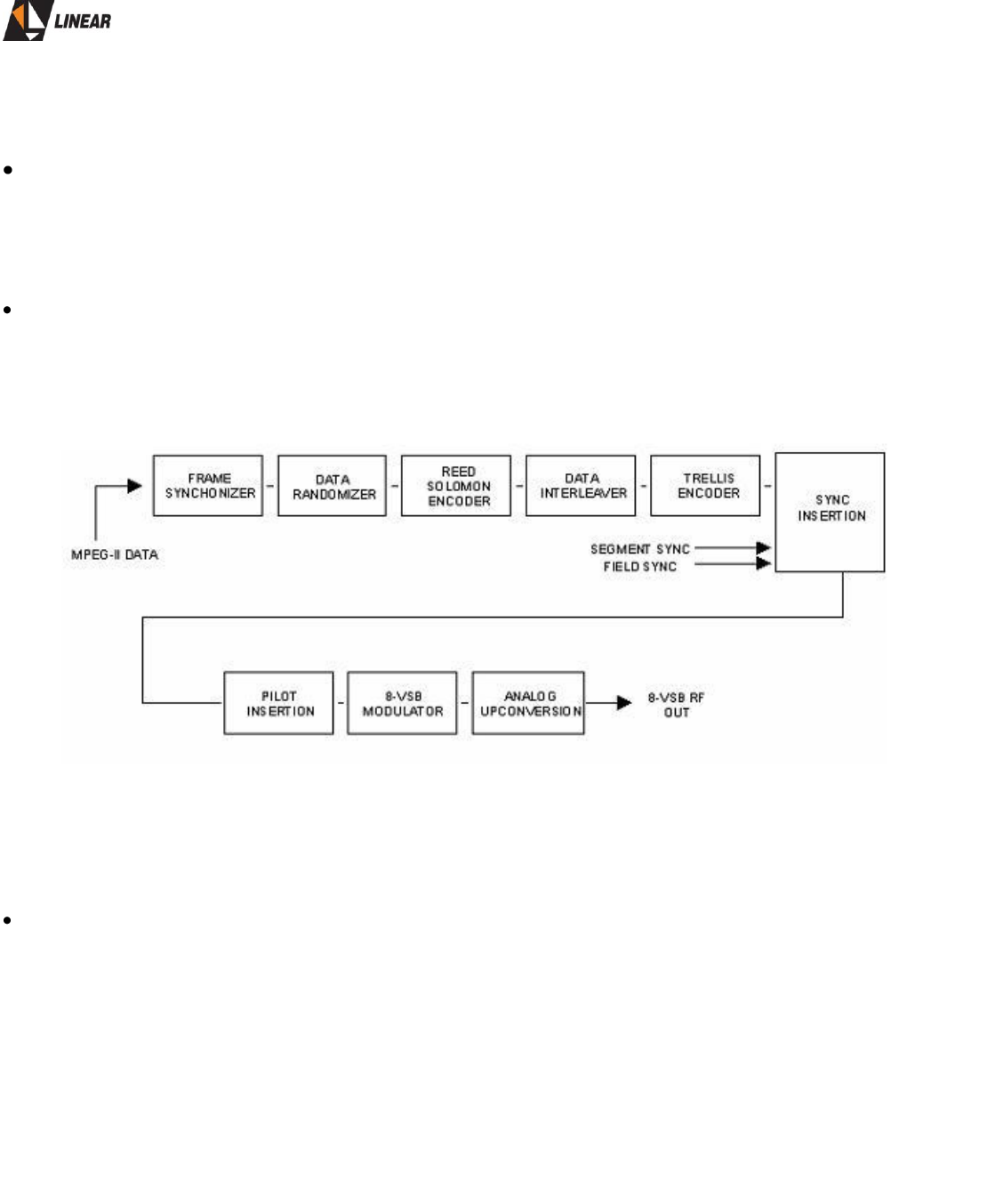
After the data processing as described below, the data stream is ready to receive the channel coding, that is
break down on the following steps:
Frame synchronization:
For each 188 bytes on the MPEG2 package, this circuit identifies and removes the 47th byte.
Randomizer:
This circuit equally spread the modulated signal energy over the channel band. The final energy density is
similar to a AWGN noise, with this technique, it is possible to achieve a higher bandwidth usage efficiency.
Reed-Solomom:
Reed-Solomon is a block coder, (207,187) that adds 20 redundant bytes on each 187 bytes of the MPEG2
package. With this method it is possible to correct on the reception site, some possible data errors that may
had occurred during the transmission of the RF signal.
Interleaving:
The interleaving technique helps to spread the errors around the time line, making them even less
susceptible to burst errors.
Trellis Code:
Trellis code is closely related to the channel modulation. It is a convolution coder using 2/3 rate, meaning for
each 2 bits at the input, there are 3 coded bits at the output creating the 8 symbols used on the 8VSB
modulation process, (-7, -5, -3, -1, +1, +3, +5, +7), having as ultimate goal improve the threshold on the
signal-to-noise ratio of the system.
AT725P Owner’s Manual
© 2009 Linear Industries, Inc. All Rights Reserved AT725P_OM_08/09 24/75
Synchronism Insertion:
The synchronism insertion built the symbol overall structure, creating the fields and frames as specified on
the A/53E standard.
Pilot Insertion:
This part of the circuit adds a small DC level into the carrier to allow a safer and robust reception of the
signal. This DC level is equivalent to 1.25 CU (Constellation Units).
Master Clock – CIP 8358 board – (CIM 3445)
Introduction
The CIP8358 board, embedded into the module 4549, out from a 10MHz internal/external reference signal,
synthesizes a 172.16MHz oscillator that represents 16 times the symbol rate of the modulator 8VSB.
This oscillator signal is squared by a Schmitt-trigger circuit with amplitude equal to 0-3.3 volts. This square
wave type signal is the master clock signal that will synchronizes all the digital circuits on this equipment
except the control signals.
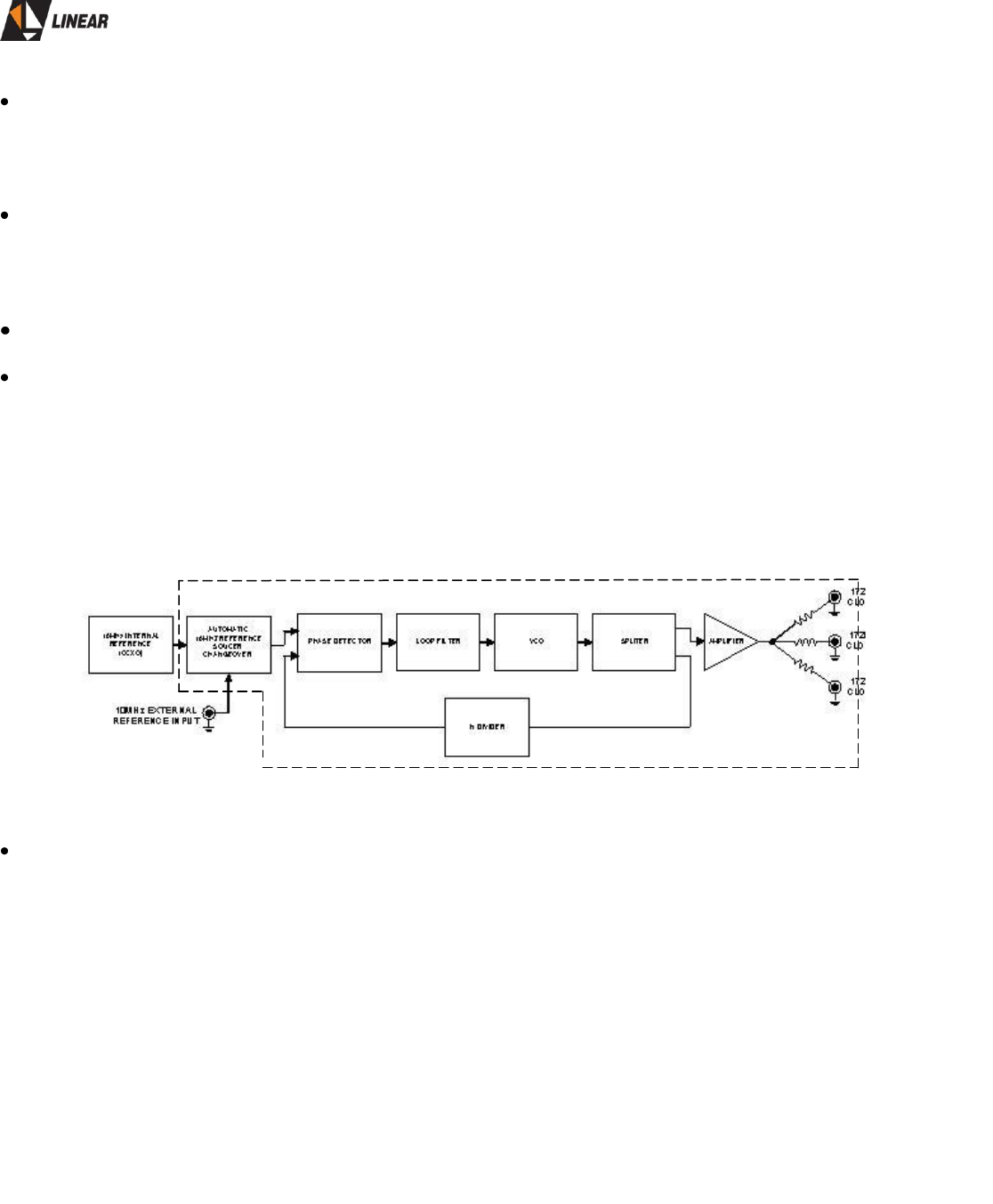
Fig.3.3: CIP8358 master clock – block diagram
CIP8358 board – general functional description:
The 172.16MHz frequency is synthesized via a PLL, a VCO and a DDS circuit. The 10MHz reference is one
out of the two inputs of the phase comparator. This signal comes to CIP8358 via a SMB connector, CON-1.
The second input is also a 10MHz generated by the DDS circuit out from the free running 172.16MHz
oscillator.
The loop filter performs the integration of the phase comparator output, generating the error signal that is
feed back to the VCO. On this way the VCO is locked to the external reference signal.
The oscillator signal is delivery via 3 connectors located on the CIP8358 board. Two of those signals are
routed to the 8VSB Modulator, CIM3510 board.
AT725P Owner’s Manual
© 2009 Linear Industries, Inc. All Rights Reserved AT725P_OM_08/09 25/75
Section 4 – IF/UHF Up-Converter
Module 4492
Introduction
The module 4492 performs the basic functions:
This module translates the incoming I and Q IF carries, from the 8VSB modulator, to a desirable
FCC/UHF operational channel.
Controls the RF output power of the exciter.
The desirable channel configuration is defined via the keypad and the LCD display on the factory. Channel
changes are not allowed to the end user.
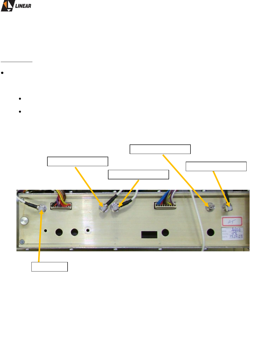
Fig.4.1: Module 4492, RF connections.
RF Output
Ref. 10MHz input
2 x LO sample
(Q) IF input
(I) IF input
AT725P Owner’s Manual
© 2009 Linear Industries, Inc. All Rights Reserved AT725P_OM_08/09 26/75
The main features associated with this module are:
Simple conversion.
Orthogonal mixing, that perform the image rejection, and LO rejection.
Synthesized local oscillator via PLL, 22 bits serial fractional.
Allow channel programming @ 1Hz resolution when using GPS reference.
The LO frequency is divided by 2, that insures 6dB improvement on the LO phase noise.
10MHz internal reference oscillator, technology OCXO, (Oven Controlled Crystal Oscillator).
Uses hybrid amplifiers with high linearity.
Overdrive protection circuit, acts maintaining the RF power via power reduction.
Automatically reduces the exciter RF output power in absence of IF signal, either Q or I carriers.
Stand-by for local oscillator, in case of some failure on the external reference signal.
Meet or exceed the phase noise requirements for DTV transmission.
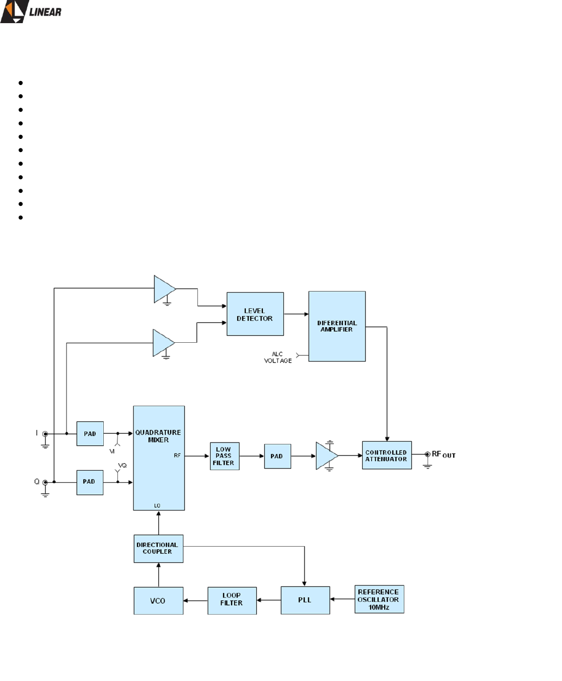
Module 4492 - General functional description - Refer to Fig.4.2.
Fig.4.2: Module 4492 – block diagram
AT725P Owner’s Manual
© 2009 Linear Industries, Inc. All Rights Reserved AT725P_OM_08/09 27/75
The already modulated IF carrier I and Q feed the 2 inputs of the up converter 4492 module. The output
signal of this module is a FCC/6MHz/UHF channel (14-69). Besides this main function, it also controls the
potential overdrive into the final 25W amplifier.
The up-conversion circuit consists of an orthogonal mixer fed by the 2 orthogonal IF carriers, I and Q fixed
center frequency and 6MHz bandwidth. The mixer bit the IF signal with the suitable local oscillator CW signal.
The result is two RF lateral bands. The superior lateral band is not desirable and is attenuated by 35dB.
The resultant RF signal is filtered and amplified. The serial data stream that program the PLL circuit are
transferred via MICROWIRE interface, composed by 3 high speed transfer lines, 20MHz. The
microcontrollers inside the up-converter perform the following function controlling the up-converter:
PCB CIM3443 – Local Oscillator:
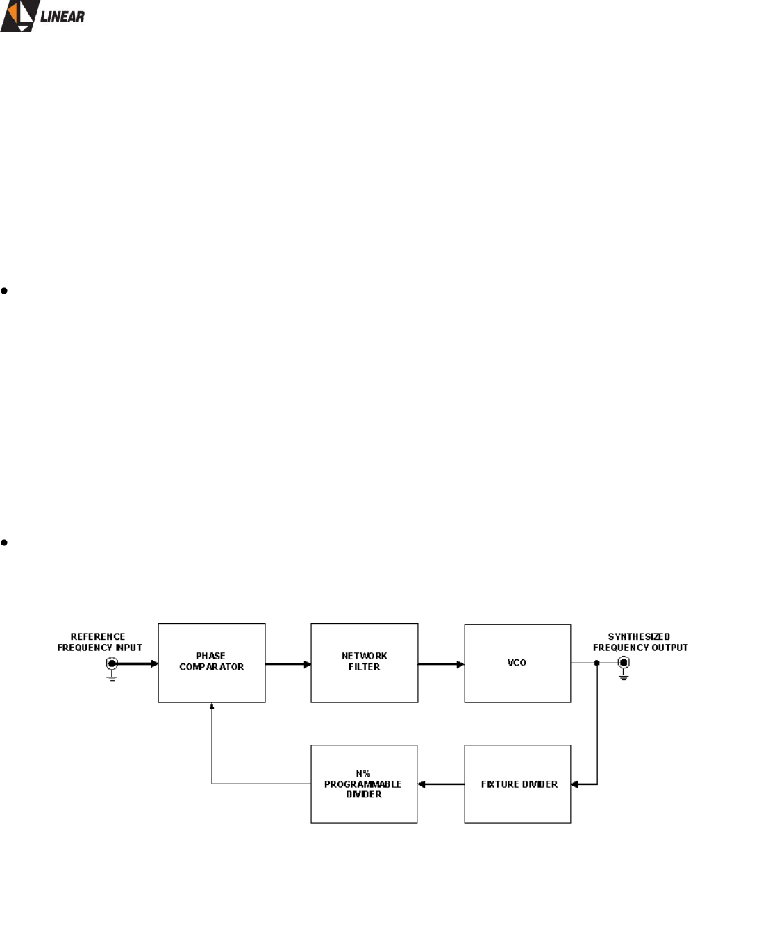
The local oscillator is designed based on a PLL circuit. This oscillator is able to synthesize frequencies within
the band from 450MHz up to 900MHz. To guarantee a high quality signal generation out from the local
oscillator, 4 VCO’s (voltage controlled oscillator) were implemented with a shift frequency range of 125MHz
each. Just one VCO works at the time to avoid interferences. On this arrangement, a 102dBc@20Hz phase
noise is achieved. The synthesizer on the feedback loop select the desired frequency inside the choose VCO
band.
The VCO’s signal outputs are isolated among them via a sum and inverted circuits. The reference frequency
generated by a DDS circuitry complete the Up-conversion frequency process. The output local oscillator
signal power is +5dBm.
PCB CIM3443 – Local Oscillator – block diagram:
Fig.4.3: CIM3443 local oscillator – block diagram
AT725P Owner’s Manual
© 2009 Linear Industries, Inc. All Rights Reserved AT725P_OM_08/09 28/75
PCB CIM3442 – UHF Mixer
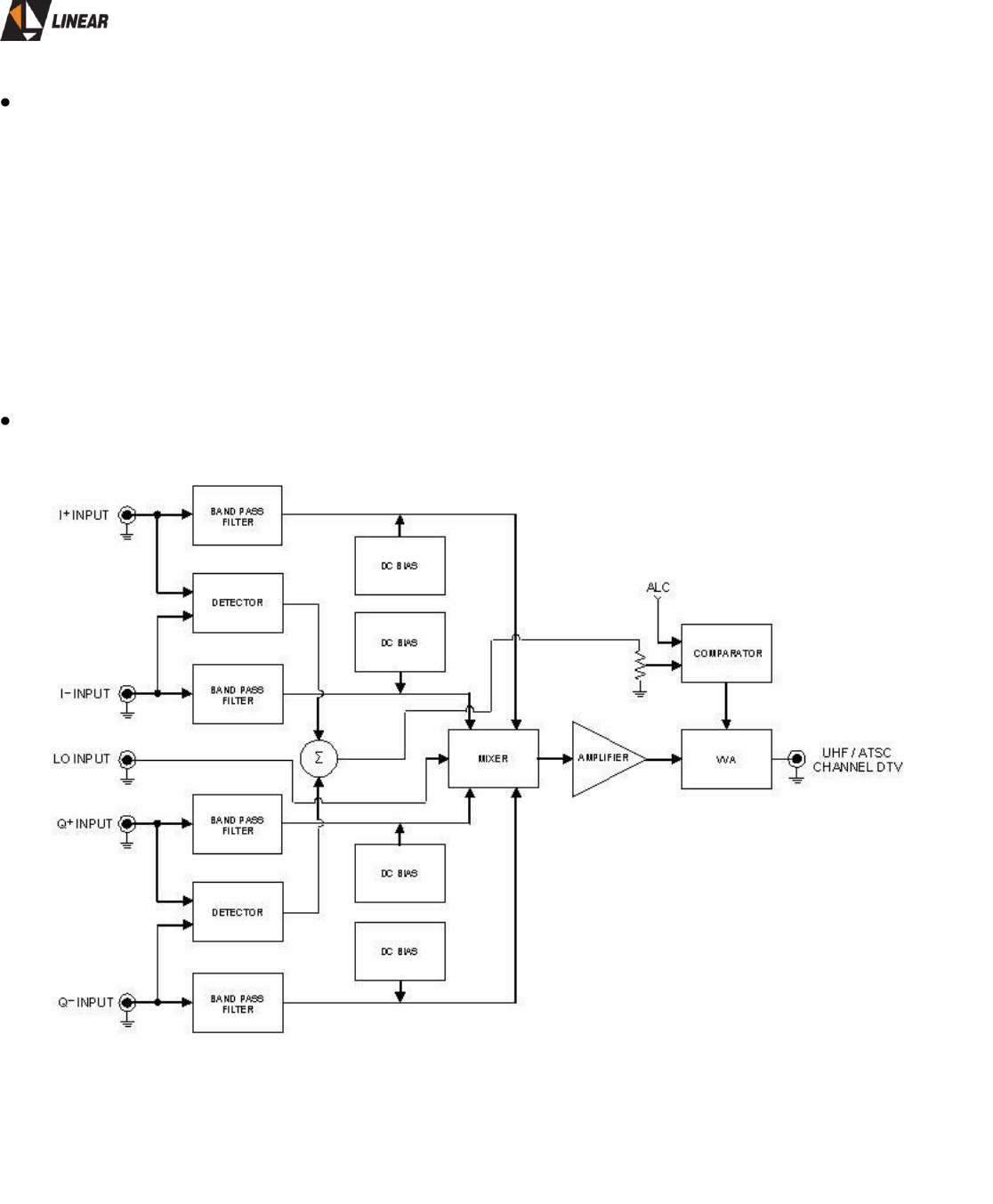
The mixing operation translates the IF modulated signal frequency up to the assigned UHF broadcasting
channel, the operation utilizes the complex approach considering the orthogonal pair of signals (I-, I+) and
(Q-,Q+) allowing rejection of one side band, and the oscillator itself. The rejection is around 40dB, facilitating
the post filtering steps.
Right after the mixing operation, the now RF signal is 10dB broadband (VHF and UHF) amplified under a
typical 2dB roll-off characteristic. The RF output pass through a 25dB dynamic range variable attenuator.
The control of this attenuator is related with the DC level generated by the ALC (Automatic Level Control). In
case of absence of a IF signal or valid IF signal (locked via PLL) of any of the 4 possible IF signals, the
attenuator assumes it higher level of attenuation, and shutting down the RF chain of amplification.
PCB CIM3442 – UHF Mixer – block diagram
Fig.4.4: CIM3442 UHF mixer – block diagram
AT725P Owner’s Manual
© 2009 Linear Industries, Inc. All Rights Reserved AT725P_OM_08/09 29/75
PCB CIM3442 – UHF Mixer – adjustment procedures:
The mixer-ALC circuitries have 2 types of adjustments. The first one is a DC level that polarizes each
branch of the input of the complex mixer. Each one of the DC levels must be adjusted seeking for the max
rejection on the un-desired vestigial side band, in conjunction with the LO rejection as well. The level
adjustments are performed by the trim pots: TPO-1, TPO-2, TPO-3, and TPO-4. Voltage range of +1.4V to
+1.6V should be present on the following test points.
TPO-1: readings on L17
TPO-2: readings on L18
TPO-3: readings on L19
TPO-4: readings on L20
The second set of adjustments follows the first one. Once the first set is completed, the fine tuning
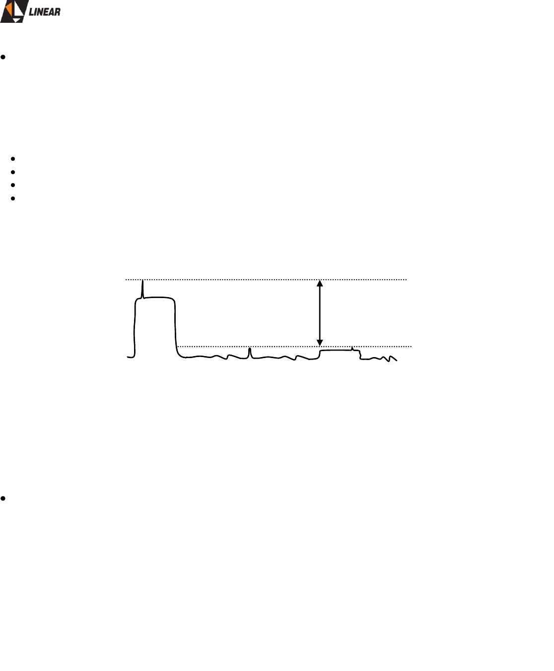
adjustment should be performed. It is necessary to connect the spectrum analyzer to the UHF RF output of
the sub-module 4453. At this point, either the LO signal, as the superior RF spectral image of the UHF/ATSC
RF channel, must be attenuated by 40dBc.
40dBc
UHF / ATSC
CHANNEL DTV
(BELOW MIXING)
LOCAL OSCILATOR
SIGNAL
UHF / ATSC
CHANNEL DTV
(ABOVE MIXING)
40dBc
UHF / ATSC
CHANNEL DTV
(BELOW MIXING)
LOCAL OSCILATOR
SIGNAL
UHF / ATSC
CHANNEL DTV
(ABOVE MIXING)
Fig.4.4: Level references for mixer-ALC fine tuning
The second adjust detects the protection signal at the center of the band. In absence of 1 out of 4
controls IF signals, this DC level exceed the min threshold and shut down the RF output signal. The DC
threshold adjust is performed by TPO-5, and should be set for +2.5V.
Module 4466 – Direct Digital Synthesizer (DDS)
The module 4466 is a signal reference generator based on a DDS circuit. This module is able to
synthesize frequencies up to 50MHz under mHertz precision range. The signal is used as PLL reference on
the UHF Up-Converter module 4453 – PCB CIM3442. The RF channel 10kHz off-set if necessary, is pre-set
on the DDS circuitry. The phase noise on the reference signal generated on this module is better than
110dBc/Hz.
The SCU unit – PCB CIM3297 – configures the DDS’s circuitry parameters via a serial
communication port. The DDS module receives a signal out from the master clock module 4454 - PCB
CIM3445; perform the programming operation for the RF output channel as required under mHertz precision.
At the end, is expected a frequency error around 1Hz max., when measured at the output of the UHF mixer
circuit. Before leaves the module, the DDS signal is amplified and filtered.
AT725P Owner’s Manual
© 2009 Linear Industries, Inc. All Rights Reserved AT725P_OM_08/09 30/75
Section 5 – 25W UHF Multistage Amplifier
Module 4408
General Functional Description
Introduction
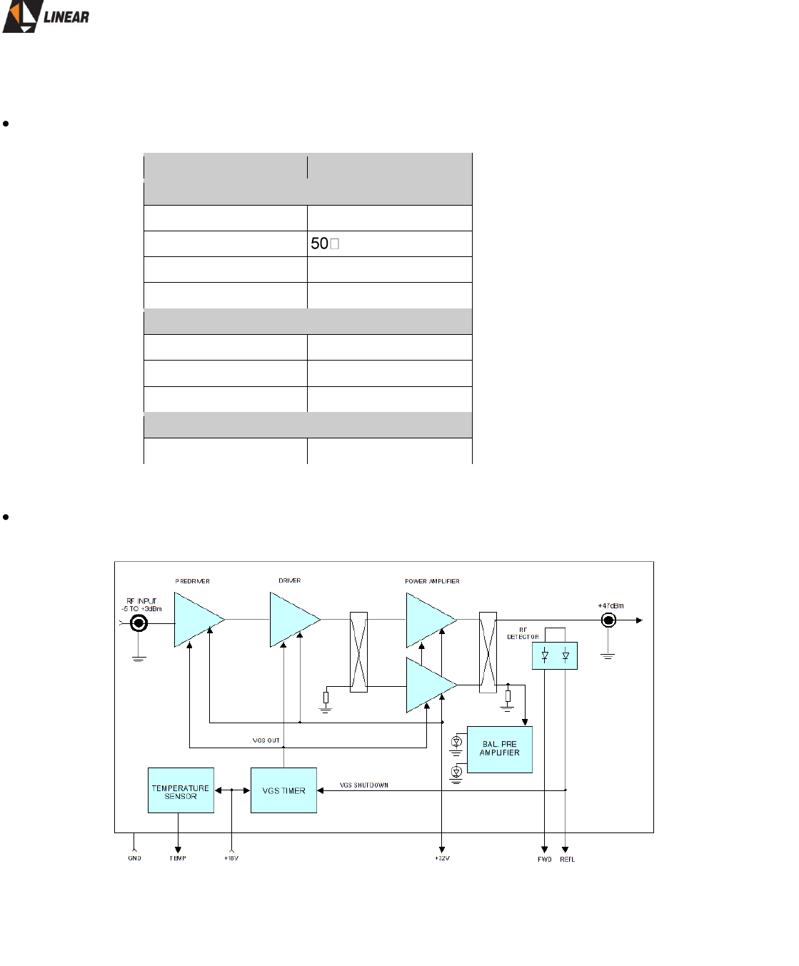
The module 4408 was developed to act as driver of DTV in standard ATSC in all the band of UHF. It is
composed by three stages of amplification. The module 4408 has high linearity with a satisfactory
performance for TV signals. This module was developed to operate in three bands of UHF, which are:
• LOW BAND (LB): channels 14 to 44
• HIGH BAND (MB): channels 45 to 59
For the two bands of UHF described above, the same PCB is used.
25W UHF / ATSC AMPLIFIER - MODULE 4408
CIRCUIT
CIM
CIP
DRIVER
3392B
8209
What defines which one UHF band the module 4408 must operate, are determined by the PCB’s
components.
Module 4408 is divided in the following parts:
3dB input attenuator, (3dB PAD)
This attenuator is composed by 3 resistors connected as type π topology, R1, R2 and R3, this attenuation
guarantee 6 dB isolation. The input matching circuit also has 4dB isolation. The total isolation between the
PCB input and gate of the transistor T1, is at least 10dB.
First amplifier on class A
This section uses the transistor LDMOS, T1 (PD57006) with operating with a power gain close to 22dB. The
class A polarization insures a high linearity amplification behavior.
The transistor T1 is connected to the +32V power supply, module 4401. This voltage is available at the pins
2, 3, 4 and 5 at the connector CON-2 – module 4408. The trimmer TPO-1 adjusts the VGS voltage of the
transistor T1 and, consequently, the drain bias current (ID) of this same transistor. By trimmer C15 the gain
of T1 is optimized for the highest value.

AT725P Owner’s Manual
© 2009 Linear Industries, Inc. All Rights Reserved AT725P_OM_08/09 31/75
Second amplifier on class A
The transistor LDMOS T2 (MRF-373) is the main device of the second amplifier on the module 4408. This
transistor also is polarized on class A. The drain voltage is gotten from +32V main power supply. This
voltage is available at pins 2, 3, 4 and 5 of connector CON-2 of module 4408. The trimmer TPO-2 adjusts
VGS voltage of T2 and, consequently, the drain bias current of (ID) of this transistor.
To trimmers C32 and C33 adjust the gain associate with T2, being optimized for the highest value.
Third amplifier on class AB
This final amplifier device is the LDMOS transistor T3 (BLF-861A) type GEMINI, that is, in the same die it has
two transistors. The polarization of T3 is made in class AB, what it guarantees higher efficiency without a
significant loss of linearity.
The +32V power supply for this amplifier is also gotten from the main power supply. This voltage is available
at the pins 1, 2, 3, 4, 5 and 6 out of the CON-3 connector of the module 4408. The trimmer TPO-3
simultaneously adjusts the VGS voltage for each one of the gates of transistor T3 and, consequently, the
drain bias current of T3.
LDMOS’s VGS voltage soft start circuit
Module 4408 is endowed with a protection system that approximately delays in 2.2 seconds the release time
of the polarization voltage VGS of the LDMOS transistors. On doing that it is guaranteeing protection against
potential undesirable voltage spikes during the transient turn on period.
The +12V voltage regulator CI-8 sees from pin 1 of the connector CON-2, the +18V voltage originated on the
main power supply module 4401. The +12V at the output of CI-8 suffers the 2.2 seconds delay caused by the
circuitry composed by the operational CI-7B, D5 diode and the soft started time constant caused by R73 and
C91 . This voltage is presented to the (+) non-inverting input (pin 3) of the op-amp CI-7A that compares that
it with the +6V threshold voltage on the (-) inverting input (pin 2). At the moment that pin 3 voltage is higher
than pin 2, the op-amps changes its state and deliver at its pin 1 +10.8V approximately. This voltage will
energize the VGS’s polarization circuits.
Temperature alarm
The module 4408 is protected against risk of over temperature operation. If the temperature raises and
exceeds 65˚C (140˚F) the protection circuit acts and disconnect the module.
The protection circuit is composed basically for the thermal sensor S1 and the CI-5. The temperature of the
module converted into a DC voltage can be measured at pin 4 at CON-5 connector. This voltage is routed to
pin 7 of CON-6 connector at the control unit PCB. The lack of this voltage means that the temperature of

AT725P Owner’s Manual
© 2009 Linear Industries, Inc. All Rights Reserved AT725P_OM_08/09 32/75
module 4408 exceeded the 650 C. Under this occurrence, the control unit will no longer allow to the +32V
power supply to feed the module.
RF Power Measurements
Through a PCB type directional coupler at CIP8209 board, a RF output sampling is collected. This RF
sampling is sent to the circuits of direct and reversed power readings. The detector circuit for direct power is
basically composed by the diode D1B, the operational amplifier CI-3B and the trimmer TPO-5 that fine
adjusts the detected DC level. The detected voltage will be displayed as RF power level on the LCD screen
on the front panel. The reverse RF power reading is performed by diode D1A, the operational CI-3A and for
trimmer TPO-4, which adjusts the level of reading measured in pin 2 of CON-5 connector.
Protection against high reverse power
In an event of reverse power at the RF output, meaning reading of RF equal or above 20% of the direct
power the reflected protection circuit will act. The action with no longer provide VGS for the LDMOS
transistors, enforcing the 0 current condition. The diode D1A detects the reversed RF power converting it into
a DC voltage. This voltage is amplified by the CI-3A op-amp, and sent to the non-inverting input (pin 5) of
comparator CI-4B where is compared with the +6V fixed voltage at the inverting input (pin 6) of this
comparator. Any time that the reverse power spike up the voltage at pin 5 above +6V the CI-4B output (pin7)
will assume a +Vcc level enforcing T5 to the saturation point. Once saturated T5, it will no longer provide any
positive voltage to pin 3 of CI-7A op-amp so, consequently, the +10.8V will no longer be present and the
VGS voltage will not be available for the transistors LDMOS. On this case the RF power is not present.
RF balancing monitor
Module 4408 has a error detector circuit for phase and amplitude unbalancing. This circuit constantly
monitors the RF output of the pair of transistors part of T3. If the phase and amplitude are not correct, the
power combination will not happen as desirable at max efficiency, excess of heating will be generated then.
Two monolithic LED will go off according with the current operational condition. If the RF power combination
is running correctly the green LED will be ON, if not than the red LED will be ON.
R30 is the dummy load for the hybrid H2. On ideal conditions, there is no RF power present on it. Under
unbalance condition, some RF power will start to be present on R30. The unbalance condition is
consequence of a less than ideal tuning of the RF network surrounding T3. In this situation D3 diode detects
this power converting it into level DC in the not inverting entrance (pin3) of the DC amplifier CI-4A, causing
saturation into transistor T4 and, consequently, the red LED LED1 will be lighted. An ideal tuning correctly
achieved via trimmers C50, C54, C64 and C68, it will not allow any unbalanced RF power by R30 and the T4
transistor will remain cut, what it makes with that the green LED - LED2 be lighted.
AT725P Owner’s Manual
© 2009 Linear Industries, Inc. All Rights Reserved AT725P_OM_08/09 33/75
Technical specifications
PARAMETERS
SPECS
INPUT
FREQUENCY
470 to 860MHz
IMPEDANCE
CONNECTOR
SMB MALE
RETURN LOSS
≥ 10dB
RF OUTPUT
GAIN
43dB ≤ ±2dB
ATSC RMS POWER
Up to 23W
HARMONICS 2nd
≤ -30dBc
GENERAL
CONSUMPTION
324VA
Module 4492 block diagram
Fig.5.1: 25W UHF ATSC Multistage Amplifier
AT725P Owner’s Manual
© 2009 Linear Industries, Inc. All Rights Reserved AT725P_OM_08/09 34/75
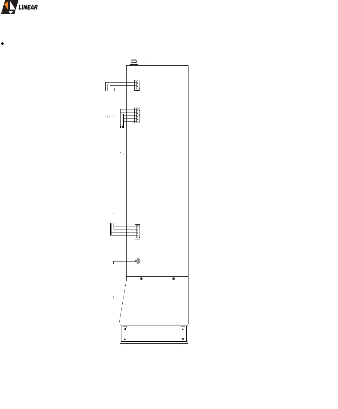
Module 4492 external connections
Fig. 5.2: 25W Amplifier – The Module
(WH) GND PIN 1 –CON9 –POWER SUPPLY
(GR) TEMPERATURE ALARM PINO 7 –CON-6 –CONTROL UNIT
(BL) +18V PIN 1 –CON13 –POWER SUPPLY
(YL) FOWARD POWER READING PIN 4 –CON9 –CONTROL UNIT
(OR) +32V RES PIN 1 –CON14 –POWER SUPPLY
(WH) GND PIN 1 –CON9 –POWER SUPPLY
(OR) +32V RES PIN 1 –CON14 –POWER SUPPLY
(WH) GND PIN 1 –CON9 –POWER SUPPLY
1 2 3 4 5 6 7 8 12 3 4 5 6 7 8
CON-1 CON-2 CON-3
CON-4
CON-5
RFIN
RFOUT
(CABLE BELDEN 50 ) INPUT RF CON-4 –UP CONVERTER UHF
9
RF OUTPUT N FEMALE CONNECTOR –REAR PANEL
(GY) REFLECTED POWER READING PIN 2 –CON9 –CONTROL UNIT
AT725P Owner’s Manual
© 2009 Linear Industries, Inc. All Rights Reserved AT725P_OM_08/09 35/75
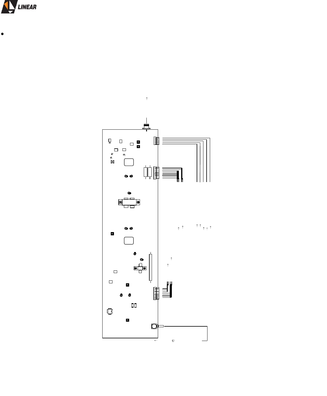
CIP8209 card
Fig. 5.3: 25W Amplifier – DC & RF connections diagram
(OR) +32V RES PIN 1 –CON14 –POWER SUPPLY
(WH) GND PIN 1 –CON9 –POWER SUPPLY
(OR) +32V RES PIN 1 –CON14 –POWER SUPPLY
(WH) GND PIN 1 –CON9 –POWER SUPPLY
(WH) GND PIN 1 –CON9 –POWER SUPPLY
(BL) +18V PIN 1 –CON13 –POWER SUPPLY
(YL) FOWARD POWER READING PIN 4 –CON9 –CONTROL UNIT
(GR) TEMPERATURE ALARM PINO 7 –CON-6 –CONTROL UNIT
TPO-1
T1 ID ADJUST CURRENT:
1,5V in R9 // R10 with or without RF signal input
TPO-2
T2 ID ADJUST CURRENT:
5V in R17 // R75 with or without RF signal input
TPO-3
T2 ID ADJUST CURRENT:
37,5mV in R28 // R29 without RF signal input
TPO-4
ADJ READING OF REFLECTED POWER
TPO-5
ADJ READING OF DIRECT POWER
T2
C32
R28
TPO-4
REF
ADJ TPO-5
FWD
ADJ
CON-1 CON-2
CON-3
CON-4
RF OUT
CON-5
T4
R17
.
1
45
8
CI-3
.
1
4 5
8
.
1
45
8
CI-4
CI-6
.
1
45
8
CI-5
S1
LED 2
LED 1
R29
FW
REF
+15V
TEMP
+30V
C33
H1
C42 C43
T3
C54
C68
C67
H2
TPO-3
T3 VGS
ADJ
TPO-2
T2 VGS
ADJ
C17
C15
.
1
4
5
8
CI-7
.
1
4
5
8
CI-8 D3
D2
TPO-1
T1 VGS
ADJ
T1
R9
R10
123 45678
123 45678
(CABLE BELDEN 50 ) RF INPUT CON-4 –UPCONVERTER UHF
RF OUTPUT CON N FEMALE –RF OUT –REAR PANEL
123 4 5
(GY) REFLECTED POWER READING PIN 2 –CON9 –CONTROL UNIT

AT725P Owner’s Manual
© 2009 Linear Industries, Inc. All Rights Reserved AT725P_OM_08/09 36/75
CIP8209 card – adjustment procedures
Connect a coaxial load 50Ω/100W (minimum) at RF output having a good frequency response (470MHz
860MHz).
Adjusting bias ID of T1, T2 and T3
For T1:
TPO-1 makes the adjustment of the chain of drain (ID) of T1. This adjustment is made measuring the drop of
tension in the resistive parallel set formed by R9 and R10 (2 x 10Ω /1W), being the adjusted one for 1.5V,
what it corresponds 300Ma of ID. This is a class A polarization adjustment.
For T2:
TPO-2 adjusts the voltage VGS of the T2 and, consequently, the bias drain (ID). This adjustment is made
measuring the voltage drop in the resistive parallel set R17 and R75 (2 x 10Ω)/10W), being adjusted for 5V,
what it corresponds to a bias current of drain ID equal 1.0A. This is a class A polarization adjustment.
For T3:
TPO-3 adjusts the voltage VGS of transistor T3 and, consequently, the chain of drain (ID). This adjustment is
made measuring the voltage drop in the resistive parallel set R28 and R29 (2 x 0.12Ω)/10W), being adjusted
for 3.7Mv, what it corresponds to a bias current of drain ID equal 600Ma, or 300Ma for each branch of T3.
This is a class AB polarization adjustment.
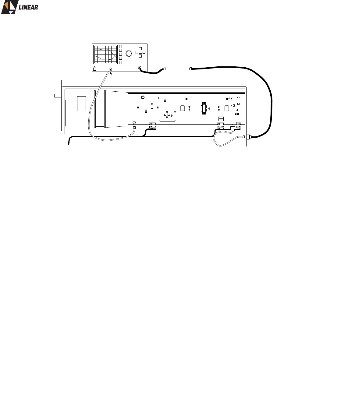
CIP8209 card – frequency response adjustment
Module 4408 is a UHF broadband amplifier that must have its frequency response optimized for higher gain
focused on the operational transmission channel. The factory adjustments must stay even when a LDMOS
transistor replacement becomes is necessary.
The capacitors trimmers present at the module 4408 are the tuning elements to be set for higher possible
gain, at the same time achieving flatness response at the desired UHF operational channel. Below we see
one possible set up suitable for the adjustment of frequency response.
AT725P Owner’s Manual
© 2009 Linear Industries, Inc. All Rights Reserved AT725P_OM_08/09 37/75
T2
C32
R28
TPO-4
REF
ADJ TPO-5
FWD
ADJ
12345678
12345678
12345
CON-1 CON-2
CON-3
CON-4
RF OUT
CON-5
T4
R17
.
1
45
8
CI-3
.
1
45
8
.
1
45
8
CI-4
CI-6
MODULE 4408
20W ATSC TRANSMITTER –AT720P
RF OUTPUT
.
1
45
8
CI-5
S1
LED 2
LED 1
R29
FW
REF
+15V
TEMP
+30V
C33
H1
C42 C43
T3
C54
C68
C67
H2
TPO-3
T3 VGS ADJ
TPO-2
T2 VGS ADJ
C17
C15
.
1
4
5
8
CI-7
.
1
4
5
8
CI-8 D3
D2
TPO-1
T1 VGS ADJ
T1
R9
R10
RFIN
RFOUT
NETWORK ANALYZER
30dB / 100W
ATTENUATOR
-20dBm
Fig.5.3: Frequency Response Adjustment Factory Set Up
Set the network analyzer output level at -20dBm, and connect it at the module 4408 RF input. Tune the
capacitor trimmer for the most flat frequency response over the operational channel. The overall gain should
be 44dB ± 2dB. Remember the bands which the amplifier was designed for:
• LOW BAND (LB): channels 14 to 44
• HIGH BAND (MB): channels 45 to 59

AT725P Owner’s Manual
© 2009 Linear Industries, Inc. All Rights Reserved AT725P_OM_08/09 38/75
Section 6 – Power Supply
Module 4401
General Functional Description
The Power supply - Module 4401 - is of the switching type configured in the topology half bridge, having
overall efficiency above 80%. The module 4401 is responsible for the generation and distribution of following
voltage DC:
• +32V FIXED
• +32V RE-CONNECTABLE
• +18V
• -18V
• +9V
The module 4401 can be connected to the electric AC network of 120Vac or 240Vac, according with internal
jump positions.
The module 4401 is self-protected against DC short-circuit. The protection acts inhibiting the generation of
the switching pulses, shutting down the power supply; 0 volts at the DC’s outputs. The output +32V RE-
CONNECTABLE is commanded by the Control unit.
The re-connection command is sent to the power supply, to turn the +32V RE-CONNECTABLE on.
This voltage is responsible for the feeding of the 25W amplifier - module 4408. The consumption in Amps out
from the +32V RE-CONNECTABLE is basically the consumption associated with the drain electrical current
of the LDMOS transistors of the amplifier. Because of this configuration, the LDMOS currents are measured
at the power supply module 4401.
These currents measurements are routed to the control unit. In case of extremes measured values the
control unit inhibits the +32 RE-CONNECTABLE. Power supply.
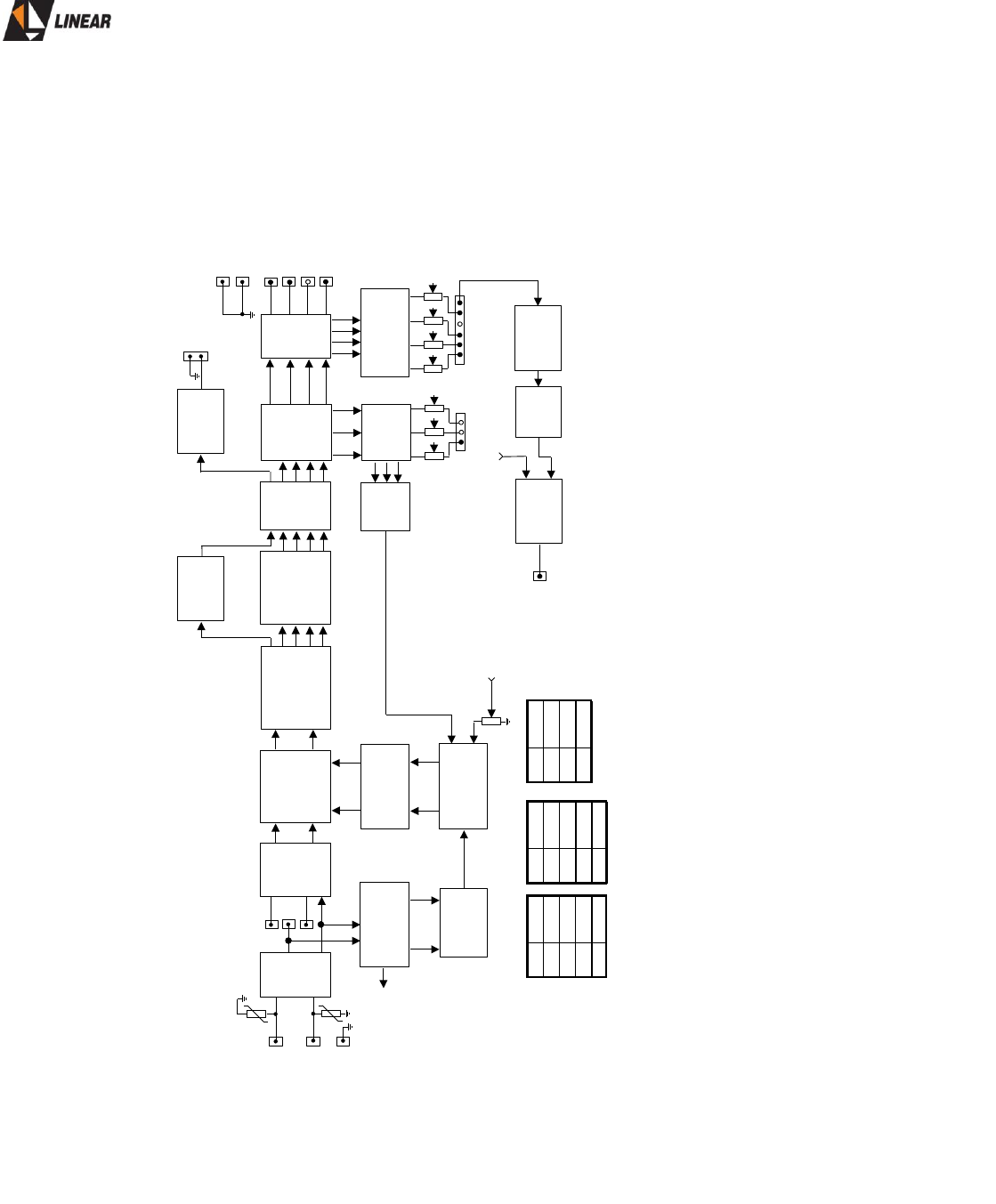
Module 4401 – Block Diagram
Input AC filter
The C1, C6 and TF-1 components together assemble the line filter. This filter minimizes the noise generated
by the power supply into the AC network.

AT725P Owner’s Manual
© 2009 Linear Industries, Inc. All Rights Reserved AT725P_OM_08/09 39/75
The varistors V1, V2 and V3 prevent over-voltage damages potentially caused by occurrences on the AC
network.
The group of diodes D1/D4 rectifies the AC voltage from the AC network and delivers this rectified voltage to
the capacitors C9 and C10 for filtering.
These capacitors could be connected in parallel or in series, according with the set of the jumps for
120/240Vac.
The resistances R1 and R2 are the loads for the capacitors C9 and C10 at the time that the power supply is
powered ON. R3 and R4 provoke a fast discharge of C9 and C10 when the power supply is OFF.
The control of the switching function over the PWM modulator is performed by the components TF-3, D5, D6,
D7, R9, T3, C20, C18 and C46.
Switch and Power
The switching function over the DC input voltage is performed by the Mosfets, T1 and T2. The trigger pulses
are generated by control integrated circuit CI-1, through the transformer TF-4 that also isolates the
modulation circuit from the AC network.
The switching voltage in the transistors is applied in the transformer TF-5 that through the convenient turn’s
ratio, it will generate the voltages in its secondary.
The capacitors C15 and C16 divide the entrance voltage, reducing the voltage over the transistors. C14
prevents the direct-current flow towards TF-5.
The “Snubbers” formed by R7, C17, R34, C31, R37, C35, R43 and C42, help to reduce high frequency noise
generated by the fast and short time switching pulses present on the mosfet transistors as in TF-4.
Rectification and Filtering
The pulses delivered by the several switching and power devices, will be than rectified by D8 to the D14 and
filtered by C32 the C47.
The inductor L2 in its multiple sections, stores the transfer energy that help to filter the signal.
The resistors at the output act as bleeders avoiding undesirables’ transients and oscillations.
Pulse Width Modulation
This block is composed basically by the integrated circuit CI-1 that performs the PWM switching process
control.
CI-1 output (pins 11 and 14) supply the switching pulses that are applied to the transformer TF-4. The “Soft-
Start" system prevents a fast rise of the exit voltage. In this circuit, this function is carried through by C23.

AT725P Owner’s Manual
© 2009 Linear Industries, Inc. All Rights Reserved AT725P_OM_08/09 40/75
Feedback
The resistors R10, R13, R12 and TPO-1 form a voltage divider that take a sample of +32V output of the
power supply and delivery to the comparator CI-1, compares that it with its reference of +5V via R39.
As the value of this sample, the modulation circuit will create a variation in the width of the switching pulses,
having compensating voltage variations in the output voltages.
Protection and Readings
The set of protection acts in case of over-current in the outputs.
In the event of over-current, in any one of the outputs, the voltage in the inverting input of comparators CI-3
and CI-4, transferred by the electrical current readings, will be greater that the voltage of reference in the not
inverting entrance.
This event take the output of the comparator to a low level will trigger a timer formed by CI-2, R26 and C28
that will a voltage at pin 10 of the CI-1 inhibiting the switching process. The electrical current readings are
detected over the power resistors (R44, R45, R36, R40, and R38) and amplified by op-amps getting deep of
scale (4V) proportional the nominal current of each output. All the electrical current readings possess its
proper adjustment:
- TPO-2: +32V/10A
- TPO-3: +18V/1A
- TPO-4: +9V/1A
The readings of output voltage are constituted by operational amplifiers (CI-8, CI-9, CI-10) and each one with
a TPO for full scale adjustment (4V) proportional to the nominal the output voltage.
- TPO-5: +32V
- TPO-6: +32V RECONNECTED.
- TPO-7: -18V
- TPO-8: +18V
- TPO-9: +9V
* NOTES:
1) The current reading is only for the exit of +32V.
2) It does not have reading for the voltage of +32V RECONNECTED.
Reconnection Process
The output of +32V RECONNECTED power supply of the Module 4401 is used to exclusively feed the UHF
amplifier - Module 4408.
AT725P Owner’s Manual
© 2009 Linear Industries, Inc. All Rights Reserved AT725P_OM_08/09 41/75
The +32V RECONNECTED output is a derivation of the +32V FIXED output. This exit is enabled or disabled
by control unit - CIP8231 card board - through the reconnect command. In normal conditions this command
sends +5V to pin 6 of connector CON-8 of CIM3388 (CIP8111) card board of module 4401. Having this
voltage, the switch transistor will be saturated and, consequently, the exit of +32V RECONNECTED will be
enabled.
Fig.6.1: Module 4401 Block Diagram
LF353JCI-5
LM393CI-4
LM393CI-3
LM555CI-2
SG3525CI-1
LM358JCI-10
LM358JCI-9
LM358JCI-8
LM353DCI-7
4N28CI-6
IRFP150T4
TIP29CT3
IRFP450T2
IRFP450T1
TRANSFORMER
12V FOR FAN
LINE
FILTER NETWORK
RETIFIER SWITCHING
TRANSISTORS
SWITCHING
RETIFIER INDUCTOR
FILTER
SWITCHING
RETIFIER
PROTECTION
CIRCUIT
ISOLATOR
TRANSFORMER
CONTROL
NETWORK
TRANSFORMER
CONTROL
SUPPLY
(TF-1) (D1-D4) (T1;T2) (TF-5) (D8; D9)
(D10; D11; D12)
(D13;D14)
(L2-A; L2-B)
(L2-C; L2-D;
L2-F)
(C47)
(CI-1)
(TF-4)
(TF-3)
(D5-D7; T3)
(CI-2)
(CI-3) (CI-4)
CURRENT
DETECTION
+32V RESTARTED
+32V
CON-6
1
2GND
TPO-1
ADJUSTMENT +32V
(R35; R36;R44)
(R38)
CON-4 110V
CON-5
CON-3
220V
110/220VAC
CON-1
CON-2
GND
+32V
+18V
+9V
CURRENT
READING
(CI-5; CI-7)
CON-7
123
TPO-3 TPO-4
TPO-9
ADJUSTMENT READING +9V
TPO-8
ADJUSTMENT READING +18V
TPO-7
ADJUSTMENT READING -18V
TPO-5
ADJUSTMENT READING +32V
+9V
+18V
-18V
+32V
FILTER
VOLTAGE
READING
(CI-8; CI-9; CI-10)
SWITCH
TRANSISTOR
(T4)
CON-8
1 2 34 5
RES
6
NC
ISOLATOR
(CI-6) (CI-4A)
CON-12
CON-13
CON-14
+18V
-18V
COMPARATOR
CON-11 +9V
(C32; C33)
(C36; C37)
(C39; C40)
(C43; C44)
TPO-8
TPO-9 TPO-7 TPO-5
+32V
CON-9
CON-10 +GND
+GND
CON-15 +32V
NETWORK
READING
AT725P Owner’s Manual
© 2009 Linear Industries, Inc. All Rights Reserved AT725P_OM_08/09 42/75
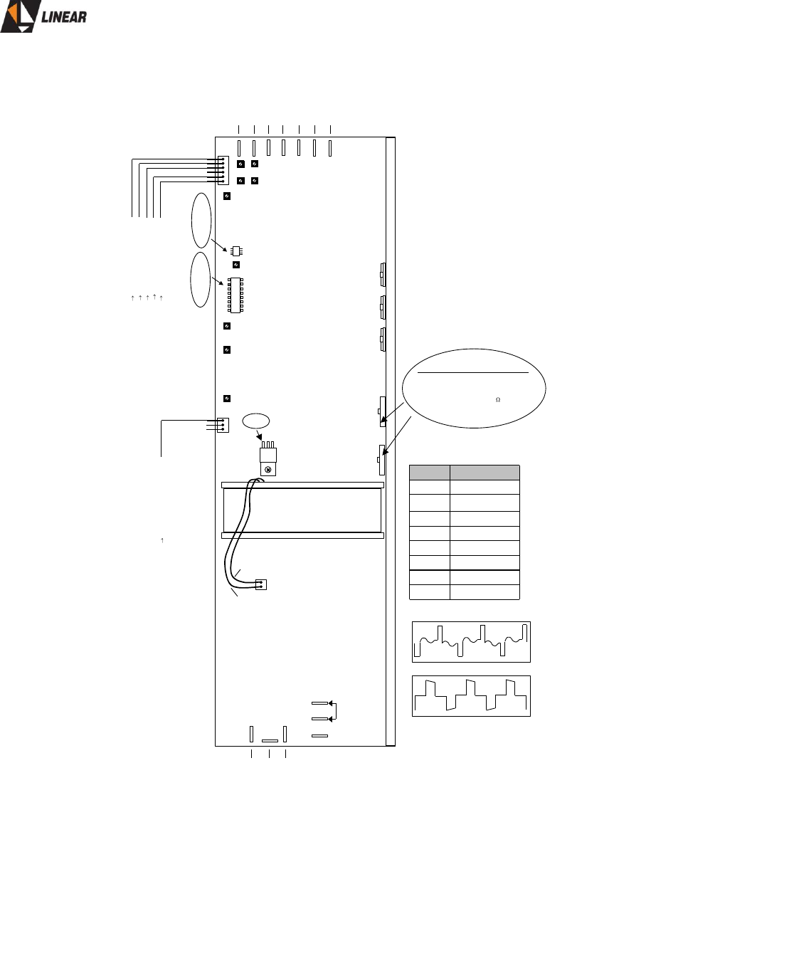
Fig.6.2: Module 4401 – Main components board displacement
1A
2A
3A
1B
2B
3B
4B
5B
6B
(GY) RESTART PIN 6 –CON-3 –CONTROL UNIT
(RD) +32V READING PIN 9 –CON-9–CONTROL UNIT
(OR) CURRENT READING (+32V) PIN 8 –CON-9 –CONTROL UNIT
CON9
CON10
CON11
CON12
CON13
CON14
CON15
WH) GND
(WH) GND
(GR) +9V
(BL) +18V
(OR) +32V REL
(RD) +32V
CON1
GND
CON2
(BR) AC
(WH) GND
(BK) AC
1
2
CON6
CON7 CON8
CON5
110V
CON4
0V
CON3
220V
(BK) GND FAN
(RD) +12V FAN
TPO-2 TPO-4 TPO-3
TPO-1
TPO-6
TPO-5
TPO-7
TPO-8 TPO-9
(BK) -18V *
CI-1
SG3525
.
10
SDG
T1
SDGT2 D8 D12 D9
VENT.
T3
~ +14V
.
CI-2
0V: normal
1,5V: inhibited switching 0V: normal
5V: inhibited switching
3
TEST OF THE INTERNAL DIODES OF T1 AND T2
SWITCH OFF the power!
Digital Multimeter in the scale of diode test.
Test made with T1 and T2 soldiers in the board
Tip (+) in S and tip (-) in D: ~500
Tip (-) in S and tip (+) in D: infinite resistance
CI-1 SG3525
Switching Pulse11, 14
Shut Down 10
Oscillator5
+4,5V (soft-start)8
Ground (GND)12
+15V (supply)13,15
+5V
2
PINS
16 +5V (reference voltage)
CI-1 pin 14 –OUTPUT +32V WITH LOAD
CI-1 pin 14 –OUTPUT +32V WITHOUT LOAD
TPO-1
Adjustment output voltage +32V
TPO-2
Adjustment reading output current +32V
TPO-3
** Adjustment reading output current +18V
TPO-4
** Adjustment reading output current +9V
TPO-5
Adjustment reading output voltage +32v
TPO-6
** Adjustment reading output voltage +32V RESTART
TPO-7
Adjustment reading output voltage -18V
TPO-8
Adjustment reading output voltage +18V
TPO-9
Adjustment reading output voltage +9V
FUNCTION (MEASURE)
(BK) –18V READING PIN 6 –CON-9 –CONTROL UNIT
(GR) +8V READING PIN 5 –CON-9 –CONTROL UNIT
(BL) +18V READING PIN 7 –CON-9 –CONTROL UNIT

AT725P Owner’s Manual
© 2009 Linear Industries, Inc. All Rights Reserved AT725P_OM_08/09 43/75
MODULE 4401 – Technical Specifications
FEATURE
SPECIFICATION
INPUT AC VOLTAGE
90 TO 140VAC / 180 TO 250VAC
SWITCHING FREQUENCY
50kHz
LINE REGULATION
BETTER THAN 2% FOR ALL
OUTPUTS
OUTPUTS NOMINAL VOLTAGES
AND CURRENTS
+32V / 10A
+18V / 1A
-18V / 1A
+9V / 1A
RIPPLE
300mV (+32V)
120mV (+18V / +9V)
80mV (-18V)
LOAD REGULATION
BETTER THAN 2% FOR +32V
BETTER THAN 25% FOR +18V,
-18V, +9V
EFFICIENCY
BETTER THAN 80%
OUTPUT OVER CURRENT LIMIT
30% UPPER NOMINAL VALUE
RESTART VOLTAGE
HIGH LEVEL: > 3.5 TO 5Vdc
LOW LEVEL: < 3.3Vdc
SHUTDOWN VOLTAGE
HIGH LEVEL: > 0.7 TO 5Vdc
LOW LEVEL: < 0.7Vdc
POWER SUPPLY
CIRCUIT
CIM
CIP
POWER
3388A
8111A
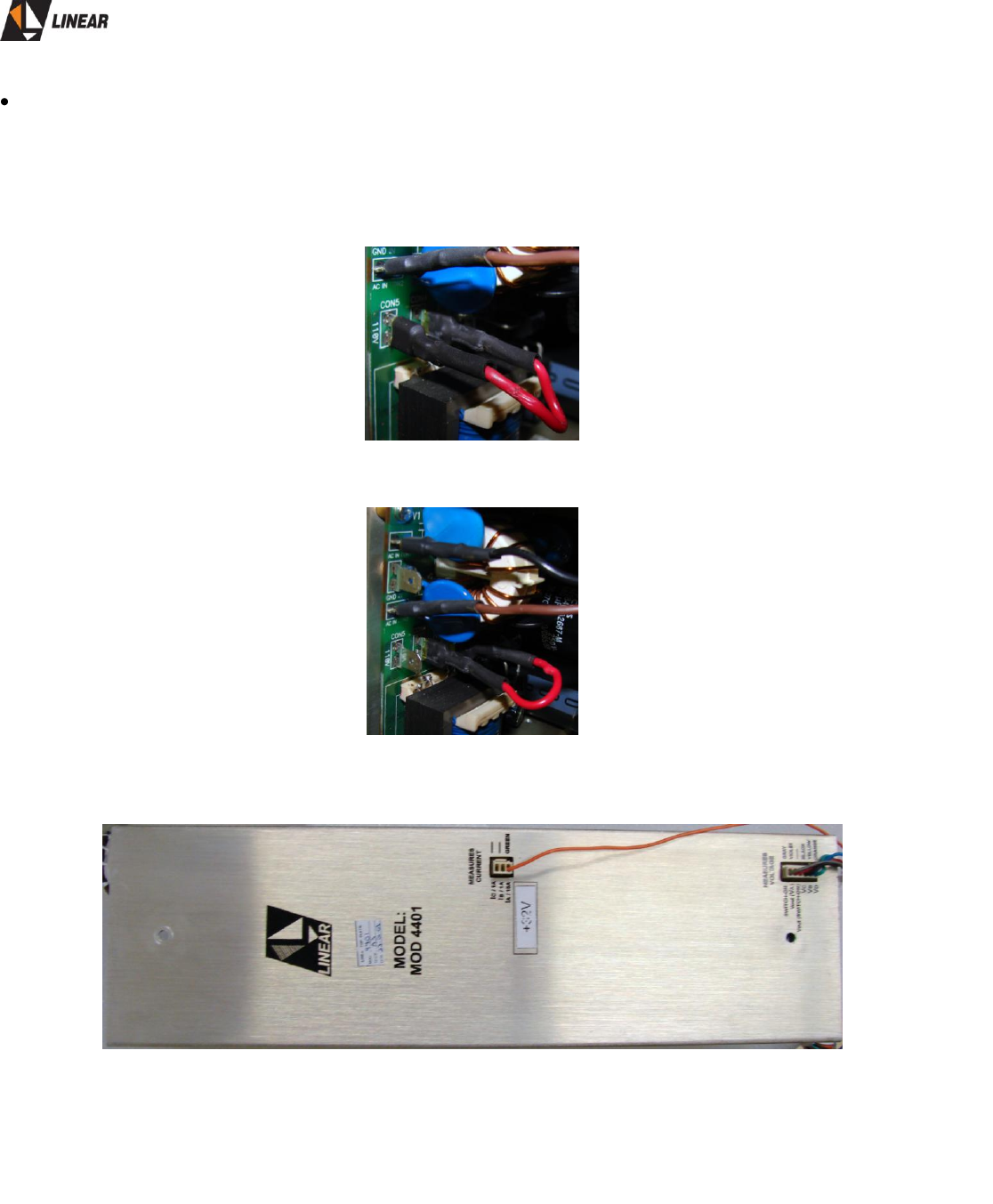
AT725P Owner’s Manual
© 2009 Linear Industries, Inc. All Rights Reserved AT725P_OM_08/09 44/75
MODULE 4401 – Changing the Mains Voltage Operation
The module 4401, on its rear side, is built in such way that it is possible access the 110/220Vac switching
voltage jump. The figures below illustrate the position for the jump for each desired operational voltage. This
is the only required maneuver to change the voltage operation on the AT725P unit.
Fig.6.3: Jump connection for 110Vac operation, (CON5-CON4)
Fig.6.4: Jump connection for 110Vac operation, (CON4-CON3)
Fig.6.5: Module 4401 - +32V Switching Power Supply
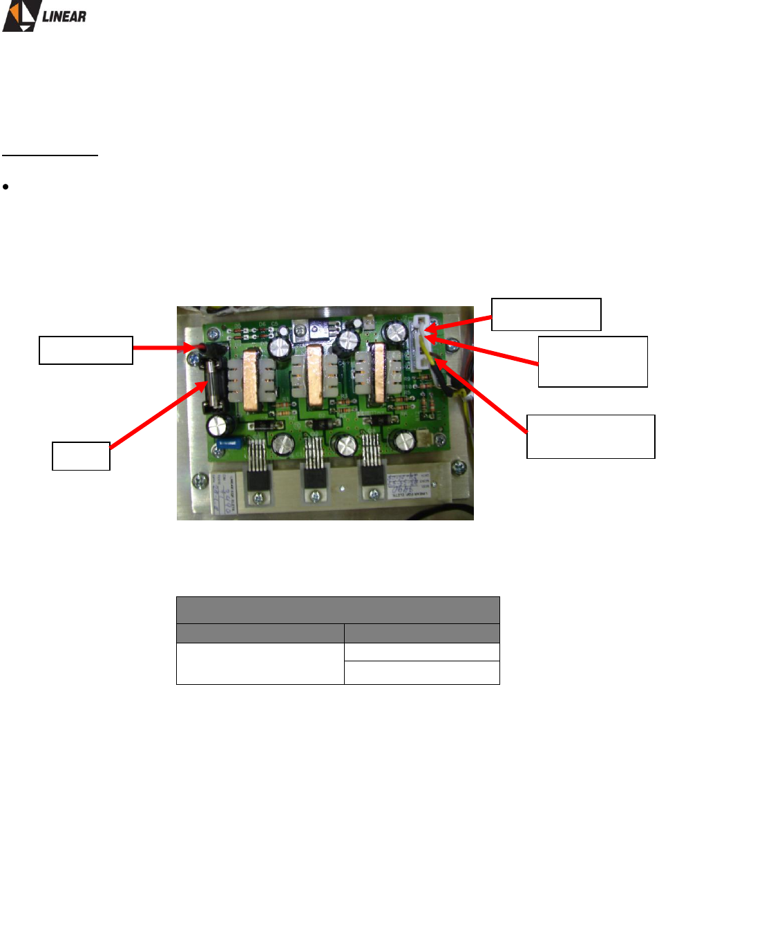
AT725P Owner’s Manual
© 2009 Linear Industries, Inc. All Rights Reserved AT725P_OM_08/09 45/75
Section 7 – DC/DC Converter
Module 4567
General Functional Description
This module has as function to generate specific voltages not present at the main power supply -
module 4401. The module 4567 generates +2.5V and +5V, via standard IC regulators, see below:
Fig.7.1: DC/DC Converter Board
CIM3490 (CIP8390)
INPUT
OUTPUT
+18V
+2.5V (CON-2/2)
+5.0V (CON-2/3)
Fuse
+2.5V Output
Brown wire
+5V Output
Yellow wire
+18V Input
GND wire
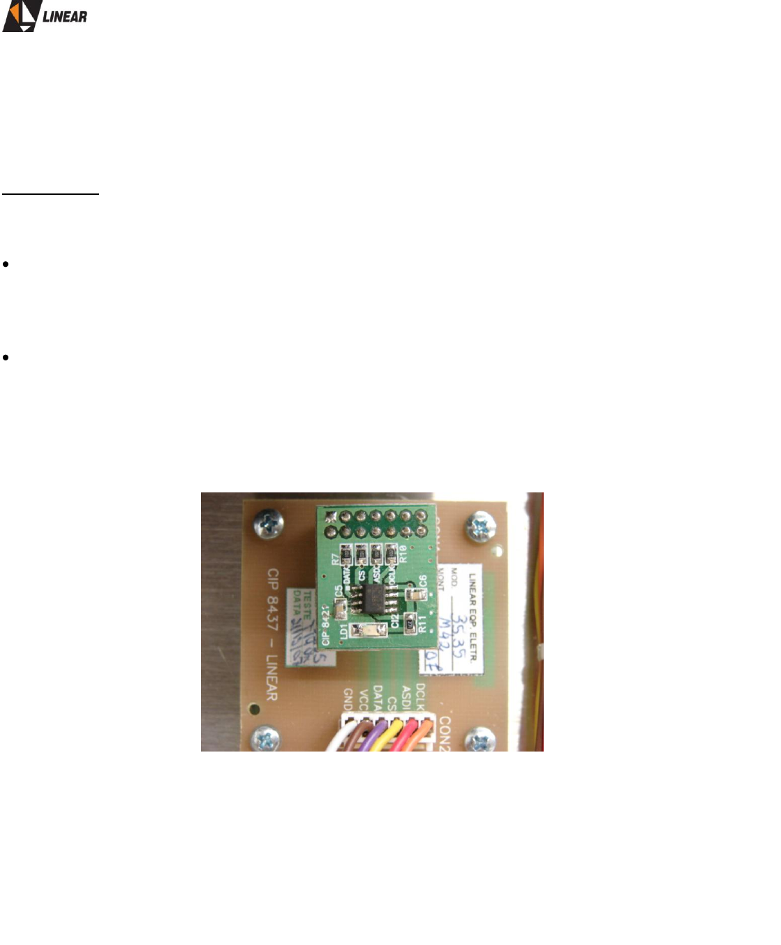
AT725P Owner’s Manual
© 2009 Linear Industries, Inc. All Rights Reserved AT725P_OM_08/09 46/75
Section 8 – Memory Interface
Module 3535
General Functional Description
The connectors CON-4 and CON-10 at the modulator – module CIM3510 – are the communication
connectors with the memory interface CIM3535 mother printed circuit board.
Module CIM3516 – General Functional Description
The 1Mbit LUT memory card – module CIM3516 - is connected to the memory interface - module
3535. This module holds all the non-volatile parameters data related with the digital linear and non-
linear pre-correction.
Fig.8.1: LUT Memory card & module 3535
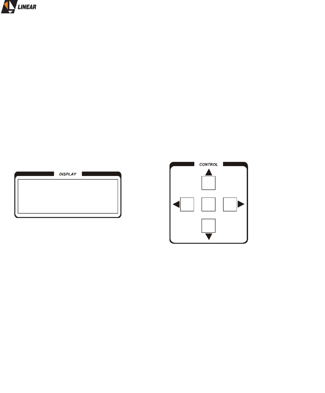
AT725P Owner’s Manual
© 2009 Linear Industries, Inc. All Rights Reserved AT725P_OM_08/09 47/75
Annex A – AT725P Operational Software
AT1012_ASM version 1.2
1. Introduction
The LINEAR family of ADVANCED TV transmitter/Exciter equipment possesses a system for
measurement (measures), configuration (SETUP) and alarms (alarms) all controlled by a microprocessor
controlled system. This document will demonstrate the navigation, operation and configuration of these
functions.
2. Navigation and Signals
2.1 Keypad and Display
2.1.1 Keypad
Moves the cursor up
Moves the cursor right
Moves the cursor left
Moves the cursor down
Yellow Key “ENTER”

AT725P Owner’s Manual
© 2009 Linear Industries, Inc. All Rights Reserved AT725P_OM_08/09 48/75
2.2 Display
The display navigation is made by the following:
The cursor must be located on the first character of each function to access that function.
It is then activated by pressing the yellow “ENTER” key
During the navigation there will appear in the display special functions that assist navigation, these are:
ESC – Used to return to the previous menu
NXT – Used to access the next screen
CLEAR – Used to clear old alarms
2.3 Signals
During the navigation there will appear in the display signal characters these are:
* – Indicates the presence of a current alarm
# – Indicates the presence of an old alarm
(LOCK) – Indicates that the equipment is configured with password, and that to have access to
that part of the menu the password must be entered.
– The UP and DOWN arrows assist in the movement between screens. When they appear the
UP or DOWN key must be used to move between screens. If in a measurement screen, to return to the
previous menu, any key can be pressed.
MEASURES SETUP
NXT ESC
MEASURES SETUP
NXT ESC
MEASURES SETUP
NXT ESC
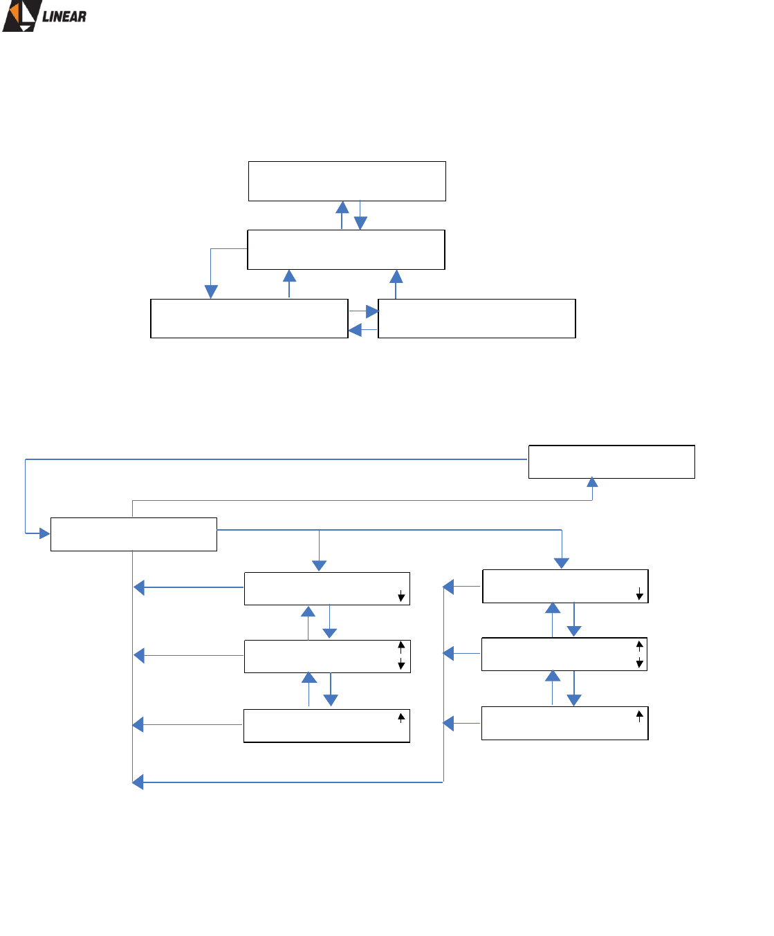
AT725P Owner’s Manual
© 2009 Linear Industries, Inc. All Rights Reserved AT725P_OM_08/09 49/75
3. Screen Flow Charts
3.1 Main screens
Main screens
3.2 Measurement Screen 1
LINEAR INDUSTRIES
INC.
AT720P
MEASURES SETUP
NXT ESC
ALARMS REMOTE
NXT ESC
[Esc] [Esc]
[Any Key]
LINEAR INDUSTRIES
INC.
LINEAR INDUSTRIES
INC.
AT720P
MEASURES SETUP
NXT ESC
MEASURES SETUP
NXT ESC
MEASURES SETUP
NXT ESC
ALARMS REMOTE
NXT ESC
ALARMS REMOTE
NXT ESC
ALARMS REMOTE
NXT ESC
[Esc] [Esc]
[Any Key]
MEASURES SETUP
NXT ESC
POWER P.SUPPLY
NXT ESC
FWD. PWR.: W
RFL. PWR.: W
ALC STATUS:
ALC R.V: V
P.A. TEMPERATURE:
+32V: + V
+18V: + V
+ 9V: + V
-18V: - V
I1: A
[Measures ]
[Esc]
[Power ] [P.Supply ]
[Up and Down Keys ]
[Enter Key ]
MEASURES SETUP
NXT ESC
MEASURES SETUP
NXT ESC
MEASURES SETUP
NXT ESC
POWER P.SUPPLY
NXT ESC
POWER P.SUPPLY
NXT ESC
FWD. PWR.: W
RFL. PWR.: W
FWD. PWR.: W
RFL. PWR.: W
ALC STATUS:
ALC R.V: V
ALC STATUS:
ALC R.V: V
P.A. TEMPERATURE:P.A. TEMPERATURE:
+32V: + V
+18V: + V
+32V: + V
+18V: + V+18V: + V
+ 9V: + V
-18V: - V
+ 9V: + V
-18V: - V
I1: AI1: A
[Measures ]
[Esc]
[Power ] [P.Supply ]
[Up and Down Keys ]
[Enter Key ]
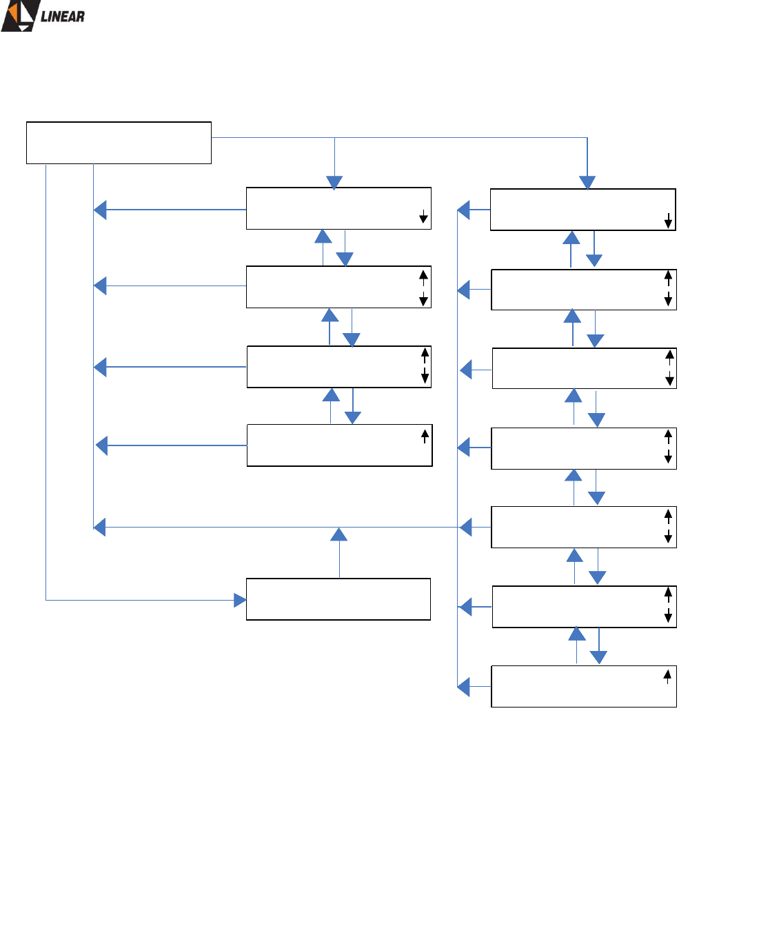
AT725P Owner’s Manual
© 2009 Linear Industries, Inc. All Rights Reserved AT725P_OM_08/09 50/75
3.3 Measurement Screen 2
TR.STR. STATUS
NXT SOFTWARE ESC
DATA PACKETS RATE:
Mbps
NULL PACKETS RATE:
Mbps
FIFO OCCUPATION:
%
TRANSPORT STREAM:
SOFTWARE:
VERSION:
PASSWORD ON:
PILOT LEVEL:
CHANNEL:
LO N.I: mV
LO N.Q: mV
TX.BAL.I:
PHASE I:
TX.BAL.Q:
PHASE Q:
DPD SCALE :
DPD ACTIVE:
[Status ][Tr.Stream ]
[Up and Down keys ]
[Enter Key]
[Software ]
TR.STR. STATUS
NXT SOFTWARE ESC
TR.STR. STATUS
NXT SOFTWARE ESC
DATA PACKETS RATE:
Mbps
DATA PACKETS RATE:
Mbps
NULL PACKETS RATE:
Mbps
NULL PACKETS RATE:
Mbps
FIFO OCCUPATION:
%
FIFO OCCUPATION:
%
TRANSPORT STREAM:TRANSPORT STREAM:
SOFTWARE:
VERSION:
SOFTWARE:
VERSION:
PASSWORD ON:PASSWORD ON:
PILOT LEVEL:PILOT LEVEL:
CHANNEL:CHANNEL:
LO N.I: mV
LO N.Q: mV
LO N.I: mV
LO N.Q: mV
TX.BAL.I:
PHASE I:
TX.BAL.I:
PHASE I:
TX.BAL.Q:
PHASE Q:
TX.BAL.Q:
PHASE Q:
DPD SCALE :
DPD ACTIVE:
DPD SCALE :
DPD ACTIVE:
[Status ][Tr.Stream ]
[Up and Down keys ]
[Enter Key]
[Software ]
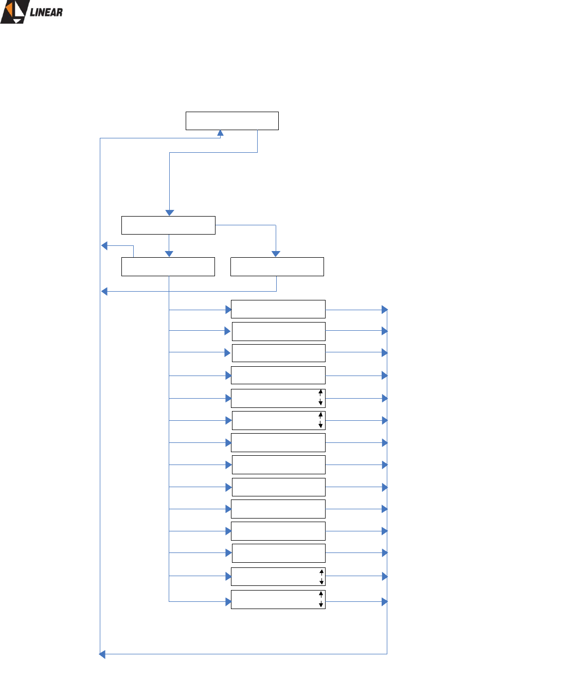
AT725P Owner’s Manual
© 2009 Linear Industries, Inc. All Rights Reserved AT725P_OM_08/09 51/75
3.4 Configuration Screen
[Enter Key]
MEASURES SETUP
NXT ESC
TYPE PASSWORD:
NXT YES PREV ESC
WRONG PASSWORD !
TYPE PASSWORD:
ENABLE PASSWORD:
YES NO
TYPE PILOT LEVEL:
TYPE CHANNEL:
FACTORY SETUP
TYPE LO NULL I:
TYPE LO NULL Q:
TYPE AMPLITUDE I:
TYPE PHASE I:
TYPE AMPLITUDE Q:
TYPE PHASE Q:
TYPE DPD SCALE:
DPD ACTIVE:
YES NO
ALC. R.V.: [V]
POWER : [W]
TYPE CONFIG.:
[Yes]
[Enter Key ]
[Wrong Password and Enter Key ]
[Correct Password
and Enter Key ]
[Esc]
[Enter Key]
MEASURES SETUP
NXT ESC
MEASURES SETUP
NXT ESC
MEASURES SETUP
NXT ESC
TYPE PASSWORD:TYPE PASSWORD:
NXT YES PREV ESCNXT YES PREV ESC
WRONG PASSWORD !WRONG PASSWORD !
TYPE PASSWORD:TYPE PASSWORD:
ENABLE PASSWORD:
YES NO
ENABLE PASSWORD:
YES NO
TYPE PILOT LEVEL:TYPE PILOT LEVEL:
TYPE CHANNEL:
FACTORY SETUP
TYPE CHANNEL:
FACTORY SETUP
TYPE LO NULL I:TYPE LO NULL I:
TYPE LO NULL Q:TYPE LO NULL Q:
TYPE AMPLITUDE I:TYPE AMPLITUDE I:
TYPE PHASE I:TYPE PHASE I:
TYPE AMPLITUDE Q:TYPE AMPLITUDE Q:
TYPE PHASE Q:TYPE PHASE Q:
TYPE DPD SCALE:TYPE DPD SCALE:
DPD ACTIVE:
YES NO
DPD ACTIVE:DPD ACTIVE:
YES NO
ALC. R.V.: [V]
POWER : [W]
ALC. R.V.: [V]
POWER : [W]
TYPE CONFIG.:TYPE CONFIG.:
[Yes]
[Enter Key ]
[Wrong Password and Enter Key ]
[Correct Password
and Enter Key ]
[Esc]
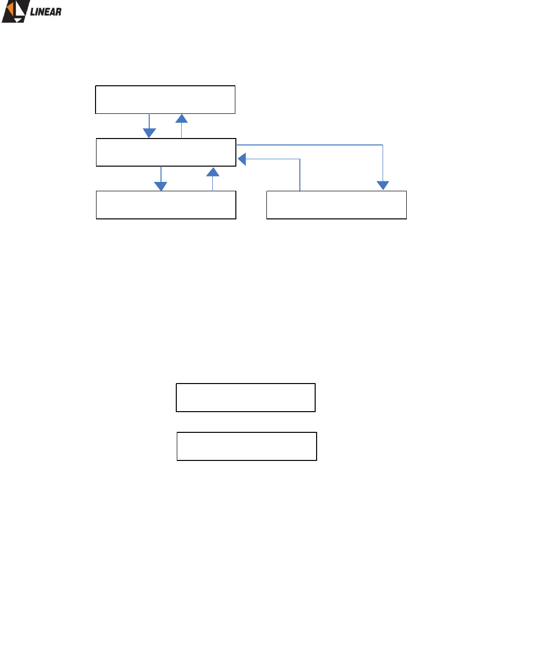
AT725P Owner’s Manual
© 2009 Linear Industries, Inc. All Rights Reserved AT725P_OM_08/09 52/75
3.5 Alarm Screen
4. Initialization
When the equipment is initially switched on the screen backlight lights automatically and the message
“LOADING”… is displayed, indicating the load process of the modulator has begun. In the unlikely case that
the equipment continues showing this message, the possibility of software error has occurred in the load
process of the modulator and the equipment may not enter into correct operation. Please report this status to
Linear Industries Inc for the necessary steps of action. Following the LOADING message, the name of the
manufacturer, the type number of the equipment, normal rated RMS power and the operating channel are
displayed.
This information alternates approximately every 2 seconds. The backlight switches off after approximately 20
seconds. After this initialization of the equipment these indications will remain indefinitely until another key is
pressed. When pressing another key the backlight will light again. Depending on the type of screen the
cursor will automatically locate itself in one of the options. To execute some of these options, after the
backlight has extinguished it may be necessary to press any key again. If no option is chosen, the backlight
will switch off in approximately 20 seconds and then after approximately five minutes the screen returns to
the initial display.
ALARMS REMOTE
NXT ESC
CURRENT PAST
ESC
NXT CLR. ALL ESC
NXT ESC
[Esc]
[Alarms ][Past]
[Esc]
[Current ][Esc]
ALARMS REMOTE
NXT ESC
ALARMS REMOTE
NXT ESC
ALARMS REMOTE
NXT ESC
CURRENT PAST
ESC
CURRENT PAST
ESC
NXT CLR. ALL ESCNXT CLR. ALL ESC
NXT ESC
NXT ESC
NXT ESC
[Esc]
[Alarms ][Past]
[Esc]
[Current ][Esc]
AT720P
20W UHF
AT720P
20W UHF
LINEAR INDUSTRIES
INC.
LINEAR INDUSTRIES
INC.

AT725P Owner’s Manual
© 2009 Linear Industries, Inc. All Rights Reserved AT725P_OM_08/09 53/75
4.1 MEASURE MENU
The measure menu allows access to the general equipment configuration parameters; power levels,
TS feed and status, qualification of passwords, cancellation of the L.O signal., rejection of image frequency
signal, level of scale, activation of look up tables (LUTs) for pre-distortion and the name and version of the
installed software on the central microcontroller.
Navigation through these screens is made with the keys UP and DOWN. When these are displayed it
is not possible to configure any parameters. The “ENTER” key must be pressed to return to the main screen.
4.1.1 POWER MENU
The power menu displays the forward and reflected power at the output of the equipment, measured
at the output power reflectometer. Also displayed are the ALC reference voltage and the temperature of the
final RF output amplifier.
To have access to the POWER screen, the following sequence of screens is necessary:
Access MEASURES
Access POWER
Use the key “DOWN” to see the next set of screens.
POWER P.SUPPLY
NXT ESC
POWER P.SUPPLY
NXT ESC
MEASURES SETUP
NXT ESC
MEASURES SETUP
NXT ESC
MEASURES SETUP
NXT ESC
FWD. PWR.: W
RFL. PWR.: W
ALC STATUS:
ALC R.V: V
P.A. TEMPERATURE:
FWD. PWR.: W
RFL. PWR.: W
FWD. PWR.: W
RFL. PWR.: W
ALC STATUS:
ALC R.V: V
ALC STATUS:
ALC R.V: V
P.A. TEMPERATURE:P.A. TEMPERATURE:

AT725P Owner’s Manual
© 2009 Linear Industries, Inc. All Rights Reserved AT725P_OM_08/09 54/75
To return to the previous screen, press the UP key. To return the POWER option presses “ENTER”. NOTE:
The screens above are a rolling type, allowing access to all of the voltage measurements by using the UP
and DOWN keys.
4.1.2 POWER SUPPLY MENU
This screen displays the voltages and currents of the principal equipment power supplies.
To have access to the P.SUPPLY screen the sequence of screens are:
Access MEASURES
Access P.SUPPLY
Use the key “UP and DOWN” to move between screens.
To return to the previous screen press the key UP. To return to the option P.SUPPLY press “ENTER”.
4.1.3 MENU ESC
Pressing ESC returns the cursor to the previous screen.
4.1.4 MENU NXT
Selecting the “NXT” option provides access to more options of measurement. The sequence for
access of these measurements is shown below:
POWER P.SUPPLY
NXT ESC
POWER P.SUPPLY
NXT ESC
MEASURES SETUP
NXT ESC
MEASURES SETUP
NXT ESC
MEASURES SETUP
NXT ESC
+32V: + V
+18V: + V
+ 9V: + V
-18V: + V
I1: A
+32V: + V
+18V: + V
+32V: + V
+18V: + V+18V: + V
+ 9V: + V
-18V: + V
+ 9V: + V
-18V: + V
I1: AI1: A

AT725P Owner’s Manual
© 2009 Linear Industries, Inc. All Rights Reserved AT725P_OM_08/09 55/75
4.1.5 MENU TR.STR.
TR STR shows information about the input digital signal.
Select NXT and press ENTER
Select TR.STR and press ENTER
To return to the previous screen press the UP key. To return to the TR.STR options press ENTER.
4.1.6 MENU STATUS
4.1.6.1 Password qualification state
This screen shows the information on the configured parameters:
PASSWORD ON: YES - indicates that a password is required to enter into the SETUP MENU, and will be
asked for to each attempt of access this menu.
MEASURES SETUP
NXT ESC
MEASURES SETUP
NXT ESC
MEASURES SETUP
NXT ESC
TR.STR. STATUS
NXT SOFTWARE ESC
TR.STR. STATUS
NXT SOFTWARE ESC
DATA PACKETS RATE:
Mbps
NULL PACKETS RATE:
Mbps
FIFO OCCUPATION:
%
TRANSPORT STREAM:
DATA PACKETS RATE:
Mbps
DATA PACKETS RATE:
Mbps
NULL PACKETS RATE:
Mbps
NULL PACKETS RATE:
Mbps
FIFO OCCUPATION:
%
FIFO OCCUPATION:
%
TRANSPORT STREAM:TRANSPORT STREAM:

AT725P Owner’s Manual
© 2009 Linear Industries, Inc. All Rights Reserved AT725P_OM_08/09 56/75
PASSWORD ON: NO - indicates that the requirement of a password is not necessary to enter into the
SETUP MENU and open access is available.
Below is the sequence necessary for this option:
Select STATUS and press ENTER
4.1.6.2 Amplitude level of the ATSC Pilot carrier:
This is a numerical value relative to the carrier pilot level.
PILOT LEVEL: <+511 TO -2048>
Access to the STATUS menu can be via the far left option or from the PASSWORD ON screen: following
viewing the programmed level press the UP and DOWN keys to navigate to other STATUS screens.
4.1.6.3 Transmission channel
This screen displays the factory programmed transmission channel.
CHANNEL <2 to 59>
To have access to this menu navigate via the STATUS option and then select PILOT LEVEL: pressing the
UP and DOWN key and then the factory programmed channel can be viewed.
TR.STR. STATUS
NXT SOFTWARE ESC
TR.STR. STATUS
NXT SOFTWARE ESC
PASSWORD ON:PASSWORD ON:
PASSWORD ON:
PILOT LEVEL:
PASSWORD ON:PASSWORD ON:
PILOT LEVEL:PILOT LEVEL:

AT725P Owner’s Manual
© 2009 Linear Industries, Inc. All Rights Reserved AT725P_OM_08/09 57/75
4.1.6.4 DC voltage level adjustment for the cancellation of the L.O signal:
This level indicates the voltage programmed in the Up Converter for the cancellation of the local oscillator
signal.
LO N.I.: and LO N.Q. <0.00 to 49.75 mV>:
To have access this menu, select the option STATUS
CHANNEL: press UP and DOWN key
4.1.6.5 Rejection of the frequency image:
The following are numerical values related to the amplitude and phase signal for rejection of the image
frequency.
TX. BAL. Q: - <00000 to 32767>
PHASE Q: - <-32767 to +32767>
TX. BAL. I: - <00000 to 32767>
PHASE I: - <-32767 to +32767>
PILOT LEVEL:
CHANNEL:
PILOT LEVEL:PILOT LEVEL:
CHANNEL:CHANNEL:
CHANNEL:
LO N.I: mV
LO N.Q: mV
CHANNEL:CHANNEL:
LO N.I: mV
LO N.Q: mV
LO N.I: mV
LO N.Q: mV
LO N.I: mV
LO N.Q: mV
TX.BAL.I:
PHASE I:
TX.BAL.Q:
PHASE Q:
LO N.I: mV
LO N.Q: mV
LO N.I: mV
LO N.Q: mV
TX.BAL.I:
PHASE I:
TX.BAL.I:
PHASE I:
TX.BAL.Q:
PHASE Q:
TX.BAL.Q:
PHASE Q:

AT725P Owner’s Manual
© 2009 Linear Industries, Inc. All Rights Reserved AT725P_OM_08/09 58/75
4.1.6.6 Pre-distortion scale level:
This is a scale (or intensity) of the pre-distortion level applied to the transmission signal.
DPD SCALE: < 0000 to 4095>
4.1.6.7 Qualification of pre-distortion tables:
DPD ACTIVE: YES – indicates the signal pre-distortion tables are active
DPD ACTIVE: NO - - indicates the signal pre-distortion tables are not active.
4.1.6.8 Name and version of software:
This menu indicates the name and the version of recorded software in the central microcontroller. This
information must be provided to the factory in the case of any maintenance request.
SOFTWARE: < ATXXXX >
VERSION: < X.X >
TX.BAL.Q:
PHASE Q:
DPD SCALE :
DPD ACTIVE:
TX.BAL.Q:
PHASE Q:
TX.BAL.Q:
PHASE Q:
DPD SCALE :
DPD ACTIVE:
DPD SCALE :
DPD ACTIVE:
TX.BAL.Q:
PHASE Q:
DPD SCALE :
DPD ACTIVE:
TX.BAL.Q:
PHASE Q:
TX.BAL.Q:
PHASE Q:
DPD SCALE :
DPD ACTIVE:
DPD SCALE :
DPD ACTIVE:

AT725P Owner’s Manual
© 2009 Linear Industries, Inc. All Rights Reserved AT725P_OM_08/09 59/75
To verify the name and version of software select the option SOFTWARE after that press ENTER.
Select SOFTWARE and press ENTER
4.2 MENU SETUP
This menu allows access to the configuration functions and parameters of operation of the equipment. The
RIGTH ARROW and LEFT ARROWkeys locate the cursor in each one of the four possible digits and the “+”
and “-” keys and the ENTER and UP and DOWN keys change the digits. The “ENTER” key finalizes the
numerical value to the control system. Without pressing the “ENTER” key the value is not remembered.
Before the “ENTER” key is pressed the parameter is only adjusted in real time for review of the measured
results. If the equipment is switched off during a parameter configuration before pressing the “ENTER” key
the configuration will not be saved in the memory and the same values will be as previously stored.
4.2.1 MENU TYPE PASSWORD
This menu is to set the four numerical password digits to have access to the SETUP functions. This menu is
active only when option YES in the ENABLE PASSWORD menu is indicated. The RIGTH ARROW and
LEFT ARROW keys position the cursor in each one of the four possible digits and the ENTER and UP and
DOWN keys edit the digits. The “ENTER” key transmits the value of the password to the control system.
It is only possible to leave this screen after entering the numerical password.
If the correct password is entered access to the SETUP options is available. If the incorrect password is
entered the following is message is shown “WRONG PASSWORD” and the equipment returns automatically
to the main options menu.
TYPE PASSWORD: <XXXX>
Below is the sequence of access for this menu:
TR.STR. STATUS
NXT SOFTWARE ESC
TR.STR. STATUS
NXT SOFTWARE ESC
SOFTWARE:
VERSION:
SOFTWARE:
VERSION:
MEASURES SETUP
NXT ESC
MEASURES SETUP
NXT ESC
MEASURES SETUP
NXT ESC

AT725P Owner’s Manual
© 2009 Linear Industries, Inc. All Rights Reserved AT725P_OM_08/09 60/75
Select SETUP and press ENTER
Type the password number and then press “ENTER”
4.2.2 LIST OF MENU OPTIONS:
The following allows navigation in the equipment configuration options:
NXT: executes the navigation option
PREV: returns to the previous menu
YES: indicates access to that particular option
ESC: returns to the main options menu
To see the options select NXT and press “ENTER”. When the required option is shown, locate the cursor on
the “YES” and press “ENTER”.
4.2.2.1 < SET NEW PASSWORD? >
This menu allows the four numerical digits to be configured as a new password for the equipment. The
RIGTH ARROW and LEFT ARROW keys locate the cursor on one of the four digits to be changed and the
ENTER and UP and DOWN keys change the digits. Pressing “ENTER” key then informs the new password
to the control system and returns to the main options menu.
It is only possible to leave this screen after entering the numerical password.
4.2.2.2 < ENABLE PASSWORD? >
This option allows the qualification or not of the password programmed in SET NEW PASSWORD option.
TYPE PASSWORD:TYPE PASSWORD:
TYPE PASSWORD:TYPE PASSWORD:
NXT YES PREV ESCNXT YES PREV ESC

AT725P Owner’s Manual
© 2009 Linear Industries, Inc. All Rights Reserved AT725P_OM_08/09 61/75
YES: confirms the requirement of the password to have access to the SETUP options menu.
NO: Indicates that no password is required to have access to the SETUP options menu.
.
4.2.2.3 < SET PILOT LEVEL? >
This option allows the configuration of the desired level of the ATSC signal pilot carrier with the following
band of values: < +511 TO -2048 >.
4.2.2.4 < SET CHANNEL? >
For equipment safety reasons changing channel is not allowed in the on-site configuration. This procedure
can only be configured in the factory. Changing the channel without the permission of a factory trained
engineer can potentially void any warranty on the product.
4.2.2.5 < SET LO NULL I? >
This menu allows the DC voltage adjustment for “nulling” the “I” signal from the local oscillator inter-
modulation in the Up Converter. The adjustment has the following potential values: < 0.00 to 49.75 mV >.
ENABLE PASSWORD:
YES NO
ENABLE PASSWORD:
YES NO
TYPE PILOT LEVEL:TYPE PILOT LEVEL:
TYPE CHANNEL:
FACTORY SETUP
TYPE CHANNEL:
FACTORY SETUP
TYPE LO NULL I:TYPE LO NULL I:

AT725P Owner’s Manual
© 2009 Linear Industries, Inc. All Rights Reserved AT725P_OM_08/09 62/75
4.2.2.6 < SET LO NULL Q? >
This menu allows the DC voltage adjustment for “nulling” the “Q” signal from the local oscillator inter-
modulation in the Up Converter. The adjustment has the following potential values: < 0.00 to 49.75 mV >.
4.2.2.7 < SET TX BAL. AMP. I? >
This menu allows the adjustment of the “I” amplitude of the image rejection signal in the 8VSB modulator
with the following band of values: < 00000 to 32767 >.
4.2.2.8 < SET PHASE I? >
This menu allows the adjustment of the “I” phase of the image rejection signal in the 8VSB modulator with
the following band of values: < 00000 to 32767 >.
4.2.2.9 < SET TX BAL. AMP. Q? >
This menu allows the adjustment of the “I” balance of the image rejection signal in the 8VSB modulator with
the following band of values: < 00000 to 32767 >.
4.2.2.10 < SET PHASE Q? >
This menu allows the adjustment of the “Q” phase signal amplitude of image rejection signal in the 8VSB
modulator with the following band of values: < 00000 to 32767 >.
TYPE LO NULL Q:TYPE LO NULL Q:
TYPE AMPLITUDE I:TYPE AMPLITUDE I:
TYPE PHASE I:TYPE PHASE I:
TYPE AMPLITUDE Q:TYPE AMPLITUDE Q:
TYPE PHASE Q:TYPE PHASE Q:

AT725P Owner’s Manual
© 2009 Linear Industries, Inc. All Rights Reserved AT725P_OM_08/09 63/75
4.2.2.11 < SET DPD SCALE? >
This menu allows the configuration of the DPD (Digital Pre-distortion) scale (or intensity) of digital pre-
distortion applied to ATSC signal, with the following band of values : < 0000 to 4095 >
4.2.2.12 < SET DPD ACTIVE? >
This menu allows the activation or not of the digital pre-distortion tables.
YES: activates the use of the digital pre-distortion look up tables (LUT’s)
NO: deactivates the use of the digital pre-distortion look up tables (LUT’s)
4.2.2.13 < SET POWER? >
This allows the configuration of normal rated power at the output of the equipment. The ENTER and UP and
DOWN key increase and decrease the power level. The RIGTH ARROW and LEFT ARROW keys do not
possess any function in this screen. The “ENTER” key memorizes the desired value.
The value of power displayed on this screen is a value fed directly from the output reflectometer and is the
same value that is provided to the ALC system (Automatic Level Control) circuit. The system allows a certain
flexibility of adjustment by providing at the same time the power level display in order to verify the actual
power level. It is not recommended to adjust for very low values of ALC voltage as this may cause the power
to become unstable.
For higher ALC values (above 1.3V) the power will vary with the variation of the ALC voltage. In case this
simultaneous variation does not occur it is likely that there is a fault in either or both the Up Converter or final
RF amplifier. This type of occurrence should be reported to the Linear Industries Inc.
In this screen the ALC is disabled for precise adjustments of the power level and for full manual
control of power using the ENTER and UP and DOWN keys. In any another environment or screen the ALC
system returns to an enabled mode in order to control the power level.
TYPE DPD SCALE:TYPE DPD SCALE:
DPD ACTIVE:
YES NO
DPD ACTIVE:DPD ACTIVE:
YES NO
ALC. R.V.: [V]
POWER : [W]
ALC. R.V.: [V]
POWER : [W]

AT725P Owner’s Manual
© 2009 Linear Industries, Inc. All Rights Reserved AT725P_OM_08/09 64/75
WARNING: It is important not to set the programmed values of the ALC and consequently the final
RF power level above the nominal value of the equipment: this may caused damage to the internal
modules and may void the warranty on the unit.
4.2.2.14 < SET CONFIGURATION? >
This menu allows the operating mode of the equipment to be configured with regard to including or not an
ATSC compliant mask filter.
Key ENTER: TRANSMITTER
Key UP and DOWN: EXCITER
Configuration TRANSMITTER: in this configuration the transmitter provides approximately 15% more power
than the normal rated power at the reflectometer output. This amount compensates for the losses of the
ATSC compliant mask filter in order that at the output of the filter the correct and nominal rated power level of
the equipment is obtained.
Although this compensation is included for the normal rated power, the system still shows the real power
level for nominal values, for example, if 23.3W is measured at the output, the display will read 25W. For this
configuration the functions in the external connector "External Functions" are disabled.
Configuration EXCITER: in this configuration, the transmitter function as a simple Exciter/Driver and it does
not take into consideration the use of an output filter. In this mode the transmitter does not compensate for
loss of power in the output reflectometer. The nominal output power value can directly measured at the
output of the reflectometer; i.e. if the output power is 25W the display will read 25W. For this configuration
the functions in the external connector "External Functions" are active. By means of this connector it is
possible disconnect the power amplifier and inhibit the transmission signal completely with all the inputs still
connected and a completely active control system.
This can be made with the input of a 5V DC level on pin 3 of the male side of the connector DB-9 (external
functions), in which pin 5 is at ground level. 5V on pin 3 disconnects the amplifier and 0V keeps the amplifier
on. With this function it is possible to externally switch on or off the EXCITER and or TRANSMITTER.
4.3 ALARMS MENU
This transmission equipment possesses a system of alarm indications. These are show by symbols at the
right side of the display screen: * and #. The signal * represents the occurrence of a current alarm. The
signal # represents an old alarm, i.e. an alarm that has already occurred and has been normalized (cleared).
Under normal operating conditions neither of these two symbols will be displayed on the screen.
TYPE CONFIG.:TYPE CONFIG.:

AT725P Owner’s Manual
© 2009 Linear Industries, Inc. All Rights Reserved AT725P_OM_08/09 65/75
When the * is displayed on the screen access should be made to the current alarm screen to verify which
alarm is occurring.
4.3.1) CURRENT MENU
This menu displays the current alarm messages i.e. alarms that indicate are still present and have not yet
been normalized or cleared.
The current alarm messages are updated when entering the CURRENT MENU.
To update the list, you must leave the menu and then return to the ALARMS using the ESC option and then
access the CURRENT menu option again.
Option NXT shows the next alarm message. If there are no alarm messages it will read as follows:
< ALARMS LIST START! >
< ALARMS LIST END! >
Option ESC returns to the previous screen.
The following messages may appear on the current alarms list:
< ALARMS LIST START! >
< OVER FIFO! >
< MPEG LOSS! >
< DWR. NOT PROGRAMMED! >
< TEMPERATURE! >
< LOCK CLOCK! >
< LOCK LO! >
< OUTPUT POWER ZERO! >
< REFLECTED POWER! >
< ALARMS LIST END! >
Below shows the screens necessary to display the CURRENT alarms menu:
Select NXT and press ENTER
MEASURES SETUP
NXT ESC
MEASURES SETUP
NXT ESC
MEASURES SETUP
NXT ESC
ALARMS REMOTE
NXT ESC
ALARMS REMOTE
NXT ESC
ALARMS REMOTE
NXT ESC

AT725P Owner’s Manual
© 2009 Linear Industries, Inc. All Rights Reserved AT725P_OM_08/09 66/75
Select ALARMS and press ENTER
Select CURRENT and press ENTER
4.3.2 PAST MENU
This menu displays the past or old alarm messages, i.e. alarms that indicate some equipment alarm
occurrence that has been normalized or cleared.
The current alarm messages are updated when entering the PAST MENU. To update the list, you must leave
the menu and then return to the ALARMS menu using the ESC option and then access the PAST menu
option again.
Option NXT shows the next alarm message. If there are no alarm messages it will read as follows:
< ALARMS LIST START! >
< ALARMS LIST END! >
Option CLR. ALL erases all the old alarm messages.
These messages are also erased when the equipment is turned off. Option ESC returns to the previous
screen.
The follow are messages that can appear in the past alarms list:
< ALARMS LIST START! >
< OVER FIFO! >
< MPEG LOSS! >
< DWR. NOT PROGRAMMED! >
< TEMPERATURE! >
< LOCK CLOCK! >
< LOCK LO! >
< OUTPUT POWER ZERO! >
< REFLECTED POWER! >
< ALARMS LIST END! >
CURRENT PAST
ESC
CURRENT PAST
ESC
NXT ESC
NXT ESC
NXT ESC

AT725P Owner’s Manual
© 2009 Linear Industries, Inc. All Rights Reserved AT725P_OM_08/09 67/75
Below shows the screens necessary to display the PAST alarms menu:
Select NXT and press ENTER
Select ALARMS and press ENTER
Select PAST and press ENTER
4.4 Remote Menu
It allows the display of the parameters to be configured in the Windows® Hyper-terminal emulator in order to
connect a computer with an RS232 port and have access to all the configuration and monitoring of the
equipment.
5. Operation of the Hyper-terminal
The AT725P transmitter system parameters can be monitored and configured using the Windows® Hyper-
terminal. The bands of values are the same as described previously in the equipment front panel operation
(LCD display and keys). It is possible to adjust the transmitter power with the Hyper-terminal interface
however the ALC system must be first disconnected using the equipment front panel and only within the
limits set from the front panel configuration.
The password configuration process is the same as described for the front panel configuration. The
password can be qualified or not, and when qualified allows access to the SETUP environment. In the
SETUP environment it is possible to qualify or to disable the password and also to define a new password
value. The insertion of new values for the password occurs with the cursor automatically moving to the next
digit when the highest value has been reached. After reaching the desired number the cursor is moved
automatically to the right, and after the last digit is reached the next typed key returns to the first position.
A cable must be connected between the transmitter RS232 output and RS232 input of the computer. The
cable end for the computer is a male DB-9 and the cable end for the transmitter is a female DB-9 connector.
Only three of the nine pins are used with pins 2 and 3 of the cable crossed. Pins used are TX, RX and GND.
MEASURES SETUP
NXT ESC
MEASURES SETUP
NXT ESC
MEASURES SETUP
NXT ESC
ALARMS REMOTE
NXT ESC
ALARMS REMOTE
NXT ESC
ALARMS REMOTE
NXT ESC
CURRENT PAST
ESC
CURRENT PAST
ESC
NXT CLR. ALL ESCNXT CLR. ALL ESC
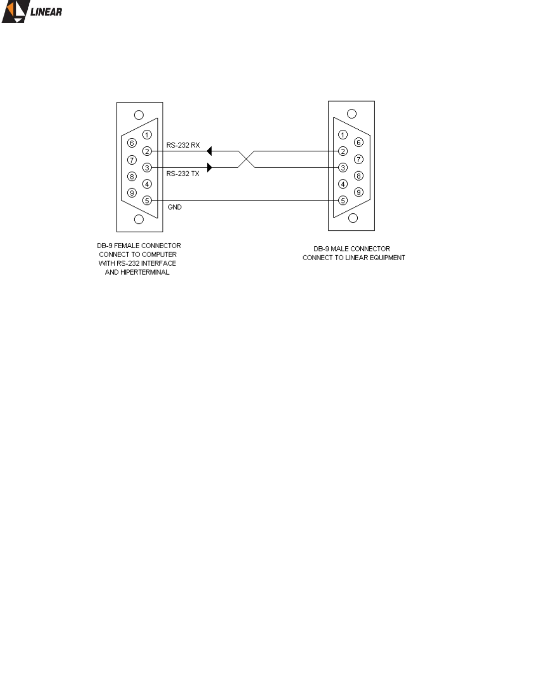
AT725P Owner’s Manual
© 2009 Linear Industries, Inc. All Rights Reserved AT725P_OM_08/09 68/75
Pin 3 is TX and pin 2 is RX. In the both connectors pin 5 is GND. The figure below illustrates the RS232
cable and connector:
The configuration of the Window® Hyper-terminal must in accordance with following:
PROPERTIES OF COM4
Configuration of Port
Bits per Second 19200
Bits of data 8
Parity None
Bits of Parity 1
Flow Control None
To access the data of the equipment and to bring up to date the screens in the Hyper-terminal use ENTER
on the keyboard. Screen 1 indicates some measurements, states of the alarms and offers options for access
to other functions of the equipment.
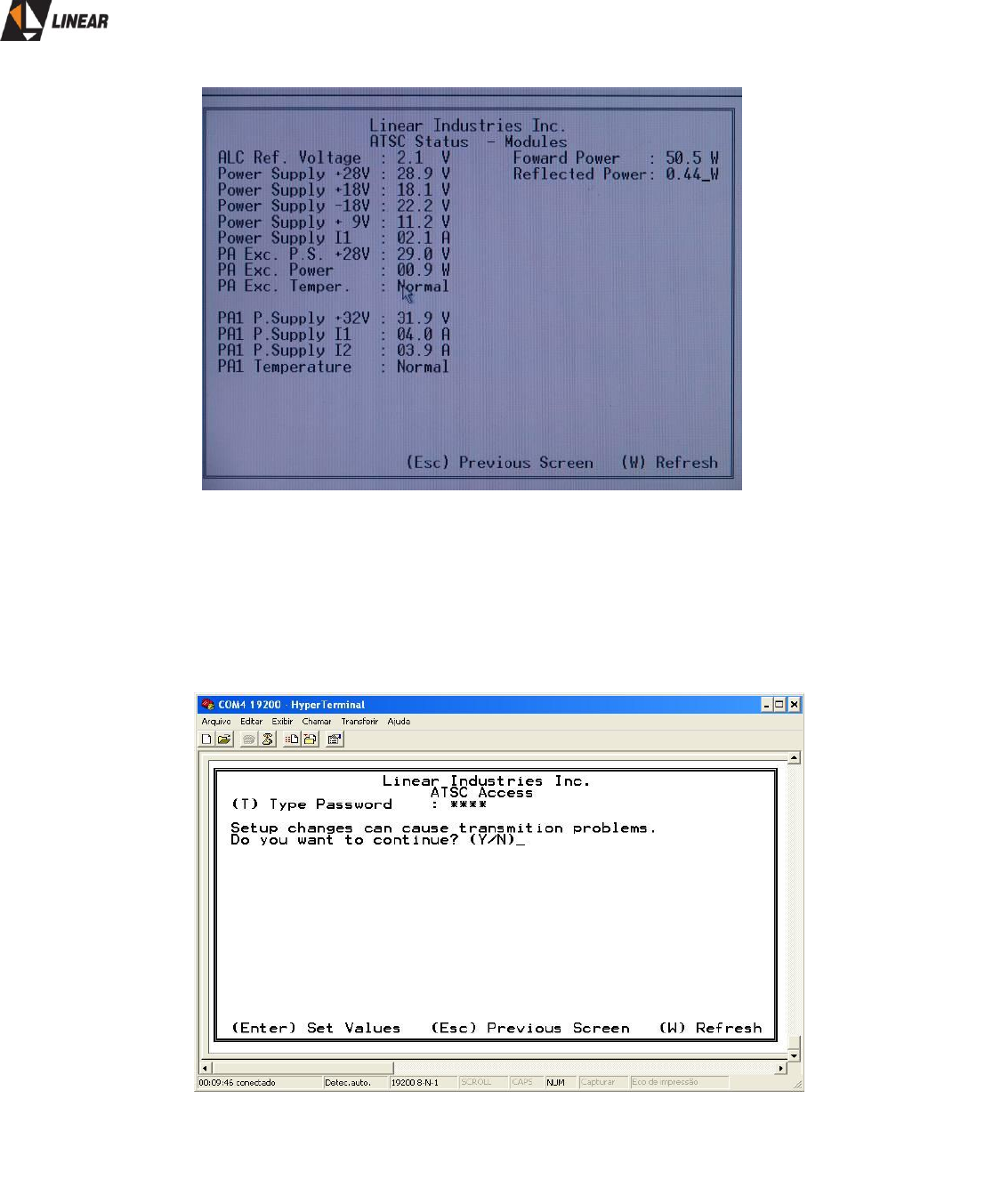
AT725P Owner’s Manual
© 2009 Linear Industries, Inc. All Rights Reserved AT725P_OM_08/09 69/75
When the password of the equipment is qualified screen 2 will be displayed. A password of 4 digits
must be entered to access the SETUP environment. In the case where the entered password is incorrect, the
message “WRONG PASSWORD" will be shown. When the password is correct a warning question is asked.
Reply YES (y), which then allows access to the SETUP environment. A NO (n) reply will return to the menu
to the previous screen 1.
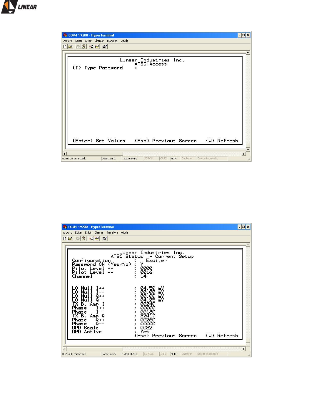
AT725P Owner’s Manual
© 2009 Linear Industries, Inc. All Rights Reserved AT725P_OM_08/09 70/75
To configure the parameters of screen 3 the characters in the parentheses should be selected by using
standard keyboard keys. Select the option desired and then use the keyboard characters U (up) and D
(down) or Y (Yes) or N (No) to display the values of configuration. For safety reasons the values entered are
only confirmed when exiting from the screen. Exit from the screen by using the ESC key. The W Key will
refresh the screen.

AT725P Owner’s Manual
© 2009 Linear Industries, Inc. All Rights Reserved AT725P_OM_08/09 71/75
Annex B – Checking the RF Power LDMOS Transistors
All 3 main RF transistors on the module 4408 are LDMOS technology type. The manipulation of these
transistors requires some special care, for instance avoiding manual bare finger direct contact with the parts.
Instead, prioritize the usage metal parts tools and grounded care procedures.
Gate-to-ground conductance test
With the transistors in place it is possible with a digital multimeter perform this test. Unplug the DC
connectors (CON-2 and CON-3) and measure the conductance between the gate terminal and ground.
T1:
Adjust TPO-1 for the minimum of its value; (all counterclockwise) the reading at the multimeter should be
close of 380Ω. Adjusting TPO-1 for the maximum of its value, the reading at multimeter should be close of
720Ω.
T2:
Adjust TPO-2 for the minimum of its value; (all counterclockwise) the reading at the multimeter should be
close of 370Ω. Adjusting TPO-1 for the maximum of its value, the reading at multimeter should be close of
720Ω.
T3:
Adjust TPO-3 for the minimum of its value; (all counterclockwise) the reading at the multimeter should be
close of 550Ω. Adjusting TPO-1 for the maximum of its value, the reading at multimeter should be close of
705Ω. These readings are expected remain the same for both T3 gates.
In event that these measurements does not comes true, check the possibility of some surrounding other
components be damaged, and/or proceed a careful visual inspection looking for abnormal circumstances .
Same tests suggested above could be repeated with the transistors detached out from the PCB board; on
this case measurement readings for gate-to-ground should be close of 40MΩ. Also on this situation detect a
diode type behavior measuring drain-to-source conductance as follows:
(+)
DRAIN
(-)
SOURCE
R=
580Ω
(+)
SOURCE
(-)
DRAIN
R=
∞
In case these 2 measurements cannot be verified, the transistor must be substituted.
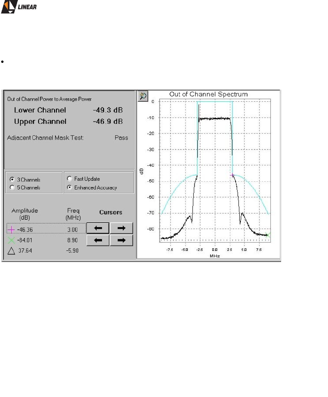
AT725P Owner’s Manual
© 2009 Linear Industries, Inc. All Rights Reserved AT725P_OM_08/09 72/75
Annex C – Typical Final Test Reports Results
Out of Channel Emissions
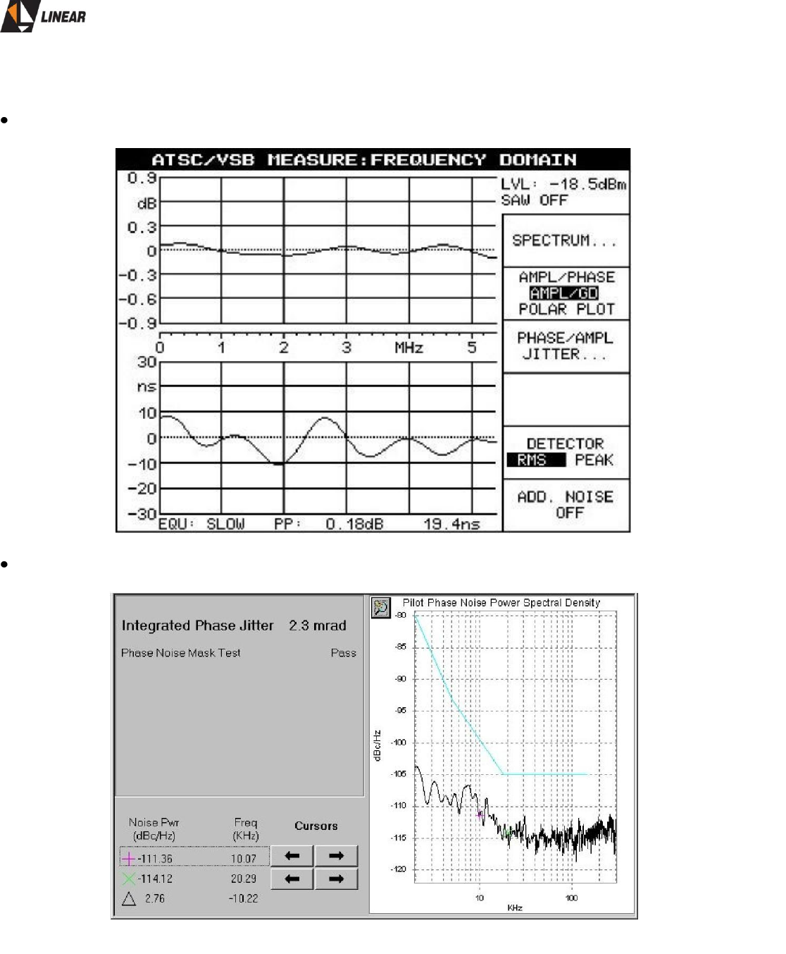
AT725P Owner’s Manual
© 2009 Linear Industries, Inc. All Rights Reserved AT725P_OM_08/09 73/75
Frequency Response and Group Delay
Carrier Phase Noise
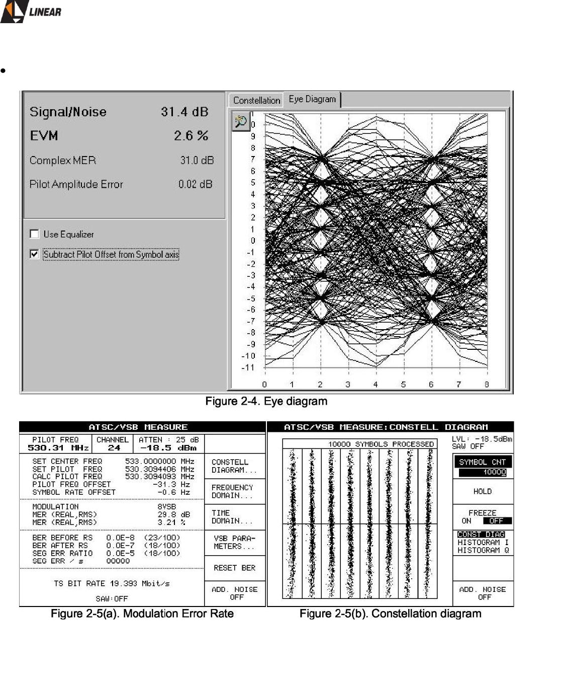
AT725P Owner’s Manual
© 2009 Linear Industries, Inc. All Rights Reserved AT725P_OM_08/09 74/75
Digital Modulation Error Rate:
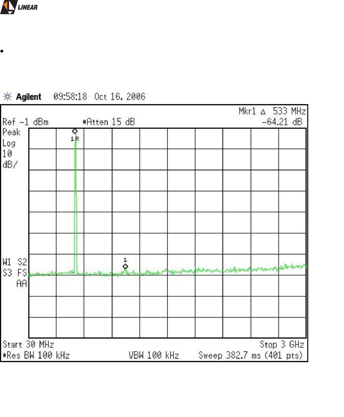
AT725P Owner’s Manual
© 2009 Linear Industries, Inc. All Rights Reserved AT725P_OM_08/09 75/75
Conducted Spurious Emissions