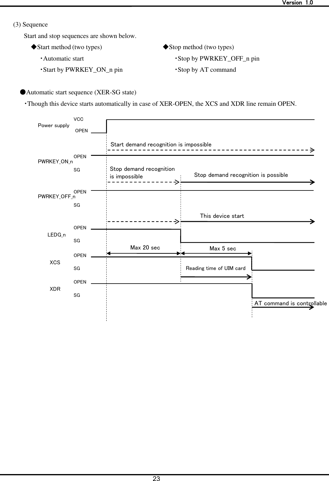
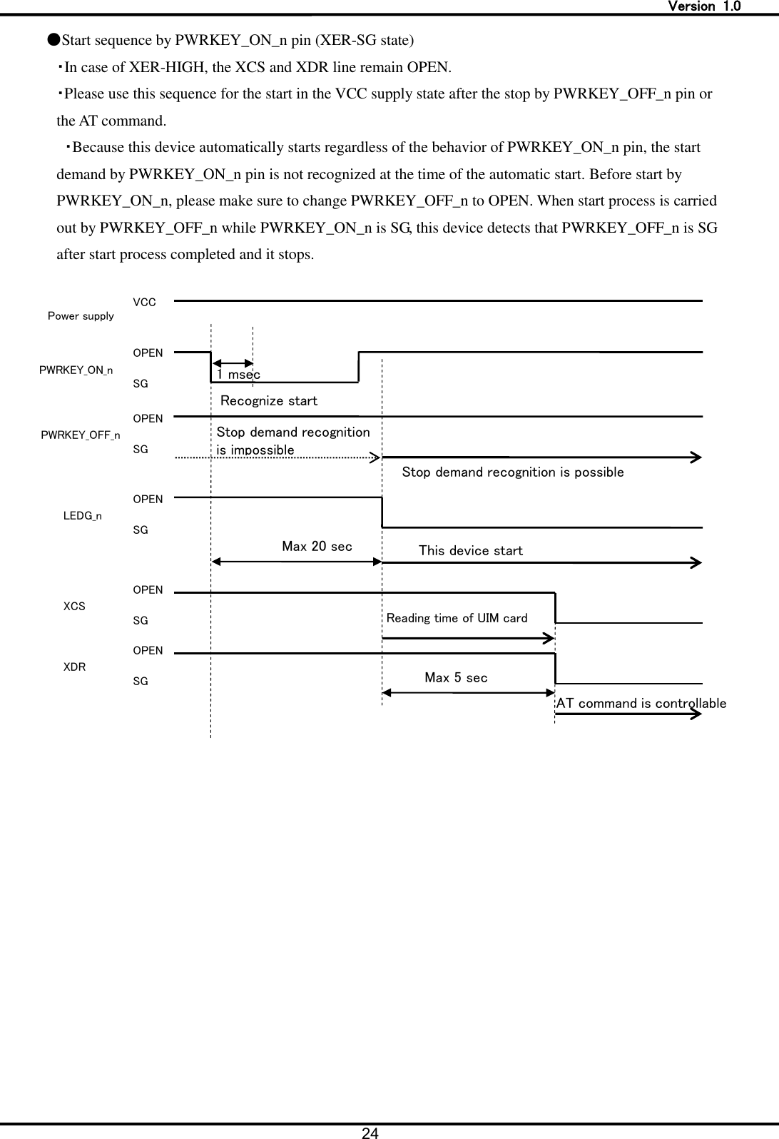
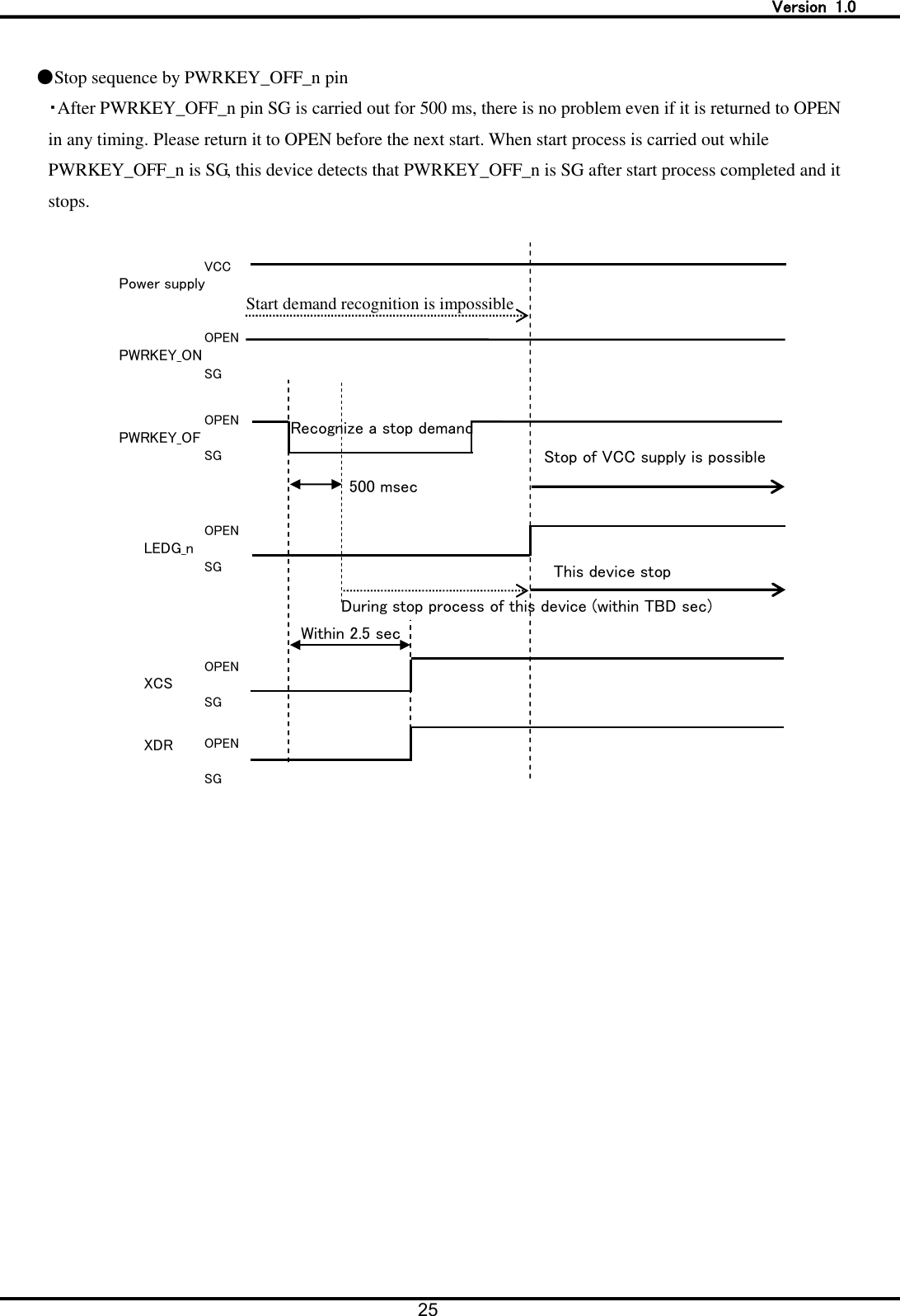
Hitachi Kokusai Electric UM04KO Wireless Communication Module User Manual
Hitachi Kokusai Electric Inc. Wireless Communication Module
UserManual.wiki
>
Hitachi Kokusai Electric
>
UM04KO User Manual
User Manual
Navigation menu
Upload a User Manual
Namespaces
Wiki Guide
HTML
PDF
Info
Views
User Manual
Discussion / Help
Navigation
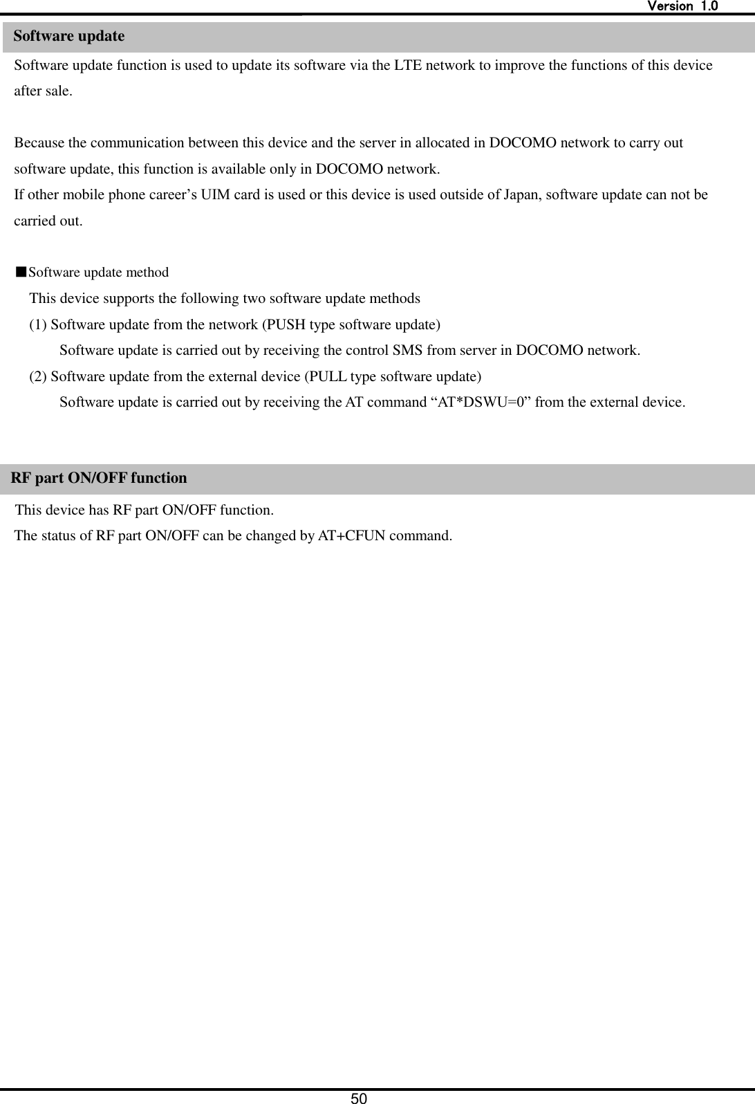
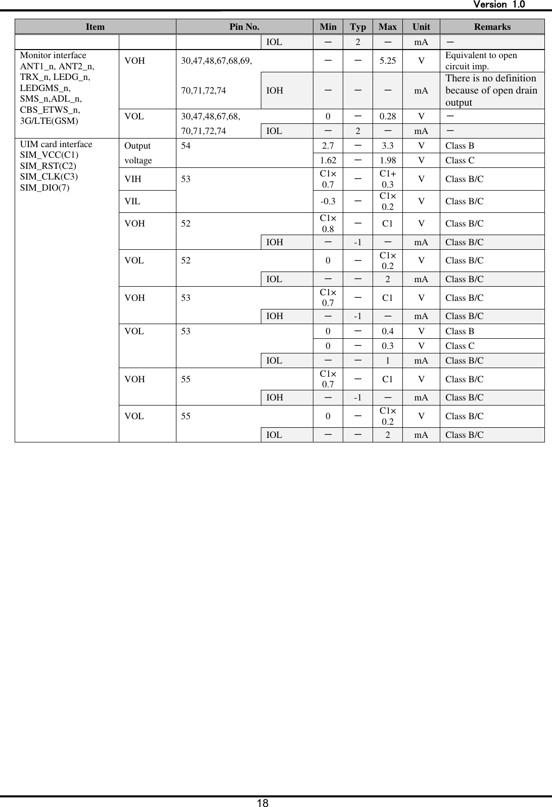
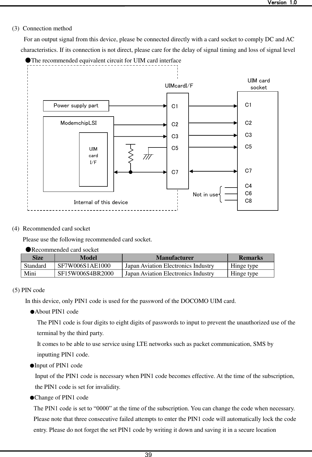
![Version 1.0 14 ■BtoB Connector This flexible connector is same as one used in UM03-KO. Connector specification Number of pins 80 Pin pitch 0.5 ㎜ Connection type Board to Board Connector Model number DF12(3.0)-80DS-0.5V(86) Manufacturer Hirose Electric CO., LTD. ◆Please use the connector shown in the following table for the external device which connected to this device. Connector specification Number of pins 80 Pin pitch 0.5mm Connection type Board to Board Connector Model number DF12B(3.0)-80DP-0.5V(86) Manufacturer Hirose Electric CO., LTD. ●Assignment of connector pins Connector Pin Type Pin No. Pin Name Signal Direction (UM04-KO⇔external device) Signal Function Setting of Unused pins Power supply 14 SG - Grounding Unconnection prohibited 18 SG - 21 SG - 31 SG - 34 SG - 37 SG - 38 SG - 39 SG - 40 SG - 51 SG - 41 VCC ← Power supply (3.3 to 4.2V) Unconnection prohibited 42 VCC ← 43 VCC ← 44 VCC ← 45 VCC ← 46 VCC ← 49 BtoB_DET(SG) - BtoB connection detection signal Unconnection prohibited [Note1] Power supply control 5 PWRKEY_ON_n ← Power ON request Open 6 PWRKEY_OFF_n ← Power OFF request Open 4 SYSRST_n ← System reset Open UARTserial interface 76 XCD → Carrier detection signal Open 80 XCI → Incoming call indication signal Open 78 XCS → Permission signal of sending from this device Open](https://usermanual.wiki/Hitachi-Kokusai-Electric/UM04KO/User-Guide-2755823-Page-14.png)
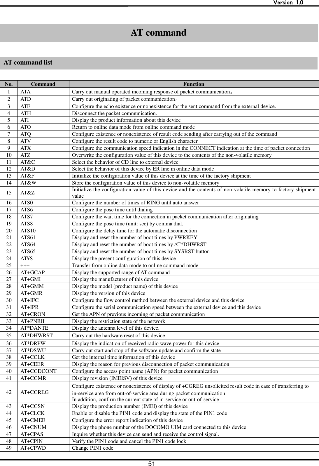
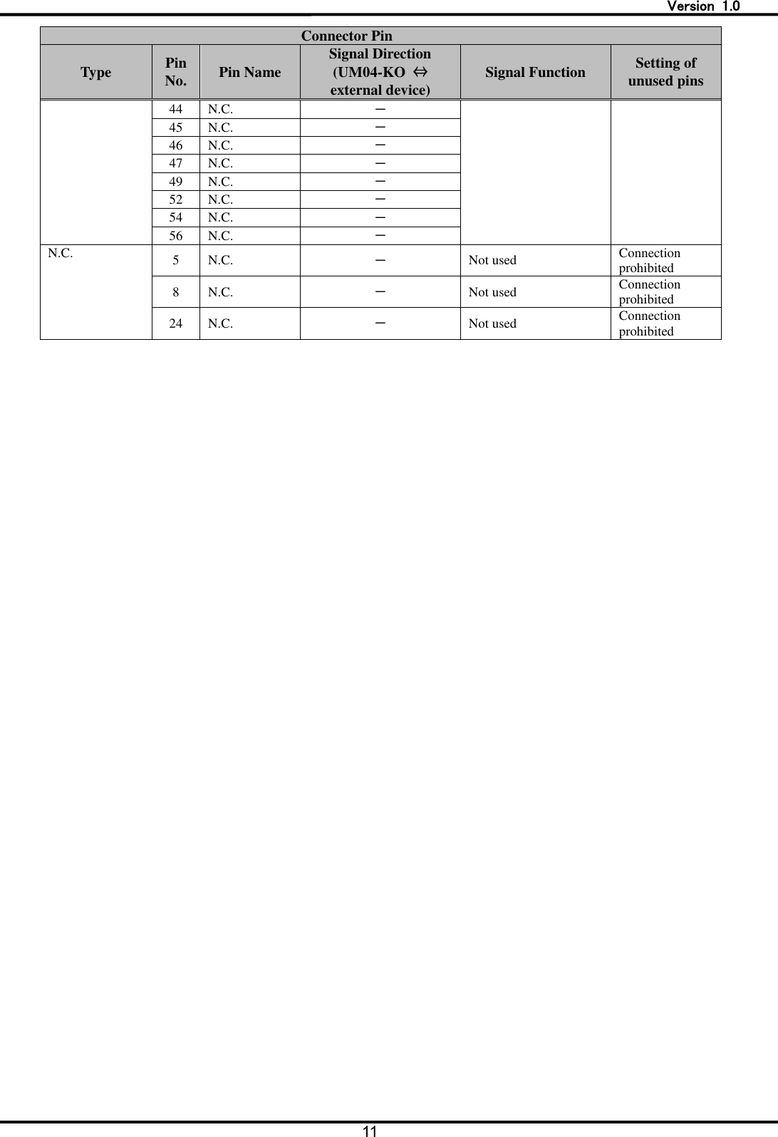
![Version 1.0 15 Connector Pin Type Pin No. Pin Name Signal Direction (UM04-KO⇔external device) Signal Function Setting of Unused pins 1 XRS ← Request signal of sending from external device Open [Note2] 3 XER ← Ready signal from external device Open [Note2] 79 XDR → Ready signal from this device Open 77 RD → Received data Open 2 SD ← Sending data Open [Note2] 10 DTE1 ← External device serial communication data speed configuration Depends on configured value 11 DTE2 ← 12 DTE3 ← モニタ インタフェース 71 ANT1_n → Antenna indication 1 Open 72 ANT2_n → Antenna indication 2 Open 70 TRX_n → Packet communication status indication Open 48 LEDG_n → Operation status indication Open 47 LEDGMS_n → Communication status indication Open 30 ADL_n → Software update status indication Open 68 SMS_n → Notification of SMS receiving Open 67 CBS_ETWS_n → Notification of Area Mail receiving Open 74 3G/LTE (GSM) → Attached network indication Open UIM card interface 54 SIM_VCC(C1) → Power supply Unconnection prohibited 52 SIM_RST(C2) → Reset Signal 55 SIM_CLK(C3) → Clock signal 56 SIM_GND(C5) - Grounding 53 SIM_DIO(C7) ⇔ Data input/output USB interface 20 USB_DPLUS ⇔ Data signal + Open 19 USB_DMINUS ⇔ Data signal - Open 23 USB_VBUS ← USB detection signal Open 22 USB_H_RDY_n ← Request of activation from external device Pull-down [Note3] 66 USB_D_RDY_n → Request of activation from this device Open Maintenance interface 17 N.C. - Manufacturer maintenance Connection prohibited 25 N.C. - 58 N.C. - 59 N.C. - 60 N.C. - 61 N.C. - 62 N.C. - 63 N.C. - 64 N.C. - 65 N.C. - 73 N.C. - N.C. 7 N.C. - Not used Connection prohibited 8 N.C. - 9 N.C. -](https://usermanual.wiki/Hitachi-Kokusai-Electric/UM04KO/User-Guide-2755823-Page-15.png)
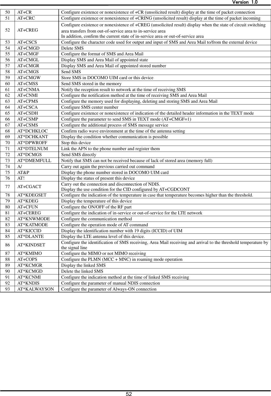
![Version 1.0 16 Connector Pin Type Pin No. Pin Name Signal Direction (UM04-KO⇔external device) Signal Function Setting of Unused pins 13 N.C. - 15 N.C. - 16 N.C. - 24 N.C. - 26 N.C. - 27 N.C. - 28 N.C. - 29 N.C. - 32 N.C. - 33 N.C. - 35 N.C. - 36 N.C. - 50 N.C. - 57 N.C. - 69 N.C. - 75 N.C. - [Note1] This signal is for the detection of BtoB connector connection. Please connect to SG without fail. [Note2] The connection of the pull-up resistor is no problem. In case of connecting the pull-up resistor, please use the power supply for pulling up within +1.8V to +5.25V. [Note3] Recommended resistor value of the pulling down is 10kΩ to 100kΩ. Direct connection with SG is no problem.](https://usermanual.wiki/Hitachi-Kokusai-Electric/UM04KO/User-Guide-2755823-Page-16.png)
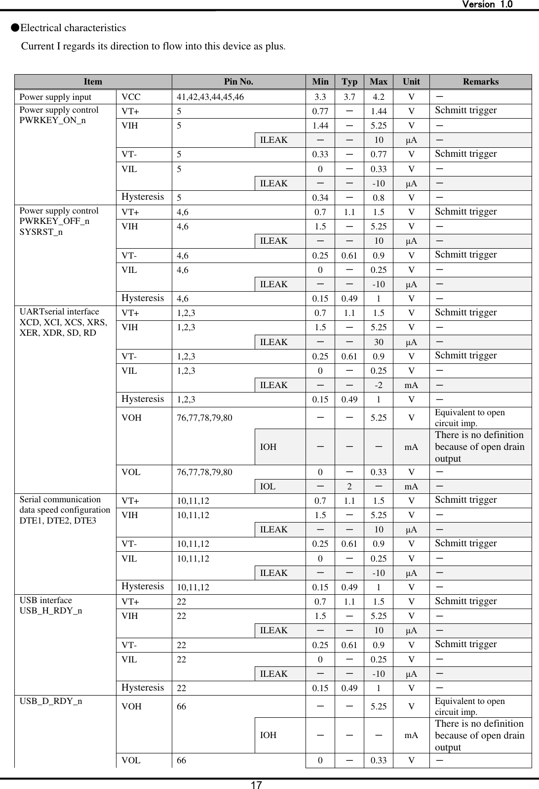
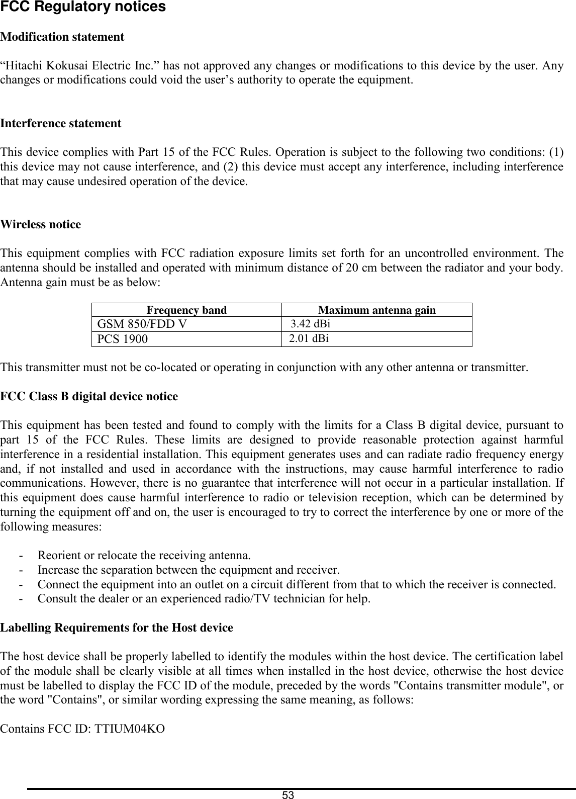
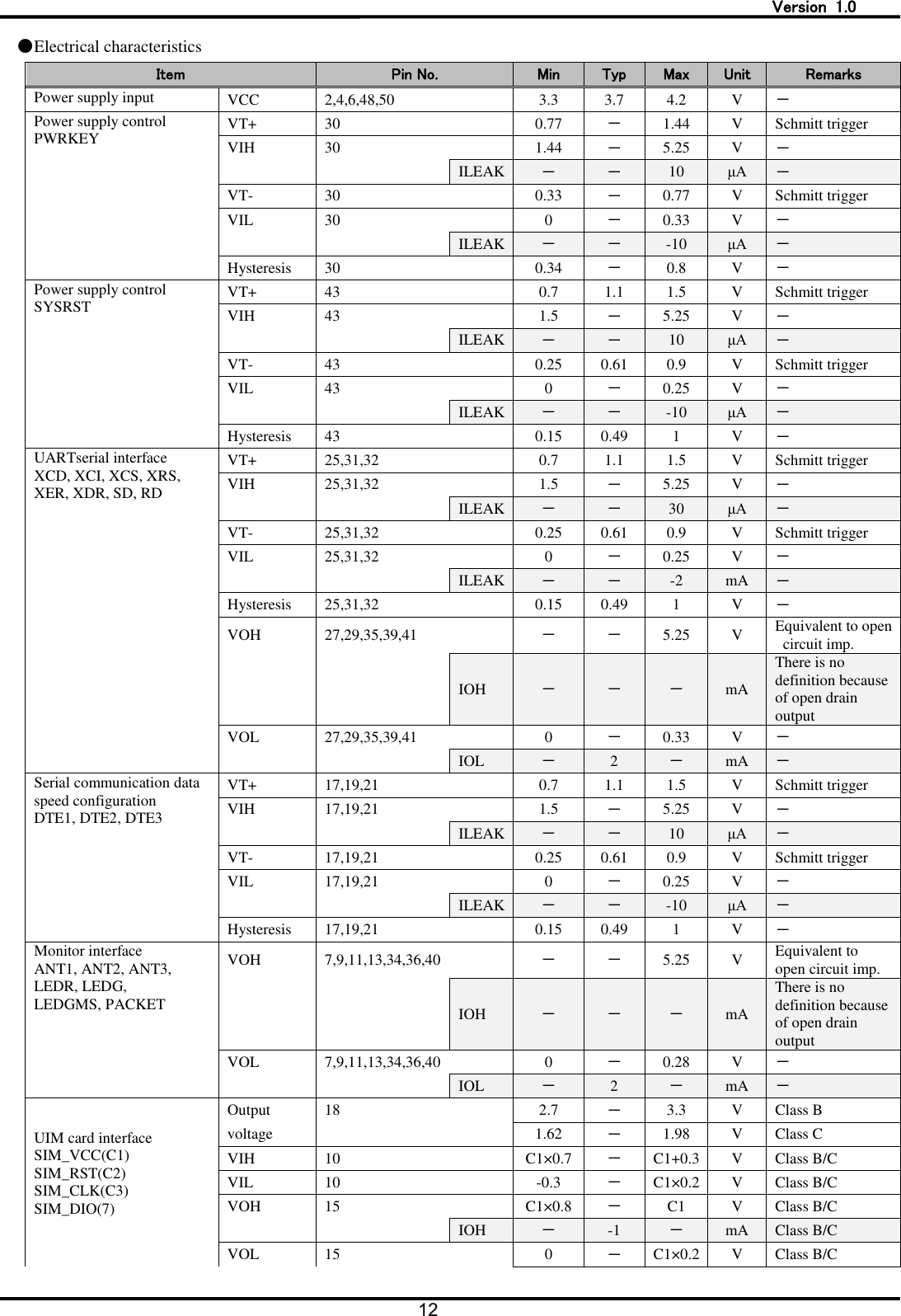
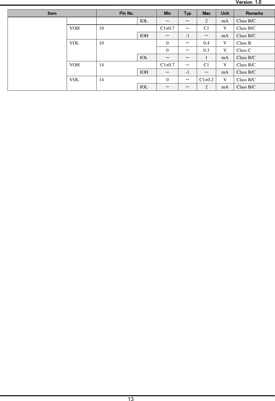
![Version 1.0 19 2.Power supply (1) Recommended specification for the external power supply Item Specification Voltage range DC+3.3V to +4.2V (Load condition: Steady supply in 0.1mA to 1,500mA) Ripple 50mVp-p (0Hz to 2.5GHz) or less Rating current 1,500mA or more Inrush current 2A (within 100μs) or less (2) Power supply input specification Pin name Min Typ Max Unit Remarks VCC +3.3 +3.7 +4.2 V - (3) Transient specification of the power supply voltage rising Pin name Min Typ Max Unit Remarks VCC - - 50 msec Refer to the following figure for waveform. ●Transient waveform of power supply voltage rising T[msec] 50msec Steady supply 4.2 3.7 3.3 VCC[V] 0](https://usermanual.wiki/Hitachi-Kokusai-Electric/UM04KO/User-Guide-2755823-Page-19.png)
![Version 1.0 28 3.UART interface The specification of the UART is shown below Item Specification Signal line SD, RD, XER, XDR, XRS, XCS, XCD, XCI Communication data speed [bps] 1200/2400/4800/9600/19200/38400/57600/115200/230400/460800 Configuration method of communication data speed External pins (DTE1, DTE2, DTE3), AT command Communication format Start:1bit, Stop:1bit, Data:8bit, Parity:none Sending/Receiving control hardware flow control, software flow control, and without flow control Detection of escape +++ (guard time is specified) Detection of break None Baud rate deviation Sending:2% or less Receiving:2% or less ■Configuration of serial communication data speed by AT command Only when the configuration of serial communication data speed by DTE1, DTE2 and DTE3 is 19200 [bps], the configuration by AT command can be used. ●The serial communication data speed configured by AT+IPR Serial communication data speed[bps] Remarks 1 1200 - 2 2400 - 3 4800 - 4 9600 - 5 19200 Initial value 6 38400 - 7 57600 - 8 115200 - 9 230400 - 10 460800 -](https://usermanual.wiki/Hitachi-Kokusai-Electric/UM04KO/User-Guide-2755823-Page-28.png)
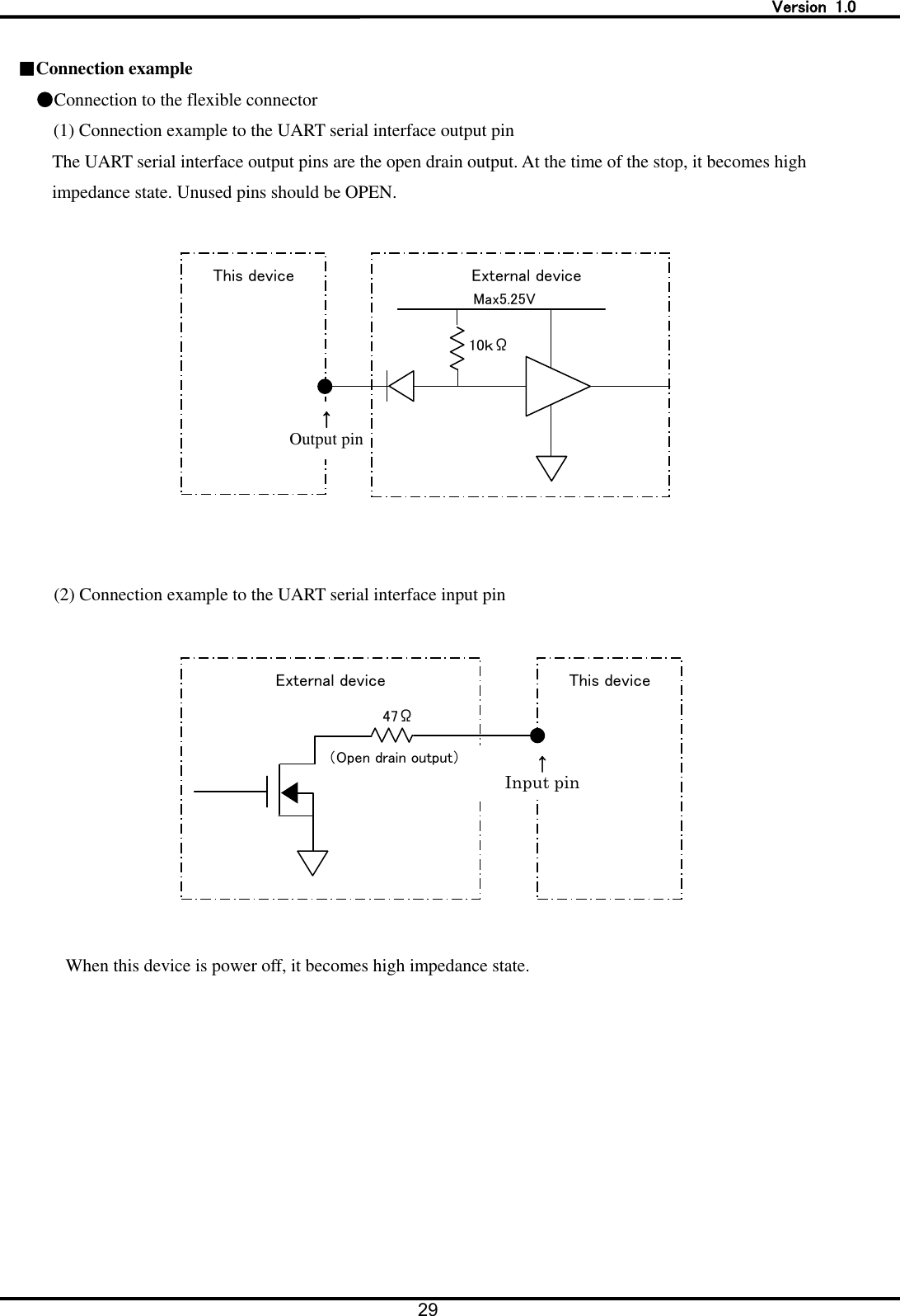
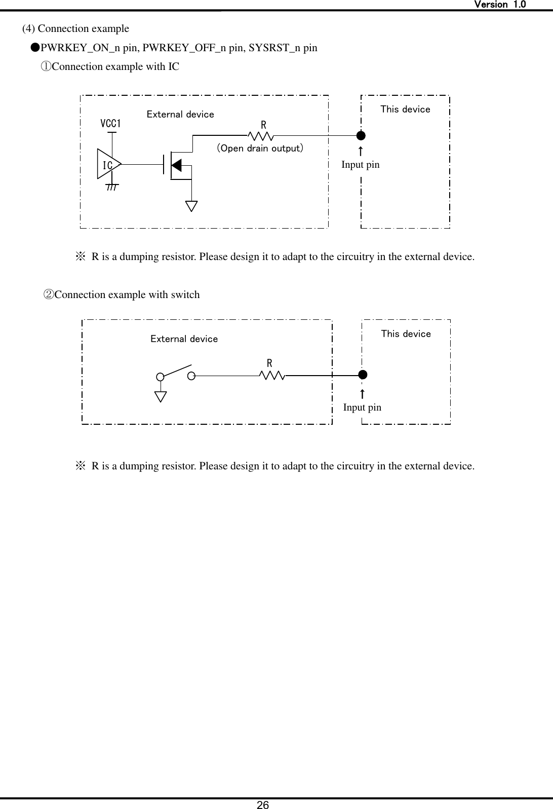
![Version 1.0 30 ●Connection to BtoB connector (1) Connection example to the UART serial interface output pin (XCD、XCI、XCS、XDR、RD) The UART serial interface output pins are the open drain output. At the time of the stop, it becomes high impedance state. Unused pins should be OPEN. [Note] R is pull-up resistor. Please design it to adapt to the circuitry in the external device. (2) Direct Connection example to the UART serial interface input pins (XRS, XER, SD, DTE1, DTE2, DTE3) The input pins are the Schmitt trigger input with tolerant of 5V ●Direct connection example to the UART serial interface input pins [Note] R is pull-up resistor. Please design it to adapt to the circuitry in the external device. This device ↑ Output pin R External device +1.8V~+5V R This device ↑ Input pin IC External device](https://usermanual.wiki/Hitachi-Kokusai-Electric/UM04KO/User-Guide-2755823-Page-30.png)
![Version 1.0 31 ●Open drain connection example to the UART serial interface input pins Please input the open drain output when the external device which can not meet DC characteristic is connected. [Note] R1 is pull-up resistor and R2 is dumping resistor. Please design it to adapt to the circuitry in the external device. ●Connection example to DTE1、DTE2、DTE3 input pins When fixed serial communication data speed is used, please fix the level by pull-up or pull-down depending on configuration value. [Note] R1 is pull-up resistor and R2 is pull-down resistor. Please design it to adapt to the circuitry in the external device. [Requirement of SD pin and RD pin] (1) Requirement of SD pin (input) ①When the external device which is connected to SD pin can not meet DC characteristic, it is necessary to be connected by the open drain output. Dull of wave pattern caused by connection of the open drain output may cause data communication failure. Therefore, requirement for the input waveform for the connection of the open drain output is specified. R2 +1.8V~+5V R1 This device ↑ Input pin (Open drain output) IC VCC1 External device R1 +1.8V~+5V R2 Pull-up This device ↑ Input pin Pull-down ↑ Input pin External device](https://usermanual.wiki/Hitachi-Kokusai-Electric/UM04KO/User-Guide-2755823-Page-31.png)
![Version 1.0 32 ②For the requirement for SD pin input waveforms, the ratio per one bit of data which is measured in voltage level of SG interval [A] and OPEN interval [B] should be adjusted within from 50:50 to 56:44. ・This requirement is applied for the waveform that was measured at the most close point to the main connector. ・The slope of the rising wave pattern depends on the circuitry of the external device. In case that the dull of the wave pattern is big and the ratio of SG is wider, for example, please adjust it so that the dull of the wave pattern becomes small to reduce the pull-up resistor value. ●SD pin (input) wave pattern ●Waveform measurement point of UART serial receiving data (SD pin) (2)Requirement of RD pin (output) ①The RD pin is the open drain output. ②Dull of rising wave pattern may cause any failure. Please confirm it each external devices to be connected. In case that the dull of the wave pattern is big, for example, please adjust it in external device so that the dull of the wave pattern becomes small to reduce the pull-up resistor value. SD pin Vt+(Max)1.29V 【A】 【B】 Vt-(Max)0.67V Vt-(Max)0.67V Assume this section 100 The ratio of 【A】 and 【B】 Within from 50:50 to 56:44 Vt+:The OPEN level threshold voltage of this device Vt-:The SG level threshold voltage of this device This device External device Main connector Circuit Measurement point](https://usermanual.wiki/Hitachi-Kokusai-Electric/UM04KO/User-Guide-2755823-Page-32.png)
![Version 1.0 33 4.USB interface The USB interface of this device is based on USB 2.0 specification. The transmission and reception of data is possible as a USB device. You can use it for the control by the AT command. The connection with the USB host is disconnected when you make reboot (power off / on, reset by AT*DHWRST). Item Specification Communication standard Conformity USB2.0 (Device) Communication speed FULL SPEED (12Mbit/s), 、HIGH SPEED (480Mbit/s) Signals USB_DPLUS, USB_DMINUS, USB_VBUS, USB_H_RDY_n, USB_D_RDY_n Virtual COM port Port1 : Modem control Port2 : Network card control ■Connection example (1) USB interface pin (USB_DPLUS, USB_DMINUS, USB_VBUS) ●Connection example to the external device [Note] USB_VBUS does not mean power supply of 5V from a host, and it mean a USB host connection state. (2)USB_D_RDY_n output pin This output pin is the open drain output. At the time of the stop of this device, it becomes the high impedance state. In case of unused condition, set a pin as OPEN. ●Connection example to USB_D_RDY_n output pin This device USB_DPLUS USB_DMINUS USB_VBUS SG USB host External device](https://usermanual.wiki/Hitachi-Kokusai-Electric/UM04KO/User-Guide-2755823-Page-33.png)
![Version 1.0 34 [Note] R is pull-up resistor. Please design it to adapt to the circuitry in the external device. (3)USB_H_RDY_n input pin The input composes it of Schmidt trigger of 5V tolerant. When you connect the external device which cannot meet DC characteristics, it is necessary to input at this device by the output of the open drain. ●Direct connection example to USB_H_RDY_n input pin [Note] R is dumping resistor. Please design it to adapt to the circuitry in the external device. ●Open drain connection example to USB_H_RDY_n input pin [Note] R1 is pull-up resistor and R2 is dumping resistor. Please design it to adapt to the circuitry in the external device. This device R ↑ Output pin External device +1.8V~+5V R This device ↑ Input pin IC External device +1.8V~+5V R1 R2 This device ↑ Input pin (Open drain output) External device IC VCC1](https://usermanual.wiki/Hitachi-Kokusai-Electric/UM04KO/User-Guide-2755823-Page-34.png)
![Version 1.0 36 ■Communication state indication Communication state is indicated based on the combination of TRX_n, LEDG_n and LEDGMS_n. ●Communication state indication specification State TRX_n LEDG_n LEDGMS_n Remarks 1 In operation During stand-by OPEN SG OPEN - 2 During communication SG SG OPEN 3 During incoming OPEN SG SG⇔OPEN [Note1] 4 During software update During download Depends on communication state SG Depends on communication state - 5 During rewriting (SW update mode 3) OPEN SG OPEN - 6 During reboot (SW update mode 3) OPEN OPEN OPEN - 7 During the update completion notification transmitting (SW update mode 3) Depends on communication state SG Depends on communication state - 8 Stop state of this device OPEN OPEN OPEN - [Note1] Waveform of LEDGMS_n is shown below during incoming. ●Waveform of LEDGMS_n signal during incoming ■Software update state indication Software update state is indicated by ADL_n signal. ●Software update state indication specification State ADL_n (NW reservation type) ADL_n (AT command type) Remarks 1 During software update During download OPEN SG - 2 During rewriting (SW update mode 3) SG SG - 3 During reboot (SW update mode 3) OPEN OPEN - 4 During the update completion notification transmitting (SW update mode 3) SG SG - 5 During other than software update OPEN OPEN - OPEN SG 0.2±0.01[s] 1.8±0.01[s] 1.2±0.01[s] 1cycle:3.0±0.01[s] LEDGMS_n](https://usermanual.wiki/Hitachi-Kokusai-Electric/UM04KO/User-Guide-2755823-Page-36.png)
![Version 1.0 37 ■SMS receiving indication The receiving of SMS is indicated by SMS_n. ●SMS receiving indication specification State SMS_n Remarks 1 Receiving SMS OPEN→SG→OPEN - 2 Other than SMS receiving OPEN - ●Waveform of SMS_n when a SMS is received ■Area Mail receiving indication The receiving of Area Mail is indicated by CBS_ETWS_n. ●Area Mail receiving indication specification State CBS_ETWS_n Remarks 1 Receiving Area Mail OPEN→SG→OPEN - 2 Other than Area Mail receiving OPEN - ●Waveform of CBS_ETWS_n when an Area Mail is received ■Connection example The monitor interface of this device is the open drain output. ●A connection example of the external LED lamp to monitor interface At the time of the stop of this device, it becomes the high impedance state. ※R is a pull-up resistor. Please assume it a value to adapt to a circuitry of the external device OPEN SG 90[ms] or more CBS_ETWS_n This device R ↑ Output pin External device OPEN SG 90[ms] or more SMS_n](https://usermanual.wiki/Hitachi-Kokusai-Electric/UM04KO/User-Guide-2755823-Page-37.png)
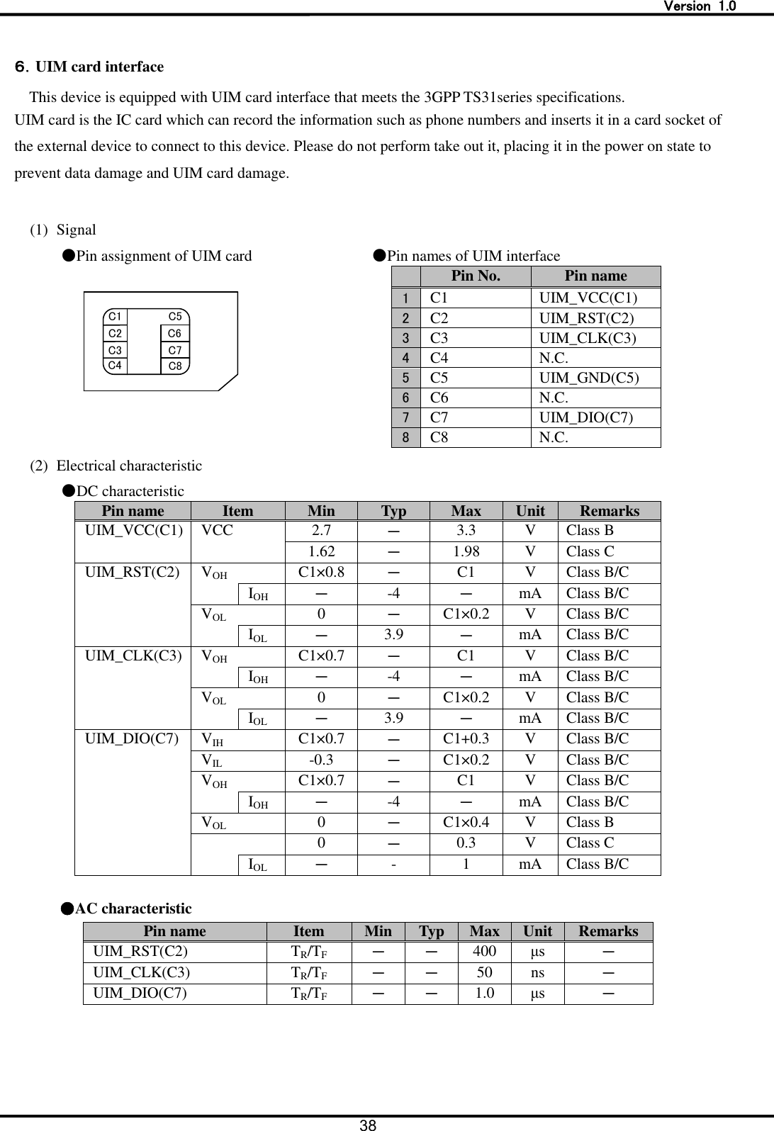
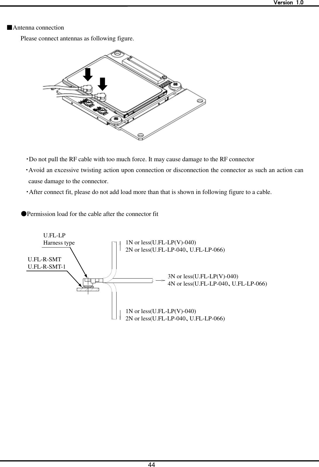
![Version 1.0 40 ●About PIN1 unlock code The PIN1 unlock code is used to clear the locked state of the PIN1 code. This code will be provided to the customer at the time of the subscription. Entering the eight digits PIN1 unlock code clears the locked state. Note that ten consecutive failed attempts to enter the PIN1 unlock code will automatically lock the code entry. If you forget the PIN1 unlock code or when the PIN1 code lock can not be cleared, please contact the customer service. 7.RF connector (Main/Sub) This device is equipped with RF connectors to connect the antenna. ■Used connector ●A model name and the manufacturer name of the RF connector are shown below RF connector (This device side) RF connector [Note1] (External device side) Model name U.FL-R-SMT U.FL-LP-040 U.FL-LP-066 Manufacturer Hirose Electric CO., LTD Hirose Electric CO., LTD [Note1] Confirm the details with the manufacturer, as the part number will be different depending on the diameter of the used cable. ■Pin assignment ●Pin assignment Signal No. Pin name Description Signal Direction (This device ⇔ Antenna) Remarks TRX connector (Main) Transmit and receive 1 TRX Transmit and receive signal ⇔ 2GHz/800MHz RF signals 2 SG Grounding - - TRX connector (Sub) Receive 1 TRX Receive signal ⇔ 2GHz/800MHz RF signals 2 SG Grounding - - Pin1(Signal pin) Pin2 (SG)](https://usermanual.wiki/Hitachi-Kokusai-Electric/UM04KO/User-Guide-2755823-Page-40.png)
![Version 1.0 41 8.External antenna ・The external antenna (optional product) of DOCOMO can be used as the external antenna to be connected to this device. ・Plural antennas, which are main antenna (for transmit and receive) and sub antenna (for receive), can be connected. ・About the selection of use of the plural or single antenna, it can be configured by the command “AT*KMIMO” which is the AT command to select MIMO receiving or not MIMO receiving. ・If “not MIMO receiving” is selected, this device can be in operation with single antenna. In that case, please connect the external antenna to main antenna connector. ●External antennas of the optional products (Sale product particularly) of DOCOMO Name Connector type Remarks 1 Roof-top antenna for FOMA adaptor 02 SMA-P Dual band (2 GHz/800 MHz) antenna Supplied with an antenna cable (about 5.5 meters long) 2 Simple antenna for FOMA adaptor SMA-P Dual band (2 GHz/800 MHz) antenna Supplied with an antenna cable (about 5.0 meters long) 3 Compact water-proof antenna for FOMA adaptor SMA-P Dual band (2 GHz/800 MHz) antenna Supplied with an antenna cable (about 2.5 meters long) The connector adaptation methods (U.FL to SMA) for connecting this device to the antenna recommended in the above list are shown below, with examples of adaptor types. As the method of connector adaptation, you can use either an adaptor cable or a combination of an adaptor connector and an RF cable. Please refer to the manufacturer for the specification of cable and connector. [Adaptor cable] This adaptor cable is used to converts RF connector (U.FL female) into a SMA-male. Model number Manufacturer Type Remarks HRMJ-U.FL-066N1-A-100RS Hirose Electric CO., LTD U.FL female to SMA female Cable length 100mm [RF cable and adaptor connector] ●RF cable Model number Manufacturer Type Remarks U.FL-2LP-04K2T-A-(80) Hirose Electric CO., LTD U.FL female to U.FL female Cable length 80mm Cable color black ●Adaptor connector Model number Manufacturer Type Remarks HRMJ-U.FLJ-PC-1 Hirose Electric CO., LTD U.FL male to SMA female For direct connection to the circuit board.](https://usermanual.wiki/Hitachi-Kokusai-Electric/UM04KO/User-Guide-2755823-Page-41.png)
![Version 1.0 45 Operation mode Communication mode This device supports three communication modes. Only in roaming mode, this device supports the communication method selection function. ●Supported communication mode Communication mode Description Remarks LTE mode (fixed) Operated in LTE network only in Japan Default Roaming mode (fixed) Operated out of Japan. [Note1] Auto selection mode Select the communication mode (LTE or Roaming) automatically [Note1] Only in roaming mode, the communication method can be configuration by AT*KNWMODE. Communication modes which can be selected are dual of WCDMA+GSM (default), WCDMA single and GSM single. ・If flexible connector is used to connect to the external device, then only LTE mode can be available. ・Communication mode and method can be changed by AT command. And the configuration is stored in this device. ・After the communication mode is changed by AT command, please reboot this device ・This device reports the UE Capability corresponding with the selected communication mode to the network. ●LTE mode ◆Supported communication method : LTE ◆Supported mobile phone career : only NTT DOCOMO ◆Roaming operation : None (Because LTE mode is used only in Japan) ●Roaming mode ◆Supported communication method : WCDMA, GSM Configuration can be dual of WCDMA+GSM or WCDMA single or GSM single. ◆Supported mobile phone career : Mobile phone career out of Japan Operation mode Communication mode](https://usermanual.wiki/Hitachi-Kokusai-Electric/UM04KO/User-Guide-2755823-Page-45.png)