Hitachi Kokusai Electric UM04KO Wireless Communication Module User Manual
Hitachi Kokusai Electric Inc. Wireless Communication Module
User Manual
Version 1.0
LTE Ubiquitous Module®(UM04-KO)
Instruction Manual
Version 1.0
August 2015

Version 1.0
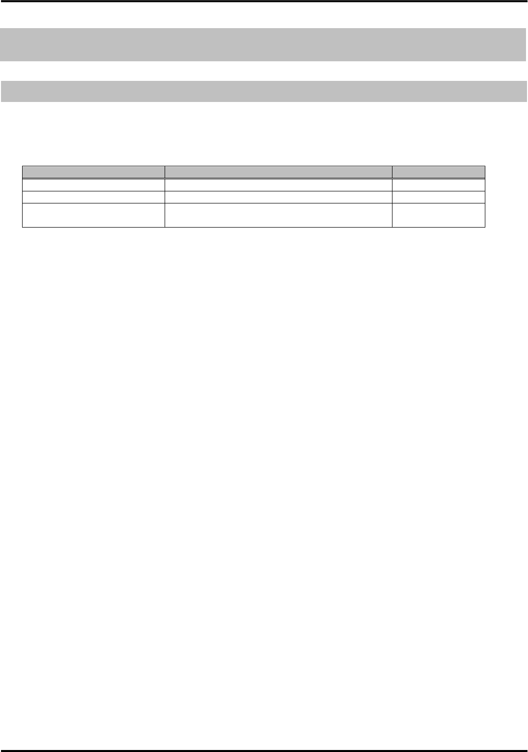
― Contents ―
Introduction ...................................................................................................................................................................................................... 3
■Dimensional outline drawing ............................................................................................................................................................ 4
■Interface for the external device ...................................................................................................................................................... 5
■Available services with this device .................................................................................................................................................. 6
Device specification ...................................................................................................................................................................................... 7
Main specification.......................................................................................................................................................................................... 7
Interface ........................................................................................................................................................................................................ 9
1.Main connector ............................................................................................................................................................................... 9
2.Power supply ................................................................................................................................................................................. 19
3.UART interface ............................................................................................................................................................................ 28
4.USB interface ................................................................................................................................................................................ 33
5.Monitor interface ......................................................................................................................................................................... 35
6.UIM card interface ..................................................................................................................................................................... 38
7.RF connector (Main/Sub) ......................................................................................................................................................... 40
8.External antenna ......................................................................................................................................................................... 41
Precautions for connecting to the external device .......................................................................................................................... 42
Precaution for design of the external device .................................................................................................................................. 42
Recommended installation method ..................................................................................................................................................... 43
■In case of using the flexible connector ................................................................................................................................... 43
■In case of using the BtoB connector ........................................................................................................................................ 43
■Antenna connection ...................................................................................................................................................................... 44
Operation mode ............................................................................................................................................................................................ 45
Communication mode .............................................................................................................................................................................. 45
Service function ........................................................................................................................................................................................... 47
Packet communication ........................................................................................................................................................................... 47
SMS .............................................................................................................................................................................................................. 49
Area Mail ..................................................................................................................................................................................................... 49
Software update ....................................................................................................................................................................................... 50
RF part ON/ OFF function .................................................................................................................................................................... 50
AT command ................................................................................................................................................................................................. 51
AT command list....................................................................................................................................................................................... 51

Version 1.0
3
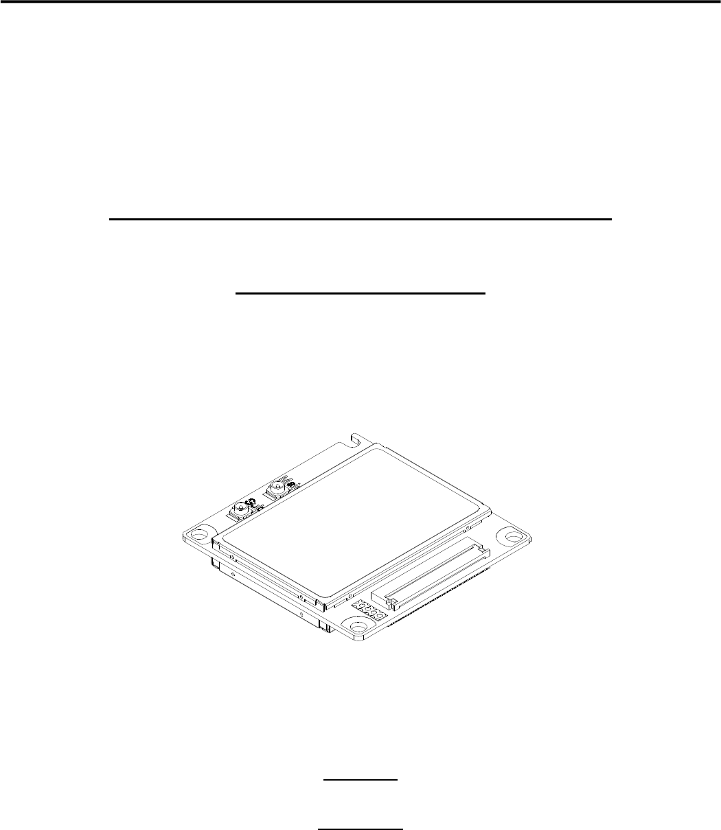
Introduction
Please note that “UM04-KO” is referred to as “this device” in this instruction manual.
This device is the communication module which unified in combination with the radio part of the cellular telephone
and the modem part.
This device has the functions of packet communication and SMS.
As this device is built-in to the external device product, the LTE communication service (only in Japan) and
W-CDMA/GSM communication service (out of Japan) can be used.
This device is an environment-conscious product which is compliant with the RoHS Directive.
Introduction
Version 1.0
4
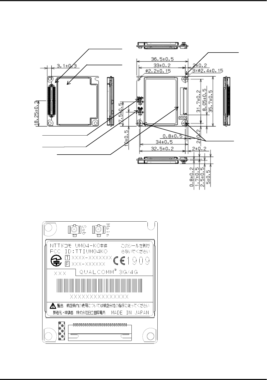
■Dimensional outline drawing
●Name plate seal outline drawing
RF connector (MAIN)
コネクタ
Shield case
(Insulation label)
Mounting hole
Mounting hole
Main connector (BtoB)
Main connector (flexible)
RF connector (SUB)
Unit: mm
Version 1.0
5
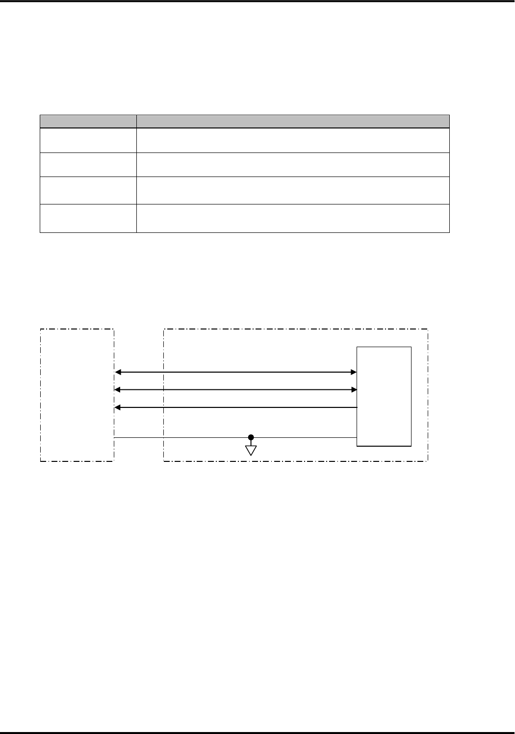
■Interface for the external device
●Interface between this device and the external device (A-side : Flexible connector)
●Interface between this device and the external device (B-side : BtoB connector)
This device has two main connectors. One is flexible connector on A-side and another is BtoB connector on
B-side. They each contain the interface of power supply, UART , USB (only in case of BtoB connector), UIM
card. RF connectors on A-side are used to connect the external antennas.
UIM card
Main connector
(flexible connector)
・Power supply
・Power supply Control
・UARTserial interface
・Monitor interface
・UIM card interface
External device
This device
(A-side)
RF connector (Sub)
RF connector (Main)
UIM card
Main connector
(BtoB connector)
・Power supply
・Power supply Control
・UARTserial interface
・USB interafce
・Monitor interface
・UIM card interface
External device
This device
(B-side)

Version 1.0
6
■Available services with this device
This device can use various communication services of DOCOMO. Packet communication, SMS and other
associated various services are available.
In addition, for the use of the service, production of the external device which incorporated this device is necessary.
●Packet communication
Packet communication (packet switching) is communication method that transmits and receives divided data
which is partitioned into the unit of called packet (package).
Because the packet communication can use one line in common by plural external devices or applications, it can
communicate efficiently.
The data communication speed is 112.5Mbps for downlink and 37.5Mbps for uplink (best effort type) in LTE
network, and 42.2Mbps for downlink and 5.7Mbps for uplink (best effort type) in W-CDMA network.
●SMS
SMS (short message service) is the service that can transmit and receive the letter message of the short sentence
easily with the address which is same to phone number regardless of the mobile phone career through SMS center
of DOCOMO.
●Area Mail
Early warning “Area Mail” service is the service in Japan that earthquake early warning and tsunami warning
from Japan Meteorological Agency and the disaster and the refuge information from the country and the regional
public institution are delivered to cellphones and communication models which exist in the particular area all at
once through the DOCOMO network.
Please refer to the website of DOCOMO for the regional public institution which started service of the disaster
and the refuge information using Area Mail.
This device can not receive Area Mail at the place of weak radio wave.
During packet and other communication, it may receive Area Mail depending on communication situation. In
addition, it can not receive the Area Mail again that it missed to receive.
The reception of Area Mail is free of charge.
●Software update
This is the function to update the software of this device in LTE network after sale.
Version 1.0
7
Device specification
Main specification
Item
Description
Remarks
LTE mode
(LTE method)
Roaming mode
(W-CDMA/GSM method)
Supported service
Packet communication, SMS
-
Communication protocol
PPP, IP
-
Control method
AT command
-
UART serial
interface
Number of ports
One line
-
Signals
SD、RD、XER、XDR、XRS、XCS、XCD、XCI
-
Communication
speed (bps)
1200/2400/4800/9600/19200/38400/
57600/115200/230400/460800
-
Communication
format
Start:1bit, Stop:1bit, Data:8bit, Parity:none
-
Sending/Receivin
g control
Support hardware flow control, software flow control,
and without flow control
-
Baud rate
deviation
Sending:2% or less
Receiving:2% or less
-
USB interface
Communication
standard
Conformity USB2.0
Supported in case of BtoB
connector
Number of ports
One line
Function
Device function
Communication
speed
HS:480Mbps, FS:12Mbps
Signals
USB_DPLUS、USB_DMINUS、USB_VBUS、
USB_D_RDY_n、USB_H_RDY_n
RF interface
Radio frequency
2GHz/800MHz Band
【W-CDMA method】
2GHz/800MHz Band
【GSM method】
GSM850MHz/ GSM900MHz/
GSM1800MHz/
GSM1900MHz
-
Access method
OFDMA, SC-FDMA
【W-CDMA method】
DS-CDMA, T-HCDMA
【GSM method】
TDMA
-
Data
communication
speed
Uplink :37.5Mbps Max
Downlink :112.5Mbps
Max
【W-CDMA method】
Uplink : 5.7Mbps Max
Downlink: 42.2Mbps Max
【GSM method】
Uplink : 237kbps Max
Downlink: 237kbps Max
Best effort type
Monitor
interface
BtoB connector
ANT1_n, ANT2_n, TRX_n, LEDG_n, LEDGMS_n, ADL_n、
3G / LTE (GSM), SMS_n, CBS_ETWS_n
-
Flexible connector
PACKET, ANT1, ANT2, ANT3, LEDG, LEDR, LEDGMS
-
UIM card
interface
Conformity to 3GPP TS31series
External
interface
Main connector
80pin BtoB connector
-
57 pin flexible connector
-
Antenna connector
U.FL×2 (Main, Sub)
-
Device specification
Version 1.0
8
Item
Description
Remarks
LTE mode
(LTE method)
Roaming mode
(W-CDMA/GSM method)
Operation environment
Temperature:-30℃ to +60℃
Humidity:25% to 85% (Without condensation)
-
Storage environment
Temperature:-40℃ to +85℃、
Humidity:25% to 85% (Without condensation)
Without electrical and
mechanical stress
Power supply voltage
DC+3.3V to 4.2V
Recommendation DC+3.7V
Power supply ripple
50mVp-p (0Hz to 2.5GHz) or less
-
Current consumption
During communication:TBD mA or less
Measurement condition: 500
ms average.
With output of maximum TX
power
Stand-by state:TBD mA or less
Stationary state in in-service
area
Without neighbor cell search.
ER-OFF
USB:inactive
DRX cycle:2.56 sec
Environment temperature:
25℃±2℃
Power supply voltage:3.7V
Inrush current drain:TBD A or less (Within 100μsec)
Power supply voltage
condition:
With the supply of the voltage
of 3.7V
(Which is voltage to reach to
the stable state in more than
300μs after start of power
supply).
Note) When supply the
voltage except the above
condition, inrush current drain
may exceed the value stated.
Peak current drain:TBD A or less
-
Dimensions
Approx. 36.5(W)×Approx. 35.7(D)×Approx. 5.0(H) mm
Without convex part
Weight
Approx. 11g
-
Electrostatic withstand voltage
±1kV (all pins)
-
Vibration condition
After a vibration of 19.6m/s2 (2G) acceleration and the frequency
of 30 to 100 Hz is applied to this device with the one cycle
sweeping time of 20 minutes for up/down, left/right, and
back/forth directions, the function and performance of this device
is normal with no damage or dropped parts observed.
-
Environmental compliance
RoHS compliant
-
Technical standard conformity proof
(the construction design
certification by the registration
proof institution)
Construction design certification number:TBD
-
Technical standard conformity
certification of the terminal
equipment
Certification number: TBD
-
Version 1.0
9
Interface
1.Main connector
This device has two main connectors. One is flexible connector on the A-side and another is BtoB connector on
the B-side. They each contain the interface of power supply, UART , USB (only in case of BtoB connector), UIM
card. RF connectors on A-side are used to connect the external antennas.
■Flexible connector
This flexible connector is same as one used in UM01/02 series.
Connector specification
Number of pins
57
Pin pitch
0.3 ㎜
Connection type
Connector for FPC
Model number
57FXL-RSM1-S-H-G-TB(LF)(SN)
Manufacturer
JST CO., LTD
1
57
Interface

Version 1.0
10
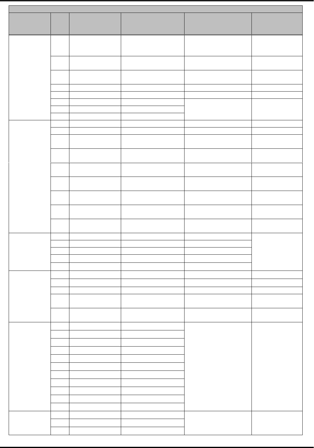
●Assignment of connector pins
Connector Pin
Type
Pin
No.
Pin Name
Signal Direction
(UM04-KO ⇔
external device)
Signal Function
Setting of
unused pins
Power supply
1
SG
-
Grounding
Unconnection
prohibited
20
SG
-
22
SG
-
23
SG
-
28
SG
-
33
SG
-
37
SG
-
51
SG
-
53
SG
-
55
SG
-
57
SG
-
2
VCC
←
Power Supply
(3.3 to 4.2V)
4
VCC
←
6
VCC
←
48
VCC
←
50
VCC
←
Power supply
control
30
PWRKEY
←
Power ON/OFF request
Open
43
SYSRST
←
System reset
Open
UARTserial
interface
41
XCD
→
Carrier detection signal
Open
39
XCI
→
Incoming call indication
signal
Open
35
XCS
→
Permission signal of
sending from this device
Open
32
XRS
←
Request signal of
sending from external
device
Open
31
XER
←
Ready signal from
external device
Open
29
XDR
→
Ready signal from this
device
Open
27
RD
→
Received data
Open
25
SD
←
Sending data
Open
19
DTE1
←
External device serial
communication data
speed configuration
Open
17
DTE2
←
Open
21
DTE3
←
Open
Monitor interface
13
PACKET
→
In packet service
area/Out of packet
service area
Open
11
ANT3
→
Antenna indication 3
Open
9
ANT2
→
Antenna indication 2
Open
7
ANT1
→
Antenna indication 1
Open
40
LEDG
→
For communication
status display
Open
36
LEDR
→
For communication
status display
Open
34
LEDGMS
→
For communication
status display
Open
UIM card
interface
18
SIM_VCC(C1)
→
Power to the UIM card
Unconnection
prohibited
15
SIM_RST(C2)
→
Reset signal
14
SIM_CLK(C3)
→
Clock signal
12
SIM_GND(C5)
-
Ground
10
SIM_DIO(C7)
⇔
Data input/output
Maintenance
interface
3
N.C.
-
Manufacturer
maintenance
Connection
prohibited
16
N.C.
-
26
N.C.
-
38
N.C.
-
42
N.C.
-

Version 1.0
11
Connector Pin
Type
Pin
No.
Pin Name
Signal Direction
(UM04-KO ⇔
external device)
Signal Function
Setting of
unused pins
44
N.C.
-
45
N.C.
-
46
N.C.
-
47
N.C.
-
49
N.C.
-
52
N.C.
-
54
N.C.
-
56
N.C.
-
N.C.
5
N.C.
-
Not used
Connection
prohibited
8
N.C.
-
Not used
Connection
prohibited
24
N.C.
-
Not used
Connection
prohibited
Version 1.0
12
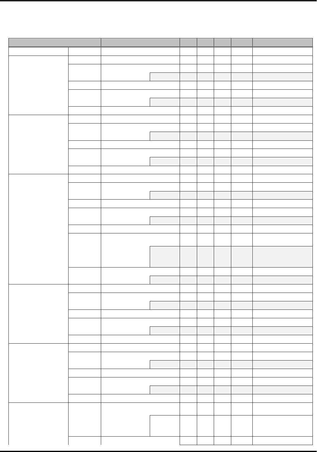
●Electrical characteristics
Item
Pin No.
Min
Typ
Max
Unit
Remarks
Power supply input
VCC
2,4,6,48,50
3.3
3.7
4.2
V
-
Power supply control
PWRKEY
VT+
30
0.77
-
1.44
V
Schmitt trigger
VIH
30
1.44
-
5.25
V
-
ILEAK
-
-
10
μA
-
VT-
30
0.33
-
0.77
V
Schmitt trigger
VIL
30
0
-
0.33
V
-
ILEAK
-
-
-10
μA
-
Hysteresis
30
0.34
-
0.8
V
-
Power supply control
SYSRST
VT+
43
0.7
1.1
1.5
V
Schmitt trigger
VIH
43
1.5
-
5.25
V
-
ILEAK
-
-
10
μA
-
VT-
43
0.25
0.61
0.9
V
Schmitt trigger
VIL
43
0
-
0.25
V
-
ILEAK
-
-
-10
μA
-
Hysteresis
43
0.15
0.49
1
V
-
UARTserial interface
XCD, XCI, XCS, XRS,
XER, XDR, SD, RD
VT+
25,31,32
0.7
1.1
1.5
V
Schmitt trigger
VIH
25,31,32
1.5
-
5.25
V
-
ILEAK
-
-
30
μA
-
VT-
25,31,32
0.25
0.61
0.9
V
Schmitt trigger
VIL
25,31,32
0
-
0.25
V
-
ILEAK
-
-
-2
mA
-
Hysteresis
25,31,32
0.15
0.49
1
V
-
VOH
27,29,35,39,41
-
-
5.25
V
Equivalent to open
circuit imp.
IOH
-
-
-
mA
There is no
definition because
of open drain
output
VOL
27,29,35,39,41
0
-
0.33
V
-
IOL
-
2
-
mA
-
Serial communication data
speed configuration
DTE1, DTE2, DTE3
VT+
17,19,21
0.7
1.1
1.5
V
Schmitt trigger
VIH
17,19,21
1.5
-
5.25
V
-
ILEAK
-
-
10
μA
-
VT-
17,19,21
0.25
0.61
0.9
V
Schmitt trigger
VIL
17,19,21
0
-
0.25
V
-
ILEAK
-
-
-10
μA
-
Hysteresis
17,19,21
0.15
0.49
1
V
-
Monitor interface
ANT1, ANT2, ANT3,
LEDR, LEDG,
LEDGMS, PACKET
VOH
7,9,11,13,34,36,40
-
-
5.25
V
Equivalent to
open circuit imp.
IOH
-
-
-
mA
There is no
definition because
of open drain
output
VOL
7,9,11,13,34,36,40
0
-
0.28
V
-
IOL
-
2
-
mA
-
UIM card interface
SIM_VCC(C1)
SIM_RST(C2)
SIM_CLK(C3)
SIM_DIO(7)
Output
18
2.7
-
3.3
V
Class B
voltage
1.62
-
1.98
V
Class C
VIH
10
C1×0.7
-
C1+0.3
V
Class B/C
VIL
10
-0.3
-
C1×0.2
V
Class B/C
VOH
15
C1×0.8
-
C1
V
Class B/C
IOH
-
-1
-
mA
Class B/C
VOL
15
0
-
C1×0.2
V
Class B/C

Version 1.0
13
Item
Pin No.
Min
Typ
Max
Unit
Remarks
IOL
-
-
2
mA
Class B/C
VOH
10
C1×0.7
-
C1
V
Class B/C
IOH
-
-1
-
mA
Class B/C
VOL
10
0
-
0.4
V
Class B
0
-
0.3
V
Class C
IOL
-
-
1
mA
Class B/C
VOH
14
C1×0.7
-
C1
V
Class B/C
IOH
-
-1
-
mA
Class B/C
VOL
14
0
-
C1×0.2
V
Class B/C
IOL
-
-
2
mA
Class B/C
Version 1.0
14
■BtoB Connector
This flexible connector is same as one used in UM03-KO.
Connector specification
Number of pins
80
Pin pitch
0.5 ㎜
Connection type
Board to Board Connector
Model number
DF12(3.0)-80DS-0.5V(86)
Manufacturer
Hirose Electric CO., LTD.
◆Please use the connector shown in the following table for the external device which connected to this device.
Connector specification
Number of pins
80
Pin pitch
0.5mm
Connection type
Board to Board Connector
Model number
DF12B(3.0)-80DP-0.5V(86)
Manufacturer
Hirose Electric CO., LTD.
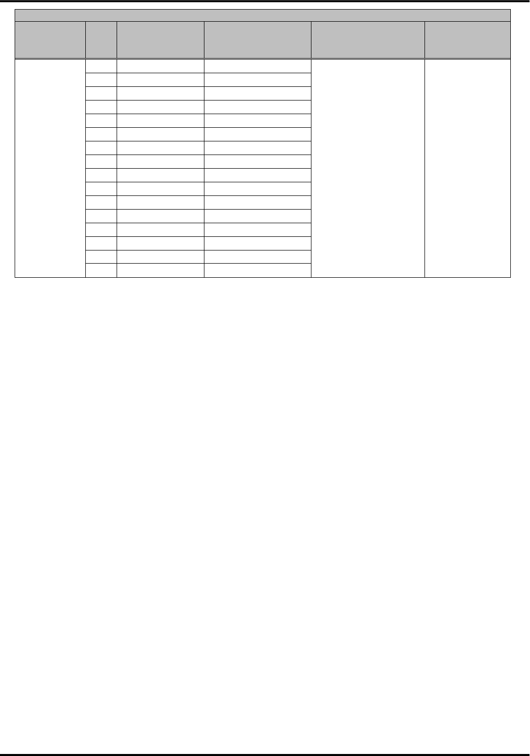
●Assignment of connector pins
Connector Pin
Type
Pin
No.
Pin Name
Signal Direction
(UM04-KO⇔external
device)
Signal Function
Setting of
Unused pins
Power supply
14
SG
-
Grounding
Unconnection
prohibited
18
SG
-
21
SG
-
31
SG
-
34
SG
-
37
SG
-
38
SG
-
39
SG
-
40
SG
-
51
SG
-
41
VCC
←
Power supply
(3.3 to 4.2V)
Unconnection
prohibited
42
VCC
←
43
VCC
←
44
VCC
←
45
VCC
←
46
VCC
←
49
BtoB_DET(SG)
-
BtoB connection
detection signal
Unconnection
prohibited
[Note1]
Power supply
control
5
PWRKEY_ON_n
←
Power ON request
Open
6
PWRKEY_OFF_n
←
Power OFF request
Open
4
SYSRST_n
←
System reset
Open
UARTserial
interface
76
XCD
→
Carrier detection signal
Open
80
XCI
→
Incoming call indication
signal
Open
78
XCS
→
Permission signal of
sending from this device
Open
Version 1.0
15
Connector Pin
Type
Pin
No.
Pin Name
Signal Direction
(UM04-KO⇔external
device)
Signal Function
Setting of
Unused pins
1
XRS
←
Request signal of
sending from external
device
Open [Note2]
3
XER
←
Ready signal from
external device
Open [Note2]
79
XDR
→
Ready signal from this
device
Open
77
RD
→
Received data
Open
2
SD
←
Sending data
Open [Note2]
10
DTE1
←
External device serial
communication data
speed configuration
Depends on
configured value
11
DTE2
←
12
DTE3
←
モニタ
インタフェース
71
ANT1_n
→
Antenna indication 1
Open
72
ANT2_n
→
Antenna indication 2
Open
70
TRX_n
→
Packet communication
status indication
Open
48
LEDG_n
→
Operation status
indication
Open
47
LEDGMS_n
→
Communication status
indication
Open
30
ADL_n
→
Software update status
indication
Open
68
SMS_n
→
Notification of SMS
receiving
Open
67
CBS_ETWS_n
→
Notification of Area
Mail receiving
Open
74
3G/LTE (GSM)
→
Attached network
indication
Open
UIM card
interface
54
SIM_VCC(C1)
→
Power supply
Unconnection
prohibited
52
SIM_RST(C2)
→
Reset Signal
55
SIM_CLK(C3)
→
Clock signal
56
SIM_GND(C5)
-
Grounding
53
SIM_DIO(C7)
⇔
Data input/output
USB interface
20
USB_DPLUS
⇔
Data signal +
Open
19
USB_DMINUS
⇔
Data signal -
Open
23
USB_VBUS
←
USB detection signal
Open
22
USB_H_RDY_n
←
Request of activation
from external device
Pull-down
[Note3]
66
USB_D_RDY_n
→
Request of activation
from this device
Open
Maintenance
interface
17
N.C.
-
Manufacturer
maintenance
Connection
prohibited
25
N.C.
-
58
N.C.
-
59
N.C.
-
60
N.C.
-
61
N.C.
-
62
N.C.
-
63
N.C.
-
64
N.C.
-
65
N.C.
-
73
N.C.
-
N.C.
7
N.C.
-
Not used
Connection
prohibited
8
N.C.
-
9
N.C.
-
Version 1.0
16
Connector Pin
Type
Pin
No.
Pin Name
Signal Direction
(UM04-KO⇔external
device)
Signal Function
Setting of
Unused pins
13
N.C.
-
15
N.C.
-
16
N.C.
-
24
N.C.
-
26
N.C.
-
27
N.C.
-
28
N.C.
-
29
N.C.
-
32
N.C.
-
33
N.C.
-
35
N.C.
-
36
N.C.
-
50
N.C.
-
57
N.C.
-
69
N.C.
-
75
N.C.
-
[Note1] This signal is for the detection of BtoB connector connection. Please connect to SG without fail.
[Note2] The connection of the pull-up resistor is no problem. In case of connecting the pull-up resistor, please use the
power supply for pulling up within +1.8V to +5.25V.
[Note3] Recommended resistor value of the pulling down is 10kΩ to 100kΩ. Direct connection with SG is no problem.
Version 1.0
17
●Electrical characteristics
Current I regards its direction to flow into this device as plus.
Item
Pin No.
Min
Typ
Max
Unit
Remarks
Power supply input
VCC
41,42,43,44,45,46
3.3
3.7
4.2
V
-
Power supply control
PWRKEY_ON_n
VT+
5
0.77
-
1.44
V
Schmitt trigger
VIH
5
1.44
-
5.25
V
-
ILEAK
-
-
10
μA
-
VT-
5
0.33
-
0.77
V
Schmitt trigger
VIL
5
0
-
0.33
V
-
ILEAK
-
-
-10
μA
-
Hysteresis
5
0.34
-
0.8
V
-
Power supply control
PWRKEY_OFF_n
SYSRST_n
VT+
4,6
0.7
1.1
1.5
V
Schmitt trigger
VIH
4,6
1.5
-
5.25
V
-
ILEAK
-
-
10
μA
-
VT-
4,6
0.25
0.61
0.9
V
Schmitt trigger
VIL
4,6
0
-
0.25
V
-
ILEAK
-
-
-10
μA
-
Hysteresis
4,6
0.15
0.49
1
V
-
UARTserial interface
XCD, XCI, XCS, XRS,
XER, XDR, SD, RD
VT+
1,2,3
0.7
1.1
1.5
V
Schmitt trigger
VIH
1,2,3
1.5
-
5.25
V
-
ILEAK
-
-
30
μA
-
VT-
1,2,3
0.25
0.61
0.9
V
Schmitt trigger
VIL
1,2,3
0
-
0.25
V
-
ILEAK
-
-
-2
mA
-
Hysteresis
1,2,3
0.15
0.49
1
V
-
VOH
76,77,78,79,80
-
-
5.25
V
Equivalent to open
circuit imp.
IOH
-
-
-
mA
There is no definition
because of open drain
output
VOL
76,77,78,79,80
0
-
0.33
V
-
IOL
-
2
-
mA
-
Serial communication
data speed configuration
DTE1, DTE2, DTE3
VT+
10,11,12
0.7
1.1
1.5
V
Schmitt trigger
VIH
10,11,12
1.5
-
5.25
V
-
ILEAK
-
-
10
μA
-
VT-
10,11,12
0.25
0.61
0.9
V
Schmitt trigger
VIL
10,11,12
0
-
0.25
V
-
ILEAK
-
-
-10
μA
-
Hysteresis
10,11,12
0.15
0.49
1
V
-
USB interface
USB_H_RDY_n
VT+
22
0.7
1.1
1.5
V
Schmitt trigger
VIH
22
1.5
-
5.25
V
-
ILEAK
-
-
10
μA
-
VT-
22
0.25
0.61
0.9
V
Schmitt trigger
VIL
22
0
-
0.25
V
-
ILEAK
-
-
-10
μA
-
Hysteresis
22
0.15
0.49
1
V
-
USB_D_RDY_n
VOH
66
-
-
5.25
V
Equivalent to open
circuit imp.
IOH
-
-
-
mA
There is no definition
because of open drain
output
VOL
66
0
-
0.33
V
-
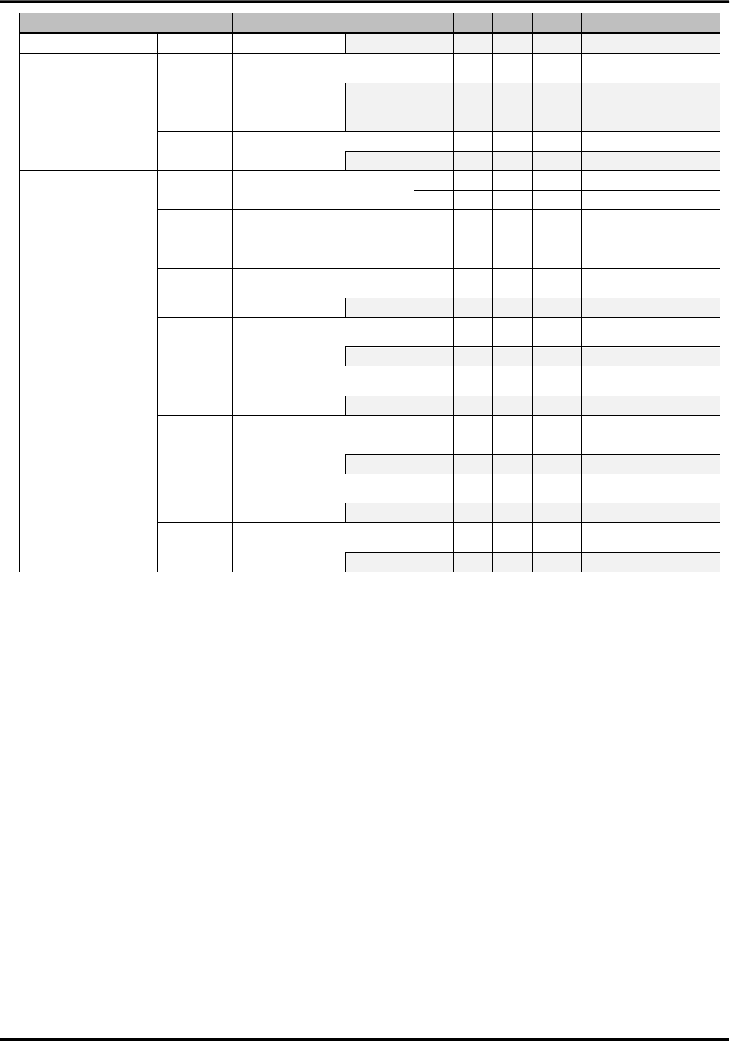
Version 1.0
18
Item
Pin No.
Min
Typ
Max
Unit
Remarks
IOL
-
2
-
mA
-
Monitor interface
ANT1_n, ANT2_n,
TRX_n, LEDG_n,
LEDGMS_n,
SMS_n,ADL_n,
CBS_ETWS_n,
3G/LTE(GSM)
VOH
30,47,48,67,68,69,
-
-
5.25
V
Equivalent to open
circuit imp.
70,71,72,74
IOH
-
-
-
mA
There is no definition
because of open drain
output
VOL
30,47,48,67,68,
0
-
0.28
V
-
70,71,72,74
IOL
-
2
-
mA
-
UIM card interface
SIM_VCC(C1)
SIM_RST(C2)
SIM_CLK(C3)
SIM_DIO(7)
Output
54
2.7
-
3.3
V
Class B
voltage
1.62
-
1.98
V
Class C
VIH
53
C1×
0.7
-
C1+
0.3
V
Class B/C
VIL
-0.3
-
C1×
0.2
V
Class B/C
VOH
52
C1×
0.8
-
C1
V
Class B/C
IOH
-
-1
-
mA
Class B/C
VOL
52
0
-
C1×
0.2
V
Class B/C
IOL
-
-
2
mA
Class B/C
VOH
53
C1×
0.7
-
C1
V
Class B/C
IOH
-
-1
-
mA
Class B/C
VOL
53
0
-
0.4
V
Class B
0
-
0.3
V
Class C
IOL
-
-
1
mA
Class B/C
VOH
55
C1×
0.7
-
C1
V
Class B/C
IOH
-
-1
-
mA
Class B/C
VOL
55
0
-
C1×
0.2
V
Class B/C
IOL
-
-
2
mA
Class B/C
Version 1.0
19
2.Power supply
(1) Recommended specification for the external power supply
Item
Specification
Voltage range
DC+3.3V to +4.2V (Load condition: Steady supply
in 0.1mA to 1,500mA)
Ripple
50mVp-p (0Hz to 2.5GHz) or less
Rating current
1,500mA or more
Inrush current
2A (within 100μs) or less
(2) Power supply input specification
Pin name
Min
Typ
Max
Unit
Remarks
VCC
+3.3
+3.7
+4.2
V
-
(3) Transient specification of the power supply voltage rising
Pin name
Min
Typ
Max
Unit
Remarks
VCC
-
-
50
msec
Refer to the following figure for
waveform.
●Transient waveform of power supply voltage rising
T[msec]
50msec
Steady supply
4.2
3.7
3.3
VCC[V]
0
Version 1.0
20
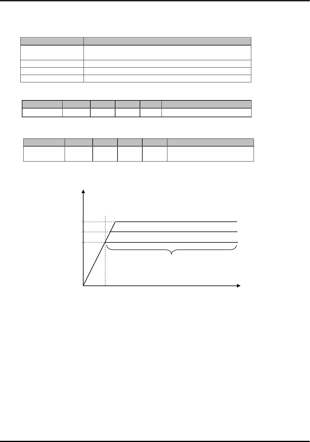
■Power supply control
(1) Power supply control
●Start/Stop flow of this device
●Power supply control
Item
Process
Remarks
Automatic start
・This device automatically starts by being
supplied
・LEDG_n becomes SG by start
Start
・To start this device in stop state, please
make PWRKEY_ON_n SG or power
supply stop with the interval more than
three seconds, and then start by applying
power supply again.
Stop
・This device stops by making
PWRKEY_OFF_n pin SG or carrying out
AT*DPWROFF.
・When this device is in stop state by stop
of power supply, LEDG_n becomes
OPEN.
Under starting process
In operation state
PWRKEY_OFF_n to SG
AT*DPWROFF
This device stop state
PPWRKEY_ON_n to SG
Power supply stop
Power supply start
Automatic start
Process to stop
Process to start
Version 1.0
21
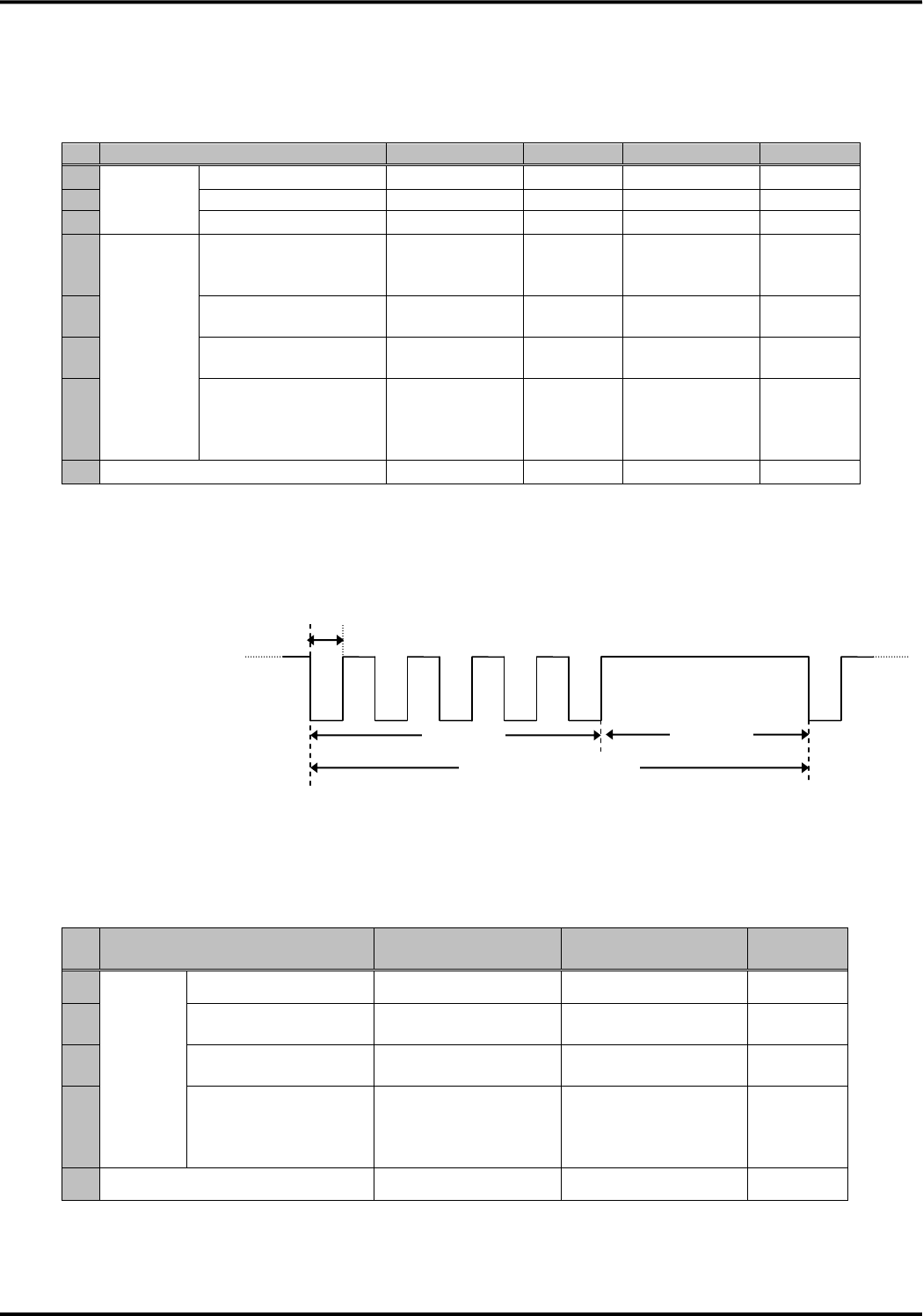
(2) Pin behavior and AC characteristics
●This device operation for the PWRKEY_ON_n input status
Because it causes the malfunction, please input pulses more than specified time. It is recognized as a
demand only at the time of state change from OPEN to SG.
Pin state
Process of this device
OPEN→SG→OPEN
Start request
(It is recognized as a demand only at the time of state change from
OPEN to SG)
●AC characteristics of PWRKEY_ON_n pin
Item
Min
Typ
Max
Unit
Remarks
PWRKEY_ON_n
TPWRKEY_ON
1
-
-
msec
-
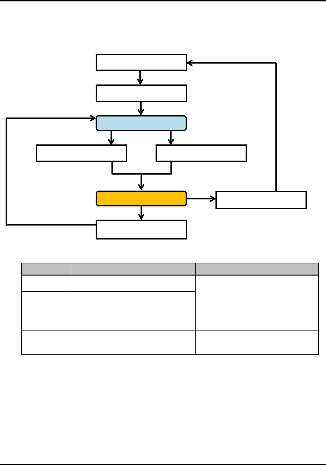
●This device operation for the PWRKEY_OFF_n pin status
Because it causes the malfunction, please input pulses more than specified time. It is recognized as a
demand when SG state continues more than 500msec.
Pin state
Process of this device
OPEN→SG→OPEN
Stop request
(It is recognized as a demand when SG state continues SG more than
500msec.)
●AC characteristics of PWRKEY_OFF_n pin
Item
Min
Typ
Max
Unit
Remarks
PWRKEY_OFF_n
TPWRKEY_OFF
500
-
-
msec
-
PWRKEY_ON_n
VIL
VIL
OPEN
TPWRKEY_ON
SG
TPWRKEY_OFF
PWRKEY_OFF_n
VIL
VIL
OPEN
SG
Version 1.0
22
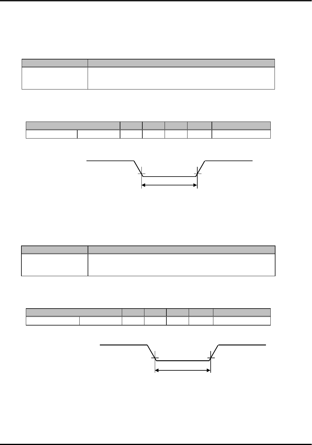
●This device operation for the SYSRST_n pin status
Because it causes the malfunction, please input pulses more than specified time.
Pin state
Process of this device
OPEN→SG→OPEN
Hardware reset
(During SG state, hardware reset occurs)
●AC characteristics of SYSRST_n pin
Item
Min
Typ
Max
Unit
Remarks
SYSRST_n
TSYSRST
50
-
-
msec
-
SYSRST_n
VIL
TSYSRST
VIL
OPEN
SG
Version 1.0
23
(3) Sequence
Start and stop sequences are shown below.
◆Start method (two types) ◆Stop method (two types)
・Automatic start ・Stop by PWRKEY_OFF_n pin
・Start by PWRKEY_ON_n pin ・Stop by AT command
●Automatic start sequence (XER-SG state)
・Though this device starts automatically in case of XER-OPEN, the XCS and XDR line remain OPEN.
VCC
OPEN
Max 5 sec
Power supply
LEDG_n
XCS
XDR
OPEN
SG
OPEN
SG
OPEN
SG
PWRKEY_ON_n
OPEN
SG
OPEN
SG
PWRKEY_OFF_n
This device start
Stop demand recognition
is impossible
Stop demand recognition is possible
Start demand recognition is impossible
Max 20 sec
Reading time of UIM card
AT command is controllable
Version 1.0
24
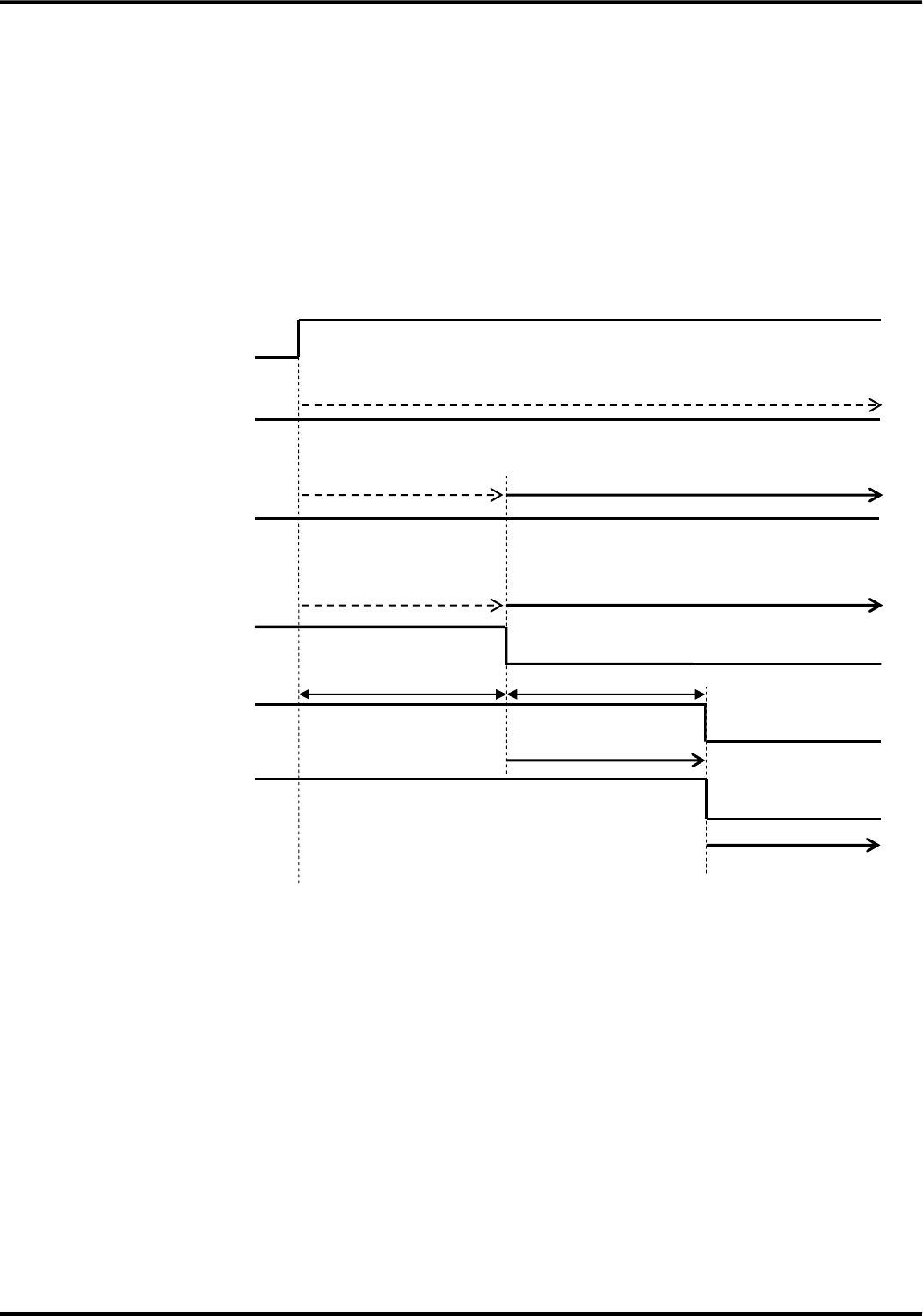
●Start sequence by PWRKEY_ON_n pin (XER-SG state)
・In case of XER-HIGH, the XCS and XDR line remain OPEN.
・Please use this sequence for the start in the VCC supply state after the stop by PWRKEY_OFF_n pin or
the AT command.
・Because this device automatically starts regardless of the behavior of PWRKEY_ON_n pin, the start
demand by PWRKEY_ON_n pin is not recognized at the time of the automatic start. Before start by
PWRKEY_ON_n, please make sure to change PWRKEY_OFF_n to OPEN. When start process is carried
out by PWRKEY_OFF_n while PWRKEY_ON_n is SG, this device detects that PWRKEY_OFF_n is SG
after start process completed and it stops.
VCC
Stop demand recognition is possible
1 msec
Recognize start
Power supply
LEDG_n
XCS
XDR
OPEN
SG
OPEN
SG
OPEN
SG
This device start
Reading time of UIM card
PWRKEY_ON_n
OPEN
SG
PWRKEY_OFF_n
OPEN
SG
Stop demand recognition
is impossible
Max 5 sec
Max 20 sec
AT command is controllable
Version 1.0
25
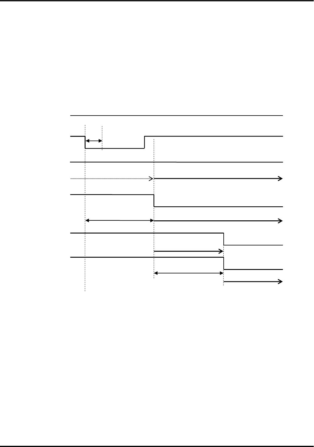
●Stop sequence by PWRKEY_OFF_n pin
・After PWRKEY_OFF_n pin SG is carried out for 500 ms, there is no problem even if it is returned to OPEN
in any timing. Please return it to OPEN before the next start. When start process is carried out while
PWRKEY_OFF_n is SG, this device detects that PWRKEY_OFF_n is SG after start process completed and it
stops.
500 msec
During stop process of this device (within TBD sec)
OPEN
SG
Power supply
LEDG_n
XCS
XDR
VCC
OPEN
SG
OPEN
SG
This device stop
PWRKEY_OF
F_n
OPEN
SG
Recognize a stop demand
PWRKEY_ON
_n
OPEN
SG
Start demand recognition is impossible
Stop of VCC supply is possible
Within 2.5 sec
Version 1.0
26
(4) Connection example
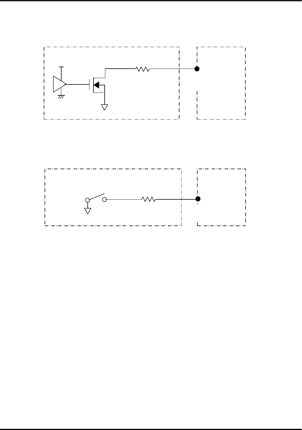
●PWRKEY_ON_n pin, PWRKEY_OFF_n pin, SYSRST_n pin
①Connection example with IC
※ R is a dumping resistor. Please design it to adapt to the circuitry in the external device.
②Connection example with switch
※ R is a dumping resistor. Please design it to adapt to the circuitry in the external device.
This device
↑
Input pin
R
(Open drain output)
IC
VCC1
External device
This device
↑
Input pin
External device
R

Version 1.0
27
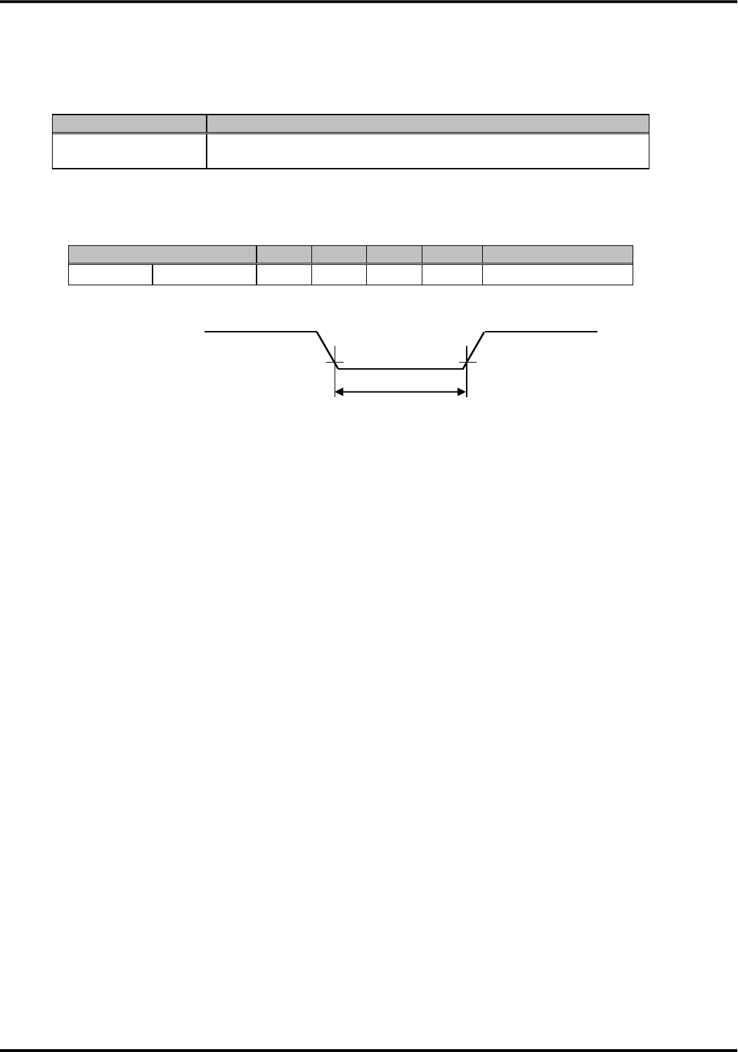
■System reset
The specification of system reset signal is shown below.
◆AC characteristic of SYSRST pin
Item
Min
Typ
Max
Unit
Remarks
SYSRST_n
TSYSRST
1.0
-
-
ms
-
・Please do not usually use SYSRST pin.
・But because the system reset does not carry out the normal stop process and internal data saving of this
device, it may cause the internal data failure and this device may not start normally.
Version 1.0
28
3.UART interface
The specification of the UART is shown below
Item
Specification
Signal line
SD, RD, XER, XDR, XRS, XCS, XCD, XCI
Communication data
speed [bps]
1200/2400/4800/9600/19200/38400/57600/115200/230400/460800
Configuration method
of communication data
speed
External pins (DTE1, DTE2, DTE3), AT command
Communication format
Start:1bit, Stop:1bit, Data:8bit, Parity:none
Sending/Receiving
control
hardware flow control, software flow control, and without flow control
Detection of escape
+++ (guard time is specified)
Detection of break
None
Baud rate deviation
Sending:2% or less
Receiving:2% or less
■Configuration of serial communication data speed by AT command
Only when the configuration of serial communication data speed by DTE1, DTE2 and DTE3 is 19200 [bps], the
configuration by AT command can be used.
●The serial communication data speed configured by AT+IPR
Serial communication data speed[bps]
Remarks
1
1200
-
2
2400
-
3
4800
-
4
9600
-
5
19200
Initial value
6
38400
-
7
57600
-
8
115200
-
9
230400
-
10
460800
-
Version 1.0
29
■Connection example
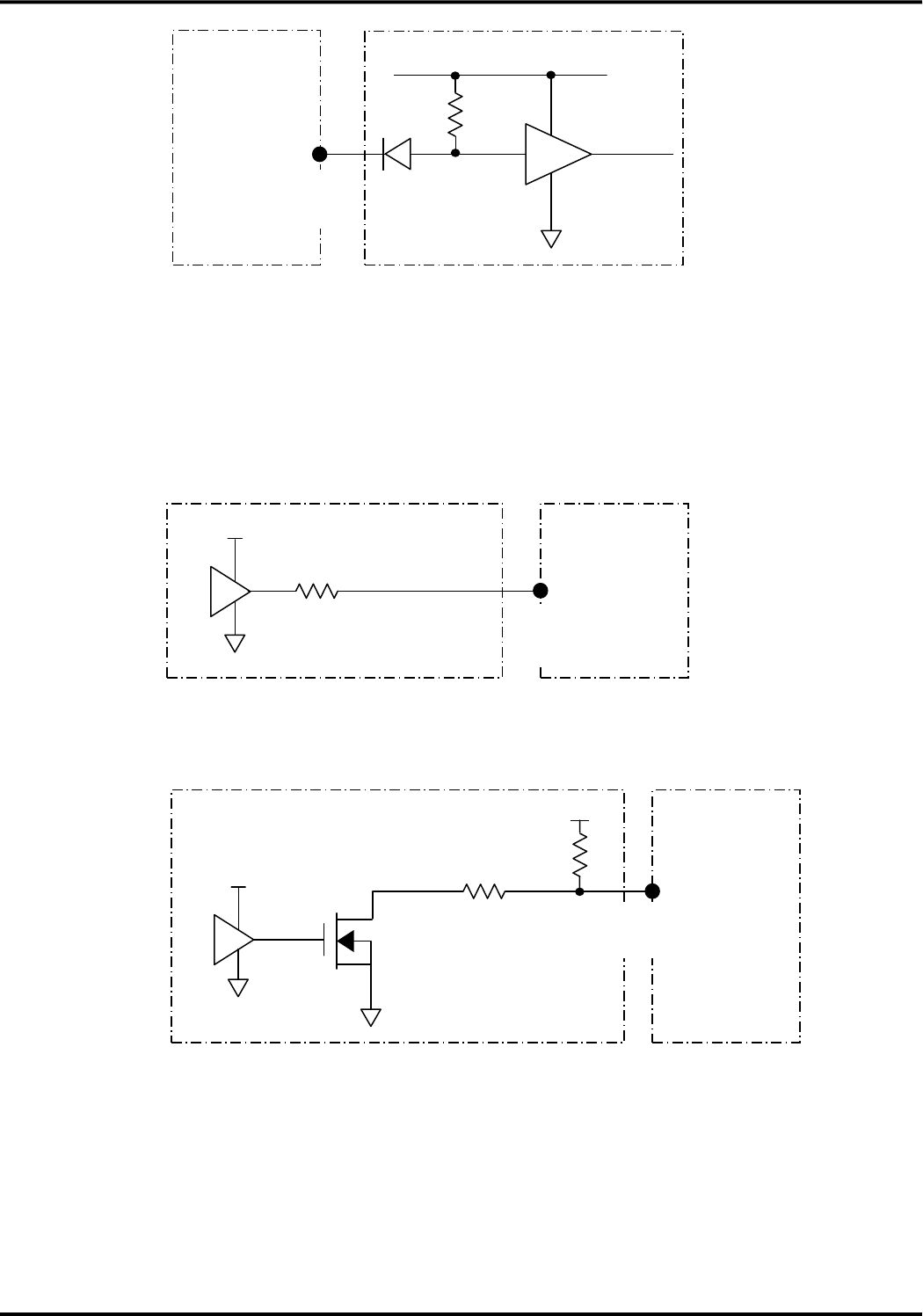
●Connection to the flexible connector
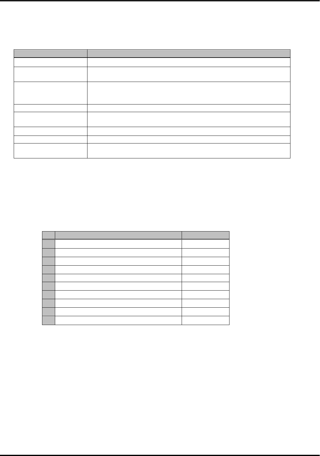
(1) Connection example to the UART serial interface output pin
The UART serial interface output pins are the open drain output. At the time of the stop, it becomes high
impedance state. Unused pins should be OPEN.
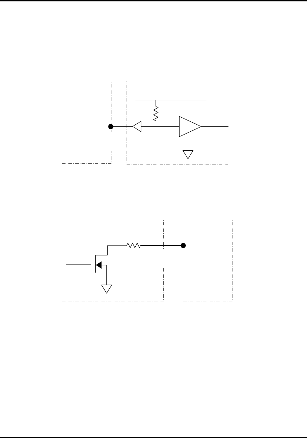
(2) Connection example to the UART serial interface input pin
When this device is power off, it becomes high impedance state.
This device
10kΩ
↑
Output pin
Max5.25V
External device
External device
This device
↑
Input pin
47Ω
(Open drain output)
Version 1.0
30
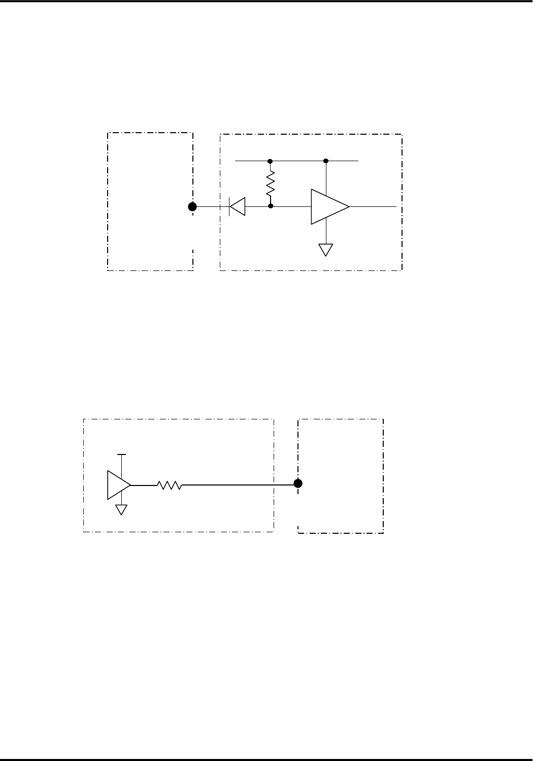
●Connection to BtoB connector
(1) Connection example to the UART serial interface output pin (XCD、XCI、XCS、XDR、RD)
The UART serial interface output pins are the open drain output. At the time of the stop, it becomes high
impedance state. Unused pins should be OPEN.
[Note] R is pull-up resistor. Please design it to adapt to the circuitry in the external device.
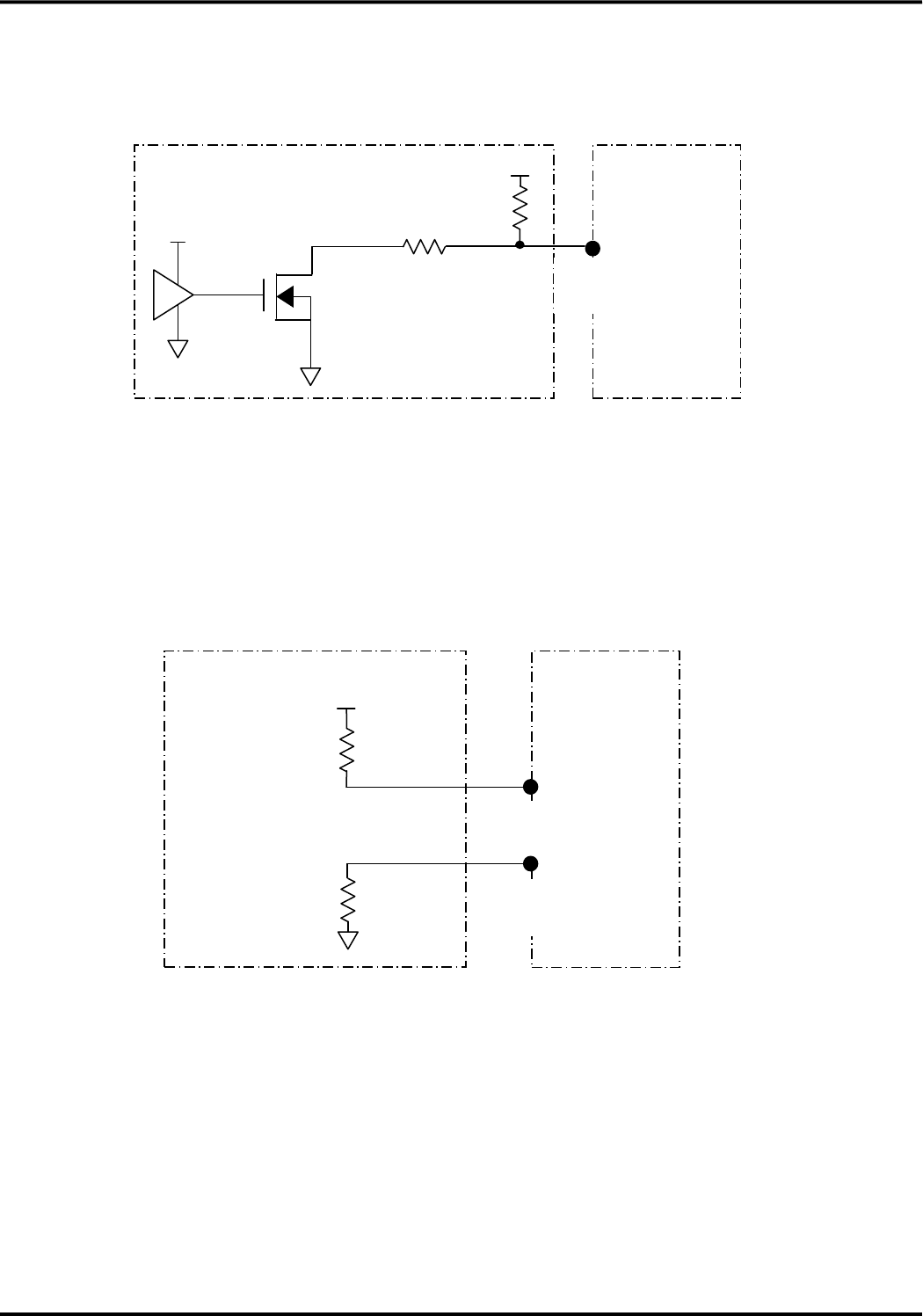
(2) Direct Connection example to the UART serial interface input pins (XRS, XER, SD, DTE1, DTE2, DTE3)
The input pins are the Schmitt trigger input with tolerant of 5V
●Direct connection example to the UART serial interface input pins
[Note] R is pull-up resistor. Please design it to adapt to the circuitry in the external device.
This device
↑
Output pin
R
External device
+1.8V~+5V
R
This device
↑
Input pin
IC
External device
Version 1.0
31
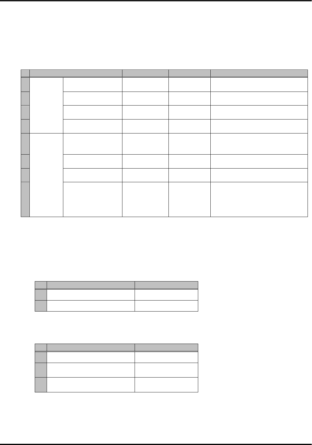
●Open drain connection example to the UART serial interface input pins
Please input the open drain output when the external device which can not meet DC characteristic is
connected.
[Note] R1 is pull-up resistor and R2 is dumping resistor. Please design it to adapt to the circuitry in the
external device.
●Connection example to DTE1、DTE2、DTE3 input pins
When fixed serial communication data speed is used, please fix the level by pull-up or pull-down
depending on configuration value.
[Note] R1 is pull-up resistor and R2 is pull-down resistor. Please design it to adapt to the circuitry in the
external device.
[Requirement of SD pin and RD pin]
(1) Requirement of SD pin (input)
①When the external device which is connected to SD pin can not meet DC characteristic, it is necessary
to be connected by the open drain output. Dull of wave pattern caused by connection of the open drain
output may cause data communication failure. Therefore, requirement for the input waveform for the
connection of the open drain output is specified.
R2
+1.8V~+5V
R1
This device
↑
Input pin
(Open drain output)
IC
VCC1
External device
R1
+1.8V~+5V
R2
Pull-up
This device
↑
Input pin
Pull-down
↑
Input pin
External device
Version 1.0
32
②For the requirement for SD pin input waveforms, the ratio per one bit of data which is measured in
voltage level of SG interval [A] and OPEN interval [B] should be adjusted within from 50:50 to 56:44.
・This requirement is applied for the waveform that was measured at the most close point to the main
connector.
・The slope of the rising wave pattern depends on the circuitry of the external device. In case that the
dull of the wave pattern is big and the ratio of SG is wider, for example, please adjust it so that the dull
of the wave pattern becomes small to reduce the pull-up resistor value.
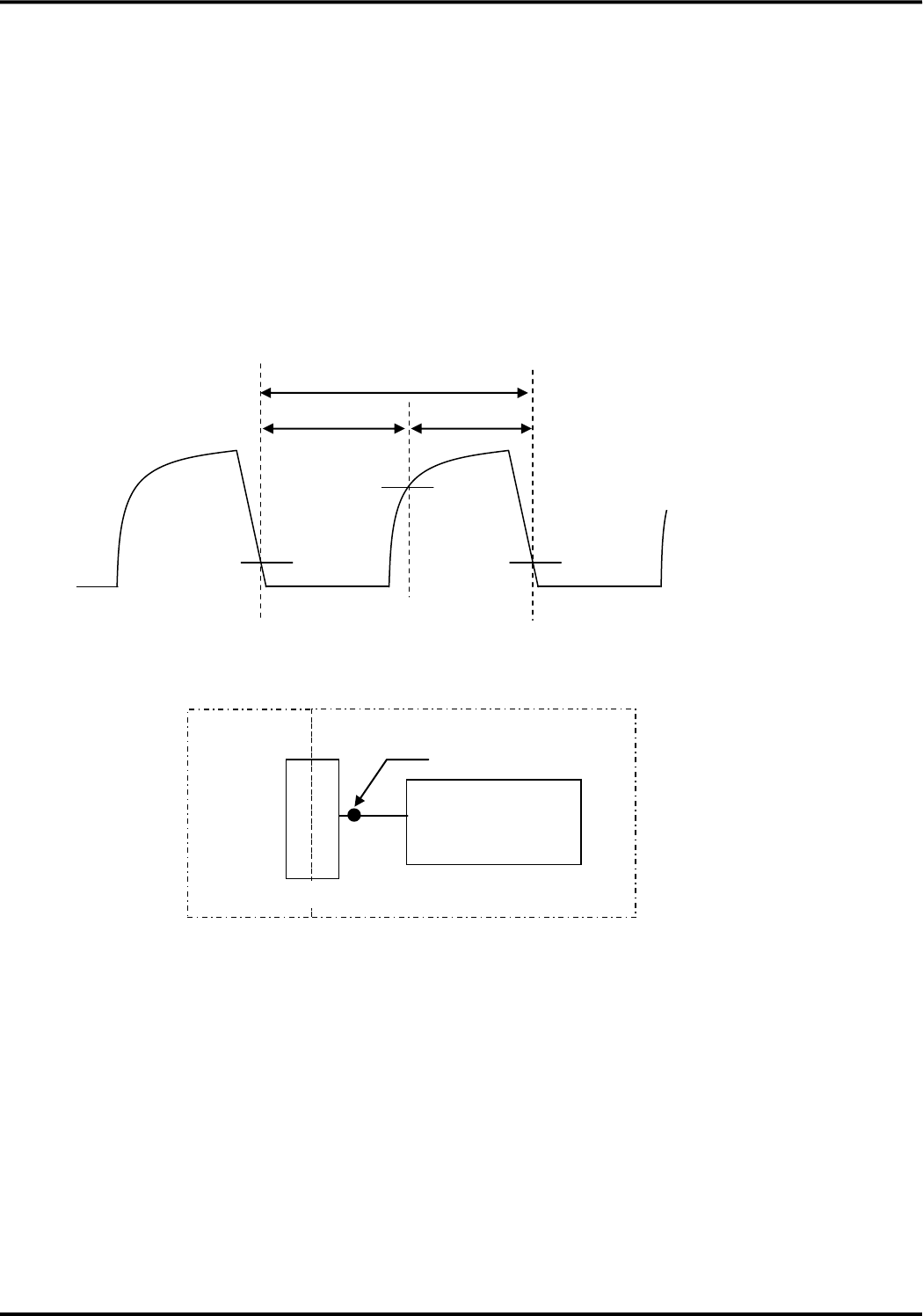
●SD pin (input) wave pattern
●Waveform measurement point of UART serial receiving data (SD pin)
(2)Requirement of RD pin (output)
①The RD pin is the open drain output.
②Dull of rising wave pattern may cause any failure. Please confirm it each external devices to be
connected. In case that the dull of the wave pattern is big, for example, please adjust it in external
device so that the dull of the wave pattern becomes small to reduce the pull-up resistor value.
SD pin
Vt+(Max)1.29V
【A】
【B】
Vt-(Max)0.67V
Vt-(Max)0.67V
Assume this section 100
The ratio of 【A】 and 【B】
Within from 50:50 to 56:44
Vt+:The OPEN level threshold voltage of
this device
Vt-:The SG level threshold voltage of this
device
This device
External device
Main connector
Circuit
Measurement point
Version 1.0
33
4.USB interface
The USB interface of this device is based on USB 2.0 specification. The transmission and reception of data is
possible as a USB device. You can use it for the control by the AT command. The connection with the USB host
is disconnected when you make reboot (power off / on, reset by AT*DHWRST).
Item
Specification
Communication
standard
Conformity USB2.0 (Device)
Communication
speed
FULL SPEED (12Mbit/s), 、HIGH SPEED (480Mbit/s)
Signals
USB_DPLUS, USB_DMINUS, USB_VBUS, USB_H_RDY_n,
USB_D_RDY_n
Virtual COM port
Port1 : Modem control
Port2 : Network card control
■Connection example
(1) USB interface pin (USB_DPLUS, USB_DMINUS, USB_VBUS)
●Connection example to the external device
[Note] USB_VBUS does not mean power supply of 5V from a host, and it mean a USB host connection state.
(2)USB_D_RDY_n output pin
This output pin is the open drain output.
At the time of the stop of this device, it becomes the high impedance state. In case of unused condition, set a
pin as OPEN.
●Connection example to USB_D_RDY_n output pin
This device
USB_DPLUS
USB_DMINUS
USB_VBUS
SG
USB host
External device
Version 1.0
34
[Note] R is pull-up resistor. Please design it to adapt to the circuitry in the external device.
(3)USB_H_RDY_n input pin
The input composes it of Schmidt trigger of 5V tolerant.
When you connect the external device which cannot meet DC characteristics, it is necessary to input at this
device by the output of the open drain.
●Direct connection example to USB_H_RDY_n input pin
[Note] R is dumping resistor. Please design it to adapt to the circuitry in the external device.
●Open drain connection example to USB_H_RDY_n input pin
[Note] R1 is pull-up resistor and R2 is dumping resistor. Please design it to adapt to the circuitry in the
external device.
This device
R
↑
Output pin
External device
+1.8V~+5V
R
This device
↑
Input pin
IC
External device
+1.8V~+5V
R1
R2
This device
↑
Input pin
(Open drain output)
External device
IC
VCC1
Version 1.0
35
5.Monitor interface
■Antenna indication
●Antenna indication specification
State
ANT1_n
ANT2_n
Remarks
1
In
operation
Out of service
OPEN
OPEN
Result code “0” (out of service) for
the AT command “AT*DANTE”.
2
Antenna one bar
SG
OPEN
Result code “1” (one bar) for the AT
command “AT*DANTE”.
3
Antenna two bars
OPEN
SG
Result code “2” (two bars) for the AT
command “AT*DANTE”.
4
Antenna three bars
SG
SG
Result code “3” (three bars) for the
AT command “AT*DANTE”.
5
During
software
update
During download
Depends on
receiving signal
level
Depends on
receiving
signal level
-
6
During rewriting
(SW update mode 3)
SG
SG
Equals to the state of antenna three
bars
7
During reboot
(SW update mode 3)
OPEN
OPEN
-
8
During the update
completion
notification
transmitting
(SW update mode 3)
Depends on
receiving signal
level
Depends on
receiving
signal level
-
※ Refer to “Software update” about the function of software update.
■Attached network indication
3G/LTE (GSM) signal indicates the attached network.
(1)LTE mode
●Attached network indication only in LTE mode (only in Japan)
Service status
3G/LTE(GSM)
1
In service of LTE
SG
2
Out of service of LTE
OPEN
(2)Roaming mode
●Attached network indication in roaming mode (out of Japan)
Service status
3G/LTE (GSM)
1
In service of W-CDMA
OPEN
2
Out of service of W-CDMA
and in service of GSM
SG
3
Out of service of W-CDMA
and out of service of GSM
OPEN
Version 1.0
36
■Communication state indication
Communication state is indicated based on the combination of TRX_n, LEDG_n and LEDGMS_n.
●Communication state indication specification
State
TRX_n
LEDG_n
LEDGMS_n
Remarks
1
In
operation
During stand-by
OPEN
SG
OPEN
-
2
During communication
SG
SG
OPEN
3
During incoming
OPEN
SG
SG⇔OPEN
[Note1]
4
During
software
update
During download
Depends on
communication
state
SG
Depends on
communication
state
-
5
During rewriting
(SW update mode 3)
OPEN
SG
OPEN
-
6
During reboot
(SW update mode 3)
OPEN
OPEN
OPEN
-
7
During the update
completion notification
transmitting
(SW update mode 3)
Depends on
communication
state
SG
Depends on
communication
state
-
8
Stop state of this device
OPEN
OPEN
OPEN
-
[Note1] Waveform of LEDGMS_n is shown below during incoming.
●Waveform of LEDGMS_n signal during incoming
■Software update state indication
Software update state is indicated by ADL_n signal.
●Software update state indication specification
State
ADL_n
(NW reservation type)
ADL_n
(AT command type)
Remarks
1
During
software
update
During download
OPEN
SG
-
2
During rewriting
(SW update mode 3)
SG
SG
-
3
During reboot
(SW update mode 3)
OPEN
OPEN
-
4
During the update
completion notification
transmitting
(SW update mode 3)
SG
SG
-
5
During other than software update
OPEN
OPEN
-
OPEN
SG
0.2±0.01[s]
1.8±0.01[s]
1.2±0.01[s]
1cycle:3.0±0.01[s]
LEDGMS_n
Version 1.0
37
■SMS receiving indication
The receiving of SMS is indicated by SMS_n.
●SMS receiving indication specification
State
SMS_n
Remarks
1
Receiving SMS
OPEN→SG→OPEN
-
2
Other than SMS receiving
OPEN
-
●Waveform of SMS_n when a SMS is received
■Area Mail receiving indication
The receiving of Area Mail is indicated by CBS_ETWS_n.
●Area Mail receiving indication specification
State
CBS_ETWS_n
Remarks
1
Receiving Area Mail
OPEN→SG→OPEN
-
2
Other than Area Mail receiving
OPEN
-
●Waveform of CBS_ETWS_n when an Area Mail is received
■Connection example
The monitor interface of this device is the open drain output.
●A connection example of the external LED lamp to monitor interface
At the time of the stop of this device, it becomes the high impedance state.
※R is a pull-up resistor. Please assume it a value to adapt to a circuitry of the external device
OPEN
SG
90[ms] or more
CBS_ETWS_n
This device
R
↑
Output pin
External device
OPEN
SG
90[ms] or more
SMS_n
Version 1.0
38
6.UIM card interface
This device is equipped with UIM card interface that meets the 3GPP TS31series specifications.
UIM card is the IC card which can record the information such as phone numbers and inserts it in a card socket of
the external device to connect to this device. Please do not perform take out it, placing it in the power on state to
prevent data damage and UIM card damage.
(1) Signal
●Pin assignment of UIM card ●Pin names of UIM interface
Pin No.
Pin name
1
C1
UIM_VCC(C1)
2
C2
UIM_RST(C2)
3
C3
UIM_CLK(C3)
4
C4
N.C.
5
C5
UIM_GND(C5)
6
C6
N.C.
7
C7
UIM_DIO(C7)
8
C8
N.C.
(2) Electrical characteristic
●DC characteristic
Pin name
Item
Min
Typ
Max
Unit
Remarks
UIM_VCC(C1)
VCC
2.7
-
3.3
V
Class B
1.62
-
1.98
V
Class C
UIM_RST(C2)
VOH
C1×0.8
-
C1
V
Class B/C
IOH
-
-4
-
mA
Class B/C
VOL
0
-
C1×0.2
V
Class B/C
IOL
-
3.9
-
mA
Class B/C
UIM_CLK(C3)
VOH
C1×0.7
-
C1
V
Class B/C
IOH
-
-4
-
mA
Class B/C
VOL
0
-
C1×0.2
V
Class B/C
IOL
-
3.9
-
mA
Class B/C
UIM_DIO(C7)
VIH
C1×0.7
-
C1+0.3
V
Class B/C
VIL
-0.3
-
C1×0.2
V
Class B/C
VOH
C1×0.7
-
C1
V
Class B/C
IOH
-
-4
-
mA
Class B/C
VOL
0
-
C1×0.4
V
Class B
0
-
0.3
V
Class C
IOL
-
-
1
mA
Class B/C
●AC characteristic
Pin name
Item
Min
Typ
Max
Unit
Remarks
UIM_RST(C2)
TR/TF
-
-
400
μs
-
UIM_CLK(C3)
TR/TF
-
-
50
ns
-
UIM_DIO(C7)
TR/TF
-
-
1.0
μs
-
C1
C2
C3
C4
C5
C6
C7
C8
Version 1.0
39
(3) Connection method
For an output signal from this device, please be connected directly with a card socket to comply DC and AC
characteristics. If its connection is not direct, please care for the delay of signal timing and loss of signal level
●The recommended equivalent circuit for UIM card interface
(4) Recommended card socket
Please use the following recommended card socket.
●Recommended card socket
Size
Model
Manufacturer
Remarks
Standard
SF7W006S1AE1000
Japan Aviation Electronics Industry
Hinge type
Mini
SF15W006S4BR2000
Japan Aviation Electronics Industry
Hinge type
(5) PIN code
In this device, only PIN1 code is used for the password of the DOCOMO UIM card.
●About PIN1 code
The PIN1 code is four digits to eight digits of passwords to input to prevent the unauthorized use of the
terminal by the third party.
It comes to be able to use service using LTE networks such as packet communication, SMS by
inputting PIN1 code.
●Input of PIN1 code
Input of the PIN1 code is necessary when PIN1 code becomes effective. At the time of the subscription,
the PIN1 code is set for invalidity.
●Change of PIN1 code
The PIN1 code is set to “0000” at the time of the subscription. You can change the code when necessary.
Please note that three consecutive failed attempts to enter the PIN1 code will automatically lock the code
entry. Please do not forget the set PIN1 code by writing it down and saving it in a secure location
ModemchipLSI
UIM
card
I/F
C1
C2
C3
C5
C7
Power supply part
UIMcardI/F
C1
C2
C3
C5
C7
C4
C6
C8
UIM card
socket
Not in use
Internal of this device
Version 1.0
40
●About PIN1 unlock code
The PIN1 unlock code is used to clear the locked state of the PIN1 code. This code will be provided to
the customer at the time of the subscription. Entering the eight digits PIN1 unlock code clears the locked
state. Note that ten consecutive failed attempts to enter the PIN1 unlock code will automatically lock the
code entry. If you forget the PIN1 unlock code or when the PIN1 code lock can not be cleared, please
contact the customer service.
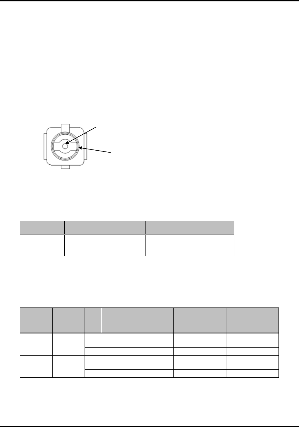
7.RF connector (Main/Sub)
This device is equipped with RF connectors to connect the antenna.
■Used connector
●A model name and the manufacturer name of the RF connector are shown below
RF connector
(This device side)
RF connector [Note1]
(External device side)
Model name
U.FL-R-SMT
U.FL-LP-040
U.FL-LP-066
Manufacturer
Hirose Electric CO., LTD
Hirose Electric CO., LTD
[Note1] Confirm the details with the manufacturer, as the part number will be different depending on the
diameter of the used cable.
■Pin assignment
●Pin assignment
Signal
No.
Pin
name
Description
Signal Direction
(This device ⇔
Antenna)
Remarks
TRX
connector
(Main)
Transmit
and
receive
1
TRX
Transmit and
receive signal
⇔
2GHz/800MHz
RF signals
2
SG
Grounding
-
-
TRX
connector
(Sub)
Receive
1
TRX
Receive signal
⇔
2GHz/800MHz
RF signals
2
SG
Grounding
-
-
Pin1(Signal pin)
Pin2 (SG)
Version 1.0
41
8.External antenna
・The external antenna (optional product) of DOCOMO can be used as the external antenna to be connected to
this device.
・Plural antennas, which are main antenna (for transmit and receive) and sub antenna (for receive), can be
connected.
・About the selection of use of the plural or single antenna, it can be configured by the command
“AT*KMIMO” which is the AT command to select MIMO receiving or not MIMO receiving.
・If “not MIMO receiving” is selected, this device can be in operation with single antenna. In that case, please
connect the external antenna to main antenna connector.
●External antennas of the optional products (Sale product particularly) of DOCOMO
Name
Connector type
Remarks
1
Roof-top antenna for
FOMA adaptor 02
SMA-P
Dual band (2 GHz/800 MHz) antenna
Supplied with an antenna cable (about 5.5 meters long)
2
Simple antenna for
FOMA adaptor
SMA-P
Dual band (2 GHz/800 MHz) antenna
Supplied with an antenna cable (about 5.0 meters long)
3
Compact water-proof
antenna for FOMA
adaptor
SMA-P
Dual band (2 GHz/800 MHz) antenna
Supplied with an antenna cable (about 2.5 meters long)
The connector adaptation methods (U.FL to SMA) for connecting this device to the antenna recommended in the
above list are shown below, with examples of adaptor types.
As the method of connector adaptation, you can use either an adaptor cable or a combination of an adaptor
connector and an RF cable. Please refer to the manufacturer for the specification of cable and connector.
[Adaptor cable]
This adaptor cable is used to converts RF connector (U.FL female) into a SMA-male.
Model number
Manufacturer
Type
Remarks
HRMJ-U.FL-066N1-A-100RS
Hirose Electric CO., LTD
U.FL female to
SMA female
Cable length 100mm
[RF cable and adaptor connector]
●RF cable
Model number
Manufacturer
Type
Remarks
U.FL-2LP-04K2T-A-(80)
Hirose Electric CO., LTD
U.FL female to
U.FL female
Cable length 80mm
Cable color black
●Adaptor connector
Model number
Manufacturer
Type
Remarks
HRMJ-U.FLJ-PC-1
Hirose Electric CO., LTD
U.FL male to
SMA female
For direct connection
to the circuit board.

Version 1.0
42
Precautions for connecting to the external device
Precaution for design of the external device
The external device must be adequately designed to provide sufficient heat dissipation so that the internal
temperature of the external device will not exceed the operating environment temperature range specified for this
device (+60°C) when this device is installed in the external device.
In addition, the external device must be adequately designed to provide sufficient heat dissipation so that the
surface temperature of the enclosure of this device will not exceed +85°C as this device may generate excess heat
depending on the communication condition.
Precautions for connecting to the external device
Precautions for design of the external device
Version 1.0
43
Recommended installation method
■In case of using the flexible connector
In case of using the flexible connector, this device can be used only in Japan.
■In case of using the BtoB connector
BtoB connector for connection to external equipment to is the board to board connector, please use a spacer of
the height same as the stacking height of the board to board connector (3mm).
In case of using the BtoB connector, this device can be used both in Japan and outside of Japan.
Recommended installation method
Screw
External device PCB
・There not being unnecessary radiation in receive frequency band.
・Shields the sensitive circuit as measure to protect from RF power.
・Use a conductive material. (e.g. PCB, metal chassis, etc.)
for the mounting surface of the external device to enable sufficient heat transfer.
・Do not short-circuit with a ground of the external device side.
Flexible cable
・Low DC resistance
RF cable
Heat dissipationsheet
External device PCB
・There not being unnecessary radiation in receive frequency band.
・Shields the sensitive circuit as measure to protect from RF power.
・Use a conductive material. (e.g. PCB, metal chassis, etc.)
for the mounting surface of the external device to enable sufficient heat transfer.
・Do not short-circuit with a ground of the external device side.
M2 hex nut
Metal spacer
Outside diameter:
φ4, L=3 ㎜
This device
BtoB connector
Stancking height 3mm
Graphite sheet
M2 W sems screw
M2 hex nut
This device
Heat dissipationsheet
Graphite sheet
RF cable
M2 W sems screw
Metal spacer
Outside diameter:
φ4, L=3 ㎜
Version 1.0
44
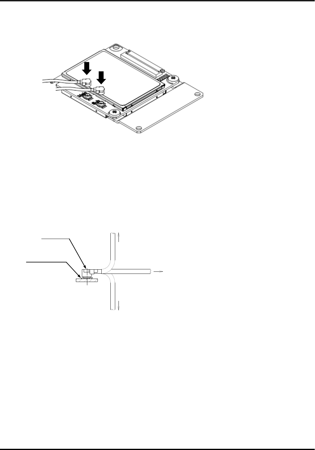
■Antenna connection
Please connect antennas as following figure.
・Do not pull the RF cable with too much force. It may cause damage to the RF connector
・Avoid an excessive twisting action upon connection or disconnection the connector as such an action can
cause damage to the connector.
・After connect fit, please do not add load more than that is shown in following figure to a cable.
●Permission load for the cable after the connector fit
1N or less(U.FL-LP(V)-040)
2N or less(U.FL-LP-040、U.FL-LP-066)
1N or less(U.FL-LP(V)-040)
2N or less(U.FL-LP-040、U.FL-LP-066)
3N or less(U.FL-LP(V)-040)
4N or less(U.FL-LP-040、U.FL-LP-066)
U.FL-R-SMT
U.FL-R-SMT-1
U.FL-LP
Harness type
Version 1.0
45
Operation mode
Communication mode
This device supports three communication modes. Only in roaming mode, this device supports the communication
method selection function.
●Supported communication mode
Communication mode
Description
Remarks
LTE mode (fixed)
Operated in LTE network only in Japan
Default
Roaming mode (fixed)
Operated out of Japan.
[Note1]
Auto selection mode
Select the communication mode (LTE or Roaming)
automatically
[Note1] Only in roaming mode, the communication method can be configuration by AT*KNWMODE.
Communication modes which can be selected are dual of WCDMA+GSM (default), WCDMA single and
GSM single.
・If flexible connector is used to connect to the external device, then only LTE mode can be available.
・Communication mode and method can be changed by AT command. And the configuration is stored in this
device.
・After the communication mode is changed by AT command, please reboot this device
・This device reports the UE Capability corresponding with the selected communication mode to the network.
●LTE mode
◆Supported communication method : LTE
◆Supported mobile phone career : only NTT DOCOMO
◆Roaming operation : None (Because LTE mode is used only in Japan)
●Roaming mode
◆Supported communication method : WCDMA, GSM
Configuration can be dual of WCDMA+GSM or WCDMA single or GSM single.
◆Supported mobile phone career : Mobile phone career out of Japan
Operation mode
Communication mode
Version 1.0
46
●Auto selection mode
(1)In this mode, this device selects the communication mode automatically.
(2)After this device selects the communication mode automatically, this device holds the communication mode
with the selected one, which is LTE mode or roaming mode.
(3)Actual working communication mode in auto selection mode can be confirmed by AT command.
(4)In this mode, this device selects the communication mode only at the time of start timing of this device. It
select the communication mode based on the condition of the radio environment (detected mobile phone
career).
●Condition to select the communication mode in auto selection mode
No.
Condition of radio environment
Selected mode
1
One or more Japanese mobile phone career is detected
LTE mode
2
Any mobile phone career is not detected
LTE mode
3
Only the mobile phone career out of Japan is detected
Roaming mode
●Precausion
Please note that the following description for the peculiar cases.
(1)In case that communication mode is roaming mode and communication method is dual of WCDMA+GSM or
WCDMA single, if Japanese mobile phone career is detected, this device will automatically reset with auto
selection mode.
(2)Because the accesses of this device is limited to only DOCOMO network in LTE mode operation, this device
never access to other mobile phone career in LTE communication method. If this device moves from inside
Japan to outside Japan in LTE mode operation, this device should be reset from the external device to keep
operation because this device does not have the function to detect the moving to outside Japan.
(3) If this device moves from outside Japan to inside Japan in roaming mode operation and GSM single method,
this device should be reset from the external device to keep operation because this device does not have the
function to detect the moving to inside Japan.

Version 1.0
47
Service function
Packet communication
The data communication speed this device supports is 112.5Mbps max for downlink and 37.5Mbps max for
uplink in LTE network, and 42.2Mbps max for downlink and 5.7Mbps max for uplink in W-CDMA network , and
237kbps for both downlink and uplink in GSM network.
【Summary of function】
・This device establishes PPP protocol for the external device with the trigger of originating or incoming
control by AT command. Then this device carries out the PDP/PDN link connection of radio segment
・This device configures the IP address of the external device using PPP. IPV4 and IPV6 are supported for IP
address.
・The interface which the external device can use in packet communication is UART and USB interface. Each
interface controls the packet communication independently. The multi PDP connection, that can do the
multiple communication in same time, is supported. Multi PDP connection is valid only in operation of LTE
communication mode.
・The USB interface provided to the external device is modem type (RAS method) and LAN type (NDIS
method).
・The incoming of packet communication incoming is supported only with modem type USB interface. It is not
supported with the LAN type USB interface.
■In case of the operation in LTE communication mode
・ At least one PDP type and APN must be configured. (The detail of PDP type and APN is described later.)
Please configure them by AT+CGDCONT.
・ The configuration of the peculiar function of LTE communication (packet communication and NDIS automatic
connection) is required.
Please configure it by AT*KALWAYSON.
■In case of the operation in roaming communication mode
・ The communication mode of this device must be configured.
Please configure it by AT*KNWMODE.
・ PDP type and APN must be configured before the packet communication.
Please configure it by AT+CGDCONT.
Service function
Packet communication
Version 1.0
48
■PDP type
This device supports two PDP type. They are PDP-Type=PPP and PDP-Type=IP.
In case of PDP-Type=IP, IPv4 and IPv6 can be configured as IP type.
Only IPv4 is supported as static IP address.
PDP-Type=PPP of LAN card type is not supported.
Please configure by AT+CGDCONT to suitable for the customer’s environment with considering above
condition.
●Supported IP address
PDP-Type
IPv4
IPv6
IPv4v6
Static
IPaddress
Dynamic
IPaddress
Static
IPaddress
Dynamic
IPaddress
Static
IPaddress
Dynamic
IPaddress
PPP(pseudo)
○
○
×
×
×
×
IP
○
○
×
○
×
×
○:Supported, ×:Not supported
■APN
In the packet communication, the LAN/ISP in the company to be accessed is appointed in the access point names
(APN) instead of phone number, and this device carries out dial-up connection using it. Please register the
Access Point Name (APN) for each connection point in this device prior to communication. And then, please
appoint the registration number (cid*) as the other party phone number to connect. For the connection to each
provider or LAN in the company, it is necessary to register the corresponding APN for each connection point.
The max number of APN can be configured in this device is twenty
Please configure the APN by AT+CGDCONT by terminal software.
At the factory shipment, APN is not configured.
The APN used in mock packet incoming is limited to the APN which corresponds to the CID configured by
AT*KALWAYSON
Version 1.0
49
SMS
This device supports the sending, receiving, storage and display of SMS (Short Message Service)
●Supported SMS service
Supported SMS service
Sending/Receiving
Remarks
General text SMS
Sending/Receiving
Supports linked SMS
Notification of SMS delivery
information
Receiving
-
Center push SMS
Receiving
-
●Supported SMS service for each communication mode
Supported SMS service
LTE mode
Roaming mode
Remarks
General text SMS
○
○
-
Notification of SMS delivery
information
○
○
-
Center push SMS
○
×
-
○:Supported, ×:Not supported
Area Mail
This device can receive earthquake early warning and tsunami warning delivered by the Japan Meteorological
Agency and disaster and evacuation information delivered by national and regional public institution.
■Supported Area Mail method
This device supports ETWS method. The ETWS method delivers the Area Mail to the external device faster by
using simple information notification.
Method
The process of the notification
ETWS
Notify the warning information by two steps. (two messages)
1. Notify only the simple information (warning for the earthquake and tsunami).
2. Notify the information about the warning by the Area Mail text.
■Supported Area Mail method for each communication mode
Method
LTE mode
Roaming mode
Remarks
ETWS
○
×
-
○:Supported, ×:Not supported
SMS
Area Mail

Version 1.0
50
Software update
Software update function is used to update its software via the LTE network to improve the functions of this device
after sale.
Because the communication between this device and the server in allocated in DOCOMO network to carry out
software update, this function is available only in DOCOMO network.
If other mobile phone career’s UIM card is used or this device is used outside of Japan, software update can not be
carried out.
■Software update method
This device supports the following two software update methods
(1) Software update from the network (PUSH type software update)
Software update is carried out by receiving the control SMS from server in DOCOMO network.
(2) Software update from the external device (PULL type software update)
Software update is carried out by receiving the AT command “AT*DSWU=0” from the external device.
RF part ON/ OFF function
This device has RF part ON/OFF function.
The status of RF part ON/OFF can be changed by AT+CFUN command.
Software update
RF part ON/OFF function

Version 1.0
51
AT command
AT command list
No.
Command
Function
1
ATA
Carry out manual operated incoming response of packet communication。
2
ATD
Carry out originating of packet communication。
3
ATE
Configure the echo existence or nonexistence for the sent command from the external device.
4
ATH
Disconnect the packet communication.
5
ATI
Display the product information about this device
6
ATO
Return to online data mode from online command mode
7
ATQ
Configure existence or nonexistence of result code sending after carrying out of the command
8
ATV
Configure the result code to numeric or English character
9
ATX
Configure the communication speed indication in the CONNECT indication at the time of packet connection
10
ATZ
Overwrite the configuration value of this device to the contents of the non-volatile memory
11
AT&C
Select the behavior of CD line to external device
12
AT&D
Select the behavior of this device by ER line in online data mode
13
AT&F
Initialize the configuration value of this device at the time of the factory shipment
14
AT&W
Store the configuration value of this device to non-volatile memory
15
AT&Z
Initialize the configuration value of this device and the contents of non-volatile memory to factory shipment
value
16
ATS0
Configure the number of times of RING until auto answer
17
ATS6
Configure the pose time until dialing
18
ATS7
Configure the wait time for the connection in packet communication after originating
19
ATS8
Configure the pose time (unit: sec) by comma dial.
20
ATS10
Configure the delay time for the automatic disconnection
21
ATS61
Display and reset the number of boot times by PWRKEY
22
ATS64
Display and reset the number of boot times by AT*DHWRST
23
ATS65
Display and reset the number of boot times by SYSRST button
24
AT¥S
Display the present configuration of this device
25
+++
Transfer from online data mode to online command mode
26
AT+GCAP
Display the supported range of AT command
27
AT+GMI
Display the manufacturer of this device
28
AT+GMM
Display the model (product name) of this device
29
AT+GMR
Display the version of this device
30
AT+IFC
Configure the flow control method between the external device and this device
31
AT+IPR
Configure the serial communication speed between the external device and this device
32
AT+CRON
Get the APN of previous incoming of packet communication
33
AT+PNRII
Display the restriction state of the network
34
AT*DANTE
Display the antenna level of this device.
35
AT*DHWRST
Carry out the hardware reset of this device
36
AT*DRPW
Display the indication of received radio wave power for this device
37
AT*DSWU
Carry out start and stop of the software update and confirm the state
38
AT+CCLK
Get the internal time information of this device
39
AT+CEER
Display the reason for previous disconnection of packet communication
40
AT+CGDCONT
Configure the access point name (APN) for packet communication
41
AT+CGMR
Display revision (IMEISV) of this device
42
AT+CGREG
Configure existence or nonexistence of display of +CGREG unsolicited result code in case of transferring to
in-service area from out-of-service area during packet communication
In addition, confirm the current state of in-service or out-of-service
43
AT+CGSN
Display the production number (IMEI) of this device
44
AT+CLCK
Enable or disable the PIN1 code and display the state of the PIN1 code
45
AT+CMEE
Configure the error report indication of this device
46
AT+CNUM
Display the phone number of the DOCOMO UIM card connected to this device
47
AT+CPAS
Inquire whether this device can send and receive the control signal.
48
AT+CPIN
Verify the PIN1 code and cancel the PIN1 code lock
49
AT+CPWD
Change PIN1 code
AT command
AT command list

Version 1.0
52
50
AT+CR
Configure existence or nonexistence of +CR (unsolicited result) display at the time of packet connection
51
AT+CRC
Configure existence or nonexistence of +CRING (unsolicited result) display at the time of packet incoming
52
AT+CREG
Configure existence or nonexistence of +CREG (unsolicited result) display when the state of circuit switching
area transfers from out-of-service area to in-service area
In addition, confirm the current state of in-service area or out-of-service area
53
AT+CSCS
Configure the character code used for output and input of SMS and Area Mail to/from the external device
54
AT+CMGD
Delete SMS
55
AT+CMGF
Configure the format of SMS and Area Mail
56
AT+CMGL
Display SMS and Area Mail of appointed state
57
AT+CMGR
Display SMS and Area Mail of appointed stored number
58
AT+CMGS
Send SMS
59
AT+CMGW
Store SMS in DOCOMO UIM card or this device
60
AT+CMSS
Send SMS stored in the memory
61
AT+CNMA
Notify the reception result to network at the time of receiving SMS
62
AT+CNMI
Configure the notification method at the time of receiving SMS and Area Mail
63
AT+CPMS
Configure the memory used for displaying, deleting and storing SMS and Area Mail
64
AT+CSCA
Configure SMS center number
65
AT+CSDH
Configure existence or nonexistence of indication of the detailed header information in the TEXT mode
66
AT+CSMP
Configure the parameter to send SMS in TEXT mode (AT+CMGF=1)
67
AT+CSMS
Configure the additional process of SMS message service
68
AT*DCHKLOC
Confirm radio wave environment at the time of the antenna setting
69
AT*DCHKANT
Display the condition whether communication is possible
70
AT*DPWROFF
Stop this device
71
AT*DTELNUM
Link the APN to the phone number and register them
72
AT*DCMGS
Send SMS directly
73
AT*DMEMFULL
Notify that SMS can not be received because of lack of stored area (memory full)
74
A/
Carry out again the previous carried out command
75
AT&P
Display the phone number stored in DOCOMO UIM card
76
AT!
Display the status of present this device
77
AT+CGACT
Carry out the connection and disconnection of NDIS.
Display the use condition for the CID configured by AT+CGDCONT
78
AT*KDEGSET
Configure the indication of the temperature in case that temperature becomes higher than the threshold.
79
AT*KDEG
Display the temperature of this device
80
AT+CFUN
Configure the ON/OFF of the RF part
81
AT+CEREG
Configure the indication of in-service or out-of-service for the LTE network
82
AT*KNWMODE
Configure the communication method
83
AT*KATMODE
Configure the operation mode of AT command
84
AT*KICCID
Display the identification number with 19 digits (ICCID) of UIM
85
AT*DLANTE
Display the LTE antenna level of this device.
86
AT*KINDSET
Configure the identification of SMS receiving, Area Mail receiving and arrival to the threshold temperature by
the signal line
87
AT*KMIMO
Configure the MIMO or not MIMO receiving
88
AT+COPS
Configure the PLMN (MCC + MNC) in roaming mode operation
89
AT*KCMGR
Display the linked SMS
90
AT*KCMGD
Delete the linked SMS
91
AT*KCNMI
Configure the indication method at the time of linked SMS receiving
92
AT*KNDIS
Configure the parameter of manual NDIS connection
93
AT*KALWAYSON
Configure the parameter of Always-ON connection
FCC Regulatory notices
Modification statement
“Hitachi Kokusai Electric Inc.” has not approved any changes or modifications to this device by the user. Any
changes or modifications could void the user’s authority to operate the equipment.
Interference statement
This device complies with Part 15 of the FCC Rules. Operation is subject to the following two conditions: (1)
this device may not cause interference, and (2) this device must accept any interference, including interference
that may cause undesired operation of the device.
Wireless notice
This equipment complies with FCC radiation exposure limits set forth for an uncontrolled environment. The
antenna should be installed and operated with minimum distance of 20 cm between the radiator and your body.
Antenna gain must be as below:
Frequency band Maximum antenna gain
GSM 850/FDD V 3.42 dBi
PCS 1900 2.01 dBi
This transmitter must not be co-located or operating in conjunction with any other antenna or transmitter.
FCC Class B digital device notice
This equipment has been tested and found to comply with the limits for a Class B digital device, pursuant to
part 15 of the FCC Rules. These limits are designed to provide reasonable protection against harmful
interference in a residential installation. This equipment generates uses and can radiate radio frequency energy
and, if not installed and used in accordance with the instructions, may cause harmful interference to radio
communications. However, there is no guarantee that interference will not occur in a particular installation. If
this equipment does cause harmful interference to radio or television reception, which can be determined by
turning the equipment off and on, the user is encouraged to try to correct the interference by one or more of the
following measures:
- Reorient or relocate the receiving antenna.
- Increase the separation between the equipment and receiver.
- Connect the equipment into an outlet on a circuit different from that to which the receiver is connected.
- Consult the dealer or an experienced radio/TV technician for help.
Labelling Requirements for the Host device
The host device shall be properly labelled to identify the modules within the host device. The certification label
of the module shall be clearly visible at all times when installed in the host device, otherwise the host device
must be labelled to display the FCC ID of the module, preceded by the words "Contains transmitter module", or
the word "Contains", or similar wording expressing the same meaning, as follows:
Contains FCC ID: TTIUM04KO
53

1999/5/EC Directive regulatory notices
This device has been evaluated against the essential requirements of the 1999/5/EC Directive.
Bulgarian
С настоящето ““Hitachi Kokusai Electric Inc.” декларира, че ““UM04-KO”отговаря на съществените изисквания и
другите приложими изисквания на Директива 1999/5/ЕС.
Croatian
Ovime “Hitachi Kokusai Electric Inc.”, izjavljuje da je ovaj “UM04-KO” je u skladu s osnovnim zahtjevima i drugim
relevantnim odredbama Direktive 1999/5/EC.
Czech
““Hitachi Kokusai Electric Inc.” tímto prohlašuje, že tento ““UM04-KO”je ve shodě se základními požadavky a dalšími
příslušnými ustanoveními směrnice 1999/5/ES.
Danish
Undertegnede ““Hitachi Kokusai Electric Inc.” erklærer herved, at følgende udstyr ““UM04-KO”overholder de
væsentlige krav og øvrige relevante krav i direktiv 1999/5/EF.
Dutch
Hierbij verklaart ““Hitachi Kokusai Electric Inc.” dat het toestel ““UM04-KO”in overeenstemming is met de essentiële
eisen en de andere relevante bepalingen van richtlijn 1999/5/EG.
English
Hereby, ““Hitachi Kokusai Electric Inc.”, declares that this ““UM04-KO”is in compliance with the essential requirements
and other relevant provisions of Directive 1999/5/EC.
Estonian
Käesolevaga kinnitab ““Hitachi Kokusai Electric Inc.” seadme ““UM04-KO”vastavust direktiivi 1999/5/EÜ põhinõuetele
ja nimetatud direktiivist tulenevatele teistele asjakohastele sätetele.
German
Hiermit erklärt ““Hitachi Kokusai Electric Inc.”, dass sich das Gerät ““UM04-KO”in Übereinstimmung mit den
grundlegenden Anforderungen und den übrigen einschlägigen Bestimmungen der Richtlinie 1999/5/EG befindet.
Greek
ΜΕ ΤΗΝ ΠΑΡΟΥΣΑ ““Hitachi Kokusai Electric Inc.” ΔΗΛΩΝΕΙ ΟΤΙ ““UM04-KO”ΣΥΜΜΟΡΦΩΝΕΤΑΙ ΠΡΟΣ ΤΙΣ
ΟΥΣΙΩΔΕΙΣ ΑΠΑΙΤΗΣΕΙΣ ΚΑΙ ΤΙΣ ΛΟΙΠΕΣ ΣΧΕΤΙΚΕΣ ΔΙΑΤΑΞΕΙΣ ΤΗΣ ΟΔΗΓΙΑΣ 1999/5/ΕΚ.
Hungarian
Alulírott, ““Hitachi Kokusai Electric Inc.” nyilatkozom, hogy a ““UM04-KO”megfelel a vonatkozó alapvetõ
követelményeknek és az 1999/5/EC irányelv egyéb elõírásainak.
Finnish
““Hitachi Kokusai Electric Inc.” vakuuttaa täten että ““UM04-KO”tyyppinen laite on direktiivin 1999/5/EY oleellisten
vaatimusten ja sitä koskevien direktiivin muiden ehtojen mukainen.
French
Par la présente ““Hitachi Kokusai Electric Inc.” déclare que l'appareil ““UM04-KO”est conforme aux exigences
essentielles et aux autres dispositions pertinentes de la directive 1999/5/CE.
Icelandic
Hér með lýsir ““Hitachi Kokusai Electric Inc.” yfir því að ““UM04-KO”er í samræmi við grunnkröfur og aðrar kröfur,
sem gerðar eru í tilskipun 1999/5/EC
Italian
Con la presente ““Hitachi Kokusai Electric Inc.” dichiara che questo ““UM04-KO”è conforme ai requisiti essenziali ed
alle altre disposizioni pertinenti stabilite dalla direttiva 1999/5/CE.
Latvian
Ar šo ““Hitachi Kokusai Electric Inc.” deklarē, ka ““UM04-KO”atbilst Direktīvas 1999/5/EK būtiskajām prasībām un
citiem ar to saistītajiem noteikumiem.
Lithuanian
Šiuo ““Hitachi Kokusai Electric Inc.” deklaruoja, kad šis ““UM04-KO”atitinka esminius reikalavimus ir kitas 1999/5/EB
Direktyvos nuostatas.
Maltese
Hawnhekk, ““Hitachi Kokusai Electric Inc.”, jiddikjara li dan ““UM04-KO”jikkonforma mal-ħtiġijiet essenzjali u ma
provvedimenti oħrajn relevanti li hemm fid-Dirrettiva 1999/5/EC.
Norwegian
““Hitachi Kokusai Electric Inc.” erklærer herved at utstyret ““UM04-KO”er i samsvar med de grunnleggende krav og
øvrige relevante krav i direktiv 1999/5/EF.
Polish
Niniejszym ““Hitachi Kokusai Electric Inc.” oświadcza, że ““UM04-KO”jest zgodny z zasadniczymi wymogami oraz
pozostałymi stosownymi postanowieniami Dyrektywy 1999/5/EC
Portuguese
““Hitachi Kokusai Electric Inc.” declara que este ““UM04-KO”está conforme com os requisitos essenciais e outras
disposições da Directiva 1999/5/CE.
Slovak
““Hitachi Kokusai Electric Inc.” týmto vyhlasuje, že ““UM04-KO”spĺňa základné požiadavky a všetky príslušné
ustanovenia Smernice 1999/5/ES.
Slovenian
““Hitachi Kokusai Electric Inc.” izjavlja, da je ta ““UM04-KO”v skladu z bistvenimi zahtevami in ostalimi relevantnimi
določili direktive 1999/5/ES.
Spanish Por medio de la presente ““Hitachi Kokusai Electric Inc.” declara que ““UM04-KO”cumple con los requisitos esenciales
y cualesquiera otras disposiciones aplicables o exigibles de la Directiva 1999/5/CE.
Swedish Härmed intygar ““Hitachi Kokusai Electric Inc.” att denna ““UM04-KO”står I överensstämmelse med de väsentliga
egenskapskrav och övriga relevanta bestämmelser som framgår av direktiv 1999/5/EG.
54
In order to satisfy the essential requirements of 1999/5/EC Directive, the product is compliant with the following standards:
RF spectrum use (R&TTE art. 3.2)
EN 301 511 V9.0.2
EN 301 908-1 V6.2.1
EN 301 908-2 V6.2.1
EN 301 908-13 V6.2.1
EMC (R&TTE art. 3.1b)
EN 301 489-1 V1.9.2
EN 301 489-7 V1.3.1
EN 301 489-24 V1.5.1
Health & Safety (R&TTE art. 3.1a)
EN 60950-1:2006 + A11:2009 + A1:2010 + A12:2011 + AC:2011
+ A2: 2013
The conformity assessment procedure referred to in Article 10 and detailed in Annex IV of Directive 1999/5/EC has been followed
with the involvement of the following Notified Body:
AT4 wireless, S.A.
Parque Tecnologico de Andalucía
C/ Severo Ochoa 2
29590 Campanillas – Málaga
SPAIN
Notified Body No: 1909
Thus, the following marking is included in the product:
There is no restriction for the commercialization of this device in all the countries of the European Union.
Final product integrating this module must be assessed against essential requirements of the 1999/5/EC (R&TTE) Directive. It should
be noted that assessment does not necessarily lead to testing. Hitachi Kokusai Electric Inc. recommends carrying out the following
assessments:
RF spectrum use (R&TTE art. 3.2)
It will depend on the antenna used on the final product.
EMC (R&TTE art. 3.1b)
Testing
Health & Safety (R&TTE art. 3.1a)
Testing
55