Honeycomb Technologies HRF24A13AN RF 2.4G module User Manual manual
Shenzhen Honeycomb Technologies Company Limited RF 2.4G module manual
UserManual.wiki
>
Honeycomb Technologies
>
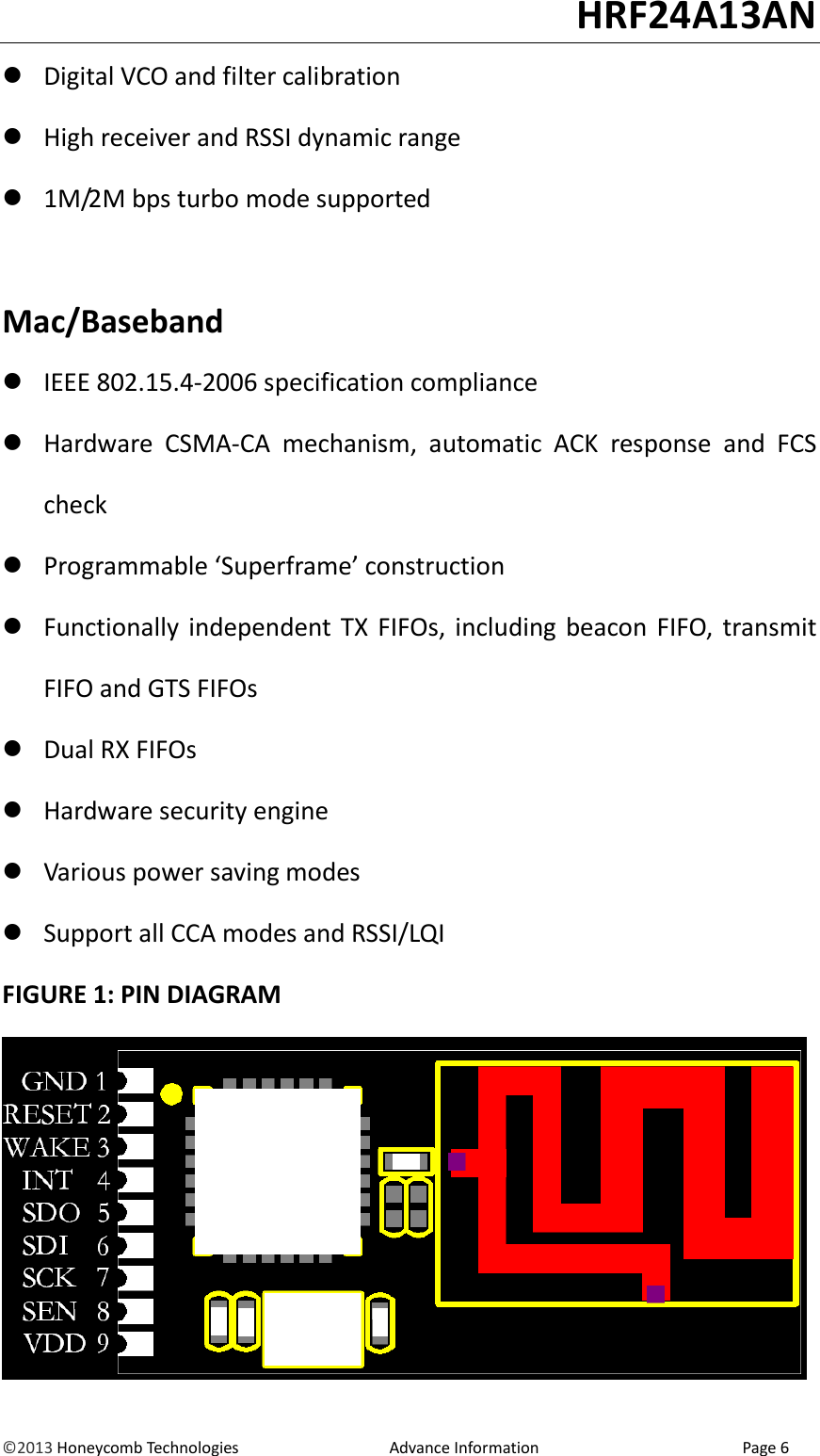
HRF24A13AN User Manual
User Manual
Navigation menu
Upload a User Manual
Namespaces
Wiki Guide
HTML
PDF
Info
Views
User Manual
Discussion / Help
Navigation