Honeycomb Technologies HRF24A13AN RF 2.4G module User Manual manual
Shenzhen Honeycomb Technologies Company Limited RF 2.4G module manual
User Manual

HRF24A13AN
©2013 Honeycomb Technologies Advance Information Page 1
HRF24A13AN
Data Sheet
2.4 GHz IEEE Std. 802.15.4™
RF Transceiver Module
HRF24A13AN
©2013 Honeycomb Technologies Advance Information Page 2
Note the label artwork for Products
Warning: Changes or modifications to this unit not expressly approved by the party
responsible for compliance could void the user’s authority to operate the equipment.
NOTE: This equipment has been tested and found to comply with the limits for a Class B
digital device, pursuant to Part 15 of the FCC Rules. These limits are designed to provide
reasonable protection against harmful interference in a residential installation. This
equipment generates, uses and can radiate radio frequency energy and, if not installed and
used in accordance with the instructions, may cause harmful interference to radio
communications.
However, there is no guarantee that interference will not occur in a particular installation. If
this equipment does cause harmful interference to radio or television reception, which can be
determined by turning the equipment off and on, the user is encouraged to try to correct the
interference by one or more of the following measures:
Reorient or relocate the receiving antenna.
Increase the separation between the equipment and receiver.
Connect the equipment into an outlet on a circuit different from that to which the
receiver is connected.
Consult the dealer or an experienced radio/TV technician for help.

HRF24A13AN
©2013 Honeycomb Technologies Advance Information Page 3
Note: This 2.4G RF Module is designed to be used internally only in Controls
products which with RF shielding. It is not intended to be sold as an end item by
itself to external customers.
FCC Caution: Any changes or modifications not expressly approved by the party
responsible for compliance could void the user’s authority to operate this
equipment.
This module and its antenna(s) must not be co-located with any other transmitters
except in accordance with FCC multi-transmitter product procedures.
The module is intended only for OEM integrator. And it should not be marketed
and sold in a way that has to be end-user accessible / replaceable. The host
product is required to comply with all applicable FCC equipment authorizations
regulations, requirements and equipment functions not associated with the
transmitter module portion. The host manufacturer is responsible for ensuring
compliance with the module(s) installed and fully operational.
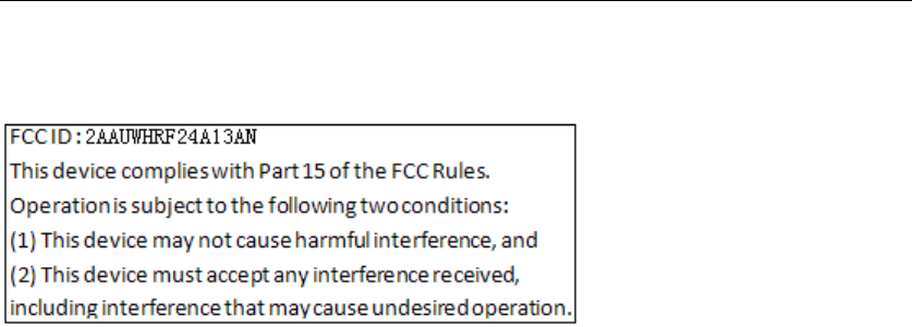
Label of the end product:
The final end product must be labeled in a visible area with the following “Contains
Transmitter Module FCC ID: 2AAUWHRF24A13AN” or “Contains FCC ID:
2AAUWHRF24A13AN”. If the size of the end product is larger than 8*10cm, then
the following FCC Part 15.19 statement has to also be available on the label: This
device complies with Part 15 of the FCC Rules. Operation is subject to the following
two conditions: (1) this device may not cause harmful interference, and (2) this
device must accept any interference received, including interference that may
cause undesired operation.
User manual of the end product:
In the user manual of the end product, the end user has to be informed that:
Warning: Changes or modifications to this unit not expressly approved by the party
responsible for compliance could void the user’s authority to operate the equipment.
NOTE: This equipment has been tested and found to comply with the limits for a Class B
digital device, pursuant to Part 15 of the FCC Rules. These limits are designed to provide
reasonable protection against harmful interference in a residential installation. This
equipment generates, uses and can radiate radio frequency energy and, if not installed and
used in accordance with the instructions, may cause harmful interference to radio
communications.
However, there is no guarantee that interference will not occur in a particular installation. If
this equipment does cause harmful interference to radio or television reception, which can be
determined by turning the equipment off and on, the user is encouraged to try to correct the
interference by one or more of the following measures:

HRF24A13AN
©2013 Honeycomb Technologies Advance Information Page 4
Reorient or relocate the receiving antenna.
Increase the separation between the equipment and receiver.
Connect the equipment into an outlet on a circuit different from that to which the
receiver is connected.
Consult the dealer or an experienced radio/TV technician for help.
If the size of the end product is smaller than 8*10cm, then additional FCC Part
15.19 statement is required to be available in the user manual: This device
complies with Part 15 of the FCC Rules. Operation is subject to the following two
conditions: (1) this device may not cause harmful interference, and (2) this device
must accept any interference received, including interference that may cause
undesired operation.

HRF24A13AN
©2013 Honeycomb Technologies Advance Information Page 5
2.4 GHz IEEE Std. 802.15.4™ RF Transceiver Module
Features:
IEEE 802.15.4-2006 Compliant RF Transceiver
Small Size: 25mm*11.8mm Surface Mountable
Integrated Crystal, Internal Voltage Regulator, Matching Circuitry and
PCB Antenna.
Radio Regulation Certification for United States (FCC ID)
Up to 300m Range (outdoor, line-of-sight)
Operational:
Operating Voltage: 2.4V-3.6V(3.3V typical)
Temperature Range: -20°C to +70°C
Simple, Four-Wire SPI Interface
RF/Analog
ISM band 2.405~2.475 GHz operation
Integrated low phase noise VCO, frequency synthesizer and PLL loop
filter
Integrated 32 MHz oscillator drive
Integrated internal oscillator circuit
Single End RF input/output
32 MHz reference clock output
HRF24A13AN
©2013 Honeycomb Technologies Advance Information Page 6
Digital VCO and filter calibration
High receiver and RSSI dynamic range
1M/2M bps turbo mode supported
Mac/Baseband
IEEE 802.15.4-2006 specification compliance
Hardware CSMA-CA mechanism, automatic ACK response and FCS
check
Programmable ‘Superframe’ construction
Functionally independent TX FIFOs, including beacon FIFO, transmit
FIFO and GTS FIFOs
Dual RX FIFOs
Hardware security engine
Various power saving modes
Support all CCA modes and RSSI/LQI
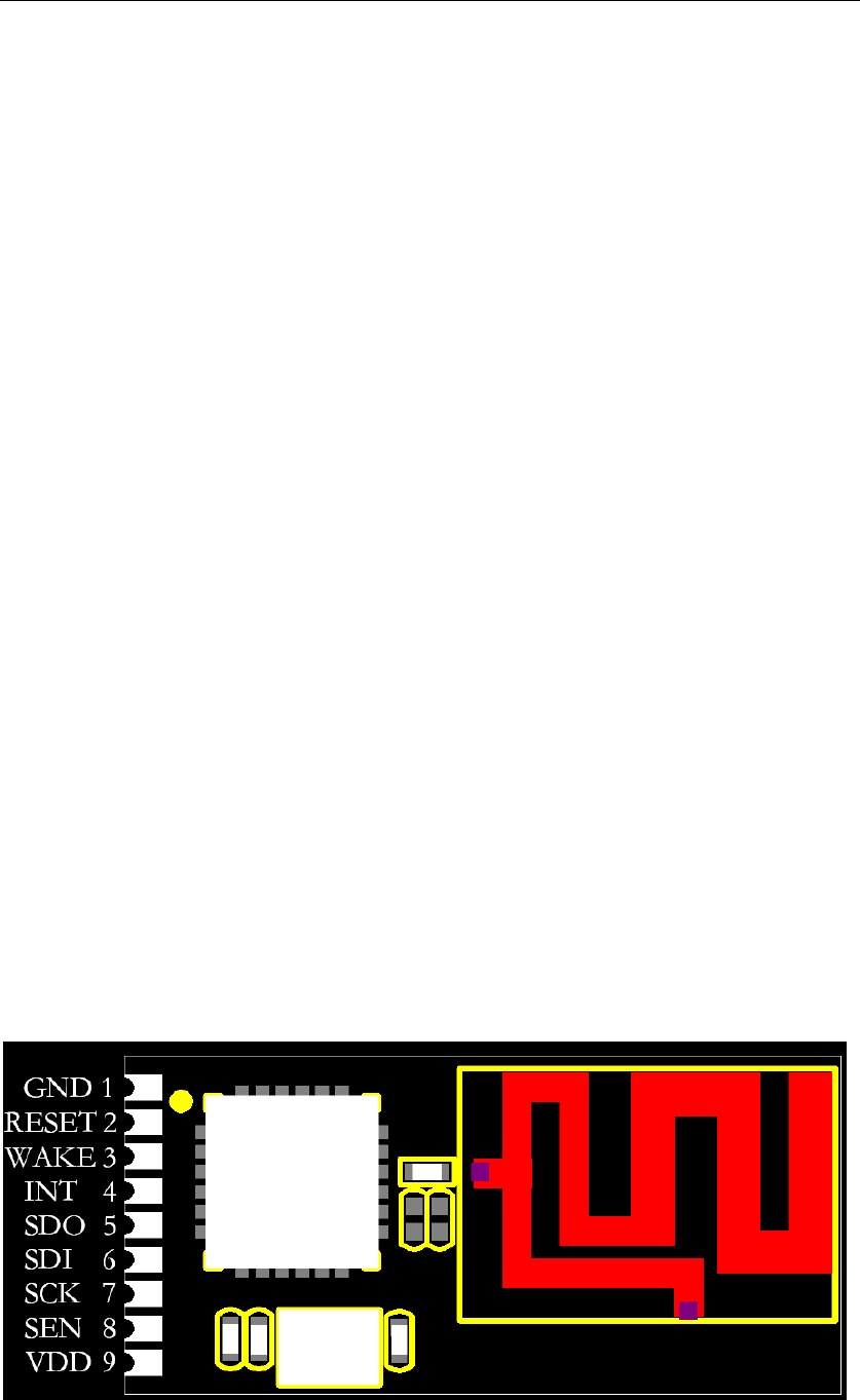
FIGURE 1: PIN DIAGRAM
HRF24A13AN
©2013 Honeycomb Technologies Advance Information Page 7
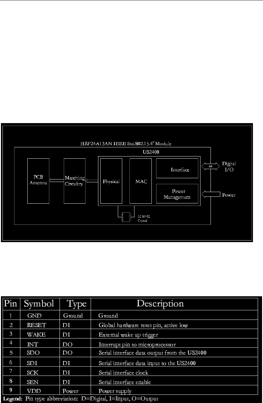
Device Overview
HRF24A13AN is a solution that complies with IEEE 802.15.4-2006 specifications. It
integrates a 2.4 GHz RF transceiver with an IEEE802.15.4 compliant Baseband/MAC
block within a single chip. The HRF24A13AN can be controlled by a microprocessor
(e.g. 8051) for low-data-rate applications such as home automation, industrial
automation, consumer electronics, PC peripheral …etc. For medium-data-rate
applications like wireless voice and image transmission, the HRF24A13AN provides
1M/2M bps turbo mode.
FIGURE 2: BLOCK DIAGRAM
TABLE 1-1: PIN DESCRIPTION
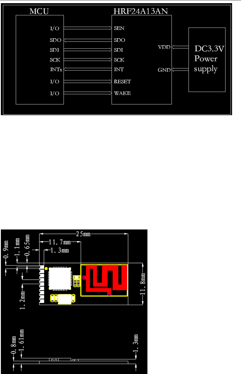
FIGURE 3: MICROCONTROLLER TO HRF24A13AN INTERFACE
HRF24A13AN
©2013 Honeycomb Technologies Advance Information Page 8
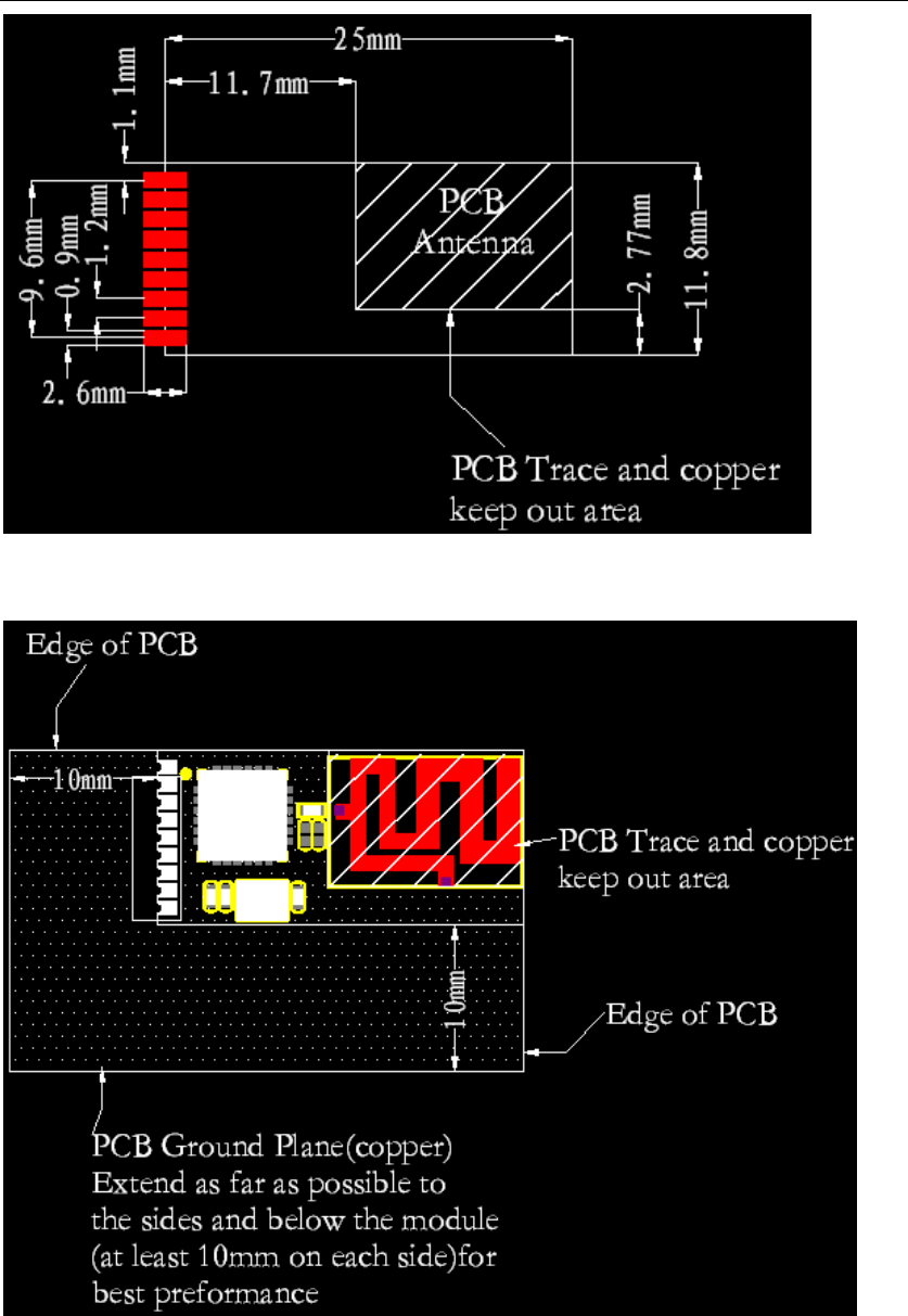
Mounting Details
The HRF24A13AN is a surface mountable module. Module dimensions are shown in
Figure 4. The module Printed Circuit Board (PCB) is 0.032" thick with castellated
mounting holes on the edge. Figure 5 is a recommended host PCB footprint for the
HRF24A13AN. The HRF24A13AN has an integrated PCB antenna. For the best
performance, follow the mounting details shown in Figure 6. It is recommended that
the module be mounted on the edge of the host PCB and an area around the
antenna, approximately 1.2", be kept clear of metal objects. A host PCB ground plane
around the HRF24A13AN acts as a counterpoise to the PCB antenna. It is
recommended to extend the ground plane at least 0.4" around the module.
FIGURE 4: MODULE DETAILS
FIGURE 5 RECOMMENDED PCB FOOTPRINT
HRF24A13AN
©2013 Honeycomb Technologies Advance Information Page 9
FIGURE 6 MOUNTING DETAILS
CIRCUIT DESCRIPTION
HRF24A13AN
©2013 Honeycomb Technologies Advance Information Page 10
The HRF24A13AN is a complete 2.4 GHz IEEE 802.15.4-2006 compliant surface mount
module with integrated crystal, internal voltage regulator, matching circuitry and PCB
antenna. The HRF24A13AN module interfaces to many popular micro-controllers via
a 4-wire serial SPI interface, interrupt, wake, Reset, power and ground.
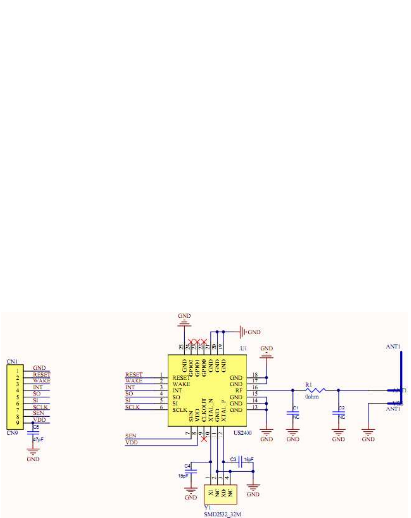
SCHEMATIC
A schematic diagram of the module is shown in Figure 7 and the Bill of Materials
(BOM) is shown in Table 2. The HRF24A13AN module is based on the Ubec
Technology US2400 IEEE 802.15.4-2006 GHz RF Transceiver IC. The serial I/O (SCK,
SDI, SDO and CS), RESET, WAKE, INT and CLKOUT pins are brought out to the module
pins. The SDO signal is tri-state buffered by IC2 to solve a silicon errata where the
SDO signal does not release to a high-impedance state after the CS pin returns to its
inactive state. Crystal Y1 is a 32 MHz crystal with a frequency tolerance of ±20 ppm
@ 25°C to meet the IEEE 802.15.4-2006 symbol rate tolerance of ±40 ppm. A balun is
formed by components: C21,C2 and R1. C5 is a DC block capacitor.
FIGURE 7 HRF24A13AN SCHEMATIC
TABLE 2
HRF24A13AN BILL OF MATERIALS
HRF24A13AN
©2013 Honeycomb Technologies Advance Information Page 11
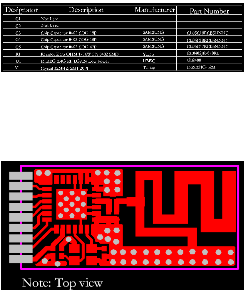
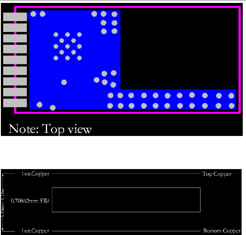
Printed Circuit Board
The HRF24A13AN module printed circuit board is con-structed with FR4 material,
two layers and 0.8mm thick. The layers are shown in Figure 8 through Figure 9. The
stack up of the PCB is shown in Figure10
FIGURE 8 TOP COPPER
FIGURE 9 BOTTOM COPPER
HRF24A13AN
©2013 Honeycomb Technologies Advance Information Page 12
FIGURE 10 PCB LAYER STACK UP
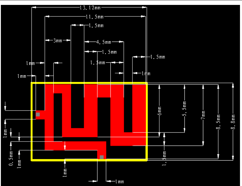
PCB Antenna
The PCB antenna is fabricated on the top copper trace. Figure 11 shows the trace
dimensions. The layers below the antenna have no copper traces. The ground and
power planes under the components serve as a counterpoise to the PCB antenna.
Additional ground plane on the host PCB will substantially enhance the performance
of the module.
FIGURE 11 PCB LAYER STACK UP
HRF24A13AN
©2013 Honeycomb Technologies Advance Information Page 13