Honeywell ALA-52B2 Radio Altimeter User Manual CMM ALA 52B Radio Altimeter 012 0823 001
Honeywell International Inc. Radio Altimeter CMM ALA 52B Radio Altimeter 012 0823 001
UserManual.wiki
>
Honeywell
>
ALA 52B2 User Manual
Users Manual
Navigation menu
Upload a User Manual
Namespaces
Wiki Guide
HTML
PDF
Info
Views
User Manual
Discussion / Help
Navigation

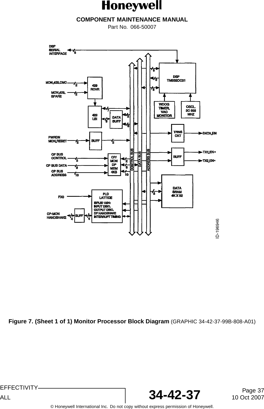
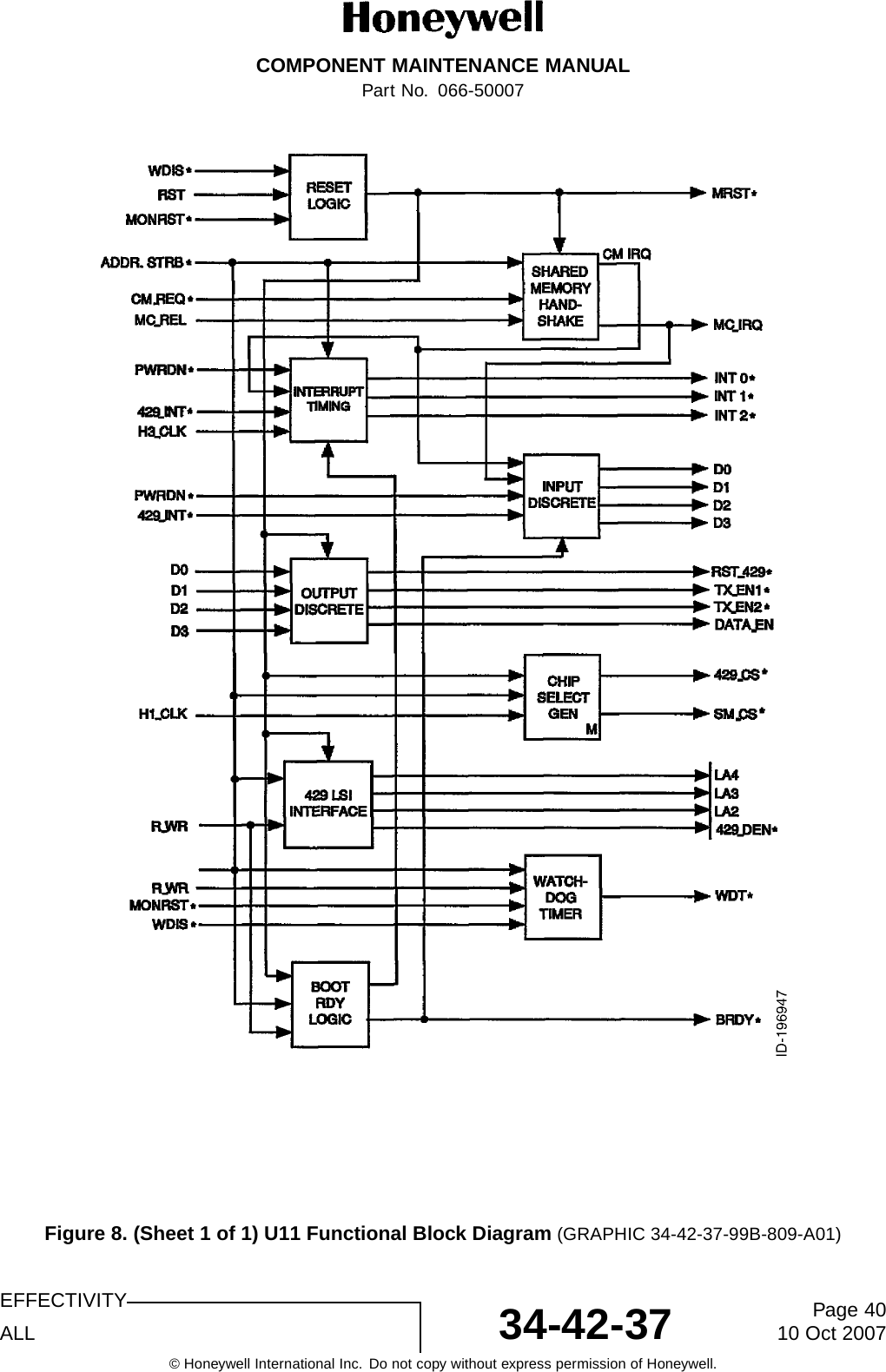
![COMPONENT MAINTENANCE MANUALPart No. 066-50007to the DSP_DATA [31:0] bus where the microprocessor has access tothe contents of the FIFO.2Another mode of operation is byte sampling. The microprocessor determinesthat it wants to look at either the RX_MUX on J10/J2-20 from the RF controlmodule or the bit MUX U43. This allows the microprocessor to monitordifferent voltages. The BIT output has a MUX on the RF control module,which allows the microprocessor to monitor RF test points.3The BIT MUX U43 enables a monitor of the power supply voltages +24,+12, and -12 and also a loop back DAC output (DAC8_0). Inputs DSPBD0,1 and 2 are used to determine which one of the inputs is monitored. TheDSP U15 writes to a latch inside the MUX U43 to select which of the 8inputs it is going to look at.(d) DSP Memory Circuits1The output of the FIFOs U18 and U29 is accessed by U15, which is the DSP.The DSP processes the difference frequency and calibration frequency intoaltitude information2Memory devices U6, U7, U12, and U23 are 32 k X 8 SRAMs, which make upthe program/data memory. These are zero wait state memories that use 15nanosecond RAMs that are 32 k deep. This makes a 32 k by 32-bit RAMarray where the program is stored after boot up.3Dual ported RAM U33 is a where the communications between the DSP andthe main processor takes place. It is 4 k deep by 8-bit wide where by themain processor and DSP can access any location. It is partitioned so theDSP does not access the main processor portion of the RAM. This is whereall the commands from the main processor go to the DSP, and the altitudespectrum data from the DSP goes to the main processor.(e) Data Buffers and Latches1Device U44 is a 16-bit data bus buffer. This is divided into two 8-bitfunctions. The U44 (1A) and U44 (1B) function buffers the lower 8-bits ofthe data bus. On U44 (1B) there is a DSPD0 signal, which is not buffered,that passes through U44 and comes out as DSPBD0, which is buffered.The other function U44 (2A) and U44 (2B) reads the discrete inputs fromthe RF control module. RF1_FIN0 and RF2_FIN0 are functions, which aredefined, on the RF control module.2Latch U35 is a 16-bit latch, which supplies latched outputs to the RF controlmodule. Data outputs DSPBD0 thru DSPBD7 is the buffered data bus andDSPD8 thru DSPD15 is unbuffered data. Outputs DSPL0 thru DSPL15 gothrough 5 megahertz low pass filters U14 and U58. They are then routed tothe two connectors going to the RF control module.(f) Digital to Analog Circuits1DAC U41 is a quad 8-bit device. Output 0 of U41 goes through another filterU30 and is routed to the RF control module on connector J10-28, as IF AGCvoltage. This voltage allows the DSP to control the gain of the receiver IF.EFFECTIVITYALL 34-42-37 Page 3110 Oct 2007© Honeywell International Inc. Do not copy without express permission of Honeywell.](https://usermanual.wiki/Honeywell/ALA-52B2/User-Guide-901606-Page-29.png)