Honeywell ALA-52B2 Radio Altimeter User Manual CMM ALA 52B Radio Altimeter 012 0823 001
Honeywell International Inc. Radio Altimeter CMM ALA 52B Radio Altimeter 012 0823 001
Users Manual
COMPONENT MAINTENANCE MANUAL
Part No. 066-50007
DESCRIPTION AND OPERATION
1. Description (TASK 34-42-37-870-801-A01)
A. General (Subtask 34-42-37-870-001-A01)
(1) This section contains descriptive information covering the ALA-52B Radio Altimeter
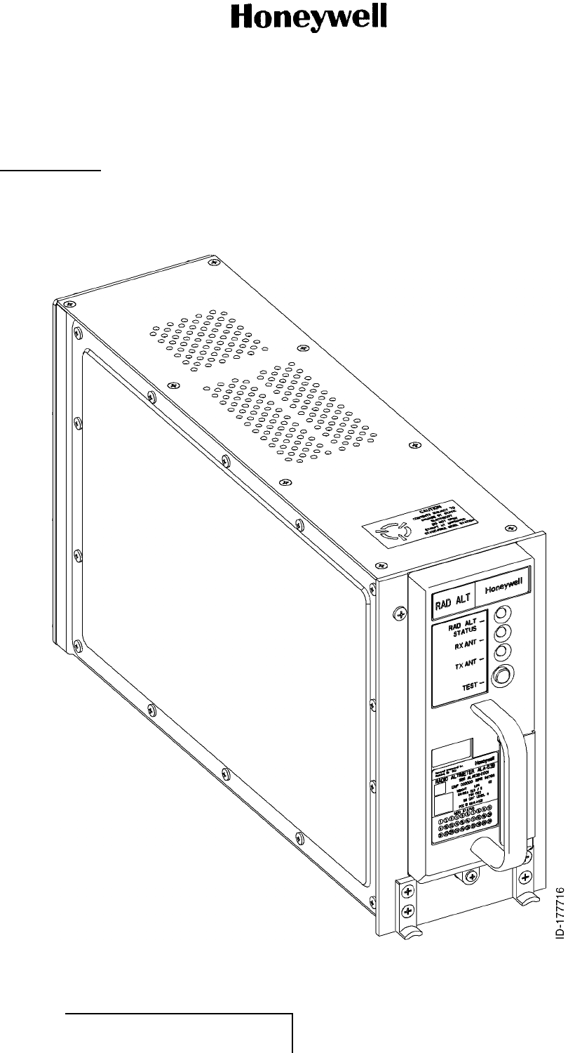
(ALA-52B). The ALA-52B is shown in Figure 1 (GRAPHIC 34-42-37-99B-802-A01).
Figure 1. (Sheet 1 of 1) ALA-52B Radio Altimeter (GRAPHIC 34-42-37-99B-802-A01)
EFFECTIVITY
ALL 34-42-37 Page 1
10 Oct 2007
© Honeywell International Inc. Do not copy without express permission of Honeywell.

COMPONENT MAINTENANCE MANUAL
Part No. 066-50007
(2) The ALA-52B is part of the Honeywell ALA-52B Radio Altimeter System. The
ALA-52B is a lightweight, solid-state, digital airborne altimeter designed to provide
accurate, digital height measurements above terrain during aircraft approach, landing,
and climb-out phases. It is a low-range altimeter that incorporates two different and
independent microprocessors, one of which performs the primary altitude computation
while the second independently verifies the computation by comparison.
2. Configuration (TASK 34-42-37-870-802-A01)
A. Overview (Subtask 34-42-37-870-002-A01)
(1) Table 1 lists the features contained in the ALA-52B. Table 2 contains a brief description
of each feature.
Table 1. ALA-52B Configurations
Features
Honeywell
Part Number
066-50007 Basic Unit Fault Memory CMC
Compatible Maximum
Weight (Lbs/Kg)
-1111 XXX8.6/3,9
Table 2. ALA-52B Features
Feature Description
Basic Unit Airborne solid-state radio altimeter that incorporates
two different and independent microprocessors, one
of which performs the primary altitude computation
while the second independently verifies the
computation by comparison. The altitude information
is supplied to the AFCS and height displays on the
instrument panel. The front panel contains LEDs
that indicate the operating status of the unit. The
front panel also provides a user interface for test
and troubleshooting, including a test button and an
RS-232C 25-pin “D” connector. The RS-232 front
panel connector is used for testing the ALA-52B
through a front panel adapter.
Fault Memory A nonvolatile, single-chip fault memory that allows
the recording of faults associated with a particular
flightleg. Sixty-four flight legs are available with each
flight leg made up of a flightleg information header
containing a fault record section for recording ten
airborne faults and three ground faults. When all
flight legs are used, the oldest flight leg is reused.
CMC Interface The ALA-52B interfaces fault memory and BITE
data between radio altimeter and line maintenance
CMC for the purpose of extracting maintenance
information and initiating tests. Designed to conform
with ARINC 429 interfaces, and ARINC 604.
EFFECTIVITY
ALL 34-42-37 Page 2
10 Oct 2007
© Honeywell International Inc. Do not copy without express permission of Honeywell.

COMPONENT MAINTENANCE MANUAL
Part No. 066-50007
3. Leading Particulars (TASK 34-42-37-870-803-A01)
A. Unit Specifications (Subtask 34-42-37-870-003-A01)
(1) Table 3 lists the leading particulars for the ALA-52B.
Table 3. ALA-52B Leading Particulars
Characteristics Description
Form Factor ARINC6003MCU
Dimensions 14.04 in. (35,66 cm) long by 3.56 in. (9,04 cm) wide by 7.64 in.
(19,41 cm) high
Weight 8.6lb(3,9Kg)maximum
Power Requirements 30W, +28 V dc
Temperature:
• Operating 5to+158 F(-15to+70 C)
•Storage -67to+185 F(-55to+85 C)
Cooling ARINC 600 forced air
Humidity Zero to 95% relative humidity at 122 F(50 ºC)
Altitude 50,000 ft (15,240 m) above mean sea level
Warm-up period Stable operation within 6 seconds
Frequency Range 4.235 to 4.365 GHz
Transmit Power +26 dBm (nominal at antenna port)
Operating Range of Altitudes -20 to 5000 ft (-6,1 to 1524 m)
Accuracy ±1.5 ft (0,46 m) or 2%, whichever is greater
Data Outputs ARINC 429 range and CMC interface
Aircraft Installation Delays 40, 57, 80 ft
Pitch Limits ±20º
Roll Limits ±40º
Doppler Error Compensated using dual slope FM ramp
Self-Test Automatic in-flight, manual from discrete, ARINC 429, or front panel
Integrity Monitoring Continuous self-monitoring establishes operational status at all
altitudes
Fault Reporting Conforms to Boeing 777 formats
B. Environmental Certification (Subtask 34-42-37-870-004-A01)
(1) The ALA-52B meets the environmental conditions of the RTCA document
number DO-160E, Environmental Conditions and Test Procedures for Airline
Electronic/Electrical Equipment and Instruments. Refer to Table 4.
EFFECTIVITY
ALL 34-42-37 Page 3
10 Oct 2007
© Honeywell International Inc. Do not copy without express permission of Honeywell.

COMPONENT MAINTENANCE MANUAL
Part No. 066-50007
Table 4. Environmental Certification Categories of ALA-52B
Test Category
Temperature and Altitude A2/B2
In-Flight Loss of Cooling Z
Temperature Variation B
Humidity A
Operational Shocks and Crash Safety B
Vibration S
Vibration Curves B
Explosion Atmosphere X
Waterproofness X
Fluids Susceptibility X
Sand and Dust X
Fungus Resistance X
Salt Spray X
Magnetic Effect A
Power Input A
Voltage Spike A
Audio Frequency Conducted Susceptibility - Power
Inputs R
Induced Signal Susceptibility ZC
Radio Frequency Susceptibility (Radiated and
Conducted) WE
Emission of Radio Frequency Energy M
Lightning Induced Transient Susceptibility ZZZZZ
Lightning Direct Effects X
Icing X
Electrostatic Discharge A
Fire, Flammability C
NOTE: Category X = Test not applicable.
EFFECTIVITY
ALL 34-42-37 Page 4
10 Oct 2007
© Honeywell International Inc. Do not copy without express permission of Honeywell.

COMPONENT MAINTENANCE MANUAL
Part No. 066-50007
4. Brief Description of Equipment (TASK 34-42-37-870-804-A01)
A. Mechanical Description (Subtask 34-42-37-870-005-A01)
(1) The ALA-52B is contained in a standard ARINC Characteristic 600, 3-MCU case with
side panels. Electrical connection to the aircraft wiring is made through an ARINC
600, series number one, multiple-section connector centered vertically.
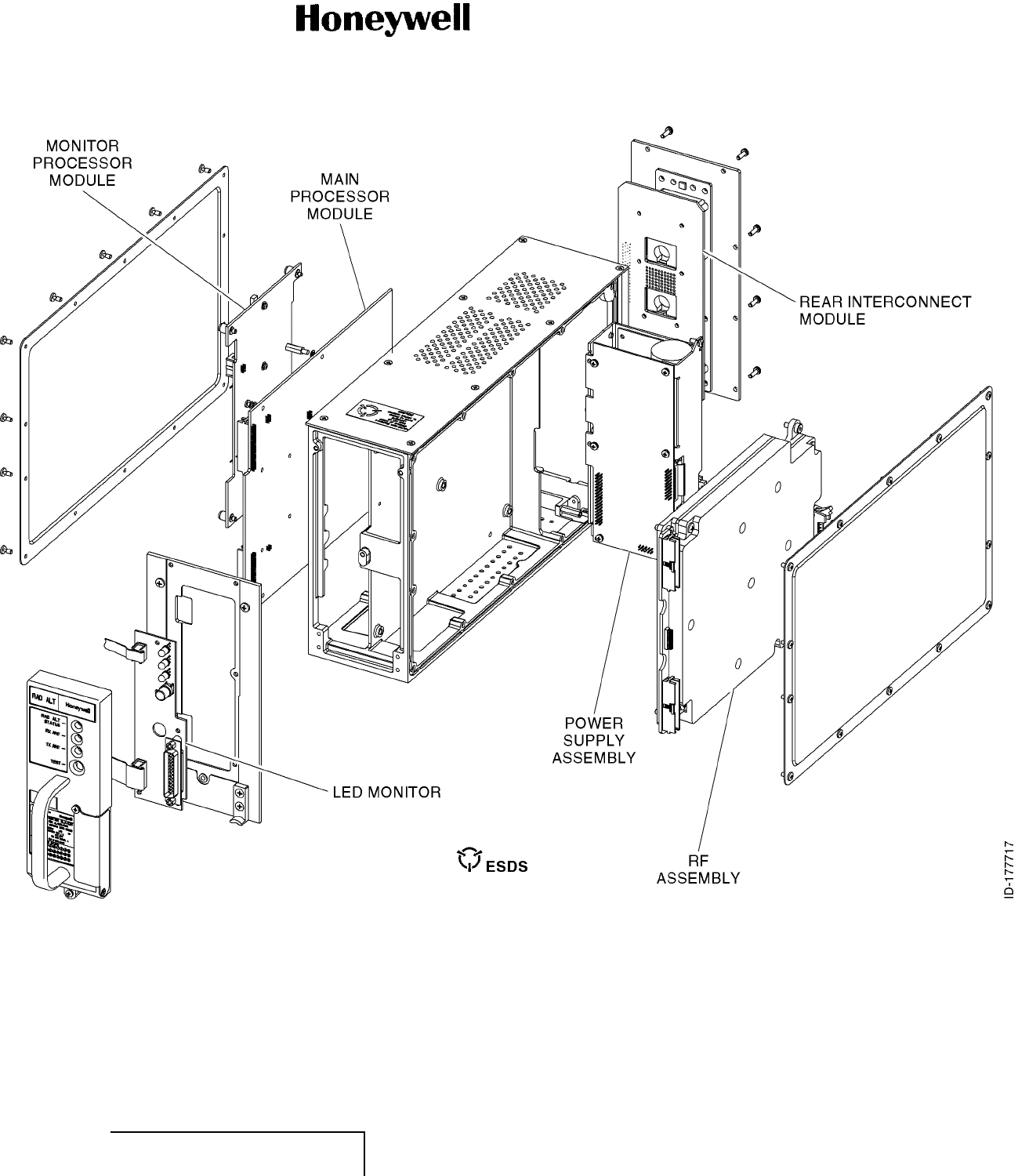
(2) Table 5 lists all modules and assemblies in the unit. Figure 2 (GRAPHIC
34-42-37-99B-803-A01) shows the location of the modules and assemblies.
Table 5. Module and Assembly Designations
Module/Board Honeywell Part
Number Reference
Series Connectors
Final Assembly 700-1796-001 --- W4,W6,W8,W11,W20,W21
• Rear Interconnect CCA 722-4667-002 1200 J1001, J1212, J1214, W2,
W23
Main Processor CCA 722-4703-002 2000 J2001, J2002, J2003, J2005
thru J2012
Power Supply Module 710-0366-001 --- ---
• Input CCA 722-4767-001 3100 P3102, W6, J3108
• Output CCA 722-4577-005 3300 J3302, P3310, P3313
Front Panel 700-1784-001
• LED CCA 722-4692-002 4000 J4001, J4002, J4003, W5, W9
Monitor Processor Module 300-90234-0502 6000 J6018, J6043, J6044, J6045
RF Assembly727-0026-001 9000 W4, W6, W7, W20, W21
• RF Module CCA 722-4656-005 9000 J9039, P9033
EFFECTIVITY
ALL 34-42-37 Page 5
10 Oct 2007
© Honeywell International Inc. Do not copy without express permission of Honeywell.

COMPONENT MAINTENANCE MANUAL
Part No. 066-50007
Blank Page
EFFECTIVITY
ALL 34-42-37 Page 6
10 Oct 2007
© Honeywell International Inc. Do not copy without express permission of Honeywell.
COMPONENT MAINTENANCE MANUAL
Part No. 066-50007
Figure 2. (Sheet 1 of 1) Module and Assembly Location (GRAPHIC 34-42-37-99B-803-A01)
EFFECTIVITY
ALL 34-42-37 Pages 7/8
10 Oct 2007
© Honeywell International Inc. Do not copy without express permission of Honeywell.
COMPONENT MAINTENANCE MANUAL
Part No. 066-50007
B. Electrical Description (Subtask 34-42-37-870-006-A01)
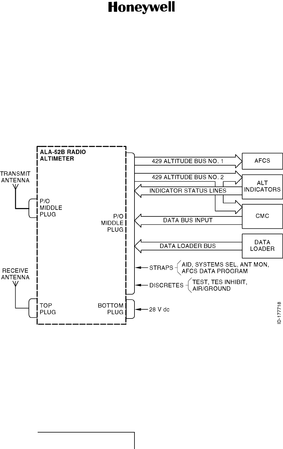
(1) Figure 3 (GRAPHIC 34-42-37-99B-804-A01) shows the ALA-52B interconnections in
the aircraft. Antenna cabling is determined by the setting of the AID strap pins in the
middle plug. The round trip delay from the ALA-52B transmitter port to the receiver port
is set to the AID value for the return signal that corresponds to a reading of zero feet.
(2) The middle plug also contains the ARINC 429 altitude bus outputs that connect to the
AFCS, cockpit altitude indicators. Data recording equipment in the form of a flash card
is available for in-flight test, though normally it is not required. For most installations,
ARINC 429 bus number 1 is connected to the Flight Management Control Computer,
and ARINC 429 bus number 2 is connected to the altitude indicators on the instrument
panel. ARINC 429 I/O is also provided for interface with the CMC.
Figure 3. (Sheet 1 of 1) ALA-52B Block Diagram (GRAPHIC 34-42-37-99B-804-A01)
(3) Besides the AID strap pins, system select strap pins are provided to designate the
installed equipment as unit number 1, 2, or 3. The antenna monitor strap pin enables
antenna monitoring, and the AFCS data program strap pins set the mode of operation
of the ARINC 429 altitude buses in case an ALA-52B failure is detected.
(4) Discretes from other systems provide test activation, the inhibiting of test, and
air/ground indication.
(5) An RS-232 port on the ALA-52B front panel (not shown) provides an attachment for a
hand-held tester for additional ramp test information, and shop test interface.
EFFECTIVITY
ALL 34-42-37 Page 9
10 Oct 2007
© Honeywell International Inc. Do not copy without express permission of Honeywell.

COMPONENT MAINTENANCE MANUAL
Part No. 066-50007
5. Theory of Operation (TASK 34-42-37-870-805-A01)
A. Overall Operation (Subtask 34-42-37-870-007-A01)
(1) The basic objective of the ALA-52B is to provide accurate height above the ground
terrain with a high degree of integrity during the approach, landing, and climb
out phases of aircraft operation. This is accomplished by transmitting a frequency
modulated continuous signal to the ground.
(2) The frequency modulation is a linear dual slope ramp. During the time required for the
transmitted signal to bounce off the ground and return to the aircraft, the transmitted
signal has changed frequency. When the transmitted signal is mixed with the return
signal bounced up from the ground, a baseband signal is produced at a frequency that
represents the difference between the transmitted and returned signal frequencies.
Since this difference frequency is proportional to the delay between the transmitted
and received signals, it is also proportional to the altitude of the aircraft.
(3) The difference frequency signal is amplified sufficiently and applied to two independent
DSPs. The amplifier gain increases with frequency to compensate for attenuation due
to increased range. The DSPs perform FFT and extract the lowest peak frequency.
This process is repeated periodically. The results are averaged and verified in the
microprocessors before being supplied to the 429 altitude data buses.
(4) The verified digital altitude information is then routed to the peripheral equipment
where it is further processed for pilot display, ground proximity warning, and AFCS
usage.
B. Block Diagram (Subtask 34-42-37-870-008-A01)
(1) RF Module
(a) The RF module, controlled by the main processor, transmits and receives the
altimeter signal. BITE circuitry is included to both test and continuously monitor
the RF module functions.
(b) The process of generating a transmission is driven by a VCO based PLL that is
controlled by a DDS. The transmitter chain supplies the receiver LO as well as
the required input for the calibration circuitry. The transmitted signal is radiated
from the transmit antenna located on the underside of the aircraft.
(c) The transmitted signal, after bouncing off the ground below the aircraft, is
collected by the receive antenna.
(d) A pair of RF switches are provided to channel the calibrated 300-foot delay
element signal through the receiver during self-test. The self-test operation
performs a full transmitter and receiver check. The self-test operation is activated
manually by the pilot or automatically when the ALA-52B is acquiring a signal.
(e) The received signal is mixed with the part of transmitted signal, producing a
difference frequency signal that is amplified and fed to an A/D converter on
the main processor module.
EFFECTIVITY
ALL 34-42-37 Page 10
10 Oct 2007
© Honeywell International Inc. Do not copy without express permission of Honeywell.

COMPONENT MAINTENANCE MANUAL
Part No. 066-50007
(2) Main Processor Module
(a) The main processor module controls the radio altimeter operation, performs
signal processing of the difference frequency and test signals, and controls the
aircraft interfaces and the data displayed on the front panel.
(b) The main processor provides all the control signals to generate an up-down linear
ramped frequency-modulated carrier wave output, determines the mode of
operation, and provides all RF control signals. It also processes the difference
frequency signals digitally. The return signal and test signals are converted to
digital data streams using an A/D converter. In addition, the main processor
module performs BITE, I/O, flash card interface, and monitor processor module
interface functions.
(c) The main processor module is divided into three major sections: the DSP section,
the 486 CPU microprocessor section, and the I/O section.
(d) When replacing the main processor module, refer to the Alignment Procedure,
in the TESTING AND FAULT ISOLATION (PGBLK 34-42-37-1000) section and
the SW Data Recording and Loading in the REPAIR (PGBLK 34-42-37-6000)
section of this manual.
1DSP Section
aThe DSP section is used to process the analog outputs from the RF
module and to generate some of the control signals to the RF module
for transmit modulation, automatic gain control, and test signals. The
difference frequency signal from the RF module is digitized using a
12-bit A/D converter. The A/D converter is also used to monitor signals
from the BITE test points on the RF module and the power supply
voltages. The digitized data from the A/D converter is stored in a FIFO
memory device which is accessed by the DSP. The DSP processes the
difference frequency and calibration frequency into altitude information.
Data is exchanged with the CPU section through a dual-port RAM,
providing maximum throughput of both processors.
2CPU Section
aThe CPU section does frame-to-frame processing of the altitude data
from the DSP section providing the resulting altitude to the I/O section.
The microprocessor in the CPU section controls all major functions
of the radio altimeter. Programmable logic devices serve as the
microprocessor controller and provide the interfaces to the memory
devices (boot routine, program, fault, and data), the data recorder/data
loader flash card, and the front panel display driver.
3I/O Section
aThe I/O section provides the two ARINC 429 altitude outputs as well as
ARINC 429 interfaces with other aircraft systems including the CMC. All
discrete inputs external to the radio altimeter are processed by the I/O
section. The I/O section also generates the external discrete outputs,
which are buffered to prevent damage to the processor circuitry. The
EFFECTIVITY
ALL 34-42-37 Page 11
10 Oct 2007
© Honeywell International Inc. Do not copy without express permission of Honeywell.

COMPONENT MAINTENANCE MANUAL
Part No. 066-50007
I/O section also contains an RS-232C production test interface. This
test interface is also used to update serial number, part number and
configuration memory as applicable, utilizing a stand-alone PTM tool
or integrated PTM tool in the Quantum Line Tester, when the main
processor module is replaced.
(3) Monitor Processor Module
(a) The monitor processor module provides a second signal processing path using a
DSP. The DSP processes the received signal and calibration signal supplied in
digital form from the Main Processor A/D converter. Also present are a clock, an
ARINC 429 receiver/selector, and static memory.
(b) The primary function of the monitor processor module is to provide the ALA-52B
with the integrity that permits Category III operations by acting as an independent
monitor for the main processor altitude computations.
(4) Power Supply Module
(a) The power supply module is a self-contained, high-efficiency, switching power
supply that converts the 28 V dc aircraft power into the required +5 V dc,+12 V
dc, and -12 V dc, operating voltages. A power-down interrupt signal provides
advanced notice of a power loss allowing the processors to temporarily retain
their status.
(5) Rear Interconnect Module
(a) The Rear Interconnect module provides interface between the ARINC connector,
the main processor, and the power supply modules. Lightning proctection for I/O
signals is provided on the Rear Interconnect.
(6) Display Data Module
(a) The display data module is mounted behind the front panel and provides an
interface to an operator through LEDs, which are visible from the front of the
ALA-52B. In addition to the LEDs, the module has a pushbutton switch and a
connector.
(b) The connector is used for testing the ALA-52B through a compatible test set or
test panel.
(7) Memory Card Interface Connector
(a) The ALA-52B ALA transceiver is provided with a connector for a PCMCIA flash
card for programming the unit at the factory or service shop.
6. Detailed Theory of Operation (TASK 34-42-37-870-806-A01)
A. General (Subtask 34-42-37-870-009-A01)
(1) See the appropriate schematic for the ALA-52B Radio Altimeter subassemblies
described in this section. All electrical signals are shown in uppercase characters.
If the signal does not contain such a suffix, then the signal is generally a dual-state
signal such as a clock or data bus.
(2) There are six subassemblies of the ALA-52B Radio Altimeter described in this
section. They are:
EFFECTIVITY
ALL 34-42-37 Page 12
10 Oct 2007
© Honeywell International Inc. Do not copy without express permission of Honeywell.

COMPONENT MAINTENANCE MANUAL
Part No. 066-50007
• RF module
• Main processor module
• Monitor processor module
• Power supply assembly
• Rear interconnect module
• Front panel module.
B. RF Module (Subtask 34-42-37-870-010-A01)
(1) General
(a) The RF module transmits and receives FM modulated C-Band signals that are
used to determine the altitude above the ground. When the transmitted signal is
mixed with the return signal bounced up from the ground, a baseband signal is
produced at a frequency that represents the difference between the transmitted
and return signal frequencies. The baseband signal frequency is directly
proportional to the altitude above the ground. This analog baseband signal is the
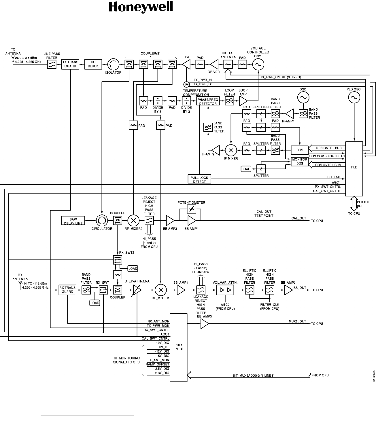
primary output from the RF Module. A simplified block diagram of the RF circuitry
is shown in Figure 4 (GRAPHIC 34-42-37-99B-805-A01)
1The transmitted signal, centered at 4.3 gigahertz with a maximum possible
span of +/-100 megahertz is radiated from the transmit antenna located
on the underside of the aircraft, and is subsequently (after bouncing off
the ground) collected by the receive antenna. A directional coupler picks
off some of the transmit signal which is mixed with the received signal,
producing a difference signal that is amplified, filtered and fed to an
analog-to-digital converter on the Main Processor module.
2BITE circuitry is also included to both test and continuously monitor the
RF module functions. A portion of the transmit signal is also fed into a
bulk acoustic wave device that provides a reflected signal calibrated to a
time delay equivalent to 300 feet (0.616usec). Cal mixer extracts a signal
corresponding to the difference frequency between transmit and delay
element signals. The difference frequency signal is fed through a multiplexer
to the A/D converter on the Main Processor board for calibration and
self-test purposes
3The PLD receives control signals from the DSP of the Processor Module and
directs them to appropriate circuitry on the RF module. A major function of
this PLD is to control the DDS which provides a nearly ideal linear frequency
sweep as a reference signal to the PLL within the transmitter chain.
EFFECTIVITY
ALL 34-42-37 Page 13
10 Oct 2007
© Honeywell International Inc. Do not copy without express permission of Honeywell.

COMPONENT MAINTENANCE MANUAL
Part No. 066-50007
Blank Page
EFFECTIVITY
ALL 34-42-37 Page 14
10 Oct 2007
© Honeywell International Inc. Do not copy without express permission of Honeywell.
COMPONENT MAINTENANCE MANUAL
Part No. 066-50007
Figure 4. (Sheet 1 of 1) RF Module Block Diagram (GRAPHIC 34-42-37-99B-805-A01)
EFFECTIVITY
ALL 34-42-37 Pages 15/16
10 Oct 2007
© Honeywell International Inc. Do not copy without express permission of Honeywell.

COMPONENT MAINTENANCE MANUAL
Part No. 066-50007
(2) Transmitter Chain
(a) The transmitter chain is driven by a VCO based PLL that is controlled by a DDS.
The transmitter chain supplies the receiver LO as well as the required input for
the calibration circuitry. The DDS is programmed by the PLD which is controlled
by the Processor Module. A second DDS, called the monitor DDS is driven with
the same frequency set-up as the main DDS in order to provide a comparison
reference to the main DDS. The lock-detect signals from the compared DDSs
and the PLL are used by the PLD to monitor the failure modes of the DDSs and
the transmitter chain.
1Reference Oscillator
aThe transistor based oscillator is powered by a 128 megahertz single
tone crystal, Y1 and amplified by a X3 multiplier, Q5 to 384 megahertz.
The 384 megahertz signal is filtered by a comb-line filter and amplified
by a gain block, U14 and filtered again before providing the clock signal
to the DDSs (U18, U32) and an LO signal to the IF mixer (U24). Two 3
decibel splitters are employed to split the signal into three outputs, two
with equal amplitude and phase at 0 dBm and one with 3 dBm. The 0
dBm signals are used to reference the DDSs(DDS1-REF, DDS2-REF).
3 dBm signal is used as IF_LO signal.
2DDS
aBoth of the DDSs (U18, U32) are driven by the PLD (U512) to generate
a frequency sweep between 82.66 megahertz to 104.88 megahertz
(approximate maximum sweep) with the external reference clock 384
megahertz. The main DDS (U32) output is feeding the IF mixer as well
as the PLD where it is compared with that from the monitor DDS.
bThe linear frequency ramp generator U32 includes an on-chip
comparator. The comparator signals are square waves. The bandwidth
is greater than 200 megahertz and has a common-mode input range of
1.3 volts to 1.8 volts. This signal helps eliminate phase noise and jitter.
cThe linear frequency ramp generator U32 output frequency range is
82.66 megahertz to 104.88 megahertz. The DDS frequency sweep
output (DDS_OUT) on U32-20 and -21 is routed through, transformer
T3, a 120 megahertz low pass filter and a 3 decibel coupler to
mixer U24. The signal from the ramp generator is mixed with the
384 megahertz IF signal so that the linear frequency modulation is
translated up in frequency to 466.66 megahertz to 488.88 megahertz.
These frequencies correspond to 4.200 gigahertz and 4.400 gigahertz
divided by 9 in the PLL circuit.
3IF Mixer:
aThe DDS_OUT signal and the IF_LO signal are routed to IF mixer U24.
The output on U24-4 has a frequency range of 466.6 megahertz –
488.8 megahertz(upper sideband). The output of U24 is routed through
an amplifier U27 and a 477 megahertz bandpass filter to PFD U33-3.
EFFECTIVITY
ALL 34-42-37 Page 17
10 Oct 2007
© Honeywell International Inc. Do not copy without express permission of Honeywell.

COMPONENT MAINTENANCE MANUAL
Part No. 066-50007
4PLL
aThe PLL consists of PFD (U33), loop filter (U28), VCO (G1), digital
attenuator(U20), preamp (U19), power amplifier (U12) and two
successive divide by 3 frequency dividers (U21, U25) for a total
frequency division by 9. The power amplifiers and the digital attenuator
are included in the PLL in order to improve the phase linearity of the
overall transmitter. The loop bandwidth is approximately 1 megahertz
which is required by the fast sweep and the desired ramp linearity. An
external PLL lock detect circuitry which is driven from the PFD U33
provides the status of the PLL to the PLD.
bThe phase-frequency detector PFD U33 is used in low noise phase
locked loop. It detects the phase/frequency difference between the
477 megahertz signal provided by the upconverted DDS signal and
the frequency divided signal derived from the 4.3 gigahertz VCO
to generate output pulses that are proportional to the phase and
frequency difference between the two signals. The reference signal
is the RF output of U24 from the 477 megahertz bandpass filter
(466.6 to 488.9 megahertz) applied to U33-3. The second signal is
the PLL_FDBK_VCO and the compliment PLL_FDBK_NVCO from
frequency divider U25. The phase-frequency detector U33 uses the
phase difference between the two signals to supply frequency up and
down pulses to comparator U28. The output of U28, a dc voltage, is
used to tune the VCO G1.
5VCO
aThe VCO G1 has a range of 4.2 to 4.4 gigahertz. The power output
is a typical 5.0dBm typical from a single supply of +3 .3 V DC. The
control voltage from U28 on G1-22 (VTUNE) increases the output
frequency of the VCO as the voltage increases. The control voltage
range is 3.5 to 7.0 V dc.
6Digital Attenuator
aThe RF output of VCO G1 is routed to digital attenuator U20-2. Digital
attenuator U20 has a range of 2.4 to 8.0 gigahertz, with an insertion
loss of less than 3.8 decibel and attenuation accuracy is ± 0.5 decibel.
The attenuator can be set between 0 to 31.5 decibels with 0.5 decibel
steps. Six control voltage inputs, switch between 0 and +3 to +5 V dc,
are used to select each attenuation state. The digital attenuator U20 is
controlled by the PLD U512 for dynamic power control that is required
for board to board variation and temperature variation.
7Driver Amp, Power Amp and Power Detector
aThe RF output of Digital Attenuator U20-2 is connected to driver
amplifier U19-3. The driver amplifier U20 provides about 20 decibels
of gain and the PA U12 27 decibels of gain. Both operate with 5 volt
supply and consume about 130 mA and 600 mA respectively. The PA
provides an internal power detector which uses an external temperature
EFFECTIVITY
ALL 34-42-37 Page 18
10 Oct 2007
© Honeywell International Inc. Do not copy without express permission of Honeywell.

COMPONENT MAINTENANCE MANUAL
Part No. 066-50007
compensation circuitry. The temperature compensated circuit drives
two comparators whose output is sent to PLD U512, which in turn
control the digital attenuator to control the power. The temperature
compensated detector enables the power to be controlled within +/-1
decibel over the operating temperature range. PA U12 is capable of
deliveringupto29dBmpower.
8Couplers
aThe RF output of the power amplifier U12 is on U12-12. The output is
routed through three 23-decibel couplers and one 33-decibel coupler.
The three 23 decibel coupled signals are used for Receive Mixer LO
U12, Cal Mixer LO U11 and for calibration signal generation using BAW
device U6. 33 decibel coupler is used to sample the output signal
and feed back to the PFD U33 through frequency dividers U21 &
U25. There exist two more 23 decibel couplers for test signal injection
before LNA, U7.
bEach directional coupler consists of two microstrip coupled lines with a
gap dimension of which depends on the coupling requirements. The
coupling length is quarter wavelength and one port of each directional
coupler is terminated by 50 ohm shielded resistors (R10, R36, R88,
R89, R90, R121). The printed structure of coupler provides 0.25
decibel maximum loss.
9Isolator
aAn isolator, U17 is placed between the Power Amplifier and the
Transmit antenna to minimize reflections from the transmit antenna
and associated cables and connectors and improve the VSWR. This
is a SMT device and provides 20 decibel minimum isolation with 0.5
decibel of maximum insertion loss.
10Low-Pass Filter
aA printed microstrip low pass filter is employed to attenuate the
harmonics up to 18 gigahertz. This filter provides 30 decibel and
15 decibel for 2nd and 3rd harmonics respectively and a maximum
insertion loss of 0.25 decibel. The return loss of this filter is better
than 18 decibel. The output of the low-pass filter is routed to transmit
antenna connector J1004-1.
11DC block and the Transguards
aA high-voltage matched capacitor circuitry and transguard are used
in the transmitter chain to provide protection transmitter amplifier and
the DC antenna monitoring circuit from voltage transients which are
caused by lightning.
12RF FPGA
aThe FPGA supports a 24 bit serial interface between the DSP and
RF module. The DSP uses the DATA_IN and DATA_CLK signals to
transfer 24 bit serial data sequences to the FPGA that provide it with
EFFECTIVITY
ALL 34-42-37 Page 19
10 Oct 2007
© Honeywell International Inc. Do not copy without express permission of Honeywell.

COMPONENT MAINTENANCE MANUAL
Part No. 066-50007
system select information, control the U1 Receive RF switch with the
RX_SWT_CTRL signal, control the U3 Calibration RF switch with
the CAL_SWT_CTRL signal and control power to the U7 LNA with
the RF_AGC signal. The FPGA returns received DATA_IN data on
the DATA_OUT line when RDATA_EN is low and the FSYNC signal
when RDATA_EN is high.
bThe FPGA generates the FSYNC and DOWN_UP signals based on the
system select information provided by the 24 bit serial interface. The
frequency of the DOWN_UP signal is 145 Hz for system select 1, 150
Hz for system select 2 and 155 Hz for system select 3. The FSYNC
frequencies are one-half the DOWN_UP frequencies. Assertion of
the RAMP_CLR signal cause the FSYNC and DOWN_UP signals to
be held low.
cThe FPGA gets ramp rate information by reading ADC U510 using the
A2D_CS, A2D_SCLK and A2D_DOUT signals. The ADC input is
the DAC12_0 signal and its voltage is proportional to the ramp rate
required by the DSP.
dThe FPGA programs the main DDS U32 using the DDS1_CS,
DDS1_SDIO and DDS1_SCLK signals. The DDS1_SDO signal
provides the FPGA readback capability of the DDS internal registers.
Signals DDS1_RESET and DDS1_IOSYNC are used to reset the DDS.
Similar signals support the monitor DDS U18.
eBoth DDS are programmed with identical ramp information based on
system select and the ramp rate information from the ADC. For system
select 1 the DDS are programmed such that the lower transmitter
frequency is held constant at 4.235 gigahertz, for system select 2 the
upper transmitter frequency is held constant at 4.365 gigahertz and
for system select 3 the transmitter frequency range is held centered
at 4.3 gigahertz.
fThe FPGA FUD signal is used to initially program the DDS for a single
4.3 gigahertz transmitter frequency. During normal operation the FPGA
PS0 signal is then used to program the DDS registers with new ramp
rate and frequency range data. The PS0 signal also controls the ramp
frequency direction of the DDS.
gThe FPGA uses the TX_PWR_DET_LO and TX_PWR_DET_HI
signals from comparator U514 to level the transmitter power. The
FPGA periodically adjusts the TX_.5dB_CTRL to TX_16dB_CTRL
signal lines in .5 decibel steps until both TX_PWR_DET_LO and
TX_PWR_DET_HI signals are high.
hThe FPGA provides limited fault detection reporting to the main
processor module via the FAULT_EB and FAULT_EF signals. Via the
bite fault multiplexer U4 when the tri-state FAULT_EB signal is pulled
low the LRU will generate an EB fault and similarly polarity changes in
FAULT_EF signal will cause the LRU to report an EF fault. Only when
EFFECTIVITY
ALL 34-42-37 Page 20
10 Oct 2007
© Honeywell International Inc. Do not copy without express permission of Honeywell.

COMPONENT MAINTENANCE MANUAL
Part No. 066-50007
the RF_AGC signals at FPGA pins 27 and 24 miss-compare will the
EF fault be generated. Transmitter leveling faults, miss-compare faults
between the two DDS outputs, 384 megahertz clock frequency or
20 megahertz clock frequency(G500) accuracy faults, or transmitter
PLL loop faults occurring when the PLL_LOCK_DET signal goes low
cause the EB fault to be generated.
(3) Receiver Chain
(a) The heart of the receiver chain is the double balanced mixer. The signal received
from the Rx Antenna is mixed with a sample of the transmitter signal to produce a
low frequency signal that is proportional to the altitude to the ground. An LNA
with bypass switch is employed to adjust the LNA gain between the two states as
required by the received signal amplitude.
1DC block and Receive Transguards
aThe BPF provides the required dc block for the receiver chain while the
transguard provides protection for the antenna monitoring circuit from
voltage tansients which are caused by lightning.
2Bandpass Filter
aThe receiver input is from RX antenna connector J1005-1. The receive
RF signal from the antenna is routed through a 4.3 gigahertz bandpass
filter. This printed bandpass filter uses parallel coupled, half-wave
long microstrip resonators, coupled along half of their length with the
adjacent resonators. The seven-resonator bandpass filter provides
2.5 decibel loss in the bandpass and 50 decibel attenuation for the
multilayer spiral parasitic signal at 5.03 gigahertz and overall out of
band attenuation to reject out of band HIRF up to 18 gigahertz.
3Receive/Calibration switches
aThe output of the bandpass filter is routed to the LNA through the
RF switch U1. The RF switch U1 is a broadband high isolation,
non-reflective SPDT. The receiver and calibration switches (U1 and
U3) provide the facility to channel the approprate signal through the
receiver chain and are used for the self-test and noise floor test. The
switches are non-reflective, high isolation switches and provides about
50 decibel of isolation at 4.3 gigahertz with 1.5 decibel insertion loss.
The high isolation on the PCB is achieved through co-planner wave
guide design instead of microstrip.
bThe RF switch operates with complementary negative control voltage
logic of -5 to 0 V dc and does not need bias supply. Control signals
are generated by the PLD through CMOS level shifters (U2) since
the PLD operates with 3.3volts. The switch control voltages are also
being monitored by the MUX U4.
cThe control of the RF switch is by the control signals on U1-15 and
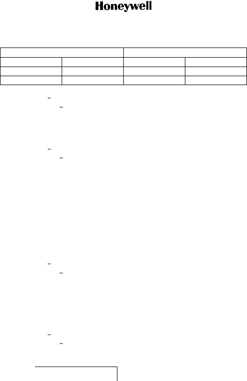
-16. Refer to Table 6 for the U1 control truth table. The RF1 output is
not used and grounded through resistor R5.
EFFECTIVITY
ALL 34-42-37 Page 21
10 Oct 2007
© Honeywell International Inc. Do not copy without express permission of Honeywell.
COMPONENT MAINTENANCE MANUAL
Part No. 066-50007
Table6. U1ControlTruthTable
Control Input Signal Path State
U1-16 (A) U1-15 (B) RFC to RF1 RFC to RF2
High Low On Off
Low High Off On
4Low Noise Amplifier/Step Attenuator
aThe receiver front-end C-Band low noise amplifier, U7 has a typical
noise figure of 1.8 decibel and provides 12 decibel of gain for lower level
signals (high altitudes), and 6 decibel attenuation (total loss 18 decibel)
for the higher level signals (low altitudes). The amplifier is under the
binary control of the PLD U512. The low noise amplifier insures with
minimum noise figure for signals received at high altitudes.
5RX Mixer
aThe receive mixer (U10) is a double balanced mixer with built-in LO
amplifier and work with +2 dBm of typical LO signal. This provides
8 decibels of conversion loss, 32 decibels LO/RF isolation, and 25
decibels LO/IF isolation. In the receive path, the RF signal on U10-8 is
from the Rx antenna through the RF Switch U1. The LO signal to U10-1
is from the 23 decibels coupler on the output of the power amplifier
U12-12. The two signals are mixed to provide the IF baseband signal
(IF_TO_BB) on U10-5.
(4) Cal Signal Chain
(a) A directional coupler picks off some of the transmitter signal and feeds it to a
bulk acoustic wave device that provides a reflected signal calibrated to a time
delay equivalent to 300 feet (0.616usec). Calibration mixer extracts a signal at
the difference frequency between transmit and delay element signals. The
output is filtered and amplified and processed by the CPU for calibration and
self-test purposes.
1Delay-Line
aThe 300-foot Bulk acoustic wave SMT delay line U6 with 0.603 to
0.616 usec delay consists of a cylindrical rod of quartz crystal for
the propagation of an acoustic wave. This one- port delay line uses
only one transducer for both input and output and therefore we have
included a circulator that properly directs the input to the BAW and
output of the delayed signal to the calibration mixer. The circulator
prevents the transmitter sample signal from directly being applied to the
calibration mixer. The BAW delayed signal incurs 28 to 38 decibels of
insertion loss at 4.3 gigahertz.
2Circulator
aThe circulator, U5 is a counterclockwise SMT device and provides 22
decibels minimum isolation at 0.5 decibels maximum insertion loss. A
EFFECTIVITY
ALL 34-42-37 Page 22
10 Oct 2007
© Honeywell International Inc. Do not copy without express permission of Honeywell.

COMPONENT MAINTENANCE MANUAL
Part No. 066-50007
portion of the transmit signal is supplied to port-1, which in turn feeds
the delay-line at port-2 to produce the delayed signal. The reflected
signal is extracted from port-3 and fed to the cal mixer.
3Calibration Mixer
aThe device used for calibration mixer U11 is the same as receive
mixer U10. In the calibration path, the RF signal on U11-8 is from the
circulator U5 output. The LO signal, CAL_LO_MIX on U11-1 is from
the 23 decibels coupler on the output of the power amplifier U12-12.
The two signals are mixed to supply the IF calibration baseband signal
(CAL_TO_BB) on U11-5.
(5) IF Sections
(a) U506, U507, and U505 are the calibration output amplifier chain. U506 acts as a
selectable high-pass filter controlled by HI_PASS1 and HI_PASS2 signals which
comes from the DSP. In the case of the calibration signal, it allows for increased
high pass filtering in the response to the calibration IF. With switch 2 (S2) of U506
open, C532 is not part of the circuit and the high pass response is determined by
C533. With S2 closed, C532 is then in parallel with C533 and is the dominant
factor in determining the response of the input stage of the filter.
(b) The input signal CAL_TO_BB goes through C533, which gives it a high-pass
response. The signal then goes into U507 which is a non-inverting amplifier
withagainof20.
(c) The output of U507 goes to C534 which produces a high-pass response. This is
also selectable by HI_PASS2. With switch 4 (S4) of U506 open, R66 is not part of
the circuit and the response is determined by C534 and R536. With S4 closed,
the response is determined by C534 and the parallel combination of R536 and
R66 to determine the cutoff frequencies/response. The output goes to U504,
which is an inverting amplifier with a gain of 2. This gain can be adjusted using
the pot R34. Next, the output goes through C512 for high-pass filtering and
becomes CAL_OUT, which goes to the differential amplifiers in the DSP section.
(d) The IF input signal IF_TO_BB is ac coupled to transistor Q1, which is a common
emitter amplifier. The output from the collector of Q1 is filtered by C36 (low-pass)
and C528 (high-pass) and then it is applied to high-pass amplifier U505. Overall,
Q1 and U505 have 30 decibels of gain and low noise. The output of U505 goes
through R533 and then into a selectable high-pass filters which is determined
by HI_PASS1 and U506. With switch 1 (S1) and U505 open, C45 is not part of
the circuit and the response is determined by C531 and the input impedance
of U502 which is 100-ohms. With S1 closed, C45 is in parallel with C531 and
becomes the dominant capacitor for the response. The response is essentially
C45 and 100 ohms. The output of the high-pass filter goes to U502-A, which is
a 40 decibels gain voltage controlled amplifier. It is controlled by the IF_AGC
which comes in on pin 28 of J21. The voltage at pin 16 of U502-A and pin 9
of U502-B varies from 0 to 2.5 volts.
(e) The gain of U502 can varied from 0 decibel gain to 40 decibels gain. The output
of U502-A goes through a high-pass filter (C505) and then it is routed to the pin
EFFECTIVITY
ALL 34-42-37 Page 23
10 Oct 2007
© Honeywell International Inc. Do not copy without express permission of Honeywell.

COMPONENT MAINTENANCE MANUAL
Part No. 066-50007
7 of U502-B. U502-B is a 0 to 40 decibels voltage controlled amplifier. Its gain
goes from 0 to 40 decibels gain when the input on pin 9 goes from 1.25 to
2.5 volts. Overall, from pin 2 of U502-A to pin 11 of U502-B, there is up to 80
decibels gain available depends up on the IF_AGC control signal. The output is
low-pass filtered through R503 and C503 and goes into the first of two switched
capacitor filters.
(f) U500 and U501 are switched capacitor elliptical filters which have a response
equivalent to an eight-pole elliptical filter. The cutoff is determined by the
FILTER_CLK which comes from the DSP section. The cutoff is at 43 KHz. The
output of these filters have an uncommitted op-amp with which resistors R1, R2,
R3, and capacitors C1 and C2, are a dual, two-pole low-pass filter to reduce
the amount of clock noise on the output. The output of U500 is connected to
U501, which is essentially the same circuit, to give it a very sharp cut-off to
prevent high frequencies going to the DSP. The output at pin 5 of U501 goes
through high-pass filter C507 to pin 3 of amplifier U503 which has a gain of 15
decibels. The output of U503 goes through R22 and is the BASEBAND_OUT
which goes to the DSP section.
(6) BITE MUX
(a) The BITE MUX U4 is a CMOS latched 16-bit to 1 analog multiplexer. The BITE
MUX has different voltages on its inputs which are monitored by the DSP section.
On input 1 (S1) and 2 (S2), 2.5V and 3.3 volts going to the RF section are
monitored. Also, input 2 (S2) provides FAULT_EB signal which can be decoded to
a set of RF circuitry failures. Inputs 3 (S3) thru 4 (S8) are the RX_SWT_CNTRL
signal voltage which is monitored. Input 7 (S7) is the FAULT_EF signal voltage
which is monitored. Input 7 (S6) is the CAL_SWT_CNTRL signal voltage which is
monitored. Input 8 (S8) is the RF_AGC signal voltage which is monitored. Input 9
(S9) is the +12_DIG volts which is monitored. Input 10 (S10) is the +5V_RF which
is monitored. Input 11 (S11) is the -12_DIG volts which is monitored. Input 12
(S12) is the -5_DIG volts which is monitored. Input 13 (S13) is the TX_ANT_MON
which is monitored and should look like a short when connected to an antenna.
Input 14 (S14) is the RX_ANT_MON which is monitored and should look like
a short if its connected. Input 15 (S15) is the RAMP_OFFSET signal voltage
which is monitored. Input 16 (S16) is the TX_POWER_MON which is monitored.
U508-A is a buffer amplifier to buffer the output going to the DSP section.
(7) Power Supply Filtering
(a) The power supply filtering consists of L507, L501, L505, and L504. RF CCA
contains voltage regulators U13, U16, U22, U23, U29, U30, U34, U509 &
U515 linear regulators to generate a clean +1.8V, +2.5V, +3.3V, +5.0V, +10V,
and -5V for various RF and Digital ICs. U5 is switching regulator to convert
12V to +6V DC with 85 percent efficiency. This device contains internal short
circuit protection also.
EFFECTIVITY
ALL 34-42-37 Page 24
10 Oct 2007
© Honeywell International Inc. Do not copy without express permission of Honeywell.

COMPONENT MAINTENANCE MANUAL
Part No. 066-50007
C. Main Processor Module (Subtask 34-42-37-870-011-A01)
(1) General
(a) See Figure 2004 (GRAPHIC 34-42-37-99B-814-A01) for a schematic diagram on
the Main Processor Module.
(b) The main processor module:
• Controls the radio altimeter operation
• Does signal processing of the difference frequency and test signals
• Controls the aircraft interfaces and the data displayed on the front panel.
(c) The main processor module is divided into three major sections:
• 486 microprocessor section
• I/O section
• DSP section.
(2) 486 Microprocessor Section
(a) General
1The 486 microprocessor section (CPU section) does frame-to-frame
processing of the altitude data from the DSP section and supplies the
altitude to the I/O section. Programmable logic devices serve as the
microprocessor controllers and are the interfaces to:
• Memory devices (boot routine, program, fault, and data
• Data recorder/data loader flash card
• Front panel display driver.
2The microprocessor U39, in the CPU section, controls all major functions of
the radio altimeter. Microprocessor U39 is an Intel®486 SX microprocessor,
which does not have a math coprocessor. The CLK signal on U39-123
is the fundamental timer and the internal operational frequency for the
microprocessor.
3Address lines A31 thru A2, together with the byte enables BE0* thru BE3*,
define the physical area of memory or I/O space accessed. Address lines
A31 thru A4 (2) are used to drive addresses into the microprocessor to do
cache line validations. Address lines A31 thru A2 are not driven during bus
or address hold. The byte enable signals BE0* thru BE3* indicate active
bytes during read and write cycles.
4On the first cycle of a cache fill, the external system assumes that all byte
enables are active. Data lines D31 thru D0 are the data lines for the
microprocessor U39. Data lines D0 thru D7 define the least significant byte
of the data bus while lines D24 thru D31 define the most significant byte of
the data bus. Data parity pins DP0 thru DP3 are connected to VCC through
pull-up resistors because the system does not use parity.
EFFECTIVITY
ALL 34-42-37 Page 25
10 Oct 2007
© Honeywell International Inc. Do not copy without express permission of Honeywell.

COMPONENT MAINTENANCE MANUAL
Part No. 066-50007
5A temperature sensor is used for the data log for temperature. It is for BIT
and is used to log the temperature when a failure happens. This is used
in debug.
(b) Microprocessor Control
1Programmable logic device U52 and integrated peripheral controller U22
are the heart of the Main Processor CCA. The bus controller U52 has
all the logic signals and timing needed to do chip selects and control
microprocessor U39. Oscillator Y1 is a 24 megahertz clock, which is divided
by 2. This supplies 12 megahertz to microprocessor U39. The 24 megahertz
is used because there are two edges used to control the timing.
2The 5-volt monitor and watchdog timer U28 reset gives over and under
voltage protection. It is set for about 5 to 7 percent of the upper 5 volts,
which is needed for the microprocessor U39. When the voltage falls below
4.75 volts or rises above 5.25 volts, the reset happens and holds the
microprocessor in reset.
3Crystal G2, on integrated peripheral controller U22-72, is a 32.768 kilohertz
crystal. It is used to control the real time clock for the software. It also
controls timing and tagging information.
(c) Microprocessor Memory
1Data RAMs U40, U47, U53 and U61 are 128K X 32 CMOS static RAMs.
The data RAMs are backed up by +5 Volts for 20 seconds, which decreases
power-up time. The chip select, on pin 22 of each device, is used to make
sure there are no inadvertent writes to each RAM. The chip selects are held
high to disable the RAM as the power goes down. This makes sure that no
exterior writes happen to the RAM.
2Flash memories U16, U17, U25, and U26, are used to store the program.
These memories are read/write and can be rewritten as long as 12 volts is
applied to the device. The flash memories 12-volt switch circuit consists of
transistor Q6 and the associated components. The flash memories 12-volt
switch is controlled to make sure that no inadvertent writes happen during
operation. It is a switch needed to turn on the 12 Volts to the flash memory.
3Devices U2, U3, U9 and U10 are the byte swapping logic. There are two
independent buses to accommodate 32-bit and 16/8 bit devices. The FAST
32-bit bus only talks with the program/data memories. The SLOW bus talks
to all other I/O peripherals. For the 32-bit microprocessor U39 to talk to any
8- or 16-bit devices, the 16- and 8-bit memories need external byte swapping
logic to route data to the appropriate data lines. Separate buses distribute
capacitance loading and thus lower signal noise.
4Devices U4, U11 and U60 are address buffers. Half of U11 is used to buffer
other signals for increased drive and to make sure that the signals are clean
going to other sections of the module. Address buffer U60 is the control
signals buffer, which is all the signals that go to either the I/O section or the
DSP section. The signals are pulled up to make sure that no noise gets
on the line and inadvertently actuates the signal.
EFFECTIVITY
ALL 34-42-37 Page 26
10 Oct 2007
© Honeywell International Inc. Do not copy without express permission of Honeywell.

COMPONENT MAINTENANCE MANUAL
Part No. 066-50007
5The D flip-flops U42 and U48 are used in the I/O discretes circuit. On
U48, the FLASH_WR_ENABLE discrete is used to switch 12 volts. The
DSP_RESET discrete and RS232_RST discrete are used on two different
peripherals. Another discrete is the LCD_LITE_EN, which turns on the
backlight on a plug-in test display. Device U42 makes up the input discretes,
which monitor various inputs from the data card and some of the test buttons
from the front panel.
6Device U59 is a 32K byte CMOS EEPROM. This is the storage site for
configuration memory and fault memory recorded during the flight legs.
7The BOOT block flash memory U50 is where microprocessor U39 gets
the start-up information and power up. Device U50 is a 128K X 8 flash
memory and a switch. The switch has two settings: SHOP_MODE and
NORMAL_MODE. The flash memories are not preprogrammed.
• In the SHOP_MODE, the switch lets 12 volts access the BOOT block
section. This is done so that in flight (even if the 12 volts is inadvertently
turned on) the BOOT code can not be overridden. It can only be done in
the shop and the unit has to be open.
• In the NORMAL_MODE, part of the BOOT code can be overridden but
that is not essential to the unit so memory cannot be lost.
8A UART U65 does parallel-to-serial conversion on data characters received
from the microprocessor. The microprocessor can read the complete status
of the UART U65 at any time during the functional operation. When CS0
and CS1 are high and CS2 is low, the chip is selected. This enables
communication between the UART and the microprocessor.
9When the interrupt output pin U65-33 goes high when any one of the
following interrupt types has an active high condition and is enabled through
the interupt enable register:
• Receiver Line Status
• Received Data Available
• Transmitter Holding Register Empty
• MODEM Status.
10The INTR signal is reset low upon the appropriate interrupt service or
a master reset operation.
11Connector J8 is the 34-pin power supply connector. The +24, +5, +12, and
-12 volts have filter capacitors and inductors. The PWRDN_INT* signal
on J8-4 is buffered by two Schmitt trigger inverters and a pull-up resistor
and capacitor. This is the power supply signal that tells the unit that the
200 milliseconds power hold-up is about to go down, and to store all the
information before all power is lost.
12Connector J12 is the in-circuit programmable connector. This connector
is used to program microprocessor U52 and U70, the circuit card PLDs.
EFFECTIVITY
ALL 34-42-37 Page 27
10 Oct 2007
© Honeywell International Inc. Do not copy without express permission of Honeywell.

COMPONENT MAINTENANCE MANUAL
Part No. 066-50007
Microprocessor U52 and U70 can be reprogrammed as many times as
needed.
(3) I/O Section
(a) General
1The I/O section of the Main Processor Module supplies the necessary signal
level conversion, bipolar to TTL and TTL to bipolar. The I/O section also
does the serial to parallel and parallel to serial conversion needed to transfer
ARINC 429 and discrete input/output information between the I/O module
and the main processor data bus.
(b) ARINC 429 Inputs
1The ARINC 429 receivers 1 and 2 are in U20. The ARINC 429 receivers
3 and 4 are in U27. The ARINC 429 receivers 1, 2, 3 and 4 are dual 429
receivers used to convert the bipolar input signals from standard 429 levels
(+12 to -12 V dc) to standard TTL levels (0 to +5 V dc) needed for proper
operation.
2There are four ARINC 429 inputs to ARINC 429 receivers 1 and 2, U20.
They are:
• FREQ_FUN_SEL INPUT_PORTA_A (J6-41)
• FREQ_FUN_SEL INPUT_PORTA_B (J6-42)
• FREQ_FUN_SEL INPUT_PORTB_A (J6-49)
• FREQ_FUN_SEL INPUT_PORTB_B (J6-50).
3The TTL level serial data output from U20-5, -8, -12, -15 dual receiver U20 is
applied to XCVR LSI U49-19, -20, -21, -22. The serial data is shifted into
internal registers and stored as 8-bit parallel bytes. When a valid word is
received, a processor interrupt IOINT signal is asserted at U49-27.
4The microprocessor U39 responds to this interrupt by the addresses SA2
and SA3 on U49-6 and -7. Signal IOCS1 on U49-5 is asserted low. The
W/R SA4 signal on U49-2 is asserted high. This selects U49 and the data
byte is placed onto the IO_DATA bus (D0-D7) The D0-D7 I/O data bus lines
are applied to the lower section of bidirectional 429 data buffer U37, which
interfaces XCVR LSI U49 to the microprocessor slow data bus.
5The ARINC 429 receivers 3 and 4 operate the same as the ARINC 429
receivers 1 and 2 and are not described.
(c) ARINC 429 Outputs
1There are two ARINC transmitters on the Main Processor CCA. ARINC
429 transmitter 1 is U66. ARINC 429 transmitter 2 is U67. The outputs
of transmitter 1 are CMC_OUTPUT_A and on CMC_OUTPUT _B on
J6-61 and -62. The outputs of transmitter 2 are 429_OUTPUT _#0_A and
429_OUTPUT _#0_B on J6-55 and -56. Because 429 signal processing is
identical for both outputs, only transmitter 1, U66, is described.
EFFECTIVITY
ALL 34-42-37 Page 28
10 Oct 2007
© Honeywell International Inc. Do not copy without express permission of Honeywell.

COMPONENT MAINTENANCE MANUAL
Part No. 066-50007
2To transmit, the main processor places a data byte on the I/O data bus
through bidirectional 429 data buffer U37. Bidirectional 429 data buffer U37
addresses and selects 429 LSI #1 U49 and asserts WR low. The data byte
present at the data inputs to U37, is clocked out as a serial TTL level data bit
stream from LSI#1 U49-3 and -4. The serial data steam is applied to ARINC
429 transmitter U66-6 and -23. Transmitter U66 converts the TTL input to a
bipolar output at U66-13 and -17. The bipolar output from U66 is routed
through J6-61 and -62 to the rear interconnect board.
3The bipolar output from U66-13 and -17 is also routed through multiplexer
U56 and fed back as 429_BITE_INPUT_A and 429_BITE_INPUT_B to 429
receiver U27-4 and -6. The signal is converted to TTL levels and applied
to LSI U49-25 and -26.This allows the main processor to read and verify
the transmitted data.
(d) Discrete Inputs
1The 16 discrete inputs from the rear interconnect module are applied to the
main processor module at pins 15 thru 30 of connector J6. Eight of the 16
input lines are applied to the inputs of discrete input latch U38 through
diode networks and resistor divider network R36. The other eight lines are
applied to discrete input latch U38 through diode network and resistor
divider network RR27. The outputs from discrete input latch U38 are placed
directly on the microprocessor slow data bus.
2Resistor divider networks R27 and R36 lower the bipolar level signals to TTL
levels. The diode networks supply over-voltage protection for the U38 inputs.
(e) Discrete Outputs
1Discrete output data is placed on the microprocessor slow data bus and
applied discrete output/429 TX setup latch U69. The data is latched and
transferred to the 1Q and 2Q outputs of U69. The control signals TX1EN
and IOCS5 at U69-25 and -48 are asserted. The 1Q outputs of U69 are
used as strobe and sync pulses to select 429 transmitters 1 thru 4 on
the I/O control bus.
2The 2Q outputs are the discrete data lines, which are applied to power
driver U32. The 2Q outputs from power driver U32 are unregulated 24-volt
signal levels that are transmitted to the rear interconnect module through
connector J6.
(f) Shut Down Logic
1Two discrete are present on the rear connector, but are not connected
internally. The unit is strapped for interrupt mode. One discrete is strapped
high the other discrete is strapped low. In the interrupt mode the high
and low discrete is applied through a diode network and resistor divider
network R27 to the A and B sections of logic gate U68 where it is inverted
to produce a high INT_ENABLE signal on I/O control bus. Logic gate U68
inverts the high signal back to its original low status before it is latched into
discrete input latch U38.
EFFECTIVITY
ALL 34-42-37 Page 29
10 Oct 2007
© Honeywell International Inc. Do not copy without express permission of Honeywell.

COMPONENT MAINTENANCE MANUAL
Part No. 066-50007
2The high INT_ENABLE signal on I/O control bus is applied to the C and D
sections of U68. The outputs of U68C and U68D are determined by the state
of the MON1 and MON2 signals at pins 9 and 12. In normal operational
conditions (no failures or errors detected), the MON1 and MON2 lines are
low, and do not affect the operation of 429 transmitters U66 and U67.
3If a failure is detected, the monitor processor may assert a high MON1 or a
high MON2 signal, which produces a low output from U68C or U68D. These
low outputs are applied to the CLOCK (pin 25) and SYNC (pin 4) inputs of
429 TX #1 U66 and 429 TX #2 U67 to shut down the transmitters.
(4) DSP Section
(a) General
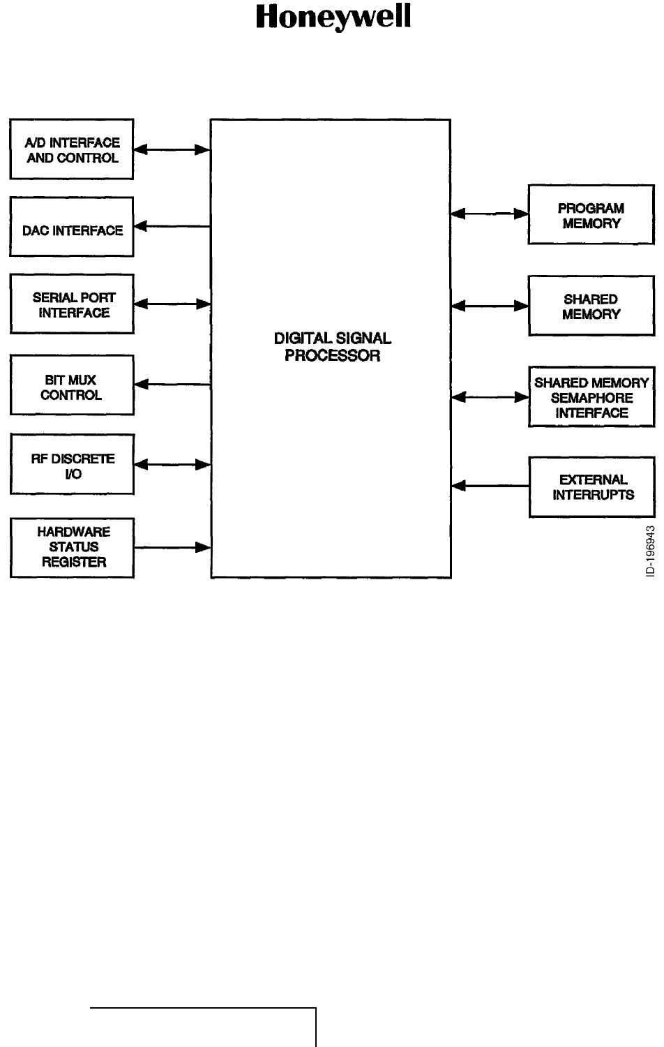
1See Figure 5 (GRAPHIC 34-42-37-99B-806-A01) for a block diagram of the
DSP section. The DSP section is used to process the analog outputs
from the RF module. The DSP section also generates some of the control
signals to the RF module for:
• Transmit modulation
• Automatic gain control
• Test signals.
(b) Analog Input Circuits
1The baseband signal (DETRX1), which is the output from the RF on the RF
control module, goes into differential amplifier U45A. Differential amplifier
U45A buffers the output that goes to analog MUX U46-6. Differential
amplifier U45B is another buffer on the same signal, which buffers the signal
that goes to the monitor processor.
2Differential amplifier U36A buffers the calibration output signal (DETRX2
from the RF control module. It buffers the signal going into analog MUX
U46-7. Another differential amplifier is U36B, which buffers the calibration
output signal goes to the monitor processor.
3Multiplexer U46 is a CMOS latched eight channels-to-one analog multiplexer.
It switches between the calibration output signal and the baseband signal
or any of the other inputs. In normal operation U46 alternately samples
the calibration output signal and the baseband signal. The output of U46
goes to U57, which is a 12-bit A/D converter. Converter U57 output is
controlled by the MUX addresses 0 thru 2, which are generated by the DSP
I/O controller U70.
(c) Analog to Digital Conversion Circuits
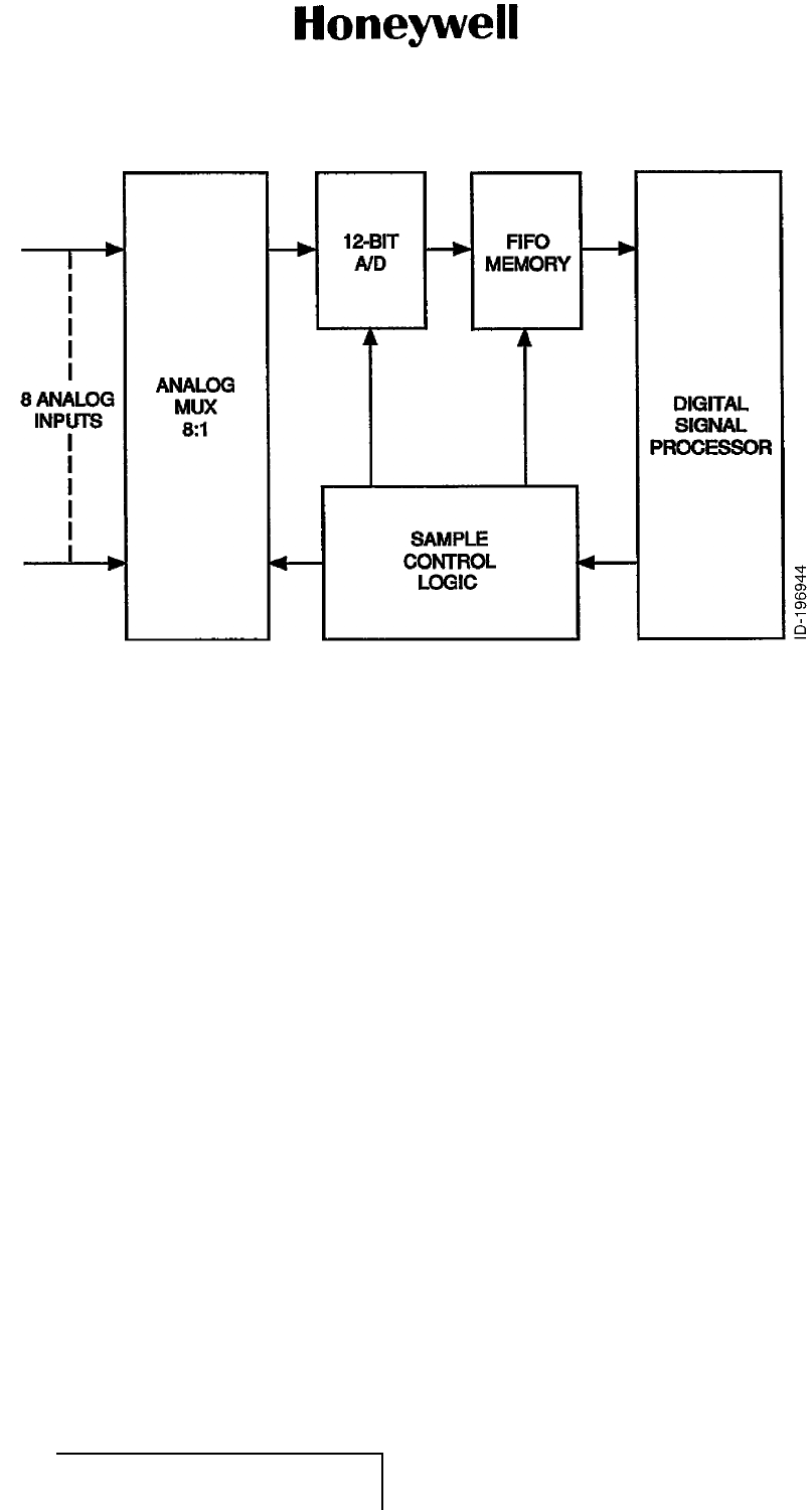
1See Figure 6 (GRAPHIC 34-42-37-99B-807-A01) for a block diagram of the
DSP section. The analog signals from the RF module are digitized in 12-bit
A/D converter U57. The A/D converter is also used to monitor signals from
the BITE test points on the RF module and the power supply voltages. The
digitized data from the A/D converter is stored in FIFO memory devices U18
and U29, which are accessed by the DSP. The output of the FIFOs goes
EFFECTIVITY
ALL 34-42-37 Page 30
10 Oct 2007
© Honeywell International Inc. Do not copy without express permission of Honeywell.

COMPONENT MAINTENANCE MANUAL
Part No. 066-50007
to the DSP_DATA [31:0] bus where the microprocessor has access to
the contents of the FIFO.
2Another mode of operation is byte sampling. The microprocessor determines
that it wants to look at either the RX_MUX on J10/J2-20 from the RF control
module or the bit MUX U43. This allows the microprocessor to monitor
different voltages. The BIT output has a MUX on the RF control module,
which allows the microprocessor to monitor RF test points.
3The BIT MUX U43 enables a monitor of the power supply voltages +24,
+12, and -12 and also a loop back DAC output (DAC8_0). Inputs DSPBD0,
1 and 2 are used to determine which one of the inputs is monitored. The
DSP U15 writes to a latch inside the MUX U43 to select which of the 8
inputs it is going to look at.
(d) DSP Memory Circuits
1The output of the FIFOs U18 and U29 is accessed by U15, which is the DSP.
The DSP processes the difference frequency and calibration frequency into
altitude information
2Memory devices U6, U7, U12, and U23 are 32 k X 8 SRAMs, which make up
the program/data memory. These are zero wait state memories that use 15
nanosecond RAMs that are 32 k deep. This makes a 32 k by 32-bit RAM
array where the program is stored after boot up.
3Dual ported RAM U33 is a where the communications between the DSP and
the main processor takes place. It is 4 k deep by 8-bit wide where by the
main processor and DSP can access any location. It is partitioned so the
DSP does not access the main processor portion of the RAM. This is where
all the commands from the main processor go to the DSP, and the altitude
spectrum data from the DSP goes to the main processor.
(e) Data Buffers and Latches
1Device U44 is a 16-bit data bus buffer. This is divided into two 8-bit
functions. The U44 (1A) and U44 (1B) function buffers the lower 8-bits of
the data bus. On U44 (1B) there is a DSPD0 signal, which is not buffered,
that passes through U44 and comes out as DSPBD0, which is buffered.
The other function U44 (2A) and U44 (2B) reads the discrete inputs from
the RF control module. RF1_FIN0 and RF2_FIN0 are functions, which are
defined, on the RF control module.
2Latch U35 is a 16-bit latch, which supplies latched outputs to the RF control
module. Data outputs DSPBD0 thru DSPBD7 is the buffered data bus and
DSPD8 thru DSPD15 is unbuffered data. Outputs DSPL0 thru DSPL15 go
through 5 megahertz low pass filters U14 and U58. They are then routed to
the two connectors going to the RF control module.
(f) Digital to Analog Circuits
1DAC U41 is a quad 8-bit device. Output 0 of U41 goes through another filter
U30 and is routed to the RF control module on connector J10-28, as IF AGC
voltage. This voltage allows the DSP to control the gain of the receiver IF.
EFFECTIVITY
ALL 34-42-37 Page 31
10 Oct 2007
© Honeywell International Inc. Do not copy without express permission of Honeywell.

COMPONENT MAINTENANCE MANUAL
Part No. 066-50007
Output 2 goes out on J10-22, which is RAMP_REF. Each D/A converter
output VOUTA for example, is addressed by setting DSPA0 and DSPA1 to a
zero and then writes the value on the DSP data bus (the lowest seven bits).
Then VOUTB writes a one to A0 and a zero to A1, and then writes the value.
2DAC U24 is a quad 12-bit device. The value for the output is written on the
data line D0 thru D11. Each output is accessed by:
• A write to an address A0 or A1
• Selection of one output
• Placement of the value on the data bus outputs.
3Digital-to-analog converter U24 is double buffered on the input, so there is a
LDAC function (U24-7), which is controlled by the I/O controller U70. When
the microprocessor writes to the latch, it goes through an input latch. When
the LDAC goes low, the input latch is written to the output. This function is
there so that all the outputs are synchronized. Each of these outputs goes
to quad SPST analog switch U19.
4Quad SPST analog switch U19 along with U13 make up a quad sample and
hold circuit. When the DAC changes voltage, the switch U19 opens and the
capacitors hold the previous value. Once the DAC settles out, U19 closes
and samples the output of the DAC. Device U13 is a quad op-amp buffer for
the capacitors. These outputs go to U30, which is a low pass filter. Output
VOUTA from the DAC, after it is sampled, goes to the RF control module and
is used for the RAMP_REF on the RF control module.
(g) DSP Control
1The I/O controller U70 is a high-density in- CPLD. It is programmed by the
JTAG inputs, which go to a connector on the main microprocessor.
2This I/O controller CPLD U70 has many functions, one is to control which
input is sampled, like the analog MUX U46 on the input. The main processor
generates a timer clock, which is DSPCLK1. The DSPCLK1 controls the
sample rate of the analog-to-digital converters.
3The DSPCLK1 goes into a state machine in the I/O controller U70. The
I/O controller U70 generates the address to be sampled and the sample
command SAMPLE. This goes to the input signal MUX U46 and to the 12
BIT A/D converter U57. The I/O controller U70 generates an A/DSC signal.
The A/DSC* goes to the A/D converter which starts the conversion.
4The MUX address lines 0 thru 2 determine which input is sampled. The
A/D converter U57 has an end-of-conversion output, which goes high when
the conversion is over. The I/O controller U70 generates an A/DOE signal,
which goes to the FIFOs U18 and U29 where the DSP can read them.
5Another function of the I/O controller U70, based on the timer clock
DSPCLK1, is to generate a sample command. The sample command
goes to the analog switch U19, which tells it when to sample the output of
the 12-bit DAC U22.
EFFECTIVITY
ALL 34-42-37 Page 32
10 Oct 2007
© Honeywell International Inc. Do not copy without express permission of Honeywell.

COMPONENT MAINTENANCE MANUAL
Part No. 066-50007
6Another function is chip select generation, which is _CS0 thru _CS8. These
are decodes of the address inputs DSPA0 thru DSPA4 and DSPA20 thru
DSPA23, to generate DSPCS0 thru DSPCS8. Another function tied to the
timer clock DSPCLK1 is LDAC, which, is the command to load the output
latch of the 12-bit DAC U24.
7Another function of the I/O controller U70 is to generate the serial clock
out (SCLKOUT) and serial data out (SDATOUT) signals. The signals go
to the RF control module. On the serial port from the DSP the frame is
ANDed with the clock to generate a gated clock on SCLKOUT. The gated
clock on SCLKOUT signal is routed with SDATOUT through low pass filters
U31 and U64.
8The SCLKOUT signal is used to load the ramp generator with the ramp value
to be used in that sweep. It lets the read back of the DATA_OUT_FSYNC.
The data is then read back through input that goes into the I/O controller
U70 (SD2IN). It is put onto the RX_CLK, RX_FRAME, and RX_DATA so
verification of data sent out was loaded properly into the ramp generator.
EFFECTIVITY
ALL 34-42-37 Page 33
10 Oct 2007
© Honeywell International Inc. Do not copy without express permission of Honeywell.
COMPONENT MAINTENANCE MANUAL
Part No. 066-50007
Figure 5. (Sheet 1 of 1) DSP Block Diagram (GRAPHIC 34-42-37-99B-806-A01)
EFFECTIVITY
ALL 34-42-37 Page 34
10 Oct 2007
© Honeywell International Inc. Do not copy without express permission of Honeywell.
COMPONENT MAINTENANCE MANUAL
Part No. 066-50007
Figure 6. (Sheet 1 of 1) Input Filter Module (GRAPHIC 34-42-37-99B-807-A01)
EFFECTIVITY
ALL 34-42-37 Page 35
10 Oct 2007
© Honeywell International Inc. Do not copy without express permission of Honeywell.

COMPONENT MAINTENANCE MANUAL
Part No. 066-50007
D. Monitor Processor Module (Subtask 34-42-37-870-012-A01)
(1) General
(a) The main component of the monitor processor module is the Monitor
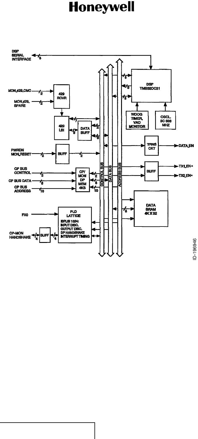
Processor CCA. See Figure 2003 (GRAPHIC 34-42-37-99B-813-A01) for the
schematic diagram of the monitor processor CCA. See Figure 7 (GRAPHIC
34-42-37-99B-808-A01) for the overall block diagram of the monitor processor
CCA.
(b) The Monitor Processor CCA supplies a second signal processor path. It uses a
DSP. The DSP processes the received signal and calibration signal, supplied in
digital form, from the main processor A/D converter. Also present are a clock, an
ARINC 429 receiver/selector, and static memory.
(c) The Monitor Processor CCA monitors how the main processor module processes
the signals. There are three interfaces between the main processor module and
the Monitor Processor CCA:
• Shared memory interface
• 429 interface
• DSP serial interface.
EFFECTIVITY
ALL 34-42-37 Page 36
10 Oct 2007
© Honeywell International Inc. Do not copy without express permission of Honeywell.
COMPONENT MAINTENANCE MANUAL
Part No. 066-50007
Figure 7. (Sheet 1 of 1) Monitor Processor Block Diagram (GRAPHIC 34-42-37-99B-808-A01)
EFFECTIVITY
ALL 34-42-37 Page 37
10 Oct 2007
© Honeywell International Inc. Do not copy without express permission of Honeywell.

COMPONENT MAINTENANCE MANUAL
Part No. 066-50007
(2) Shared Memory Interface
(a) The shared memory on the Monitor Processor CCA is the interface to the main
processor module. Two hardware semaphores located in the programmable logic
device U1 supply control of the interface. There is no nonvolatile memory on the
monitor processor module.
(b) The Monitor Processor CCA gets the program through the shared memory
interface, which is dual port RAM U1. After power-up the signal MON_RESET
(U11-48) is held active. The main processor module loads the monitor program in
the shared memory. Then the main processor takes the monitor out of reset,
which causes MON_RESET to go high. The DSP automatically loads its program
to the static RAMs U5, U6, U8, and U9.
(c) Programmable logic device U11 is a logic device, which is programmed
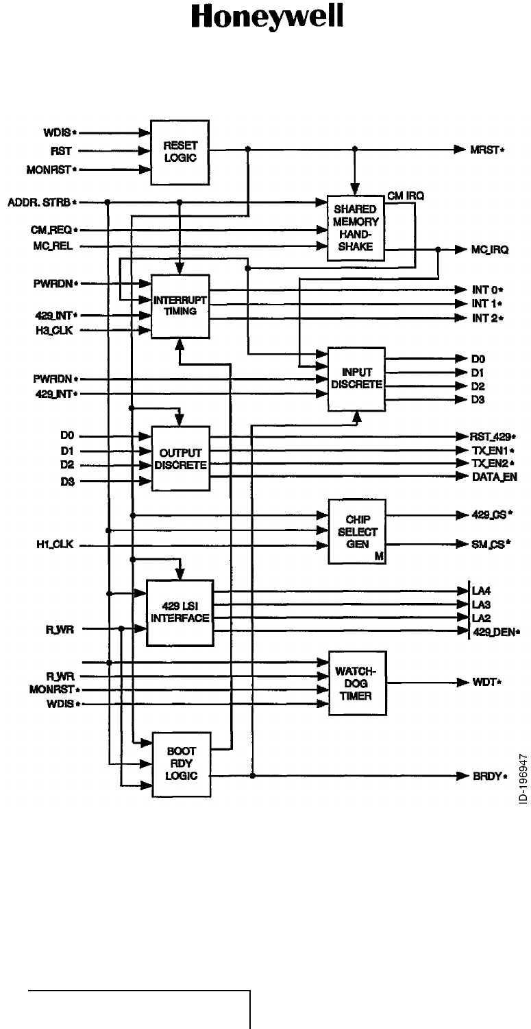
on the module by connector J6043 connector. Figure 8 (GRAPHIC
34-42-37-99B-809-A01) is a block diagram of U11.
(d) Inside the programmable logic device U11 device are:
• Reset logic function
• Interrupt timing
• Input discrete
• Output discrete
• Chip select generation for the ARINC 429 and dual port RAM
• ARINC 429 interfaces
• Data enable and address lines LA2, LA3 and LA4
• Watchdog timer logic
• Boot ready logic
• Shared memory logic.
(e) The communications for the shared memory is done with two flip-flops
implemented in the programmable logic device as shown in Figure 8 (GRAPHIC
34-42-37-99B-809-A01). The signal definitions are as follows:
1CM_REQ — CP to MON Request
• Input pulse from CP
• Latched to generate CM_IRQ.
2CM_IRQ — CP to MON Interrupt
• Active high interrupt to MON, generated from CM_REQ signal from CP
• Routed to CP/MON connector to be read by CP before next message is
sent
• Can also be read by MON as Input Discrete Bit DO
• Cleared by CM_REL.
3CM_REL — Clear CP to MON Interrupt
EFFECTIVITY
ALL 34-42-37 Page 38
10 Oct 2007
© Honeywell International Inc. Do not copy without express permission of Honeywell.

COMPONENT MAINTENANCE MANUAL
Part No. 066-50007
• Any write to Address 60 0000C or reset clears the CP to MON interrupt.
4MC_REQ — MON to CP Request
• Any write to Address 60 0010 sets MON to CP Interrupt.
5MC_IRQ — MON to CP Interrupt
• Active high interrupt to CP, sent through CP/MON connector
• Read by MON before next message is sent as D1 of Input Discretes
• Generated by MC_REQ, cleared by MC_REL.
6MC_REL — Clear MON to CP Interrupt
• Input pulse from CP/MON connector clears MON to CP Interrupt
• Reset also clears the interrupt.
(f) Each flip-flop has a request, clear, and a latched output. The latch of the
communication from main processor to monitor processor has a CM prefix on the
signal (control to monitor). In the other direction, the flip-flop has a MC prefix on
the signal (monitor to main). CM_IRQ and MC_IRQ are the latched outputs.
(g) When the main processor requests attention from the monitor processor CCA, it
sends a request signal CM_REQ to the input U11-3. The signal is then latched
and becomes CM_IRQ and remains latched until the monitor processor module
services the interrupt, and issues a clear signal. Once the latch is cleared,
CM_IRQ goes disabled.
EFFECTIVITY
ALL 34-42-37 Page 39
10 Oct 2007
© Honeywell International Inc. Do not copy without express permission of Honeywell.
COMPONENT MAINTENANCE MANUAL
Part No. 066-50007
Figure 8. (Sheet 1 of 1) U11 Functional Block Diagram (GRAPHIC 34-42-37-99B-809-A01)
EFFECTIVITY
ALL 34-42-37 Page 40
10 Oct 2007
© Honeywell International Inc. Do not copy without express permission of Honeywell.

COMPONENT MAINTENANCE MANUAL
Part No. 066-50007
(3) 429 Interface
(a) The Monitor Processor CCA listens to the 429 transmitters on the main processor
module. There are two modes, interrupt and continuous.
1In the interrupt mode if there is something wrong with either module, the
monitor processor module automatically shuts off the 429 transmitters on
the main processor module.
2In the continuous mode, the monitor processor module will not shut off
the transmitters.
(b) The signals that are used to shut off the transmitters are:
• XMON_BUS_DIS_#1 (J6018-74)
• XMON_BUS_DIS_#2 (J6018-75)
• XMON_DATA_ENABLE (J6018-76).
(c) In a default, as long as there is power to the monitor processor module the
transmitters are turned off.
(d) Device U10 is the ARINC 429 LSI and U12 is the ARINC 429 receiver. Receiver
U12 receives the transmitter signals from the main processor module. LSI U10
processes the signals. The programmable logic device does the ARINC 429
interrupt timing U11.
(e) The transistor Q1 supplies the drive to the monitor data enable discrete and to a
default position, which turns the transmitters on the main processor module off.
(4) DSP Serial Interface
(a) The DSP serial interface is connector J6045, which is two DSPs that
communicate with each other directly. One is on the Monitor Processor CCA,
which is U3. The other DSP is on the main processor CCA.
(b) The monitor processor module DSP U3 is be reset by:
• External reset from the main processor module
• 5 volt supply dipping below threshold value
• Watchdog timer reset.
(c) After monitor DSP U3 is reset by either the 5-volt monitor or the watchdog timer,
it stays reset until main processor issues a reset. When WDIS test point is
strapped to ground, both the 5-volt monitor and the watchdog timer are disabled.
In addition, BOOT RDY is written to in order to enable the watchdog function.
Until then, watchdog cannot cause reset.
(d) Device U4 is the supervisor and reset circuit, which has:
• Watchdog timer functions
• Reset function
• Over-voltage monitor function.
(e) The output reset signal goes to the programmable logic device U11.
EFFECTIVITY
ALL 34-42-37 Page 41
10 Oct 2007
© Honeywell International Inc. Do not copy without express permission of Honeywell.

COMPONENT MAINTENANCE MANUAL
Part No. 066-50007
(f) Device U7 is an address decoder, which generates memory chip select. Device
U13A generates the ready signal for the DSP U3. Connector J6045 is an
emulator connection used for development.
E. Power Supply Assembly (Subtask 34-42-37-870-013-A01)
(1) General
(a) The power supply assembly is a self-contained, high-efficiency, switching power
supply that converts the +28 V dc aircraft power into the needed dc operational
voltages. Three voltages are supplied:
•+5Vdc
•+12Vdc
•-12Vdc.
(b) The power supply assembly contains two modules:
• Power supply input module
• Power supply output module.
(c) See Figure 2008 (GRAPHIC 34-42-37-99B-818-A01) for a schematic
diagram of the power supply input module. See Figure 2009 (GRAPHIC
34-42-37-99B-819-A01) for a schematic diagram of the power supply output
module.
(2) Power Supply Input Module
(a) See Figure 2008 (GRAPHIC 34-42-37-99B-818-A01) for a schematic diagram of
the power supply input module. The aircraft + 28 V dc power is applied to the
input module through connector J3108, pins 1 thru 4. The aircraft + 28 V dc
voltage is applied to hot swap controller U1. Hot swap controller U1 is an 8-pin
hot swap controller that allows a board to be safely inserted and removed from a
live unit. The hot swap controller uses N-channel pass transistor Q1 so that the
board supply voltage can be ramped up at a programmable rate.
(b) The voltage on hot swap controller U1-1 is used to supply under-voltage lockout.
When the voltage ON pin, U1-1, is pulled below 1.233V an under-voltage
condition is detected. The GATE on U1-6 is pulled low to turn the transistor Q1
off. When the ON pin, U1-1, rises above 1.313V low-to-high threshold voltage,
the transistor Q1 is turned on again.
(c) The voltage on hot swap controller U1-2 (FB) is the power good comparator input.
It monitors the output voltage with an external resistive divider R3 and R4. When
the voltage on the FB pin is lower than the high-to-low threshold of 1.233V, the
PWRGD pin U1-3 is pulled low. This pin is not used on this module.
(d) The voltage on hot swap controller pin U1-5 is the timing input. External timing
capacitors, C3, C6, and C13 at this pin programs the maximum time U1 is allowed
to remain in current limit. When the part goes into current limit, a 77-microamp
pull-up current source starts to charge the timing capacitors. When the voltage
on the TIMER pin reaches 1.233V, the GATE pin (U1-6) is pulled low. The
pull-up current is turned off and a 3 microamp pull-down current discharges the
capacitors. When the TIMER pin falls below 0.5 Volts, the GATE pin either turns
EFFECTIVITY
ALL 34-42-37 Page 42
10 Oct 2007
© Honeywell International Inc. Do not copy without express permission of Honeywell.

COMPONENT MAINTENANCE MANUAL
Part No. 066-50007
on automatically or turns on once the ON pin is pulsed low to reset the internal
fault latch. If the ON pin is not cycled low, the GATE pin remains latched off.
(e) The voltage on hot swap controller pin U1-6 is the high side gate drive for the
N-channel transistor Q1. An internal charge pump guarantees at least 10 volts of
gate drive for supply voltages above 20 volts and 4.5 volts gate drive for supply
voltages between 10.8 and 20 volts. The rising slope of the voltage at the GATE
U1-6 is set by an external capacitor C5 connected from the GATE pin to GND and
an internal 10A pull-up current source from the charge pump output.
(f) When the current limit is reached, the GATE pin voltage adjusts to maintain a
constant voltage across the sense resistor while the timer capacitor starts to
charge. If the TIMER pin voltage exceeds 1.233V, the GATE pin is pulled low.
The GATE pin is pulled to GND when the ON pin is pulled low, the VCC supply
voltage drops below the 8.3V under-voltage lockout threshold or the TIMER pin
rises above 1.233V.
(g) The voltage on hot swap controller pin U1-7 is the current limit sense. A sense
resistor R8 is placed in the supply path between VCC and SENSE. The current
limit circuit regulates the voltage across the sense resistor to 47 millivolts if the
voltage on U1-2 is 0.5V or higher. If the voltage on U1-2 drops below 0.5V, the
voltage across the sense resistor decreases linearly and stops at 12 millivolts
when U1-2 is 0V. To defeat current limit, short the SENSE pin to the VCC pin.
(h) The 28 V dc output of the power supply input module is applied to the power
supply output module through connector J3302.
(3) Power Supply Output Module
(a) See Figure 2009 (GRAPHIC 34-42-37-99B-819-A01) for a schematic diagram of
the power supply output module. The power supply output module converts the
28 V dc from the hot swap controller into the three power supply voltages, +5 V
dc, +12 V dc, and -12 V dc.
(b) Each of the power supplies in the power supply output module use a PWM
controller and two switching transistors to develop each voltage. Table 7 lists the
PWMs and the transistors.
Table 7. Power Supply Components
Power Supply PWM Transistors
+5 V dc U2 Q3 and Q4
+12 V dc U1 Q1 and Q2
-12 V dc U3 Q5 and Q6
(c) All three of the supplies operate the same and only the +5 V dc supply is
described in this section.
(d) The 28 V dc from the hot swap controller is applied to PWM U2-15. The PWM
U2 is a high-voltage, wide input (10 to 55 Volts) synchronous, step-down
converter.Table 8 lists the pins of the PWM and the function of each pin.
EFFECTIVITY
ALL 34-42-37 Page 43
10 Oct 2007
© Honeywell International Inc. Do not copy without express permission of Honeywell.

COMPONENT MAINTENANCE MANUAL
Part No. 066-50007
Table 8. PWM Pin Functions
PWM Pin Function
U2-15 (VIN) +28 V dc input voltage
U2-2 (RT) Sets the internal oscillator ramp charge current and
switching frequency with resistor R23 and capacitor
C36.
U2-1 (KFF) Sets the output voltage and the slope of the voltage
ramp with resistor R25.
U2-6 (SD/SS) Soft start programming pin
U2-4 (SYNC) Synchronization input
U2-7 (VFB) Inverted input to the error amplifier
U2-12 (SW) Used for over-current sense
U2-16 (ILIM) Current limit pin, used to set the over-current
threshold.
U2-8 (COMP) Output of the error amplifier, input to the PWM
comparator.
U2-10 (LDRV) Gate drive for the N-channel synchronous rectifier
Q4. This pin switches from MOSFET Q4 on to
ground, MOSFET Q4 off
U2-14 (HDRV) Floating drive for the high-side P-channel MOSFET
Q5. This pin switches from MOSFET Q3 off to
MOSFET Q3 on
(e) The 28 V dc is converted to an ac voltage by the switching action off transistors
Q3 and Q4. Transistor Q3 is a P-channel MOSFET device. It is turned on and off
by the voltage on U2-14 (HDRV). Transistor Q4 is an N-channel MOSFET device.
It is turned on and off by the voltage on U2-10 (LDRV).
(f) The ac voltage generated by transistors Q3 and Q4 is rectified by diodes D14 and
D15. The rectified dc voltage is filtered by L2 and capacitors C30 thru C35.
F. Rear Interconnect Module (Subtask 34-42-37-870-014-A01)
(1) See Figure 2006 (GRAPHIC 34-42-37-99B-816-A01) for a schematic diagram of
the rear interconnect module. The rear interconnect module supplies the antenna
connections, power, and signal/data paths between the rear connector of the unit and
the ALA-52B internal circuits.
(2) The power supply input lines are straight through connections between rear connector
J1-BP-9 to pins 1 thru 4 of connector J14.
(3) The I/O signal lines are grouped on the schematic diagram into four categories:
• ARINC 429 inputs
• ARINC 429 outputs
EFFECTIVITY
ALL 34-42-37 Page 44
10 Oct 2007
© Honeywell International Inc. Do not copy without express permission of Honeywell.

COMPONENT MAINTENANCE MANUAL
Part No. 066-50007
• Discrete inputs
• Discrete outputs.
(4) Wirewound resistors, 100 ohm, 1 watt, along with TVS devices provide lightning
proctection for all ARINC inputs.
(5) All ARINC outputs have TVS devices to provide lightning protection. The lightning
current limiting is provided by the connected LRUs.
G. Front Panel Module (Subtask 34-42-37-870-015-A01)
(1) See Figure 2005 (GRAPHIC 34-42-37-99B-815-A01) for a schematic diagram of the
LED CCA. The LED CCA is an interface to an operator by the use of three LEDs
and a test switch.
(2) The LEDs D1, D2, and D3 display either red or green light when turned on. The
LED D1 shows the radio altimeter status. The LED D2 shows the receive antenna
status and D3 shows the transmit antenna status. The test switch S1 is used to
test the entire unit operation.
(3) A front panel connector is used for a handheld remote device or to program the unit.
EFFECTIVITY
ALL 34-42-37 Page 45
10 Oct 2007
© Honeywell International Inc. Do not copy without express permission of Honeywell.

COMPONENT MAINTENANCE MANUAL
Part No. 066-50007
Blank Page
EFFECTIVITY
ALL 34-42-37 Page 46
10 Oct 2007
© Honeywell International Inc. Do not copy without express permission of Honeywell.

COMPONENT MAINTENANCE MANUAL
Part No. 066-50007
TESTING AND FAULT ISOLATION
1. Planning Data (TASK 34-42-37-99C-801-A01)
A. Reason for the Job (Subtask 34-42-37-99C-001-A01)
(1) Use the test procedures in this section to do tests and fault isolate the ALA-52B.
(2) The function of the test procedures is to find if there is a failure in the operation
of the ALA-52B.
B. Job Setup Data (Subtask 34-42-37-99C-002-A01)
(1) You can use equivalent alternatives for the special tools, fixtures, equipment, and
consumable materials. The user must find equivalent alternatives.
(2) Refer to Table 1001 for the specified special tools, fixtures, and equipment in this
section. If this section refers to online data, refer to that data for the specified special
tools, fixtures, and equipment.
Table 1001. Special Tools, Fixtures, and Equipment
Number Name
11730A RF power sensor cable (CAGE 1MY97)
300-90273-0504 memory card interface module (CAGE 97896)
704-2899-001 ALA-52B ATP cable (CAGE 97896)
8074177-0001 ISP programming cable (CAGE 97896)
951-0409-00X COMNAV RTS (CAGE 97896)
951-0423-001 front panel interface adapter (CAGE 97896)
998-3804-5XX ATP software (CAGE 97896)
998-3853-503 (or later) Delta software (CAGE 97896)
Microsoft Windows 2000 or above (optional source)
ALT 52A Altitude simulator (CAGE 97896)
CA1267-60 RA power meter cable (CAGE 1UKX3)
CA1267-60 RA spectrum analyzer cable (CAGE 1UKX3)
E4418B RF power meter (CAGE 1MY97)
E9304A RF power sensor (CAGE 1MY97)
FSEB30 or FSIQ7 Spectrum analyzer (CAGE 82199)
Version 16.x LSC isp VM system software (CAGE 66675)
EFFECTIVITY
ALL 34-42-37 Page 1001
10 Oct 2007
© Honeywell International Inc. Do not copy without express permission of Honeywell.

COMPONENT MAINTENANCE MANUAL
Part No. 066-50007
WARNING: BEFORE YOU USE A MATERIAL, REFER TO THE MANUFACTURERS’
MATERIAL SAFETY DATA SHEETS. SOME MATERIALS CAN BE
DANGEROUS.
CAUTION: DO NOT USE MATERIALS THAT ARE NOT EQUIVALENT TO HONEYWELL
SPECIFIED MATERIALS. MATERIALS THAT ARE NOT EQUIVALENT
CAN CAUSE DAMAGE TO THE EQUIPMENT AND CAN MAKE THE
WARRANTY NOT APPLICABLE.
(3) Refer to Table 1002 for the specified consumable materials in this section. If this
section refers to online data, refer to that data for the specified consumable materials.
Table 1002. Consumable Materials
Number Name
Not applicable Not applicable
2. Procedure (TASK 34-42-37-810-801-A01)
A. Job Setup (Subtask 34-42-37-810-001-A01)
WARNING: BEFORE YOU USE A MATERIAL, REFER TO THE MANUFACTURERS’
MATERIAL SAFETY DATA SHEETS. SOME MATERIALS CAN BE DANGEROUS.
CAUTION: DO NOT USE MATERIALS THAT ARE NOT EQUIVALENT TO HONEYWELL
SPECIFIED MATERIALS. MATERIALS THAT ARE NOT EQUIVALENT CAN
CAUSE DAMAGE TO THE EQUIPMENT AND CAN MAKE THE WARRANTY
NOT APPLICABLE.
CAUTION: THE ALA-52B CONTAINS ESDS ITEMS. USE INDUSTRY APPROVED
PRECAUTIONS.
(1) Obey the precautions.
(2) Refer to Table 1003 for a list of test procedures that are included in this section.
Table 1003. Test Procedures
Procedure Part
Number Revision Used On Part Number Reference
076-1132-001 B066-50007-1111 Figure1001(GRAPHIC
34-42-37-99B-810-A01)
B. Testing of the ALA-52B (Subtask 34-42-37-810-002-A01)
(1) Use Figure 1001 (GRAPHIC 34-42-37-99B-810-A01) to do a test of the ALA-52B, Part
No. 066-50007-1111.
C. Job Close-up (Subtask 34-42-37-810-003-A01)
(1) Not applicable.
EFFECTIVITY
ALL 34-42-37 Page 1002
10 Oct 2007
© Honeywell International Inc. Do not copy without express permission of Honeywell.
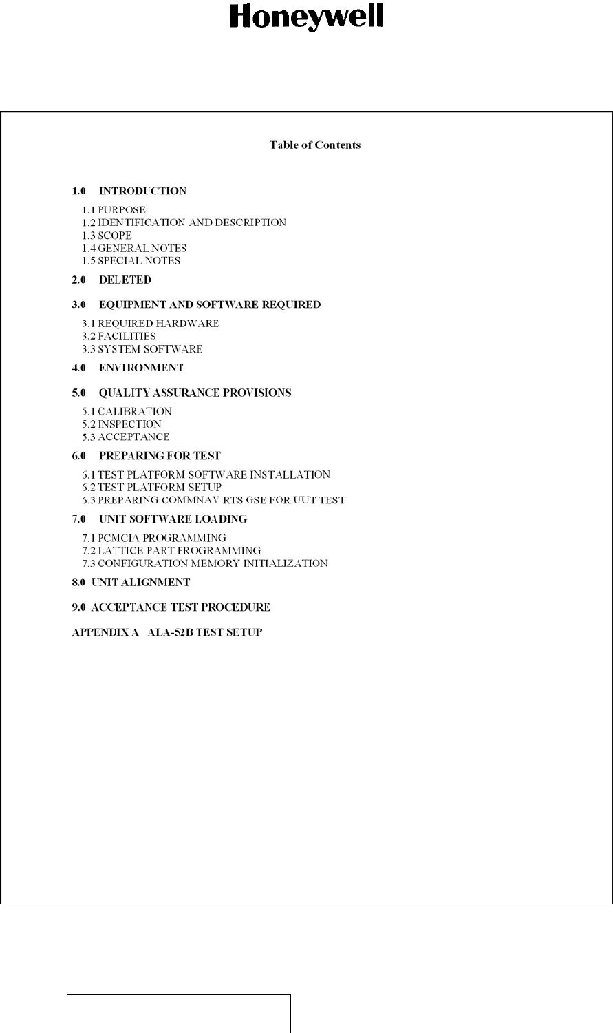
COMPONENT MAINTENANCE MANUAL
Part No. 066-50007
Figure 1001. (Sheet 1 of 12) ALA-52B Test Procedure (GRAPHIC 34-42-37-99B-810-A01)
EFFECTIVITY
ALL 34-42-37 Page 1003
10 Oct 2007
© Honeywell International Inc. Do not copy without express permission of Honeywell.
COMPONENT MAINTENANCE MANUAL
Part No. 066-50007
Figure 1001. (Sheet 2 of 12) ALA-52B Test Procedure (GRAPHIC 34-42-37-99B-810-A01)
EFFECTIVITY
ALL 34-42-37 Page 1004
10 Oct 2007
© Honeywell International Inc. Do not copy without express permission of Honeywell.
COMPONENT MAINTENANCE MANUAL
Part No. 066-50007
Figure 1001. (Sheet 3 of 12) ALA-52B Test Procedure (GRAPHIC 34-42-37-99B-810-A01)
EFFECTIVITY
ALL 34-42-37 Page 1005
10 Oct 2007
© Honeywell International Inc. Do not copy without express permission of Honeywell.
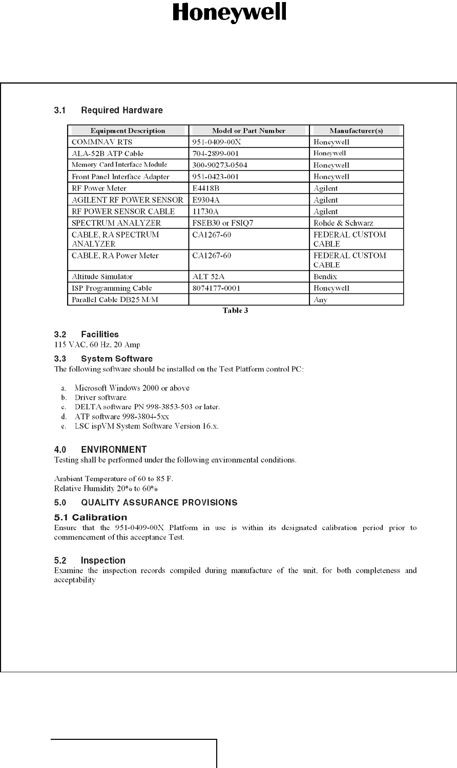
COMPONENT MAINTENANCE MANUAL
Part No. 066-50007
Figure 1001. (Sheet 4 of 12) ALA-52B Test Procedure (GRAPHIC 34-42-37-99B-810-A01)
EFFECTIVITY
ALL 34-42-37 Page 1006
10 Oct 2007
© Honeywell International Inc. Do not copy without express permission of Honeywell.
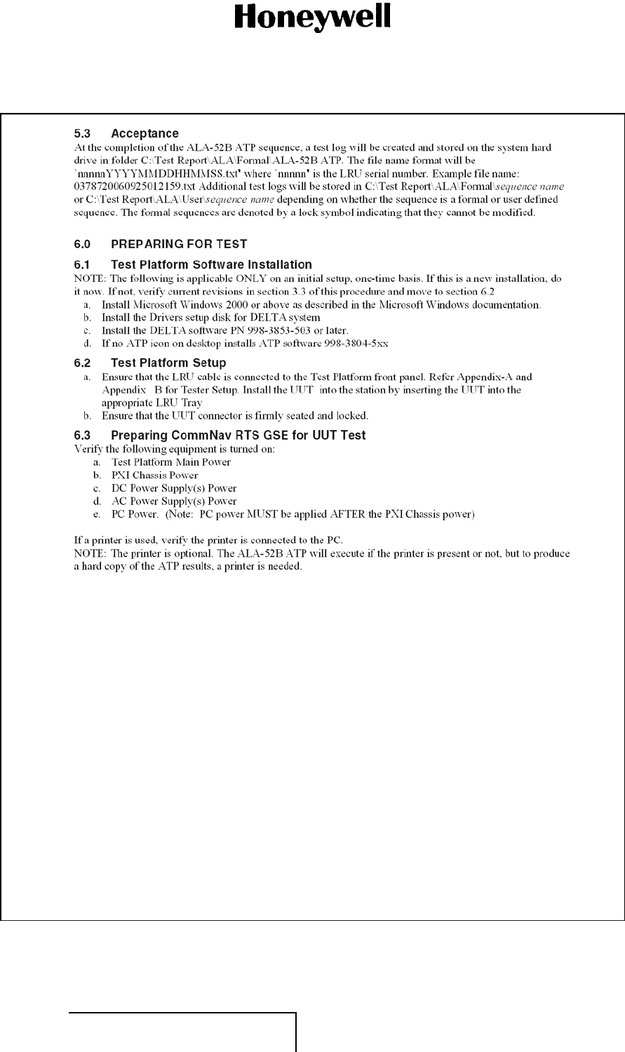
COMPONENT MAINTENANCE MANUAL
Part No. 066-50007
Figure 1001. (Sheet 5 of 12) ALA-52B Test Procedure (GRAPHIC 34-42-37-99B-810-A01)
EFFECTIVITY
ALL 34-42-37 Page 1007
10 Oct 2007
© Honeywell International Inc. Do not copy without express permission of Honeywell.
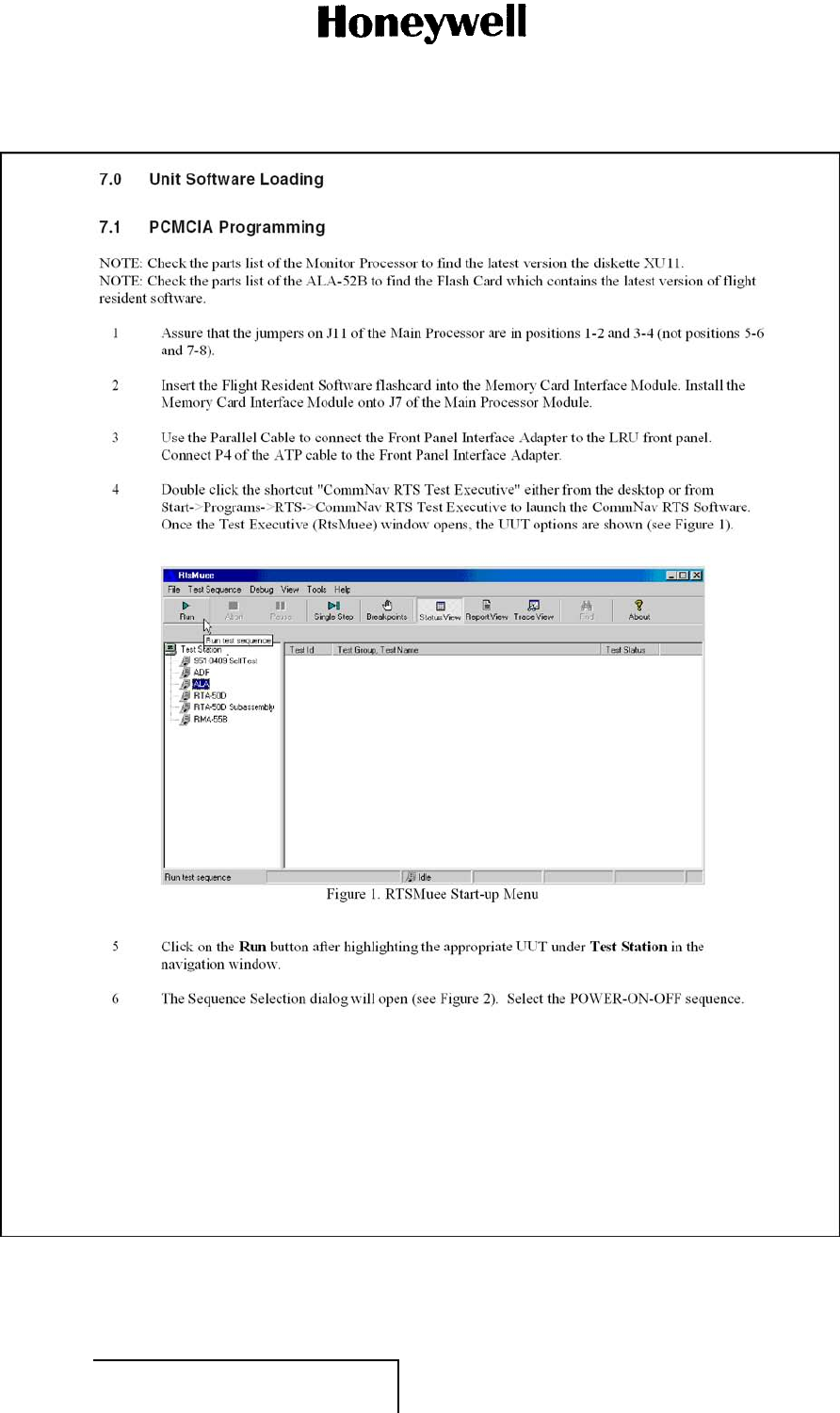
COMPONENT MAINTENANCE MANUAL
Part No. 066-50007
Figure 1001. (Sheet 6 of 12) ALA-52B Test Procedure (GRAPHIC 34-42-37-99B-810-A01)
EFFECTIVITY
ALL 34-42-37 Page 1008
10 Oct 2007
© Honeywell International Inc. Do not copy without express permission of Honeywell.
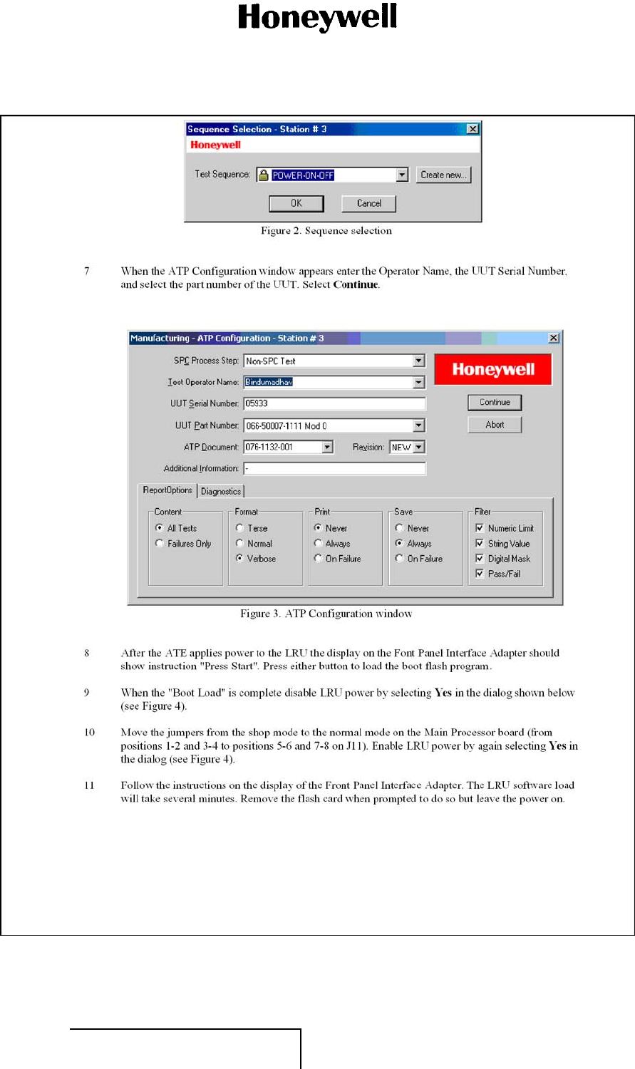
COMPONENT MAINTENANCE MANUAL
Part No. 066-50007
Figure 1001. (Sheet 7 of 12) ALA-52B Test Procedure (GRAPHIC 34-42-37-99B-810-A01)
EFFECTIVITY
ALL 34-42-37 Page 1009
10 Oct 2007
© Honeywell International Inc. Do not copy without express permission of Honeywell.
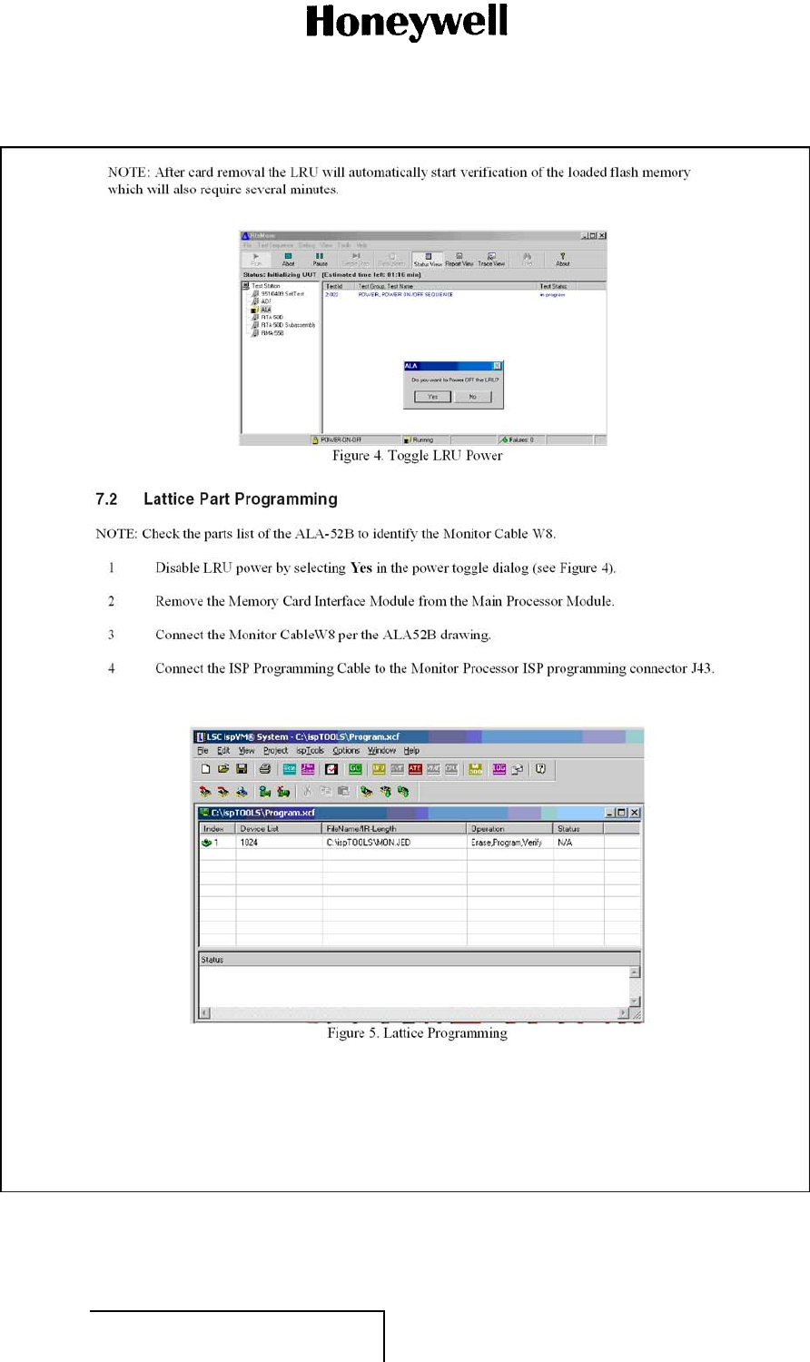
COMPONENT MAINTENANCE MANUAL
Part No. 066-50007
Figure 1001. (Sheet 8 of 12) ALA-52B Test Procedure (GRAPHIC 34-42-37-99B-810-A01)
EFFECTIVITY
ALL 34-42-37 Page 1010
10 Oct 2007
© Honeywell International Inc. Do not copy without express permission of Honeywell.
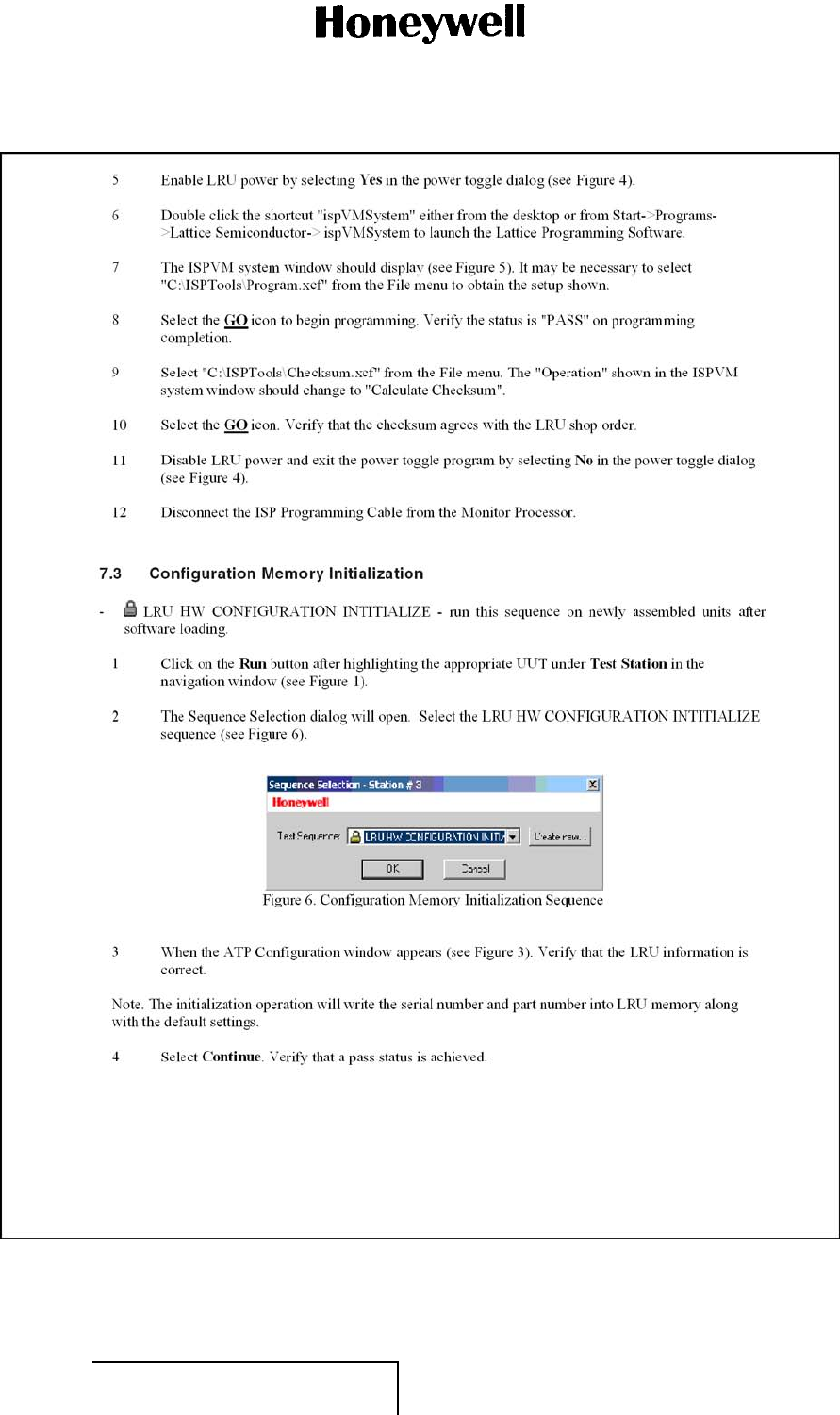
COMPONENT MAINTENANCE MANUAL
Part No. 066-50007
Figure 1001. (Sheet 9 of 12) ALA-52B Test Procedure (GRAPHIC 34-42-37-99B-810-A01)
EFFECTIVITY
ALL 34-42-37 Page 1011
10 Oct 2007
© Honeywell International Inc. Do not copy without express permission of Honeywell.
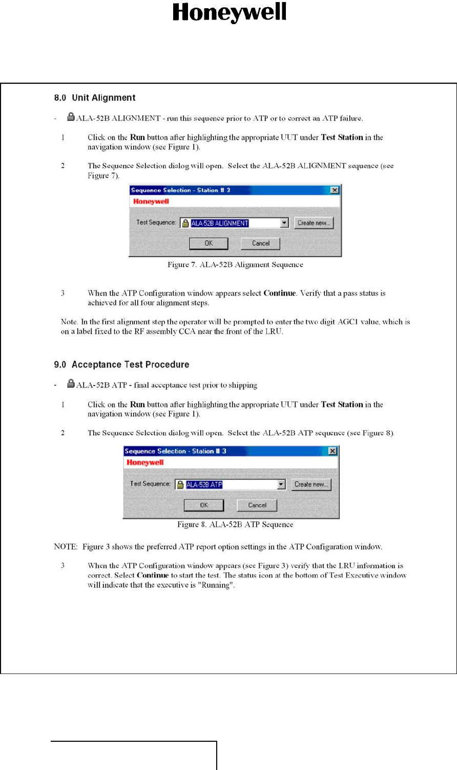
COMPONENT MAINTENANCE MANUAL
Part No. 066-50007
Figure 1001. (Sheet 10 of 12) ALA-52B Test Procedure (GRAPHIC 34-42-37-99B-810-A01)
EFFECTIVITY
ALL 34-42-37 Page 1012
10 Oct 2007
© Honeywell International Inc. Do not copy without express permission of Honeywell.

COMPONENT MAINTENANCE MANUAL
Part No. 066-50007
Figure 1001. (Sheet 11 of 12) ALA-52B Test Procedure (GRAPHIC 34-42-37-99B-810-A01)
EFFECTIVITY
ALL 34-42-37 Page 1013
10 Oct 2007
© Honeywell International Inc. Do not copy without express permission of Honeywell.
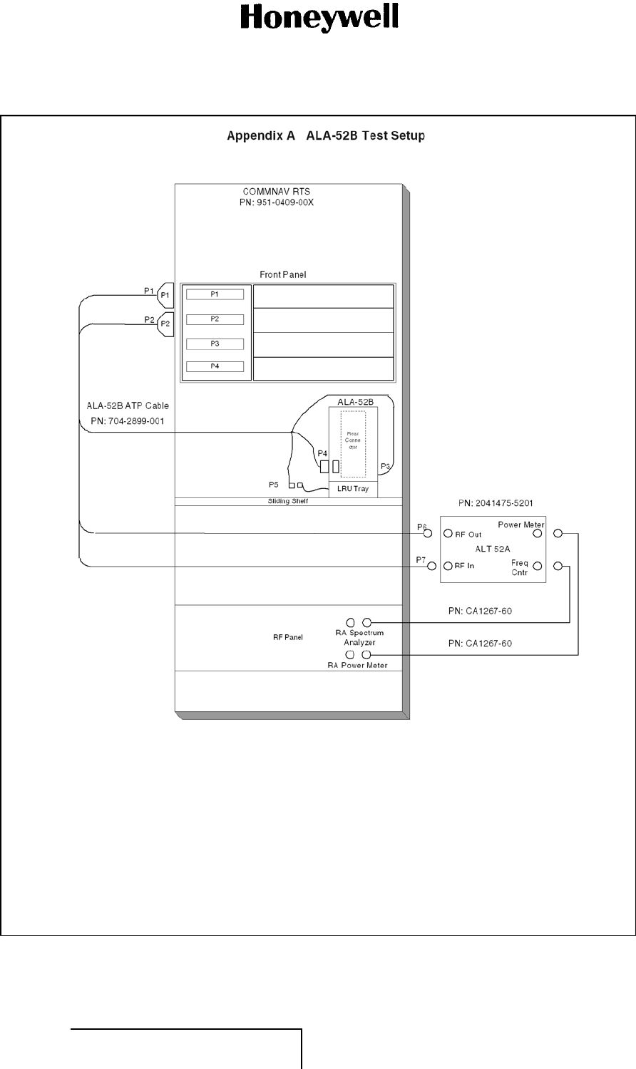
COMPONENT MAINTENANCE MANUAL
Part No. 066-50007
Figure 1001. (Sheet 12 of 12) ALA-52B Test Procedure (GRAPHIC 34-42-37-99B-810-A01)
EFFECTIVITY
ALL 34-42-37 Page 1014
10 Oct 2007
© Honeywell International Inc. Do not copy without express permission of Honeywell.