Hp Car Stereo System 3490A Users Manual
3490A to the manual 099e4e8a-d632-4bb5-aded-017e2f4dd5c2
2015-02-09
: Hp Hp-Car-Stereo-System-3490A-Users-Manual-545441 hp-car-stereo-system-3490a-users-manual-545441 hp pdf
Open the PDF directly: View PDF ![]() .
.
Page Count: 298 [warning: Documents this large are best viewed by clicking the View PDF Link!]
o
.(D
s
c
Lg-F
A l-
T
R
E
P
oAruGAFiä3 s€Rtvt#ffi MAru
PACKARD
7:'
;s,
;;:''
tt,,,,t,
?i'-"
';i: '
;
T
!-,
ö.,
A
(o.
D=.'
M
U
ITIM
ETE
R
349:04
HEWLETT
HEWLE"WPACKARD
CE
RTI
FI
CATI
O
tII
The Hewlett-Paclnrd
Company
certifins that this instrammt was
thoroughly
tested,
ond. inspected
and fourd to meet its pu,blished
specifications
whm it was
shipped
lrom the
factorU.
The Hewlett-
Paclard Com,pany
further certifies tlmt its calibration rneo$re-
m,mts
are traceable
to the U.S.
Natiornl Bureau
of Standards
to
tlrc ertmt allowed
by the Brneau's
calibration
facility.
WARRA]TTY
ATD
ASSISTAITCE
All Hewlett-Packard
products
are warranted against defects in
materials
and workrnanship."'This
warranty applies
for one
year
from the date of delivery,
or, in'the case of certain
major compo-
nents
listed in the operating
manual,
for the specified
period.
We
will repair or replace
products
which
prove
to be defective
during
the warranty
period
provided
they
are returned
to Hewlett-
Packard.
No other warranty is expressed
or implied. We are not
liable
for consequential
damages.
Service
contracts
or customer
assistance
agreements
are available
for Hewlett-Packard
products
that require maintenance
and re-
pair on-site.
For any
assistance,
contact
your
nearest
Hewlett-Packard
Sales
and
Service
Office. Addresses
are
provided
at the back
of this manual.
v
OPERATING
AITD
SERYICE
MAIIUAI
Manual Part No.
03490-90014
Microfiche Part No. 03490-90064
MODEL
3490A
M U tTIM ETE R
!;:,'
;.t; .:
:i;
:
-:
!:.. '.
::::
"
The main
body of this
manual
applies to
Serial Prefix 1211A
Any changes
made in instruments
manufactured
after this
printing will be found in a "Manual Changes"
supplement
supplied with this manual. Be sure
.
to examine this
supplement,
if one exists
for this manual,
for any changes
which apply to your instrument
and record
these
changes
in
the manual.
Backdatinginformation
for instruments
manu-
factured
before
this printing will be found in Section VIII.
Copyright Hewlett-Pack
afi Company | 97 2
P.O.
Box
301,
l,oveland,
Colorado 80537 U.S.A
Printed:
APRIL
1974
Model3490A
TABLE OF
Section Page
I. GENERALINFORMATION... ......I-1
l-1. Introduction ...1-l
l-5. Specifications
.... .'-.l-l
l-8. Options -......1-1
l-10. AccessoriesSupplied ...1-l
l-12. AccessoriesAvailable ...1-1
l-14. Instrument
and Manual
Identification ......1-2
Section Page
II. INSTALLATION
ANDINTERFACE
. .
.. ... .2-I
2-l- Introduction ..-2-l
2-3. Initiallnspection.. ....2-l
2-5. Power Requirements - . .2-l
2-8. PowerCordsandReceptacles
.. -
.....2-l
2-10. GroundingRequirements...
. . .
.. .
-
..2-1
2-14. Environmental
Requirements
. . . . - . . . 2-l
2-16. Installation ....2-2
2-17. BenchUse -...2-2
2-19. RackMounting.... ....
-...2-2
2-21. Installationofoptions .... -...2-2
2-23. Isolated
Data OutPut
Option 021
(-hp
lll2lA) .. . . . .. .2-2
2-25. Isolated Remote
OPtionO22
(hpllr22{). ---..2-2
2-27. Option050andOption060
..
..... -2-3
2-29. InterfaceConnections ...'....2-3
2-30. Data Output
OPtion
021 .. . -2:2
2-32. RemoteControlOption
022..... -. -2-3
2-34. Rear Input . . .24
2-36. General
Purpose
Interface
Bus
Connections ...'-..24
2-38. InterfaceCableLength ......2-6
24O Trigger
Connections,
GPIBOption030 .......2-8
242. Sample/Hold
Connections, -'-''
Option
UO|O4| . .. . .. .
.2-8
246. RepackagingforShipment .....2-9
Section Page
Iil. OPERATING
INSTRUCTIONS.
. . .. ..3-I
3-1. Introduction ...3-1
3-3. InstrumentCapabilities --...'.3-l
3-4- Standardlnstrument ....'...3-1
3-6. Output and Remote
Control
Options .3-l
3-9. Sample/Hold
Option
040 or &15 . ' . .3-1
3-ll. Ratio Option
080
.
. .. .. . .
. .3-l
3-13. Front and Rear
Panel
Description . - . . -3-l
3-15. MadmumlnputVoltages
...........3-l
3-17. General Operatinglnstructions
. -... ..3-2
3-18. Turn-OnandWarm-Up ......3-2
3-20. Guarding .....3'2
3-24. FloatingMeasurements
..... ..... -.3-2
3-26. Overrange
Measurements
. . . . . . . . . - 3-3
3-28. Overloadlndication ........3-3
3-30. Rangelndication
.. ...-....3-3
3-32. Functionlndication ........3-3
Table
of Contents
CONTENTS
Section
III (cont'd) Page
3-34. Autoranging ........3-3
3-36. ManualTrigger ......3-3
3-38. Self-TestOperation ....3-3
340. DCVoltageMeasurements
........... 3-3
342. DC Sample
Rate
and
ResponseTime. ....34
344. Input Resistance
.. . .. .. ... .34
346. ACVoltageMeasurements .....34
348. AC Sample
Rate and
ResponseTime. ....34
3-50. FrequencyRange. ...34
3-52. Inputlmpedance
.. ........34
3-54. HarmonicDistortion ........34
3-56. Resistance
Measurements
. . . . . . . . . . . .34
3-58. InputConnections
. ........3-5
3-60. Ohms
Signal Voltage
and Current
. . . .
3-5
3-62- Ohmmeter
Sample
Rate and
ResponseTime. ....3-5
3-64. External Trigger
(Option
020) . . .. . . . . 3-5
3-66. Data Output (Option O2l) . . . . .3-5
3-68. Output Signals
and
l,evels . . . .
3-5
3-71. Input Sigrals
and hvels . . . . .34
3-73. Data Output
Isolation . .. . . . .3-6
3-75. Remote Control
(Option
022) .. .. . . . .34
3-77. InputSignal Requirements
..... ....34
3-79. OutputSignals ......36
3-81. Remote
Programming
Procedure . . . .34
3-83. Remote Control
of Test
Function . . .34
3-85. Remote Control
Isolation . . . .34
3-81. General
Purpose
Interface Bus
I/O(Option030) . ........3-7
3-90. GPIB
Bus
Signals . . . .3-7
3-101. Talk Only (No Controller) . . . . . . . . .
3-8
3-103. GPIB Control
of3490A .. . . .3-8
3-131. GPIB Operating
Example . . . 3-13
': 3-136. Control
by Marked Card
Programmer .....-3-14
3-139. Sample/Hold
Measurements
(Option
040
or 045)
.. . . . .3-15
3-140. Definition of Sample/Hold
Terms . . . 3-15
3-152. Special S/H
Operating
Considerations
.... ......3-16
3-156. Guard Connection
in Sample/Hold
Measurements
..... ......3-16
3-158. Input
Signal
Limitations . .. .3-16
3-160. Sample/Hold
Trigger Signal
Requirements
..... .....'3-16
3-165. Initiating
a
Sample/Hold
Measurement .... -3-17
3-173. Usingthe
Track/HoldMode
.... .. . 3-18
3-179. Using
the Acquire/Hold
Mode . . . . .3-20
3-182. Using
50
Hz or 60
Hz
Power
Source
.
3-21
3-184.
Ratio
Measurements
(Option
080). .
. .3-21
3-186. External
Reference
Voltages
- - -. ...3-21
3-188. InputConnections
. .......3-21
3-190. RatioDisplaY ......3'21
3-192. RatioMeasurementProcedure
.' -
-
-3-21
iii
Table of Contents Model 34904
TABLE
0F C0NTENTS
(Gont'd)
Section Page
IV. THEORYOFOPERATION
. ........4-I
4-1. Introduction ...4-l
4-3. General Theory
of Operation . . .4-l
4-5. Signal Conditioning
Circuits . . . . . . . . 4-l
4-7. ReferenceVoltages ...4-l
4-9. DC
Amplifier ...... .4-l
4-ll. Analog-to-Dgital
Converter
. . . . .. . . 4-l
4-13. Logrc . ......4-l
4-15. Display ......4:2
4-17. Range
and Function
Control . . . -
. . . 4-2
4-19. DC
Analog
Circuits .. - .4-2
4:21. InputAttenuator
.. ........4-z
4-23. DC
Amplifier . ..... .+3
4-25. DC Amplifier
Gain . ... .....4-3
4-27. SwitchingCircuits ....4-3
4-29. BootstrapCircuit ....4-3
4-31. Reference
Voltages . . .4-3
4-33. OverloadProtection ........43
4-35. Leakage
Control .....43
4-37. DC
Amplifier
Auto Zero . . . . .4-3
4-39. Integrator
Circuits .
.. .
.4-s
440. Dual-Slope
Integration .. .,..4-s
42. IntegratingAmplifier .......4-5
4
44. x 20 Amplifiet
-.. . . .M
446. ZeroDelectAmplifier ......M
4-48. ElectronicSwitch ....M
4-50. Integrator
Auto Zero .
.
-
... .44
4-52. AC
Converter . . .44
4-54. AC
Attenuators
.. ...44
4-56. ConverterAmplifier ........44
4-58. Rectifier
and Filter . . .
+7
440. OhmsConverter.... ...*7
442. CunentSource ......4-7
444. Ohmmeter Power
Supply .
. . .4-7 ,"
4-66. OhmmeterReference .......+g
448. InputProtection... ..+9.
4:70. Dsplay
Assembly
(Figure
7-27).......44
4-71. Display
Units . ......4-g
4-73. ScanGenerator.... ........+g
4-75. ScanDecoder .......4-8
4-77. PolarityDisplay .....4-8
4-79. Decimals
and
Annunciators
. . . . . . . . 4-B
4-81.
IngicCircuits
.... ....4-8
442. Clock. ......43
444. DataCounter .......+9
4-86. Buffers ......+9
+88. Timing
Counter .
.. . .
+9
4-90. Algorithmic
State Machine
. . . . . . . . +ll
4-105. Input
Polarity
Storage .. .
.
. 4_12
4-107. Transfer
andZero
Detect . . . 4-12
4-113. OverloadStorage ...+13
+l15. DC
Switching
Logic . . . +13
+117.
ReferenceSupplies ...+13
4-1
18. Voltage
Measurements
.... ....... +13
+122. RatioMeasurements
(Option080)
. ....+14
+118.
Front
Panel
Switching .
... . . .4-15
ir-
Section IV (cont'd) page
4-130. PowerSupplies
... ...4-15
4-132.
Self-TestFunction ....4-16
4-134. LogicTest,No.
I . ..+16
+137. lOVRangeZero,TestNo.
2 . ..... +17
4-139. TurnoverError,
TestNo.
3 . ....... 4-17
+141. f ReferenceCheck,TestNo.
4 ..... 4-17
4-143. 0.1 VRangeZero,TestNo.
5
. ..... 4-17
4-145. x.0l Atten.,
x 100
Gain,
TestNo.6.... ..4-17
+147. Ohms
Reference,TestNo.
7 .
......4-17
4-149.
BCD
Remote
Expand
Option
020
(FigureT-31) .....4-t7
4-150. Outguard Power
Supply - . . .4-l,l
4-152. Isolated
Trigger
and Hold . . .
zt-18
4-154. Sample/HoldTriggerCircuits
.
.. .. . 4-18
4-158.
Data
Output
Option
021
.. . .
.4-18
+160. DataMultiplexers
.. .......4-18
4-162. DataOutputSequential
Logic ..... 4-18
4-164. Data
Clock . . +lg
+166. Isolation
Assembly . .4-18
4-168.
ShiftRegisters
.... .......4-19
+170. DataFlag ...+19
4-172.
PrinterHold. ......+19
4-174.
Remote
Control
Option 022 .
.. .
. .. .+19
4-176. Circuitlsolation -...+19
+178. RemoteEnable ...-.+19
4-180. OutguardMultiplexer ......+19
4-182. Remote
Sequential
Logrc . . - 4-19
4-184.
Program
Flag
. ... -.+19
+186. Data
Clock . .4-20
4-188. Shift
Registers .....4-20
. +19O. Local/RemoteMultiplexers
. ......4-20
4-192. Local/RemoteFlip-Flop ....+2O
4:194. Data Flag .
. .4-20
4-196.
General Purpose
Interface
Bus
I/O
(Option
030) . .. .. . . .4-20
+198. GPIBSystem ......4-20
4-201. Basic
Theory
of GPIB I/O
Circuits
. . +21
4-204. GPIB
System
Operation . . . .4-21
4-212.
Sample/Hold
Option 040 or
045 . . . . .4-22
+214. Track/Hold
Mode . . .4-22
+216. Acquire/HoldMode
. ......4-22
4-218. Sample/HoldMeasurement
Sequence ..+22
4-221. Sample/HoldAnalogCircuits
... ...4-23
4-228. Sample/Hold
Logic
Circuits . . . . . . .
+25
Section Pase
V. MAINTENANCE
... ... . s]r
5-1. Introduction .....5-l
5-3. RecommendedTestEquipment.
.. ... .. .
5-l
5-5. TestRecord .....5-l
5-7. PerformanceTests. ......5-l
5-9. DCVoltmeterAccuracyTest.. ...5-l
5-l l. AC Voltmeter
Accuracy
Tests
. . . .
5-l
5-15.
OhmmeterAccuracyTests.. .... -5-2
5-16. PreferredMethod ......5-2
Model3490A Table
of Contents
rABLE
OF
CONTENTS
(Cont,d)
Section
V (cont'd) Page Section page
5-18. Ätemate
Method . .
... .5-2 VII. TROUBLESHOOTING
AND
5-2O-D0Common-ModeRejectionTest ......5-2 CIRCUITDIAGRAMS .......7-l
5-22.
A9Common-ModeRejectionTest
......54 7-1. Introduction ...7-l
5-24-
AC Normal-Mode
Rejection
Test
.. ......54 7-3. Preliminary
Troubleshooting
... ... . . .7-l
5-26.
DcVoltmeterlnput 7'5. TroubleshootingTrees ........7-l
Resistance
Test
.. .... .54 7-7- Access
for
Servicing .. . .7-l
5-28.
AcVoltmeterlnput 7--9. PowerSupplyChecks ........7-l
ImpedanceTest. .....S-5 7-13.
DCAnalogCircuits ....7-2
5-30. Sampli/Hold
Performance 7-15- ,{2
Assembly
Exchange . . . . .7-2
(Option04OlO45) .....5-5 7-17- DCAmplifierChecks .......7-2
5-32. Sample/Hold DC Measurement 7-22. DC
Amplifier
Switching
Circuits
. . . . .7-3
AccuracyTest.. ......54 7-25. ReplacementofQCR3Ol ....7-3
5-34.
Sample/Hold Response
Test ... ..5-6 7-27. A-to-D
Conversion
Circuit
Checks
. .. . .7-3
5-36. RatioPerformance(Option080)..
......5-7 711. IntegratorTroubleshooting
..........74
5-38. DC/DC Ratio
Accuracy
Tests
541. AClDCRatioAccuracyTest .....5-g 737' OhmsConverterTroubleshootlng.....74
543- ExternalReferenceinput !19 DisplayTroubleshooting
............7-s
ResistanceTest.. .....5-8 t4z' LogicTroubleshooting
545. GPIB
Operational
Check
(Option
030) .. .5-8 - ,6 _ Suggestions
.. . . . .. .7-5
547. General
Test Procedure
. .-.
. .
. . 5-l I t4ö- Data
Output
Troubleshooting
549. Test Procedure
Using (Option
O2l) . . . . . .7-5
Model
98204
Calcrilator . . . . . 5-l
l 7-50. Remote
Control
Troubleshooting
5-51.
AdjustmentProcedures...
.....5-14 (OptionO22)
. .....7-5
5-53. PowerSupplyAdjustment ......5-14 t-)2' GPIBTroubleshooting
5-55.
DCZeroAdjustments.. .......5-15 (Option030)
. .....'l-5
5-57.
ReferenceAdjustments...
.....S-15 !-)5' GeneralChecks ......7-s
5-59.
DC
Amplifier
Adjustments
561.
ACCorrverterAdjustments .....5-15 !'t7' ExternalTriggeiCircuitCheck.
.....74
563. lVRangeAdjüstments ......s-15 1-t?'sample/HoldSJrvicing ........74
544. l0VRangeAdjustments .....5-16 !-bu' AccesstoSample/HoldCircuits
.....74
5-65. 100
V Range
Aäjustments . . . .
5-16 743' Operating
the
3490A
with
5-66.
OhmmeterAdjustments.. ......5-16 Sample/HoldAssembliesRemoved..T6
5-69.Sample/HoldAdjustments. .....5-16 !t2 Sample/HoldTroubleshootingTrees...T4
5-71. Offset
Gain
Adjustment . .. .. .5-16 t4'1. Ratio
Troubleshooting . . .. . . ..7-8
5-73. Offset
Adjustment
. . . .5-17 749- External
Reference
Amplifier
5-75. Dielectric
Absorption
Adjustment
. .. .5-17 Checks
. .
. .
.7A
5-77. Response
Adjustment
...... ..
S-iA
t^'
5-79.
Ratio
Reference
Adjustments . . .5-lg r. 7'73. Reference
Polarity
Logic
Checks
. . . . 7-8
7-75. SchematicNores. .....7_g
Section page 7'77. Logic
Gate
Symbols . . . .7-g
VI. REPLACEABLEPARTS ......6-I SCCtiON PAgE
6-1. Introduction ...6:l VlI. BACKDATING
.... ... .8_l
6-1 Orderinglnformation ........6_l g_1.
Introduction .....g_l
6-6. Non-Listedparts
. .....6-l g_3.
Change
Sequence ........ g_l
6-8. ProprietaryParts. .....6-l g-5. partsNotUsted. ........g_l
APPENDICES
A. Code
List
of Manufacturers
B. Sales
and
Service
Offices
Table of Contents Model 34904
LIST
OF
ILLUSTBATIONS
Figure Page
2-1 . Line Voltage Selection . . .2-l
2-2. PowerCordConfigurations .... .......2-l
2-3. Model3490ADimensions ......2-2
24. Installation of Isolated
BCD
Output
and
Remote
Options .
. .. . .. .2-3
2-5. Data OutputConnections, Option 021 ........24
2-6. Remote
Input
Connections, Option
022 ... . .
. . 2-5
2-7. RearlnputConnectorandCable .......2-6
2-8. Interface Bus Cables . . . .2-6
2-9. General
Purpose Interface Bus
Connections. . . . .2-J
2-10. Tigger Connections, GPIB Option 030 . . .. . . . .2-8
2-l I . Trigger Connections
S/H Option
045 . . . -
. . . . . . 2-8
3-1. Front and
Rear
Panel . . . . 3-0
3-2. Connecting the Guard . . .3-2
3-3. OhmmeterlnputConnections . ........3-5
34. External Trigger
Sequence
(Option
020) ... . .. . 3-5
3-5. Option
021
Printout . . . .3-6
3-6. Remote Program
Sequence
(Option 022) . . . . . .3-7
3-7 . Position of Jumper
Wires on Outguard
Mother
Board
Assemblv A31
3-8. Timing Diagram,
3490A
Addressed
to Listen . . 3-l I
3-9. Timing Diagram, 3490A
Addressed
to Talk . . . .3-12
3-10.
Example ofMarked CardProgramming
. . . . . .. 3-15
3-1 l. Typical Response to a
Step
InputVoltage.... ..3-18
3-12.
Di$tizingaRamp .....3-19
3-13. Using Delayed-Sweep
Oscilloscope
in
RampLinearityMeasurements
. . ...3-20
3-14. Filter
Output Measurement . . . .3-2O
3-l 5. Measurement
of a Step
Input . . . 3-21
3-16.
RatiolnputConnections. .....3-21
4-1
. Dual-SlopeIntegration ...4-1
Figure Page
4-23. Waveforms
Illustrating
Acquire/HoldMode. ......4-22
4-24. Simplified
Diagram
and
Operationof
S/HCircuit
A.. .. ....4-23
4-25. Simplified Diagram
of S/H
Circuit
B . . . . .. .. .4-24
4-26. Aebctric Absorption
Compensation . . . . . . - . . 4-25
4-27. Sample/Hole
Logic Block Diagram .. . .... . . . 4-25
4-28. Block
Diagram
of S/H Timing
andTriggerCircuits .......4-26
4-29. Sample/Hold
Trigger Timing . . .4-26
4-30.
Sample/HoldMeasurement
Sequence
.. .. -...+28
4-31. Sample/Hold
Simplified Diagram
and
Measurement
Sequence ....+29
5-1. AC Voltmeter
High Frequency
AccuracyTest.. .....5-2
5-2. DCCommon-Mode
RejectionTest .....5-3
5-3. AC Common-Mode
Rejection Test . . . . .54
54. ACNormal-Mode
RejectionTest .. ..... 5-5
5-5. DCVoltmeterlnput
Resistance Test .. . . . . .. .
. 5-5
5-6. ACVoltmeter Input Impedance Test
.
... . ..... 5-6
5-7. Sample/Hold Response Test . -
. .5-7
5-8. External
Reference
Input
ResistanceTest.. ....5-9
5-9. Location
of Adjustments,
Standard3490A ....5-14
5-10.
Location of
Sample/HoldAdjustments
.. .....5-17
5-ll. Location of Ratio Adjustments .......5-18
6-1. ChassisParts
. ..6-30
G2. BindingPost
Assembly
.... ...6-31
6-3. SwitchAssembly ......G31
7-1. Switching
Inputs to A2U2 . .
.. . .7-3
7-2. SwitchingOutputsofAlU4Ol ........1-3
3-8
4-2. BasicDiagramandOperation..... .....1"2 .:7-3. Sample/HoldAssembly ........7-7
4-3. SimplifiedDiagram,DCAmplifier ......4-3 14. deneralTroubleshootingTree ....7-ll17-12
44. Measurement
Sequence .. . ... -
.44 iL' l-5. DC Ana1os Troubleshootins
Tree .]-1317-14
4-5. Simplified Diagram,
Integrator Circuits . . . . - . . . 4-6 j 4. AC Conveiter
Troubleshooling Tree . . . . . i,-1511-16
4-6. Simplified Diagram,
AC Converter
. . . . . . . . . . . .4-7 7-7 . Ohms Converter Troubleshooting
Tree . . .7-17
17-18
4-1. SimplifiedDiagram,OhmsConverter..........4-8 7-9. DisplayTroubleshootingTree ....|.-1917-20
4-8. Block
Diagram,
Clock and
Counters . . . .4-9 j-9. Loeic Test Troubleshooting
Tree . .7-21
17-22
4-9. TypicalStateMachineBlockDiagram ...4-g 7-tO. I_ofibClockTroubleshooti"ngTree.......l-2317-24
4-10. Block Diagram,
Main Logic 7-l l. Data
Output Troubleshooting
Tree
ASMFlowChart. ...4-10 option}2l .. ..1-2517-26
4-l l. Block
Diagram,
Main
Logic
Circuits . . . .4-11 7-12. Remote Troubleshooting
Tree,
4-12. Block Diagram,
Qualifier
Multiplexer . .4-12 option 022 .
. . .i-2717-28
4-13. Simplified Diagram, Reference 7-13. GPIB
I/O Troubleshooting
Tree,
and Ratio
Circuits . . .4-13 Option 030 . . . .7-2917-30
4-14. Simplified Diagram, External 7-14.
Sample/Hold
General Troubleshooting
Reference
Circuits . . 4-14 Tree . .
.1-31
17-32
4-15. Input Bias
Compensation
. .
. . .
.4-15 7-1
5. Sample/Hold
Logic
Troubleshooting
4-16. ReferencePolarityLogic. .....4-15 Tree .. .1-3317-34
4-17.
PowerSupplyBlockDiagram
... .....4-16 7-16. RatioTroubleshootingTree ....7-35
418. DataOutputTimingDiagram(Option02l)
...4-18 7-17. Locationof Assemblies
... ....7-36
4-19. Remote
Control
Timing Diagram 7-18.
3490A Block
Diagram . .7-37
(Option
022)
. .....4-19 7-19. Reference Desigrations
.. .....7-38
4-20. T1'pical
Bus
System . . . .4-20 7-20. Schematic
Diagram,
DC Amplifier
4-31. SampleiHold
Circuir Position .
.4-22 and Switching
Circuits,
Al, A2 .7-391740
-1-ll. \\'aveforms
Illustrating 7-21.
Schematic
Diagrant,
Integrator and
Track'Hold\{ode. ..+22 Tr,roDetectCircuits,Al ... ...74117-42
'.;
Model3490A
Table
ofContents
Figure
7-22. Schematic
Diagram,
Reference
and Page
Ratio
Circuits,
Al, Al3 7431:144
7-24. Schematic
Diagram,
Main
Logic,
Al . . . . .745;1746
7-23. Schematic
Diagram,
Clock
andCounters,Al
.. ...7_47174g
7-25. Schematic
Diagram,
DC Switchins
Logic,Al
.....:.
7-26. Schematic
Diagram,
power Suppli€s,
' - -
41,
A8
7-?7. l+e;atic
Diagram,
?ror"r,
o, :.
.
. .
. äl',i_]l
7-28. Schematic
Diagram,
Function.
Range,
and
SampleRate
Switches,
AS .7_5517_56
222. l*" atic
Dagram,
AC
Converter,
e.S--.
.
.7_5717-Sg
7-30.
Schematic
Diagram,
Ohms
Converi"r,
X .7_5917_60
7-3I. Schematic
Diagram,
External
Trissei'
--'
- _Circuits,
Ag,
A2), A2g,
A37:. j_6117_62
7-32. khematic
Diagram,
Data
Output
^ .
Option
021,
A9,
A10,
Al5: .
.
.
.7-6317_64
7-33.
Schematic
Diagram,
Remote
tnpui -' ' '
Option
022,
AII, AI2, Ali .
. .7_651746
LIST
0F
tLLUSTRAT|0NS
(Cont,d)
TIST
OF
TABTES
Figure
7-i+. schematic
Diagram,
sample/Hold Page
AnalosCircuits,
A27'
....... .7_671j_6g
7-35.
Schematiö
Diagram,
Sample/Hold
LogicCircuit:,12S...
. .. ...7_6917_70
7-36.
Block
Dagram,
3490A
GPIB
I/O
Circuits
.
7-3
7.
schem.li;;i;;;;; ii*,. p;;;;;'' -
.
.
7
-7
1
t
i
-7
2
and
ROM
Assy,s,
A34,
A36
:. .-.-.
.
. .
.7_7317_74
7-38.
Schematic
Diagram,
GpIB
Isolation
Assemblies.
A30,A35 -.
.
... .
.7_7517_76
7-39.
Schematic
Diagram,
Outguard
Du;;
and
ROM
Assemblies,
A32, A33 7_7717_78
740. Schematic
Diagram,
OutluarJ'
Mother
Board,
fil .: .
.7-7glt_80
8-1
. Component
Location,
41
1,
Serial
No.
l2ltA0[55and.Lowr;
....... ...
8_3
8-2. Schematic
Diugru.,
Al I Assembly.
Seriat
No.
r2lr/r}fiss anJi;;er ...... .
.
84
Table
1-1. Specifications
...... _ Page
t-2. c.n.turrnior*;!;; ... :...
? | Option
050
and
QRtion
OAO
pari
Ctran;;,
.
. . . . .2_3
?-? General
purpose
Interface
Brrä;;;täs .....2_7
l-1 MaximumVoltages .....3:2
1-?. Sample
Rate
andResponr.
iirnr..
.
:.. .......34
3-3. Dstortion
Error
11
ohil"a;;a;;;;i
:: : :.il
2-: cfln
Signal
Mnemonics ......'........3_7
3-6. Address
Codes
. ,
3-7. Programü;.. """"3-9
3-8.
Abti,ty;iöör6l"rä,oic,iirl' .-3-10
a Ramp or Sine
Wave .
3-9. Initiating
-S/H
Measurements
_. byExternalTriggering .....3_17
Maximum
Acquisiiön
1Sät
tin
gj
^ fiTr for
Full_Range
Step
Iäput .
.
. .3_tg
Ratio
Polari
ty Disolav"
AC
AdiG;;üffi'" . "'3-21
Porariry;R;,t"ü'ä;;.;;;,
........
.....
frz
Analog Tests .
ecquiie/HoioD;i;;... "'4-16
4-22
Table
!-5. Gain
Delay
Relationship ,^X
5-1. Recommendear.rt
nq'uip.;;; : . . . . . . . . . . . . .
5_0
5-2.
DCVoltmeterAccuracy
:-.'..
::............. 5_l
5-3.
ACVoltmeterAccuracy
................... 5_3
54. Ohmmeter
Accuracy
5-5. Alternate
Ohmmeter
Accuracy
Test . . . .
5_3
s6. sample/HoldDCeccuracyäL;": .....s_6
5-7.
DC/DCRatioAccura.v
färi-.
......... ..... .
5_7
5-8. AC/DCRatioAccura"yf.ri
..
:... .... 5_8
s-e.
powerSupplvvoltü;;
:1.'..
:............. s_ls
5-10.
Ohmmeter'Adjustment
.
. -... .
.
..
..
.5_16
Gl. Replaceabtepärts..
......:...::.....
.....6_2
-,^..
7-1.._.
power
Supply
Voltages
and
CurrentLimitValues ......7_1
T2 PowerSupplyJlTp"rwires
....... ...7_2
7-3. AC
Reed
Retay
Chäcks
.-.
. .
.
.
. .
.
:
:
. .
.
.
.
. .
. .74
71 component
Spacing ..
..
..
..... .
...
.
.74
T: Data
Output
.irouUierhooti"g
np,
74. Alphabetical
J,istins
"f 34tö; ü;rmonir, . . .7_to
7-7. Atphabetical
Listini;itrö;ä;ö'
I/OMnem.oni.,
... .....-.'_
....7_7117_72
8-1. ManualBackdatinlih*;;;
......... ....8-l
3-10.
3-1
1.
+1.
+2.
+3.
4.
vll
Model
34904 Section
I
03490-84401
5060-s983
o349Mt612
l2sl{084
I
2s I
-0086
03490-66504
5060{630
0349U66524
0349046525
50606032
0349046526
5060-6032
1.1.
lNTBoDucTl0N.
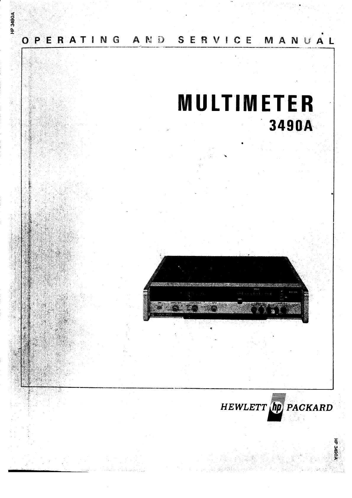
l-2. The Model 3490A Multimeter
makes
ac
voltage,
dc
voltage,
and resistance
measurements
with 5-digit resolu-
tion. It is capable of overrange measurements
up to
l2O% of range
on all except the 1000V ac and dc
ranges.
Polarity selection and display are automatic.
Range
selection is manual or automatic over all ranges
on all functions. Options are available
to provide data
output, remote programming,
sample-and-hold
measure-
ments,
and
ratio measurements.
1-3. This manual contains installation and operating
instructions as well as maintenance
information for the
Model 34904 Multimeter. Instrument specifications
and
procedures
for verifying proper operation are
included.
Procedures
are also included for adjusting the instrument
to its performarice specifications.
Schematic
diagrams,
the theory of operation, and troubleshooting informa-
tion are provided for use
in maintaining
the instrument.
14. This section of the manual contains the perfor-
mance specifications for the Model 3490A and lists the
available options. It also lists the accessories supplied
with the Model 3490A and additional accessories that
are available.Instrument
and manual
identification infor-
mation is also included.
1-5.
SPECTFtCATI0NS.
l-6. Table l-l is a complete list of the Model 3490A
critical specifications
that are controlled by tolerances.
Table l-2 contains
general
information that describes the
operating
characteristics
of the Model 3490A.
l-7. Any change
in the specifications
due to manufac-
turing, design, or traceability to the U.S. National
Bureau of Standards
will be listed on a manual change
sheet
included with this manual.
The manual
and manual
change
sheet
supersede
all
previous
information
concern-
ing specifications
of rhe 3490A.
r-8.
0PT|0NS.
l-9. The following options are available to extend
the
usefulness
of the
Model
3490A:
Option
020:
Option
021:
Option
022:
Option
030:
BCD/Remote
Expand
Isolated
Data
Output (BCD)
Isolated
Remote
Control
(Options
021
and 022
require
Option
020)
General
Purpose
Interface
Bus I/O
(GPrB)
sEcTt0N I
GENERAT INFORMATION
Option 040 or 045: Sample-and-Hold
Option 050: 34904
designed
for operation
on
50
Hz
power
source
Option 060: 3490A
desigred
for operation
on
60 Hz
power
source
Option 080: Ratio
I-Ill. ACCESSORIES
SUPPLIED.
l-ll. The following
accessories
are
supplied
with the
Model 3490A
and its
option as
shown.
Supplied
with
all instruments:
Rack
Mount Kit
PC
Extender
(2 x l8)
Supplied
with Option 020:
Rear input cable
36-pin
connector
(mates
with Remote
connector,
J7)
5Gpin
connector
(mates
with Data
Output connector,
J6)
Remote Jumper
Assembly,
A.4
PC
Extender
(2x22)
Supplied
with Option 030:
l4-pin connector
(mates
with Trigger
connector, Jl l) 12514142
Remote
Jumper
Assembly,
44 0349U66504
Rear input
cable 0349041612
PC Extender (2
x 22) 5060{630
Supplied
with
Option
040:
S/H Analog
Jumper
Assembly,
A24 0349046524
.-' S/H Logic
Jumper
Assembly,
A25 03490-66525
PC Extender (2
x l0) 50606032
Supplied with
Option
045:
S/H Analog
Jumper
Assembly,
A24
S/H Logic
Jumper
Assembly,
A25
PC Extender
(2
x l0)
l4-pin
connector
(mates
with Trigger
connector, Jl l) 12514142
Supplied
with
Option
080:
Ratio
Jumper
Assembly,
A26
PC
Extender
(2
x l0)
1.12.
ACCESSORIES
AVAITABLE.
l-13. Several
accessories
are available
for use
with the
Model 3490A.
A service
video tape, Product
No. 90030C
Option 705, will demonstrate
use
of self-test
and front
panel symptoms
to isolate failures.
The -hp 111261^
accessory provides
a set of IC reference
boards with
1-t
Section I
most of the 3490A logic IC's for use with the -hp
lO529A Logic Comparator. Using these
boards with the
Logic
Comparator,
a
faulty IC can
be isolated
in seconds
without removing it from the circuit. A spare
parts
set,
-hp- 11127A, is available for the 3490A. This set
contains the most critical components
of the 3490A
such as integrated circuits,
transistors
and reed relays.
Three interface cables are available
for the GPIB Option
030. These
cables
are
identical
except
for length.
l063lA Interface
cable,3 ft.
10631B Interface
cable,6
ft.
10631C
Interface
cable,
12 ft.
A GPIB Repair Kit, -hp- Part No. 0349G80009, is
available
for troubleshooting the General
Purpose
lnter-
face Bus I/O circuits.
Also available is a cable. Product
No. 562A-16C,
for use with Option
021 and *rp 50508
or 50554, Printers. Field
installable
Options
O2l and,O22
for units with Option O2O are available by accessory
numbers
Ill2lA and I I l22A respectively.
Model
3490A
1.14.
INSTBUMENT AND
MANUAL
IDENTIFICA-
TION.
l-1
5. Instrument identification by serial number is
located on the rear panel. Hewlett-Packard
uses a
two-section serial number consisting
of a four-digit
prefix and a five-digit suffix separated by a letter
designating the country in which the instrument was
manufactured. (A =
U.S.A.; G
=
West Germany;
J = Japan;U
= United Kingdom.)
l-16. This
manual
applies to instruments
with the serial
numbers
indicated on the title page.
If changes
have
been made in the instrument since this manual was
printed, a "Manual
Changes" supplement
supplied
with
the manual
will define these
changes. Be sure
to record
these changes
in your manual. Backdating information in
Section VIII adapts the manual to instruments with
serial
numbers lower than that shown on the title page.
Part numbers for the manual
and the microfiche copy of
the manual are
also
shown
on the title page.
l-
Model 3490A Section
I
Table
1-1
. Specifications.
DC
VOLTAGE
Full-Rangp
Display: . :1P9P.Y r 10O.oOo
v
i I;IBBBB V .
rooo.öö
v
Overrange: 2O % onall ranges
except
1000
V range
Aeuracy: t l%
of reading + To
of rangel
Temperaturo
Coefficient (0o C to 50o Cl:
O.1 V Range: t (0.00,l
% of reading
range)/o
C
' 1V through 1OOOV
Ranges:
r(O.OO1
Temperature Coefficient l0o C to
reading
+ 0.001
%
of range)F
C
Voltage
Coefficient
(1000V range):
kHz
to % of reading
Input
lmpedance:
2 Mf, t 1 %shunted
by:
( 65
pF
without rear
input
terminal
< 90 pF
with rear
input
terminal
OHMS
Full-Rangs
Display:
.100000
ke
l.oo000 ko
10.0000
ka
100.000
ko
1000.00
ko
10000,0
ko
Overrange:
2O
% on
-all
ranges
Accuracy: + (%
of reading
+ oÄ
of rangel
50P
Cl: r (0.002
% of
Add 0.01
ppm per Volt/
+ 0.OO03
% of rangelp C
Voltage
Coefficient {
I 000 V range)
:
reading.
Effectlve Common{lode Rejoction
either
loadf:
AC:
Option O5O (SO
Hz power
50H2t0.1
%
Option 060 (@ Hz power
6OHzt0.1
%
DC:
) 140dB
AC Normal{Vlode
Rejection
:
Option 05O (5O
Hz power
!O.l%
Option 060 (60 Hz power
to.1 %
Input Resistance:
+ 0.0007 % of
% of reading
Add 0.04 ppm/vott to % of
(with 1 kf,l imbalance in
frequency):
) 140
dB at
frequency):
) 140d8 at
frequencyf:
>S0dB at 50
Hz
frequency):
> 50
dB at 60 Hz
O.1,V
through
10
V ranges
(< 70%
R.H.): > 2 x 10¹⁰
O
100
V
and
lü)0 V ranges:
10
MO
I O.1S
% -
AC
VOLTAGE
Full-Range
Display: I.OOOOO
V
10.0000
v
100.000
v
1000.00
v
20 Hz 50 Hz 100
kHz* 2SO kHz
24 hours
(230
C r 10
cl
3) days
(230Cr50c)
90
days
(230C150C)
6 months
(23()C15()Cl
l ye€r
(230c+5()Cl
I Frequencies greater than
l0 V ranges
only. lO0
kHz specified
on 1 V and
Overrange:
2O%on
all ranges
except
IOOO
V range
ttTlgnt Rango:
20 Hz to 250 kHz (Guard
shorted
to Low),
10' nnximum
Volt-Hertz
product
Accuracy: x l%ot reading
t % of range)
lnput levels
above
1 % of range
Guard
must
be
connected
to Low
Temperature
Coefficient (0o C to 50o C):
0.1 ko range: ! (O.OOI
% of reading +O.OO07
% of
range)P
C
1 kO through t0,0OO
kf,l ranges
(< 70% R.H. on 1OOO
kj_l
and 10,0O-0
kf,!
ranges):
r (O.OO1%
ot reaaint
i O.OOOSX
of range)/"C
DATA OUTPUT
(Optaon
OZtl
BCD 1-2-4€, High
true or Low true logic
code,
selectable
by
internal
sl,rritch
I
nput
Signals
Output
Signals
High Level Low Leval
+3.9Vr1.5V,
100pA
max.
+3.9
V r 1.5
V,
4O0
pA rnax.
+0.3v
t0.3V,
2 mA rnax.
+0.3vr0.3v,
15
mA
max,
REMOTE
CONTROL
(Option
0221
Remote programming
of range
and
function uses
|rigrh
true rogic
code.
I nput
Signals
Output
Signals
High Level Low Level
+3.9Vt15V,
100pA
max.
or
open
circuit
+3.9Vr1.5V,
40O
pA nrax.
+0.3v!0.3v.
2 mA rnax.,
or
contact
closure
to ground
through
< 300
o
+o.3V
r0.3V,
15
mA nnx.
24 hours
{23oc
! loc)
30 days
(23oc1soc)
90 days
(23oc r5()c,
6 months
{23ocisocf
1 year
{23oc!soc)
.1 V Range 1V-f00{,VRangas
t (0.005
+
0.001
)
I (0.01 +
0.005)
! (0.01 +
0.005)
r (0.013
+
0.0051
t (o.015
+
0.0051
(0.004
+
O.OOI
)
(0.008
+
0.0021
(0.01 +
0.0021
(0.013
+
0.oo2l
(o.015
+
0.oo2l
24 hours
(23oc 1
loc)
30 days
(23oc!socl
9O
days
l23oc!50c)
6 months
{23oc t socl
I year
0.006
+
0.001
0.O12 +
o.OOs
0.012
+
o.oo5
o.ot
5
+
0.005
0.018 +
O.OO5
0.005 + 0.001
O.01 +
0.002
0.012
+
0.002
0.0t5 +
0.002
0,018 +
0.002
0.007 +
0.001
o.0t2
+
0.002
0.0'l5
+
0.002
0.02 +
0.002
0.025 +
0.002
0.025
+
0.ool
0.035
+
0.002
0.035
+
0.002
0.04 +
0.o02
o.05 +
0.002
0.32+0.05 lO.oo+0.025 | 0.7 +0.06
0.35+0.05
lo.r +0.025
| o.zs*o.oe
0.35+o.os
lo.t +o.o2s
lo.zs*o.oo
0.4
+0.06 | o.r +0.03 | o.zs*o.oz
0.45+0.07
| o.tz+o.o3s
| 0.7s+o.o8
l-3
Section
IModel 34904
Table
1-1. Specifications
(Cont'd).
RATIO (Option 0801
Ratio Measurement
Input Configuration:
3 wire; External Reference
Low is conlmon with Input Low.
External Reference High may be positive or negative with
respect to Low. I
nput
Ratio
=
Ext. Ref.
External Reference
lnput Resistance: > 107O
DC/DC Measurement
Accuracy: Ext. Ref. Range
! (Ao/o
of Reading
r Bo/o
of lnput Range
+ -
Ext. Ref . Voltage
/
External Reference
Ranges:
1V:1O.1
Vtot1.2V
10V:
tlVto112V
{1 V range should be used
for greater accuracy if the Ext- Ref'
voltage
is between 1 V and 1.2 V.
Input Ranges:
DC: o.1 V to 1000
V
AC: 1 V to 1000
V
xC%of Input Range)
Ext. Ref.
Range
lnput Range
1V 1V,
10V 100
v, 1000
v
ABcABcABc
24 hours
(23"C
I 1"c) tov
1V .003 .001 .oo2
.o03 .002 .002 .002 .001 .oo2
.002 .002 .002 .003 .001 .002
.005 .003 .002
3o days
(23"c r 5"c) 10v
1V .oo7 .005 .0m
.008.015.003 .002 .003 .002
.o03 .012 .003 .005 .003 .002
.006 .o12 .003
9o days
(23"c t s"cl 10v
1V .o07 .oo5 .002
.008 .015 .003 .002 .003 .002
.o03 .012 .OO3 .006 .o03 .002
_007 .01
2 .003
6 months
(23oc r s"cl 10v
1V .007 .005 .002
.008 .015 .003 .002 .003 .oo2
.003 .012 .003 .007 .003 .002
.008 .012 .OO3
1
year
123oc
t 5"c) 10v
1V .o07 .005 .002
.008 .o15 .o04 .003 .o03 .002
.004 .012 .004 .008 .003 .o02
.o09.012.OO4
Notes:
1. On the lOOO
V range, add 0.04 PPM/volt to the %
of reading
specification'
2. EMF's generated external to the 34904 {lay b9 cgmpensated to achieve the % of range
accuracy
specified by utilizing the rear panel
ThermafAdjust provided'
DC/DC Temperature Coeff icient:
! lo/o
of Reading
+ %
of Input Range)/-C
Ext. Ref.
Range
lnput Range
1V 1V,
10V 100
v, 1000
v
'10
v
1V r {0.0003
+ 0.0007}
r (0.0004
+ 0.0021
r (0.0001
+ 0.00041
r (0.0002
+ 0.0021 =(0.0005
+ 0.0004)
(0.0006
+ 0.002)
t
DC/DC Measurement
Accuracy Example:
lnput Voltage
= 0.5 V; Input Range
= 1 V
Ext. Ref.
Voltage
= 0.5 V; Ext. Ref . Range
= 1 V
30 day spec.
= t (0.0037o
of Reading
+ O.O12%
of lnput Range
Ext. Ref. Range
x 0.003% of Input Rangel
Ext. Ref
.
Voltage
Ratio Reading should be 1.00000
0.003% of Reading = 3 counts
O.O12% of Input Range : 12
counts
* x o.oos"Ä of Input Range= 6 counts
.5V
Total rror tolerance = 21 counts
Display should be
0.99979
to 1.00021
AC/DC Measurement Accuracy :
10 V Ext. Ref. Range: Same
as
AC Voltage aocuracy
1 V Ext. Ref.
Range: ^
24 hours 123-C t 1-C)l Same^as
AC Voltage accuracv
30 davs to 1 year Q3-C x 5-C): Add o.01 to % of Rang
AC Voltage accuracy
{See
Table
1-1 of main
34904 manual.l
AC/DC Temperature Coeff
icient:
10V Ext. Ref. Range: Same as AC Voltage temperature
coefficient
1 V Ext. Ref. Range: Add 0.001 to o/o
ol Range in AC Voltage
temperature coeff icient specif
ication
(See
Table 1-1
of main 3490A manual.)
tt
t-
Table
1-1.
Specifications
(Cont,d.)
SAMPLE/HOLD
(OPtion
040/0451
Full-range
Display: Sample/Hold
Measurement
Accuracy (DC
function, I V through
1ü)0 V ranges!:
r 1.00fi) v
+ 10.q)0
v
! 100.00
V
r 1000.0
v
24
hours
(23o
c r 10
c)
30.days
(23o
c r so c)
90 days
(23o
c r so
c)
6
months
(239
C r So C)
1 year
1230 c r so cl
t (% of reading + oÄ
oI rcngel
Sample/Hold measurement
displar/
is
4 full
digits plus overrange
"1 ",
r {0.01
+0.0151
r (0.01
+
0.015)
r (O.01
+
0.015)
r (0.02
+
0.0151
I (o.02
+
0.015)
50o
C)r t !O.OO2 % ol
Ovrrangs: 2O%on all
range5
except
IOOO
V range. Temperature Coefficient (04 C to
reading
+ 0.0O1 % of range/o C).
Model34904
Maximum Input Voltages:
Between Input High and Low: t 10O0
Vrms (1 1500 V peak)
Between
either Low terminal and Guard: I 200 V
Between
Guard and Chassis:. 4 500 V
Between O Signal High and Low: t 250 Vrms
Range
Seleaion: Manual,
autornatic, or Remote (Optionall
Maximum Reading
Rate (Minimum Sample periodr per Readingl:
Function Option
050 Option
060
DC
Volts
AC
Volts
Ohms
.1 kto
100
k
1,000
k
10.oo0
k
240.2ms+5ms
1.26s
+ .025s
24O.2ms+5ms
3O0.2ms+6ms
66O.3 ms
+ 12
ms
200.1
ms+4ms
1.05s
+ .025s
20O.1
ms+4ms
250.1
ms+5ms
55O.2
ms
* 10 ms
'Sample Rate Control set to FAST position and instrument
not in owrload.
Response
Time (to within rated accuracy for a step input applied
coincident with encode
triggerl:
DC Volts: ( 200 ms
ACVolts: <lsecond
Ohms:
0.1 k to 100 k ranges: ( 200 ms
10O0
k range: ( 2S0 ms
10,OO0
k range: ( 5SO ms .:
Ohms Terminal CharacteristiG3:
Maximum voltage
across
unknown resistance:
25 V in overload
1 3 V for valid reading
Nominal current through unknown resistance:
O.1
k to 10 k ranges: .l mA
100 kand 1000 k ranges:
10
pA
10,000krange: l rtA
Overload protection:
Nondestructive: r 2SO
V
Fusedestructive: r 10OOV
Power Raquirements:
10o v, 120 V
,22O V
, or 24O
y l+ 5 %, - 1O %l; 48 Hzto 44O Hz
Power Consumption: <60 VA with all options
Environmental Characteristics:
Operating Temperature: Oo
C to 5Oo
C
Humidity Range: ( g5 % relative humidity, Oo C to 4Oo C
Storage
Temperature: - 2Oo
C to + 75o C
Section
I
Table 1-2. General
Information.
GENERAL PURPOSE
INTERFACE BUS (ourguard)
ground is
isolated from inguard circuit common (input Low terminal!
and chassis {power tine) ground and may be floated a
maximum of 40 V above
chassis.
SAMPLE/HOLD
Acquisition Time (Settling tam6 for a f ult+ange slep inputl:
GENERAL
PURPOSE
INTERFACE
BUS
LOGIC
LEVELS
All lines are LOW true except HRFD and HDAC, which are
HIGH
true.
Input Signals:
Each
input line is terminated
with 3 kslto + S V and
6.2 ke
to ground,
and
one
TTL load.
Output Signals:
Each output can drive 15 GplB loads. The output is an
open-collector driver capable of sinking 4g mA at 0.4 V
out-
Maximum
Acquisition Time
to
Range within 0.Ol %
of Final
Value
Aperture Time (Delay betwsen
the time a Sample/Hold
Trigger
/'' command h receiwd and the time Amplifier A entors the
Hold
model:
Track/Hold: ( 400 ns (typically 22O nsl; cVcle-to_clrlcle
vari-
ation<t10ns.
Acquire/Hold:
1V, 100 V ranges 615 rls t 4O0 ns 512.6 lls r zl00 ns
10 V, 1000 V ranges 154 6 t 40O ns 129.4 tts t 4OO
ns
Sample/Hold Trigger I nputs:
$Tp]9/!9!d TTL Trisser (dc coupted): lnput must go from
HIGH ()+ 2.4 V) to LOW {<+ 0.4 V} for at teast
30 ns.
Signal must be HIGH at least
600 ps prior to going LOW.
Must be
capable
of sinking I mA.
Sample/Hold AC Trigger (ac
coupled): Negative-going
leading
edge of a pulse at least 30 ns wide and having an
amditude of 2 V to 2O0 V. Signal must be stable at least
2 1ts
Drior to negtive-going transition.
l-5
Model
34904
Section
I
Table
1-2. General
lnformation
(Cont'd.)
SAMPLE HOLD (CONT'DI
Sample/Hold AC Characteristics:
Maximum rate of change of input voltage to maintain
tracking:
2.5 %
of range/ps on the 10 V and 1 0OO
V ranges.
5 % of range/prs
on the 1 V and 10O
V ranges.
Maximum dV/dt during digitization: 50 V/t s
Minimum ! 3 dB Bandwidth (external input terminals to
Samde/Hold amplifiersl :
dVs/u
Range
1V
10v
100
v
1000
v
RATIO
Range
Selection:
K1 = Velocity factor. The typical factor for each
range
is as
follows,
Slope of signal as measured in increments
small enough that the waveform between
measurement points approaches
or achieves
linearitV.
Typical VelocitY Factor
Time Response Characteristics :
The time response
of Sample/Hold for any input wave-
form can be approximated by the equation:
-
10,rs
- 2,rs
- 3ps
+7tts
External Reference
Range: Manual
lnput Range: Manual.
automatic,
or remote (optionall
Ratio Display:
1 V Ext. Ref
. Range: Read
ratio directly
10
V Ext. Ref.
Range: Multiply display
bv 0.1
Polarity Display {automatic) :
+ for +DC/+DC or -DC/-DC
_
for +DC/-DC or _DC/+DC
No polarity disPlaY
for AC/DC
Ratio Measurement CaPabilitY :
Maximum Numerical
Display: 1 20O0O
on any Input range
Maximum lnput Voltage: 10O0
Vrms
Maximum Reading
RaE:
DC/DC: Same
as
for dc volt'age
measurements
AC/DC: Same
as
for ac voltage
measurements
Input Protection: 250 Vrms (t 400 V peak)
continuous
Environmental Requilements:
O:C
to 4o:c, ( 95%
relative
humiditY
O"C
to 5O"C maximum operating temperature range
Range
1V
10v
100
v
1000
v
r 3 dB FrequencY
20 kHz
4O
kHz
15 kHz
20kHz
dvin
vs/n
=
vin
+
Kl _f,r
Similarlv, the input waveform can be reconstructed
from
measured data by the equataon:
vin =
vs/H -
rl dvs/H
dt
Where:
VS/n = Displayed Sample/Hold measurement.
Vin = 39OA input voltage.
dVi. Slope
of any portion of an input wavefori?i.
dt
t-6
Model3490A
SECTION
INSTATI.ATION AN
D
Section
II
tl
INTERFACE
Figure
2-1
. Line Voltage
Selection.
appropriate receptacle,
grounds the instrument. The
offset pin on the power
plug is the ground
connection.
2-12. To preserve
the protection
feature
when
operating
the instrument
from a two+ontact outlet, use a three-
contact
to two-contact
adapter
and connect
the
wire on
the
adapter
to power-line ground.
2-13. The 349OA power cord, power input receptacle
and mating connectors
meet the safety standards
set
forth by the Intemational
Electrotechnical
Commission
,(rEc).
2.14.
ENVIRONMENTAL
REOUIREMENTS.
2-15. The Model 3490A requires no special
cooling
equipment if the instrument is mounted to allow free
flow of air around
all surfaces.
The instrument
may be
operated
where the ambient temperature
is between
0o
C and 40o C and the relative humidity is less than
95 %. The instrument may be stored at temperatures
between
- 20o
C
and
+ 75o
C.
8r20-1689 8t20-r369 8120-t35t 8t20-r348
"'i,nur"
2-2. Powercord
Gonfigurations.
2.r.
|NTR0Dt
CTloN.
2-2. This section contains
information and instructions
necessary
for installing and
interfacing the Model 3490A
Multimeter. Included are initial inspection procedures,
power and
grounding
requirements, environmental
infor-
mation, installation instructions,
interconnection
pro-
cedures,
and instructions for repackaging
for shipment.
2.3.
INITIAL
INSPECTION.
2-4. This instrument was carefully inspected both me-
chanically and electrically before shipment.
It should
be
free of mars or scratches
and in perfect electrical order
upon receipt. To confirm this, the instrument
should
be
inspected
for physical damage incurred in transit. If the
instrument was damaged in transit, file a claim with the
carrier. Check for supplied
accessories
@aragraph
1-10)
and test the electrical performance of the instrument
using the performance test procedures outlined in
Section V. If there is damage or deficiency, see the
warranty in the front of this manual.
2.5. POWEB
REOUIREMENTS.
24. T\e Model 3490A
can
be
operated
from any
power
source
supplying
100
V, l2OV, 220
Y or 24O
V (- l0 %
+ 5V),48H2 to 44OHz.
Power
dissipation
is 60VA
maximum. Refer to Paragraph
3-18 (Section III) for
instrument
tum-on procedure.
2-7. Before connecting ac power to the 3490A, make
sure the rear panel line selector switches are set to
correspond
to the voltage
of the available power line as
shown in Figure 2-l . Also, be sure the proper fuse is
installed.
2.8. POWER
CORDS
AND
RECEPTACLES.
2-9. Figure 2-2 illustrates
the standard
configurations
used
for -hp-
power
cords. The
-hp-
part
number
directly
above
each
drawing
is the part number for an instrument
power
cord
equipped
with a connector
of that configura-
tion. If the appropriate
power
cord is not included
with
the instrument,
notify the nearest
-hp-
Sales
and
Service
Office
and
a replacement
cord
will be
provided.
2.1
(|.
GROUNDING
REOUIR
EMENTS.
2-11. To protect operating personnel, the National
Electrical Manufacturer's
Association
(NEMA) recom-
mends
that the instrument
panel
and cabinet
be
ground-
ed. The Model 34904 is equipped
with a three con-
ductor power cable which, when plugged into an
r- IOOV--r
I r-r 20v-l
ilil
I Lzqov----l
\-22OV '
IOO
Volts
r- l@V-
I a rzov-l
ilE
I L zqov--]
L 220V '-
220 Volls
-1O%,+
5% of nominal
90 to 105
volts
108
to 1 26 volts
198 to 231 volrs
216 to 252
volrs
@ffiW
sT0
2-1
Section
II
2.16.
INSTALLATION.
2-17. Bench Use.
2-18. The Model
3490A is shipped
with plastic
feet and
tilt stand
in place, ready for use
as a bench instrument.
The front of the instrument may be elevated for
convenience
of operating and viewing by lowering the
tilt stand. The plastic
feet are shaped
to permit placing
the instrument on top of other full-module Hewlett-
Packard
instruments.
2-19. Rack
Mounting.
2-20. The Model
3490A
may
be rack
mounted using the
rack mount kit (-hp- 0349G84401) supplied with the
instrument. Instructions are included with the kit. The
rack mount is an
EIA standard
width of 19
inches. When
mounted using the rack mount kit, additional support
must be provided at the rear of the instrument. The
dimensions of the Model 3490A
are shown
in Fizure
2-3.
Figure
2-3. Model 3490A Dimensions.
2.21. INSTALLATION
OF OPTIONS.
2-22. T}te Isolated
Data Output (BCD) Option 021
and
the Remote Option 022 may be installed
in the Model
349OA only if the instrument was equipped at the
factory with the BCD/Remote
Expand
Option 020.
2-23.
lsolated
Data
0utput
0ption 021
(-hp-
111ZlAl.
l-24. Use the following procedure for installing the
Isoiated
Data
Output. If the Isolated
Remote
option is
to be installed
at the same time, refer
also to Paragraph
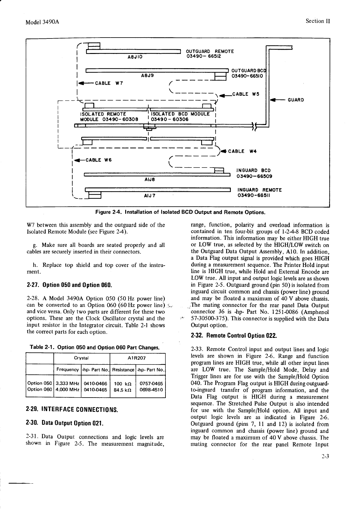
a. Remove
top cover
and shield from the 3490^.
b. Remove
screws
holding cover plate
to instrument
s:rard. This plate is located in left rear portion of
rnsrrument
between
the Inguard
Motherboard
Al and
Out suard
llotherboard
A8.
Model 3490A
c. Install 03490-60306 Isolated
BCD
Module in the
right opening in the instrument guard using screws
provided (see
Figure 2-4).
d. If Isolated Remote (lll22L) is not installed
at
this time, install cover plate
03490-04117
over the left
opening in the guard. If Isolated Remote is to be
installed,
place
the 03490-60308
Isolated
Remote
Mod-
ule in the opening to the left of the BCD
Module (see
Figure
24).
e. Insert the Isolated BCD Inguard PC Assembly
0349U66509 into Connector AlJ8 and install
Cable W4
between this Assembly and the inguard side of the
Isolated BCD
Module
(see
Figure
24).
f. Insert the Isolated BCD Outguard
PC Assembly
03490-66510
into Connector A8J9 and
install
Cable
W5
between this Assembly
and the outguard side of the
Isolated BCD
Module
(see
Figure 2-4).
g. Make sure all boards are seated properly and all
cables
are securely inserted
in their connectors.
h. Replace
top shield and top cover
of the instru-
ment.
2-25. f
solated
Bemote 0ption 022
(-hp-
11122A1.
2-26. Use the following procedure for installing the
Isolated
Remote option. If the Isolated
Data Output
option is to be installed
at the same time, refer also to
Parugraph2-23.
b.- Remove screws
holding cover plate to instrument
guard.
This plate is located
in left rear portion of the
instrument between the Inguard
Motherboard
Al and
the
Outguard Motherboard
A8.
c. Install 03490-60308
Isolated
Remote Module in
the left opening in the instrument guard
using screws
provided
(see
Figure
2-4).
d. If Isolated BCD (11121A)
is not installed
at this
time, install cover plate 03490{4117 over the right
opening in the guard.
If isolated BCD
is to be installed,
place the 03490-60306 Isolated BCD Module in the
opening
to the right of the Remote
Module
(see
Figure
24).
e. Remove the 03490-66504 Inguard Remote Jump-
er Board ard insert the Isolated Remote Inguard PC
Assembly
0349U66511 into Connector AlJT and
install
Cable
W6 between
this assembly
and
the inguard
side of
the Isolated
Remote Module
(see
Figure
2-4).
f. Insert
the Isolated
Remote Outguard PC
Assembly
0349046512 into Connector A8J10 and install Cable
OIMENSIONS IX INCHES
ANO MILLIMETERS
I
(9r.4)
T_
(F
I OUTGUARD REMOTE
03490-
665t2
A8J
IO
I aa,rs 03490-66510
l<- cABLE
w7 / - -
f--- .
TSoLATED
REMOTE : ISOLATED BCD MODULE
MOOULE
03490- 60308 | 05490 - 60306
r-l
rffi l_J I
| -J- --\
I'
I ;+CABLE W4
i . ___/
;<-caBLE rY6
t\
- E TNGUARD BcD
JJiJV-99JWt
AI.J8
-_ f-1 AIJ
7 03490-56511
Figure 24. Installation of lsolated BCD
Output
and Remote Options.
Model3490A
2-29. INTERFACE
CONNECTIONS.
2-30.
Data
0utput
0ption
021.
2-31. Data Output connections and logic
shown in Figure 2-5. The measurement
W7 between
this assembly
and
the outguard
side
of the
Isolated
Remote Module
(see
Figure 24).
g. Make sure all boards are seated
properly and all
cables
are
securely
inserted in their connectors.
h. Replace top shield and top cover
of the instru-
ment.
2-27.
Option 050 and
Option 060.
2-28. A Model 34904 Option 050 (50 Hz power
line)
can be converted
to an Option 060 (60 Hz power
line) ;^.
and vice
versa.
Only two parts
are different for these two
options. These
are the Clock Oscillator
crystal
and the
input resistor in the Integrator
circuit. Table
2-1
shows
the
correct parts
for each option.
Table
2-1. Option 050 and
Option 060 Part
Changes.
Crystal A'1R207
Frequency hp- Part No Resistance +lp- Part No
Option 050
Option 06O 3.333 MHz
4.000
MHz o4100466
0410{465 100 kfi
84.5 ko
07574465
0@8-4510
Section
Il
range, function, polarity and overload information is
contained in ten four-bit groups
of l-248 BCD coded
information. This information may be either HIGH true
or LOW true, as selected
by the HIGH/LOW switch on
the Outguard
Data Output Assembly,
Al0. In addition,
a Data Flag output signal is provided which goes
HIGH
during a measurement
sequence.
The Printer Hold input
line is HIGH true. while Hold and External Encode are
LOW true. All input and
output logic levels are
as
shown
in Figure 2-5. Outguard ground (pin 50) is isolated from
inguard circuit common and chassis (power
line) ground
and may be floated a maximum of 40 V above chasis.
._.The
mating connector for the rear panel Data Output
connector J6 is -hp- Part No. 125l{086 (Amphenol
Output option.
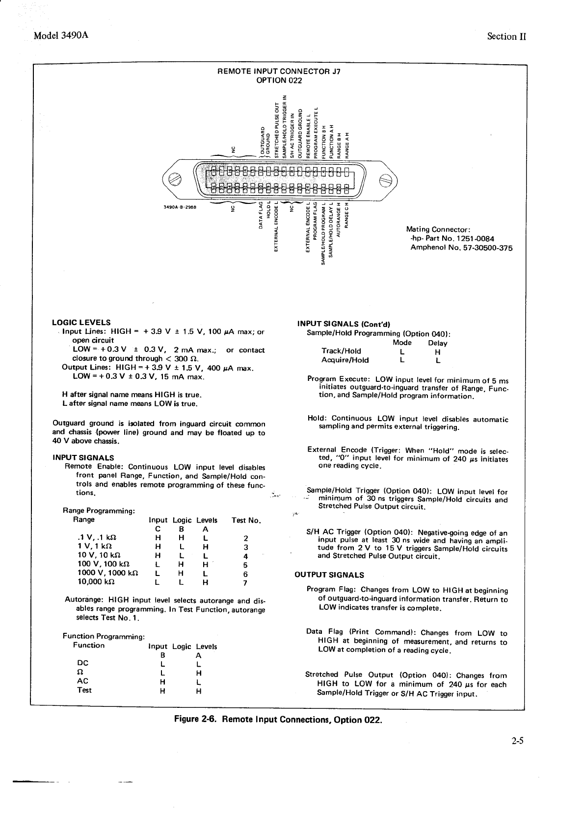
2-32. Remote
Gontrol
0ption 022.
2-33. Remote
Control input and
output lines
and logic
levels are shown in Figure 26. Range and function
program
lines are HIGH true, while all other input lines
are LOW true. The Sample/Hold Mode, Delay and
Trigger lines are for use with the Sample/Hold
Option
040. The Program Flag output is HIGH during outguard-
to-inguard transfer of program information, and the
Data Flag output is HIGH during a measurement
sequen@. The Stretched
Pulse
Output is also
intended
for use with the Sample/Hold option. All input and
output logic levels are as indicated in Figure 2{.
Outguard
ground (pins 7, ll and 12) is isolated
from
inguard
common and chassis
(power line) ground and
may be floated a maximum
of 40 V above chassis. The
mating connector for the rear panel Remote Input
levels are
magnitude,
:-J
Section
II
7N i 3i -s t**
{JrJ
ü,1t;
Model34904
TA OUTPUT
COTruECTOR
.IO
oPTtoN
021
z9
:! z
;9eFe
22
:
qi
äF cö
i: ^j3
Ed
6s
ä
996<
,^j
-8
=:==
8885
Mating
Connector:
-hp-
Part
No. 1251€086
Amphenol No. 57-30500-378
?ä;-;03":'
Y
3 EKBö ?
laEFä=;
;
g
iää
5
LOGIC
LEVELS
Output
Lines:
HIGH
=
+
39 V t 1.5 V,4OO
pA rnax.
LOW
= + 0.3
V r 0J V, lS mA rnax.
Input
Lines:
HIGH
=
+
3.9
V a 1.5 V, 10O
rrA
max.
LOW
=
+O.3
V r O.3
V, 2 mA rnax.
High
Reference
= + 5.3 V
Low Referenc€
{ V - Outguard ground
H
after
signal
name
means
HIGH
is true.
L after signal
narne
means
LOW
is
true.
Outguard ground is isolated from inguard circuit common
and-
chassis
(power linel ground and ,nay be floated up ro
40 V above
chassis.
DATA FLAG (Print
Command
Outputl
Changes
from LOW
to HIGH
at beginning
of measuremenr
and
returns
to LOW
at completion
of a reading
rycle,
PRINTER
HOLD
HIGH input le\rel causes
349OA to stop autornatic
sampling
until level
returns
to LOW.
HOLD
Continuous
LOW input tevel
disables
autornatic
sampling
and
permits
external
triggering.
EXTERNAL
ENCODE
(Trigser)
When
"Hold" mode is selected,
LOW input le\rel
for
minimum ol 24O
ps initiates
one reading
cycle. See
Paragraph
364.
DIGITAL RECORDER
PRTNT
CODES
(Using
-hp-
50508
Standard * or - 1248
print
Wheell
Printer columns
numbered
from right to left. columns 1 through 5 print numerical
value
of measurement.
coded output
information may be either HIGH i.u" or LOW true, as selected
by t'he
HIGH/LOW
switch on the Outguard
Data
Output
Assenilclv,
410' This
switch
must
be
set to correspond
to the
logic
trr" inprt levei
required
by the digital
recorder
used.
Colqmn 6Column
FüfFtkh
HIGH Tre LOü Tr{
Fundid 8it
DCBA Print Fundion 8it
DCBA Pr&rt
O, Remlo
AC, R.mt€
T6,R.@E
DC. F.tio
Jl, R.tio
{nor Elidl
AC, F.r'o
TH, Ratio
oc
o
AC
T6
LH
LH
LHHL
LHHH
HLLL
H
LLH
H
LH
L
HLHH
HHLL
HHLH
HHHL
HHHH
8
9
+
H
LH
L
H
LLH
HLLL
LHHH
LHHL
LHLH
LHLL
LLHH
LLHL
LLLH
LLLL
6
7
8
9
+
N6
Dkplay
HlcH Tru. LOW Trü.
Data
OCBA Print Dat€
DCBA Ptint
0LLLL
LLLH 0
I
LLLH
LLLL
Colomn t
O.ta
Multiplit
HIGH Tru. LOW
Tru.
Ragr 8ir
DCBA Print Rangr Bir
OCBA Print
to-r
to-2
to-3
to{
to€
'to€
LLLH
LLHL
LLHH
LHLL
LH
LH
LHHL
'|
2
4
5
LHHL
LHLH
LHLL
LLHH
LLHL
LLLH
o
o
T,i",,*
lJ.
i: f: ,1.:
,t;:
;
Cdumtr I
Polrity,
Onrlod
HIGH Tru. LOIV Tru!
D.b
DCEA Print O.b
DCBA Print
+
+,
OL
-.
oL
LLLL
LLLH
LLHL
LLHH
o
1
2
LLHH
LLHL
LLLH
LLLL n
DaE raG Data Multiplier giv6 nesurerent an rclB or
kilohG ex@Fit
for Ratio |@iuEments.
Column
g
Column l0
S..tipb/Hold
Mode
HIGH Tru. LOW Tre
D.b
DCEA P.int Dü
DCBA Print
ON
OFF HLHH
HHHH HHHH
HLHH 4
Fundid
HIGH True LOW Tru€
Function Bit
DCBA Print Functioo 8il
DCAA Print
DC,
Re@te, Ratio
tl, BemG, Ratio
AC, Remre, Ratio
T6t, Rmte, Rario
OC, Remre
LLLL
LLLH
LLHL
LLHH
LHLL
0
I
2
4
HHHH
HHHL
HHLH
HHLL
H
LH
H
0
1
3
4
l-r
Figure
2-5. Data Output Connections,
Option 021
.
Model34904 Section
II
FE
lo
rE=ä;:
e
t:uE3X:I--
52 H *
F
E I =
6 s
i ä
" qd E
; ?
3 5 fr i F 3 ä
2- 39H;;5EEiF==
34904-B-296a
LOGIC LEVELS
. lnput Lines: HIGH = + 3.9 V t 1.5 V, 100 pA rnax;
or
open circuit
LOW = + 0.3 V I 0.3 V, 2 mA rnax.; or contact
closure to ground through < 300 A.
Output Lines: HIGH = + 39 V j i.S V, 400 pA nnx.
LOW
= + 0-3 V 1 0.3 V, 15 mA max.
H after signal name means HIGH is true.
L after signal
name means LOW is
true.
Outguard ground is isolated from inguard circuit common
and chassis (power linel ground and may be floated up to
40 V above chassis.
INPUT SIGNALS
Remote Enable: Continuous LOW input level disables
front panel Range,
Function, and Sample/Hold con-
trols and enables remote programming of these func-
tions.
Range Programming:
Range lnput Logic Levels Test No.
CBA
.1 V,.1 ksl H H L 2
lV,
1KO H L H 3
10v,
10ko H L L 4
100v. 100ko L H H 5
1000v,1000ko L H L 6
10,000ko L L H 7
Autoränge: HIGH input level selects
autorange and dis-
ables range programming. In Test Function. autorange
selects
Test
No. 1.
Function Programming:
Function Input
B
DCL
'rlL
ACH
Test H
Logic Levels
A
L
H
L
H
REMOTE INPUT
CONNECTOR J7
oPTtoN 022
Mating Connector:
-hp-
Part
No. 1251
{O84
Amphenol No. 57-3Ob00-37S
INPUT SIcNALS (Cont'd)
Sample/Hold Programming (Option O40):
Mode Delay
Track/Hold L H
Acquire/Hold L L
Program
Execute: LOW input level
for minimum of 5 ms
initiates
outguard-to-inguard
transfer
of Range,
Func_
tion, and
Sample/Hold
program
information.
Hold: Continuous LOW input level disables
autornltic
sampling and permits external triggering.
External Encode (Trigger: When ,,Hold,, mode is serec_
ted, "0" input level for minimum of 24O ps initiates
one reading
cycle.
Sample/Hold Trigger (Option O4O): LOW input levet
for
.*' minirpum of 30 ns triggers Sample/Hold circuits and
Stretched Pulse
Output circuit.
iL.
S/H AC Trigger (Option 040): Negativegoing edge of an
input pulse
at least
30 ns wide and having
an ampli-
tude from 2 V to 15
V triggers
Sample/Hold
circuits
and Stretched Pulse
Output circuit.
OUTPUT SIGNALS
Program
Flag: Changes
from LOW to H|GH at beginning
of outguard-to-inguard information transfer. Return to
LOW indicates
transfer is
complete.
Data Flag (Print Commandl: Changes from LOW to
HIGH at beginning
of measurement,
and returns to
LOW at completion of a reading
cycle.
Stretched Pulse Output (Option 04Ol: Changes from
Hf
GH to LOW for a minimum ot 24O tts for each
Sample/Hold Trigger or S/H AC Trigger input.
ä-j=!9il
äEHäEä
t:Litr
EF!!A
= Ir
* qc
- .<
=a
*
Figure
2-6. Remote
Input Connestions,
Option 022.
2-5
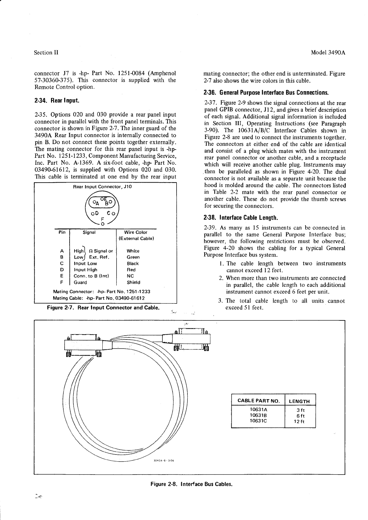
Section
II
connector J7 is -hp- Part No. l25l{084 (Amphenol
57-30360-375). This connector is supplied with the
Remote
Control
option
2-34. Rear
Input.
2-35. Options 020 and 030 provide a rear
panel
input
connector
in parallel
with the front panel
terminals. This
connector is shown
in Figure 2-1
. The inner guard
of the
3490A Rear Input connector is internally connected
to
pin B. Do not connect these
points together externally.
The mating connector for this rear panel input is -hp-
Part No. 125l-1233, Component Manufacturing
Service,
Inc. Part No. A-1369. A six-foot cable,
-hp Part No.
03490-61612, is supplied with Options 020 and 030.
This cable
is terminated
at one end by the rear input
Model 3490A
mating
connector; the other
end
is unterminated.
Figure
2-7 also shows the wire colors
in this cable.
2-36.
General
Purpose
lnterface
Bus
Connections.
2-37
. Figure
2-9 shows the signal connections
at the rear
panel
GPIB connector, Il2, and.
gives
a
brief description
of each
signal. Additional signal information is included
in Section III, Operating Instructions (see
Paragraph
3-90). The 1063IA/B/C Interface Cables shown in
Figure
2-8 are
used to connect
the
instruments
together.
The connectors
at either end of the cable
are
identical
and consist
of a plug which mates with the instrument
rear
panel
connector
or another cable, and a receptacle
which will receive
another cable
plug. Instruments may
.then be paralleled
as shown
in Figure
4-20. The dual
connector
is not available as
a separate
unit because
the
hood is molded
around the cable.
The connectors
listed
in Table 2-2 mate with the rear panel connector or
another cable. These
do not provide
the thumb screws
for securing
the connectors.
2-38.
Interface
Gable
Length.
2-39. As many as 15 instruments can be connected
in
parallel to the same General
Purpose Interface bus;
however,
the following restrictions must be observed.
Figure 4-20 shows the cabling for a typical General
Purpose
Interface
bus system.
l. The cable length between two instruments
cannot exceed 12 feet.
2. When
more
than two instruments
are
connected
in parallel,
the cable
length to each additional
instrument
cannot
exceed
6 feet
per
unit.
3. The total cable length to all units cannot
exceed 5 I feet.
A
B
c
D
tr
r
Rear Input Connector,
J10
Signal
)
High\ o Sisnal
or
LoryJ Ext. Ref.
Input Low
Input High
Conn. to B (lnt)
Guard
Wire Color
(External
Cable)
White
Green
Black
Fled
NC
Shield
Mating Connector: -hp-
Part No. 1251-1233
Mating
Cable: -hp-
Part No.03490-61
612
Figure 2-7. Rear Input Connector and Cable.
CABLE
PART
NO. LENGTH
10631A
106318
10631C
3ft
6ft
'l2tt
Figure
2-8. Interface Bus Cables.
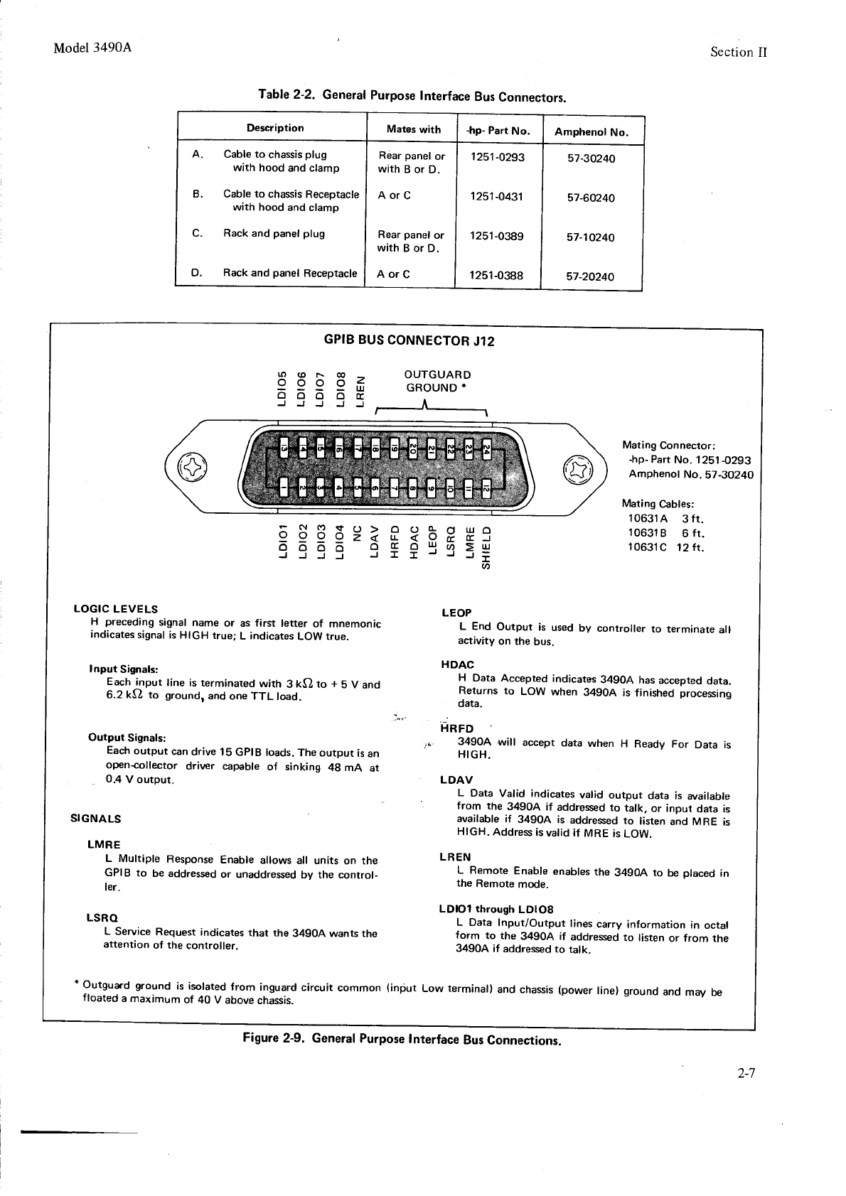
Model
3490A Section
II
Table
2-2. General
Purpose
Interface
Bus
Connectors.
Description Mates
with -hp-
Part No. Amphenol No.
A.
B.
a
D.
Cable to chassis
plug
with hood and clamp
Cable to chassis Receptacle
with hood and clamp
Rack
and
panel plug
Rack and panel Receptacle
Rear
panel
or
with
B or
D.
AorC
Rear
panel
or
with
B or
D.
AorC
1251-0293
'1251-0431
1
251
-0389
1
251
-0388
51-30240
57-60240
57-10240
57-20240
GPIB
BUS
CONNECTOR
Jl2
OUTGUARD
GROUND
*
ro(oF@
9999f
n^^A
JJJJJ
8ä;;'iEFq8ä+
6
Mating Connector:
-hp-
Part
No. 1251
4293
Amphenol No.57-3O24O
Mating Cables:
10631A 3
ft.
10631
B 6 ft.
10631C 12
ft.
LOGIC
LEVELS
H preceding signal name or as first letter of mnemonic
indicates
signal
is HIGH true; L indicates LOW true.
Input Signals:
Each input line is terminated with 3 kO to + 5 V and
6.2 kO to ground, and one TTL load.
Output Signals:
Each
output can drive 1
S GPI
B loads.
The output is
an
open{ollector driver capable of sinking 4g mA at
O.4
V output.
SIGNALS
LMRE
L Multiple Response
Enable allows all units on the
GPIB to be addressed
or unaddressed
by the control-
ler.
LSRO
L Service Request indicates that the 34904 wants the
attention of the controller.
LEOP
L End Output is used by controller to terminate all
activity on the bus.
HDAC
H Data Accepted indicates 34904 has
accepted data.
Returns to LOW when 34904 is finished processing
data.
HRFD
HIGH,
LDAV
L Data Valid indicates valid output data is available
from the 34904 if addressed
to talk, or input data is
available if 3490A is addressed
to listen and MRE is
HIGH. Address
is
valid if MRE is LOW.
LREN
L Remote Enable enables
the 34gOA to be placed in
the Remote mode.
LDIO1 through LDIOS
L Data Input/Output lines carry information in octal
form to the 34904 if addressed
to listen or from the
3490A if addressed
to talk_
'Outguad ground is isolated from inguard circuit common (input Low terminall and chassis
(power linel ground and may be
floated a maximum of 40 V above
chassis.
Figure
2-9. General Purpose
lnterface
Bus
Connections.
a1
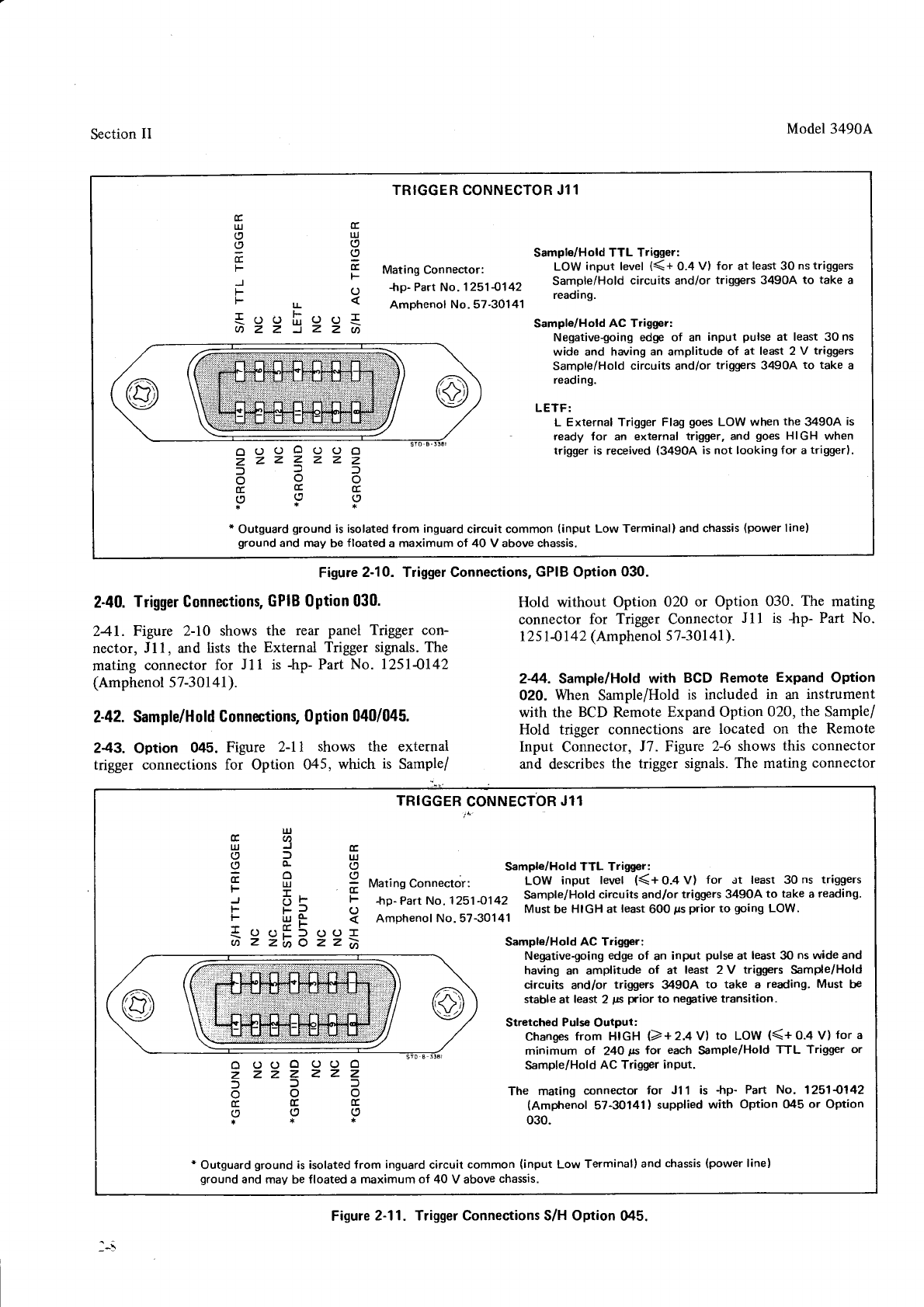
Section
II
2-40.
Trigger
Connections,
GPIB 0ption 030.
241. Figure 2-10 shows the rear panel Trigger con-
nector, Jll, and lists the External Trigger signals. The
mating connector
for Jll is -hp- Part No. 12514142
(Amphenol 57-30l4l).
2-42.
Sample/Hold
Connections, 0ption
040/045.
243. Option 045. Figure 2-ll shows the external
trigger connections for Option 045, which is Sample/
Model 3490A
Hold without Option 020 or Option 030. The mating
connector
for Trigger Connector
Jll is {rp- Part No.
1 25 1 41
42
(Amphenol
57-301 4
I
).
2-44. Sample/Hold
with BCD Remote Expand Option
020. When Sample/Hold
is included in an instrument
with the BCD Remote
Expand Option
020,
the Sample/
Hold trigger connections
are located on the Remote
Input Connector,
J7. Figure 2-6 shows
this connector
and describes
the trigger signals.
The mating
connector
TRIGGER CONNECTOR Jl1
E
UtJJE
!2 lg
9V
=g
FCE
JF
-v
FL
L
;22399ä
Mating Connector:
*rp- Part No.
1251.0142
Amphenol
No.57-30141
zZ
l
tr
* Outguard ground is isolated from inguard circuit common (input Low Terminal) and chassis
(power line)
ground and may be floated a maximum of 40 V above chassis.
Sample/Hold TTL Trigger:
LOW input level
((+ 0.4 V) for at least 30 nstriggers
Sample/Hold circuits and/or triggers 34904 to take a
reading.
Sample/Hold AC Trigger:
Negativegoing edge of an input pulse at least 30 ns
wide and having an amplitude of at least 2 V triggers
Sample/Hold circuits and/or triggers 3490A to take a
reading.
LETF:
L External Trigger Flag goes LOW when the 3490A is
ready for an external trigger, and goes HIGH when
trigger is received (34904 is not looking for a triggerl.
ooooo
zzzzz
6ö
E6
(9c,
t*
Figure
2-10. Trigger Connections,
GPIB
Option
030.
EA
IlJIE
\:/JIU
oclo
no(,
F=F
) ol F
!- t-? ()
: HF
*o(JifC)(Jr
ui
z z'@O zzAi
TRIGGER
CONNECTbR
Jl1
Sample/Hold TTL Trigger:
Mating Connector: LOW input level {(+ O.4
V) for .)t least 30 ns triggers
+rp_
part No. 1251*,142 Sample/Hold circuits and/or triggers 34904 to take a reading.
Amphenol No.57-30141 Must
be HIGH at least
60o ps prior to going
Low'
Sample/Hold AC Trigger:
Negative-going
edge of an input pulse
at least 3()
ns wide and
having an amplitude of at least 2 V triggers Sample/Hold
circuits and/or triggers 3490A to take a reading. Must be
stable
at least
2 ps prior to negtive transition.
Stretched Pulse
Output:
Changes
from HIGH l2+z.q V) to LoW ({+ o.+ V) for a
minimum ot 24O tts
for each Sample/Hold TTL Triggpr or
Sample/Hold AC Trigger input.
The mating connector for Jl 1 is *tp- Part No. 1251{142
(Amphenol 57-30141) supplied with Option 045 or Option
030.
z
lzz oooo
2ZZZ
--
A
ai ,4
**
* Outguard
ground
is isolatedfrom inguard
circuit
common (input Low Terminalland chassis
(power
linel
ground and may be floated a maximum of 40 V above
chassis.
Figure
2-11. Trigger Connections S/H Option
045.
Model3490A
for J7 is -hp- Part No. 1252-0084 (Amphenol
s7-30360-37s).
245. Sample/Hold
with GPIB Option 030. Figure
2-10
shows the Trigger Connector,
Jll, and describes the
trigger signals.
The mating connector is -trp- Part No.
125
l-01 42 (Amphenol
57
-301
4 l).
2.46.
REPACKAGING
FOR SHIPMENT.
NOTE
If the instrument is to be shipped to Hewlett-Packard
for
service or repair, attach a tag to the instrument
identifying the owner and
indicating the service
or repair
to be accomplished. Include the model number and full
serial number of the instrument.
In any correspondence,
identify the instrument by model number and
full serial
nulhber. If you have any
questions,
contact your nearest
-hp- Sales and Service
Office.
247. The following is a general
guide for repackaging
the instrument for shipment. If the original
container
is
available, place the instrument in the container with
appropriate packing material and seal well with strong
tape or metal bands.
If the original container
is not
available,
proceed
as
follows:
Section
II
a. Wrap the instrument in heavy paper or plastic
before
placing
in an inner
container.
b. Place packing material around all sides
of the
instrument
and protect panel
face
with cardboard
strips
or plastic
foam.
c. Place the instrument and inner container in a
heavy
carton and seal
with strong tape
or metal bands.
d. Mark shipping
container '.DELICATE INSTRU_
MENI" "FRAGILE." etc.
NOTE
If the instrument is to be shipped to
Hewlett-Packard for service or repair, attach
o tag to the instrument identifying the
owner and indicating the service
or repair to
be accomplished.
Include the model number
and
full seiul number of the instrument. In
any cotrespondence,
identify the instrument
by model number and
full seriat
nimber. If
you have any questions,
contact your near-
est -hp- Sales
and Service Office.
2-9
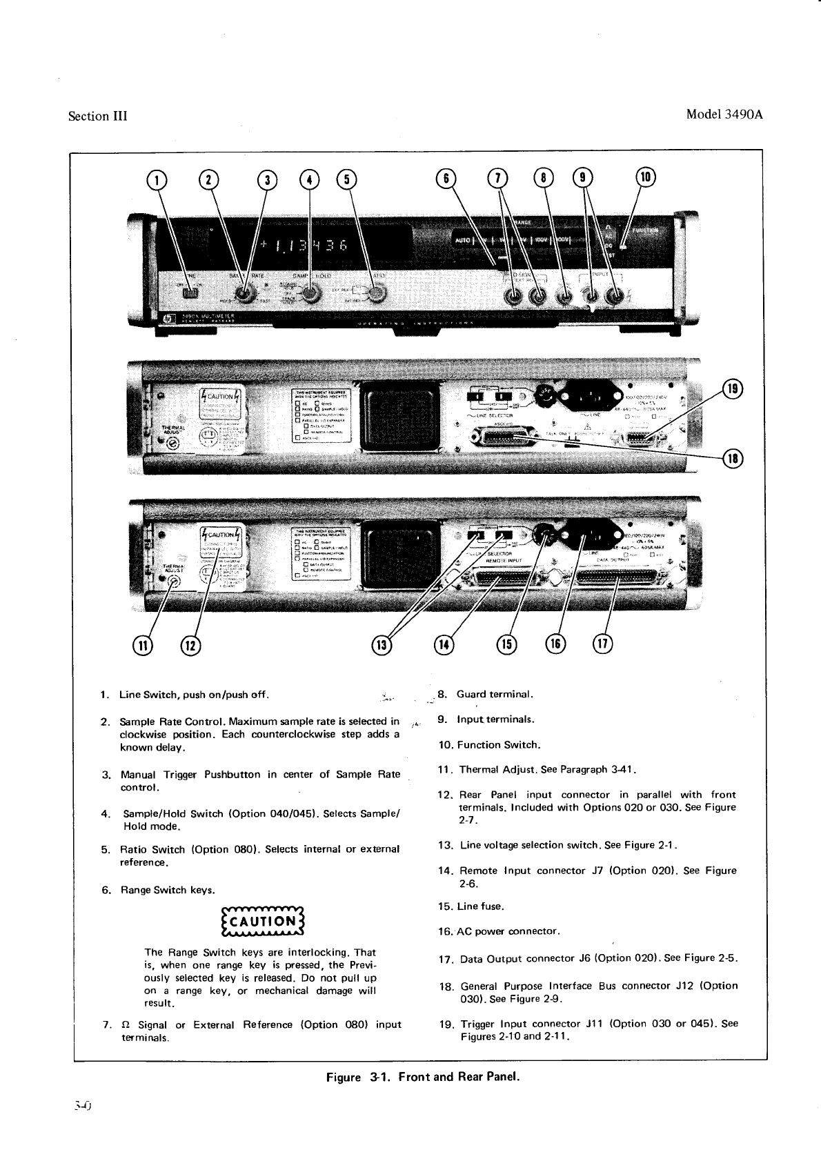
Section
III Model3490A
1.
2.
Line Switch, push on/push off. .'^".
Sample Rate Control. Maximum sample rate is selected in
clockwise position. Each counterclockwise step adds a
known delay.
Manual Trigger Pushbutton in center of Sample Rate
control.
Sample/Hold Switch (Option o4o/045). Selects Sample/
Hold mode.
Ratio Switch (Option 0801. Selects internal or external
referen@.
Range
Switch keys.
The Range
Switch keys are interlocking.
That
is, when one range key is pressed,
the Previ-
ously selected
key is released.
Do not pull up
on a range key, or mechanical damage will
result-
a Signal or External Reference (Option O80l input
terminals.
. ._.8. Guard terminal,
i\- 9. InPut
terminals.
10. Function Switch.
1
1. Thermal Adjust. See
Paragraph
3-41.
'|
2. Rear Panel input connector in parallel with front
terminals. Included
with Options 020 or 030. See
Figure
2-7.
1 3. Line voltage selection switch. gee Figure 2-1
.
14. Remote Input connector J7 (Option 0201. See Figure
2-6.
1
5. Line
fuse.
16, AC power @nnector.
17. Data Output connector
J6 (Option
0201.
See
Figure
2-5.
18. General
Purpose
Inter{ace Bus connector J12 (Option
030).
See
Figure 2-9.
19. Trigger Input connector J1 l (Option 030 or 045). See
Figures 2-l0 and2'11.
J.
4.
5.
6.
l-rJ
Figure
31. Front and
Rear Panel.
Model3490A Section
III
SECTION III
OPERATING
INSTRUCTIONS
3-1.
INTR0DUCTI0N.
3-2. This section contains instructions for using the
Model 34904 Multimeter to make dc voltage, ac voltage
and resistance
measurements.
It also includes instruc-
tions for sample/hold and ratio measurements, remote
control and data output. Basic operating instructions
may be found on a pull-out card at the bottom edge
of
the 3490A
front Panel.
3.3.
INSTBUMENT
CAPABI
LITIES.
3-4.
Standard
I nstrument.
3-5. The standard
Model 3490A Multimeter makes dc
voltage, ac voltage and resistance
measurements with
S-digit resolution
and
up to I 20
%
of range on all ranges
except l000Vac to dc. The 3490A has five dc voltage
ranges,
.l V to 1000V; 4 ac voltage ranges,
I V to
1000V; and
six resistance ranges,
I kO to 10,000kQ.
Ranging
may be manual
or automatic. Polarity
selection
and display
are
automatic.
A self-test feature is included
which checks
certain operations within the instrument.
3-6. Output
and Remote Gontrol 0ptions.
3-7. Data Output Option 021 and Remote Control
Option 022. Option 021
provides
ten columns of binary
coded decimal (BCD) output data. This data may be
either HIGH true or LOW true, as selected by a slide
switch on the outguard data output printed circuit
assembly. With Option O22, the 349OA range and
function may be programmed by LOW true input
information. External triggering is possible
with either
option.
3-8. General Purpose Interface Bus ll0 Option
030. The General Purpose
Interface Bus I/O (GPIB)
option permits
remote
programmhg
and data
output on
the same
bus lines. The 3490A may be connected
to a
bus in parallel with several other instruments and
controlled by a single
controlling instrument.
Remote
control
of range,
function,
trigger mode and sample/hold
mode is possible
with Option 030. The output data
includes
measurement
status,
function, polarity, magni-
tude and range,
in the format given
in Paragraph
3-126.
Controlling instruments that may be used with the
3490A GPIB option include the -hp- 9800A series
calculators
and the -hp- Model 3260A Marked Card
Programmer.
3-9.
Sample/Hold
0ption
040
or
045.
3-10.
The
Sample/Hold
Option
(040
or 045)
enables
the
\todel 3-190.{
Multimeter to sample
a changing input
voltage
and hold that sample
long enough to measure its
amplitude. This permits pulse
height measurements and
digitization of changing
waveforms
such
as ramps or sine
waves.
The extemal trigger circuits are
isolated
from the
signal input Low terminal and from chassis
ground,
which allows the voltmeter to make guarded
floating
measurements. The designations
used for the 34904
Sample/Hold options are as
follows:
When Sample/Hold
is
installed The
Sample/Hold
option
in a 3490A with: is designated as:
BCDiRemote
Expand
Option 020 Option 040
GPIB
Option
030 Option
040
Neither 020 or 030 Option 045
3-11. Batio
0ption
080.
3-12. The 3490A equipped with Ratio Option 080 is
capable of making three-wire dc-to-dc or ac-to-dc ratio
measurement. Two External Reference ranges are pro-
vided, the I V range accepting reference
voltages of
10.1 V to t 1.2V, and the 10V range accepting
voltages from
t I V to t 12V.
3.13.
FRONT AND
REAR
PANEL
OESCRIPTION.
3-14. Figure 3-l shows the front and rear
panel
controls
and connectors
and gives
a brief description
of each.
Some of the features shown are available onlv with
certain options.
,.
3-15.
MAXIMUM INPUT
VOLTAGES.
3-l 6. Table 3-l lists the maximum allowable voltages
between
input terminals,
and between the
terminals
and
chassis. These maximum voltages are also
shown on the
front panel and must not be exceeded or damage
to the
instrument
may
resull.
wAR]ililG
If the 34904 has a rear input connector,
the front and rear terminals are internally
connected in puallel. If high voltages may
be applied, always protect the open termi-
nals. Be ilre the rear input terminals are
open before connecting an input to the
front terminals and vice versa.
3-l
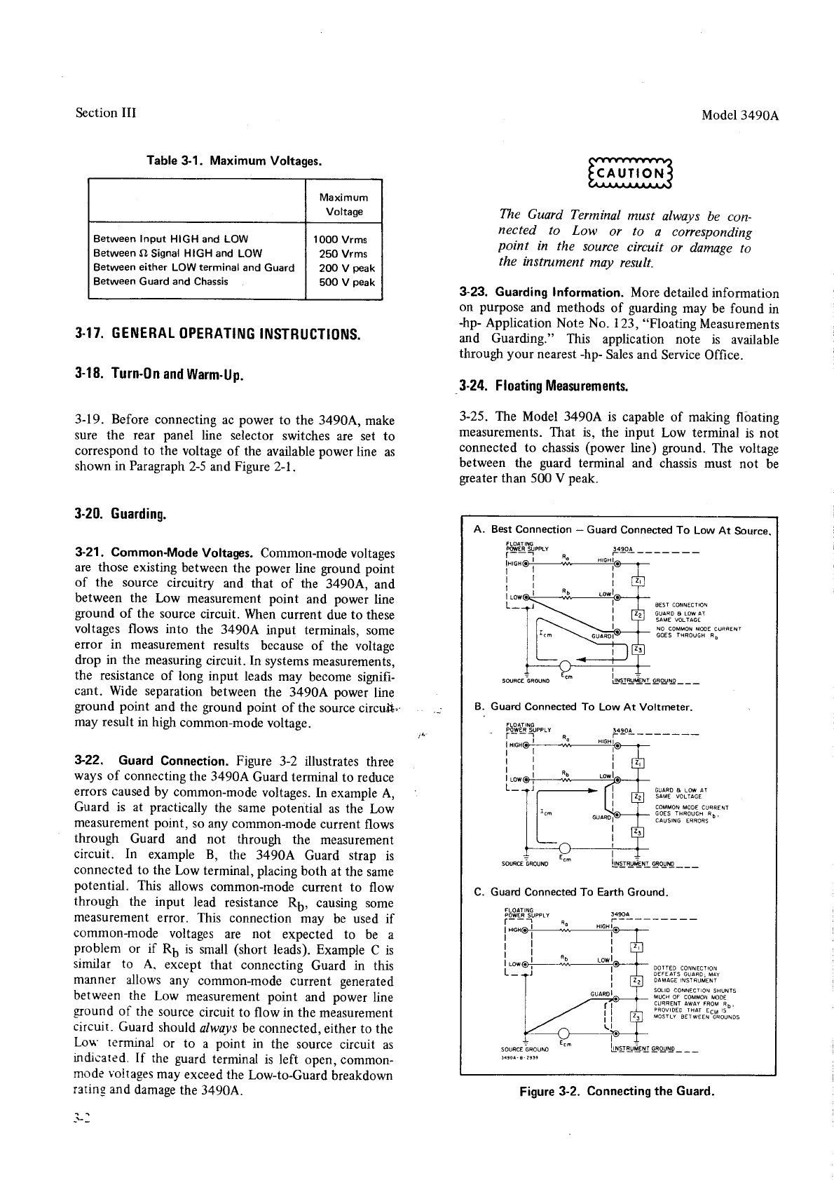
Section
III
Table
3-1 . Maximum
Voltages.
Maximum
Voltage
Between Input HIGH and LOW
Between fi Signal HIGH and LOW
Between either LOW terminal and Guard
Between Guard and Chassis
100O
Vrms
250 Vrms
2O0 V peak
500 V peak
3.I 7. GENERAL
OPERATING
INSTRUCTIONS.
3-18. Turn-On
and
Warm-Up.
3-19. Before
connecting
ac
power
to the 3490A,
make
sure the rear panel line selector switches
are set to
correspond to the voltage
of the available power
line as
shown
in Paragraph
2-5 and Figure 2-1.
3-20. Guarding.
3-21. Common-Mode
Voltages. Common-mode
voltages
are those
existing between
the power
line ground
point
of the source
circuitry and that of the 34904, and
between the Low measurement point and power line
ground of the source
circuit. When current due
to these
voltages
flows into the 3490A input terminals, some
error in measurement
results because
of the voltage
drop in the measuring
circuit. In systems
measurements,
the resistance
of long input leads
may become signifi-
cant. Wide separation
between
the 3490A power line
ground
point and
the ground
point of the source
circuiü,
may
result in high
common-mode
voltage.
3-22. Guard Connection. Figure 3-2 illustrates
three
ways
of connecting
the 3490A
Guard terminal
to reduce
errors caused
by common-mode
voltages.
In example
A,
Guard is at practically
the same
potential as the Low
measurement point, so any common-mode
current
flows
through Guard and not through the measurement
circuit. In example B, the 3490A Guard strap is
connected
to the Low terminal, placing
both at the
same
potential. This allows common-mode
current to flow
through the input lead resistance
R6, causing some
measurement
error. This connection may be used if
common-mode voltages are not expected to be a
problem or if R6 is small
(short leads). Example
C is
similar to A. except that connecting Guard in this
manner allows any common-mode
current generated
between the Low measurement point and power line
gound of the source
circuit
to flow in the
measurement
circuit- Guard
should
alwoys be connected,
either to the
Lou' terminal or to a point in the source
circuit as
rrdicated. If the guard
terminal is left open, common-
mode
voltages
may
exceed
the Low-to-Guard
breakdown
r3ring and
damage
the
34904.
Model
3490A
The Guard Terminal must always be con-
nected to Low or to a corresponding
point in the source circuit or damage to
the instrument moy result.
3-23. Guarding Information. More detailed
information
on purpose
and methods
of guarding
may be found in
-hp-
Application
Note No. 123,
"Floating
Measurements
and Guarding." This application note is available
through
your nearest
-hp-
Sales and
Service Office.
3-24. Floating Measurements.
3-25. The Model 3490A is capable
of making flöating
measurements.
That is, the input Low terminal is not
connected
to chassis
(power line) ground.
The voltage
between the guard terminal and chassis must not be
geater
than 500
V peak.
r---
A. Best
Connection - Guard Connected To Low At Source.
44904
-------- - -
EEST
CONNECITON
SAME VOLTAGE
NO COMMON MOOE
CURRENI
GOES
IHROUGH Rb
9!9!'!-9 _ _ _
B. Guard Connected To Low At Voltmeter.
sÄME VOLIACE
COMMON MOOE
CURRENT
6OES TBROüGH
Fb,
CAUSIN6 ERRORS
9E0!{q__ _
C. Guard Connected To Earth Ground.
DOITEO
CONNECIION
DEFEAIS
GIAROI MAY
OAMACE INSIqUMENT
SOLIO
CONN€CION
SHUNTS
MUCH
OF COMMON MOOE
CURRENT AWAY FROM
Rh,
PROVIDED
THAT ECM
15-
MOSILY 8€TWEEN
GROUNOS
GROUNO
FLOATING
r'-
- -l
i*.J
Figure
3-2.
Connecting the Guard.
Model
3490A
3-26.
0verrange
Measürements.
3-27. Measwements
within rated accuracy are possible
up to 120 7o
of runge
on all except the 1000
Vac or dc
ranges. Overrange
inputs on these
ranges
would exceed
the maximum allowable input voltage. The display
includes the overrange
"1" as
the sixth digit.
3-28. Overload
Indication.
3-29. lf the measurement
is 120
% of nnge or geater,
the Overload
"OL" annunciator will light. The
numerical
display will read
120000 to 120005.
3-30.
Bange
Indication.
3-31. The 349OA display always reads in volts or
kilohms (except in Ratio measurements),
with the
decimal point and range switch indicating the range
selected. In autorange mode, the decimal point alone
indicates
range.
3-32.
Function Indication.
3-33. In the standard 3490A, function is indicated only
by the function switch position. If optional Remote
control is in use, the "REM" annunciator lights to
indicate that the front panel switches
are disabled. An
available
special display assembly
adds V, AC, Kfl and
TST annunciators
to indicate the function selected.
3-34.
Autoranging.
3-35. In the autorange
mode,
upranging
occurs at l2O%
of range and downranglng
at lOVo
of range. Ameasure-
ment sequence
is not completed unless the reading
is on
the proper range. For example, if the Sample Rate
control is set to Hold and the Manual Trigger push-
button depressed
once, the 3490A will continue to
sample
until one reading
is taken
on the correct
range.
When the 3490A is changed
to the autorange
mode from
a voltage range, the first reading in autorange is not
valid.
3-36.
ManualTrigger.
3-37. Manual triggering is available
on all instruments.
When the Sample Rate control is set to Hold, one
measurement
results
each
time the Manual pushbutton is
depressed.
If the pushbutton is depressed
while the
instrument is not in the Hold condition, automatic
sampling
will stop
until the button is released.
3.38.
SELF.TEST
OPERATION.
3-39. The Intemal Test function of the 3490A verifies
proper operation of most of the dc circuits, logic
circuits,
and the ohmmeter
reference.
Use
the
following
procedure
to perform the Intemal
Tests.
If Test
No. I ii
not correct,
refer to the Troubleshootingsection.
Ifany
of the other tests
are not correct,
refei to the perfoi_
mance
Checks.
Section
III
a. Set Function to TEST. If instrument has
Ratio or
Sample/Hold options, set RATIO to INT REF and
SAMPLE/HOLD
to OFF.
b. Set SAMPLE RATE control one position clock-
wise from HOLD.
c. Select
RANGE l, which is Logic Test.
The display
should
_follow
the sequence
below, starting at any point
in the list. All readings
should be in the order ih-own,
with the polarity sign, numbers, and decimal points ai
shown. The last reading listed displays
all digiis as
the
count accumulates,
then stops at the number shown.
The,last two digits in the last number are not significant
to the test. If these
displays
are correct,
most of the
logic circuits are
operating
correctly.
+ 080.024
+
o4.oo24
+ 0.20024
+
.0too24
+
0.09032
+ to.oo24
+ 200.024
+ 4000.24
+
80002.4
+
6000.xx
OL
d. Select
RANGE
2. The
display should
be .000000
t 2 counts.
This
verifies
the
l0 V range
zero.
e. Select
RANGE 3. Difference
between
+ and -
readings
should
be
(8 counts.
f. Select
RANGE
4. Using
a dc standard
having
an
accuracy
of t 0.01
% or better, apply an input of
- 10.0000
V. Display
should
be
+
09.9990
+ (16
counts
+
dc standard
error).
This
checks
the
+ Reference.
Ifthe
3490A
has the
ratio
option,
set
RATIO to EXT REF
l0 V and short EXT REF input terminals.
Display
shoüld
be r 00.0000.
This checks the Ratio
Reference
dmplifier zero. Return RATIO switch to INT REF
position
and
remove
short
from
input.
g. Select RANGE
5. Display
should
be
000.000 t t5
'counts,
verifying
the
0.1 V range
zero.
h. Select
RANGE
6. Using
a dc standard
having
an
accuracy
of t 0.01
% or better, apply an input of
- 10.0000V.
Display
should
be
- 1000.00
I (35
counts
+
dc standard
error).
This ehecks
the dc input 0.01
attenuation
and
the dc
amplifier
xl00 gain.
i. Select
RANGE 7. Short fl SIGNAL
terminals.
Dsplay
should
be
- 09700.0 1 7000 counts.
This
verifies
proper
operation
of the
Ohms
Converter.
3-40. DC
VOLTAGE
MEASUREMENTS.
341. For optimum
accuracy
of measurements
on the
.l V range,
first
short
the
input
terminals
with
a
copper
J-J
Section
III
bar or a large solid copper wire, and adjust
AlR429
(Thermal Adj) for zero display. AlR429 is accessible
through
the rear
panel.
If the 3490A has
the rear
input
connector,
loosen the hinged cover to gain access
to
AlR429.
Be wre to connect the Guard Terminal
and to observe
the maximum voltage limi-
tations noted on the front panel and in
Table 3-1, or damage ta the instrument
may rewlt.
3-42.
DC Sample
Rate
and
Response
Time.
3-43. The sample
rate and response
time for dc voltage
measurements
are
shown in Table
3-2.
Table
3-2. Sample
Rate
and Response
Time.
*Sample Rate Control set to FAST position and instrument
not in overload. Each counterclockwise step adds 240 ms in
Option 050 instruments,
200 ms in Option 060 instruments.
3-44.
Input Resistance.
345. Input resistance
in the dc function is
greater than
101
o ohms on the .1
V, I V, and
10V ranges,
and l0
megohms
t 0.1 5
7o
on the 100
V and
1000 V ranges.
3.46.
AC VOLTAGE
MEASUREMENTS.
Be sure to connect the Guard Terminal
and to observe
the maximum voltage limL
tations noted on the front panel and in
Table 3-1, or damage to the instrument
may result, and high frequency measure-
ments will be in enor-
341 . The display
will NOT rcad
zero
on any ac range
with the input shorted.
The indication
on all
ranges
with
the input shorted should be less
than 50 counts.
The
accuracy
of ac measurements
below 1.0%
of full range is
not specified.
3-48.
AC
Sample
Rate and
Response
Time.
-3-49.
The sample rate and
response
time for ac
voltage
measurements
are shown
nTable 3-2.
Model
3490A
3-50.
Frequency
Bange.
3-51.
Frequency
range
of the ac
converter
is 20Hz to
250kHz, r"itft u maximum volt-Hertz
product of 107.
That is, the frequency
range
for the I V and
l0 V ranges
is 2OHz to 250
kHz, but the maximum frequency
at
100
V is 100 kHz,
and at 1000
V it is
l0 kHz.
3-52.
Input lmpedance.
3-53. Input impedance
in the
ac
function
is the same on
all ranges,
and is 2 MO t I %
in panllel with ( 65 pF in
instruments
without rear panel input and (90pF in
instruments
having
tire rear
panel
input connector'
3-54.
Harmonic
D istortion.
3-55. The 3490A has an average-responding
ac-dc
con-
verter circuit calibrated to display the rms value of a
sinusoidal
input. Therefore,
any
distortion
present in the
input signal will affect the accuracy of the measure-
ments as shown
in Table
3-3.
Table 3-3. Distortion
Error.
Harmonic % Distortion
Yo Error
{*Fundamental)
Max.
Positive
Max.
Negativr
Any
even
o.1
0.5
1.0
2.O
0.000
0.001
0.005
0.020
Third 0.1
o.5
1.0
2.o
o.033
0.1
68
0.338
0.687
0.003
o.167
0.328
0.667
Fifth 0.1
o.5
1.0
2.O
0.020
0.1 01
0.205
o.420
0.020
o.099
0.195
1.380
*Depends on phase
relationship between harmonic and
fundamental.
3.56.
RESISTANCE
MEASUREMENTS.
3-57. When the 3490A is making resistance
measure-
ments, movement of the instruction card will cause
display readings
to jump. For optimum accuracy
of
mtusur.*ents on the .1
kO range'
first set Range
and
Function to .1V dc, short the input terminals
with a
copper bar or large solid copper wire, and adjust
efn+zq (Thermal Adj) for zero display' A1R429 is
accessible
through the rear
panel.
If the 3490A has
the
rear input connector,
loosen
the hinged
cover
to gain
access
to the adiustment.
Function
Minimum Sample
Period* Response
Time
Option
050 Option
O60
DC
Volts
AC
Volts
Ohms
.1
k thru
100
ko
1,O00
kf,,
10,000
ko
240.2ms+5ms
1.26s+.025s
240.2ms+5ms
300.2ms+6ms
660.3
ms
+ 12 ms
200.1
ms+4ms
1.05s+.025s
200.1
ms+4ms
250.1
ms+5ms
550.2
ms
+ l0 ms
200.1
ms
1.05 s
2OO.1
ms
25O.1
ms
550.2
ms
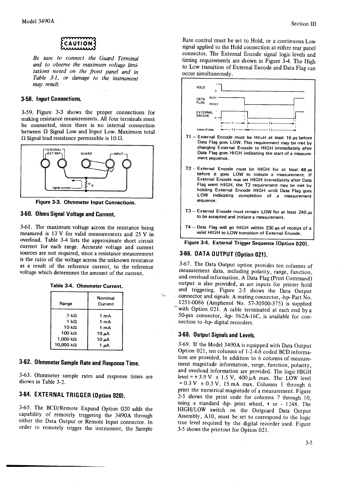
Model3490A
Be sure to connect the Guord Terminal
and to obserye
the maximum voltage limi-
tations noted on the front panel and in
Table 3-1
, or damage to the instrument
may result.
3-58.
Input Connections
3-59. Figure 3-3 shows the proper connections
for
making resistance
measurements.
All four terminals
must
be connected, since there is no internal connection
between O Signal
Low and Input Low. Maximum total
O Signal
lead resistance
permissible
is 10 O.
O SIGNAL
Section
III
Rate
control
must be set
to Hold, or a continuous
Low
signal
applied to the Hold connection
at either
rear panel
connector.
The External Encode
signal
logic levels
and
timing requirements
are shown in Figure 34. The High
to Low transition
of External
Encode
and Data
Flae
can
occur
simultaneously.
HOLD
Pilä:::",----__1_ r
EXTERNAL
,
ENCODE
o
34904.81&
Tl - External Encode must be HtLiH at teast 16 ps before
Data Flag goes LOW. This requirement rnay be met by
changing External Encode to HIGH immediately after
Data Flag goes HIGH indicating the start of a measure-
ment sequenoe.
T2-External Encode müSt be HIGH for at least 4gps
before it goes Low to initiate a measurement. lf
External Enmde was set HtGH immediately after Data
Flag went HIGH, the T2 requirement rnay be met by
holding External Encode HIGH until Data Flag goes
LOW indicating completion of a measurement
sequence.
T3 - External Encode must rernain LOW for at least 24O
ps
to be accepted
and initiate a rEasurement.
T4 - Data Flag will go HIGH within 230 ps of receipt of a
valid HIGH to LOW transition of External Enc,ode.
Figure
3-3. Ohmmeter lnput Connections.
3-60. 0hms Signal
Voltage
and
Current.
3-61. The maximum voltage across the resistance
being
measured
is 13
V for valid measurements
and 25 V in
overload. Table 3-4 lists the approdmate short circuit
current for each range. Accurate voltage and current
sources
are not required,
since
a resistance
measurement
is the ratio of the voltage
across
the unknown resistance
as a result of the reference current, to the reference
voltage
which determines
the amount of the currenr.
Table
34. Ohmmeter
Current.
Range
Nominal
Current
.l ko
lko
10
ko
100
ko
1,000
ko
10,000
ka
1mA
lmA
lmA
10
pA
10
pA
1 ttA
3-62.
0hmmeter
Sampte
Rate
and
Besponse Time.
3_-63.
Ohmmeter sample
rates and response
times are
shown
in Table
3-2.
3-64.
EXTERNAL
TRtcGER
(Option
020).
365. The BCD/Remote
Expand Option 020 adds
the
capability of remotely rriggering
the 3490A through
either the Data Output or Remote
Input connector.
In
order to remotely trigger the instrument, the Sample
Figure
3-4. External
Trigger
Sequence
(Option
020).
3-66.
DATA
0UTPUT
(Option
021).
3-67. The
Data
Output option provides
ten columns
of
measurement
data, including
polarity, range,
function,
and
overload
information.
A Data
Flag (prini Commandj
output is also provided,
as
are inputs for printer hold
and triggering. Figure 2-5 shows the Data Output
. connector
and
signals.
A mating
connector,
-hp part No.
. 1251-0086
(Amphenol
No. 57-30500-375)
is supptied
" with Option 021
. A cable
terminated
at each .nä'by u
50-pin connector,
-hp- 562A-16C,
is available
for con-
nection
to -hp-
digital
recorders.
3-68.
Output
Signals
and Levels.
3-69. If the
Model
3490{is equipped
with Data
Output
Option 02l ,Ien columns
of l-24-8 coded
BCD
informa-
tion are
provided,
In addition to 6 columns
of measure-
ment magnitude
information, range,
function, polarity,
and
overload
information are
provided.
The logic
HIGH
level
=
+
3.9
V r 1.5
V, 400
pA max. The LOW level
=0.3V + 0.3V, l5mA max.
Columns
I through
6
print the numerical
magnitude
of a
measurement.
Figure
2-5 shows
the print code for columns 7 through 10,
using a standard
-hp- print wheel, + or - 124g. The
HIGH/LOW switch on the Outguard Data Output
Assembly,
Al0, must
be
set
to correspond
to the logic
true level
required
by the digital recorder
used.
Figure
3-5
shows
the printout for Option
021.
3-5
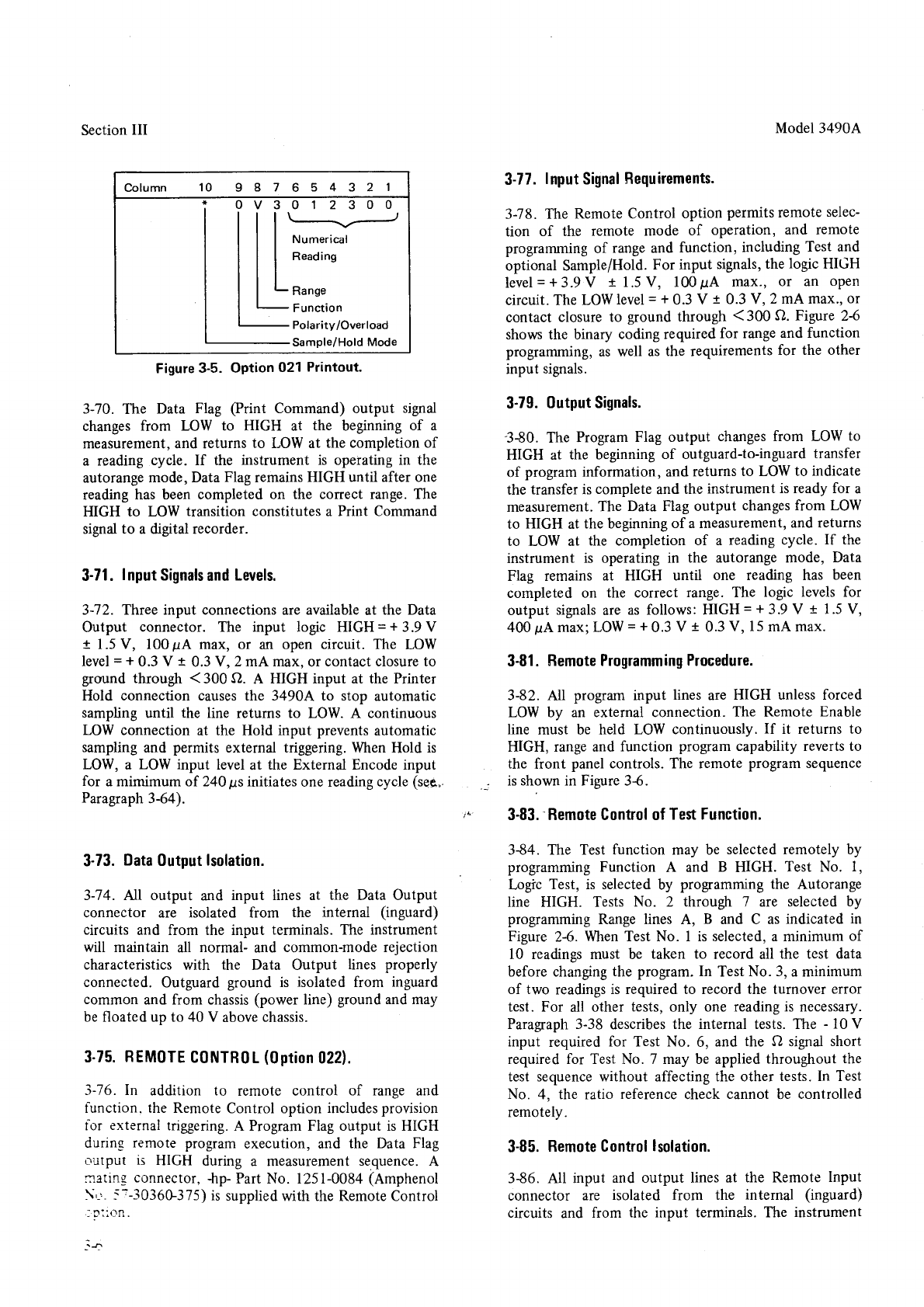
Section
III
3-70. The Data Flag @rint Command) output signal
changes
from LOW to HIGH at the beginning
of a
measurement, and returns
to LOW at the completion of
a reading
cycle. If the instrument is operating
in the
autorange
mode, Data
Flag
remains
HIGH until after one
reading
has been completed on the correct range. The
HIGH to LOW transition constitutes a Print Command
signal to a digital recorder.
3-71.
Input
Signals
and
Levels.
3-12. Three input connections
are
available
at the Data
Output connector. The input logic HIGH = + 3.9 V
+ 1.5V, l00pA max, or an open circuit. The LOW
level
= + 0.3 V t 0.3 V. 2 mA max.
or contact closure to
ground through < 300 A. A HIGH input at the Printer
Hold connection causes the 3490A to stop automatic
sampling
until the line returns to LOW. A continuous
LOW connection
at the Hold input prevents
automatic
sampling
and permits
external triggering. When
Hold is
LOW, a LOW input level
at the External Encode input
for a mimimum of 240
ps
initiates
one reading
cycle
(see.
Paragraph
3-64).
3-73.
Data
0utput
lsolation.
3-74. Nl output and input lines at the Data Output
connector are isolated from the internal (inguard)
circuits and from the input terminals. The instrument
will maintain all normal-
and common-mode rejection
characteristics
with the Data Output lines properly
connected.
Outguard
ground is isolated from inguard
common
and from chassis
(power
line) ground
and may
be floated up to 40 V above
chassis.
3-75.
REMOTE
C0NTROL
(0ption
022).
3-76. In addition to remote control of range
and
iunction. the Remote
Control option includes provision
for external
triggering.
A Program Flag output is HIGH
during remote program
execution, and the Data Flag
rrulput is HIGH during a measurement
se,quence.
A
:natinE
connector.
*rp- Part No. 125 l-0084
(Amphenol
\-' r:-3036G375)
is suppliedwith
the Remote Control
.t
ol:on.
la
Model34904
3-77.
Input
Signal
Requirements.
3-78. The Remote
Control option permits
remote
selec-
tion of the remote mode of operation, and remote
programming of range and function, including
Test and
optional Sample/Hold.
For input signals,
the
logic
HIGH
level
= +
3.9 V r 1.5
V, 100
pA max., or an open
circuit. The LOW
level
= + 0.3
V t 0.3 V, 2 mA max.,
or
contact
closure to ground
through <300 O. Figure 26
shows the binary
coding required
for range
and function
programming,
as well as
the requirements
for the other
input signals.
3-79.
0utput Signals.
-3-80.
The Program
Flag output changes from LOW to
HIGH at the beginning
of outguard-to-inguard
transfer
of program information, and
returns
to LOW to indicate
the
transfer is
complete
and
the
instrument
is ready for a
measurement.
The Data Flag output changes from LOW
to HIGH at the beginning
of a measurement,
and returns
to LOW at the completion of a reading cycle. If the
instrument is operating in the autorange mode, Data
Flag remains at HIGH until one reading has been
completed on the correct range. The logic levels for
output signals
are as follows: HIGH = + 3.9 V t 1.5 V,
400
l,rA
max; LOW
=
+
0.3
V r 0.3
V, l5 mA max.
3-81. Remote Programming
Procedure.
3-82. All program
input lines are HIGH unless forced
LOW by an external connection.
The Remote Enable
line must be held LOW continuously.
If it returns to
HIGH, range and
function program
capability reverts to
the front panel
controls. The remote
program
sequence
is shown in Figure 3-6.
3-83.'Remote Gontrol 0f
Test Function.
3{4. The Test function may be selected remotely by
programming Function A and B HIGH. Test No. 1,
Logic Test, is selected
by programming the Autorange
line HIGH. Tests No. 2 through 7 are selected
by
programming
Range lines A, B and C as
indicated
in
Figure 2-6. When Test No. I is selected, a minimum of
l0 readings must be taken to record all the test data
before changing
the program. In Test No. 3,
a minimum
of two readings
is required to record the turnover
error
test. For all other tests,
only one reading
is necessary.
Paragaph 3-38 describes
the internal tests. The - 10 V
input required
for Test No. 6, and the Q signal
short
required for Test No. 7 may be applied
throughout
the
test sequence without affecting the other tests. In Test
No. 4, the ratio reference
check
cannot be controlled
remotely.
3-85.
Remote Control
lsolation.
336. All input and output lines at the Remote Input
connector are isolated from the internal (inguard)
circuits and from the input termina-ls. The instrument
Column 10
-_-_ll-
947654321
0v3012300
l+
I Numerical
I Readino
L *"nn"
F unction
Polarity/Overload
Sample/Hold
Mode
Figure
3-5. Option
021
Printout.
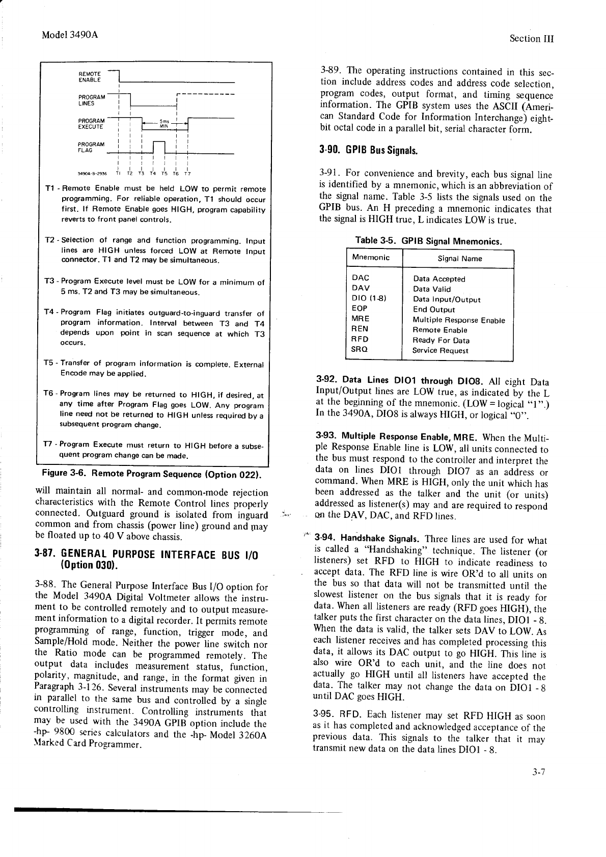
REIUOTE
ENAELE
PROGRAI\,I
LINES
PROGRAM
EXECUTE
PROGRAM
349A.4-2936
lttltl
rtllll
lrrttll
II T2 T3 T4 15 T6 T7
Tl - Remote Enable must be held LOW to permit remote
programming. For reliable
operation,
T1 should occur
first. lf Remote Enable
goes
HIGH, program
capability
reverts to front panel controls.
T2 -
Selection of range and f
unction programming. Input
lines are HIGH unless forced LOW at Remote lnput
connector. T1 and T2 may be simultaneous.
T3 -
Program
Execute level
must be LOW for a minimum of
5 ms. T2 and
T3 may
be simultaneous.
T4 - Program Flag initiates ourguard-to-inguard transfer of
program information, Interval between T3 and T4
depends upon point in scan sequence
at which T3
occurs.
T5 - Transfer of program information is complete. Exrernar
Encode may be applied.
T6 -
Program
lines may be returned
to HIGH, if desired,
at
any time after Program Flag goes LOW. Any program
line need
not be returned
to HIGH unless
required
by a
subsequent
program change.
T7 -Program Execute must return to HIGH before
a subse-
quent program change
can be made.
Model
34904 Section
III
3-89. The operating
instructions
contained
in this sec-
tion include address
codes
and address
code selection,
program codes, output format, and timing sequence
information. The GPIB system
uses
the ASCII (Ameri-
can Standard
Code for Information Interchange)
eight-
bit octal
code
in a
parallel
bit, serial
character
form.
3-90.
GPIB
BusSignals.
3-91. For convenience
and brevity,
each
bus signal
line
is identified
by a mnemonic,
which is
an abbreviation
of
the signal
name.
Table 3-5 lists the signals
used
on the
GPIB bus.
An H preceding
a mnemonic
indicates
that
the
signal
is HIGH true,
L indicates
LOW is
true.
Table
3-5. GPIB
Signal
Mnemonics.
Mnemonic Signal Name
DAC
DAV
Dro
(1€)
EOP
MRE
REN
RFD
sRo
Data Accepred
Data
Valid
Data
lnput/Output
End
Output
Multiple
Response
Enable
Remote
Enable
Ready For Data
Service Request
Figure
3-6. Remote
Program
Sequence
(Option
022).
will maintain all normal- and common.mode
rejection
characteristics
with the Remote
Control lines properly
connected.
Outguard ground is isolated
from inguard
common
and
from chassis
(power
line) ground
and r-nay
be
floated
up to 40 V above
chassis.
3-87.
GENERAL
PURPOSE
INTERFACE
BUS I/O
(0ption
030).
3.-88
_The
General
Purpose
Interface
Bus
I/O option for
the Model 3490A Digital Voltmeter allows the instru_
ment to be controlled
remotely
and to output measure_
ment
information
to a digital
recorder.
It peimits
remote
programming of range, function, trigger mode, and
Sample/Hold
mode. Neither the poweiline switch
nor
the Ratio mode can be programmed
remotely. The
output data includes measurement
status, function,
polarity, magnitude,
and range,
in the forrnat given
in
Paragaph
3-126.
Several
instiuments
may be connected
in parallel
to the same
bus and controlied by a sinsle
controlling insrrumenr.
Controlling
instruments
thlat
may be used
with the 34904 GpIB option include
the
-hp 9800 series
calculators
and the _hp_
Model 32604
\larked
Card
Progammer.
3-92.
Data Lines
DlOl through
DlOg. All eight
Data
Input/Output lines
are
LOW true, as indicated
by the L
at the beginning
of the
mnemonic. (LOW
=
logical
..1".)
In the
3490A,
DIO8
is
always
HIGH,
or
logical
..0".
3-93.
Multiple
Response
Enable,
MRE. When
the
Multi_
ple Response
Enable
line is LOW,
all units
connected
to
the bus
must respond
to the
controller
and interpret
the
data on lines DIOI through DIOT as an adäress
or
command.
When
MRE is HIGH, only the unit which
has
been
addressed
as the talker
and the unit (or units)
addressed
as listener(s)
may and
are
required
to respond
0n the
DAV, DAC,
and
RFD lines.
'"' 3-94. Handshake
Signals.
Three
lines
are used
for what
is called a "Handshaking"
technique.
The listener
(or
listeners)
set RFD to HIGH to indicate readiness
to
accept
data.
The RFD line is wire OR'd to all units on
the bus so that data will not be transmitted
until the
slowest
listener on the bus signals
that it is ready for
data.
When
all listeners
are
ready
(RFD goes
HIGH), the
talker
puts
the
first character
on the dattlines, DIOI _
g.
When
the data
is valid,
the talker
sets
DAV to LOW.
As
each
listener
receives
and
has
completed
processing
this
data,
it allows
its DAC output to go HIGH. This line is
also wire OR'd to each unit, and the line does not
actually go HIGH until all listeners
have
accepted
the
data.
The talker may not change
the data
on DIOI _
g
untilDAC
goes
HIGH.
3-95. RFD. Each
listener
may set
RFD HIGH as
soon
as it has completed
and
acknowledged
acceptance
of the
previous
data. This signals
to the talker that it mav
transmit
new
data
on
the
data lines
DIOI -
g.
3-1
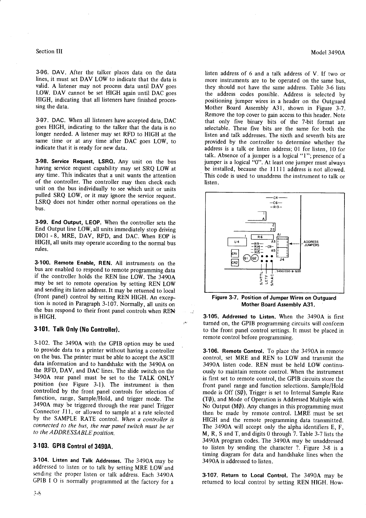
Section
III
3-96. DAV. After the talker places
data on the data
lines,
it must set DAV LOW to indicate
that the data
is
vatid. A listener
may not process
data until DAV goes
LOW. DAV cannot be set HIGItr again until DAC goes
HIGH, indicating that all listeners
have finished proces-
sing
the data.
3-97. DAC. When
all listeners
have
accepted
data, DAC
goes
HIGH, indicating to the talker
that the data is no
longer needed. A listener
may set
RFD to HIGH at the
same time or at any time after DAC goes
LOW, to
indicate
that it is
ready for new
data.
3-98. Service Request,
LSRO. Any unit on the bus
having service
request capability may set SRQ LOW at
any time. This indicates
that a unit wants
the attention
of the controller. The controller may then check each
unit on the bus individually to see
which unit or units
pulled SRQ LOW, or it may ignore the service
request.
LSRQ does not hinder other normal
operations
on the
bus.
3-99. End Output, LEOP. When
the controller
sets
the
End Output line LOW, all units immediately stop driving
DIOI - 8, MRE, DAV, RFD, and DAC. When
EOp is
HIGH, all
units
may operate
according
to the normal
bus
rules.
3-100. Remote Enable,
REN. All instruments
on the
bus
are enabled
to respond to remote
programming
data
if the controller holds the REN line LOW. The 3490A
may be set to remote operation
by setting
REN LOW
and
sending
its listen
address.
It may
be returned
to local
(front panel) control by setting
REN HIGH. An excep-
tion is noted in Paragraph
3-107.
Normally,
all units
on
the bus respond
to their front panel
controls when REN
is HIGH.
3-101. Talk
0nly
(No
Controller).
3-102. The 3490A with the GPIB option may be
used
to provide
data to a printer without having
a controller
on the bus.
The printer
must be able to accept
the ASCII
data information and
to handshake
with the 3490A on
the RFD, DAV, and DAC lines.
The slide
switch
on the
3490^ rear panel must be set to the TALK ONLY
position (see Figure 3-1). The instrument is then
controlled by the front panel
controls
for selection
of
function, range,
Sample/Hold,
and trigger mode. The
349OA may be triggered
through the rear panel Trigger
Connector
Jll, or allowed
to sample
at a rate selected
by the SAMPLE RATE control. When
a controller is
connected
to the bus,
the rear
panel
switch
must be
set
to the ADDRESSABLE position.
3-103.
GPIB
Control
of
3490A.
3104. Listen
and
Talk Addresses. The
34904 may
be
addressed
to listen
or to talk by setting
MRE LOW and
sendine
the proper
listen
or talk address. Each
34904
GPIB I O is normally programmed
at the factory for a
_r,ö
Model3490A
listen address
of 6 and a talk address of V. If two or
more instruments
are to be operated on the same
bus,
they should
not have the same
address. Table 3-6
lists
the address
codes possible.
Address is selected
by
positioning
jumper wires in a header on the Outgrrald
Mother Board Assembly A3
1, shown in Figure 3-7.
Remove
the top cover
to gain
access
to this
header.
Note
that only five binary bits of the 7-bit format are
selectable.
These
five bits are the same for both the
listen
and
talk addresses.
The sixth and seventh
bits are
provided by the controller to determine whether the
address
is a talk or listen address;01
for listen.
l0 for
talk.
Absence
of a
jumper
is a logical
"1";presence
of a
jumper is a logical
"0". At least
one
jumper
must
always
be installed,
because
the 11 1
I 1 address is not allowed.
This code
is used to unaddress the instrument
to talk or
listen.
.-al
--] | R6 lr
I u4 I -^ a3ll
rÄi+: -cg-
lL
- Rlz- aeli
l^^. | - Rrs- -- li
F-
IF<
J>
Figure
3-7. Position
of Jumper Wires
on Outguard
Mother
Board
Assembly A31.
3-105. Addressed
to Listen.
When the 3490A is first
turned on, the GPIB
programming
circuits
will conform
to the front panel
control settings. It must be placed
in
remote control
before
programming.
3-106. Remote Control. To place
the 3490A in remote
control, set MRE and REN to LOW and transmit the
3490A listen code. REN must be held LOW continu-
ously
to maintain
remote control. When the instrument
is first set to remote control, the
GPIB circuits store
the
front panel
range and function selections.
Sample/Hold
mode
is Off (S0),
Trigger is set to Internal
Sample Rate
(TQ),
and Mode
of Operation is Addressed
Multiple
with
No Output
(M0). AnV chalges in this
programming
must
then be made by remote control. LMRE must be set
HIGH and the remote programming
data transmitted.
The 3490A will accept only the alpha
identifiers
E, F,
M, R, S and T, and digits 0 through
7. Table 3-7
lists the
3490A program codes.
The 3490A may be unaddressed
to listen by sending
the character
?. Figure 3-8 is a
timing diagram for data and handshake lines
when the
3490A
is addressed
to listen.
3-107. Return to Local Control. The 3490A may be
returned to local control by setting
REN HIGH. How-
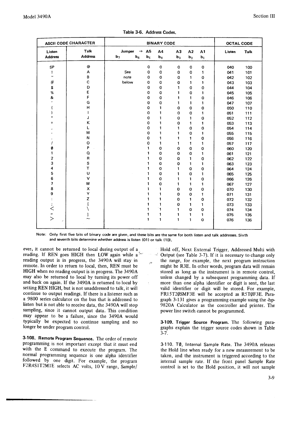
Table 3-6. Address
Codes.
ASCII
CODE
CHARACTER BINARY CODE OCTAL CODE
Listen
Address
Talk
Address
Jumper -+ A5 A4 A3 A2 A1
b7 b5 b5 b4 b3 b2 b1
Listen Talk
SP
:,
#
$
7o
1
(
l
I
0
1
2
3
4
5
6
7
8
I
;
(g'
A
I
D
E
F
G
H
I
J
K
L
M
N
o
P
o
R
S
T
U
W
X
z
t
I
00000
0000'l
00010
00011
00100
00101
00110
00111
01000
0100'l
01010
01011
01100
01101
01110
01111
10000
1000'l
10010
10011
10t00
10101
10110
10111
11000
11001
11010
11011
11100
11111
11110
See
note
below
040 100
M1 101
o42 102
043 103
o44 104
045 105
046 106
u7 'to7
050 110
o51 111
o52 't12
o53 1 13
054 114
055 115
056 116
057 117
060 120
061 121
62 122
063 123
064 124
065 125
066 126
067 '127
o70 130
o71 131
o72 132
073 133
o74 134
o75 135
076 136
Model3490A
Note: Only first five bits of binary code are
given,
and these
bits are
the same for both listen and talk addresses.
Sixth
and seventh
bits determine whether address
is listen (011
or talk (1O).
ever,
it cannot be returned to local during output of a
reading.
If REN goes
HIGH then LOW again while a
r''
reading output is in progress,
the 3490A will stay in
remote. In order
to return to local, then, REN must be
HIGH when no reading
output is
in progress.
The 3490A
may also be returned to local by turning its power off
and
back on again.
If the 3490A is returned
to local
by
setting
REN HIGH, but is not unaddressed
to talk, it will
continue
to output readings. If there
is a listener
such
as
a 9800 series
calculator
on the bus that is addressed
to
listen
but is
not able to receive
data,
the 3490Awill stop
sampling, since it cannot output data. This condition
may appear to be a failure, since the 3490A would
typically be expected to continue sampling and no
longer
be
under
program
control.
3-108.
Remote
Program
Sequence. The order
ofremote
programming
is not important except that it must end
with the E command to execute the program. The
191-ul programming
sequence
is one alpha identifier
followed by one digrt. For example, the progam
F2R4S1T2MlE
selects
AC volts,
l0V range,
Sample/
Section III
Hold off, Next External Trigger,
Addressed Multi with
'j Output (see
Table 3-7).lf it is necessary
to change
only
might be R3E. In other words,
program
data
will remain
stored as long as the instrument is in remote control,
unless
changed
by a subsequent programming
data.
if
more than one alpha identifier or digit is sent, the last
valid identifier or digit will be stored. For example,
FRl5T20SMF3E will be accepted
as R5T@F3E. Para-
graph
3-l3l gives
a programming
example
using
the
-hp-
9820A Calculator as the controller and printer. The
power
line switch cannot
be
programmed.
$109. Trigger Source Program. The following para-
graphs
explain the trigger source codes shown in Table
3_7.
3-110.
T0, Internal
Sample Rate.
The 3490A releases
the Hold line when ready for a new measurement
to be
taken, and the instrument
is triggered according to the
internal sample
rate. If the front panel Sample
Rate
control is set to the Hold position, it will not sample
3-9
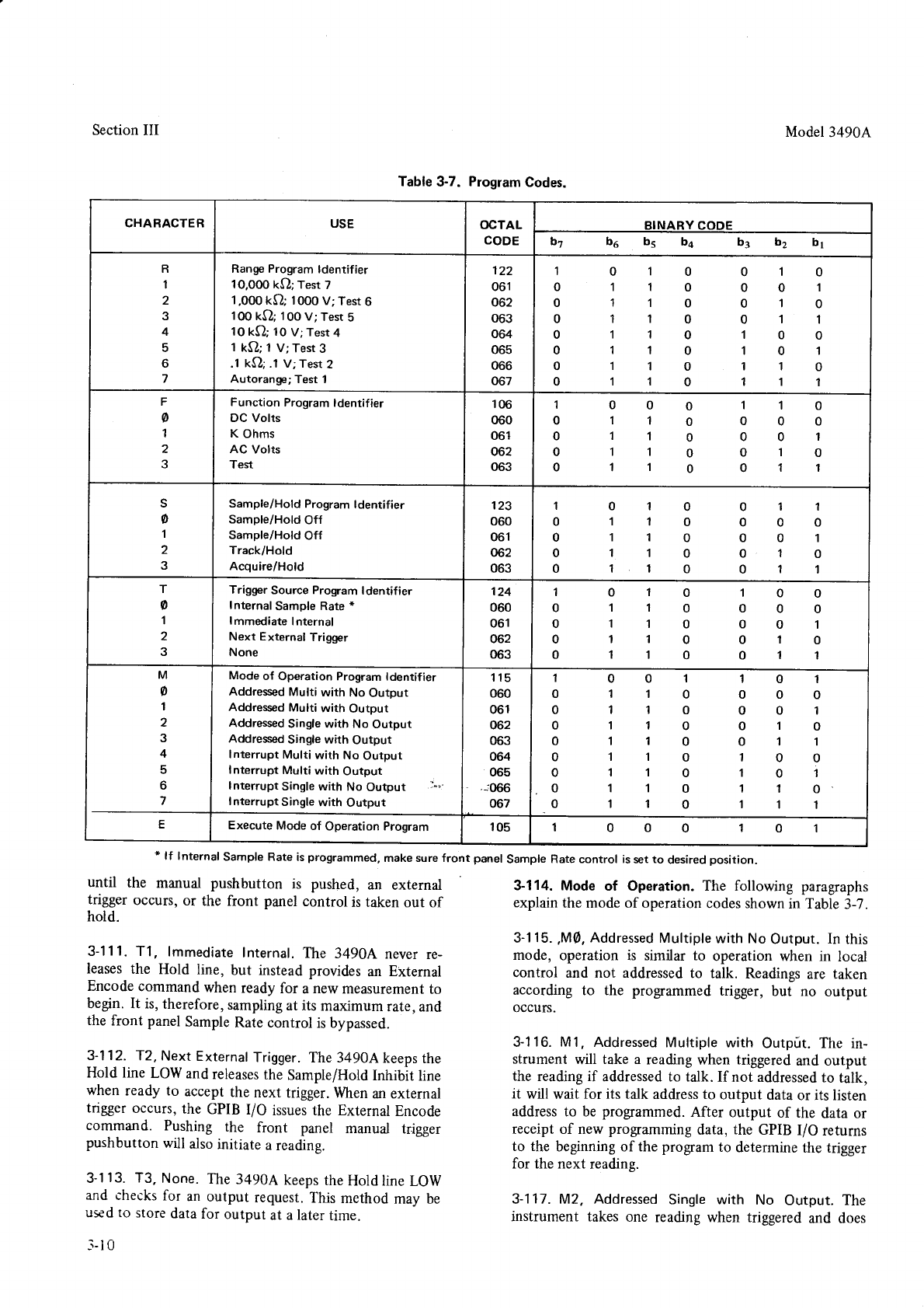
Section
III Model
34904
Table
3-7. Program
Codes.
CHARACTER USE OCTAL
CODE BINARY CODE
b1 b6 b5 ba b3 b2 b1
R
1
2
3
4
5
6
7
Range Program
ldentifier
10,00O
kf); Test
7
1
,000
kQ; l OOO V; Test
6
100
kO; 1OO
V;
Test
5
1
0 kQ; 10
V;
Test
4
1 kS2;
1 V; Test
3
.1 kO; .t V; Test
2
Autorange;
Test 1
122
061
062
063
og
065
066
067
1010010
011000'l
0110010
0110011
0110100
0110101
0110110
0110111
F
0
a
2
3
Function
Program
ldentifier
DC Volts
K Ohms
AC Volts
Test
106
060
061
62
063
1
0
0
0
0
0
1
1
1
1
0
0
0
0
0
1
0
0
o
0
1
0
0
1
1
0
0
1
0
1
s
0
1
2
3
Sample/Hold Program ldentifier
Sample/Hold Off
Sample/Hold Off
Track/Hold
Acquire/Hold
123
060
061
62
063
1
0
0
0
0
o
1
,|
1
I
1
1
1
1
1
0
o
0
0
0
0
0
0
0
0
I
0
1
a
0
1
0
1
T
o
1
2
3
Trigger Source Program
ldentifier
Internal Samole Rate *
lmmediate
Internal
Next External Trigger
None
124
060
061
062
063
1010100
0110000
0lto001
0110010
o110011
M
0
I
2
3
4
5
6
7
Mode of Operation Program ldentifier
Addressed
Multi with No Output
Addressed
Multi with Output
Addressed
Single with No Output
Addresed Single with Output
lnterrupt Multi with No Output
Interrupt Multi with Output
Interrupt Single with No Output .'-'
Interrupt
Single
with Output
115
o60
061
062
063
0il
065
.i066
067
I
0
0
0
0
0
0
0
o
0
1
1
1
1
1
1
1
1
0
1
1
1
1
1
1
1
1
1
0
o
0
0
o
0
0
0
1
0
0
o
0
1
1
1
1
0
0
0
I
1
0
0
I
1
I
o
1
0
1
0
a
o
I
EExecute Mode of Operation Program 105 10 0 00I
* lf Internal Sample Rate is
programmed, make sure front panel Sample Rate control is
set
to desired
position.
until the manual pushbutton is pushed, an external
trigger
occurs,
or the front panel
control
is taken
out of
hold.
3-1
11. T1, lmmediate
Internal.
The 3490A
never
re-
leases
the Hold line, but instead
provides
an External
Encode
command
when
ready
for a
new
measurement
to
begin. It is,
therefore,
sampling
at its
madmum rate, and
the front panel
Sample
Rate control
is bypassed.
3-112.
T2,
Next
External
Trigger.
The 3490A
keeps
the
Hold line LOW
and
releases
the Sample/Hold
Inhibit line
when
ready to accept
the
next trigger. When
an external
tngger
occurs,
the GPIB I/O issues the External
Encode
command. Pushing the front panel manual trigger
pushbutton
will also
initiate
a
reading.
3-113.
T3,
None.
The
3490A
keeps
the
Holdline
LOW
and checks
for an output request.
This
method
may be
used
to store
data
for output at a later
time.
_i-l0
3-1
14. Mode of Operation. The following paragraphs
explain
the
mode of operation
codes shown
in Table
3-7.
3-115.
.M0,
Addressed
Multiple
with No
Output.
In
this
mode, operation is similar to operation when in local
control and not addressed
to talk. Readings
are taken
according
to the programmed
trigger,
but no output
occurs.
3-116.
M1, Addressed
Multiple with Outpüt. The in-
strument
will take a reading
when triggered
and output
the reading if addressed to talk. Ifnot addressed
to talk,
it will wait for its talk address to output data
or its listen
address to be programmed.
After output of the data or
receipt of new
programming
data,
the GPIB
I/O returns
to the beginning of the program
to determine
the trigger
for the next reading.
3-117. M2, Addressed
Single with No Output. The
instrument takes
one reading when triggered
and does
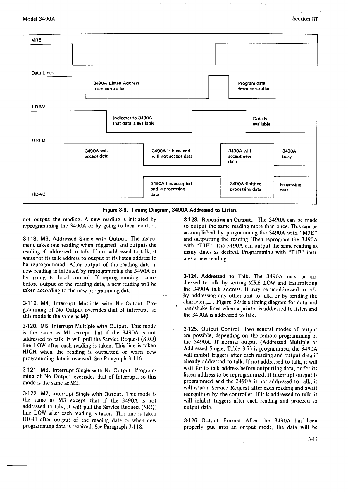
Model
3490A
not output the reading. A new reading
is initiated by
reprogramming
the 34904 or by going to local control.
3-1
18. M3, Addressed
Single
with Output. The instru-
ment takes one reading when triggered and outputs
the
reading
if addressed to talk. If not addressed
to talk, it
waits for its talk addres to output or its listen addres to
be reprogrammed.
After output of the reading data, a
new reading is initiated
by reprogramming the 34904 or
by going to local control. If reprogramming occurs
before output of the reading daIa, a new reading
will be
taken according to the new programming
data.
3-119.
M4, lnterrupt Multiple with No Output.
Pro-
gramming of No Output overrides
that of Interrupt, so
this mode is the same
as
M0.
3-120.
M5. Interrupt
Multiple with Output. This mode
is the same as Ml except that if the 3490A is not
addressed to talk, it will pull the Service
Request
(SRQ)
line LOW after each
reading
is taken. This line is taken
HIGH when the reading is outputted or when new
progamming
data
is
received.
See
Paragraph 3-l 16.
3-1
21. M6, Interrupt
Single with No Output. Program-
ming of No Output overrides that of Interrupt, so this
mode is
the same
as M2_
3-122.
MT,lnterrupt Single with Output. This mode is
the same as M3 except that if the 3490A is not
add;essed
to talk, it will pull the Service Request
(SRQ)
line LOW after each
reading
is taken.
This line is taken
HIGH after output of the reading
data or when new
programming
data is
received.
See
Paragraph 3-l 18.
Section
III
3-123. Repeating
an Output. The 3490A can be made
to output the same
reading more than
once. This
can
be
accomplished
by programming
the 3490A with "M3E"
and outputting the reading. Then reprogram
the 3490A
with "T3E". The 3490A can output the same reading
as
many times
as desired.
Programming
with "TlE" initi-
ates a
new
reading.
3-124. Addressed
to Talk. The 3490A may be ad-
dressed
to talk by setting
MRE LOW and transmitting
the 34904 talk address.
It may be unaddressed
to talk
.-by addressing
any other unit to talk, or by sending
the
character- . Figure
3-9 is a
timing
diagram
for data and
handshak'e
lines when a printer is addressed to listen and
the
3490A is
addressed
to talk.
3-125. Output Control. Two general
modes of output
are possible,
depending on the remote programming of
the 3490A. If normal output (Addressed
Multiple or
Addressed
Single, Table 3-7) is programmed,
the 3490A
will inhibit triggers
after each
reading and output data if
already addressed to talk. Ifnot addressed to talk, it will
wait for its talk address before outputting data, or for its
listen
address to be reprogrammed. If Interrupt output is
programmed
and the 34904 is not addressed to talk, it
will issue
a Service Request
after each
reading and await
recogrition
by the controller. If it is
addressed to talk,
it
will inhibit triggers after each reading and proceed to
output data.
3-1
26. Output Format.
After the 3490A has been
properly put into an ontput mode, the data will be
MRE
Data Lines
Program
data
from controller
LDAV
lndicates
to 34904
that data is available
HRFD
349OA will
accept data 349OA
is busy
and
will not accept
data 34904 will
aocept new
data
3490A finished
processing data
3490A
busy
349OA has accepted
and is
processing
data
Figure
3-8. Timing
Diagram,3490A
Addressed to Listen.
3-l I
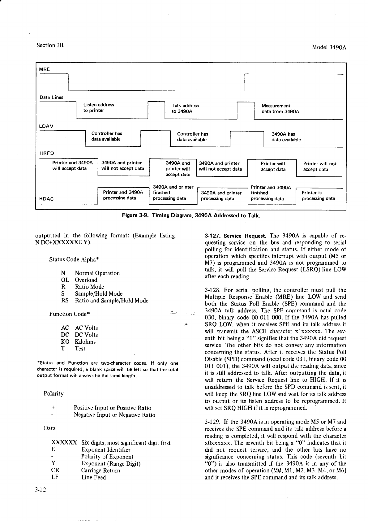
Section
III
outputted in the following format: (Example listing:
NDCfXXXXXXE-Y).
Status
Code Alpha*
N Normal
Operation
OL Overload
R Ratio Mode
S Sample/Hold Mode
RS Ratio
and Sample/Hold Mode
Function
Code*
AC AC Volts
DC DC Volts
KO Kilohms
T Test
*Status and Function are two-character codes. lf only one
character is required, a blank space will be left so that the total
output format will always
be the same
length.
Polarity
+ Positive
Input or Positive
Ratio
- Negative
Input or Negative
Ratio
Model
3490A
3-127. Service
Request.
The 3490A is capable
of re-
questing service on the bus and responding
to serial
polling for identification and status.
If either mode of
operation
which specifies interrupt with output (M5 or
M7) is programmed
and 34904 is not programmed
to
talk, it will pull the Service
Request
(LSRQ) line LOW
after each
reading.
3-128. For serial
polling, the controller must pull the
Multiple Response
Enable (MRE) line LOW and send
both the Status
Poll Enable (SPE)
command and the
3490A talk address.
The SPE
command is octal code
030, binary code 00 011 000. If the 3490A has
pulled
SRQ LOW, when it receives SPE
and its talk address
it
will transmit the ASCII character
xlxxxxxx. The sev-
enth bit being a "l " signifies that the 3490A did request
service. The other bits do not convey any information
concerning the status. After it receives
the Status
Poll
Dsable
(SPD)
command
(octal
code
031, binary code
00
0ll 001), the 3490A will output the reading
data,
since
it is still addressed
to talk. After outputting the data,
it
will return the Service Request line to HIGH. If it is
unaddressed to talk before
the SPD
command is sent, it
will keep the SRQ
line LOW and wait for its talk addres
to output or its listen address
to be reprogrammed. It
will set SRQ
HIGH if it is reprogrammed.
3-129. lf the 34904 is in operating mode
M5 or M7 and
receives
the SPE
command and
its talk address before a
reading is completed,
it will respond with the character
x0xxxxxx. The seventh bit being a "0" indicates that it
did not request service,
and the other bits have no
significance conceming status. This code (seventh
bit
"0") is also
transmitted if the 3490A is in any of the
other
modes
of operation
(M0,
Ut, M2,M3, M4, or M6)
and
it receives
the SPE
command and
its talk address.
Data
xX)c()ü
E
Y
CR
LF
J-t -
Six digits,
most significant
digit first
Exponent
Identifier
Polarity
of Exponent
Exponent (Range
Digit)
Carriage
Return
Line Feed
MRE
Data Lines
LDAV
HRFD
Printer and 3490A
will accept
data 390A and printer
will not accept data 349OA
and
printer
will
accept
data
34904 and
printer
finished
processing
data
3490A and printer
will not accept data
Printer
will not
accept data
Printer
and 34904
processing
data 34904 and printer
processing data
Printer
and
34904
finished
processing
data
Figure 3-9. Timing
Diagram,3490A
Addressed to Talk.
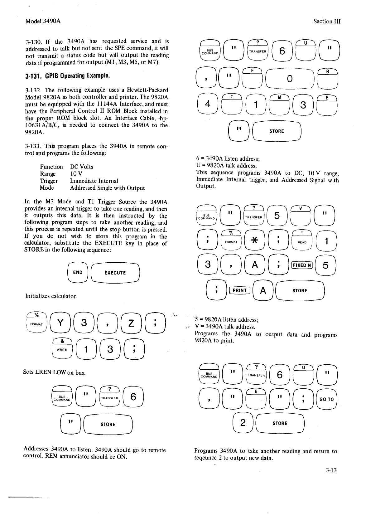
Model3490A
3-130. If the 3490A has requested
service and is
addressed
to talk but not sent the SPE command, it will
not transmit a status code but will output the reading
data
if programmed
for output (Ml, M3, M5, or M7).
3-131.
GPIB
0perating
ExamPle.
3-132. The following example uses
a Hewlett-Packard
Model 9820A as
both controller
and
printer.
The
98204
must be equipped
with the lll44a Interface,
and
must
have the Peripheral Control II ROM Block installed in
the proper ROM block slot. An Interface Cable, -hp-
lO63lAlBlC, is needed to connect
the 3490A to the
9820A.
3-133. This program places
the 3940A in remote con-
trol and programs the following:
Function DC Volts
Range l0 V
Trigger Immediate Internal
Mode Addressed
Single with Output
In the M3 Mode and Tl Trigger Source the 3490A
provides an internal trigger to take one
reading,
and then
it outputs this data. It is then instructed by the
following program steps to take another reading, and
this proces is repeated
until the stop button is pressed.
If you do not wish to store this program in the
calculator, substitute the EXECUTE key in place of
STORE in the following sequence:
EXECUTE
Initializes
calculator.
Section III
@o@@üo
ooü f-R-\
(r
f-E\
@üoü@
STORE
6 = 3490A
listen
address;
U = 9820A
talk address.
This sequence
programs 3490A
Immediate
Internal trigger,
and
Output.
to DC, 10V range,
Addressed
Signal with
üo
r-'\
rrui
r;l
IFIXEDNI[1J
@o@@
O13@O
@o@o
OrPR'Nrr@[ STORE
'5 = 9820A listen
address;
V = 349OA
talk address.
Programs
the 34904 to output data and programs
9820A to print.
r?. rfi
\coMMANO/ \ I
\--l
["]{
LJ\-
Addresses
3490A to listen.
3490A should
so to remote
control. REM annunciator
should
be
ON.
oaoo@
lersl
sy
Irl
o@@üo
STORE
Programs
3490A to take
another
reading
and
return to
seqeunce
2 to output new
data.
0
@o@o@o
@o@o
Sets
LREN
LOW
on
bus.
STORE
3-1
3
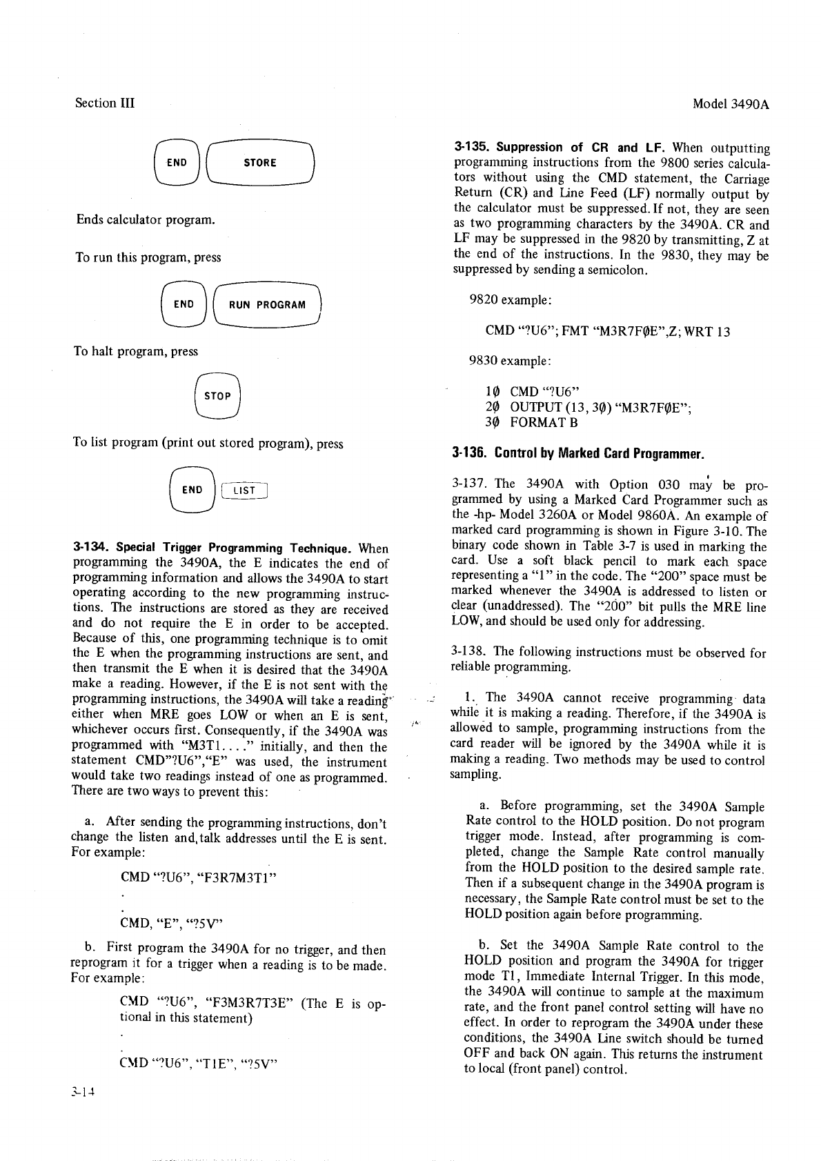
STORE
To halt
program, press
-
I sroP
l
L-J
To list program
(print out stored program),
press
I END
ll Ltsr
\/
Section
III
Ends
calculator
program.
To run this
program, press
10
20
3Q
3-134. Special Trigger Programming
Technique.
When
programming the 3490A, the E indicates the end of
programming information and allows
the 3490A to start
operating according to the new programming instruc-
tions. The instructions are stored as they are received
and do not require the E in order to be accepted.
Because
of this, one programming
technique is to omit
the E when the programming
instructions are sent, and
then transmit the E when it is desired that the 3490A
make a reading. However, if the E is not sent with the
programming
instructions, the 34904 will take a readin!"
either when MRE goes LOW or when an E is sent,
whichever
occurs
first. Consequently,
if the 3490A was
progammed with "M3Tl. . . ." initially, and then the
statement CMD"?U6","E" was used, the instrument
would take two readings
instead
of one
as
programmed.
There
are two ways
to prevent
this:
a. After sending
the programming
instructions, d.on,t
change
the listen and,talk addresses
until the E is sent.
For
example:
CMD
"?U6'" "F3R7M3T1''
öMD,..E,,,
..?5'\P,
b. First program
the 34904 for no trigger,
and then
reprogram
it for a trigger
when
a reading
is to be
made.
For example:
CMD "?U6", "F3M3R7T3E', (The E is op-
tional
in this
statement)
Model 3490A
3-135. Suppression
of CR and LF. When outputting
programming
instructions
from the 9800 series
calcula-
tors without using the CMD statement, the Carriage
Return (CR) and Line Feed (LF) normally output by
the calculator
must be suppressed. If not, they are seen
as two programming
characters
by the 3490A. CR and
LF may be suppressed
in the
9820 by transmitting,Z at
the end of the instructions.
In the 9830,
they may be
suppressed
by sending
a
semicolon.
9820
example:
CMD
"?U6";FMT "M3R7FQE",Z;WRT
13
9830 example:
CMD
"?U6''
OUTPUT
(13,
30)
..M3R7F@E";
FORMAT
B
3-136. Controlby
Marked
Card Programmer.
3-137. The 34gOA with Option 030 maj, be pro-
grammed
by using
a Marked Card Programmer
such
as
the -hp-
Model 3260A or Model 9860A. An example
of
marked
card programming
is shown in Figure
3-10.
The
binary code shown
in Table 3-7 is used in marking
the
card. Use a soft black pencil to mark each space
representing
a
"l" in the code. The
"200" space
must
be
marked whenever
the 3490A is addressed
to listen or
clear
(unaddressed).
The "200" bit pulls the MRE line
LOW,
and should
be used
only for addressing.
3-138. The following instructions
must be observed
for
reliable
programming.
.j 1. The 3490A cannot receive programming data
whilö it is making
a reading. Therefoie,
if tn. :+gOR i,
allowtid
to sample, programming
instructions
from the
card reader
will be ignored by the 3490A while it is
making
a reading.
Two methods
may be used
to control
sampling.
a. Before programming,
set the 3490A Sample
Rate
control to the HOLD position.
Do not program
trigger mode. Instead, after programming
is com-
pleted, change
the Sample Rate control manually
from the HOLD position to the desired sample
rate.
Then
if a subsequent
change
in the 3490A program
is
necessary,
the Sampie
Rate
control must
be
set to the
HOLD position again
before programming.
b. Set the 3490A Sample Rate control to the
HOLD position and program
the 3490A for trigger
mode T1
, Immediate
Internal
Trigger.
In this mode,
the 3490A will continue to sample
at the maximum
rate, and the front panel
control setting
will have no
effect.
In order to reprogram
the 34904 under these
conditions,
the 3490A Une switch should
be tumed
OFF and back
ON again. This
returns the
instrument
to local (front panel)
control.
-1-ll
c\tD
"?u6",
..TlE",,.?5V"
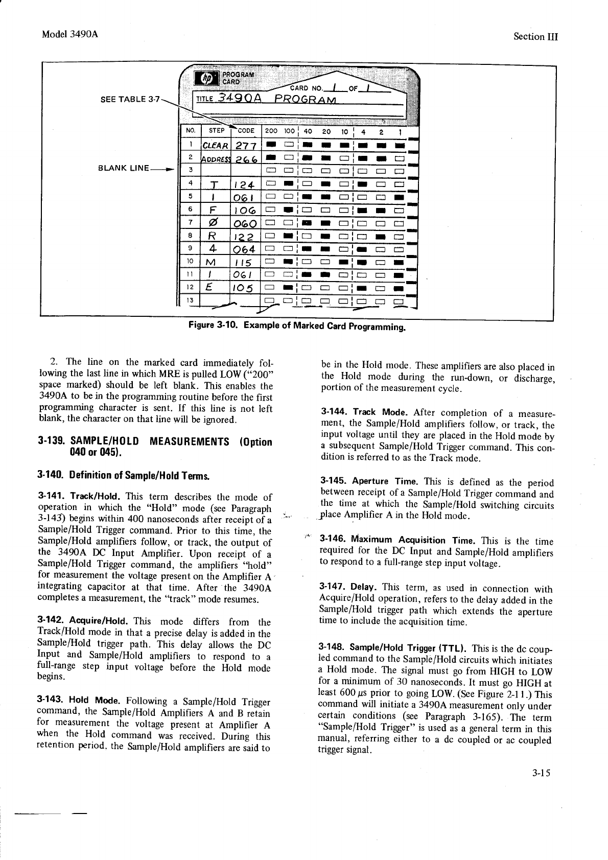
Model
3490A
Figure 3-10. Example
of Marked
Card
programming.
Section
III
2. The line on the marked card immediately fol-
lowing the last
line in which MRE is pulled LOW (,,200-
space
marked) should be left blank. This enables
the
3490A to be
in the programming
routine before the first
programming character is sent. If this line is not left
blank, the character
on that line will be ignored.
3-139.
SAMPLE/H0LD
MEASUREMENTS
(0ption
040
or 045).
3-140.
Definition
of
Sample/Hold
Terms
3-141. Track/Hold. This term describes
the mode of
operation in which the "Hold" mode (see paragraph
3-14, begins
within 400 nanoseconds
after receipt
oi a
Sample/Hold
Trigger
command.
Prior to this time, the
Sample/Hold amplifiers follow, or track, the output of
the 34904 DC Input Amplifier. Upon receipf of a
SampleiHold
Trigger
command, the amplifiers
..hold"
for measurement
the voltage present
on the Amplifier A
integrating capacitor at that time. After the 3490A
completes
a
measurement,
the .track,'mode resumes.
3-142. Acquire/Hold. This mode differs from the
Track/Hold
mode
in that a precise
delay is
added
in the
Sample/Hold
trigger path. This delay allows the DC
lnput and Sample/Hold amplifiers to respond to a
full-range step input voltage before the Äold mode
begins.
3-143. Hold Mode. Following a Sample/Hold
Trigger
command,
the Sample/Hold
AmplifierJ A and B retain
Ior measurement
the voltage present
at Amplifier A
when the Hold command was received.
During this
retention
period.
the Sample/Hold
amplifiers
are said to
be in the Hold mode.
These
amplifiers
are
also placed
in
the Hold mode during the run-down, or discharge,
portion
of the
measurement
cycle.
3-1u14.
Track Mode. After completion of a measure_
ment, the Sample/Hold
amplifiers
follow, or track, the
input voltage
until they are
placed
in the
Hold mode
by
a subsequent
Sample/Hold
Trigger
command.
This con_
dition
is
referred
to as the Track
mode.
3-145. Aperture Time. This is defined as the period
between
receipt
of a Sample/Hold
Trigger
command
and
the time at which the Sample/Hold switching circuits
.place
Amplifier A in the Hold mode.
F 3-146.
Maximum Acquisition
Time. This is the time
required
for the DC Input and Sample/Hold
amplifiers
to respond
to a full-range
step
input voltage.
3-147. Delay. This term, as used
in connection with
Acquire/Hold
operation,
refers
to the
delay
added
in the
Sample/Hoid
trigger path which extends
the aperture
time
to include
the
acquisition
time.
3-148. Sample/Hold
Trigger
(TTL). This is
the dc coup
led
command
to the Sample/Hold
circuits
which
initiates
a Hold mode. The sigral must go from HIGH to LOW
for a minimum of 30 nanoseconds.
It must go HIGH at
least
600ps prior to going
LOW.
(See
Figure
2-l l.) This
command
will initiate
a 3490A
measurement
only under
certain conditions (see Paragraph
3-165). The term
"Sample/Hold
Trigger" is
used
as
a general
term in this
manua.l,
referring
either to a dc coupled
or ac
coupled
trigger
signal.
SEE
TABLE
3.7
BLANK LINE+
rffi'slisli r.l.i...l*jiiä='8ffifr
lrrruE
349OA PRoonnvr ],'ir
NO. )tEr co0E zoo rool40
zo rol + z I
IiLEAR 27-l r Ei! r rir r r
2C.C, lfl r r alr r c=
3EE
-I
E El =!n E c=
T,21 C:I
06l Etrf r r EIE trf r
FtoG EI
60,60 -- E r EIt:] E [f
IRt22 EI -rtrlitrfIfl
94o64 EE r r c:lr E r:
to Mt5 E=I .EI
ll I06t EE tlcf E:] ff I
l? Eto5 -}EE IT:I
13 -l- -l-
UIUUU
--
3-l 5
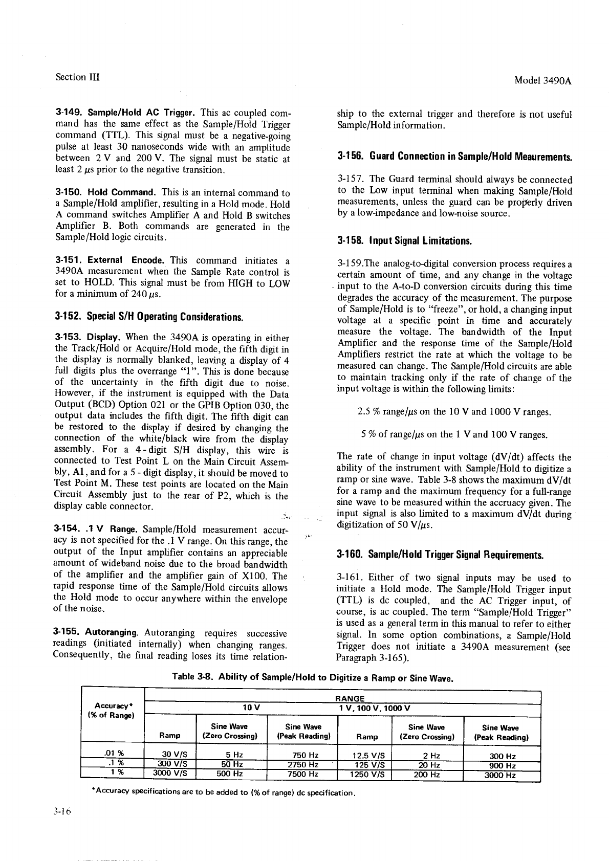
Section III
3-149. Sample/Hold
AC Trigger. This ac
coupled
com-
mand has the same
effect as the Sample/Hold
Trigger
command (TTL). This signal must be a negative-going
pulse
at least 30 nanoseconds
wide with an amplitude
between 2Y and 200
V. The signal
must be static at
least
2 ps prior to the negative transition.
3-150. Hold Command.
This
is
an intemal
command
to
a Sample/Hold
amplifier,
resulting
in a Hold mode.
Hold
A command switches
Amplifier A and Hold B switches
Amplifier B. Both commands are generated
in the
Sample/Hold
logic
circuits.
3-151. External Encode.
This command initiates a
3490A measurement
when the Sample Rate control is
set to HOLD. This signal
must be from HIGH to LOW
for a minimum of 240
ps.
3-152. Special
S/H 0perating
Gonsiderations.
3-153. Display. When
the 3490A is operating in either
the Track/Hold or Acquire/Hold mode, the fifth digit in
the display is normally blanked, leaving a display of 4
full digits plus the overrange
"1". This
is done
because
of the uncertainty in the fifth digit due to noise.
However,
if the instrument
is equipped
with the Data
Output (BCD) Option 021 or the GPIB
Option
030, the
output data includes the fifth digit. The fifth digit can
be restored to the display if desired by changing
the
connection of the white/black wire from the display
assembly. For a 4 - digit S/H display, this wire is
connected to Test Point L on the Main Circuit Assem-
bly, Al, and
for a 5
- digit
display, it should
be moved to
Test Point M. These
test points are located on the Main
Circuit Assembly
just to the rear of P2, which is the
display
cable
connector. -._"
3-154. .1 V Range.
Sample/Hold
measurement
accur-
acy is not specified
for the .l V range.
On
this
range,
the
output of the Input amplifier contains
an appreciable
amount of wideband
noise
due to the broad
bandwidth
of the amplifier and the amplifier gain of X100. The
rapid response
time of the Sample/Hold circuits allows
the Hold mode to occur anywhere
rvithin the envelope
of the noise-
3-155. Autoranging.
Autoranging requires successive
readings (initiated internally) when changing ranges.
Consequently,
the final reading
loses
its time relation-
Model34904
ship to the extemal trigger and therefore is not useful
Sample/Hold
information.
3-156. Guard
Connection
in
Sample/Hold Meaurements.
3-157. The Guard terminal
should
always be
connected
to the Low input terminal when making Sample/Hold
measurements,
unless
the guard can be properly driven
by a low-impedance
and low-noise
source.
3-158.
Input
Signal Limitations.
3-1 59.The
analog-to-digital
conversion process
requires
a
certain amount of time, and any change in the voltage
input to the A-to-D conversion
circuits during this time
degrades
the accuracy of the
measurement. The purpose
of Sample/Hold
is to "fresze", or hold, a changing
input
voltage at a specific point in time and accurately
measure the voltage. The bandwidth of the Input
Amplifier and the response time of the Sample/Hold
Amplifiers restrict the rate at which the voltage to be
measured can
change. The Sample/Hold circuits
are able
to maintain tracking only if the rate of change
of the
input voltage
is within the follo,wing limits:
2.5
%rangelps
on the
l0 V and 1000
V ranges.
5
%
of rmgelps on the I V and 100 V ranges.
The rate of change
in input voltage (dv/dt) affects the
ability of the instrument with SampleiHold to digitize a
ramp
or sine
wave. Table 3-8 shows the maximum dV/dt
for a ramp and the maximum frequency for a full-range
sine
wave to be measured
within the accruacy
given.
The
input signal is also limited to a maximum dV/dt during
digitization
of 50 V/ss.
3-160. Sample/Hold Trigger
Signal
Requirements.
3-161. Either of two signal inputs may be used to
initiate a Hold mode. The Sample/Hold Trigger
input
(TTL) is dc coupled, and the AC Trigger input, of
course,
is ac coupled.
The term "Sample/Hold
Trigger"
is used
as
a general
term
in this
manual to refer to either
signal.
tn some option combinations,
a Sample/Hold
Trigger does not initiate a 3490A measurement
(see
Paragraph
3-165).
Table
3-8. Ability of Sample/Hotd
to Digitize
a Ramp
or Sine Wave.
Acc|Jracy*
(% of Rangef
BANGE
10v 1 V,
100
V,
1000
v
Ramp Sine Wave
lZero Crossing) Sine Wave
(Peak
Reading) Ramp Sine Waw
(Zero Crossing) Sine Wave
{Peak Reading)
.01
%30 v/s 5Hz 75O
Hz 12.5
V
lS 2Hz 3OO Hz
1% 300
v/s 5O
Hz 275O
Hz 125 V/S 20 Hz 90O
Hz
1% 3000
v/s 5O0 Hz 75OO
Hz 1250 V/S 2OO Hz 3ü)O Hz
*Accuracy specifications
are to be added to (%
of range)
dc specification.
-1-l o
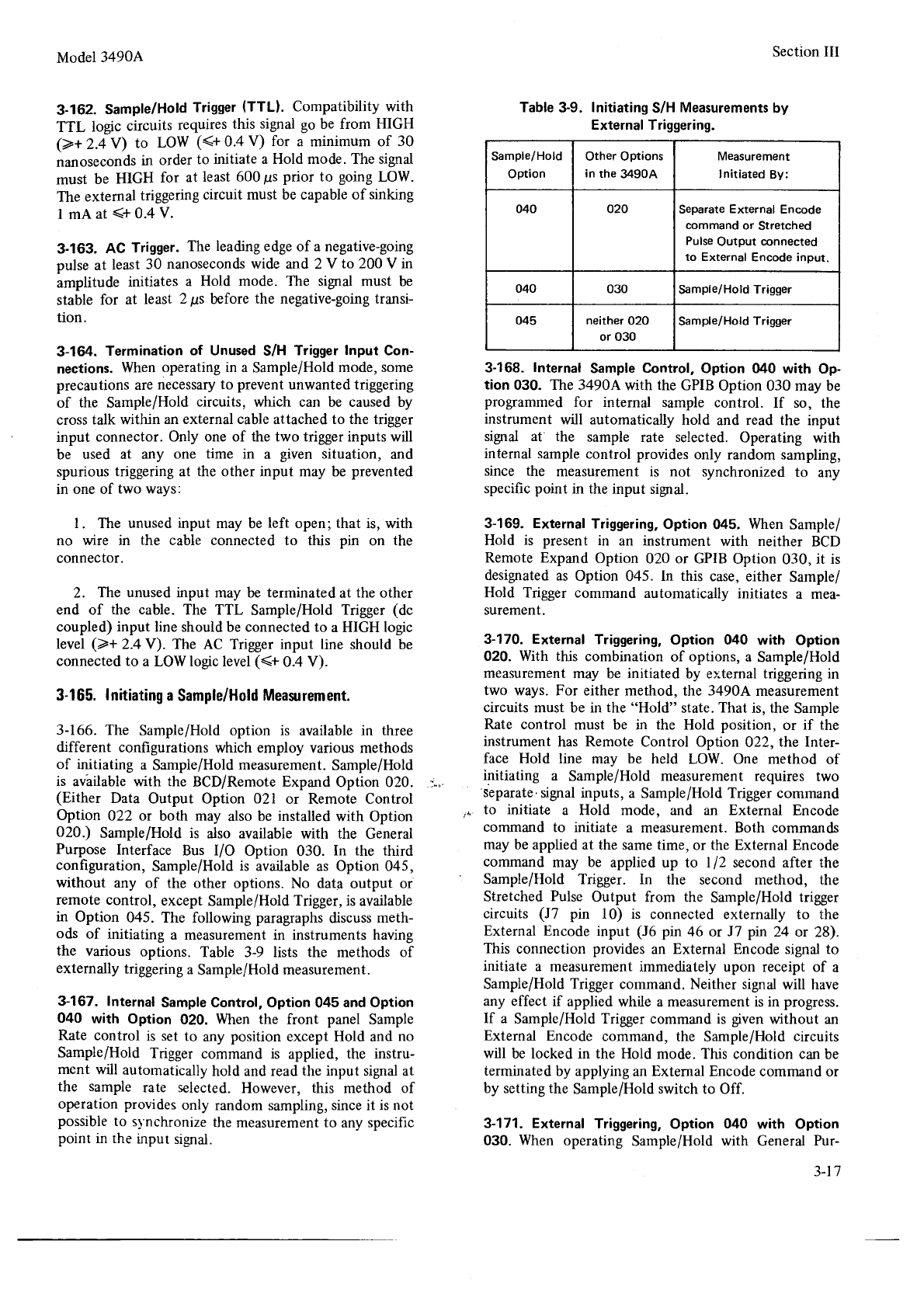
Model3490A
3-162. Sample/Hold
Trigger
(TTL). Compatibility with
TTL logic circuits
requires
this signal
go
be from HIGH
(>+ 2.4
V) to LOW ((+ 0.4
V) for a minimum of 30
nanoseconds
in order
to initiate a Hold mode. The signal
must be HIGH for at least
600
ps prior to going
LOW.
The external triggering
circuit must be capable of sinking
I mA at (+ 0.4 V.
3-163. AC Trigger.
The leading
edge of a negative-going
pulse
at least
30 nanoseconds wide and 2 V to 200
V in
amplitude initiates a Hold mode. The sigral must be
stable for at least 2 ps before the negative-going transi-
tion.
3-164. Termination of Unused
S/H Trigger
Input Con-
nections.
When
operating in a Sample/Hold
mode, some
precautions
are
necessary
to prevent
unwanted triggering
of the SampleiHold circuits, which can be caused by
cross
talk within an external cable
attached
to the trigger
input connector. Only one of the two trigger inputs
will
be used at any one time in a given situation, and
spurious
triggering
at the other input may be prevented
in one of two ways:
l. The unused
input may be left open; that is, with
no wire in the cable connected to this pin on the
connector.
2. The unused input may be terminated
at the other
end of the cable. The TTL Sample/Hold
Trigger
(dc
coupled)
input line should be connected to a HIGH logic
level ()+ 2.4V). The AC Trigger
input line should be
connected to a LOW logic level
(<+ 0.4 V).
3-165.
Initiating
a
Sample/Hold
Measurement.
3-166. The Sample/Hold option is available
in three
different configurations which employ various methods
of initiating a Sample/Hold
measurement.
SampleiHold
is aväilable with the BCD/Remote Expand Option 020.
(Either Data Output Option 021 or Remote Control
Option 022 or both may also
be installed
with Option
020.) Sample/Hold is also available
with the General
Purpose Interface Bus I/O Option 030. In the third
con{iguration,
Sample/Hold
is available as Option 045,
without any of the other options. No data output or
remote control, except
Sample/Hold
Trigger, is
available
in Option 045. The following paragraphs
discuss
meth-
ods of initiating a measurement in instruments having
the various options. Table 3-9 lists the methods of
externally
triggering
a
Sample/Hold measurement.
3-167. Internal
Sample Control, Option
045 and Option
040 with Option 020. When the iront panel Sample
Rate control is set
to any position
except Hold and no
Sample/Hold Trigger
command is applied, the instru-
ment will automatically
hold and read
the input signal
at
the sample rate selected.
However, this method of
operation provides
only random sampling, since it is not
possible
to s1'nchronize
the
measurement to any
specific
point in the input signal.
Section III
Table
3-9. Initiating
S/H Measurements
by
External Triggering.
Sample/Hold
Option
Other Options
in
the
34904
Measurement
Initiated By:
o40 o20 Separate
External Encode
command or Stretched
Pulse
Output connected
to External Encode input.
040 030 Sample/Hold Trigger
045 neither 020
or O30
Sample/Hold Trigger
3-168. Internal Sample
Control, Option 040 with Op-
tion 030. The 3490A
with the GPIB
Option 030 may
be
programmed
for internal sample control. If so, the
instrument will automatically
hold and read the input
signal at the sample rate selected.
Operating with
internal sample
control provides
only random sampling,
since the measurement is not synchronized to any
specific point in the
input signal.
3-169. External
Triggering,
Option 045. When
Sample/
Hold is present in an instrument with neither BCD
Remote
Expand Option 020 or GPIB
Option 030, it is
designated
as Option 045. In this case, either Sample/
Hold Trigger command automatically
initiates a mea-
surement.
3-170. External Triggering,
Option 040 with Option
020. With this combination
of options,
a Sample/Hold
measurement
may be initiated by external triggering in
two ways. For either
method, the 34904 measurement
circuits
must be in the "Hold" state.
That
is, the Sample
Rate control must be in the Hold position, or if the
instrument
has Remote
Control Option 022, the lnter-
face Hold line may be held LOW. One method of
initiating a Sample/Hold measurement requires two
'separate
signal inputs,
a Sample/Hold Trigger command
," to initiate a Hold mode, and an External Encode
command to initiate a measurement. Both commands
may be
applied at the same time,
or the
External Encode
command
may be applied up to ll2 second after the
Sample/Hold Trigger. In the second method, the
Stretched Pulse
Output from the Sample/Hold
trigger
circuits (J7 pin 10) is connected externally to the
External Encode input (J6 pin 46 or J7 pin 24 or 28).
This connection provides
an External Encode signal to
initiate a measurement immediately
upon receipt of a
Sample/Hold Trigger command. Neither signal
will have
any effect if applied while a measurement is in progress.
If a Sample/Hold Trigger command is given
without an
External Encode command, the Sample/Hold
circuits
will be locked in the Hold mode. This condition can
be
terminated
by applying
an
External
Encode command or
by setting the Sample/Hold switch to Off.
3-171. External
Triggering,
Option 040 with Option
030. When operating Sample/Hold with General
Pur-
3-t7
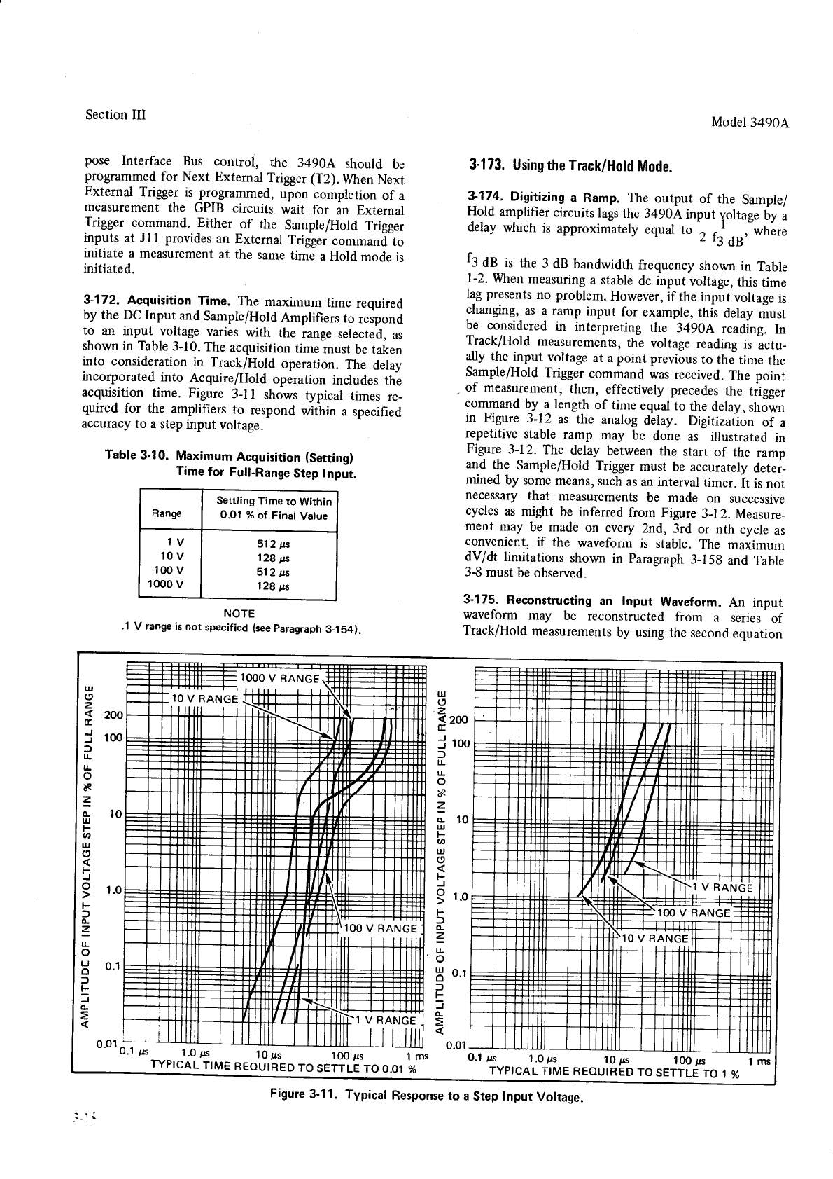
Section III
pose Interface Bus controi, the 3490A should be
programmed
for Next External Trigger
(T2). When
Next
External Trigger is programmed, upon completion of a
measurement the GPIB circuits wait for an External
Trigger command. Either of the Sample/Hold Trigger
inputs at Jll provides
an External
Trigger
command
to
initiate a measurement
at the same
time a Hold mode is
initiated.
3-172. Acquisition
Time. The maximum
time required
by the DC Input and
Sample/Hold
Amplifiers
to respond
to an input voltage varies with the range selected.
as
shown in Table
3-10.
The
acquisition
time-must
be taien
into consideration in Track/Hold operation. The delay
incorporated into Acquire/Hold operation includes thl
acquisition time. Figure 3-l I shows typical times re_
quired for the amplifiers to respond within a specified
accuracy
to a
step
input voltage.
Table
3-10. Maximum
Acquisition
(Settingl
Time
for Full-Range
Step Input.
Model3490A
3-173.
Using
the Track/Hold
Mode.
3-174. Digitizing
a Ramp. The output of the Sample/
Hold amplifier
circuits
lags
the 3490|input yoltage
by a
delay which is approximately equal to " " I , where
L 13dB
f: On ir the 3 dB bandwidth frequency shown in Table
l-2. When
measuring
a stable
dc input voltage,
this
time
lag presents
no problem.
However,
if the
input voltage
is
changing,
as a ramp input for example,
thii delay must
be considered
in interpreting the 34gOA
reading. In
Track/Hold measurements,
the voltage
reading
is actu_
ally the input voltage
at a point previous
to the time the
Sample/Hold
Trigger
command
was
received.
The point
of measurement,
then, effectively
precedes
the trigger
command
b-y
a length of time equal
to the delay,
shown
in Figure 3-12 as the analog dähy. Digitization of a
repetitive
stable
ramp may be done as illustrated in
Figure
3-1
2. The delay between
the start of the ramp
and the Sample/Hold
Trigger
must be accurately
detei_
mined
by some
means,
such
as
an interval
timer.
It is not
necessary
that measurements
be made on successive
cycles
as
might be inferred
from Figure
3-12.
Measure-
ment may be made
on every 2nd, 3rd or nth cycle
as
convenient,
if the waveform is stable.
The maximum
dv/dt limitations shown
in paragraph
3-l5g and Table
3{ must
be observed.
3-175. Reoonstructing
an Input Waveform.
An input
waveform may be reconstructed from a series of
Track/Hold
measurements
by using the
second
equation
Range
Settling Time to Within
0.01 % of Final Vatue
1V
10v
100
v
1000
v
512 tts
128
ps
512 ps
128
ps
NOTE
.1
V range
is
not
specified
(see
paragraph
3-1541.
uJ
(9
z
tr
J
J
tt
tJ-
a
=
uJ
F
at,
lrJ
o
F
J
F
=
t!
UJ
a
E
J
200
100
.lLl
.z
(r
J
J
f
IL
o
öR
=
o-
LIJ
F
.tt
Ll,
(9
F.
J
o
F
f,
=
tJ.
o
uJ
n
t-
=
o-
200
100
10
1.0
0.1
to
1.0
0.1
1
V
RANGE
6.6t
^
u.l ,,rs 1.0ps IOps IOOps lms
TYPICAL
TIME
REOUIRED
TO
SETTLL
TO O.OT
X
0.o1
0.1
lrs 1.0
rrs 10,/s 100
rc
TYPICAL
TIME
REOUIRED
TO
SETTLETO
1
%
Figure
3-1
1. Typicat
Response
to a
Step Input
Voltage.
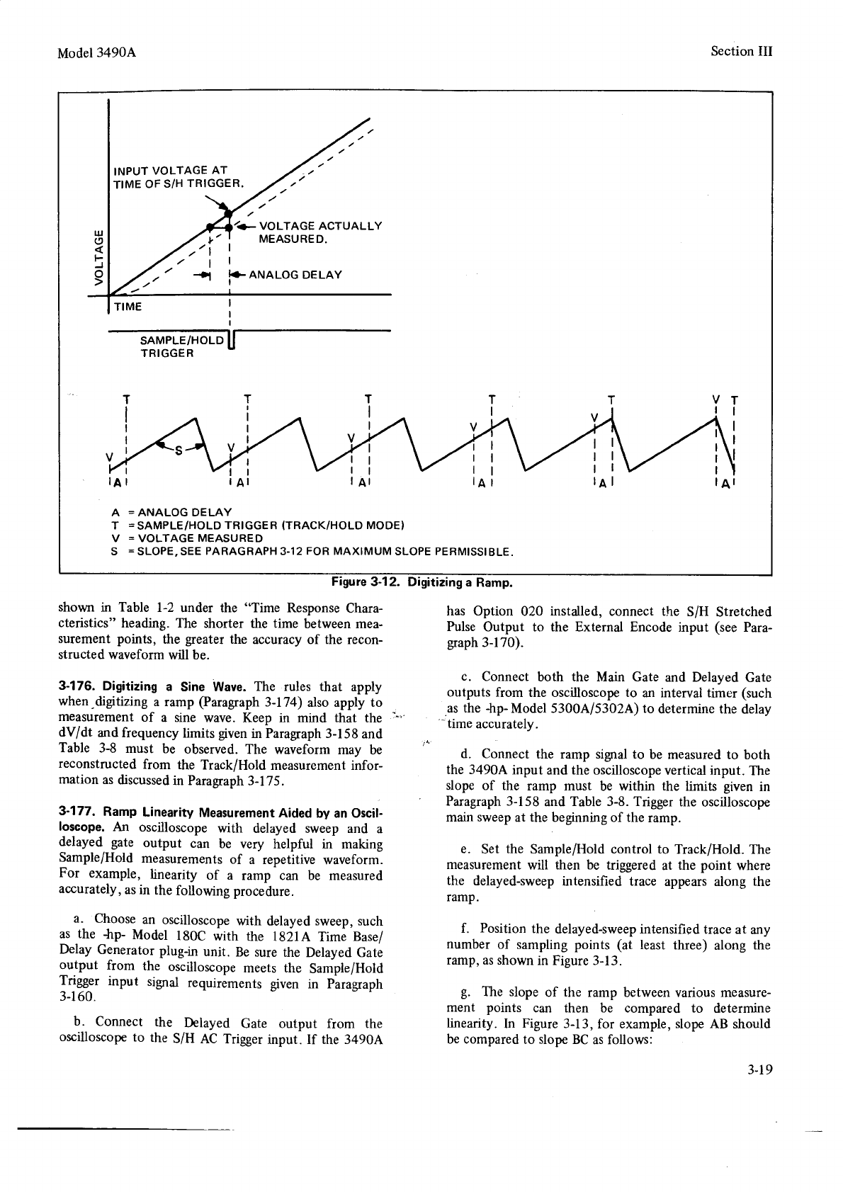
Model3490A
shown in Table l-2 under the "Time Response
Chara-
cteristics" heading. The shorter the time between mea-
surement points, the greater
the accuracy of the recon-
structed waveform will be.
3-176. Digitizing a Sine Wave.
The rules that apply
when-digitizing a ramp @aragraph
3-174) also apply to
measurement
of a sine wave. Keep in mind that the
dV/dt and
frequency limits given
in Paragraph 3-158 and
Table 3{ must be observed.
The waveform may be
reconstructed from the Track/Hold measurement infor-
mation
as
discussed
in Paragraph
3-175.
3-177. Ramp Linearity
Measurement
Aided by an Oscil-
loscope. An oscilloscope with delayed sweep and a
delayed gate output can be very helpful in making
Sample/Hold measurements
of a repetitive waveform.
For example, linearity of a ramp can be measured
accurately,
as in the
following
procedure.
a. Choose
an oscilloscope
with delayed
sweep, such
as the {rp- Model l80C with the l82lA Time Base/
Delay Generator
plug-in unit. Be sure the Delayed Gate
output from the oscilloscope
meets the Sample/Hold
Tdry:. input signal requirements given in päragraph
3-l
60.
b. Connect the Delayed Gate output from the
oscilloscope
to the S/H AC Trigger
input. lf the 3490A
has Option 020 installed,
connect the S/H Stretched
Pulse Output to the External Encode input (see Para-
graph
3-170).
c. Connect both the Main Gate and Delayed
Gate
outputs from the oscilloscope to an interval timer (such
as the -hp-Model5300Al53O2A)
to determine the delay
time
accurately.
d. Connect
the ramp sigral to be measured
to both
the 3490A input and the oscilloscope
vertical
input. The
slope of the ramp must be within the limits given in
Paragraph 3-158
and
Table 3-8. Trigger
the oscilloscope
main sweep
at the beginning of the
ramp.
e. Set the SampleiHold control to TrackiHold. The
measurement
will then be triggered at the point where
the delayed-sweep
intensified trace appears along the
ramp.
f. Position
the delayed-sweep intensified
trace at any
number of sampling points (at least three) along the
ramp, as shown
in Figure 3-13.
g. The slope
of the ramp between various measure-
ment points can then be compared to determine
linearity. ln Figure
3-13,
for example, slope AB should
be compared
to slope BC
as follows:
Section III
TNPUT
VOLTAGE
AT
TIME
OF
S/H
TRIGGER,
t
/l
/l
VOLTAGE ACTUALLY
MEASURED.
I
I
I
IAr
A
T
V
S
=
ANALOG DELAY
=
SAMPLE/HOLD
TRIGGER
(TRACK/HOLD
MODE)
=
VOLTAGE
MEASURED
=
SLOPE, SEE
PARAGRAPH
3-12
FOR
MAXIMUM
SLOPE
PERMISSIBLE.
Figure
3-1 2. Digitizing
a Ramp.
3-r9
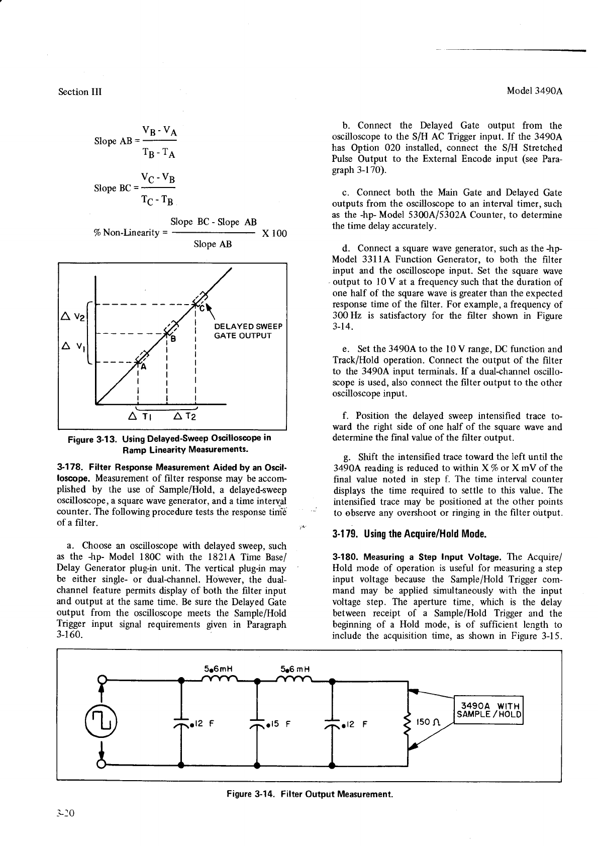
Section III
vs-ve
Slope AB = -
Ts-Ta
Vc
-vs
Slope
BC
= -
Tc-Ts
Slope
BC
- Slope
AB
%
Non-Linearity =x 100
Slope
AB
Figure
3-13. Using
Delayed-Sweep
Oscilloscope
in
RamP
LinearitY
Measurements.
&178. Filter Response Measurement
Aided by an Oscil-
loscope.
Measurement
of filter response may be accom-
plished by the use of Sample/Hold, a delayed-sweep
oscilloscope,
a square
wave
generator,
and a time interv-al
counter. The following procedure
tests the response
tiniö
ofa filter.
a. Choose
an oscilloscope with delayed
sweep,
such
as the -hp- Model l80C with the 1821A Time Base/
Delay Generator plug-in unit. The vertical plug-in may
be either single- or dual-channel. However, the dual-
channel feature permits display of both the filter input
and output at the same time. Be
sure
the Delayed
Gate
output from the oscilloscope meets the Sample/Hold
Trigger input signal requirements given in Paragraph
3-1
60.
Model3490A
b. Connect the Delayed Gate output from the
oscilloscope to the S/H AC Trigger
input. If the 3490A
has Option 020 installed, connect the S/H Stretched
Pulse Output to the Extemal Encode input (see Para-
graph
3-170).
c. Connect both the Main Gate and Delayed
Gate
outputs from the oscilloscope
to an interval timer, such
as the -hp-
Model 5300A15302A
Counter,
to determine
the time delay accurately.
d. Connect a square wave
generator,
such
as
the -hp-
Model 33llA Function Generator,
to both the filter
input and the oscilloscope input. Set the square wave
output to l0 V at a frequency such that the duration of
one half of the square wave is greater
than the expected
response
time of the filter. For example, a frequency
of
300 Hz is satisfactory for the filter shown in Figure
3-14.
e. Set the 3490A
to the l0 V range, DC function and
Track/Hold operation.
Connect
the output of the filter
to the 3490A input terminals. If a dual-channel oscillo-
scope is used, also connect the hlter output to the other
oscilloscope input.
f. Position the delayed sweep intensified trace to-
ward the right side of one half of the square
wave
and
determine
the final value of the filter output.
g. Shift the intensified trace toward the left until the
3490A reading
is reduced
to within XVo or X mV of the
final value noted in step f. The time interval counter
displays the time required to settle to this value. The
intensified
trace may be positioned
at the other points
to observe
any overshoot
or ringing
in the
filter oütput.
3-179.
Using the Acquire/Hold Mode.
3-180. Measuring a Step Input Voltage. The Acquire/
Hold mode of operation
is useful for measuring
a step
input voltage because
the Sample/Hold Trigger com-
mand may be applied simultaneously
with the input
voltage step. The aperture time, which is the delay
between receipt of a Sample/Hold Trigger and the
beginning of a Hold mode, is of sufficient length to
include the acquisition
time, as
shown
in Figure 3-l 5.
5o6mH
3490A W|TH
SAMPLE
/HOLD
5e6
mH
,"1
",1
A
A
DELAYED SWEEP
GATE OUTPUT
_1-10
Figure
3-14. Filter
Output
Measurement.
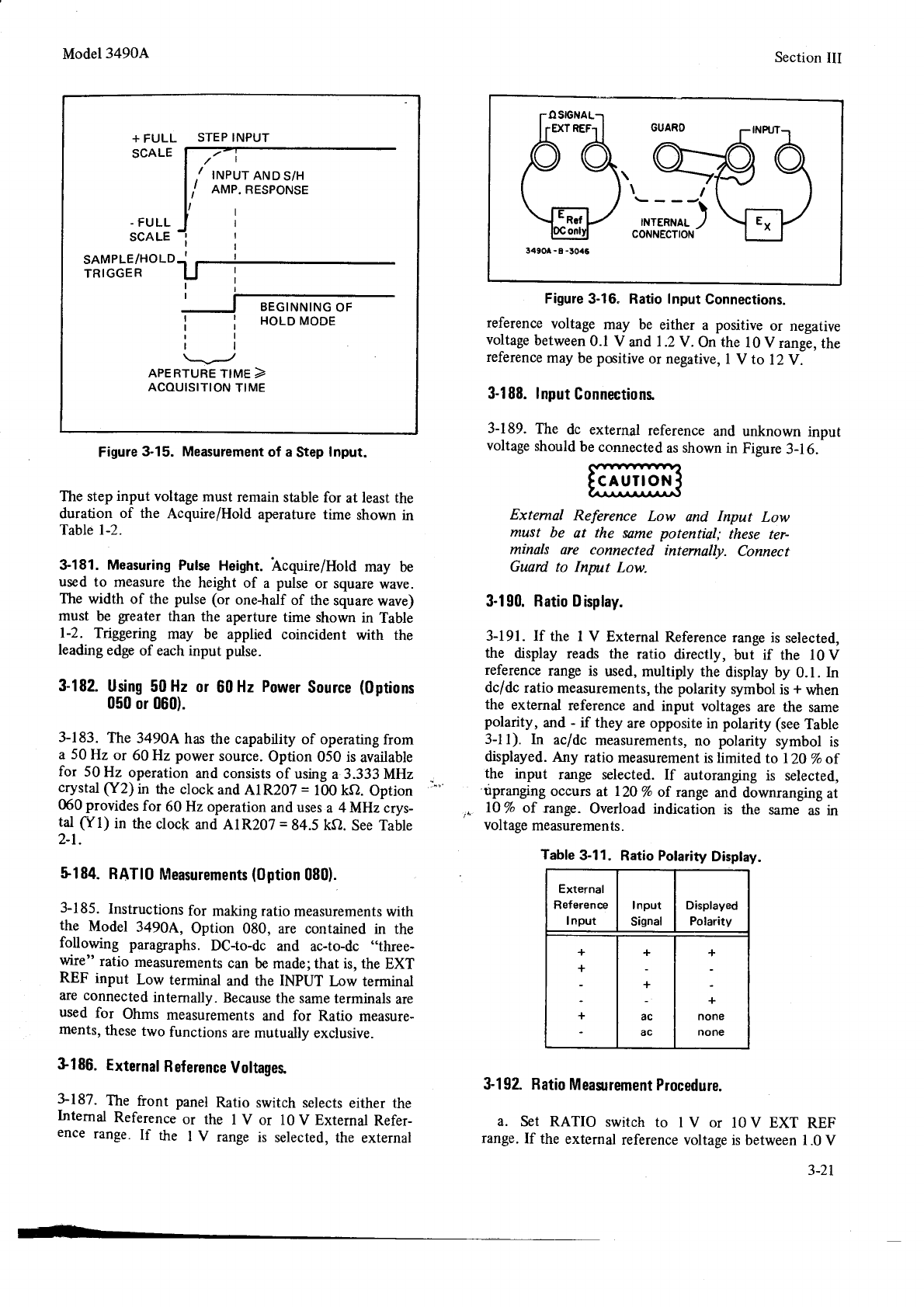
Model3490A
The step
input voltage
must remain stable
for at least
the
duration of the Acquire/Hold aperature time shown in
Table 1-2.
3181. Measuring
Pulse
Height.
hcquire/Hold may be
used to measure
the height of a pulse or square
wave.
The width of the pulse (or one-half
of the square
wave)
must be greater than the aperture time shown in Table
l-2. Triggering may be applied coincident with the
leading
edge
of each input pulse.
3-182.
Using
50
Hz
or 60
Hz
Power
Source
(Options
050
or 060).
3-183. The 3490A has
the capability
of operating
from
a 50
Hz or 60 Hz power
source.
Option 050 is available
for 50 Hz operation
and consists
of using
a 3.333 MHz
crystal
(Y2) in the clock
and AlR207 = 100 kSr.
Option
060 provides
for 60 Hz operation
and
uses
a 4 MHz crys-
tal CYI) in the
clock and
AlR207 = 84.5 kQ. See Table
2-1.
$184.
RATIO
lf'leasurements
(0ption
080).
3185. Instructions
for making ratio
measurements
with
the Model 3490A, Option 080, are contained in the
following paragaphs. DC-to-dc and ac-to-dc ..three-
wire" ratio measurements
can be made; that is, the EXT
REF input Low terminal and the INPUT Low terminal
are connected
intemally. Because
the same
terminals
are
used for Ohms measurements
and for Ratio measure-
ments,
these
two functions are
mutually exclusive.
$186.
External
Beference
Voltages.
3187. The front panel
Ratio switch selects
either the
lntemal Reference
or the I V or l0 V External
Refer-
ence range. If the I V range
is selected, the external
Section
III
3-1 92. Ratio
Measrement
Procedure.
a. Set RATIO switch to I V or l0 V EXT REF
range.
If the external
reference
voltage is between
1.0
V
Figure 3-16. Ratio Input
Connections.
reference
voltage may be either a positive or negative
voltage
between
0.1 V and
1.2Y. On
the l0 V range,
the
reference
may
be
positive
or negative,
I V to l2 V.
3-188. lnput
Connections
3-189. The dc external reference
and unknown input
voltage
should
be
connected
as shown in Fizure
3-16.
External
Reference
I
nput
I
nput
Signal
Displayed
Polarity
+
+
+
+
+
ac
ac
+
+
none
none
Extemal Reference Low and Input Low
must be at the same
potential; these ter-
minals are connected intemally. Connect
Guard to Input Low.
3-190.
Ratio Display.
3-191. Ifthe I V External
Reference
range
is selected,
the display reads the ratio directly, but if the 10 V
reference
range is used, multiply the display by 0.1. In
dc/dc ratio measurements,
the polarity symbol is + vshsn
the external reference
and input voltages
are the same
polarity, and - if they are opposite in polarity (see
Table
3-ll). In ac/dc measurements,
no polarity symbol is
displayed.
Any ratio measurement
is limited to l2O %
of
the input range selected. If autoranging is selected,
'upranging
occurs
at l2O % of rcnge
and downranging
at
lO% of range. Overload indication is the same
as
in
voltage
measurements.
Table
3-11. Ratio Polarity
Display.
STEP INPUT
-
FULL
SCALE
SAMPLE/HOLD
TRIGGER
APERTURE
TIME
>
ACOUISITION
TIME
Figure
3-15. Measurement
of a
Step
Input.
tu
3-21
Section III Model3490A
and' 1.2
V, the I V range
should be used for greater since these terminals
are
connectedinternally.
accuracy.
f. Read ratio display directly if I V EXT REF range
b. Connect External Reference (dc only) to EXT is
selected. If 10V EXT REFrangeisselected,multipiy
REF terminals. display
by 0.1.
c. Select DC or AC FUNCTION to correspond
to
input signal to be
measured. NOTE
d. Set RANGE switch to desired
range
or to AUTO. When
operating in Autorange mode with less
than full-rcale External Reference input
e. Connect input signal
(dc or ac). Input signal
Low (<1 V or 110 V), the
first reading
foiow-
and External Reference
Low must be at same potential, ing
on uprange
will be incotect.
J-L-
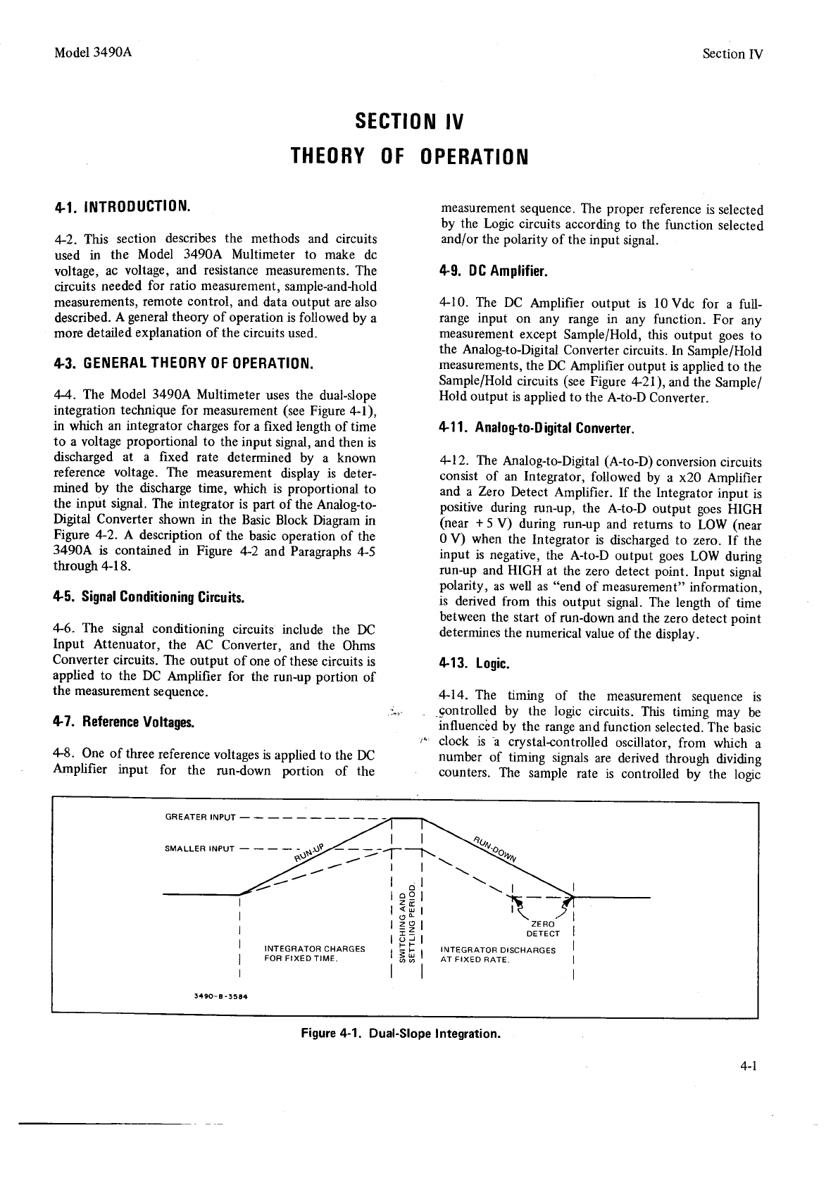
Model
34904 Section
IV
SECTION
IV
THEORY
OF
OPERATION
4I. INTBODUCTION.
42. This section describes the methods and circuits
used in the Model 3490A Multimeter to make dc
voltage, ac voltage, and resistance
measurements.
The
circuits
needed
for ratio measurement,
sample-and-hold
measurements,
remote
control, and data
output are also
described.
A general theory
ofoperation is
followed
by a
more detailed
explanation of the circuits
used.
+3.
GENERAL
THEORY
OF
OPERATION.
44. The Model 34904 Multimeter uses the dual-slope
integration technique for measurement
(see
Figure
4-1),
in which an integrator charges
for a fixed length of time
to a voltage
proportional
to the
input sigral,
and then is
discharged at a fixed rate determined by a known
reference voltage. The measurement display is deter-
mined by the discharge time, which is proportional to
the input sigral. The integrator is part of the Analog-to-
Digital Converter shown in the Basic
Block Dagram in
Figare 4-2. A description of the basic operation of the
3490A is contained in Figure 4-2 and Paragraphs
4-5
through 4-l 8.
45. Signal
Conditioning
Gircuits.
46. The signal conditioning circuits include the DC
Input Attenuator, the AC Converter,
and the Ohms
Converter
circuits.
The output ofone ofthese
circuits is
applied to the DC Amplifier for the run-up portion of
the measurement
sequence.
47. Reference
Voltages.
4-8. One of three
reference
voltages
is applied to the DC
Amplifier input for the run-down portion of the
measurement
sequence.
The
proper
reference
is selected
by the Logic circuits
according
to the function selected
and/or the polarity
of the input signal.
+9. DC Amplifier.
z1-10.
The DC Amplifier output is l0 Vdc for a full-
range input on any range in any function. For any
measurement
except Sample/Hold, this output goes
to
the Analog-to-Digital
Converter circuits. In Sample/Hold
measurements,
the DC Amplifier output is
applied to the
Sample/Hold
circuits
(see
Figure 421), nd the Sample/
Hold output is
applied to the A-to-D
Converter.
4l 1. Analogto-Digital
Converter.
412. The Analog-to-Digital (A-to-D) conversion
circuits
consist
of an Integrator,
followed by a x20 Amplifier
and,
a Zero Detect Amplifier. If the Integrator
input is
positive during run-up, the A-to-D output goes
HIGH
(near + 5 V) during run-up and retums to LOW (near
0 V) when the Integrator
is discharged to zero. If the
input is negative,
the A-to-D output goes
LOW during
run-up and
HIGH at the zero detect
point. Input signal
polarity, as well as
"end of measurement"
information,
is derived from this output signal. The length of time
between
the start ofrun-down and
the zero
detect
point
determines
the numerical
value
of the
display.
413.
Logic.
4-14. The timing of the measurement
sequence
is
. .qontrolled by the logic circuits. This timing may be
influencöd
by the range
and function selected.
The
basic
'"' clock is a crystal-controlled
oscillator,
from which a
number of timing signals
are derived through dividing
counters.
The sample rate is controlled by the logic
GREATER
INPUT
_
SMALLER INPUT
- - - - - .r\?
ßüy
\- RO
INTEGRATOR CHARGES
FOR
FIXED TIME.
INT€GRATOR DISCHARGES
AT FIXED RATE.
3490-8-3584
Figure 4-1. Dual-Slope lntegration.
4-1
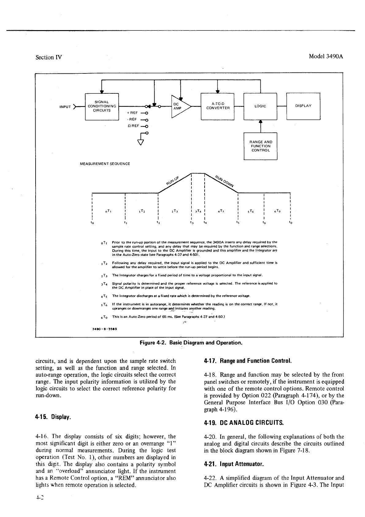
Section
IV
circuits, and is dependent
upon the sample rate switch
setting, as well as the function and range selected. In
auto-range operation, the logic circuits select
the correct
range. The input polarity information is utilized by the
logic circuits
to select the correct reference
polarity for
run-down.
415.
Display.
,1-16.
The display consists
of six digits; however,
the
most significant
digit is either
zero or an overrange
"1"
during normal measurements.
During the logic test
operation
(Test No. 1), other numbers are displayed
in
this dist. The display
also contains a polarity symbol
and an "overload" annunciator light. If the instrument
has
a Remote
Control
option, a "REM" annunciator
also
lights
*tren remote
operation
is selected.
!.
Model3490A
4-17. Range and
Function
Control.
4-18. Range and function may be selected by the front
panel
switches
or remotely,
if the instrument
is equipped
with one of the remote
control
options.
Remote
control
is provided
by Option 022 paragraph
Ll74), or by the
General Purpose Interface Bus I/O Option 030 (Para-
$aph4-196).
+19.
DC
ANAL0G CIRCUITS.
ar20. In general, the following explanations of both the
analog and digital circuits describe
the circuits outlined
in the
block diagram
shown
in Figure
7-18.
421.
lnput Attenuator.
4-22. A simplified diagam of the Input Attenuator
and
DC Amplifier circuits is shown in Figure 4-3. The Input
+REF
<
.REF -{
oREF
{
ll
rl
ll
ll
oTrrrTzlzTr
tl
tl
tr tz
oTr Prior ro the run{p portion ot the m@su.erent sequence,
the 3490A inerts any delay requi.ed by the
smple rate control sening, and any delav rhat may be required by the fundion and range selections.
During lhis time. the input to the DC Amplifier is grounded and this amplifier and the Integrator arc
in lhe Auto-Zero state (see
Para$aphs 4-37 and 4-5O).
tTz Following any delay required, the input signal is applied to the DC Amplifier and sufficient time is
allowed lo. the amplitier to settle belore the run{p period begins.
2
T3 The I ntegrator charges tor a fi xed p6iod of ti me to a rcltage proponional lo the input rignal .
3Ta Signal pola.iry is determined and the prop€r referen@ wltage is plected- The relerence is applied to
rhe DC Amplilier in plee of the input signal.
eTs The liltegrator discharge. at a tixed rate which is determined by the reference wltage.
sTo ll the instrument is in autoJange, it determin6 whether the reading is on the @rrect range. It not, it
upranges or downranges ooe range aod.initiat€s another reading.
5Tq This is an Auto-Zero period of 65 ms. (See Paragfaphs 4-37 "nO q-SO.l
s490
- a-55!3
MEASUBEIVIENT
SEOUENCE
Ftgure
4-2. Basic
Diagram and
Operation.
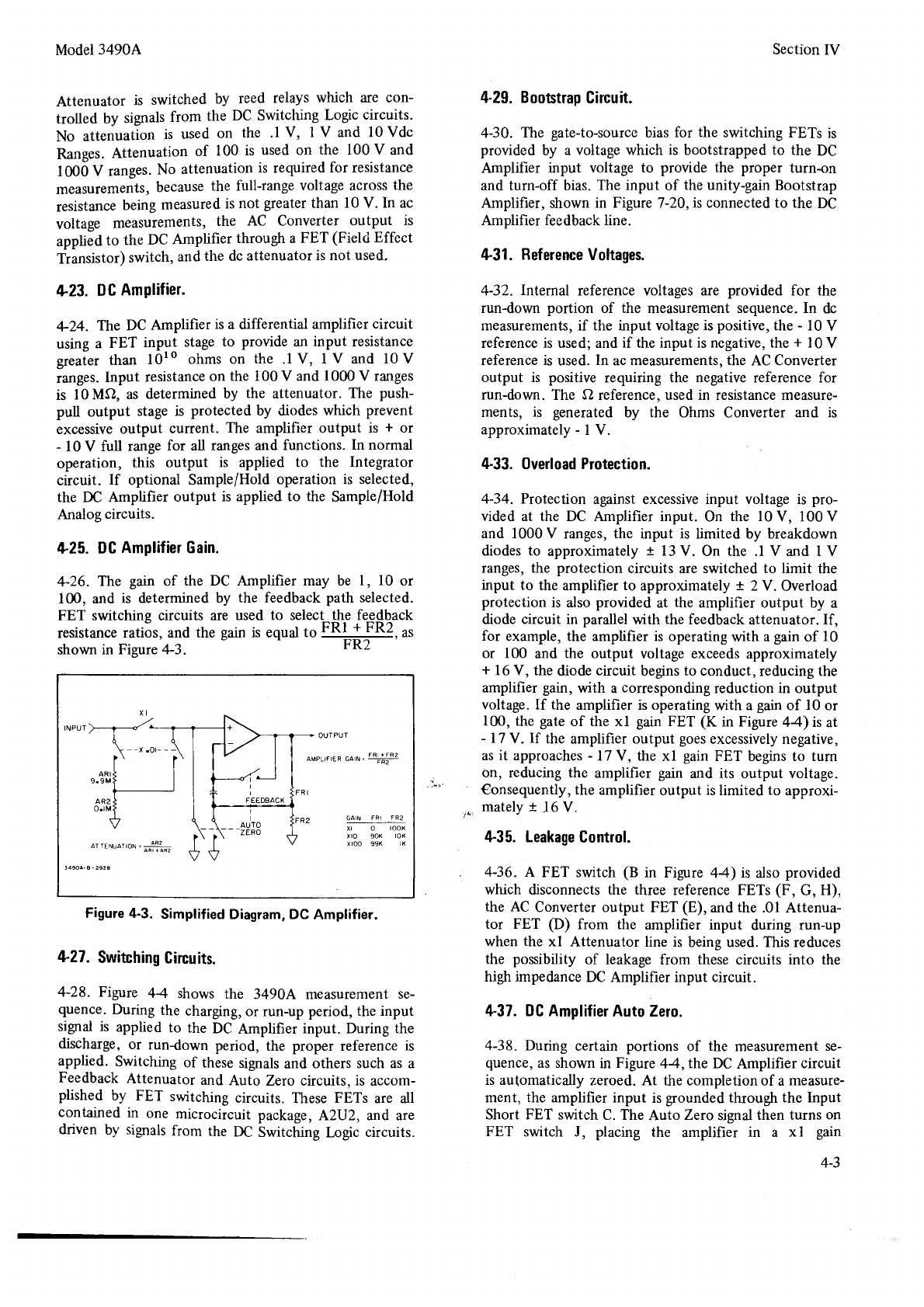
Model
34904
Attenuator is switched by reed relays which are con-
trolled by signals
from the DC Switching Logic circuits'
No attenuation is used on the .l V, I V and 10 Vdc
Ranges.
Attenuation of 100 is used on the 100 V and
100Ö
V ranges.
No attenuation
is required
for resistance
measurements,
because
the full-range
voltage across
the
resistance
being
measured
is
not greater
than l0 V. In ac
voltage measurements,
the AC Converter output is
applied
to the DC Amplifier through a FET (Field Effect
Transistor)
switch,
and
the dc
attenuator
is not used.
+23.
DC
AmPlifier.
424. The DC Amplifier is a differential amplifier circuit
using
a FET input stage
to provide
an
input resistance
sreater
than l0ro ohms on the .l V, I V and lOV
i*g.r. Input resistance
on the 100
V and 1000 V ranges
is l0MO, as determined
by the attenuator.
The push-
pull output stage is protected by diodes which prevent
excessive
output current. The amplifier output is f or
- 10 V full range
for aU ranges and functions. In normal
operation, this output is applied to the Integrator
circuit. If optional Sample/Hold
operation is selected,
the DC Amplifier output is applied to the Sample/Hold
Analog
circuits.
+25.
OC
Amplifier
Gain.
4-26. T\'rc
gain of the DC Amplifier may be l, l0 or
100, and is determined
by the feedback
path selected.
FET switching circuits are used to select the fee{back
resistance
ratios, and the gain
is equal
to FRI-I -FR2,
as
shown
in Figure 4-3. FR2
OUTPUT
ARI
9.9
M
aMPLTFIEF CA]N
- --i-
FRI
AR2
O.IM
aTTENUaTToN, aR2 $$
GA N FRI FR2
xr o roox
xro 90K roK
xroo 99K x
Figure 4-3. Simplified
Diagram, DC
Amplifier.
Section
IV
4-29. Boottrap
Circuit.
4-30. The gate-to-source
bias for the switching FETs
is
provided
by a voltage
which is bootstrapped to the DC
Amplifier input voltage to provide the proper turn-on
and turn-off bias.
The input of the
unity-gain
Bootstrap
Amplifrer,
shown
in Figure
7-20,
is connected to the DC
Amplifier feedback line.
l[.31. Reference
Voltages.
4-32. lnternal reference voltages are provided for the
run-down portion of the measurement
sequence. In dc
measurements, if the input voltage is
positive,
the
- l0 V
reference is used; and
if the
input is negative, the + l0 V
reference is used.
In ac measurements,
the AC Converter
output is positive requiring the negative
reference for
run-down. The Sl reference, used in resistance measure-
ments, is generated
by the Ohms Converter and is
approximately
- I V.
4-33. Overload Protection.
4-34. Protecfion
against excessive input voltage is pro-
vided at the DC Amplifier input. On the 10
V, 100 V
and 1000V ranges,
the input is limited by breakdown
diodes to approximately
1 13
V. On the .1 V and I V
ranges, the protection
circuits
are
switched to limit the
input to the amplifier to approximately x 2 V. Overload
protection
is also
provided
at the amplifier output by a
diode circuit in parallel
with the
feedback
attenuator.
If,
for example, the amplifier is operating
with a
gain
of l0
or 100 and the output voltage exceeds
approximately
+ l6 V, the
diode
circuit begins to conduct,
reducing the
amplifier
gain,
with a
corresponding
reduction
in output
voltage. If the amplifier is operating
with a
gain
of l0 or
100, the gate
of the xl gain
FET (K in Figure
44)isar
- 17
Y.If the amplifier output goes
excessively negative,
as
it approaches
- 17 V, the xl gain
FET begins to turn
on, reducing the amplifier gain and its output voltage.
€onsequently, the amplifier
output is
limited to approxi-
mately
1 16
V.
4-35. Leakage
Gontrol.
4-36. A FET switch (B in Figure
44) is also
provided
which disconnects the three reference FETs
(F, G, H),
the AC Converter output FET (E),
and
the .01 Attenua-
tor FET (D) from the amplifier input during run-up
when
the xl Attenuator line is being used. This reduces
the posibility of leakage from these circuits into the
high impedance
DC Amplifier input circuit.
4-37. DC Amplifier
Auto Zero.
4-38. During certain portions of the measurement
se-
quence,
as shown
in Figure
44,lhe DC Amplifier circuit
is automatically
zeroed. At the completion
of a measure-
ment, the amplifier input is
grounded
through
the Input
Short FET switch
C. The
Auto Zero
signal
then turns
on
FET switch J, placing the amplifier in a xl gain
4-27.
Switching
Circuits.
4-28. Figure 4-4 shows the 3490A measurement
se-
quence.
During the charging,
or run-up
period, the input
sigtal is applied to the DC Amplifier input. During the
discharge,
or run{own period, the proper reference
is
applied.
Switching
of these
signals
and
others such as a
Feedback
Attenuator and
Auto Zero circuits.
is accom-
plished by FET switching
circuits.
These
FETs are all
contahed in one microcircuit package,
A2UZ, and are
driven by signals
from the DC Switching Logic circuits.
4-3
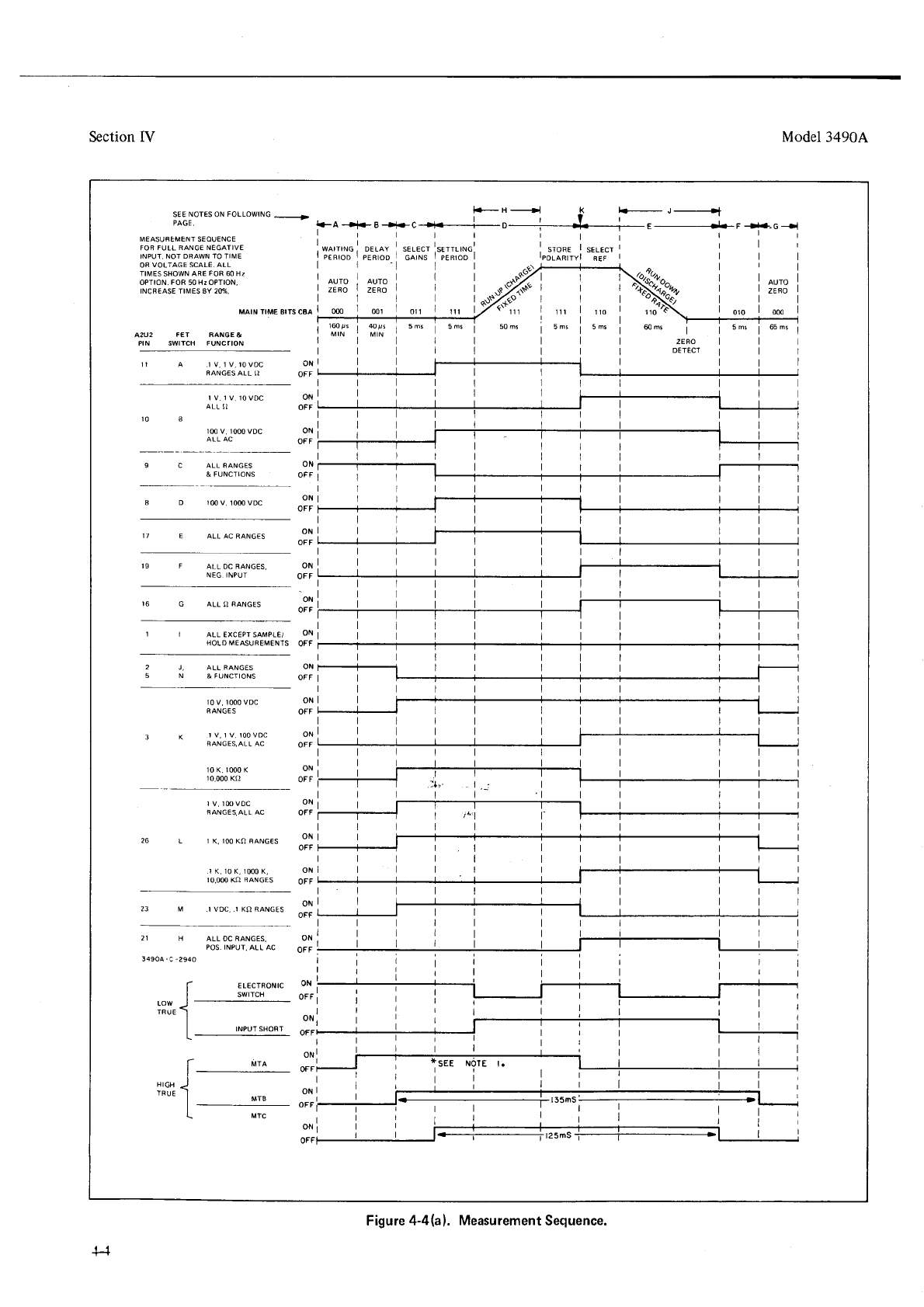
Section
IV Model3490A
sEE NOTES ON FOLLOWTNG .."........-
PAGE.
MEASUFEMENT SEOUENCE
FOR FULL RANGE NEGATIVE
tNPUT.
NOT DRAWN TO TIME
OR
VOLTAGE SCALE. ALL
TIMES SHOWN
ARE FOR 60 Hz
OPTION. FOR 50 Hz OPTION,
INCB€ASE TIM€S BY 2O%,
MAIN TIME BITS
CAA
A2U2 FET RANGE
&
PIN SWITCH FUNCTION
I rP.f' | @!! | sms sms | 50is
, MIN ' MIN '
I to
5ms 5ms 65 ms
rttll
IV,1V,10VDC
ALL
II
1m v. 1000 voc
ON
OFF
ON
OFF
ALL BANGES
& FUNCTIONS
ON
OFF
ON
OFF
ON
OFF
ON
OFF
lm v. 10m vDc
11 ALL AC RANG€S
ALL DC RANGES,
NEG INPUT
ON
OFF
ON
OFF
ALL t} RANGES
ALL ExcEPT sAMPL€/ oN
HOLD MEASUsEMENTS
OFF
ALL RANGES
& FUNCTIONS
ON
OFF
10 v, 1000 vDc
RANGES
r v, r v. !00 vDc
BANGES,ALL AC
10 K. 1m0 K
10.000 Ktl
ON
OFF
ON
OFF
ON
OFF
r v. rm vDc oN
RANG€S,ALL AC OFF
I K. lOO KQ BANG€S
r K.10 K, 1m0 K,
IO,OM KQ
RANGES
ON
OFF
ON
OFF
I VOC..t KQ RANGES ^::
2t H
3490A
-
C
-2940
ALL OC RANGES.
POS. INPUT,
ALL AC
ELECTRONIC
swtTcH
ON
OFF
ON
'-{
"""
J
tt",
I
INPUT SHORT
MTB
l+-H-------l .K ||- J---{
t-a -N.- B
-rt-- c
-++ r -----]---+---]-. ---i* F
--r-. c i
lrrttifilllrrlllrltlrl
ltrl
.
warrrNc, DELAy serecr serrrrncl I srone I srrecr | | | I
lpEgroolpenroolcartslpenrool lporlnttvl
nEr | | | |
| 1 'l I I cr-,1--!----t ^ | | |
,Oü
i :l;s, :y;s
i i '*'{t i-----}...'otu'' i r
, , i^gff*i l i'Xk i itYrs
l1
Figure 4-4(al. Measurement
Sequence.
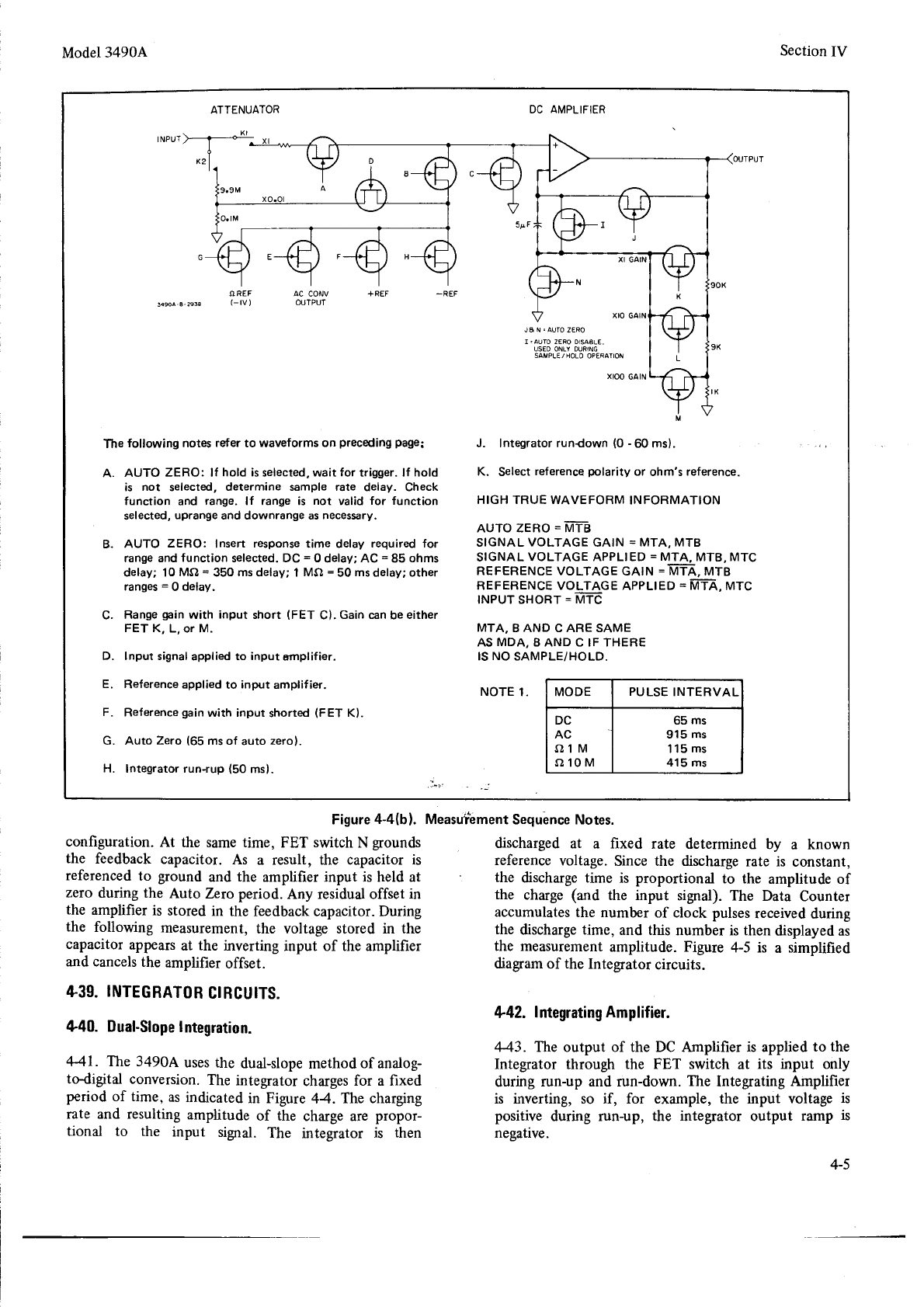
DC AMPLIFIER
ac coNv
OUTPUT
J6N'AUTOZERO
I.AUTO ZERO DISA6L€,
USED ONLY DURING
SAMPL€/ HOLD
OPERAIION
The following notes refer to waveforms on preceding
page:
A. AUTO ZERO: lf hold is
selected, wait for trigger. lf hold
is not selected, determine sample rate delay. Check
function and range. lf range is not valid for function
selected,
uprange
and downrange as
necessary.
8. AUTO ZERO: Insert response
time delay required for
range and function selected. DC = 0 delay; AC = 85 ohms
delay; 10
Mo = 350 ms
delay; 1 MA = 50 ms
delay; other
ranges
= 0 delay.
C. Range
gain
with input short (FET Cl. Gain can
be
either
FET K, L, or M.
D. Input signal
applied
to input amplifier.
E. Reference applied to input amplif ier.
F. Reference
gein
with input shorted
(FET K).
G. Auto Zero (65
ms of auto zero).
H. Integrator run-rup (50 ms).
NOTE 1.
J. Integrator rundown
(0
-
60 ms).
K. Select
reference
polarity
or ohm's
reference.
HIGH TRUE WAVEFORM
INFORMATION
AUTO ZERO
=MT-B
SIGNAL
VOLTAGE
GAIN
=
MTA, MTB
SIGNAL
VOLTAGE APPLIED
=
MTA. MTB, MTC
REFERENCE
VOLTAGE GAIN
=MTA,
MTB
REFERENCE VOLTAGE
APPLIED
=
ili=iÄ, TUTC
INPUT SHORT
=
MTC-
MTA,
B AND C ARE SAME
AS
MDA,
B AND C IF THERE
IS
NO
SAMPLE/HOLD.
MODE PULSE
INTERVAL
DC
AC
ol M
s,10 M
65
ms
915
ms
115
ms
415 ms
Figure
4-4(b). Measuibment
Sequence Notes.
Model
34904
configuration. At the same time, FET switch N grounds
the feedback capacitor. As a result, the capacitor is
referenced to ground and the amplifier input is held at
zero during the Auto Zero period. Any residual offset in
the amplifier is stored in the feedback capacitor. During
the following measurement,
the voltage stored in the
capacitor appears
at the inverting input of the amplifier
and cancels
the amplifier offset.
4.39.
INTEGRATOR
CIRCUITS.
440. Dual-Slope
Integration.
4-41. The 34904 uses the dual,slope
method
of analog-
todigital conversion.
The integrator charges
for a fixed
period of time, as indicated in Figure 44. The charging
rate and resulting
amplitude
of the charge are propor-
tional to the input signal. The integrator is then
discharged at a fixed rate determined by a known
reference
voltage.
Since the discharge
rate is constant,
the discharge time is proportional to the amplitude of
the charge (and the input signal). The Data Counter
accumulates
the number
of clock pulses
received
during
the discharge time, and this number is then displayed
as
the measurement
amplitude. Figure 4-5 is a simplilied
diagram
of the Integrator circuits.
442. Integrating
Amplifier.
443. Tl're output of the DC Amplifier is applied to the
Integrator through the FET switch at its input only
during run-up and run-down. The Integating Amplifier
is inverting, so if, for example, the input voltage is
positive during run-up, the integrator output ramp is
negative.
Section
IV
4-5
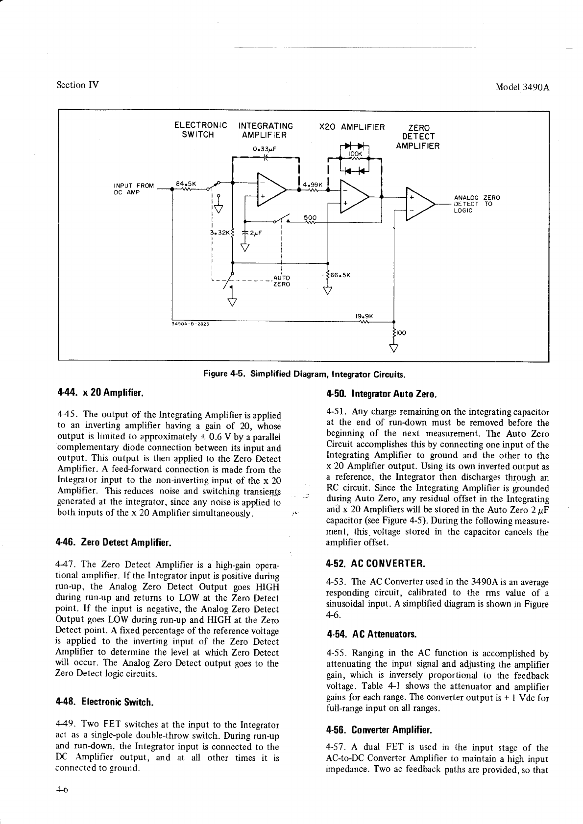
Section
IV Model
3490A
ELECTRONIC
INTEGRATING
SWITCH AMPLIFIER XzO AMPLIFIER ZERO
DETECT
AMPLIFIER
INPUT
FROM
OC AMP ANALOG
DETECT
LOG
IC
ZERO
TO
Figure 4-5. Simplified
Diagram, Integrator
Circuits.
L44. x
20
Amplifier.
445. The output of the Integrating
Amplifier
is applied
to an inverting amplifier having a gain of 20, whose
output is limited to approximately t 0.6 V by a
parallel
complementary
diode connection
between its input and
output. This output is then applied to the Zerc Detect
Amplifier. A feed-forward
connection is made
from the
Integrator
input to the non-inverting
input of the x 20
Atnplifier. This
reduces noise and switching transieq{s
generated
at the integrator,
since
any noise is
applied to
both inputs
of the x 20 Amplifier simultaneously. n
446. Zerc
Detect Amplifier.
447 . The Zero Detect Amplifier is a high-gain opera-
tional amplifier.
If the
Integrator
input is positive
during
run-up, the Analog Zero Detect Output goes HIGH
during run-up and returns to LOW at the Zero Detect
point. If the input is negative, the Analog
Zero DeLect
Output goes
LOW during run-up
and HIGH at the Zero
Detect
point. A frxed
percentage
of the
reference
voltage
is applied to the inverting input of the Zero Detect
Amplifier to determine the level at which Zero Detect
will occur. The Analog
ZeroDetect output goes
to the
Zero
Detect
logic
circuits.
448. Electronic
Switch.
4-49. Two FET switches
at the input to the Integrator
act as a sinele-pole
double-throw
switch.
During
run-up
and rundown. the Integrator
input is connected
to the
DC .tmplit-rer output, and at all other times it is
coflreu-tcd to ground.
J-tt
450. Integrator
Auto Zero.
4-51. Any charge
remaining on the integating capacitor
at the end of rundown must be removed before the
beginning
of the next measurement.
The Auto Zero
Circuit accomplishes
this by connecting
one input of the
Integrating
Amplifier to ground and the other to the
x 20 Amplifier output. Using its own inverted
output as
a reference, the Integator then discharges through an
RC circuit. Since the Integrating Amplifier is gounded
during Auto Zero, wry residual offset in the Integrating
and
x 20 Amplifiers will be stored in the Auto Zero 2 pF
capacitor
(see
Figure 4-5).
During
the following
measure-
ment, this.voltage stored in the capacitor
cancels
the
amplifier offset.
4.52. AC CONVEBTEB.
z1-53.
The AC Converter used
in the 3490A
is an average
responding
circuit, calibrated to the rms value of a
sinusoidal input. A simplified diagram
is shown
in Figure
4-6.
4-54. AC Attenuators.
4-55. Ranging
in the AC function is accomplished
by
attenuating the input sigral
and
adjusting
the amplifier
gain, which is inversely proportional to the feedback
voltage.
Table 4-1 shows the attenuator
and amplifier
gains
for each
range. The converter
output is
+ I Vdc for
full-range
input on all ranges.
4-56. Converter
Amplifier.
4-57. A dual FET is used in the input stage
of the
AC-to-DC Converter Amplifier to maintain
a high input
impedance. Two ac feedback paths
are
provided,
so that
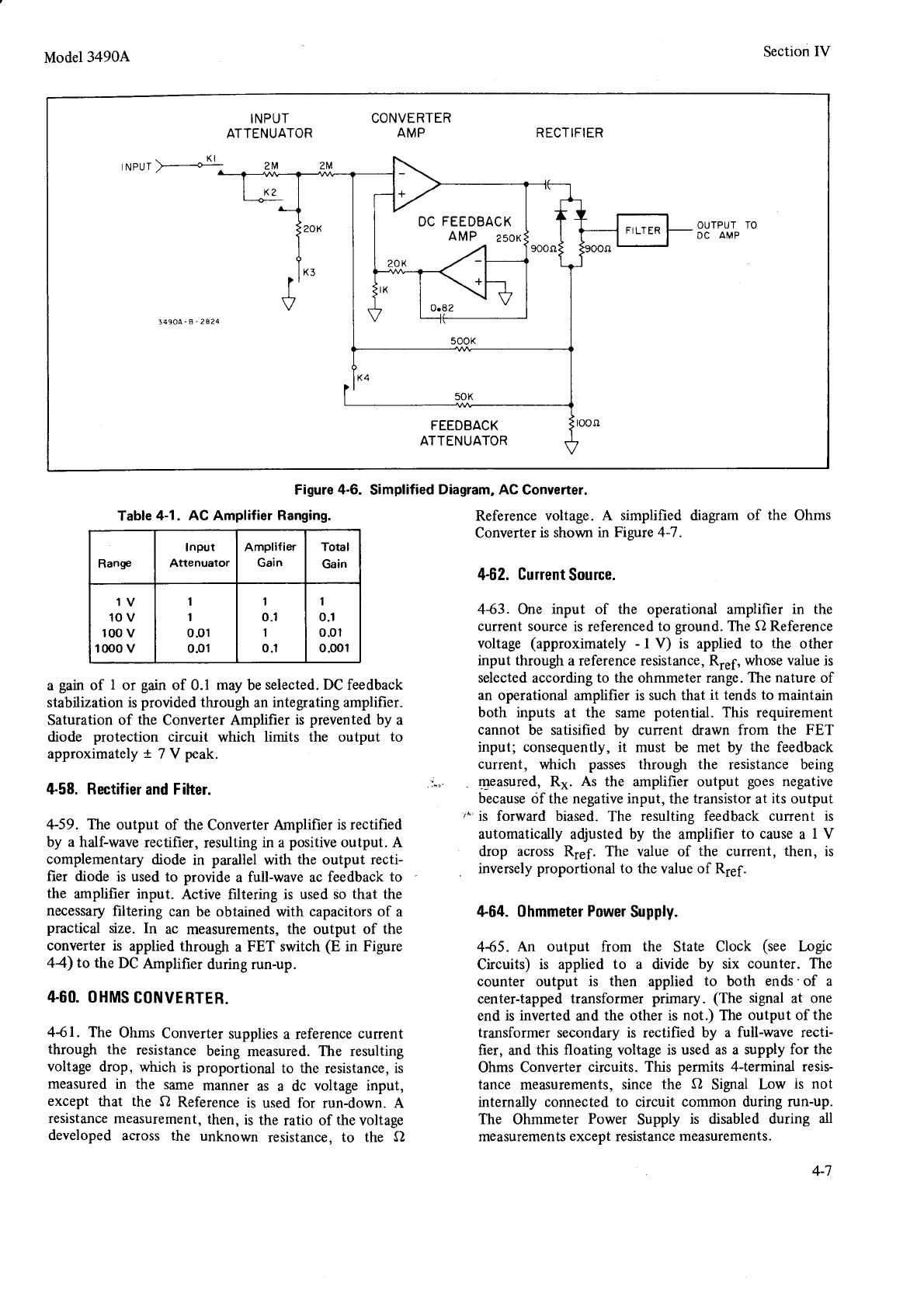
INPUT
ATTENUATOR CONVERTER
AMP RECTIFIER
rNeur{ ?M
K?
OUTPUT
DC AMP
3490A-A-2824
50K
FEEDBACK
ATTENUATOR
DC
FEEDBACK
AMP 25oK FI
LTER
Model
34904
Figure
4-6.
Table
4-1. AC Amplifier
Ranging.
Range
I
nput
Attenuator
Amplifier
Gain
Total
Gain
1V
10v
1(X)
v
1000 v
1
1
0.o1
0.01
1
o.1
1
0.1
1
0.1
0.01
o.001
a gain
of I or gain
of 0.1 may be
selected. DC
feedback
stabilization is provided through an integating amplifier.
Saturation of the Converter Amplifier is prevented
by a
diode protection circuit which limits the output to
approximately
1 7 V peak.
&58. Rectifier
and Filter.
zt-59. The output of the Converter
Amplifier is rectified
by a half-wave
rectiher, resulting
in a positive
output. A
complementary diode in parallel with the output recti-
fier diode is used to provide a full-wave ac feedback to
the amplifier input. Active filtering is used so that the
necessary
filtering can be obtained with capacitors of a
practical size. In ac measurements, the output of the
converter is applied through a FET switch (E in Figure
44) Io the DC Amplifier during run-up.
4.60.
OHMS
CONVERTER.
461. The Ohms Converter
supplies
a reference
current
through the resistance
being measured.
The resulting
voltage
drop, which is proportional
to the resistance,
is
measured
in the same
manner as a dc voltage input,
except that the Q Reference
is used for run-down. A
resistance measurement,
then,
is the ratio of the
voltage
developed across the unknown resistance, to the Q
Section
IV
Simplified
Diagram, AC Conyerter.
Reference voltage.
A simplified diagam of the Ohms
Converter
is shown in Fizure 4-7.
4-62.
Current
Source.
443. One input of the operational amplifier in the
current source
is referenced
to ground.
The
,fl
Reference
voltage (approximately - I V) is applied to the other
input through a reference resistance, Rr.1, whose
value
is
selected
according
to the ohmmeter range. The
nature
of
an operational amplifier is such that it tends to maintain
both inputs at the same potential. This requirement
cannot be satisified by cunent drawn from the FET
input; consequently,
it must be met by the feedback
current, which passes
through the resistance being
- measured, R1. As the amplifier output goes
negative
because df the negative input, the
transistor
at its output
'"'
is forward biased.
The resulting feedback current is
automatically adjusted by the amplifier to cause
a I V
drop across R.e;. The value of the current, then, is
inversely
proportional
to the
value
of R1s1.
464. 0hmmeter
Power
Supply.
4-65. An output from the State Clock (see Logic
Circuits) is applied to a divide by six counter. The
counter output is then applied to both ends'of a
center-tapped
transformer primary. (The signal at one
end
is inverted
and the other is not.) The output of the
transformer secondary is rectified by a full-wave recti-
fier, and this floating voltage
is used as a supply for the
Ohms
Converter circuits.
This permits 4-terminal resis-
tance measurements,
since the A Sipal Low is not
internally connected to circuit common during run-up.
The Ohmmeter Power Supply is disabled during all
measurements except resistance
measurements.
+7
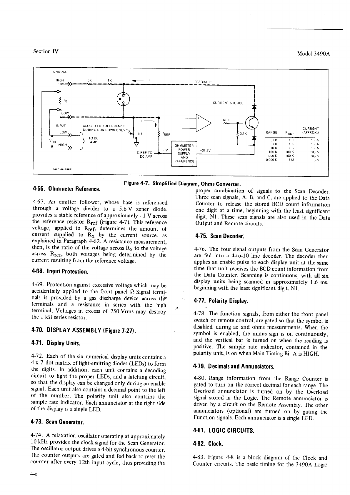
Section IV
466.
0hmmeter
Reference. Figure
4-7. Simplified
Model 3490A
Diagram,
Ohms
Converter.
proper combination of signals
to the Scan Decoder.
Three
scan
signals,
A, B, and
C, are applied
to the Data
Counter to release
the stored
BCD count information
one digit at a time, beginning
with the least
significant
digit, Nl. These
scan
signals
are also used in the Data
Output
and Remote
circuits.
4-75.
Scan Decoder.
4-16. The four signal
outputs
from the Scan Generator
are fed into a 4-to-10 line decoder. The decoder
then
applies
an enable
pulse
to each
display unit at the same
time that unit receives
the BCD
count
information
from
the Data Counter.
Scanning is continuous,
with all six
display
units being scanned
in approximately
1.6 ms,
beginning
with the least significant
digit,
Nl.
4-78. The function signals,
from either
the front panel
switch
or remote control,
are
gated
so
that the symbol
is
disabled
during ac and ohms
measurements.
When
the
symbol is enabled,
the minus sign
is on continuously,
and the vertical bar is turned on when the reading
is
positive. The sample
rate indicator, contained
in the
polarity
unit, is on when Main Timing
Bit A is HIGH.
4-79.
Decimals
and
Annunciators.
4{0. Range information from the Range
Counter is
gated
to turn on the
correct
decimal
for each
range.
The
Overload
annunciator is turned on by the Overload
signal
stored
in the Logic. The Remote
annunciator
is
driven
by a circuit on the Remote
Assembly.
The
other
annunciators (optional) are turned on by gating the
Function
signals. Each
annunciator
is
a single
LED.
4.81.
L0GrC
C|RCU|TS.
4-82.
Clock.
4-83. Figure 4-8 is a block diagram
of the Clock and
Counter
circuits.
The basic timing for the 3490A Ilgic
+67 . An emitter follower, whose base is referenced
through a voltage divider to a 5.6
V zener diode.
provides
a stable
reference
of approximately
- I V across
the reference resistor Rrs6 (Figure 4-7). This reference
voltage, applied to Rpsg,
determines
the amount of
current supplied to R1 by the current source, as
explained
in Paragraph
442. A resistance
measuremenr,
then,
is the ratio of the voltage
across
R* to the
voltage
across R1s;, both voltages
being determined by the
current
resulting
from the
reference
voltage.
468. Input
Protection.
4-69. Protection
against
excessive
voltage
which
may
be
accidentally
applied
to the front panel
Q Signal
termi-
nals is provided by a gas
discharge
device
across th:ä
terminals and a resistance
in series with the hieh
terminal. Voltages
in excess of 250 Vrms may deströy
the I kfl series
resistor.
+70.
0ISPLAY
ASSEMBLY
(Figure
7-2?).
471.
Display
Units.
4-72. Each
of the six numerical
display units
contains
a
4 x 7 dot
matrix of light-emitting
diodes
(LED$ to form
the digits. In addition, each
unit contains
a decoding
circuit to light the proper
LEDs,
and
a latching
circuit,
so
that the display
can
be changed
only during
an enable
signal.
Each
unit also
contains
a
decimal point to the left
of the number. The polarity unit also contains the
sample
rate indicator.
Each
annunciator
at the right side
of the display
is
a single
LED.
473.
Scan
Generator.
+74. A relaxation
oscillator
operating
at approximately
l0 kHz provides
the
clock
signal
for the Scan
Generator.
The
oscillator
output drives
a 4-bit
synchronous
counter.
The
counter outputs
are
gated
and
fed back
to reset the
counter
after every
I 2th input cycle, thus
providing
the
-1-ö
FEE D BACK
OURING
RUN.DOWN
ONLY
I ,oo.
/ rnre
)
'J
K1
II
V
O
REF TO
DC AMP
CURRENT
RRer 1APPROX l
,I
K I K
1K IK
10 K I K
100 K 100 K
1.000 K 100
K
10.000 K 1 lvl
l0
!A
l0
!A
CURBENT
SOURCE
6.8K
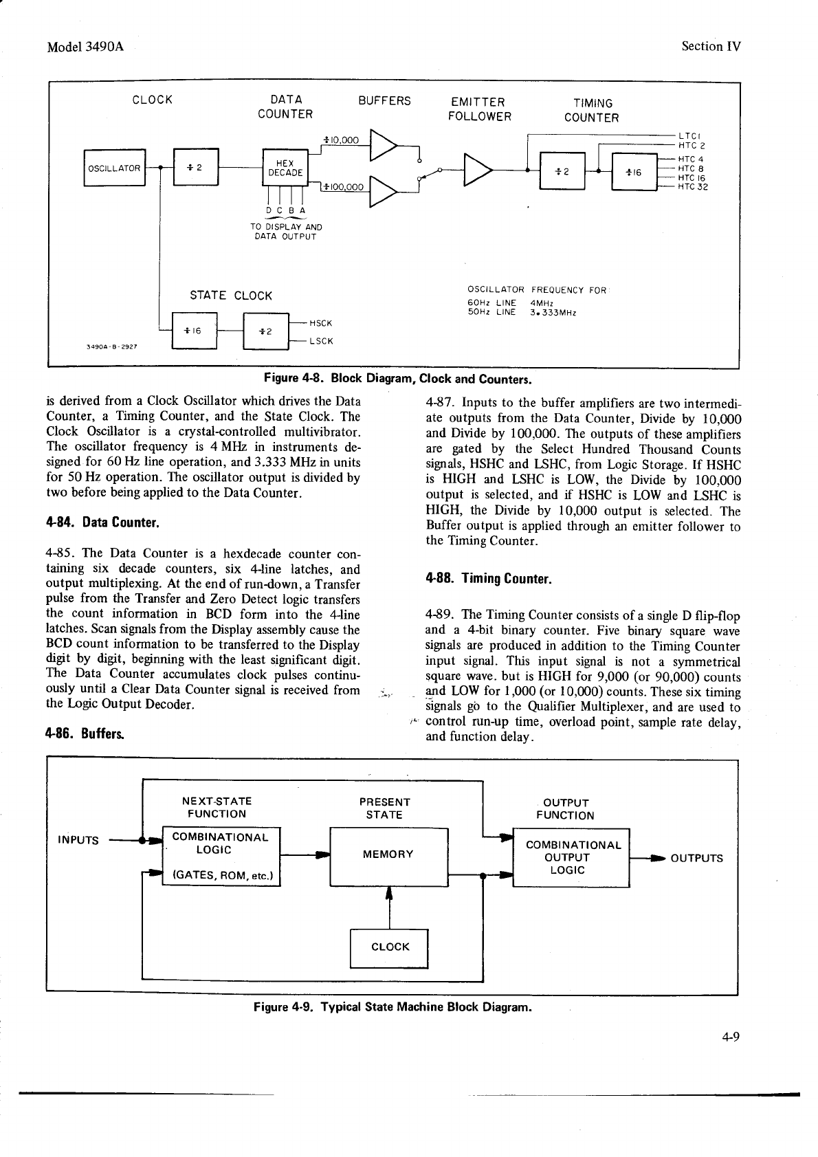
Model3490A Section
IV
CLOCK DATA
COUNTER BUFFERS EMITTER
FOLLOWER TIMING
COUNTER
LTC
I
HJC 2
HTC
4
HTC
8
HTC
16
HTC
32
DCBA
TO
DISPLAY
AND
DATA
OUIPUT
STATE
CLOCK OSCILLATOR
FREOUENCY
6OHz LINE 4MHz
50Hz LINE 3.333MH2
FOR
Figure 4-8. Block Diagram,
Clock
and
Counters.
is derived from a Clock Oscillator which drives
the Data
Counter, a Timing Counter, and the State Clock. The
Clock Oscillator is a crystal-controlled multivibrator.
The oscillator frequency is 4 MtIz in instruments de-
signed for 60 Hz line operation,
and 3.333
MHz in units
for 50 Hz operation. The oscillator output is divided by
two before being applied to the Data
Counter.
484. Data Gounter.
4{5. The Data Counter is a hexdecade
counter con-
taining six decade counters, six 4line latches,
and
output multiplexing. At the end of rundown, a Transfer
pulse from the Transfer and Zero Detect logic transfers
the count information in BCD form into the 4-line
latches.
Scan signals
from the Dsplay assembly cause the
BCD count information to be transferred
to the Display
digit by digit, beginning
with the least significant digit.
The Data Counter accumulates
clock pulses continu-
ously until a Clear
Data Counter signal
is received from
the logic Output Decoder.
486. Buffers
4€7. Inputs to the buffer amplifiers
are
two intermedi-
ate outputs from the Data Counter, Divide by 10,000
and Divide
by 100,000.
The
outputs of these
amplifiers
are gated by the Select Hundred Thousand Counts
signals, HSHC
and LSHC, from Logic Storage.
If HSHC
is HIGH and LSHC is LOW, the Divide by 100,000
output is selected,
and if HSHC is LOW and LSHC is
HIGH, the Divide by 10,000 output is selected.
The
Buffer output is applied
through
an emitter follower to
the Timing
Counter.
4-88. Timing
Counter.
4{9. The Timing
Counter consists
of a
single
D flip-flop
and a 4-bit binary counter. Five binary square wave
sigrals are produced in addition to the Timing Counter
input signal. This input signal is not a symmetrical
$quare
wave. but is HIGH for 9,000 (or 90,000)
counts
and LOW for I ,000
(or 10,000)
counts.
These six timing
signals
gö to the Qualifier
Multiplexer,
and are used to
control run-up time, overload
point, sample
rate delay,
and
function delay.
NEXT.STATE PRESENT
FUNCTION STATE
COMBINATIONAL
LOGIC
(GATES,
RoM,
etc.I
COMBINATIONAL
OUTPUT
LOGIC
INPUTS
OUTPUTS
Figure
4-9. Typical
State
Machine
Block Diagram.
+9
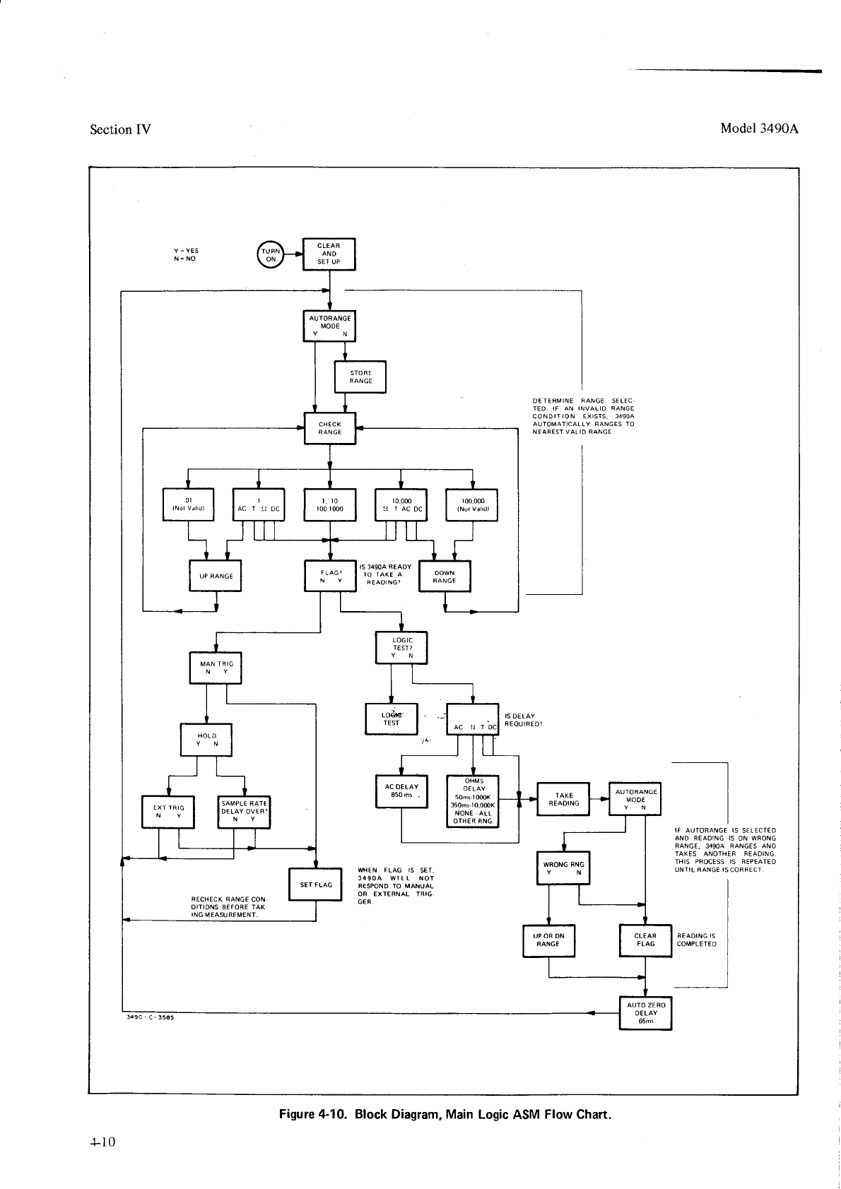
Section
IV Model3490A
Y=YES
N=NO
DEl€AMINE RANGE SELEC.
TED. IF AN INVALID BANGE
CONDITION EXISTS, 34904
AUTOMATICALLY RANGES TO
NEAFEST VALIO RANGE
IS
34904 AEADY
TO TAKE A
R
EADI
NG'
IS
DELAY
REOUIRED)
IF AUIORANC€ IS SEL€CT€O
ANO REAOING IS ON WRONG
RANGE,349OA BANG€S ANO
TAKES ANOTHEF READING.
THIS PROCESS IS REPEATED
UNTIL RANGE IS
CORsECT
R€ADING IS
COMPLET€D
r0,0m
!I IACDC
SEN FLAG IS SET
34904 WILL NOI
B€SPOND TO MANUAL
OR EXTERNAL TRIG
6ER.
BECHECK NANGE CON
OITIONS SEFORE TAK
ING
MEASUREMENT.
y9c'c-35a5
+10
Figure
4-10. Block
Diagram, Main
Logic ASM Flow Chart.
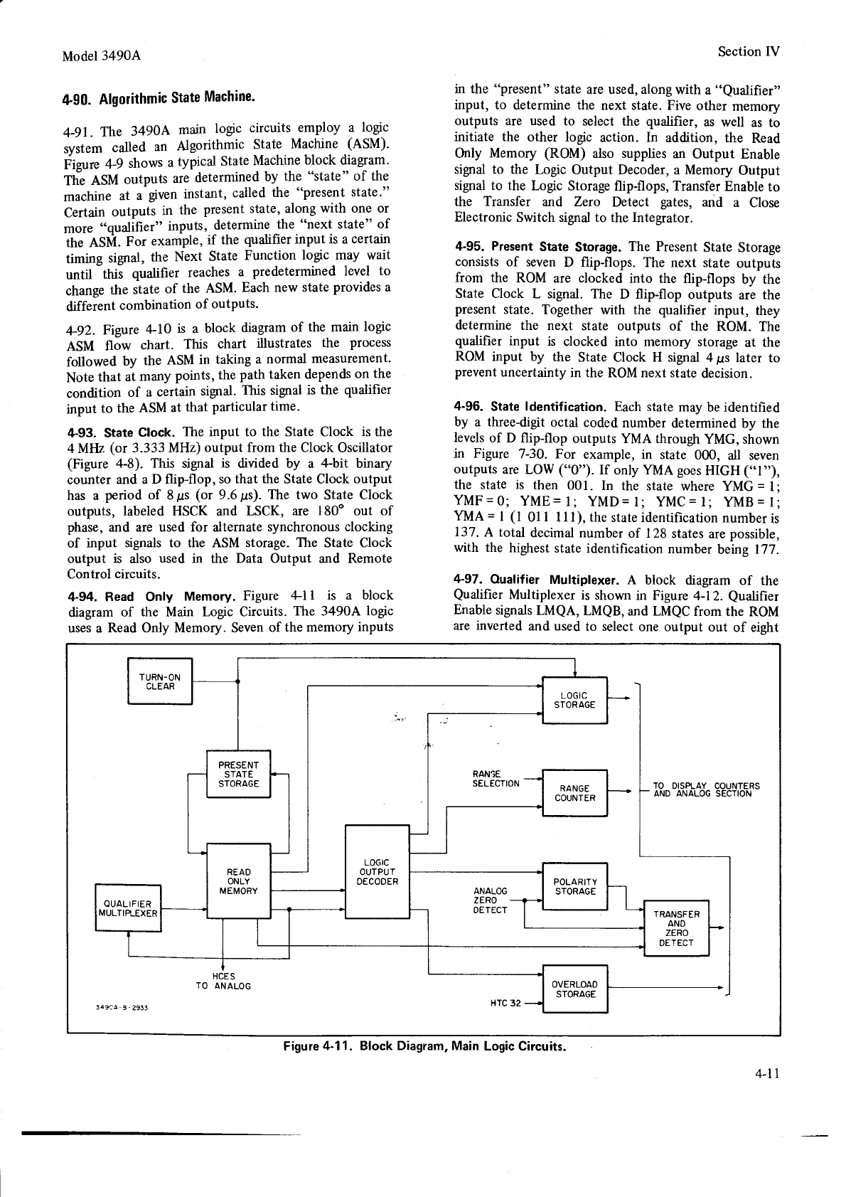
Model3490A
tl-90.
Algorithmic
State
Machine.
4-91.
T\e 3490A main logic circuits employ a logic
svstem called an Algorithmic State Machine (ASM)'
Fizure 4-9 shows
a typical State
Machine
block diagram'
nir nSU outputs are determined
by the "state" of the
machine at a given
instant,
called
the "present
state'"
Certain outputs in the present
state, along with one or
more "qualifier" inputs, determine
the "next state" of
the ASIr{. For example,
if the qualifier input is a certain
timing signal, the Next State Function logic may wait
until this qualifier reaches a predetermined level to
change
the state of the ASM. Each new state
provides
a
different combination of outputs.
492. Figore 4-10 is a block diagram
of the main logic
ASM flow chart. This chart illustrates the process
followed by the ASM in taking a normal measurement'
Note that at many points, the path taken depends
on the
condition of a certain signal.
This signal
is the qualifier
input to the ASM at that particular time.
4-93. State Clock. The input to the State Clock is the
4MlIz (or 3.333 MHz) output from the
Clock Oscillator
(Figure 4-8). This signal is divided by a 4-bit binary
counter and a D flip-flop, so
that the State Clock output
has a period of 8
prs
(or 9.6
ps). The two State Clock
outputs, labeled HSCK and LSCK, are 180" out of
phase, and are used for alternate synchronous clocking
of input signals to the ASM storage. The State Clock
output is also used in the Data Output and Remote
Control
circuits.
4-94. Read Only Memory. Figure +11 is a block
diagram of the Main Ingic Circuits. The 3490A logic
uses a Read Only Memory. Seven
of the memory inputs
Section IV
in the "present"
state
are used, along
with a "Qualifier',
input, to determine the next state. Five other memory
outputs are used to select the qualifier, as well as to
initiate the other logic action. In addition, the Read
Only Memory (ROM) also supplies
an Output Enable
sipal to the Logic Output Decoder,
a Memory Output
sigrral
to the Logic Storage flip-flops, Transfer
Enable
to
the Transfer utd Zero Detect gates, and a Close
Electronic Switch signal to the Integrator.
4-95. Present
State Storage. The Present
State Storage
consists
of seven D flip-flops. The next state outputs
from the ROM are clocked into the flip-flops by the
State Clock L signal. The D flip-flop outputs are the
present state. Together with the qualifier input, they
determine
the next state outputs of the ROM. The
qualifier input is clocked into memory storage at the
ROM input by the State Clock H signal 4 ps later to
prevent
uncertainty
in the ROM next state
decision.
4-96. State
ldentification. Each state
may
be identified
by a three-digit
octal coded
number
determined
by the
levels
of D flip-flop outputs YMA through
YMG, shown
in Figure 7-30. For example,
in state 000, all seven
outputs
are LOW ("0"). If only YMA goes
HIGH ("1"),
the state
is then 001. In the state
where YMG= l;
YMF=0; YME=l; YMD=1; YMC=l; YMB=l;
YMA = I (l 0l 1 I l1), the
state identihcation
number
is
131
. A total decimal number
of 128
states
are
possible,
with the highest
state
identification
number
being 177-
4-97. Oualifier Multiplexer. A block diagram of the
Qualifier Multiplexer is shown in Figure 4-1
2. Qualifier
Enable
signals
LMQA, LMQS, and LMQC from the ROM
are inverted
and used
to select
one output out of eight
Figure
4-1
1. Block Diagram, Main
Logic Circuits.
4-l r
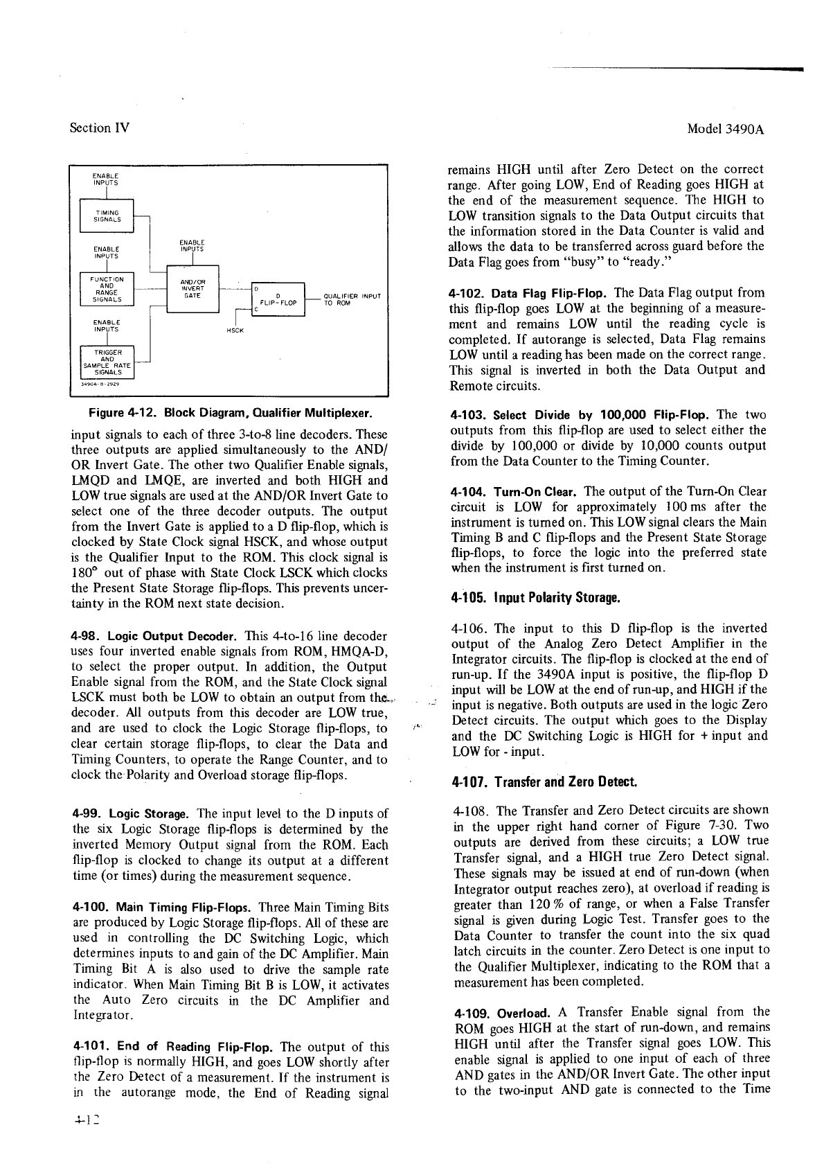
Section IV
ENAELE
I
NPUTS
OUALIFIER
INPUT
TO ROM
ENABLE
Figure
4-12. Block
Diagram, Qualifier Multiplexer.
input signals
to each of three 3-to-8
line decoders.
These
three outputs are applied simultaneously to the AND/
OR Invert Gate. The other two Qualifier
Enable sigrals,
I-il,IQD and LMQE, are inverted and both HIGH and
LOW
true signals
are
used
at the AND/OR Invert
Gate
to
select
one of the three decoder outputs. The output
from the Invert Gate is applied
to a D flip-flop, which is
clocked by State Clock signal HSCK, and whose
output
is the Qualifier Input to the ROM. This clock signal is
180" out of phase
with State Clock LSCKwhich clocks
the Present State Storage
flip-flops. This prevents
uncer-
tainty in the ROM next state
decision.
4-98. Logic Output Decoder.
This
4-to-l6line decoder
uses
four inverted
enable signals
from ROM, HMQA-D,
to select the proper output. In addition, the Output
Enable signal
from the ROM, and the State
Clock signal
LSCK must both be LOW to obtain an
output from the."
decoder. All outputs from this decoder are LOW true,
and are used to clock the Logic Storage
flip-flops, to
clear certain storage flip-flops, to clear the Data and
Timing Counters, to operate the Range Counter, and
to
clock the'Polarity
and Overload storage flip-flops.
4-99. Logic
Storage.
The input level to the D inputs
of
the six Logic Storage flip-flops is determined by the
inverted Memory Output signal from the ROM. Each
flip-flop is clocked to change its output at a different
time (or times)
during
the measurement sequence.
4-100. Main Timing
Flip-Flops.
Three Main
Timing
Bits
are
produced
by Logic
Storage
flip-flops. All of these
are
used in controlling the DC Switching Logic, which
determines inputs
to and
gain
of the
DC Amplifier.
Main
Timing Bit A is also used to drive the sample rate
indicator. When
Main Timing
Bit B is LOW,
it activates
the Auto Zero circuits in the DC Amplifier and
Integrator.
tl-101. End of Reading
Flip-Flop. The output of this
tlip-t1op
is normally
HIGH, and
goes
LOW shortly after
the Zero Detect
of a measurement.
If the instrument is
Ln the autorange
mode, the End of Reading sigral
Model
3490A
remains
HIGH until after Zerc Detect on the correct
range. After going
LOW,
End of Reading
goes
HIGH at
the end of the measurement
sequence.
The HIGH to
LOW transition signals
to the Data Output circuits that
the information stored
in the Data Counter
is valid and
allows
the data
to be
transferred across
guard
before the
Data
Flag
goes
from "busy' to "ready."
4-1O2. Data Flag
Flip-Flop. The Data
Flag output from
this flip-flop goes LOW at the beginning of a measure-
ment and remains LOW until the reading cycle is
completed.
If autorange
is selected, Data Flag remains
LOW
until a reading
has been
made on the correct range.
This signal is inverted in both the Data Output and
Remote circuits.
4-103. Select Divide by 100,000 Flip-Flop. The two
outputs from this flip-flop are
used to select
either the
divide by 100,000 or divide
by 10,000 counts output
from the Data Counter
to the Timing Counter.
4-104. Turn-On
Clear.
The output of the Turn-On Clear
circuit is LOW for approximately 100 ms after the
instrument is tumed on. This LOW
signal clears the Main
Timing B and C flipflops and the Present
State Storage
flip-flops, to force the logic into the preferred state
when the instrument is first turned on.
4-105.
Input Polarity
Storage.
4-106. The input to this D flip-flop is the inverted
output of the Analog Zero Detect Amplifier in the
lntegrator
circuits.
The flip-flop is clocked at the end of
run-up.
If the 34904 input is positive,
the flip-flop D
input will be LOW at the end of run-up, and
HIGH if the
input is
negative. Both outputs are used
in the logic Zero
Detect circuits. The output which goes
to the Display
and the DC Switching LoSc is HIGH for + input and
LOW for - input.
4-107. Transfer and
Zero
Detect.
4108. The Transfer
and
Zerc Detect
circuits are
shown
in the upper right hand corner of Figure 7-30. Two
outputs are derived from these circuits; a LOW true
Transfer
signal,
and a HIGH trve Zerc Detect sigtal.
These signals
may be issued at end of run-down (when
Integrator output reaches
zerc), at overload
if reading
is
greater than 120
% of nnge, or when a False
Transfer
signal is given during Logic Test. Transfer goes
to the
Data Counter to transfer the count into the six quad
latch circuits
in the countet.Zero
Detect
is one
input to
the Qualifier
Multiplexer,
indicating
to the ROM that a
measurement
has
been
comPleted.
4-109. Overload.
A Transfer Enable signal from the
ROM goes
HIGH at the start of run-down,
and remains
HIGH until after the Transfer sigral goes LOW. This
enable
signal
is applied
to one input of each of three
AND gates
in the AND/OR Invert Gate.
The other
input
to the two-input AND gate
is connected
to the Time
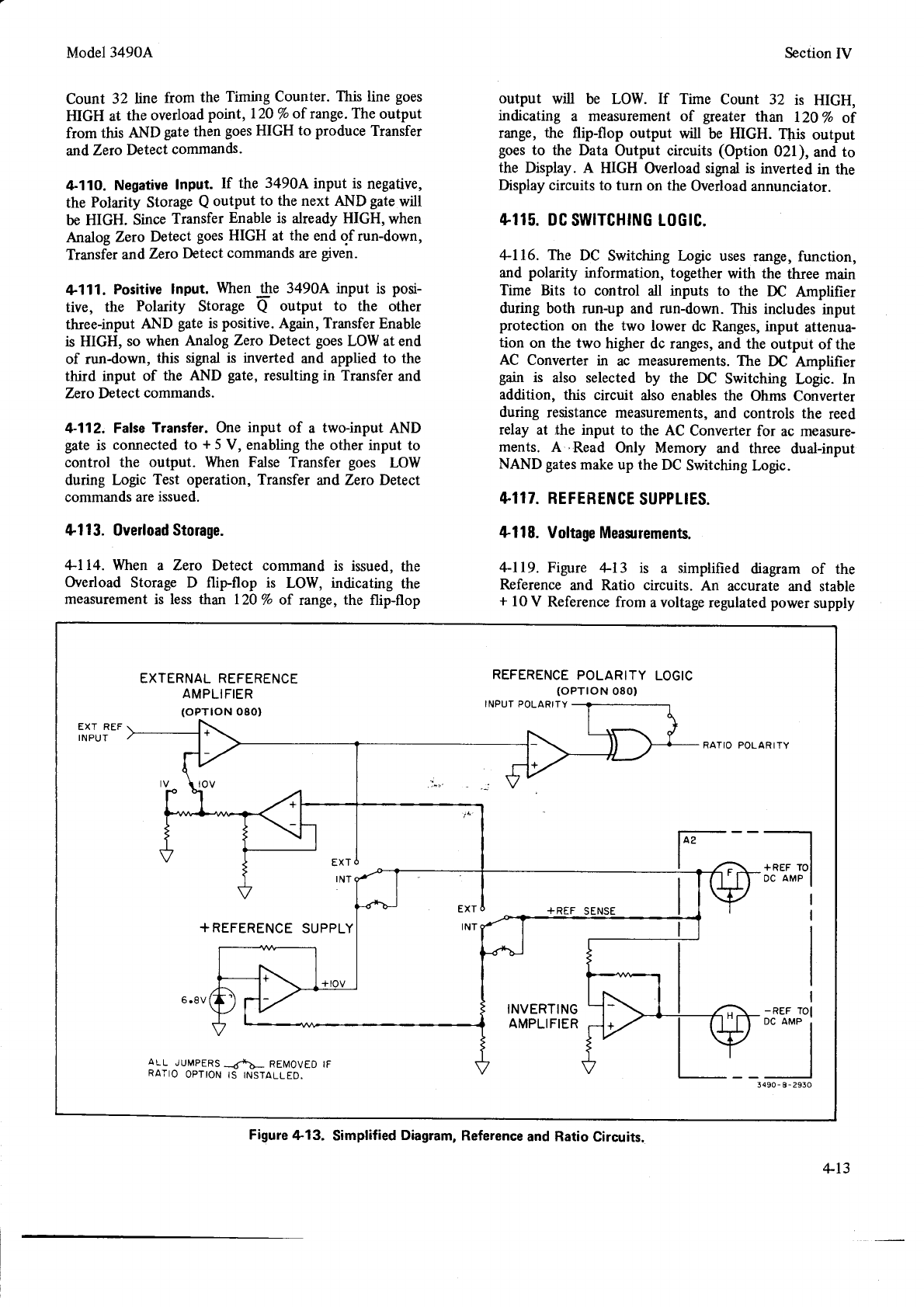
Model3490A
Count 32 line from the Timing Counter. This line goes
HIGH at the overload
point, 120 7o
of runge. The output
from this AND gate
then goes HIGH to produce
Transfer
and
Zero Detect commands.
4-110. Negative
Input. If the 34904 input is negative,
the Polarity Storage
Q output to the next AND gate
will
be HIGH. Since
Transfer
Enable is already HIGH, when
Analog Zerc Detecr goes
HIGH at the end of run-down,
Transfer andZero Detect
commands
are
given.
+111. Positive Input. When Jhe 3490A input is posi-
tive, the Polarity Storage Q output to the other
three-input AND gate
is positive.
Again, Transfer
Enable
is HIGH, so when Analog Zero Detect goes
LOW at end
of rundown, this signal is inverted and applied to the
third input of the AND gate, resulting in Transfer
and
ZercDetect commands.
4-112. False
Transfer. One input of a two-input AND
gate is connected to f 5 V, enabling the other input to
control the output. When False Transfer goes LOW
during Logic Test operation, Transfer and Zero Detect
commands
are
issued.
4113.
Ovedoad
Storage.
+114. When a Zero Detect command is issued,
the
Overload Storage D flipflop is LOW, indicating the
measurement
is less than l2OVo of range, the flip-flop
Section
IV
output will be LOW. If Time Count 32 is HIGH,
indicating a measurement of greater
thm 120
% of
range,
the flip-flop output will be HIGH. T[ris
output
goes
to the Data
Output circuits
(Option
021),
and to
the Display. A HIGH Overload
sigral is inverted
in the
Display
circuits to turn on
the
Overload annunciator.
+il5. DC
SWTTCH|NG LoGrC.
4-1 16. The DC Switching Logc uses range, function,
and polarity information, together with the three main
Time Bits to control all inputs to the DC Amplifier
during both run-up and run-down. This includes input
protection on the two lower dc Ranges, input attenua-
tion on the two higher dc ranges,
and the output ofthe
AC Converter in ac measurements.
The DC Amplifier
gain is also selected by the DC Switching Logic. In
addition, this circuit also enables
the Ohms Converter
during resistance
measurements,
and controls the reed
relay at the input to the AC Converter
for ac measure-
ments. A ,Read Only Memory and three dual-input
NAND gates
make up the DC Switching
Logic.
+II7. REFERENCE
SUPPLIES.
ll.l
18.
Voltage Mea$rements.
4-119. Figure 4-13 is a simplified diagram of the
Reference and Ratio circuits. An accurate and stable
+ l0 V Reference from a voltage
regulated
power supply
EXTERNAL REFERENCE
AMPLIFIER
(oPTloN o80)
REFERENCE
POLARITY
LOGIC
(oPTtoN 080)
INPUT
POLARITY
EXT REF
INPUT RATIO POLARITY
EXT
INT
+REFERENCE
SUPPLY
aLL JUMPERS
_<*-b_ REMovEo
tF
RATIO
OPTION
IS
INSTALLEO. I
,rtl +REF
sENsE I
3490-8-2930
Figure
z1-13.
Simplified
Diagram,
Reference
and Ratio
Circuits.
+13
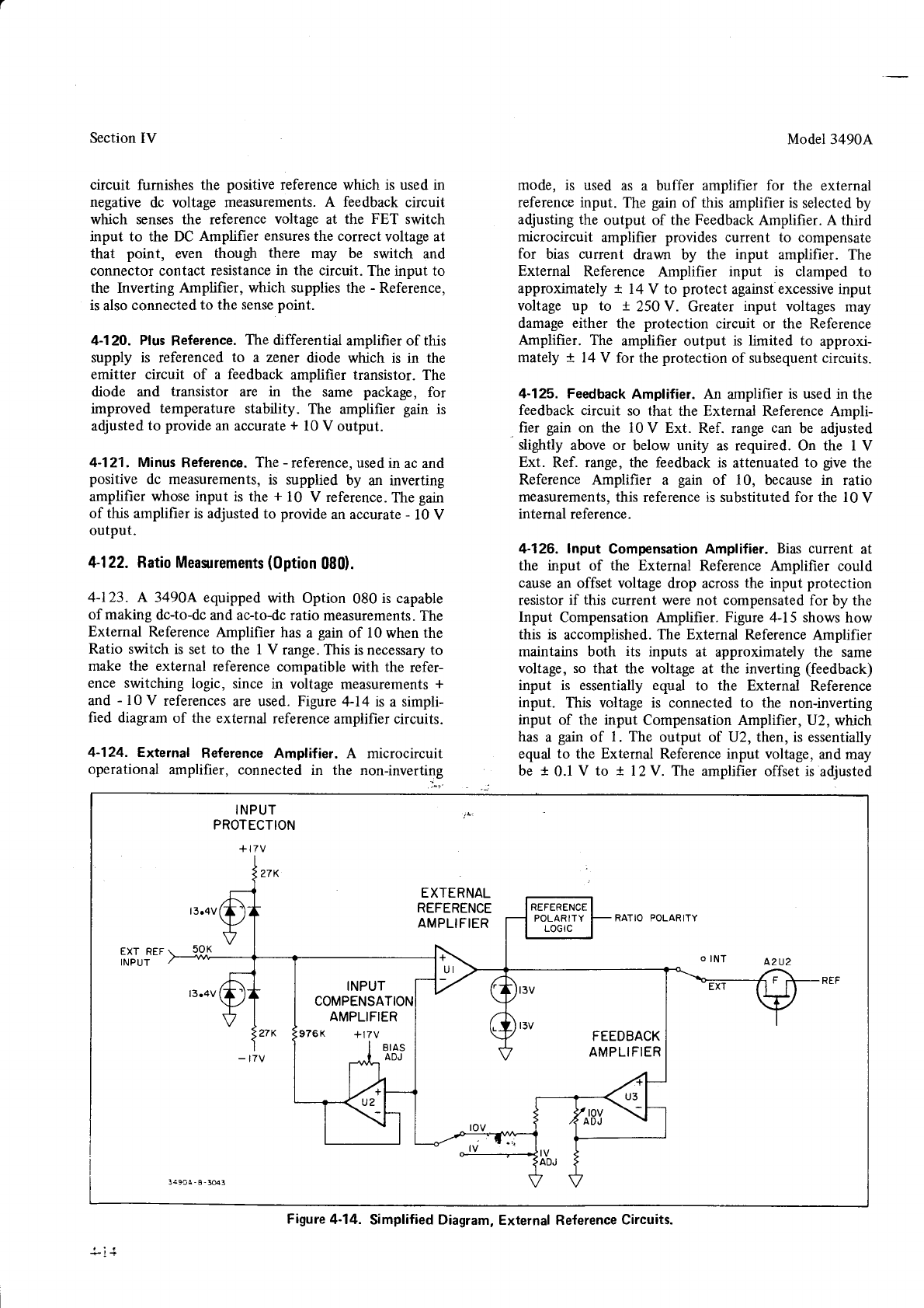
Section
IV
circuit fumishes the positive reference
which is used in
negative dc voltage measurements.
A feedback circuit
which senses the reference voltage at the FET switch
input to the DC Amplifier ensures
the correct
voltage at
that point, even though there may be switch and
connector
contact
resistance
in the circuit.
The input to
the Inverting Amplifier, which supplies the - Reference,
is also connected
to the sense
point.
4-1 20. Plus
Reference.
The
differential
amplifier of this
supply is referenced to a zener diode which is in the
emitter circuit of a feedback amplifier transistor. The
diode and transistor are in the same package, for
improved temperature stability. The amplifier gain is
adjusted
to provide
an accurate
+ l0 V output.
4-1
21. Minus Reference. The
- reference, used
in ac and
positive dc measurements,
is supplied by an inverting
amplifier whose
input is the + 10 V reference.
The gain
of this amplifier is
adjusted to provide
an accurate
- l0 V
output.
4-122. Ratio Measrements
(0ption
080).
4-123. A 34904 equipped
with Option 080 is capable
of making
dc-to-dc
and ac-to-dc ratio measurements.
The
External Reference
Amplifier has a gain of l0 when the
Ratio switch is set to the I V range. This is necessary to
make the external
reference
compatible
with the refer-
ence switching logic, since
in voltage
measurements
*
and - l0 V references
are used. Figure
4-14 is a simpli-
fied diagram
of the external
reference amplifier
circuits.
4-124. Extetnal Reference Amplifier. A microcircuit
operational amplifier, connected
in the non-inverting
Model 3490A
mode, is used as a buffer amplifier for the external
reference input. The gain
of this amplifier
is
selected
by
adjusting the output of the Feedback Amplifier. A third
microcircuit amplifier provides current to compensate
for bias current drawn by the input amplifier. The
External Reference Amplifier input is clamped to
approximately ! 14
V to protect
against
excessive
input
voltage up to + 250 V. Greater input voltages
may
damage either the protection circuit or the Reference
Amplifier. The amplifier output is limited to approxi-
mately t 14
V for the
protection
of subsequent circuits.
4-125. Feedback
Amplifier. An amplifier
is used in the
feedback circuit so that the External Reference
Ampli-
fier gain on the 10
V Ext. Ref. range can be adjusted
slightly above or below unity as required. On the I V
Ext. Ref. range, the feedback is attenuated to give the
Reference Amplifier a gain of 10, because in ratio
measurements, this reference is substituted for the l0 V
intemal reference.
4-126. Input Compensation Amplifier. Bias current at
the input of the External Reference Amplifier could
cause
an offset voltage drop across
the input protection
resistor
if this current
were not compensated
for by the
Input Compensation Amplifier. Figure 4-15 shows
how
this is accomplished.
The External Reference
Amplifier
maintains both its inputs at approximately the same
voltage, so that the voltage at the inverting (feedback)
input is essentially equal to the External Reference
input. This voltage is connected to the non-inverting
input of the input Compensation Amplifier, U2, which
has
a gain
of l. The output of U2, then, is essentially
equal
to the External Reference input voltage, and may
be r 0.1
V to + 12 V. The amplifier offset is adjusted
INPUT
PROTECTION
+ I7V
EXTERNAL
REFERENCE
AMPLIFIER
INPUT
COMPENSATION
AMPLIFIER
Figure
4-14. Simplified Diagram,
External
Reference
Circuits.
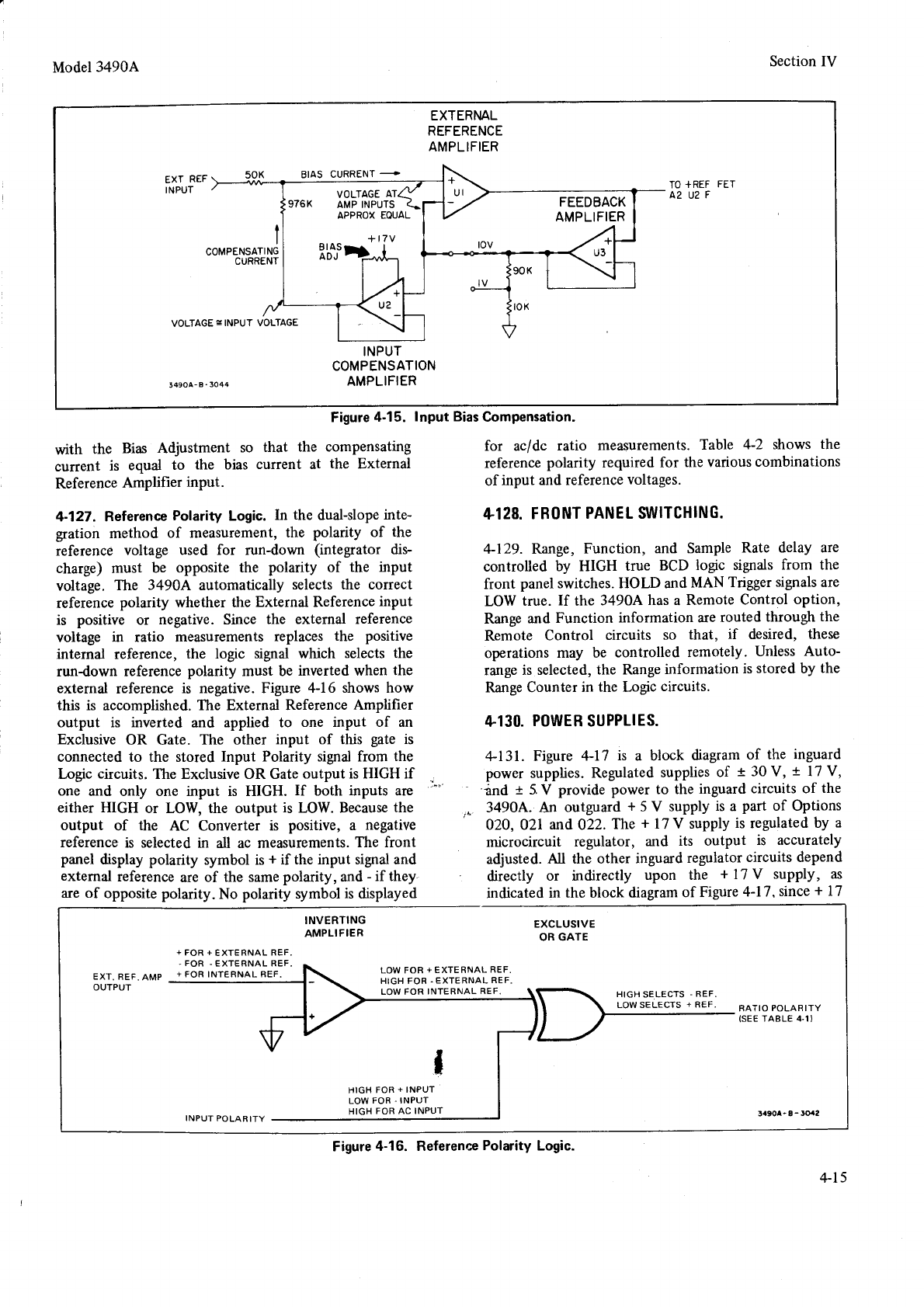
Section IV
Model3490A
EXTERML
REFERENCE
AMPLIFIER
EXT
REF
INPUT
BIAS CURRENT
+
TO
+REF
FET
A?U?F
t
I
COMPENSATING
CURRENT 90K
toK
VOLTAGE
= INPUT VOLTAGE
34904-
B
-
3044
INPUT
COMPENSATION
AMPLIFIER
VOLTAGE
AT
976K AMP INPUTS
APPROX EQUAL
+
l7v
FEEDBACK
AMPLIFIER
Figure
4-15. Input Bias
Compensation.
with the Bias Adjustment so that the compensating
current is equal to the bias current at the External
Reference
Amplifier inPut.
4-127. Reference
Polarity Logic. In the dual-slope
inte-
gration method of measurement,
the polarity of the
reference voltage used for run-down (integrator dis
charge) must be opposite the polarity of the input
voltage. The 3490A automatically selects the correct
reference
polarity whether the External Reference
input
is positive or negative. Since the external reference
voltage in ratio measurements replaces the positive
internal reference, the logic signal which selects the
rundown reference
polarity must be inverted when the
extemal reference is negative. Figure 4-16 shows how
this is accomplished.
The External Reference
Amplifier
output is inverted and applied to one input of an
Exclusive OR Gate. The other input of this gate is
connected to the stored Input Polarity signal from the
I"ogic circuits. The Exclusive OR Gate
output is HIGH if
one and only one input is HIGH. If both inputs are
either HIGH or LOW, the output is LOW. Because
the
output of the AC Converter is positive, a negative
reference
is selected
in all ac measurements.
The front
panel display polarity symbol is + if the input signal and
extemal reference
are of the same
polarity, and
- if they
are of opposite polarity. No polarity symbol is displayed
for acldc ratio measurements.
Table 4-2 shows the
reference
polarity required
for the various
combinations
of input and reference
voltages.
+128.
FBONT
PANEL S1VITCHING.
4-129. Range, Function, and Sample
Rate delay are
controlled by HIGH true BCD logic signals
from the
front panel switches. HOLD and
MAN Trigger
signals
are
LOW true. If the 3490A has
a Remote
Control option,
Range
and Function information are
routed through the
Remote Control circuits so that, if desired, these
operations
may be controlled remotely. Unless Auto-
range
is selected,
the Range
information
is stored by the
Range Counter in the Logic circuits.
4130.
POWER
SUPPLIES.
4-131. Figure 4-17 is a block diagram
of the inguard
power supplies.
Regulated
supplies
of t 30
V, t 17 V,
'änd t 5 V provide power to the inguard
circuits of the
" 3490A. An outguard
+ 5 V supply
is a part of Options
O2O, O2l andO22.
The + 17V supply
is regulated
by a
microcircuit regulator, and its output is accurately
adjusted.
All the other inguard regulator
circuits depend
directly or indirectly upon the + l7 V supply, as
indicated
in the block diagram
of Figure
4-17,
since
+ l7
INVERTING
AMPLIFIER
+
FOR
+
EXTERNAL
REF.
.
FOR
.
EXTERNAL REF.
+
FOR INTERNAL REF. LOW FOR
+
EXTERNAL
REF.
HIGH FOR
.
EXTERNAL
REF.
LOW FOR
INTERNAL
REF.
RATIO POLARITY
(SEE
TABLE 4-1)
,
I
HtGH
FOR
+
tNpUT
LOW
FOR
.
INPUT
HIGH
FOR AC INPUT
Figure
4-16. Reference
Polarity
Logic.
+t5
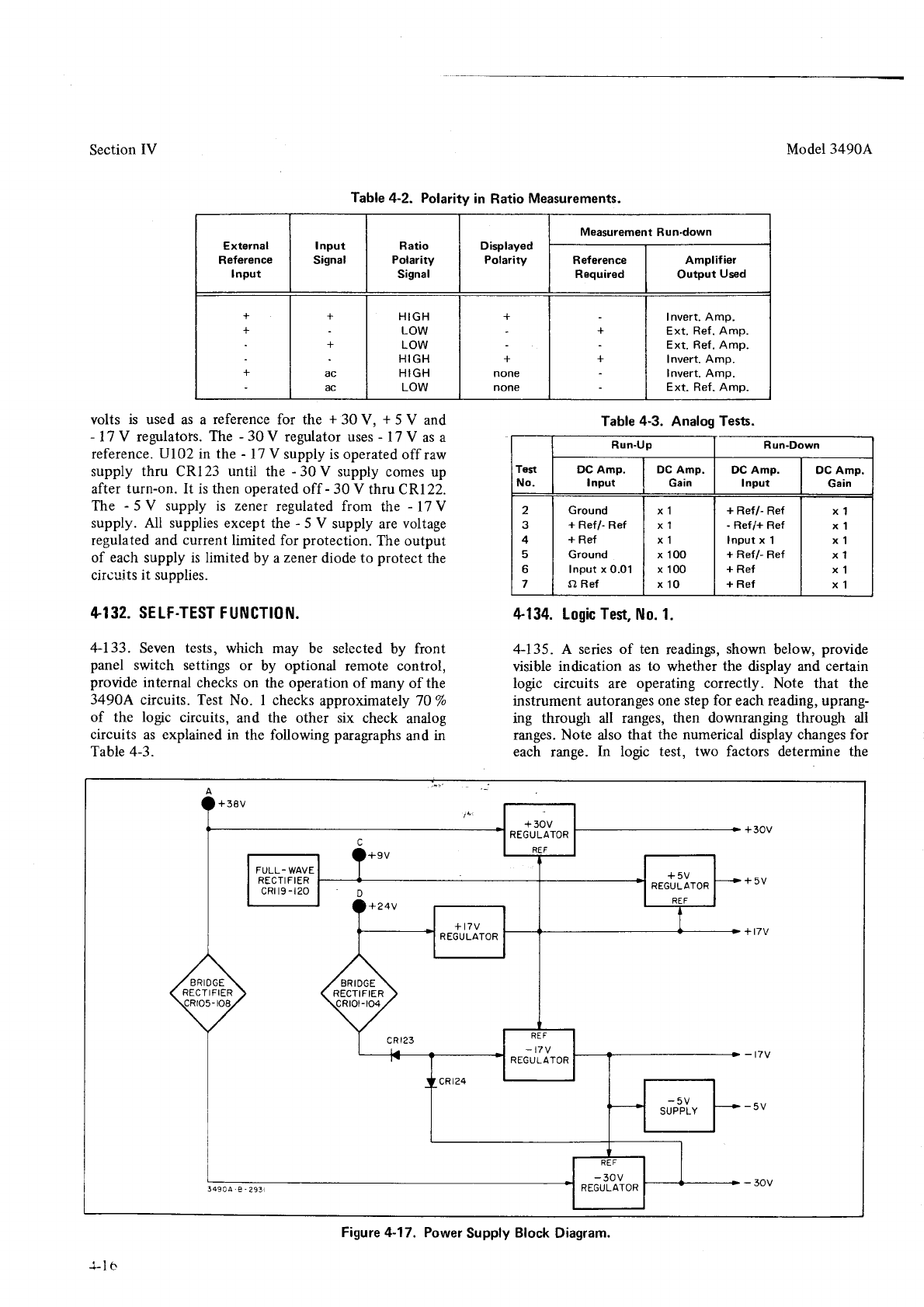
Section
IV
volts is used as a reference
for the + 30 V, + 5 V and
- 17V regulators.
The
-30V regulator uses
- 17V as a
reference. Ul02 in the
- 17 V supply is operated
off raw
supply thru CR123
until the -30V supply comes
up
after turn-on. It is then operated
off -
30 V thru CRl22.
The - 5 V supply is zener
regulated from the - l7V
supply. All supplies except
the - 5 V supply are voltage
regulated
and current
limited for protection.
The output
of each
supply is limited by a zener
diode to protect
the
circuits
it supplies.
+I32. SELF.TEST FUNCTION.
+133. Seven
tests, which may be selected
by front
panel switch settings or by optional remote control,
provide
internal
checks on the operation of many of the
3490A circuits. Test No. I checks
approximately 70%
of the logic circuits, and the other six check analog
circuits as explained
in the following paragraphs
and
in
Table 4-3.
Model
3490A
4-134.
Logic
Test,
No. l.
4-135. A series of ten readings,
shown below, provide
visible indication as to whether the display and certain
logic circuits are operating correctly. Note that the
instrument
autoranges
one
step
for each reading, uprang-
ing through all ranges,
then downranging through all
ranges. Note also that the numerical display
changes for
each range. In logic test, two factors determine
the
Table
4-2. Polarity
in Ratio
Measurements.
External
Reference
I nput
I nput
Signal
Ratio
Polarity
Signal
Displayed
Polarity
Measurement
Run-down
Reference
Required
Amplifier
Output Used
+
++
HIGH
LOW
LOW
HIGH
HIGH
LOW
+
none
none
+
Invert. Amp.
Ext. Ref. Amp.
Ext. Ref. Amp.
Invert.
Amp.
Invert. Amp.
Ext. Ref. Amp.
Table
4-3. Analog Tests.
T€sl
No.
Run-Up Run-Down
DC Amp.
Input DC Amp.
Gain DC Amp.
I nput DC Amp.
Gain
2
J
4
5
6
7
Ground
+ Ref/- Ref
+ Ref
Ground
Input
x 0.01
o Ref
x1
xl
xl
x 10O
x 100
x10
+ Ref/- Ref
- Ref/+ Ref
Input x 1
+ Ref/- Ref
+ Ref
+ Ref
x1
xl
xl
xl
x1
x1
FULL- WAVE
RECTI FIER
cRil9 - t 20
RECT IFIER
REF
REGULATOR
Figure 4-17. Power
Supply
Block
Diagram.
+lb,
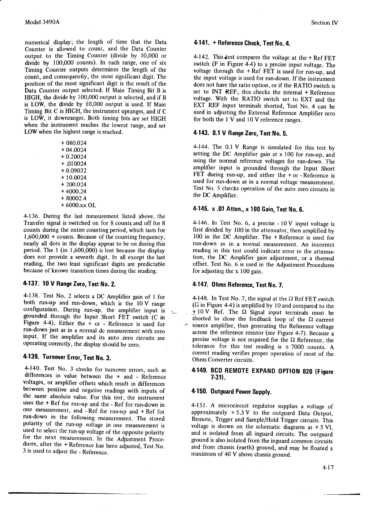
Model3490A
numerical display; the length of time that the Data
Counter is allowed to count, and the Data Counter
output to the Timing Counter (divide by 10,000 or
divide by 100,000 counts). In each range, one of six
Timing Counter outputs determines the length of the
count, and consequently,
the most significant
digit. The
position of the most significant digit is the result of the
Data Counter output selected. If Main Timing Bit B is
HIGH, the divide
by 100,000
output is
selected,
and if B
is LOW, the divide by 10,000
output is used. If Main
Timing Bit C is HIGH, the instrument upranges,
and if C
is LOW, it downranges.
Both timing bits are set HIGH
when the instrument reaches the lowest range,
and set
LOW when the highest range
is reached.
+ 080.024
+ O4.0024
+ o.2N24
+.010024
+
0.09032
+ t0.oo24
+ 200.024
+ 4000.24
+ 80002.4
+ 6000.xx
OL
4-136. During the last measurement listed above,
the
Transfer signal is switched on for 8 counts and off for 8
counts during the entire counting period, which lasts
for
1,600,000
+ counts.
Because
of the
counting
frequency,
nearly all dots in the display
appear to be on during this
period.
The I (in 1,600,000)
is lost because the display
does not provide a seventh
digit. In all except the last
reading, the two least significant digits are predictable
because
of known transition times during the reading.
+137.
10
V Range
Zero,Test
No.
2.
4.138. Test No. 2 selects
a DC Amplifier gain
of I for
both run-up and run-down, which is the l0 V range
configuration. During run-up, the amplifier input 1s
grounded through the Input Short FET switch (C in
Figure 44). Either the + or - Reference is used for
run-down just as in a normal dc measurement
with zero
input. If the amplifier and its auto zero circuits are
operating
correctly, the display
should
be zero.
4139. Turnover
Error,
Test
No.
3.
4-140. Test No. 3 checks
for turnover errors, such
as
differences in value between the + and - Reference
voltages,
or amplifier offsets which result in differences
between positive and negative
readings
with inputs of
the same absolute value. For this tesi, the instrument
uses
the + Ref for run-up and the - Ref for run_down
in
one measurement,
and _
Ref for run_up and + Ref for
run-down in the following measuremänt. The stored
pola.rity of the run-up voltage in one measurement
is
used
to select
the
run-up
voltage
of the opposite polarity
for the next measurement.
ti tne RAiustmenf
proce_
dures,
after the + Reference
has
been
adjusted, Test
No.
3 is
used
to adjust
the
- Reference.
Section
IV
4141.
+
Reference
Check, Test
No.
4.
4-142.
Tlnslest
compares
the
voltage
at the
+
Ref
FET
switch (F in Figure 44) Io a precise
input voltage. The
voltage through the + Ref FET is used
for run-up, and
the input voltage is used
for run-down. If the instrument
does
not have the ratio option, or if the RATIO switch is
set to INT REF, this checks the internal + Reference
voltage. With the RATIO switch set to EXT and the
EXT REF input terminals shorted, Test No. 4 can be
used
in adjusting the External Reference
Amplifier zero
for both the I V and
l0 V reference
ranges.
+143.
0.1V Range
Zero,
Test
No.
b.
4-144. The 0.1
V Range is simulated
for this test by
setting the DC Amplifier gain at x 100 for run-up, and
using the normal reference
voltages
for run-down. The
amplifier input is grounded through the Input Short
FET during run-up, and either the + or - Reference
is
used
for run-down
as
in a normal
voltage
measurement.
Test
No. 5 checks
operation
of the auto zero
circuits
in
the DC Amplifier.
4145.
x .01 Atten.,
x
100
Gain,
Test
No.
6.
4146. In Test No. 6, a precise
- l0 V input voltage
is
first divided
by 100
in the
attenuator,
then
amplified
by
100 in the DC Amplifier. The + Reference
is used
for
run-down as in a normal measurement.
An incorrect
reading in this test could indicate
error in the attenua-
tion, the DC Amplifier gain adjustment,
or a thermal
offset.
Test
No. 6 is used
in the Adjustment
procedures
for adjusting
the
x 100
gain.
4147.
0hms Reference,
Test
No.
7.
,l-148. In Test
No. 7, the
signal
at the Q Ref FET switch
(G
in Figure
44) is amplified
by l0 and compared
to the
.tlOv Ref. The A Signal input terminals must be
shorted to close the feedback
loop of the e cunent
source
amplifier, thus generating
the Reference
voltage
across the reference
resistor
(see
Figure
4-7). Because
a
precise
voltage
is not required for the fl Reference,
the
tolerance for this test reading
is I 7000 counts. A
correct
reading
verifies proper
operation
of most of the
Ohms
Converter
circuits.
+149. BCD
REMOTE
EXPAND
0PTt0N
020
(Figure
7-3r).
4150.
0utguard
Power
Supply.
4-151. A microcircuit regulator
supplies
a voltage of
approximately + 5.3
V to the outguard Data Output,
Remote, Trigger and Sample/Hold
Trigger circuits. This
voltage is shown on the schematic diagrams
as + 5 VI,
and is isolated from all inguard circuits. The outguard
ground
is
also isolated
from the
inguard
common
circuits
and from chassis
(earth) ground,
and
may be floated a
maximum of 40 V above
chassis
sround.
+17
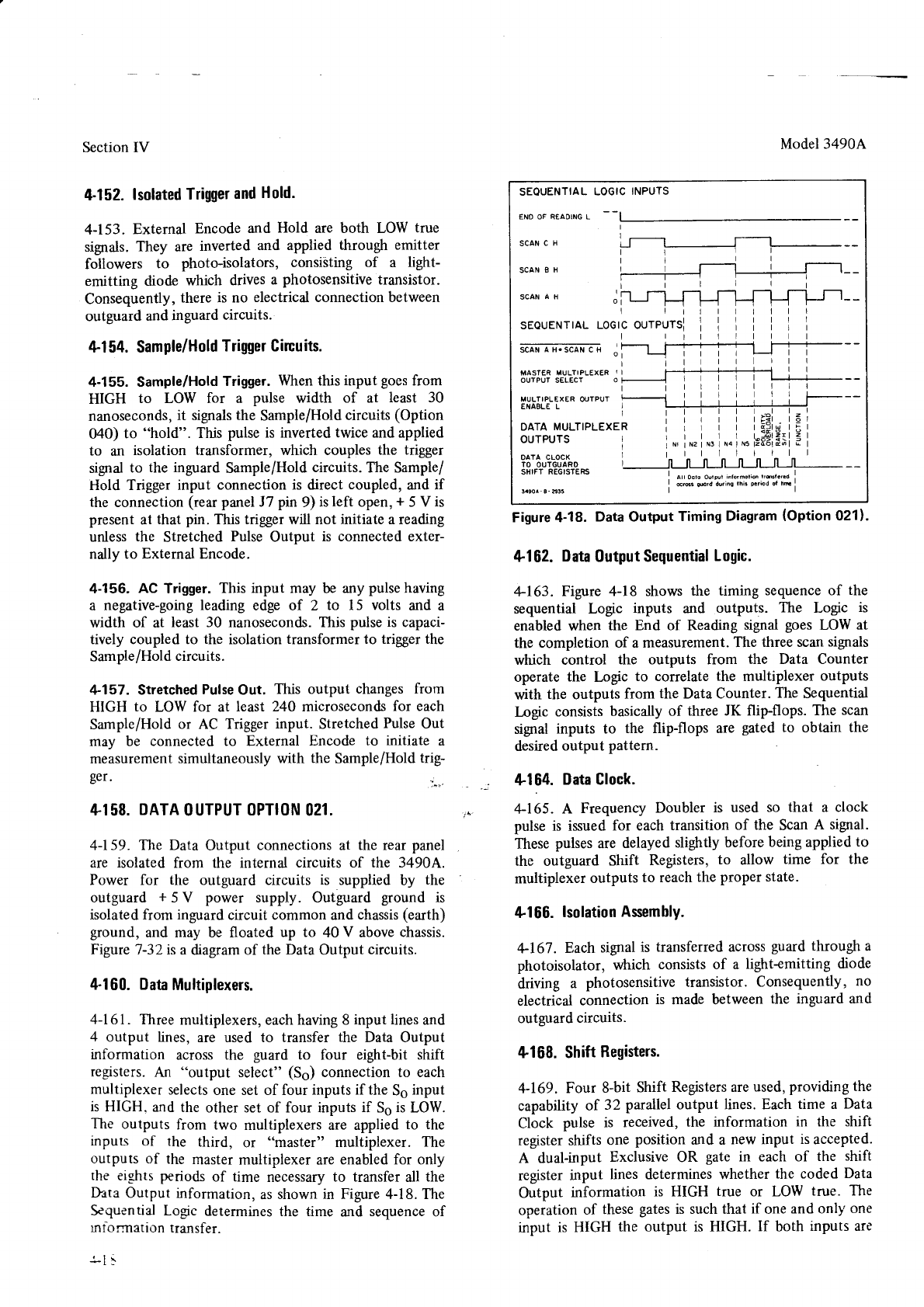
Section IV
4-152.
lsolated
Trigger
and
Hold.
4-153. External Encode
and Hold are both LOW true
signals.
They are inverted and applied through emitter
followers to photo-isolators, consisting of a light-
emitting diode which drives
a photosensitive
transistor.
Consequently,
there is no electrical connection between
outguard and
inguard
circuits.
It-l54.
Sample/Hold
Trigger Circuits.
4-155. Sample/Hold
Trigger.
When this
input goes
from
HIGH to LOW for a pulse width of at least 30
nanoseconds,
it signals
the Sample/Hold
circuits
(Option
040) to "hold". This pulse is inverted twice and applied
to an isolation transformer, which couples the trigger
sigral to the inguard Sample/Hold
circuits. The Sample/
Hold Trigger input connection is direct
coupled,
and if
the connection
(rear
panel
J7 pin 9) is
left open,
+ 5 V is
present at that pin. This trigger
will not initiate a reading
unless
the Stretched
Pulse
Output is connected exter-
nally to External Encode.
4-156. AC Trigger. This input may be any pulse
having
a negative-going leading
edge of 2 to 15 volts and a
width of at least 30 nanoseconds.
This
pulse is capaci-
tively coupled to the isolation transformer to trigger the
Sample/Hold
circuits.
zt-157.
Stretched
Pulse
Out. This output changes from
HIGH to LOW for at least 240 microseconds
for each
Sample/Hold
or AC Trigger
input. Stretched
Pulse
Out
may be connected to External Encode to initiate a
measurement
simultaneously with the Sample/Hold
trig-
ger.
+158.
DATA
OUTPUT
OPTION
021.
4-159. The Data Output connections at the rear
panel
are isolated from the internal circuits of the 3490^.
Power for the outguard circuits is supplied by the
outguard + 5 V power supply. Outguard ground is
isolated from inguard
circuit common and
chassis
(earth)
ground, and may be floated up to 40 V above
chassis.
Figure 7-32 is a diagram of the Data Output circuits.
4-160. Data
Multiplexers.
4-161 . Three
multiplexers, each having 8 input lines
and
4 output lines,
are used to transfer the Data Output
information across the guard to four eight-bit shift
registers.
An "output select" (Ss) connection to each
multiplexer
selects
one set of four inputs if the Ss
input
is HIGH. and the other set of four inputs
if Se
is LOW.
The outputs from two multiplexers are applied
to the
inputs of the third, or "master" multiplexer. The
outputs of the master
multiplexer are
enabled for only
the eights periods
of time necessary
to transfer
all the
Data
Output information,
as
shown
in Figure 4-1 8. The
Sequential Logic determines
the time and sequence
of
mlolTnation
transfer.
:-l !
SEOUENTIAL
LOGIC
INPUTS
ENO OF REAOING L
SCAN
C H
SCAN
8 H
I
MASTER MULTIPLEXER I I
OUTPUT SELECT O
I
IIULTIPL€XER OUTPUT I
ENAELE L I
I
SCAN A H
DATA
MULTIPLEXE
OUTPUTS
OATA CLOCK
IO OUTGUARO
SHIFT
REGISTERS
ltllllt
rnnnnnnnn
I o,,oo,o outou, i.lormorion tcl.r.d I
I oc.cr ry'd ddihq rhi. e.riod d iß i
lltlttlltr
courPursl
I i I i i I I
lL--1t..
I lEXr-19
| | dild I F
i i 16i9'i
3
i"r i98äiä;i
i
lll
lll
rrirztn:lla
Figure 4-18. Data Output Timing
Diagram
(Option
021
).
4-162.
Data
Output Sequential
Logic.
zt-163.
Figure 4-18 shows
the timing sequence of the
sequential Logic inputs and outputs. The Logic is
enabled when the End of Reading
signal goes LOW at
the completion of a measurement.
The three scan
signals
which control the outputs from the Data Counter
operate the Logic to correlate the multiplexer outputs
with the outputs from the Data Counter. The Sequential
Logic consists
basically
of three JK flipflops. The scan
signal inputs to the flip-flops are gated to obtain the
desired
output pattem.
4164. Oata Clock.
+165. A Frequency
Doubler is used so that a clock
pulse is issued for each
transition of the Scan
A signal.
These
pulses
are delayed
slightly before
being applied
to
the outguard Shift Registers,
to allow time for the
multiplexer
outputs
to reach
the
proper state.
4166.
lsolation
Asembly.
arl67. Each
signal
is transferred across
guard through
a
photoisolator, which consists of a light+mitting diode
driving a photosensitive
transistor.
Consequently,
no
electrical connection is made between the inguard and
outguard
circuits.
+168. Shift
Registers.
4-169. Four 8-bit Shift Registers are
used,
providing the
capability
of 32 parallel output lines. Each
time a Data
Clock pulse is received, the information in the shift
register shifts
one position
and a new input is
accepted.
A dual-input Exclusive
OR gate in each of the shift
register
input lines determines whether
the coded
Data
Output information is HIGH true or LOW true. The
operation
of these
gates
is such that if one
and only one
input is HIGH the output is HIGH. If both inputs are
Model 34904
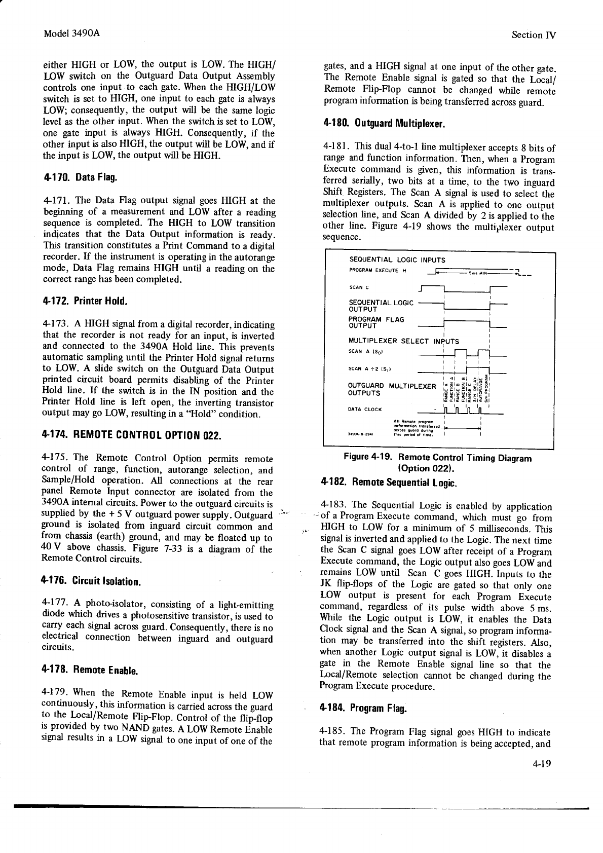
Model
34904
either HIGH or LOW, the output is LOW. The HIGH/
LOW switch on the Outguard Data Output Assembly
controls one input to each
gate.
When
the HIGH/LOW
switch is set to HIGH, one input to each
gate
is always
LOW; consequently, the output will be the same logic
level as
the other input. When
the switch is set
to LOW,
one gate input is always HIGH. Consequently, if the
other input is also
HIGH, the output will be LOW, and if
the input is LOW, the output will be HIGH.
4170. Data
Flag.
+171. The Data Flag output signal
goes
HIGH at the
begiruring of a measurement
and LOW after a reading
sequence
is completed. The HIGH to LOW transition
indicates that the Data Output information is ready.
This transition constitutes a Print Command to a digital
recorder. If the instrument is operating
in the autorange
mode, Data Flag remains HIGH until a reading
on the
correct range has been completed.
L172. kinter Hold.
+173. A HIGH signal
from a digital
recorder,
indicating
that the recorder is not ready for an input, is inverted
and connected to the 349OA Hold line. This prevents
automatic sampling
until the Printer Hold signal
returns
to LOW. A slide switch on the Outguard Data Output
printed circuit board permits disabling of the printer
Hold line. If the switch is in the IN position and the
Printer Hold line is left open, the inverting transistor
output may go LOW, resulting
in a ..Hold" condition.
4t74.
REM0TE
C0NTR0t
0PTtoN
022.
+175. The Remote Control Option permits remote
control of range, function, autorange
selection,
and
Sample/Hold operation. All connections at the rear
panel Remote Input connector are isolated from the
34g0{internal circuits. Power
to the outguard
circuits is
supplied
by the + 5 V outguard
power supply. Outguard ,r-.
ground is isolated from inguard circuit common and
from chassis
(earth) ground, and may be floated up to
40 V above chassis.
Figure 7-33 is a diagram of the
Remote
Control circuits.
l}176.
Gircuit
lsolation.
1.177. A photo-isolator,
consisting
of a light-emitting
diode which drives
a photosensitivJtransistoi,
is used to
carry
each
signal
across
guard.
Consequently,
there
is
no
electrical connection bätween inguärd and outguard
circuits.
4-178.
Remore
Enable.
4-179. When the Remote Enable
input is held LOW
continuously, this information is carrieä
across the guard
to the bcal/Remote FlipFlop. Control of the flif_flop
is provided
by two NAND gates.
A LOW
Remote Enable
signal
results
in a LOW siglral
to one
input of one of the
Section
IV
gates,
and a HIGH signal
at one input of the other gate.
The Remote Enable signal is gated so that the fwa[
Remote Flip-Flop cannot be changed while remote
program
information is being transferred
across guard.
4180.
0utguard
Multiplexer.
4181. This
dual
4-to-1
line
multiplexer
accepts
g bits of
range and function information. Then, when a progam
Execute command is given, this information is trans-
ferred serially, two bits at a time, to the two inguard
Shift Registers.
The Scan A signal
is used
to selecl the
multiplexer outputs. ftan A is applied to one output
selection
line, and Scan
A divided
by 2 is
applied
toihe
other line. Figure 4-19 shows the multiplexer output
sequence.
SEOUENTIAL
LOGIC INPUTS
PROGRAM
EXECUTE
H
scat{ c
SEOUENTIAL
LOGIC
-----_-I
OUTPUT
PROGRAM
FLAG
OUTPUT I
I
ll
MULTIPLEXER
SELECT
INPUTS I
ll
scaNA(So) | r---l
-tlttl
SCAil A +2 (S,}
r <t ., :,'Ei
oUTGUARD
MULnpLEXER
i"
6:"
6i";lä
g
ourPurs g!9!;?;Fi
rä,?rE
i,ä ,)ri
Sr
oara
cLocK ___:-_tt_tl_lt_lt__
ll
A[ R.hot. doCroh | |
'nrdmoron ronrt.'r.d i -
crd. ouo.a öuri^o
!.sr.s te.r tht. r.nod ot r,m.- | |
Figure
4-19. Remote
Control
Timing
Diagram
(Option
022).
4182. Remote
Sequential
Logic.
zl-183.
The Sequential
Itgic is enabled
by application
'-'of a Program
Execute
command, which musf go from
signal
is inverted
and applied
to the Logic. The
next time
the Scan
C signal goes
LOW after receipt of a progam
Execute
command,
the Ingic output also
goes
LOW
and
remains
LOW until Scan C goes
HIGH. Inputs to the
JK flip-flops of the Logic are gated so that only one
LOW output is present for each program Execute
command, regardless
of its pulse width above 5 ms.
While the Logic output is LOW, it enables
the Data
Clock signal
and the Scan A signal,
so program
informa-
tion may be transferred
into the shift registers.
Also,
when another logic output signal
is LOW, it disables
a
gate in the Remote Enable signal line so that the
Iocal/Remote selection
cannot be changed
during the
Program
Execute
procedure.
+184.
Program
Flag.
4-185. The Program
Flag signal
goes
HIGH to indicate
that remote program
information
is being
accepted,
and
+r9
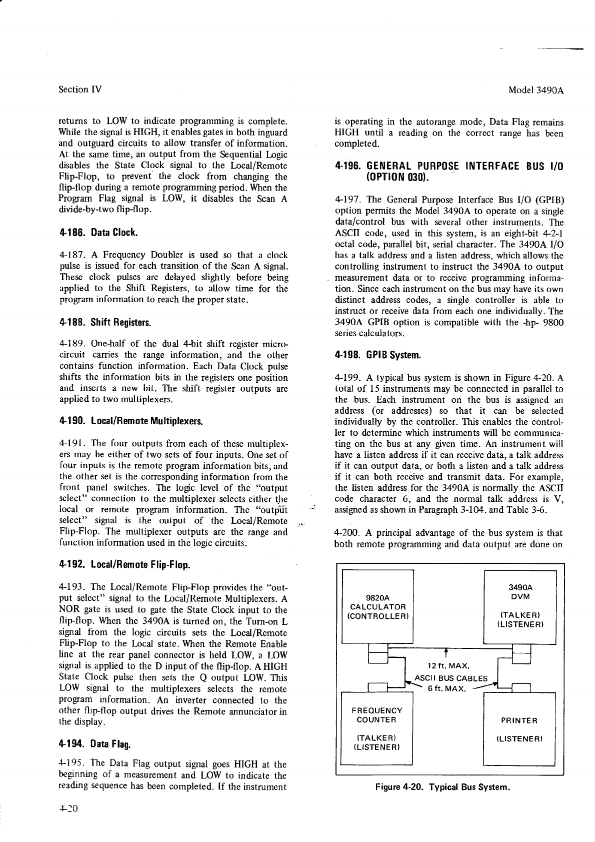
Section IV
returns to LOW to indicate
programming
is complete.
While the signal is HIGH, it enables
gates
in both inguard
and outguard circuits to allow transfer of information.
At the same time, an output from the Sequential
l,ogic
disables the State Clock signal to the t-ocal/Remote
Flip-Flop, to prevent the clock from changing the
flip-flop during a remote programming
period, When the
Program Flag signal is LOW, it disables
the Scan A
divide-by-two flip-fl op.
4186. Data Clock.
+187. A Frequency Doubler is used so that a clock
pulse is issued for each transition of the Scan
A signal.
These clock pulses are delayed slightly before being
applied to the Shift Registers, to allow time for the
program
information to reach
the proper
state.
+188. Shift
Registers.
+189. One-half of the dual 4-bit shift register
micro-
circuit carries
the range information, and the other
contains function information. Each Data Clock pulse
shifts the information bits in the registers one position
and inserts a new bit. The shift register outputs are
applied to two multiplexers.
41 90. Local/Remote
Multiplexers.
+191 . The four outputs
from each of these
multiplex-
ers may be either
of two sets of four inputs.
One
set
of
four inputs is the remote program
information
bits, and
the other set
is the corresponding
information from the
front panel switches.
The logic level of the "output
select" connection
to the multiplexer selects
either
{he
local or remote program information. The "outpüi
select" signal is the output of the Local/Remote
Flip-Flop. The multiplexer outputs are the range
and
function information
used in the logic
circuits.
4-1
92. LocaURemote
Flip-Flop.
4-193. The Local/Remote
Flip-Flop provides
the "out-
put select" signal
to the Incal/Remote Multiplexers.
A
NOR gate
is used to gate the State Clock input to the
flip-flop. When the 3490A is turned on, the Turn-on L
signal from the logic circuits sets the Local/Remote
Flip-Flop to the local state.
When the Remote Enable
line at the rear panel
connector
is held LOW, a L,OW
sigtal is applied
to the D input of the
flip-flop. A HIGH
State Clock pulse
then sets
the Q output LOW. This
LOW signal to the multiplexers selects the remote
program information. An inverter connected
to the
other flip-flop output drives
the Remote annunciator in
the display.
4194. Dau
Flag.
t195. The Data Flag output signal goes
HIGH at the
begrnning
of a measurement
and LOW to indicate
the
reading sequence
has
been
completed.
If the
instrument
+10
Model3490A
is operating
in the autorange
mode, Data Flag
remains
HIGH until a reading on the correct range
has been
completed.
4.196.
GENERAL
PURPOSE
INTERFACE
BUS
I/O
(0PTtoN
030).
4-197. The General Purpose
Interface Bus I/O (GPIB)
option permits the Model 3490A to operate on a single
data/control bus with several other instruments.
The
ASCII code, used in this system, is an eight-bif +2-l
octal code,
parallel
bit, serial character. The 3490A I/O
has
a talk address
and a listen
address, which allows
the
controlling instrument
to instruct the 3490A to output
measurement
data or to receive
programming
informa-
tion. Since each
instrument on the bus may have
its own
distinct address codes,
a single controller is able to
instruct or receive
data from each one individually. The
3490A GPIB option is compatible with the -hp- 9800
series calculators.
4-198.
GPIB
System.
4-199. A typical bus
system is shown in Figure
4-20. A
total of 15 instruments
may be connected
in parallel
to
the bus. Each instrument on the bus is assigred an
address (or addresses) so that it can be selected
individually by the controller. This enables the control-
ler to determine which instruments will be communica-
ting on the bus at ury given time. An instrument will
have
a listen
address
if it can
receive
data, a
talk address
if it can output data, or both a listen
and
a
talk address
if it can both receive and transmit data. For example,
the listen address for the 3490A is normally the ASCII
code character
6, and the normal talk address
is V,
assigned as shown
in Paragraph
3-104.
and
Table
3-6.
4-200. A principal
advantage of the bus system is that
both remote
programming
and data output are done on
9820A
CALCULATOR
(CONTROLLER}
3490A
DVM
(TALKE
R}
(LISTENERI
FREOUENCY
COUNTER
(TALKER}
(LISTENERI
PR
INTE
R
(LISTENER}
12
ft. MAX.
ASCII
8US
CABLES
Figure
4-20. Typical Bus System.
Model3490A
the same data lines. For this reason a standard
cable
(which may be various
lengths)
is used to connect
each
instrument to the bus. The cable contains
eight data
lines and
seven
control
lines.
4201. Basic
Theory
of GPIB
l/0 Circuits.
4-202. The
3490A GPIB
circuits employ
two separate
logic systems
called Algorithmic Siate Machines (ASM).
A brief explanation of an Algorithmic State
Machine is
given in Parugraph
4-90. One ASM is inside the instru-
ment guard (Inguard State Machine) and the other is
outside the guard (Outguard State Machine). Each
system must accept, store, and output information,
providing a two-way communication link between the
3490A internal logic circuits and the other bus system
instruments. The two State Machines are timed by
separate free-running clocks;
consequently,
communica-
tion between
the two machines
is asynchronous.
Figure
736 is a block diagram of the GPIB
I/O circuits.
Table
3-5 lists
the bus signal mnemonics.
4-203. Information is transferred across
guard
from one
ASM to the other by means
of photo-transistors,
so that
there is no electrical contact between inzuard and
outguard circuits.
This
allows the inguard
anä'outguard
circuits to operate on different ground systems at
different potentials. The outguard ASM receives
and
interprets information from the controller. It then
responds
to the controller, and transfers the necessary
information across
guard to the inguard ASM, which
programs
the 3490A logic circuits. When
the instrument
is addressed
to talk, the measurement
output data is
transferred across guard one digit or character
at a time.
P11u
Ir then placed
on the bus
data lines
DIOI through
DI07 one character at a time in the sequence
shown in
Paragaph 3-126. Tlre timing of the data output is
controlled by the three "handshake" sigrals
described
in
Paragraphs
3-94 through 3-97.
4-204.
GPIB
System
Operation.
4-2-O!. Reset. When power is first applied to the
3490A, the Reset circuit output is LOW for approxi-
mately 100
ms. This sets
the inguard ASM to the-,izero,'
state,.and sets the range
and function circuits to the
front panel settings.
It also
clears
the Sample/Hold and
Remote storage
flip-flops and the trigger mode, causing
all programming to conform to the fiönt panel
settingsl
The outguard ASM circuits then check io see if the
3490A logic circuits indicate that the instrument is in
remote control. If not, the instrument
continues
to be
controlled
from the
front panel.
+246. Local Control. In local control, the I/O circuits
accept and store range and function information from
the front panel.
Sample
Rate
and Sample/Hold
(option_
al) are controlled
from the
front panel.-This
information
may be updated at any time by changing
the control
s€ttings.
If the Sample
Rate
control ls set to HOLD, the
Section
IV
3490A may be triggered
through the rear panel Trigger
connector.
If addressed
to talk, the 3490A will output
measurement data in accordance with normal bus
operation.
4-2O7. Address to Listen. When the Outguard State
Machine senses
that the MRE line is LOW, it waits for
DAV to go LOW indicating that the data
information is
valid. When
LDAV is received,
data lines
DI05 through
DIOI are compared
to the 34904 address
bits. If thöv
match,
DI07 is checked
to determine
if the address
is
tä
talk or to listen. If DI07 is HIGH, the 3490A is
addressed
to listen. It then checks
REN to see
if it is
LOW. If so, the internal RMT line is set LOW and this
information is transferred
across guard and the Inguard
State Machine sets the 3490A to remote control,
disabling
the front panel
range,
function, and Samplef
Hold controls.
As soon
as
the address
data
and
tn, fiBN
line have
been
checked,
the DAC output is allowed
to go
HIGH,
indicating
that the data has
been
accepted.
4-208. Remote Programming.
After the 3490A has
been
instructed
to listen and placed
in remote
control.
the controller sets
MRE High so that the 3490A can
receive
remote
program
data. This data is placed
on the
seven
data lines
DI0l -7 by the
controller,
one
character
at a time. After each character
is placed
on the data
lines,
the controller
sets
DAV to LOW, indicating
to the
349OA
Outguard
State Machine
that this data iJ readv.
The Outguard
State
Machine
checks
to see if the datals
valid for the 3490A and then transfers
the data across
guard
to the Inguard
State Machine.
It also sets
the DAC
line HIGH and RFD LOW to indicate
that the data
has
99rl accepted
and
is being processed.
The
Inguard
State
Machine
then interprets
the data
and takes
appropriate
action. For example,
if the character
received
is the
alpha
identifier R, the
inguard
circuits
are set
so that the
next character
(if it is a digit) is routed to the ranse
storage
circuit. (See Paragraph
3-106 for the ..rnol.
programming
sequence.)
After a data
character
has
been
' 'i processed,
RFD is
allowed to go
HIGH, ind"icating
to the
iL controller
that the 3490A
is
ready for new data.
4-209. When
programming
is completed,
the controller
must send
the ASCII code character
E, after which it
may address
the 34904 to talk or it may address
anv
other
unit on the
bus to listen
or talk.
The
character
6
indicates
to the 3490A that the progamming is ended.
The 3490A then will not accept any more data until
after
MRE has
again
been
set
LOW
and
the 3490A listen
address
sent.
4-210. Address
to Talk. When the 3490A
is addressed
to talk, it outputs the measurement
data in the format
shown in Paragraph 3-126. The output sequence is
controlled by the Inguard State Machine tlirough a
multiplexer and a storage
unit. As each output data
character is transferred across guard, the öutguard
circuits place this character on the data lines and set
DAV to LOW,
indicating to the listener
that valid data is
available.
When the listener sets
DAC HIGH, indicating
+2r
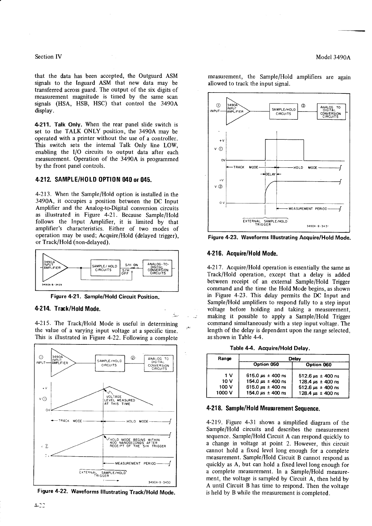
Section
IV
that the data has been accepted, the Outguard ASM
signals to the Inguard ASM that new data may be
transferred across
guard. The output of the six digits of
measurement magnitude is timed by the same scan
signals (HSA, HSB, HSC) that control the 3490A
display.
4-211. Talk Only. When
the rear panel
slide switch is
set to the TALK ONU/ position, the 34904 may be
operated with a printer without the use
of a controller.
This switch sets the internal Talk Only line LOW,
enabling the I/O circuits to output data after each
measurement. Operation
of the 3490A is programmed
by the front panel
controls.
+212.
SAMPLE/H0tD 0PTl0N ll40
or
045.
4-213. When the SampleiHold
option is installed in the
3490^, it occupies
a position between
the DC Input
Amplifier and the Analog-to-Digital conversion
circuits
as illustrated in Figure 4-21 . Because Sample/Hold
follows the Input Amplifier, it is limited by that
amplifier's characteristics.
Either of two modes of
operation may be used; Acquire/Hold
(delayed
trigger),
or Track/Hold
(non-delayed).
Figure 4-21.
Sample/Hold
Circuit Position.
4-214. Twk/Hold Mode. __-"
4-215. The Track/Hold Mode is useful in determining
the value of a varying input voltage
at a specific
time.
This is illustrated
in Figure 4-22.Following a complete
FiEure 4-22. Waveforms
lllustrating
Track/Hold
Mode.
1-ll
Model3490A
measurement, the Sample/Hold amplifiers are again
allowed to track the
input signal.
HoLo MooE
--._J
MEASUREMEN,
pERroD
_Jf
EXTERNAL
SAMPLE/HOLD
TRIGG
ER 34904 B'3411
Figwe
4-23. Waveforms
lllustrating
Acquire/Hold
Mode.
4-216.
Acquire/Hold
Mode.
4-217. Acquire/Hold
operation is essentially
the same
as
Track/Hold operation, except that a delay is added
between receipt of an external Sample/Hold Trigger
command
and the time the Hold Mode
begins, as shown
in Figure 4-23. This delay permits the DC Input and
Sample/Hold amplifiers
to respond
fully to a step input
voltage before holding and taking a measurement,
making it possible to apply a Sample/Hold Trigger
command simultaneously
with a step input voltage.
The
lengih
of the delay
is
dependent upon the
range selected,
as shown
inTable 44.
Table
44. Acquire/Hold Delay.
Range Delav
Option 050 Option 060
1V
10v
100 v
1000 v
615.0rts1400ns
154.0
ps t 400
ns
615.0
rrs
t 400 ns
154.0
ps t 400
ns
512.6
ps
t 400
ns
128.4 tts
t 4p0 ns
512.6
trs
i zl00
ns
128,4 tts
+ 400 ns
4-21
8. Sample/Hold
Mea$rement
Sequence.
4-219. Figure 4-31 shows a simplified diagram of the
Sample/Hold
circuits and describes
the measurement
sequence.
Sample/Hold Circuit A can
respond
quickly to
a change in voltage at point 2. However, this circuit
cannot hold a fixed level
long enough
for a complete
measurement.
Sample/Hold
Circuit B cannot
respond as
quickly as
A, but can
hold a fixed level
long
enough for
a complete measurement.
In a Sample/Hold measure-
ment, the voltage
is sampled
by Circuit A, then
held by
A until Circuit B has time to respond. Then the voltage
is
held by B while
the
measurement
is completed.
ANALOG
TO
DIGITAL
CONVER
SION
CIRCUITS
VOLTAGE
LEVEL MEASURED
AT THIS
TIME
+TRACK MOoE
O MODE EEGINS WITHIN
NANOSECONOS
AFTER
ElPT OF THE S/H TRIGGER
MEA5gREMENT
pERroD- -/
iX]ER^iAL SAMPLE/HOLD
TRIGGER
1490a'B 3430
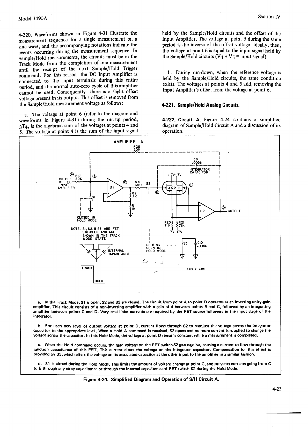
Model3490A
4:220. Waveforms shown in Figure 4-31 illustrate the
measurement
sequence
for a single measurement
on a
sine wave,
and the accompanying
notations indicate
the
events occurring during the measurement
sequence'
In
Sample/Hold measurements,
the circuits must be in the
Traci Mode from the completion of one measurement
until the receipt of the next Sample/Hold Trigger
command. For this reason' the DC Input Amplifier is
connected to the input terminals during this entire
period, and the normal auto-zero
cycle of this amplifier
iatrnot be used. Consequently, there is a slight offset
voltage
present
in its output. This offset is-removed
from
the Sample/Hold
measurement
voltage
as follows:
a. The voltage at point 6 (refer to the diagram
and
waveforms in Figure 4-31) during the run-up period,
3T4, is the algebraic
sum of the voltages at points 4 and
S. nre voltage at point 4 is the sum of the input signal
Section
IV
held by the Sample/Hold circuits and the offset of the
Input Amplifier. The voltage at point 5 during the same
period is the inverse of the offset voltage. Ideally, then,
the voltage at point 6 is equal
to the input signal
held by
the Sample/Hold
circuits (V4 + V5 = input signal).
b. During run-down, when the reference
voltage is
held by the Sample/Hold circuits, the same condition
exists.
The voltages
at points 4 and 5 add, removing
the
Input Amplifier's offset from the voltage at point 6.
&221. Sample/Hold
Analog
Circuits.
4-222. Circuit A. Figure 424 contuns a simplified
diagram of Sample/Hold Circuit A and a discussion
of its
operation.
AMPLIFIE R A
O 83" sz
INTEGRATOR
+t7vrt7V cAPAclroR
@
n'z
OUTPUT
zOK
OF DC+
INPUT
AMPLIFIER
R20
7t
KR2l
7tK
NOTEr Sl,S2,A53
ARE
FET
SWITCIES,
AND ARE
STIOWN
IN THE TRACK
MODE STATE
T.
l-
'.,r,*f v-tNTERNAL
-... | _,^ CAPACTTANCE
\,,
-t7v
3490-8 - l39l
a. In the
Track Mode,
Sl is
open,
52
and 53
are
closed.
The
circuit from point
A to point D operates as
an
inverting
unity€ain
amplifier. This circuit consists
of a non-inverting amplifier with a gain of 4 between
points B and C, followed by an
integrating
amplifier between points C and D. Very small
blas
currents
are required
by the FET source-followers
in the input stage
of the
integrator.
b. For each nar level of output voltage
at point D, current flows through 52 to readjust the \roltage across
the integrator
capacitor
to the appropriae level.
When
a Hold A command is received,
52 opens and no more current is supplied
to chang€
the
\toltage
across
the capacitor,
ln this Hold Mode,
the voltage
at point D remains constant while a measurement is
complEted.
c. When
the Hold comnrand
occurs, the gate
voltage on the FET switch
52 goes
rcgatiw,
causing
a current to flow through the
iunction capacitance
of this FET. This current alters the \roltage
on the integrator capacitor. Compensation
for this effect is
provided
by 53, which alters
the voltage on its associated
capacitor at the other input to the amplifier in a similar
fashion.
d. Sl is
closed
during
the Hold Mode.
This
limits the amount of voltage
change
at point
C, and
prevents
currents
going
from C
to E through
any
stray capacitance
or through
the internal
capacitance
of FET switch
52
during the Hold Mode.
-LCIO
T'oo
I
v
56
Figure
4-24. Simplified
Diagram and Operation of S/H Circuit A.
+23
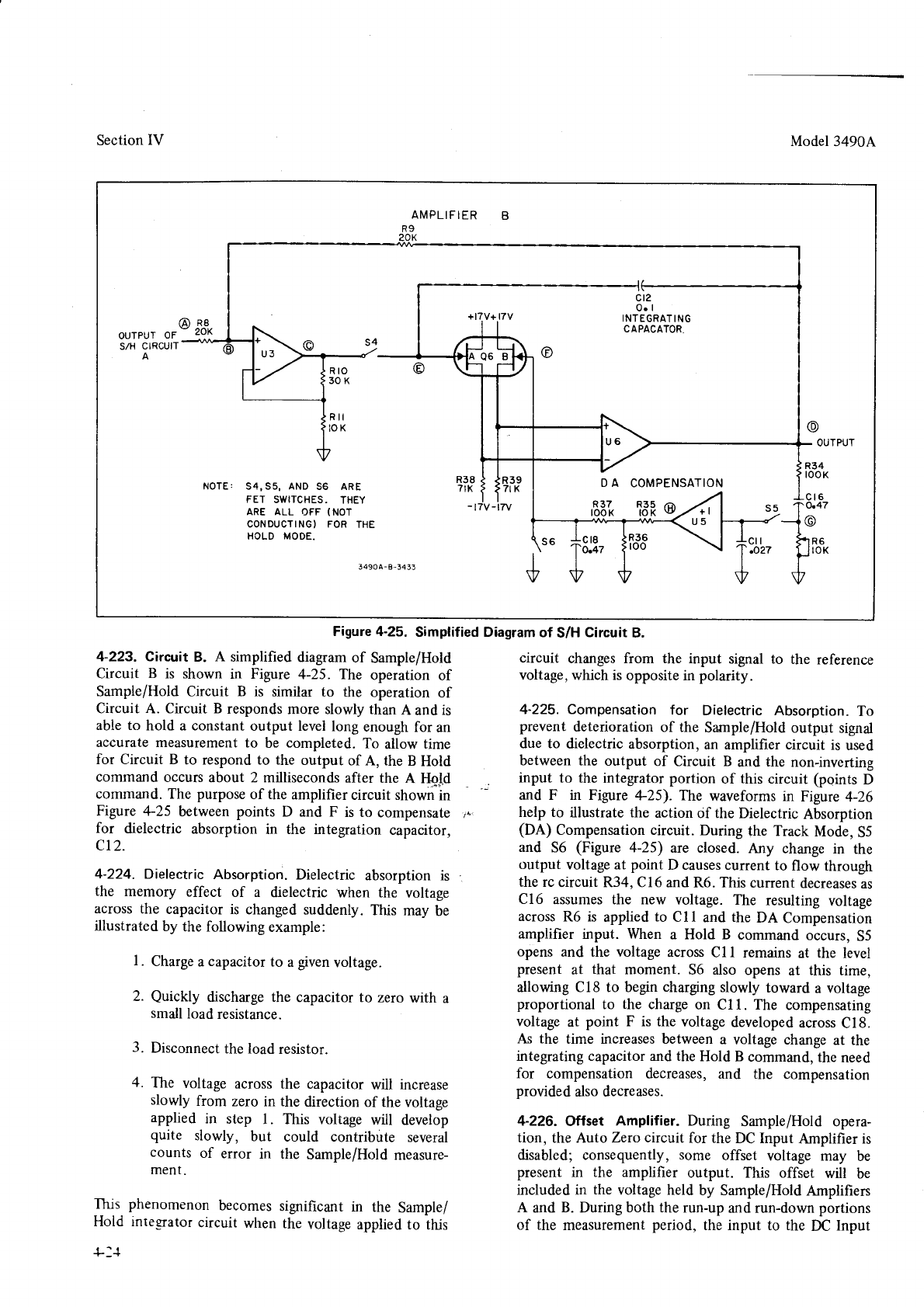
Section
IV
4-223. Circuit B. A simplified
diagram
of Sample/Hold
Circuit B is shown in Figure 4-25. The operation of
Sample/Hold Circuit B is similar to the operation of
Circuit A. Circuit B responds
more slowly than
A and
is
able to hold a constant
output level
long
enough
for an
accurate measurement
to be completed.
To allow time
for Circuit B to respond to the output of A, the B Hold
command
occurs
about 2 milliseconds
after the A Haid
command. The purpose
of the
amplifier
circuit shown
in
Figure 4-25 between
points D and F is to compensate
for dielectric absorption
in the integration
capacitor,
cr2.
4-224. Dielectric Absorption. Dielectric absorption is
the memory effect of a dielectric when the voltage
across
the capacitor is changed
suddenly.
This may be
illustrated
by the following
example:
l. Charge
a
capacitor
to a
given
voltage.
2. Quickly discharge the capacitor to zero
with a
small
load
resistance.
3. Disconnect
the load
resistor.
4. The voltage
across the capacitor
will increase
slowly from zero in the direction
of the
voltage
applied in step l. This voltage
will develop
quite slowly, but could contribute several
counts of error in the Sample/Hold
measure-
ment.
This phenomenon
becomes
significant
in the Sample/
Hold inreerator
circuit when the voltage
applied to this
I
rl
Model3490A
circuit changes from the input signal to the reference
voltage, which is
opposite in polarity.
4-225. Compensation
for Dielectric Absorption.
To
prevent
deterioration
of the Sarnple/Hold
output signal
due to dielectric absorption,
an amplifier circuit is used
between the output of Circuit B and
the non-inverting
input to the integrator portion of this circuit (pqints
D
and F in Figure 4-25). The waveforms in Figwe 4-26
help to illustrate the action
of the Dielectric
Absorption
(DA) Compensation circuit. During
the Track Mode,
55
and 36 (Figure 4-25) are closed. Any change in the
output voltage at point D causes current
to flow through
the rc circuit R34, Cl6 and R6. This
current
decreases
as
Cl6 assumes the new voltage. The resulting voltage
across
R6 is applied
to Cll and the DA Compensation
amplifier input. When a Hold B command
occurs,
55
opens
and the voltage
across
Cl I remains
at the level
present at that moment. 56 also opens
at this time,
allowing Cl8 to begin
charging
slowly toward a voltage
proportional
to the charge
on C11. The compensating
voltage
at point F is the voltage
developed
across
Cl8.
As the time increases between a voltage change
at the
integrating capacitor and the
Hold B command,
the
need
for compensation decreases,
and the compensation
provided
also decreases.
4-226. Ottset Amplifier. During Sample/Hold opera-
tion, the Auto Zero
circuit for the DC Input Amplifier is
disabled; consequently, some offset voltage may be
present in the amplifier output. This offset will be
included in the voltage held by Sample/Hold
Amplifien
A and B. During
both the
run-up
and run-down
portions
of the measurement
period, the input to the DC Input
+I7V+I7V INTEGRATING
OUTPUT
OF
S/H
CIRCUII
(D R8
- 20K
@
OUTPUT
R58
7tK R39
7r K
R34
tooK
S4,S5, AND 55 ARE
FET SWITCHES. THEY
ARE ALL OFF (NOT
CONDUCTING) FOR THE
HOLD MODE.
D A COMPENSATION
-t7v @S5 ct6
o.47
v
t8 R36
roo R6
toK
J490
A-B-3433 Ja+z
v
Figure 4-25. Simplified Diagram
of S/H
Circuit B.
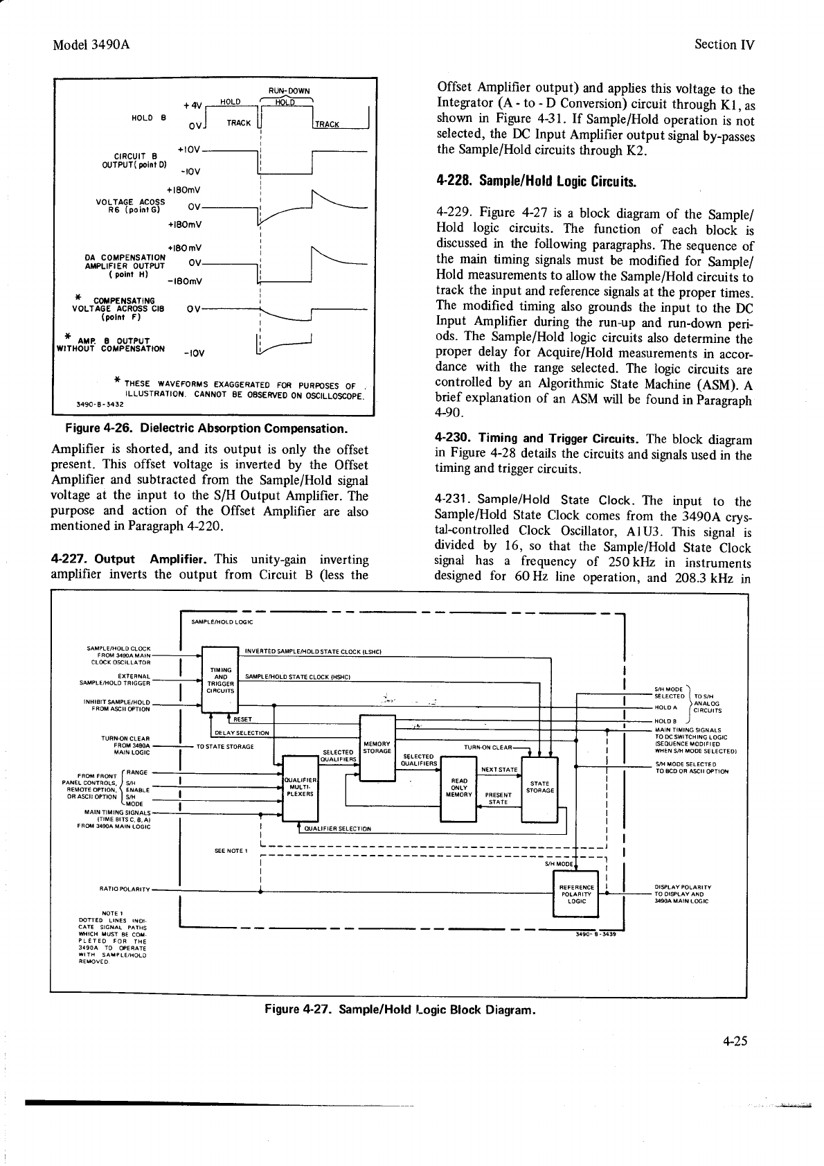
Model3490A
Figure
4-26. Dielectric
Absorption
Compensation.
Amplifier is shorted, and its output is only the offset
present. This offset voltage is inverted by the Offset
Amplifier and subtracted from the Sample/Hold sigral
voltage at the input to the S/H Output Amplifier. The
purposg ald action of the Offset Amplifier are also
mentioned in Paragraph
4-220.
4-227. Output Amplifier. This unity-gain inverting
amplifier inverts the output from Circuit B (less the
Section
IV
Offset Amplifier output) and applies
this voltage to the
Integrator (A - to - D Conversion)
circuit through
Kl, as
shown
in Figure 4-31. If Sample/Hold
operation
is not
selected,
th9 DC Input Amplifier output signal
by-passes
the Sample/Hold
circuits through K2.
4-228.
Sample/Hold
Logic Circuits.
4-229. Fipre 44,7 is a block diagram
of the Sample/
Hold logic circuits. The function of each block is
discussed
in the following paragraphs.
The sequence
of
the main timing signals
must be modified for Sample/
Hold measurements
to allow the Sample/Hold circuits
to
track the input and
reference
signals
at the proper times.
The modified timing also grounds the input to the DC
Input Amplifier during the run-up and run-down peri-
ods. The Sample/Hold logic circuits also determine the
proper delay for Acquire/Hold measurements
in accor-
dance with the range selected.
The logic circuits are
controlled by an Algorithmic State Machine (ASM). A
brief explanation of an ASM will be found in paragraph
4-90.
4-290. Timing and Trigger
Circuits. The block diagam
in Figure
4-28 details
the circuits
and
sigrals
used
in the
timing and trigger circuits.
4-231.
Sample/Hold
State Clock. The input to the
Sample/Hold
State
Clock comes
from the 34904 crvs-
tal-controlled Clock Oscillator, A1U3. This signal is
divided by 16, so that the Sample/Hold
State Clock
sigral has a frequency of 250 kHz in instruments
desigred for 60 Hz line operation,
and 208.3
kHz in
+4V
HOLO 8 OV
crRcurr B +lov
OUTPUT( ooint
O)
' -tov
+t8OmV
VOLTAGE ACOSS
R5
(poinr
G) ev
+l80mv
+l8Omv
oa coMPENsATtoN ^.,
AMPLIFIER OUTPUT VY
( Dolnl H)
" -l8OmV
* coupeNsaltlc
VOLTAGE ACROsS
CIO
(polnr F)
* lye e outpur
WITHOUT
COTPENSATION
OV
* TxEsE
wav€FoRMs
EXAGGERATEo
FoR
puRposEs
oF
ILLUSTRATION.
CANNOT
8E
OSSEFr'ED
ON OSCILLOSCOPE
1490-8-3432
SAMPLE/AOLD CL@K
FFOM
g$A MAIN
CL@K O$ILLATOR
EXTEiNAL
SMPLE/HOLO
TRIGGEA
INHIAIT
$MPLE/HOLD
FFW A$II @TION
TURN.ON
CLEAF
FROM
g9OA
MAIN
LGIC
r*m r"orr [ "A^G€
PANET CONTROLS,
,/ S
F€MOI€ OPTION. \ ENAALE
oa asl OpTtoN I gH
\MODE
MAIN
TIMING
SIGNALS
{TrME BtTSC,8,A)
FRil 34SA MAIN
LOGIC
I
I
- IO STATE STOAAGE
yr uooe )
sELEcrEo
I Tos/H
HoLo
a /äl$t?,".
I
NOLD A '
MAIN TIMING
SIGNALS
TO
E SWITCHING
IOGIC
(SOU€NCE
MODIFIEO
WH€N
Sß MOOE
SEIECTEDI
S MOOE
S€LECTEO
TO rcO OR N[ @Trfr
ßATIO rcLARITY
NOTE I
@nEo LrNES r{Or.
CATE SIGNAI PAGS
wtcH uusT BE Cq.
PL
E TEO FOR THE
3490A TO EERATE
WITA SAIPIEAOLO
iErcV€D
OISLAY POLAFITY
IO OI$LAY ANO
g9OA MAIN LGIC
Flgure
4-27. Sample/Hold
Logic Block Diagram.
+25
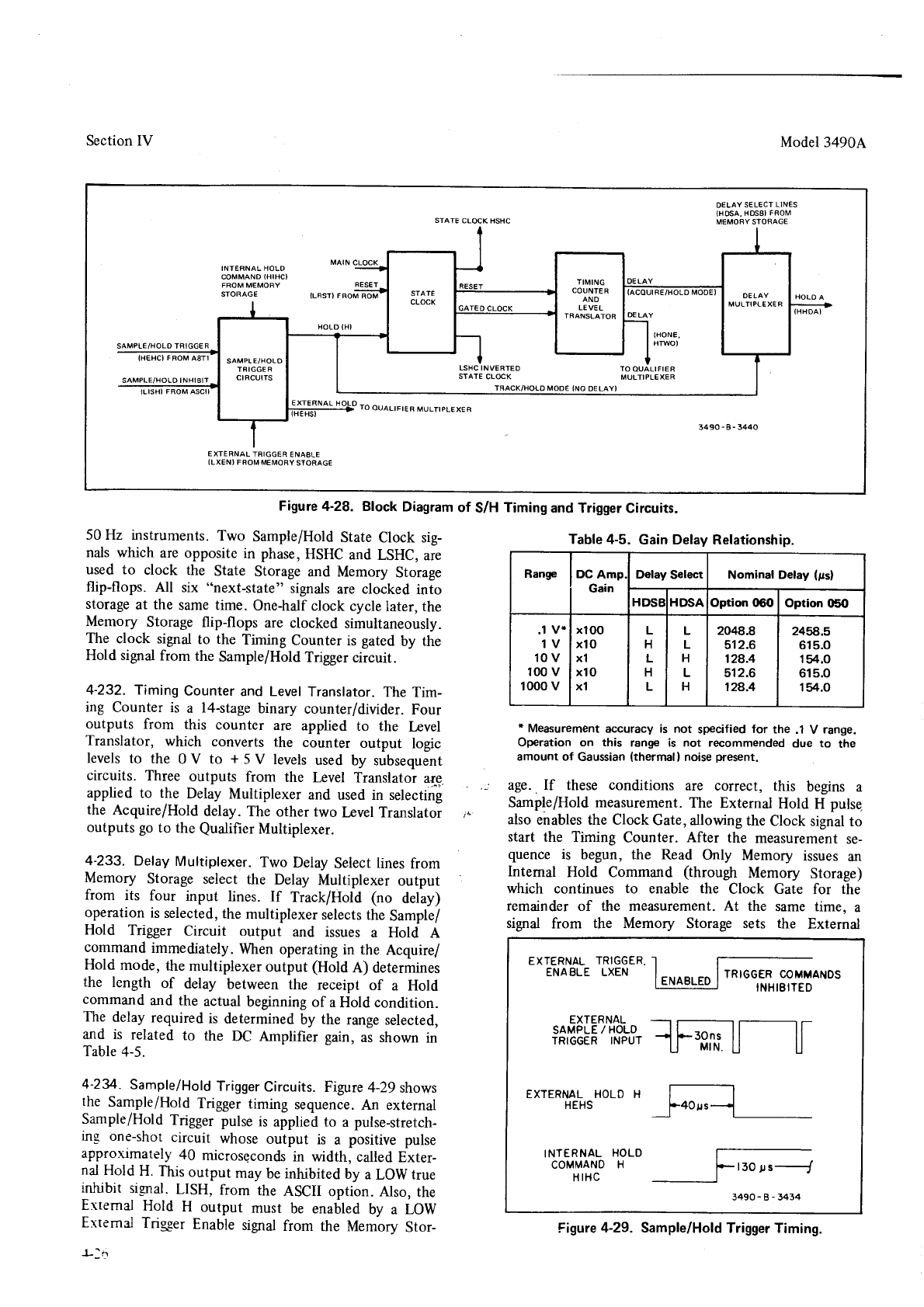
Section IV
50 Hz instruments.
Two Sample/Hold
State Clock sig-
nals which are
opposite in phase,
HSHC
and
LSHC,
are
used to clock the State Storage
and Memory Storage
flip-flops. All six "next-state" signals
are clocked into
storage
at the same time. One-half
clock cycle
later, the
Memory Storage flip-flops are clocked simultaneously.
The clock signal
to the Timing Counter is gated
by the
Hold sigral from the Sample/Hold
Trigger
circuit.
4-232. Timing
Counter
and Level
Translator.
The Tim-
ing Counter is a l4-stage
binary counter/divider.
Four
outputs from this counter are applied to the kvel
Translator, which converts the counter output logic
levels
to the 0 V to + 5 V levels
used by subsequent
circuits. Three outputs from the trvel Translator
arg.
applied
to the Delay Multiplexer and used in selecting
the Acquire/Hold
delay. The other two kvel Translator
outputs go
to the Qualifier
Multiplexer.
4-233. Delay
Multiplexer. Two Delay
Select
lines
from
Memory Storage
select the Delay Multiplexer output
from its four input lines. If Track/Hold (no delay)
operation
is selected,
the
multiplexer
selects
the
Sample/
Hold Trigger Circuit output and issues
a Hold A
command
immediately.
When
operating
in the Acquire/
Hold mode, the
multiplexer
output (Hold A) determines
the length of delay between the receipt of a Hold
command
and the actual
beginning
of a Hold condition.
The delay
required
is determined
by the range selected,
and is related to the DC Amplifier gain, as shown in
Table
4-5.
4-23. Sample/Hold
Trigger
Circuits.
Figure
4-29
shows
the Sample/Hold
Trigger
timing sequence.
An external
Sample/Hold
Trigger
pulse
is applied to a pulse-stretch-
ing one-shot
circuit whose
output is a positive pulse
approx-rmately
40 microsqconds
in width, called
Exter-
nal
Hold H. This
output may
be inhibited
by a
LOW
true
inhibit sigral. LISH, from the ASCII option. Also, the
Ertemal Hold H output must be enabled
by a LOW
Ertemal Triaeer
Enable
signal
from the Mem'ory
Stor-
l-'h
Model3490A
* Measurement accuracy is not specified for the .1 V range.
Operation on this range is not recommended due to the
amount of Gaussian
(thermal) noise
present.
age. If these conditions are correct, this begins a
Sample/Hold measurement.
The External
Hold H pulse.
also
enables the Clock
Gate, allowing
the
Clock signal
to
start the Timing Counter. After the measurement
se-
quence is begun, the Read Only Memory issues
an
Internal Hold Command (through Memory Storage)
which continues to enable the Clock Gate for the
remainder of the measurement. At the same time, a
sigral from the Memory Storage sets the External
STATE
CLOCK
HSHC
DELAY SELECT LINES
IHOSA, HDSEI FROM
MEMORY STORAGE
SAMPL€/HOLD TRIGGER
IHEHCI FROM
llrsHt FRoM
ascrl
EXTEfrNAL TO
OUALIFIER
MULTIPLEXER
1490-8-3440
EXTERNAL TBIGGER
ENASLE
(LXEN} FROM MEMORY STORAGE
LSHC INVERTED TO OUALIFIEF
STATE CLOCK MULTIPLEXER
Figure
4-28. Block
Diagram
of S/H Timing
and
Trigger Circuits.
Table
4-5. Gain Delay Relationship.
Range DC
Amp
Gain Delay Select Nominal Delay (psl
HDSEHDSA Option 060 Option 05t0
,1
V.
1V
10v
100 v
1000 v
xlOO
xlO
xl
xlO
xl
L
H
L
H
L
L
L
H
L
H
2048.8
512.6
128.4
512.6
124.4
2458.5
615.0
154"0
615.0
154.O
EXTERNAL
TRIGGER,
ENABLE LXEN
EXTERNAL
;s,t3i5'/rp,ly,ffi
EXTERML HOLD H
HEHS
I NTERNAL
COMMAND
H
IHC
HOLD
H
TRIGGER COMMANDS
INHIBITED
l3O
rs--J
Figure
4-29. Sample/Hold
Trigger Timing.
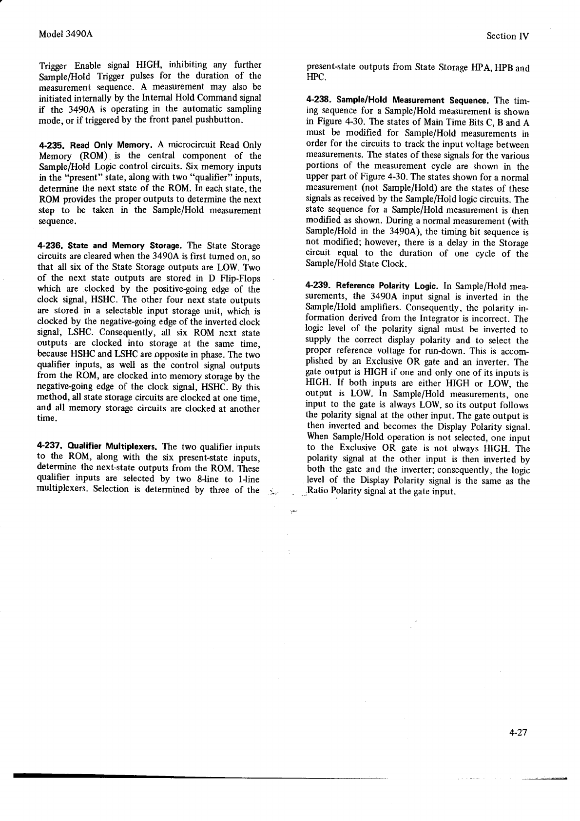
Model3490A
Trigger Enable signal HIGH, inhibiting any further
Sample/Hold Trigger pulses for the duration of the
measurement sequence.
A measurement may also be
initiated internally by the Intemal Hold Command signal
if the 3490A is operating in the automatic sampling
mode, or if triggered
by the front panel pushbutton.
+235. Read
Only Memory. A microcircuit
Read
Only
Memory (ROM) is the central component of the
Sample/Hold Logic control circuits. Six memory inputs
in the "present" state, along with two "qualifier" inputs,
determine the next state of the ROM. In each
state, the
ROM provides the proper outputs to determine the next
step to be taken in the Sample/Hold measurement
sequence.
+236. State and Memory Storage. The State Storage
circuits are
cleared
when the 3490A is first tumed on. so
that all six of the State Storage outputs are LOW. Two
of the next state outputs are stored in D Flip-Flops
which are clocked by the positive-going edge of the
clock signal, HSHC. The other four next state outputs
are stored in a selectable
input storage
unit, which is
clocked
by the negative-going
edge
ofthe inverted
clock
sigral, LSHC. Consequently,
all six ROM next state
outputs are clocked into storage at the same time,
because HSHC
and LSHC are
opposite in phase.
The two
qualifier inputs, as well as the control signal outputs
from the ROM, are clocked into memory storage
by the
negative-going
edge of the clock signal, HSHC. By this
method, all state
storage
circuits are clocked at one
time,
and all memory storage
circuits are clocked at another
time.
4-23!. Oualifier Multiplexers. The two qualifier inputs
t9 the ROM, along with the six present-state
inputs,
determine the next-state
outputs from the ROM. These
qualifier inputs are selected by two 8line to lline
multiplexers. Selection is determined bv three of the
Section
IV
present-state
outputs from State Storage FIPA,
HpB and
HPC.
ut-238.
Sample/Hold
Measurement
Sequence. The tim-
ing sequence
for a Sample/Hold
measurement
is shown
in Figure 4-30. The states
of Main Time Bits C, B and A
must be modified for Sample/Hold measurements
in
order for the circuits to track the input voltage between
measurements.
The states
of these signals
for the various
portions of the measurement
cycle are shown in the
upper part of Figure
4-30.
The states shown
for a normal
measurement
(not Sample/Hold) are the states
of these
signals
as
received
by the Sample/Hold
logic circuits. The
state sequence
for a Sample/Hold
measurement
is then
modified as shown. During a normal measurement (with
Sample/Hold in the 3490A), the timing bit sequence
is
not modified; however, there is a delay in the Storage
circuit equal to the duration of one cycle of the
Sample/Hold
State Clock.
zl-239.
Reference
Polarity Logic. In Sample/Hold
mea-
surements, the 3490A input signal is inverted in the
Sample/Hold
amplifiers.
Consequently,
the polarity in-
formation derived from the Integrator is incorrect. The
logic level of the polarity signal must be inverted to
supply the correct display polarity and to select the
proper reference voltage for run-down. This is accom-
plished by an Exclusive OR gate and an inverter. The
gate
output is HIGH if one and only one
of its inputs
is
HIGH. If both inputs are either HIGH or LOW, the
output is LOW. In Sample/Hold
measurements,
one
input to the gate
is always
LOW, so its output follows
the polarity signal
at the other input. The gate
output is
then inverted
and becomes the Display
Polarity signal.
When
Sample/Hold
operation
is not selected,
one input
to the Exclusive
OR gate is not always HIGH. The
polarity signal at the other input is then inverted by
both the gate
and the inverter;
consequently,
the logic
level of the Display Polarity signal is the same as the
..Ratio
Polarity
signal
at the gate
input.
4-27
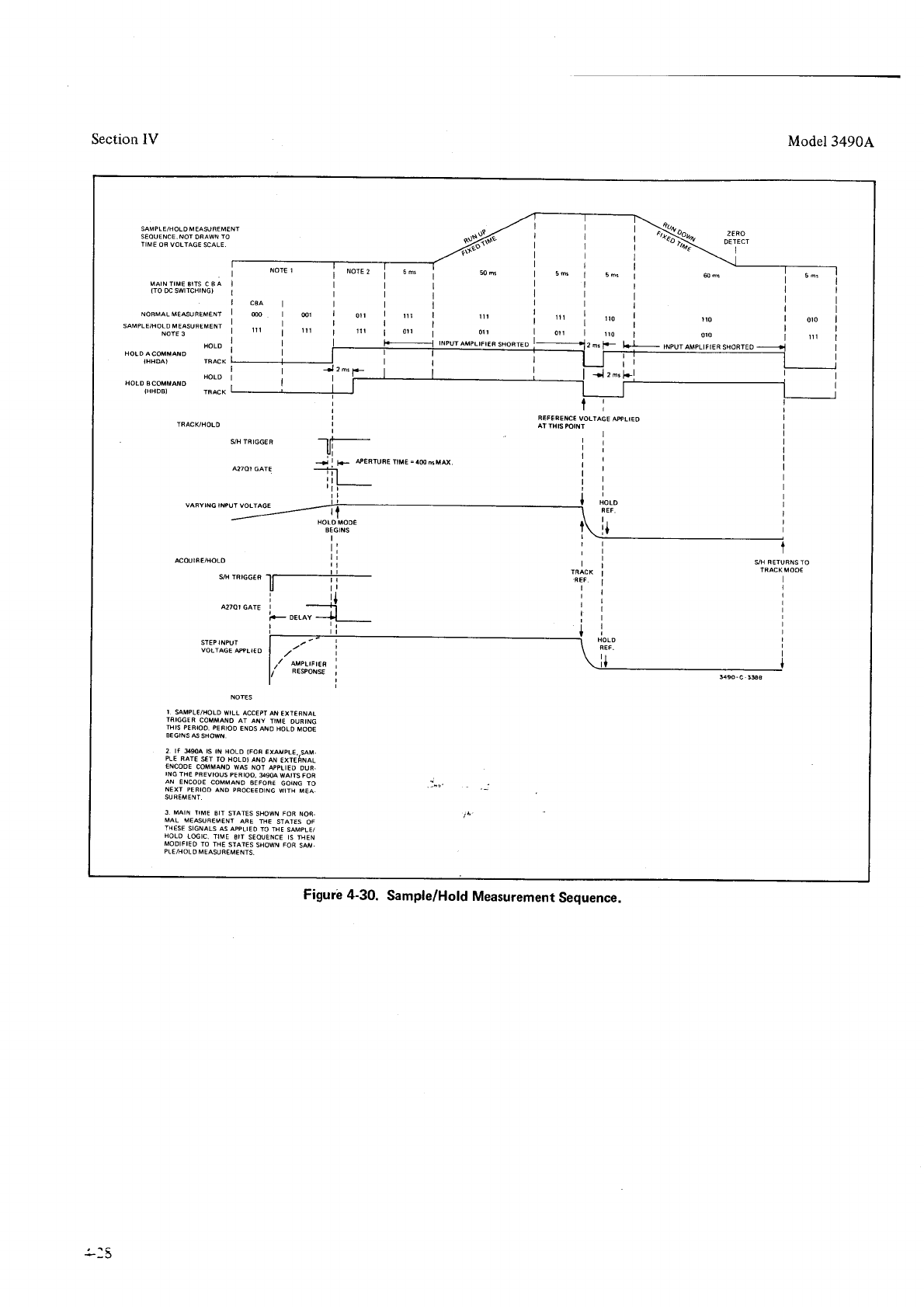
Section IV Model3490A
SAMPLE/HOLD MEASUNEMENl
SEOUENC€. NOT
OFAWN
TO
TIME
Oß VOLTAGE
SCA!E.
MAIN
TIME BITS C 8A
{TO
N SWrrCHrNG)
NOBMAL MESUßEü€NT
SAMPLE/HOLD MEASUßEMENT
NOTE
3
HOLO
HOLDACOMMANO
IHHDAI TRÄCX
c8a
@
11i
011
il!
IO
il0
r10
0r0
0t0
111
INPUI
AMPLIFI€R
SHORTEO Ll-- rrpur
lueuFrER sHoRTEo
I
HOLD BCOMMAND
IHHDBI
IRACK/HOLD
9H IRIGGER
42701 GATE
VAAYING INPUT
VOLTAGE
I
I
-F--
ill
Ul
--j i s +enrune rlME=4mBüAX
R€F!RErcE VOLTAGE
MLIED
AT THIS
POINT
STEP INPUT
NOr€S
RESPONSE
HOLD
FEF.
ll
It
*$-c-3$a
r SAMPLE/HOLD
WILL ACCEPf
AN
EXTEFNAT
TRIGGER
COMMANO
AT ANY TIME DURING
THIS PERIOO.
PEFIOD
ENOS
ANO HOLD
MOOE
BEGINS
N SHOWN.
2. tf g$a rs t( HoLD tFoß €XAMPL€,
SAM.
pLE FATE
s€T To aoLD' aND aN ExTEANAL
ENCODE COMMAND WAS NOT APPIIEO DUR-
rNG
TH€ PBEVTOUS
pERlOO.
A9OA WAtS aO8
AN ENCOOE
COMMANO
SEFOBE
GOING TO
NEXT PERIOO
AND PfiOCEEDING
WITH MEA.
SUREMENT.
3, MAIN TIME SIT STATES
SHOWN
FOR
NOA.
MAL MEASUFEMENT
ARE THE STAfES OF
TXES€
SIGNALS
AS APPLIEO
TO THE
SAMPLE/
HOLO L@IC. TIME 8IT SE@ENCE IS THEN
MODIFIEO
IO THE
SfATES
SHOWN FOR
SAM,
PL€/HOIO
MEASUR€MENTS.
ortoroo.,
I J
l- oruY --Jl
; ri--
Figurb 4-30. Sample/Hold
Measurement
Sequence.
j-tE
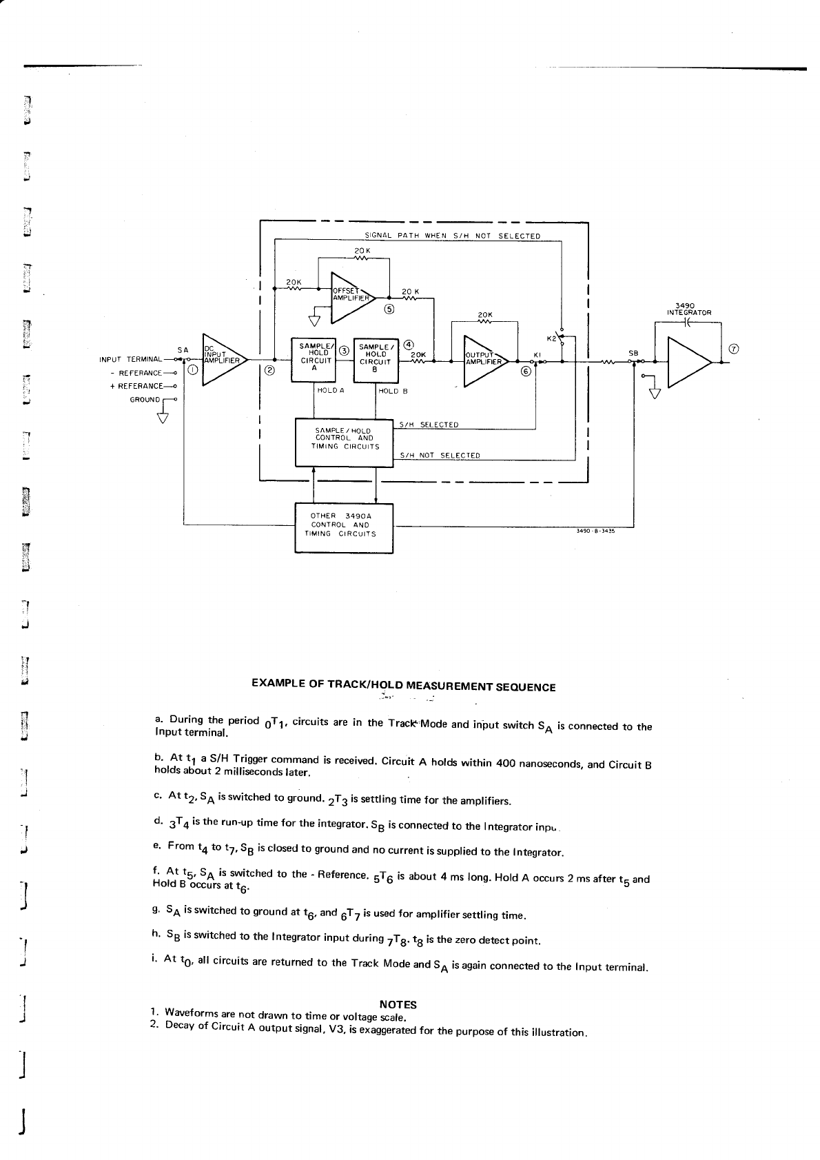
I
./
;'
I
!:
-J
tfr
ii
,:t
,a
:i
t
.=!
rt
*{
;it,;
ii
i
:r
.:
J
S
GNAL
PATH /H NOT SELECTED
EXAMPLE OF TRACK/HOLD MEA-SUREMENT
SEOUENCE
a' During the period 6T1, circuits are in the Tract+,Mode
and in'put switch SA is connected to the
lnput terminal.
P' .f'1r a S/H T-rigger
command is received.
Circuit A holds within 400 nanoseconds,
and Circuit B
holds about 2 milliseconds
later.
c. At t2, 54 is switched to ground. 2T3 is
settling time for the amplifiers.
d' 3To is the run-up time for the integrator. sg is
connected to the I ntegrator inpu.
e' From t4to t7,sg is crosetJ
to ground and no current is
suppried
to the Integrator.
f' At t5, s4 is switched to the - Reference.
5T6 is about 4 ms long. Hold A occurs 2 ms after t5 and
Hold B occurs at t6.
9. 54 is
switched to ground at t6, and 6T7 is used
for amplifier settling time.
h' sg is
switched to the lntegrator input during 7Tg. tg is the zero detect point.
i' At t0, all circuits are returned to the Track Mode and s4 is again
connected to the lnput terminal.
Waveforms
are
not
drawn
to time
o, "o,,rn"
I?[lt
Decay
of circuit A output signal,
v3, is eägger;d for the purpose
of this iilustration.
3490
INTEGRATOR
*
ai
j
:J
,l
'f
I
I
1.
INPUT
TERMINAL
- REFERANCE<
+ REFERANCEJ
GRouN0 T{
I
V
OTHER 349OA
CONTROL ANO
TIMING
CIRCUITS
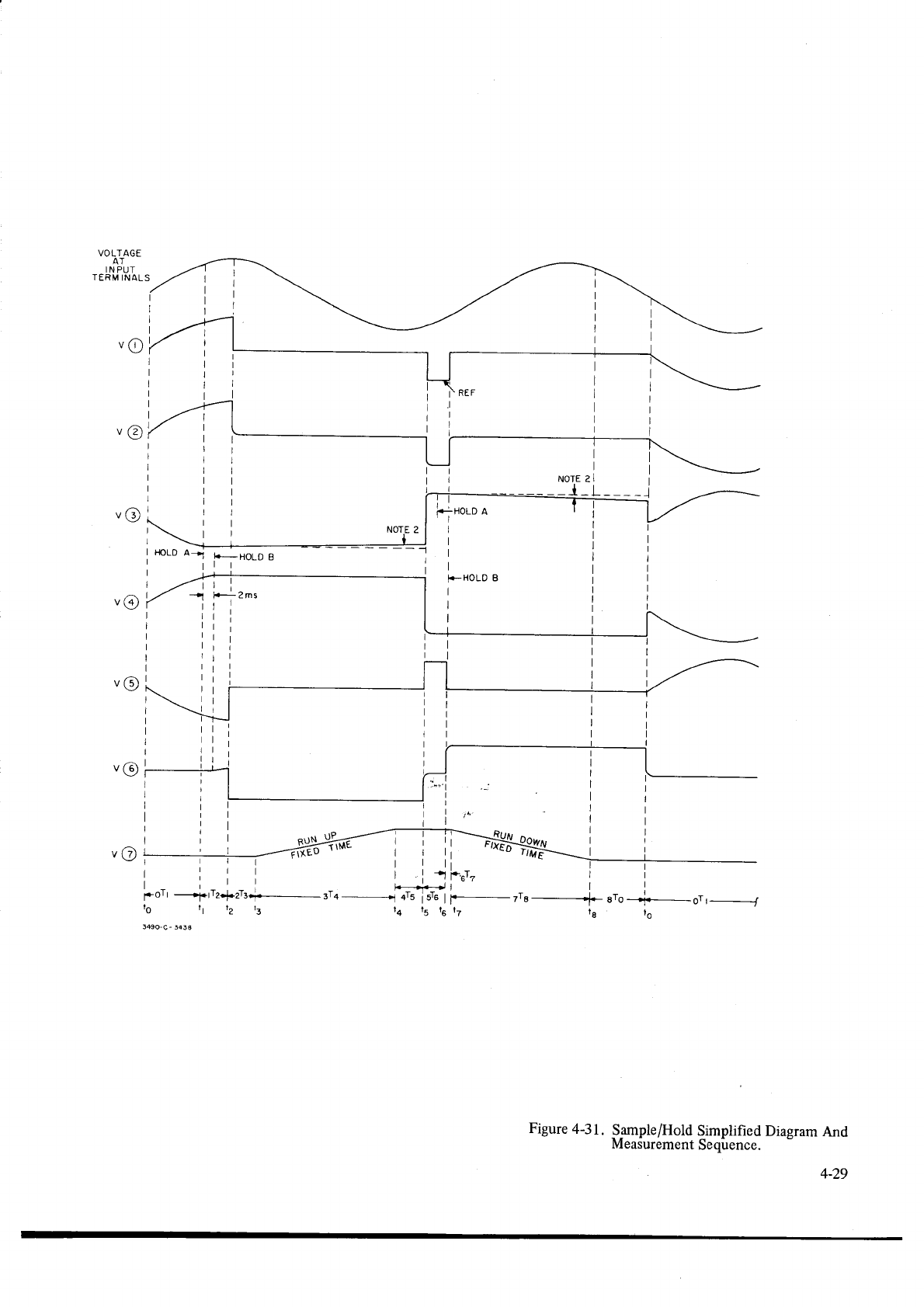
NOTE 2 I
rIOLD
A1 b_HOLD B
rll
| - ;- l_ i h---l*--r i"' I I
gort ----+prr2{zrs.i*-- 3r4
------+ qrs
I
sre
I
l.-- zra
-----f ero
-+-- or r
-_____-
tO tt t2 t3 t4 t5 t6 ll l8 tO
Figure
4-31. Sample/Hold
Simplified
Diaeram
And
MeaSurement
Seqüence.
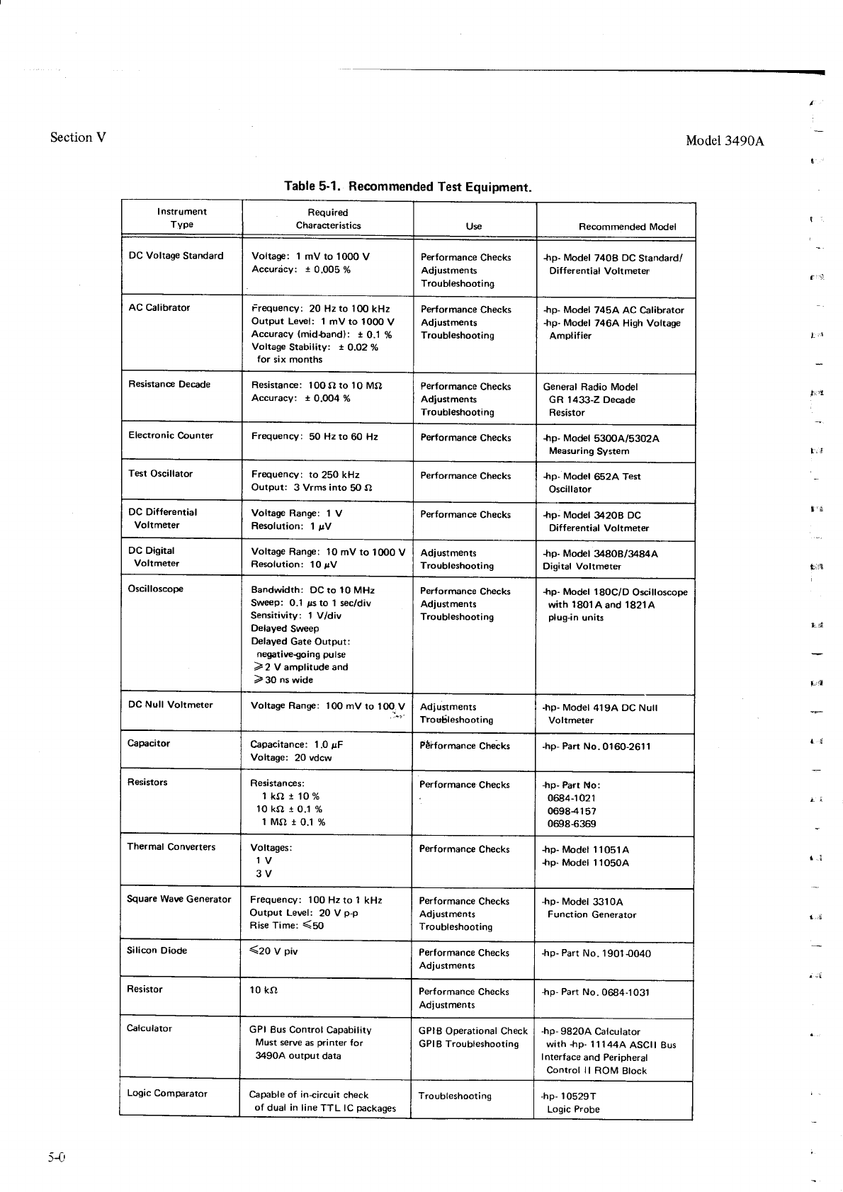
Section V Model 34904
Table
5-1. Recommended
Test
Equipment.
I
nstrument
Type Required
Characteristics Use Recommended Model
DC Voltage Standard Voltage: I mV to 1000
V
Accuräcy: 1 0.005 %
Performance
Checks
Adiustments
Troubleshooting
+rp- Model
7408 DC
Standard/
Differential
Voltmeter
AC Calibrator Frequency:
20 Hz
to 1OO
kHz
Output Level: 1 mV to 10OO
V
Accuracy
(midlcand): r 0.1
%
Voftage
Stability: ! O,O2"Ä
for six months
Performance
Checks
Adiustments
Troubleshooting
tro- Model
745A AC Calibratol
-trp-
Model
7464 High Voltage
Amplif
ier
Resistance Decade Resistane: 100
A to 1O Mtr,
Accuracv: i 0.004 % Performance
Checks
Adiustments
Troubleshooting
General
Radio Model
GR 1433-2 Decade
Resistor
Electronic Counter Frequenry: 50 Hz to 60 Hz Performance
Checks {rp- Model 53OOA/5302A
Measuring
System
Test Oscillator Frequency: to 25O kHz
Output: 3 Vrms into 50 s,
Performance Checks +rp-
Model 6524 Test
Oscillator
DC Differential
Voltmeter
Voltage Range: 1 V
Resolution: 1 rrV
Performance
Checks +rp- Model
34208 DC
Difterential
Voltmeter
DC Digital
Voltmeter
Voltage Range: 10 mV to 1
OO0 V
Resolution: 10
//V
Adlustments
Troubleshooting *rp- Modet 34808/3484A
Digital Voltmeter
Oscilloscope Bandwidth: DC to 10 MHz
Sweep: 0.1 ,is to 1 sec/div
Sensitivity: 1 V/div
Delayed Sweep
Delayed Gate Output:
negative-going pulse
>2Vamplitudeand
> 30 ns
wide
Performance
Checks
Adiustments
Troubleshooting
+rp-
Mod€l 18OC/D
Orcilloscope
with 1
8O1 A and
1
821
A
plugin units
DC Null Voltmeter Voltage
Range: 100
mV ro lOO
V Adiustments
Tlou6leshooting
-hp-
Model
419A DC Null
Voltmeter
Capacitor Capacitance: 1.0 pF
Voltage: 20 vdcw
Päiformance Checks +rp- Part
No.
01 60-261
I
Resistors Resistanc€s:
1
ka i 10 %
lokf,} 10.1
%
1Mf,,rO.1
70
Performance Checks +rp- Part
No:
0684-r 02 l
06984157
0698.6369
Thermal
Converters Voltages:
1V
3V
Performance Checks +rp- Model 1'l051A
+lp-
Model 11O5OA
Square Wave Generator Frequency: 100
Hz to 1
kHz
Output Level: 20 V p-p
Rise
Time:
(50
Performance
Checks
Adiustments
Troubleshooting
+p- Model
3310A
Function
Generator
Silicon Diode (20 v piv Performance Checks
Adiustments
+rp- Part
No. 1
901 {040
Resistor 10 kn Performance Checks
Adlustments
+|p- Part No.0684-1031
C€lcu lator GPI 8us Control
Capabilitv
Must serve
as
printer
for
34904 output
data
GPIB Ooerational Check
GPI
B Troubleshooting
-hp-
9820A Calculator
with fip- 11144A
ASCII Bus
I nterface and Perioheral
Control ll ROM Block
Logic Comparator Capable of in+ircuit check
of dual in line TTL lC packages
Troubleshooting -hp-
105297
Logic
Probe
t:il:
t .:l
tE
Äi
5-C,
Model34904 Section V
5-r.
TNTB0DUCTIoN.
5-2. This section contains
performance
tests
and adjust-
ment procedures
for the Model 3490A Multimeter. The
performance
tests determine
whether
your instrument is
operating within its published
specifications.
The adjust-
ment procedures are
provided to help you maintain your
instrument within specification
limits.
5.3.
RECOMMENDED TEST
EOUIPMENT.
54. Test equipment required for the performance
tests
and adjustment procedures
is listed in Table 5-l . Any
equipment that satisfies
the critical specifications
given
in the table may be substituted for the recommended
model.
5.5. TEST RECOBD.
5-6. A Performance
Test Record
is provided
at the end
of this section for the purpose
ofrecording the results of
the Performance
Tests.
This record lists all of the tested
specifications and their acceptable
limits. This record
can be removed from the manual and retained as a
permanent
record
of the incoming inspection or routine
maintenance performed on the instrument. This record
may be reproduced for your use without special permis-
sion.
SECTION
V
MAI NTENAN CE
PERFORMANCE
CHECKS
S7.
PERFORMANCE
TESTS.
5-8. Use the following test procedures to determine
whether your instrument is opefating within its pub-
lished specifications.
The test limits given
in the accur-
acy tests and on the performance test record compare
the instrument to the 90-day specifications given in
Table l-l . However,
if your accuracy requirements are
met by other specifications, such as the 30-day or
Gmonth specifications,
the test limits should
be adjusted
accordingly. The performance
of the instrument should
be tested upon receipt and at regular intervals deter-
mined by your accuracy
requirements. Refer also
to Mil.
Spec. MIL{45662A.If the 3490A fails to meet one or
more of its specifications, refer to the Adjustment
Procedures,
Paragraph
5-51. The 3490A and test equip-
ment should
be operated
ät normal line voltage with the
3490A rear panel line selector
switches set
as
instructed
in Figure 2-1. Allow at least one hour warm-up time for
the 3490A before beginning
the following tests.
$9. DC
VOLTMETER
ACCURACY
TEST.
5-10. A dc voltage
standard
(-hp-
7a0B) is required for
this
test.
Connect Guard to Input Low or damage
to
the instrument may result.
a. Set 3490A FUNCTION to DC, RANGE to .l V.
b. Connect
dc standard
between
INPUT HIGH and
LOW terminals.
c. Select 3490A ranges
and dc standard
positive
and
negative
outputs listed in Table 5-2. Display should be
within limits shown in each case.
$11. AC
VOLTMETER
ACCURACYTESTS.
5-l
2. Because
of the
voltage range
and bandwidth of the
3490A ac voltmeter
circuits, more than
one
test setup is
required to verify the accuracy specifications. The -hp
Model
745A/746A AC Calibrator may be used
to check
the accuracy of all ranges
at frequencies up.to I l0 kHz;
however,
the accuracy of this sigral source alone in some
cases
may not be great
enough to ensure a valid test of
Table
5-2. DC
Voltmeter Accuracy.
3490A
Range DC Standard
Output Display Limits
.1 V
1V
10v
100 v
1000
v
r 0.010O0
V
r 0.05000
V
r 0.10000
V
t o.10000 v
r 0.50000 V
r 1.00000 v
1
1.00000 V
i 10.0000 v
1
10.0000
V
r 100.000
V
I 100.000
v
i 500.000 v
r+
1000.00 v
t .009995 to .010OO5
V
l .049990
to .050010 V
t .099985 to .10001 5 V
I 0.09997 to O.10003 V
I 0.49994 to 0.50006 V
r 0.99990 to 1
.0001O
V
! 00.9997 to 01 .Oq)3 V
t 09.9990 to 10.0010 V
t 009.997
to 010.003
V
t 099.990 to 10O.O10
V
10099.97
to 010O.O3 V
r 0499.92 to 0500.08 V
+
(x199.86
to 1000.14 V
* lf -hp- 7408 DC Standard is used, do not apply negative
voltage
greater
than - 500 V.
5-l
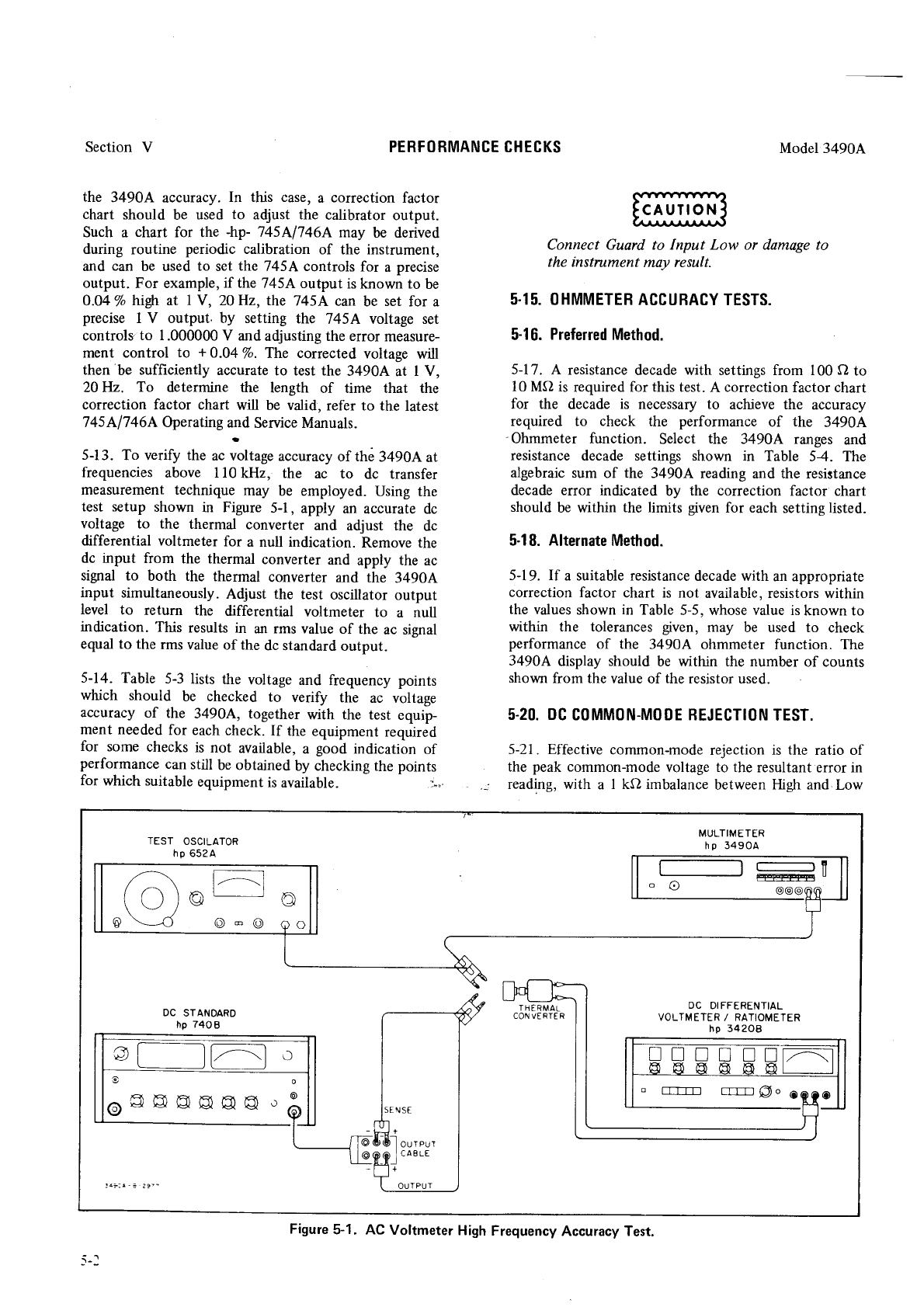
Section V
the 3490A accuracy.
In this case,
a correction
factor
chart should be used to adjust the calibrator
output.
Such a chart for the -hp- '745A1746A
may be derived
during routine periodic calibration of the instrument,
and can be used
to set
the 745A controls
for a precise
output. For example,
if the
745A output is known to be
0.04% high at I V, 20H2, the 745A can
be set for a
precise 1 V output. by setting the 745A voltage set
controls'to 1.000000
V and
adjusting the error
measure-
ment control to +0.04%. The corrected
voltage will
then be sufficiently accurate
to test the 3490A at I V,
20H2. To determine the length of time that the
correction factor chart will be valid, refer to the latest
745A1746A Operating
and
Service Manuals.
t.
5-13. To verify the ac voltage
accuracy
of the 34904 at
frequencies above I l0 kHz, the ac to dc transfer
measurement technique
may be employed. Using the
test setup shown in Figure 5-1, apply an accurate dc
voltage to the thermal converter and adjust the dc
differential voltmeter for a null indication. Remove the
dc input from the thermal converter and apply the ac
signal to both the thermal converter and the 349OA
input simultaneously.
Adjust the test oscillator
output
level to return the differential voltmeter to a null
indication. This results in an rms value of the ac signal
equal to the rms value
of the dc standard
output.
5-14. Table 5-3 lists the voltage
and frequency
points
which should be checked to verify the ac voltage
accuracy of the 349OA, together with the test equip-
ment needed
for each check.
If the equipment
required
for some
checks
is not available,
a good indication of
performance
can
still be obtained
by checking the points
for which suitable
equipment
is available. r-..
Model3490A
Connect Guard to Input Low or damage
to
the instrument may result.
5.15.
OHMMETER
ACCURACY TESTS.
5-l
6. Preferred
Method.
5-17. A resistance
decade with settings from 100Oto
10
MO is required for this test.
A correction
factor chart
for the decade is necessary
to achieve the accuracy
required to check the performance of the 34904
'Ohmmeter function. Select the 3490A ranges and
resistance
decade settings shown in Table 54. The
algebraic sum of the 34904 reading and the resistance
decade error indicated by the correction factor chart
should be within the limits given for each
setting
listed.
5-l
8. Alternate
Method.
5-19. If a suitable resistance
decade with an appropriate
correction
factor chart is not available, resistors
within
the values
shown
in Table
5-5, whose value is
known to
within the tolerances given, may be used to check
performance
of the 3490A ohmmeter function. The
3490A display should be within the number
of counts
shown
from the
value of the resistor used.
5.20. DC
COMMON-MODE REJECTION
TEST.
5-21. Effective
common-mode
rejection is the ratio of
the peak
common-mode
voltage
to the
resultant error in
PERFORMANCE CHECKS
t-,,,-----l
(O
)@u o
@\:d o-o oo
MULTIMETER
hp 34904
o@oo@
DC OIFFERENTIAL
VOLTMETER
/ RATIOMETER
hp 542O8
OU
T
PUT
CAELE
Figure
5-1. AC
Voltmeter
High
Frequency
Accuracy Test.
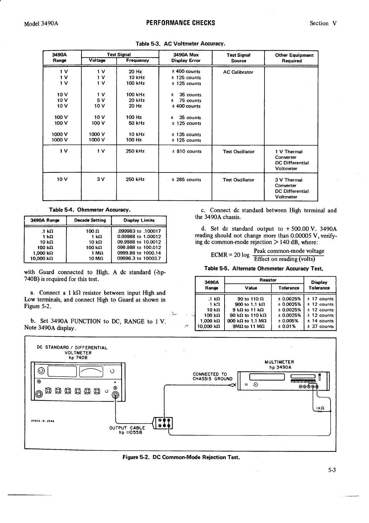
Model
34904 PERFOBMANCE
CHECKS Section V
c. Connect dc standard between Higfr terminal and
the 3490A chassis.
d. Set dc standard
output to + 500.00
V. 3490A
reading
should not change
more than 0.00005 V, verify-
ing
dc
common-mode
rejection > 140 dB,
where:
Peak
common-mode
voltage
ECMR
= 20log
" Effect on reading
(volts)
with Guard connected to High. A dc standard
(-hp-
7zt0B) is
required for this
test.
a. Connect
a I kQ resistor
between
input High
and
Low terminals,
and connect High to Guard as
shown
in
Figure
5-2.
b. Set
3490A
FUNCTION to DC.
RANGE to I V.
Note
3490A
display.
Table 5-3. AC Voltmeter
AccuracY.
3490A
Range Test Sisnal 3490A Max
Display Error Test Signal
Source
Other Equipment
Required
voltago Frequency
1V
1V
1V
10v
10v
10v
100
v
100
v
1000
v
1000
v
1V
1V
1V
1V
5V
10v
10v
100 v
1000 v
1m0 v
2Q
Hz
10
kHz
100 kHz
100
kHz
2O
kHz
2Q
Hz
100
Hz
50
kHz
1O kHz
100 Hz
t 400 counts
t 125 counts
r 125 counts
t 35 counts
t 75 counts
t 40O counts
t 35 counts
t 125 counts
t 135 counts
r 125 counts
AC Calibrator
1V 1V 25O
kHz * 810 counts Test Oscillator 1 V Thermal
Converter
DC Differential
Voltmeter
10v 3V 25O kHz t 285 counts Test Oscillator 3 V Thernul
Converter
DC Differential
Voltmeter
Table
54. Ohmmeter Accuracy.
39OA Rang Docade Sotting Display Limits
.1
ko
lkn
10
ks}
100 ko
1,Oq)
ka
10,000 ko
100 sr
1ks}
10
kn
100
ka
lMO
10
MO
.099983 to .100017
0.99988 to 1.00012
09.9988
to 10.OO12
099.988 to 1O0.012
0!X,9.86 to 1000.14
09996.3 to 10003.7
Table
5€. Alternate
Ohmmeter Accuracy Test.
3490A
Range
Resistor Display
ToleranceValue Toleranca
.1 ko
1k:)
10
ko
1OO
ko
1,000 ko
10,000 ks)
90to
110o
90O
to 1.1 ko
9koto11
ksl
90kOto110kO
90O
ko to 1.1
Msl
gMf}to
11MO
t o.oo25%
r 0.0025%
t O.OO25%
r 0.0025%
r 0.005%
r 0.01%
t 17 counts
t 1 2 counts
t 12 counts
t 12 counts
* 14 counts
I 37 counts
DC STANDARO
/ DIFFERENTIAL
VOLTMETER
hp 74OB
eEo@oo
OUTPUT
CAELE
ho llO55B
5490Ä -a - 29a!
Figure 5-2. DC Gommon-Mode Rejeaion
Test.
5-3
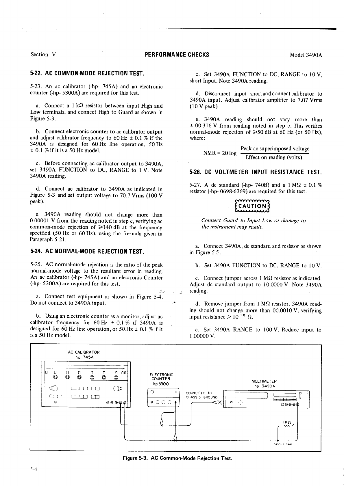
Section V
5.22.
AC
COMMON.MODE
REJECTION
TEST.
5-23. An ac calibrator (hp- 7a5A) and an electronic
counter (-hp-
53004) are required for this
test.
a. Connect a I kCl resistor
between
input High and
Iow terminals, and connect High to Guard as sfiown in
Figure
5-3.
b. Connect electronic counter
to ac
calibrator
output
and adjust calibrator frequency
to 60 Hz t O.l % if the
349OA is desigred for 60 Hz line operation, 50
Hz
! 0.1
%
if it is a 50
Hz model.
c. Before connecting
ac calibrator
output to 3490A,
set 3490A FLJNCTION
to DC. RANGE to I V. Note
3490A reading.
d. Connect ac calibrator to 3490A as
indicated
in
Figure 5-3 and set output voltage
to 70.7 Vrms (100 V
peak).
e. 3490A reading should not change more than
0.00001
V from the reading
noted in step
c,
verifying
ac
common-mode rejection of 2140 dB at the frequency
specified
(50 Hz or 60 Hz), using the formula given
in
Paragraph
5-21.
S24.
AC
NORMAL.MODE
REJECTION
TEST.
5-25. AC normal-mode
rejection is
the
ratio of the peak
normal-mode
voltage
to the resultant error in reading.
An ac calibrator
(-hp-
7454) and an electronic
Counter
(-hp-
5300A) are required
for this
test. ,-..
a. Connect test equipment
as shown in Figure 5-4.
Do not connect
to 3490A input. i^
b- Using
an
electronic counter
as
a monitor,
adjust ac
calibrator frequency for 60 Hz t 0.1
% if 3490A is
designed
for 60
Hz line
operation,
or 50.H2
! O.1
%if it
is a 50
Hz model.
Model
3490A
c. Set 3490A FUNCTION to DC. RANGE to l0 V.
short Input. Note 3490A reading.
d. Disconnect input shortandconnectcalibrator
to
3490A input. Adjust calibrator amplifier to 7.07 Vrms
(10 V peak).
e. 3490A reading should not vary more than
I 00.3
16
V from reading
noted in step c. This
verifies
normal-mode
rejection of )50 dB at 60 Hz (or 50 Hz),
where:
NMR
=
20los Peak
ac superimposed
voltage
Effect on reading
(volts)
5.26.
DC VOLTMETER
INPUT
RESISTANCE TEST.
5-27.
A dc standard
(hp- 7a0B) and a I MA !O.l%
resistor
(-hp-
0698-6369) are required
for this test.
Connect Guard to Input Low or domage to
the instrument may result.
a. Connect
3490A,
dc
standard and
resistor
as
shown
in Figure
5-5.
b. Set 3490A
FUNCTION to DC, RANGE to lOV.
c. Connect
jumper across
I M,fl resistor as indicated.
Adjust
dc standard
output to 10.0000V.
Note 3490A
reading.
d. -Remove
jumper from I MQ resistor. 3490A read-
ing should not change
more than 00.0010
V, verifying
input
resistance
) l0 ro Q.
e. Set 3490A RANGE to 100
V. Reduce input to
1.00000 v.
PEBFORMANCE CHECKS
AC CALIERATOR
hp 7454
ELECTRONIC
COUNTER
hp
53OO MULTIMETER
hp 349O4
CONN€CTEO
1O
CHASSIS
GROUNO r-------l
oQ
I tlr
+T-F++F U
l0 D O 0 0 0 0 00
i@@@@@@
e o@ oo
Figure
5-3. AC Common-Mode
Rejection
Test.
<t
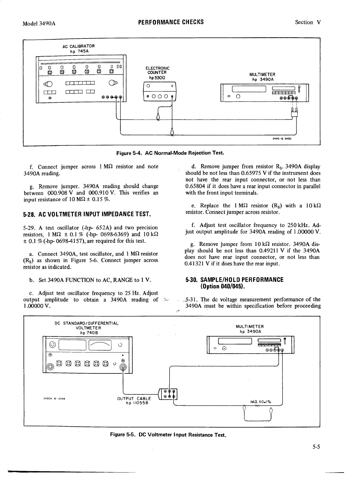
AC CALIBRATOR
hp 7454
nr-rnO0000
ä ö ö ö o o-- ELECTRONIC
COUNTER MULTIMETER
hp53OO hD S49OA
<) rrr-rrr--r] oD
ffi r-r-I-T-'l -T-1
L4 e t".f?
a') o
oooo?
-
\
n
F-
I
5490-B
-y50
Figure
5-4. AC Normal-Mode
Reiection
Test.
Model3490A
f. Connect
jumper across
I MQ resistor and note
3490A reading.
g. Remove jumper. 3490A reading should change
between 000.908V and 000.910V. This verifies an
input resistance
of 10 MQ x O-15
%.
5-28.
AC VOLTMETEH
INPUT IMPEDANCE TEST.
5-29. A test oscillator (-hp 652A) and
two precision
resistors, I MO t O.l % (-hp- 06984369) and l0 kQ
t 0.1 %
(-hp-
06984157),arc required for this test.
a. Connect
3490A, test oscillator, and I Mfl resistor
(\) as shown in Figure 5-6. Connect
jumper across
resistor as
indicated.
b. Set 349OA
FUNCTION to AC, RANGE
to I V.
c. Adjust test oscillator frequency to 25H2. Adjust
output amplitude to obtain a 3490A reading of
1.00000 v.
Section V
d. Remove
jumper from resistor Rs. 3490A display
should
be not less than
0.65975
V if the
instrument
does
not have the rear input connector, or not less than
0.65804 if it does
have a
rear input connector in parallel
with the front input terminals.
e. Replace the l Mfl resistor (R5) with a l0k{-2
resistor. Connect
jumper
across resistor.
f. Adjust test oscillator frequency to 250 kHz. Ad-
just output amplitude for 3490A reading of 1.00000
V.
g. Remove
jumper from lOkfl resistor.
3490A dis-
play should be not less than O.492ll V if the 3490A
does not have rear input connector, or not less than
0.41321
V if it does
have
the rear
input.
$30. SAMPLE/HOLD
PERFORMANCE
(0ption
040/045).
--5-31.
The dc voltage meursurement
performance
of the
3490A must be within specification before proceeding
PERFOBMANGE
CHECKS
DC STANDARD/
DIFFERENTIAL
VOLTMETE R
ho 74OB
MULTI METER
hp 349OA
3490A B
- 2948 OUTPUT
CABLE
hp
llO558
Figure
5-5. DC Voltmeter Input Resistance
Test.
5-5
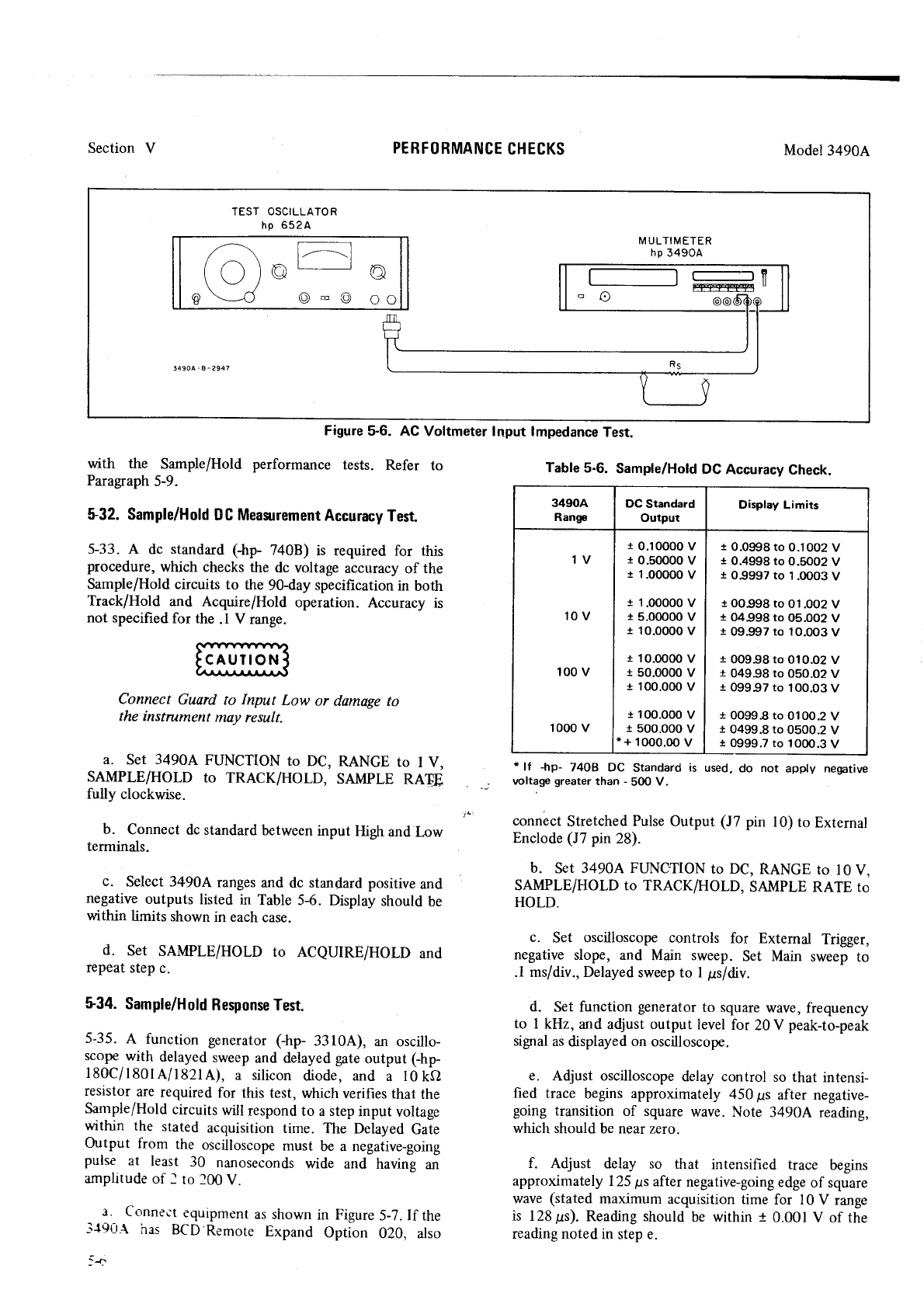
TEST OSCILLATOR
hp 652A
,,' \ l/-.----\l
(o)@L
'e
\- /
@'\--O @
- @ oo
M
ULTIMETER
hp
349OA
34904-A-?947
Figure
5-6. AC Voltmeter Input lmpedance
Test.
Section V PERFORMANCE
CHECKS Model
3490A
with the Sample/Hold performance tests. Refer to
Paragraph
5-9.
$32. Sample/Hold
BC Mea$rement
Aecuracy
Test.
5-33. A dc standard (-hp- 7a0B) is required for this
procedure, which checks
the dc voltage accuracy
of the
Sample/Hold circuits to the 90-day specification
in both
Track/Hold and Acquire/Hold operation. Accuracy is
not specified
for the .l V range.
Connect Guard to Input Low or damage to
the instrument mav result.
a. Set 3490A FUNCTION to DC, RANGE to I V,
SAMPLE/HOLD to TRACK/HOLD, SAMPLE RAT.A,
fully clockwise.
b. Connect
dc standard
between
input High
and
Low
terminals.
c. Select
3490A ranges
and dc standard positive
and
negative
outputs listed in Table
5-6. Display
should
be
within limits shown
in each
case.
d. Set SAMPLE/HOLD to ACQUIRE/HOLD and
repeat
step
c.
$34. Sample/Hold
Response Test.
5-35. A function generator (-hp- 3310A), an oscillo-
scope
with delayed
sweep
and delayed
gate
output (-hp
l80C/l80lAll82lA), a silicon
diode, and a l0kh
resistor
are
required
for this test,
which
verifies that the
Sample/Hold
circuits
will respond
to a step
input voltage
within the stated acquisition
time. The Delayed
Gate
Output from the oscilloscope
must be a negative-going
pulse at least 30 nanoseconds
wide and havins an
amphtude
of I to 100
V.
f,. Conne''r
equipment
as
shown
in Figure
5-7. If the
-r490A ha: BCD Remote Expand Option 020, also
i+
* lf -hp- 74OB DC Standard is used, do not apply negative
\roltage greater than - 5OO
V.
connäct
Stretched
Pulse
Output (J7 pin l0) to External
Enclode
(J7
pin 28).
b. SEt
3490A FUNCTION tO DC, RANGE tO IO V,
SAMPLE/HOLD to TRACK/HOLD, SAMPLE RATE to
HOLD.
c. Set oscilloscope
controls for External Trigger,
negative
slope, and Main sweep.
Set Main sweep
to
.1
ms/div., Delayed
sweep to I ps/div.
d. Set function generator
to square
wave, frequency
to I kHz, and adjust
output level
for 20 V peak-to-peak
signal
as
displayed
on oscilloscope.
e. Adjust oscilloscope
delay control so that intensi-
fied trace begins
approximately
450
ps after negative-
going transition of square
wave. Note 34904 reading,
which
should be near
zero.
f. Adjust delay so that intensified trace begins
approximately 125
ps
after
negative-going
edge
of square
wave
(stated
maximum
acquisition
time for l0 V range
is 128
ps). Reading should
be within 1 0.001
V of the
reading noted
in step e.
Table
5-6. Sample/Hold
DC
Accuracy
Check.
3490A
Range DC Standard
Output Display Limits
1V
10v
100 v
1000 v
r 0.10000 V
r 0.50000 v
r 1.00OO0
V
1 1.00000
v
r 5.00000 v
I 10.0000
V
r l0.0O0O
V
r 50.0000 v
r 100.000
v
1100.000
v
t 500.000
v
'+ 1000.oo
v
r 0.0998 to 0.1002
V
! 0.4998 to 0.5002 V
t 03997 to 1.0OO3
V
100998 to
01
.002 V
+ 04998 to 05.002
V
! 09.997 to 10.OO3
V
t 009.98 to 010.02 V
t 049.98
ro 05O.O2
V
I 099.97 to 100.03
V
t 0099"8 to 0100.2
V
! 0499.8 to 0500.2
V
r 0999.7 to 1OO0.3
V
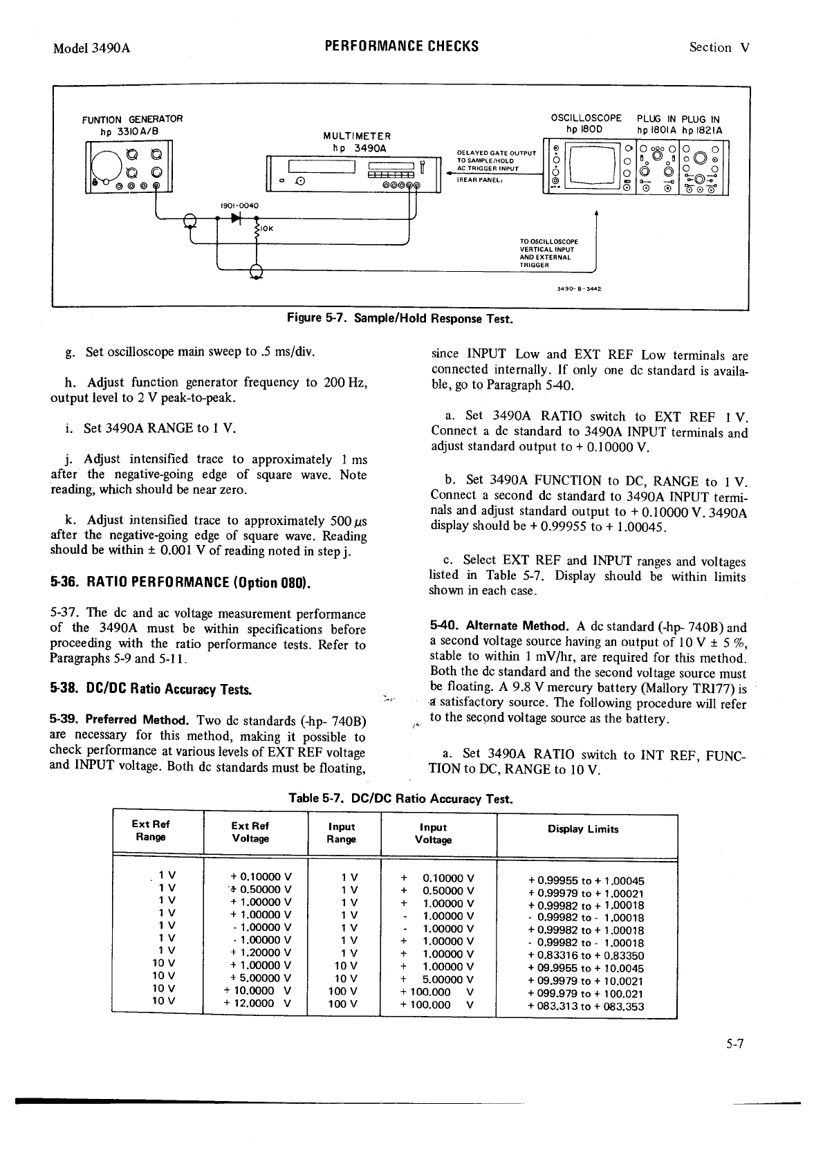
Model3490A
g. Set
oscilloscope
main sweep to .5 ms/div.
h. Adjust function generator
frequency to 200H2,
output level to 2 V peak-to-peak.
i. Set
349OARANGE
to I V.
j. Adjust intensified trace to approximately I ms
after the negative-going
edge of square wave. Note
reading, which should
be near zero.
k. Adjust intensified trace to approximately 500
ps
after the negative-going
edge of square
wave. Reading
should
be within t 0.001 V of reading noted
in step
j.
536.
RATI0
PEBF0BMANCE
(0ption
080).
5-37. The dc and ac voltage
measurement performance
of the 3490A must be within specifications before
proceeding with the ratio performance tests. Refer to
Paragraphs
5-9
and 5-l l.
$38. DC/DC
Ratio
Accuracy
Tests.
5-39. Preferred Method. Two dc standards
(-hp- 7a0B)
are necessary
for this method, making it possible to
check performance at various
levels
of EXT REF voltage
and INPUT voltage. Both dc standards
must be floating,
since IMUT Low and EXT REF Low terminals are
connected
internally. If only one dc standard
is availa-
ble,
go
to Paragraph
540.
a. Set 3490A RATIO switch to EXT REF I V.
Connect
a dc standard
to 3490A INPUT terminals
and
adjust
standard
output to + 0.10000 V.
b. Set 349OA
FUNCTION to DC, RANGE to 1
V.
Connect
a second
dc standard
to 3490A IMUT termi_
nals
and
adjust standard
output to + g.lgggg V. 3490A
display should
be
+ 0.99955 to + 1.00045.
c. Select
EXT REF and INPUT ranges
and
voltages
listed in Table 5-7. Display should be within limits
shovm
in each case.
540. Alternate
Method. A dc standard (-hp-
74OB)
and
a second
voltage
source
having
an output of l0 V + 5 %,
stable to within I mV/hr, are required for this method.
Both the dc standard
and the second
voltage
source
must
be floating.
A 9.8 V mercury
battery
(Mallory
TN77) is
.e
satisfaQtory
source.
The following procedure
will refer
" to the secgnd
voltage
source
as the
battery.
a. Set 34904 RATIO switch to INT REF. FUNC_
TION to DC,
RANGE
to 10
V.
PERFOHMANCE
CHECKS Section V
FUNTION
GENERATOR
hp 3310A/B
OSCILLOSCOPE
hp lSOD PLI.JG
IN PLUG
IN
hp
l80lA hp
l82lA
OELAYED
GATE
OUTPUI
TO
SAMPLE/HOLD
AC
TRIGGER
INPUT
Figure
$7. Sample/Hold
Response
Test.
Table 5-7. DC/DC
Ratio Accuracy
Test.
Ext Ref
Range Ext Ref
Voltage Input
Range
Input
Voltage Display Limits
1V
1V
1V
1V
1V
1V
1V
10v
10v
10v
10v
+
0.10000 v
'+
0.50000
v
+
1.00000v
+ 1.00000
v
- 1.00000 v
- 1.00000 v
+ 1.20000
v
+ 1.00000 v
+ 5.00000
v
+ 10.0000
v
+ 12.0000
v
1V
1V
1V
1V
1V
1V
1V
10v
10v
100
v
100
v
+ 0.10000
v
+ 0.50000
v
+ 1.00000 v
- 1.00000 v
- 1.00000 v
+ 1.00000
v
+ 1.00000
v
+ 1.00000
v
+ 5.00000 v
+
100.000 v
+
100.000 v
+ 0.99955
to + 1.00045
+
0.99979
to + 1.00021
+ 0.99982
to + 1
.00018
- 0.99982to-
1.00018
+
0.99982
to + 1.00otg
- 0.999821o-
1.00018
+
0.83316
to
+
0.83350
+ 09.9955
to + 10.0045
+
09.9979
to + 10.0021
+
099.979
to + 100.021
+ 083.31
3 to +
083.353
5-7
Section V
b. Connect the battery to IMUT terminals,
* to
HIGH, - to LOW.
Note
and
record
3490A display.
c. Connect dc standard to EXT REF terminals and
set standard output to positive voltage equal to display
noted
in step b.
d. SET 490A RATIO switch to EXT REF l0 V.
Display should be
+ 09.9982
to + 10.0018.
e. Reverse
polarity of dc standard output. Display
should be
-09.9982
to - 10.0018.
f. Set RATIO switch to INT REF. Reverse
polarity
ofbattery connections.
Note and record
display.
C. Set RATIO switch to EXT REF 10V. Adjust dc
standard output to negative voltage equal to display
noted in step f. Dsplay should now be +O9.9982 to
+ 10.0018.
h. Reverse
polarity of dc standard output. Display
should be -O9.9982
to - 10.0018.
i. Reduce dc standard output to 1/10 the output
used in step h.
j. Set RATIO switch to EXT REF lV. Display
should
be
-09.9982
to - 10.0018.
S41.
AC/DC
Ratio Accuracy Test.
5-42. A dc standard (hp- 7a0B) and an ac calibrator
(hp-7a5A) are required for this test. r...
a. Set 3490A RATIO switch to EXT REF I V.
Connect dc standard
to EXT REF terminals and adiust
standard
output to + 0.10000 V.
b. Set 3490A FUNCTION to AC, RANGE to I V.
Connect ac calibrator to IMUT terminals and adjust
calibrator output to l00mV at l00Hz. Display should
be
0.99865 to I
.00135.
c. Select EXT REF and INPUT ranges and voltages
listed in Table 5-8. Display should be as indicated in
each case.
Model
34904
5-43.
External Reference
Input Resistance
Test.
544. L dc standard
Chp-
7a0B)
and a l0k9"tO.l%
resistor
(-hp-
0698a157\ are
required
for this test.
a. Set 34904 RATIO switch to EXT REF l0 V.
FUNCTION
to DC, RANGE to l0 V.
b. Connect 3490A. dc standard and l0 k,f)
resistor as
shown in Figure 5-8. Connect
jumper across
resistor.
c. Adjust dc standard output to + 10.0000
V. Note
34904 display.
d. Remove
jumper across resistor.
Display should not
change more than 100 counts, verifying an EXT REF
input resistance
of ) l0? Q.
5-45.
GPIB 0PEBATIONAL
CHECK
(0ption
030).
546. A General
Purpose
Interface Bus system controller
and a printer are required to verify the operation of the
3490A Option 030. Two procedures are
given. The
first,
in Paragraph 547,is a
general procedure to be
used with
any bus controller. The second, in Paragraph 5-49, is
essentially the same procedure written specifically for
the 9820A calculator.
If the 3490A I/o circuits fail to
operate correctly, refer to the GPIB troubleshooting
information, P
ar agr aph
7 49 .
l. Initialize
LEOP - Set
End
Output [.ow
HEOP - Return End Output to iligh
LREN - Set
Remote Enable LOW
2. Send addresses
(see Paragraph 3-104 for 3490A
address codes)
LMRE Set
Multiple Response Enable LOW
? (77
s) - Universal unlisten command
6 (668) - 3490A listen address
(3490A placed
in re-
mote mode)
HMRE - Set Multiple Response Enable HIGH
programming
instructions
Test
No. I
PERFORMANCE CHECKS
3. Send
i)
rJ
Table 5-8. AC/DC Ratio
Accurary
Test'
Ext Ref
Range
Ext Ref
Voltage
I nput
Range
lnput
Voltage
Display Limits
iV
1V
1V
10v
10v
10v
10v
0.50000
v
1.00000
v
1.20000
v
1.00000
v
5.00000
v
10.ooo0 v
12.0000 v
1V
1V
1V
10v
10v
10v
10v
0.50000
v
1.00000
v
1.00000
v
1.00000
v
5.00000
v
10.0000
v
10.0000
v
0.99865
to 1 .00135
0.99865
to 1.00135
0.83218 to 0.8348
09.9865
to 10.0135
09.9865
to 10.0135
09.9865
to 10.0135
08.3218 to 08.3448
5€
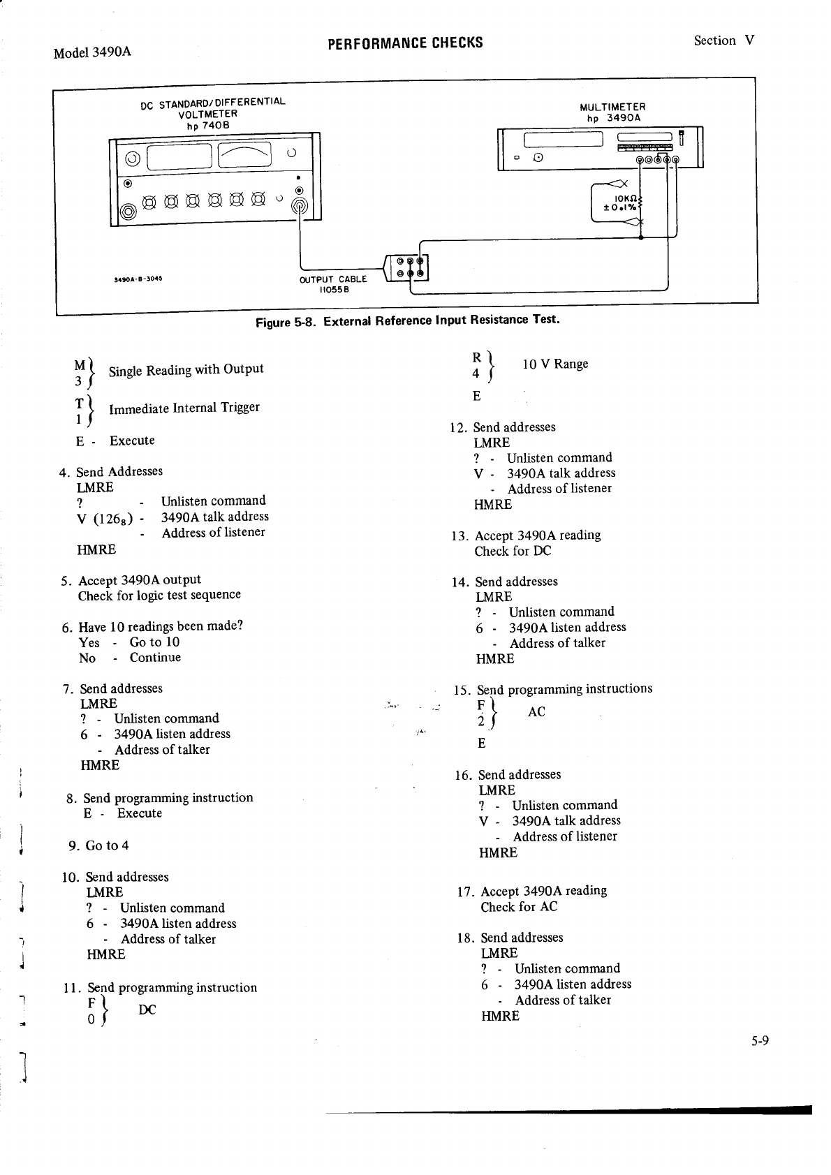
DC STANDARD/DIFFERENTIAL
VOLTMETER
ho
74OB
MULTIMETER
hp 349OA
34$A-l_5045 OIJTPUT
CABLE
il0558
PEBFORMANCE
CHECKS
Reference
Input Resistance
Test.
Section V
Model3490A
Figure
5-8. External
rr \
t: I Single
Reading
with OutPut
5)
I I Immediate
Internal
Trigger
r)
E - Execute
4. Send
Addresses
LMRE
2 - Unlisten
command
V (1268) - 34g}Atalkaddress
' Address
of listener
HMRE
5. Accept
3490AoutPut
Check
for logic test sequence
6. Have
10 readings
been
made?
Yes - Go
to 10
No - Continue
7. Send
addresses
LMRE
? Unlisten command
6 - 3490A
listen address
- Address
of talker
HMRE
8. Send
programming
instruction
E - Execute
Goto4
Send
addresses
LMRE
? - Unlisten command
6 34904 listen
address
- Address of talker
HMRE
12. Send
addresses
l-l\,tRE
? Unlisten
command
V - 3490A
talk address
- Address
of listener
HMRE
13. Accept
3490A
reading
Check
for DC
14. Send
addresses
LMRE
? Unlisten command
6 3490Alisten address
- Address
of talker
HMRE
15. Send
programming
instructions
. El
. :} AC
zt
E
16. Send
addresses
LMRE
'! Unlisten command
V - 3490A
talk address
- Address
of listener
HMRE
17. Accept
3490A
reading
Check
for AC
18. Send
addresses
LMRE
'l Unlisten comrnand
6 - 3490A
listen
address
- Address
of talker
HMRE
R
4
E) lo v Ranse
9.
10.
I
l
't I l. Send
programming
instruction
trl
öt DC
5-9
Section V
19. Send
programming
instructions
il Ko
tl
pl
: I .l kQ Range
ol
E
20. Send addresses
LMRE
? Unlisten command
V - 3490A talk address
- Address
of listener
HMRE
21. Accept
349}Areading
Check for KO and .l kSl range
22. Send
addresses
LMRE
't Unlisten
command
6 - 3490A
listen
address
- Address of talker
HMRE
23. Send
programming
instructions
:t lkQRange
),
E
24. Send addresses
LMRE
? Unlisten
command
V - 349OA
talk address
- Address
of listener
HMRE
25. Accept
3490A reading
Check for I kO range
26. Send
addresses
LMRE
2 Unlisten
command
6 3490A
listen
address
- Address
of talker
HMRE
27. Send
programming
instructions
RI
a I l0 kf,) range
al
E
lE. Send
addresses
L\{RE
? Unlisten
command
V - 3490A
talk address
- Address
of listener
HMRE
r-10
PERFORMANCE
CHECKS
29. Accept
3490A reading
Check
for l0 kO range
30. Send
addresses
LMRE
? - Unlisten
command
6 - 3490A
listen
address
- Address
of talker
HMRE
3l . Send
programming
instructions
RI
;' ) 100 kO Range
rt
E
32. Send
addresses
LMRE
? - Unlisten
command
V - 3490|talk address
- Address
of listener
HMRE
33. Accept
3490
Lreading
Check for 100
kQ range
34. Send
addresses
LMRE
? - Unlisten
command
6 - 3491Alisten
address
- Address
of talker
HMRE
35. Send
programming
instruction
,PI
; l 1000 kO
range
z)
E
36. Send addresses
I.IURE
'! Unlisten
command
V - 3490A talk address
- Address
of listener
HMRE
37. Accept
34g}Areading
Check for 1000
kQ range
38. Send
addresses
LMRE
? - Unlisten command
6 3490A listen
address
- Address
of talker
HMRE
39. Send
programming
instructions
RI
;' ) 10,000
kQ range
t)
E
Model
3490A
Model 3490A
Send
addresses
LMRE
2 - Unlisten
command
V - 3490A
talk address
- Address
of listener
HMRE
Accept
349D[reading
Check
for 10,000
kQ range
Send
addresses
LMRE
2 - Unlisten
command
6 - 3490[listen
address
- Address
of talker
HMRE
43. Send
programming instructions
IT
:' Interrupt single with output
E
44. Check
for SRQ LOW after 3490[completes a reading
45. Send
address and command
LMRE
V 3490A talk address
- Address of listener
(30a) - Status
Poll Enable command
HMRE
46. Accept
ASCII character from 3490A
Check
if LDIOT is LOW
47. Send addresses
LMRE
? Unlisten command
6 3490A
listen
address
- Address
of talker
HMRE ,."
48. Send
programming
instructions
M)
t I Single reading
with outPut
E
49. Send address
and
command
I-I\,IRE
V3490A
talk
address
Address
of listener
Status
Poll
Enable
command
50. Accept ASCII character
from 34gOA
Check if LDIOT is HIGH
5l . Send address
and
command
- Universal
untalk address
(31e) - Status
Poll
Disable
command
Section
V
52. Return
to local
HREN
$47. General Test Procedure.
548. This procedure
checks the ability of the 34904
GPIB circuits to accept and process
addressing
and
remote
programming,
and to output measurement
data.
This procedure
may be used with any bus system
controller.
$49. Test Procedure
Using
Model
98204 Calculator.
5-50. this test sequence
is written specihcally
for the
-hp Model 9820A Calculator,
and
performs
the same
operating
checks
as
the general procedure
in Paragraph
547. Tllre
9820A must
have the I I l44A Interface
and
the Peripheral
Control
II ROM
Block
installed.
Refer
to
the Operating
Manuals for these instruments for opera-
ting instructions.
The following
test sequence may be
recorded on an
-hp Calculator
Program Card
and
used in
subsequent tests
and
in troubleshooting. The
program
is
presented
in this procedure
in the form that it is
printed
by the 9820A.
The first statement
gives
an
example
of
the
9820A keyboard
sequence
required.
Initialize
the
calculator
and 3490A by prpssing
EXECUTE
(End Output, EOP, is LOW while STOP
key is de-
pressed)
Set
LREN
to LOW.
f-r r
ri.{"t' '','r! llf.rT' {'-rl
T t't | | .J I d_ ! r.r.rr:.
I I.:'r
The
above
sequence
requires
that the following
keys
be
pressed
PERFOHMANCE
CHECKS
40.
41.
42.
(30a)
HMRE @o@o@o
STORE
r-T\
EUJ[I
Set
counter
to l.
1r
Ir
1
+
tll-
5-l I
Section
VPERFORMANCE
CHECKS Model 3490A
Address
3490A to listen, calculator
to talk. 9820A talk Address
3490A to listen, 9820A to talk. Program
Ohms
address
is u. This puts 34904 in remote control.
Program function, .l ke range.
3490A to Test No. l, Single Reading with Output,
Immediate Internal Trigger. j. rjj
I
t"':
i'i i't " ''':'r:l'
l"'i
" I " i:::'
I i.;:
*' i::i'
:r , { .i,ü.i
t:::
i',i i::l ' ',:'r:i
i".l
" r " i::
i;i
[i:'
::';'1 ] i "1
'-'
r-'
::::ll"1[::"
l"- Address
3490A'to talk, 9820A to listen. Accept
3490A
Address
calculator to listen, 34go^ to talk. calculator reading
check for Ko function'
listen address
is 5.
Accept
34904 reading. :i.
:1.
I
::::!
I i:::l'll:l " 'lr"'rr;
" i Fi:l.'t[:il i:.iil
r::::f,.li:r
"
i:j ,.," H"'
ii F: i,l'.l"
:+
ir ; i I..i,:,i1,'T',,
,
;i:i;;
l;,i
l;.::i:i[
F;: ä il l.
::i
r f:l i". fj F:
l- ,,
l:.
r.-i
,,
i_.
Instruct calculator to print reading, trigger
3490A,
print the
next reading,
etc., until a total of l0 readings have
been Instruct 9820A to check
last character of output format
taken
and
printed,
then
go
to 6. (see
Paragraph34T).
Check
for .l kSl range.
4r :i;il
p':,:i
l"i i:i I i:i;;'
-[' t:::t
i 'l F [t Fi: i.t fiil i.
:.i:l
"i',ii:i
ii i. l-:' t"..:;.
i. llt
* 1 üj
i ._t
f,l |;i i: l" ii i ,r
!::: -ur-.:
ii
...,1
l''l
F llr i*
flir i':l:
._t n
:i
+.[rt-,'ht
i t::::l''l]:t
"',lri,i-l " r i F .1
- '::!lii;::::1:-, ] ['f:'"i'
" [ " ii
,_ti1pt
-*:l- i i,:.
" i"-
Address
3490A to listen,
9820A to talk. Program
3490A to
Address
34gOA to listen,
9820A to talk. Program
3490A to I kO range.
DC function, l0 V range. I q I
t, : i:":i'lll " 'i i:,
l,-l
" r " |:i:
l::;
i::
" i-
i-.i.{ ii 'r '-' j. | | r! rr r i-J t..i ji t-.
r-, l l L.r : l::1 l-l I l- I;;.t
1',:.
,.1 t.
"F.
r... Address 3490A
to talk,9820A
to listen.
Address
3490A
to talk, g82OA
to listen.
Accept
34g0A .i
I I
reading.
Check for DC function. l"::i'l
Il :
d:' i','i
f; " ii 1.
{'i-:
i-'
i!
r:::i''ii:r
'
'::'
""
:::'
"
i ü:l-rii::r :i
:.li ä'"1'JJ':li3'^,rl, lg;,lt'i::r;Y?ä
,:""r;l"k
rast
+
,:l ii [:i: .i.i[il ].
:jt i';,,::
i [;::it
hi
:i.
:;il
-:'',:::
ii I t- ii'::::1;,;r1
i :i
i:i, !
li [: -1" " it t-:
' F. i',, I,[' 1.
:;;t
"i,.,1'
l; 1
p: r".:
::;.
i. :.i:t
I i +.r,::-i
i.-:
li ..1 l{ Fi lil i-
i.ir
Address
3490A
to listen,98204
to talk. Progam
34904
to i F. ..:1.....
dl
i:li::::
l; i i;::,i;:,.i..
,,
:i.
AC function. r.i
,,
i
!:, '
i: i'iii ' '1ij i i " , " [:: .;i::[:
" l'" Address 349olto listen,9g20A
to talk.
prosram
34904
to
l0 kO range.
Address
3490A to talk, 9820A to listen. Accept 3490A i l:il I
reading.
Check
for AC function. r.":
ii j..r " 1'1,
!.-i
" r " Iii:
,,:i
il::
" i."
i_ i: Ii ' ':.",,,,
i ' ; il;:.1)
[::t ].
::;rl
* f i E:IrE: l,
,;r-:*;'
I i:;,::1.:r[:ir Address 3490A
to talk,
9820A
to listen.
_.;+l;ip ll::::i,ii
i li;r I
;;:'itr- f t::f,ll.l
.t:iri,,rilx"I:l,,,r:-:i-.
5-l l
Model
3490A
Accept 3490A reading. Instruct 98204 to check last
character
of output format.
Check
for l0 kSl range.
,: r:t tr
Fi IlLt :l ::l
't il i I [:r t-.::i;
:l ;ll
i 1
+'t-:..+
t-:
I .-l
l'l
F lir
1""
I F "i'..".;{
ili
:::
4.
[ l:r,ü,"1"
" ].
Hfi " l-.
Address
3490A
to listen,9820A
to talk.
Program 3490A to
100
kO range.
d:.: r
L:t,lIt "''i:'rl,Ll
" r " [i:::xtH
" l"
Address
3490A
to talk,982OA
to listen.
t::f'l
It " {' r,,,r
l; " li I "!
t::
l-
Accept 3490A reading.
Instruct 9820A
to check
last
character
of output
format.
Check
for 100
kO range.
cLt:
l':. .Ll Ei I ..:'
":'L t I I- r.- :i I ..:'
! { r r-. r r-.r lrJFr i-rl
! I -r t-. ":r't_.
! .-t
l'l r [.t T"
,:: .-l !
TT
L T r. _- !+,:t _..::, ! r F. I I
l:-l l:l fr. f'
Address
34904 to listen,9820A
to talk. Program
3490A to
1000
kO
range.
C.|:t !
r-,
l llr :' |:' r-r I l.:. c. I: T
Address
3490A to talk,9820A
to listen.
r-.
I't Ir :' ,,,
,-r ! I "r r.-.
r'
Accept 3490A reading. Instruct 9820A to check last
character
of output format.
Check
for I
000
kQ range.
L: r:' r
["i IlEl I :il
.+
I I 1 ;: r::::i
I ::i
i 1
r"r*:+t::
i ,.-tf,1F
rjtl".
IF r*'4r:r*!it'F:T
"I
ütJtJl'::"F
Address
3490A
to listen,
9820A to talk. Program
34904
to
IO,OOO
kQ range.
t::i'1It " ';'t,
l-i
" I ,'
t: i h"
,,
i"
Address
3490A
to
talk,9820A
to listen.
.j' l. .
r:
f,l Ir "
';'i"5
" i 1
.+
r::
i.-
Section
V
Accept 3490A reading.
Instruct 98204 to check last
character
of output
format. Check
for 10,000 kO range.
i':Ilhl :i,
:;i'+
;:t
li 1'
F l"::
:;: I ::::l
I l.
+.r".:1! t:':
ii
.."t
|',] l-,, i:l t"
.i: f ijl
.".,i
tjil::r
I i i:r fi:
"1' ,' :i,
g I'
tj;tti:ilili':'"
l'"
Address 3490A
to listen,
9820A
to talk. Program
3490A
operating mode
to Interrupt
Single
with
Output.
.._,
.t ,
i-:
t,l l.t " dl
rl,
l...l
" r " [,i;'H " l-'
Check Service
Request line. If line is LOW,
go
to 36.
..1' .*l r
[: It:::; I :;l
":,1:1
I .-l
1,1 t"' |::i:,. .|.
td
Address 3490A to talk, 9820A to listen.
Send Status Poll
Enable.
Check 3490A response to SPE
on data line LDI07.
r*,
l llr r,,
....r ..- rlll :r rr. Ir tj .i-
..lrTtr,:r
IT U'.,rE..:1 rrF.I
" L it '[ t];:' I ::; ['"
t-t lil " F
Address 3490A to listen, 9820A to talk. Program
3490A
operating
mode to Single
Reading
with Output.
.-ri r
ia F.l.l1 !r r-i r- | | r r' t..{,.-r f- I I
r.-.
l'l Ir :' (:, t-t ! l'|..:' r I."
Address
3490A to talk, 9820A to listen.
Send
Status
Poll
E_nable.
Check 3490A response
to SPE on data line LDIO7.
ia.:
i1 tJT' r'itH:rr,..'!rrr.'fir'i .i
l_..
l l Il r,r ..-l i- ':' I r:. .L.l I:' .:.
.: -r !_.. t! .i. r- r-., L |:' ,:' ! t- F. I
"Lfi
i,;';'' I:l; HIr;1-1,,p
Send universal
untalk address
and Status Poll Disable
command.
j-. t.{ l,i il ,. $r f1 r I
Set LREN
line to HIGH and
end
program.
,t {.1 n
i" T.{ -t" r..r .i .'.:r r I i t..i -r. { ri I
r t.t I i .i. :r ,::.. ! l.t.t
t.r. | .j.
.: r-
ri.i r
F: hi tl t,.,.
PERFORMANCE
CHECKS
5-l
3
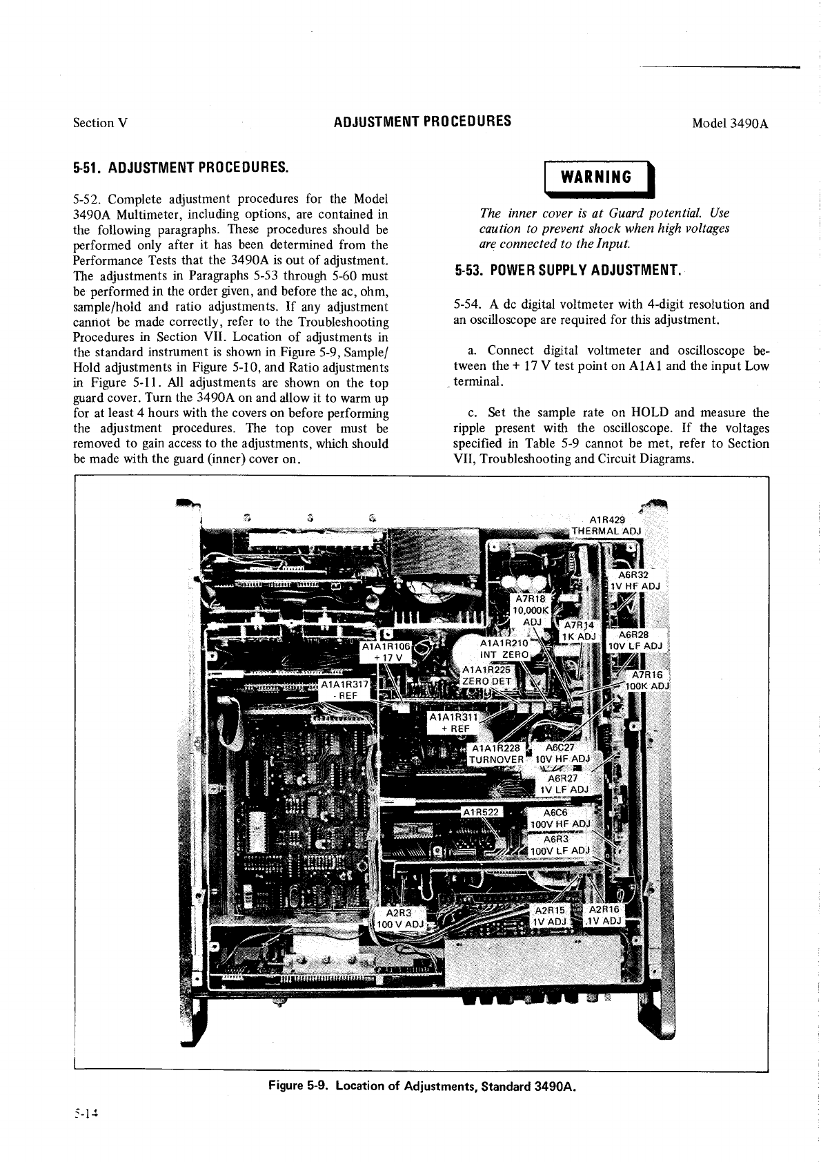
Section
V
$51.
ADJUSTMENT PROCEOURES.
5-52. Complete adjustment
procedures
for the Model
3490A Multimeter, including options, are contained in
the following paragraphs.
These
procedures
should be
performed only after it has been determined from the
Performance Tests
that the 3490A is out of adjustment.
The adjustments
in Paragaphs 5-53 through 5-60 must
be performed in the order given,
and before the ac, ohm,
sample/hold
and ratio adjustments. If any adjustment
cannot be made
correctly, refer to the Troubleshooting
Procedures
in Section
VII. Location of adjustments in
the standard
instrument
is shown
in Figure
5-9, Sample/
Hold adjustments
in Figure 5-10,
and Ratio
adjustments
in Figure 5-l l. All adjustments are shown on the top
guard
cover.
Turn the 3490A
on and
allow it to warm up
for at least 4 hours with the covers on before performing
the adjustment procedures.
The top cover must be
removed
to gain
access
to the
adjustments,
which should
be
made with the guard (inner)
cover
on.
ADJUSTMENT
PROCEDURES Model
3490A
wARiltr{G
The inner cover is qt Guard potential. Use
caution to prevent shock when high voltages
are connected
to the
Input.
5.53.
POWEB
SUPPLY
ADJUSTMENT.
5-54. A dc digital voltmeter with 4digit resolution
and
an oscilloscope are
required
for this adjustment.
a. Connect digital voltmeter and oscilloscope
be-
tween the
+ 17
V test
point on AlAl and the input Low
terminal.
c. Set the sample rate on HOLD and measure
the
ripple present with the oscilloscope.
If the voltages
specified in Table 5-9 cannot be met, refer to Section
VII, Troubleshooting
and
Circuit
Diagrams.
f,:
Al F429
THERMALADJ.
w
46R28 i
lOV
LF
ADJ
J
fi=i"l;
A7R16
i
1OOK ADJ
Figure
5-9. Location
of Adjustments,
Standard
3490A.
i !!
Model3490A
d. Check
other power supply
voltages by connecting
digital
voltmeter and oscilloscope
to test
points
listed in
Table
5-9. If any voltage
is not correct,
refer to Section
vu.
Table
5-9. Power SUPPIY
Voltages.
A1A1
Test
Point Voltage Ripple*
+ 17\l
+ 5V
+30V
- 17V
- 5V
-
30v
+
16.99
to
+
17.01 V
+ 4.995 to + 5.075 V
+ 30.10 to + 30.90
V
- 16.9 to
- 17.1 V
- 5.00 to - 5.85 V
- 30.10 to- 30.90V
< 50
mV p-p
< 60
mV p-p
( 25
mV p-p
< 50 mV p-p
(60mVpp
(25mVp{
*All ripple measurements are with the Sample
Rate
on
HOLD.
5.55.
DC
ZERO ADJUSTMENTS.
5-56. A dc standard
(-hp- 7a0B) and
a dc voltmeter able
to resolve
l0 pV are
required for these
adjustments.
a. Connect
dc voltmeter
between
AlAl test
point A
and
input Low terminal.
b. S€t 3490A SAMPLE RATE control fully counter-
clockwise to HOLD position.
c. Adjust AlAlR2l0 (lntZero) for voltmeter
read-
ing of 0 r 150 gV. Disconnect
voltmeter.
d. Set FUNCTION to DC. RANGE to l0 V. SAM-
PLE RATE to FAST.
e. Connect
dc standard
to 3490A input and adjust
standard
output to + 0.00100 V.
f. Adjust AlAlR225 (Zero DetecI kvel) for maxi-
mum reading
on 3490A display. Note reading.
C. Reverse
polarity of input and adjust AlAlR228
(Tumover) for reading noted in step f. Continue
reversing
input polarity and adjusting
AlAlR228 until
positive
and negative
readings
are equal.
h. Apply + 0.00100
V input to 3490A. Adjust
AlAlR225 (Zero Detect kvel) for 3490A display of
+ 00.0010.
$57. REFERENCE
ADJUSTMENTS.
5-58.
A dc standard
(hp-
7a0B)
is
required for these
adjustments.
Guqrd Terminal should
be
connected
to Low
or damage
to the instrument may result.
a. Set 3490A FUNCTION
to DC. RANGE to t0 V.
AOJUSTMENT
PROCEDURES Section
V
b. Connect
dc standard
to 3490A
input and
adjust
standard
output to
- 10.0000
v.
c. Adjust
AlAlR3ll (+Ref)
for 3490A
display
of
-
10.0000.
d. Set
3490A
FUNCTION
to TEST,
RANGE
to 3.
Adjust
AlA1R3l7 (-
REF)
so
that
positive
and negative
display
readings
are equal
within I count. Last digit
must
be
between
2 and
9
(0.9999x).
If not,
repeat
steps
a through
d. Dsconnect
dc
standard.
5.59. DC
AMPLIFIER
ADJUSTMENTS.
560. A dc standard
(hp- 7a0B) is required
for these
adjustments.
a. Set
349OA
FUNCTION
to DC, RANGE
to .l V.
Short input terminals
with a copper
bar or heavy
solid
copper
wire.
b. Adjust
AlR429, accessible
through
hole in rear
panel,
for 3490A display
of 0 r .000002.
c. Set
3490A
RANGE to I V.
d. Remove
short from input terminals
and
connect
dc standard. Adjust
standard
output
to
- 1.000000
V.
e. Adjust
A2Rl5 (l V Adj) for 3490A
display
of
- 1.00000.
f. Set 3490A RANGE to 100
V, and adjust
dc
standard
output to
- 100.000
V.
g. Adjust
A2R3
(100
V Adj) for 3490A
display
of
- 100.000.
Reduce
dc standard
output
and disconnect.
h. Set
3490A
FUNCTION
to TEST,
RANGE
to 6.
Short input terminals
and note
amount
and
polarity of
oTfset
reading.
i. Remove short
and
apply
- 10.0000
V input.
Adjust
A2Rl6 (0.1
V Adj) for display of - 1000.00,
minus
(algebraically
subtracting)
the
offset noted in step
h.
$6I. AC
CONVERTER
ADJUSTMENTS.
5-62. Adjustment
of the dc circuits, Paragraphs
5-53
through
5-60, must
be completed
before
beginning
this
procedure.
An ac calibrator
(-hp- 745A) with a correc-
tion factor chart is required
for these
adjustments.
Guard
covers must
be in place
for this
procedure.
5-63. I V Range Adjustments.
a. Set
3490A
FTINCTION
to AC. RANGE to I V.
b. Connect
ac calibrator
to 3490A input.
Set
calibra-
tor output to I .000000 V at 100
kHz
(using
correction
factor
chart
as necessary).
s-l 5
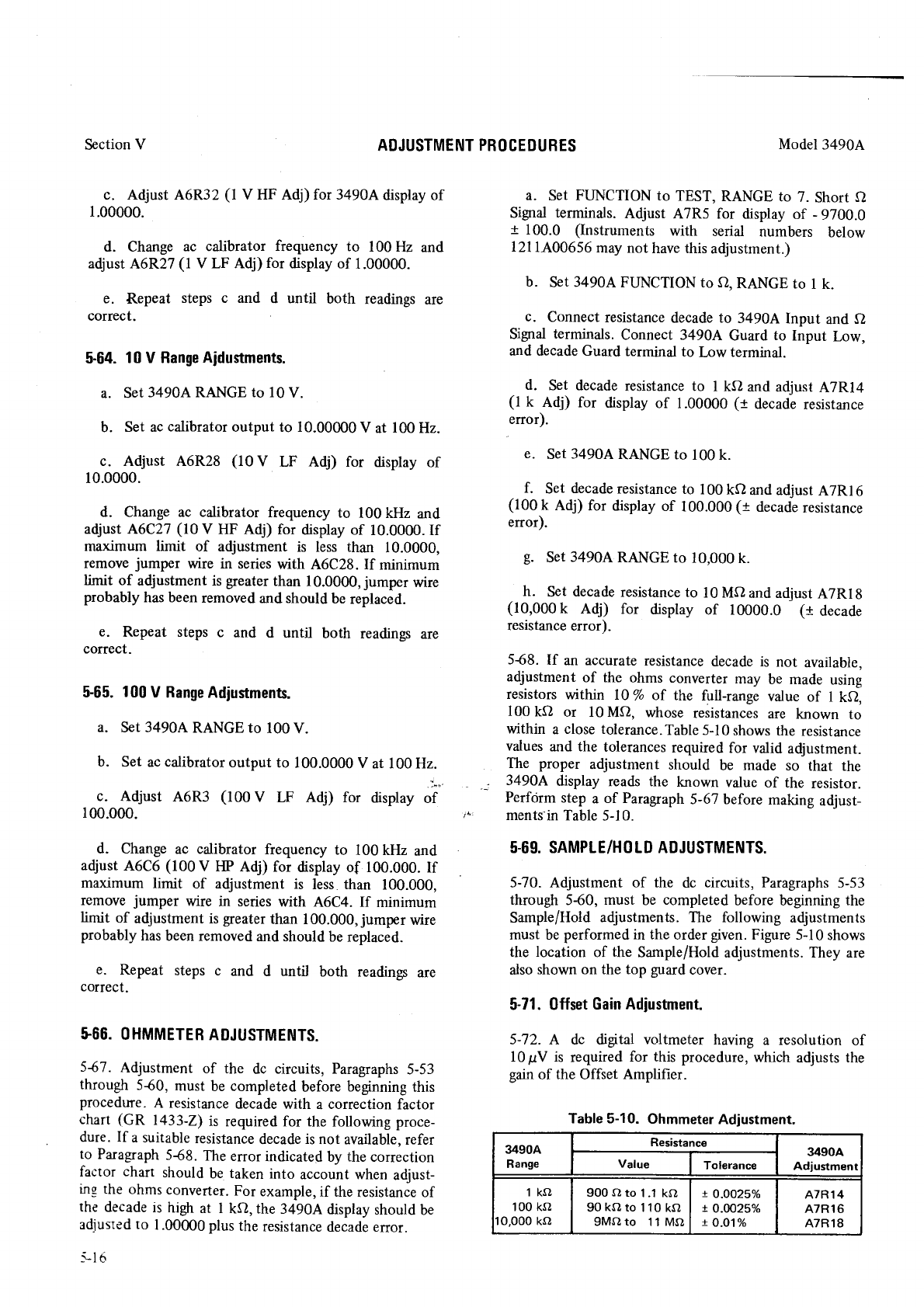
Section
VADJUSTMENT
PROCEDUBES Model
34904
a. Set FUNCTION to TEST, RANGE to 7. Short Q
Sigral terminals. Adjust A7R5 for display of - 9700.0
t 100.0 (Instruments with serial numbers below
l2l1A00656 may not have this
adjustment.)
b. Set
3490A
FUNCTION to O, RANGE to I k.
c. Connect
resistance
decade to 3490A Input and
O
Signal terminals. Connect 3490A Guard to Input Low,
and decade Guard terminal to Low terminal.
d. Set decade
resistance to I kfl and adjust
A7Rl4
(l k Adj) for display
of 1.00000
(r decade
resisrance
error).
e. Set
349OA
RANGE to 100 k.
f. Set decade
resistance
to 100
kQ and adiust
A7Rl6
(100
k Adj) for display
of 100.000
(t decade
resistance
error).
C. Set
3490A RANGE
to 10,000
k.
h. Set
decade
resistance
to 10 M{-2
and adiust
A7Rl8
(10,000
k Adj) for display of 10000.0 (t decade
resistance
error).
568. If an accurate
resistance
decade is not available,
adjustment
of the ohms converter
may be made using
resistors within l0 % of Ihe full-range value of I ke,
100
kf,} or l0 MO, whose resistances
are known to
within a close tolerance"Table
5-10
shows
the resistance
values
and the tolerances
required
for valid adjustment.
The proper adjustment should be made so that the
3490A display reads the known value
of the resistor.
Perfcirm
step a of Paragraph
5-67 before making a_djust-
ments
in Table
5-10.
5.69. SAMPLE/HO LD ADJUSTMENTS.
5-70. Adjustment of the dc circuits, Paragraphs
5-53
through 560, must be completed
before beginning
the
Sample/Hold
adjustments. The following adjustments
must be
performed in the order
given.
Figure 5-10
shows
the location of the Sample/Hold adjustments. They are
also
shown on the top guard
cover.
5-71. 0ffset
Gain Adjustment.
5-72. A dc digital voltmeter having a resolution of
l0pV is required
for this procedure,
which adjusts the
gain
of the Offset Amplifier.
c. Adjust A6R32 (l V HF Adj) for 3490A
display of
1.00000.
d. Change ac calibrator frequency to 100 Hz and
adjust
A6R27 (1 V LF Adj) for display of 1.00000.
e. Repeat steps c and d until both readings are
correct.
5-64.
10 V Range
Ajdustments.
a. Set
34904 RANGE to 10
V.
b. Set ac
calibrator
output to 10.00000
V at 100 Hz.
c. Adjust A6R28 (10 V LF Adj) for display of
10.0000.
d. Change ac calibrator frequency to 100 kHz and
adjust A6C27 (10 V HF Adj) for display of 10.0000. If
maximum limit of adjustment is less than 10.0000,
remove jumper wire in series
with A6C28.If minimum
limit of adjustment is greater
than 10.0000,
jumper wire
probably has been
removed
and should
be replaced.
e. Repeat steps c and d until both readings are
correct.
5-65.
100
V Range Adjustments.
a. Set 3490A
RANGE to 100
V.
b. Set ac calibrator
output to 100.0000
V at 100 Hz.
,o;.o$|j"rt A6R3 (100
V LF Adj) for display of tL
d. Change ac calibrator frequency to 100 kHz and
adjust
A6C6 (100
V HP Adj) for display of 100.000.
If
maximum limit of adjustment is less than 100.000,
remove jumper wire in series
with A6C4. If minimum
limit of adjustment is
greater
than 100.000,
jumper
wire
probably
has
been removed
and should
be
replaced.
e. Repeat steps c and d until both readings are
correct.
$66.
O
HMMETER
ADJUSTMENTS.
567. Adjustment of the dc circuits, Paragraphs
5-53
through 5{0, must be completed
before
beginning
this
procedure.
A resistance
decade with a correction
factor
chart (GR 1433-Z)
is required for the following proce-
dure.
If a suitable
resistance
decade
is
not available.
refer
to Paragraph
548. The
enor indicated
by the
correction
factor chart should
be taken
into account when
adiust-
ins the ohms
converter.
For example,
if the
resistanöe of
the decade
is high at I kQ, the 3490A
display
should
be
adiusted
to 1.00000
plus
the
resistance
decade enor.
_i-16
Table 5-10. Ohmmeter
Adjustment.
3490A
Range
Resistance 3490A
Adlustment
Value Tolerance
1ko
100 ko
0,000 ks,
900
o to
1.1 ko
90kato110ka
gMA
to 11 MO
L O.OO2'yo
t O.OO25o/o
! O.O1oÄ
A7R14
A7R16
A7R18
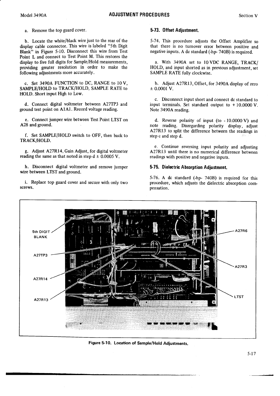
Model3490A
a. Remove
the toP guard cover.
b. Locate the white/black wire just to the rear
of the
display cable connector. This wire is labeled "5th Digit
Blank" in Figure 5-10. Disconnect this wire from Test
Point L and connect to Test Point M. This restores the
display
to five full digits for Sample/Hold
measurements,
providing greater resolution in order to make the
following adjustments
more accurately.
c. Set 3490A FTINCTION
to DC, RANGE to IO
V.
SAMPLE/HOLD to TRACK/HOLD, SAMPLE RATE to
HOLD. Short input Higfr
to Low.
d. Connect digital voltmeter between A27TP3 and
ground
test
point on AlAl. Record
voltage reading.
e. Connect
jumper
wire between
Test
Point LTST on
A28 and
ground.
f. Set SAMPLE/HOLD switch to OFF. then back to
TRACK/HOLD.
g. Adjust A27Rl4, Gain Adjust, for digital voltmeter
reading
the same as that noted in step
d I 0.0005 V.
h. Dsconnect digital voltmeter and remove
jumper
wire between
LTST and
ground.
i. Replace top guard cover and secure
with only two
screws.
ADJUSTMENT
PROCEDURES Section
V
5-73. 0ffset
Adjustment.
5-74. This procedure adjusts the Offset Amplifier so
that there is no turnover error between positive and
negative
inputs. A dc standard
(-hp 7a0B) is required.
a. With 3490A set to IOVDC RANGE, TRACK/
HOLD, and input shorted
as in previous
adjustment,
set
SAMPLE RATE fully clockwise.
b. Adjust
A27Rl3, Offset, for 3490A display
of zero
t 0.0001
v.
c. Dsconnect input short and connect dc standard
to
input terminals.
Set standard
output to + 10.0000
V.
Note 3490A
reading.
d. Reverse
polarity of input (to - 10.0000
V) and
note reading- Disregarding polarity display, adjust
A27Rl3 to split the difference between the readings in
step
c and step
d. I
i'
e. Continue reversing
input polarity and adjusting
A27Rl3 until there
is no numerical
difference
between
readings
with positive
and
negative
inputs.
$75. Dielectric
Absorption
Adjustment.
5:76.
A dc standard (hp- 7a0B) is required for this
procedure, which adjusts
the dielectric absorption com-
pensation.
sth
DtGtT
BLANK
A27TP3
A27R14
A27R13
Figure
5-10. Location
of Sample/Hold
Adlustments.
5-17
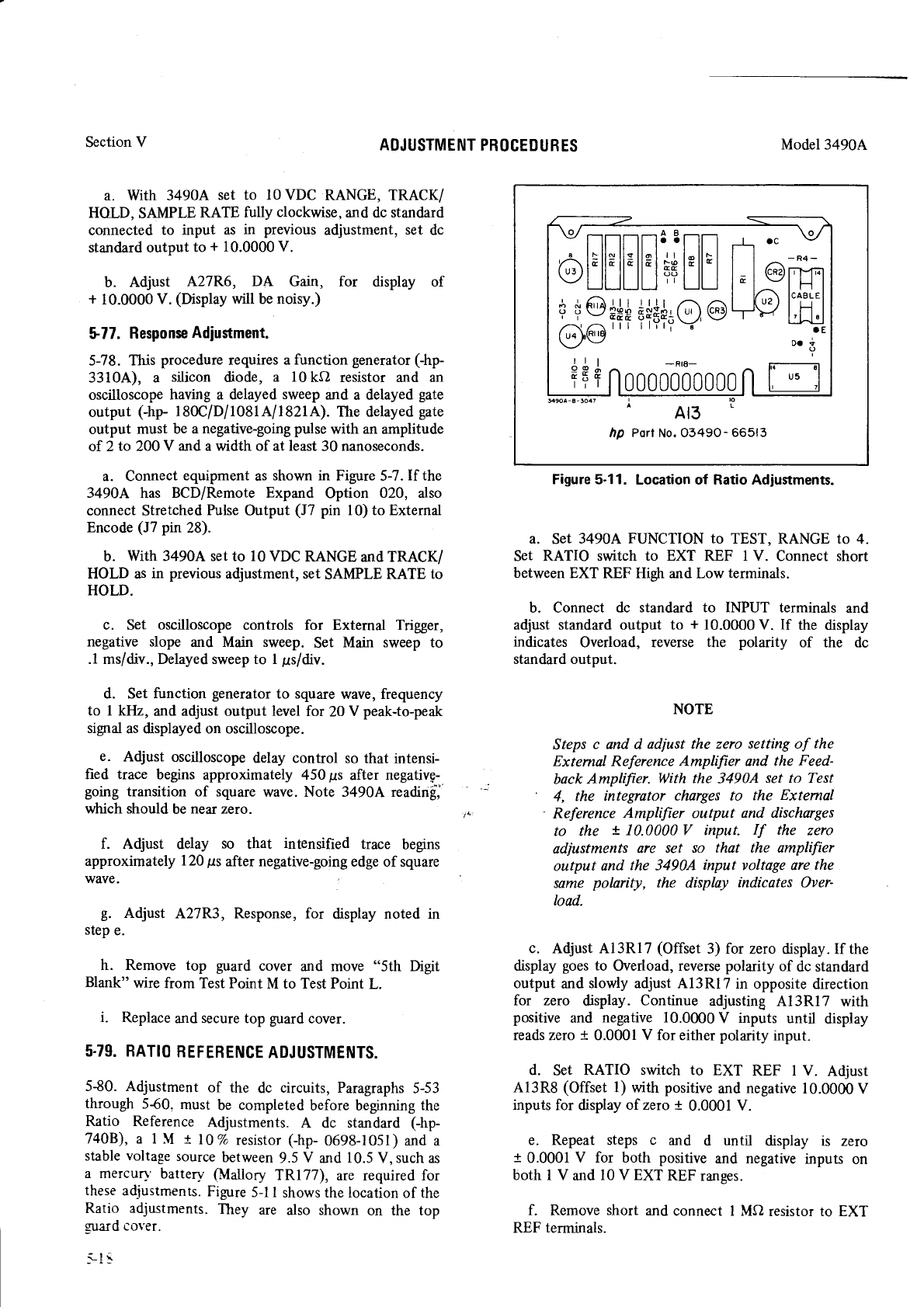
Section V AOJUSTMENT
PROCEDURES Model 3490A
a. Set 3490A FUNCTION to TEST, RANGE to 4.
Set RATIO switch to EXT REF lV. Connect short
between
EXT REF Hig[ and Low terminals.
b. Connect dc standard to INPUT terminals and
adjust standard output to + 10.0000 V. If the display
indicates Overload, reverse the polarity of the dc
standard output.
NOTE
Steps c and d adjust the zero setting of the
Extemal Reference Amplifier and the Feed-
back
Amplifier. llith the 34904 set to Test
' 4, the integrator charges to the Extemal
' Reference Amplifier output and dischmges
to the ! 10.0000 V input. If the zero
adjustments are set so that the amplifier
output and the 3490A input voltage are the
same polaity, the dßplay indicates Over-
load.
c. Adjust Al3Rl7 (Offset 3) for zero display. If the
display goes to Overload, reverse polarity of dc standard
output and
slowly adjust Al3Rl7 in opposite
direction
for zero display. Continue adjusting A13Rl7 with
positive and negative 10.0000
V inputs until display
reads zero
I 0.0001 V for either polarity input.
d. Set RATIO switch to EXT REF I V. Adjust
A13R8 (Offset 1) with positive
and
negative
10.0000V
inputs
for display
of zero t 0.0001
V.
e. Repeat steps c and d until display is zero
t 0.0001
V for both positive and negative
inputs on
both I V and
10 V EXT REF ranges.
f. Remove
short and
connect I Mf2
resistor to EXT
REF terminals.
a. With 3490A set to l0 VDC RANGE, TRACK/
HOLD, SAMPLE RATE fully clockwise,
and dc standard
connected to input as in previous adjustment, set dc
standard output to + 10.0000 V.
b. Adjust A27R6, DA Gain, for display of
+ 10.0000
V. (Display will be
noisy.)
S77. Response
Adjustment.
5-78. This procedure
requires
a function generator
(-hp-
3310A), a silicon drode, a l0kQ resistor and an
oscilloscope
having a delayed
sweep
and a delayed
gate
output (-hp l80C/DllOSlAllS2lA). The delayed
gate
output must be a negative-going pulse
with an amplitude
of 2 to 200 V and a width of at least
30 nanoseconds.
a. Connect equipment as
shown in Figure 5-7.
If the
3490A has BCDiRemote Expand Option 020, also
connect Stretched
Pulse
Output (J7 pin l0) to External
Encode
(J7 pin 28).
b. With 3490A set to l0 VDC RANGE and TRACK/
HOLD as
in previous
adjustment, set
SAMPLE RATE to
HOLD.
c. Set oscilloscope controls for External Trigger,
negative slope and Main sweep. Set Main sweep to
.1 ms/div., Delayed sweep to I ps/div.
d. Set function generator
to square
wave, frequency
to I kHz, and adjust output level for 20 V peak-to-peak
signal
as displayed on oscilloscope.
e. Adjust oscilloscope
delay control so that intensi-
fied trace begins approximately 450 gs after negativg-
going transition of square
wave. Note 3490A readin$,
which should be
near
zero.
f. Adjust delay so that intensified trace begins
approximately 120
ps after negative-going
edge of square
wave.
C. Adjust A27R3, Response,
for display noted in
step
e.
h. Remove top guard cover and move "5th Dgit
Blank" wire from Test Point M to Test Point L.
i. Replace
and secure
top guard
cover.
5.79. RATIO
REFERENCE
ADJUSTMENTS.
5{0. Adjustment of the dc circuits, Paragraphs
5-53
through 5{0. must be completed
before beginning
the
Ratio Reference Adjustments. A dc standard (-hp-
74OB), a I M t l0% resistor
(hp- 0698-1051) and a
stable
voltage
source
between
9.5
V and
10.5
V, such as
a mercun' battery (Mallory TRl77), are required for
these
adjustments.
Figure
5-1 I shows the location
of the
Ratio adjustments.
They are also shown on the top
zuard
cover.
}l5
Or;rra
-l H I
) lcÄeiel
/t11 |
L:t-Jg
.E
ot3
[i----l
I u5 |
tr 7l
öEEEEilEE
t
X9**t
i**++QoL
g,lqe
I I | -Rr8-
TTfn0000000000
At3
hp Porl
No.03490-66513
Figure
5-1
1. Location of Ratio Adjustments.
Model34904
s. Set RATIO switch to EXT REF I V' Adjust
efgni (Bias. Atlj.) with both positive and negative
10.0000
V inputs
for display
of zero
t 0'0005
V'
h. Repeat
steps
a through
g until all readings
are
colTect.
i. Disconnect
lMft resistor
from EXT REF termi
nals.
Set RATIO switch to INT REF, FUNCTION
to
DC,
RANGE
ttr 10
V.
i. Connect
a mercury battery between
9'5
V and
10.5
V. or other floating
voltage
source
stable
within
1 mV/hr, to INPUT
terminals,
- to Higfr,
+ to Low' Note
3490A
reading.
k. Connect
dc standard
to EXT REF
terminals and
set standard
output to positive
voltage
equal
to negative
reading
in steP
j.
l. Set
RATIO
switch
to EXT
REF l0 V- Note 3490A
display.
m. Reverse
the polarity of the voltage
at both the
INPUT
and the EXT REF
terminals.
Adjust
Al3Rl7,
repeating steps
k through m until the
readingin step
I is
equal to the reading in step
m. (Polarity
should
be
- for
both
readings.)
n. Reduce
EXT REF voltage to l/10 the voltage
selected
in step
k. S€t RATIO switch
to EXT REF I V.
With
mercury
battery
connected to INPUT,
- to HIGH,
+
to LOW, note
3940A
display.
o. Reverse
the polarity of the voltage
at both the
INPUT and the EXT REF terminals.
Adjust Al3R8,
repeating steps
n and o until the reading in step o is
equal to the reading
in step
n. @olarity
should
be
- for
both
readings.)
p. Repeat
steps
j through
o until all readings
are
correct.
q. Connect
mercury
battery
to IMUT terminals,
- to
HIGH,
+ to LOW.
r. Connect
dc standard
to EXT REF terminals
and
set
standard
output to positive
voltage
equal to negative
reading in step
j.
ADJUSTMENT PROCEDURES Section
V
s. Set RATIO switch to EXT REF lOV. Adjust
Al3Rl4 (10
V Adj) for display
of
- 10.0000.
t. Reduce EXT REF voltage
to l/10 the voltage
selected
in step
k (positive).
Set
RATIO switch to EXT
REF I V. Adjust Al3Rl2 (lV Adj) for display
of
- 10.0000.
u. Set RATIO switch to INT REF, FUNCTION
to
TEST,
RANGE to 3. This test alternates
positive
and
negative
readings.
Ifthe readings are not equal t I count
and between ! 0.99992 and ! 0.99999, adjust
AlAlR3lT C
Refl to obtain this condition.
Record
both
readings
(after
adjustment).
v. Set RATIO switch to EXT REF l0V. Apply
- 10.0000
V to EXT REF terminals.
Readings
will
alternate
+ and - as in previous
step.
Record
positive
reading.
w. Adjust A13Rl9 (Offset
301)
for positive
display"
equal
to
(positive
reading,
step
u) + (positive
reading,
step
v)
L
x. Adjust AlAlR3lT for positive
display
equal to
positive
reading
in step u.
y. Positive and
negative displays
should
now be equal
t I count, and equal to readings
recorded
in step n + I
count, respectively. If not, repeat this adjustment
procedure
(steps
a through x).
z. Perform DC Amplifier Adjustment, Paragraph
s-59.
NOTE
In order to operate the 3490A with the
Ratio
Assembly
A
I 3 removed and the Ratio
Jumper
Assembly
A26 inserted
in its
place,
it will be necessary
to perform the
Reference
Adiustmen
t s, Paragraph
5-5 7.
5-19
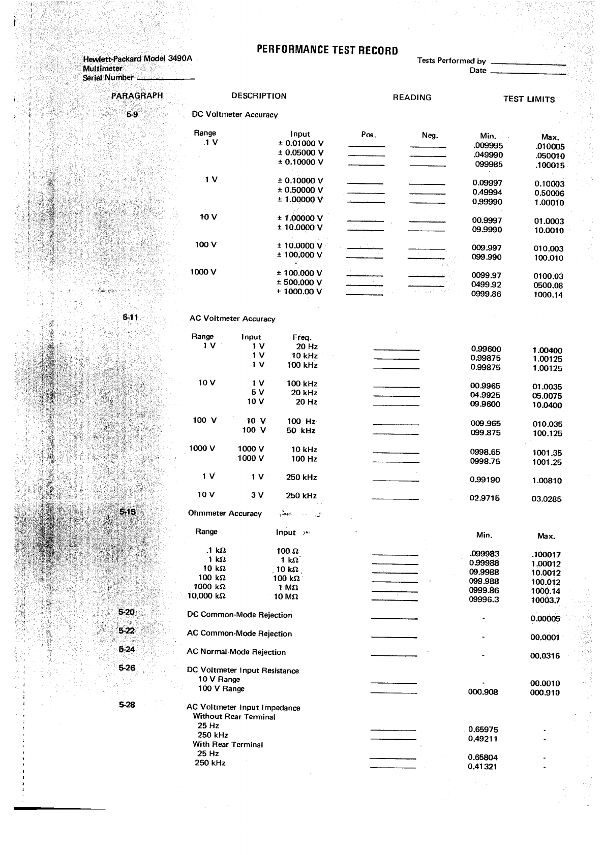
PERFOBMANCE
TEST
RECORD
. . Hewlett,-PaQkard
Model 349oA resrs
performed
by _
Serial
Number
PARAGRAPH DESCRIPTION READTNG
$9 DC Voltmeter
Accuracy
',
t',. ,..: .: ':;:..'',
TEST
LIMITS
.1
V 10.0100ov .009995
. r0.05000v .049990
0.99600
0.99875
0.99875
oo.9965
(X.9925
G).9600
o09.965
o99,875
0998.65
0998.75
0.99190
02'9715
Min.
.@9983
o99988
0{,.9s88
099.988
tr s9.86
09996.3
Max.
.010005
.050010
.100015
0.10003
o.50006
1.00010
01.oo03
10.0010
o10.o03
100.010
0100.03
0500.08
1000.14
1.00400
1.00125
't.00125
01.oo35
05.0075
10.0400
010.035
1@.125
1001
.35
1001
.25
1.OO810
03.0285
Max.
.1000t7
1.00012
10.0012
100.012
100o.14
100G'.7
0.00005
o0.0001
oo.0316
oo.0010
oo0.910
tV ro.100OOV 0.09997
.::i::..r:..,::.
:,-:..,:- 10V 11.0oooov oo.gggz
,r,,,,,.,. 110.O0OOV 0{1.9990
r 10o.00O
V 099.990
1OOOV iloo.ooov 0099.97
i 50O.00O
V
+ IOOO.OO
V 0999"86
stt AC Voltmeter Accuracy
Range
1V
10v 1V
5V
10v
lmo
v
1V
10v
1000
v
1000
v
1V
3V
I
nput
1V
1V
1V
Freq.
2O Hz
1O kHz
1fl) kHz
10O
kHz
2OkHz
2O Hz
10 kHz
1O0
Hz
25O
kHz
25O
kHz
. 10OV lOV lOOHz
tOO
V 50 kHz
'':;;
:'t:1 '
='t;!,' ,';,:
t.rtj:..::..::
..
:,:i;.,:,'
,',.,,'
';'t:',:'.,,',t.
Ohmmeter Accuracy
Range Input r.,
DC Common-Mode Rejection
AC Common-Mode Rejection
AC Normal-Mode Rejection
DC Voltmeter Input Resistance
1O
V Range
1O0
V Rangre
AC Voltmeter Input lmpedance
Without Rear Terminal
25 Hz
25O kHz
With Rear Terminal
25 Hz
250 kHz
000.908
0.65975
0.49211
o.65804
o.41321
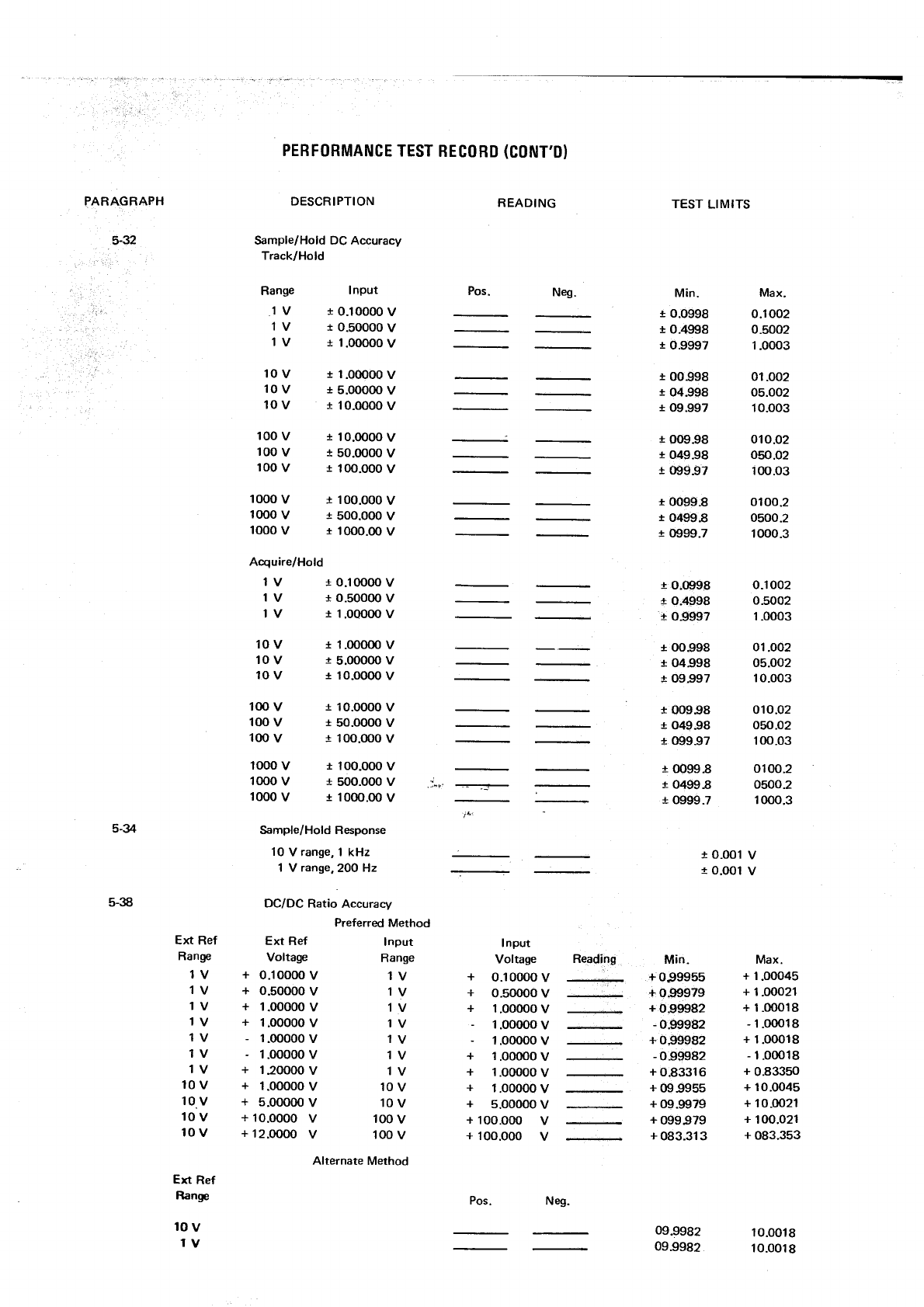
PERFORMANCE
TEST
BECORD
(CONT'D}
PARAGRAPH
5-32
DESCRIPTION
Sample/Hold DC Accuracy
Track/Hold
READING TEST
LIMITS
Range
1V
1V
1V
10v
10v
10v
100
v
100
v
100
v
1000
v
1000
v
1000
v
Acquire/Hold
1V
1V
1V
10v
10v
10v
100 v
100
v
100
v
1000
v
1000
v
1000
v
I nput
* 0.10000
v
r 0.50000
v
r 1.0oooo
v
r 1.00000
v
r 5.00000
v
I 10.oo00
v
r 10.0000
v
r 50.oo00
v
i 100.000
v
! 100.000
v
r 500.000
v
1 1000.00
v
r o.10000
v
1
0.50000
v
r 1.00000
v
r l.ff)Ooo
V
I 5.00000
v
! 10.oo(n
v
r 10.oo00
v
1 50.ooo0 v
1 100.ooo
v
r loo_ooo
v
I 50o.ooo v
r 10fi).00
v''a?.-:_
Min.
t 0.0998
r 0.4998
! 0.9997
r 00.998
r 04.998
r 09.997
r 009.98
r 049.98
r 099.97
r 0099.8
* 0499.8
r 0999.7
! 0.0998
+ 0.4998
r 0.9997
I 00.998
r 04.998
r 09.997
r oo998
r 049.98
t 09937
r OO99"8
! 0499-8
! 0999.7
Max.
0.1002
0.5002
1.0003
01
.o02
05.002
10.o03
010.02
o50.o2
100.03
oloo.2
0500.2
1000.3
o.1002
0.5002
1.0003
ol .o02
05.oo2
10.oo3
010.02
o50.o2
'too.03
0100.2
0500.2
1000.3
Pos. Neg.
5-34
5-38
Sample/Hold Response
10Vrange,l
kHz
1
V range,2OO
Hz
DC/DC
Ratio Accurary
Preferred Method
r 0.001
v
r 0.oo1
v
Ext Ref Ext Ref
Range Voltage
1V + 0.10000v
1V + 0.50000v
1V + 1.O0000v
1
V + 100000v
1V - 1.ü)O00v
1V - 1.00000v
1V + 120000v
10V + 1.0000OV
lO.V + 5.0OO0O
V
lOV +1O.O000
V
10v +12.OOO0
V
I
nput
Voltage
+ 0.10000
v
+ 0.50000 v
+ 1.00000
v
- 1.OO000
v
- 1.0qn0
v
+ 1.OO000
V
+ 1.00000
v
+ 1.00000
v
+ 5.00000
v
+
100.000 v
+ 100.000 v
-0.s9982 -
1.00018
+ 0.83316 + 0.83350
+ 099955 + 10.0045
+ 09.9979 + 10.0021
+ 099979 + 100.021
+083.31
3 +083.353
Input
Range
1V
1V
1V
1V
1V
1V
1V
10v
10v
100
v
100
v
Reading Min.
+099955
+ 0.99979
+ 0.99982
- 0.99982
+ 0.99982
09.9982
09.9982
Max.
+ 1.OO045
+ 1.OO021
+ 1.00018
-
1.OOO18
+ 1.00018
10.o018
10.0018
Ext Ref
Range
lov
1V
Alternate Method
Pos. Neg.
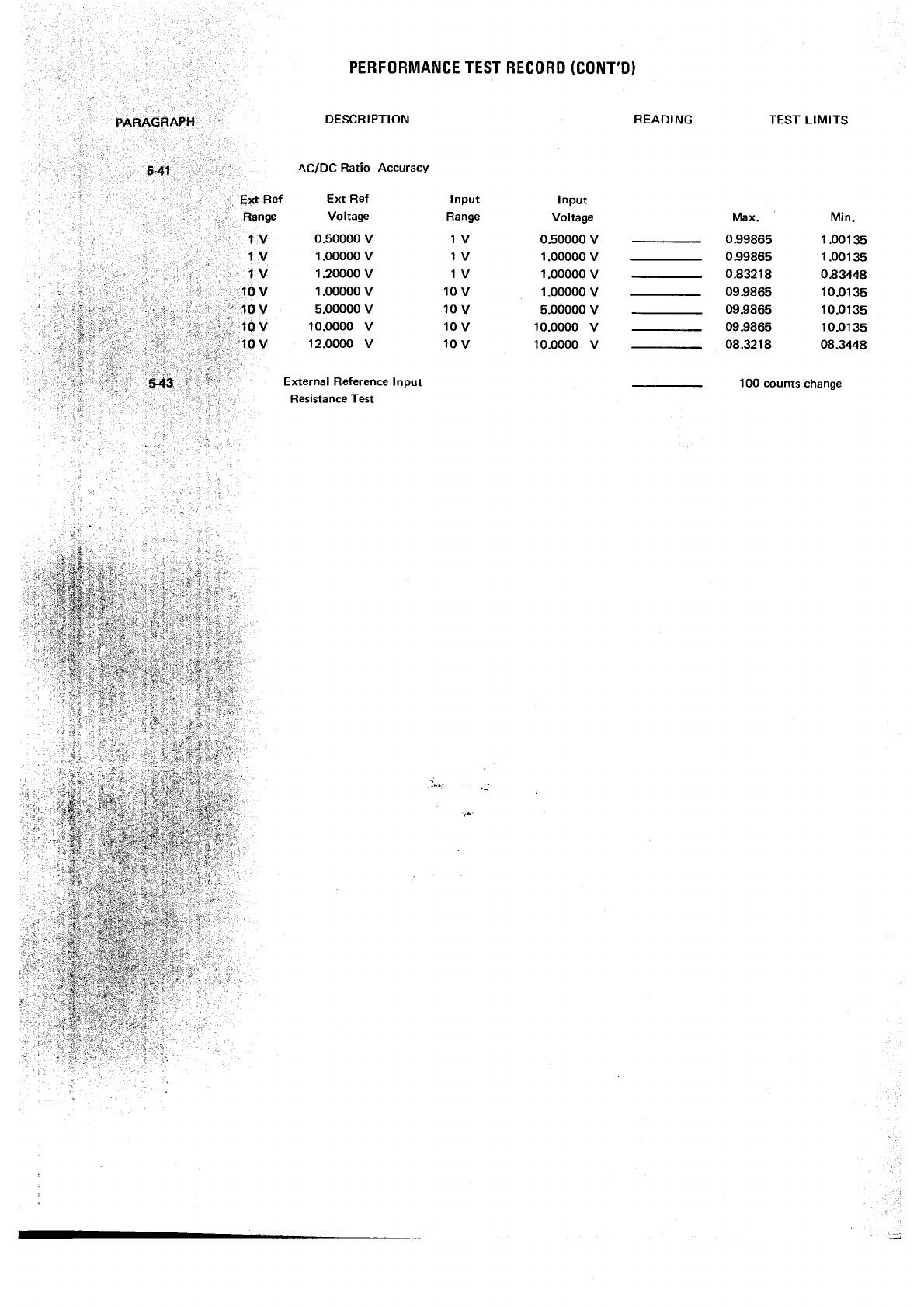
PERFORMANCE
TEST
RECORO
(CONT'D}
'^.:;^* DESCRIPTION
AC/DC
Ratio Accuracy
Ext Ref lnput
Voltage Range
READING TEST
LlMITS
.:. Ext
Ret
11;,',
F"ngu
, lV
' lv
: lV
-
10v
0.50000
v
t.ooooo v
120000
v
Max.
099865
099865
0.83218
099865
09.9865
09.9865
08.3218
Min.
1
.O0135
1.00135
0a344{l
10.0135
10.0135
10.o135
08.3448
1gv 1.00000 v
5.00000 v
10.ü)oo v
12.0000
v
External Reference
Input
Resistance Test
1V
IV
1V
t0v
10v
10v
10v
I
nput
Voltage
0.50000
v
1.00000
v
1.00000
v
1.00000
v
5.00000
v
10.o@o
v
10.0000
v
10O counts change
6-1.
INTBODUCTION.
6-2. This section
contains
information for ordering
replace-
ment pafts. Table
6-l lists parts in alphameric order of their
reference designators
and indicates the description, -hp-
part number of each part, together with any applicable
notes and provides
the following:
a. Total quantity used in the instrument (Qty column).
The total quantity of a part is given
the first time the part
number appears.
b. Description of the part. (See list of abbreviations
below.)
c. Typical manufacturer of the part in a five-digit code.
(See
Appendix A for list of manufacturers.)
d. Manufacturers
part number.
63. Miscellaneous
parts are listed at the end of Table
6-1.
6.4.
ORDERING INFORMATION.
6-5. To obtain replacement
parts, address order or inquiry
to your local Hewlett-Packard
Field Office. (See
Appendix
B for list of office locations.) Identify parts by their
Hewlett-Packard part numbers. Include instrument model
and serial
numbers.
6.6. NON.LISTED
PARTS.
6-7 . To obtain a part that is not listed,
include:
a. Instrument
model number.
b. Instrument serial number.
c. Description
of the part.
d. Function
and
location
ofthe part.
6.8.
PROPRIETARY
PARTS.
6-9. Items marked by a dagger (f) in the reference
designator
column are available
only for repair and service
of Hewlett-Packard
instrumenrs.
..........n€g6tiw tDsitive
zero
lz4o temrrature 6ef f icient)
-.. nan@cond{s} = lO-9
econds
...... notsp4acly repleable
Model
34904
sEcTt0N
vl
REPLACEABLE
PARTS
Section
VI
Ta.......
TC
. .... ..
,.. . ... .,optimum value
eletcd atfcbry.
@rage value *tom {pm may be mined}
... ... .. no
dildatd type numbc?
6i9ned
$lectgd d +ecial type
@ Dupont de Nemorc
sTD-A-2734
ABBREVIATIOilS
. . .
hertz {cyclelsl per sond) NPO . .
Hz.
tD.
rmpg inside diamet6
. . impregnated
..incande$ont
. in$larion{edl
dep.-
DPOT
OPST
@J..
c@f .
@dp
el4t
acap
FET
txd ..
rL
HR
J.
K.
L.
MP
P.
8.
c.
CR
OL
6
L........, ....inductq
lin,............. ..linedtapü
lo9.
.., ,. ... . . . logorithmic
tapd
mA .. . .. ., . .. milliampere{s}
= 1O3 amera
MHz
..............megahenz=
10+6here
Mll...............megohmlsl -
10+6ohms
retllm
..... .........retatjilm
mtr....... .,...mmuf*'tiiä
. . - .faradld
...... fieldeflet trilsistor
.........rixed
.........asmblv
. , . . . . . . . . . moto1
..........battery
........€pertor
.....
-
.....
daode
........&tay
line
. . ......,Emp
mis eletronic part
............
lu$
ms
mt9
yr
NC
Ne..
NO
. . nanoampere{s)
= 1O-9
a-oer*
.
... .. . normally
closd So . ., ..., .elenium
.neon *ct .......*ction(sl
normally
open Si ....., ......silicon
DESIGNATORS
. .filter O. .
.
.........hearer
OCR .........
integratedcircuit
8..,.........
...
....
iack RT
. .. .
. ..relay S
.....,ransi$q
- üansi$ordiode
........resisor
.....thermistor
.........sitch
.... trans{ormet
. . teiminal tE*d
...therrccouple
..-...tdpornt
......anductor
T.,
.....
... meter
TB.
rechani@l parl TC.
plug TP .
DECIMAL MULTIPLIERS
Pr.lix Symbols M0ltipli6 Pr.fix Symbok Multiplie
Eta
gr9
rpga
kilo
h&to
deka
deci
T
M or Meg
Kork
h
da
d
to12
to9
ro6
rd
t02
lo
1o-1
centi c 10-2
milli m tO-3
micro lI to€
nano n l0-9
pico p 10-12
femto t tO-15
afio a 19-18
6-l
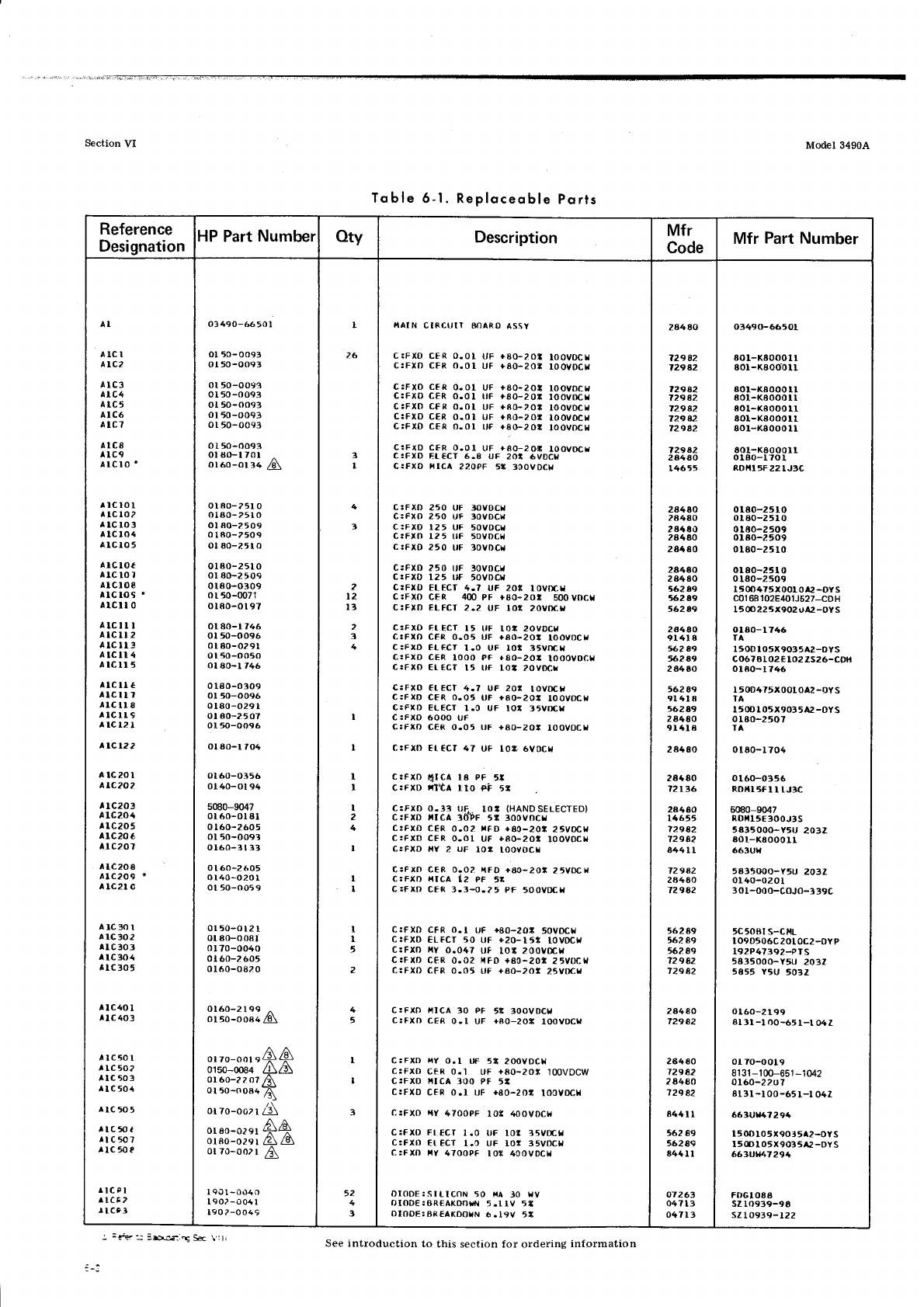
Section VI Model 3490A
Toble
6-1. Reploceqble
Ports
Reference
Designation
HP
Part
Number otv Description Mfr
Code Mfr Part
Number
AI
alcr
^tc2
^lc3
^tc4
alc5
alc6
alcT
alcS
Alc9
alclo'
^tclol
llclo2
Alclol
a
lc lo4
alclo5
alc lol
alc lo'l
alcloe
alclo9
alcll o
alcll I
alc ll 2
alcll.z
atcll4
a lcll5
alc
ll c
alcllT
Älc
ll I
A lcrr 9
Alcl2l
Atct2 2
alc20l
^1c202
a
1c203
alc204
Alc205
alc20 6
alc207
a
lc20 a
atc20
9
i lc2l c
arc30l
a Ic302
rlc303
A
lc 304
Ä
lc 305
atc40l
A
lc 403
Älc50l
r
lc
50?
llc503
llc504
alc505
llc50a
^1c507
llc50?
llc9l
rlcF2
rlcr3
O349O-{165Ol
ol 50-0093
ot 50-o093
ot 50-o093
ol 50-o093
oI 50-oo93
ol 50-oo93
ol 50-oo93
ol 50-o093
ol ao-l 7ot ^
or60-or34 lg\
ol80-2510
olao-251o
ol 80-2
509
0
I 80-?50
I
ol 80-251 0
ol 80-2
5t
o
ol 80-2
509
olao-o309
or 50-0071
o 180-o
I 97
ol ao-l 746
ol 50-o096
0l 80-0291
ol 50-oo50
ol ao-t t46
0
180-0309
ol 50-o096
o1.80-o29
I
ol 80-2507
or 50-0096
ol ao-l 704
ol 60-o356
ol 40-ol 94
5@0-9047
ol 60-ol I I
ol60-2605
ol 50-0093
ot60-31 f3
0 t 60-2605
or40-o20 I
ol 50-oo5 9
0t 50-ol2 I
ol ao-0 08
|
ol 70-0040
ol 60-2605
ol 60-082
0
ol60-2199 ^
ot to-ooe+ &\
or
ro-nnr r$$
0150_m84
/t\/3\
or oo-z
z
or
/\
ol 5o-ooB4-F
o,
to-oo, t Ä\
otan-oril 44
oteo-ozsr
Al{
orzo-oozr
$
l90l-o040
1902-o041
1902-0049
I
26
I
I
4
3
?
t2
l3
2
3
4
I
I
I
2
4
I
I
I
5
2
4
5
I
I
I
I
3
52
4
I
I{AIN
CIRC{III BOÄRO
ASSY
c:FxD CFR
o.0l UF
+8G-2ot loovDcr
c:FxD cFR O.0l uF +80-20t IooYDcf
c:FXD CFR
0-Ol UF +80-201 IOOYDCT'
c:FXD CER
O.01. uF +80-20t loovocH
c:FxD cFß o.0l uF +80-201 loovDcl{
c:FxD c€R o-01 uF 180-20t loovDct
C:FXO
CER O.Ol t,F +80-20: IOOVOCT{
c:FxD cER
O-01 uF +80-20* loovDcH
C:FXD
EL€CT 5.8 UF 20? 6VDC}'
C:FXD IIICA ?2OPF 5t 3oOVDC|{
c:FxD 250 UF 3oVDClt
C:FXD 250 UF 3oVDCtl
c:Fxo 125 UF 5oVDCY
c:FxD I25 UF 50VDClr
C:FXD
250 UF 3OVDCT
C:FXD 250 rrF 30VDC!
c:Fx0 125 rrF 'ovDct
C:FXD
ELECT
4.? UF 2OI IOVDCI
C:FXD CER 400
PF +80-2Ot 500VDCta
c:FxD ELFCT
2.2 UF tot 2oVOC||
c:FxD FTECT
l5 UF lot 2ovDct
csFxD cER O.05 rJF +AO-20t IOOVDCT
clFxD FLECT
1.0 t,F lot 3'vfr.H
c:FxD cER 1000 PF +80-20t looovocL
C:FXO ETECT
It trF lot 2OvDCr
C:FXO
ETECT
4-? UF 20t lovDcr
C:FxD CER O.05 UF +A0-2O: IOOVDCT
c:FxD ELECT
1.0 UF lO! 35VDCL
c:Fxo 6000 uF
CrFxD CER O.O5 UF +8O-?Ot IOOVOCt
c:FlD El€cr 47 UF lot.6VDClt
C:FXO
tllCA l8 PF 5t
c:FxD ifca lto +i 5t
C:FXO 0.33 t,F."
IOI (HANDSELECTED}
c:FxD rtc^ 30?F
5t 300vDcr
c:FXD C€R O.02 r.FD rAC-20t 25VOCta
C:FXD CFR
O.Ol trF +80-2Ot looVOCr
C:FXD
tlY 2 UF 10t IOOVDCI
c:FtD cER 0.02 {FD +a0-20t 25VD{r{
C:FXD HICA
12 PF 5X
c:FXO CFfr 1.34-25 PF 50oVDCr.
c:Fxtl cFR o.t (rF +ao-201 5ovDcI
clFxD €LFCT 50 ('F +20-l5i lOvDCr
C:FXD rY 0.047 rrF lot Zoovmx
c:FXD C€R
O.02 t{FD +80-?0t 25VDCl
c:FxD cFR O.05 [,F +80-20t 25YDC|.
c: FXD f,t
l ca 30 PF 5t 300v
octa
C:FXO
CER
0.1 UF +80-2Ol IOOVDC9
c:FxD rY o.l rF 5t 200vDcr
c:FxD cFR 0.1 trF +80-20t 1oovDcw
c:FxD t{lcA 300 PF 5t
C:FXD
CFR o.l trF +a0-2ot lO0VDCi
C:FXt t{Y
47OOPF
lOt 400VDCr.
c:Fxo Ft
EcT I .0 trF lot 35vmr
C:FXD
ETECT
1.0 UF 10t 35VDCI
c:FxD IY 4700PF
l0t 400vDCl
DIODE:StLICnN
50 ilA -10
t{v
DIOD€:BR€AKDO|,i'
5.IIV 5I
OIODE:AREAKDOTN
6.19V 51
28480
72982
729A2
129A2
72942
l29A2
72.r 82
t2942
72982
2A4AO
t4655
28480
24480
28{80
24440
28t80
24480
28480
562 89
249
562A9
2A480
91418
*249
5C,2A9
28480
56289
91418
56249
2 4480
91418
24480
28440
72t36
28480
t4655
729A2
729A2
84411
729a2
2a4AO
7?9a2
56249
5aa2 A9
56289
729A2
729A2
24480
72982
28480
72942
2 8480
729A2
84411
562A9
56?A9
84(tl
o7
263
o47ta
oaTl
3
o349(F66501
aol-Kaoool I
801-x800011
aol-K8000 ll
801-K80001
I
80
t-K8000 l1
801-K80001
I
801-K8000 1l
80t
-K800011
o180-l?o I
RDilI5F22IJ3C
olao-251 o
ol 80-2 51 0
o1.80-2509
olao-z509
o 180-25
IO
ol 80-25 I O
olao-2509
Itoo4TSXOOt
Ot2-OYS
c01 68
102E4,01J627-CDH
l5ü)225I9O2 r-lA2-OY S
otao-1746
rA
ItoD 1o5x9035A2-OYS
c0678l02E l02 ZS26-COH
ol80-1746
l50D475XOO1
0A2
-OYS
TA
1500 I 05 x9035a2
-oYs
o 180-250?
TA
o tao-l 704
ol6(F0356
RDXI5FIIIJ3C
5@0-9047
n oil15E
300J3S
5a35000-Y5u 2032
a0l-K8000 I I
663Ura
5835000-Y5u 2032
ot40-0201
301-ooo-coJo-339c
5C508I S-Cl,{-
t09D506C
20lOC2-OY
P
192P4739?-P
T
S
5835000-Y5u 2032
5055 Y5U 5032
ol60-2 I 99
8ltl-l00-65I-t 04z
or 70-ool9
8r 31
-1
00-651
-1042
ol60-2?u7
8t3l-loo-651-l 042
663Uta{7294
l5
00
to5
x90r512-DYs
l5o I o5
x9035A2-DY
S
663ttvr7291
Ffrcl088
sz 10939-98
sz
I
0939-122
r :ir-:e-:r-.Sa \':ti See introduction to this section for ordering information
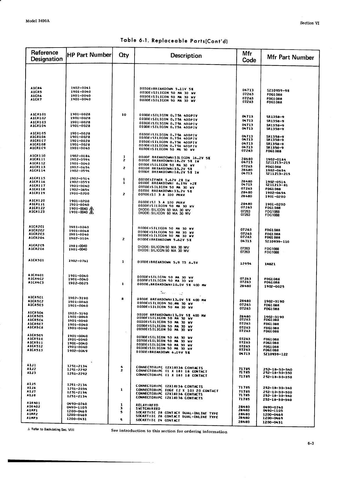
Model 34904 Section VI
Toble
6-1.
Reploceoble
portslCont'dl
Reference
DesignationHPPart
Number otv Description Mfr
Code Mfr Part
Number
AICR4
A
ICR5
AICR6
llcRT
alcßlol
llcRl02
alcRl03
alcRl04
a lcRl o5
alcR I 06
alcRr c7
A
tcRl o8
A
lcnl c9
alcRllo
alcßl I I
A
lcRt 12
AlcRl
l3
AlcRl 14
alcRl
l5
illcRl16
AlcRttT
AlcRl
l8
AlcRl19
irlc8l20
rlcRt il
llcRt22
alcßl?3
alcR20l
l lcR202
alcR2c3
alcR204
llcRz ct
AlcR206
AlcR30r
A
tcR40l
A
lcR{02
l tcßtc3
a lcntcl
/rlcR5C2
I lcR503
alcR504
alcR
505
alcRS
C6
l lcR5c7
^lcR5 08
AICR'G9
A
lcR5l0
AlcR5rl
rlcR5l2
llcRSl3
1902-o04 I
l90l-oo{o
t90l-oo40
leol-0040
I
90
l-0028
t90l-o02 8
190l-oo2 I
l90l-o02 8
190
l-o028
190
l-o02 I
190 t
-oo2a
I90l-o02 8
190
l-oo40
1902
-ot 84
1902-0
594
190
l-oo40
t902-o654
1902-O594
1902-o 5
I 4
1902-o55
9
190
t-oo+o
L902-0654
190
l-0200
l90l -0200
190
l-oo40
rcor-@4o
A
leol-m4o
l\
190
l-oo40
I 901-o040
190
l-o04()
1.902-3104
leo t-0040
190 t-q)40
1902-O76t
I
90
l-oo40
190l.-o040
t902-0o25
1902-3
t90
190
l-oo40
l90l-o(xo
t902-3 190
I 901-oo40
190
l-0o40
190
t-oo*o
190 l-oo40
t90 l-oo40
190l.-0o40
l90l-o(xo
190
l-oo40
1902-O049
t25t-2Lt4
l25t-?-292
t25t-2292
l25t-2tr..
I 25r-2034
r2 5l-2 I 34
l25t-2tt4
o{90-o740
o49(Fl lo 5
t20(F046 9
1200-o469
1200-o43 I
DIOD€:AR
EA(OOTx
DIOOE:SILICOT{
50
olooE:s tLICON 50
DI0DE:Stt-tCON
to
5.tly 5t
x foYV
ilA 30 ry
r|A 30 Lv
o4r13 | szrog,e-ee
07263 I FDGIOAs
07263 | FDGrOss
07261 | FDGlOss
I
2
DIOD€:SILICOil
O.7iA 4OOptv
OIOD€:Sl
tICora O.7iA 40Op
ty
DIODE:S
ILIC(IN O.7ilr 4OOptV
DIOoE:SILICON
O.ZiA 4OOptV
DIODE:SIf
IcoN o.7tA 4ooPIY
oloDE:
Sil-ICoN o.7i
4oopIv
DIoDE:S
ILICON
0.75A 4OopIv
OIr|{)E
:-SILtCON
O.?
iA 40Op tV
otoD€:slLtcor{ 50 t4A
,o rv
DtooF SRFAKDOUü{:StL
lAnN 16.2V
DtoDE SREAXDOTN:18.2V
5t lt
OIODE:SILICOil iO ||l lio ray
oIooE BREAT(DOttr:33.2v
5t
Ot{lo€ SRF^KOOLit:la.2V
5t lt
oIoD€:zFNER
5.62V 2' tu
Dloo€ BREAT(DOHil:
6.19V +2t
DInDEISILICO}{
iO x fO By
OIOD€
BREAKDOTa{i
f 3.2V 5t
DIOOETS
I :l r IOO pR.Ry
DIODE:SI3AIOOPRRY
DtoDE:Sil-ICOr{ 50 ilA 30 tv
DIODE:
SILICON
50 MA 30 Wv
DIODE:
SILICON
50 MA 30 wv
ot? 13
0+713
o47t3
o{713
or7l3
otTl:l
oa?13
04713
07 263
24480
o4?13
07263
284eO
o4713
2A4AO
o47tt
o726t
2a480
2a4ao
2a4AO
o7
26t
07263
07263
sRl35a-9
sRl35a-9
snl35a-9
sRl35A-9
sRl35a-9
sR1358-9
sRl3ta-9
sR
1350-9
FD6l OAa
1902-0184
sz
lt 2t3-2lt
FOGI
O8A
1902-0654
szIl2t3-215
1902{r514
szll2l:Fal
FO€tO8A
1902{t65a
l90l -o200
l90t{)200
FOGI
OAA
FDGl(88
FDG1O88
DtoDE:SIttCOtt 50 lt^ 3{!
oloD€!sILICOlt 50 ta 30
otoDE:sILtco|| 50 x 30
DIoDE:AREAXO0Iil
5.62V
TY
tv
LY
5l
07261 | FDGlOrs
ot26r I toeroes
of26t I FDGlOss
04713 | Szro939-l lO
DIODE:
SILICON
50 MA
DIODE:
SILICON
50 MA a) wv
30
wv 07263 | FDG|@8
07?s,3 l FDG1@8
D IODE:8R€A(DO|.N 1295a lNa2l
DloD€:sttIcoN 50 lt :x)
DIDDE:Slt-ICoN
50 nA 30
DlooE
r
Bt.
EA|(DOft{:
I O-oY
UV
YY
51 400 ralt
o7263 | FDclosS
o726t I FD6lo88
28480 | l9o2-O025
DtooF SREAKOOTI:13.ov
5t {ü)
DIOD€3Sn-ICOli
50;tl 3o rY
DIODE:SILICOI 50 fl f,O rV
26a80
o7263
o726t
2A4AO
o7 26t
07263
o1267
o7263
o726t
o7263
of26?
ot263
ot7l3
7t785
TLTA'
7l ?85
7t7A5
7t7A5
7t 785
t1785
2alr80
2A4aO
28480
28a80
28+60
1902-31
90
FDGI
OA8
FoGloaa
1902-31
90
FD6tOSA
FD6l OA8
FDGI
OAA
FD6lOSA
FO6loaa
FDGI
088
FOGlOSs
F06lOES
sz
10939- 122
252-t8-3(F340
2t2-ta-to-tro
252-ta-to-t50
252- le-t{F3to
252-t(F3o-300
2tlla-3{F3t{t
252-lE-30-3ro
oa9(H7to
0490-ll05
1200-0469
12(}0-0+69
1200-{)43l
DtooE ERFIXDO|N:
l3.ov
otooE:sILIcoN 50 l{a 3D
DIODE:SILICON
5O xA 30
DIOOE3SI|"ICON
to t|^ 30
DtoDE:Sil-tCOX tO r :ro
DIOOE:SILICOI{
50 ||A 30
DtnDESSILICON
50 t| 30
DIODE:StLtCOr{
to tA 30
DIODE:SILtCOt{
50 H :o
OtoOE:EREAKDO$|
6.19y
5t aoo tr
t|Y
IY
tv
lv
HV
tv
yv
IY
,a
AIJI
l lJ2
AIJ
3
CONN€CTOR:
PC
CONNECTOR:9C
C{}INECTOt:PC
COilNECTOR: PC
carilNEcroR:Pc
coililEcroR: pc
C(x{NECTOR:PC
REI-AY:
RE Et)
S IITCH: R€ED
S(f,KEr: lC 28
SOCI,FT:lC
2E
S(tr(El:lC 24
t2xl8t36 cOXTICTS
ll x lat la c(ltTAcT
tl x lat la c{tlT^cl
lzxl8t36 CONTACTS
EDGE
t2 X lot 20 coNTACr
l2xl8t36 COI{TICTS
t2xlat36 coilrf,Ts
coraTAcr DUAL-ll{tntE IYPE
CONTICI DU L-II'LtiIE TYPE
colrlcr
/rlJ5
tlJ6
lJ7
AtJ6
lrao I
r lxao 2
l ltPl
l lrP2
l ltP3
I
I
t
l RE er to &ckdating Se. Vltl See introduction to this section for ordering information
6-3
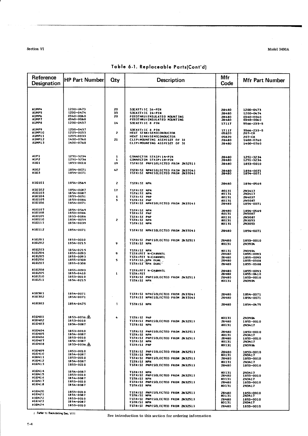
Section VI ModeI 3490A
Tqble
6-1. Reploceoble
Porls(Cont'd)
Reference
DesignationHP Part Numbel oty Description Mfr
Code Mfr Part Number
AlPl
^tP2
alol
AlflPa
rl||PS
l liP6
tlfiP?
A
ITPS
l lltP9
altlPlo
ll||pll
^l||Pl2
a
lxPl 3
^lo2
Alo3
a lolol
^
lo lo2
rlo lo3
A lo lo4
llo lo5
a
lo loe
aloloT
Alotoa
llo lo9
alollc
aloll I
loll2
a
lo20 I
^to202
I to203
Alo?o4
ll o20
5
rIo20€
llo20 7
l 1o208
llo209
tlo 2lo
llo2lt
r lo30 I
A
lo 302
llo303
llo40 I
Alo4('2
llo403
^lo{o4
alo4()5
^
loao6
llo{o?
llo40 8
Aloao9
ll.o {l c
llo{l I
r lo4l 2
l lg4l 3
llo4l4
r lo{15
lloat a
l lo4l 7
llo{l I
/r
lO42O
llo42 I
^ lo{2 2
rlc423
r 1042.
1200-0473
1200-o4?4
0340-o060
0340-o050
1200-o4_t?
1200-o{!t 7
12{)5-o03:l
l20Foo33
1400-o?60
l{oo-o760
L2tl-7231
t2rL-1236
l8 5i-ool o
1854-OO7
I
1854-OO7 I
l8q-0569
1854-OOa7
l8 5a-ooa7
la 5t-oo5r
l8 53-OOa6
la54-oo? I
la54-o569
la 53-oo86
l8 53*0086
I A5{-O03 9
l8 54-OO19
I 854-OO7
I
I I 53-OO
lO
185+-O2l 5
l8 54-O2l 5
la55-o093
la55-o(xr 3
1855-OtO8
r855-O308
1855-O09t
1855-O4lO
l8 53-OOl O
l8 54-02 I 5
t85+-OO7
I
t8
54-OO7
I
ta'1-0475
ra sloora A
l8 53-OO
lO
1854-OOA?
l8 5l-oo lo
1854-OOa7
185t-oolo
185+-O08?
ra:r-ooae 7$
I
853-OOl
O
l8 54-0087
1853-OOIO
Ir54-OOa7
I 853-OOt
O
la54-ooa7
I
853-OOl
O
Ir 5+-OOA
7
r r53-ool o
Ir 54-OOA
7
la5:t-ool o
It54-OOa7
l8
53-OOl
O
l8 9a-ooe7
l8 53-OOl
O
20
t7
20
14
2
2t
I
I
I9
47
2
t7
I
5
2
9
9
5
I
1
^tttoll
S(f,,XET: lC l6-PlN
soc(ET: lc l4-Pta{
FEEOTHRU
: IilSULATEO X(l.lNT IilG
FEEDT}NU: INSI'LATEO Tfl.|'{TING
S'trKET: IC 8 PIN
SMKFI:IC 8 PIN
H€AT SI N(:SEtlICOil{XrCToR
HFAT SI XK:SETICOI{ü,CTOR
CLIP:I{flJilTING ASSYISE OF
CLIP:l{(]u||rlNG ASSY(S€I OF
3l
3l
CONNECTnR
SIRIP: l4-PIt{
CONNFCTOR
STRIP: I8-PIil
TSrR:St PilPTSELECTEO
FRof{
2il3251|
rsTR,:st itptilsELECTED
FROI{
ät370+l
TSfR:Sl IPNISEL€CrEO
FROx
2N17O4l
TSTR:SI NPN
TSTR:SI NPI{
TSTN,:ST NPN
TSTR:ST PilP
TSTN,:ST PNP
TSTß:SI NPNISFI.FCIED FROII
TSTR: S I IiIPN
TSTR:SI PI{P
ISTR!SI PNP
rSTR:SI NPN
TSTR:SI NPil
rSTR.:SI NPilISELECTED FRol| an 3?o4
|
TSTR:SI PNPISEt€CTEO FROr ?'tt2Stl
TSTß.: Sl tilPil
ISTR:SI NPII
ISTR:FET N-CHANNEL
ISTR:FET N{HAXilEI
rSTR:SI- NPil DUAL
TSTR:SI ilPil OUA[-
TSTR:FFT iHI{.IINEL
TSTR: F€I
rSTR:SI PNPIS€l-€CTED FROI 2it325t I
rSTR:SI NPiI
ISTR:SI NPN(S€LECTED FROI{ 2N:}?O4I
rSTR,:Sl xPN(SELECTFD FRox ät3704l
TSTR:SI NPN
TSTR: SI PNP
TSTR:SI PNPISEI-€CrEO
TSl8.3SI llPN
TSf R,:
SI P}'PISEL€CTED
TSTR:SI NPT
TSTR:SI PiIPISETECfEO
TSIR:Sl taPN
fSfR:Sl Pl{P
ISTR:SI PNPISELECTEO
fSTR:Sl IP||
TSIR:SI PilPISELECT€O
ISTR!Sl tlPN
ISTR:ST PilP(SELECTED
TSTR:SI NP'{
TSTR:SI Pl{P.SELECfEo
TSIR:SI IPri
rsrR:st PlrPts€LEcTEo
tSlR:SI NPa{
lSTL:Sl PllPlS€LECIED
TSIR3Sl liPN
TSTR:SI PiIPISELECTED
rSTR:SI TPX
fSrR:Sl PttP{SEtECTEO
FROil at325l )
Fn,ot är325t l
FRO|( ä{ 325t t
FROX 2it325l I
FROil är325ll
FROI|
2N3251I
FROft 2X3251
I
FROil 2r{3251
t
FROX
at325lt
FROX
ar3251t
FROI at325l I
24a80
24480
26t60
28460
l7ll7
lTll?
05820
05am
2AlAO
28+AO
28480
?alao
2A480
28480
2e4AO
2A4aO
80t 3l
8013t
ool 3l
aol3l
2raeo
2E4AO
801 3l
aot3l
801 3l
aol 3l
23tao
28tAO
80t31
aoI3t
28aao
264AO
24480
2A4aO
2a480
2a{ao
28480
80131
2AtAO
28aAO
28aao
8013t
28tAO
aol3 1
2A4AO
aol 3l
2AaOO
801 3l
80131
28t80
EOl3l
2A{80
80131
2A480
ao l3l
28{80
ro
l3l
2e480
a0l3l
2E480
aol3l
2Atao
8{tl3l
26tAO
t2OO-O473
120(F()t74
0340-o060
o3a(Foo60
,56-23t-5
t'66-235-5
2O7-CB
207-CB
1400-0760
l4(xFo760
t25t-t2ta
L25t-:Jzt6
ta53-oolo
la54-oo7l
l85t-OO7 I
la54-0569
2||tltr
2lt34l7
2N40t7
2t5047
184-O07l
1.854-0569
zil5087
2r5047
2N1053
2il3053
1854-OO?l
la5:Foolo
2N390+
2N3904
1655-0()93
r855-O093
1855-0308
1855-0308
1855-OO93
la55-o+10
lo53-o0 lo
2N3904
laSa-oo7 I
I A5a-OO7l
I A5.r-O47t
zil4906
I 853-OOl
O
2Nj,4t7
I 853{)Ol 0
2N341?
1853-OOIO
2r|:r4r7
2N3906
1853-OOIO
2N341?
1853-OOtO
2il!r417
t853-OO10
2N34r?
1853-OOtO
2N3417
1853-OOl
O
2N3417
la53-oolo
2N341?
la53-ooto
2il3417
1853-OOIO
€ -.!
: itt b R+.htiql Se Vill See introduction to this s€ction for ordering information
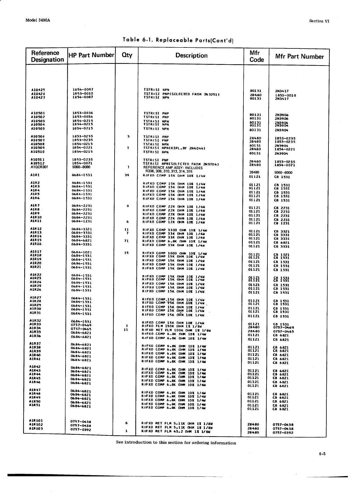
Model 34904 Section Vl
Toble
6-1.
Reploceoble
Ports(Conr'dI
Reference
DesignationHP
Part
Numbet atv Description Mfr
Code Mfr Part
Number
Alo42t
Aloa26
^to127
A
lo50 |
^to50?
llo503
llo50a
alo505
Alo506
rlo50?
A 1o508
llo509
a
loSt 0
^lo5ll
llo5l2
A10CR301
alßl
A
IR2
l lR3
^lßa
Ä
lR5
AlR6
ltR ?
llnS
llß9
rte lo
llRll
alt t2
llR l3
^lß la
rlR l5
rtR16
tlRlT
a
lnla
llRl9
AIR20
llß21
AtR22
rlR23
a
ln2a
ltR25
AlR26
alß27
AIR28
AIR29
AIR
30
llR3l
rlR32
tlR13
IIRH
tlR35
rlR36
AIR37
llß38
^1R39
^IR40
AIR'I
AIR+2
tlßa3
aln{a
llr45
rlt{6
rlta?
^lRa€
rtt49
tlt50
lln 5l
llt lo!
rll to2
llnlo3
l8 54-O087
l8 t3-oo lo
r854-O087
1853-OO:t6
l8 53-0036
ta54-o2t5
l8 54-02l 5
l8 54-02 I 5
tESt-o24,
ta5r-o235
1854-02l 5
ta54-o221
la54-02 t 5
L85t-O2t5
1854-OO7 I
5060-60d)
()6a4-l 53
I
06a{-l 531
o6a4-l 531
0684-1 53 I
0684- I 53 r
0684-1 53 r
06A4-22t1
06a4-??31
o6a4-2211
068/.-2231
o6a4- l23l
06a4-332 I
(}6a4-3331
0684-3331
06a4-6821
06a4-333 I
0684-lO2 r
0684-l 531
o6aa-l 53r
0684-l 531
0684- I 5:|l
0684-l 531
06a4-l 53
I
06a4-l 53 I
o6a4-l 53
I
06a4-l 53
I
0684-l 'f, I
068+-1 53
I
0684-l t:rl
068(-l 511
o6a4-l 53
I
{)6a+-1531
075?-O469
0757-Oa65
0684-6A2t
0684-6A21
0684-682 r
(}6a4-6A2 I
0684-6a2t
0584-682 I
o6a4-682 I
068t-682 I
06a{-682 I
o6a4-682 I
068+-6a2 I
o6a4-5A2 I
058a-6a2 [
068+-6E21
06aa-6821
0684-6A21
o6a4-6821
o?5?-O+3a
o7t7-(l438
o75?-o:t92
3
I
I
39
9
6
tl
7
7l
I5
I
ll
6
I
TSTR:
SI NPl{
fSTR:Sl PitPlS€L€CTED
FROü
ä{32i1 t
TSTR;SI NPN
ISTR:SI PNP
TSIR: SI P'{P
TSIR:SI NPiI
lSfRrSl NPN
TSTRsSI NPN
TSTR:SI PNP
fSfR:Sl PilP
TSTR:Sl NPN
ISTR:SI NPN(REPL.8Y
2N4O44I
TSTR:
SI NPil
TSTR:
SI P'IP
TSIR:SI NPiltSELFCTEO
FROI|
2fl170+l
REFERENCE
AMP
ASSY:
INCLUDES
R306,
3@, 310,
313,314.
315
R:FXD
CO'4P
l5K OHt{
tof l/4ta
R:FXD
COIP 15|( OHr{
lot l.r4l
R:FXD
COXP
l5K OHt lot l/4ta
R:FXD COt'tP
lt|( oHt| lot l/4r
ß:FXD COXP
l5t( (I{t lot l/41
R:FXO
CnfiP I'K OHr|
lot l/4r
R:FXD
COIP 22K Ot{t1
lot l/41
R:FXO COI.P
22t( OHfi lot t/4t{
R:FXD COIiP 22r OHfi toz lt4u
R:FtO COIiP
22|( OHt| LOt tt4Y
R:FXD
COXP
l2K (}tt lot t/{l
R:FXD COXP :l3OO
Olit tol l/{f
R:FXO
CO,.P
3:tt oHlt lot 1/4r
R:FXD
COXP 33R OHI{
tot l/4tl
R:FXD COnP 6.8K Olil rot l/4|a
R3FXD
COdP
33X OHr roa l/+l
R:FXD COftP
tooo otta loa Llt*l
R:FXD CO,|P ltt( OHt{ tor tt4t
RIFXO COtlP l5K OHat
LOt l/{r
R:FXD
COtaP
l5K oHlt lot l/41
R:FXD COiP I't( OHra
lot l/4r
R:FID COI|P
tt( OHt lot l/4r
R:FID COtaP
I'X OHtr lot l/4|.
RsFXO
COftP
I'K OHfl IOZ tl4|/
R:FXD
COHP
15l( OHfa
lor 1/4I
R:FXD
COXP l5K OHX
lot l/4r
R:FXO
COrP-I5|( oltx lot l/4U
R:FX0 CO,iP
tt|( OHX.lA! l/41
R:FXD
COXP
l5K OH)t
tot l/41
R:FIO COIiP
I'R OHrl 10t t/4t
R:FXD
coxp rtr olr"l lol t/tr
R:FXD
COrP I'K OHX
lol l/41
R:FXO
Ft-ft l50K oHfi tt l/81
R:FIO tl€T FLX loo(. Olil It l/ar
RIFXO COraP
6-at( ottt tot l/4r
R:FXD
CorlP 6.8{'O}fa lO: l/ir
R:FXD CO||P 6.E{ Orit lo: l/{l
R:FXD COI|P 6-8( Ol|| lot l/4r
R:FXD C0rap 6.a( o}[ lot l/{ta
R:FIO CO,iP 6.8( Ottt lot l/ar
R:FID COre 6.ax oilt lo! l/4ra
R:FIO COI|P
6.8( Olft tot ttry
R:FXD COI{P
6.8K Oln lot l/al
R:FXD Cotap
6.8X Olfi lot l/41
R:FXD COttP
6.8( Ottl lot l/tl
R:FXD CO,.P 6.AK Olft loa l/at
R:FXO COiP 6.8t( O}}t tot Llil
R:FXD CO||P 6.8{ o}|l l0: l/4tt
R:FXO COraP
6.8( Olil lO: l/4t
R3FXD
COtrP
6.8( Otft 10t l/4t
R:FXD COraP
6.8X Oltt IOt t/{l
R:FXO ilET Fl_ft
5-llx Otr lt lr8ta
R:FXD rFT FL,t 5.llx {Hx lt t.r8l
R:FID iET FLra
T3.2 olt lt t/8t
aol3l
28tAO
aol 3l
ao13l
80 l3l
80l3l
80131
aol3l
2A4AO
24480
801
tl
2a480
60131
2A4AO
28480
28'l8O
oll2l
oll2l
oll2l
oll2l
olt 2l
oll2l
ol
l2l
ol l2l
ol l2l
oll2r
ol
l2l
oll2l
oll2l
or l2l
oll2l
oll2l
0rr2l
ol t2r
ol
l2l
orl2l
olr2l
ot l2l
oll2l
ol l2l
oll2r
0rl2l
OII2I
oLI21
olI2l
0tl2r
01l2l
oll2l
2A480
28460
oll2l
ol l2l
oll2l
ol l2l
orl2l
or
l2l
ot t2l
oll2l
ol l2l
ol l2 r.
olt2l
ol 121
oll2l
oll2r
oLl2l
otl2l
otl2r
28680
2g4AO
2A4EO
2tt34l?
1853-OOl.O
2N34t7
ztrrt906
?N3906
2N39()4
2N3904
2l{390a
LASt-O2t5
I 853-023 5
2N3904
l8*-o2zl
zilt904
la't-ozr5
I854-OO7l
5060-6(D0
c8 l53l
c8
c8
c8
ca
c8
CE
CE
CB
CB
ca
ca
CB
ca
CE
c8
c8
CE
CB
CA
CB
ca
ca
co
c8
ci
I
531
I 531
I 531
I 531
r t3r
2?al
2231
22tl
2ztl
t?3t
3t2l
3331
3331
6a2l
333t
I
02l
l5tt
I 531
l53l
I 5:rl
I t3l
I 5:t1
lStl
I 531
lt3t
I t3l
t 531
I t3l
l53l
I 531
6821
6AZl
6A2l
6A2L
6 821
6g2l
682
I
682t
6821
5A2l
6A2l
6A2l
6A2l
6621
642 I
ot57-o438
o?57-O+38
otSt-or92
c8 lt3l
o757-0+69
o7r7-{J46'
ca 6a2l
c8 6821
CB
CB
c8
ca
c8
ca
c8
c8
ca
ca
CE
c8
c8
ca
C8
c8
ca
c8
CB
cs
See introduction to this section for ordering information
6-5
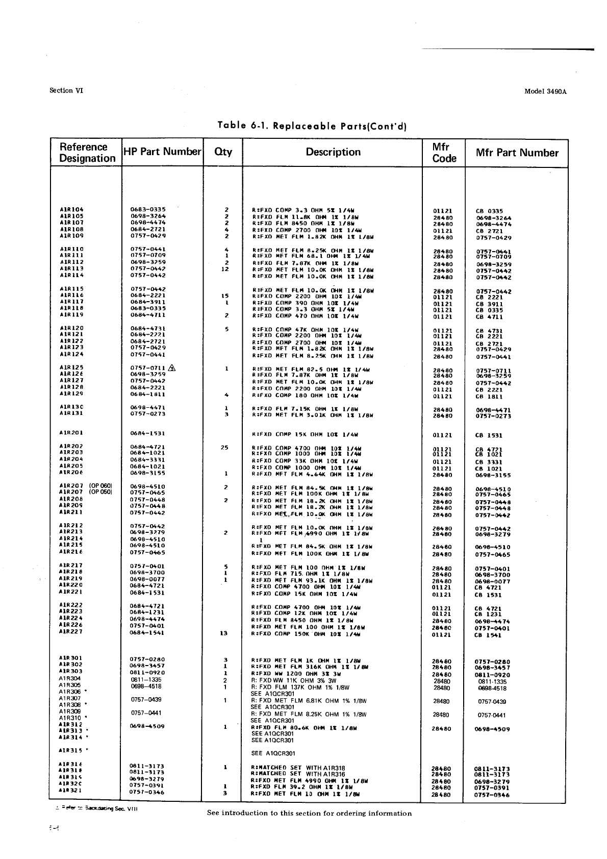
Section VI
: :+t 3 i*d{nE sa vlll see introduction to this section for orderins information
Model 3490A
Toble
6-1.
Reploceoble
Ports{Cont'df
Reference
Designation
HP Part Number Qty Description Mfr
Code Mfr Part Number
alR
l04
Ä
lt lo5
alR
lo7
alR
to8
alR
l09
alRIto
alR
ll I
alR
ll 2
alRll3
Älß
ll4
alßll5
rlRlle
AIR
II ?
alRll I
alR
lt9
llRl20
alRl2l
ltr 122
alR123
AIR
121
alR12t
^lR
12 6
atR127
!lR
128
A
lR 129
AIRI3C
alRl3l
alR20
I
a
lR 202
rlR203
r lR 204
alR
20 5
AIR20C
Ä1R20
7
AIR20?
^
lR 208
alR209
AlR2Ll
a
lR2l 2
AlR2l
3
a
lR2l {
AIR
215
alR2l
6
ÄlR2l7
Ä
lR2l
8
A
lR 2t9
AlR22
0
^lR?2
I
^tR222
^t9.221
alR22
4
A
lR 226
^IR22
7
arR
30
I
alR302
AlR303
Al R304
At R305
A1 R36
A1 R307
AI R3A
A'IR3@
A'tR310
^n3li
lln3r3
^
lR3l4
^lP3l5
lla3lG
llFSlt
^lt 3l
9
r
lt 32c
rlrt:l
toP 0601
(oP 0501
0683-O335
069A-3264
o69A-4474
o6a4-2721
o757-O429
o75Z-O44t
o757-0709
0698-32
59
o757-O44?
o757-0442
o757 -O4+2
06a4-2221
06a4-191 I
0683-O335
o6a4-4ll I
0684-4731
06a4-2221
o6a4-2721
0757-O429
0757-O441
o757-07t I
069A-3259
0757-M42
06a4-2221
06
a4-l al I
069A-447 1
0757-O271
0684-l 53
I
0184-472L
o6a4-lo2 I
0684-33?
I
0684-
I O2
I
069a-3t55
069A-45
t O
0757-U+65
0757-O448
0757- O+4
8
o7t7-o442
o75l-u42
0598-3?79
0698-451O
0698-451 O
o?57-0465
075 7-0401
0698-3?OO
0698-0O77
o6a4-472L
0684-l 53
I
0684-472 I
06a4-l 23
I
o698-4474
o?57-0401
o68t-l 541
o757-02a
0
069a-i457
oal l-o92 0
0Bl1-13(}5
0698-451
I
0757-@39
0757-0441
0698-4509
oSll-ar73
oStl-tl7f
698-3219
075?-039
I
07
5t-o3a6
A
2
2
2
4
2
1
I
2
l2
I5
t
?
5
t
I
I
25
I
3
I
2
2
2
l3
?
I
I
2
1
1
I
I
I
3
n,:FXO
COflP 3.3 OHil 5l tl4y
R:FXD FLll ll-aK Ot|I lt l/8t{
R:FXO
FLX Aa5O
OHll lt r/8r
R:FID Cof{p 2700 olri lot l/4t
R:FXO HEI FLir 1.82X OHil lt l/al.
RIFXD ü€r FLI 8.25t( (Hä lt l/aU
R:FXO XFT FLf{ 68.I Orfi l: l/4ta
R:FXO FLr't
7.87K Ol*{ lt l/8r
R:FXO nFT FLX Lo.O( OHl,t
M/8tl
R:FXD X€T F(H lo.OK O.tft
lt l/aH
R:FXD ri€t FLat
IO.O( (}ttl 1! l/8r
R:FXD COI{P
2200 oHft lot t/41
R:FrD COtp !t90 0Hll lot l/4H
RIFXD COtaP 3.f OHlr 5Z Ltl|t
R:FXO COrP 4?O OHtl
lot l/41
R:FXO
Cnt|P
47K OHx lot I/4t{
R:FXO
CO,|P 2200 ol$t lo: t/41
R:FXO COXP
2700 0tt1 lot t/4ta
n:FXD rFT FLfi l.8a( (}{t.t
lt t/Ar
R:FXD
ttET FLlt 8.21( r}tH lt l/81
R:FXO XET FLX 82-5 ollt lt l/41
R:FXO FLX
7.87K OHI lt l/8r
R:FXD lt€T Ft_r1
lO.O( OHn lt l/81
R:FXD
Co||P 2200 OHra
lO! 1/41
R;f.xD coHP lao oHt{ lot l/4r
R:FXD FLü 7.15K Ot{t{
ll l,/8t
R:FXD XEI FLt 3.01K OHI lt r/8H
R:FXD
COIP
l5K OHt lot l/4ta
RIFXD CO|,IP
47OO Ofrt tot l/{r
R:FXn COHP
lOO0 01ff lot l/41
R:FXD
CO|{P
13K OHt lot l/4||
R:FXD COttP
IOOO
Oftt lot lltaa
R:FXD ftFT Ftx 4.64{ r}tfa lt l/8r{
R:FXO nET FLX 84.'( fX.tt lt l/8r
R:FXO
r,r€T
FLX loOK OHX
l: l/81
ß:FID rtEr Fl
ü la. A( (xtr tt 1/8r,
R:FXD
||ET Ft_ä
la.z< ot{fi lt l/8r
R:FXO N€A,"FL| lo._o( o{}l tt l/sr
R:FXD
ilET FtX 10.0( oHft lt l/8tl
R:FXD lilFf FtX..{t9O OHX lt lr'8l.
t
R:FXO il€T FLt 84.5X OHil lt l/81
R:FXO
XFT FLft IOOK OHfl lt l/Et
RIFXO t{€T FLI IOO O]tr{
lt t/8r
RIFXO
FLt 715. OHt(
tt l/81
R:FX[ fi€f FLX 93.IK OHtt l? l/8il
R:FXD COf{P
ITOO Ol+l lot l/.rl
R:FXO
COIIP
l't( OHt lot l./4X
R:FXO COI{P
4700 0rS{ rot l,r4ra
RiFXD COXP
l2X OHt lot l/41
R:FXD
FtH 8450 oHH It l/8r
R:FXO
tET FLfl IOO OHH lt l/8ta
R:FXD
COIP I50K'Ol$t toz Lt41
RIFIO nET FLt lK (){r lt l/Or
R3FXD ltET FLr 3l6K Ot{t{
lt l/Er
R:FXD
ty l?OO OHll
3t 3ta
R: FXDWW
llK OHIM 3% 3W
R: FXD FLM
137K
OHM 1%
l/8W
sEE 410CR301
R: FXD iilET FLM 6.81K
OHM 1% 1/8W
sEE AlOCR3oI
R:
FXD MET FLM 8.25K OHM 1%
l/8\ry
sEE A10CR301
R:FXO
FLä 80.6K Olil lt l/El
sEE
A10CR301
sEE
A10CR301
sEE A10CR301
R:IIATCHED
S€T WITH
A1R318
R:IiATCHED
SET WITH
A1R316
R:FXO tET FLt +990 olf,t l! t/8r
RrFXD FLr 39.2 OHr{ tt ttSU
R:FXD
ft€T FL|l
l0 (HI l./0a
ol l2l
28480
284A0
ol
t2l
28480
28480
284€O
28+80
28480
28480
28480
oll2l
01
121
ol l2l.
oll2l
oll2l
oI I2l.
otl2r
28480
28480
2A4AO
24180
2A4gO
0rl2l
ort2l
28480
24t60
olL2l
oll?r
ol l2l
oll2l
olt2l
28480
24480
28480
28480
2A4AO
28480
28480
2a4AO
28480
2A4EO
28480
2A4AO
28+80
otl2l
oll2l
olL2l
ol l2l
28480
28+80
oll2l
28400
28t80
2A480
28480
2a4a0
28480
284f,0
28480
2A+AO
28480
28480
28480
28{80
cB 0335
0698-3264
o69a-4474
c6 2721
o757-O429
o?57-0441
o?5?-0709
0698-3259
ottT-o+12
o?57-0{42
o757-O442
cB 2221
c8 39ll
cB 0335
cB 47ll
ca 4731
cg 2221
cB 2'IZl
075l-0429
0757-O.Al
o?57-07l I
0698-32 59
0757-O412
ca 2221
c8 l8rl
0698-1471.
0757-O27t
ca l53l
c8 t72l
ca lo2l
ca 3131
cB l02l
0698-3 I 55
0698-4tt. O
o757-0465
o757-04.48
O757-O..1A
O757-(}.42
0757-'J412
0698-3279
069A-45 I O
o?57-()465
o?5?-o401
()698-3700
069a-0o77
ca 4721
c8 l53t
cs 4721
cB l23l
0694{47(
o?5?-o401
c9 l54l
o75t-o2ao
069A-f4t7
oa
I l-0920
081
1-1335
0@84518
07570439
o757-U41
069A-4tO9
08 ll-3rt r
oall-ttt3
069A-1279
o757-O391
of57-0316
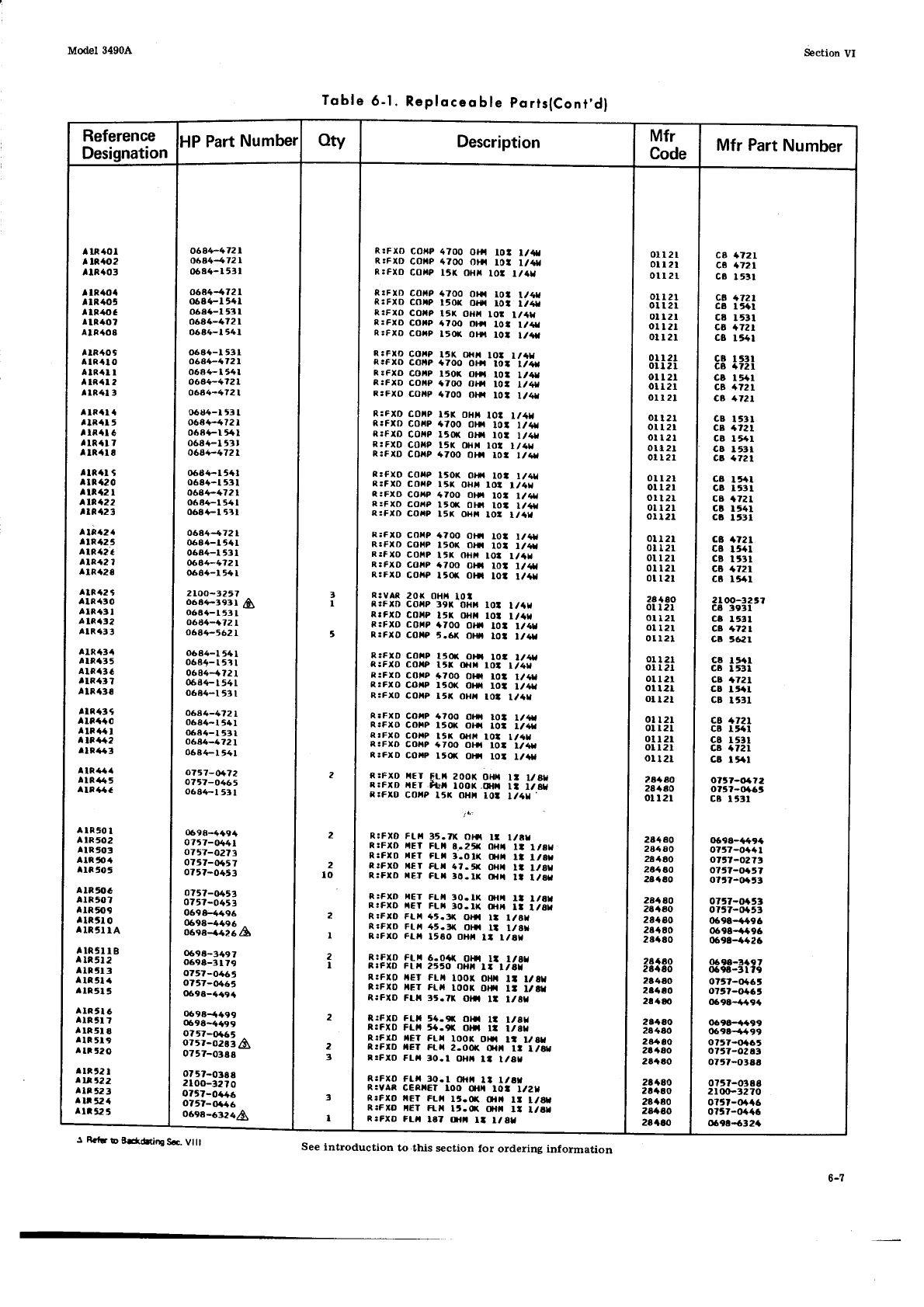
Model 3490Ä Section VI
Toble
6-1.
Reploceoble
portslCont'df
Reference
DesignationHP Part
Number oty Description Mfr
Code Mfr Part
Number
tlnaol
^üa1{J2
tlßao3
llRao{
rlrtoS
rlß4{'c
rlß/to7
alß{o8
alß409
alRal o
tlRall
!l
lRal 2
tlß41 3
tlRata
rln41 5
tlnal 6
I lRal 7
l lR4l 8
llt/u g
rtRa20
llta2 I
att,122
tt?423
at&{2a
llR425
aterei
aln{z
?
llRa28
irlR42
9
llR{30
llR4:t I
^ IR432
^lR13
!
^1R43/t
rltat5
alna3
6
It*a37
rlRt3r
llR439
/rlna{o
llt+41
a
tß44?
rlR{43
llR444
AIR.45
alntaa
a
lt50 I
a
tR 502
llR 503
ltR 50a
tlß 505
^ lR 506
AIR'O?
atR5{t9
rlRSlo
^lRSllA
rlR5llB
lll512
llt 5l 3
lln 5la
rlR 5l 5
llR 5l 6
rltSl?
^ln5l E
llt 5l 9
a
ll 520
llR52t
^tt522
lll 52
3
ru 524
lll 52
5
06s4-4721
o6a4-4721
0684-l 53 I
06444721
068t-l 541
068{-l 53 I
0684-472 I
0684-l 541
068+-l 531
o6a4-{721
0684- I 541
o6a4-4721
o6a4-4721
o6lt4-l5a t
o6a1-1?21
068{-l 54
I
o6a4-153 I
o6a1-4721
0684-1541
o68+-t 531
o6a4-1721
06a4-t 541
0684-l 51t
06a4{721
068a-l5al
o6a4-l 531
0644-4721
0686-1 541
2too-"zr7
o6i4-3e31 lil
o6a4-l 53 I
0684-472 I
0684-5621
06a4-l 54 I
o6a4- t 53
I
0684{?21
0684-l 541
0684-l 51
I
o6a4-4721
0684-l 5al
o6a4-l 5:t I
0684-1?21
06a{-l t{l
0757-0472
0757-0455
0684-l 531
0698-4+9t
o757-O{41
0757-O27:t
o75f-04'l
o?57-O453
o?5?-0453
075?-O4t3
069H496
0698-4496 ^
0698{4264
()69E-3497
0698-3179
o757-Oa65
o757-0465
069A-+{9a
0698{t99
o698{a99
o75?-0+65
ortr-ozoa l$
075?-o38S
0757-O388
2loo-32?O
o757-Oa{6
o75?-(y|46
oere-o:zt$
7
I
5
2
2
2
lo
2
I
2
I
2
2
t
a
I
R:Fxo Coftp 47oO Or|I lot t/.|a
R:FXD COI{P 47OO O}t{ lot l/{ta
R:FX0 Coäp 15(' (x{lt lot t/af
R:FID COilp 47OO O}}t rot l/{l
R:FXD COIP 15il Orfi lot t/4r
R:FXO CO,|P
l5K OH|| lot l.rtl
R:FXD Corap
+?OO Otfi lot l/4t
R:FXO COIIP
l5O( Ottl l'l ll..f
R:FXD
COftP
t5K OHta
tot lrata
R:FXO COI|P
a700 olft lot Lrfl
R:FXD COnP ISOX ol{t lO! l/4r
R:FXD COI|P
ttoo ot|t tot ttte
R:FIO Cotlp 4tO0 Olti lot l/4r
R:FXD
Colrp lsR OH,|
lot l/4tl
R:FXD COfiP aTOO Orfa tOZ tttü
R:FID COHP lt(x olil r0! 1/41
R:FXD
COxp t5t( $tt lot l/4r
R:FXD COfrP 4700 0lr| lot l/4r
R:FXO Cofap ItOK Oltt IOa l/4{
R:FXD
COilP
lt( OHl| lO: l/4r
R:FXD CO,.|P
47OO Otft tol tt,*a
R:FXD CO|P l'(X Ot|t lot l/41
R:FXD COtiP l5x ol$t lol l/tl
R:Fxo CoxP t?00 Or|t lot l/{l
RIFXD COI|P
150( olfa l0l l/41
R:FXO
COtlP
l5x oHx lot l/ar
R:FXD COXP
t700 ol|| lot l/{.
R,:FID COa{p
l'(x otft tot l/ar
R:v^R 20( OHta
lot
R:FXD
CO|IP
39K OHX lot l/tl
RtFxD COr'lP
l5X o}|x lot l.rar
R:FXD COXP
1700 0H. lot t/4r
R:FXO Cotap
5.6( O|0a lo! l/4ta
R:FXD CO,IP I50f, ol|. lot l/{r
R:F,XD
COfaP
I'f 0a{'| lO! l/4ta
R:FXD CO||P
iTOO Olfr lo! t/tl
R:FXO COXP t50( olt{ lot l/41
R:FXD
COftP
l5r oHr lo! l/aL
R:FXD COIiP 4?O0 otfi tol Ltrd
R:FXO COI|P l5(X oll l0! l/4r
R:FXO COtrP
t5t ()ttx lol t/{L
R:FXD CO||P +700 otft lot l/4r
R:FXD COXP
Itfi Orfl lot l/i|a
R:FIO tEr FLx 2oo|( ot{1 l! val
ß:FXD HEr Ftt loo(.aüfa lt l/sl
t:FxD co['|P l5x oHfi Loa tl4['
R:FXD
FLil 35.7K OHt lt l/8Y
R:FXD ||EY FLli E.2t( Ot{i lt l/sL
R:FXD xET FLt 3.Ol( lr{'t lt lrSl
R:FXD
rET FLX 6?.t( OHra
lt l/al
R:FXD rEr F[x 30-tK Ot'l lt l/sr
R:FXD rEr FLt| 3O.lK tr{l| Lt l/Et
R:FXD flET FLr 30-l.x tltft lt l/a|.
R:FIO FLr 4t.3t( Olil It l/8ll
R:FXD Ftfi 45-3t( 0tft lt l./8r
R:FXO FLt 1580 oHft lt l/al
R:FXD FLr 6.0.t' O}|| lt l/al
R:FXO
FtX ?550
oH||
lt l/81
n:FXO |.El FLt IOOI, ot{t lt l/gl
I:FIO ||ET FLt lOOr OHI lr lrar
R:FXD FL|| 3t.7( O]l| lr l/Ata
R:FID Ftt 5a-9t olt lr l/sr
n:FxD FLt| ta-9( Olil lt l/sr
R:FXD ftET FLt loof, oltt It l/sl
IIFID ||Ef Ftt 2-OO( Olli lt l/e
R:FID Ft-ft
to.l oHft lt l/ar
R:FXD
FLt 30.1 OHta
lt l/8I
R:VAI CEnl|CT loo (ltt toa lrzy
R:FXD
tET FLX lt.o( OtX lt l/AX
R:FIO llET FLX lt.(x (}tt lt l/6I
R:FID FLä la7 {}|t la lrSr
ol l2l
oll2l
oll2l
oll2l
oll2l
ol l2l
ol l2l
oll2l
o l l.2l
otl2r
oll2l
oll2r
oll2t
oll2l
oll2r
olr2l
olt2t
0lt2l
oll2l
olt2t
oll2l
0ll2t
orl2l
oll2l
oll2r
oll2r
ott2l
ol l2r
2Aaao
otl2r
oll2l
oll2l
oIL2l
01
l2t
or
l2t
oll2r
ol l2l
ol 121
oll2l
olr2l
oll2l
otl2t
oll2t
2A+aO
28{AO
olt2t
26480
28480
28480
2e460
28180
28a80
2AaAO
28480
28tEO
2At80
284AO
28480
284aO
28teo
2t4ao
2aaEo
2A{AO
2A1AO
2t180
28tEO
28r80
2rtEo
28aeo
2a480
2AtAO
2loo-t2t7
c6 3931.
ca t 53l
cB t7?l
ca 5621
cE t5al
c8 l53l
cB +t2l
cB lSal
cB l':tl
ca 1721
cB t'al
c8 r53l
ca t72l
ca l54t
o?t?-(ta?2
olt?-ot6t
c8 t53l
0698-t494
o?5?-o441
o7t7-o27,
o?5t-o+57
o?t?-ortt
0757-Or5t
ofSt-o15t
(b98-aa96
0698{a96
069a-a426
0698-at97
0698-31?9
0?5?-(16t
o?5?-0+65
069A-449{
069A-!r99
0698-+499
OltT-Ot6J
o?5?-02a3
ot5?-o3aa
0?5?-o388
2loo-32?o
o?51-oa{6
o?t7-(x46
06te-6324
cB +?21
cg 1721
c8 t53r
c8 1531
ca a?21
c8 l54l
cg 1t2l
cs a72l
cB l53l
c8 'rt2l
cB l54l
c8 l53l
c6 a72l
ca 1I2l
c8 l5+t
c8 l53l
c8 +721
cB l54l
ca lStl
ca l53l
c8 r?zl
ct lt41
ca l5tl
c8 4t2l
c8 lt4l
cB lt3l
c8 +721
cB t54t
.t Rst bB*dritESaVllt See introduction to.this sction fot ordering information
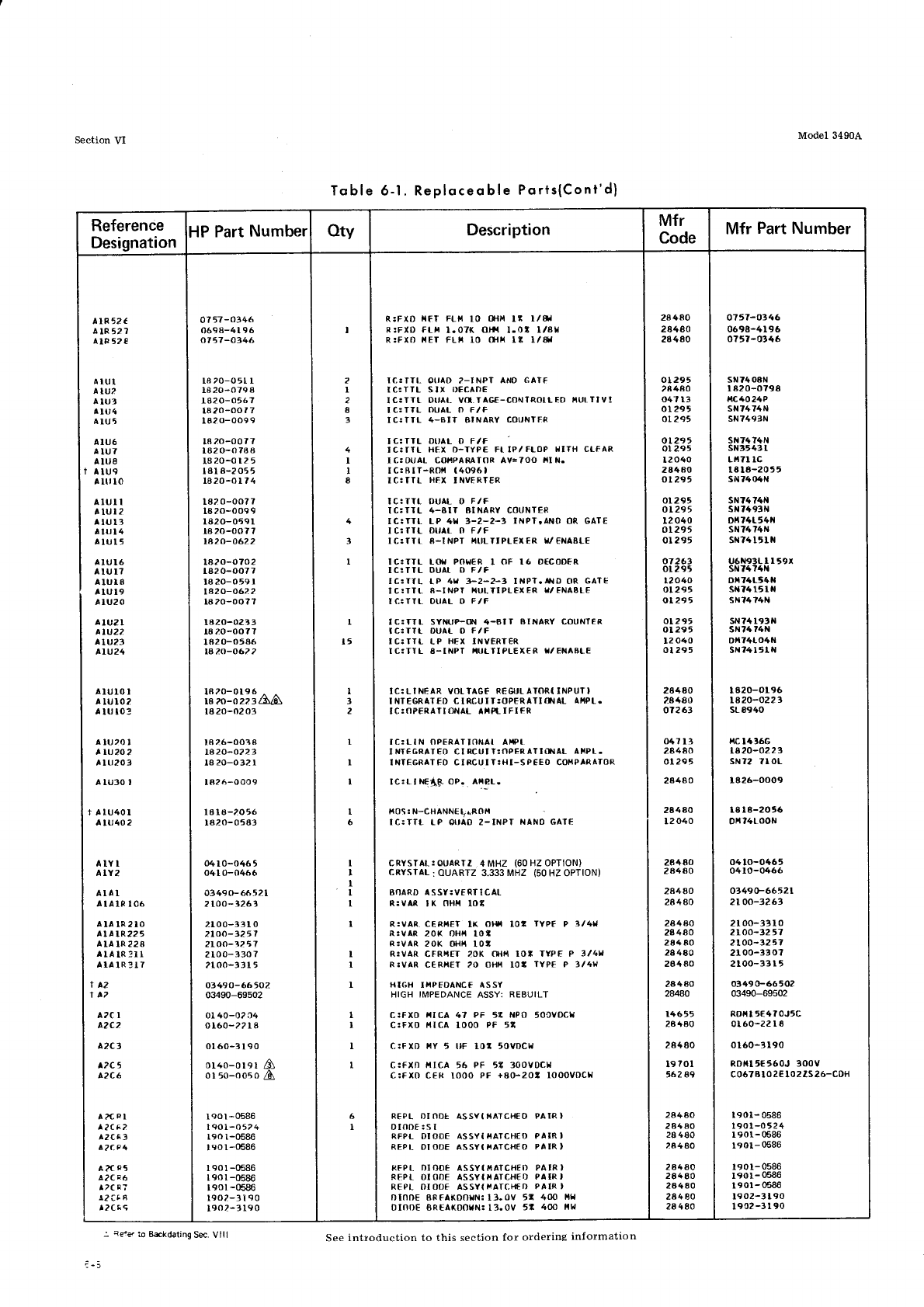
Reference
Designation
HP Part
Number oty Description Mfr
Code Mfr Part Number
lrR52{
AIR52?
alR52€
llut
A
IU2
^
lut
Ä
lu4
Ä
tu5
AIU6
A
IU?
^
lu8
^
lu9
alulo
AlUll
AIUI2
lul3
Älul4
AIUIS
AIU
I6
AIUIT
AlulS
rlu l9
Ä lu20
A
IU2I
Atu22
AIU23
^tu24
alulo I
^
lulo2
nlulo3
a
lu20 I
, tu20 2
^1U203
a lu30 t
a lu40l
^In402
AIYI
AIY2
ATAI
Ä
lalß l06
a
la lR2 lo
AIAIR?25
AIAIR228
llatRlrl
llalR3lT
1
tA2
1^?
a2c I
A2C2
A2C1
^?c5
^2C6
ar{.pl
^2CF2
^2Cr3
^2CP
1
A2CF9
^2CF6
l2cR?
12cr
a
r2c!9
0?
57-0346
0698-41
9 6
o757-O746
l8 20-o5t r
18 20-O79
8
r820-o567
1820-oot7
la2
0-oo9 9
t8
20-o0 77
182 0-o 78
8
t820-ol25
l8l8-2055
lB 20-o I 74
I 82
0-OO? ?
18 2()-O09
9
la20-059 r
l8 20-o077
ta2r)-o622
la2{)-o702
I 82 0-OO7
7
la 20-o59
l
ta20-o622
la 20-oo 77
1820-023 3
18 20-0077
I 82 0-O5 86
ta 20-062 ?
ta2o-0196
^ ^
18 ao-o 22 3
lÄ14
t8 20-02 03
l8 26-OO
3 8
ta 20-02 ? 7
18
20-o321
la26-0o09
l8l8-2056
r820-0583
04l0-046 5
04l o-0466
0349(F66521
2too-3261
2lo0-331 0
2too-a?-57
2too-az 57
2l.oo- 330 7
?loo-331 5
03490-66502
03490-69502
ol 40-02 04
or60-2218
0160-3190
or+o-orsr A
ot ro-ooso $
I eo l -0586
lcol-0524
r90 r-0586
le0 1-0586
re0l-0586
l90r-0586
t90t -0586
1902-31
90
1902-3190
I
2
I
8
I
I
a
4
3
I
I
t5
I
6
6
I
I
t
2
I
I
I
I
I
I
I
t
t
I
I
I
R:FXD }tFT FL}t IO
fl:FxD FfL l.OTK
R:FXf} I{ET FLi' IO
R:VAR CERIIET
IK O}II
R:VAR
20K OHrl l0l
R:vÄR 2OK tl}rl{ l0l
R:VAR CFRIET 20K (}tl,I
R:VnR CERIET
20 oHr{
t/&a
l/8t
l/8ta
IO' TYPE P 3/4X
IOI TYPF P 3/4Y
lot TYPF P 3/4ll
t}t|{ la
o|r{ l.ol
(I{N tt
IC:TTI. OTIAD 2-INPT AND GATF
IC:TTL SIX DECADE
lC:TTt OUAL vfl r^GE-CoNfRollED ttul.Tlv!
IC:TTL OUAL D F/F
IC:Tlt 4-aIf BINARY CoUNTFR
IC:TTL DI'AL O F/F
IC:fTL HEX D-TYPE FI.IPlFLOP IiITH CLFAR
lC:OUAL CO|{PARAIOR AV=7OO }tIN.
IC:8IT-ROtl (4096,
IC:TIL HFX INVERTER
IC:TTL OUAL D F/F
IC:TT|- 4-AIT BINARY COUNTER
IC:TTI LP 4U '-2-2-' INPT.AiIO OR GATE
IC:TTL DI,AL O F/F
IC:TTT. 8-INPT T.T,LTIPLET€R 9/€NABLE
IC:TTL LT!t{ POI{ER I OF I6 DFCODFR
IC:TTL DUAI D F/F
Ic:TfL tP 41 1-2-2-t II{PT.AO OR GATE
IC:TTL 8-INPI {UTTIPLEIER 9/FNA8L€
TC:TTI. DTIAL D F/F
TC:TTL SYM'P-ON 4-AIT 8II{ARY COUNTER
IC:TTL DUAT O F/F
IC:TTL LP HEX INVERTER
IC:TIL A-INPI'{(ILTIPLEX€R t.lENAELE
IC: LINEAR VOI.TAGF REG{,LATORI
INPUT}
I NTEGRATFD C IRCUIT:OPERATItllAL A'1PI..
IC:OPERAIIONAL IIPt IFI FR
IC:LIN OPERATIONAI AI,IPL
I MTFGRATED CI RCUI
I:NPERATICTTAL AIPL.
INIEGRÄTFO CIRCUI T:HT-SPEEO COBPARATOR
IC:LtN€1.8. OP. AxPL.
fiOS
! N-CHANNt _L
ÄRnli
IC:TTL LP OIIAD 2-INPI XANO GATE
CRYSIAI.:OUARTZ
4
MHZ (60
HZ OPTION)
CRYSTÄL:
OUARTZ
3.333
MHZ (50
HZ OPTION)
BOARD ASSY:VFRTICAL
R:VAR
IK OHH
IOT
HIGH II{PFOANCF ASSY
HIGH IMPEDANCE
ASSY:
REBUILT
c:Fxo rllca 47 PF 5r, NPO
S0CVDCId
c:Fxo rilca loo0 PF 5t
c:F xD üY 5 ttF lot SovDcrd
C:FXo IIICA 56 PF 5Z 3oOVDCH
c:Fxo cER rooo PF +8G-20! looovocH
REPL DINDT ASSY(',IATCH€O PAIR I
DINDF:SI
RFPL DIOTJE ASSYIXATCHEO PÄIRI
REPL OIODE ASSY{NATCHEO
PAIR
'
RFPL DIOOF ASSY(fiATCHED PATR I
REPL OTODE ASSYI14ATCHED
PIIRI
REPL DIOD€ ASSY(XATC.}GD PAIR '
DloD€ 8FF^KOOI{N:l3.OV 5l 400 llt
DI0DE EREA|(oOIN:13.0V 5? 40o l{l.l
28480
28480
26480
ol 295
28480
o47 13
01295
01295
ot2e5
ol 295
12040
2 8480
01295
o1295
ot295
l2 040
o1295
01295
07263
o1295
L2040
o1295
o1295
ol?95
ol 295
12
040
ol 295
28480
284AO
or263
o47 It
28480
o1295
28480
2A4AO
12040
28+80
2A4aO
2a4AO
284
80
2A4a0
28 480
28480
28480
28180
24480
28480
146 55
28480
28480
19?ol
562a9
24480
28480
28 480
28480
284 80
28480
2a4AO
24480
28480
075f-ot46
0698-4196
o?5?-0346
sN?404N
I 820-O798
t1c4024P
st{7474N
st't?493N
sil7474N
sN3543 I
Lr{71 lc
lAlA-2055
s$1740+N
sN?474N
sx7493N
Dtt7at54t{
sN?474N
sit?4 t5lli
u6N93l"
I I 59X
sN74?1il
DX7{L5{N
sl{?4151N
sN?4?41'l
sN?4 l9:!N
sN74?4N
Dlt74l-o4N
sN?4 I5l l{
I 820-O196
ta20-0224
sLg940
ltc 14t66
LA20-O221
SN7?
TIOL
I 826-0OO9
l8 l8-2056
0x74LOON
04lo-o{65
o4lo-0466
03490-665 2l
2too-126?
2loo-3310
2too-1257
2too-1257
2l o0-33 0?
2 loo-33 I 5
0349 $-66502
03490-69502
ROr,ll5E4?0J5C
0l 60-22 I 6
o 160-3190
RDfaltES60J 300v
c067
Bl0 2E
102 zs26-cDH
l90l- 0586
I 901-o 5 24
I 901- 0586
leol- 0586
1901-
0586
l90l- 0586
l90l-0586
l9
02-3
I
90
1902-3
t 90
Model 34904
Section VI
Toble
6-1.
Reploceoble
Ports(Cont'd)
qers'@ Sekdating Ss. Vlll See introduction to this section for ordering information
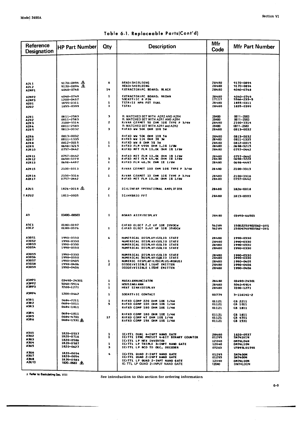
Reference
DesignationHP
Part
Number oty Description Mfr
Code Mfr Part
Number
A2LI
^2t2
l2xPl
^zl|P2
Az'|P3
^201
^202
A2n I
A2t2
l?R3
t2F{
A2R 5
12R6
^247
l2R I
^2ß9
l2R lo
l2t ll
^21R12
lzR r3
t2R 15
l2n l6
A2nl?.
AArl
t ^2u2
l3
l3cl
Atc2
l3DSl
ltDs2
130s3
t3D54
130s5
l3D36
130s7
l30sa
130s9
I3TPI
^?,,'P2
t:ttp3
a3lrP4
^3Ul
l3lr2
lar3
l3{ra
l:Ir5
l3tJ6
l:lt ?
rta
A3J!O
t3R
t
r3n2
l3R3
r:!Ra
t3t5
atn6
9l 70-0894
9l 70-0894
40,40-o748
4040-0749
t200-o437
l8 t5-o:|l I
lat5-o399
oE
I l-2583
08 I l-258 3
2too-ltr4
08 ll-258:l
08
l3-oof2
oal 3-oo32
oSll-1335
08 l2-oor 5
o69a-321 5
Ol'l-Ot 42
0757-0442
069A-t?7 A
069a-4497
2 loo-331
3
2 loo-33t 6
0757-O..42
lE26-OOl I
l8l3-ooo3
03/t9G-665G1
ol 80-ol 97
ol.8(F0376
1990-o33
0
199(FO330
1990-o330
199(FO330
1990-o330
t99(FO330
199(F0405
199(FO{06
199(FO406
o349(F24301
5040-591.4
72o(Fl27l
1200-o452
06a+-221 I
o6a4-lol I
o68a-l 8l I
068Fl8l I
o6a{{701
oaa+-rrtt
$
la z(FO53 7
1820-o?16
la2(FO5A6
Itz(FO5A7
ta2G{62?
t820-oo5a
182(HO5a
16z'(H583
reeo-sg A
A
A6
l{
I
I
I
I
I
3
I
2
I
2
I
I
I
6
3
2
a
l?
I
2
I
I
I
I
I
t
I
I
I
t
{
AOARD ASSY:OI SPLAY
afAo: sn I EL Dlt{G
BEAD:
SHI EIDI '{G
EITRACTOR:PC 8OARO. Stlcf
EXTRACTOR:PC.
8OAIO. Bß,Ott
SOCKET:IC
I Pl}|
TSTR:SI ilPN FET DIAI.
ISTR3
R: MATCHED SETWITH
A2R2 AND A2R4
R: MATCHED
SET WITH A2RI AND
A2R4
R:YAR CERXET 'O OI.'| lOI IYPE ? 'I4I
R: MATCHED
SET WITH AzR' and A2R2
R:FXD IU 50X (I.ilt lot 5r
R:FXO tl 5o|( tl{t lo! 5l
R:FID tt llt( (}tx 31 3l
R:FXD yr I OHfr
3t 3r
R:FXO FLlr 499( OHX l.ot l/0a
R:FXD XCT
FLX IO.OX artil ll lrBX
R:FXO tEI FLft 10.(X t,lra ll l/8r
i:FXD ||€l FLlt 49.9( Ol{X
lt l/8t
R8FXD FLr{
46-7K Otil lt l/tL
R:VAR CERI'ET
IOO OHil IO! IYPE P 3/4Y
R:VAR CERrf€T
lO Olfi lot lYPe ? tt4y
f,:FXD rET FLt| lO.O( (t{H lt l/8t
IC:I.INEAR NP€RATI(r{AL AI{PITF IER
IC:HYBRIO FFT
C:FXD
ELECT 2.2 UF IOt
c:FrD ELECT O-a? tt lot
NI"ERTCAL OISPLAY:SOLID
SIATF
iauHERtcAt-
Dt sptAv 3solt D srAT E
NUIERICAL OISFT^Y
:SO|_IO StArE
NUI{FRICAL
DISPLAY:SOLIO
STATE
NI,{€R,TCAL
.DISPt
AY:SOLID STATE
NU||ERICAI DIS9LAY:SftrlD SrlrE
ilt l€R.lC OISPL|IY
:t€OI PLUS-fi
tlUSl
DIODE:VISIATE
LI6H' EXITTER
DIODE:VISISLE
LIEHT
EIII'ER
tilsx: INNUNCt Atan
H(ruS IilG: liltl
HEAT SI TT:DISPL.AY
SOCXET! IC COI{TACT
R:FXD COI|P 220 oHil lot l/ar
R:FXD COXP LOO
(}rt lol l/41
R:FIO COrtP 180 oHra
tot r/al
R:FXD COftP 180 (}{t tol l/4Y
tIFID CO||P
47 oHt lot l/tr
R,IFXD Coftp I't (}t,l lot l/ar
IC:TTL DUIL .-IilPT TAI{O GATE
ICaTlt- SVIC PRES€T
4-ttl Btl|lny OOtttTER
IC:TTL LP I.IEI I}IYERTER
lclrfl LP TRIPLE '-Itfr it||t 6lTE
lCtTlL LP 0CD TO IEC- DECOIEI
ICsff|. OUAD 2-It{Pl llAl'lD
Gll€
lc:rll otnD z-lflPt ilrxD GllE
lc:Yrl LP QIJAD 2-l|{Pr illilO 6^lE
lC:TTL LP OUAD
2-INPUT NAND
GATE
20vtf,ll
35UlCra
28+00
28480
2A{80
28t80
l7l l?
28tAO
28480
2W
28480
2Aa80
28480
28180
28rEO
28480
2E480
2A48(t
2A+80
2a+60
24t80
28aro
28+OO
28t80
28t80
28480
2aaro
284€O
562a9
*2e9
28480
28460
2a460
2AaAO
28a80
2a460
2Ateo
28+80
284AO
48a80
24460
28aAO
oo?79
oll2l
oll2l
olt2t
orl2l
ol t21
ol t2t
2A4AO
ol29t
12040
l20ao
ofz6t
o1295
ol29t
l20ao
12040
9170-o89a
9l 70-o89a
tO{)-{1740
40{o-o?r9
5r66-2t5-t
I A5t-O3l I
lESt-ot99
G11-258it
611-2583
2 lo0-3tl +
(Blr-25€B
08l1-oo32
081:l-o032
osll:l 33t
08t2{ol5
,069e-32rt
ofSl-oa{z
0757-o.}12
069e-122r
0698{t9?
2l(xF33rt
2l o(F3316
0757-O+{2
la26-oola
la l3-ooo3
o:t4.9{F6650t
r5|n225I902012!OVS
ItOD'fl+I9O3512-OYS
199(FO3lO
199(Ht330
l99H3tO
199(H3tO
1990{t330
1990-o3to
ltxr(H).o'
l99tH)406
tr9Hto6
0369(F2+301
'{)4H91a
7200-127t
:Fll614l-2
22tl
I 0tl
Irl I
l8l I
t70l
lStl
1820-or37
sxll15lil
dr?+L('+r|
Dft?4Llot
('rt93LOl59X
sl|?a00r{
slt?aoor
Dr?tLootl
DMT4LOON
c8
ca
c8
c8
CB
c8
Model 34904 Section VI
Toble 6-1. Reploceoble
PqrtslCont'dl
See introduction to this ection for ordering information
.1 Rdrb Büd.tiESa Vill
6-9
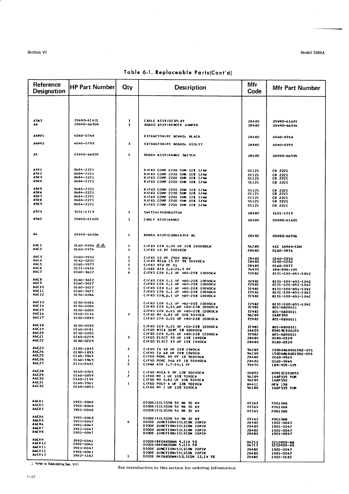
Section VI Model 3490A
Toble
6-1. Reploceoble
Ports(Cont'dI
Reference
Designation
HP Part
Number oty Description Mfr
Code Mfr Part Number
a3t3
^4
a4t{Pl
a4t4P2
^5
ASRI
^5e2
A5R
3
a5ß4
A5R5
/r5ß6
r5ß7
5R 8
l5ß 9
a5s4
^sli2
A6
a6c I
^6C2
a6c3
^6C4
A6C5
a6c6
^6C7
a6c8
6C9
r6clo
6Cll
A6Ct2
l6cl3
l6c 14
^6C15
^6C t6
l6c l7
l6c la
l6c l9
r6c20
Ä6C21
^8,2.2
A6C2?
46C24
A6C25
46c26
^6C27
a6c?a
16c29
A6C!iO
l6c3 r
^6C12
A6CR
I
l6cR 2
A6CR
3
A6C94
l6cR5
A6CR5
16c87
A4FA
^6CR9
t6cP I C
racP I I
L4.Rt2
r6€e I !
0349O-61 6r)l
o3490-66 504
4040-o748
4040-0755
03490-66505
o6a4-2221
o6a4-7?,2
|
o6a4-222L
o6a4-2221
06a4-22_21
06a4-222_l
o6a4-2221
o6a4-2 22 |
06a4-2221
3rol-1719
03490-61 605
03490-66 506
orso-oeo+ $$
ot 60-3976
o I 60-3930
oI 40-o202
o
I
60-:r977
ol 2 I
-o436
ol6()-3622
ot60-36?2
oL60=1622
oL60-3622
oL60-3622
0l 50-ooa4
ol 50{) oa4
ol 50-o093
ol50-o093
ot
60-2
134
o
I 50-o093
ot 50-o093
ol60-0lal
ol 50-o093
ol 60-o22
9
ot 80-022 9
ol 80-
I
835
ol ao-l 83
5
o
I
60-394 5
0l 60-3 91 9
o I 2
t-0432
ot 60-o763
ol 60-oa59
ol60-2114
o160-3501
ol 60-oa5 9
I
90
l-oo{o
190 l-o040
190
t-0040
t
90l -oo40
190
t-oo47
I90 l-o047
190
l-oo47
I
90
l-oo47
1902-OO4l
1902-O04l
190
I{)O47
I 901-o047
190
2-3
la
2
t
I
3
I
I
I
I
I
6
2
t
2
t
I
?
I
?
I
6
I
CAALE
ASSY:OISPLAY
AOARO ASSY:REHOTE
JUXPER
EXTRACT0R:pC
ao^Ro. Bt-aCK
EXTRACTOR:PC
8aAR,D.
vIoI.FI
ßOARD ASSY:RAIG€
Sr|ITCH
R:FXD COilP
2200 oHr{ lot l/41
R:FXD COf'rP
2200 r}Jr4 lot l/4r,
R:FXD COXP
2200 oHti lot l/{r
R:FXD COtiP
22.OO
Otl4 tor, tll.U
R:FXD COHP
2200 0|x4 10t l./4ll
R:FXO COHP
2200 0ttt toa l/{r
R:FXD COI{P
2200 O|{1 lll tlg
R:FXD COtlP 2200 (l}}t lot l/41
R;FXD
CONP
2200 Or+{
tot l/4ta
SII TCh: PUSHBUIION
CABLF
ASSY:RANGF
BOARO ASSY:CONYERTFR
c:FxD cER O.O5 ttF 20t lOOoYDcta
C:FXD
lO PF 5OOVOC|a
C:FXD
lO PF 25OO
yocta
C:FXD XICA
15 pF Sa 5oOVDCI
c:FxD 970 pF Ol
c:vAR AtR 2.1-24.5 PF
c:FxD cER O-l rrF +ao-20t loovocl
C:FXD
CER
0.t trF +ao-20t loovocr
c:FxD C€R O.l UF +8O-2O! IOOVOCX
C:FXD
C.ER
O-l UF +8O-2Ot lOOyDCta
C:FXD
CER O.l UF i80-20: loovocl,
c:FxD cEB^p.l uF +8o-2oa loovocl
clFxD CER O-l UF +ao-201 lOOvDCr,
c:FxD cER O.Ol;tF +80-201 loovocH
C:FXD
CER O.0l UF +ao-zot loovDcta
c:FID HY O-a2 UF lot 5ovDctl
c:Fxo cFR o-ot uF +ao-z0t loovDcl
c:FXO CER O.Ol UF ia0-201 loovDcr.
c:Fxo nIcA 30PF 5t 300vDct
c:FxD cER O.Ol UF +8(F20t IOOVDCT
c:Fxo €L€cT 33 UF lot tovoo.
c:flo EL€CI 33 UF lot lovocl
C:FXD
TA 6A UF 2Ot l5yDcy
C:FXD
TA 6A UF 20t l5YOCr
C:FXD pORC
39 PF lt 500vDc|.
c:Fxo PoRc
346 PF lt 500vocy
c:vAR ^tR 1.7-14-l PF
c:Fxo ItcA 5 PF lot 500vocr
c:FxD rY I UF lol 5oVDCy
c:FxD t1Y
O.82 UF lot 5ovDcr
c:FxD PO|-Y
4 UF lot 5oYOCt.
c:FxD tY 1 UF lO:'oVOC|
OIoOE:SItICOil 50 IJI 30 tav
DIOO€:SILICON
tO |t^ 30 rY
DIOD€:Sll-ICOt{
5O ftA tO ry
olooE:sn tcoia 50 ta 30 rv
DlooE JUr€tIoN:StLICtt{ 20PrY
DIOD€
Jul€TIoN:Slt-IC0ta 2OptV
DIODE
JUlrlcTl Ot{:S
It-Ic(rl 2Oprv
oIooE JUNCTITil:SiLIC(X 20PtV
olooE:aR€aKootaN
S.llv 5t
DIOOE:BREAKDOTI{
5.IlV 53
DIODE
JUifTIOil:SILIC{}I zOPIV
DIOOE
JUI{,IIO|{:StLIC{I{ 2OPIV
Dloo€ 8RE XDOYit:SILICON
12.tV 5:
2a4AO
28480
2A4AO
24480
28480
orr2t
01121
oll?l
olr2l
ol l2l
ol
l2l
oll2l
oll2l
otl21
28460
2A480
284 80
562 69
2A4AO
24480
2 A480
28480
74970
729a2
t2942
72982
729a2
729A2
729A2
729A2
72942
729A2
*2A9
f2982
129a2
14655
72942
24480
28+80
'6269
562 A9
28480
28480
74970
00853
56249
562 A9
844I1
56289
07?6t
0726t
07 263
o7263
28 480
28480
28480
2a+80
o{713
0471,
2r480
2Et80
28480
03{90-6 l60l
03490-66504
404{FO74a
4040-o755
03490-66505
222L
2221
222L
222!
2221
2221
2221
2221
222L
CB
c8
c6
ca
ca
ca
ca
c8
ca
Slot-17 l9
0349(F61605
03490-66506
{lc t69t4{oH
ol60-39?6
ol60-3930
0140{!202
olöo-3977
l89_t09-l05
81 3l-l O0-65
l-l 04Z
8l:rl -loo-651-l o{z
8l 3l -I OO-65
l-l O4Z
6 I 31.-tOO-651-l Otl
8l 3l -l 00-65 l-r 04z
rl 3l-loo-65 l-l o4z
8l:tl -l 00-651-l oaz
801-K8000 I I
801-K8000 ll
la8Pt50
rol-K8000 r
I
tol-|(aooo I t
ROItl t€tooJts
aol-xa000 ll
ol80-0229
ol60{t229
1500 6&tIo0ttn2-oYs
l5006E6IOOl 5R2-DYS
ol50-3945
ol60-39a9
189-505-l Ot
RDHI
5CO50K5S
!.48P335 Ptrl
l4aP350
H€t 138
t+4P335 Prtl
FDGI
08A
FDGIOSs
F06t 088
FDGI08A
t90l-oo47
l90l-004?
1901-00t7
t90l-004?
szl o939-98
sz 1o939-98
l90l*ooa?
l90l-0047
L902-tta2
: geier b BddatirE Se. Vlll See introduction to this section for ordering information
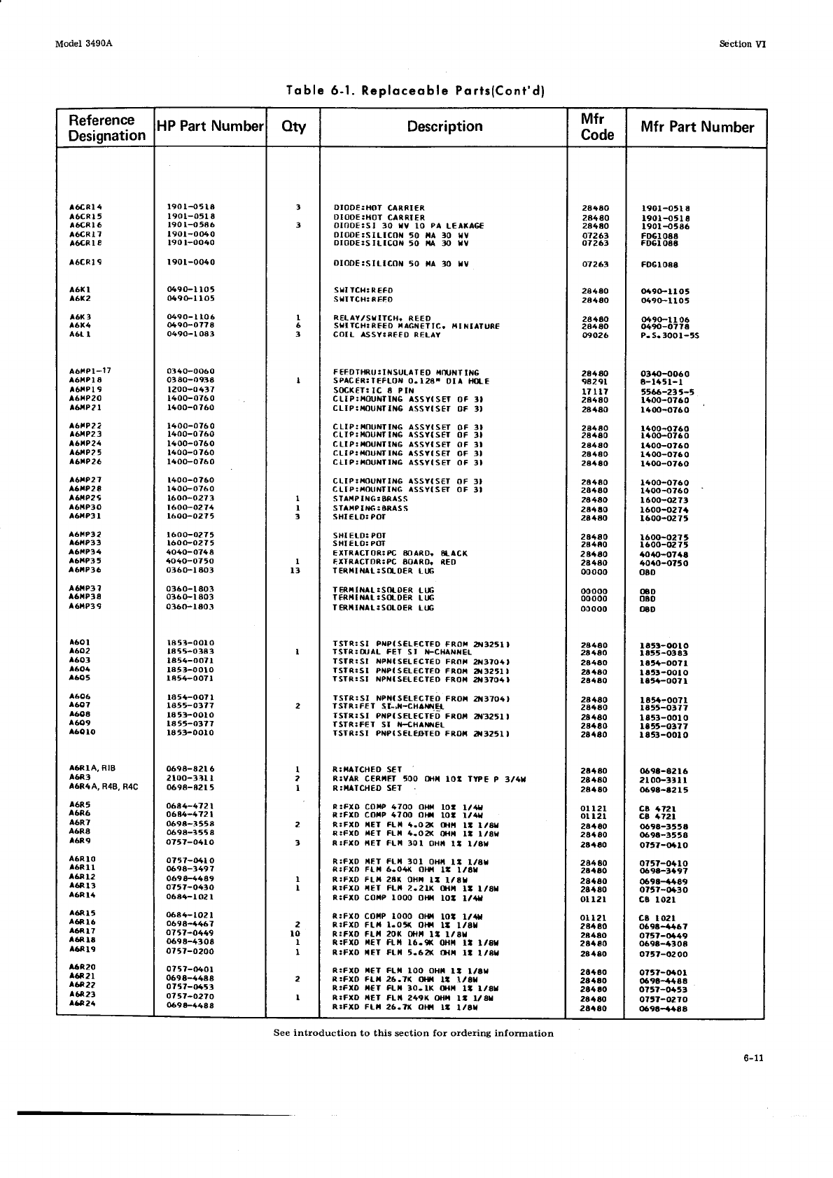
Model 3490.A Section VI
Toble
6-1. Reploceoble Ports(Cont'df
Reference
Designation
HP Part Number oty Description Mfr
Code Mfr Part Number
l6c Rl 4
a6cR I
5
l6cRl 6
a6cRl 7
a6cR
I 8
6CRl9
a6( I
a6(.2
l6t( l
t6t(4
a6t I
A6t
Pl-17
A6XPI I
A6r{Pl
9
^6AP20
t6tP2 I
^6tP22
^6AP2t
^6tP24
6AP?'
A6't?26
^6AP27
a6taP28
a6nP29
A6t4P30
a6rP3 I
a6)4Pt2
l6t{P33
ll6tP34
A6taP3 5
l6rP36
A6f,tP3 ?
l6f{P38
A6riP3
9
1606
4607
160E
4609
A6Q
IO
A6RIA, RIB
A6R3
A6R{4, R4B. R4C
A6R
IO
r6Rll
l6n l2
l6R 13
A6R
14
l6Rl5
a6ß
l6
A6R
l7
A6t ta
l6e 19
46e20
A6n2l
^6n22
46e23
^6e 2a
460
I
^602
r603
^604
1605
A6R5
Ä6n6
A6R7
A6RA
A6R9
190 I
-o5
ta
l90I*o5l 8
190
l-o586
l90l-o040
t90 l-oo40
I
901
-0040
0490-l I o5
o{9(Fl I 05
o490-l lo6
049(FO?78
0490-l 083
0340-oo60
03ao-o93a
1200-o437
1400-o760
1400-o?60
1400-076 0
1400-0760
1400-o760
1400-0760
l{oo-o760
t400-o760
1400-o760
1600-o273
t600-0274
1600-o275
I 600-o27 5
1.60{F0275
4040-o748
4040-0750
o360-l ao3
o360-t 803
036(F1803
o36{Flao3
18 53-OOl O
l8 55-O38
3
la54-o07r
la53-o ot o
I 454-O07l
la5+-oo7 I
la55-o177
185:FOOIO
l8 5t-0377
185:FOOIO
0598-821 6
2too-331
I
0698-82 I 5
0684-472 I
0684-4?2 I
069a-355a
069A-355 A
o75?-O4lO
0757-04t O
0698-3497
069H489
0757-O430
o6a4-l 02
I
o6a4-l02 I
069a{467
o7t7-0{69
0698-4308
o?57-O200
o7 5?-0401
069A-a488
0757-(x5a
075f-o270
069H488
1
3
I
6
3
I
I
I
,
I
I
I
I
l3
2
I
?
I
2
3
2
lo
I
I
2
I
DIODE:HITT CARRI€R
DIOOE:HOT CARF,IER
DIODE:SI 3O t.V IO PA L€A(A6€
DIoDC:SlLlCOt{ 50 ,aA 30 HV
DIODE:SILICON 50 'IA :x) t.V
DIODE:SI|-ICON 50 f{A 30 tV
SHI TCH: R
EFD
S II TCH: R
EED
REI.AYlSUITCH. REED
STTTCH3RFED
TAGN€TIC. IlTNIATURC
COIL ASSY:R€FD RELAY
F
EFDIHRI' : IIISULAI ED IIfl'NT IN6
SPAC€R:IEFLON O.l28r DIA lt(I-E
SOCK€T:IC 8 PTN
CLI P:I4OUNTIXG ASSY(
SE
CLIP:I{OUNITNG ASSYI
SEf
C
LIP: IIOUNTING ASSYI
SET
CLIP: llOUNf
lilG ASSY(SEr
CLT P: IIOUNTING ASSYI
SET
CLIP!I{OUNTING ASSVI SEI
CLI P:FOUNTIilG ASSYI SEI
CLIP;I,IOUNTIilG ASSYI
SET
C,LT P!XOUNTING ASSYI SET
s TA|{P
I XG:8tÄSS
STATP I 'IG: BRAS S
SHI EI-D: POf
SHI ELD: POT
SHI
ELO: Pof
oF lt
oF 3t
oF 3l
oF 3l
oF 3l
oF 3t
oF 3l
oF 3l
oF 3l
EXTP,ACTOR:PC BOARD, 8f ACK
EXTRACTOR:PC SOAROi RED
IER'iINAL:Sü.D€R LLß
f ERII IN f ! SOI-DER
IERI.tI NAL:S(LOER
I fRII INAL: SOTOER
LI,,I;
Lrß
LI.G
TSTR:SI PNPISELECTFO FROT' ä{32'II
rSTR:ü,AL FET SI N-CHANNEL
TSfR:Sl NP|ISEIECT€D FRot at3to4,
lslRrsl pltP(sELEcTEo FROX ä{32511
TSTR:SI NPiIISELECTED FRO'I A'3?O4I
TSTR:SI lpn(S:t-tcrtir FRox 2it37041
TSTR: F€T SI.J{{HA'ü.T
ISTR:Sl pNpISELECTFD FRO|4 atf2ilt
f SIR:FET SI IIH,HAN''IEL
TSTR.:SI PNPISELEOTED FROII AI32'I I
R:IIATCHEO
SET
R:VAR CERr;r 500 rlOt lot TtpF p 3/4ta
R:IIATCHEO SET
t:Fxo coltP 4700 0l0t 10: l/4L
R:FXD CO|1P 4?OO Otft 101 l/41
R:FXD ltEr FLil {.oa( (}tft lt l/8r
R:FXD |.€t FLft +-Oa( üilt l: l/8t
R:FXO flET FLll 301 OHft
tt l/8L
R:FXD ilET FLft 301 OHfi l! l/81
R:FXD FLil 6.04r( OlTl lt l/8I
R:FXD
FLlr 2A( OHfi
t: l/81
l3FxD [|{El FLn 2-.21K (I{}t l: l/8ta
R:FID COrlP IOOO OIH lot l/afl
R:FXO COI|P IOOO Otet lot l/4ta
R:FXD
FLra l.Ot( Ottt tZ ttAY
R:FXD FL'I 2OT OHT
II I/8I
R:FXO frET FL'| 16.9( OHil l: l/8tl
R:FXO tET FLil 5.62( (l{'| lt t/al
R:FXO n€T Ft
f{ lO0 oHft tt l/al
R:FXD FLta 26.7( 0{t tt 1/8r
R:FID il€r FL|. 30-lK O{tt ll l/Ar
R:FXD tEl FLl| 249K Otft l: l/8r
R:FXD FLt 26-?( Olft l: l/al
24480
2A4AO
28440
o7261
0726!
o7263
2844O
28480
28480
284EO
09026
2A+AO
2A4A0
264AO
2a480
28480
2AlAO
98291
lTll?
28480
2814O
28480
28a80
2A4aO
28460
28{AO
28480
2A4AO
28a60
28480
ooooo
ooooo
ooooo
o0000
2A4AO
28+80
2A480
2a4AO
2A4aO
28480
28480
28{aO
2a180
24180
26+AO
28+80
28a80
orl2l
ol l2l
2A+80
28480
24480
24480
28{80
2aa80
28{80
ol 121
orl?l
28480
2a480
28r80
28{SO
28t80
28aao
284EO
2Aa80
2aaao
l90l-o5l e
l90l-o5t I
l90l-o5a6
FDGIOAS
FD€I
088
FOGtOaS
o+9(Fllo5
0490-tlo5
049(Fl I 06
0490-o778
P- S. 3001-55
03ao-oo60
a-1451-t
5566-2tJ-5
1400-o750
l4O0-O76O
l4OO-Of6O
lao(H)760
t400-o760
1400-ot60
1400-o760
I400-o750
1400-o760
1600-02t3
1600-o27{
1600-02?t
1600-02?t
1600-0,27t
toao-o?4a
40'rO-O?5O
OBD
(nD
oio
oaD
la53-oolo
la55-o3a3
l65t-oo7l
lA53-OOIO
laSt-oo?t
l85a:oo7r
r85t-o377
1853-OOtO
1055-03?7
r 853-OOl
O
0698-8216
2loo-3rl t
0698-a2 I 5
cr r?21
cB a72l
(1698-3554
0690-3558
o?5r-orlo
0757-OrlO
0694-3497
069A-++a9
otrT-|J4ao
cB lozt
cE lo2l
0690-*467
o?57-Ot49
0698-4308
075?-O2
00
o?5t-(rol
0690{488
o?57-Oa53
o79l-o270
o69t{48A
See introduction to this section for ordering information
6-11
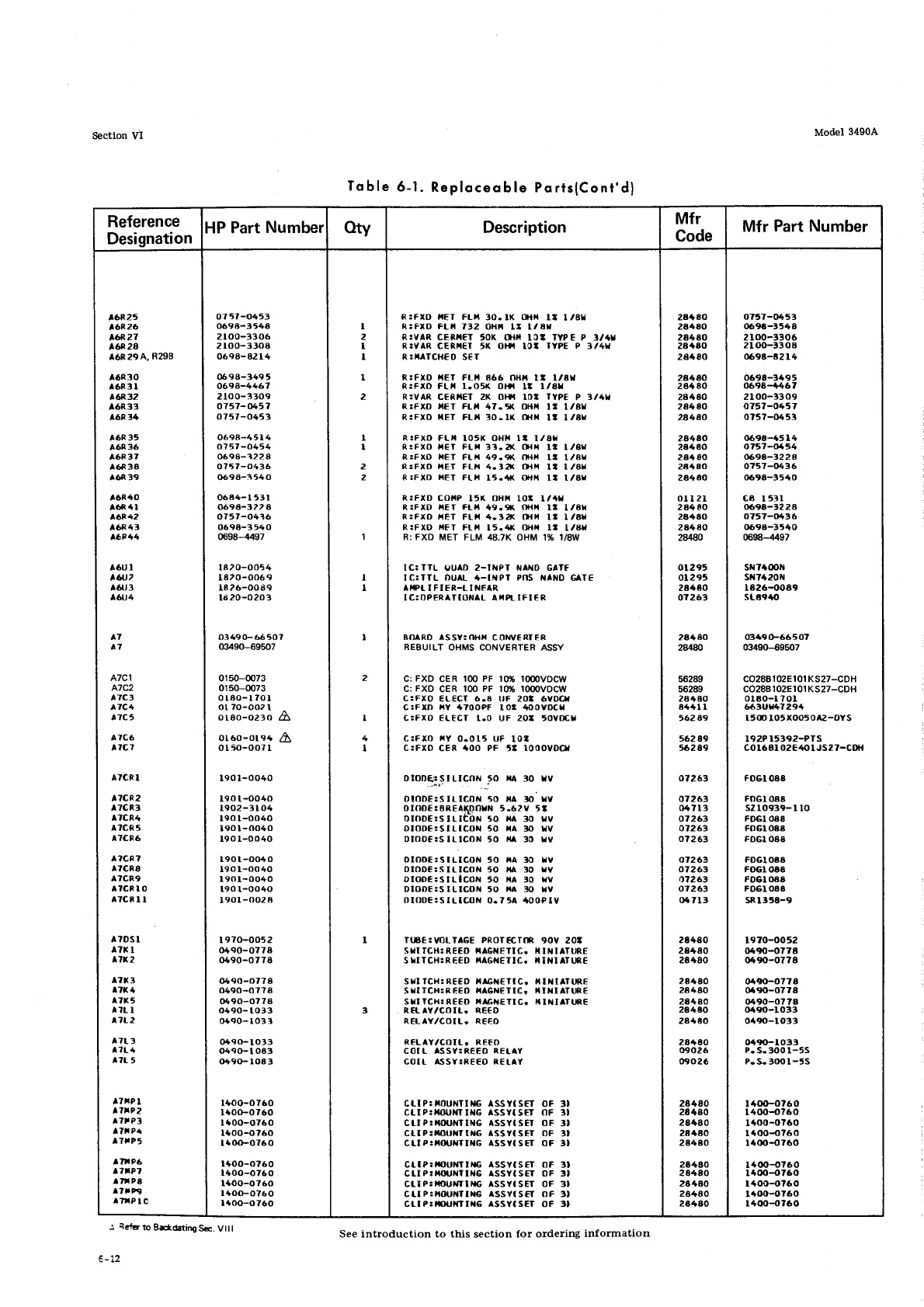
Section VI Model 34904
Toble
6-1.
Reploceoble
PortslCont'dl
Reference
Designation
HP Part
Number otv Description Mfr
Code Mfr Part
Number
A7
A7
^6R?-t
t6R26
A6R27
a6ß28
A6R29A,
R298
A6R3O
A6R3 I
A6R32
46R33
A6ß:t4
t6n 35
a6ß36
A6R37
16ß 38
A6n 39
l6R{O
A6R4l
46342
46n43
^6944
A6U I
^6tt2
461,3
A6TJ4
ATCr
A7C2
A7C3
a7c4
^7CJ
l?c6
^1C7
ATCRI
^7Ce2
l7cR3
A7CR4
A?CR
5
Ä7CR6
A?CR7
l7cR8
^7CR9
A?Cn I O
aTcR I I
A TDSI
A7X
I
^7X2
l7t3
l7t4
l?r5
t?L I
^7L2
A7t 3
/l?L4
l?L 5
l?xP
I
^7r92
^71P3
l?t P.
l7rP5
ltrP6
ttaPT
t1i|'? t
l7rP9
rTxP I C
o7 57-0453
069a-3544
2loo-3306
2
loo-330a
0698- 821 4
069a-349 5
069A-4467
2lo o-3309
0757-M57
0751-O45t
0698-45 I 4
0757-O454
0698-122 I
0757-O4a6
059a-3540
0684- I 53 I
o59A-322 A
o757-0436
069a-3trO
0698-4497
1820-O054
1820-o06 9
t8
26-00a9
ld 20-o20 3
0349(F65507
03490-69507
0150-@73
0150-0073
0[ao-1701
ol 70-oo2 I
o 180-o2 3 0
ol
60-ol 94
o I 50-o07 I
190 l-oo40
190 t-oo4()
1902-3 I
04
190 l-0040
t90l-oo40
190 l-0040
t90 t-o04 0
190 l-oo40
l9()l-0040
190
t-o040
l90l -o02
a
197(FO05 2
0490-0774
0690-o778
0490-o778
o490-o77A
(x90-077a
0490- t o33
0490-1033
049(FlO13
(}49(Fl Oa3
o+9(F lo83
t40(Fo760
lao(F0760
l{o(Fo760
l{oo{?60
t+oo-0760
It{)0-o?60
140()-o760
1400{760
l{o(Fo?60
laoo-o760
A
A
I
2
I
I
I
2
I
I
2
2
I
I
2
I
I
I
I
I
3
R:FXO arET FL|t 30.IK oHX l: l/81
R:FXO FLf{ 732 oH}l tt l/8L
R:VAR CERH€T 'OK (It}t IOI TYPE P 1/4I
R:YAR
CERiET 5K O|ä lot lf?t P 3t4r
R:!1ATCHED S€T
R:FXD ftEl Ft-H 866 oHn lt l/a||
R:FXD FLX l.O5{ O}rI lt l/8I
R:VAR CERI,IET 2K OTTI IOI TYPE P 3I4I
R:FXD XET Ft-t{ 47-5r( OHtl lt 1/8I
R:FXO
l|ET FLil 30-lK o.tx lt l/8r.
R:FXD
FLX lO5( OHX la l/8r
R:FXO |(€T FLx 31.a( tH|| lt I/8U
R:FXD t(ET FLll 49.9t( ottx l: l/Al
R:FXD tfET Fa-A 4.tX, (}lt{ It l/6L
R:FXD fiET FLtl 15.4( (}ilt lt l/ar
R:FXD COilP
l5K OHt{ lot l/+t
R:FXD rlET FL|| t9.9( ()+0{ ll l/8r
R:FXO tET FLI{ 4-1ä( at{H lt lrAU
R:FXO f'lFT FLr{ t5.4r( ()|rX ll t/8r
R: FXD MET FLM /t8.7K
OHM 1% 1/8W
TC:TTL gUAD
2.TTPT NAND GATF
lC;TrL DUAL 4-INPT PnS f{ll{O GtT€
IIPLIFT€R-LINFAR
IC:OPERATTONAI ATPL TFI€R
BO RD ASSY:OHI{
COWER'ER
REBUILT
OHMS CONVERTER
ASSY
Cr FXD CER 10O PF l0% lomVDCW
C:
FXD CER 10O PF 1096 loooVDCW
c:Fxo EL€CT 6.6 UF 20t 6YOCJa
csFID nY 4700PF lOt 400YDCI
CiFXD E|.€Cf l.O UF 2Ot SOVOCI
C:FXD,rY O.Ot5 UF
lol
c:Fxo cER {oo PF 5t r000vDoa
DIODg:SlLlCnN 50 r|A
1O lV
.-l
OI0DE:StLtCON 50 XA 30 l{Y
oIoDE:EREAlpOrN S-62Y 5t
DIODE:SlLICOil 50 ilA 30 t|v
DtoDE:SILICON 50 ft^ 30 |lV
DIOO€:S|LICON 50 r 3C rV
OIOD€:SILICON 50 llA :10 lY
DIOO€:SILICOiT 50 ltA 30 rV
DrooE:sILlcoN io ria 30 rv
DIODE:S lLtCOt{ 50 ra 30 t{Y
oloD€:sILlcoN 0.75a tooPIv
TTßE:VOLTACE PROTECT(N 9OY 2OI
STITCH: REED t|AellETIC! lllt{lATt RE
S IITCH: R
€€D I'AGI{ETIC. }tI NI TTJRE
srI rcH: REED lttßr{€Ttci nlr{tATURE
SHITCH:RE€O IIAGN€TTCi IIINIATTNE
STI TCH: REEO IIAßIiETIC. II
II{IATINE
RETAY/COIL. REEO
T,ELIY/COTL, REEO
RFLAY/COIL. REEO
COIL ASSY:REEO R.EL Y
COIL ÄSSV:REED RELAY
CLI P: IOUilTIilG ASSYI SFT
CLIP:|{I,TT ING ASSYI
S€T
CLI P:
||OUXTTilG
ASSVI
SEI
Cl-IP:toul{ttt{G ASSY(SEr
CLI P:iq,XTIilG ASSYI SET
ct_lP: illut{TlL6 AssY( sEf
cLlP:xot xllttc AssYl sEI
ctt P:
r{ou|,rlrG AssYt sEI
cLt P:tot if tr{G lssvt s€I
c|-lpstt)t Ntlxc AssYls€T
oF 3t
oF fl
oF 3l
oF 3l
oF 3l
oF 3t
oF tl
oF 3l
oF :D
oF 3l
2a+80
28480
2A480
28aao
2A480
28440
28t80
2A4aO
28480
28{80
2A4AO
28680
28480
2a+80
2a400
oll2l
284 80
2844O
28480
28480
ol 295
ot295
28+80
07 263
24480
28480
56289
56289
24480
84+l I
5628e
562
89
56289
o7261
o7263
04713
07251
ot263
o?263
07262
0726t
o726?
o7263
o+7
l3
2A4AO
28+AO
28t80
28t80
28480
24480
28480
28{80
28480
00026
09026
28480
28t80
2A480
284AO
28480
28480
28480
20440
28480
28480
o?t7-0453
069A-3548
2100-3306
2loo-3308
0698-62 I 4
0698-3495
0698-+467
2loo-1309
0757-0457
0?5?-0453
o69E{514
0757-ü54
0698-3228
o?57-0436
0690-3540
ca l53l
069A-3228
o757-0436
069A-3t40
0698-4497
sil7+ooN
sil7a20N
1826-OOa9
sLa94{)
(1349(F66507
03490-69507
co288102E101 KS27-CDH
co28B
102E 10 1
KS27-CDH
olEo-l 70 I
663Ura47294
l5m l05xoo50a2-DYs
l92P t 5392-PTS
cot68t 02E40
I
JS27-Cltil
F061
088
FO6t
088
sz 10939- I lo
FD6l 088
FO6lOaS
FOGI
O8A
FDGIOAA
FOGI OA8
FOGIOaA
F06tOsA
sRl358-9
l9?o-oo52
04!n-o774
o+9()-o7?8
o4txFo77a
oa9()-0778
0490-o?78
()490-1033
049()-1o33
049(FtO33
P.
S- 300 l-5S
P- S- 3001-5S
ItüH)?60
1400-0?60
1400-o?60
ttoo{1760
Itoo-{r760
l4qt-ot60
Itoo-o760
lao(H?60
laoo{tt60
r6üt{t?60
: +qitro EdditirEst vlll see introd.uction to this section for ordering information
6-U
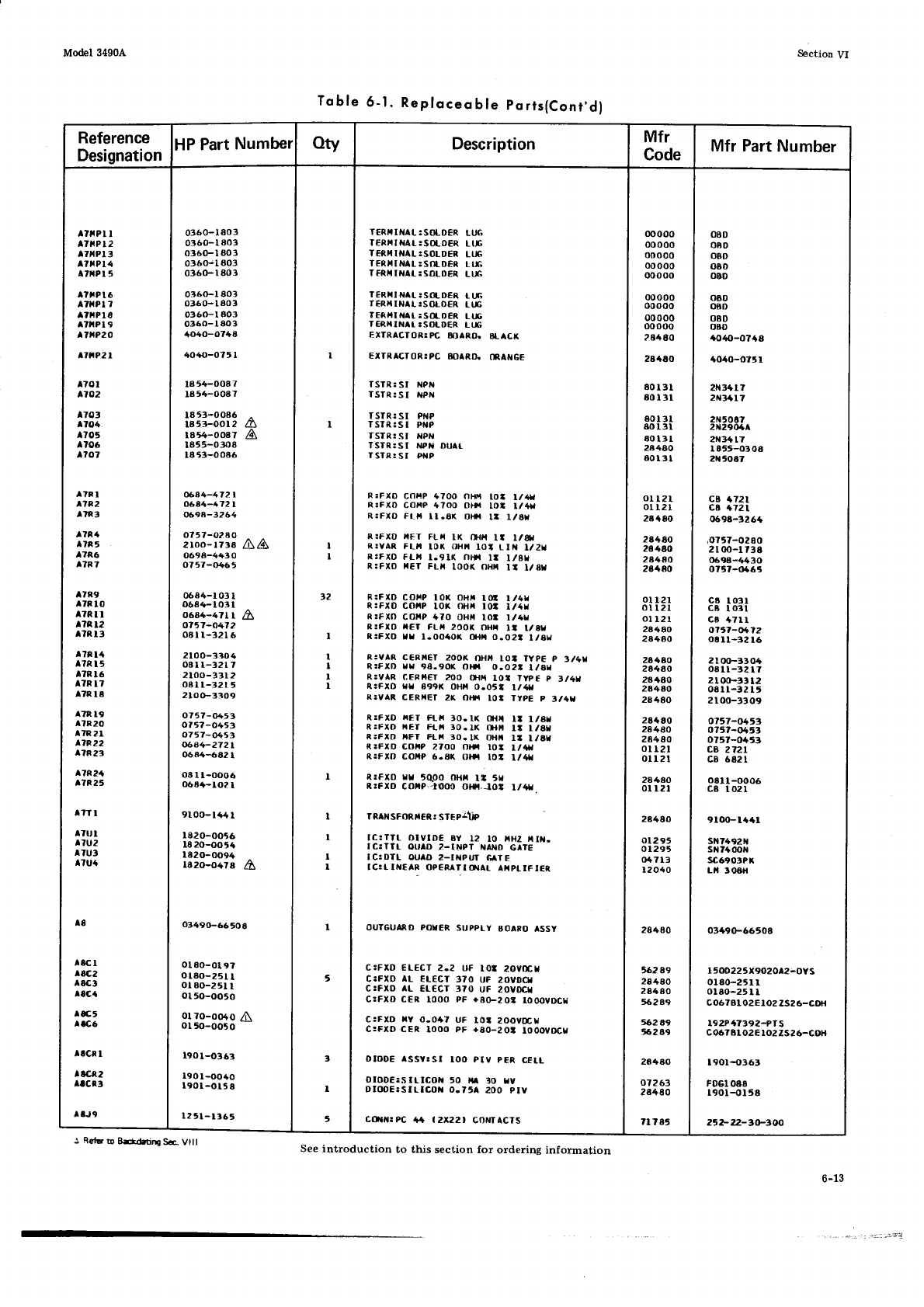
Toble
6-1.
Reploceoble
porrs(Conr'dI
Reference
DesignationHP Part
Numbet oty Description Mfr
Code Mfr Part
Number
tTfrPl I
lTtpl 2
l7t{Pl 3
l?IPl4
a?||pl 5
l?rPl 6
A?XPI
7
lltPl8
lTrPl 9
l?ftP20
^tA?21
l70l
4702
1703
1704
4705
l?o6
^707
l7r I
^7e2
ltn3
l7R4
^?t 5
l?t6
l?R7
l7R9
7n
lo
A?R
ll
l7n12
l?Rl3
^?l l4
il7R
l5
l?Rl6
A7R
17
l?R l8
A?R
19
l?R20
A7R
2I
^7e22
^7e2t
l7R2a
^7125
l?r I
lTlrl
,7U2
r7u3
l7u4
le
l8c I
^ü.2
l8c3
lSca
Ar5
rtc6
Ircn I
t'cr2
lacR:l
u9
0360-lao3
0360-l 803
0360-l ao3
036rl a03
036G-l 801
O3ar(Fl803
o:t6O- l80:l
036(F1803
0360-1803
4040-o748
40{o-o? 5 I
la54-ooa7
1854-OOa?
IA53-OOa6 ^
lstlool2 a
re*-ooar lil
1855-O30A
l8 53-OOA6
06A+-4721
o6a4-1721
0,69A-3264
o757-O2
8 0
zroo-rzaa
AA
o698-4430
O757-0465
0644-l 03
I
06a4-lo3l
o6a4-471 I
of57-o472
oaI l-:t2l 6
2 loo-3to4
08
I l-f2l 7
2loo-3:rl ?
oSll-32r 5
2IOO-3309
o757-04't
ot57-0453
0757-O45t
06A4-2721
06a4-682 I
oa
I l-ooo6
0684-lO2 I
9lo(Fl{41
1820-OOt6
l8 20-oo54
la20-oo94
1820-O478
b
A
0349(F66508
ol 80-01
9?
ol80-251 I
ol 80-2 5l I
ol 50-oo50
orzo-oo+o
I
ol 50-oo5 0
190
l-o363
190
t{ro+o
I90
l-ol5 8
l2
5l- I 365
I
I
,2
I
I
I
I
I
I
I
I
I
I
I
t
I
I
t
TCRTIilAL:SOLD€R
TUG
IERTIilAL:S(LOER
LIF
TERXINAL:SOLO€R
Lt,G
TFRI{INAL:SOLD€T
LT.G
TERIINAL:SOLDER I-IX;
TERxlNll-:S0_DER
rtE
TERXIIIAL:SOIOER
LT,G
TER|II'.^T:S(LDER LI,C
TEß.'III{AI :SOTDER
LTß
EITRACTOR:PC
B.JIR0. SLAcK
EXTRACTOR:PC
BO RD. (NAilGE
ISTR: SI NPil
TSTR:SI r|PI{
fSlR:St PNp
TSIR:SI PNP
ISTR:
SI NPN
TSTR:SI t{PN DUAL
TSIR:
SI PNP
R:FXO CnilP 47OO Ot+t tDa tt4ll
R:FXD COHP 4700 0|tt tot l/{l.
R:FXD FLt4
ll.8( Dlfl lt 1/81
R:FXD I4FT
FLX IK TI{'t II L'üI
R:YAR FL,| l0( OHX
lot LIt{ l/2r
R:FXD
FLt l..glK nl|t lt l,/8t
R:FXO
t{€T FLr IOOK OHX
lr l/8ta
R:FXD
COtP IOK OHt lot l/1y
R:FXD
COI{P
IOK (xix lot l/4f
R:FXD
COrP +70 oH|| lol l./4r
R:fxo tEr FLH 200K OHF ll [/at
i:FXO lr I.OO4O( (}t|| 0.O2t l/SrJ
I.:VAR CERIIET 2oO( OHr{ lot fypE p 3/4r
R:FXD
yr 98.90K Oltt 0.02t l/8r
R:VAR CER}I€T
2OO THH IOt TYPE
P 3,/4Y
R:FXO
rat 899t( OHx o.o5t I/4L
R:YAR CERXET 2X Orl' IOI TYPC
P 3/{T'
R:FXD
nET FLX fO.lK (l{t lt l/sl
R:F!O XEr FtH 30.1K {l{t| lt l/8t
R:FXO
XFr FLX 30.1K ftxfa
lt l/ar
R:FXD
COHP 2700 o|ft l0l l/$a
R:fxo co,|P 6.8K oHi lot l.r{l
R:FXD rt SqOO 0t{x lt 5|.
R:FXO COITP.
iOOO Olt{.JO: l/{|J
TRlNsFoRx€R:
srFplliP
lC:TTt DIVIDE ay 12 lO ltHZ
,allt-
IC:TIf OI,AD 2.INPT NAND
GATE
IC:DTL OUIO
2-IXPUT IiATE
lC:Lll{EAR OpERArlO{At-
Alip!lFtER
OUTcUARO POI'ER
SUPPI.Y
BOARO
ASSY
c:FxD ELECT
2.2 UF lot 20vm.r
C:FXD AL EL€CT :I?O UF zOVOCl.
C:Fxo ll- EI-€CT 37O UF zOVOCT
C:FXD CER l0oo PF +8(F2O: 1OOOVDCL
C:FXD
ltY 0-047 UF loa ZOOVOCU
c:FtD cER looo PF +ao-201 looovDcy
DIODE
ISSY3SI IOO PIv PER
CELL
oloDE:slllcot 50 il/l to rv
DIOOE:SILICOt O.754 200 pIV
c0ft{!Pc +1 a2x22l cor{f acTs
ooooo
ooooo
ooooo
ooooo
ooooo
ooooo
ooooo
o0000
ooooo
28480
28aAO
ao
l3l
80L3l
80131
80131
80131
24480
8013t
oll2l
ol l2l
28{80
28+80
28+AO
24480
28480
oll2r
otl2l
oll2r
2A4SO
28{80
28480
2A4AO
28a80
2a4AO
2E480
28480
2a4ao
28480
oll2l
orl 2t
2a4ao
0LI2l
28480
o1295
o
1295
o+713
12040
28480
,62 A9
2A480
28480
56289
562A9
%289
2A+AO
o7261
2A480
7l?85
(160
o8D
oaD
OBD
4040-o?aa
+o40-o751
2|r3{t?
2N3417
2r{5087
2r{290ta
2ir34t7
1855-0308
2iltoa7
ct a72l
c8 4721
069t-326{
io757-O28O
2
t oo-l ?38
0698-4430
o7t7-ot65
cE LO3l
cB lo3l
cE +7ll
o7t7-ü12
oEl.t-32 l6
2lüF3304
osll-32 lt
2l00-33t2
osll-321t
2loo-3109
o757-O15t
Of57-Ot ra
o757-0453
c6 2721
ca 6a2t
oSll-ooo6
ca lo2l
9loFla+l
sN7492r{
sttaoota
sc6903Pr
Lil 'OAH
0349(F66tO8
r 500225x9020A2:OYS
ol 80-251 I
0180-25 I I
c0678lo2Elo2 zs26-cDH
192Pa?392-PrS
c067Bt02e lo2 zs26-coH
l90l{363
FD€I OA8
l90l-ol 5a
252-22-to-tOO
o8D
o8D
OBD
o8D
OBD
Model 34904 Section VJ
l Rcft. b Bdd*ilE Sa Vill See introduction to this section for ordering information
6-13
Model
34904
Section VI
Toble
6-1.
Reploceoble
Ports(Cont'd)
Reference
Designation HP Part
Numbet otv Description Mfr
Code Mfr Part Number
^8J tO
a8f.P I
Agl,lP2
AAtlP3
A8|' P4
aal! P5
Ä8it P6
lr8ttP7
a8üP8
aai{P9
ASlr Pl 0
a8l,tP I I
480 I
l8R I
laR 2
laR 3
l8R4
AaR5
laR6
r8R 7
AAR 8
l8R9
A8R IO
A8R II
A9
A9C I
AgC2
i9l.P I
l9ilP2
A9tP3
Ä9ß1
l9R2
Ä9R3
A9R4
A9R5
r9u1
A9U2
A9U3
A9U4
AAU I
AAU?
A8W4
A8W5
A9C3
A9C4
^9C5
A9U5
t9lt6
A9U7
r9u8
a9U9
alo
llocl
Ltoc2
I lorP I
^lorP 2
l loäP l
r 1001,
rlce'-33
l25l-1365
5040-o170
5040-o | 70
5()40-ol 70
5040-o170
o349o-oi2o9
t25L-2551
t25t-2r51
t?.51-2551
t25t-255L
L25L-255t
t25t-2551
la54-o07 I
o757-O+l O
069a-4355
06a4-4221
0684-822 t
o6a4-a?21
0684-tOl I
o6a4-2231
0684- I 23 I
o6a{-l 02l
0684- lO2 I
0684-422t
l8 20-o410
la20-o586
03490-61608
03490-61604
03490-66509
ol6(F2009
o
I
ao-ol9 7
ot 60-ol 94
ol60-ol 94
ol 60-ol 94
t200-04?4
4040-o7{?
4040-0746
0684-332 I
0684- 332 I
06a4-332 I
0684- I 52
I
I
8l O-O049
I820-0584
I 820-0595
l8 20-o 584
I
820-0594
l8 20-o 546
1820-o7t
o
la 20-o 7t o
ta20-o583
t{r20-o7lo
of49 0-66 5t O
ol80-o197
ol 60-02e8
0403-c
189
o403-01
89
1200-o{?4
I 6 5r-oo? I
(}6
8{-682 I
A
A
I
I
la
I
9
2
1
I
t
2
+
2
3
2
5
3
I
t
I
2
4
CO{N:PC 44 t2x22l CONTACIS
GUIOE:PII'G.IN PC OOARD
GUIOE:PTUG-IN P.C BßARO
GUTDE:PLIIG-IN PC OIIARD
GUID€:PLI,'G.IN PC EOARD
ARACKET
: }IOUNT IIIG CONN€CIOR
CONNFCTOR:SINGLE CONTACT }1TN
IATUR,E
CONNECTDR:SI NGL€ CONTACT t{IN IATI'R€
CTINNFCIOR:SIN6LE CONIACT ilITt IAIURT
C(r.INECTOR:SINGI.€ CONTACT TIN IATURE
C0NNECTOR:Str{Gte COXtrCf |tTNIATURf
COI{NECTOR:SI N6LE CONIACT IIIIT IÄTURE
lSrR:Sl NPNI SEI-€CTEo FRox ä13-to4l
R:FXO }lEr FLx 301 oHt lt l/8L
R:FXO Fl,il 12.4 oHta l! l/8H
R:FXO COilP 8200 ot+i lot l/4U
R:FXD COttP 820C n}|l.t tot l/4ta
R:FXD CO|.|P 8200 olf{ lot l/4||
R:FXO COXP IOO Ofil{ LOt ll4|.
R:FXO COtp 22|( OHt4 10t l/4tl
R:FXD CONP lzK otlll lot l/4L
R:FXO CO|{P tOO0 ()H1 lO? l/{n
RIFXD COüP 1000 oHH lot l/4ll
R:FXD COIP a?OO Otrl lol l/4t
lC:LINEAR. voLlAG€ REGULATfTR
5V
IC:TTL LP HEX INVFRT€R
CABLE ASSY:REM
CABLE ASSYTBCD
TI6I'ARD DATA OUTPUT EOARO ASSY
C:FXD IIICA 82O PF 5l :IOOVDCI
c:FxD ELEC.T 2.2 UF lol 2oVDCH
C:FXt)
l,lY O.Ol5 ltF lO!
c3Fxo tY 0.015 trF loi
c:Fxn f.lY
o.ol5.uF lol
._l
STK€I:IC 8LK I+ CNNTACT
EXTRACIOR:PÖ.OOAROT GRAY
-
FITRACTOR:PC E0AROr 8tÄC|(
R:FXD Col{P 3300 oHM tor l/4tl
R:FXD COHP 3lOO OHI l0l l/4{
R:FXD COIP 3300 Of0{ IOA llr*l
R:FXD COtlP 1500 (1H|1
lot l/4r
RESISTIVE NETTORX:lO X 6.8K
EXTRACIOR:PC,
BLACK
EXTRACTOR:PC.
BLACX
S(rKET:lC 8LK 14 COi{TACT
TSTR:Sl NPN(S€L€CTFo
FRoll 2N3704t
IC:TTt LP OUAO 2-INPT NOR GATE
TCITTT LP DIIAL J-K I4ASIER SLAVE F/f
IC:TTI IP AUAD 2-INPT NOR GÄT€
IC:TTL J-{ I{ASTER SLAVF F/F
IC:T'L LP HFX INVERTFR
tC:DIGITÄL rrI+LOGIC 5v 5l
IC:DIGITAL ITL+LOGIC 5V 'T
IC:TTL LP OTJAO
2-INPT I{AND GATE
IC:DIGITAL TTL+LOGIC 5V 5:
NUTGUARD OATA O('TPt'T EOARD ASSY
c:Fxo ELFCT
2-2 UF lor 2oVDCI
c:Fxo t1Y
0.0015 uF lol 2oovDcti
R:FXD Cni|P 6.AK lot l/4t
7t7 A5
2AlAO
29480
2a4ao
28480
28480
oo7?9
oo779
o07?9
o0779
oo?79
oo779
2a+ao
28440
28480
ot
l2l
oll2l
oll2l
ol l2t
oll2l
24480
12040
28480
28480
2A4AO
oo853
562
89
289
$289
552 A9
2:t 680
24480
28480
or
tzl
olt2t
ol l2r
oll2l
28460
12040
l2 040
12040
t2040
12040
0726a
07262
l2 040
0726t
2A4AO
56249
56249
28480
28480
23880
28440
oll2r
oll2l
ol
l2l
ol l2t
01 l2r
a22l
a22l
a22l
IOll.
22tL
tztr
I 02l
I 02l
a22l
cB 6821
1820-o430
DxT4LOtN
03490-61603
03490-61604
o349(>66509
RDf{l 5F82
r J3C
I5m225X902042-DYS
l92P t5392-PT S
L92P 15392-Pl S
19
2P t5392-PTS '
csa2 900- laa
4040-o7t?
4040-o748
ca 332t
c8 332r
c8 l32l
c8 l52l
l8 lo-0049
Dr{74L02N
Dl|74L73N
D||?aLo2tt
o,|7{L72N
oll74L()4N
st_ 17315
sL l7:tl 5
DxT4LOOrl
sL l73l 5
0349(F665lO
Itoo 225X9020A2-OYS
192Pt52924rS
0403-ol 89
0403-0189
csa2900-l4a
1854-O07 I
252-22-t0-700
50ao-o170
5060-0t?o
5040-o170
5040-ol. ? o
o?49(FOl209
t42070
3tzom
3320?O
ttzolo
332070
3t2070
I 854-OO?l
0757-04lO
()69a-4355
CA
ca
ca
CB
c6
ca
CB
CB
ca
: ..:t'a 3:d-E Sa Vlll
i-1r
See introduction to this section for ordering information
Reference
DesignationHP
Part
Numbet atv Description Mfr
Code Mfr Part
Number
llosl
rlos2
rloul
llou2
Alou3
tlolrt
rlou5
atou6
llouT
All
allcr
^tLc2
lllc3
Al
tc4
lllc5
ll lc6
AlltaPl
lIlrP2.
AlltP3
tltot
lllFl
tllR2
ll lR3
tllR4
ll lR5
tllß6
^l lR7
rl lR8
tl lR9
/rl lRlo
lllRl I
llrul
ll luz
lllu3
Al I U/r
ll lu5
Allu6
rlluT
rl lu8
Al lu9
Allul 0
/l
llul I
rllul2
tl2
llzcl
^12c2
ll2c3
A
12rp
I
A
l2frP2
A
l2rP 3
I l2tl
^t2e2
ll2n3
r1294
ll2n5
412f,6
1t287
3l
ol-1341
3lol- l3{l
1820-0586
1820-ol
74
l8 20-o294
1820-0291
1820-029{
lazo-oz91
l8 20-0282
01490-6651 I
ol 80-o197
ol6(F2 009
ol70-o066
ol 70-o066
o
160-01 6{
ot 6{r-0294
1200-0424
4040-o748
40to-0755
r 854-O07
I
0644-470 I
0684-l O:t I
0684-332 I
()684-682I
0684-332 I
06a4-:t32 I
06E4-l 52
I
0684:642 I
06a4-682 I
068/r-6421
()6a4-6421
l8 20-o586
l8 20-o546
r820-o583
l8 ?o-o 58{
l8z(F058{
1820-o59 5
182(F0599
l8 20-o599
1820-O596
l8 20-l loo
1620-0656
l8 20-O546
0349(F66512
ol60-0154
ol6(Fol57
olao-o197
o+o:l-ola9
()+o3-ola9
1200-0{2{
la l(Foot9
068{-t521
06t4-223t
06'34-22a1
06t+-lo:tl
o6a4-l 03l
(16E+-lo3
I
A
A
A
A
A
4
IlN
A
A
A
2
+
?
I
2
ll
I
7
I
I
I
sttrcH:sLtDE SPDr O.5A l25V ACIDC
SIITCH:SLIOE SPDT
O.5A t25U ACTDC
TC:TTL LP H€T II{VERTER
IC:TIL HFX II{YERTER
IC:TTI.8-6IT S€R-III PAR
oUT shlFr REG
IC:TT! A-BII SER.IN PAR
OUT SHIFT REG
IC:TTI A-6IT SER-IN PÄR
oUT SHTFT REG
IC:TTI a-8lf SER-m pAR our SHIFI REG
IC:TTL OUAO
z-INPT EXCL. OT 6ATE
II{GUARD
RE'IOIE ASSY
C:FXD
ELtCI 2.2 UF lot 2OVtEl
c:FxD filca a20 PF 5! toovDcr
C:FXD XY 0.027 UF lot 2OOVml
C:FXO t|Y 0.027 UF lor 2OOVm,r
C:FXD
xY O.O39 UF lot 2OOVmr
C:FID raY
O.OOlt UF lot 2OOVOCII
-SOC(ET:lC AL|( 14 CONTACT
EXTRACTOT:PC AOAntL ilt
aCl
EITRACTNR:PC
MIARDT
VIOLEI
rstR: Sl NPli( S€l-ECTFD
FßOti 2r{3?O4t
R:FXD
COrP
47 oHX lot l/4t
R:FXD COIiP
IOK OHX
lot r/41
R.:FXD
COflP 3fO0 0t0a rot l/ata
R:FXD COIIP 6.A|( O|rl lO: l,/al
R:FXD COLP 3300 oHx rot l/{ta
R:FXD COXP 3300 otil lot l/{l
R:FID COI|P ItOO Oil. lot l/al
R:F!D CO|P 6.AK Olta IOt t/tl
R:FXO COraP 6.8( Ot{a lot l/4|a
R:FXO COilP
6.8r, Otfi lot l/4r
R:FXD COftP
6.8( Ot+t lot l./4u
IC:TTL IP HET II{VET,ER
TC:TTL LP }€X IIIVERTER
lC:ltl- LP qUAo
2-Iilpr NAN0
6lTE
IC:TTL Lp OIHO 2-t*"t NOR
c^l€
tc:TTt LP otllD z-II{PT uor erie
lc:rll [P nral J-x xlsr€R st_tYE F/F
rG:TTL 4-Btr rrttt sxtrr RE6ISIER
TC:TTL '-BII TT/LT SHIFT REGISTER
IC:TTI LP DUAL
EDG€
TRT6, o F/F
I C: fll
ICsTIL LP +-AIT 2-INPT XULTIPLEXER
IC:TTI. LP HEX
INYERTER
ourculRo RExorE 80lRD assY
C|FID lllcA ttY O-Oo22 UF tot 2OOVDCI
CsFxD tY O.OOi? UF lot zOoH)CI
C:FIO ELECr 2-2 uf lO! ZOy(E,ta
EITT,ACTORSPCr
BLACI(
€XIß.ICTOR:PC' SLAC|(
S(E(Ef:IC BLf, lt CA]i|TACI
RESISTIVE
NETIORTSIO
I 6.8X 0t{t lot
R:FXO CO||P ISOO Ottl lot t/ar
I:FID COI|P 22K o.tx lot l/tl
R:FIO COüP 22t( OHX
LOI l/4r
R:FID COI|P lot( (l|ilt lot l/tta
R:FXD COI|P tO( OHX lot t/at
R:FID COXP IOX (}tX lot l/41
79727
79f27
12040
ot295
12040
l2 040
1204{)
t2040
01295
284aO
562A9
0o853
562A9
562A9
562 89
56249
23880
2A4AO
2E480
28480
or
l2l
ol
l2l
0112 t
otr2t
olt2l
ol tzl
oll2l
oll2l
oll2l
or
l2t
oll2l
l20to
l? oao
l2 oto
120{o
l2 040
l20a{t
t2 0to
l20ao
12 040
01295
01295
12040
284EO
56249
56289
249
28480
?B4aO
oll2l
ol r2l
0tt2l
0l l2l
0ll2l
oll2l
284aO
23880
c-ll l-ooo4
c-ll l-ooo4
D,|74LO4N
sx7404r{
slr9935
so9!r35
so9935
srxr!135
sN7a86ll
o:t{9{F66511
1500225X9020A2-DYS
RDIll5FA2lJltC
t92P271921t5
t92P27t92-PtS
192P39392-PTS
192P 15292-?lS
csa2900-lt6
4040-o?48
40ao-o7tt
r 8't-oo? I
CE
ca
c8
cc
CB
CB
ca
c8
c8
c8
+?ol
I
03l
3321
6a2l
3t2l
3321
I521
6821
6821
6A2l
6821
DrT4LOara
oriTaLotll
?2rl
22at.
I 031
l03l
lo3t
Dt|?4t-ootl
otTtL02t{
Dl|7{L021{
Dlt?+L7tfl
oä7{L9til
Dt?4L95tl
Dlt/tL7tr
sN7a29t
sl|?4L9tt{
ot?aLo+ll
03a9(F65tl2
t92P2?2t2-?lS
192Pa?292-PrS
Ito22tr90?oa2-DYs
o40t-o189
(rGt-olr9
csl2900- la8
l8L(H)Oa9
cc lt2l
c8
c5
CB
CB
ca
Model 34904
Toble
6-1. Reploceoble Porrs(Cont'd)
Section VI
l RdEbBdätiESaVill See introduction to this section for ordering information
6-lä
ModeI 34904
Section VI
Toble
6-1.
Reploceoble
Ports(Cont'd)
Reference
Designation HP
Part
Number otv Description Mfr
Gode Mfr Part Number
Al?ul
^L2u2
AI2U3
At2tt4
^l?u5
^13
al3cl
Attc2
Al3C3
al3c4
a l3cR I
a l3cR 2
Al3CR3
I l3CR
4
al3cF6
AI3CR?
AI3CR
8
al3riP I
l l3r,lP ?
l l3tlp 3
a
l3ltP 4
a l3xP
5
al.3r,{P 6
a l!ll.P 7
l13R I
AttR2
A
I3R3
I l3R4
AI3R7
A
l3R8
a l3ß9
,allRlo
AI3RI IA,
R11B
al3Fl 2
Al3Rl3
al3Rl4
Al3Rl
5
al3Rl
(
Ä
l3Rl
7
ll3Rl €
al3R I 9
a l3Ul
AI3U2
AI3U3
AI3U4
Al3U5
ll5
ll5rPl
ll5ul
rltu2
I
l5u3
I l5L4
rttL:
^15!6
1820-o
70 8
la20-o 584
1820-o595
I 820-Or
2 I
t8
20-0 32 A
03490-665 I 3
ol 50-c 05 0
ol 50-o093
ol 50-0093
0180-0197
l9 02-067 I
I90
l-o5 86
I
90 l-o5 86
190
2-o6? r
t902-3 190
1902-3 190
19 02-1to8 5
t200-o424
4040-0748
4040-o154
1200-o
43?
l2 00-043 7
1200-0437
t200-0474
o8 l3-o032
06a4-2f11
0684-27:Jl
o698-7962
2100-3305
2roo- 3305
069A-4202
o751-O277
08 I t-f?23
2roo-f3 1 4
0698-a2 7 t
2loo-33 t 3
0757-O442
o7 57-0378
2loo-3305
06
84-392 I
2lo(F3305
la26-0 I I O
t826-Ol I
0
1826-0t tO
LA20-O22
3
182(F0598
03490- 60306
03490-04 l.l 5
1990-o40 2
I
S90-0402
199
0-o40 ?
199(F0402
1990-o
40
2
1
9 90-0402
2
I
2
I
2-
I
2
2
2
I
4
I
I
I
I
I
I
t
2
I
I
36
IC:TTL LOTI POT€R Di,AI 4-INPT XUITIPLFX
TC:TTI fP OUAD
2-INPT NOR GATE
IC:TTI LP DUAI JJK }IASTER SLAVE F/F
TC:DTf HFX INVERTER RL:2X
IC:TTf OUAD 2-INPT NOR
GATE
RATIO REF€RFIICF SOARD ASS{
c:FxD CFR looo PF +8o-2ol lOOOvDCl,
c:Fxo cER o-ol uF +80-201 toovDct{
c:FxD cFR O.Ot UF +80-20t 100VDC.y
c.:FxD ELEC 2.2 UF 10% 2oVDCW
DIOOE BREAKDOIIN
DIODE:SI 30 t,'V IO PA LEAKAGI
DIODE:SI 30 HV IO PA L€AKAGE
OIODE AR€AKDOTN
DIODE 8R€AKOOTN:13.0V 51 400 llll
DIODE AREAKOOIiNT13.0V 51 400 fit
DtoDE ßREAKOO||N:4.?5v 51 400X|'
SNCKEI: TNIFGRAT€D CIRCUIT 14 COXIACI
€XTRACTOR:PC AOARO' BIACK
EXIRACTOR:PC 8f|ARor SLUF
SOCKET:
IC 8 PIN
SOCKET:
IC 8 PIN
SOCKFT:IC 8 PIN
S()c(Et: lC l4-PIN
R:FXo lH 50( Ol{l{ lol 5t
RIFXO COr,rP 2tK,nHil lot l/4L
R:FXD COiIP 27K OHt{ l0l I/{H
R:FXD.FtN 976K-gH'l l.O! l/SY
R.:VAR 00K Oti{ lol 3ltll I/2 ruRN
R:vAR CfRltEt('looK oHl lOl 3/4tl l/2 TURN
R:FXD Ffr{ 8.A7K nfr{ lt r/81
R:FXO ltFT Ftf4 +9.9 0}}t tl l/8v
R: MATCHED SET
R:VAR CER{€T 50 Orfi l0l IVPE P 3l4r
R:FXO TiETAL 6LAZE t.l OHll 5t l/41,
R!V^R CERHET lO0 (}{h lot TYPE P 3/+l
R:FXO HET FLf{ lO.O( 0+il{ ll l/81
R:FXD ltET FLI ll.O oHlt M/8|
R:VAR CERf|ET l00K {lHr.t LOa )l4|t l/2 ruRN
R:FXD COI{P 3900 0H,t LOr. lltl
R:vAR CERIET loOK OHä lo, tl41 1/2 rURil
A
TPL.
GAIE
lC!t.lN€AR oP. A+tPL.
IC!I.INEAR OP. A}tPL.
IC:LINEAR OP. AilPL.
I I{TEGRAT€O C I
RCI'I T!OPER
ATI(}"IAL
IC:TTL LP OI,AO
2-INPT FXCI. OR
OAIA üJTP('T ISOLATION ASSY
PLÄTETTI HO('NTING
T STR: PHOTO
TSIR: PHOTO
TSTR: PHOTO
TSTR: PHOTO
T STR:
PHoTo
TSTR: PHOIO
o7 26t
l2
040
t2040
04? l:i
04?13
28
480
'6249
729A2
72942
56289
2a4 80
2A4AO
28{80
28480
28480
2a{
60
2A480
23880
28480
2
8480
l?ll7
l7l lt
lTll?
?a4ao
2a4ao
oll2t
oll2t
284
80
28480
284AO
?-a4ao
28480
?8480
28480
2A4AO
2A4AO
28480
2A4AO
2a4AO
01
121
2A4AO
28480
28480
2844O
24480
12040
284 80
28
480
28480
2a480
28
480
24480
28480
28180
u6891-O959X
Dt{7{LO2N
otl?4L73til
Lc837P
sN?402N
03490-66511
c067
Blo 2E
lo2zs26{oH
801-|(80001
t
ao
t-K80001
I
1 50D225X9020A2-DYS
1902-0671
l90l -o586
l90l -0586
I 902-06?l
1902-31
90
1902-3
190
1902-!005
csA290G14B
4040-o7t I
4040-o?54
5566-2t5-5
5566-2:,5-5
5566-275-t
1200-o{74
o8l3-o032
co 27rl
cB 2731
69A-7962
2l oo-3305
2 I 00-3305
0698-+202
o757-O277
06tt-122,
2too-)ll4
0698-a2? I
21 00-33 I 3
0757-O142
075?-0376
2 I OO-330
5
cB 3921
2t oo-3:t05
1826-Ol
lO
1826-0l I O
1.826-0l I O
t820-o221
Dfi?4L46il
0349G-60306
0349(FO{l l5
1e9o-O+O2
1990-oto2
1990-o402
1990-o+02
1990-0402
1990-ot0 2
See introduction to this section for ordering information
Model 34904 Section VI
Toble
6-1. Reploceoble
Ports(Cont'd)
Reference
DesignationHP
Part
Number otv Description Mfr
Code Mfr Part
Number
A I'AI
arSl lo I
al5al02
ll5alo3
alSalc4
ll5Älc5
al5alc6
AL5!l8l
tl5tlR2
elSllR3
Al5Aln4
tltalF5
ll5alR6
lt5at14
At5A2
ll512Rl
^t5^2R2
It 512ß3
Al5A2 R4
tt:tz*s
ll5r2R6
ll 5l2r 5
^17
Al?xP
I
^l?ul
AI?U2
ll7ul
Al?ua
^17u5
tl?u6
Al?al
llTalo I
tlTtto2
AlTrloS
rlTat ßl
Al?al n2
lltll R3
Ä17^tß4
al.7Al R5
alTal ß6
A lTll 16
A
I7A2
Al7A20t
At? 4202
al71203
A l?Ä2R
I
At? L2R2
AL?
t29t
r l712n4
ll ?t2r 5
^l ?^2 nö
ll?rzl?
03490-6651
5
1854-OO7
I
l8
54-OO t I
l8
54-OO7
I
1854-O07
I
l8 54-OOt I
I 854-O07 I
06a4-47 0 I
0664-4701
0684-+70 I
o6a4-4701
06a4-470 L
0684-470r
8120-1855
0349(F66516
0698-4 l2 3
069A-4t2:,
0698-4121
069a-4123
0698-4123
0698-4123
8l 20-18 5
5
0349(F6030A
03490-04l l6
1990-o402
199(F0402
1990-o402
1990-0402
1990-o402
199(F0402
0349(F6651?
1854-O07
I
1854-O07
I
1854-O07l
0698-4 I 2 3
(}6a+-4701
068+-4?O
I
o69a-+123
0698-4123
o6a{-4701
al 20-l 855
03490-6651 I
l8 54-OO
7t
1854-OO7
I
l8 54-O07
I
0684-470 I
069a-412 3
o69A-412
3
0684-4701
06a4-470 I
0698-41 2 3
al20-1a55
I
t
I
l2
I
I
INCTIA&D
BCD ISOLATTOII BOARDASSY
TSTR:Sl NPilISELECI€D
FROt A,r3?041
TSTR:Sl NPtiIISELECTED
FR,Oit
an3?O{l
ISTRTSI NPNISELECTED
FROT
AI37O4I
TSIR:SI NPNISFLFCTED
FROfi
2I{3704I
TSTR:Sl NPN|
SEI_ECTEO
FROit
a{3?O4'
TSIR:Sl NPr{lS€LECTED
FROil
an3?O4t
R:FXD
COf,tP 4? OHfi
lot l/4li
R3FXD
CO|{P 47 oHtt lot l/41
R:FXD CO|{P 47 oHil lot l./4ta
R:FXD
CnHP
47 oHn lot t./41
R:FID CO!{P 47 ot{a{
101 t/4H
R:FXD
CO'{P 47 oHX lot. l/{l
CABIE:RIEAON
OUTGUARD
BCD ISOI.ATI(rI BOARDASSY
R:FID XEf FLX 499 (]Hl| lt t/8t
RiFXD f{€T FLX 499 OHta
lt t/8r
R:FXD ltEr FL'l {99 oHti l! l/ar
R:FXO r,tET
FLft 499 oHfi lt l/8r,
R:FXO irET FLt 499 oHr{ l! l/8I
R.:FXD xET FLll {99 OHü lt l/Ol
cAEt_E:RtBB0r{
REilOTF ISNIATION ASSY
PLATE:LI T.(UNTINc
TSTR,:
PHOTO
T STR: 9r{oTO
fSfR: PHOTO
TSTR: PHOTO
TSTR: PHOTO
TSTR! PHOTO
INGUARD
R€i..IsoLATIoN BoARD
AssY
TSIR:Sl NPt{l
SETECTED
FRoil 2il37o41
TSIR:Sl t{PNaSELECTEO
FRct An3t0{t
lsrR:st NPN|s€LEct€D
FROi at3704l
R:FXD nET FLH
{99 oHil tt l/81
8,:FXD
COI{P 47 oHft lot l/41
R:FxD CoitP 17 OHtt lot l/al{
n:FXD HE.r FLH
{99 OHt{
l: l/8y
R:FXO ||Er FLr 499 oHr{ lt l/ol
R:FXO CONP
a? OHtl
lot t/4lt
CAELE:RIAEON
OT'TGIITRD
REI{ ISOLATI(}I BOARDASSY
TSrn:Sl NPNISELECIFD
FROr 2N37O4l
TSTR:Sl NPN(S€LECTED
FROr an37o4l
TSIR:SI llpl{tSE|_ECTEO
FROI| an3ZO{l
R:FXD COrP
47 oHlr lo: l/4r
R:FXD ftET FLll 499 oHli lt l./sr
R:FXD ||ET FIr{ 499 oHH lt t/81
R:FXO COrlP 4? OHlt
lO! l/4r
R:FID COtiP 47 (l|{l{ lot l/4r
R:FXD LET FLll a99 OHn lt l/8f
CABLE:RIBBON
28a80
28480
28480
28{80
24480
2A4AO
2a460
ol
l2l
oll2l
oll2l
01 l2l
01121
0l l2l
28440
2A4aO
2a/T80
2E480
284r0
284 80
28480
28440
28aao
2A4aO
28480
2a{80
24480
2A4AO
2A4aO
28480
2844O
2A4 80
284a0
286r0
24480
28180
ol
121
oll2l
28480
28480
oll2l
28480
24t80
28480
28a80
24480
ot l2l
28480
28480
0tr2r
ol l2l
28{80
28480
o:tt9(F66515
1854-0071
18't-O0? I
I I't-00?t
1654-OO7l
I 85r-0071
I 854-00? I
c8
c8
co
CB
CB
c8
4701
t?ol
4701
4?Ot
4701
4701
ot 20-t 85
5
(I:|+9(F66516
0698-tt 2l
0698-6t2t
0698-{l 2:l
0698-4123
o698-4t2t
0698-{123
al20-l 8t5
o3t9(F60308
o:ta9(F04l16
I 990-0402
1990-0402
1990-0402
1990-oi02
1990-oto2
1990-oto2
ot49(F5651?
1654-OO7l
I 854-OOtl
1854-00? I
0698-412!
cB a70t
c8 4701
069A-4123
o69a{123
cB 4701
8120-1855
03a9(F66tla
I 8t4-O0? I
1 854-OO? r
l8*-oo7 t
c8 4?01
069A-{123
0698{123
c8 4701
cB 4tol
069A-{123
at2(F1855
See introduction to this section for ordering information
6-l?
Section VI Model
3490A
Toble
6-1.
Reploceoble
Ports(Cont'd)
Reference
Designation
HP Part Number otv Description Mfr
Code Mfr Part Number
422
A22AP I
^22U1
A22U2
^22 Al
122Äl R
I
^2
2
^tF2
a?2rlut
A22 A2
22^2Cl
^22^242
^22^2Fl
422^2F2
424
A24rP I
A24|/.P
2
,24e1
^25
^25AP I
^254P2
426
^26XP
I
A26r4P
2
A26AP1
^27
a2
7Cl
427C2
^27C5
427C6
^2'tc7
A2fCA
427C9
^27CtC
l27C
I I
^?1
Ct
2
l2?c
l4
L27Ct5
^27Ct
6
^27
Ct 1
^27Ct
€
127C
I 9
r27;t I
r27Ct
2
03
490-60 302
03490-04l l4
1990-o40
2
1990-0402
01490-6652_2
0684-a22t
o6a4-lo2 I
t820-0586
o3+90-66524
185+-OO? I
l8 5 4-OOl
I
06a6-470 I
0684-470 I
ot490-66521
4{r40-o748
4040-o"152
0698-OOA{
03490-6t 525
4040-0744
4040-o75 3
ot490-665?6
I 2 00-o76
a
4040-o748
4040-07 5
/r
01490-66527
ot
60-2
I 98
o
160-2 l9 8
01 80-ol 9?
otao-ot97
ol 80-0197
olao-ot97
ol 60-0679
o
t60-i85 5
ol 60-3
077
ol60-1tl 9
ol60-2199
ol60-3622
ol 60-1
t 83
o160-2199
ot 60-31
83
ol60-2t99
t90
1-oO40
190
l-00{o
I
2
I
I
2
I
I
2
I
I
2
I
SYSTEIl I SOLAT
IOI{
PIATE:SYSTFX LI
rSTR: PHOTO
ISTR: PHOTO
INGUARD SYSIET ISOLATIOiI BOARD
ASSY
R:FXD COIP 82OO O|t{ tot l/4ta
R:FXO COarP 1000 ortt lof l/4t{
IC:TTf LP HEX II'IVERIER
OI,TGI'ARD
SYSTE}I ISOLATION BOARDASSY
f stR:sl NPNtsEl.EcrED FROt{ An3704t
TSrR:SI NPNIS€I,ECTEO FROI' 2N3704l
R:FXD COflP 47 oHh LOt l/4t
R:FXD COI{P 4? OHF tot I/tta
S/H ANALTE JU'lPER ASSY
txTRACTOR:PC 80ARO. 8t_AC(
FXTRACTOR:PC 80ARO, YELLOT
R:FXD I'ET FLil 2.I5K fHil It I/8II
S/H LOGIC JUI{PER ASSY
EXTRACTOR:PIC
8{)ARD, 8f ACx
EXTRACf.b{:PC .8o^-Ro. GREFN
RATIO JI'IIPFR ASSY
SOCKEI: INIEGRATED CIRCUIT 14 coNTAcI
EXTRACTOR:PG BOARDT ALAC(
EXIRACTOR:PC 8OARD. SLUE
SAXPLE/HOID ANALOG AOARD ASSY
C:FXO ltlcA 20 PF 5l
C:FXD IICA 20 PF 51
C:FXD ELECI
2.2 t,F loi
C:FXD ELFCT
2.?.
UF IoI
C:FXD
ELECT 2,.2 IJF IOZ
2ovDct
20vDct
20vmr
c:FxD ELFCI
2.2 UF lOt 2oVOCI
c:Fxo IEFLOil 56'JO PF 5r l00vDCta
c:Fxo P0LY 5600 PF 5t 1ooVOCn
c:Fxo HY
0.027 UF lot loovDcr
c:Fxo o.l trF l00vDci,
c:FxD Htca 30 PF 5t tooyDcr
c:FxD cER O.l UF +80-20! IOOVDC|'
c:FxD t{Y
0.47 UF zCt 50VDC|
c:Fxo Hlca 30 PF 5t 300vDcl
c:FxD f,iY
o.+7 trF 20t 5ovocP
C:FXD llCA 30 PF
oInDE:SILtCOt{
50
DIODE:S
ltICnil 50
5t 300v
ocr{
xa 30 9v
taa 30 rv
284
80
28480
28480
28480
2A4AO
ol l2l
oll2l
12
040
2A4AO
28440
2A4AO
oll2t
oll2l
24480
28440
28480
2A4AO
28480
284 80
28480
28480
9I506
28480
2A4AO
284AO
72t36
72t46
562 89
562A9
562
89
56259
2a480
284A0
562 89
28480
28480
729a2
a44tl
2a4AO
84411
28480
o7263
07263
o:|49(F60302
o349(FO4t l4
1990-0402
1990-0402
0349(F66522
cB 8221
c8 lo2l
Dat74LO4t{
03490-66523
l8 54-OO7
I
I a54-O07
I
ca 4701
cB 470t
0749(J-66524
4{)40-o?48
1040-o752
0698-OOA{
0349(F66525
4040-o748
4040-0753
03490-66526
3r4-aG5D-3R
404{)-o748
4040-0754
o1490-66527
ROfll 5C200J3C
ßot1l 5c
200J3c
t50D22
5
X9020A2-DYS
l5 o 22 5XeO20A2-OYS
l5 0D225 X902042-OYS
I 5 ü)22 5 X9020A2
-OY
S
ol60-0679
ol60-1855
225P 2739t$t-PNA
ol60-341 9
ol 60-2 I 99
8l 31
-l OO-65 l-l 04Z
HEI' IOI
ol
60-2
199
HFH 1O1
ol 60-2 199
FDGI 088
FD6l 088
See introduction to this section for ordering information
Model 34904 Section VI
Toble 6-l. Reploceoble
PortslCont'd)
Reference
Designation
HP Part
Number aty Description Mfr
Code Mfr Part Number
^27CR 3
^27C41
A27CR5
^27CR6
A27CR1
l27CR
8
)27Ct9
a2?cR
lo
A27CRt2
A27CR l3
a27CR l4
A??CR I 5
i2?ca l6
lz?cR I 7
A2?CR l6
A2?CR l9
A27CR 20
^27CR22
^27CP23
^27CR21
^27CA25
^27Ce26
^27tR27
l2?ßl
^27K2 .
A27l-
I
427L2
l2?13
^27L4
A27rP I
A27AP2
^27nPt
t27tP4
A27rrP5
^2ZOl
^2702
42703
^2704
^2705
42706
^2707
A2708
A2?O9
42701
I
A27R
I
A27N2
A2?R3
427R4
A2?R5
Ä27R6
l2?R8
427R9
a2?nl
o
l27Rl I
A27Rl
3
127Rla
t2?Rl 5
A2?RT
?
^z'tR t I
Ä2?R
I 9
427e20
A27P,2l
^27F,22
Ä27e,23
^27s21
^27t25
^27e28
l2?F29
^27R30
1901-o376
l90l -oi76
190
l-o376
l90l-0376
190
l-0040
l90l -o376
190 l-o176
1901
-037
6
leo
2-3
180
1902-3
I
8 0
190 l-oo40
190
l -o376
190
t-o376
190?-3 I 9
I
1902-3
r9 I
l90l-037 6
190
t-o376
I
901-0376
190
2-l 19 I
1902-31
9l
t90 l-o 37
6
l90l-0376
190 l-o376
o490-o373
o490-o373
9t ?o-0894
9l 70-oa94
9l 70-0494
9 t 70-o894
4040-074A
4(}40-0752
1200-o4t7
1200-o4?4
0340-o060
1855-0093
la55-0304
la55-oo9 3
I I 55-O093
ra55-009:t
I 455-030a
1855-O09
l
l8 54-02 I 5
la55-o003
l8 55-O:!41
0757-O28
0
0757-O27t
2t oo-2{a9
o698-+460
0698-3!r5
2loo-31o3
o?57-O{49
o757-()4+9
075?-O453
o757-0442
2
loo-3306
2l oo-33 I I
o?5?-0449
0757-0449
0684-4?3 I
o6E4{?31
0698-4505
069A-4505
0698-f9.5
075?-o4t8
o7t?-o4:t8
o7
5?-0+65
0757-()449
o?57-O43
I
o?57-()465
t5
2
2
I
I
I
2
I
DIODE:SILICON 35V
DIOD€:SILICON 35V
DIODE:SILICON 35V
oloDE:slLlcoN 35Y
DIOO€:SILlco|| 50 llA 30 lV
DIODE:SILICON 35v
DIODE:S
ILICON 35Y
DIODE:SlLlCOt{ 35V
DIOOE ARFAKDOI'N:
II.BV 2I
olooE aREAKDO$I:ll-8V 2l
DInDE:StLICON 50 lrA 30 tv
DIOD€:SILICON 35V
DIOOE:S ll-ICON 35V
DITJDE
BREAKOOIIN:
I3.OV 2I
DIOO€ BREA(DOtr{: l3-OV 2t
DIOD€:STLICON:}5V
DIoOE:S
ILICOI 35v
DIODF:SILICON l5V
DIODE BREA(OOyN:13.0V 2t
DIOOE AREAKDOr.f{:
l3-OV 2t
OIoDEss lLICOri 35v
DIODE:SILICON 35V
oloDE:s ILlcoN 35v
RELAY:RFET)
REI.
AY:R F FN
EEAO: SH I Et DI N6
BEAO3
SH I
ELO
I
NG
R€AD: SH
I EL DI iIG
BEAT':
SH I EI.D
I ilG
EITRACIOR:PC AOAR
D' BLACX
EXTRÄCTOR:PC AOARD. YELLOI
Sü:(ET:IC A PIN
soc(€T: Ic l4-Plra
FEEDTHRU : INSULAT€ D Tü'NT ING
rSTR: FET THHANN€I.
TSTRsSI NPN DT,AL
TSTR:FEI N{HANN€L
ISTR:fET N-CHANiIEL
TSTR:FET N.CHANNEL
TSTR:SI TIPN DUAI.
lSf R: F€I l{-CHAI{NEl-
TSTR: SI NPTI
f Sf R: FEI tl-G{tAlMt .-i
rSfR:Sl FEt N-CHAM{El.
/.'
R:FXD IET FLfr lK Oil. lt t/al
R:FXD ftET Ftr 3.OtK ürrl lt t/8t
R
:V/lR FLfi 5( (ttft lo! L
I it 1/21
n,:Fxo FLH 649 oHf{ lt 1/81
R:FXO
r{ET
FLt 34a OHt lt l/81
ß.:vaR cERfrEl loK &rr lot Typf p 3/4r
R:FXD Ft-l{ 20|( fl.ilt lt l/8h
R:FXD
FLX 20K
OHtl
l: l/Eh
R:FXD
l|ET FLll :tO.lK fItX lt l/8X
R:FXO r{ET FLX l0.O( O{lt lt l/al
R:YAR CERXET 5OK (Hli lol rYPE p 3/4ta
R:VAR C€RtEr 500 a*ilt lot TYPE p 3/tI
R:FXO
FLX 20X OH||
lt l/8r
n:Fxo FLt 20K oHx tt l/8y
R:FXD
COI{P
47K OHI{ lol l/{L
t:FxD colrP 4?t( oHfr lot l/al
R:FXD t{ET
FLll 7l-t( $tr lt l/8ta
R:FXO XFT FLlr 7l.t( 0fili lt I/Ar
R:FXO
r|€l FLI 34a OHl|
l: l/8r
R:FXO
llEl FLt 5-llK OHl,l
lt l/8r
R:FXD
tET FLX 5.11( tltit lt t/8ta
R:FXD l,lET FLll IOOX Olfl ll l/Sa
R:fxD FLfl 20( ()|il lt l/aY
n:FxD ltET FLx 5.llK ülft ll l/Ar
R:FXO
||Et FLt IOOK
(x{i lt l/ff
600 Hr
400 tr
2A4AO
28S80
2E480
284 80
0726A
284 80
2844O
28480
2|N4AO
28480
07261
28480
2844O
28480
zA4AO
2A4AO
28480
28480
264AO
2844O
2E460
28480
28t80
2A4AO
28460
28+ 80
28460
2 8480
28480
28480
28+80
.l7l l7
28480
28480
28480
28480
2A4AO
24480
2A480
2a4ao
28480
80131
24480
t1127
zA4AO
28480
28480
2A480
20a80
2A480
28480
24t80
28480
28480
28480
28480
28480
24480
otl2I
oll2r
28480
28480
28tAO
2At80
28480
28480
28480
24480
24t80
l90l-o376
190l-0376
l90l-o3?6
l90l-0376
FD6l 048
l90l-o3?6
l90l{376
l90l-o376
1902-31EO
1902-3lao
FDGI 088
l90l-o3?6
t90l-o376
1902-319 I
1902-31 9t
l90l-o376
l90l{)3?6
l90l-o376
1902-31 9l
1902-319 I
I 901
-0376
r90l-0376
I 901
-o3?6
0490-037t
0490-0373
9l?o-0894
9l ?o-o894
9170-oEgt
9t ?0-0894
404{FO748
4040-0752
5566-2t'-5
1200-oa76
0340-0060
1855-O093
I 855-030A
1855-OO93
la55-oo93
1855-O093
lE55-030r
la55-o$r3
2N3904
1.855-0O93
2t{4338
0757-()280
075t-o27t
2l o(>2449
069A.*60
069a-3445
2loo-31 o3
o?5?-o{49
o75?-O449
o?57-0451
0757-O+12
2100-3306
2l oo-33 1 I
075?-0t{9
o7t7-ott9
cB 47tl
cB a?31
0698{505
0694-+tO5
069r-3445
o75t-0438
.o?t7-043 I
o757-()465
0757-().49
0757-O+3E
0757-{t465
See introduction to this section for ordering information
6-19
Section VI Model 3490A
Toble
6-1. Reploceoble
PortslCont'd)
Reference
DesignationHP Part Number Qtv Description Mfr
Code Mfr Part
Number
Ä2?R3
I
^27P.a2
^27R33
A27Rt4
^27Rt5
427R36
427R3?
427R3
€
l2?R19
127R40
427R43
^27F'44
zfe4t
^27?16
^27R41
12?u
I
^27U2
27U3
427U4
^27U5
^271t6
427U7
^27üA
^27U9
A2?UlO
428
^2acl
a2ac2
^24c3
l28Cß
I
l2acR 2
^28lrP
I
^?AAP
2
^28tP)
t2araP4
a28XP
5
Ä2 8tP 6
1280 t
A2AR
I
428R2
r28R3
A26Ra
128R
5
Ä28R6
428R7
a2sis
a2an9
A28Rl0
l28Rl I
428ß
I 2
a28Rl
3
a28Rl
4
a28Rl
t
l2a ul
^zau2
l?6u3
A2AtrI
12ar,,.
^2 CrtS
r2aJ6
^24i7
o757-0149
o757-O40 I
075T-0r'r65
0698-3162
0757-ü42
o757-O401
069A-3 I 62
0698-450 5
0698-4505
068+-47:r t
0757-0449
o75?-O438
0757-0449
o757-0449
06a4-473 I
I
826-OOt9
1826-OOl
I
1826-OO59
1826-OO59
l8 26-0O2
I
1826-OOt
9
1826-0O59
1820-t02 I
t820-t()2r
1820-ot 74
0349(F6652I
ol 60-3077
ot 50-ooa4
ol60-260 5
190l-o5l 8
1902-3183
4040-0748
4040-o753
t200-0F.74
1200-o47
3
1200-0469
o3ao-o8
32
la 5{-oo7 I
0684-t O3
I
0684-332 I
0684-562 I
0684-682 I
0684-lOt I
06a4-3321
0684- l03 I
068+-562 I
ta lo-oo50
tSto-oo50
o6a4-56?,1
06a4-562 I
o757-O116
o75l-O2A)
068a- lo2 I
Ia2(FO5a3
tE 20-o65 8
I 820-0596
l8 20-06 5a
182
0-0656
lE 20-o6 56
162
(FO708
It 20-o47 I
4
I
I
3
2
5
I
2
2
R:FXO FLH zOK OHH lt l./Ar
R:FXD ilET FL|| IOO OHri tt l./8tt
R:PXO äFf F|.r| loo( oHa lt t/a.
R:FXD IET FLX 46-{( Otil lt l/8r
R:FXD |lEl Fl-fl lO.O( (I{lt l: l/Al
R:FXO HET FLx IOO OHra
t! l/gy
ta:Fxo l|FT FLfr 46.4|< OHI ll l/8r
R:FXD t{ET Ftt ?l.5K (l{H lt l/ara
RsFXD ltET FLlt ?I.S( OHtl ll l/81
R:FXD COI{P 47K 0H|| lot l/41
R:FXD Ffr{ 20( 0t{x lt l/afl
RIFXD ttET FLfa 5.llK (}{H la l/8u
R:FXO FLX 20|( OHtt lt l/8r
R:FXD FLX 20t( OHl| ll l/8r
R:FID COIIP 4?( OHil lot r/4r
IC:LIII. OPERATIONAI ATPItFtFR
IC:LTNEAR OPERA'Io.AL AIiPL
TFIER
IC:f lil. NPERATI0NIL AXPLIFI€R
IC! LIN. OPFRATIONIL AIIPt IFIFR
lc:voLTAGE FOL| OTER O TO ?O C TO-99
IC:LIil. OPFRATIoilIL A|IPL
TFIER
TC:LIN. OPER,ÄTIO'{AL
A[PI- IFI€R
IC:DI6ITAL
IC!DIGITAL
IC:TTL HEI INV€RTFR
sanPLE/HOIO [(rtC ßotRD tssY
c:Fxo r{Y o-o27 uF l0t toovtf,y
C:FXO CFR O-t UF +aO-2O! IOOVDC|I
c:Fxo cER o.o2 tFD +80-201 25YOCI
OIOI)€:HOT CARRTER
DIOOF:8R,ft(DO*N IZ.IV 2t {00||1
EXTRACIOR:PC'&IARDT BLACK
EXTRACTOR:PC 8OARD. G8,EE1{
StrK€T: IC [{-PIN
socKET: IC l6-Ptil
s(f,KET:rC 28 CONTTCT OUAI--Il|t tNE
STAilO0FF:Stl6E rypE o.5OO. t-G
TSTR,:SI NPNISELECTED FR0II äI3704I
R:FXD COilP IOK (}tft lot I/4t
R:FXO CO}|P 3300 or+t lot l/4r
R:FXD COftP 5.6K OHri{ lO! l/{r
R:FXO COxP 6.8t( Ofil l0! l/41
R:FXD CO|{P IOO OHl4 tot tr..y
R:FXO COI{P
3300 or|{ lot l/4tJ
R:FXD
COTP
IOK OHX
IOI L'1Y
R:FXD CO|{P
5.6K O}t4 lot l/ar
R€StStM ft€TyoRt(
10 r l5K oH,.
R€StSTtVE
r{€TtfiR( LO I I5K OHrl
R:FIO COIP 5.6t( Orlt lo: l/41
R:FrD COXP
5.6K OHl lot l/4ta
R:FXD
HET FLt{ t5.O( (H|| lt l/ar
R:FID ltET FLt{ z.OOK oila lt l/8y
IIFXO COIIP
lOO0 Orl.t t}t ttfl
IC:TTL LP OT,AD 2-IIPT xAND
6ATE
IC!TTL LOl. POT'ER
A-IIfUT I{I.I-IIPL€XER
IC:TTL LP Ourl eOee TRt€. O F/F
IC:TTt t_Ot potER a-tilput r{lrtptEt€R
IC:TTT LP 4-BIT 2-INPI ,{ULTIPLEX€I
TC:TTI-
LP 4.8IT 2-INPI IUTTIPI-EXER
lC:fTL LOt pOraER
qJlL {-nrpt rulftpl€I
lC:ffl H€X INVERIER
r/OPEr| CO-L.(3ovl
lot
10t
24480
za4ao
24480
28480
24480
28480
2A4AO
28480
24480
oll2t
28480
2A4AO
2A4AO
28480
oI l.2t
12()40
28480
12040
12()40
12040
12040
t 2040
24480
2A4aO
ot295
24480
562A9
72942
72942
28+80
2A4AO
2844O
284AO
28480
2844O
23480
00000
28480
ol12
t
oll2l
ot
l2l
oll2r
0ll2r
oll?l
oll2l
oll2l
?84AO
28480
01
l2l
ol12r
28480
24t80
0l
t2l
12040
of 263
l2 040
07 26i,
o1295
o1
295
0726t
ol 295
075r-o149
0757-OtOl
o?57-Oa65
0698-3162
0757-o1/r2
0757-()4Ol
0698-3162
0698{505
0698-4505
cB 4731
o757-O449
075?-O438
0757-O41i
0757-04+9
ca 4731
LX20lAfa
1826-OOl I
L120lafi
Ln20
latl
Ltt3lot
LX20 lArl
Lt|20tAtl
1820-lo2 I
I 820-lO2l
sN7404N
03490-66525
225P2739t81-PfX
8l3l-loo-651-l o4z
5835000-V5U 2032
l90l{5 l8
1902-31
A3
404{FO748
{o40-0753
t200-o{7{
1200-().?3
1200-0469
OBD
l85a-oo7l
c8 ro3l
c8 3321
cB 5621
ca 6821
c8 roll
c8 3321
ca lo3l
co t62l
lal0-0o50
lslo-oo50
ca 5621
c8 5621
0757-O446
0757-OZA1
cB lo2l
Dlr74l_ooN
sL
I 7l{6
DX74L?tN
sLr 7146
sN74L9Ail
sN74L98N
lJ6893t0959I
sN7406N
See introduction to this section for ordering information
Reference
Designation
HP Part
Numbel oty Description Mfr
Code Mfr Part
Number
428U9
a2aul c
A2gul I
A2a$12
a2auLl
t a28r,l4
a28Ul 5
a?8ut 6
429R6
429F7
^29R4
429R9
429
^z9cl
^2ect
429C4
^29C5
429C6
a29CR t
^29C42
^29CR)
t29raP I
4290L
429o2
^290t
A29R I
429R2
429ß3
129R4
^29R5
a29r I
A29UI
429W6
A30/A35
A30/A35U1-U
1 1
430
a30cl
^toc2
430c3
t30c4
a30cR
I
^3ocR
2
a30cR 3
r30tP I
a30t'rP
2
A30XP3
4300
t
a:too2
43003
43004
43005
^3006
43007
a
300a
13009
A3OR
I
I
toR2
I
82
0-O099
l8 20-o6
56
I 82 0-O9aO
lB 20-o59 8
I 82 0- 0077
t8 I 8-2094
182
0-0656
1820-oe35
ll I ln-66501
ol 80-251 t
o180-0228
ol 50-o05 0
ol 70-o040
ol 50-o05 0
190 l-oo2 a
I
902-O04 9
190 l-oo40
L25L-2551
ta54-oo22
I 854-O07 I
l8 54-OO7
I
o6a4-l 03
I
o757-O388
0684-822 I
0684-lOl I
0684-t 23 I
.16a4-2271
06a4-l 02 I
0684- lO2
I
06a4-a2?L
9too-3?.71
la20-o5a6
03490'-61617
0ß490-60it13
1990-04(I2 A
o3490-66530
0180-170r
ol 60-ol 56
ol 50-o093
Ol 5OrOO93
190
t-o040
1902-3 03 0
190 l-0040
l2 00-o43 L
1200-047
3
t2 00-0474
la54-oo7 I
l8
54-O07
I
la54-oo7 I
I
8
54-OO7
I
la 54-OO?
I
t854-O07l
l8 54-O07
1
I 854-O07
I
l8 54-OO7
I
0684-1021
06a4-3131
2
1
1
I
I
2
IC:TTI 4-AIT BINARY COUNTER
IC:ITL LP 4-8IT 2-INPT li|U|.TIPI-ExER
IC:DI6TTAt CXOS H€X ruFFER/TRANSLAT0R
IC:TTL LP OUAO 2-INPT EXCT. oR GATF
IC:TTL OUAL D F/F
IC:N-CHANNEL RO'i
IC:TTI. I.P 4-BIT 2-INPI I'UI-TTPLEX€R
IC:DIGITA[ CilOS I4-BII 8IN!RY coUNTER
OUTGI'ARO
TRIGG€R ASSY
C:FXD AL ELFCT f7O UF 2OVDCI'
C:FXD ELECT 22 UF lot r5vocta
c:F-xD cER 1000 pF +80-20t looovocta
C:FxO ttY 0-047 UF lot 2 O0VmX
c:FxD cER looo pF +80-201 looovocy
DIoD€:SILICON 0.75A 4OOPIV
T'IODE:BREAKDOIiN
6.I9V 5I
DInDE:SIllCOil 50 t1A
30 XV
CONNECTOR:
SI NGLE CONIACT 14INIATUR€
TSTR:SI NPN
TSTR:Sl NPN(SEL€CrE0 FRO|{ 2N37O4l
rSTR:SI NPNISELECTED
FROI{'{37OtI
R:FXD CO|IP IOK OHt{ lot I /4}l
R:FXO FLI 30.1 OHt{ 1t l/8L
&:FXD COXP 8200 oril,t lot l/4r
R:FXD COriP 100 ot{r{ lot l/41
R:FXD CO|4P tzK OHrt tot l/{x
R:FXD COhP 22K o+ttt lot r,/4t
R:FXO COfiP IOOO Oltl lot trr.Y
R:fxD coxP looo oril lot l/4t
R:FXD COI{P 82Oo Otlll lot l/41
T
RANSFORXER: PUI,SE
IC:TTL LP HEX INVFRT€R
CABLE ASSY:TRIG
ASCII ISOLATION ASSY: INCLUDES
A3O, A35AND U.I
THRU U11
TSTR:PHOTO-
.i
ASCil OUTGTTARD
rSOt-ATloN ^SSY
2N3704t
2r{3704
|
2t{3704
|
2N3704
I
at 3704 |
2r{31o4
|
?'{ 3704 I
2N1?04
I
ät 3704 t
C:FXD ELECI 6-8 UF 20t 6VOCtl
C:FXO l,lY 0.0039 UF lot 2oOVDCta
C:FXD CER
O.01 UF +8O-2Ot IOOVDCT
C:FXD
CER
O-Ol UF iao-?O: lOoVDCl
oloDE:stLlcoN 50 t{a 30 rv
OIODE BREAKOOT*{:1.0IV
51 4OO
ür
DlOftE:SILICON
50 ilA 30 lty
SMKET: IC 24 CNNTACT
SOCKTT: lC 16-PIN
S(fK€r: lC l4-PIN
TSTR:SI NPNISELECT€D
FRON
rSTR:SI NPNISELECTFD
FROT
TSTR:SI NPNISELECTED
FROII
TSTR:SI NPNISELECTED
FROI
TSTR:SI NPNISELECTED
FROI4
rSTR:SI NPNISELECTEO FROI{
TSTR:SI NPNIS€LECTED
FROI{
TSTR:Sl NPNISEL€CTCD FRot{
rSTR:SI NPNIS€LECTEO FROX
R:FXO f.Ol,lP 1OOO OHlt LOI tt4ta
R:FXD COilP 33K (ttx lol l/4fl
o1295
ol 295
2a4AO
12040
01295
28480
ol 295
2A4AO
24440
?8480
56249
562 89
562A9
562A9
o47
lf
04 ?t:1
o7
263
0o779
o7
261
2A4AO
284AO
0ll2l
28480
oll2L
oL
l2l
oll2l
oll2l
otl2l
olt2l
orl2l
284 80
l2 0+o
2A4AO
28480
28480
204 80
2E+EO
562
89
72952
729A2
o7263
28480
o7261
28480
28480
28480
28480
24480
28480
28{ 80
28480
28480
28480
2A4AO
28480
ol.
t 2l
oll2l
sN7493N
sN74L9aN
1820-o9ao
Dra74L86N
sNTt?4N
l8l8-2094
sli
74L98il
I 820-093 5
rllls-66501
ol80-25 I I
1500226X901
582-OYS
co678
lo2 E
IO2ZS 26-CDH
192P4?392-PTS
c067alo2 E
l02 zs 26-cOH
sRl358-9
sz
I c939- 122
FDGI
O8A
332070
st 7843
I 854-OO7
I
I 854-O07l
cB lo3l
o757-Or I 8
cB 8221
cB lot l
c8 t23r
22!l
I 02l
I
02l
a22l
c8
CB
c8
c8
9loo-tz7a
DH74LO4N
8490-61617
ß490-6ß13
1990-0402
03490-66530
ol80-l?ol
t92P19292-PrS
801-K80001
I
80
1-r(8000
I I
FOGI
Oa8
l9 02-30 30
FDGI
088
I 2 00-043 I
L200-047t
l2 00-o474
1854-OO7l
l8 54-OO7
I
I 854-OO7l
I 854-OO7 I
I 854-0071
1854-007
I
I 6 5+-OO7
I
1854-OO7
I
t 854-00? r
cB lo2l
cB 3331
Model 3490A Section VI
Toble 6-1.
Reploceoble
Porls(Cont'd)
See introduction to this section for ordering information
6-21
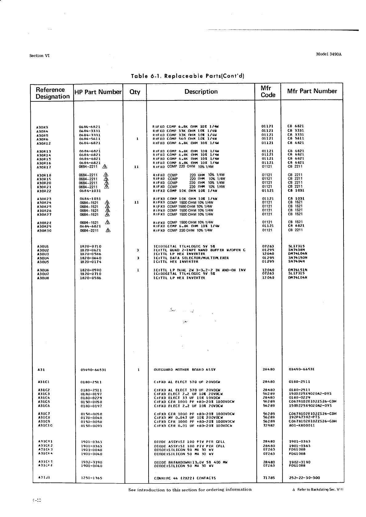
Section VI Model 3490A
Toble 6-1. Reploceoble
Ports(Cont'd)
Reference
Designation
HP Part
Number oty Description Mfr
Code Mfr Part
Number
A3OR3
A3OR4
430R5
A30F6
a30Rl
2
a30R I 3
a30Rl
4
a30Rl 5
a30Rl
6
a30R I
7
a30R I I
a30R
I
I
430R20
430R2
r
AaoF22
l30R
2
3
a30R2
4
aloR2 5
130R2
6
A3OR2
?
^30R2 t
130R29
A30R30
^30u1
430u2
A3OU3
Atot14
A3OU'
A30U6
430{r7
a30lr8
afl
13lcl
^ttc2
Ä3
lca
^3tc4
a3
lc5
13lc6
l3lc7
t3lc8
a3lc9
a3lct c
l3 ICR
I
13
lcß 2
r?
lcF
3
l3l cF
4
l3lcF:
r3
l;p 6
r_:lJl
0684-6n2 I
06
84-33i I
06a4-333t
0684-56r
I
0684-682 I
ooa+-oaz i
06a4-68? I
0684-6A2 I
06 84-682 I
684-2211
06'8/.,2211
ß44-2211
ß44-2211
068/,-2211
0684-lO3
t
0644-l o3
I
0684-1 521
068,r-1521
068/t- 1521
0684-1521
0684- 1521
o6a4-6421
0684-2211
1820-o?l o
1820-o62 t
l8 20-o 5a6
la2(F0640
1820-o174
t820-0590
t8 20-o7t o
I 820-0546
A.
A
/Ä
,A
l*
A
A
A
01490-66531
0t80-25t I
0 r80-251 I
ol ao-ot 97
ola0-o22 9
ot 50-o050
ol80-01e7
ol 50-o05 0
o
170-o040
ol 50-o050
ot 50-oo93
l90l-036f
l90l-0363
190
t-oo40
190 I-0040
19 02-
3
190
I 901
-O()4
O
l25l-1365
I
II
ll
7
t
I
I
R:FXD CO'{P 6.8K OHM l0l l/4tl
R:FXD COftP 33K OHl,t lot l/41
R:FXD COHP 33K fHl,r 101 ll4U
R:FXO COXP
560 oHN lot l/41
R:FXD COIIP 6.8K OHt{ lot l/41
R:FXD C.OilP 6.aK OHll l0l l/4x
R:FXD CONP 6.8K OHl.r tol l/41
R:FXO COIIP 6.AK OHf{ lot l/4rl
R:FXO COI|P 6.AK OHfi IOZ llt*l
R:Fxo COMP
220 OHM 10961/4W
R:FXO COMP
R:FXO coMP
R:FXD COMP
R:FXD COMP
R:FXD COIIP IOK
220
0H& 1096 1/4W
220
ot+, lM 1/4W
220 oHr lW" 1l4W
220 oHn 1trÄ 1/4W
olü lot t/tl
RIFXO COf{P IOK OHr lO? 1/4H
R:FXD COMP 1500OHM 10% 1/4W
R
iFxD COMP 1500 OHM 1096 1/4W
R:FXD COMP 1500oHM 10%1/4W
R:FXD COMP 1500 OHM 10% 1/4W
R:FXD coMP 1500oHM 10%
1/4W
R:FXD COXP 6.aK OH,l l0l l/41
R:FXD COMP 2200HM 1ü6114W
lC:oIGITAL TTL+LOGIC tV 5l
IC:TTL OUAD 2-II{PI NAI{O SUFFER I/OPEN C
IC:TTT fP HEX INVERTER
IC:TTL DATA SELECIOR/IiULTIOtEX€R
IC:TTL HEX INVERTER
IC:ITL LP DtlÄL 2r a-1.2-2 lN ANO-OR INv
IC:OIGITAL TTL+I.OGIC 5V 5I
IC:ITL LP HEX INVERTER
OI'TGIIARD IIOTHER SNARD ASSY
C:FXD AL ELFCT 370 UF zOVDCII
C:FXD AL EI.ECT 370 UF zOVDCT
C:FXD ELECT 2.2 UF lol 2OVm.B
C:FXD EI€CT 33 UF lol IOVDCH
c:Fxo cER looo PF +a0-201 looovocr
c:fxD EL€CI 2.2 UF lot 2oVDC|.
C:FXO CER lOr)O
PF +8G-2Ol IOOOVDCT
c:FxD l|Y 0.047 UF l0l zoovD(.ll
C:FlD CFR IOOO
PF +8O-2Ol IOOOVDCI{
C:FXD CER
O.0l UF
+8(F?Ol IOOVDCH
DIOD€
ASSY:SI IOO
PIV PFR
CELL
OIODE
ASSY:SI IOO PIV PER CFLL
oIooE:slt-lcot{ 50 l.a 30 Uv
oIoDE:SILICON
50 IA 30 tV
DIOD€ EREAXDOHN:L3.OV
51 400 l,lll
otooE:srLlcoN 50 La 30 Hv
coÄ,N:Pc 44 l?.x221 coNTAcTs
ol
t?l
ol l2l
ott2l
01 121
ol l2l
oll2l
oll2l
ol l2l
oll2l
01 121
01121
01121
01121
01 121
ol l2l
oll2l
01121
01121
01121
01121
o't121
olt2l
01121
ot263
ol 295
12040
ot29,
oL295
l2 0io
01 261
l2 040
2844O
28480
28480
562A9
28480
56249
562A9
56249
562
89
56249
729a2
za4ao
28480
o7
?61
or26l
2a4AO
o726)
7l 785
c8 6821
ca 3331
ca 3331
cB 56ll
ca 6821
cB 6821
cB 6821
cB 6821
c8 6821
cB 2211
cB 2211
cB 2211
cs 2211
ca 2211
ca lo31
c8 lo3l
cB 1521
cB 1521
cB 1521
cB 1521
cB 1521
c8 6821
cB 2211
sL l731 5
st{?438N
oil?4L04t{
sfi74150N
sN7{04N
olt74l51N
sL17315
Df{?4LO4N
0349G-66531
ot 80-25 I I
ol 80-25 I I
150D22
5 X902 0A2-DYS
ol ao-o2 29
co678102ElO2tS26-CDH
t 500 22 5 X 9020A2-DY
S
co67 8102
E
l02zs 26-coH
192P473
92-PT S
c067 Bl
o2 E
LO2 ZS26-COH
801-K8000 I I
l90l-o3 63
1901
-0363
FOGI
088
FOeloSa
t902-3 I 90
FDGI
088
252-22-)O-aOO
See introduction to this section for ordering information A Re{er to B&kddir€ Sec. Vrll
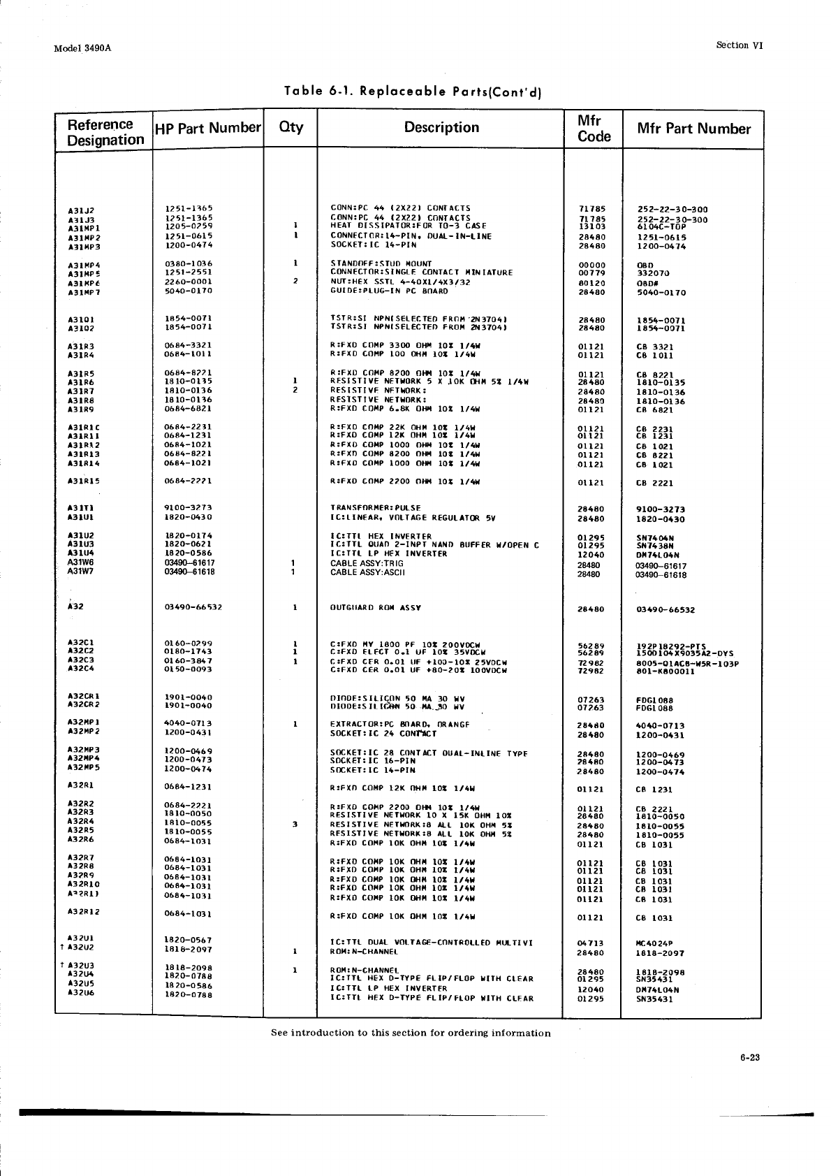
Model 3490,{ Section VI
Tqble 6-1. Reploceoble
Ports(Conr'd|
Reference
DesignationHP
Part
Number otv Description Mfr
Code Mfr Part
Number
^31J2
A3IJl
^3 lr{P
r
a3lt1P2
^atÄP3
^1lt4P 4
A3lllP
t
^all1P6
^3 lxp ?
a3lol
A3tO2
Ä:t
lR3
A3lR4
A3IR'
A3lR6
t3 lR7
A:] lR8
l3 lR9
13lRl c
l3lRl I
13lRl 2
r3lßt 3
t3lRr 4
13lRli
A3 trl
lalul
l3lu2
A3IU3
131rr4
A3rW6
431W7
^32
^32Cl
^t2c2
^?2C2
AtzC4
t32CR r
Aa2Cß.2
Ä32rP
I
,32,'? 2
a32XP3
^32,4P1
a?2tc5
A32RI
^32R2
l32R:l
A:I2R4
A3?R5
432R6
A3?R7
A3
2R8
l3?R9
^32RlO
A2?RI
I
A32rt2
3 2Ul
^42u2
At2u!
^3Z(l4
132U5
132u5
I
1
L25l-1765
t25l-Lt65
L205-o?5e
l2 5l-061
5
t200-o47 4
0380-l 036
L25t-2551
22t O-OOOI
5040-0
170
18
54-OO7
I
1854-OO7
I
0684-3221
0684-lOl I
o6b4-8?? L
l8 lo-0 t?5
l8 lo-o116
l8 lo-o I 36
0684-682 I
06a4-2211
06a4-l 23 I
0684-l O2
I
06a4-4221
0684-l02 |
o6a4-2221
9l 00-327?
1820-043
0
l8 20-o 174
1820-062 I
1.8 20-o 586
03490-616 17
03490-61618
ot490-665t2
ol 60-0299
o
I
80-l 741
ol 60-3a4 7
ol 50-o093
190
l-0040
190
l-oo40
4040-o7l 3
1200-043 I
1200-0469
1200-04t
3
1200-04?4
0684- t
23 I
o684-2221
la lo-0050
I
I I O-O055
l8
lo-0055
0684- I 03
I
0684-l 03
I
06E4-1
03
I
0684-l ot I
()684-l 03
I
0684- I 03
I
o6a4-t 03
I
1820-O56
7
l8l 8-2
097
l8 l8-2098
I 82
0- 07a8
l8 20-o 5a6
182
0-o7a8
t
I
?
I
1
I
I
2
I
I
I
I
I
t
I
CONN:PC 44 l2X22l C0NTACTS
coNN:PC 44 t2)/.22t CONTACTS
HEAT DISSIPATOR:FOR
TO-3 CÄSE
CONNFCTOR:
I4-PINr DUAL- IN-LINE
SOCKET:
lC l4-PlI
STANDOFF:STUD }IOUNT
CONNECTOR:S
IN6LE CONTACT }ITI{
IATUR€
NUT:HFX SST|_
4-4OXl/4X3l32
6UIDE:Pf U6-II{ PC BoARD
TSYR:Sl NPNI
SEIECTED FRolt .Ztil37o4l
TSrR:Sl NPNISEI-ECIED FRot a{3ZO4t
R:FXD CO'{P 3300 oHr lot t/{L
R:FXD COI{P lO0 oft}t lot l/4ta
R:FXD COilP 8?00 (}l+l
RESISTIV€ NETI'ORK 5
RESISTIVF NFTTORK:
RFSlSTTVE NETIIORK:
R:FXD CDf,tP 6.at( OHr|
57 tllU
Lt41
L l4U
ll4\l
I l4r
tt4ll
tt4ta
tl.*l
T RAN SFOR
I,IER: PULS
E
IC:IINEAR, VOLTAGE REGULAT(n 5V
IC:TTI HEX INVERIFß.
IC:TTL OI,AO 2-INPT NAI{D EIIFFFR x/oPEN
IC:TTT LP HEX tI{VERTFR
CABLE ASSY:TRIG
CABLE ASSY:ASCIl
OUTGIIARD ROT ASSY
c:FxD |tY 1800 PF lot 200vocr{
C:FXD Et.FCr o.l UF lol 35vDCt
c:FxD cFR O.0l uF +too-tot 2'vocr
c:FxD c€R o.ol uF laG-201 loovDcr{
DIODF:SILICNN 50 TA 30 TV
nIoDE:sIt tfh{{ 50 r ..j]o tav
EXTRACTOR:PC 8NARD. ORANGF
SOC|(ET:lC 24 CONfiCT
SOCXEI:IC 28 COillml OuAt-Il{LINE TypF
SOCKET: IC 16-PlN
socKET: tc l4-Pll{
R:FXD COI'P 12K OHil lol l.r{}l
R:FXD COIrP 2200 oHa lot l/4L
RESISTIVE NETI'ORX IO X 15T OHH IOI
RESISTIVE NET$)RK:8 ALL IOK OHX 5:
RFSISTIVE NETIIORI(:8 ALL IOK OHX 5I
R:FXD COüP IOK OHl4 tot l/atJ
R:FXD COIIP
R:FXO CO'IP
R:FXD COXP
R:FXD COIiIP
R:FXO COilP
22K otr lot
l2K OHI
lot
loo0 DHfi l0l
8200 olst lot
looo olH lol
I0t l/4r
x lox (}rr
lol l/4ra
tot l/41
lot l/4r
10: l/ir
loi 1/4r
R:FXO COttP 2200 ol{,t lot
R:FID COIIP lOK 'rt||l
R:FXD COIIP IOK OHll
R:FXD COl,lP IOK Ollll
R:FXO CO'IP IOK OHll
R:FXD COiP IOX tltl{
R:FXD COItP tOK OHil lot l/4r
I C:
Tll OUAI- vot.aAGE-C0NIRoLLED
r{rjlTI yt
ROK:
N{HAl{NEI
RO'{: N-CHANI{EI.
TC:TTI HEX
D-TYPE FLIP/FI.OP
r,IIH ctEAR
IC:TTL TP HEX
INVERTFR
IC:TTI HFX
D-TYPE FLIP/FtoP TITH
cLFAR
7L7A5
7l?85
13l03
28480
2A4AO
o0000
0o779
80120
?8480
28480
28480
olr2l
oll2t
oLl2l
28+aO
284 80
28440
otl2l
oll2l
otl2t
or
l2l
oll2l
ort2t
oll2r
?8480
?8480
01295
ot295
t2 040
2Uü
z8r',Ao
24480
562A9
562A9
129A2
7?9A2
07
263
o7 261
26+dO
z8{80
28480
?8 t80
2 8480
ol
l2l
oI l2l
28480
28460
2A4AO
oll2l
oll2l
0ll2l
ot l2l
oll2l
oll2r
or
l2l
04
713
28480
28480
ol 295
12040
01295
252-22-30-300
252-22-tO-tOO
6l o4c-ToP
I
251-06t 5
1200-0474
OBD
332070
oaD*
5040-ol 70
I 6 54-OO7
I
I 854-O07
I
c8 3321
c8 loll
c8 8221
l8 ro-ot 35
I I r0-ol 36
lalo-ol:15
c8 6821
cg ?ztl
c8 l23l
c8 lo2l
c8 8221
cB lo2l
ca 2221
9loo-3273
1820-ot30
sN740+l{
5lr7438rl
otT4LOtN
03490-6161
7
03490-61618
03{9(F56532
19
2P 18292-Pr S
r500 l(}4 x9035a2-oY s
8005-o lAcB-H5R
-l 03P
801-Kroool I
FDGI
OAA
FOGI
088
40{o-07 I 3
1200-ot3 I
1200-o469
l2 00-0473
1200-o47a
c8 1231
ca 2221
18 lO-OO5 0
l8 lo-0o55
I 8lO-OO55
c8 lo3l
c8
CB
ca
c8
CB
c8
I
O3l
1031
I O3l
l03t
I 031
l03l
xc4024P
t8 l8-209?
I 8l 8-209 I
sN3543
I
Dil74L04N
sN3543
I
See introduction to this section for ordering information
6-23
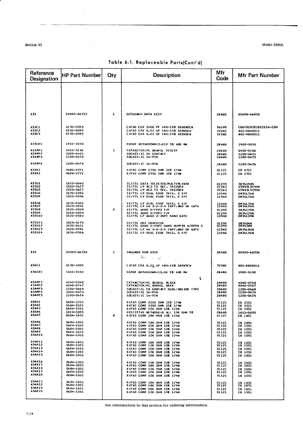
Section VI Model 3490A
Tqble
6-1. Reploceoble
Ports(Cont'd)
Reference
Designation
HP Part
Numbet oty Description Mfr
Code Mfr Part Number
^3t
a33Cl
^13C2
^?tc,
433C8 I
133LP
I
tlatlP 2
a33r{P3
^)IAP4
r33R
I
433R2
A33UI
^31U2
433U3
a33tr4
433U5
133U6
Ä3:tu7
Ä33U8
A33U9
l33Ul 0
A33U I I
Ä3tu12
a33Ul
3
t33Ul 4
^34
l34Cl
r34CR
I
l3{tP I
^344P
2
A3+tP3
^t4AP4
A:I4FP
5
A:t4RI
^14e2
134R3
134R4
A:t4R5
434ß6
434R7
434R8
A3{R9
aSaa
I c
A34F
I I
a3{R
I 2
af4Rl 3
A:]4R
l4
t3{Rl 5
A]{Rl6
l34R I 7
A:LRl I
r3aRl s
r34R20
^:'4F21
^tae22
^*a2z
a*e21
oa4.to-66534
01 50-0 05 0
ol 50-o093
ol 50-oo93
1902-303 0
0403-ol 86
t200-o43 r
120(F0473
I200-o4?4
o6a4-472 L
o6a4-27 2l
la2 0-0640
LA20-O627
la20-062 7
t8 20-o 596
Ia20-0596
18 20-o 596
LA20-O59l
16 20-o839
ta20-o83 9
ta 20-o 5a3
1820-ol 74
l8 20-062 I
la20-o59
I
l8 20-o 596
03490-66534
ol 50-0093
I902-3 190
4040-o748
4040-o747
l2 00-0469
L200-o473
1200-0474
o6a4-222L
0684-3 32 I
0684- I 53
I
l8 I
O-0O55
0684-1831
06 84-l 83
I
0684-I 03
I
0684-l03 I
068 4-
lO3 I
06a4-l 03l
()6a4-la3 I
o6a4-l 03 I
06 8+-lot I
0684- I 03
I
0684-I8 I I
06a4-l 03
I
06a+-1831
0684-t O3
I
{J684-
I
O3l
0684- I O:l
I
0684-18f1
o6a{-l 83
I
06a4-t83 I
068a- I 01
I
I
3
I
8
Lf4Y
ll 4r
I
t4l
It4u
l r4Y
OUTGT'ARO
DAIA ASSY
csFlD cER looo PF +a(F20f looovDct.
C:FXO
CFR
O.Ol UF +80-2Ot lOoVOCt{
c:FxD cFR O-Ol UF .a(F20t loovocl
Dloo€ aFEAKOOTN:3.OlY 5t 400
EXTRACTOR:PC EOAR{L VIOL€I
SOCKET:IC 24 CONTICT
5tr,K€T: I C I6_PIN
SOCKFT: IC l4-Pll{
R:FXO CoHP 47OO Ollr't lot l/41
R:FXD C0f{P 2700 oHt lO! t/41
IC: TT L OATA 5EL€C TOfi,/I'IULIIPL
EXER
If.:TTL f P BCO TO tEC. DECOof,R
IC:TTL t,P 8CD TO D€C. DECOD€R
IC;TTL LP DTIAL EOG€ TRIG. D f/F
IC:fTI LP DT'AL EOGE TT,IG. D F/F
IC:TTL IP DIIAL EDG€ TRIG. D F/F
lC:Trt LP 4l t-2-2-3 INPT.Ar|O Ofl, GATE
IC:TTL OIIAO D-IYP€ F/F
IC:TIL OUAO TFTYPE F/F
IC:TTL I.P OUAD 2-INPT IIAiIO GATE
IC:TTL HEX INVERTER
IC:TTL OUAD 2-INPI NANO ßIJFFER
I/OPEN C
fC:TTL Lp 4u a-2-2-a ltlPT.AriD OR G^TE
IC:TTL IP DTIAL
€OG€ TRIG. O F/F
INGUARD ROII ASSY
':
c:Fxo cEf{ o.o.L_uF +8(F2ol toovDc|.
DIOD€ ERF|KOOIiN:l3.OV 5: 400 f{l
EXIRACTOR:PC .OARO. .LACK
i
€XIRACTOR:PC BOIRO. GRAY
SMKFT:IC 2A COilTTCT DUAL-INLI}IE TYPE
socKET: tc 16-PtN
SmKEI: IC l4-PIta
R:FXD CO||P 220C OHfa l.O2 lt.t
R:FXO COIP 3300 otr{ lot l/4r
RIFXD COxP r5( OHtt lot l/4r
RESISTIVE N€f}tORK:6 ILI IO( OHII 5I
R:FXD COIiP l8r ülX lot l/41
R:FXD
COXP l8K OHtl
lot
R:FXD
COXP IOK (}tt 10t
R:FXD
COr,rP
IOK OHr( 10t
R:FXO
COHP lO|( OHt lot
R:FXD
CO,{P IOX OHt{ lO3
R:FXO
COIIP
l8X OHt lO: l/4ta
R:FXD
COIP 10( 0Hli l0l I/4L
R:FXD
COIIP lox OHlt
l0l l/4x
R:FX0 COIIP
lo( OHt. lot l/4r
R:FXD
COXP
l8K Ofrt 10t l/4I
R:FXD
CO|{P rOK OHt lot l/41
R:FXO COXP
l8K t)}ilt lot l/al{
R:FXD
COi{P lor OH||
LOt l/41
R:FXO
COriP IOK OHt lot l/(r
R:FXO
COXP lO(' OHr lot l/tr
R:FXD CO,{P
l8K ot{t{ tota tl4l
R.:FXD
CoxP l8R OHI lol l/41
R:FXO
CO'|P
l8K (ttl LOt Ll4l
R:FXO COrP IOK OHt tot l/4t
2Aaao
56289
72942
72942
28480
284 80
2a480
28+aO
284aO
oll2l
0lt2l
01295
o7 26?
07261
120
40
l2 040
120 40
l2 040
o1 295
ol ?95
1204{)
olz 95
01295
12040
12040
28480
729A2
2A4AO
2a480
28480
28480
28480
28480
otl2l
ol
l2r
oll2l
28480
0l
l2r
0l r2l
oll2l
oll2l
oll2l
or
l2l
0lt2t
ol
r2l
oll2l
otl2l
olt2l
ol l2l.
ol l2l
otl2l
ol
Izl
oll2l
o1121
01 t2l
otl2l
ol
l2l
I 831
I 031
1031
I O3l
lo:rl
I 8rl
l03l
I 03l
l03l
I Itl
loSl
l83l
l03 I
I03t
1 031
I
831
l83l
l83t
I
03l
oa49(F66533
co67 Blo2Elo2zs26-cDH
801-x80001
L
80 l-(8000 ll
1902-3030
0403-olE6
1200-ot3 I
1200-ot?3
1200-ot?4
ca +721
cb 2721
sN?4150N
u7893L0t 59X
U?893LOI59I
Dl{?4L7{N
Dt'{74L7+N
of,r74l-74N
Dfl7{t5{N
sr{74
t75N
sil?4l7ttl
Dn?rLoox
sta7404N
sN743ar
ol{TaLttN
Df{?tLTalt
03490-66534
aol-(aoo0 I I
1902-3t90
4040-0748
4040-o?47
12()0-ot69
1200-ot73
t200-ot74
ca 222L
ca 3321
cB 1531
l8 lo-oo55
ca l83l
c8
c8
c8
CB
c8
ca
CB
c8
c6
c8
c8
c8
ca
c8
ca
CB
CB
c8
c8
:-21
See introduction to this section for ordering information
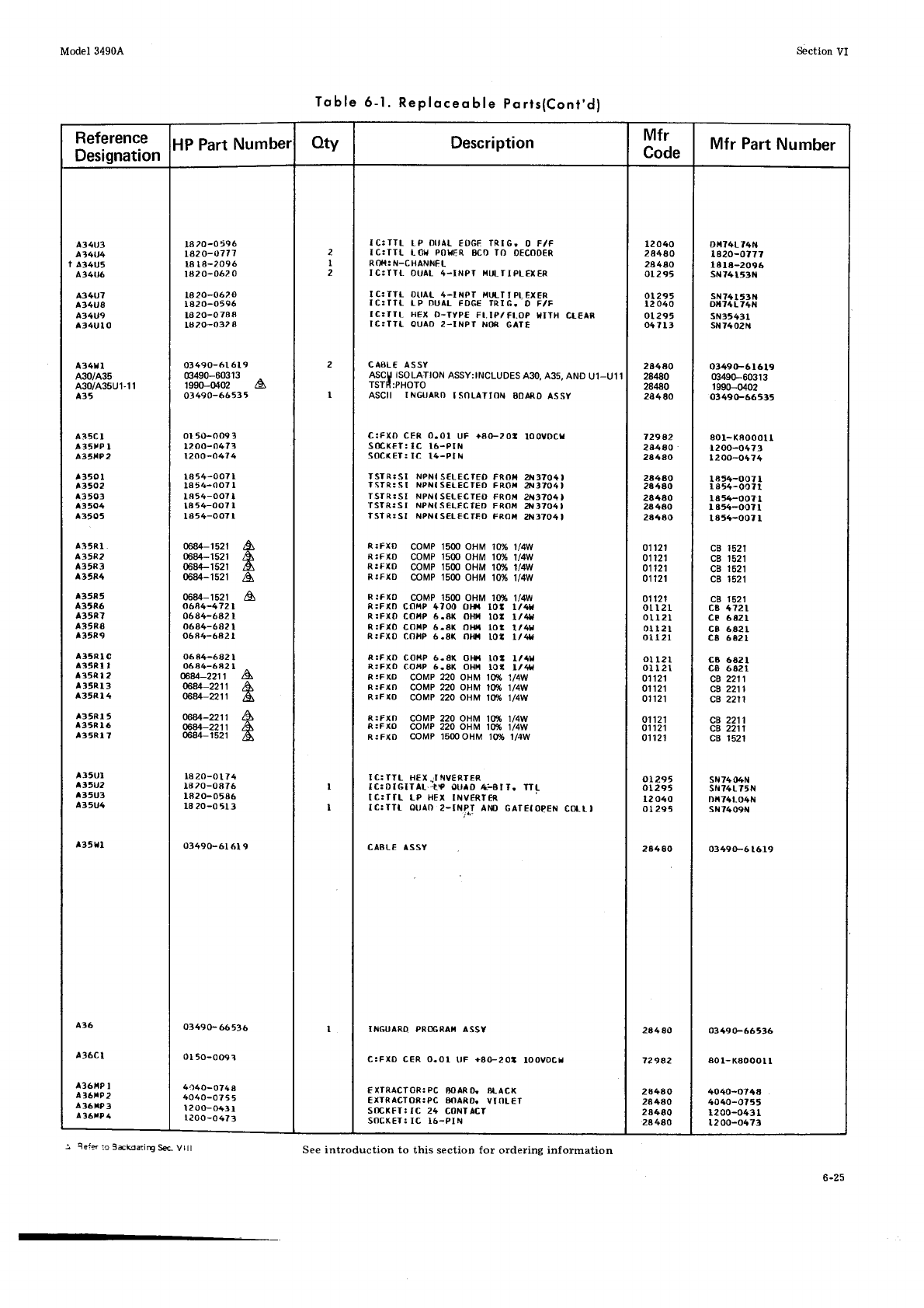
Toble
6-1.
Reploceoble
Ports(Cont'd)
Reference
Designation
HP Part
Numbet otv Description Mfr
Code Mfr Part
Number
434U3
A'4U+
I A)4ü5
434U6
^34U7
A34U8
434U9
A34U
I
O
A34Y
I
430/435
A30/A35U1.1
1
a15
a35C I
a35fP I
At5t1P2
rt50t
4t502
13501
^3504
43505
a35RL.
a?5e2
435R3
^35R4
r35R5
a3tß6
A3'R7
A39RA
135R9
a35RlC
a35Rl
t
A15Rl 2
t35Rt
3
a35Rl4
A35Rl 5
l35R
I 6
l35Rl 7
A35Ur
^t5u2
^35U3
135U4
l35Ul
436
a36C
I
^36t{P I
^16ttP 2
a36rP3
a36rP4
t8 20
-o 596
LA20-0777
1.8 t8-2096
la20-062
0
la20-o620
I 820-O596
t8
20-o 7aa
LA20-032 A
03490-61 6l 9
ß490-60313
1990-0402
03490-6653 5Ä.
0r 50-oo9 l
1200-0473
1200-o47
4
l8
54-007
t
1854-007
I
I
854-O07
I
la54-oo7
I
I
854-O07 I
0684-1521
0684-152
1
ffi8't-1521
0684-1521
0684- 1
521
o6a4-4721
0684-6a2 t
o6a4-682
I
06a4-682 I
o684-6a2 I
06a4-682 I
clj84-221'l
06,8r',-2211
068r',-2211
@€r'.-221r
06,8/-2211
0684- 1521
18
20-O
1 74
l8
20-o876
1820-058ö
l8 20-O 51
3
A
A,
A
A
A
A
,A
l$
A
4
0349(F616I 9
0349(F
66536
0
I 50-009 ?
4140-o74 I
{o40-0? 5 5
1200-o+31
r200-o6?
3
I
2
2
I
I
I
I
IC:TTL LP OI,AL EOGF TRIG, O F/F
IC:TTL LOI. POIER 8CD TO OECODER
R{}{: N-CHANNFI
IC:TTL DUAL 4-INPI III.,LIIPLEXER
I C: TTf DtlAl- 4-I lrlPT i,ltLT t pL
EXER
IC:TII IP DUAL FOGE
TRIG. D F/F
IC:TTI- HEX D-TYPE FI,IPlFI.oP TITH CLEAR
IC:TIL OUAO 2-INPT NOR GATE
CABLE ASSY
ASC$ ISOLATION ASSY:INCLUDES A30, A35, AND U1-U1 1
TSTR:PHOTO
ASCII INGTJARD
ISOLATION sOARD ASSY
C:FXo CER 0.Ol UF +8G-20t lOoVDCI
SOCKEI: TC I6-PIN
SOC|(ET:
IC 14-PlN
TSTR:Sl NPNIS€LECTEO FRot 2il37041
TSTR:Sl NPNIS€LECIED FROI{ 2fi3?O4l
TSrR:Sl NPt{l SELECTED FROtit
2N37O4l
TSIR:Sl NPN( S€LF.Cf€D FROr,t
r{37041
TSTR:Sl NPNIS€l-FCTFD FROil 2N3704l
R:FXD COMP 1500 OHM 10% 1/4W
R:FXD COMP 15@
OHM 10%
l/4W
R:FXD COMP 15m OHM
10% 1/4W
R:FXD COMP 15m OHM 10%
l/4W
R:FXO COMP 1500
oHM 10%
1/4!t/
R:FXD Ctll.rP 47OO Olfl 10t l/41
R:FXO COI|P 5.aX OHt,l lot l/4t
R:FXO
COI4P 6.ax OHH 10! l/4r
RIFXO COI{P
6.8K O}01
IOZ ltr*a
R:FXD
COftP 6.8K Oltt lot l/4r
R:FXD
CO|P 6.8X OHH t1t |ttü
RIFXD COMP 220 oHM 1096
1/4W
R:FXD COMP 220 oHM 1096 1/4W
R:FXD COMP 220 oHM 1096 1/4W
R:FXD COMP 220 oHM 1& 1/4W
R:FXO COMP 220 oHM 1096 1/4W
R:FXD coMP lsmOHM l@tD 1l4W
IC:TTL HEX:INVEI,TER
IC:DIGtT^L."t]9 ottaD 4:8tr. TTL
IC:TfL LP HEX
INVERTER
lcrrTL OUAD
z-INPT ÄiD cATEtOeEil
Cot-Lt
caELE lsst
INGUARD PROGRAI,,I ASSY
clFxD cER O.Ol t'F +8(F201 loovocl
EXTRACTOR:PC
80ARO, ELACK
EXTRACTOR:PC EOARDT
VIOL€I
SmKFT: IC 24 CONTICT
SOCK€f: lC l6-PI N
12040
2A4AO
2S4AO
01295
01295
l2 040
ol 295
04
713
2A4AO
28480
28,180
24480
729 A7-
28480
28480
2A4AO
28480
28480
28480
24480
01121
01121
o1121
01121
01121
otl21
otl2l
0lt2l
olt2l
olt2l
oll2l
01121
01121
01121
01121
01121
01121
ol.295
o1295
l2 040
ot295
28480
2E4
80
72942
28480
24480
28480
24480
Dil74L74N
1820-0777
I 818-2096
sN74l53N
sN74L53N
Dt{74L74t{
sN3543l
sN7402N
0349(F6l619
@490-60313
1990-0402
03490-66535
801-
K8000ll
1200-0471
1200-o{?4
1854-OO7l
I 854-00?l
1854-OO?
I
I 854-OO7l
I 854-OO7
I
CB
CB
CB
CB
c8
cs
c8
ca
c8
.A
.A
CB
1521
1521
1521
1521
1521
1721
6821
6A2t
6A2l
6A2
I
6821
2211
2211
2211
2211
2211
1521
SN
74 O/oN
sN74L 75N
DftTtL04N
sN?409N
0349(F6 t6l9
03490-66t36
801-K8000tt
4040-o?48
4040-o?55
1200-043 I
1200-0471
Model
34904 Section VI
j qeJs :c g4kcair€ Se Vil l See introduction to this section for ordering information
6-25
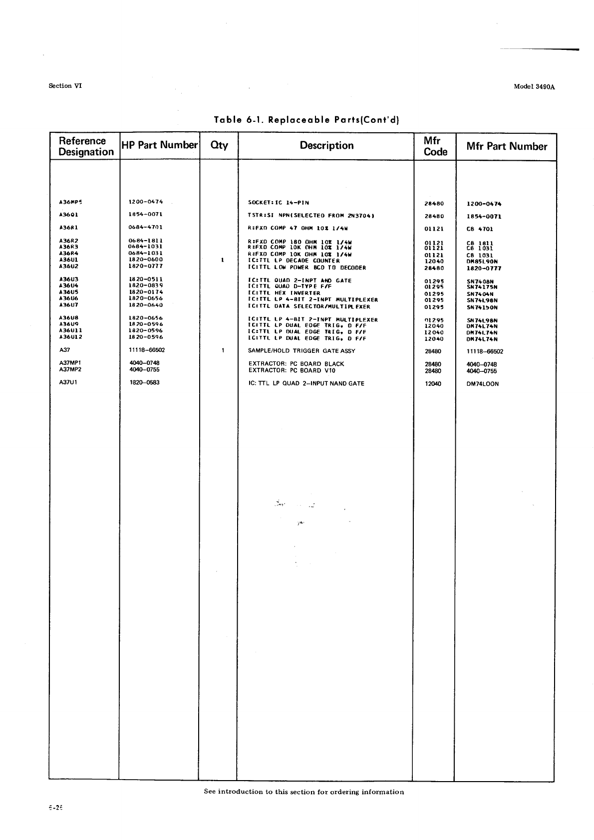
Section YI Model 3490A
Toble 6-1. Reploceoble Po
rts(Cont'd)
Reference
Designation
HP Part
Numbel otv Description Mfr
Code Mfr Part Number
^?6r{P.-
Ä3601
l36Rl
436R2
436R3
436R4
A36UI
At6U2
t36U3
A36U'
A36U'
436U6
436U7
Ä36U4
436U9
a36Ul I
^36Ut2
A37
A37MP1
A37MP2
A37U1
t200-o474
1854-O07l
o6a4-4701
06 84-l Al I
0684- I O3 I
o6a4- I 03
I
l8 20-o600
t 82 0-o77 7
1820-o5l
I
I 820-O83 9
t820-or?4
182 0-o656
La20-o640
t82 0-o656
1820-o596
la20-o596
1820-0596
1 1 1 18-66502
4040-0748
4040-0755
1820-0583
I
SOCXET:
lC l4-PlN
TSTR:SI NPNISELECTEO
FRor. ä{3?041
R:FXD
CO|{P 47 oHt lot l/4ta
R:FXD
COttP 180 oHx lot l./4r
R:FXO
COtlP loK OHfl
lO! l/4r
R:FXD
COSP
IOK OHä lol l/41
IC:TTI LP OECAD€ COUN'€R
IC:TTL LO|, POIIER
8CD TO DECOO€R
IC:TTI. OUAO 2-INPT AID GATE
IC:TTL OUAD
D-TYPE F/F
IC:TTL HEX
INVERTER
IC:TTL LP 4-8IT 2-INPT |IULTIPLEXER
IC: fTL DATA
SELECTOR/IUI.TIPt
EXER
IC:TTL LP 4-BIT 2.IT{PT I{UI,TIPLEXER
IC:TTI IP OUAL
EDGF TRIG. O F/F
IC:TTI LP IX,AI-
EOG€ TRIG, D F/F
IC:TTL LP DUAI,
EDG€ TR,IG. D F/F
SAMPLE/HOLD
TRIGGER GATE ASSY
EXTRACTOR:
PC
BOARD
BLACK
EXTRACTOR:
PC
BOARD V10
lC:
TTL LP OUAD
2-INPUT NAND GATE
28480
2a4AO
ol l2l
ol 121
oll2l
ol l2l
lao40
2A480
01295
0t295
ot295
ot 295
ot295
ot29t
12040
12040
12040
2&AO
28480
28480
t20/o
lzoo-o47+
r854-OO?l
cB 4701
c8 l.8ll
c8 Lo3l
ca 1031
Dfr85L90||
ta20-of7.7
sN74oAN
slr?41751{
slt7404r{
sN74L9aN
sfl74150N
sN74L9Ail
DX74L74N
Dfr74L?4r.1
Dfrt+L74N
'| 1 1 18-66502
(wJ47ß
4040-0755
DMT4LOON
See introduction to this section for ordering information
a-24
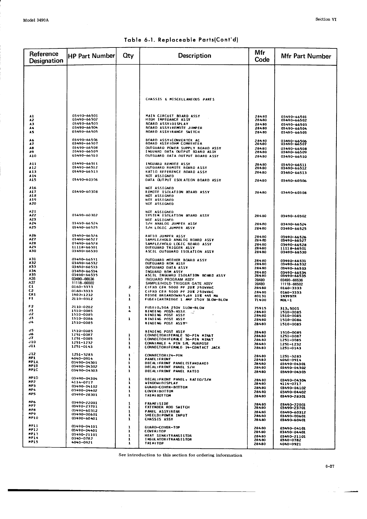
Reference
Designation HP Part
Number oty Description Mfr
Code Mfr Part
Number
AI
A2
A3
A4
A'
A6
l?
AA
A9
^lo
A2l
^22
^21
A21
^25
A26
A27
^24
429
430
F2
JI
J2
J3
J4
J5
J6
J?
Jlo
Jll
all
^t2
al3
at4
al5
Ä16
al7
al8
al9
^20
a3l
432
a)
a3r
435
436
A37
cl
c2
cRl
FI
J12
fiPl
ilPIA
XP
IB
riPlC
I,IP
ID
tP2
tP:l
üP4
,4P5
t1P6
,4Pl
tPa
raP9
xPlo
,IPI I
TPI2
rPI3
iP l4
xPl 5
034S(F66501
03490-66 502
0349
0-66503
01490-66504
o349
0-66 505
o349{F66506
03490-6650?
03490-6650a
03490-66509
o3490-665t O
03490-6651 I
03490-66 5l 2
0349(F66 513
01490-603 06
of490-6030a
o1490-60 302
ot490-66524
0349(F66525
Oat 9O-6652 6
oSt.9o-(a527
or490-665? A
ll I l8-66501
03490- 66530
0349(F66531
0749(}-66532
03490-66533
03490-66534
03490-6653 5
03490-66536
1 1 1
t8-66502
ol 60-r33 3
ol 60-333 3
t90 2-t2J2
2l lo-o3t2
2tto-o202
I 5 I O-OOA5
l5 I O-OOA5
l5 I O-OOa6
15 lo-oo8 5
I5 I O-008
5
l2 5l-o087
125t-O085
t25
l-l ?12
l25l -o143
L25l-a283
4040-0914
03490-043{) I
03490-04302
03{9(F04303
0349(F04304
4l I4-O717
0349(F04lO2
o!490-04402
0349(F28301
03490-22001
03490-2370 r
03490-60312
()3490-OO60t
03490-60 40
I
0349
0-O4
lO I
o1490-04401
03{90-2 I lO I
o3+o-o?6 2
40{o-o92 I
2
I
I
I
t
I
I
I
I
I
I
I
I
I
I
I
I
I
I
I
I
I
I
I
I
I
I
I
CHASSIS 6 IIISCELLANECI'S PIRTS
I.iAIM CIRCUIT ENARD ÄSSY
HIGH I'.IPEOANCE
ASSY
BOARD ASSY:OISPLAY
BOARD ASSY;REI{II€ JT'T|PER
AOARO ASSY:RÄIGF s|ITCH
BNARD ASSY:COIIIY€RTER
AC
BOARD ASSY:OHI{ COTWERTER
OUTGUARO POIER SUPPLY EOARD ASSY
I'{;UARD DATA d'TPUT BOARO ASSY
OUTGUARO DATA OUTPI'T BOARD ASSY
INGUARD REf{OIE ASSY
UUTGI.,ARO
REAI]TE SOARD ASSY
RATIO R.EFERENCE
BOARD
ASSY
NOT ASSIGNED
DATA O,'|TR'T ISOI.ATION SOARD ASSY
NOT ASSIGNEO
REMOTF ISOTATION
NOT ASSI
GNED
NOT ASSIGN€D
NOT ASSIGNED
EOARD ISSY
NOT ASSIGNED
SYSIEII ISOLATIOI ENARD ASSY
N(JT ASS
IGNEf)
S/H ANALOG JI'I'P€R ASSY
S/H LOGIC JUHPFR ASSY
AATIO JUI.IPFR ASSY
SAIlPI.E/HOLD ANALOG
BOARO ASSY
SAI4PL€/HOLD Lff;IC BOARD ASSY
OI'TGUARD TRI6G€R ASSY
ASCIL OUIGUARD ISOI-ATION ASSY
NUTGUARD I.IOIIIER BOARD ASSY
OUTGUARD ROT ASSY
OUIGUARD DATA ASSY
II'IGUARD ROr ASSY
ASCIL INA'ARD ISOLATION OOAID ÄSSY
INGUARD PROGRAM ASSY
SAMPLE/HOLD TRIGGER GATE ASSY
c:FxD cER 5000 PF 20t 250I,YAC
C:FXO CER 5OOO
PF 20: 25ory C
DlOa)€ BREAXDOBI:5.6V tol 445 ta^
F1AE:CARTRIDGE I ltip 250V g-Or-8LOl
FtrsE:o.5oA ?50v SLot-BLOr
BINDTa{G Pot},assy. _--
EINOI'S POST ASSY
EIlrDtrs PosT. assY
BINDTT{G POSI SSI'
BTiIDING POST ASSY
CONNFCTOR:FEIIAL€ 5O-PIN I{INAT
CONNECTOR:F€IiIE 36-PIX XINAT
CONII:IIALE 4 PIN SPI. RJRPOSE
CoNNECTOR:F€HILE. lt-g)atTlcT J Cr(
CONNECTOR:24-PI
N
PANEL: F RON'
DECAL
:FROilT PAilEL (SIAI{OARD)
D€CAI.:FRONI PANEI- S/H
O€CAL:FRTI}IT PAII€T RATIO
DECAI:FRONT PANEL. R.AIIO./S,'H
HIIooH: DISPLAY
GUARH OVER-AOTTOI{
C(|vER
: BOTTOI
TRIII: BOTTOX
FRAIIF:SIDE
EXTFNDER ROO ST'IICH
PANEI- ASSY:REÄR
SHIELD: POI€R IiIPUT
cx^ssIs assY
GUARTHOVER-TOP
C OVE R,: TOP
HEAT SINKsTRAilSISTOR
I nsul AroR,:TRAti6 I SrOR
T
RI T: TOP
284 80
28480
28480
28{80
28480
284 80
28480
284E0
28480
2A480
2a480
28480
284aO
28480
za4ao
28480
24480
28480
28480
284 80
284 EO
28440
2A480
28+80
24t80
26460
28480
2a+ao
28480
28/l80
28t80
2atao
8013t
Tlioo
759 15
2A4aO
28480
28480
2S4AO
284r0
2a+ao
2A480
28480
28480
2g4AO
284aO
2E4AO
28480
28480
28480
28480
28480
28{80
2448(}
28480
28480
28{8d
2A480
28480
28480
284aO
28480
24480
28t80
0349{F66501
o3190-665o.2
ot490-665oiJ
('3490-6650+
0349(F66505
03490-66506
03490-66507
03+9G-66508
03a9(F6650!)
0349(F665lO
03490-665 ll
0349r66512
03490-66513
0349(F603(}6
0349160t08
0349(F60a02
o34e(F6652t
0349(F66525
0349(F66526
03{9(F6652?
0349(F66528
I I ll 8-66501
oa49(F66530
0349r66531
ot19t665t2
03t9(F66533
03190-665:ra
o:!190-66535
03490-66536
1 1 1 18-66502
ol6(F3333
ol60-3333
llr:r99?R
IDI_-I
3l 3. 500s
I5 lO-OOa5
l5l(Foo85
l5l{Foo16
I 5 tO-OOA5
I 5 IO-OO85
l25l-008?
t 2tl-o065
L25t-t2r2
l25l-o 143
l25l-32a3
{o40-o9l{
03+90-o1301
o3a9(FOt!t02
0349(FO+t03
0349(FO430a
4lt4{71?
0349(FO{.102
03490-o+a02
ot49(F2At0l
0t490-22001
03{9(F23701
ot49(F60312
03+9F0060l
0:1a90-60tol
o3r9FO+lOl
0349rOaaol
o3{90-2 I lOl
o340-o782
+oto-o921
Model 34904 Section VI
Toble 6-1. Reploceqble
Ports(Cont'd)
6-27
See introduction to this section for ordering information
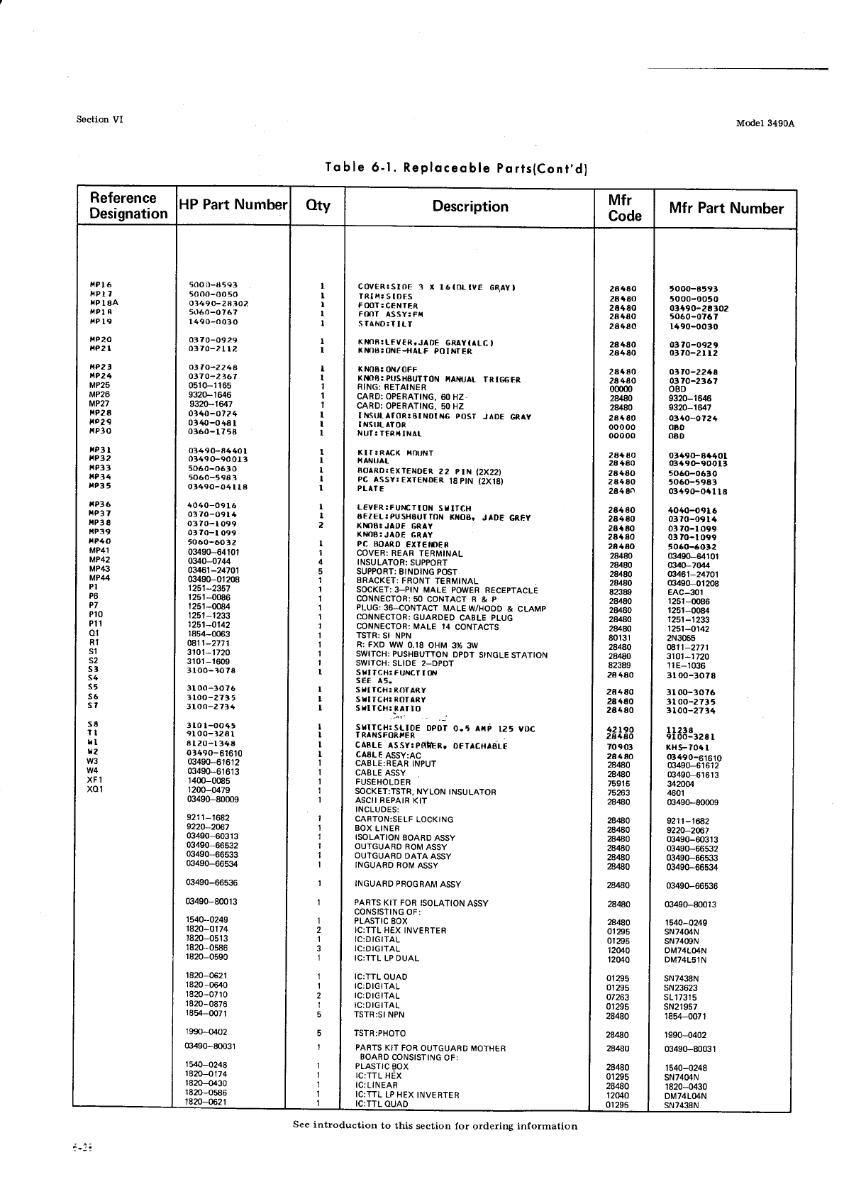
Seetion VI Model 3490A
Toble
6-1. Reploceoble
Ports(Cont'd)
Reference
Designation HP Part Number otv Description Mfr
Code Mfr Part
Number
fiPl6
tlPl
z
fiP
lAA
f,rPl8
r{P
l9
ilP20
AP2I
t1P2.3
AP24
MP25
MP26
MP27
ÄP2A
Ae29
r{
P30
fip3l
AP12
AP33
te34
tt?35
tP36
AP17
r{P3
8
iP39
tP40
MP41
MP42
MP4i}
MP44
P1
P6
P7
P10
P11
o1
R1
sl
s2
s3
s4
s5
s6
s7
sa
TI
tl
t2
w3
w4
XFl
xo1
500
0-8 593
5000-oo
50
o3490-28 302
5060-o767
1490-O03
0
03 70-09 29
o3fo-2 | | 2
otlo-224a
o!70-?_767
051 0-1 1 65
9320-1646
9320-1647
o740-o72 4
ot40-o4a I
0360- t7 5A
03490-84 40 I
0349
0-90 0t 3
5060-0630
5060-59A
3
o:t490-o4 lI 8
4040-o9l 6
03
70-09 l4
03
70- I
099
0370-l 099
5060-603 2
03490-64101
o340-o744
03461-24701
03490-012m
1251-2357
1 251
-0086
1251
-0084
1251
-1233
1251-O142
r854-0063
oal1-2771
3101-1720
3'r01-1609
3 loo- 3078
3t oo-fo ?6
?LOO-27t5
3too-2774
3 lo 1-oo
45
9l
oo-328
L
I I 20-l 348
o34eo-616
10
03490-61612
03490-6161
3
14m-0085
1200-0479
03490-80009
9211-1682
9220-20ß'7
03490-60313
03490-66532
03490-66533
03490-66534
03490-66536
03490-80013
1540-0249
1420-0174
1820-0513
1820-0586
r820-0590
1820-0621
1820-0erc
18m-0710
18m-0876
1854-007
1
1990-4402
8490-80031
1
54t!-0248
I
820-0 174
r82G-O430
1820-0586
1820-062 1
I
I
I
I
I
I
I
I
I
I
1
1
I
I
I
I
I
I
I
I
I
I
,|
I
I
1
I
I
1
1
1
1
I
I
1
i
I
1
I
I
I
I
I
I
1
I
2
I
I
4
1
1
1
I
I
1
I
I
1
1
1
,|
I
1
1
I
1
COV€R:SIDE 3 X l6tot-tVE GRAYI
TRII{:SIDES
F
OOT: CF'{TER
For|T ASSY:F{
STAND:T
ILT
KMlA:LFV€RTJADE 6RAYIALc I
Xt{fIB:ONE-fiALF POINIER
K NoA: ON/OFF
KMTB: PI'SHBUTTON üAilUAL TRIG6FN,
RING:
RETAINER
CARD: OPERATING,
60 HZ.
CARD:
OPERATING,
50 HZ
r ISUTATOR:EINOING POSI JADE
I NSI'L AT
OR
NUT:
TERITINAT
KIT:RACK XOI,NT
'1ANt'AL
AOARD:€XTENDER
22 PIN {2X221
PC ASSY: EXTENDER
18 PIN (2X.I8)
PLAT
E
LEV€R:FUISTTON SIITCH
AEZEL:PUSHEUTTON KIIOEI JADF GREY
KI{IO:
JAOE GRAY
KM}8!JADE
GRAY
PC EOARO
EXIC['{)ER
COVER:
REAR
TERMINAL
INSULATOR:
SUPPORT
SUPPORT:
ElNDlNG POST
ERACKET:
FRONT
TERMINAL
SOCKET:
3-PtN MALE POWER
ReCepfnCli
CONNECTOR:50
CONTACT R & P
PLUG:
36-CONTACT
MALE
WHOOD
& CLAMP
CONNECTOB:
GUARDED
CABLE
PLUG
CONNECTOR:
MALE 14 CONTACTS
TSTR:
SI NPN
R: FXD WW 0.18
OHM 3% 3W
SWITCH: PUSHBUTTON
DPDT
STNGLE
STATTON
SWITCH:
SLIDE 2-DPDT
s tl rcH: FUNCT
l(},l
SEE
A'.
SI,I TCH:
ROTARY
SIITCH:ROTARY
S
PI
TCH:TAT
I O -i
srITcH:sLtD€ opor o.i tti tz: voc
f RAr{sFORf.FR
CABLE
ASSY:POFER,
DETÄCHAELf
CAsL€
ASSY:AC
CABLE:REAR
INPUT
CABLE ASSY
FUSEHOLD
E R
SOCKET:TSTR.
NYLON
INSULATOR
ASCII REPAIR
KIT
INCLUDES:
CARTON:SELF
LOCKING
BOX
LINER
ISOLATION
BOARD
ASSY
OUTGUARO
ROM
ASSY
OUTGUARO
DATA
ASSY
INGUARD
ROM
ASSY
INGUARD PROGRAM
ASSY
PARTS
KIT FOR
ISOLATION
ASSY
CONSISTING
OF:
PLASTIC
BOX
IC:TTL
HEX INVERTER
lC:D
IGITAL
lC:DIGITAL
IC:TTL
LP DUAL
lC:TTL
OUAD
lC:DIGITAL
lC:DlG
ITAL
lC:DIGITAL
TSTR:SI
NPN
TSTR:PHOTO
PARTS
KIT FOR
OUTGUAFD
MOTHER
BOARD
CONSISTING
OF:
PLASTIC
BOX
lC:TTL
HEX
lC;LINEAR
IC:TTL
LP HEX
INVERTER
lC:TTL
OUAD
2A{80
28480
20480
28480
28480
2844O
2A4AO
284 80
2A4AO
00000
2A4gJ
28r',a0
28{ 80
ooooo
ooooo
2a+80
28
440
2a480
2A4SO
2A4AA
28480
2a480
28a80
28{
80
20480
28480
28{'AO
28r'.ffi
28480
823@
2A4AO
28/,80
28.180
28/,eo
80131
28480
2AßO
82389
28
480
2A480
28480
244.80
42t90
284a0
70903
28480
28480
28,|80
75263
28480
28480
28480
28480
2AßO
28480
24480
28,180
28€0
2A4AO
01295
01295
120/.O
12MO
01295
01295
07263
01295
28480
244€0
28480
24480
01 295
28480
12040
01295
I
5000-8593
5000-o050
03t9(F26302
5060-0767
1490-o030
0370-o929
ot70-2tt2
o370-22/t8
0370-2t67
OBD
9320-1
646
9320-1647
ot+o-o724
OBD
{]80
ot+9(F8'1401
(849(F90013
5060-0630
5060-5943
0349(F041l8
4040-o916
03?o-o9la
03?o-1o99
o3
70-l 099
5060-6032
03490-64101
0340-7044
ß461-24101
03490-01208
EAC-301
r251-@86
1251-0084
1251-1233
1251-0142
2N3055
@11-2771
3101-1720
1 1 E-1036
3 I OO-3078
3t oG-3076
3l oo-2
735
3
lo0-2734
I
1238
9loo-328 t
xH
s-70r I
03490-61
610
03490-61612
03490-6161
3
3420M
.1601
03490-80009
9211-16a2
9220-206.7
03490-@313
03490-66532
03490-66533
03490-66534
03490-66536
03490-80013
1540-0249
sN7404N
sN7409N
DM74L04N
DM74L51
N
sN7438N
sN23623
sL1731
5
sN21957
'1854-0071
1990-0402
03490-80031
1540-0248
sN7404N
1820-0430
DM74L04N
sN7438N
See introduction to this section for ordering information
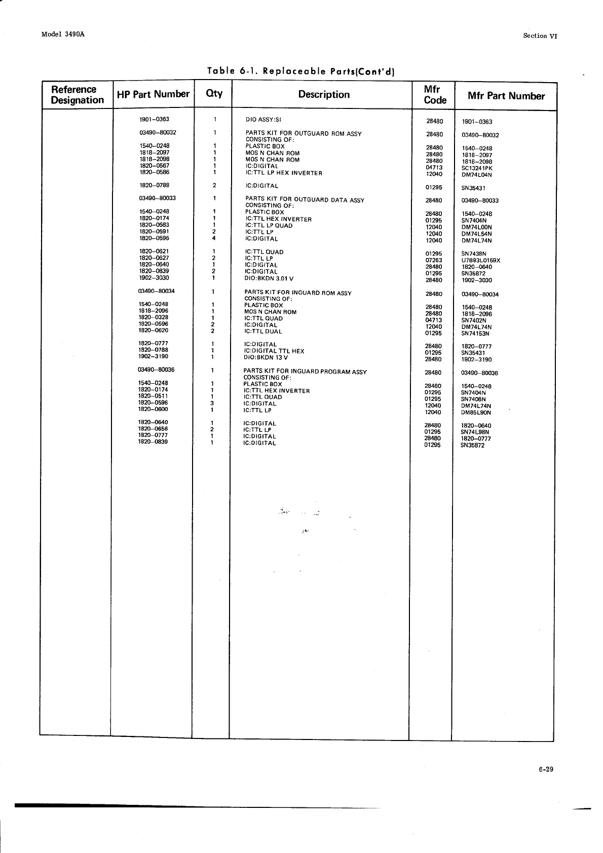
Model 34904 Section VI
Toble
6-l. Reploceoble
PortslCont'dl
Reference
Designation HP
Part
Number otv Description Mfr
Code Mfr Part
Number
1901
-0363
03490-80032
1540-O248
1814-2097
18
18-2098
1820-0567
1820-0586
1820-0788
03490-80033
1540-0248
1820-0174
1820-0583
1820-0591
1820-0596
1420-0621
1420-0627
1820-0640
1820-0839
r902-3030
03490-8@34
't540-0248
1818-2096
1820-0328
1820-0596
1820-0620
1420-0771
1820-0788
1902-3r90
03490-80036
1540-0248
1820-0174
1820-051 1
1820-0596
1820-0600
1820-0640
1820-0656
1Am-O177
1820-0839
1
1
I
I
1
1
1
I
1
4
'I
1
I
1
I
1
1
I
I
I
1
I
I
1
2
1
1
DIO
ASSY:Sl
PARTS
KIT FOR
OUTGUARD
ROM
ASSY
CONSISTING
OF:
PLASTIC
BOX
MOS
N CHAN ROM
MOS
N CHAN ROM
lC: D lG
ITAL
IC;TTL
LP HEX
TNVERTER
lC:DlG
ITAL
PARTS
KIT FOR
OUTGUARD
DATA
ASSY
CONSISTING
OF:
PLASTIC
BOX
IC:TTL
HEX
INVERTER
lC:TTL
LP OUAD
IC:TTL
LP
lC:DIGITAL
lC:TTL
OUAD
IC:TTL
LP
lC:DIGITAL
lC:DIGITAL
DIO:BKDN
3.01
V
PARTS
KIT.FOR
INGUARD
ROM
ASSY
CONSISTING
OF:
PLASTIC
BOX
MOS
N
CHAN ROM
lC:TTL
OUAD
lC:DlclTAL
lC:TTL
DUAL
lC:OIGITAL
lC:DIGITAL
TTL
HEX
DIO:BKDN
13
V
PARTS
KIT FOR
INGUARD
PROGRAM
ASSY
CONSISTING
OF:
PLASTIC
BOX
IC:TTL
HEX INVERTER
lC:TTL
OUAD
lC;DIGITAL
lC:TTL
LP
lC:DIGITAL
IC;TTL
LP
lC:DIGITAL
lC:DIGITAL
28480
28480
24480
28ßO
2a4AO
o4713
1204;0
0't295
28480
28la0
01295
12040
1z0/.O
120/.O
01 295
07263
28480
01295
28ß0
28480
24480
2AßO
0r'.713
12MO
01295
28480
01295
28480
2848'0
2A4aO
01295
01295
12040
1204.0
28480
01295
2AßO
0t295
1901
-0363
03490-80032
1540-O24A
r8
18-2097
1818-2098
sc
l324 1
PK
DM74L04N
sN35431
03490-80033
1540-024e
sN7404N
DMT4LOON
DM74L54N
DM74L74N
SN7438N
u7B93LOr59X
1820-0640
sN35872
1902-3030
03490-80034
1540-O24A
1818-2096
sN7402N
DM74L74N
sN74l53N
1420-0777
sN35431
1902-3190
03490-80036
154O-O248
sN7404N
SNT4OBN
DM74L74N
DM85L90N
1820-0640
sN74L98N
1e20-o177
sN35872
6-29
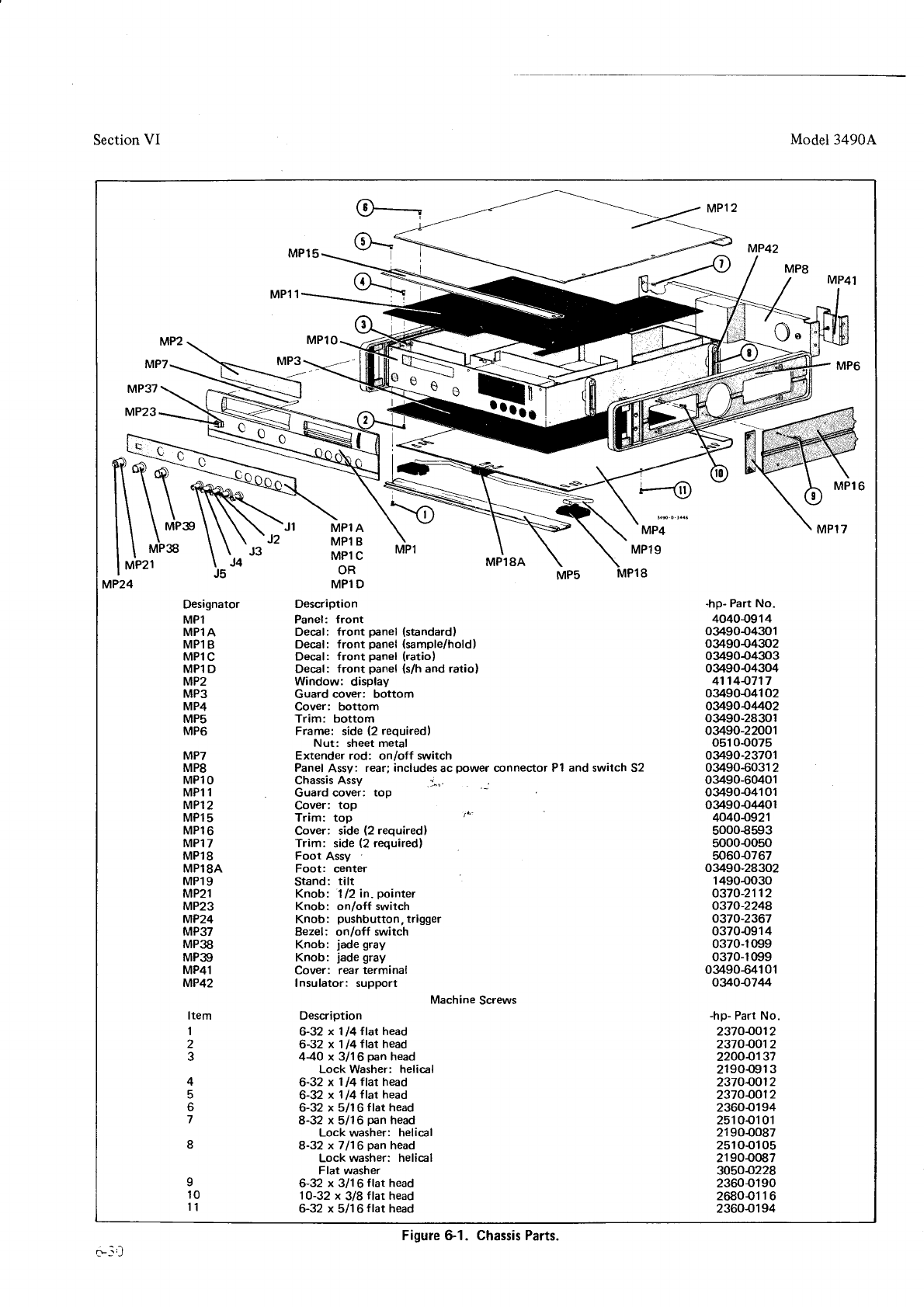
Section
VI Model3490A
h
MP7
MP37
MP23
Designator
MPl
MPlA
MP1
B
MPlC
MP1 D
MP2
MP3
MP4
MP5
MP6
MP7
MP8
MPl
O
MPl 1
MPl
2
MPl5
MPl
6
MPl7
MP18
MPl8A
MP19
MP21
MP23
MP24
MP37
MP38
MP39
MP41
MP42
Item
1
-hp-
Part No.
40400914
0349044301
o349044302
0349004303
0349044304
41
144717
o3/j9044102
03/9044402
o3490-28301
034,90-22001
051
0€075
03490-23701
034906031 2
03490-60401
03490041
01
0349044401
40404921
5000€593
5000{050
5060{767
03490-28302
1490{030
o370-2112
0370-2248
o370-2367
03700914
0370-1
099
0370-1 099
034909101
ouo4744
-hp-
Part No.
23704012
23704012
22004137
2190091
3
2370{012
2370{012
2360{194
251 0{1 01
21904087
25100105
21904087
30504228
2360{190
2680{1
16
23604194
2
3
4
o
7
8
Description
Panel: front
Decal: front panel {standardl
Decal: front panel (sample/holdl
Decal: front panel (ratio)
Decal: front panel {s/h
and ratiol
Window: display
Guard cover: bottom
Cover: bottom
Trim: bottom
Frame: side (2 requiredl
Nut: sheet
metal
Extender rod: on/off switch
Panel
Assy: rear; includes
ac power connector P1 and switch 52
Chassis
Assy t^..
Guard cover: top
Cover: top
Trim: top
Cover: side (2 required)
Trim: side (2 requiredl
Foot Assy
Foot: center
Stand: tilt
Knob: 1/2 in. pointer
Knob: on/off switch
Knob: pushbutton, trigger
Bezel: on/off switch
Knob: jade gray
Knob: jade gray
Cover: rear terminal
Insulator: support
Machine Screws
Description
6-32 x 1
14 flat head
6-32 x 114
flat head
440 x 3/16 pan head
Lock Washer: helical
6-32 x 114 flat head
6-.32
x 114 f
lat head
6-32 x 5/1
6 flat head
8-t2 x5116 pan
head
Lock washer: helical
8-32 x7116 pan
head
Lock washer: helical
Flat washer
63.2 x 3116
flar head
1
0-32 x 3/8 flat head
6-32 x 5/1 6 flat head
a
10
tl
N
Figure 6-1. Chassis Parts.
a--i,l
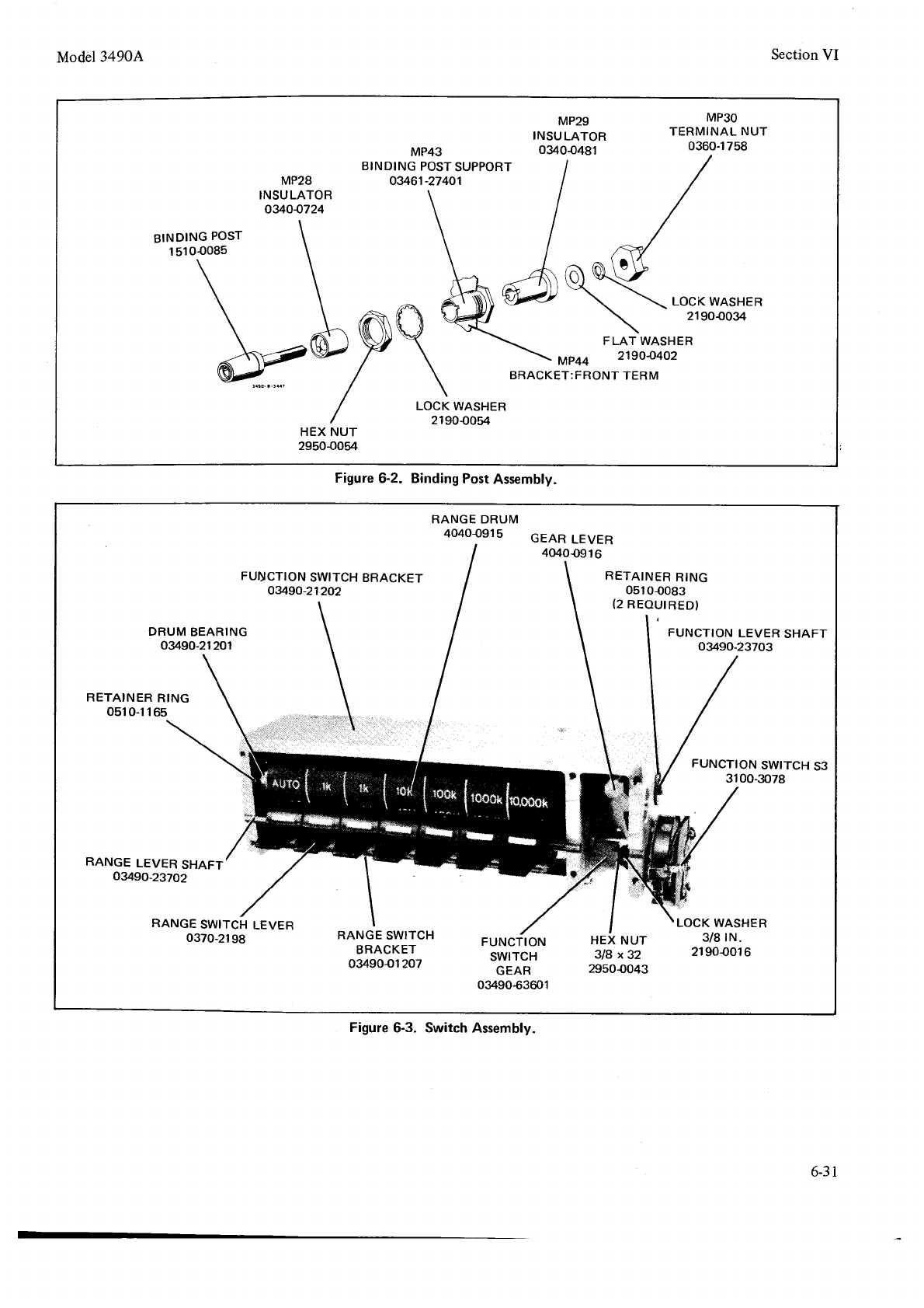
Model3490A Section
VI
MP2g MP30
INSULATOR TERMINAL
NUT
03400481 0360-1758
MP28
INSULATOR
03404724
BTNDING
POST
SUPPORT I /
03461-27401 ,
/
\l/
\t/
L ;oo-@
mft @v&'' \'o,%#'o'.x'^
P\ \*o0 '*i*o'"'*
\
BRACKET:FRONTTERM
BINDING
POST
1
51
00085
LOCK
WASHER
2190{054
HEX NUT
2950{054
Figure
6-2. Binding
Post
Assembly.
RANGE DRUM
4040{91 5GEAR
LEVER
40400916
FUNCTION
SWITCH
BRACKET
034,90-21202 RETAINER
RING
0510{083
{2
REOUIRED)
DRUM
BEARING
o3r'r90-21201 FUNCTION
LEVER
SHAFT
o3490-23703
RETAINER RING
o51 0-1 1
65
FUNCTION
SWITCH
53
3100-3078
RANGE
LEVER
SHAFT
03490,_23702
RANGE
SWITCH
LEVER
0370_21
98 RANGE
SWITCH
BRACKET
03490{1 207
FUNCTION
SWITCH
GEAR
03490€3601
HEX
NUT
318 x32
29500043
LOCK WASHER
3/8
lN.
21
90{01 6
Figure
63. Switch Assembly.
6-31
Model
3490A Section
VII
7.T.
INTBODUCTION.
7-2- This section contains information necessary
for
repairing
the Model 3490A. Schematic
diagrams, trouble-
shooting trees, and other troubleshooting and repair
information are
included. Figure
7-1 7 shows the location
of assemblies
within the 34904. Additional trouble-
shooting
notes are
located
on schematics.
7.3. PBELIMINARY
TROUBLESHOOTING.
74. lf the Model 3490A operates
incorrectly and the
trouble cannot be corrected by the Adjustment Proce-
dures,
the following troubleshooting
information
should
be used. Check
for loose wires or other obvious sources
of trouble, such as
burned
or loose components.
Make
sure
printed circuit boards are seated firmly in connec-
tors. Also make sure those microcircuit packages
that
mount in sockets
are
filmly seated.
7-5. TRO
UBLESHOOTING TREES.
7-6. Troubleshooting information for various circuits or
operations
of the 3490A is contained
in several
trouble-
shooting trees and associated
information. The General
Troubleshooting
Tree,
Figure
7-4,
may be
used to isolate
the problem
to a particular
area of the instrument.
The
following list indicates the circuits to which each tree
applies:
Troubleshooting
Tree
Title Figure
No.
Standard 3490A
Circuits
SECTION
VII
TBOUBTESHOOTING
AND
CIRCUIT
DIAGRAMS
7-7.
ACCESS
F0R
SERVtCtNG.
7-8. Access to most areas of the instrument may be
gained
by removing the top cover and the top guard
cover; It should not be necessary to remoye the bottom
covers
unless components
on the Main
Circuit Assembly,
Al , must be replaced. Remove
the top trim strip to gain
access
to the Display
Assembly. The three
vertical
screws
which secure the Display Assembly heat sink to the
guard shield
must be removed
in order to remove
the
Dsplay Assembly.
The
High Impedance,
AC Converter
and the
Ohms Converter printed circuit boards and
components must be kept clean and free
from fingerprints or other contamination, or
performance may be degraded.
Handle these
assemblies
by the board extractors.
7.9. POWER
SUPPLY CHECKS.
7-10. Check the power supply voltages
at the points
listed
in Table
7-1 using
an oscilloscope
and a dc digital
voltmeter with 4digit resolution. Voltage and ripple
specifications
are as shown. All ripple measurements
are
to be made
with the sample rate in the HOLD position.
Voltages are listed following the supply used as its
reference.
Therefore,
power supply voltages
should be
checked
in this order. The first supply checked wtrich
fails to meet the voltage specified is the faulty supply.
All supplies referenced to the faulty supply will also
,
indicate readings out of specification. With the faulty
supply
identified
proceed
to troubleshoot
as follows:
a. Pull opticns and install required
jumper
boards. If
problem disappears,
determine which option is at fault
and
proceed
to its troubleshooting
section.
Table 7-1. Power
Supply
Voltages and Gurrent
Limit Values.
General
DC Analog
AC Converter
Ohms
Converter
Display
Logic Test
hgic Clock
Option
021
Data
Output
Option 022
Remote
Option 030
cPrB r/o
Option
040
or 045
Sample/Hold
General
Sample/Hold
Logic
Option
080
Ratio
14
n<
7-6
7.7
7-8
7-9
7-ro
7
-lr
7-12
t-13
1-14
7-r5
1-16
Base
Supply
A1A,I
Test
Point Volrage Ripple
Current Limit
{Applox. Voltag€sl
+
17 V
+ 5V
+30V
-
17V
- 5V
-
30v
16.99 to + 17.0'l
V
4.995 to + 5.075
V
30.10 to+3O.9OV
'16.9 to- 17.1 V
5.00 to - 5.85 V
30.10 ro-30.90 V
< 50 mV p-p
( 60 mV p-p
< 25 mV p-p
<50mVpf
< 60 mV p-p
< 25 mV p-p
Al Rl04 = .434 V
A1R'l = .448 V
Al R11
'l
= 1.34 v
A1R118
= .54 V
41R125
=
1.30 V
Raw S0pply
Test Poinl Supply Voltage
Ripple
{Approx. Voltag€)
TPD
TPA
TPC
24V
24V
38V
38V
9V
24to+28V
24to- 28V
38to+44V
38to- 44V
9to+11V
I vp-p
t.2
v pf
.5VFp
.5 v p-p
1.5 V
p-p
1-l
Section VII
b. If the problem
is not with an option,
determine
if
the faulty supply
is
in current limit (see
Paragraph
7-12).
If so, determine where
the short is by use of the
power
supply
jumpers
and
troubleshoot
that section.
c. If the faulty supply is not in cunent limit,
determine if the faulty supply has
the correct
raw
supply
voltage (see
Table 7-l). ß the raw supply does not meet
specification,
troubleshoot this
section.
d. If the faulty supply is not in current limit and the
raw supply is within specification, troubleshoot the
faulty supply.
7-11. lf the + 17
V supply is out of specification
and
cannot be adjusted
per Paragraph
5-54, troubleshoot
according to Paragraph
7-10, steps a, b, c and d. It is
essential that the + 17 V supply
be within specification
since all other supplies
are referenced
to this supply and
will be affected. If oscillation
problems
are encountered
on the +l1Y supply,
change
AlClOg to 1000pF,
400
pF or remove from circuit. If there are ripple
problems on the + 17 Y supply or any other supply,
check to assure
the line voltage
selection
switches
are set
to correspond with available line voltage. If ripple still
exists, replace the filter capacitor of faulty supply.
Ripple problems
on the - 17 V supply
can
be caused
by
ripple or low voltage of the - 30 V supply Qower
voltage
than the
-24Y raw
voltage supply).
1-12. Nl power supply
regulators
are
current
limited so
that if an excessive
load is applied, the regulator
voltage
output goes
to neat zero. If this is suspected to be the
problem, the supply in current limiting can be deter-
mined by measuring
for the current
limit voltage
across
the resistor which are both specified
in Table 7-1.
Provision
has
been
made for isolating
certain
areas
of tfue
Main Circuit Assembly
by removing
designated
jump6r
wires in order to locate
the area
where
excessive
loading
occurs.
Table
7-2 lists
the jumper wire designations
and
the circuits supplied through each.
These
jumpers are
located on the Main Circuit Assembly,
Al and the
vertical board, AlAl. All of the Logic circuits are
supplied
through
only one
jumper
wire for each
voltage.
Consequently,
jumper wires are
provided
in the ground
circuits to isolated portions of the logic circuits.
These
ground
jumpers are shown on the schematic
diagrams,
Figure
7-23
andT-24.
7.13.
DC
ANAL0c
CtRCUtTS.
7-14. The DC Analog
Troubleshooting
Tree, Figure
7-5,
covers
the DC Amplifier, Integrator and Zeto Detect
circuits,
I l0 V References,
the DC Switching Logic
and
kvel Translators
and
the Power
Supplies.
7-15.
AZ
Asembly
Exchange.
7-16. Cleanliness
of the A2 High Impedance
Assembly
and the proper positioning of components on the
assembly
are
highly
important to the performance
of the
instrument. Also, A2U2 is very difficult to replace.
Consequently,
a rebuilt High Impedance
Assembly,
-hp-
Part No. 03490-69502,
has been made available to
Model
3490A
TableT-2. Power
Supply Jumper Wires.
Voltag€ Wire Location Circuits Supplied
+17V
+17V
+17V
-17V
-17
V
-17
V
-17V
+30V
+30V
+30V
-30v
-30v
-30v
+5
+5
+5
-5V
-5V
WH
w2
W6
wl
WEE
W3
ua
wz
WBB
W4
WAA
wcc
WFF
W7
WG
W5
WJ
W1
A1
A1A1
A1A1
A1
AI
A1A1
AlAT
AI
A1
A1A1
A1
A,'41
A1A1
A1
AlA.I
A1
A1
A1
Logic
t 10
V Reference
Integrator,
Zero Detect
logic
DC Switching
Level
Translators
tl0 V Reference
Integrator,
Zero Detect
Integrator,
Zero Detect
DC Amplifier
t 10 V Reference
Integrator, Zero Detect
DC Amplifier
DC Switching Level Translators.
A1CR403
Logic, Display,
Switches
Al U4Ol
,
O\rerload Protection,
DC
Switching Logic
Integrator, Zero Detect
Logic
Integrator, Zero Detect.
facilitate
repair of your 3490A when the trouble is on
the A2 Assembly.
Contact your nearest
-hp- Sales and
Service
Office for details.
7-17. DC Amplifier
Checks.
7-18. To check the DC Amplifier zero, set the Function
switch to TEST and select
Range
5. This grounds
the
amplifier input and sets
the amplifier
gain
to 100. The
front panel
display
should
be 000.000
1 15 counts.
To
check
for leakage current
in the input circuits,
compare
the numerical
reading in Test
5 to the reading in Test
6
with the input terminals shorted.
lf the reading in lest 6
is sömewhat higher
(igroring the decimal point), check
for leakage current.
Remember
that no soldering
should
be done on the A2 Assembly (see
Paragraph
7-14).
7-19. If the DC Amplifier cannot
be adjusted to zero in
Paragaph 5-60 step b, it is possible
that there
may be
leakage
to Guard from some point in the circuits.
Disconnect the Guard shorting
strap
from the input Low
terminal.
If the offset is
removed
or can
then
be adjusted
to zero, leakage to Guard is probable.
Some of the
possible
causes are: l) Breakdown
of the insulation
for
power transistor
Ql or CRl. 2) Leakage
to Guard
in the
power transformer. Disconnect
the small orange
wire
from the transformer cable to the solder lug on the
Guard
shield to check
this.
3) If the instrument
has one
of Options
020,021,022,030 or 040, there
may be
leakage to Guard on the isolation
assembly.
4) A wire
clipping
or other metal
chip
may
be wedged
between the
Guard shield
and the
Main
Circuit Assembly
Al.
7-20. Normal operating
voltages
wrthin the DC Ampli-
fier are shown
on the schematic
diagram, Figure 7-30.
To check the operation of various stages of the
amplifier, hrst set the Sample Rate control to HOLD
and disconnect
the Bootstrap
Amplif-ier
(white jumper
wire, labeled
"Bootstrap" on the Al Component Loca-
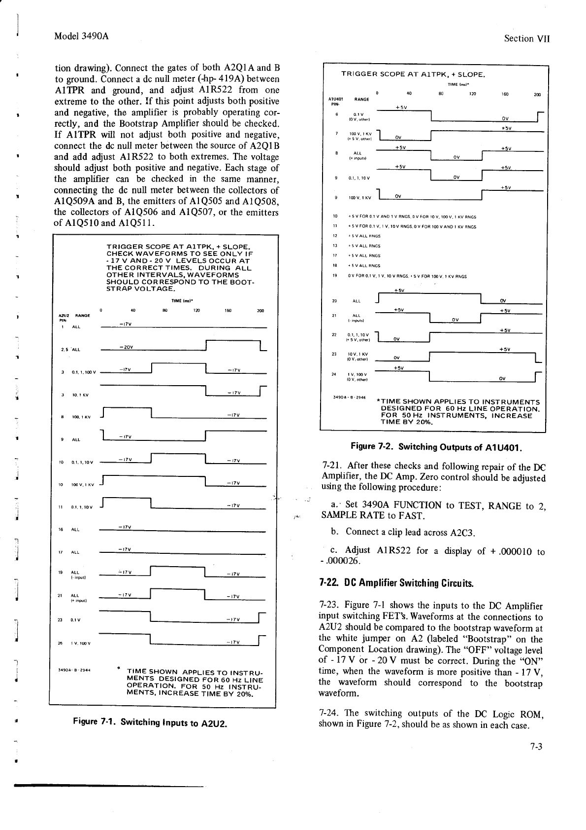
't
J
Model34904
tion drawing). Connect
the gates of both A2QIA and B
to ground.
Connect
a dc
null meter
(-hp-
419A)
between
AITPR and ground, and adjust AlR522 from one
extreme to the other. If this point adjusts
both positive
and negative, the amplifier is probably operating cor-
rectly, and the Bootstrap
Amplifier should
be checked.
If AITPR will not adjust both positive
and negative,
connect the dc null meter
between
the source
of A2Ql B
and add adjust AlR522 Io both extremes.
The
voltage
should adjust both positive and negative.
Each stage
of
the amplifier can be checked in the same manner,
connecting the dc null meter between
the collectors of
A1Q509A
and
B, the emitters
of A1Q505
and AlQ508,
the collectors of AlQ506 and AlQ507, or the emitters
of AlQ510
and AlQ511.
Section
VII
Figure
7-2. Switching
Outputs
of A1U401.
7-21. After these
checks
and following repair of the DC
Amplifier,
the DC
Amp. Zero
control
should
be
adiusted
using
the
following
procedure:
a.' Set 3490A FUNCTION to TEST, RANGE to 2,
SAMPLE
RATE to FAST.
b. Connect
a clip lead across
A2C3.
c. Adjust AlR522 for a display of +.000010 to
-.000026.
'l-22.
DC
Amplifier
Switching
Gircuits.
7-23. Figwe 7-l shows the inputs to the DC Amplifier
input switching
FET's.
Waveforms
at the connections to
A2U2 should
be compared
to the bootstrap
waveform at
the white jumper on A2 (labeled
"Bootstrap" on the
Component L.ocation
drawing).
The "OFF" voltage
level
of - l7 V or - 20 V must be correct.
During
the ..ON"
time, when the waveform
is more
positive
than - 17
V,
the waveform should correspond to the bootstrap
waveform.
7-24. The switching outputs of the DC Logic ROM,
shown
in Figure
7-2,
should
be as shown
in each
case.
TRIGGER SCOPE AT A].TPK, + SLOPE.
CHECK WAVEFORMS TO SEE ONLY IF
. 17 V AND. 20 V LEVELS OCCUR AT
THECORRECTTIMES. DURING ALL
OTHER INTERVALS, WAVEFORMS
SHOULD COR RESPOND TO THE BOOT.
STRAP VOLTAGE.
TIME
{ß1.
&1&til
&2 AAiGE
1 AtL -t7v
2.5 ALt
3 0.t,1,rmr
3 to,rKV
a t@,tKv
r0 0.1,
r,10v
16 ATL
19 ATL
2I ALL
23 0_l v
TIME SHOWN APPLIES TO INSTRU.
MENTS DESIGNED FoR 60 Hz LINE
OPERATION. FoR 50 Hz INsTRU-
MENTs, INCREASE TIME BY 2OOIO.
TRIGGER SCOPE AT A1TPK, + SLOPE.
Alu401
6
n
lii,,,
0.1, t. t0 v
10
tt
12
13
17
t8
l9
20
21
0.1, t. 10 v
'4eoa-a'2s46
*TIME sHowN AppLlEs ro TNSTRUMENTS
DESIGNED FOR 60 Hz LINE oPERATIoN.
FOR 50 Hz INSTRUMENTS, INCREASE
TIME BY 2Oolo.
Figure
7-1
. Switching
Inputs
to A2U2.
t-3
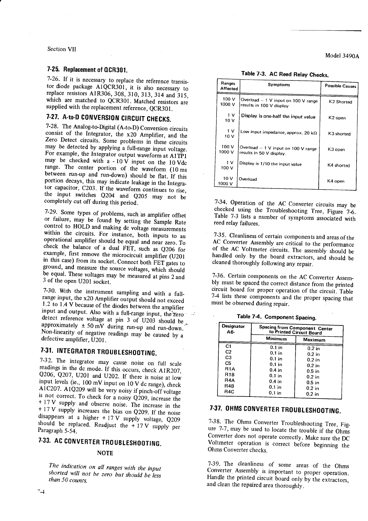
Section
VII
7-25.
Replacement
of OCR30l.
7-26. If it is necessary
to replace
the
reference
transis_
tor-diode
package
AleCR3Ol, it is also
necessary
to
replace
resistors
A1R306,309,
310,
313,
314
and
:t5,
which are
matched
to eCR3Ol.
Matched
resistors
are
supplied
with the
replacement
reference,
eCR30l.
7-21.
A-to-D
C0NVERSt0N
CtBCUtT
CHECKS.
7-28. Ttre
Analogto-Dgital (A_to_D)
Conversion
circuits
consist of the Integrator, the x20 Amplifier, and the
Zero Detect circuits. Some problern, in th"r, circuits
Tay be detected
by applying a full_range
input voltage.
For example,
the Integrator
output *"öfo.. at AlTpl
may be checked
with a _
lOV input on the l0Vdc
range. The center portion of the waveform (10 ms
between
_run-up and run_down) should be flat. if *ri,
portion decays,
this may_indicate
leakage
in the Integra_
tor capacitor,
C2O3.If the waveform
continues
to rise,
the input switches e20,1 and e205 may not be
completely cut off during this period.
7-29.
..Some
types
of problems,
such
äs
amplifier
offset
or failure, may be f9un9 UV setting the Sampte
Rate
control to HOLD and making dc voliage rn.urur"rn.nt,
within the circuits. For inslance, boih inputs to an
operational amplifier should be equal and near zero. To
check the balance of a dual FST, such u, qZOO fo.
example, first remove the microciriuit ampiifrer (U201
in this.case)
from its socket.
Connect
Uotf,'pfif gates
to
ground, and measure
the source
voltages,
which should
!" :gyd. These
voltages
may be *"urirrä at pins 2 and
3 of the
open
U20l socket.
7-30. Mth .the instrument sampling and with a full_
range
input, the
x20 Amplifier ouipuishould not exceed
| .2 to | .4
V because
of the diodes
i"t*..n tfr" amplifier
input and-output.
Also with a full_range
i"p"t, tfräZt,r"
detect reference voltage at pin 3 of*U203 should be
approximately 1 50
mV during run_up
una ,u"_Oo*n.,"
No^nJinearity
of negative
readiigs rnuy U, "uured by a
defective
amptifier,
ü201.
7.3I.
INTEGRATOR
TROUBLESHOOTING.
7-32. the integrator may cause noise on full scale
readings
in the dc mode.
If this occurs,
check
AlR207,
Q206, Q207, tJ2Ot and
u202.If theie i, noirc at low
input ievels
(ie., 100
mV input on l0 V dc range),
check
AIC2O7.
AlQ209 will be very
noisy
if pinch_äff
voltage
is not correct.
To check
for ä noisy eäOg, increuse
ttre
- !7y supply and observe
noise. The increase
in the
+ 17
V supply increases
the bias
on aZOS,li the noise
9Jt:qq.i" at a higher
+ 17
y ,upprv
-uoriuge,
e209
snoud be replaced.
Readjust the + 17
V supply per
Paragraph
5-54.
7.33.
AC
CONVEBTER
TROUBLESHOOTING.
NOTE
The indication on all ranges
with the input
shorted
will not be zero but should be'less
than 50 counts.
1:7
Model
3490A
Designator
A6- Spacin g_f
ro m corn ponäit-c"nt",
ro l,rtnted Circuit Board
Minimum Maximum
cl
c2
c3
c5
R1A
R1B
R44
R4B
R4C
0.1
in
O.1
in
0.1
in
0.1
in
0.4
in
0.1
in
0.4
in
0.1
in
0.1
in
O.2
in
u-2 tn
O.2
in
O.2
in
O.5
in
O.2
in
0.5
in
O.2
in
O.2
in
7-34. Operation of the AC Converter circuits may be
*::k.9,using the Troubleshooting
Tree, Figure 7_6.
Table 7-3 lists a number of symptöms
associated
with
reed
relay failures.
7-35. Cleanliness
of certain
components
and
areas
of the
AC Converter Assembly
are critical to the performance
of the AC Voltmeter circuits. The assembly
should
be
handled
only by the board extractors,
anä should be
cleaned
thoroughly following any repair.
7-36. Certain
components
on the AC Converter
Assem_
bly must
be spaced
the
correct
distance
from the printed
circuit board for proper operation of the circuit. Table
74 lists these
components
and the proper spacing
that
must
be
observed
during
repair.
. Table
74. Component
Spacing.
7-37.
OHMS
CONVERTEB
TROUBLESHOOTING.
7-38. The Ohms
Converter
Troubleshooting
Tree,
Fig_
ure 7-7, may be used
to locate
the trouble if tn. Onr
C-onverter
does not operate
correctly.
Make
sure
the DC
Voltmeter operation is correct before beginnrng
the
Ohms
Converter
checks_
7-39. The cleanliness
of some areas of the Ohms
C_onverter
Assembly
is important to proper operation.
Handle
the printed circuit board
only'by ihe extracton,
and
clean
the
repaired
area
thoroudily.
Table
7-3. AC Reed
Relay
Checks.
Ranges
Affected Symptoms Possible
Causes
100
v
1000
v
,IV
10v
IV
10v
100
v
ro00
v
1V
too
v
10v
r000
v
lOverload
- 1 V input
on 100 V range
I
results
in 1 00
V display
I
I DisOlay
is one-half the input value
I
I
I
Low input impedance,
approx. 2O kS-t
Overload
- I V input
on 100
V range
results
in
5O V disptay.
Display
is
l
/10
the
input
value
Overload
K2 Shorted
K2
open
K3 shorted
K3
open
K4 shorred
K4 open
:i
l
ii
j;
:l
.:'
a;
,'
.,1
,J
i
Model3490A
7.40.
DISPLAY
TRO
UBTESHOOTING.
741. "Ihe Display Troubleshooting
Tree, Figure 7-8,
mav be used io troubleshoot a defective display' The
nuäerical display units and the polarity unit may be
most easily
checked
by substituting
a known good
unit'
Access
to the Display Assembly is gained
by removing
the 3490A top trim strip and the tfuee vertical screws
securing
the diiplay heat sink to the guard shield'
742.
LOGIC
TBOUBLESHOOTING
SUGGESTIONS.
743. Several
microcircuits in the logic section may be
checked by observing the inputs and outputs of the
device. The "Q" output of a D flip-flop, for example,
should agree
with the "D" input if the flipflop is being
clocked.
(See
AlU6, 7, 71, 14, 17,20 md 22.) The
output is changed
by the "0" to "1" transition
of the
clock
input. Also,
the output of an inverter
(AlU8 and
10) should
be
the
logical
inverse
of its
input.
744. lf incorrect readings
are
observed on the logic test,
pull AlU2, 3, 9 and 16
and
reinstate,
taking care
to seat
leads
properly in their sockets.
AlU2,3, 9 and 16 may
be
checked by substituting
a known
good
device.
'745. Certain microcircuits may be associated with
particular
malfunctions.
A1Ul9 utd 2l deal with pro-
gramming
the 3490A range
and function.
AlUl5 and24
are associated
with sampling and sample rate delays.
AlUl5 also deals
with function delays.
746. If decimal point or ranging problems cannot be
located by using
the troubleshooting
trees,
the trouble
may be in the display, the front panel switching, or the
optional Remote Assembly. The decimal points in the
display are switched during the LOW true enable signals
to the display units (see
Figure
7-8).
747. If the instrument does not sample, the logic
circuits may be locked in a certain
state
or sequence.
Turn the instrument off. While holding the manual
pushbutton depressed,
turn the instrument back on anil.
observe the states
of logic signals
YMA through YMG
with an oscilloscope
(see
Figure 7-24). These are found
at test points O, T, P, S,
Q, N and
J
in the logic section
of ,the main circuit board. Test point O should
be a
steady
HIGH, and all others
LOW. If these levels
are.not
correct, the Read
Only Memory, AlU9, or one of the
State Storage flip-flops may be defective. If all seven
sigrals are correct, release
the pushbutton and check the
test points again with the oscilloscope.
If all levels
are
the same
as
before (TPO
HIGH and
all others
LOW), the
normally closed
contacts
of the pushbutton switch may
not be making contact. Check to see if the pushbutton is
binding in the center of the Sample
Rate
knob.
7.48. DATA
OUTPUT
TROUBTESHOOTING
(0ption
021).
749. Ceftan types
of failures
in the
output information
may be traced to certain circuits
in the Data Output
Assemblies.
Table 7-5 lists a number
of svmptoms and
Section VII
Table
7-5. Data
Output Troubleshooting
Tips.
Symptoms Probablo Cau$
Measurerent Intotmatioo:
No data output
No dab output and no polarity, overload,
or overrange
No odd numbers in any digit
No 2's,3's.6's, or 7's in
any digit
No 4's,5's,6'!, tr 7's in any digit
No 8's or 9's in any digit
Range Intorrotion:
No range data output
No range and no funcion data output
No odd numbered range data
Ranges 2,3, and 6 do not print correctly
Ranges 4,5, and 6 do not print correctly
Fundion lnformation:
No {unction data output
No tunction and no range output
Functions 1, 3, 5, 7,9, -, A, and * not correct
Functions 2, 3, 6. 7. +, -,
O, and * not correct
Functions4,5, 6,7, V. A, f|, and' not correct
Functions 8, 9, +, -, V, A, O, and i not corrrct
Polaritv, Overload, Overrange. Sample/Hold,
and Remote Mode Intormtion:
None of the above outputs correct
None oI the abow and no range output
No polarity output
No overload outPJlt
No overrange
output
No Sample/Hold Mode outPüt
No Remote Mode output
A9U9
A9U6
A10U1,2,3,7
A10U1
,2,4,7
A10U1,2,5,7
A10u1
,2, 6,7
AgU7
AgU6
41OU3
AlOU4
A1OU5
AgU7
A9U6
A1OU3
A1OU4
A1OU5
AlOU6
A9U7
AgU6
A1OUs
A1 OU6
A1OU3
AlOU6
A10U6
their probable
causes. Refer also to the Data Output
Troubleshooting
Tree, Figure
7-1
l.
7.50. REMOTE
CONTROL TROUBLESHOOTING
(0ption
022).
7-51. Refer
to the Remote Troubleshooting
Tree,
Fig-
ure
7-12, for information
for troubleshootine
the remote
control
circuits.
7-52.
cPlB
TROUBLESH00TtNc
(0ption
030).
7-53.
General Ghecks
7-54. lf the 34904 with Option 030 does not operate
correctly, first determine
whether the trouble is in the
I/O circuit or the main 3490A circuits.
The performance
checks in Section V may be used
to determine whether
the instrument
operates
properly in standard
multimeter
operation. Make sure the I/O plug-in printed circuit
boards are seated
properly
in their sockets, and that the
ribbon cable connectors are inserted properly. Also
make certain that all microcircuit packages
are seated
firmly in the sockets.
7-55. Troubleshooting Method.
7-56. The logic circuits which make up the GPIB option
are very difficult to troublestroot by the normal compo-
nent method
of troubleshooting.
Consequently,
a GPIB
Repair Kit, -hp- Part No. 03490-80009, has been made
available
to facilitate fast and efficient on-site
and bench
repair of the GPIB I/O Interface Option. The GPIB
Repair Kit consists of five assemblies
(*rp Part No.
0349G60613
, 46532, -66533, -66534
and
-66536),
and
six parts kits (hp Part No. 03490€0013, {0031,
-80032, -80033, -80034 and -80036), which are indi-
vidually available.
See Table 6-1 for description of
assemblies
and parts kits. This table also provides
a
7-5
Section
VII
breakdown of individual components contained in the
Repair Kit and their respective
parts kits. The printed
circuit assemblies
provided in the repair kit may be
substituted for assemblies
in the instrument in order to
isolate the trouble. A kit of microcircuit packages
for
each assembly
is provided so that once the trouble has
been
isolated to an assembly,
the defective microcircuits
on that assembly
may be replaced. A system controller
and a printer are required for troubleshooting the I/O
circuits. These
may be the controller and printer in the
system in which the 3490A is used. A dc voltmeter is
also required. The GPIB Troubleshooting Tree, Figure
7-13, checks
most of the
3490A I/O circuits.
7-57.
External
Trigger
Circuit Gheck.
7-58. The external trigger circuits may be checked by
the following procedure.
a. Place 3490L in local control by setting the
Remote
Control Enable line (LREN) to HIGH.
b. Set
front panel
SAMPLE
RATE control to HOLD.
Check logic level
of External Trigger
Flag
(LETF) at Jl I
pin 4. Measure
to outguard
ground
at pin 8 or 14
of Jl l,
or on Outguard Data Assembly A33. LETF should be
LOW until an external trigger
command is given.
If not,
check
A31Ql.
c. Momentarily connect Jl l pin 7 to outguard
ground. 349OA should sample each time pin 7 is
grounded.
If not, check A3lQ2 and associated compo-
nents,
including
pulse
transformer Tl. If the instrument
does
not have the Sample/Hold
option, a
jumper
should
be installed in place of Tl. Make sure this jumper is.
seated
properly in the correct sockets.
7.59. SAMPLE/HOLD
SERVICING.
7-60.
Acces
to
Sample/Hold Gircuits.
7-61. The Sample/Hold
Analog and Logic printed cir-
cuit assemblies, A27 and A28, are fastened together
and,
must be removed from their sockets as a unit. Printed
circuit extender boards (Part Nos. 5060-6032 and
5060-5983,
supplied
with the 3490A Option 040/045)
may be used to mount the Sample/Hold
assemblies high
enough for access to the circuits. The metal shield
covering
the Logic assembly may be removed without
separating
the two assemblies. Do not separate
these
assemblies
unless it becomes necessary in order to
replace
components.
The
Analog
Assembly,
A2T,especially
those
oreas
in the vicinit)' of the teflon insulators,
must be kept cleon and free from ftnger-
prints or other contamination, or Samplef
Hold performsnce
m6v be degraded.
Model3490A
742. lt it becomes
necessary
to separate the Sample/
Hold printed circuit assemblies
in order to replace
certain
components, it is preferable not to disassemble
more than necessary. For example,
if a repair is to be
made
to the Analog
Assembly,
A21,the flexible shield
should not be removed
from A28. If the unit has been
disassembled,
use the following procedure
and Figure
7-3 for reassembly.
a. Place Logic Assembly
A28 (item 3 in Figure 7-3)
component
side
down on work surface.
Place
4 spacers
(item 4) over the four captive spacers
in L28.
b. Carefully put flexible shield in place, aligning
holes in shield
with the
spacers.
c. Secure shield to A28, using two nylon screws
(item 6) in the two holes nearest the bottom edge of
A28.These screws
must be non-metallic.
d. Place two spacers
(item
4) on top of the
other
two
holes
in flexible shield.
e. Place
Analog Assembly,
A27, component side
up
over
the two spacers in step
d and
secure with the screws
(item 8).
f. Secure aluminum
shield
(item 2) over component
side
of A28, using four screws
(item l).
g. Connect brown,
red
and
orange wires
from A28 to
pins
l, 2 and 3,
respectively, on A27
.
7-63. 0perating
the 3490A
with Sample/Hold
Assem-
hlies
Removed.
7-64. lf a problem exists in the Sample/Hold
circuits
which affects
operation
of the 3490A with Sample/Hold
off, the S/H Analog and Logic Assemblies, A21 and
A28, may be removed and replaced by jumper boards,
which are
supplied
with the Sample/Hold
option. These
boards complete the circuits necessary to allow the
3490A to operate
(see
Figure 4-27). The wire discon-
nected
from the Analog assembly must be
connected to
the pin on the Analog Jumper Board for proper
operation.
Five pins
are also
provided
at the left end of
the Logic Jumper Board for terminating the wires
disconnected
from the Logic assembly.
These
pins are
not connected
to any
circuitry.
7.65. SAMPTE/HOLD
TROUBLESHOOTING
TREES.
l-66. Two troubleshooting
trees
are
provided
to assist in
isolating problems in instruments with Sample/Hold.
The S/H General
Troubleshooting Tree,
Figure
7-14,
is
designed
to determine
if the trouble is in the Sample/
Hold circuits
or in other circuits
in the 3490A. If it is
determined
that the trouble is indeed in the Samplei
Hold circuits,
this tree
will also
help determine
whether
it is in the analog
or logic circuits.
The Logic Trouble-
shooting
Tree,
Figure 7-15, provides further assistance in
isolating
trouble
in the Sample/Hold
logic circuits.
74
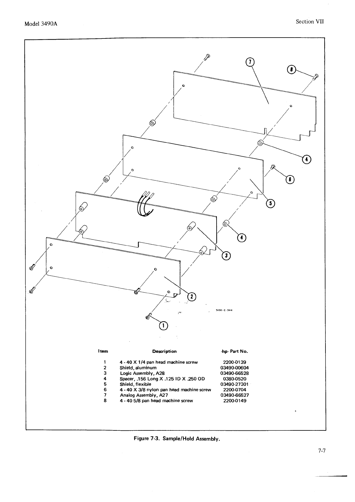
Model3490A Section VII
/
,.\
QY
//
L_/
\
Item
1
2
3
4
5
6
7
8
Description
4 -
40 X 114
wn head machine screw
Shield,
aluminum
Logic Assembly,428
Spacer, .156
Long X .125
lD X .250
OD
Shield,
flexible
4 -40 X 3/8 nylon
pan
head machine screw
Analog
Assembly,
427
4 -
40 5lA
pan
head machine
screw
trp- Part No.
220001
39
03490-006(M
03490€6528
03804520
o3490-27301
220047o'4
o3490€6527
2200.0149
Figure
7-3. Sample/Hold
Assembly.
7-1
Section
VII
7.67.
RATIO
TBOUBLESHOOTING.
l-68. If ratio measurements
are not correct and the
trouble cannot be corrected
by the Adjustment
proce_
dure, or if the adjustments
cannot be made
correctlv.
the following troubleshooting
information should be
used. Check for obvious sources
of trouble, such as
burned or loose
components
or loose
wires.
Make
sure
the printed circuit board, Al3, is seated
firmly in its
connector, and that the cable, W8, and the three
operational
amplifiers
are seated
firmly in their sockets.
7-69. External
Reference
Amplifier
Checks
7-70. The Ratio Troubleshooting
Tree, Figure 7_16,
checks the External Reference
Amplifier circuits. How_
ever,
correct
interpretation
of the display
symptoms
is
needed
to determine
if the trouble
is in the ämphner
or
logic circuits.
For example,
if the display
reads
approxi_
mately 75% of normal (l0V Input/tOV Exi. nef.
= 07.5000), the trouble is probably in the amplifier
circuits. If the display
reads
Overload
for both positive
and
negative
inputs (at INPUT terminals),
the
trouble
is
probably in the amplifier circuits, but if it reads
Overload
for only one
input polarity,
the trouble
is more
likely in the logic circuits. If the displayed
polarity is
incorrect and the display reads Overload,
check the
polarit
y logic
circuits.
7-71.
Amplifier
Zerc
0ffset.
7-12. lf the Reference
Amplifier zero adiustments
in
steps
a through h of the Ratio Adjustment
procedure
cannot be made
correctly,
the
trouble
may
be leakage
in
either AI3CR2 or 3. This
condition can
be most easily
checked by unsoldering
one lead of each diode and
trying the zero procedure
again.
If the
amplifiers
can
6e
zeroed with the diodes disconnected,
one or both of
them
is defective.
7-73. Reference
Polarity
Logic
Checks
7-74. ln the 3490A measurement
system,
if the Input
voltage is positive,
a negative
reference
is required
ior
run-down, and vice
versa.
In ratio measurements,
the
applied
External
Reference
voltage
is inverted
and these
two voltages
are substituted
for the positive
and negative
intemal reference
voltages.
The
Reference
polarity
Logic
on the Ratio Assembly,
A13, makes
it possible
to use
either polarity Externai Reference
inp,lt ,itt .itt u
polarity Input voltage
by selecting
the öorrect
reference
polarity for rundown. If a failure in the Reference
Polarity Logic causes
the reference
voltaqe used for
run{own to be the same
polarity as the Input, the
display will indicate Overloäd.
If the 3490A operares
correctly in dc voltage
measurements
with inputs of
both polarities.
but reads
Overload
with one polarity
input in ratio measurements,
check the Reference
Polaritl'
Logic
as
follows
:
a- Set
R{TIO switch
to EXT REF l0Vandapply
l0 \'to EXT REF
terminals.
--]
Model34904
b. Set FUNCTION to DC and
apply full-range
input
on either
the 1
V or l0 V range.
Select the
combination
of INPUT and
EXT REF polarity that causes
the display
to read
Overload.
c. Set SAMPLE
RATE to HOLD. Check
logic
levels
within Reference
Polarity Logic circuits as
indicated on
the schematic diagram, Figure j-22. Losic
HIGH
=
+
2.4V to
+
5 V. LOW
=
0 to
+
0.6
V.
7.75.
SCHEMATIC
NOTES.
7-76. tll.e following notes apply in general to all
schematic
diagrams:
a. Partial reference
designations
are shown. prefix
with asembly or subassembly
desigration(s)
or
both for complete
designation.
b. Component values
are shown as follows unless
otherwise
noted:
Capacitance
in microfarads
Resistance
in ohms
c. * Average
value
shown.
Optimum value
selected
at factory.
I
d. = Denotes
earth ground.
e. I Denotes
chassis
or frame
ground.
f. f Denotes
floatable
circuit
ground.
.9. qP Denotes
printed
circuit
assembly ground.
-V
k.
Denotes
assembly
outline.
Denotes
subassembly
out-
line.
Denotes
main sigral path.
Denotes
feedback
path.
l. l------l Denotes
front panel
markings.
Denotes
screwdriver
adjust.
n.Wl Denotes
wire color. Color code
is the same
as the resistor color code. First number
identifies the base
color; second
identifies
the wider strip; and third number
identifies
the narrower
strip (e.g. 924 = white,
red,
yellow).
" 3 Denotes
schematic
number
on which
con-
Y nection is maije.
p. A Refer
to
manual
backdating,
Section
VIII.
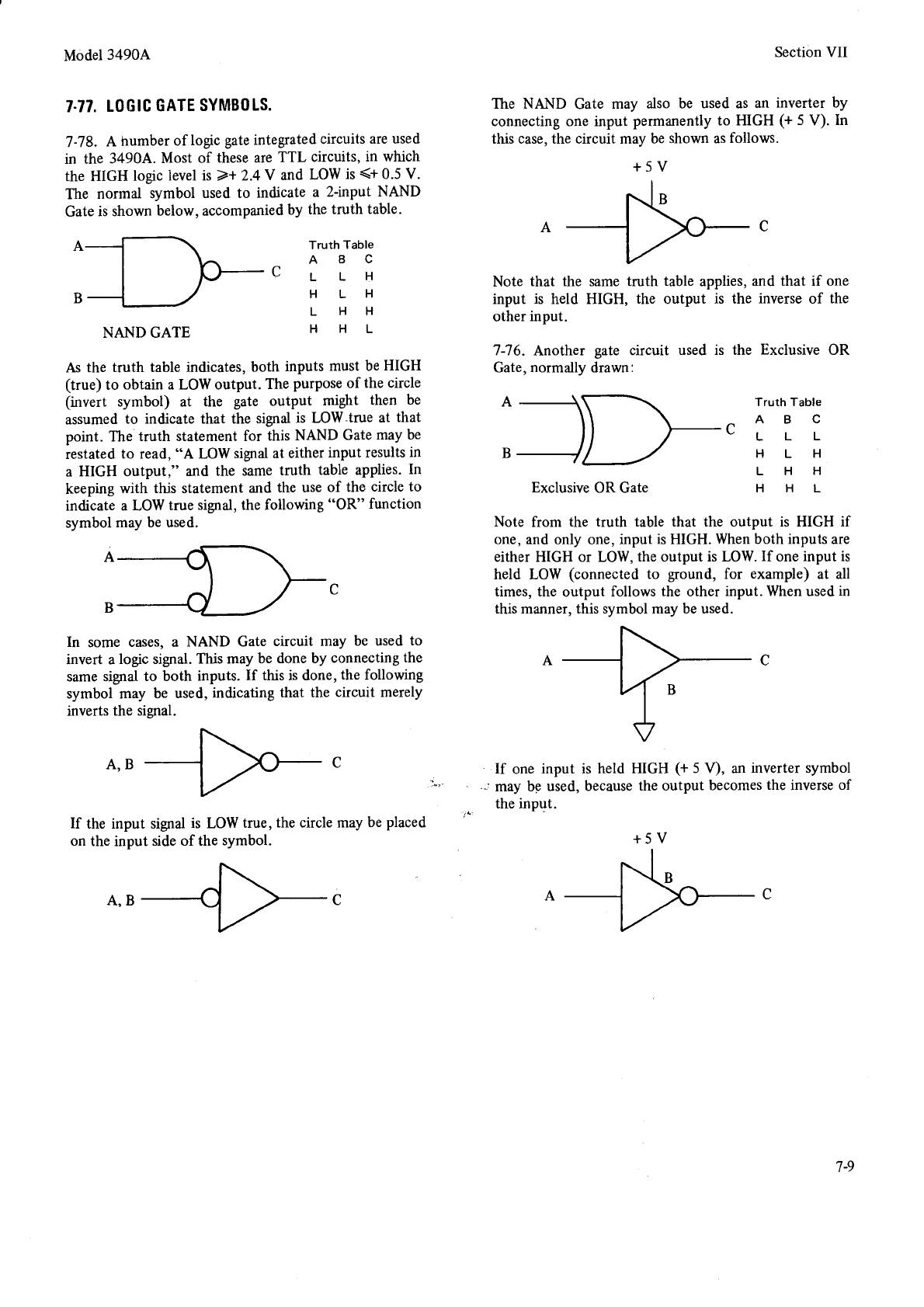
Model3490A
7.77.
LOGIC
GATE
SYMBOLS.
7
-78. L humber
of logic
gate integrated
circuits
are used
in the 3490A. Most of these are
TTL circuits,
in which
the HIGH logic level is 2+ 2.4
V and LOW
is (r 0'5 V.
The normal symbol used to indicate a 2-input NAND
Gate
is shown
below, accompanied
by the truth table.
NAND GATE
Truth
Table
ABC
CLLH
HLH
LHH
HHL
As the truth table indicates, both inputs must be HIGH
(true)
to obtain a LOW output. The
purpose ofthe circle
(invert symbol) at the gate output might then be
assumed
to indicate that the signal
is LOW true at that
point. The truth statement for this NAND Gate
may be
restated
to read,
"A LOW
signal at either
input results
in
a HIGH output," and the same
truth table applies.
In
keeping with this statement and the use
of the circle to
indicate a LOW true sigtal, the following "OR" function
symbol
may be used.
In some cases, a NAND Gate
circuit may be used
to
invert a logic signal.
This may be done by connecting
the
same sigral to both inputs. If this is done,
the following
symbol may be used,
indicating that the circuit merely
inverts the sienal.
If the input sigral is LOW true, the circle may be placed
on the input side of the symbol.
Section VII
The NAND Gate may also be used as an inverter by
connecting one input permanently to HIGH (+ 5 V). In
this case, the circuit may be shown as
follows.
Note that the same truth table
applies,
and that if one
input is held HIGH, the output is the inverse of the
other
input.
7-76. Another gate circuit used is the Exclusive OR
Gate,
normally
drawn:
A
A
Exclusive
OR Gate
Truth Table
ABC
LLL
HLH
LHH
HHL
Note from the truth table that the output is HIGH if
one,
and only one,
input is
HIGH. When both inputs
are
either HIGH or LOW,
the
output is LOW.
If one input is
held LOW (connected
to ground, for example) at all
times, the output follows the other input. When used in
this manner, this symbol may be used.
If one input is held HIGH (+ 5 V), an
inverter symbol
-,
may bg used, because
the output becomes
the
inverse
of
the input.
+5V
+5V
7-9
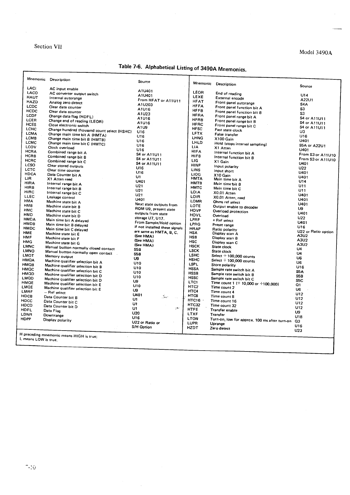
Section
VII Model
3490A
Table
7-6. Alphabetical
Listing
of 34g0A
Mnemonics.
Mnemonic Description
LACI AC input enabte
LACO AC conwrter output switch
HAUT Internal
autorange
HAZD Analog zero
detect
LCDC Clear
data counter
HCOC Clear data counter
LCDF Change
data ftag (HDFL)
lgER Change
end of reading
{LEORI
HCES Close
electronic
switch
f9!C Change hundred thousnd count select
f9yA Change
main time bit A (HMTA)
i9yg chanse main time bit B (HMTB)
l9yc Chanse
main time bir C (HMTC)
LCOV Ctock overtoad
HCRA Combined range
brt A
HCRB Combined range
bit B
HCRC Combined range
brr C
LCSO Clear
stord outpurs
LCTC Clear
time @unter
HDCA Data Counter bit A
LIR Xt Atten reed
HIRA Internal range
bit A
HIBB Internal
rarEe
bit g
HIRC Internal
range
bit C
LLEC Leakage
control
HMA Machine
state
bir A
HMB Machine
state
bit B
HMC Machine
state
bit C
HMD Machine
state
bit D
ly9A Main time bit A detayed
Iy?q Main time bit B detayed
Iy?C Main time bit C detayed
HME Machine
state
bit E
HMF Machine
state
bit F
HMG Machine
state
bit G
ryryg Manual
button normaly ctosed
contact
ly!9 Manuat
button normaily open contact
LMOT Memory output
llygf Machine
quatifier
setection
bir A
ly99 Machine
quatifier
setectaon
bit B
ly99 Machine
quatifier set&tion bir C
lIgD Machine
quatifier setection
bit D
.:yy? Machine
quatifier
setection
bit D
:y:_a Machine
quatifier setection
bit E
:yy: Machine
quatif
ier setection
bit E
LMRF - Ref select
HOCB Data Counter bit B
HDCC Data
Counter
bit C
HDCD Data Counter bit D
HOFL Data
Fte
LDNR DownraÄe
HDPP Oisplay p-olaritv
Source Mnemonic Description
Aru4ot lr_eOn
Al u401 | r_exe
From
HFAT
or
Al 1 U1
I I grar
41U203 | rrra
41U16 | Hrra
A1U23 | xrne
Alu16 | nrne
A1U16 | srnc
Alus l nrsc
(HSHC) U16 t LFTX
u16 l r-nrvc
u16 llrr_o
u16 llre
u16 lHrre
54 or
AtlU1
I I Hrre
S4orA11U11 lltC
54orAllul1 ltrnrp
Y19 | r-r'vs
Yl6 | r-roc
ul I ilr.are
u401 | xMre
u21 | xrvrrC
u2t I lore
u21 | lorn
u4o1 | r-orurn
Next
stare
outputs
from I iors
BOM
U9,
present
state I frovp
outpurs
from
state I Hovt_
storage
U7,
U
17. I f_pnf
From
Sample/Hotd
option I f_pnC
if not instailed
these
signats
I ffnep
aresmeasHMTA,B,C. I HSn
(se HMAI I HSe
(See
HMA) | rSC
(See
HMA) | HSCK
s58 | LScx
ssB I 1-5nc
r,!r I usnc
ulo I r_spr_
ulo I usse
u10 | HSSB
u10 | HSSC
ue I lrcr
uto I Hrcz
u9 | srca
u401
ul I Hrcl6 .
ul I Hrca2
ul " I Hrrs
uzo I LTXF
u16 I lroru
U22
or
Rario
or I r-Upn
s/H
oprion I nzof
End of reading
External encode
Front panel
autorange
Front panel
function bit A
Front panel
function bit B
Front panel
range
bit A
Front panel
range
bit g
Front panel
range
bit C
Fast
state
clock
False
transfer
Xl0O Gain
Hold (stops
interwl sampting)
Xl Atten
Internal
function bit A
Internat
function bit B
X1
Gain
Input polarity
Input short
X10
Gain
Main
time bit A
Main time.bit B
Main
time bit C
X0.01 Atten
X0.01 Atten, reed
Ohms ref select
Output enable
to decoder
Overload protection
O\rerload
+ Ref select
Preset
range
Ratio polarity
Display
scan
A
Display
scan
B
Oisplay
scan
C
State clock
State
clock
Select
+ 100,000 counts
Select
+ 1OO,0OO
@unts
Store polarity
Sample
rate
switch bit A
Sample
rate
sitcfi bit B
Sample rate ilitch bit C
Time count 1 (+ l0,OO0
or +l@,OOOI
Time count 2
Time count 4
Time count I
Time
count l6
Time count 32
Transfer
enable
Transfer
Turnon, low for approx. 100 ms
after turn-on
Uprange
Zero detect
Source
u14
422U1
s4A
S3
s3
54 or
A11U11
54orAltUl1
54or41tU11
U3
u16
u401
S5A
or
A22U
l
u401
From
53 or
At
t UlO
From
53 or
At l
UtO
u401
U2?
u401
u40l
ul4
ul1
ul 1
u401
u401
u401
U9
u401
u22
u401
ul6
U22
or
Ratio
option
A3U2
A3U2
43U2
v4
U4
U6
U6
ul6
s5A
s5B
s5c
Q1
U6
u12
u12
vl2
U9
u18
o3
ul6
u23
H preceding
mnemonic means
HIGH is
true;
L means
LOW is
true.
- 1i,
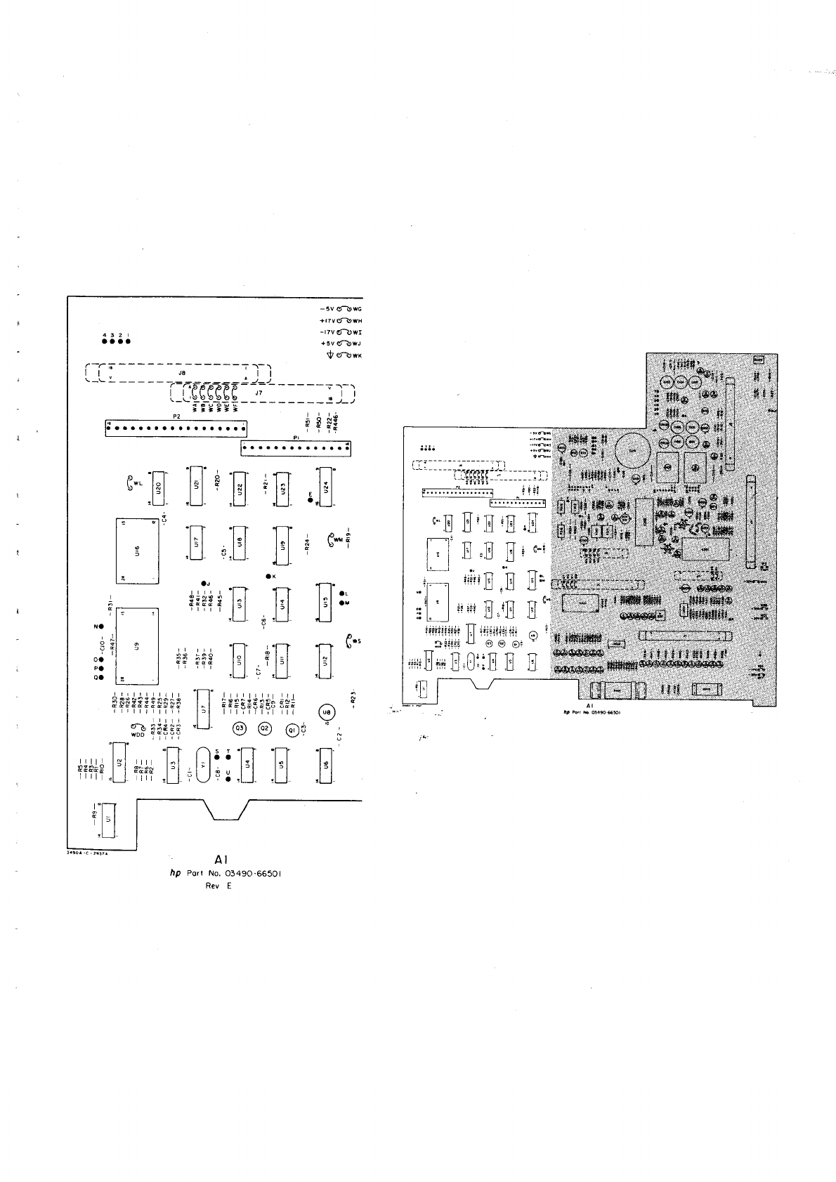
- 5v c-u wG
+r?v6-UwH
43zt -t7v6\wr
aaaa +5vcttwJ
f <r-uw*
a--;--- --ir-\
ll J8 ^ll
-
- - : - - - - - =: iaF{eV-pF
-t =,:'- - - - - - r t- )
i_.,gu_spb b _ l'_ _ _ _ _ _ _ " )_ )
]'-].i
Dtl
S*' lR I
lrl
!U_ E*E
JPI
1..
...... o. ....1
'n"
ll
E
t-l
."1 |
'ft^ 'n^
lFl lol
l5l l5l
,Ll q,LJ_
AI
,rp Port No. 03490.66501
Rev E
Tt"
töl
l=l
il-
']-J
l-l
i
aJ
r,,, r
'[J
.-;*s I l. l
",'rl-l
T_l'
I laL
lil o,
t-l
li.l
D
.TT \)
tNl
l-l
!u-
tv
'ft'
tl
I'l
tl
!U
rn
T
l-l
,L_J
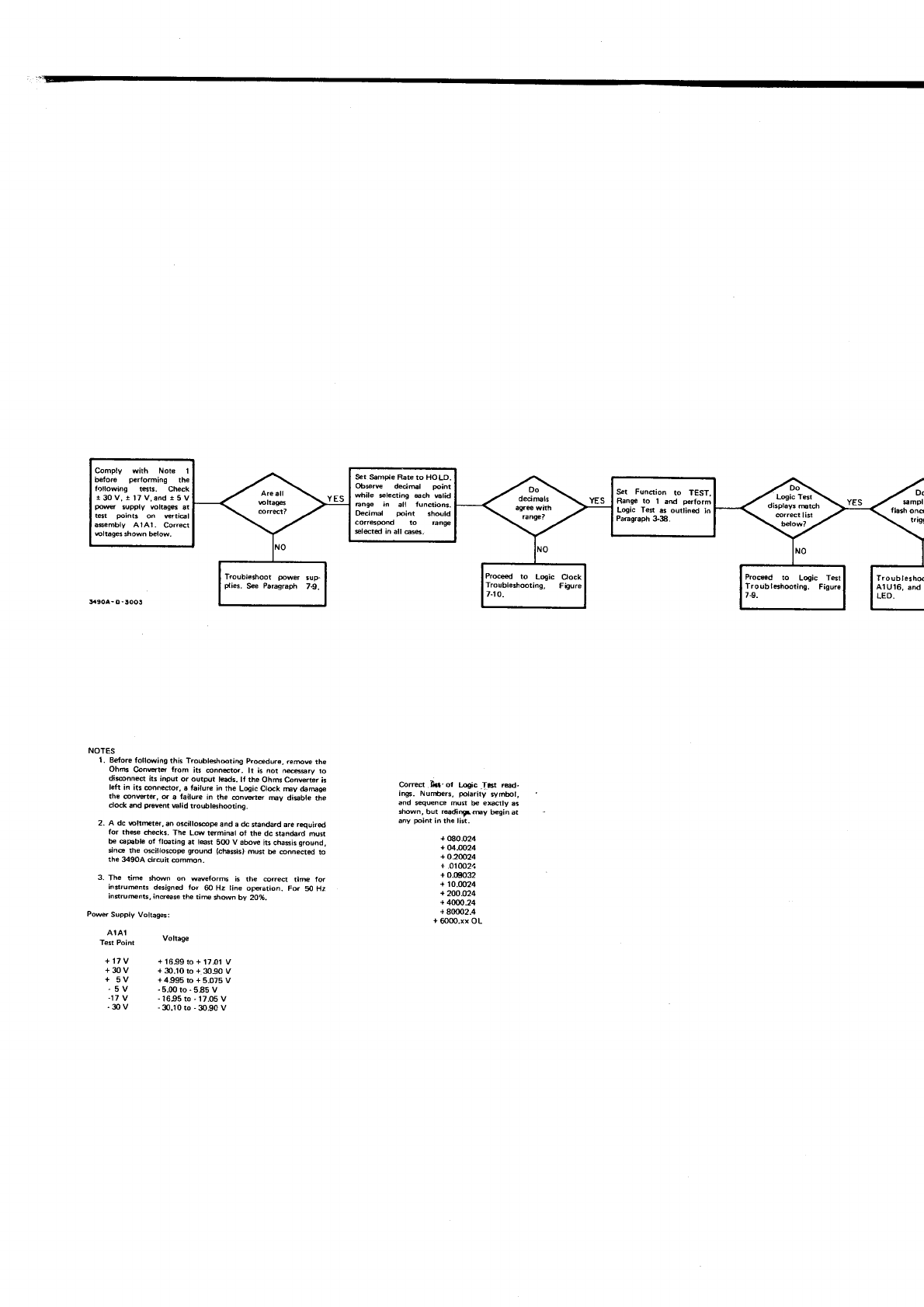
Comply with Nots 1
betoro frforming the
following t6ts. Check
r 30 V, I 17 V,and r 5 V
prer suppty vott6g6 at
6t pints on sti€l
a$embly 4141. Correct
Eltages shown below.
Set Sbmple Rate to HOLD.
Obsrw decimal pint
while *lecring ech 6lid
EnF in all fundions.
Oecimd Fint 3h@ld
corrqpd to rans
elfttd in all 6s6.
Set Fundion to TEST,
Range to 1 ad Frform
Lqic Ten $ ou{ind in
Pa€graph 338.
!904- O-!OO!
NOTES
1. Bdore lollowing this Troubleshmtiru Proedure, .emve th€
Ohc Oonvqtq from it3 @nndor. lr is nor n*6erv ro
disnned iis input or outpur tads. tf the Ohft Convener is
lefr in its 6nnedor, e tailure in the Logic Ct@k my daroS
the @n6er, d a Iaiture in the 6nsts my diebt€ the
clock and Fovent Elid tro6tsh@trn9.
2. A dc Fltretn, an osdtto@f and a dc srandard are rquired
for th6e ctekr. The Low ltrminat ot the dc standard most
h 6Fble of fl@ting at l@st 50O V abow its chasis ground,
sine th€ oscillosof ground (clEssisl mult b dnnedd to
the 34904 cLcuh @mmon.
3. The time shM on wavelorms is rhe corred tiru fot
infrumnts designed tor m Hz tine o6ation. Fff 50 Ht
in*rurunts, increase rhe time shmn bv 2O%.
Powtr Supply Voltages:
AIAI vona@
+17V +16!9to+17.01 V
+ 30 V + 30.10 to + 3090 V
+ 5V +4995to+5.075V
- 5V -5.O0to-585V
-17 V - 1695 to - 17.05 V
- 30 V - 30.10 to ,30.90 V
Cored Dd ot Logic .T.
6t r@d-
ings. Numbers, rclarity rymbol,
and sequen@ mu$ be ebctly as
shown, but r€adinfr my b€gin at
any Fint in the lirt-
+ @0.024
+ o4.oo24
+ o.2@24
+ .01002/i
+ 0.09032
+.t0.0024
+ 200.024
+ 4000.24
+ 80002.4
+ 6O0O.xx OL
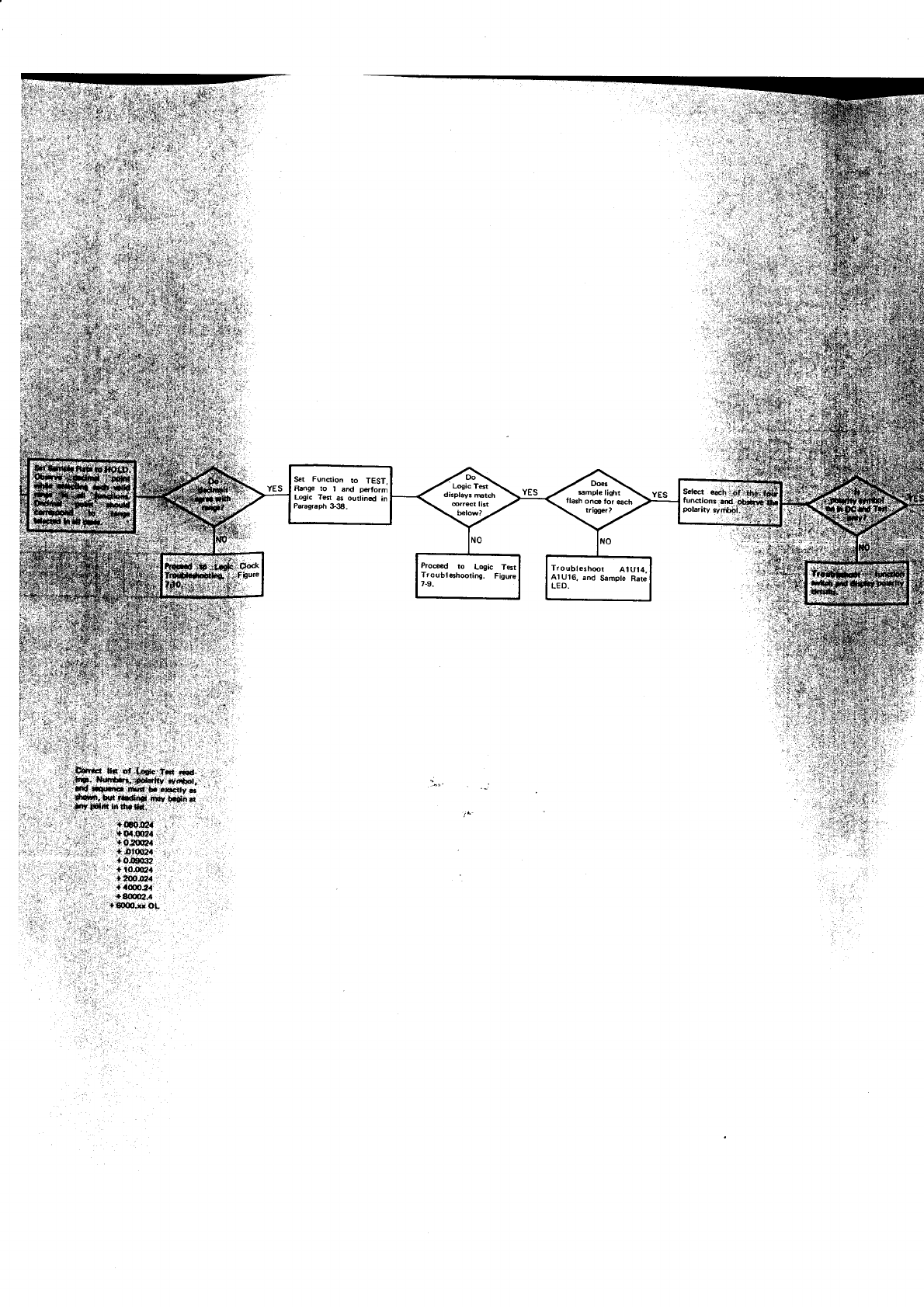
-,
.'i .:
':
::
;.:
,]
,i
.:*,
':,il: ':'
.:
'i
i1
:L;gji,
,
.!-.-,'
til
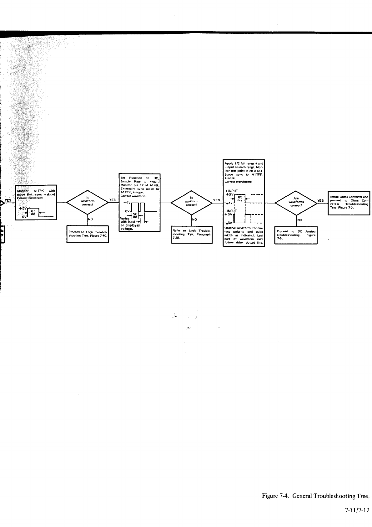
Apply I /2 full range
+ and
- input on e*h Enge.
Mon-
itor t$t rcint g on A1A1.
S@pe rync to A'TPK,
+ slope.
Correct
wadorft:
I
tl
-INPUT I
+3vri I
IL_J]:
Obs€re waveforG for @r.
polaraty 3d rul*
6 indi6td. lr.t
F t of ffivelorm my
follow oirher dortd line.
+ INPUT
St Fundion to
Smde Rat€ to FAST
pin 12
ot AltX)
AITPK. +
stooe.
JIIIL-
,"."i1glil
rilh i.9uli F
or disploy€d
ü*!iai ott"" *nn
!drp6 ltnt. rync,
+.1@)
@ect trvefo.d:
Proceed to Logic Trouble-
$@ting Tre, Figure 7-10.
Refer to Logic Trouble-
*Foting Tips, ParagEph
7-3}.
Figure 74. General
Troubleshooting
Tree.
7-rt
l7-r2
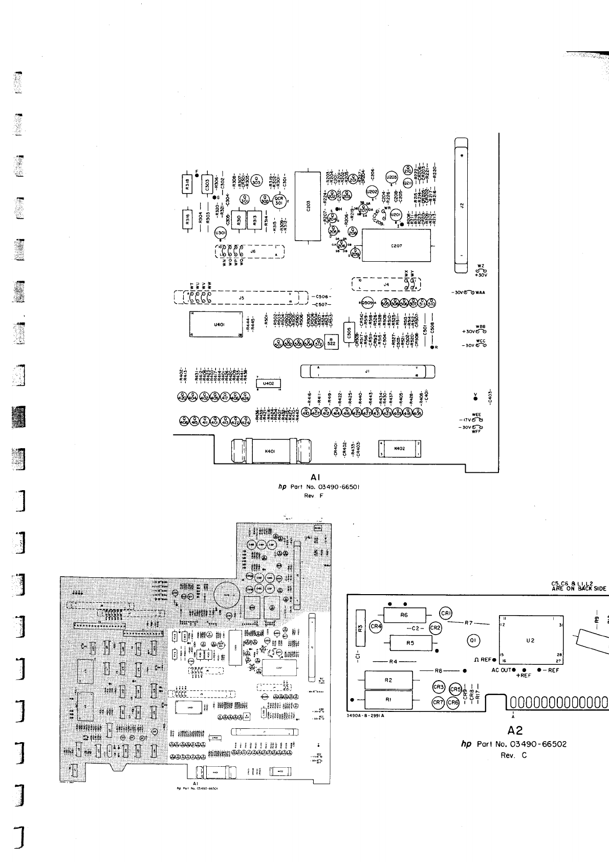
-:=i:E
::.: !.
+esr;$o!cl
e
8+*++
*
*@$@
Fr*$$-++Wi*
el *is'*;$9.
++++gp++
g.@
ll?Qxl c2or i-
c207
i*l'ril+*
$?B?@ ä?FF
UI\
, ]'i*B
@ @'@'
A | | *$ .-t-.J-, -,
l;l
a r
-'tl
a
ll
i
l* ; or
?1t61
l7+Ti+?
\J
.67j7,'66:-----\
l.
$!9b-
i"- - -:.,1
zOao
l;i;
.
i
:F
.i.s
ä
T
.-+i:
.'..s
s$sE
IJ-* I
AI
äp Port No.
O349O-66501
Rev F
-.n
,l
J
ffi
:'
l
3
,3
3
l
3
3
l
0000000000000
c5,c6 I Lt.L2
ARE ON BÄCX SIDE
:3t:
tr'.n
hp Pott No.
0349O-665O2
Rev. C
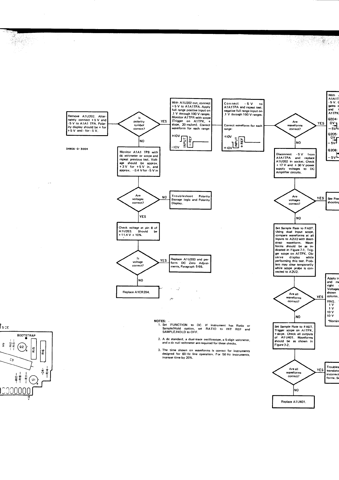
l: r.f:
YES
with /
AIAlTI
-5V.
C
gac3 o
arld (
AlTPK]
Q204:
oVr
r
-uiL.r
Q205:
orr:
-sVJ I
See Ptu
*poring
Q208:
F
_5VL
'++
@"Un
\o?
NOTES:
1. Ser FUNCTION ro DC. lI inslrument has Ratio or
Sample/Hold option, set RATIO to tNT REF and
SAMPLE/HOLO ro OFF.
2. A dc *andard. a dual-race o$illosp€, a 5diqit sltreter,
and a dc null rcltmeter are required for thee checks.
3. The time sh&n on wawforms is @Fect for instrurenti
dsigned for 60 Hz line opeEtion. For 50 H. instrumnts_
ins€s time trv 20%.
YES
T.oubleC
YES I ranCaror
In@rrcct
forc. S€
Apply in
and ft
right (
Voltag6
@rumn.
RNG. I
'tv
10v
tov
'Nofünr
With Al U202
out, connect
+ 5 V to A'l41TPA. Appty
tull range p6;tive input on
.1 V through l0O V r.ngs.
Monitor A ! TPR with scop€
lTrigge. on AtTpK, +
slope, 20 ms/cm). Cdrect
wavetorm for @ch range:
Connect -5V to
AIA1TPA and repqr t6t.
negatiw full Enge input on
.1 V through 1O0 V range..
Correct waveform Ior each
6nge:
Remve A1U202. Alte-
nately @nnect +5 v 6nd
-
S V ro AlAl TPA. Potar-
ity display shoutd be + for
+5V and-for-5V.
Moniror AlAl TPB with
dc wltmeter or scope and
repeat .pfevaous
test, volt-
age should be apfox.
+3V for +5V in, and
approx. -0.4Vtor-5Vin
Disnned -5V lrom
A1A1TPA and repl@
A1UZ)2 in scket. Check
jlTV.nd !30Vpow6
supply wlbg6 ro DC
Amplifier circuits.
Check @ltage at fin 8 of
AlU2O3. Should be
+11.4Vi10%.
Set Sampte R.E ro FAST.
usang dual inpu! spe,
@mp6re waveform 6t all
input. to A2U2 with B@t-
$6p waveform. Waw-
torß Crould be aa in-
in Figure 7.1, Trig-
s@r on AITPK. Ob-
serve display while
performing rhia tes. Prob-
lem mV clear temporarily
while r@pe probe is @n-
n4ted to A2U2.
Replace A1U2O3 and per-
torm DC Zero Adiu.t-
rcnts, Pa.agraph 5€5.
Set Sample Rare ro FAST.
Trigger $ope on AITPK.
+ilope. Check all outpuls
ot Al U401. Wavelorms
*lould be ar shown in
Figure7.2 -
54904 -O- 3004
,
r
s tE
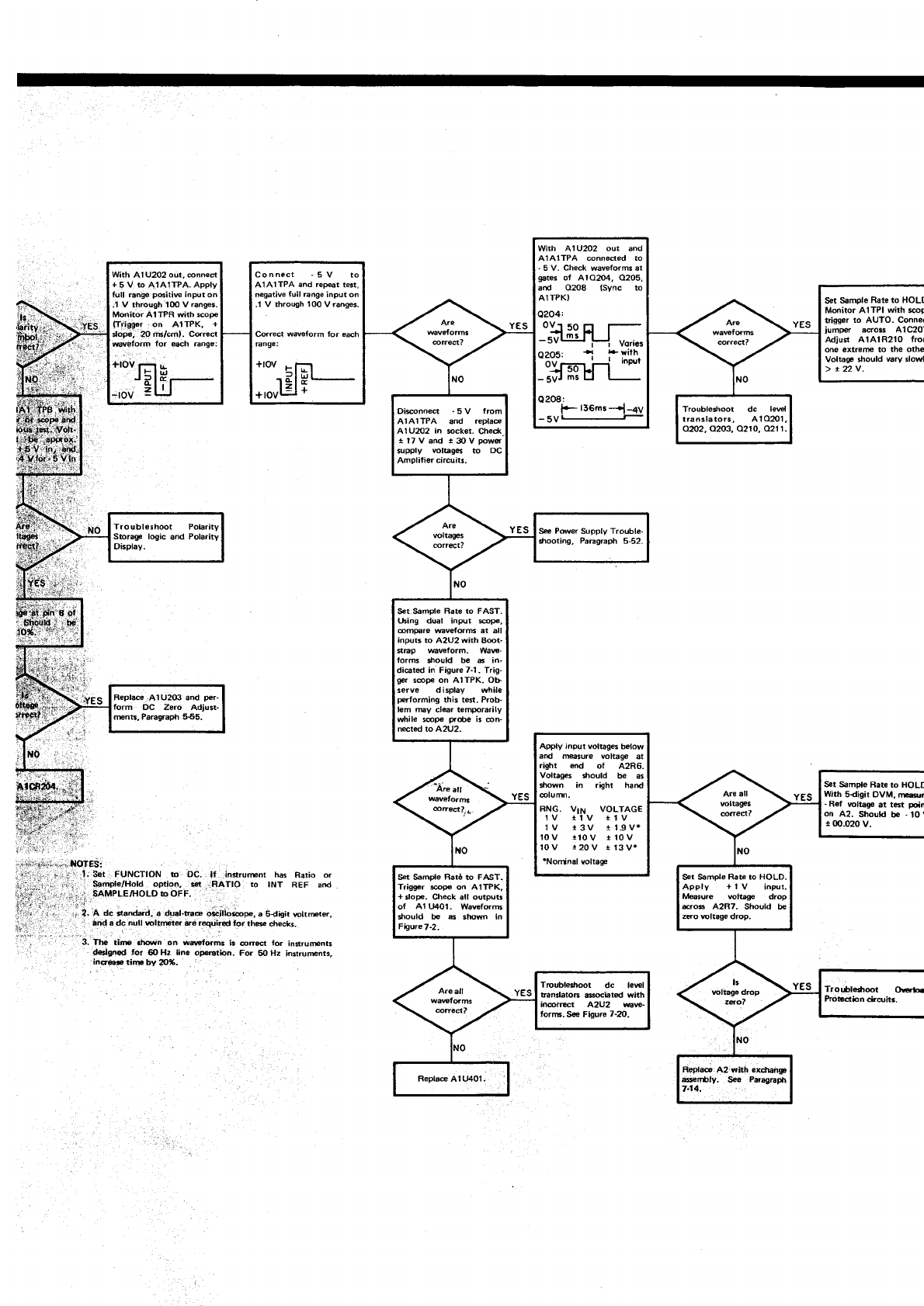
With AlU2O2 out and
AIAlTPA conneded to
- 5 V. Check waveforms at
gates oJ AlO204. 0205,
aod 0208 lSync to
AlTPK)
Q204:
"HÄqfr"
Q2O5: t1 swith-
:irsul-
Ft36msi_4v
-5V' -
With A1U2O2 out, @nnect
+5V bAIA|TPA.Apply
full range pGitiw input on
.1 V through 100 V ranges-
Monitor AITPR with scoF
fr{999l on AITPK. +
{ope, 20 G/cml. Csßd
Mvetorm for qch Bnge:
Connect -5V to
AIA1TPA snd rep@t t6t,
negative
full range
input on
.1 V through 100 V ranges.
Cdrect wavoform foa each
Engei
Disnnect -5V from
AlA'ITPA and reDla@
A1U2O2 in scket. Ch€ck
t '17 V and r 30 V pow6
npply rclbgG to DC
Amglifi6r circuiti.
Troubleihoot dc level
trä6slator., A1O2Ol,
a202, amq 0210, @11.
Troublesh@t Pohrity
Sbrage logic and Polaritv
Diiplay.
See
Pder Supply Trouble-
Öooting, PaEgraph 5-52.
Set Sample Rate to FAST.
t sing dual input sp€,
6mp6.e mveform at all
inouti to A2U2 wirh B@t-
s6p Mwform. YVaw-
fords *rolld be 6 in-
di€ted in Figure 7-l - Trig'
g€r s@pe on AITPK. Ob-
ierve display while
performing this td. Prob-
lem my cl€r tempora.ily
while s@po prde ir @n-
neted to 42U2.
Repla@ .Al U2(Il and p€r.
form DC Zero Adiurt
rcn$. Pa6graph 5€5.
Apply input volbges below
and t@sure voltage at
right sd of A2R6.
Voltag€s should be as
*Ewn io right hand
@|uffi.
BNG. V11 VOLTAGE
lv ilv rlv
tv t3v rt"9vr
10V iloV t 10V
10v r20v r13v*
'Nodi^al roltage
Set S6mple Ratö to FAST-
Trigg€r spe on AITPK,
+.lope. Check .ll output
of Alt401. Wawform
$ould be ei sh@n in
F'rlure 7-2.
Set Sample RaE to HOLD.
Apply +1V inrt,
M@süre rcltage drop
dos 42R7. Should b€
do rcltaqe drop,
Trcubl€Cr@t dc lewl
tarclatoc asiated with
inddd A2U2 GG
to.c, Se Figure 7-?O.
R€pla@ Az.wilh ex.tEngs
asfilcly, Seo P&.g6ph
7,14.
YES
YES
S€t s6mple R6te to HOLE
M@itor AITPI wirh soF
trigger to AUTO. Conne(
iump6 acro.s AlC20;
Adju* A1AlR210 fror
one €xtrsrc to the oths
Vol6gp should %ry ilowl
> tz2v.
Ser Sämde Rare ro HOLC
wirh sdigir ovM, |lw
-Rof wlbg€ at tK pdn
on 42. Should be -10\
t 00.020 v.
' - I I . S€r FUNCTION tp OC. lf . in*rurent has Rario or
: r,' . Sample/Hold option, q RATIO ro INT REF änd
' ..r: SAMPLE/IIOLD b OFF'
i;ri;
.' . " ?. A dc tandard, a dual-fre o*illoiope, a sdigir wltmt6,
. änd a dc null hltnitd aro lequired for rhe checki.
3. The rire 6twn on wffilqBs i3 @rd lor in*rlmnrs
: .:: :: deiigned lor @ Hz line op@tbn- Fq 50 Hz in*rurunr.,
. i.s@ti[Eby2o*. .,
Trorble$@t Oäl€
ProlEtion ck@ib-
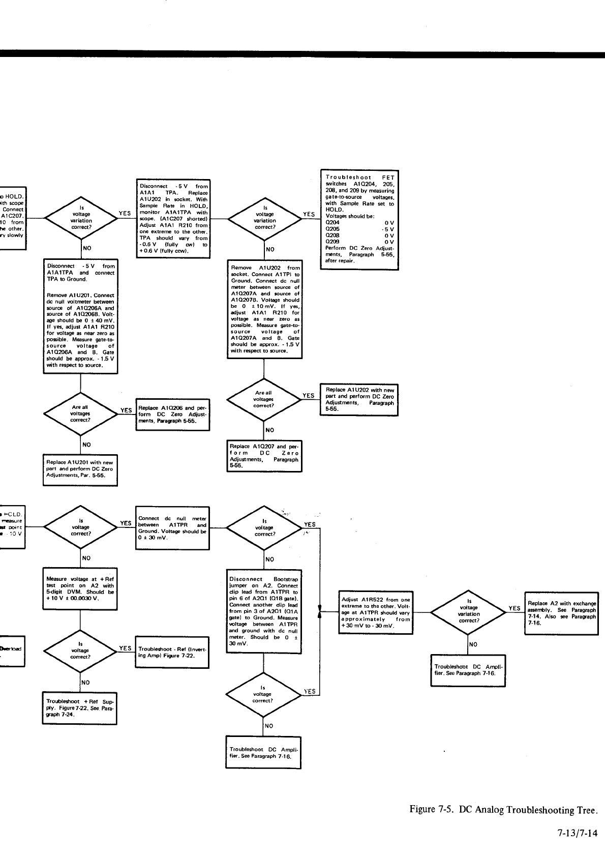
O HOLD,
ith @p€
Conned
A1c.207.
l0 from
h€ orher.
Trouble.hoor FET
sitchB A10204, 205,
2G, and 209 by m€suring
gate-tosur@ voltages,
with Sample Rate set to
HOLD.
Volbg6 3hould be:
o2or 0 v
0205 -5
V
0208 0 v
ozx, ov
Perfo.m DC Zero Adjust-
runta, Parag6ph 555,
after repair.
AlAl TPA. Repla@
A1U2O2 in ocks. Wirh
Sample Rae in HOLD,
monitor AiAITPA with
sp€. (41C207 shortedl
Adju$ AlAl R210
extrere to the othor.
TPA should 6ry
-
0.6 V {fully dl b
+
0.6 V (fully cil).
Db@nnet -5V lrom
A'lA1TPA and @nned
TPA to Ground,
Remve 41U2O1. Conned
dc null wltmter b*wen
eur@ of 41O206A and
surce of AIO2OOB. Volt-
age should be 0 t 40 mV.
lf y6, adjus AlAl R210
for bltage at n@f zslo as
posible. M€aure gate-to-
source voltage of
AlOZ)GA end B. Gate
shoold b€ approx. -1.5V
with rspoct to $wce.
Remove A1U2O2 from
ocket. Connect AITP| to
Ground. Conn@t dc null
ffier betreen sure of
A1O2O7A.nd sure of
A1O2O7B. Volbge ihould
be O t l0 mV. lf y6,
adiüs AlAt R210 for
rclbgp aa n€r z€ro as
rcsible. M6sure gate-b-
source voltage of
A1O2OTA and g. Gate
should b€ approx. - 1.5 V
with r6rd to sure.
Repla@ AlU2O2 with ns
p6rt and pefform Dc zerc
Adiusmnts, Parag6ph
Redae A1O2O7 and per-
torm DC Zero
Adiusrcnß, ParagEph
5€s.
Replee AlU20l with new
part and pertorm DC Zero
Adiu*tunts, Pe. 565,
F Eint
. i0
v
Connet dc null mt6
bdwen A'ITPR and
Grourd. Volbge should be
0r30mV.
tl/leere 6lbge at + Ref
Bt Fint on A2 with
+digit DVM. Should be
+ t0 v t m.oo30 v.
Diiconnsct B@ffi6o
iump€r on A2. Conned
led from A1TPR to
6 oI A2O1 (O1A
s.te).
Conned anothff dip le6d
trom pin 3 of A2Ol (OtA
to Ground. Measure
berw@n A1 TPR
and g.ound with dc null
Mer. Should be 0 1
30 mV.
Adiust AlR522 from om
extreme to the other. Volt-
a!ß at AITPR rholld 6ry
approximately from
+ 30,mV b - g) mV.
asritly. Sa Pa.agEph
?-14. Al$ se PaEgraph
7-16.
Troubletr@t - Ret ilnffi-
ing Ampl Figre 7-22.
Troublerhoot DC Ampli.
tier. S€e
Paragraph
7-16.
Tror6le*r@t + Ret Sutr
ply. FigureT-22. Se PaE"
gtzpl\ 7
-24.
Troubleshoot DC Amdi-
tift. Sa PaEgräph 7-l 6.
Figure
7-5. DC Analog
Troubleshooting
Tree.
7-r317-14
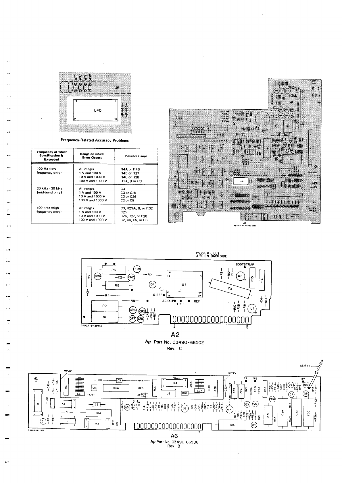
,i: : :!-.:=:
)l:B :.
.' :,}:r*,,3'3:,.
[:üqüffi J5
u40l
Frequency-Related
Accuracy Problems
1ü::ö
si:st
ö.:iil
Fr.quency at which
Spcifi6lion is
Exc6dsd
RangE od which
Error Occurs Posible CauP
1OO Hz (low
frequency onlyl
All ran96
1
Vand IOOV
10 V and 1OO0 V
10O V and 1 000 V
R4A or R4B
R4B or R27
R4C or R28
R1A,8
or R3
20 kHz
-
30 kHz
{midband
only} All ranges
-
lVand1O0V
lOVand1OOOV
100 V and 1OOO V
C3 or C25
C3 or C26
C2 or C5
'100
kHz (high
{r.equency only} All ranges
1 Vand
1O0V
10
V
and 10OO V
IOO V and 1OOO V
C3, R29A, B, or R32
C26,C27,or
C28
C2, C4,
C5, or C6
c5.c6 a Lt.L2
ARE ON BACK SIDE
acoutrt a a-REF
+REF
hP Pott
No.
O349O-66502
Rev. C
,^,,:z)
o(o8)Föö (c
ra'" G
VI
I 'T-_l I
tnt tl
l'l
-
ll
llt
"I
J +_.JL
liffml''*i,l++*
'il++ | 1"6;
lrr^,^V
z\ Q9e, r-L--.
(u4J',,.,',,r1
|
-Eet+r+l
I'l+
c,6 f ol LfT
Irl
TN
| | -fr _ RrB___-c r-t l.r-1 ,l , fl-
ll =:E llll x4 llP:-E
lFl lrl- rr)--+
l['l +tr l.:l---.] R4a F-cz:- lll .u-r-.-----U Y .+,
| | :1- tJ lczzl
L--l I
ce | -co- =FÄl-
LJ !,. I Ec--
A6
hp Porr
No.
03490-66506
Rev I
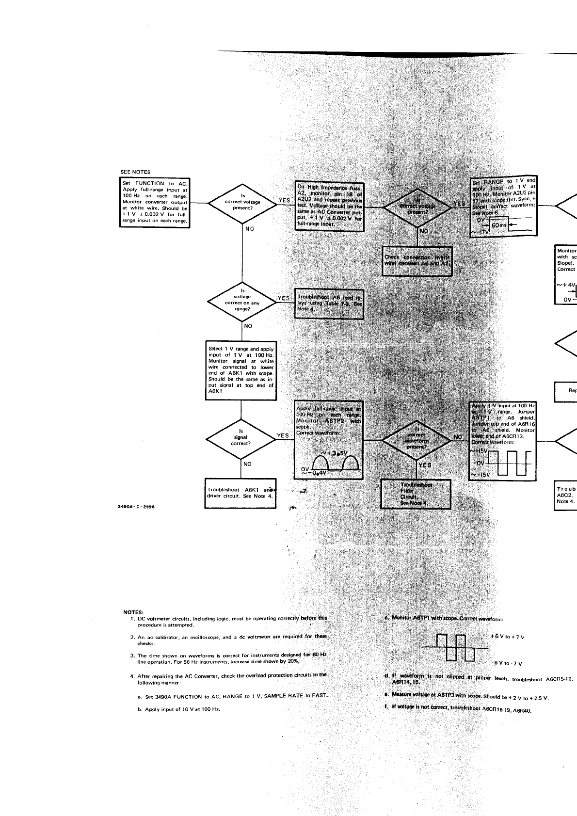
SEE
NOTES
14904- c - 299A
3. The time shmn on waveforms is @r(ect for instruments designd foa 4.t4,:'
|ineoFration.For5oHzinstruments,incr€setimeshownby20%;
a. st $wA tsuNu I tuN ro Au,
b. Aply input of 10 V ar 100
Hz.
6Vto-7V
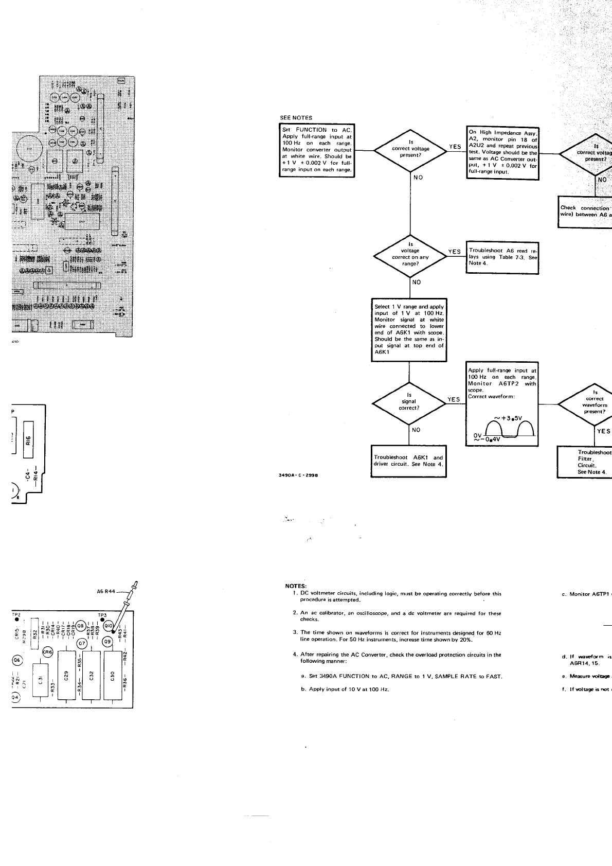
, , iliii#;, ,i
;_r;;rs6tl
I f4Fiü!t{#l tttta
'vvv::ttt:
*iii,tif6l:..it@i6
tigl:,ii
.14,iä,
:*,rii'.i
"-*"rti,"r";
preent?
'_:
i
Check conriection'
wire) b۟en 46 at
Troubl6h@t
Filter.
Circuit.
See Note
4.
NO
ä
i
ffi ##'.r,.rllt{i+WQrr,..',,:,.
;
:r,,,,tjjf*-ilsss8iiii..r,
.
.ffi,
t,?rS
lI*
NOTES:
1. DC vollmeter circuits,
including
logic, must be oFraling correctly
betore this
procedure
is
attempted.
2. An ac €librator, an oscillos@F, and a dc voltmeter are required for these
cnecKs.
3. The time shown on waveforms is @rrect for instruments designed fd 60 Hz
line operation.
For
50 Hz instruments, incrEse time shown by 20%.
4. Afler repairing the AC Converter. check the owrload protedion circuits in the
following mnner:
a. Set 34904 FUNCTION to AC, RANGE ro 1 V, SAMPLE RATE ro FAST,
b. Apply inpur of'10 V at 100
Hz.
c. Moniroi A6TP1
r
d. lf Fw{sm ;s
A6Rt4, t5.
e. M6ue rclEg! i
f. lf 6lbgabrcr(
Ser FUNCTION ro AC.
Apply Iull,range input at
100 H2 on each range.
Monitor convener output
at white wire. Should be
+1V 10.002Vforfull-
ßnge Input on each
range,
High lmpedane Assy.
montto. pin 18 ol
as
AC Converter
out-
+l v r0.002v
for
ange input.
Troubleshoot A6 reed re.
Select 1 V range and apply
input ol 1 V at 100H2.
Monilor iignal at white
wire connected to lower
end of A6Kl with s@pe.
Should be the sme as in-
put signal at top end of
A6K1
Apply Iull-range inpul al
10OHz on @ch range
nitor A6TP2
g,#h
Troubleshoot 46Kl and
driver circuil. See Note 4.
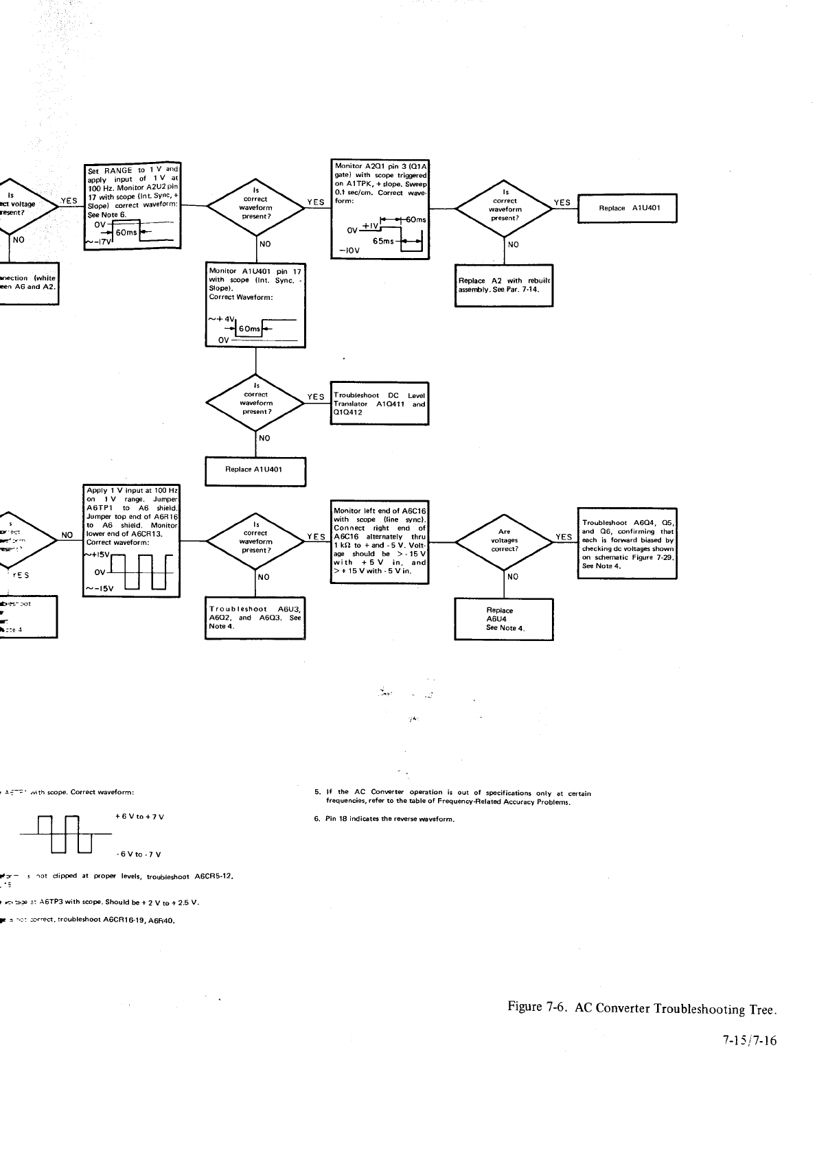
Monitor A2Ol pin 3 lO
t7 with scope
(lnt.
SYnc'
ov
1--t==-
-'l 6oms
l.-
-r7vl
Monitor A1U401 pin 17
with s@pe (lnt. Sync.
Slope).
Correct Wavelorm:
-* 4V1
--l OomsF-
assdüly. Se Par. 7-14.
Troubleshoot DC
Translaror A'1O411
ls\
E volbge
t€gt?
NO
retion (white
En A6 and 42.
.
iE S
b*-$r I
,l
-l
| :a-:' dth s@F. Corred Mveform: 5. lf the AC Conwrter operation is out of specitications only at certain
frequencies, refer to the bble of Frequency-Related Accuaacy problems.
6. Pin 18 indi6t6 ths rewrse &velorm-
+6Vto+7V
'6Vto-7v
t-- ! io! dipped ar prope levels,
troubteshoor
A6CB5-12,
.'=
I r,3- :: A6TP3 wirh 3@pe-
Should
be + 2 V to + 2.5
V.
F i -.:: s6, troubleshoot
A6CR16-.19,
A6R4O.
Figure
7-6. AC Converter
Troubleshootins
Tree.
Apply 1 V input at 100
on 1V range. Jumper
AOTPI to 46 shield
Jumper top end of A6R
to A6 shield. Monitor
lower end of AGCRl 3.
Correct waveform:
Monitor left end ot A6C
with scope (line sync)
Connect right end ol
I kf,l to + and ,5 V. Volt.
age should be > - 15
with +5V in, a
>+15Vwith-5Vin-
Troublesh@t 4604, 05,
and 06. @nfirming that
@ch is tomard biased by
checking dc wltag6 shown
on schemlic Figwe 7-29.
S@ Note 4.
Tro ub leshoot 46U3,
A602, and A603. Se
Note 4.
7-1s
17-t6

,r'ji
::a
ta$l -
o-ata
;.ä.,
tgtEa:
l. DC dril- d..Grttt, lr.fda,|3 hCc. |ür b ogmiig ffity b.tor.
.tütgi||tl$Fdn
t. Aß ddüCoo9.., r 0 tlrt;lt wath anD{r r.d3re. o, tolootn,.r I
orwrrndrüd ItdadEdc.
3. fh. üD Jwr d ilrdo.E - ffi lü i.il.ufErt! O|i$d lq d, Hr
fm op-rtion. Fd 50 tlr iü|rmB, iEe ünr bv 2O*.
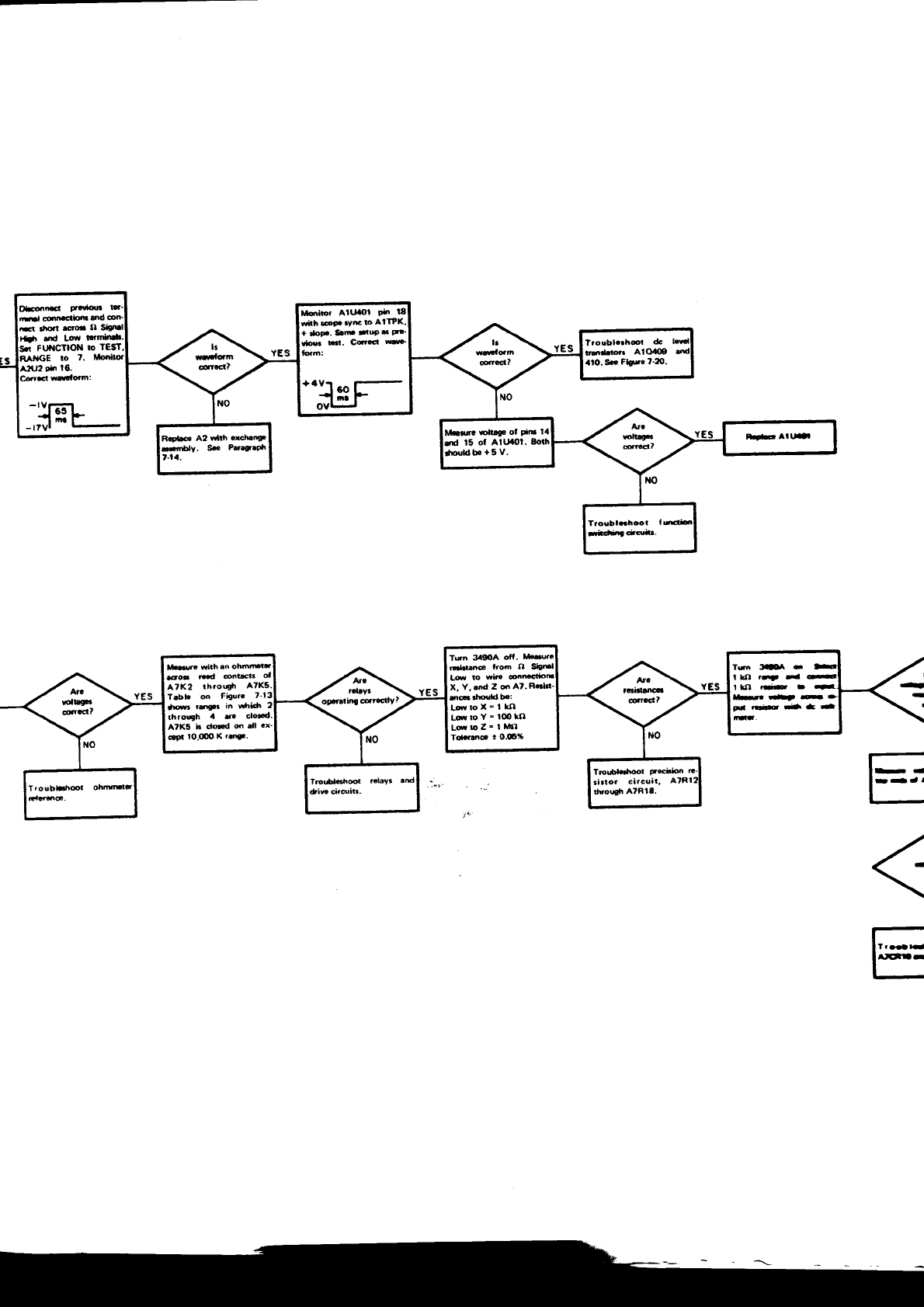
Ficlinud@D
G $dr.@{t
llar ..td Ld
S.r FiI{CTION b TEST
+ 5F. Elm tlup a F?
lr-s Fhtgo of ]i6 14
rd 15 ot Alt}|{rt.
JFu'ldbo+5V.
X. Y. rnd Z 6 Ar. Raln'
ü6 .hould bar
LdloX=1 kn
LqtoY-tmtO
LqbZ- | lÄl
Tdtilc I 0.699
Tn t||u c
lm r.tt -
llo .-E D
T.ble d Figut. 7'l
öort targ[ in whiS
throügh 4 & dotd
A7K5 k do..d o dl .x'
€pr tO,ülO X rüaa.
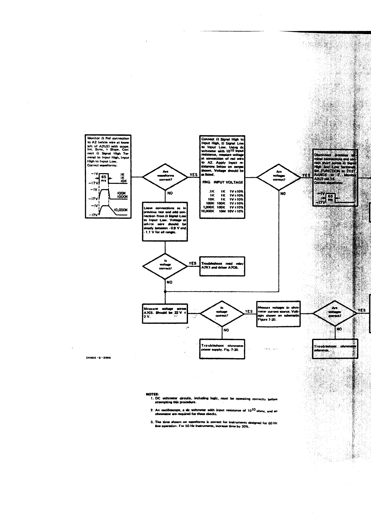
,r'ji
::a
ta$l -
o-ata
;.ä.,
tgtEa:
l. DC dril- d..Grttt, lr.fda,|3 hCc. |ür b ogmiig ffity b.tor.
.tütgi||tl$Fdn
t. Aß ddüCoo9.., r 0 tlrt;lt wath anD{r r.d3re. o, tolootn,.r I
orwrrndrüd ItdadEdc.
3. fh. üD Jwr d ilrdo.E - ffi lü i.il.ufErt! O|i$d lq d, Hr
fm op-rtion. Fd 50 tlr iü|rmB, iEe ünr bv 2O*.
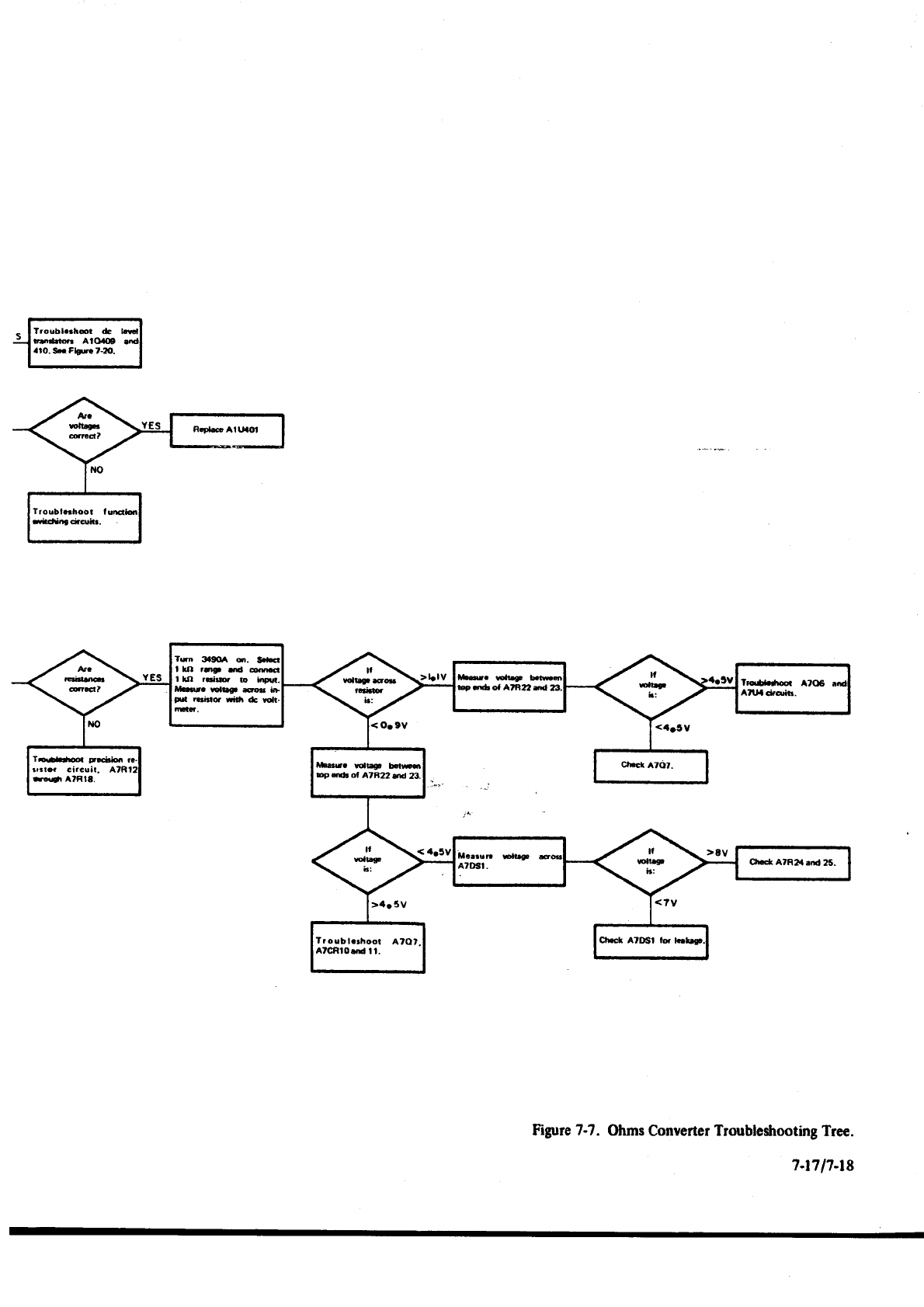
Troubl..hot &
ü5rhoß AIO{19
4tO. S... Flgm ,-2O.
Tm 3a9OA o.
I Ul rrgr f,rd
1 t$ r.ris b
lß8ü. wlESr bdFs
Dp qrb of A7R22ryd 23.
Troubl..hoor A7Ot.
A?CRIOüa ll.
Figure 7-7. Ohms
Converter Troubleshooting
Tre€.
7-r7l7-r8
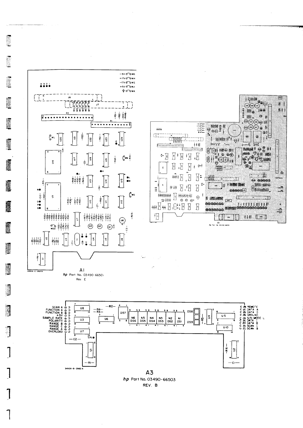
- 5v (ti! wc
+ t7v
(t-u w H
4 ! 2 | -r?vd-uwr
aaaa +5V6-UWJ
f obwx
r-a;---- --i-a-\
lt J8 ll
i I v .__!)-)---7:-t-a--a-ä6 --?a-r
| | rI-rr
t_iub_s!!h " " jl
<ooo'ä;--
=;]ill
aa
a a
a a a a aa
a o a a a
aääil5
| | ri
,-..E
:E
*
.E
{E
,"E
Tt"
l.l
l-l
tl
.K
fi
l5l
,tl
ß*i
"TT
l;l
tl
!|.J-
T-r
I lat
lil o"
t-l
D
trs
1-1" \)
tl
tryl
t-l
:L,l-
aJ
rrrr r'l--T
3;x3 3 l-l
cEcE t I il
",trl-l
"fT
l5l
tl
{u8)
V
'rl'
II
t'l
rtl,
++f++++++++
-L ii!*'J
woo
ffiii
"n "rT
iiJt*
lEl
+*tJ
I'l
rrrrsl_l
r||r
.LJ
N'
'l
o9
oa
P'
aa
AI
tp Port No.
O349O,6650r
Rev E
ä
=
l
IA3
hp Port
No.
0349O-66503
REV,
B
1
I
e*-ä
ä,ii
(,
*i ru*nir+lU
l.'i'...a :i :.:..
ü..?r ,:..,:
#l'[s]ri:ieo,e*l
$i'iäleffi
G,E;ff#::ri.
"';:lil
E'ä'ä'ä"a
's,*,,**
= tt=*-*.-.---:
,,,,uf,.,,;8,0:;HE
H ffii1****i*id t
"[J'+**e*
"rö
l"'lffio"lPl ,.
L-+lJ:..lJ!"1#.1J,..
l#1 l#
|
,,,lHlf
^
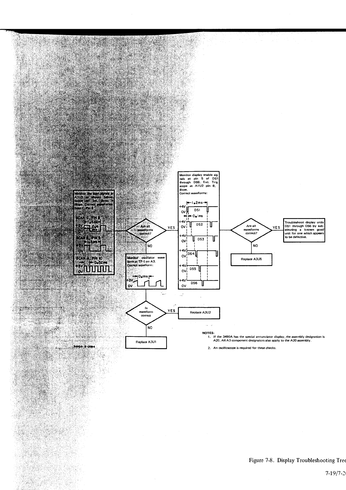
NOTES:
1. ll rhe 34904 has the speial annunciator display, the a$embly dBignation is
A20. All A3 @mponent dBignators alp apply to the A20 6semt lv.
2. An Gcillospe is required for rh6e checks.
Figure 7-8. Display
Troubleshooting
Tree
7-t9lt-:l
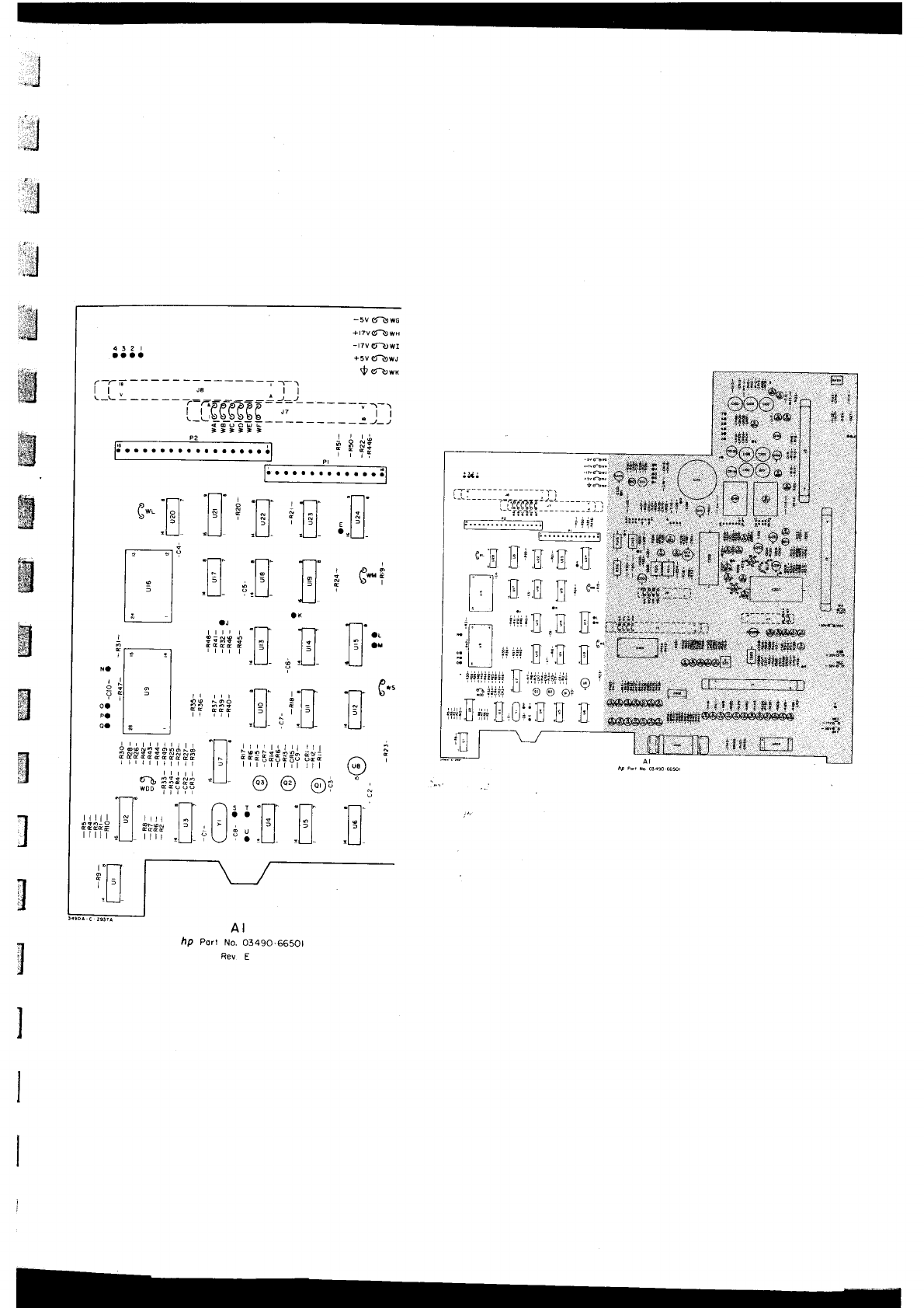
3
H
jd
ffi
ffi
ffi
ffi
ffi
g
ä
ä
l
i
I
I
a
a
a a a a a a
aa a a
o a a a
AI
tlp Port No.
03490,66501
Rev E
.-.
'n^ rT_l^ Il
lsl
iltl ,lll
=LJ. 'L--l ',Lj-
Na
9
oa
P'
oa
i'Ta---
-- -;------ it
tl'-'- --- ' '
t -L,r_!-*!i _ _,,_ - _ _ - - j - l
r.r""..........{ i ti;
r.'.''......1
" n Tll'R n Tl'
t- l3 ßt i :l i t:l trl
,lJ .lJ ,lil Il :.ü
[El* !#W.' ü::iliiff"
::= @@@@@
lil9**effi!+-
ti f*#i**$S
r- fr-.- -t--ln
@@ee€6e* iiif itiFtiils
omo i$##l@@@@@o@sso
-
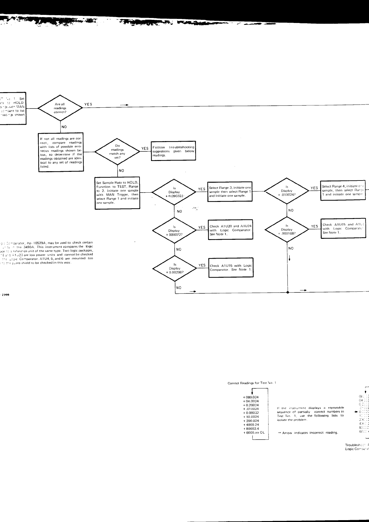
::.-Joc ?lfo-l
? :r 1llsalqnora
,.-,lg oulpeai ]carloJu! salFlpur Morrvr_
a .t:t
:: :,ta uälqord aql alelosl
::: _t or slsrl bulMolloJ aL]r asn 'l oN ls31
:.-- -, 0 + u! slaqunu lJa,oc ^llerued lo af,uänG
::: .
l etqeleadar e s^eldsrp luaunrlsL' aqr ll
l,;00,.
t'20004 +
va ooov +
bzo ooz
+
tz00 0l
+
2t060 0
+
tZ00
l0 +
vzooz o
+
t t: !
:::
r0
I
J ?Zo0
r0 +
tzo oB0
+
It
L o\ rsal rot s6urpPau
rrarro:)
L aloN €as rorB
)r6o-t qlrM 9lnlv
' | aloN aas
'rolerdu03 rr60_l qlrM
tznlv pue oznLV )iraq:)
' I aroN aas
,
rtereduoJ J160
l qllM
:itv pus 9tnlv )3aqc
-aldues
3uo
ale!l!ul pue L
a6ueu tralas
uaqt 'ra66tra NVW ql!M
3ldu6 €uo alelllrrl z ol
a6ueu'asfl ol uollcunl
'c_l
oH or aleu aldues ras
'aldus auo arell!ul
pus
! a6ueu
]calas
uaq] aldu6
auo
elerlrur
't 36ueu
rrälas
. du6 auo alerrlul Pue I
:aJPU rf,stas
0aqr'alouB
:-,o alcrlrur't 36ueU lcälaS
-parsll
sburpeäJ lo las ^ue ol l6q
-uap! are peurelqo s6u!peeJ
aq] ]r aurulelap ol'Mol
-€q uMor]s s6ulpeal snoau
-orr€ alqrssod ]o slsll qlrM
sbulpear aieduoc 'lcal
roc are s6ulpear lle rou ll
Molaq ua^!6 suo!rsa66ns
6urtooqsalqnoi] Mollol
'^eM slql ur palJaqc aq ol plarqs
orE_: :-: :- ;
ool psluno0 are gpue'g'tn!v rolerduol rr::- :-:
pa)3aqr aq ]ouuF pue slrun iaMod Mol are ea. l: : -: : ,
'\abplrhlri6oloMl ad^r
duP\aulrollJ.ar.:,_:-,' -':--
f,t6ol eqlssreduocluaunrrsur slql v06tt :ur - !: -
urPrral lldqr ol Fsr oq ^PU v6z9or dq io:c - _ : :
lsll
o:;r--:l
NVri :!.. i- tr
o-1ots.:;:.
F: ru*rffifc_ f*tEv:
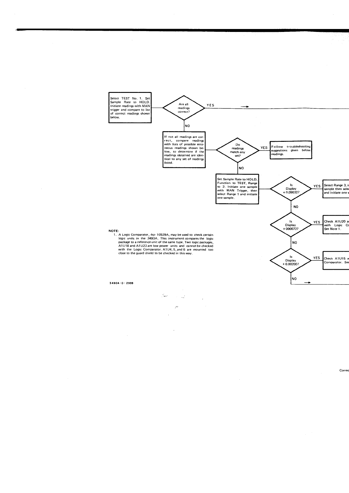
Select TEST No. L Set
Sample Rate to HOLD.
Iniriare
readings
with MAN
trigger and compare to list
ot @rrect readings sh@n
ll not all readings are cor-
recl, compare readings
with lists of possible erro-
neous readings shown be-
low, to determine il the
readings obtained are iden-
tiel to any set ol readingE
listed.
Ser
Sample Rare
to HOLD,
Function to TEST. Flange
to 2. Iniriate one smple
with MAN Trigger, rhen
elect Range
1 and initiate
one $mple,
YES Select Range 3, ir
gmple then sele(
and
initiate one s
A Logic ComFrator, -hp- 105294, roy be used to check certain
loqic units in rhe 34904. This instrument@mparesthe logic
Fckage 1o a reterence unit of the same tvf. Two logic Fckages,
AlU18and A1U23are low power units and €nnotbe checked
with the Logic ComFrator.A1U4,5,and6 are mounted ioo
close to rhe guard shield ro be checked in this way.
!490A-0-2999
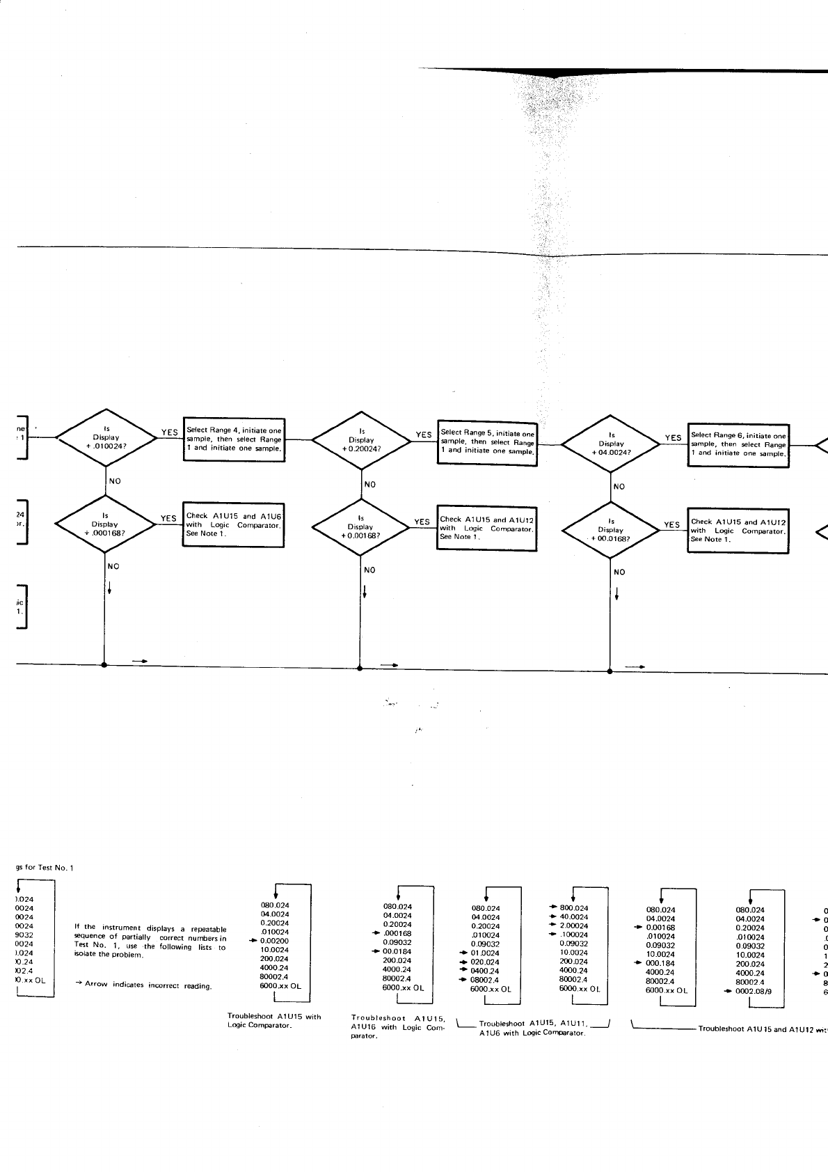
smple, then select Range
'l and initiate one smpte.
S€lect Range 6, initiate one
smple. then *lect Range
I and aniriare one €mple.
ls
Display
+ .oo01
68?
Check
AlU15 and A1U6
with Logic ComFrator.
See Note 1 -
Check A1U15
and
A1U12
with Logic ComFrator.
See Note 1 -
Check
AlUl5 and AtUt2
gs
{or Test No. 1
).o24
oo24
@24
oo24
9032
oo24
t.o24
n.24
n2.4
IxxOL
It the inslrument displays a repeabble
equene of partially correct numbers
in
T6t No. 1, use .the following lists to
rclate the problem.
+ Arrow indi€tes incorect reading.
o80.024
04.oo24
o.20024
.010024
+ 0.00200
10.oo24
200.o24
4000.24
80002.4
6o00.xx OL
Troubleshoot
AlUl5 wirh
Logic ComFrator-
080.024
04.oo24
o.20024
+.000168
0.09032
+ 00.0184
200.o24
4000.24
80002.4
6000.xx
O
L
o80.024
M.OO24
o20024
.o10024
0.09032
- ot .0024
- o20.o24
+ 0400
24
+ 08002.4
@oo.xx
OL
+ 800.024
+ 40.0024
+ 2.OOO24
+.100024
0.09032
10.0024
20/).o24
4000.24
8m02.4
080.024
04.oo24
r 0.00168
.0't0024
0.09032
10.0024
+ 000.184
4000.24
80002.4
@00.xx
OL
040.024
04.0024
o.20024
.010024
0.09032
10.oo24
200.o24
4000.24
80002.4
+ 0002.08/9
-o
o
.c
0
li
z
+0
&
T:!
li'r'lt'?lt;''.."it 3"t,1-
\- t'"oresh@r
Ar
ur5 a
I ut
1
J
*rutor. A I
U6 wilh Logic
Corcralor
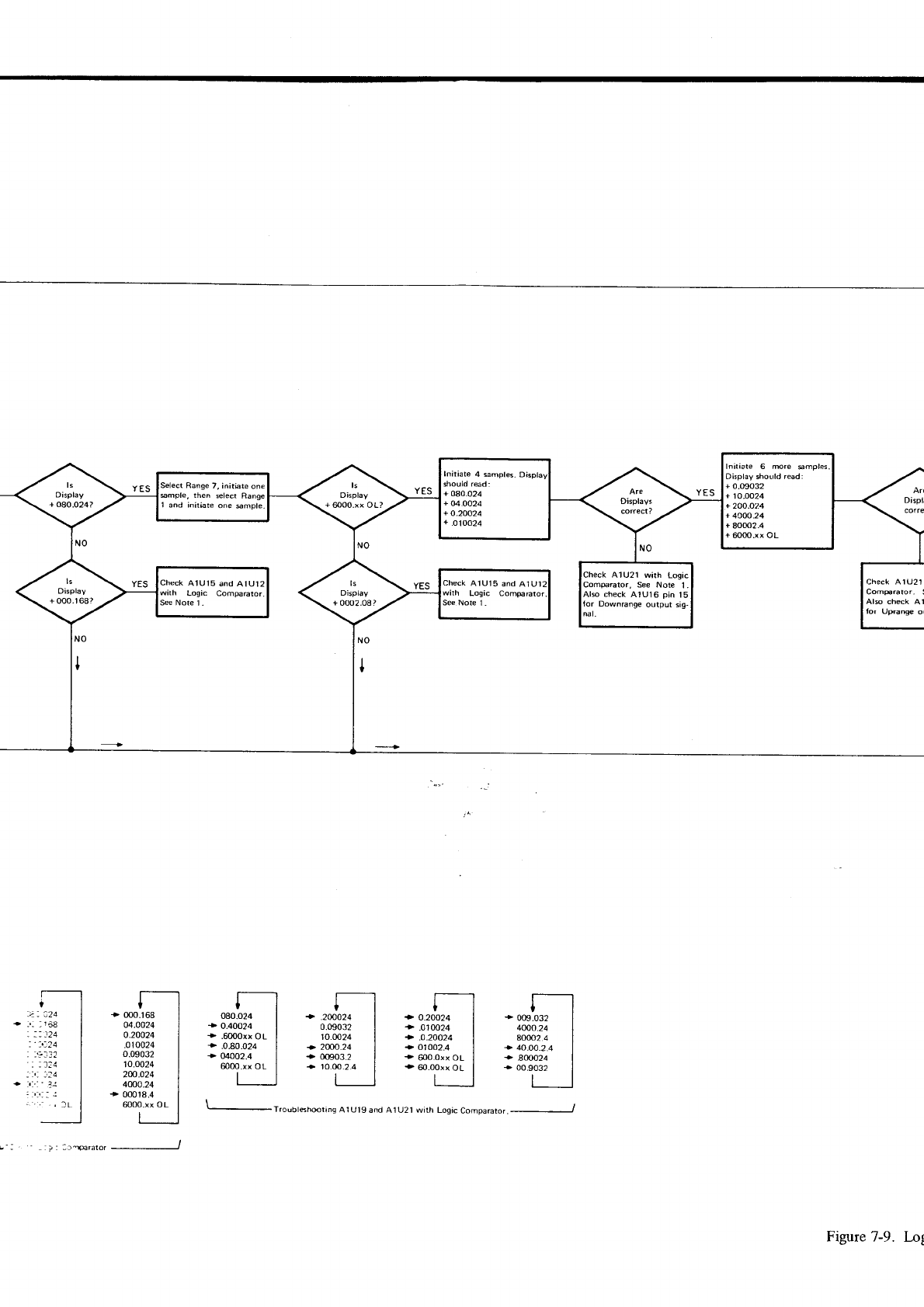
Displi
cotre
Check AlU21
ComFrator. S
tor Uprange or
+ 000.168
04.oo24
o20024
.o10024
0.09032
10.0024
200.024
4000.24
+ 00018,4
6000.xx OL
rl
080.024 |
+ 0.40024 |
+ .6OO0xx
OL I
+.0.80.024 I
+ 04002.4 |
600o.xx
ot I
f-l
+ .2ooo24 |
0.09032 |
r0.0o24 |
t 2cf,0.24 |
+ 00903.2 |
- 10.00.2.4 I
f-_l
+ o.2oo24 |
+.010024 |
+ .o.2oo24 |
+ 01002.4 I
+ 6o0.0xx OL I
+ 60.0oxx
OL I
n
+ ooe.032 |
4OOO.24 I
80002 4 I
+ 4o.oo.2.4 I
- 80oo24 |
- 00.s032
|
Initiate 6 mre smples.
Disploy should read:
+ 0.09032
+ 10.0024
+ 200.024
+ 400024
+ 80002.4
+ 6O0O.xx OL
ComFralor, See Note 1.
Also check A1U16 pin 15
Check
A1U15
and
A
with Logic ComFrator.
Se€ Note 1 .
41U15
and
AlUl
t: :rFrätor
\--Troubl6h@ting AlU19 and A1U2l with Logic
Comparator.-------J
Figure
7-9. Lop
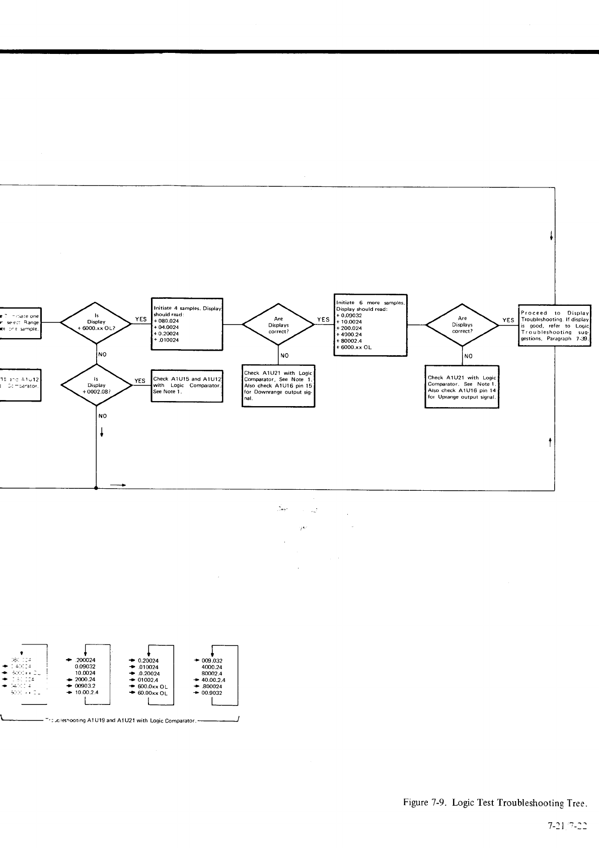
sai Range
Initiare
6 mre smples.
Display
sho(ld read:
+
0.09032
+
10.oo24
+
200.024
+
4000.24
+
80002.4
+
60O0.xx OL
Proceed lo Displa
Troubleshootang
suq-
Al U21 with Logic
check AlU16 pin 15
Check 41U21 with Logic
ComFrator. See Note l.
Also
check AlU16 pin 14
Ior Uprange ourput signal.
rl
+ 2OoO24 |
0.0s032 |
10.oo24 |
+ 2cf,[24 I
+ 00903.2 I
+ 10.00.2.4 |
f-_l
+ 00:).032 |
4ooo.24 |
80002.4 |
+ 40.00.2.4 |
+ 800024 |
+ oo.9o32 |
+ 020024
r.010024
+ .0.20024
+ 01002.4
- 600.0xx
OL
- @.00xx
OL
Figure
7-9. Logic Test Troubleshooting
Tree.
t-r65@ting A1 Ulg and 41U21 with Logic
Comparator.
----J
? al _ rr
I-- t
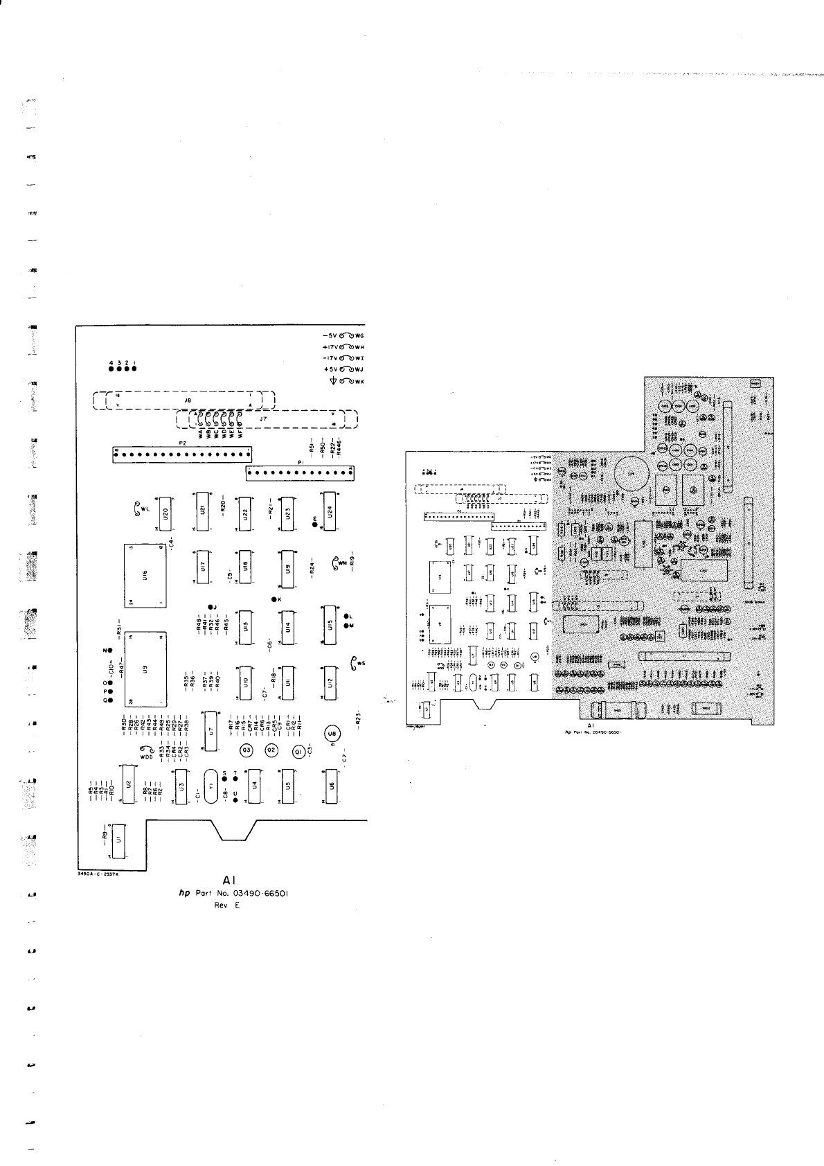
,+
{
iE
:..
:'
'|:
'.€
:.1:
.i
$
ii'!
+*
13
-tt
s,-.'
?:a
- 5v (t-Xr w6
+r7v(i-l)sn
-l7v 6\wr
4lz
I
aaaa +svd\,r-
f cnr wx
a-. ; - - - - - - - ---- -- -i a:-\
ll J8',
aaaaaaaaaa
.r---
1.
1-1" if-l' ||
Irl rlrl l{l
lrl I lrl €
l-l
,L-l ,L
l_ .'LJ-
"n' 'n il"
l'l sl.l lsl
!'J- :lJ .LJ_
.K
aJ
rr r1"l-l 1-t
3;s39 t-t t"l
iTrTT
l5l l5l
,L--i ,! :L--.1
?
T--l'
I Iar
lil r"
t-l
b
lrs
.n" D
l3l
tl
!u-
D tl
S"' IRI
trl
!U- E+
!a
,l
3p
il
oa
P'
oa
{ua I
'n"
lol
l-l
tl
it!
::
|
"f-I
T
l=l
=LJ
l,p Porr
No.
0349O-66501
Rev E
.,; ";t'E
"H
H-
n"fu----=t,'
.
'ä-'äfu
;'1
,,+,;1
r11
g*.,ffl#,'ffi gn*,#il
: l, | .Ll 'LJ .U ., ,.: . .EJgrr$i9{qgJ
: .+lrtfiltiji!::t
.:iili;i*iii
f..f
i,il;11,;,'.
6) i :
s.r:iiiir oooi ' !i,itldi##ig'Ll
Tl fin,,rr.n fl ,6es6@o9, iilti!iFii!r:
;,.':.fl
i.r"
.ll
,U,,.Ll
,ll tl €@CI6@@e#ffi
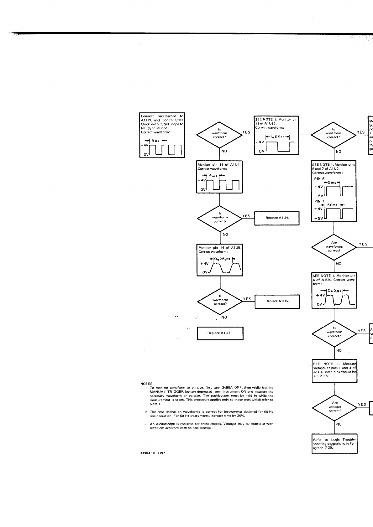
Connect oscillosope to
AlTPU and monitor State
Clock output. Set scope
to
Inr. Sync
+Slope.
Correct waveform:
SEE
NOTE
t. Monitor
11 ol AlUl2.
SE€ NOTE 1.
Monitor pins
and 7 of A1
U2.
l+5nsl
:;[-r
t'! .o." 1-
_,;ljl-
Monitor
pin 11 ol A1U4.
Monitor pin 14 oI A'lUs
Correct waveform:
E NOTE 1. Monitor pin
1U4. Both pins
should
Refer to Loqic Trouble-
shooting suggestions
in Par-
agraph
7-39.
M(
Sct
po
+i
YES
YES
YES
NOTES:
1. To monitor waveform or voltage, first turn 34904 OFF, then while holding
MANUAL TRIGGER button detressed,
turn instrument ON and m@sure the
necesgry waveform or voltage. The pushbutton must be held in while the
measurement
is bken- This procedure
applies oßly to those tests which refer to
Note 1
.
2. The time shown on waveforms is correct
for instruments designed lor 60 Hz
line operation.
For 50 Hz instruments,
increase time by 20%.
3- An oscilloscope
is required {or these checks. Voltages
ruv be m@sured
with
sufJicient
accuracv
wiih an
oscilloscope.
34904- 0
-
2$7
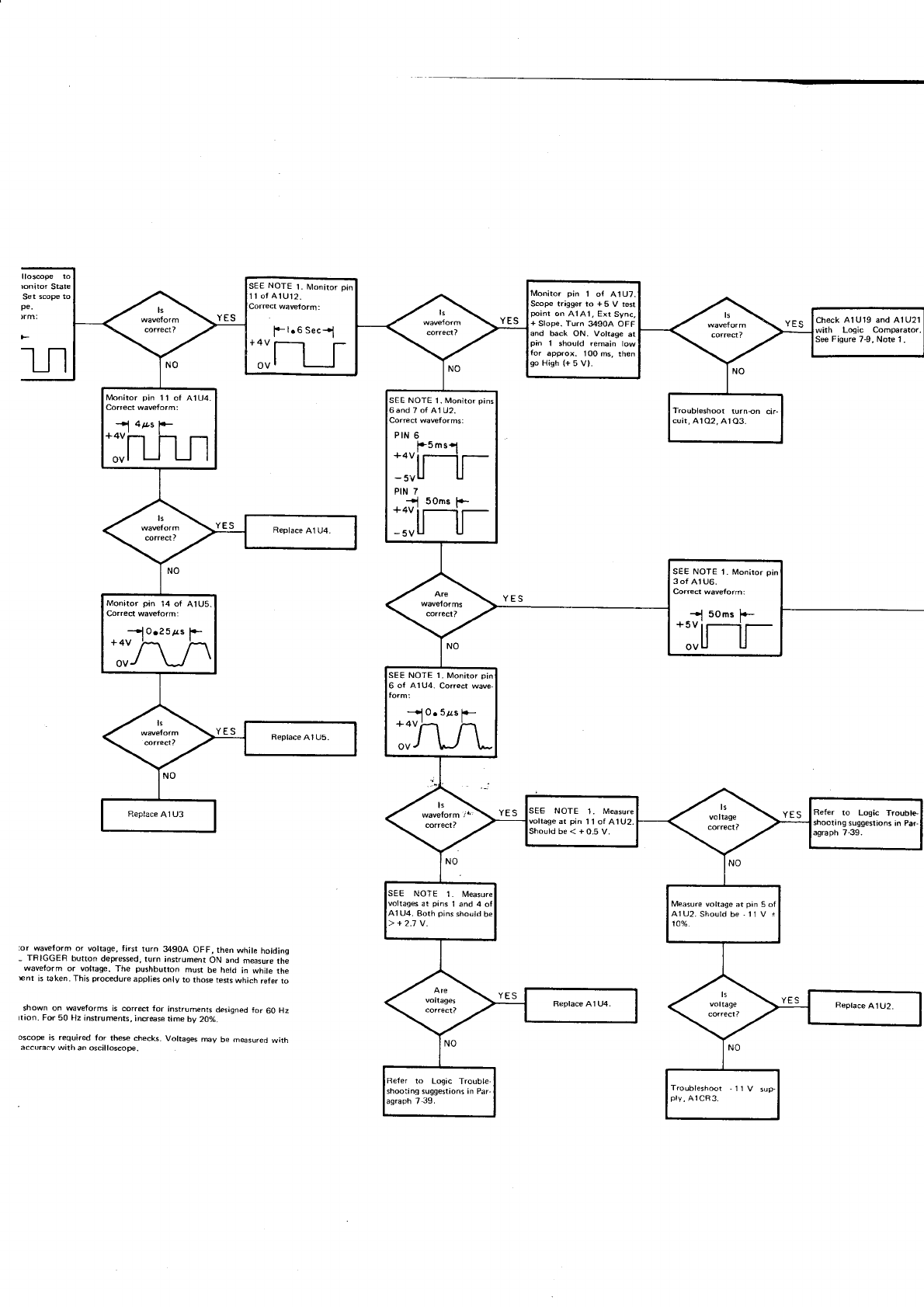
SEE
NOTE 1. Monitor
11ofAlUl2. pin 1 of Alt-J7.
tragger to +5 V lest
on A1 A1. Exr
Sync,
+ Slope. Turn 3490A OFF
back ON. Voltage at
I should remain low
approx. 10oms, then
so
Hish
(+
5 v).
A1 U19 and A1 U21
Figure
7€, Note 1.
SEE NOTE
1.
Monitor
pins
and
7 of A1 U2
';1;:-*"*-''
l+5
m
s-l
ltrl-
t'tj ,o." 1*
:lll-tl-
A't02,
A103.
SEE NOTE '1.
Monitor
3 of Al U6.
Correcl wave{orm:
I soms l.r-
I
-lu-lJ-
U.T:'"",'J"',l,:,t-:t
o t u u'
-+iO.254s
F
:1"/\/-\ E NOTE 1. Monitor
: NOTE 1. M€sure
ages at pins 1 and 4 oI
41 U4. Both pins
should
be
>+2.7V.
Measure
voltage at pin 5 of
41U2.
Should be'11 V r
to%.
Re{er to Logic Trouble-
shooting suggestions in PaL
agraph 7 39.
Troublesh@t ,11 V sur
ply,
AlCR3.
YES
YES
:or waveform or voltage, tirst turn 3490A OFF, then while holdinq
- TRIGGER tlutton depressed,
turn instrument
ON and measure
th!
wavetorm or volrage. The pushbution must be held in while the
€nl is taken. This
procedure
applies
only to those tests
which refer to
shown on Mveforms is corred tor instruments
designed
for 60 Hz
rtion. For 50 Hz instruments,
incr@se
time by 2O%.
oscop€ is required for these checks. Voltages mV be mesurecl with
accuracv with an oscillosco@.
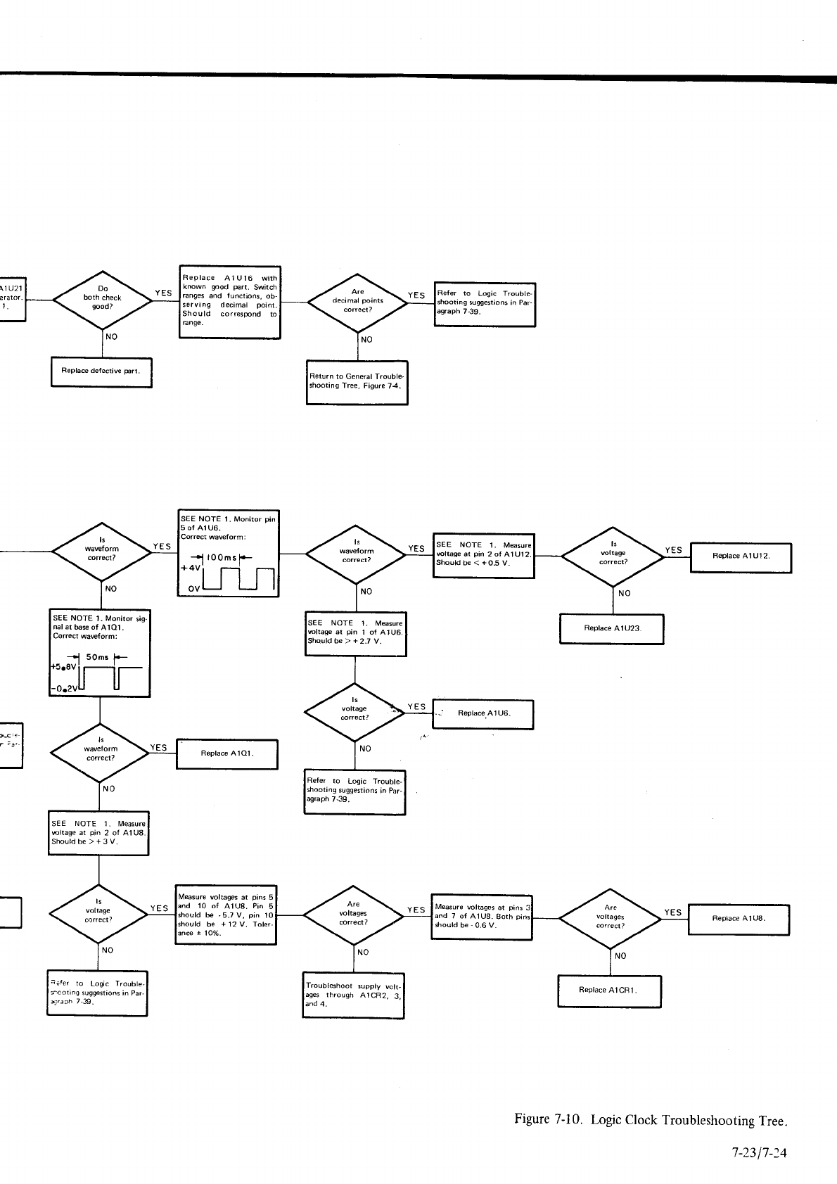
Replace AI U'16 wirh
known good Frt. Switch
cnges and lunctions, ob-
servang decimal poinl.
Should correspond to
Enge.
Return
to General Trouble-
shooting Tree,
Figure
7-4.
SEE NOTE 1. Monitor Din
SEE NOTE 1. M@sure
rcttage ar pin 2 ot A'U12.
Should b€ < + 0.5 V.
SEE NOTE '1.
Monitor iig-
nal at base of A101.
Corect wave{orm:
SEE NOTE 1. Measur€
rcltage ar pin 1 of A1u6.
Shquld be > + 2.7 V.
Reter to Logic Trouble-
shooting
suggestions
in Par-
agraph
7-39.
SEE NOTE 1. N/leasure
rcltage at pin 2 of 41u8.
Shouldbe>+3V.
Measure voltagB at pins 5
l0 of A1U8. Pin 5
should be.5.7V, pin l0
be + 12 V. Toler- and 7 o{ A1U8. Both pi
n.fer to Logic Trouble-
eooting suggestions
in Par
4.a3h 7-3g. throuqh A1CR2, 3, Replace
41CR1.
Figure
7-10. Logic Clock
Troubleshooting
Tree.
7-2317-)1
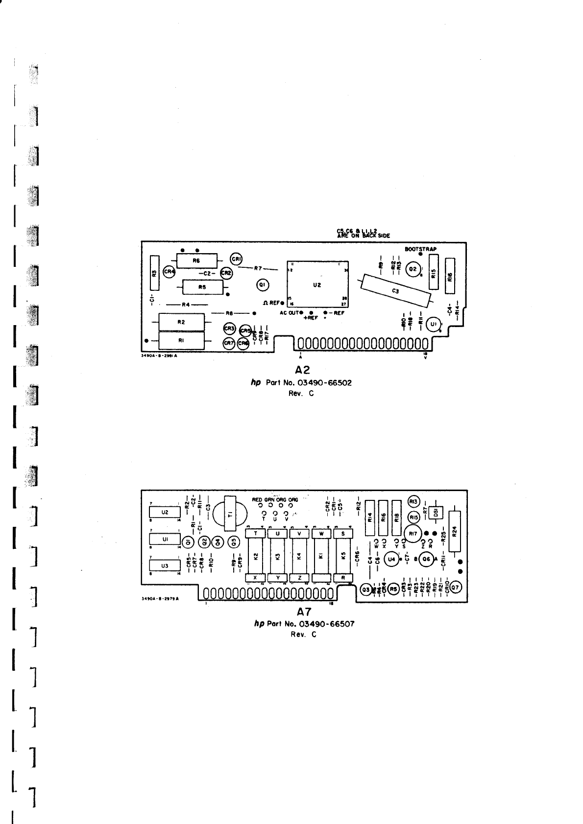
,j
ltr
*1
g
€
€
ffi
ä
,l
i*l
l
l
l
I
1
I
I
I
Ä,
hp eut No.0349O-565O2
Rev. C
S+ft$b!t}"oo.
E.E?*;f--"..--l
-&Ug
F -^o- ,r".r.l'" sl - - -Jt l\f- +1
+*
*o;
+EEE8+Hr,
llJtlfr.Il,l
++föi'ö+":
r@++@+f*****io
*++1,,{l-.,
*8o5Tr ts*
I ua
lr.tTf l;l ) ooo, ?Tr
:--- *t,\ / r u v
r---+ TT -r tHttttffi-
r__s_t@@@@
TIT-Ifi'rTf
''' ' "lcllell:ll'll!
I
-l$EB?
tE' rr rr rr rl
i-----
||' ' r'|+1HHHL
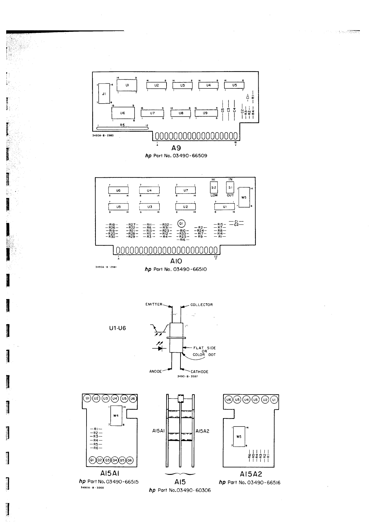
t-;l
,i
''1"-
Hffi-,'-r{{**-*l
\--------. t------- | I | | | | |
4Er48r48r40
|--ur--l f wl t u4-l f-C-l
t7tft7t7l
1:
oc
'49
hp Port No.
O349O-66509
ftftTl
lu6llu4llvTl
8K6i4814
t- us-l i- url I- u,-l
8t4B14814
0000000000000000000
/:\ -cr-
_RZ7_ _R'_ _RJZ_ \q, / _Rt5_ _C2_
-R22- -R6- -R3r- -R2- -R7-
-R2l- -Rr3- -Rzl- -RrO- -R24- -R8-
-R28- -R5- -Rr2- -R33- -Rr7- -Rl4-
-xzg- -K5- -X4- -nZ5- -Xv-
nn
l.'l l' l l---.l"
T -l',.
l
l-ll't '.
- Rt8-
- R26-
-R30-
Alo
hp Port
No. O349O-66510
COLLECTOR
U1.U6
,/t,
--ft- FLAT SIDE
OR
coLoR ooT
AI5AI
hp Port
No.0349O-665t5
3490A-6-5000
-
AICi
Ftv
hp Port
No.O349O-60306
AI5A2
hp eort
No.
03490-665t6
rf-----lr.
tt
tl
lw4 |
tl
rL_____l 8
-Rt-
-R2 -
-R3-
-R4 -
-R5-
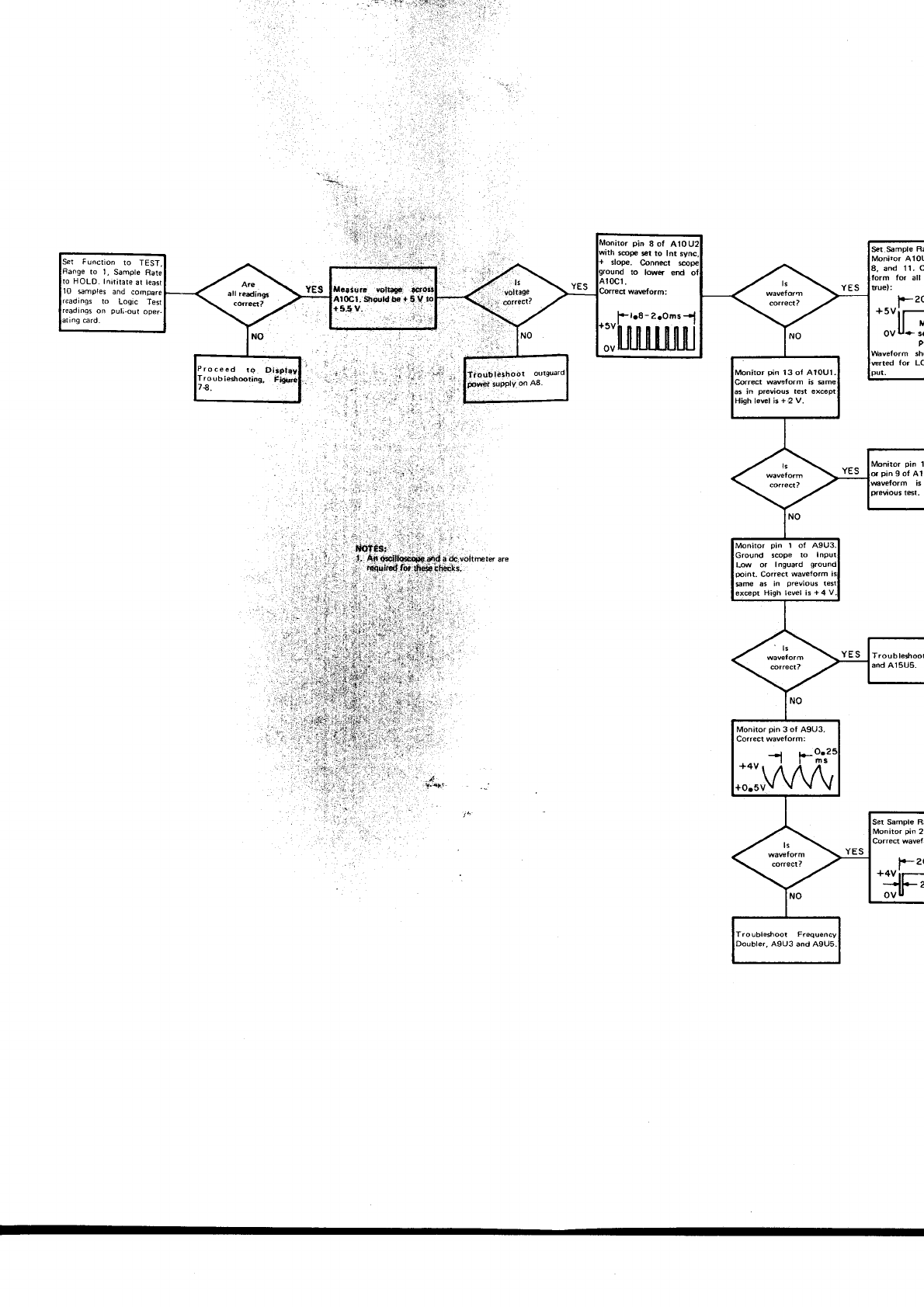
s@pe q to lnt sync,
At(fl.St@idbe+5V1.
t 5.S
v. :','
oin
13 of AlOUl
sme ar in previous tesl
except High lewl is + 4 V
Monitor
pin
3
of A9U3.
Correcl wave{orm:
_-] b_ o.2
| | ms
;.,,\AA&
Sample R.
AlOL
and 11.
C
for all
r2c
.:Jtl-
r
sh(
for LC
Troub leshoot
A I 5U5.
.#F
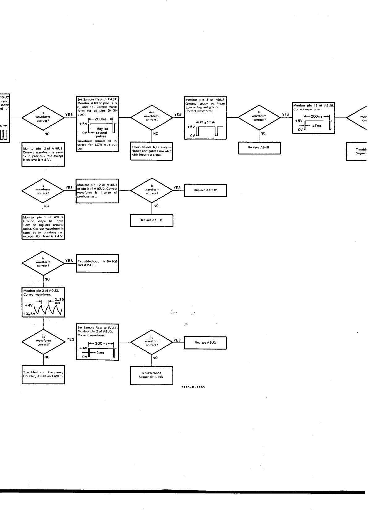
Sampte Rate to FAST
niror AIOUT pins 3;
and 11. Coiled wa
for all pins
I
l._ zooms-+l
.llj-*#ll
pulses
,m should be in
for LOW rrue out
.l[-:r
pin
13 of Aloul
pin 12 of Aloul
pin
I ot A10U2.
Correcr
Monitor
pin'l ol AgU3
Ground scope to Inpul
except High lewl is + 4 V
Troubleshoot A15A
;:,\^ÄÄ
Set Sample Rate to FAST
f+-
zoomsl
+4V i-J
Troubleshoot Frequency
Doubler, A9U3 and AgU5
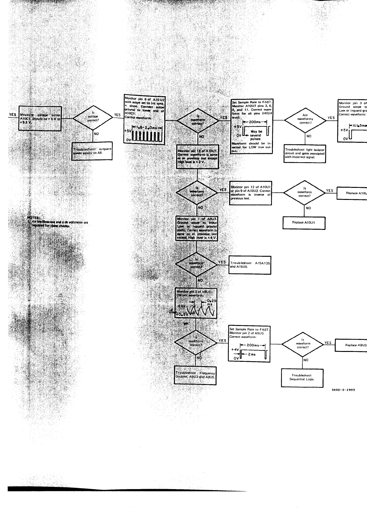
ti'1::i.'::"::
.1.1.1-:t.1
i ,,
.; t-.,''
pin 3 of
I r--
i't
:,i.
,:i.
::i
;;i
';=c -,.*-- .l[=-
or Inguard gro
Replace
AlOU
Replee
AgU3
..
.l-,"t '
.f,',
."
ea
i-,
.,:
H':-.
:'J.'l
YES
F.:;
t.:.
:_'.
!490-0-2995
-
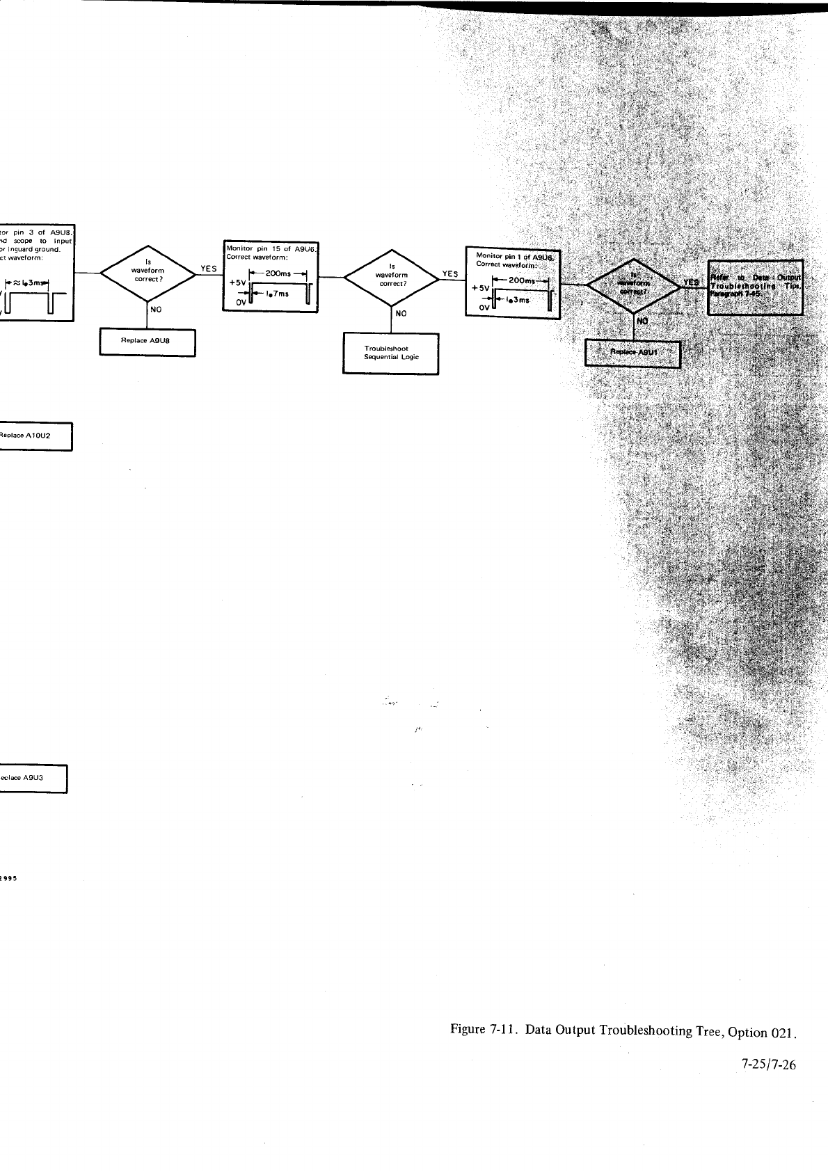
tor pin 3 of A9UB
{ s@pe to Inpul
). Inguard ground.
.
f= b3mtl
,[J-lr
Figure
7-1 1. Data
Output Troubleshooting
Tree,
Option 021.
7-2s17-26
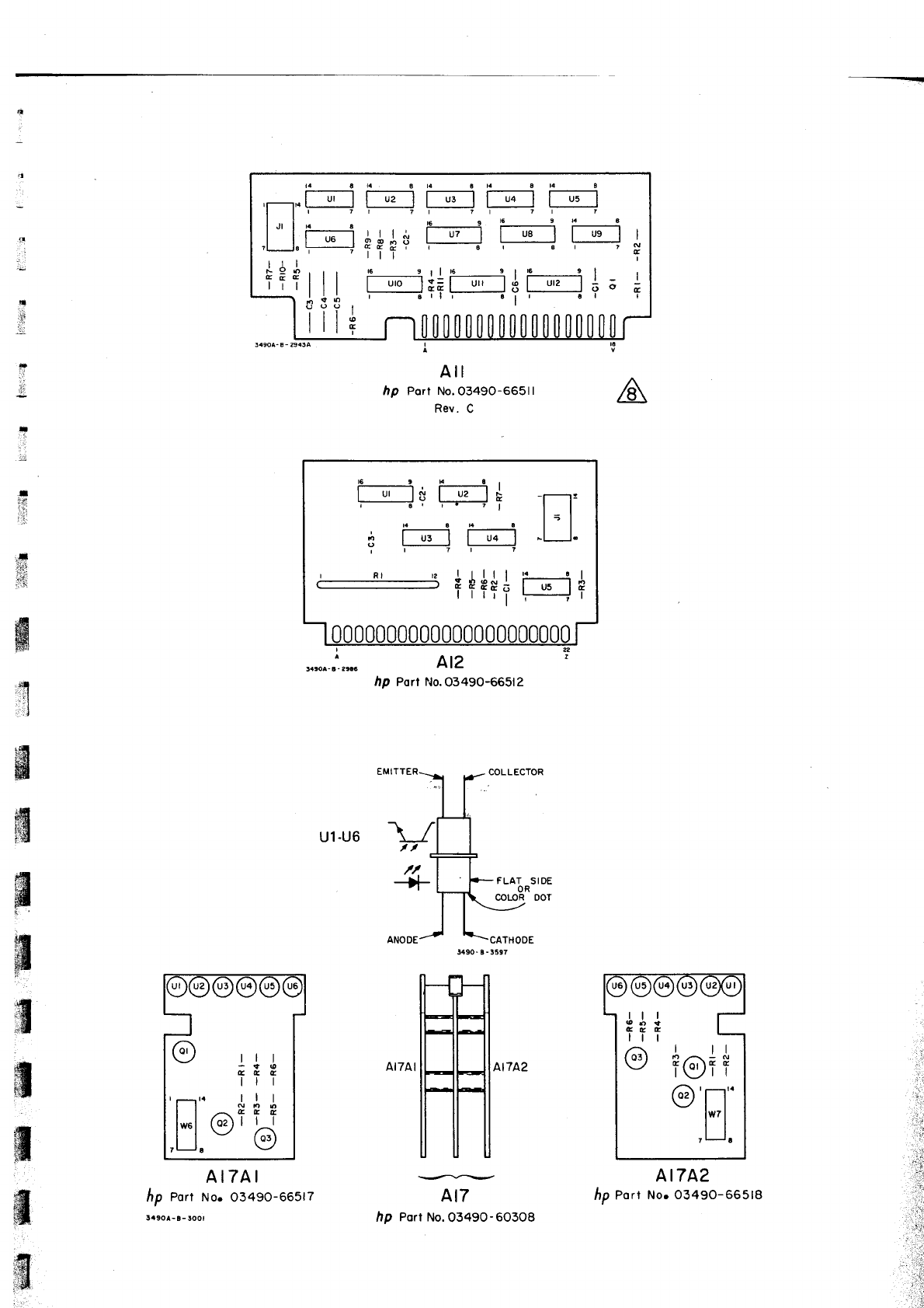
_
i.r
.l
aa
!
,X
i,
7
z
I
tn
-l
t'it'
::i.
.,ä
c
i€
#
ffi
q
.l
.:
a1
#
@
ffi
g
gig
fq
K
i.:
,ä
ä
fl
w
E
A
Arl
hp Port No.o349o-665t1
Rev.
C
U1.U6 +
!4$- B
-
!597
AITAI
hp Port
No.
03490-66517
\_
At7
hp Port
No.O349O-60308
At7 A2
hp Port
No. 03490-66518
i-,F---+r
|_-]|-;q I,
i. J?
ra8ßa
; [--r-u3--l l-- u4
I
? i------i :--------j
i-------g-----+ * +
t* I i!-u;i t
lllrl
Ht
re**
t,E:
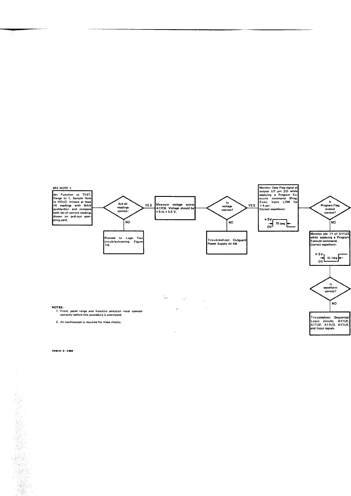
Exec. input LOW
) 5
psl.
pin ll of A1
tlu2, A't1u3, Arl
NOI€S :
1. Fron! pansl rang€ and function selection mu{ op€rate
@rectly before thir f@dure is attefifd
2. An osillo*or is
rquired for th6e chcks.
!4901- o
.
2s!
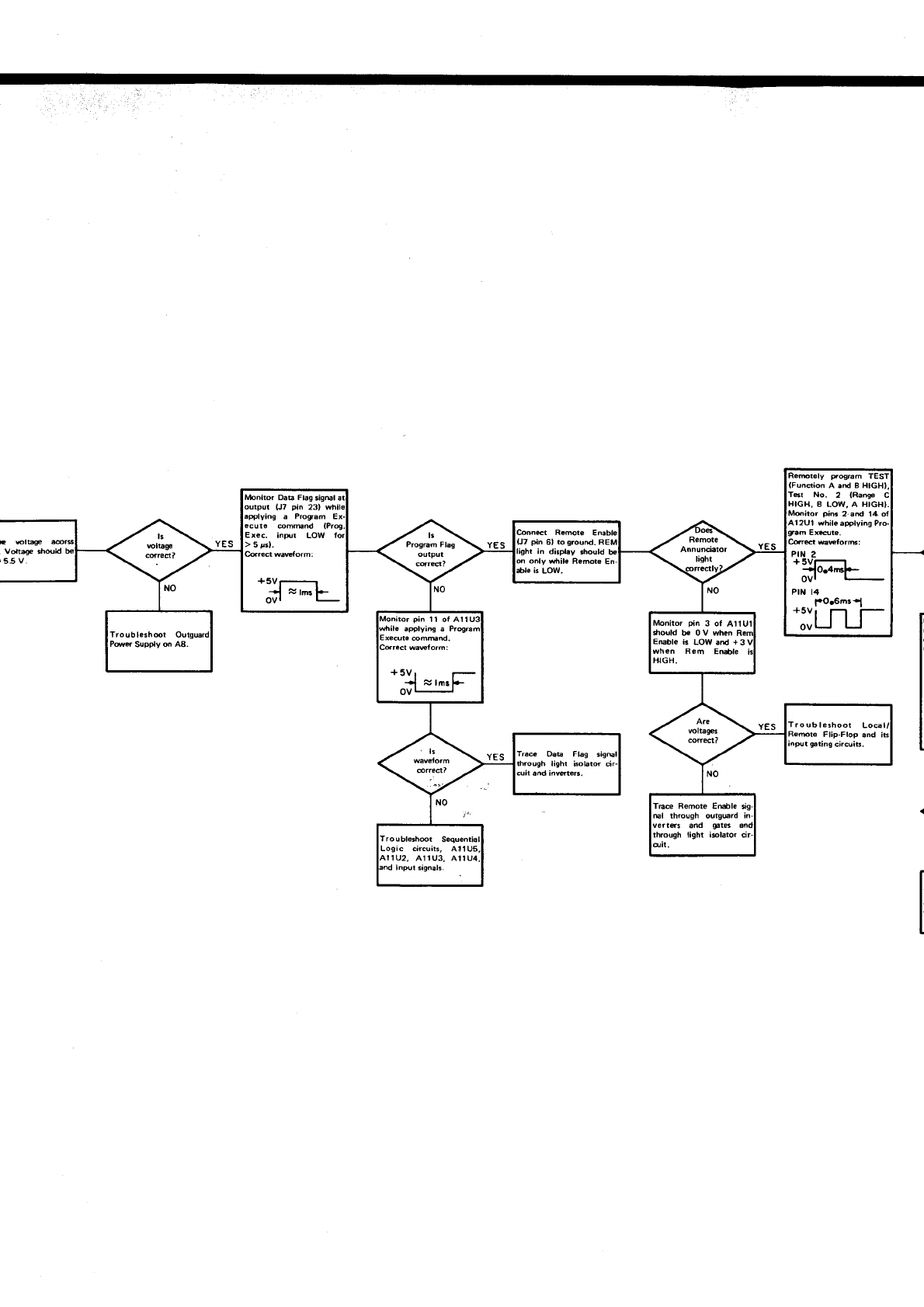
undionAendBHIGH)
No.2 {R.nge
8 LOW, A HIGH}
pins 2.and 1zL
l2U1 while apglvang
+
5vr-r
*1o.4ßF_
ovl
t'"'h."'-l
.:;LfLr
lvbnitor Dab Flag 5igEl
a ProFm Er
Exec. inprr LOW
)55).
+5V-
-1 =r^F
pin 6l to ground. RE
pin 11 of A
*r@ld be 0V when
k LOW and +3
Rem Enable
Logic circuils, At I
1U2,
At1U3, Atl
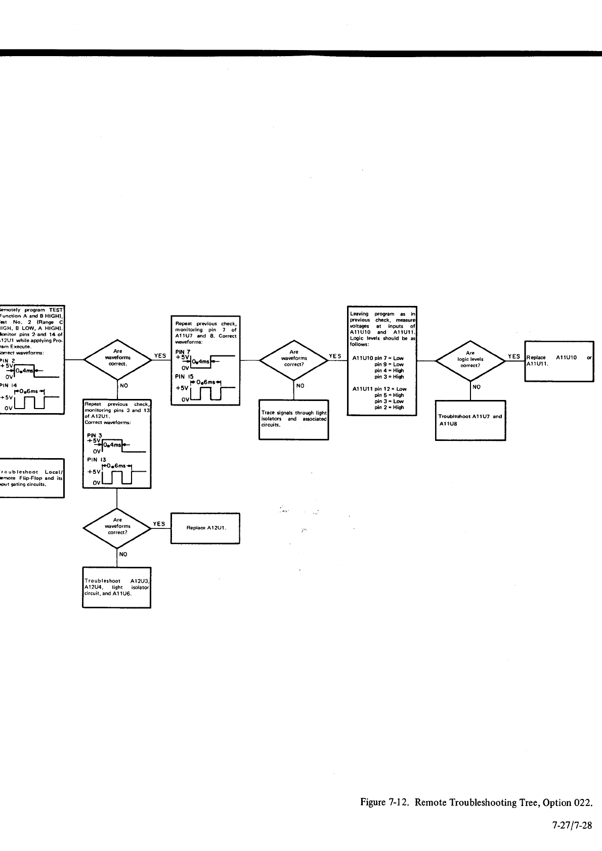
bmtely progmm TEST
Fuodion A and I
6r No. 2 {Range
IIGH.8 LOW,A HIGHI.
lonito. pini 2 and 14 ol
'12U1 while applying
Em Ex@te.
ddEwfoam:
rtN
2
*16t1-
PIN
I4
|.0o6 ms
{'l
-:JL|LT
L6Vrn9 gog€h aS
fevioua ch€ck.
rcltagG et inNts
A'llUlO .nd AllUlt
Logic l4l3 should be
A11Ul0pin7=Ld
ßin 9 = Low
pln 4 - Hlgh
pin 3 = High
411Ul1 pin
12
- bw
ßtn 5 = High
pin3!L@
pin 2 - High
Rep€at prwious ch4k,
monitorlng pin 7 of
Al lUT sd 8. Correcr
PIN 7
+{o.c'"F
OV
l-r
PIN I5
l+ 0o6
ms
I
.::LfLr
+s-Y'ml-
ovl
"'t '&.a.r'1
-ilLJ_LT
Trcubl€ih@t At 1U7 and
A1 IU8
Troubleshoor Al
Figare
7-12.
Remote Troubleshooting
Tree,
Option
022.
7-2717-28
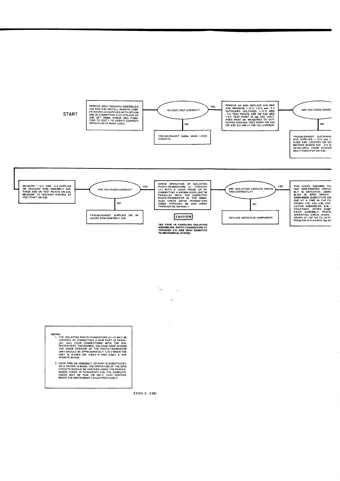
START
BEMOVE
ASCII INGUAFD A$EMALIES
Ag AND 436. INSTALL REMOAE
JUMP,
EF BOAFD
44 ISUPPLIED
WtTB OPTION
OSI IN CONNECIOR
A1J7 IN PLACE
OF
AS. SET 34SA RANGE ANO FUNC-
TION TO TEST i TO VEFIFY COFFECT
OPERATION
OF MAIN LOGIC.
FEMOVE A4 ANO REPLACE Ag AND
436. MESURE + 12 V. + 5 V, ild -2 V
OUTGUAND VOLTAGES. +I2V AND
.2V AEST POINTS ARE ON A32 AND
+5V TEST POINT IS ON A33. VOLT.
AGES MUST BE MESURED TO OUT.
GUAAD GFOUND TEST POINT ON 433
OR A3O. ALLOW +/,1ü TOLLEflANCE.
ARE VOLTAGES
CORRE
TFOUBLESHOOT OUTGUART
AGE SUPLIES. +12V .d +
PLIES ARE LOCAT€D ON OU
MOTHEF EOAFO A3I. .2 V SI
trVELOPED FROM SYSTEM
MULTIVIBAATOF ON
A32,
MENURE + 12V ANO .2V SUPPLiES
q IilGUARO ROM SEMBLY A34.
THESE AR€ ON TEST POINTS ON A34.
MENURE TO INGUAFO GROUNO AT
EST POINT
ON AS,
CHECK OPEAATION OF ISOLATING
PHOTO.TFANSISTOAS U1 THAOUGH
UII WIIH A LOGIC PROAE OR AY
CONNECTING A KNOWN GOOD UNIT IN
PARALLEL WITH THE SUSPECTED
PHOTO.TRANSISTOB IN THE g9OA.
A60 CHECK DFIVE TRANSISTOFS
AM4 THROUGH @ AND A35OI
THBOUGH
04. * Note l.
TROUBLESHOOT SUMLIES
GUARD FOM A$EMBLY AA. FEPUCE DEFECTIVE COMPONENT.
THIS CHECK A$UMES THI
ONE GPIBPRINTED CIFCUT
ALY IS DEFECTIVE. USINC
ELIES IN GPIB REPAIR
OAS8m. SUBSTITUTE A$
ONE AT A TIME IN THE FO
OROEB: A32, AS. A36, A34,
LATION NS€MELIES A3O,
TOGETHER. AFTER SUS'
EACH ASSEMBLY, PERFO
OPEFATING CH€CK GIVEN
GNAPH 5.7 OA '9 IO DETE
PROBLEM lS CLEARED,
Se No
ffi
6E CAFE IN HANOLItrG ISOLATION
NEMBLIES, PHOTO,TRANSISTOAS U
1
DROUGH !II AAE VERY S€NSITIVE
TO MECHAtrICAL STRE$.
ilotEs:
1. THE ISOLATING
PHOTO-TRANSISTOBS
U1_II MAY BE
CHECKED BY CONNECTINC A NEW PABT IN PAFAL.
L€L (ALL FOUR CONNECTIONS)
WITH THE SUS-
PECTEO PAAT. THE NORMAL VOLTAGE OROP ACFO$
THE DIOOE POATION OF THE PHOTO.TßANSISTOF
UNIT SHOULD BE APPAOXIMATELY I-75
V WHEN THE
UNIT IS BIASED ON, ASL4_9 AND A35L1 5 ARE
FERRIT€
8EAN.
2, EACH TIME AN SSEMALY OR PAFT ISSUBSTITUTEO
OR A REPAIF IS
MAOE, THE OPEBATTON
OF
THE
GPIS
CIACUITS
SHOULO 8E CHECKED USING THE PEAFOF-
MANCE CHECK IN PARAGRAPH
545, THE COMPLETE
CHECK MAY BE BUN, OA ONLY THAT PORTION
WHICH THE INSTRUMENT FAILEO PREVIOUSLY.
3490-D
-
3381
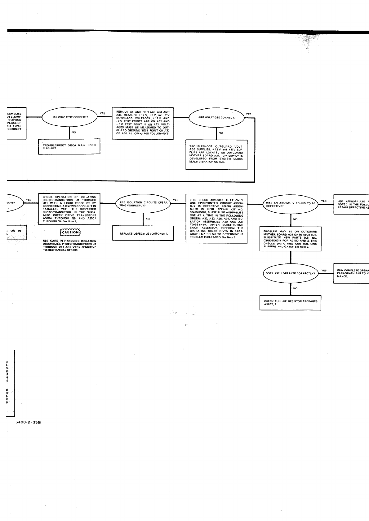
BEMOVE 44 ANO NEPLACE Ag ANO
A36. MEASURE + 12 V. + 5 V. sd .2 V
OUTGUARO VOLTAGES. +12V AND
.2V TEST POINTS
AAE ON A32 AND
+5V TEST POINT IS ON A33. VOLT.
AGES MUST AE MEASURED
TO OUT.
GUABO GAOUND T€ST POINT ON
A33
OF A3O. ALLOW +/.
16 TOLLEAANCE,
IROUELESHOOT OUTGUARD VOLT.
AGE SUPPLIES.
+lzv .nd +5V sUP-
PLI€S ABE LOCATEO ON OUTGUAFD
MOTHEF EOAAO A3I. ,2 V SUPPLY IS
OEVELOPEO FROM SYST€M CIOCK
MULTTVIAAATOF ON A32.
CHECK OPERATION OF ISOLAIING
PHOTO.TRANSISTORS UI THFOUGH
UTI WITH A LOGIC PROBE OF BY
CONNECTItrG A KNdN GOOD UNIT IN
PABALLEL WITH THE SUSPECTED
PHOTO.TNANSISTOR IN THE 3$A.
A5O CHECK ORIVE TRANSISTOFS
A@ AHFOUGH @ ANO A35O1
THBOUGH
04.Se Note l.
ANE ISOLATION CIRCUIE OPERA-
TING
CORFECTLY?
THIS CHECK SUMES THAI ONLY
ONE GPIBPRINTEO CIRCUIT AS€U-
aLY 15 OEFEqIVE.6rNG A$€M.
BLIES IN GPIB REPAIR KIT NO.
OSS.A(rc, SUSSTITUIE A$EMALIES
ON€ AT A TIME IN THE FOLLOWING
OROEF: A32, A3, A36. A34. AND ISO-
LATION SEMBLIES AS ANO A35
TOGETHEA. AFTER SUBSTITUTING
EACH ASSEMBLY, PERFORM THE
OPERATING CHECK GIVEN IN PARA.
GAAPH 5.7 OR '9 TO OETERMTNE IF
PROBLEM
IS
CLEAAED.Se Note 2,
PROELEM MAY AE ON OUTGUAAD
MOTHER BOAFO A3i OR IN A$It AUS.
SUBSTITUTE NEW 'AFE {KIT NO.
ogw@31) FoB a3ru2 aND 3. TH|S
CHECKS OATA ANO CdTNOL LINE
BUFFERS ANO GATES. Se Note 2.
rcES ASCII OPERATE COFRECTLY?
USE APPROPAIATE R
NOTEO IN THE FOLLO
REPAIR
OEFECTiVE
S
Hffi3
6E CAAE II HAXOLING ISOLATION
SEüBIIES. PHOTO.TAAilSISTOAS U1
üBOUGH Ul' ARE VEFY SENTIVE
TOTEqAXICAL STßES.
iE
L.
s-
F
B
IE
o
a
t-
E
N
3490-D
-
338r

r'AT€ REPAIF KIT AS
E FOLLOWING
STEß TO
- VE ASEMELY,
crYYYYrrrFr
l cauil oN.l
ROM AßD MOS DEVICES AR€ EASILY
DESTBOYED BY SIATIC CHARGE.
KEEP PINS SHORTEO WITH CONDUC.
TIVE FOAM OA METAL fOIL WHEN
PART IS NOT IN If,STAUMENT.
Figure
7-13.
GPIB
I/O Troubleshooting
Tree, Option
030.
IF ISOLATION
S€MALY AS ANO
A35
15 DEFECTIVE, GE NEPAIR KIT NO.
OSS@I3 TO NEPAIB 8Y R€PLAC.
ING
DEFECTIVE
COMPONENT{SI.
8UN COMPLETE OPEFATING CHECK IN
PAFAGFAPH 5.45 TO VERIFY PERFOF.
CONNECT LEOP
LINE AT REAR PANEL
@NNECIOR TO GFOUNO U12 PIN 9
TO PIN 24I ANO MONIIOR LFST AT
COLLECTOF OF A3M1. LRST SHOULO
BE LOWWH€N LEOP
IS
LOW.
CHECK INVEATEF AWg PINS
8 ANO
9, AND INGUAFD INVEATER 435U3
PINS A ANO 9.
IF INGUAFO PFOGRAM
ASEMSLY AS
IS OEFECTIVE, USE REPAIR KtT NO.
@96@5 IO FEPAIR AY BEPLAC-
ING
DEFECTIVE COMPONENT{SI.
IFOUALESHOOT RESET CIBCUIT,
AMl 3 AND ASU4 PINS
3
AND 4.
IF OUTGUABO OATA ASEMELY A33 IS
D€FECTIVE, SE REPAIR KIT NO.
OS9OAMS TO AEPAIR AY REPLAC
ING DEFECTIVE COMPONENTIS}.
IF INGUAFD FOM A$EMALY Ag IS
OEFECTIVE, USE AEPAIA KIT NO-
0349O,AOO34 AN D F€PLACE ALL
MICBOCIBCUITS
EXCEPT FOM-
A34U5,
IS PROBLEM CORSECTEO?
IF OUTGUARD ROM A$EMBLY A32 I5
OEFECTIVE. US€ REPAIß KIT NO.
03490.80032 AN D REPLACE ALL
MICROCIRCUIre EXCEPT TWO AOMS
432U2 ANO
3.
RUN COMPLEIE
OPERATING CHECK IN
PARAGRAPH
5{5 TO VERTFY PEFFOF.
MANCE.
FUN COMPL€TE OPEFATING CH€CK IN
PANAGRAPB '45 TO VENIFY PERFdR,,
MANCE.
FEPLACE FOMA32U2.fu NOt€ 2,
REPLACE A32U3. IF THIS CORBECTS
PNOBLEM,
BEPLACE
A32U2 WITH OFI.
GINAL PAßT. IF OPEFATION IS COR-
RECT,
SEE NOTE 2.
7-2917-30
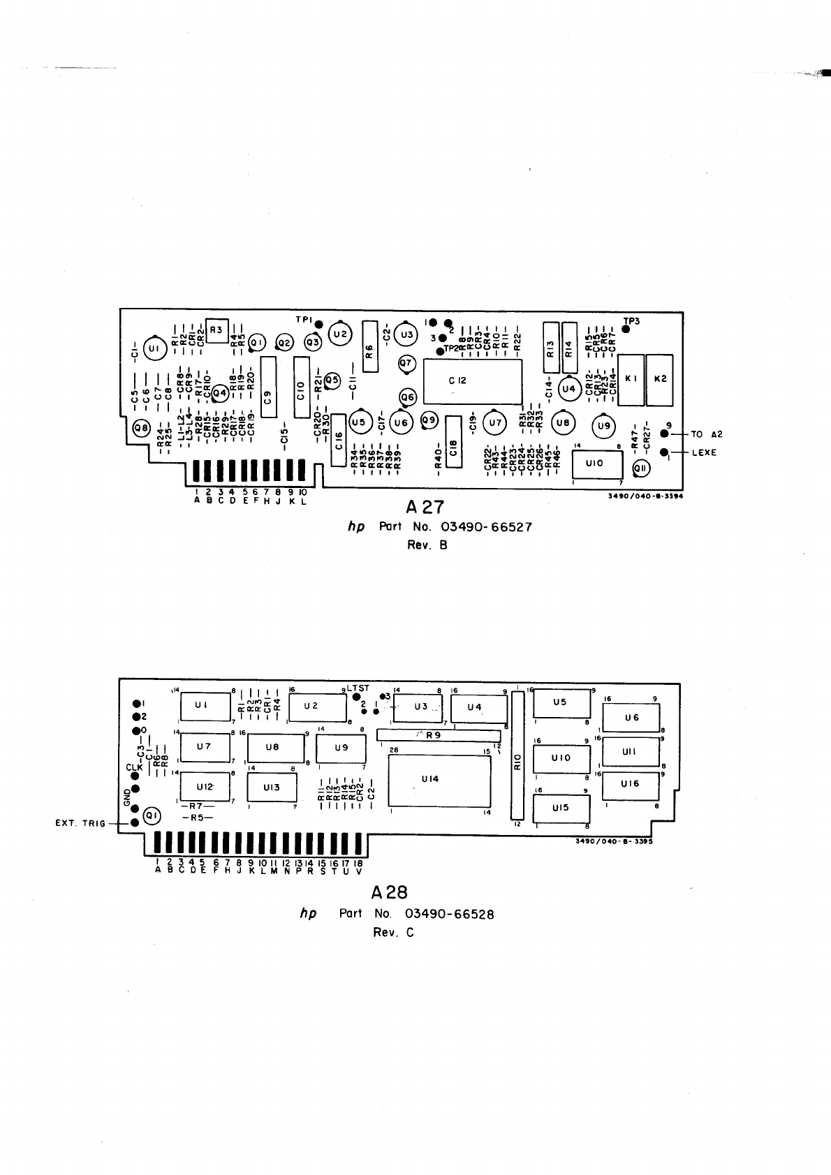
.-.;l
T (6äl
@rö
*üü**ä
TTTTTT
+tr++o
@
ä
+w*+il
[l+
+fr;+tqT
't'*,
llllllllll
hp Porl No. 0349O-
66527
Rev. B
l6|-------19
| ,,c I 16 9
| "" I f-------t
----d ,l ,. l"
16 s 'öl--.le
[ -o ] l u.' I
tl
.r______ä,"1,,"_1"
lllillill
ut4
A28
Port No. 03490-66528
Rev. C
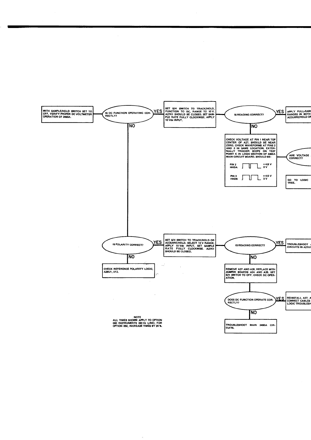
SET SVH SYVITCH TO IRACK/HOLO.
FUNCTION TO OC. RANGE TO lOV,
A27KI SHOULO
8€ CLOSED. SET
SAM.
PLE FATE FULLY CLOCKWISE.
APPLY
10 Vdc
INPt T.
II'ITH SAMPLE/HOLD SWITCH SET TO
OFF, VERIFY PFOPER
OC
VOLTH€TER
OPCRATIOITI
OF 34SOA.
CHECK VOLTAGE AT PIN .I NEAR TOP
CENTER OF A27, SHOULO BE NEAR
ZERO.
CHECK WAVEFORMS AT PINS 2
ANO 3 II{ SAME LOCATIOI{. EXTER.
NALLY TRIGGER SCOPE ON TEST
FOTNT
K IN LOGIC
S€CTION OF 3ISOA
MAIN
CIRCUIT BOARD. SHOULD B€:
PtN
2 +45 V
HHDA I U L-OV
nf-l- üi'"
s€T s/H siltTcH 70 tRAcK/HoLo oR
ACOUIAE/HOLD.
SELECT TO V RANGE.
AP?LY lovdc INFUT. SET SATPLE
RATE FULLY CLOCKYVISE.
AZ'K1
SH(ruLD BE CLOSEO.
REMOVE
A27 AND A28. REPLACE
WIB
I'MP€R EOAROS
A24 ANO A25. SET
S/H SWITCH
TO OFF. CH€CK
DC OPER.
ATION.
YES APPLY FULLf,AI{(
RANGES
IN BOTH
ACOUIRE/HOLD
OP
AnE VOLTAGE /
CORRECN
TROUALESHOOT
/
ctRcutß tN A2tut
NOTE
ALL IIMES SHOITT{ APPLY
TO OPTION
0d) INSTRUMENTS
(6OHz LlilE). FOR
OPTION O5O, INCREASE
TIMES
BY 20 i.
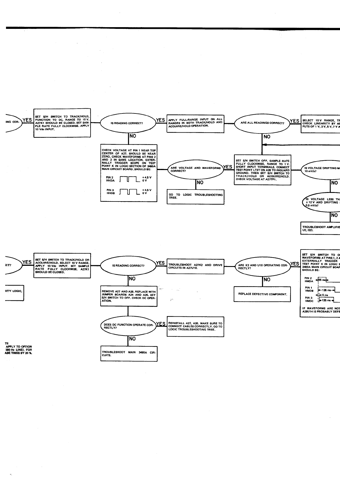
It{G @R-
SET S/H SAYITCH TO TFACK/HOLD,
FUNCTION TO DC, RAilGE ?O lOV.
A2'K1 SHOTJLO 8E CLOSEO.
SET SAM-
PLE RATE FULLY CLOCKS'ISE.
APPLY
10 v& tNruT-
MLY FULLAANGE INR T Ot'l ALL
RANGES
IN SOTH TRACK/HOLD ANO
ACOUIRE/HOLO
OPERATION'
CHECK
VOLTAGE AT PIN ' NEAN
TOP
CENTER OF A2'. SHOULO SE NEAR
ZERO.
CH€CK WAVEFORiilI AT PINS
2
AND 3 IN SATE U)CA?ION. EXTER.
NALLY TRIGGEB SCOF€ Oil T€ST
?otNT x tN Loctc sEcTtoN oF 3!90A
MAIN CIRC-I'IT
8OAFO.
SHOULO AE:
PtN
2 +45 V
HHoA .l U Lov
PtN
3 +45 V
HHoE J ll L_ 0V
SET S/H S:II,ITCH
OFF, SAMPLE
RA?E
FULLY CLOCKWISE,
RANGE IO 1 V.
SHORT II{PUT TERMINAI.s. Cor{ilECT
TEST POINT
LTST ON
A28 TO INGUARD
GROUND. THEN SET 6VH
S1INTCH TO
TRACK/HOLD OR ACOUIRE/HOI'.
ffECK VOLTAGE
AT A27TPI.
YES SELECT IOV RANGE. TF
CHECK IINEARIW 8Y A'
PUTS
OF r V.3V,6 V,7 V A
IS
VOLTAGE
OßIFTING
T(
lOmV/.?
VOLTAGE LESS TH/
i 12 V ANO DRIFTII{G
I
TROUBLESHOOT
AIPUFI€
rn,@t.
SET S/H SiWIYCH TO ol
tvavEFonMs aTP|l{s t,2 l
EXTERNALLY TRIGGER
TEST POINT K IN LOGIC
S
3,l9OA
MAIN CIRCUIT
BOAR
SHOULO
gE:
.F;t
F;;L
Jha^
F*;l__
PIN 2
HMOA
PIN I
HMDS
PIN 3
HMOC
IF WAVEFORMS
ARE NOT
A28UT4
IS
PROSASLY
DEFE
'E
AFPLY TO OPNOß
(@Hz UN€l. FOR
ASE nilES BY m *"
SET S/H SIVITCH TO TRACK.IHOLO OR
ACOUIRE/HOLD. S€L€CT l0 V RAtrlGE.
APPLY tovdc lNPUt. S€T SAPLE
RATE FULLY CLOCKITIS€. A27KI
sltoulD 8€ cLosEo.
TROUEL€sHOOT A27X2 ANO ORIVE
ctRcutTs tN A27Ut0.
REMOVE
A27 ANO
A2A. REPLACE
IVIIH
JUMP€R AOARDS A24 AND A25. SET
S/H SI\'ITCH
TO OFF.
CHECK OC
OPER-
ATION.
T A27, A?a. MAKC SURE
TO
CABLES
CORRECTLY.
GO
TO
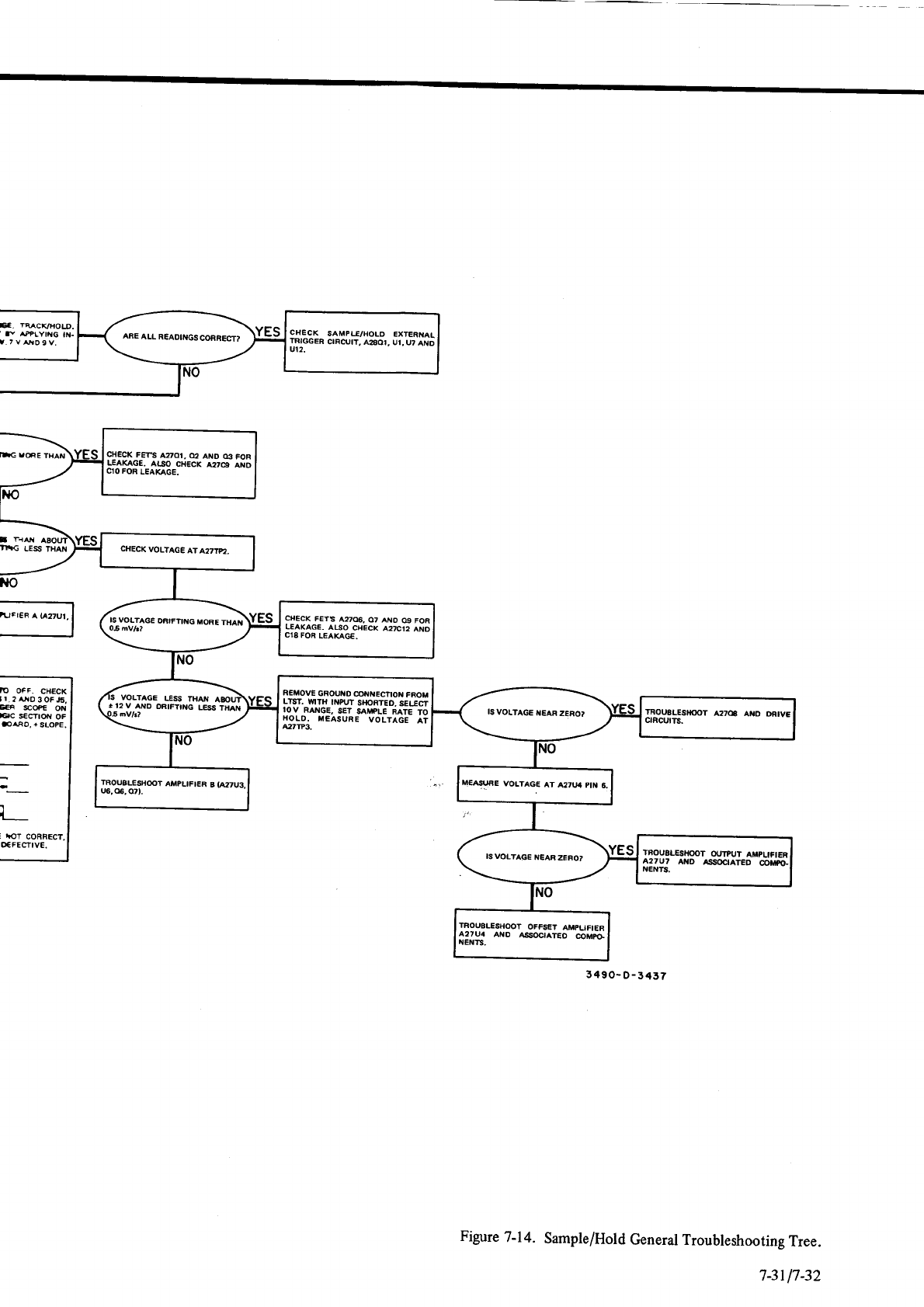
M YGE THAN
I Iiü
'NG LESS THAN
NO
. oft-".*l
tr 2uo30FJ5, l
EB SCe€ ON I
EC S€frtOil OF I
f mO, +
SLOPE.
I
I
I
r_l
L_l
: rrOT CORRECT,
I
o€FEnrvE. I
Figure
7-14. Sample/Hold
General Troubleshooting
Tree.
CHECK
FErS azot, 02 Aito o:t FoR
LEAKAGE. ATSO CHECK A27C9 ANO
CIO FOR
LEAKAGE.
CHECK
VOLTAGE
AT A27TP2,
CHECK
FETS A2706, 07 ANO 09 FOR
LEAKAGE.
ALSO
CHECK
A27CI2
AND
C18
FOR
LEASG€.
REMOVE
GROU]ID
OONIITECTIOI{
FROM
LTST. WITH INPUT SHORTEO. SELCCT
IO V RMGE, SET SAi'PLE RATE TO
HOLD. M€ASURE VOLTAGE AT
N7P3.
I 12 V ANO ORIFTING L€SS THAN IS
VOLTAG€
T{EAR
ZERO?
TROUALESHOOT
AMPLIFI€R B
u6, 06, o?t.
ISVOLTAGE
TIEAR
ZERO?
TROUELESHOOT
OFFS€T AMPLIFIER
i:l*o ^no AssocrarEo @MPG
5490-
D-
3437
't3t17-32
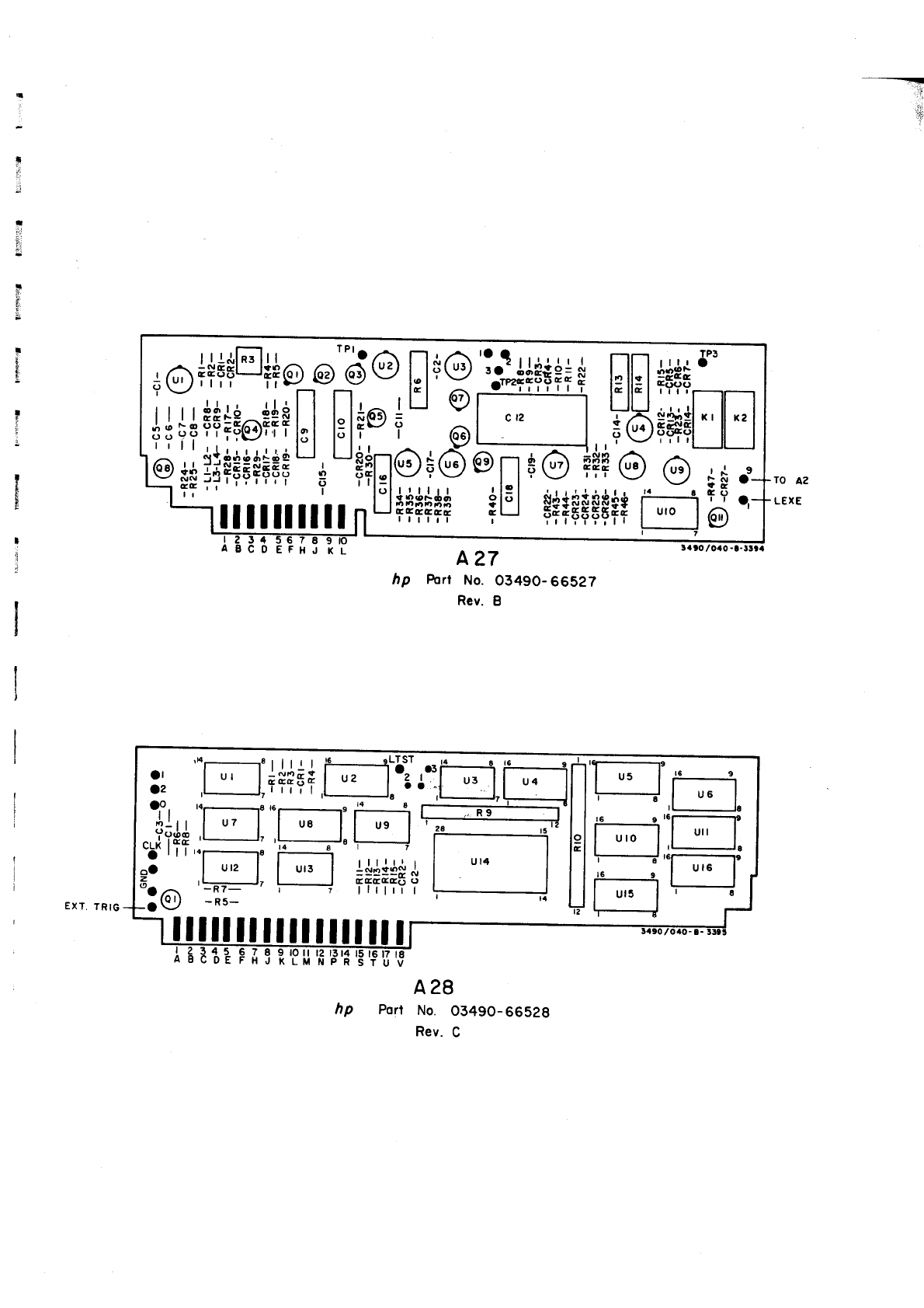
--
ti.
TO A2
LEXE
hp Fort No.
03490-66527
Rev.
B
A28
Port No. O349O-66528
Rev.
C
ut4
l€f---19
l"lH
i---i,l ,. L
t6 9,öl--19
[l-] 1,,' I
| | rr re
]-ä lsr-le
t6 e I ul6 |
tt
Itlllllilt iltf il I
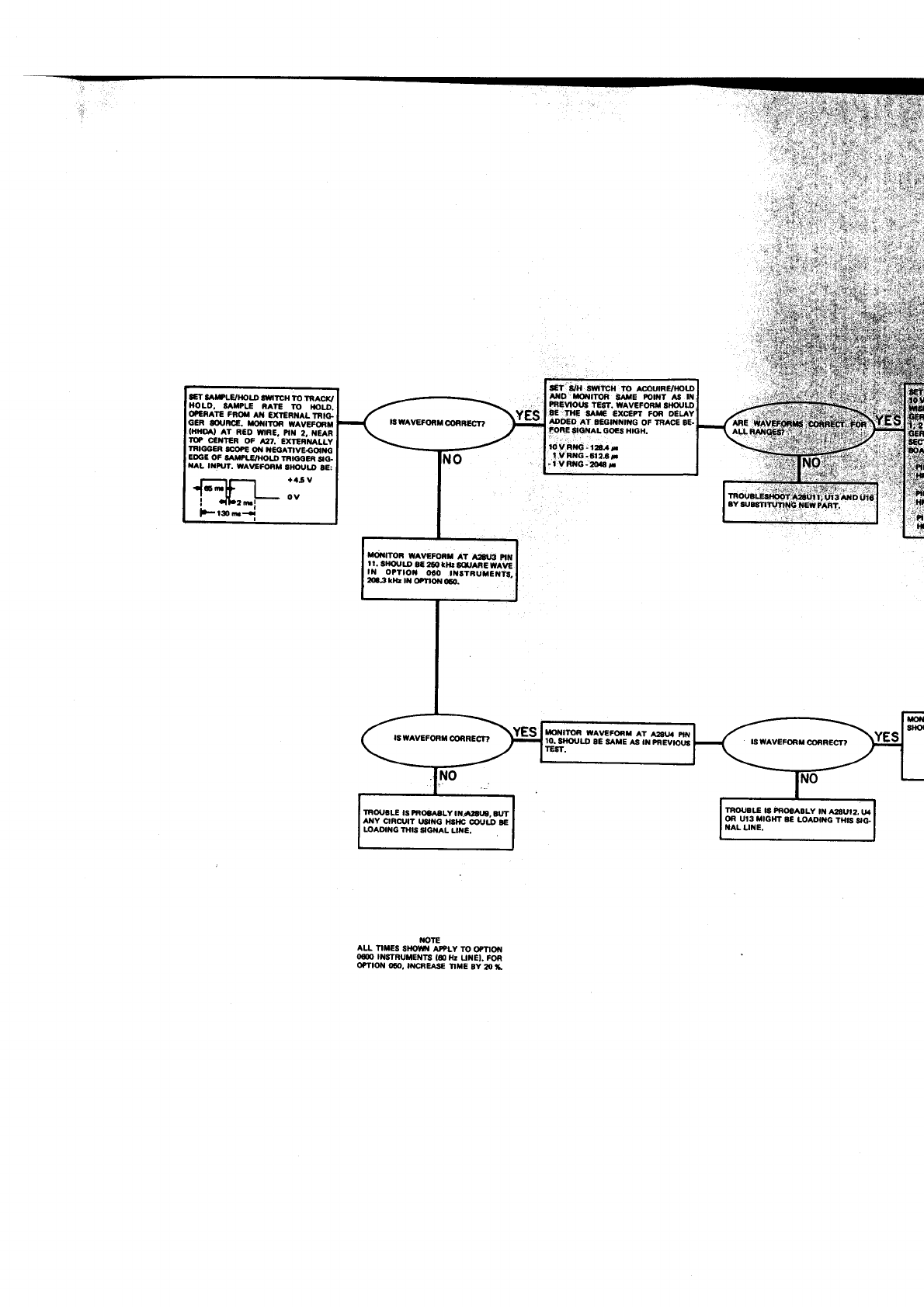
sET s/H slriilH to acoutRE/lrolD
Ar{D toa{ron a IE PotftT a5
aE rH€ iar|E €xcE7t Fon oELAy
ADDEO AT BEGIIIilI]IG OF TRAC€ IE.
IORE SIGI{AL G()€S HIGH.
:l
lO V Rilc - t28a r
t.v Rilc -El2,6f
-l VRlfG-2oaaF
8Ap|-crt{ot aw|rcH To rR^cx/
HOLO, TAXPLE RATE TO IOI.D.
O?€FATE FhOX A1{ EXIERI{AL TRIG.
gtt FcE. t|(tt|Toa wAv€Foau
IHHOA' AT RED ffRE, ?II{ 2, '{EAR
IOP C€I{TER OF A27, EXTEFNATLY
TRIGGCR 8CO?€ Oil TEOATIVEGdMT
EOGE
OF .AIPLI'HOU) TRIGGCR
!G.
tilru?. xrav.EFoau
810uu) aE:
TOilITOR WAVEFORI AT AztIJi' NiI
I l. SlrOUr-O 0€ 26at kH: glr^hE yyAVE
r1{ oPttolt t
60 tI8TRUCCt{ß-
263 klL tll (t?tot{ co
lrot{tToi TYAVEFORI At A28Ura Pill
lojltot u) 8c sA[E AS |N PnEvlous
TROUELE IS 'ROSAALY IT{Ä'8I,9, 8UT
aNY c|RCt IT USll{G H8t{C @UU' rE
IOADIilG THIS SIGilAL UNE.
TRq'8LE |8 PNOEAELY
IT A28UI2,
I,l.
on ut3 iltcHT 8E
tOAOtilc
THIS
9c.
NAL LIl{E.
;,t:r.1i
'i+
:l:?ll
'lf
TOTE
ALL flrES SI|oü,'{ Ar?lY TO O?TtOl{
OdD INEIRUilEIITS Iü) Ht UXEI. FOfi
oPTtoit 60, ncnEAsE nil€ 8Y 20t
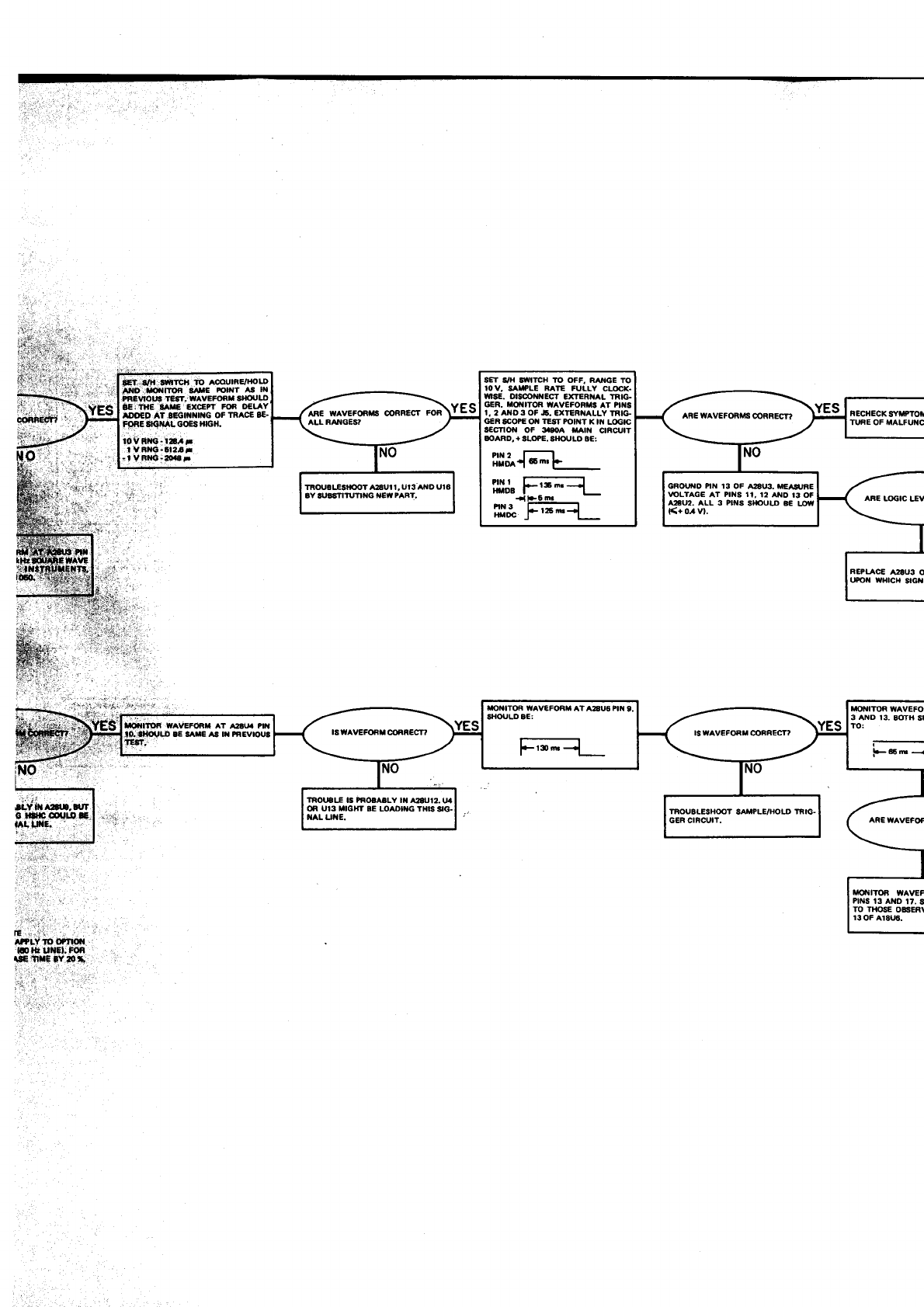
SgT S'H I|S'ITICH TO OFF, RAI{GE TO
IO V. SAIT?LE RATE FULLY CL@X.
TVI8E. OISOONI{ECT EX'ERilAL TRIG.
GER. I{OI{ITOR ü'AVEFONil3 AT NilS
I, 2 AiIO 3 OF J5. €XIERNALLV TFIG
GER SCOP€ Oil TEST FOINI K It{ LOGIC
S€CTION OF 3'l9OA llAll{ CnCUIT
EOARD, + SLO'E. S}|o{,LO AE:
l,ffi.f-L_
'JüJ,
F _
4FEm
#s F,;E_
üET .srH tuttrcH io AcoulRE/HoLD
ailo xoilrToa 8Af,E FolilT As lN
?REVIOI,'3 T€8T.
WAVEFORT A}('(,LO
.!E:?HE tAIE'EXCEP? FOR
D€LAY
Itro€D At.gEGr{für{G oF TRACE
gE-
FgiEsrg{ LGOCSHIGH.
rävnG.ii;r
I YFIG-6!2.0r
,t vFl{G:20a8f
TRouaLEsltoor A28ufi
.
ur3AilD ut6
6Y SUISTITUTING
'{EIV
PART. GROI'TO PIN 13 OF A28U3. TEASJRE
VOLTAG€ AT PINS 1I, 12 ANO 13 OF
A28U2. ALL 3 P|NS SI|OULO g€ LO|Y
t<+ 0, v),
FECHECK
SYTPTOT
nnE OF l,lALFUl{C
ARE LOGIC IEV
REPLAC€ A26U3 O
uFo?t wt{lct{ stcia,
TONITOfi ITAVEFORI' AT A28U8 PIiI 9.
SHOULO B€:
Fr3fra_
t(iüToH MVEFORI| AT A2Arr4 Ail
to;tllolraD rE sArE as n tnEvDrrt
t!-3I;
TFOi Bt.E ls PROEAaLY lt{ A28Ut2. t il
OR UI3 |,IGXT BE LOAO|I'G THIS
3G.
l|AL Ut{€.
uot{tToR yYAvEFol
3 AND t3- AOTH Sr
TO:
i.-
P65ü<
AR€ WAVEFOq
uoillToR wAvEF
P|NS
t3 A1{O
17, E
TO THOSE O88ER!
130F Ar8U6.
^FLV ro iztnifl.
aolts ur{Et;
Foa
fi*''r*
:,,;'):11'.:
" ' '
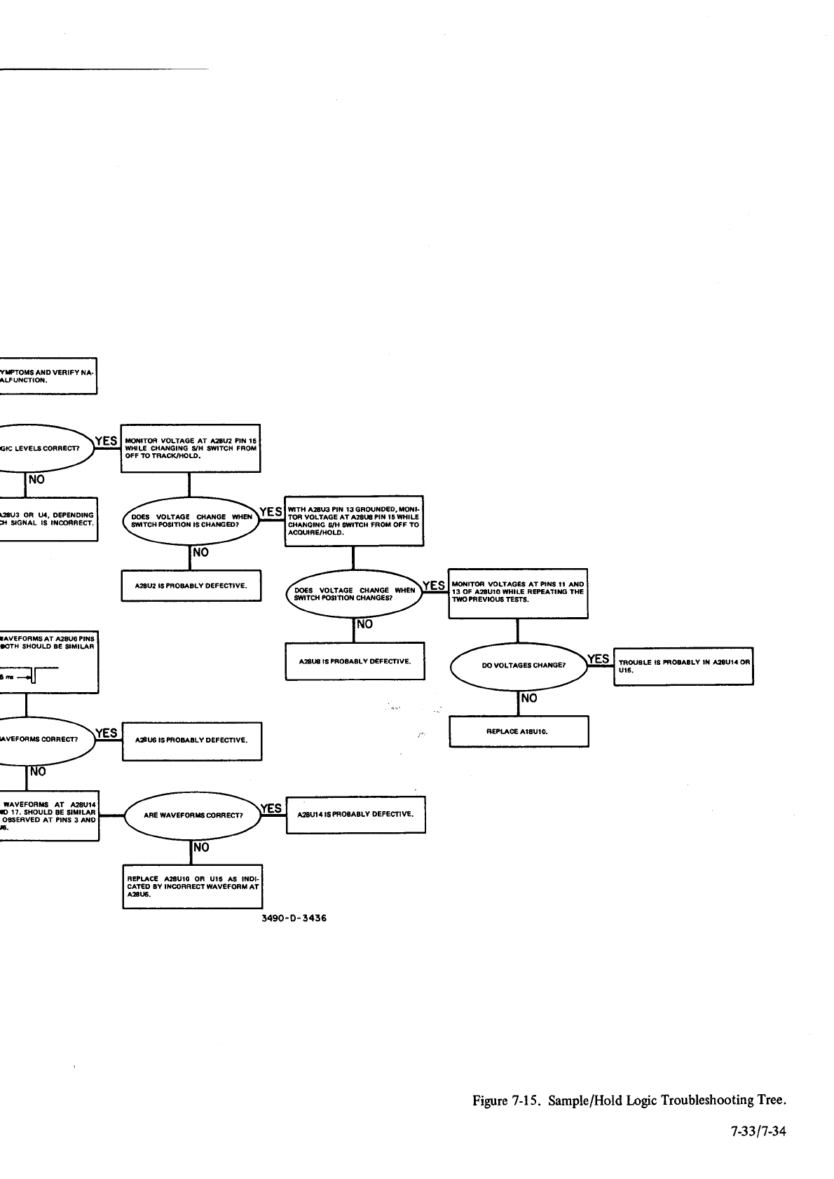
YTFTOTIS
AilD VERIFY NA.
ALFUNCTION.
\24U3 OR tjl|, OEPENDII{G
>r srcral ts r{@RREcT.
IAVEFORMS
AT A28U6
PIilS
FTH SHOULO
BE
SIMILAR
MONITOR VOLTAGE AT A2ATN PIN 15
U'HIL€ CI{ANGING S/H STIITCH FROil
OFF TO TRACK/HOLD.
A28U:l
PtN r3 GFOUT{D€D.
mot{t-
TOR VOLTAGE AT A2ATß
PIiI 16 WHILE
S/H SIYITCH FROT OFF TO
OO€S VOLTAGE CHATGE WHEX
S{UITCH
FOSITIOT
IS CHAiIGED?
iTOI{ITOR VOLTAGCS AT PINS II AND
I3 OF A28UTO WHILE REPEAT|TG IHE
TUTO PREVIOTJS
TESTS.
A28U2 IS PROBABLY DEFECTIVE. DO€s VOLTAGE CHANG€ WHEf{
SIVITCH
POSITION
CHANGES?
a28t 8 ls PnoEaaLY o€FEcTtvE.
;AVEFORMS AT A28UI4
F I7. SHOULD
BE SIiIILAR
o€s€RvEo AT P|NS
3 AltO
Ä
Figure 7-15. Sample/Hold Logic
Troubleshooting
Tree.
REPLACE A28UIO OR UI6 AS INDI.
CAT€D BY IN@RRECT YYAV€FORI'
AI
A'BIJ6.
3490-
0- 3456
73317-34
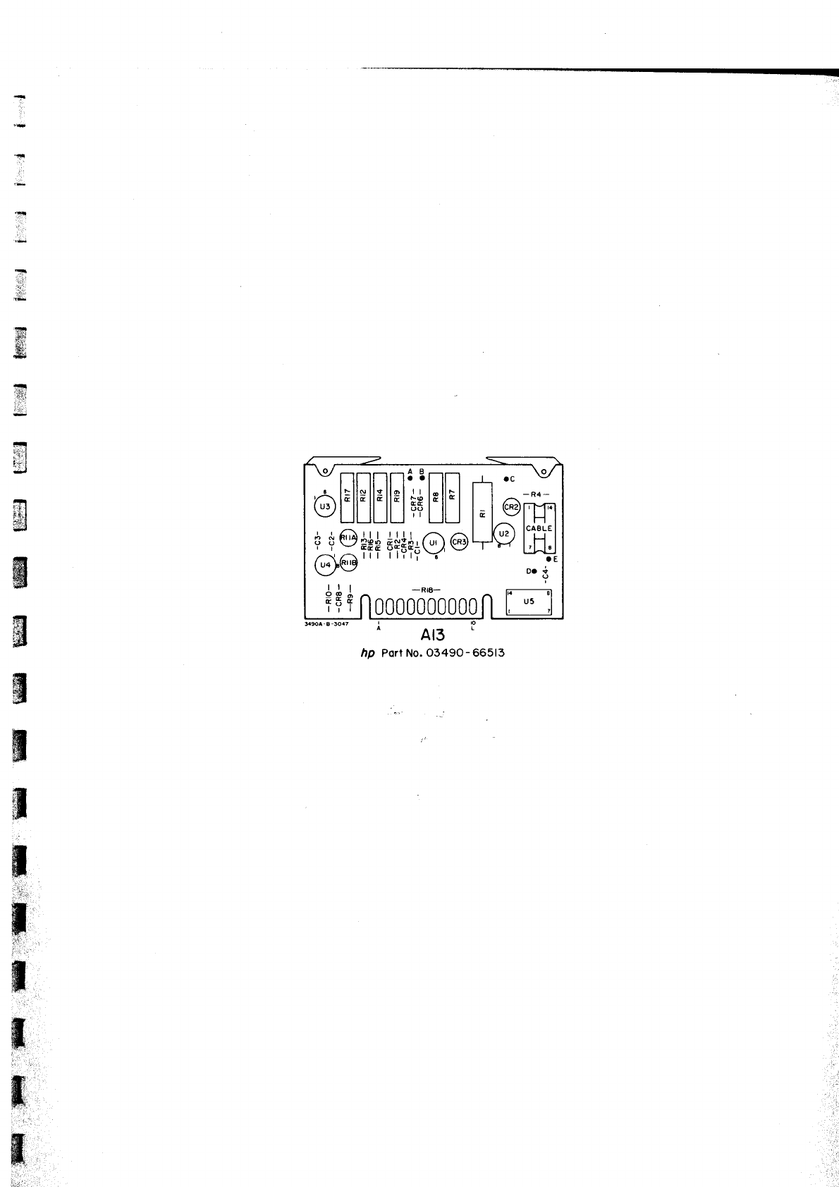
hp Pott No.
O349O- 66513
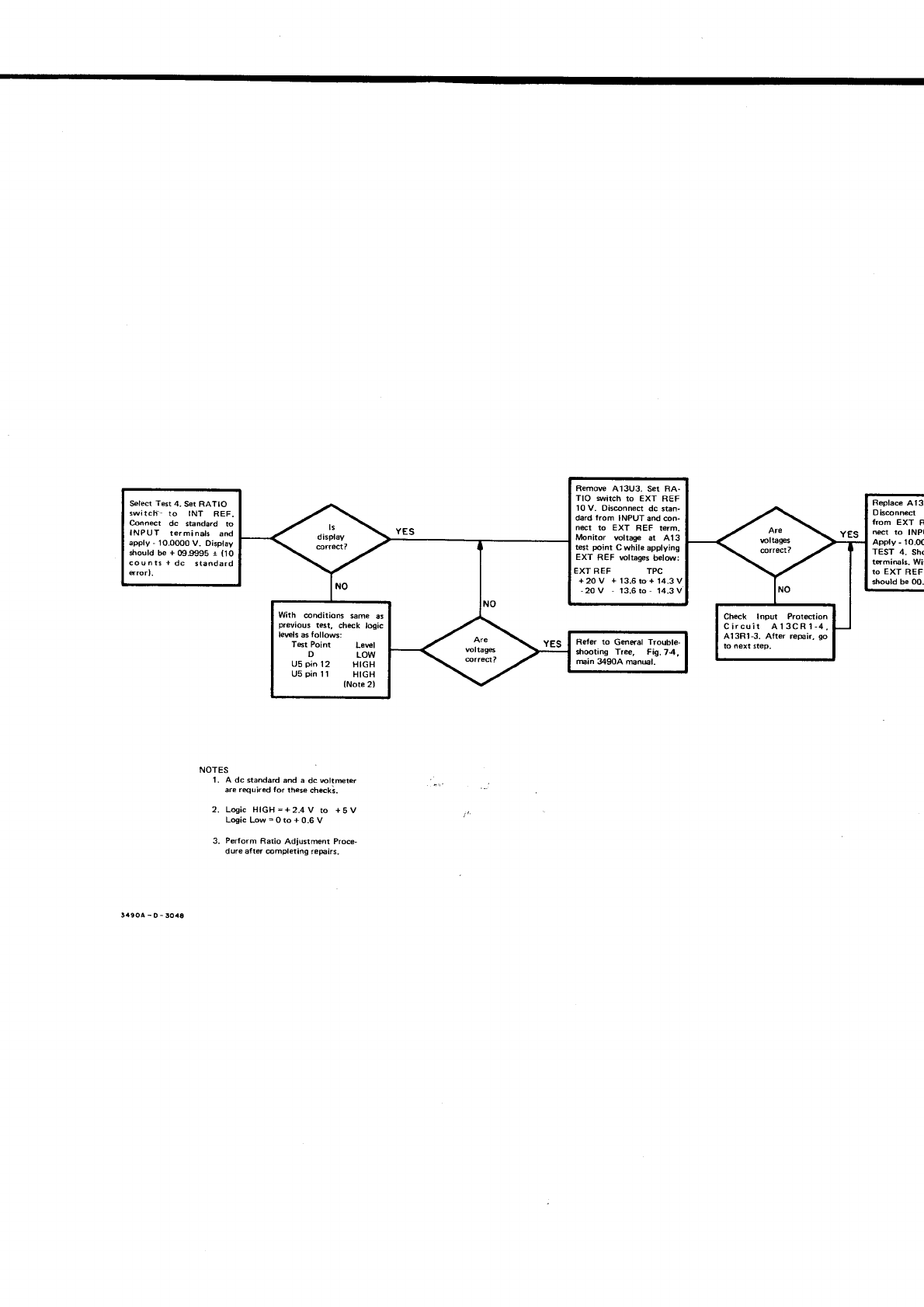
Remow A13U3, Set RA-
TIO $itch to EXT REF
10 V. Ois@nnect dc stan-
dard from INPUT and con-
net to EXT REF lerm-
Monitor wltag€ at A13
test poinr C whil€ applying
EXT REF wltages below:
EXT REF TPC
+20V +13.6ro+14.3V
,20V - 13.6to- t4.3V
Select Test 4. Set RATIO
switch-- to INT REF.
Conn4t dc shndard to
INPUT terminali and
apply
- 10.0000
V. Display
sbould b€ + (x).9995 I {'lO
counts + dc atandard
qrorl.
With @nditions sme as
previous test, ch4k logic
lewls 6 follows:
T6t Point Lowl
D LOW
U5
pin 12 HlcH
U5
pin
11 HtcH
lNote 2l
Ch*k Input Prot@tion
Circuit A13cRt-4,
A13Fl1-3. Afrer rep6ir,
go
to next step.
Refer to Gdffal Trouble-
*r@ling Tree, Fig.7.4,
min 34904 man@1.
Replace
A13l
Dis@nned
from EXT R
net ro lNPt
Apply - 10.00
TEST 4. Shc
tqmimls. Wil
rO EXT REF
should be 0O.r
NOTES
l. A dc standard and a dc wltreter
are required for these check;.
2. Logic HIGH=+2.4V ro 15V
Logic Low = 0 to + 0.6 V
3. Perform Ratio Adiustment Proce-
dure after @mpleting repairs.
54904-D-loaa
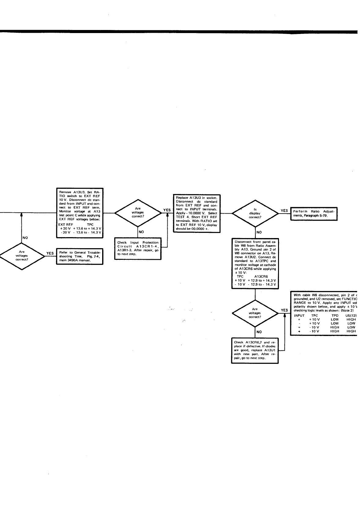
Remov€ 413U3. Set FIA-
TIO sitch to EXT REF
l0V. Disconnect dc atan-
dard from INPUT and @6-
net to EXT REF t6m.
Monitor voltage 4 Al3
t6t point C whils applying
EXT REF bltäges below:
EXT REF TPC
+ 20 V + '13.6
to + 14.3 V
-20 V - 13.6 to
- 14.3 V
Replace A13U3 in $cker,
Disconned dc sbndard
from EXT REF and con-
nEt to INPUT terminals.
Apply - 10.0000 V. Select
TEST 4. Short EXT REF
tfrmiEls. With RATIO set
to EXT REF 10 V, display
should be 00.0000 t.
Perform Ratio Adjust-
ren$, Parag.aph
5-79.
Chrck Inpur Prottrtion
Circuit Al3CRl-4,
A13Fl1-3. Aft* rep6ir,
go
to nexl step.
Disonnect front penel 6-
ble W8 fJom Ratio Asem-
bly 413. Ground pin 2 of
l E @nnector on A'13. Re-
mve 413U2. Connect dc
sbndard to A13TPC and
monitor voltage at @thode
ol Al3CR6 while applying
|to v:
TPC A13CR6
+10V +l2.9to+14.3V
- 10 V - 12.9
to - '14.3
V
Refer to G6eäl Trouble-
s*rooting
Tree, Fig.7.4,
min 34904 man@l-
Check A13CR6,7 and re-
place if deffttiw- lf diodes
a.e good, replace Al3U1
with new Frt. After re-
parr, go to next step.
YES
Wirh €ble W8 dis@nnected, pin 2 of c
grourded, and U2 removed, set FUNCTIO
FANGE to 1o V. Apply any INPUT vol
polaritv lhown b€low, and apply t 10!
c'hecking logic lewls as sh@n: (Note
2,
INPUT
+
+
TPC
f t0 v
+
10 v
-
10
v
-10v
u5{121
HIGH
LOW
LOW
HIGH
TPD
LOW
LOW
HIGH
HIGH
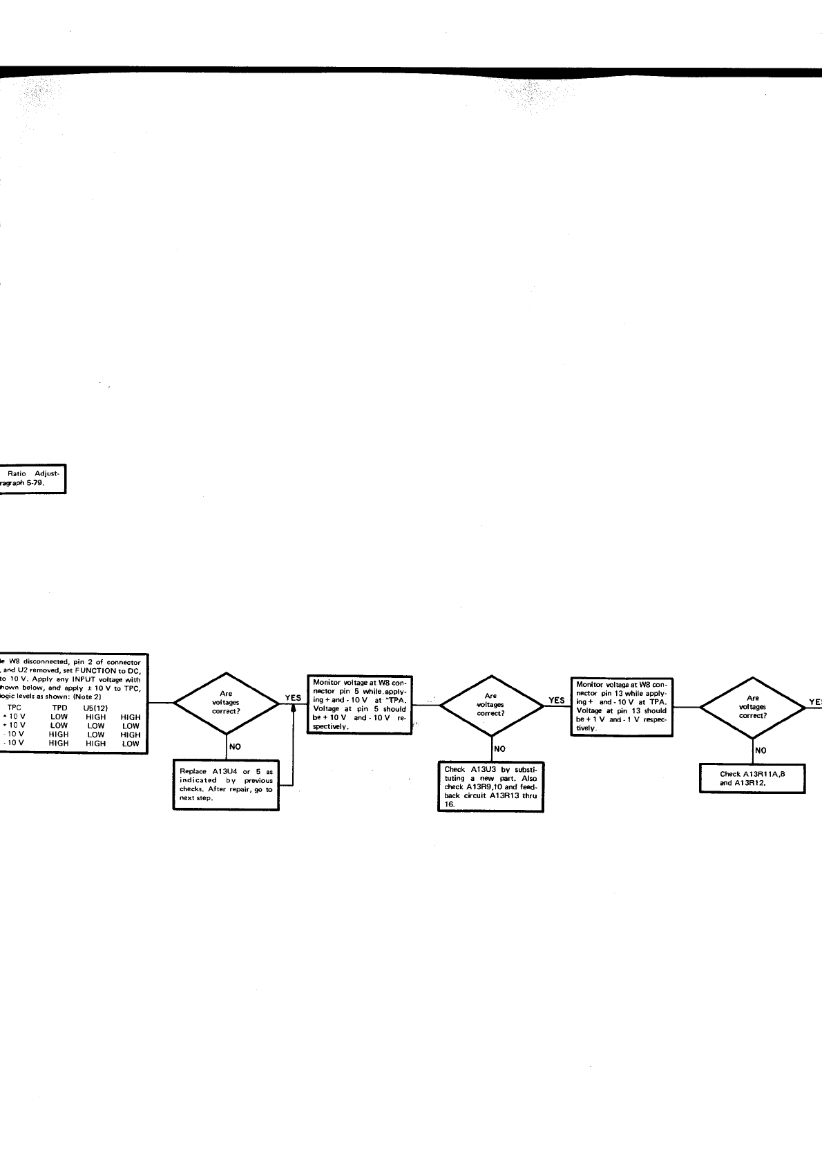
Ralio Adjust-
r4rap6 5-79.
lc W8 disconnected, pin 2 oi connetor
,
ard U2
removed.
set FUNCTION ro DC,
to 10 V. Apply any INPUT voltag€ with
h*n below, and apply I l0 V to TPC.
bgac levels
a! sh@n: lNote 2l
TPC
.
10 v
+
l0 v
10 v
-10v
TPD U5(12)
LOW HIGH HIGH
LOW LOW LOW
HIGH LOW HIGH
HIGH HIGH LOW
Monitor rcltage at W8 con-
n*tor pin 5 while-spply-
ing+and-loV at'TPA.
Voltage at pin 5 should
be+l0V and-10V re-
spectiwly,
nedq pin 13 while apply-
ing + ahd - 10 v .l TPA.
Volhge il pin 13 should
be+1V and-1V r6p4-
tiwlv.
Replace A13u4 or 5 as
indicated by prwious
checka. Atter reFir, go to
next step.
Check 413U3 by subsri-
tuting a ntu p6n. Ale
cl€ck A13R9,tO arld feed-
back cirdit A13R13 thru
16.
Check Al3Bl 1A,8
dd Al3R12,
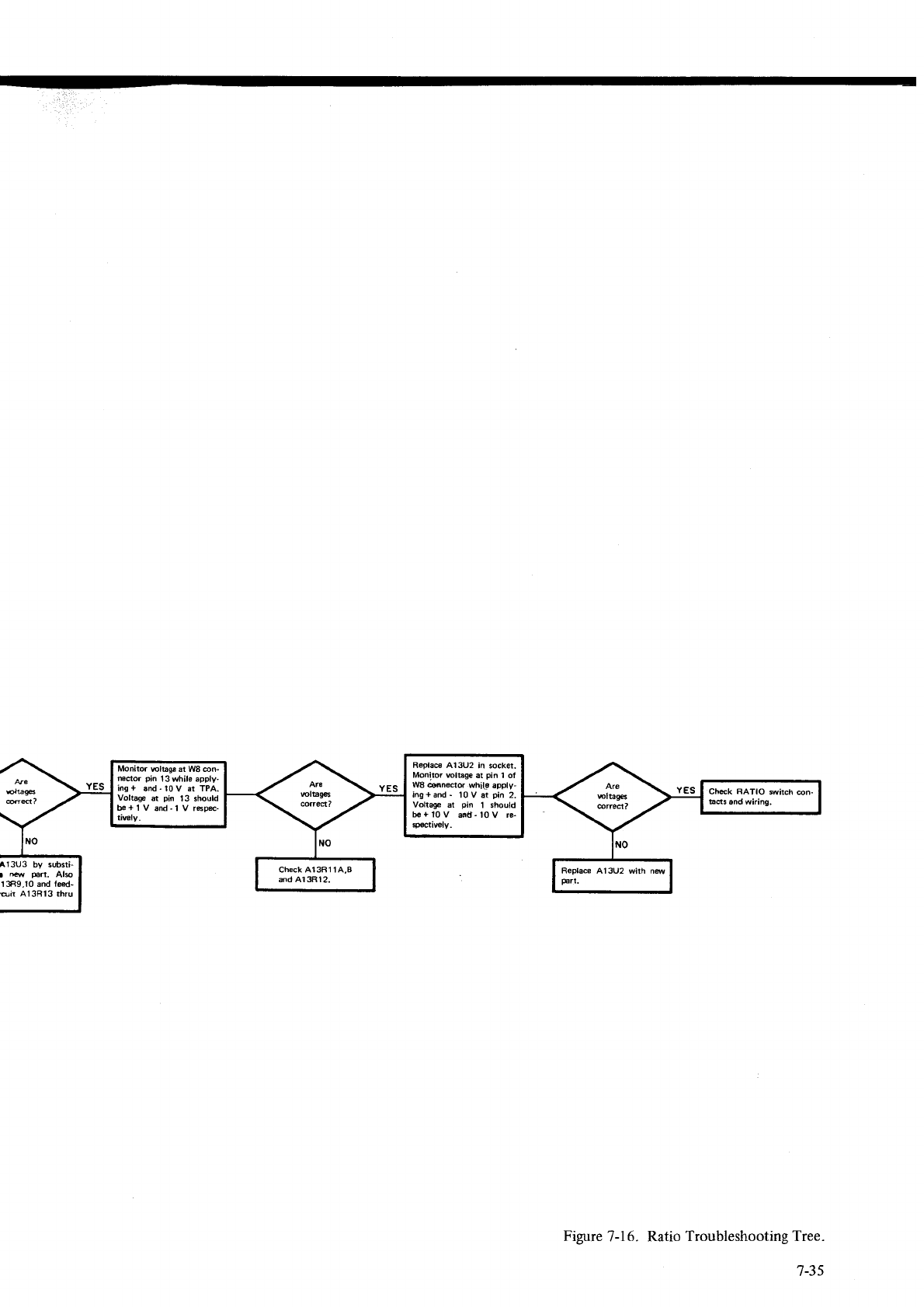
Replac€ Al3U2 in socker.
Monitor wltage at pin 1 of
W8 @nectff whi[6 apply-
ing+and- 10V at pin 2.
Voltage at pin 1 should
b€
+ 10 V arü- l0 V re-
spoctiwly-
Monitor rclbga at W8 @n-
nedor pin 13 while apply-
ing + .nd - 10 V at TPA.
Voltage d pin 13 .hould
be+1V and-l V r6pc-
tiwly.
Chsk BATIO ilitch @n-
laqts and wiring,
A13U3 by substi-
r 'e pan. Als
1 389,10 ard feed-
oh A'l3B13 thru
Figure
7-16. Ratio
Troubleshooting Tree.
't-35
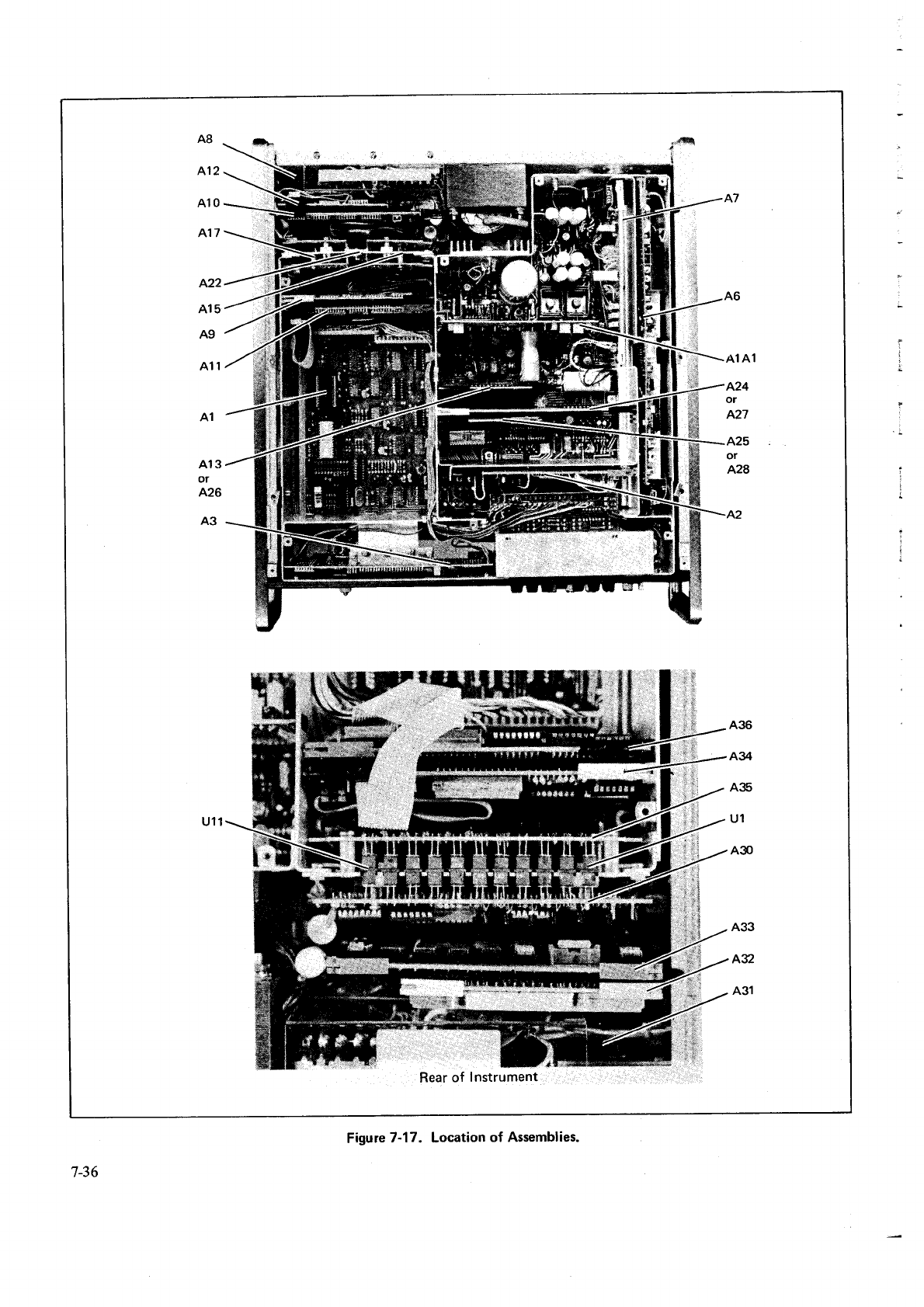
A8
A12
A10
A17
A22
A15
A9
A1
1
A13
or
426
A3
A36
A34
A35
U1
A30
A33
AS2
A31
Rear
of Instrument
7-36
Figure
7-17. Location
of Assemblies.
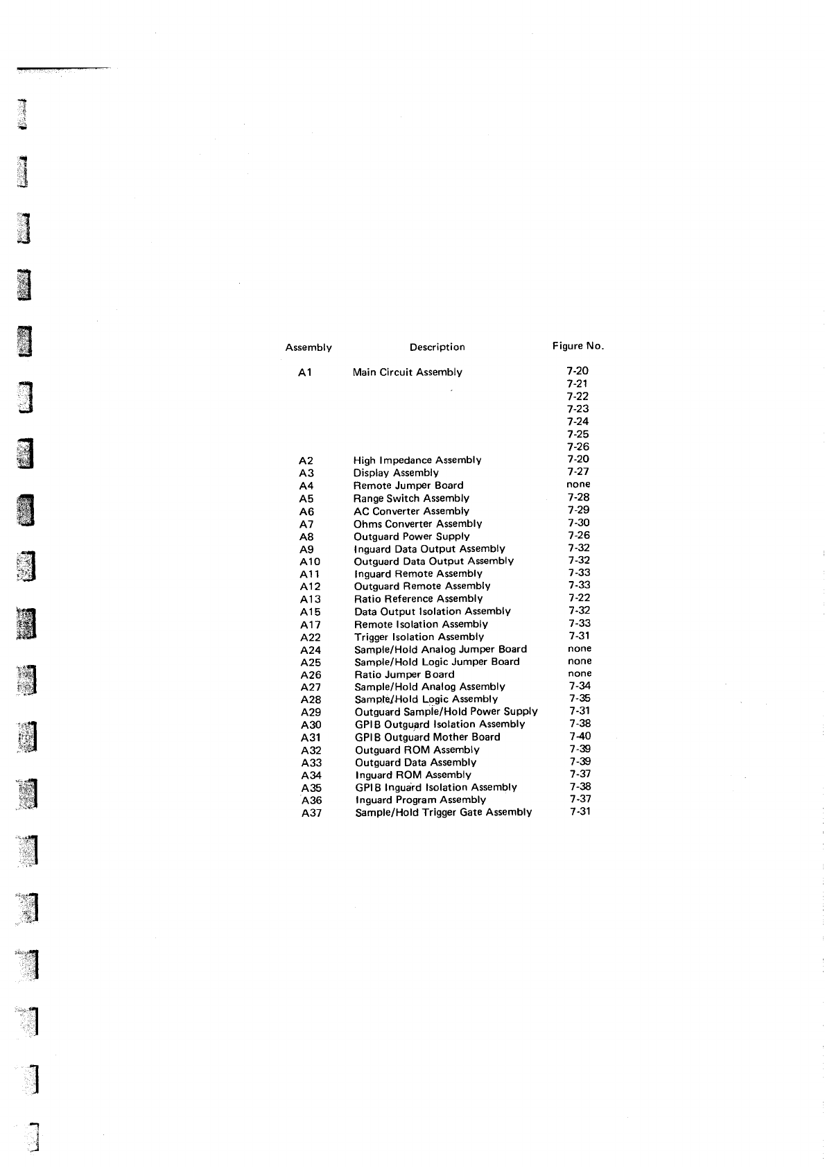
:?
r€
d
ral
r:ä
#
.:..4
']ri*
i3
ä
#l
1:.i11
.111
nt
J
}3
Assembly Description
A1 Main Circuit Assembly
High lmpedance
Assembly
Display Assembly
Remote Jumper Board
Range Switch Assembly
AC Converter Assembly
Ohms Converter Assembly
Outguard
Power
Supply
Inguard Data Output Assembly
Outguard Data Output AssemblY
Inguard Remote Assembly
outguard Remote Assembly
Ratio Ref
erence Assembly
Data Output lsolation Assemblv
Remote I solation Assembly
Trigger lsolation Assembly
Sample/Hold
Analog
Jumper Board
Sample/Hold Logic JumPer Board
Ratio
Jumper Board
Sample/Hold
Analog Assembly
Sample/Hold Logic Assembly
Outguard Sample/Hold
Power
Supply
GPIB Outguard
lsolation AssemblY
GPlE Outguard
Mother Board
Outguard ROM AssemblY
Outguard Data Assembly
Inguard
ROM Assembly
GPIB Inguard
lsolation Assembly
Inguard Program
Assembly
Sample/Hold Trigger Gate Assembly
A2
A3
A4
A5
A6
A7
A8
A9
A10
All
A12
A13
415
A17
A22
A24
425
A26
427
428
A29
A30
A31
A32
A33
A34
A35
A36
A37
Figure No.
7-20
7 -21
7-22
7-23
7-24
7-25
7-26
7-20
7-27
none
7-28
7-29
7-30
7-26
7-32
7-32
7 -33
7-33
7-22
7-32
7-33
7 -31
none
none
none
7-g
7-35
7-3'1
7-38
740
7-39
7-39
7-31
7-38
7-37
7 -31
Fg
rä
':€
1l
1
.-]
,J
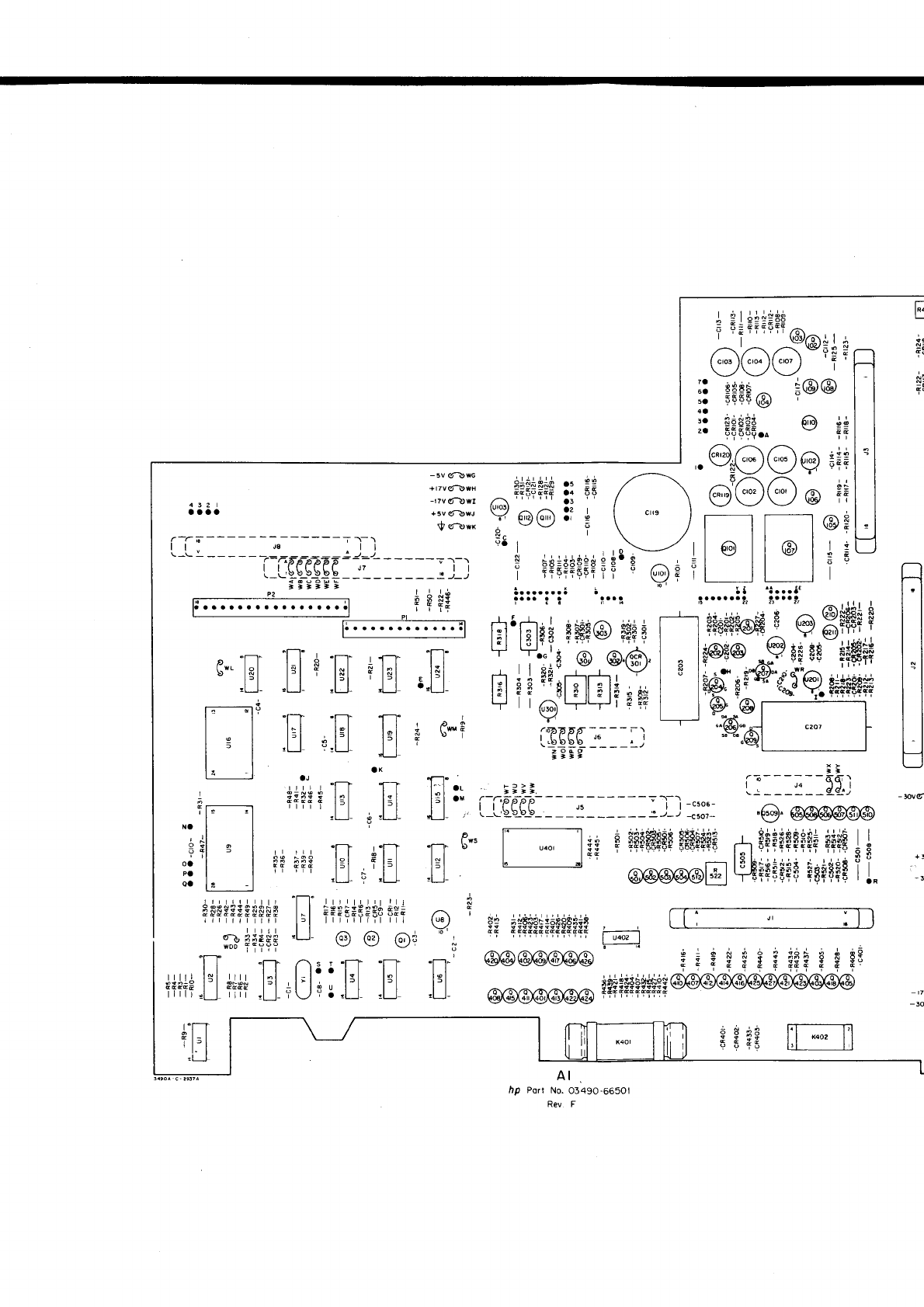
,l,l;
I i; E r-----\
'E
'
| |
I r-:l
/?\ll
\oell
tl
J;l I
f T I I
,,t-l
eTTl
I
;rl I
fTl
I
,tt
rÄ3t I
\gvat:l
' t_l
I
+l
I
;
=u
T' n
l=l
U
n
l,l
L--1
| ö
| l:liüÄ
i q;+++F+r@a
I cro5 ll cr@ ll croT I
\--l\--l\_-/
i: äfrEBo
:@
:: rö*et e;)
2' FT$Tfr.^
.@@@q
@@@o
ä3
e
öo
t'
'*.
-3
"n"
t=l
tl
_____:J-J
qß_€_cß
g
_
_,a _ _ _ _ _ _ ; l_l
rs-;-slE-------.
,'
.;;rl + +
r;
PI lil'iil+s
smc@
P??q
- -jj,i @ @.6r).
rl. r r xs ._l_J_, Y
l;l
ä ä
-'sl
;
ll
a
l*
;
*+
LJ ltr-TLJUJTPPB
I tulorl
\J
..6DV5Ef-----\
'.:b!!! l"- - -:-,1
t'ia
'n'
t"l
,t_J-
P*P
DI
Tl" ,
lal S
l'l r
dl
'l_J
l'l
,i :LJ-
i
aJ
ttrr;'l-l
3-3F $ l.l
"" r
l-l
.EE
Ät;,r.r+;;JlJ
;;liüi
woo
ffi??
]-T "n"
i#Jä
lsl
t*tJ
l=l
lrlr eLJ ri| ,L_l_
"t-T 'n"
lll lel
,L-l
qJl
;i
lil".. iii: l.i---:--äti
I'l ." i-i,Fe-e7---
-;------;fl _csos_
'tl , '.-Lub-b-b-
D
tw5
'T-lr D
tl
l;l
li
!u-
t,
lUSl Xt m
;
i +
i s E
i
FF+
g
i FE
sgpE
n
*
I
AI
tp Porr No.
03490-6650t
Rev F
@@@@@@
fTT
rl"l
.i_J
- 5v (t-|)wc
+,7vciD*H FFtügäg
::
-r7v
6.\)*t
+5v(r!wJ
\? Oen 3i
t'<r'}*x . - V
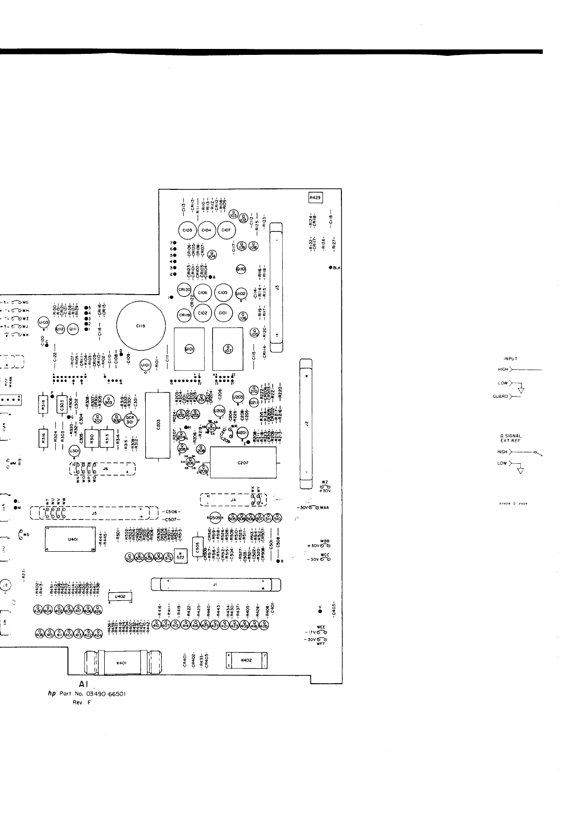
7a
6a
5a
4a
aa
za
@
+ö
r--l Te
f-l .ii .i
lliq;
tl
l-l
tl
l=l
tJ !.
n
l,l
L-J
INPUT
H|GH>-
Low> -.l
V
GUARO
>--
O SIGNAL
EXI REF
H|GH
>--\
rowh
V
c20t
aL
2."
D
I15
j
\7
I
ii
F>>, i-"---;--qq=l -
it;i
l-l'ooao- \'------qc!)
!-:((_6_6____:______.i_i
_iili_ "@.
oooooo
ä
gääsEFaF
Hää3$$g A Eä*$F$ifi
ä*än
I I
; :i:eeiyi qooi:fo ls | :ll:l:ttt trr: F
3 *rouFt,
@@@@@E
q4?FE$F$
qg*$Ht
I,!^ -..uüS
ffim
:- P
i ?
I $
{
$
ii+
P
f
gs I g
üä,ierispgglg*@ wEE
@(D@@@@@ ++++++++f++Evvvvvvvvvvvv _.:;R
eeag
tl
* ll
AI
lrp Port No.
0349O.66501
Rev F
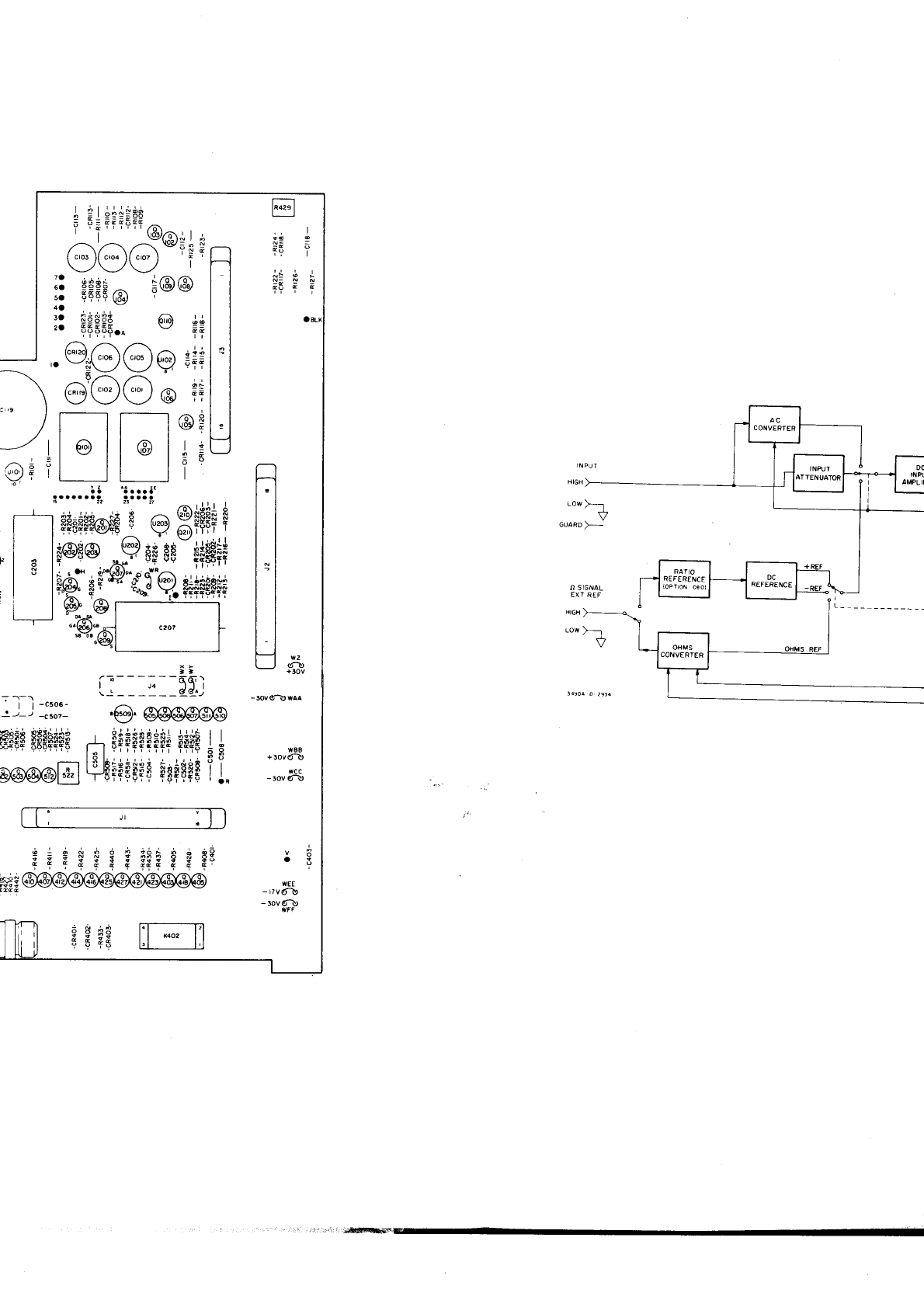
tR429 |
L-__l
r9
l5
l,i ö
EöG
fa
6a
5a
4a
ra
za
ii-
- -:--äii
.i-J -::ff- "@.
oooooo
#tF
tägn$fe
dr
E+Ff?F+P+
+i+t
lA
aoooE
t;4+qggqg
q$*$$t
Ii^
.IVC--oWAA
wa8
+5ovd-U
- 3ov
6\
m
;
i +
i i
{
f
+rr
l p
fs :
sf@ _,,.t:
*EfE
U
* 11
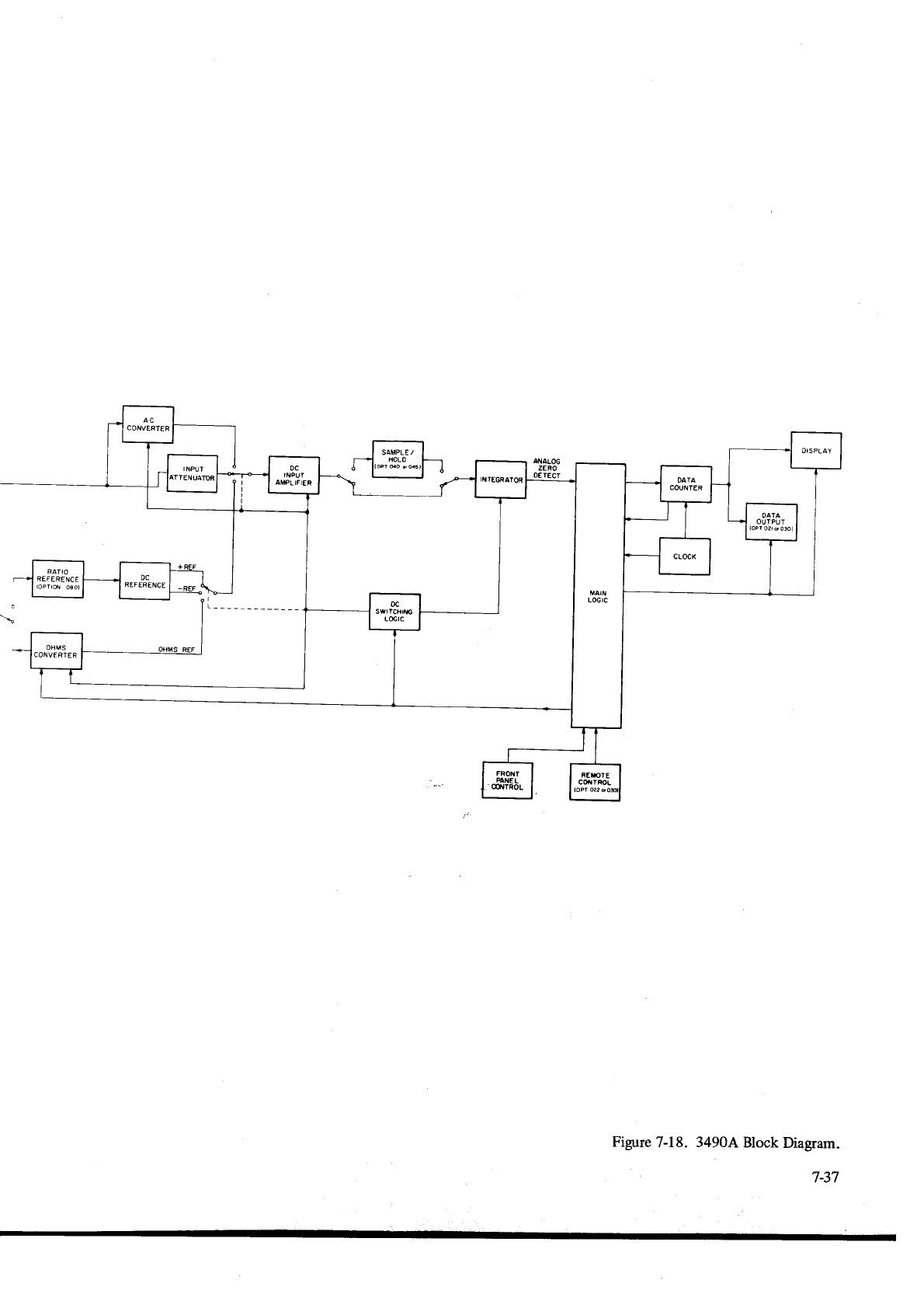
Figure
7-18. 3490A Block Diagram.
737
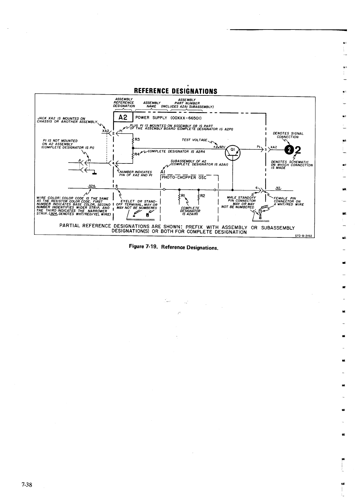
REFEBETTCE
DESIöTATIOtIS
Figure
7-19. Reference
Designations.
ASSEMALY ÄSSEA,'BLY
REFERENCE ÄSS€MALY PART NUMBER
OESIGNArION NAME UNCLUDES A2AI SUBASSEMELY)
PI IS NOT MOUNTEO
ON A2 ASSEMALY
(COMPLETE OESIGNATOR IS Pr)
r€Sf VOLTAGE
,.v.cOMPLEfE DEST6NATOR lS A2R4
? INDICATES
XAz AND PI
DENOTES SIGNAL
coKno^/
re2
t
7
OENOTES SCHEMATIC
?g #!lp, coNNEcrtoN
\
--i<<+---<
--<eL
qlR_E
9OLOR:
COLOR
COOE tS fHE SAME
As rHE REstsroa
coLoR
coDE.
FtRSr -
WüE:,Ä',li
L"^f,T Ff,
3
^i,',
fP ?fä,
3:'^'l
3
T_AE-
IH.IRD
tNDtcarEs
tne uaanöwea
srR t
p.
(e?3,
D€Nor
e s w urt aeot vtl win
e)
EyELET
oR saruo- |
OFF rERATINAL,MAY OR '
MAY NOT BE NUMSEREO I
l{{i I
SUEASSEMALY
OF
A2
///(CoMPLETE DESTGNArOR
tS A2At)
AI
Iexoro:cxoeeen
osc- -l
ll
RI
i
COMPLETE
DESIGNATOR
ts A2atRt
PARTIAL
REFERENCE
DESIGNATIONS
ARE
SHOWN:
PREFIX
WITH ASSEMBLY
OR SUBASSEMBLY
DESIGNATION(S)
OR BOTH
FOR
COMPLEiE'öESiEIrArrOrI
t
l
d
7-38
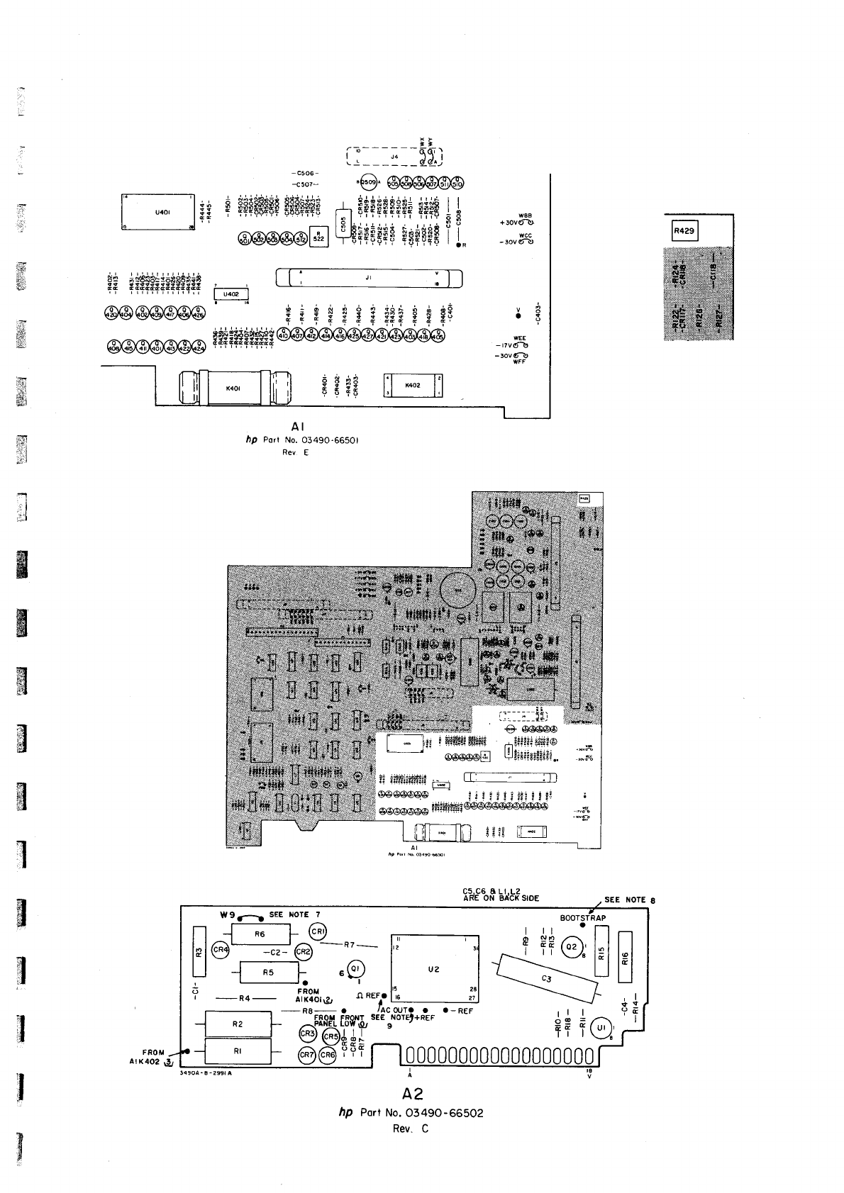
ti
i'---;--qq-l
.'------q.-ejj
-'lli- "@^@@@@@@
a
WEE
- rzvd!
- 5ov 6-l)
EsfE
[
*
n
"l
ä
ä
g
g
$
I
fl
hp Pott
No.
03490-66502
Rev.
C
l- *-]:s q
p?f8EFgfEäüFffä
* gf,?f$??*+
+++ü
JÄ w!8
r" -r.' @@@@@l.rl
lrh++rüql
le*s+c
Ti" l-;Ä
Bi;-r8iäiiäöäö*+B m
arelc?i.riiücai?tt'rll
,, L ua@.l
@@@@@@@
;
i?
$iF
i+P?
?
$ ?$
@6'@@@@ggfggg;s@
AI
äp Porl No. 0349O-66501
Rev E
c5.c6 a
Lr.L2
ARE ON BAC|( SIOE
w9r---t sEE roTE 7
lelQg -..-
@ -'l-
lJ -f ^.
l .9 I ,. I
i -ro- ilgt,,a ,,r.i.li. ,?l
-R8-a ,ACOUT?
a a-REF
I I FNOT FROI{T
SEE NOTET+REF
u::l- @öilr g'
{4 ööF$?f-looooooo
t-t
l.l
l-l
LI
s:
T
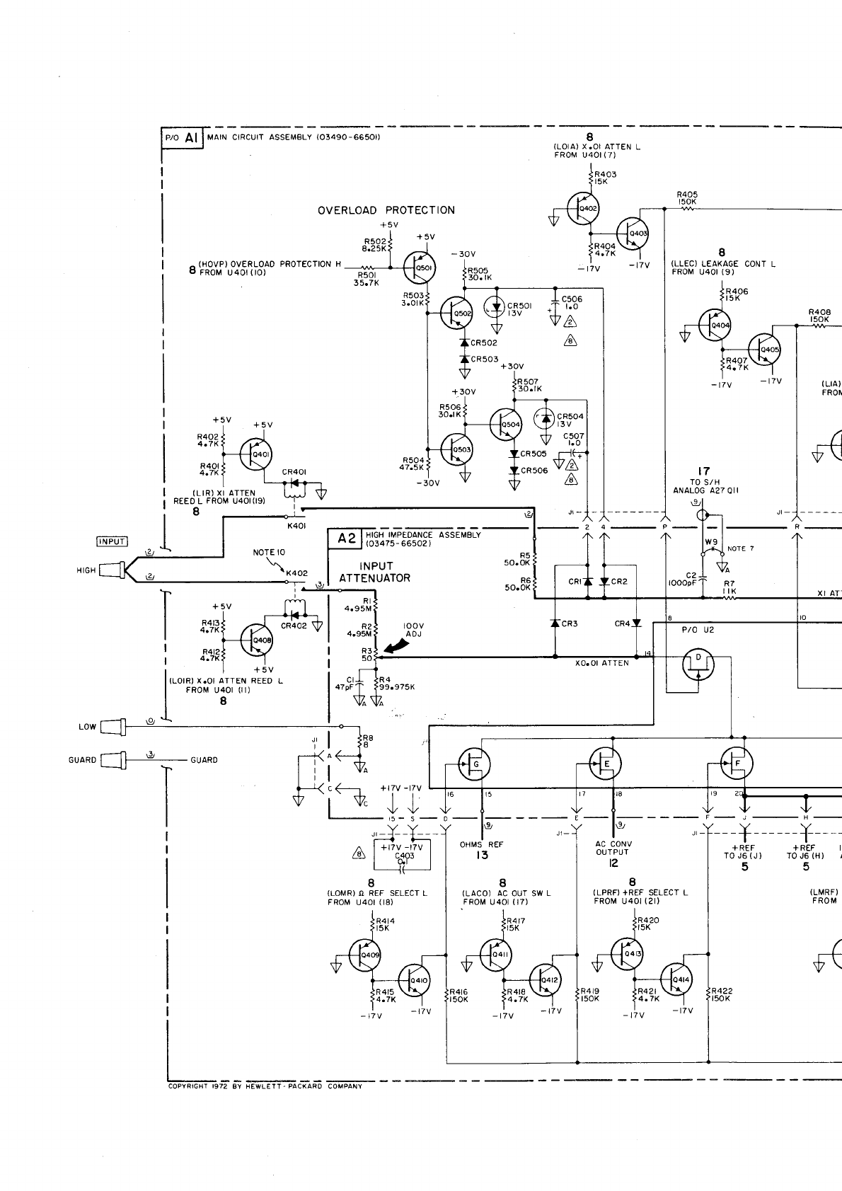
+t7v
-t7v
ll
lVcll
I Y-Y.
8
(LOMR)
O REF SELECT L
FROM U40t il8)
I
I
I
L-
I
{LOIA)
X.OI ATTEN L
FROM
U40t
{7)
OVERLOAD
PROTECTION
+5V
^ (HOVP)
OVERLOAO
PROTECTION
H
ö FRoM u4or ilo)
+5V
R402
4.7K
R40l
4.7K
(LIR)
XI ATTEN
REEO L FROM
U4OI(I9)
8
K3
50.oK
50.oK
IOOV
AOJ
t
I
I
I
I
l'''t
t
RI
4.95M
4
99.975K
-.11 \3,
GUARD
I Il-CUARO
-T
I
I
IVV
---T------1-----
+REF +REF I
TO J6
(J) TO J6
IH) I
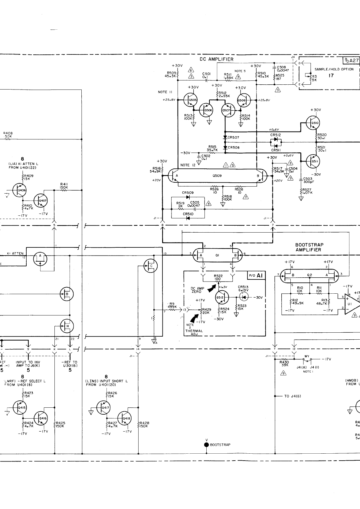
+30v
DC
AMPLIFIER -T6aztl
I
I
(HMDB)
/
FROM
IJ
c 508
o.oo47
R525
t87 R3 l7
5K
A
A
SAI\4PLE,/FIOLD OPTION I
R509
45.3K c 501
o.l
A
R408
5CK
I
{LIA) XI ATTEN L
FROM
U40t
(
22)
409
R4tO
4.7 K
,A - 30v
c503
30OpF
R4il
|
50K
2--J
K
-----1 wY
R430 l-l
1qk J4
(A) J4
(r)
/A NOTE I
l!\
R429
20K R524
t5K
I
I
I
I
I
;.. INPUT TO INV
I€ I) AMP TOJ6(K)
55
I
,LMRF) -REF SELECT
L
;ROM U40t
(8)
R423
t5K
I
(LTNS) INPUT
SHORT
L
FROM U40l (20)
R426
t5K TO J4(6)
/t
v\
22,
R4:
5.(
+
3OV "i' +3 OV
ruore rz
V AA
BOOTSTRAP
AMPLIFIER
Rr2 Rt3
49.9K 48.7K
-l7v - t7v
cR5r3
BOOTSTRAP
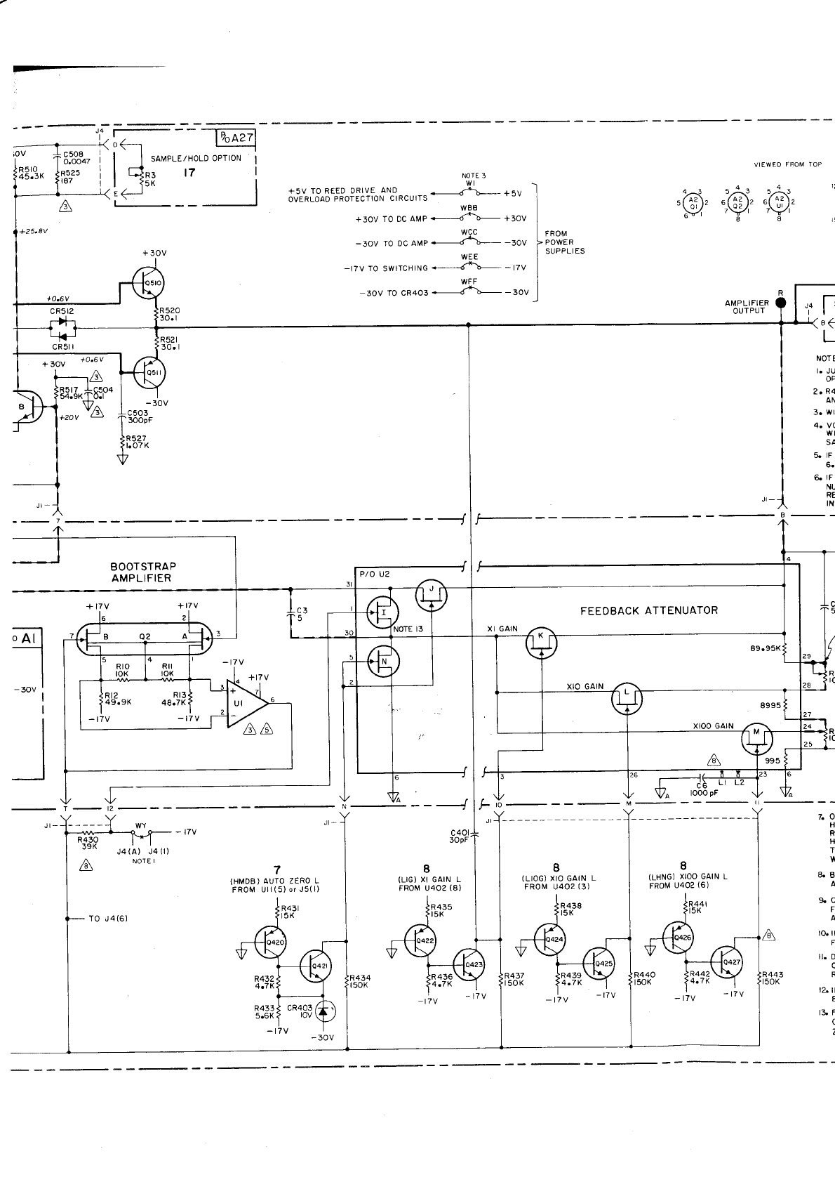
iov c
508
o.oo47
R525
187
+ 30v +a'6v
R5 t7
54.9K
+20v
SAIVPLE/HOLD
OPTION
R3 17
5K
+
30v
R5rO
45.3K
7-
NOTE 3
+5V TO REED
DRIVE
AND Ä ,..,
OVERLOAD
PROTECTION
CIRCUiTS
- -
WBB
+3OV TO OC
aMP
-_l-b- +3OV
wcc
-30v ro Dc at\4P d1 -30V
WEE
-l7V TO SWITCHING
+-*--J-*\-- - 17V
WFF
-3OV IO 66493 '-----J+b- - 36Y
X I GAIN
VIEWED FROM TOP
-4--4-t2
l,^J ),^J
e/l?)z
e(1-2)z
7\+l zV
8 I r:
4-<
'\ or /-
-\--.
A
FROM
POWER
SUPPL
I ES
ffPo
',A.
+ t7v
- 30v
.
c503
'3OOpF
R527
t.07K
BOOTSTRAP
AMPLIFIER
J4 (A) J4 il)
NOTE
I
AMPLIFIER
OUTPUT 'lr
B(
L
NOTE
r.
Ju
OP
2.
R4
AN
3o
Wl
wl
SA
6. rF
NU
IN
B
--
FEEDBACK
ATTENUATOR
'Ail
-
_*"1
I
I
__l
+t7 v
,,, vvva
to- M-
R430
39K
A7
(HMDB)
AUTO ZERO L
FROM
Ull
(5)
or J5{
l)
R43l
t5K
R432
4.7K
R433i CR4O3
5.6K > lov
c40l
3OPF
I
(LIG)
XI GAIN L
FROM U402 (8)
8
(LIOG)
XIO GAIN L
FROtlr U402 (3)
R439
4.7K
8
(LHNG)
XIOO GAIN L
FROM
U402 16)
7. ol
HI
R
tN
T
8. Bl
A
FI
to. tl
ILD
K
t2. il
raF
c
2
TO,J4{6)
- tlv - l7v
R437
|
50K
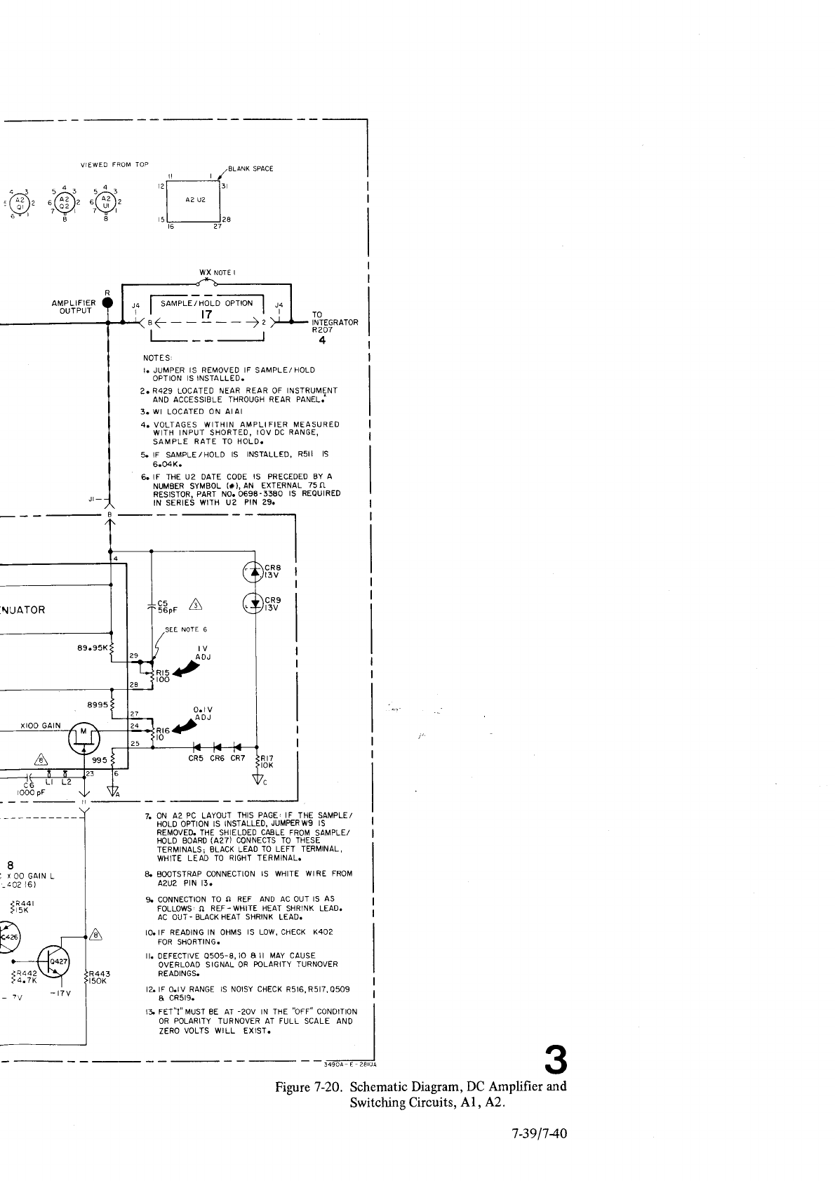
,ä, "tär;;
}7 'Y 'Y,
t | /'BLANK
sPAcE
,zl-----_l:
lozrzl
.tt^^
r4<ö
AMP LIFIER
OUTPUT TO
INTEGRATOR
R207
4
NOTE S,
I. JUMPER
IS REMOVED IF SAMPLE/HOLD
OPTION
IS INSTALLED.
2.R429 LOCATED NEAR REAR OF INSTRUIVENT
AND ACCESSIBLE THROUGH REAR PANEL."
3. WI LOCATED
ON AIAI
4. VOLIAGES wlTHlN Al\,lPLlFlER MEASURED
WITH INPUT SHORTED,
IOV DC
RANGE,
SAMPLE RATE TO HOLD.
5. IF SAMPLE/HOLD IS INSTALLED,
R5II IS
6. IF THE U2 DATE CODE
IS PRECEDED BY
A
NUMEER SYMBOL
(*),AN EXTERNAL
75N
RESTSToR,
PART NO.0698-3380 lS REQUIRED
IN SERIES
WITH U2 PIN 29.
$E?
O.lV
yt)""
X
CO GAIN L
4A? 16)
Z ON A2 PC LAYOUT TH|S PAGE, lF THE SAI\,IPLE,/
HOLD OPTION IS INSTALLED,
JUMPERW9 IS
REI\,IOVED. THE SHIELDED CABLE FROM SAMPLE/
HoLD
BoaRo
(A27)
coNNEcrs ro rHEsE
TERMINALS; BLACK LEAD TO LEFT TERMINAL'
WHITE LEAD TO RIGHT TERMINAL.
S. EOOTSTRAP
CONNECTION
IS WHITE WIRE FROM
A2U2 PIN I3.
$ CONNECTION
TO O REF AND AC OUT IS AS
FOLLOWS.O REF.WHITE HEAT SHRINK LEAD.
AC OUT.BLACKHEAT
SHRINK
LEAD.
IO.IF READING IN OHMS IS LOW. CHECK K4O2
FOR SHORTING.
il. oEFECTTVE 0505-8, lO A ll MAY CAUSE
OVERLOAD
SIGNAL OR POLARIIY TURNOV€R
READINGS.
I2. IF
O.IV RANGE IS NOISY
CHECK
R516.R517.Q5O9
a cR5r9.
IA FET,.T'' MUS1
BE AT
-zOV
IN IHE .,OFF.'
CONDITION
OR POLARITY IURNOVER AT FULL SCALE ANO
ZERO
VOLTS WtLL EXIST.
Figure
7-20. Schematic
Diagram,
DC Amplifier
Switching
Circuits,
Al , y'^2.
3
and
7-391740
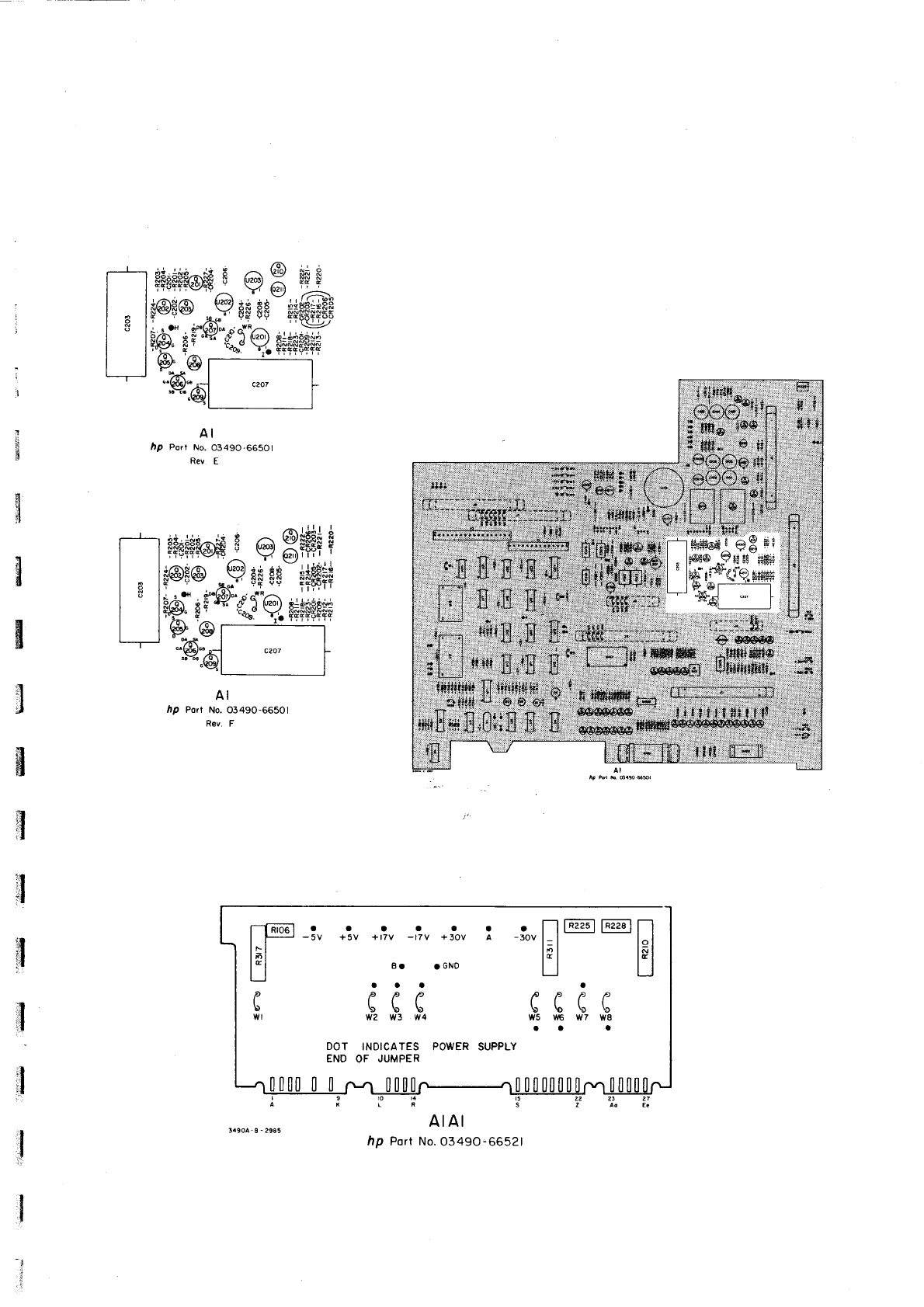
$rs*$roffia
C
I -A
ry@ü@
#sryns friW
äaf
r
il:$^onibD
*,i,r,+*nu
"H"
F: t"'v,i f+fry$ry++
p"@
..(ä# c?o7 f-
c?0f
AI
,lp Port No.
0349O-66501
Rev E
e
8+fE+
t
Ff
$$
**H++
,{9.
+*+pc+++
l^s H
qff"
'. 6ö
YY
. ,ä{.
,
F-8q/"i.,-
:i ,in
\€9y
I
ät:äsa^FÄ
HF+qSe4
*@$@
i,* *ö
@.pq*
@
@r
E.
pi
Ot 'z
9fs
":9"i
AI
,tp Port No. 0349O-66501
Rev. F
IRrr5-l FrrBll-l
--l.l
ldl
l"l
L_J
a
rf
5\)
w7 w8
o
PP
tl
D9
w5 \r,€
aa
DOT INDICATES POWER SUPPLY
END OF JUMPER
AI AI
hp Port
No.0349O-66521
czo1
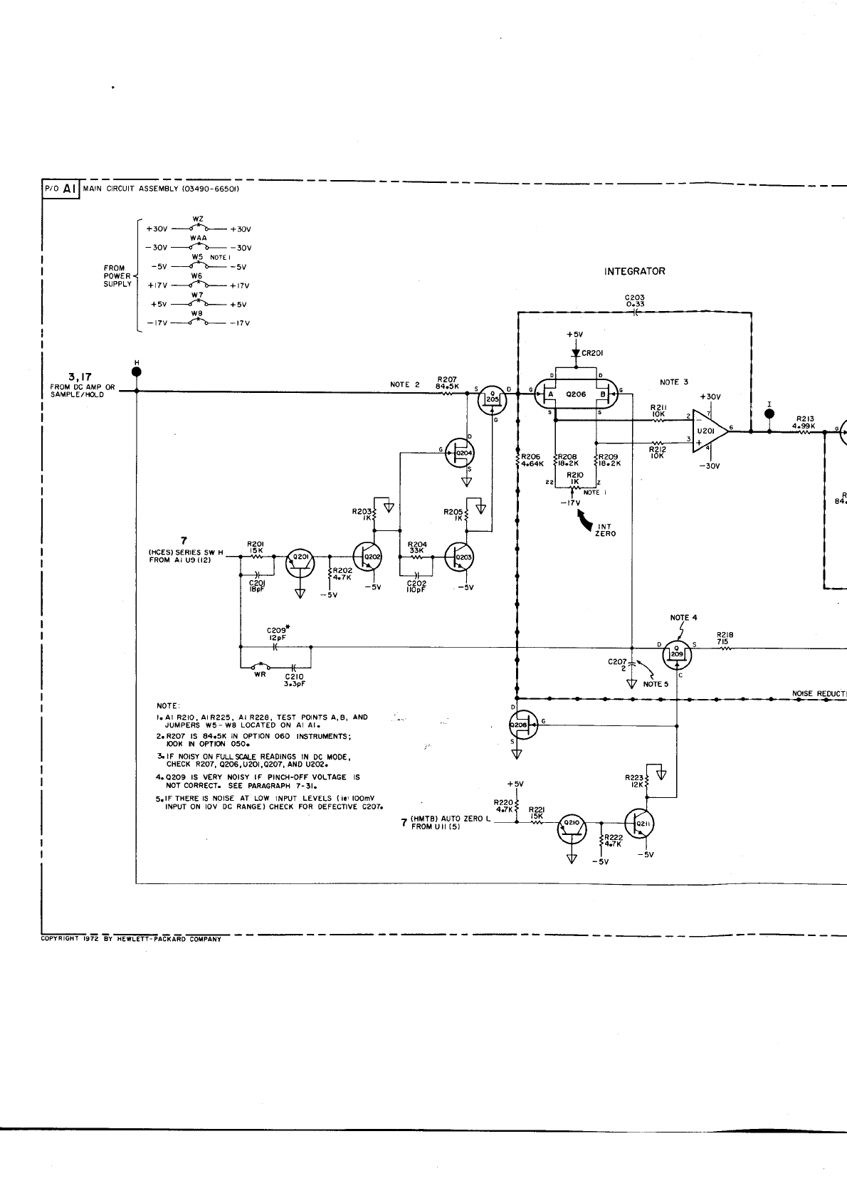
FRoM | -sv---<*-l---5v
POTVER < W6
SueeLv
| +rzV ----d-tr-E- +tzv
W5 NorEr
w7
+5V -----d-r-b-- +5v
w8
_tZV ___-<--b_ _tZV
7
(HCES)
SERIES SW
H
FROM AI U9
(I2)
3, t7
FROM DC AMP OR
SAMPLE/ IOLO
lp/0
Al I
MArN
crRcurr
assEMBLY
(o34so-6650r)
l-wz
| | +:ov ----a-r-r- +rov
IIWAA
| | -3ov ----d+-b- -3ov
c2to
3.3oF
NOTE:
I.AI R2IO,
AIR225, AI R228. TEST POINTS
A,8. AND
JUMPERS
IV5-W8 LOCATED
ON AI AI.
2.R2O7 IS 84O5K iN OPTION 060 INSTRUMENTS:
looK tN oPltot{ o50.
3.IF NOISY
ON
FULLSCAI-E R€ADINGS
ITI DC MODE.
CHECK R207,
0206, rj20r,0207, AND U202.
4.O2O9 IS VERY NOISY
IF PINCH.OFF VOLTAGE IS
NOT CORRECT. SEE PARAGRAPIT 7.3I.
s.IFTHERE
rS NOISE AT LOW INPUT LEVELS
(i.,lOOmV
INPUT ON IOV OC RANGE}
CHECK
FOR OEFECTIVE C2O7.
? (HMT8) AUTO
ZERO L
' FROM Uil {5)
tl
I
I
I=--
INTEGRATOR
c203
o.33
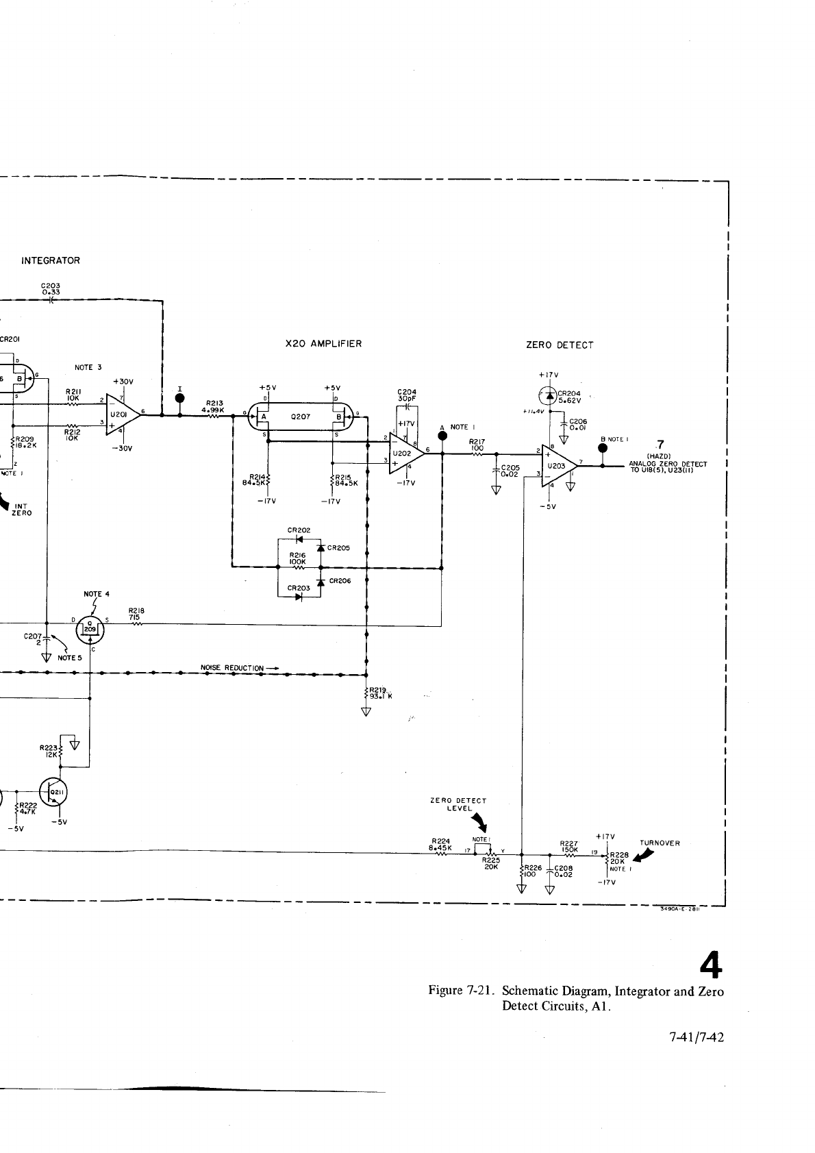
.t
ZERO DETECT
NOTE I
R2l7
too
l,
J-
STE I
\,*,"
TUR
NOVE
R
p
Figure
7-21. Schematic
Diagram, Integrator
and
Detect
Circuits.
Al .
4
Zero
ffi
,A?fli ffi
-t7v -t7v
cR202
1411742
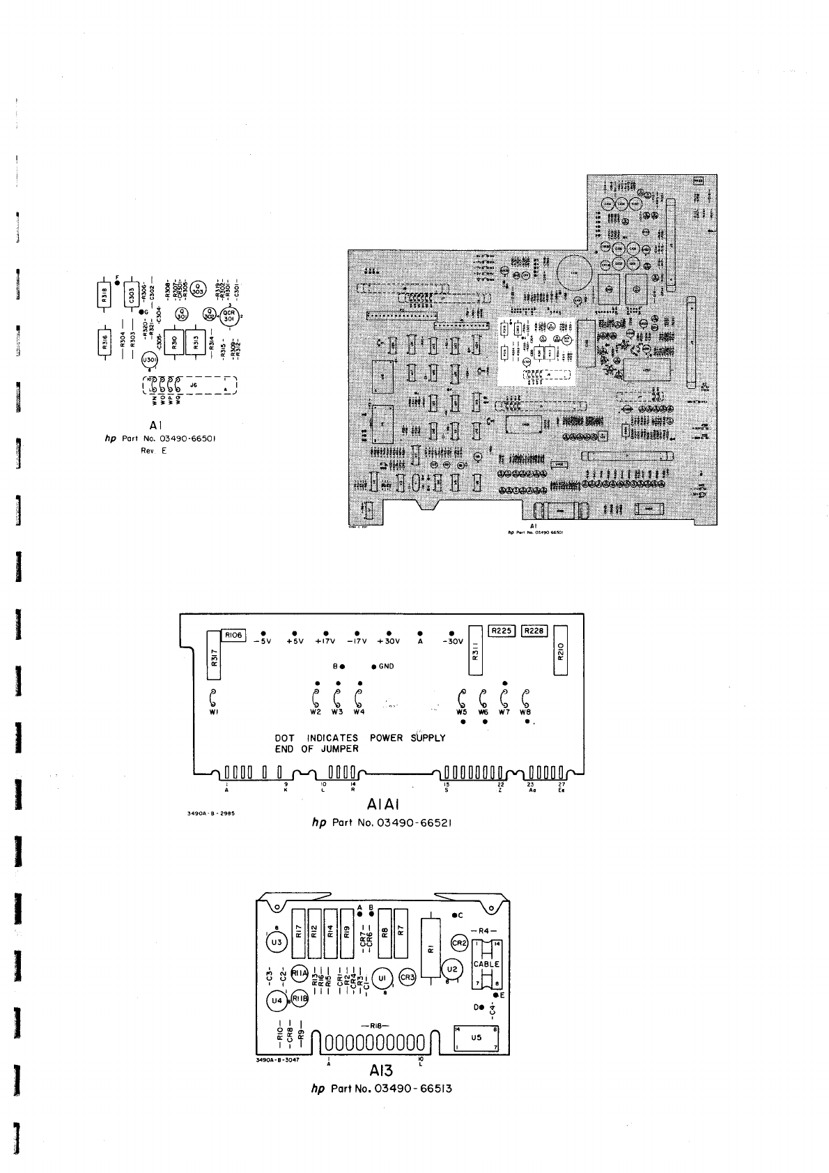
rtr
l;l
t"l
-T-
r\
l;l
t"l
*r
."-DE6rr-----l
r.
rblhb- l"- - -:-,1
.;:t
AI
äp Porr No.
0349o-66501
Rev E
. I Faq h-,,d
n
-3ov
l_l l"l
BE]
o
PPPP
tttt
b\D\f\'
W5 u/6 W7 wB
a a a.
aaaaaa
-5V +5V +r7V -r7V +30V A
B. . GNO
aaa
PPP
sbb
-
w2 w3 w4
DOT INOICATES
POWER
SUPPLY
END OF JUMPER
t-F@
lFl
LJ
?
D
3490A-B- 29A! AI AI
hp Port No.
03490-66521
-R4-
t-Tf,rl
I t--1 |
lcaBLE I
tHl
Lll-JjJ
.E
ood
öEEEE1iEE
I
xPf*trt*r+9e'
glw
I I | -Rr8-
TTfn0000000000
hp Port
No.
03490- 665t3
MArN
CTRCUTT ASSETVBLy
(03490-6650r)
NOTE I I
wr I
+sv--<a\](
tl
-^^-^^üll.
ru Jraö----i-i7
| (- +sv
RATIO REFERENCE ASSEMBLY OPTION
O8O (O349O.66513)
INPUT
PROTECTION
+17 v EXTERNAL REFERENCE
AMPLIFIE
lr
+rzv-{ 3
<-+r7v
ll
-rzv-{ o
<---r7v R2
27K ott,"t
{'itu
iä srcNar.l ril-i;r
IEXTREF | ry
t2 l
tt Ltf
""Z?-Jl
2
(F'
8\4{
76
B
I
cRl
t3.35V
cl
o.ool
€-----r
V^
ffieV
W2 NOTE I
l- *,zv ----<->-------. + | / v ro R3Or
, u3ot
(7)
I
FR.M I wl notl
9 PowER
i -l7v ------d b---l7V To u3ol
(4)
SUPPLY
I w4 NorE
I
| +sov ---=J*-b-+Jov lo R3o7
L
I
(LDFC)
RATIO L TO
DATA OUTPUT
t5
+Rl
NOT ES
I
I. R3II. R32O. AND JUMPERS WI-W4
LOCATED
ON
AIAI.
2. JUMPER WIRES WN-WO ARE
REMOVED
IF
RATIO
OPTION IS
INSTALLED.
PRINTED
CIRCUIT BOARD,-hp- PART NO.
O349O-66526
SUPPLIED WITH RATIO OPTION. MUST
BE
INSERTED IN J6 TO
MAKE THESE
CONNECTIONS
IN
ORDER
TO OPERATE
INSTRUMENT
WITH
RATIO ASSEMSLY REMOVED.
3. +REF.+REF
SENSE. AND
INPUT
TO INVERTING
AMP ALL
CONNECT TO SAME POINT ON
A2
(A2U2
PINzOL
4. tF rT ts NECESSARY TO REPLACE
OCR3OI,
R3O6,30S,3rO,
3I3,3I4, AND 3I5 MUST ALSO
BE REPLACED. THESE
MATCHED RESISTORS ARE SUPPLIED WITH THE
REPLACEMENT REFERENCE
OCR3OI.
5. IF UI IS NOISY, READINGS WILL 8E OUT OF
TOL€RANCE AT THE LOW END.
6. IF RATIO
BOARD IS PUTTING READING INTO
OVERLOAD,
REPLACE
U5.
+ t7v
INPUT
COMPENSATION
AMPLIFIER
76K
12 lov I w8
l?-rv
_l !- pt ( .
Lii
c30l
o.l
copy R ,GHT | 97 2 By H EwL ETT
- pa-cxm-oTrplnv-
: AMPLIFIER
REFERENCE
POLARITY
LOGIC
D
/^"'i;;'
\y \y
+ REFINPUI
INPU'T
+REFERENCE
SUPPLY
R3t6
to.oK
INVERTING
AMPLIFIER
F
R3r7
20
NOTE I
a
I
-REF
R3
t3
2.662K
R3t4*
200
R3t5+
50
- REF
INPUT
T
FROIV
J
+REF S
FROI\4 J I
wo
NOTE
Figr
LOW FOR
+ REF INPUT
REFERENCE
POLARITY
LOCIC
cR8
4.75V
{
TOP
VrEW)
(HRAP)
RAT|O POL TO At
U40t
(27) 8
THRU
S,/H
OPTION
I8
WN NOTE
2
(H
IN
P)
INPUT
POL FROM AIU22(8J 7
HIGH FOR + INPUT
LOW FOR - INPUT
J6
I
: FOR INT
-t
I
w8 |
-ll
---------r6
AI
U30
at3
ut- 4
a
,'^'.
-.\-/.-
\Z \Y
K-9
-REF
roJr(L)
l
INPUT
TO IIIVERTING
AMP I
FROM
Jr
(9) I
la
+
REF
SENSE I ^---
rcorv
Jrlal
I
sEr NorE
3
+ REF
r0 Jt
(J) )
INVERTING
AMPLIFIER
, I u3o! ->---t-
io':l-.1*1' *5#3
R
5
Ratio
Figure
7-22. Schematic Dagram, Reference
and
Circuits, A1, A13.
7431744
-5V g-l)wc
+ 17V
C-t) Wx
4az | -17v6-DwI
aaaa +sv(t-!rwJ
f o--trwx
a--;- -- --- l-f
lt rstl
\-!:-- _---:)-J
a-'^iDa-DZ 2 -T r-\
| | (((t,{r Jt I r
r-u------J99 ---- ß
t-'
3;;-t'
N'
,.1
i
oa
P'
oa
T_l'
I laL
lil r*
l-l
dl
fi
l.l
l=l
,l l-
.X
T-T
l-l
"fT
l'l
.L_t 'n'
l'l
[u8,
v
"r1"
ll
I'l
tl
!|J-
AI
tlp Port No. 0349O'66501
:;.: .;ä:,
9sö$! ( *
i: ':';ß?;;i-:,-
----, , *1
*$1,sE1i;V
F.---*-a ..;e!i :t:''i,t"",. l
,iä:r
?ääij'O
FffiilHffiffi:tr
r. r .-.
__,-ii.
';";
! .ll l:lt
ri.ä-i.i::. i:: ;:j ' 'o,ffi
-.1 :- [---. lli |@S*E oirrr:r:*l*o
;'l r',u,
E '[ E' I '*
-rrr
-ä*,ä nil;;;'ilji
i:sri:iii;:f.l'iir.:i;i...
Ot ---1;_lr,
5!::!i: .L o e o- i3
ritsiirifrs?
,= 5 _ -
Tl fi .::.r .n fl @@O@O i ii }i i i iiS
i: !r
.'i.ä
lf ..i !.U., [ ü ü **r6*tsWi#i@o@o@€mo,om
,."8
.E
*.E
+E
,.E
ll"n"
| | l:l
l-l "L-r
tl
a
LETTEA
SAOWN BESIDE
GFOUND SYMBOL ON
SCHEMATIC
INOICATES
JUMPEF WI FE
OESIGNATION
JUMPERS MAY 8E AEMOVED
DURING TBOUBLESHOOTING
TO ISOLATE
INOICATED POB
TlONS OF THE
CI
BCUI T
GROUND CIACUIT JUMPER WIB€S ON MAIN CIRCUIT ASSEMBLY A1
Rev E
3
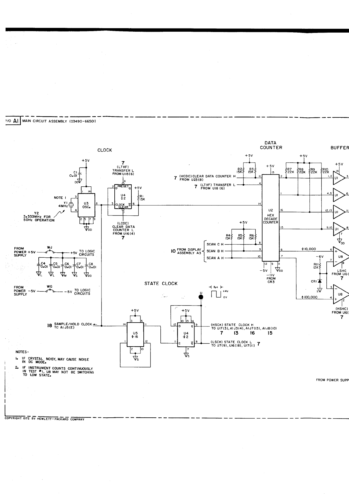
,/o Al I MArN
ctRcurT
assEMBLy
(o349o-665ot)
CLOCK
DATA
COUNTER
+5V
o.ol
NOTE I
4Mi;Q
7
(
LTXF)
TRANSFER
L
FROM
UI8(6) (HCDC)
CLEAR DATA COUNTER
FROM
U23(8)
? (LTXF)
TRANSFER
r FROM
Ut8
(6)
3.333[iz FoR
/\/
5OHz
OPERATTON (LCDC)
CLEAR OATA
COUNTER L
FROM
UI6
(4)
7
+5V
FROM
POWER +5V
SUPPLY
NOTES,
t. rF
IN
LIF
IN
TO
l-r.o*
. "
n i!g!"?if'iJj scaN B H
LscaN
a H
LSHC
FROM
U6(
7
U8
U8
STATE CLOCK
FROM
POWER
SUPPLY
-5v
---dä-!-- -" IP*33|]3
GRYSTAL
.NO|SY,
MAY
CAIJSE
NOrsE
INSTFUMENT
COUNTS
CONTINIJOUSLY
TEST 'I, U8 MAY NOT 8E s,I/ITCHING
LOW
STATE.
-1 8/s l-
T-.] | * ou
lLlov
(HSCX)
STATE
CLOCK
H
TO
U17(3),Ar J3(4),
Ar
J7il3), Ar J80O)
71316t5
(LSCK)
STATE CLOCK
L a
TO
U7(9), U16il8), U17(il)
r
(
HSHC
)
FROM
U6(l
7
FROM
POWER
SUPP
I
I
I
coLFf üa;ir6?tdiffffi FicaRDöo-iim-i-
Rtl
tzK
cRr
,
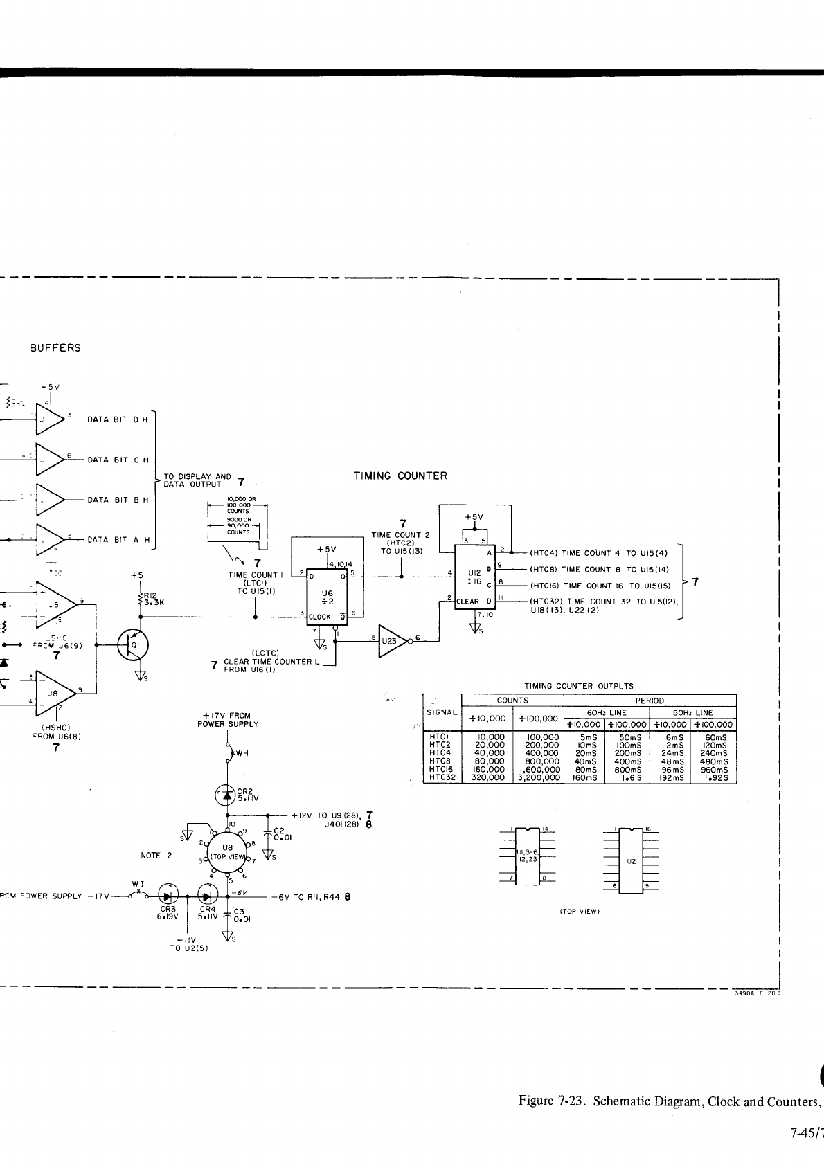
3U
FFERS
DATA
BIT O H
OATA BIT C H
.\
. ,>- DATA BIT B H
'r./
>.- :ATA BIT A H
L/
TO OISPLAY
AND ,
DATA OUTPUT J
. to,@oF
F- rm,@ --i
I c@{rs I
I $@OR I
l._ eo,ooo
--l I
I couNrs | |
--\------lJ
\\7
TIME
COUNT
I
(LTCr)
TO Ut5il)
TIMING
COUNTER
7
TIME
COUNT 2
(HTC2)
TO
Ut5(t3) (Hrc4)
TrME COUNT 4 TO ',a,O' I
(Hrcs)
.ME couNr
8 ro ur5a4) |
(Hrcr6)
T'ME couNT 16 To
ur5rs) | ?
(Hrc3z)
TIME
couNr 32 ro urstrzt,
I
ur8il3).
u22
(2) )
t
H
-
r
(
LCrC)
7 CLEAR TIME
COUNTER L
I FROM
Ut6
(
t)
+ I7V FROM
POWER SUPPLY
+r2v To u9(28),
7
u40t
(28)
g
-6V TO Ril,R44
I
TIMING COUNTER
OUTPUTS
s
io
r'ra
rCOUNTS PERIOD
+
ro,ooo +roo.ooo 6OHz LINE sOHz LINE
* to,ooo+
roo,ooo
+ro,ooo+
roo,ooo
HTC I
Hr.c2
HTC4
HTCS
HTC I6
HTC32
ro,ooo
20,ooo
40,ooo
80,ooo
r60,ooo
320.OOO
roo,ooo
200,ooo
400,ooo
800,ooo
r,600,ooo
3,200,ooo
5mS
l0mS
2OmS
40mS
EOhS
l6OmS
IOOmS
2OOmS
4OOmS
SOOmS
r.6 s
l2mS
24mS
48 mS
96
mS
192
mS
6OnS
l20mS
24OmS
480mS
95OmS
t.92S
I
Figure
7-23. Schematic Diagram,
Clock
and Counters,
7451-t
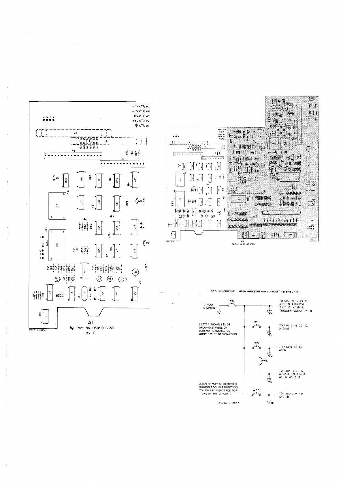
4f,2 |
aaaa
- 5v c.lJ wc
+t7v(t-\)wH
-t7v
6\wr
+5v 6!wJ
$<ruwx
I ä
,t*
U F S.i
,..,8
.E-,E
+E
,.E
Tt"
lql
I'l
tl
.X
TI
l-l
i'n'
l'l
(u8)
v
EGROUNO
CIBCUIT JUMPER WIRES
ON MAIN CIRCUIT ASS€MBLY
A1
AI
Itp Porl No.
O349O 66501 LETTEA
SHOWN BESIOE
GROUND
SYMEOL ON
rcHEMATIC
INDICATES
JUMPER
WI RE DESIGNATION
JUMPEAS MAY B€ R€MOVED
DURING TBOUBL€SHOOTING
TO
ISOLATE INOICATEO POR
TIONS
OF THE CIRCUIT.
TO AlUt.9. 19.23.24
atPl
(7t.
arP2
05).
ArJT
fi5)
A1J8{l8l
TRIG6ER ISOLATION
14I
TO AlUl6 18.20
22i
ar
c4. 5
TO A1Ur0. r3 15.
arc6
ro
Atu4 8.
r r, 12.
atc2.3.7
9.
ATCRJ.
41814, ArOr 3
TO
AlU2.3r A1R34j
A1C1.8
'rT -ft^
t-tt-l
l;l lrl
tt 8tl
!U. !U
.J
rrl r "f-I
g;ls
s l-l
r"rl-l
?H'ä$
i r,
"i t+*truuiit!
frffiffi
i3{{g:.:_i
ä;i;iiir;r:
]l'ir:,:';i"';l ..1
i
*i:lir -! o @ @,
=
T-T
r,r,:
ll
p .L.i"U:;
11
.B I
stir lT
- Il
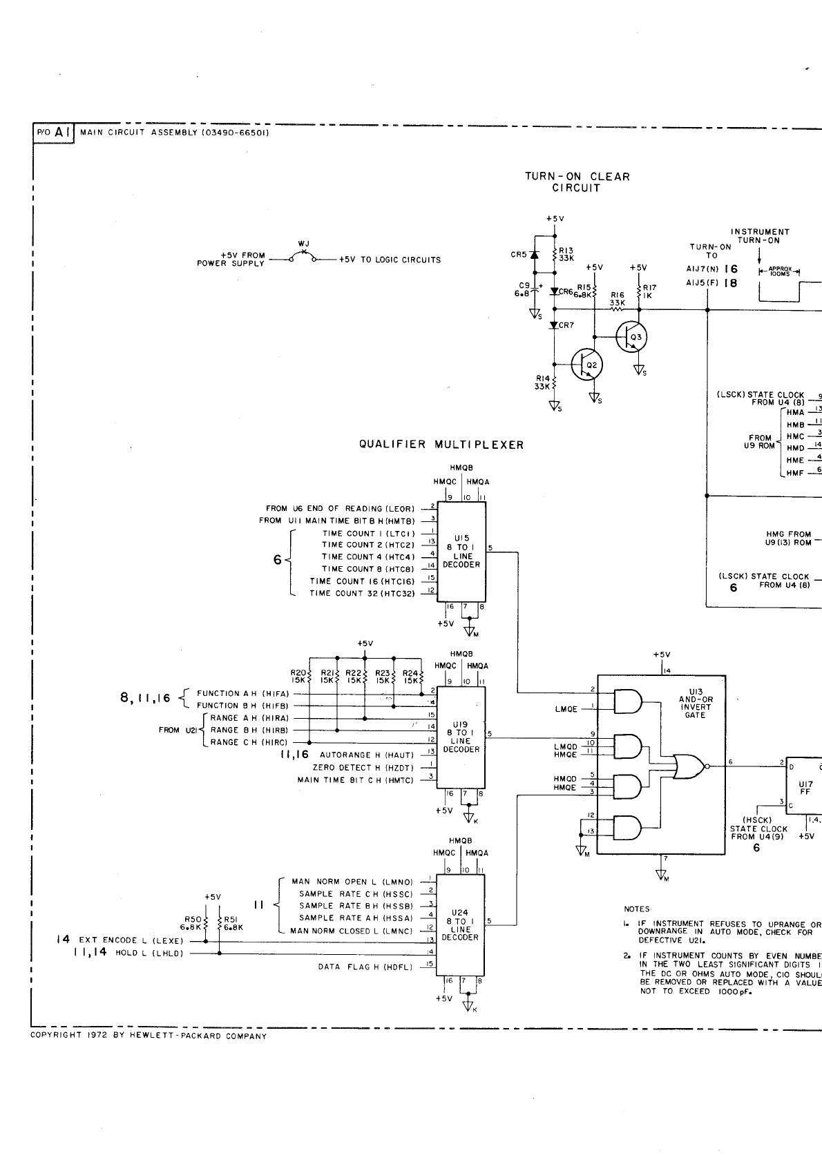
MArN CTRCUTT ASSEMBLy
(O3490-6650t)
TURN
-
ON CLEAR
CIRCUIT
WJ
+5V FROM ,"\
poweä-su.pplV < ö-+5V TO
LOGTC
C|RCUtTS
I N
STRUME NT
TURN
-ON
T URN.
ON I
TOI
I
AIJT(N)
AIJ5
(F) l.-i3Bl,"J-r
L__J-
QUALIFIER MULTI
PLEXER
HMOE
HMQC I HMQA
(LSCK)
STATE CLOCK s
FROM
U4 (8) --:
l-rua
--'t-:
I xma
--!
FROM -J HMC
-
us RoMl Hr4e
_-11
I nne
--r
LHur
---q'
FROM
I,J6
ENO OF READING
(LEOR)
FROM
UI I MAIN TIME
8IT
B H
(HMTB)
r IME COUNI
| (LTCI
)
I TtME
COUNT 2
(HTCz)
61 rlMEcouNr4(Hrc4)
I TrME
COUNT
8 (HTC8)
I rrue
couNr
r6(HTcr6)
I
L TIME
COUNT
32
(HTC32}
HIFA)
-
HtFE)
-
HIRA)-
H
tR8)
-
HrRC)
-
il,
[- MAN NORM
oPEN L (LMNO)
I SAMPLE RAIE C
H {HSSC)
ll < saMPLE RATL
BH (HSsBl
I
R5t I SAMPLERATEAH(HSSA)
6.8K L l,rltt ronu cLosED L (LMNc)
HMG FROM
u9
il3) ROM
-
(LSCK}
STATE CLOCK
_
5 FRoM
ua (8)
8,rr,re
{
FROM
U2I
R50
6.8 K
FUNCTION A H (
FUNCTION
B H (
l'naHcr
a x t
1 RANGE
8H (
LRANGE
C
H
(
l6 auroRANGE
H
(HAUr)
ZERO
DETECT H
(HZDT)
MAIN
TIME 8IT C H (HMTC)
LMQD
HMOE
HMOO
HMOE
+5V (HSCK)
STATE
CLOCK
FROM
U4(9)
6
|.4.
+5V
HMOB
HMOC
I HMoA
l4 exr ENcoDE
L
(LEXE)
ll,l4 xor-oL(LHLo)
NOTES.
I. IF INSTRUMENT
REFUSES
TO UPRANGE
OR
DOWNRANGE IN AUTO
MODE. CHECK
FOR
DEF€CTIVE
U2I.
2. IF INSTRUMENT
COUNTS
BY EVEN
NUMBE
IN THE TWO LEAST SIGNIFICANT
DIGITS II
THE
0c OR
OHMS
AUTO MODE,
CtO SHOULT
8E REMOVEO
OR REPLACED
WITH A VALUE
NOT TO EXCEED
lOOOpF.
L
COPYRIGHT 197? 8Y HEWLETT.PACKARD
COMPANY
DATA FLAG H (HOFL)
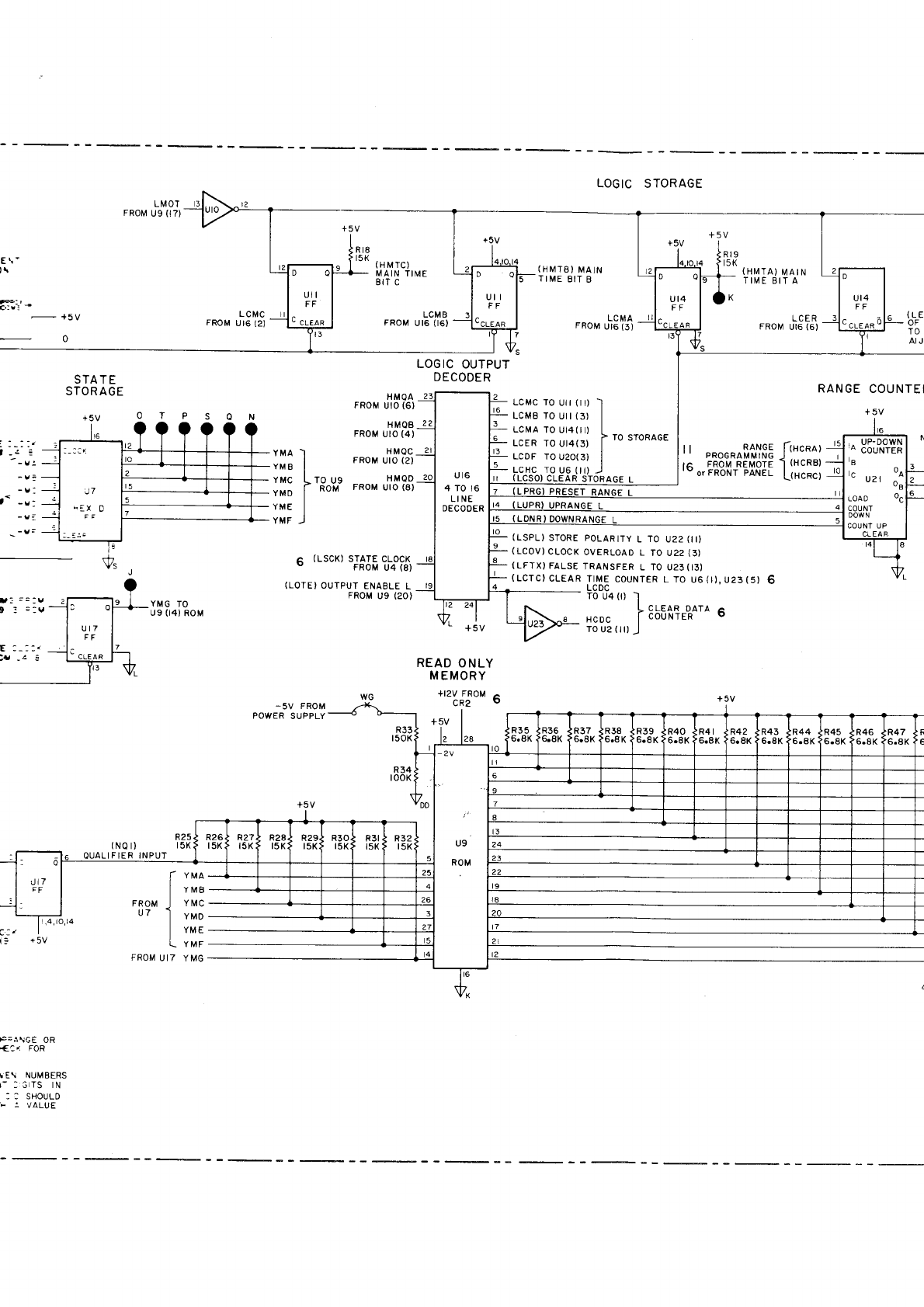
LOGIC
STORAGE
(
H MTC)
MAIN TII\4E
BIT C
LCM B
FROM Ut6 fl6)
(HMTA)
MAIN
TIME BIT A
,^ UP-DOWN
'^ COUNTER
ta
,^ o^
'' u2i ^^
LoaD oc
COU
NT
DOWN
COUNT UP
CLEAR
E\- (HMTB)
MAIN
TIME
8IT
B
LCMA
FROM
U16
(3)
LCMC
FROM UI6 12)
LOGIC
OUTPUT
DECODER RANGE
COUNTE'
+5V
HMQA
FROM
UIO
(6}
HMQB
FROM
UIO
(4)
HMQC
FROM UIO
(2)
HMQD
FROM UtO
(8)
STATE
STORAGE
+5V
11 RANGE l-lirCaat
. . PROGRAMMING
I
IA FROM
REMOTE I (HCRB)
,- or
FRONT PANEL L(HCRC)
STORAGE
L
l-
TO Uil (il)
TO
Uil
(3)
TO Ur4
{
il)
TO
Ut4(3)
TO
U20(3)
ro u6
0t)
CLEAR S'
LCMC
LCMB
LCMA
LCDF
POLARITY
L TO
U22
(II)
OVERLOAD
L TO U22
(3)
TRANSFER
L TO U23(13)
T]ME
COUNTER
L TO
U6(I),U23(5}
6
ro
u4
(r)
Ii 3bEi,?#'^
e
röüä
rrrr
-l
(LSPL) STORE
(LCOV)
CLOCK
(
LFTX) FALSE
(LCTC} CLEAR
YMA
I
YM8 |
YMC I TO
U9
vr.,lo
I RoM
YME
I
YMF J
a
A (LSCK)
STATE CLOCK
- FROM
U4
(8)
(LOTE}
OUTPUT
ENABLE
L
FROM
U9
(20)
2
YMG
TO
u9
04)
ROM
+5V
READ
ONLY
MEMORY
+I2V
FROM
^
cR2 o
(N0
t)
QUALIFIER
INPUT
l- YMA
I YMB
FRoM I Y l\'lc
u7 1 vr,,to
I trt
I
L YMF
FROM
UI7 YMG
F-A\GE OR
ta( FoR
rE\ NUMBERS
r-:3TS lN
: : SHOULO
; : VALUE
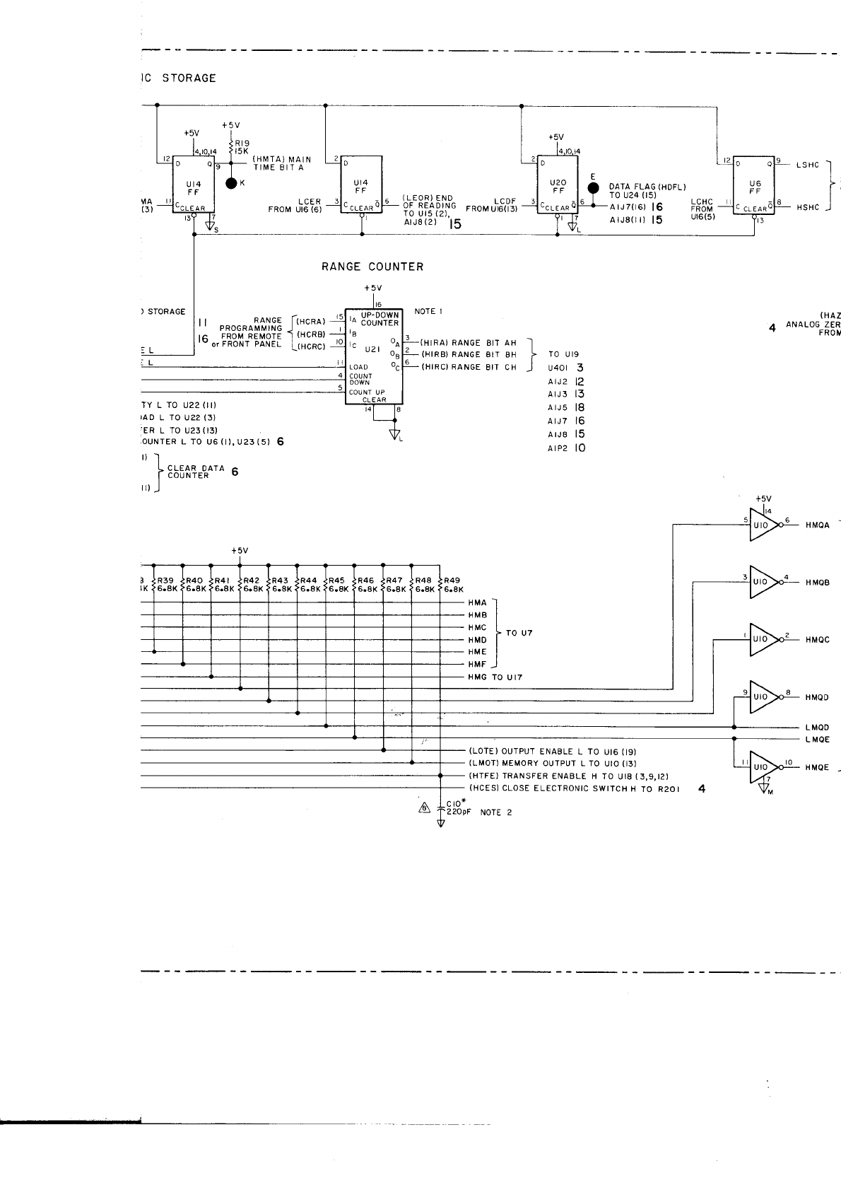
I <Rtg
la.ro.r4 ?
l5K
12r^--------:l I (HMTA)
MAtN
Tll\,lE
BIT A
K
LCER
FROt\,t
Ut6 (6)
. (LEoR)
END r .nF
- ?5 Sili;j:. FRoMU''6iIä)
ArJs(2)
l5
OATA FLAG
(HDFL)
TO
U24 ils) LCHC
'F--.-ArJ7(16) l6 Fäöü
I arualrrl
15 ul6(5)
IC STORAGE
RANGE COUNTER
+5V
4 o*otonrä5[i
",)
BrE**#'^
.
TO
U19
u4or
3
atJ2
l?
nru:
l3
at,.rs
l8
ar,rz
16
rrJe
l5
nrpz
lO
(LOTE)
OUTPUT
ENAELE
L TO
UI6
(I9)
(LMOT}
MEMORY
OUTPUT L IO UIO
(13)
(HTFE)
TRANSFER
ENABLE
H TO
UI8
(3,9,12)
(HCE5)
CLOSE
ELECTRONIC
SWITCH
H TO R20I
HMA
I
rua
I
t"t I to ut
HMD
I
HME
I
HMF
-J
HMG
TO
U 17
," uP-D0wN
'A COUNTER
iB
t ,r, lo
LoaD oc
COU NT
DOWN
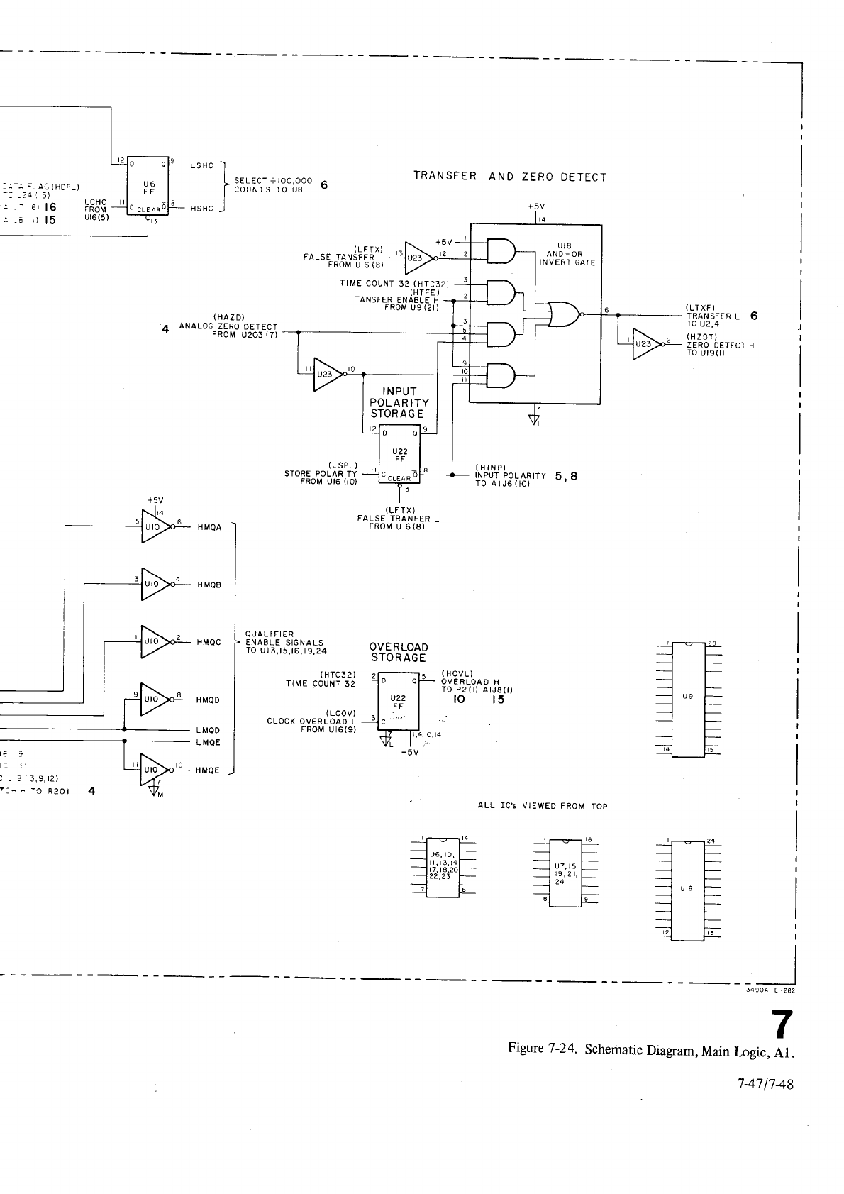
LS HC TRANSFER
AND
ZERO
DETECT
+5V
(HAZD)
ANALOG
ZERO
DETECT
FROM
U203
(7)
HMQC
(
LTXF)
rnarusrER
L 6
ro
u?,4
(HZDT)
ZERO OETECT
H
TO
ut9fl)
OUALI FIER
ENABLE
SIGNALS ^r
iöi,liisliä)31,"q 3Yä1.^.dP
(HTC32)
TIME COUNT
32
(
LCOV)
CLOCK
OVERLOAD
L
FROM
UI6(9)
ALL IC's
Vl€WED
FROM
TOp
ut8
AND
-
OR
INVERT
GATE
INPUT
POLAR
ITY
STORAG
E
IIME
COUNT
32
(HTC32)
(HTFE
)
TANSFER
ENABLE
H
FROM
U9
(2I)
3l8'd',tshäl'"
5'8
3,9,
t2)
rc R20
|
i
_l
*""^;'
Figure
7-24. Schematic
Diagram,
Main
Logic,
Al.
7471.748
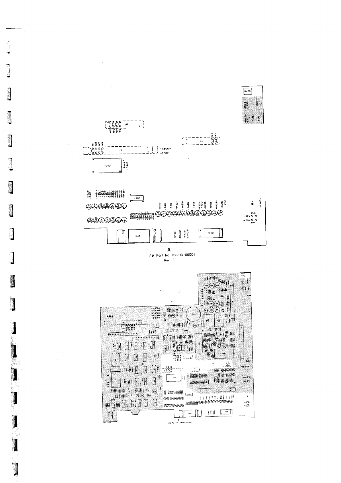
{
a1
.t
ru1
ä
.!t
:,*l
'J
il
;J
-l
.J
g
ä
,]
:3
ä
3
3
il
t:..
1'
,ä
;
ä
I
g
,ä
^tbEiJf - - - - -i
I i-{-( | JG I
i'
'bEsD !-t
;3C9
-_ _, ,_t:_
i ,,PP?P J5 i t-c5o6-
'1 q\t_b_b_s_ _-:r-) -c5o?-
;.
.-.------o-d;]
I J4 )ä,1
\i------=--l
@@@@@@
@@@@@@@
I u40z I
i------- e = e N n ä e säü a t gg
; E
: r E
i i +{+
{ i +'
pp*
*späsw:
@@@@@@@@@@@@
esie
ff
* n
F R ür lrl l,l
n
1=1,
l-1,
il
**.
*=_,
;
.'":
''Y^
:
$'g)
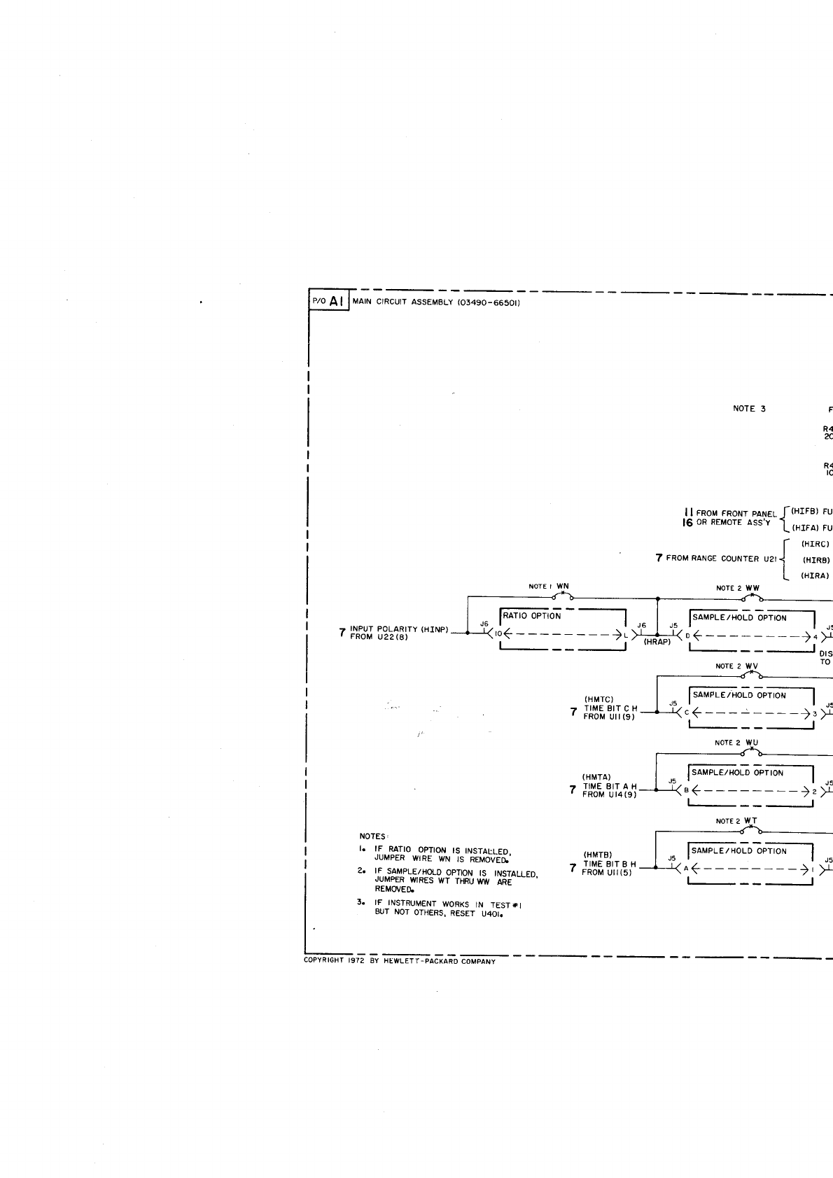
i' a;
|"*;,,ilJ**io**l.Io,l
r
I
I
NOTE
3
NOT€
2 IVW
R4
&
R4
to
I I rao, rnotr paNEL
f(HrFB) FUI
16
oR REMoTE
o.s', t ("rrot ru,
[- (HrRc
)
Z FRoM
RANGE
coultrea uzr
J (HrRB)
I
L (HIRA}
NoTE I WN
7 |NPUT
POLARTTY
(HINP)
' FROM
U22(8)
NOTES.
r. t,1..11r_ro..ol]roN
ts tNsrALLEo,
JUMPER
WIRE
WN IS REMOVEI'
2. IF,.STi,PLE/HOLD
OPTION
IS INSTALLED,
JUMPER
WIRES
WT THRU
WW ARE
REMOYES
3. IF INSTRUMENT
WORKS
IN TEST*I
BUT
NOT
OTHERS,
RESET U4OI.
ISAMPLE/HoLD
oploN I
, I r:
o(-- --)"X
I
(HMTC)
7 T|ME
BtT
C
H
' FROM
Uil
(9)
(HMTA)
7 TIME
BIT A H
' FROM
Ut4(9)
(HMTB)
? T|ME
8tT
B H
, FROM
Uil(5)
,. lffioi
,, [**6'ffi-l ,.
{.(---:----).F
NoTE 2 WT
o fää-.trto-*;t'ot -l
COPYRIGHT
1972 BY HEWLETT-PACKARD
COMPANY
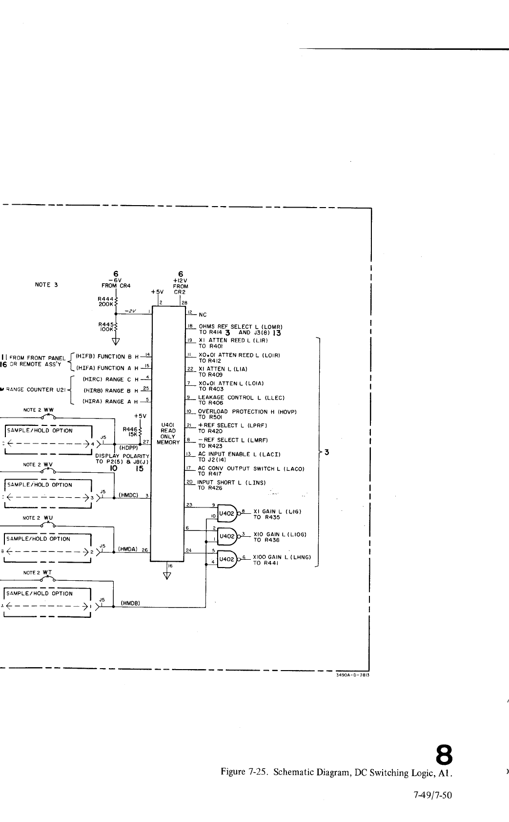
6
-6V
FROM
CR4
I
R444
<
200K
i
6
+tzv
FROM
cR2
2a
_ - -J DISPLÄY
NOTE
2 WV TO P2(5)
NC
OHMS REF
SELECT L (LOMR)
ro R4t4 3 aND J3(8) 13
XI ATTEN REED
L (LIR)
ro R40l
XO.OI
ATTEN
REEO
L (LOIR)
fo R4l2
XI ATTEN
L (LIA)
TO R409
XO.OI ATTEN
L (LOIA)
TO
R403
LEAKAGE
CONTROL
L (LLEC)
ro R406
OVERLOAD
PROTECTION
H (HOVP)
T0 R50l
+REF
SELECT
L (LPRF)
ro R420
-REF SELECT
L (LMRF)
TO R423
AC
INPUT
ENAELE
L (LACI)
TO J2il4)
AC
CONV
OUTPUT
SWITCH
L (LACO)
TO
R4t7
INPUT
SHORT
L (LINS)
TO R426
(
r_.lc
)
R445
tooK
POLARITY
a J8(J
)
t5
[--soue.e,."oloieftil-l
:(---'----).
f
-sarrPLE^1oLDörlöil-l
rl
: ( - ----- -- )z
NoTE 2 WT
[-soupr-Ezro-r-oirfr
'-l
r(-- --)r
XIO
GAIN
L
(LIOG)
TO R438
XIOO
GAIN L
(LHNG)
TO R44l
XI GAIN L
TO R435
Figure
7-25. Schematic
Diagram,
DC Switching
Logic,
I
A1. )wer
Supplies,
A l,
(
t
I I .Rou
raotr ro*aa [-{Hrra) FuNcrtoN
B H
16
cR REMoTE oss'Y f tnrmt FuNcroN
A H
f (HrRc)
RANGE
c H
I
y ?aNG5
COUNTER
U2tl (HIRB)
RANGE
I H
I
L (HIRA)
RANGE A H
NOT€
2 WW
fs^-rLErHoLD;pi6il-l
llur
u40l
READ
ONLY
MEMORY
74917-50 7-s1l'1
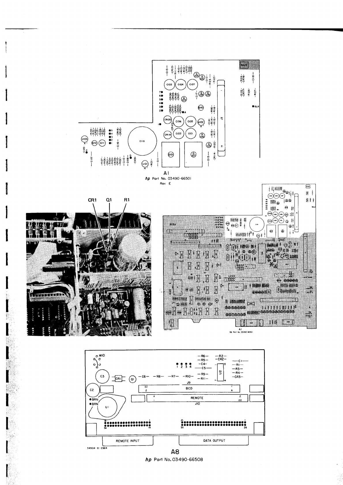
+l
*.- +ä
r r.t
Ä ll *iü
try | | +qr
ll
TTI"I
i:9
|
-
|
ETf
| |
AI I I
Tf
| |
,ll
/6\Rl I
\9trl
=l
|
+t
I
I
RlR a5 :!
TTf:: i?
/\a?l
lailrl ar 9
\_/ 6
I
xöln
IUr03l
v@
eal
I
!
I
hP Poll
A8
hp Port No.0349O-66508
I
'
I
1t,,
l.'
,.:,,,:
i':
:;' .,
r'
'';,,,:t',
l,'
l.:
l.
l
[.
ffi"
-nb- -Rz-
-R5- -CRz- _Ct_
aaaa -C4- -r--.ls _Rt_
| 2 3 4 _.Ä_ | I _-
| | -x5-
lE | -A4-
-c6- -R8- -nz- -nro- -f"- l- | -cR3-
REMoTE z
Jto
REMOTE
INPUT
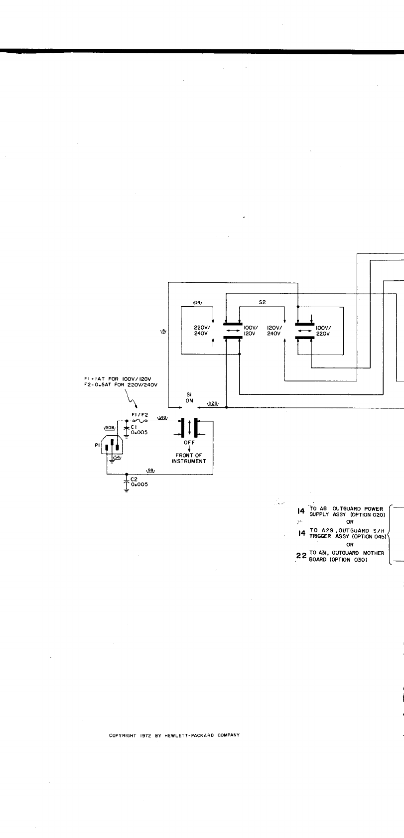
220V/
240V t20v/
240V - 3::,i
toov/
t20v
+3OV REGULATOR
-3OV REGULATOR
ON
i
FRONT
OF
INSTRUMENT
ta io ag curGuaRo powER
' ' SI,JPPLY ASSY (OPTION
O2O)
/oR
ü TO A29,OUTGUARD
S/H
rr TRIGGER assy (opnoil o45)
OR
22 Ig t31,.9_uIGgARo
rr,rorHER
I rWen
suppLy
BLocK DTAGRAM
-- 80ARD (OPT|ON
O30) | _
c|7
o.05
COPYRIGHT I972 8Y HEWLETT-PACXARO COMPANY
Figwe 7-26. Schematid
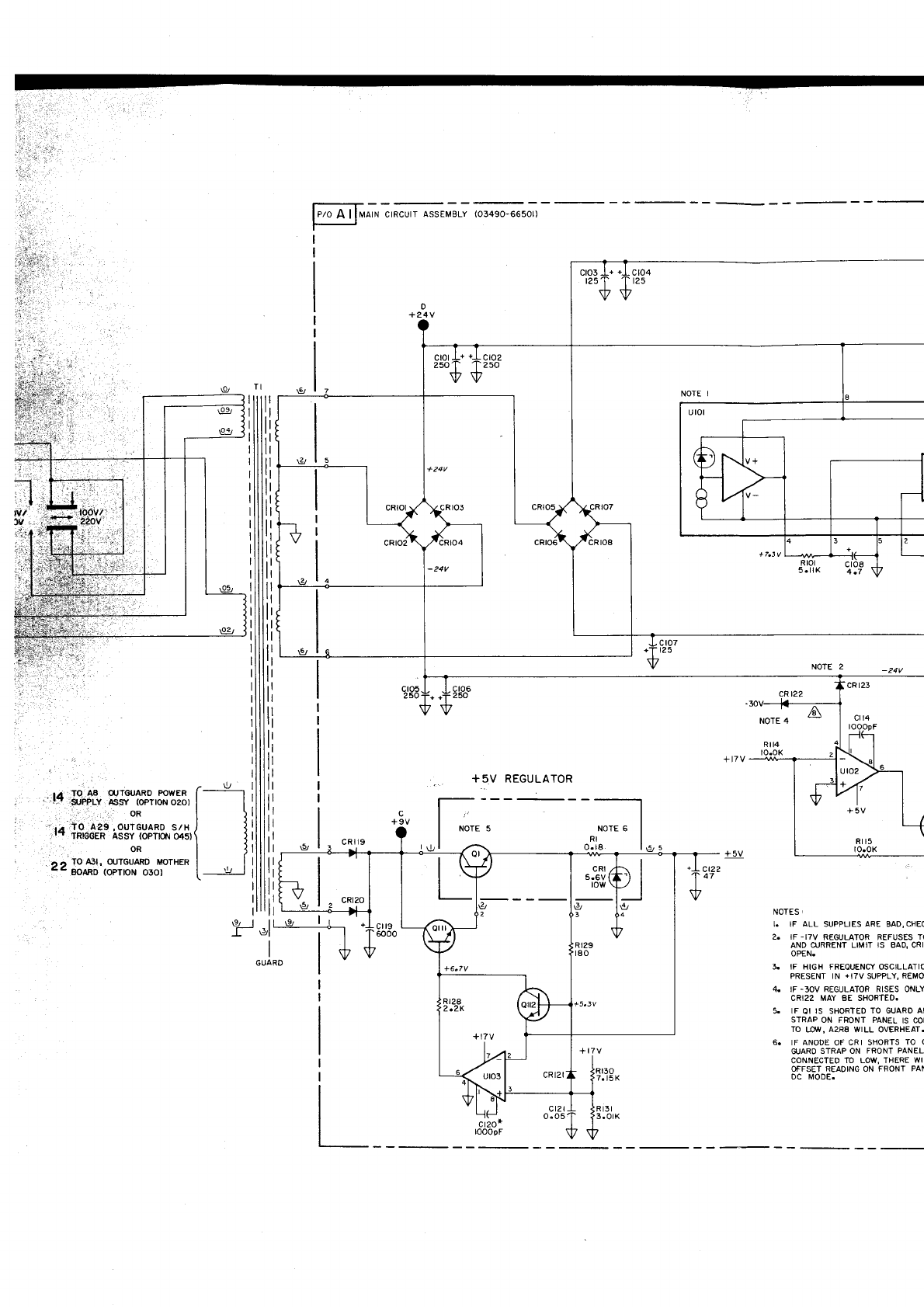
,l'
rr TO
Aa OUTGUARD Powen l'
rI grppry assr (optror'r
ozot I
' ..
..'..
', ,',..,
oR I
rr TO A29.OUTGUARO
S/H /
rr TRTGGER Assy {oPTtoNo45}\
oRl
,, To ßt, oUTGUARD MoTHER
i
-- goARo
(oPToN o30)
\9lll\9ll
J-*i
lI
ouiro | \Y
NOTES
.
I. IF ALL SUPPLIES
ARE BAD,CHEC
Z. IF -I7V REGULATOR REFUSES
T(
AND
CURRENT LIMIT IS BAO. CRI
OPEN.
IF HIGH FREOUENCY OSCILLATIO
PRESENT lN +l7V SUPPLY,
REMO
IF -3OV REGULATOR RISES ONLY
CRI22 MAY BE SHORTEO.
IF OI IS SHORTED
TO GUARO AI
STRAP ON FRONT PAN€L 15 COI
TO LOf, A2R8 WILL OVERHEAT.
IF ANODE OF CRI SHORTS
TO (
EJARO
STRAP ON FRONT PANEL
CONNECTED
TO LOW, THERE
WIl
OFFSET READING ON FRONT PAI
DC MOOE.
REGULATOR
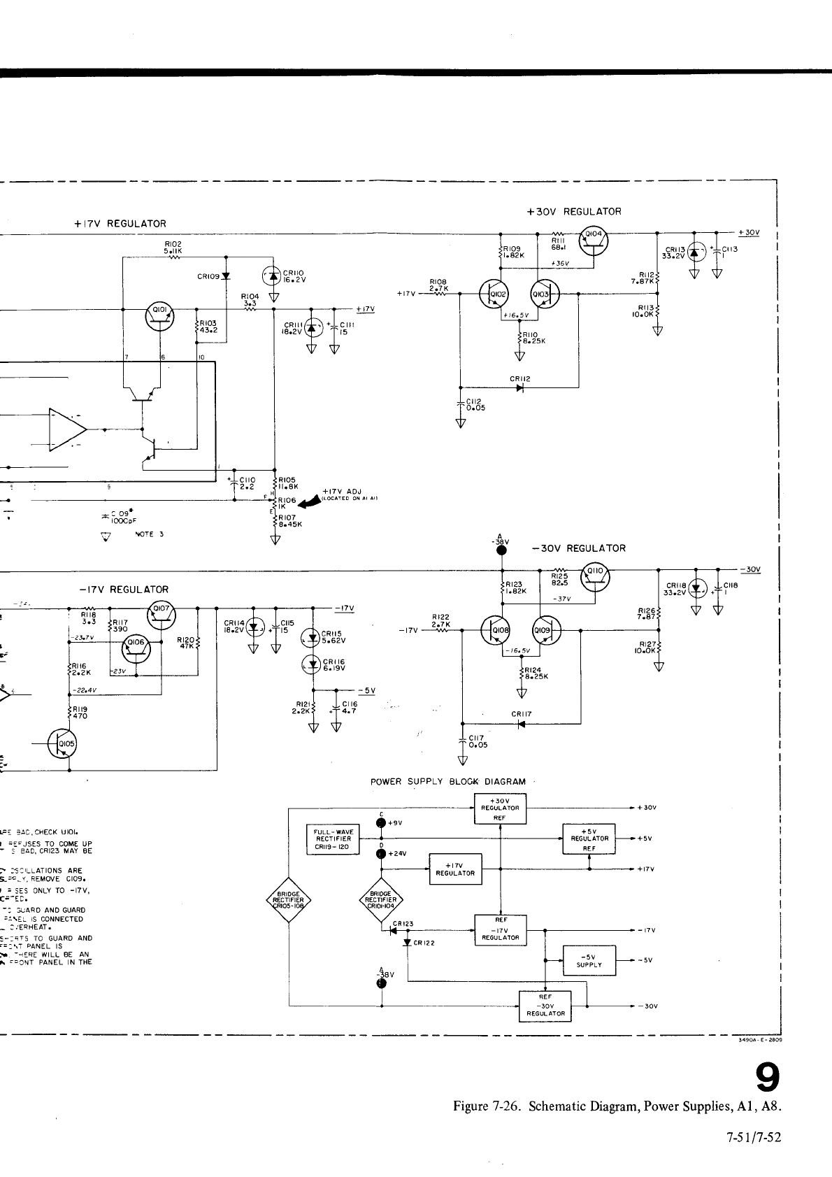
+3OV REGULATOR
+ l7v REGULATOR
Rr05
ll'aK +r7v aDJ
R 106
aj(tocarED ox
ar
all
R
r07
8.45
K
_3OV REGULATOR
-I7V REGULATOR
9
Schematic Diagram,
Power
Supplies,
Al, A8
7-5117-s2
Figure 7-26.

I
SCAN
A \9 J
FUNCTION
A €/ f,
FUNCTION
I €/ c
+5V ü C
SAMPLE RATE g 3
POLARITY
\5 c
RANGE B Ü C
RANGE
C Ü 3
RANGE A \? O
-n2-
- R4-
- R3-
|--*-l
8ta
I
C €g REMOTE
C €J' DATA A
C €9 DATA O
C
€C GROUNO
. ,s S/H l,lODE L
tüt(?^*J
C €} DATA B
C re2, SCAN C
o €, SCAN
B
OVERLOAO Ü O
A3
hp Port
No.
O349O-66503
REV. B
DS7
N6
DS6 N5
u55 N4
os4 N3 N2
DS2 NI
DSI
BCD to Decimal
Conversion
Table
Decimal
Number
0
1
2
3
4
5
6
7
8
o
BCD
DCBA
LLLL
LLLH
LLHL
LLHH
LHLL
LHLH
LHHL
LHHH
HLLL
HLLH
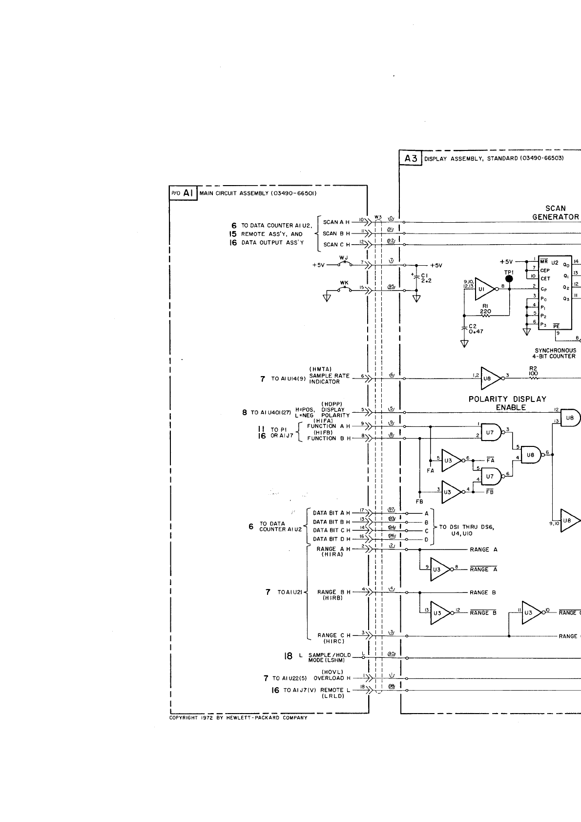
MA|N
CTRCUTT
ASSEMBLY
(
03490-6650r )
(
HMTA}
SAMPLE RATE
' I
U AI
UIA{V' INDICATOR
(
HDPP)
8 roaru4oreil
i=i33'
SfTH[r-+:
DISPLAY
ASSEMELY, STANDARD
(03490.66503)
POLARITY DISPLAY
ENABLE
MR UZ Oo
CEP
cET ot
cp Q2
P6 03
P1
P2
P: Fe
COPYRIGHT I972 8Y HEWLE1T-PACKARO COMPANY
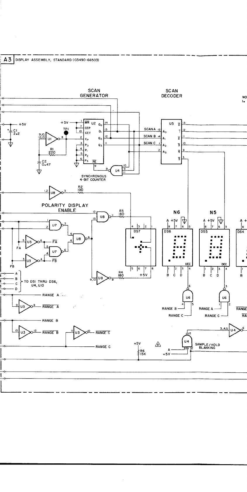
; A3 lorseuv assEMBLy,
sTaNDARD
(os49o.66503)
SCAN
GENERATOR SCAN
DECODER
scalrör f-* I
FUNCTIONA€rf | -- I
FUNCTIONB\cc Ü
+5V
üc
?cv v J
SaMPLE RATE 'r o f---'-;;--l
POLARITY\9c I I
RANGESsJ ;--------_.i;
RANGEC\t/J 7
RANGE A üJ r-----:::----.1
oVERLoAD
Vc | ,, I
c2
o.47
SYNCHRONOUS
4.BIT COUNTER
R2
roo
POLARITY
DISPLAY
ENABLE
FB
It
r-A I
+Rl
| ^ : Fro DSt rHRu
os6,
Tl-: I u4, uro
T..,-"J RANGE A
RANGEI RAiIGE
FII
+5V ASAMPLE
/ HOLD
SLANKING
t5K
frE UZ oo
CEP
cET 01
cp Q2
Ps 03
P1
P?
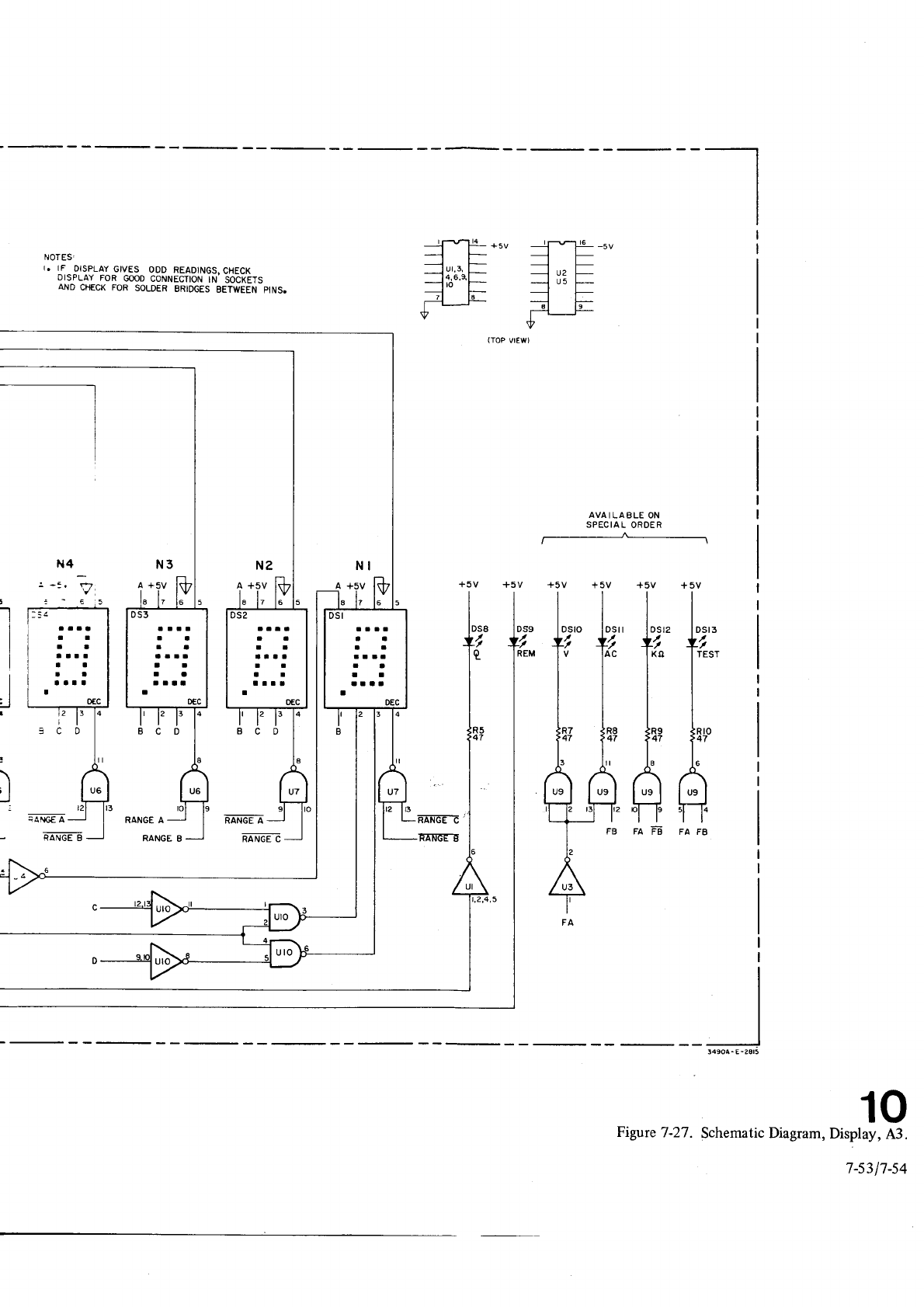
NOTES.
t. rF-otsplAy ctvEs oDD READTNGS,CHECK
DISPLAY
FOR GOOD
CONNECTION
IN'SOCKETS
AND
CHECK
FOR SOLDER
BRIDGES
EETWEEN
PINS.
____{vl]l_+sv __r1r-q'l_L
-lr---
---1"' r l--
4:1-:l- - !2 +
---{io"*F -i.. F
=E=E
Bl ls
vv
(TOP
VIEW)
AVAILABLE
ON
SPECIAL
ORDER
+5V
+5V 1".,,1,,,.
Y, +,
l-"1""
tt
l*' l"
öö
"l
r1l"
ra FE FA FB
aaal
aa
lt
lttt
al
It
lall
ataa
al
aa
aaal
ll
aa
atll
10
Figwe 7-27. Schematic Diagram,
Display,
A3.
7-s3l7-s4
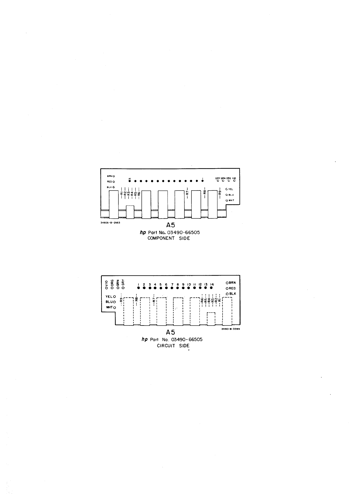
ta | 6FY GRr OFG
Vp
a a a a a a a a a a
a a a
a oo o o
++++++
A5
hp Port No.
0349o-66505
COMPONENT
SIDE
A5
hp Port No. 0349O-66505
CIRCUIT SIDE
OBRN
OREO
.O 8LK
I
I
I
I
i
r'!!
++++
i
|
| I
rl
i'---1 |
iii
t2t456?89rOil121314
aaaaaaaoaoaooa
-aö ---. i--a
tT: iT! i
|
|
| |
r;
rlril
ir:li
itiii
rll
I
=E
uo
oo
ti\.-
cl
I
^9
YG
>o
oo
YELO
BLUO
rrHTo
!---tö;
; iTT
rl
rl
ll
ii
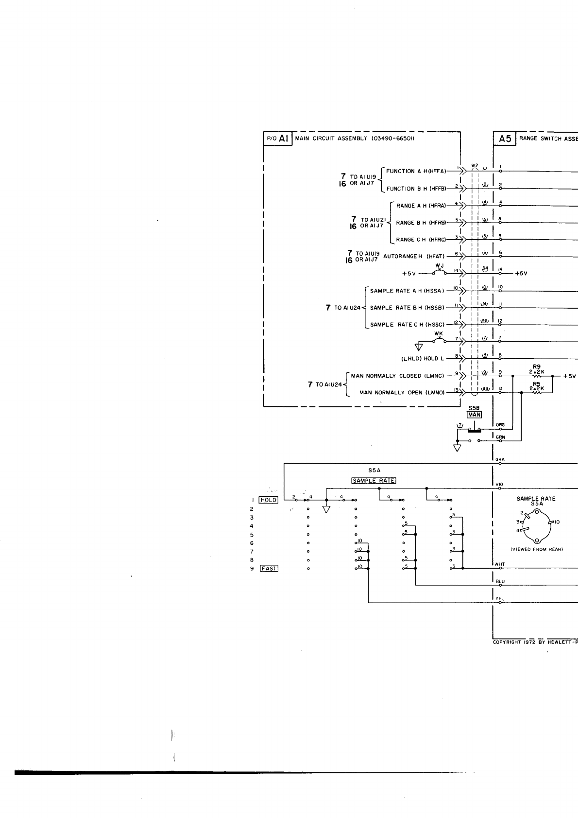
MA|N
CTRCUTT
ASSEMELY
(03490-6650t)
*"-r.t tE-oro-u*oi ffiJ-*orie-r*E oG
tt-
[-rurucrroru
a H(HFFA)
'i\-X-!-l ]--
.Zrslrqr'l i'ii l
16
oRAr ,t l_rur.r,o*rr,rro,_$;11*|3
t-nqNae^r,*.,'i, I l*
l,
,E
;:ll:;'l RANGE I
H'**'iL
[-.o*0..",r*.,j#
'ä;glYr
^".^.r"
l-saucr-e
RArE a H
tHssar
---$P
7 roo,u.o]
saMpLE
RATEBH
(HssB)
i I l* | -
l-ro"r..
RArE
c H
,rrr., ''t''fl*l*
{-#'-d.ir'l J
,.*.ol"o.o.
.i
I
i'!
r -,
R9
l-r*atl
Honuallv cuoseo
tr-r'rr'rct
--)}f
7roatu241 | ll
l- r,raH
NoRMALLY oeer.r
tuuHot--)-!l
+5V
i i.-l
,.
(LMNO)
Is5B I
IMANI
I
r7t | | o*c
i |.qdFl
2
6
7
g l?adil
SAMPLE
RATE
S5A
:Lhl.r\"
: qil "-.1
i"<)
or!-l.l l-\9
*-1 . | "f I tvreweo
FR.M REAR)
*1 fJ
-l I r,,,
I
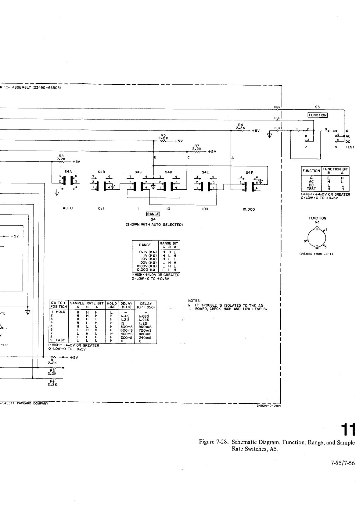
r -:r ASSEMBLY
(O349O-66505)
,l lFUNcroNl
l-
fl
FUNCTION
;UNCTION
BIT
8A
AC
0c
TEST
LH
HL
LL
HH
lFaN6E-l
s4
(SHOWN
WITH AUTO
SELECTEO)
I
=HIGH.
+4.OV OR GREATER
O=LOw.O
TO
+O.5V
Ft tcTtoN
s3
/A
/-\'
fl
o4 I
-\1,
(VIEWEO
FROM
LEFT)
11
Function,
Range,
and
Sample
RANGE RANGE
BII
CBA
o.r
v
(Ko)
.
tv
(Ko)
rov
(Ko)
roov
(Ko)
rooov
(Ko)
r0.000
Kn
HHL
HLH
HLL
LHH
LHL
LLH
l=HIGH=
+4.OV
OR GREATER
o=Low
=o
To +o.5v
NOTES.
I. I F TROUELE
IS ISOLATED
TO THE 45
. BOARD.
CHECK HIGH AND LOW LEVELS.
r.r - err -
plc-xlno aOM
pÄNt- 34904-
D-28t4
Figure
7-28. Schematic
Diagram,
Rate
Switches.
A5.
SAMPLE
RATE BIT
CBA DELAY
(STD)
I HOLD
6
7
I
9 FAST
HHH
HHH
HHL
HLH
HLL
LHH
LHL
LLH
LLL
i
H
d
H
H
H
H
H
'. os
t.2 s
ts
SOOhS
6OOmS
40OmS
2OOhS
o
O.LOW=O
TO
+O.5V
R6
2.2K
7-ss
17
-s6
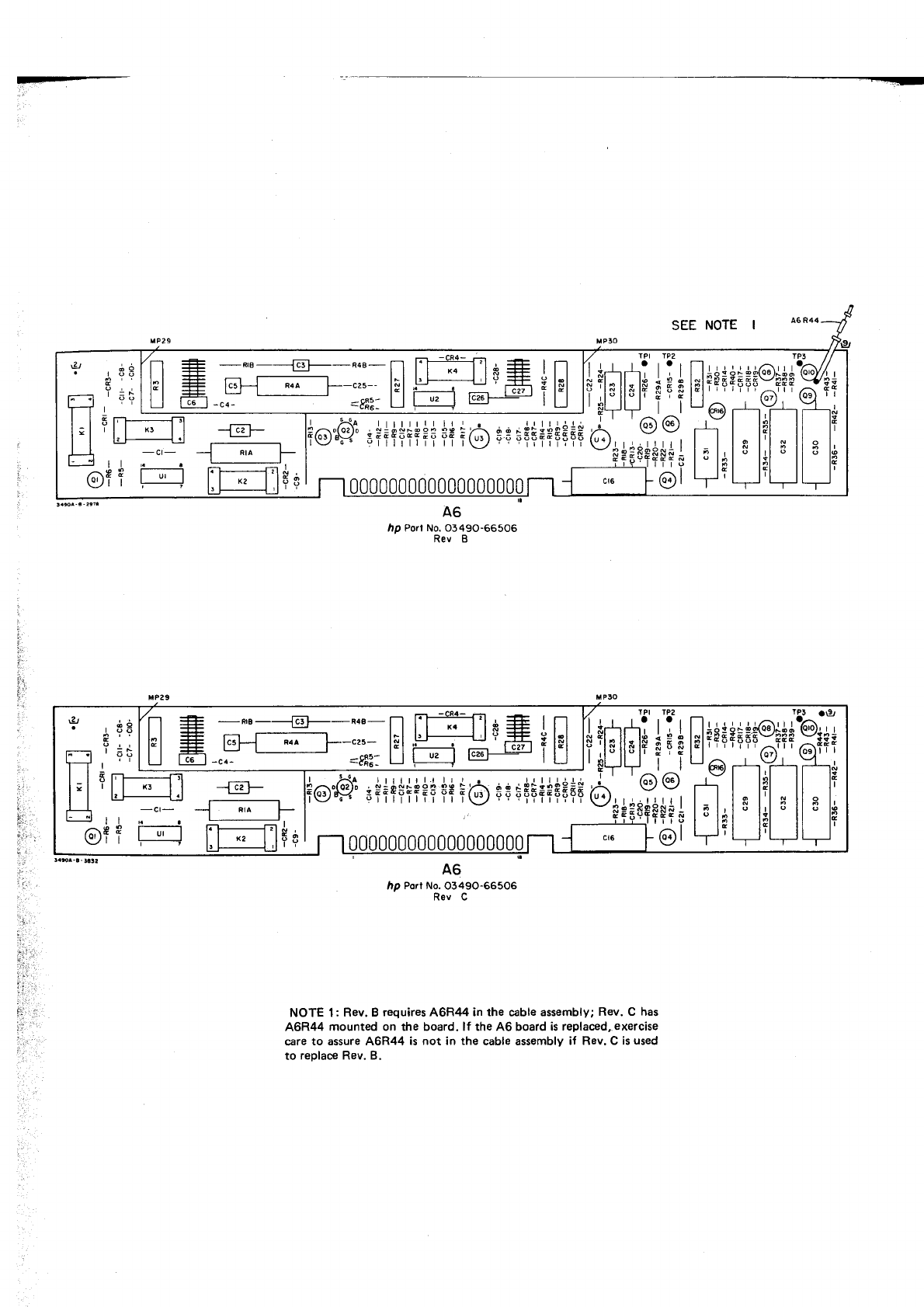
I
I
I
I
I
Y3
g
(os)
|
Y
t-t
tl
t3l
t"l
+
$ütE@ü$$
rtt' l
ll
toTl
M
l-_l;l-l
|
-
lfl
-
|
f+f
/ rPt 1P2
'|
rrtororf-l ,,,
+iElEl+
ftf$l$lr?q
il++ | lu6D
,\ @@ -'.."
***re4***l
l,lu
;l6t +'
e:tll
:
, ,
I lal a
=F | | |
??lll
f
FHI
tt KJ
tl
-ct-
l'..
B|---
l*
eJ
t"l
T-T I
llc
l-ll
tl
^9
Qj,J
- a__=!83-r
tl '*' '' -J Y:ff' ! lRl
lpl +F tjfi R41_l---c25-- lul ,F__- ,- rc?z
I i t'l
U t-t -.; =sÄl-
[--l
t-i-] @-: | [J
A6
,rp Pofl No. 03490-66506
Rev B
./ rpt rPa
| | | r o r o r l--'1,
rilitFt+
n*nlul+++
'E++ | 1"6")
Ä' @@ .'-.'-
"+*ge****l
l,lr
-;;l@l +T
@"9.'
*+++++++++++@
$$ F+F+++F+F
-@-
--1 Rra f-
l.-21-,
l.l K2
I lTq
eJ ':Yl-\ :
' r SEll
| :
.------ ti*ll"l :
t' 't ?Yt | | r
T_T I
llöl'-!l
l;l rl
I xr I I
tt k_-i
tl -ct-
l-.1 ll[a
rilf ? I-;-l
\--z | | i-_-----t
n +E -R,B-----lTtl--R4a-n l-t-=""+t, + | r--l
l'l # 6-r;=-1--:.'- hl
.u
..Jl$#;lul
ll tffl-.; =8Et-
l-l l-sJ I-I-: I U
,tp Porf No.
03490-66506
Rev C
NOTE 1: Rev. B
requires
A6R44
in the cable
assembly;
Rev. C has
AOR44
mounted on the board. lf the 46 board
is replaced,
exercise
care
to assure A6R44 is not in the cable assembly
if Rev. C is
used
to replace Rev. B.
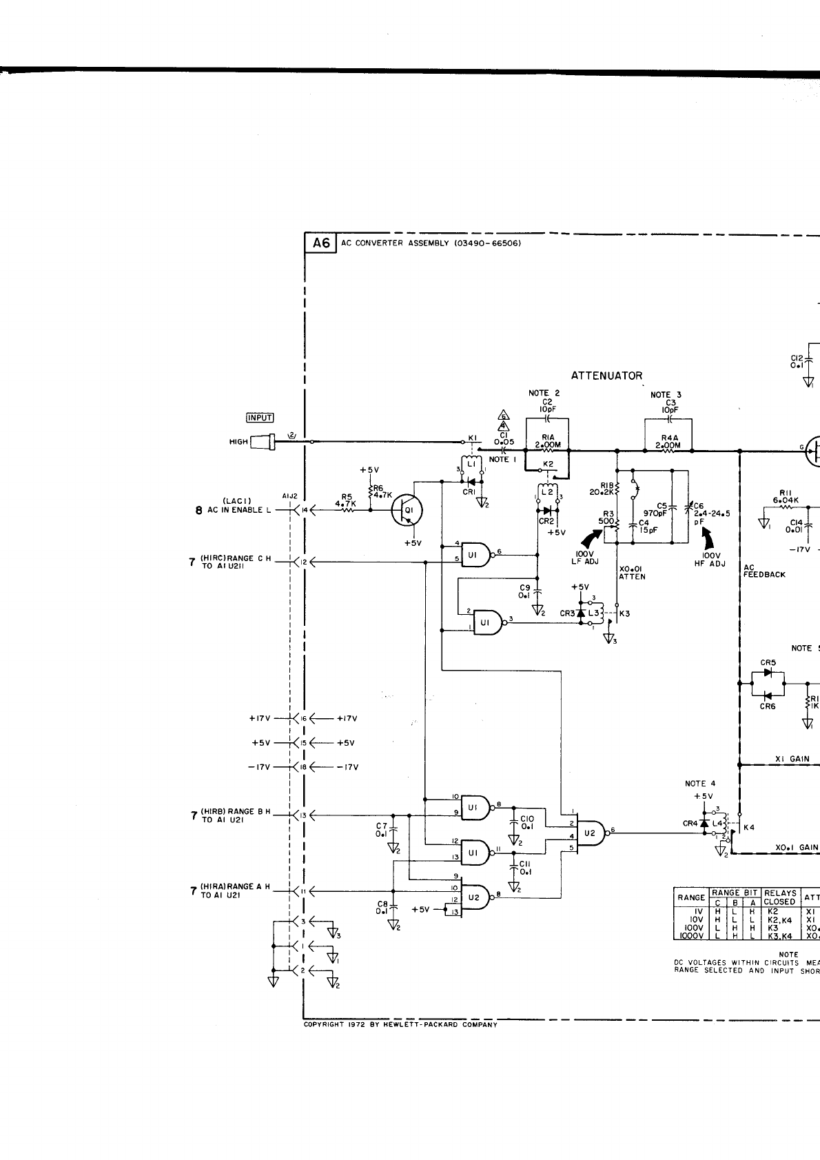
[A6T* .*""; ;r*.*' *;-..u*,
t-
I
",, -[-
,T
ATTENUATOR
xo.ol
TEN
NOTE 3
lOpF
(LAC
I
) AIJz
I Ac lN ENABLE t- ---|(h
?(HIRCIRANGECX 1,,
' TO At U2il | \'-
(
toov
F ADJ
2.4-24.5
pF
I
toov
HF ADJ
NOTE 4
+5V
NOTE
OC VOLIAG€S
WITHIN CIRCUITS MEA
RANGE
SELECTEO ANO INPUT
SHOR
Rtl
6.O4K
r*_T_
V, ^cK+
"'"1
-t7v -
? (H|RB)
RANGE
B
H
___j:1
,z
' TO Al U2l |
\':
I
'(HIRA)RANGEAH I
tntharnANuEAn i/..
TO
At Uzt i
\'-
+tzv
---f(re (- +rzv
rl
+5v
--+<r5
(- +5v
-,,u-1,16--,,u
e---r
V.
<---l
v
<---r
V.
llNPUil
HIGH
COPYRIGHT
1972 8Y BEWLETT.PACKARO
COMPANY
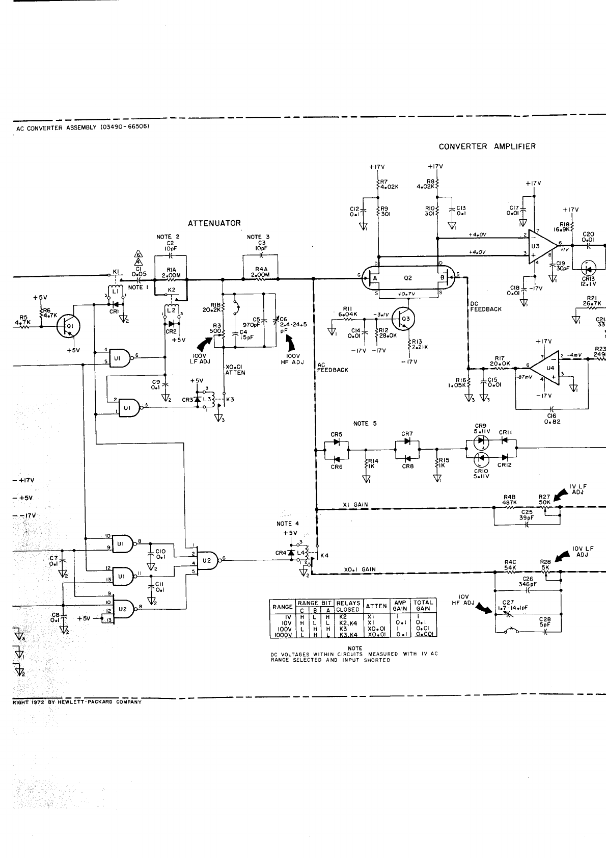
AC CONVERTER
ASSEMELY
(O349O-66505)
CONVERTER
AMPLIFIER
+
r7v
R8
4.OzK
Rlo
301
t2.tv
Rzl
26.7K
I
\/ czr.
'' 33'
I
Rrl
5.O4K
DC
FEEOBACK
+r7v
R17
20.
oK
- t7v
IV LF
ct3
7
.ozK
R9
301
ATTENUATOR
- +l?v
- +5V
111.i?V
K? ct8
^r
o.o|
i
V
+5V
ct4
o.ol
-t7v -t7v Rr3
2.?tK
toov
LF ADJ
+5V
xo.ol
ATTEN FEEOBACK
3
ct6
o.a2
cR9
5.llV CRtl
cRro
5.r
rv
1l oot
X I 6AIN
XO.I GAIN
HFADJT ^
ti
v
?,
NOTE
DC VOLTAGES
WITHIN CIRCUITS
MEASUR€O
WITH IV AC
RANGE
SELECTED ANO INPUT
SHORTED
RANGE RANGEBII RELAYS
CLOSEDATTEN AMP
GAIN TOTAL
GAIN
c
tov
toov
n
I
L
L
n
H
L
HK2,K4
K3
XI
xl
xo. ol o.l I
o. I
o. ol
RIGST 1972 BY HEVTLETT.PACTARO
COMPANY
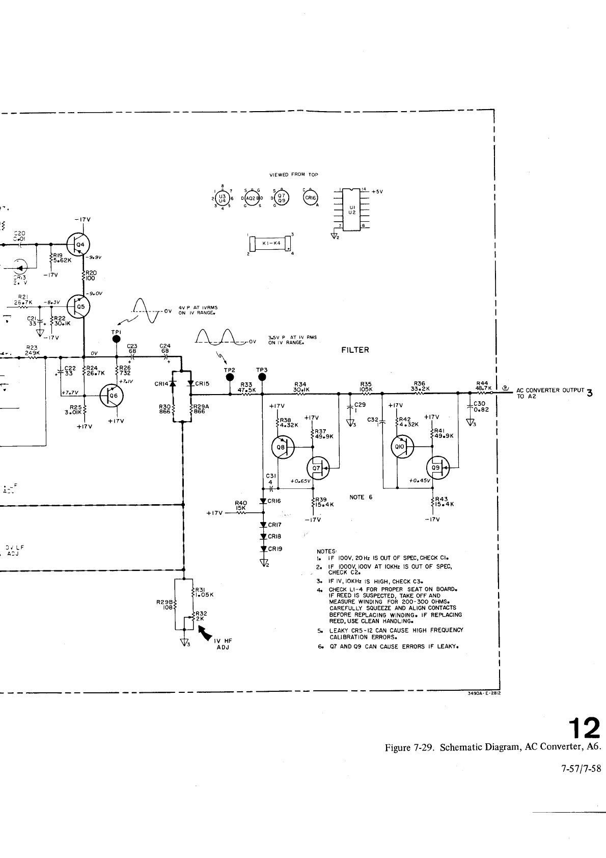
vtEwEo FROM
ToP
'.@J'"@i":@
@^
3Rr3
l. v
R2
?6.7K
c2l
55
C/ LF
'r---\-
-7-
ov
,---t V
TPI
ON IV RANGL
-8.3V
ov 3.5V P AT IV RMS
ON lv RANGET
c23
68 FILTER
NOTE 6 R43
t5.4 K
NOTES'
l. lF loOV,2OHr lS
oUT
OF SPEC,CHECK
Cl.
2. lF IOoOV
loov AT IOKH! lS oUT
OF SPEo,
CHECK C2.
3. lF lV, IOKHZ
lS H|GH, CttECK C3.
4. CHECK LI.4 FOR
PROPER SEAT ON BOARD.
IF REED IS SUSPECTED.
TAKE
OFF
AND
MEASURE
WINDING
FOR 2OO.3OO
OHMS.
CAREFULLY SOUEEZE
AND ALIGN CONTACTS
BEFORE
REPLACING
WINOING.
IF REPLACING
REED.
USE CLEAN HANOLING.
5. LEAKY
CR5-12 CAN CAUSE
HIGH FREOUENC/
CALIBRATION ERRORS.
6. 07 AND
09 CAN CAUSE ERRORS
IF LEAKY.
R44
4t].7 K 9l nc corvepreR ourPUT
1
TO A2 V
R25
3.OlK o.82
+ t7v
+r7v
t
12
Figwe
7-29. Schematic
Diagram,
AC Converter,
A6.
1-s7l7-s8
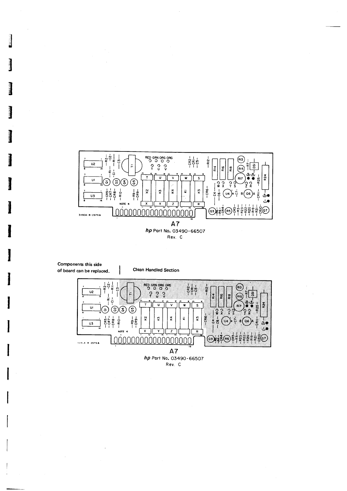
f, ^au
l-O999-06t90
'oN
lrod ofq
LV
uoll3as palpueH
uea|c
3 ^au
20999-O6t9O
'oN
uod drl
LV
'paceldat eq uq) pJeoq
lo
epls s!ql sluauoduioc
@*++++++iei+ot
oT, 'l
=,?"@.+"@+i,*
I L Ez s^ x/v\l
I li, Oo,/-\ao cQl
l*lT;a9nrn
LJ
riu@ lällall*l
' 'i-i6 L_lULJi
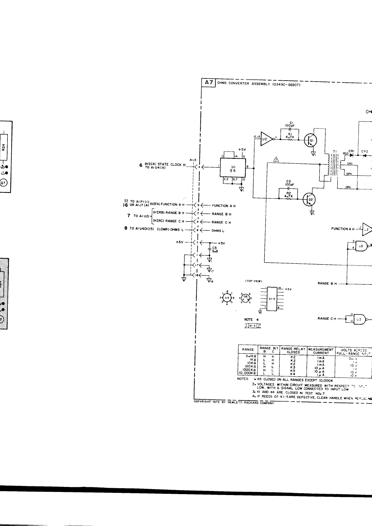
i --c 3!
_ ^rvdo3 ouvlSvd -ulil3j
N3H,$
3-ror{vH
NV:nC'3Au93J3C fuvs_tr lo so3fu Jl.,
L.oN lstr Nt
o3so_]c 3UV 'x oNv tx .e
. _ ,1O_l
_IndNt
OI offCfNNO3 AO-t 1VN9|S
ü Hl.l^t ,f\O-]
:r :- rtfds3u H.!,r\ o3ansvln r|n38t3'täiili ölövriön .z
,ooo'ot 1d33X3
SI9NVU
-l-lv
No
ofso-]3
9X.l s310N
---
-{."1 r_H339NVU
\_ra -
:tr'-Ei
-rF.4
---l L- s^t
=''^F ""Q4"
"
no*J F
mJ.
.\y',
H 8 3ONVU (ffll^ dof )
H V NOITONNJ rsnxo
-) it -t
snHo(unor)
(gt)tornrv
or
tl
lr
e 3eNvu
-J r).|-- ", ,oro, ,arart
t'. I
H
v Norr.cNn.r
+ i l_ , v
norlrr,rn:
{v:rx)
[li,i.,,J
Bl flt
)- *co",c
'ifl3?;5fö
ertv ls
E
[rO
v/ol
v'ol
vu I
vu I
vul
u>1
€t
€t
Z>1
zr
zv
1-l
'lH
'lH
H'l
H-i
HH
uyooo'ol
o y
oool
nxool
olol
üyl
ült.o
3S:.:v S1-lO^ 1Nf8Un3
rNSnfunsv3lrl o3so't3
^v't3a
39NVU
u8 f9NVA 39NVU
lo
001
(
10999
-06t90) l.18n3SSv
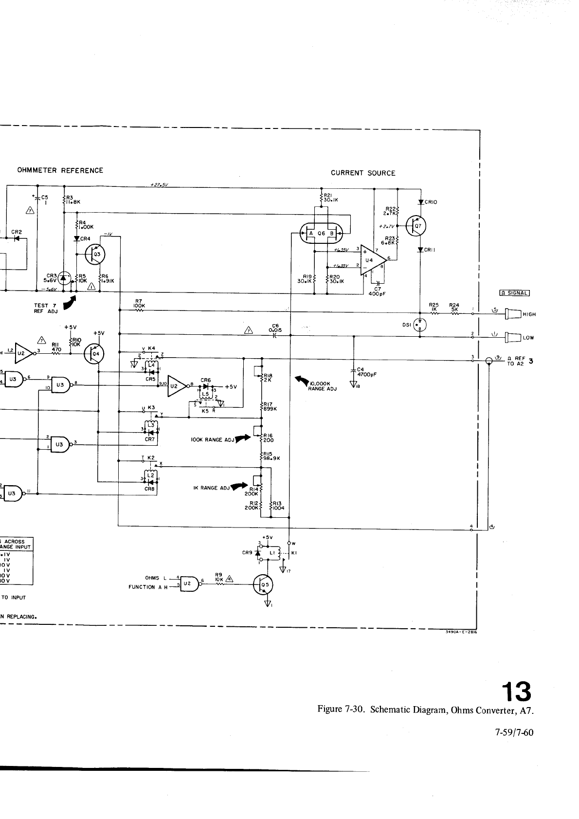
0vLl6s-L
'rV 'relJo^uoJ
surq6
'urur8erq
crlerueqcs
.gE-1
arn8rg
8t
.9Ntw'1d3u Nl
lndNt ot
l- ^o
I AOI
| ^l
J ^ol
I ^l
l-------11:
lmdNt 39Nv
I ssoucv I
),,*
33N3U3J3U U3t3NltHO
l3unos
l'N3UUnC
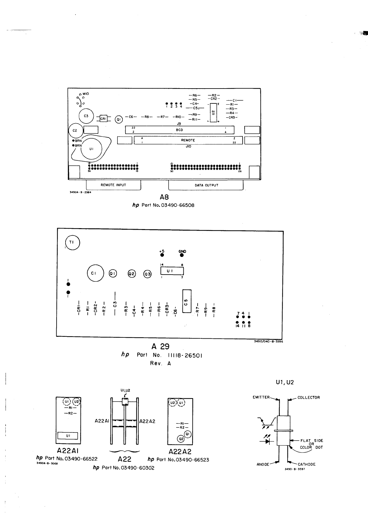
l;U
r--r
GNO
a
14 g
l-u'
-l
l7
@o @
@
I
I
s
lrliJü
ITTTTT?9
I
a
o
I
I t.l
I
E=E,N
?;?T
tll
Fo@
f f I tc r
| |
| aoa
aao
t4
lt I
hp Port
No.
o349o-66522
3490A-A-
5002
hp porf 429
No. llllS-26501
Rev.
A
422A2
422 hp pott
No.03490-66523
Ul,U2
A22Al
A22Al 42242
hp Port
No.0349O-60302
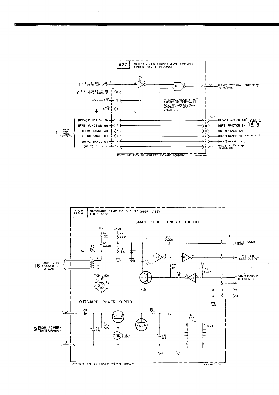
1M1 3äY'ä'^i äT? "lTl'-?'.1.'.i"
aSSEMBLY
rB
üffis'8"{-l-]l
TO A28 \--
, tF?tr
J.luE[{
.sv--<+{lk,l < rsv
TRIGGER ASSY.
SAMPLE
/ HOLD
TRIGGER
C IRCUIT
Jtl
I
#'frcPJfrGcER
, STRETCHED
- PULSE OUTPUT
Z'"'+.gntl,"*LS-*
!
(LEXE)4EITERNAL
ENCOoE
7
? SAMPLE/HOLD
' TRIGGER L
ll
OUTGUARD SAMPLE/HOLO
(il il8-6650t)
+5Vl
R6
2?K
OUTGUARD POWER
SUPPLY
5Vl
I
I looo
1.o
To.oor R5
t2K
4+5V I
I
I
.l
3390
iIAND
rl
tF SaMPLE/HoLD
rs Nor I
TRIGGERING
EXTERNALLY I
AND THE SAMPLE/HOLD t
^<sMar v lQ nMn I
! I AND THE SAMPLE/HOLD t
r--{*g+<l<--.r fff.ItTrs
Gooo' i
v it v I
i I lauz
,rrou
rn-p-(] Ä)-i-urrat FuNcnoN
an\7r8JO,
rroN
eH
i<, < > ä
y5rxrrat FUNcroN er
J 13, 15
[txttotFuNcroN
*i<] i#-1u1ra1
FuNcrroN
aHl48i!C
|trrrretFUNcT|oN''{i9}1-.n''',FUNcT|oNerJl3'|5
iffü' J (HFRA)RANGE
or-Xi l;j-rrc*or nmoe nxl
'.,i.it.".'.)(HFRB)RANGE''--t<il>-.i-t'.*'rRANGEBH}roa'uzr/
I tr.*.r RANGE
cH
-i<l l;1-rt".ct ^otn.
.r J
l- rxrnrr
^"" '*i l+l8o^yJl,flylo
t 7
COPYRIGHI 1973 BY IEWLETT-PACKARD COiIPANY !4e-a-35s6
TI
TOP VIEW
.rd. ,
7,,n',\.
+gV/o
R2
COPYRIGBT 1973 8Y HEWLETT.PACKARD MMPANY 3490r'040-C
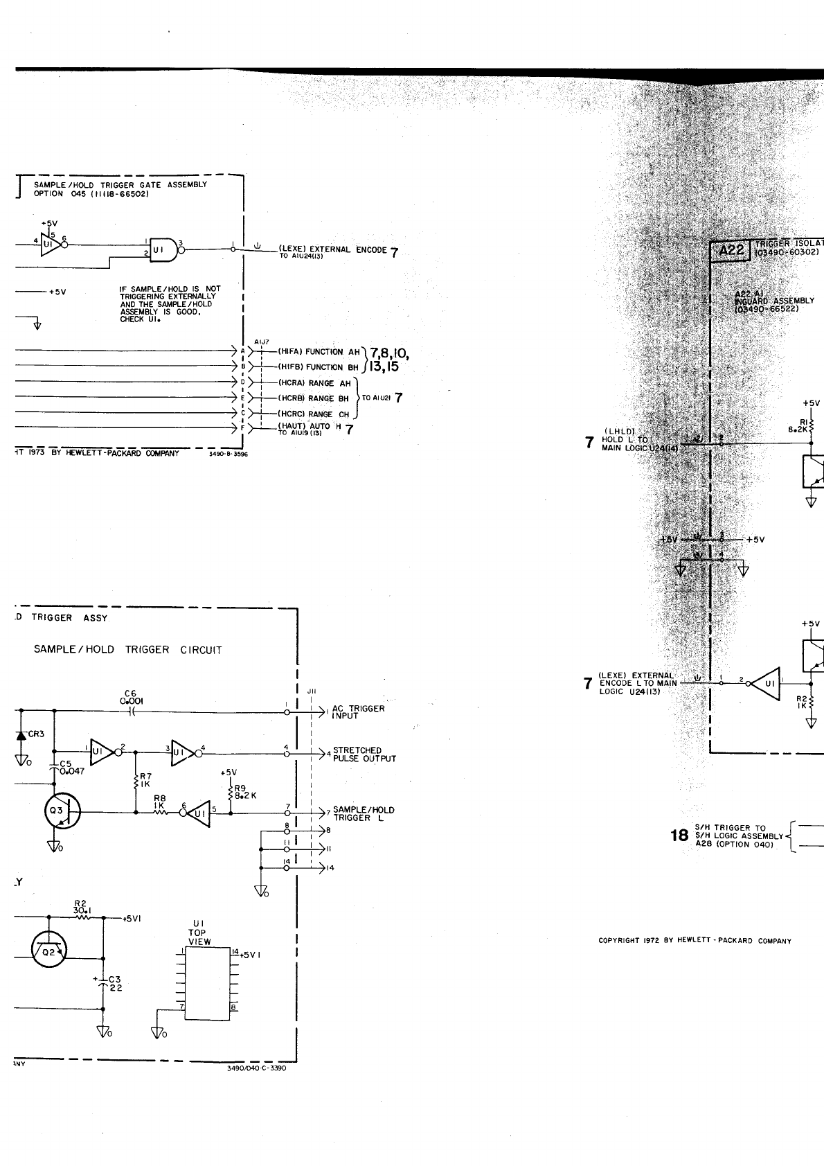
,;;,..*
'.,
SAMPLE/HOLD
TRIGGER GATE ASSEMBLY
oPTroN O45 fiilt8-665021 II
,ij;
.;;i
t;;:'l,:,;t;;1
.::..:.1!;i;:l
-":;
:
..:!
;.1',
.D TRIGGER ASSY.
SAMPLE
/ HOLD TRIGGER
C IRCUIT
(LEXE)4EXTERNAL
ENCOOE
7
?
SAMPLE/I{OLD
' TRIGGER
L
(
LHLD) '
HOLD L:
MAIN
(LEXE)
EXTERNAL.
ENCOOE
LTO
MAIN
LOGIC
U24il3) ,;
''il
'. ';,1
',r:l
r,: I
I
-^ s/H TRTGGER
TO
lö s/H LOGTC
ASSEMBLY<
- - 428 (OpTtON
O40) | -
\
-Y
E+SV I
,.rl
'l
"l
3490/O40'C
COPYRIGHT 1972
gY HEWL€TT.PACXARD
COMPANY
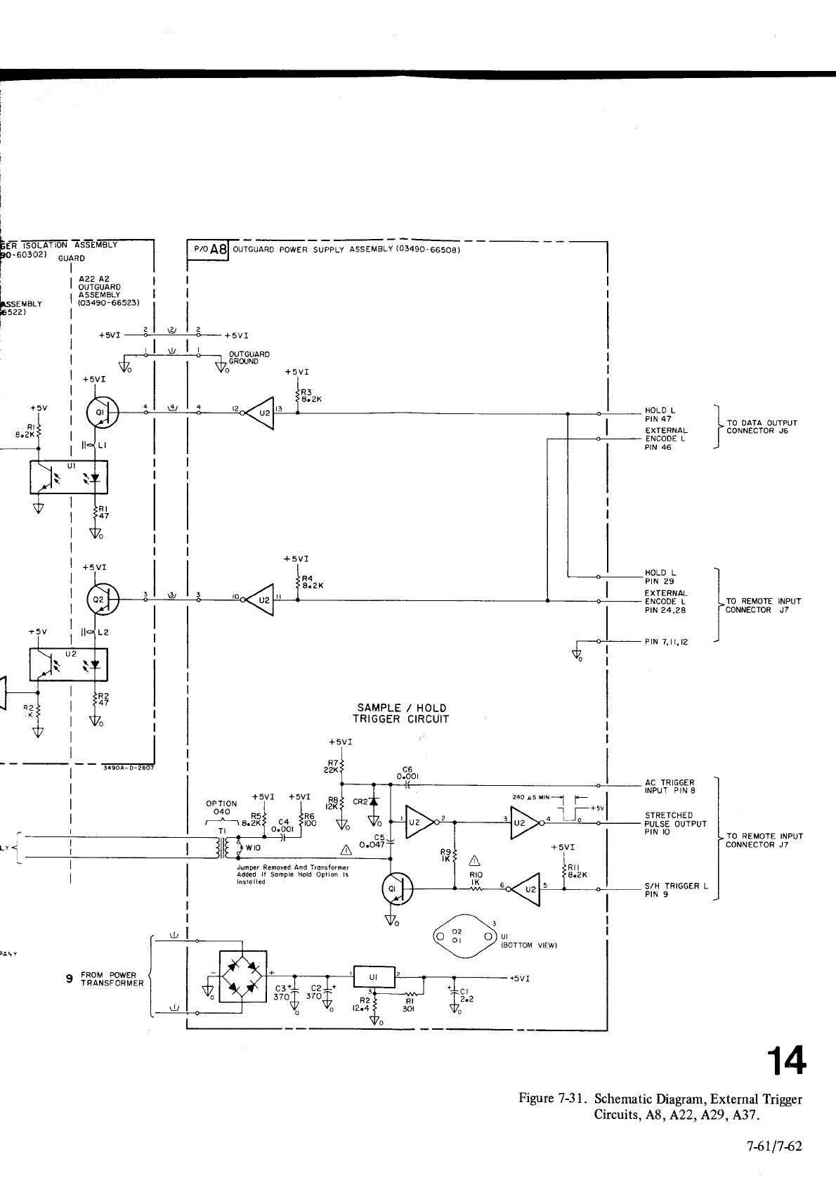
tl
--+f-!-l-tr- ourcuaRo
ü" | | üoGRouND
HOLO
L
PIN 47
EXTERNAL
ENCODE
L
PIN 46
HOLD
L
PIN 29
EXTERNAL
ENCOOE L
I ro ooro orrr'
J coNNEcroR J6
|ro *."or. ,*r*
-,J
coNNEcroR
J7
l":""'"
r____+ PtN
7.il.t2
ü"!
+5V1 +svr
AC TRIGGER
INPUT PIN
8
STRETCHE
D
PULSE OUTPUT
PIN IO
S/H TRIGGER
L
PIN 9
22K
R8
I?K
OPTION
o40
TI
,-'i
c4
o.ool
wro a
Jumper Removed And Tronsformer
Added lf Sample Hold Oplion ls
Inslo I led
TO REMOTE INPUT
CONNECTOR J7
A
Rto
IK
o FROM
POWER
- TRANSFORIVIER
14
Figure
7-31. Schematic
Dagram, External Trigger
Circuits,
A8, A22, A29,
A37.
SAMPLE
/ HOLD
TRIGGER
CIRCUIT
7411142
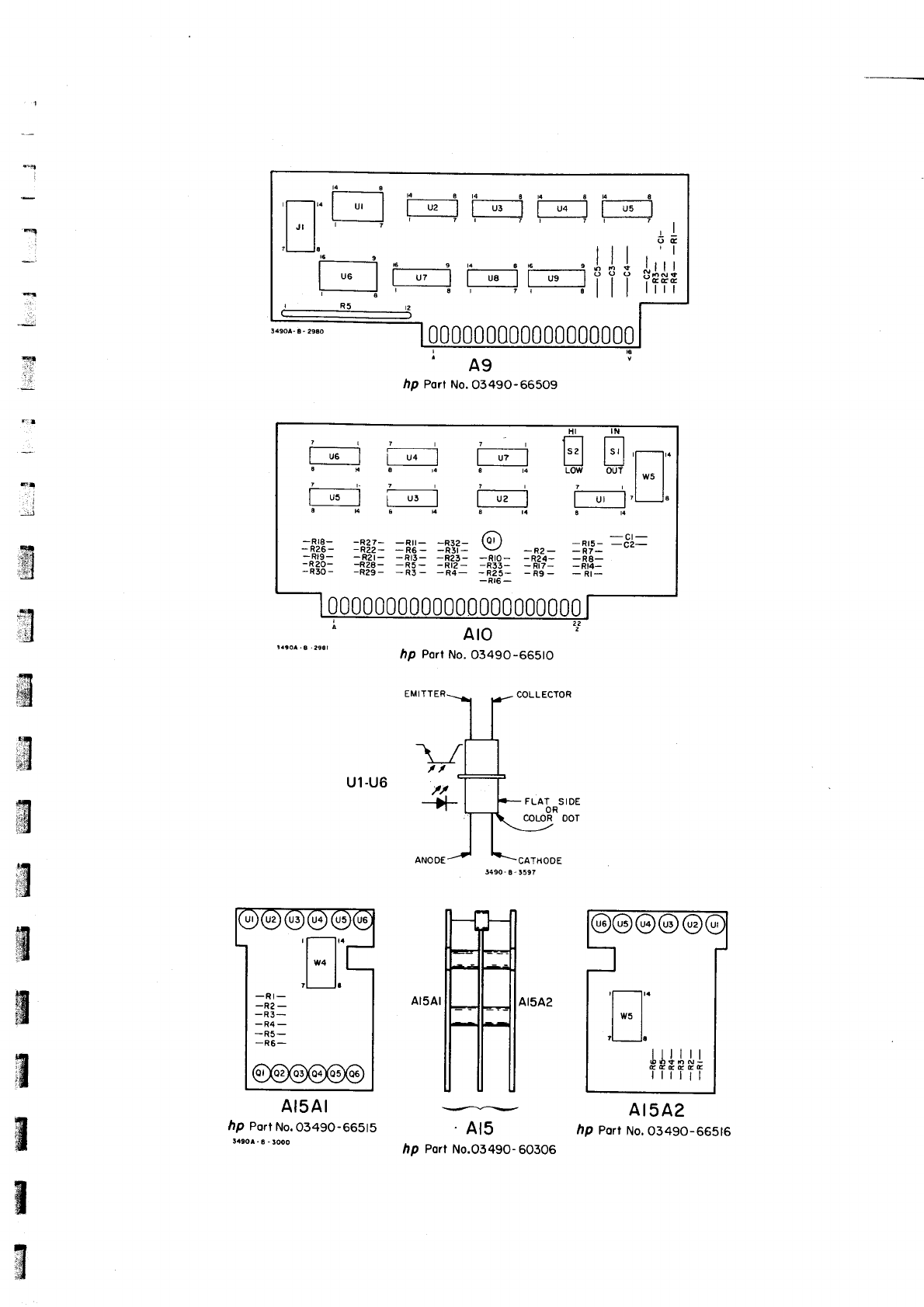
I
=
;,
F
iri
aa
T.
.;
:..i
?
5
,::,1
ä
,'g
#
,ä
ig
ä
'g
a
ä
g
3l
g
AI5AI
hp eort
No.0349o-665t5
la90l. a - looo
'A9
hp Pott
No.
o349o-66509
hp Port
No. O349O-665tO
-.At5
hp Port
No.O349O-
60306
AI5A2
hp Pott
No.0349o-665t6
EE
l'"1' f
'l l.
69
| ,r I [u;---l
t-tt-'l
l-----T
rrEir *J
lll,'l
!-------r ;i j Älll
I ur
ll ue l?i, ;eEc
:--------? r-----------" I I | | | | |
000000000000000
+
lu6llu4lluzl
8r€r.8t4
I ,u | t_ ,,3
-l l-ur-l
aß6t6ta
/::\ - cr
-
--Elq- -R27- -Ril- -R3z- (4r., -als- -iZ-
-826- -RZZ- -R6- -R3i- v -R2- -Rt-
--F!9- -R2r- -Rt3- -Rz3- -Rto- -RzA- _R8_
-829- -R2B- -R5- -Rt2- -R33- -Rr-t- -nü-
-R3o- -Rzg- -RJ- -R4- -R25- -h9- _Hi_
'l---lr.
tl
l*. 1
,ll.
TJlJJl
C€EEEE
tttttl
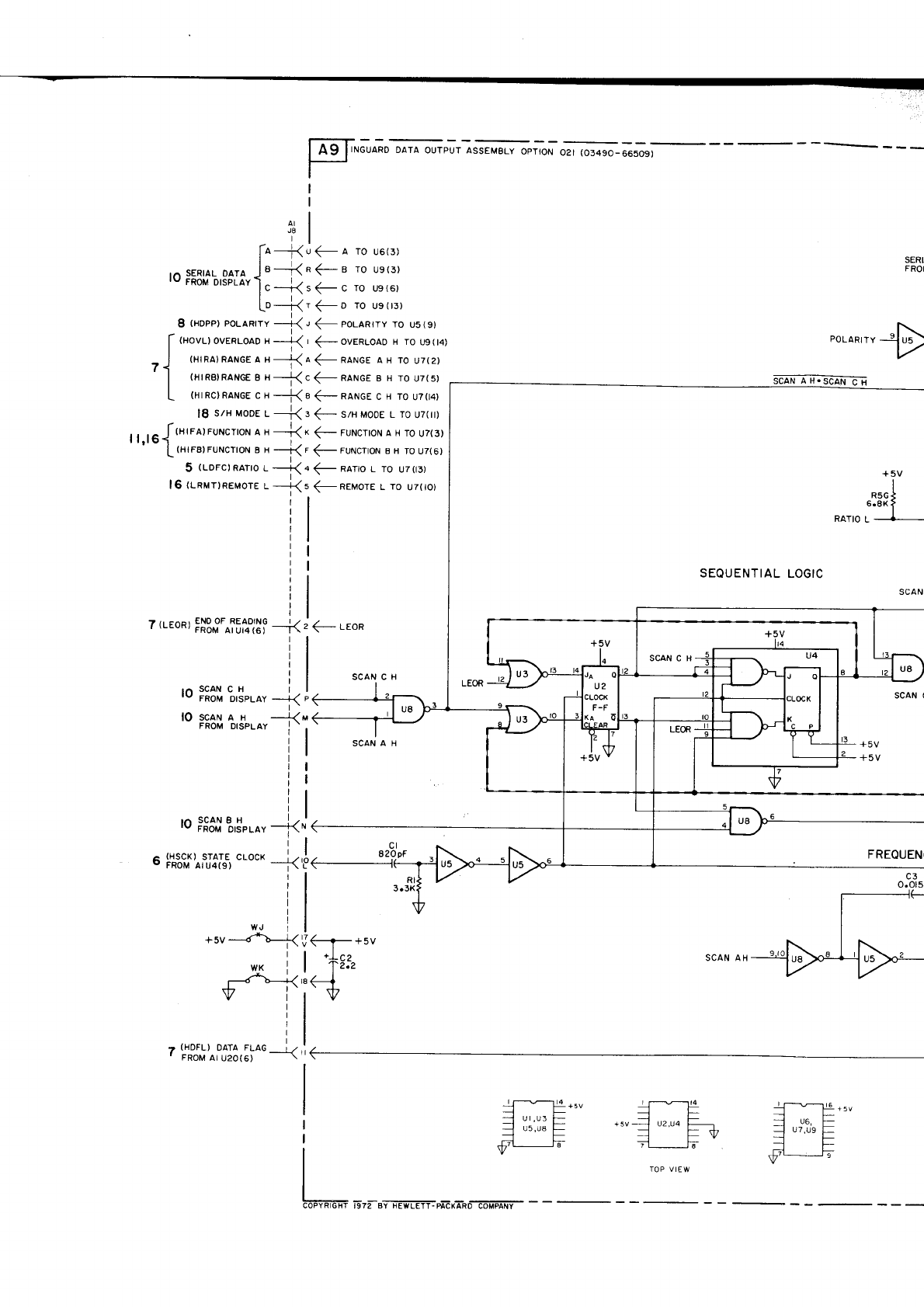
___
INGUARD
DATA
OUTPUT ASSEMBLY
OPTION
O2I
(O349O-65509)
J8
I
5 (LDFC)
RAlo L ---<
l6 (unur)RervorE
L
--<
\- a To u6(3)
f a ro usol
f c ro usret
<-D ro u9(r3)
f eolanrrv ro u5(9)
(-ovrnuoao H ro u904)
f nar'rOe a H TO
u7(z)
<- RANGE
B H TO
U7(5)
(- naruce
c H To
u7(14)
(- szH MooE L ro u7(r)
(- rurucrroru a H To
u7(3)
(- rurucrror
I H
To u7(6)
f narro
L To u7flJ)
(-neuore L ro u7(to)
SERI/
FRO!
8 (xopp)
,o.o",r, J
l- crovr-t ovERLoAD H
---<
Z .] (HrRA)
RANGE o , --f1
I txraatnaruce B
"-{
l- tHrnc)
Rrroe c H
--f(
16
sr" uooe
r_
{
I l,l
6
{tt'to)t"tt'o' o " --]1
' - [tlratruruclo'v a r --k
s
T
I
c
I
5
5
POLARITY
7
(LEoR)
Fil!""'^T[ä'läf
--j1, 3 r-eon
SEQUENTIAL
LOGIC
SCAN AH
lo
::äX'
?,3,.o,
-=k
lO scaru a x
FRoM DISPLAY 1
I
I
I
I
I
I
I
I
I
I
TnSCANBH l.t
'v FRoM otspLAy -14.
I
I
A (HscK)
srarE clocK t,
.
e FROM
atu4(9) ---n
I
I
I
I
I
wJl
+sv ---J4-!--LZ t\
SCAN C H
SCAN
A H
82OeF
RI
3.3K
FREQUEN(
c3
o.ot5
--l€--
+5V
I
wKl
--^--<
Vi
N(-
I
,8(_
I
I
I
'i<--r
| '+8:,
183
IV
z (HDFL) DATA
FLAG , t
' rnolt
ar
uzo(e)
IOP VIEW
aöFlElöITl5zzailEfr lETT:p-x-rnoror-priV-
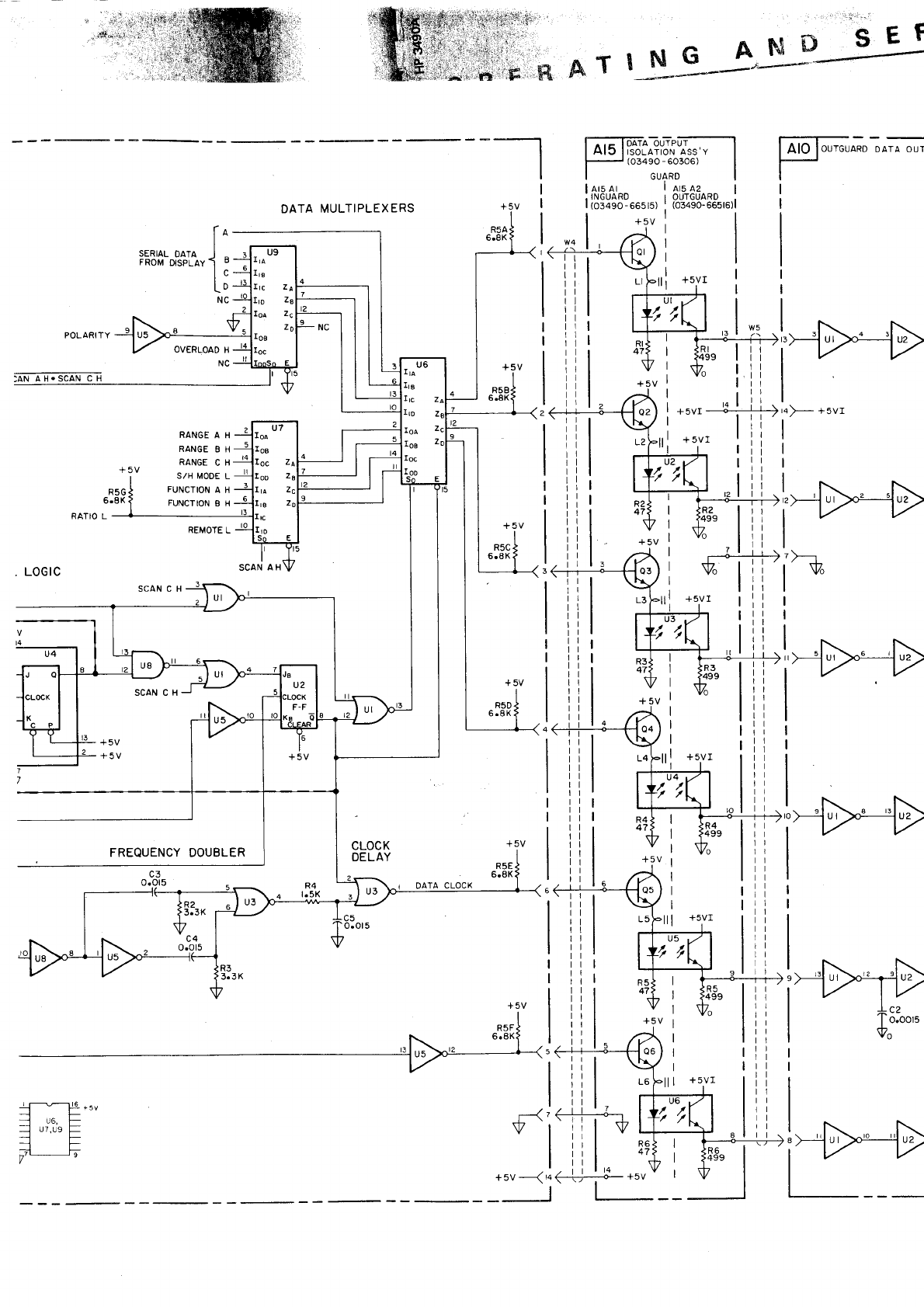
DATA
MULTIPLEXERS
I , . ,
.- ...:.i.
-. .
eTrNc- j,,s-$**
.qEf
F+ ' _-n
larsl$l^1.iil
-(o3aso-60306) I
I GIJARD I
lqrsar larsaz I
;
INGUARo I OUTGUARD
:
|
{o3490-665r5) : (03490-66516)l
,,
I Ä
,P
Ia
sERraL
DAra | -
rnou tlspray I ö
[;
OVERLOAD
H
NC
. LOGTC
FREQUENCY DOUBLER
c3
o.ot5
CLOCK
DELAY
roe
roc
roo
Ira
lre
Irc
Iro
:!---'19 +5v
__l u7,us
F
:lf
t7, '9
V
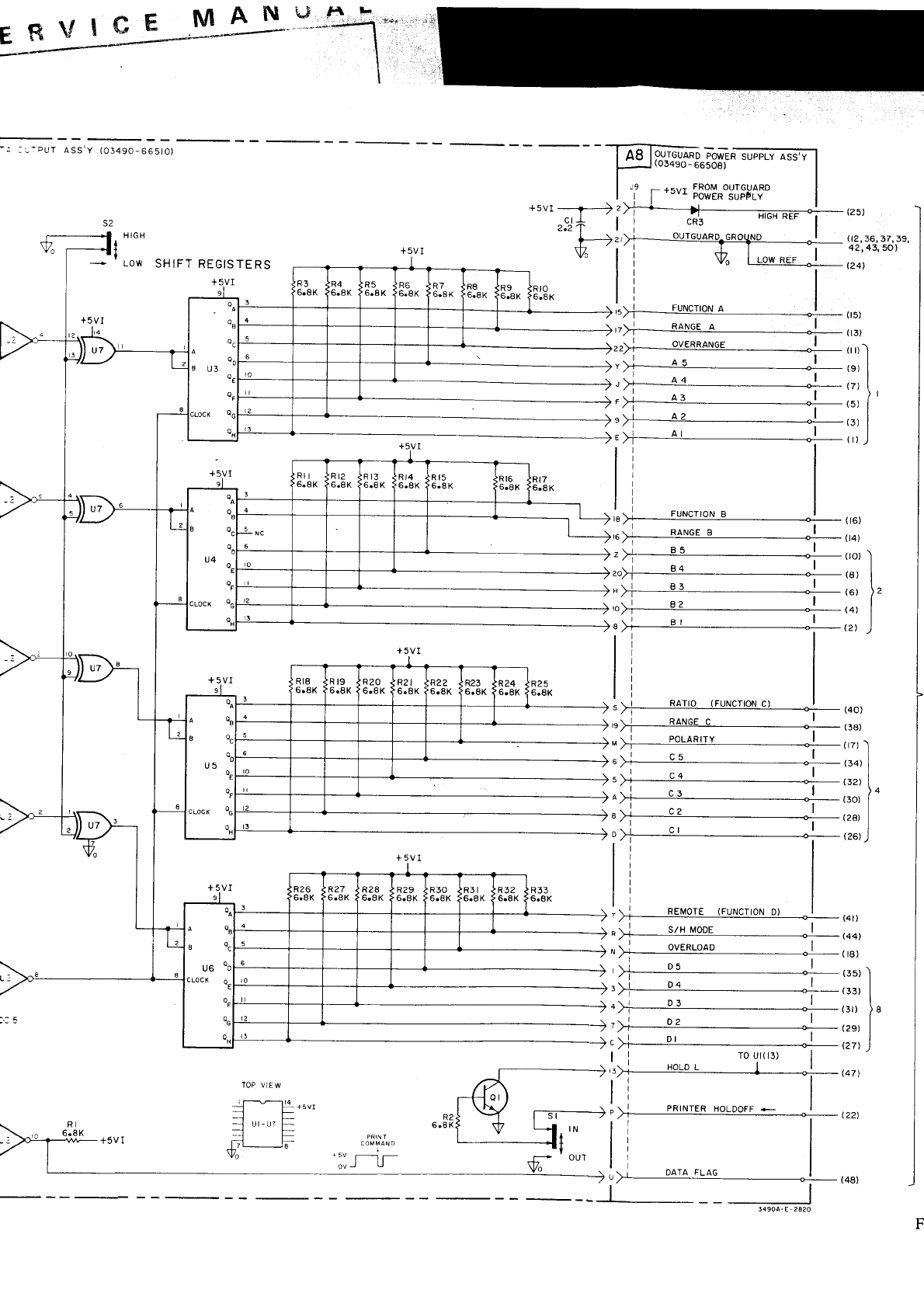
EG9\'ICE
F it
-NIANri fr. F
: --
our ass'Y
(01490-665tO) JTGUARD
POWER
SUPPLY ASS'Y
5490
-
56508)
r<,,t FROI OUrcuaRD
'"'. PowER
SUPFLY
+5vr
_r--) 2
,:,)+
.
I
ft2'
V. l
-'Low SHIFT
REGISTERS
(25)
(t2,36,37,39,
42,43, 50)
t24l
+5VI
'5%trst
PA^IAF ^ |
-\rJ'
22@11;y
,4rgr
lt
zfti-trorl
,">]-tL .! ,r, I
"f tu "l ,u,
!t
ro#1a1 |
.#,.,-J
l,
i
,^'"
,,,".'"- .,
"l
,.",
TOP VIEW
=tr
ll ur-uz
f
=F
Ttl_J-
%
^'^'. HIGH
REF
OUTGUARO^
GROUND
I(35)
I
(33)
I
(3r)
)
I
I
(2e)
I
t27)
)
(47
)
t22)
(48)
I i rour(r3) I
-\: HOLDL | |
i':
.T ! PRINTER
HOLDOFF
+ I
til
lil
l.. i DAra FLAG I
t-
+5VI
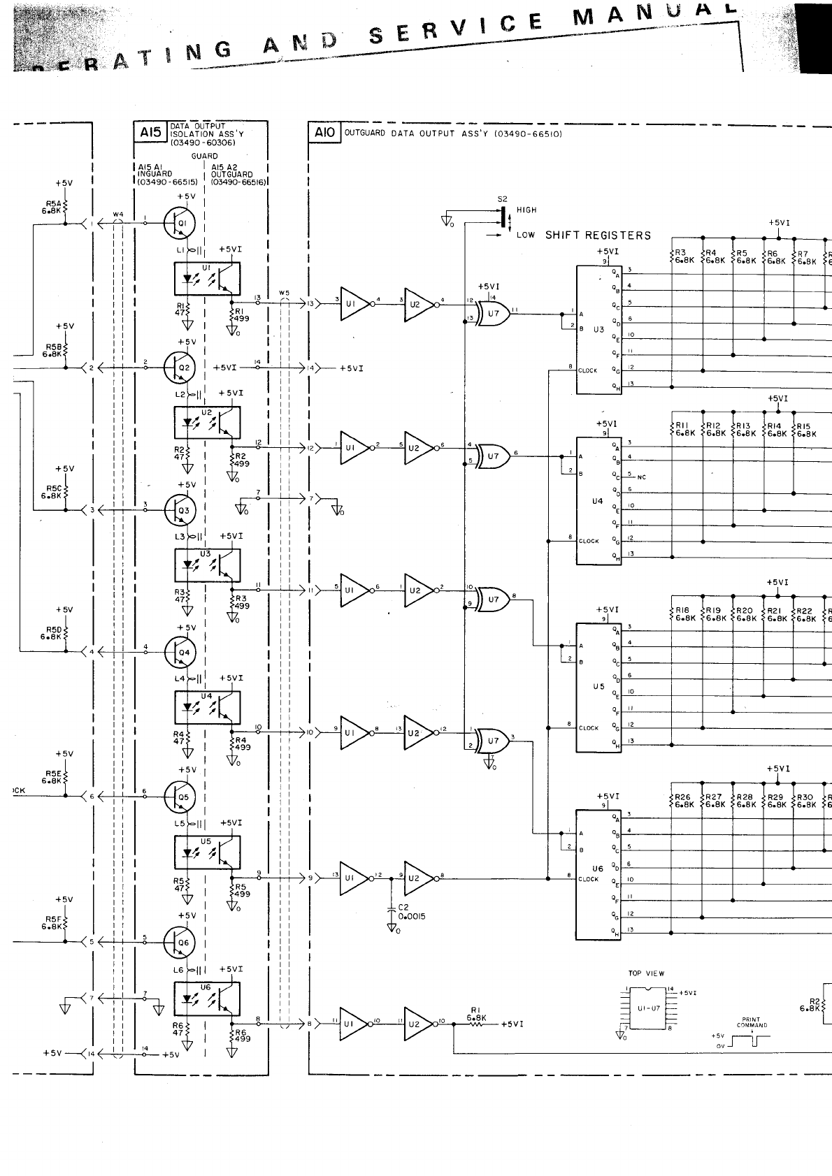
,-gj-l
*5V -{rq
I
R5Fl
6.aK>
r--<
v
I
s E
R v I j:-E MAN
&YghIG ANEi
* "]--*^--.'en'
(o3490
-60306)
GUARO
ar5 A2 |
OUTGUARO
:
(o3490-
665r6)l
a^
Qc
ac
oe
0_
QG
HIGH
LOW SHIFT REGISTERS
+5vr---1i1+;4
COMMAN D
*sv ---j-
I ll
5V+
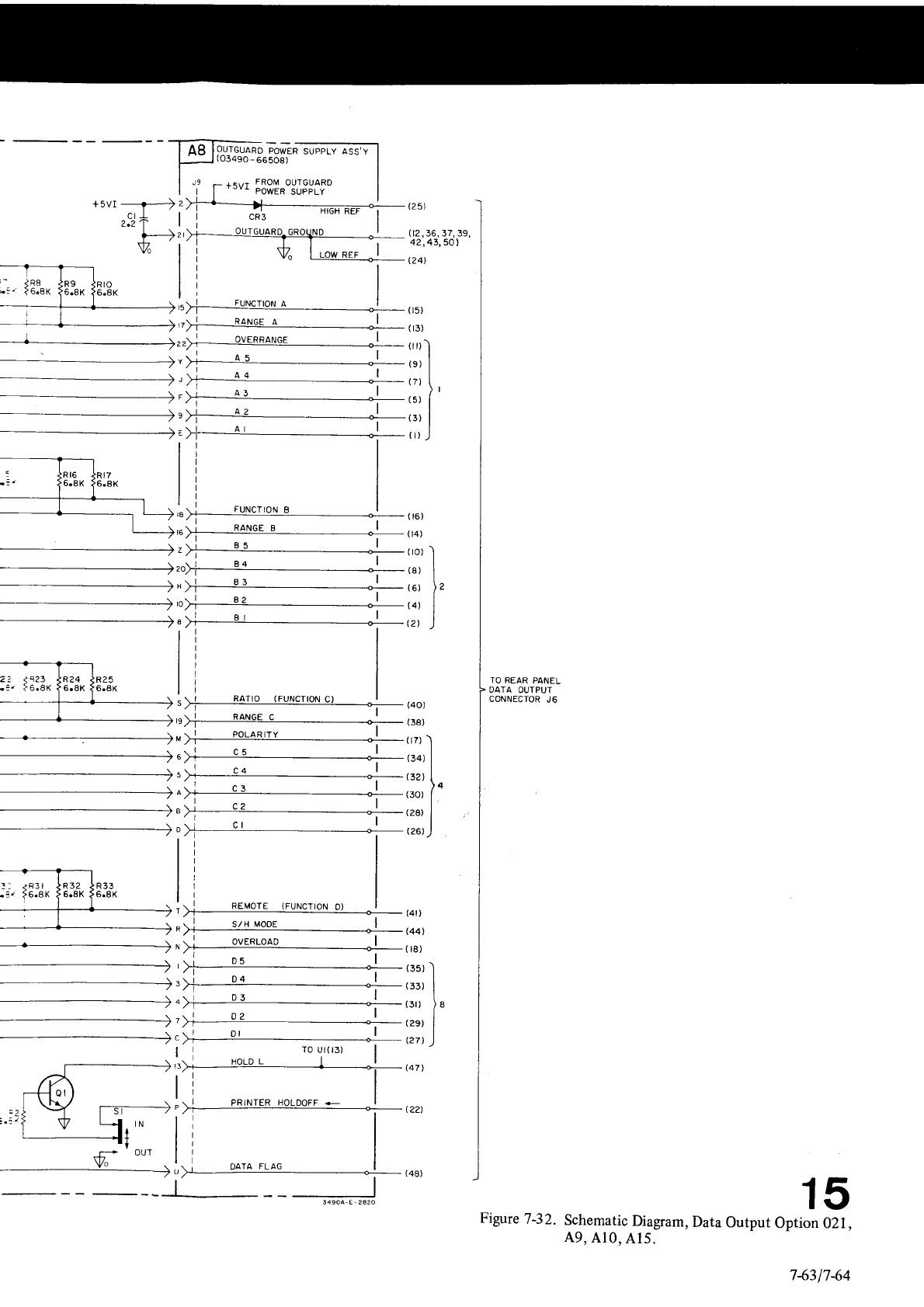
OUTGUARD
POWER
SUPPLY
ASS'Y
(o3490 - 6650S)
| ,,r,
.r, .,, ur,
| 42,43, 50
)
(
t6)
zfu*-rrot I
.o>i---qo .l ,rr I
*;| 83 "l 151
fz
,o+(4)l
.
>f--- a J ,r, J
,^r I RANGE C
''-{3ö,
-\
+5\/r FROTV
OUTGTJARD
' -' . POWER
SUPPLY
+svrt'2
,:)+
.
I
fr2'
V. I
\ \ ' DATA
FLAG I
7--r48t
OUT
V"
74317-64
TO
REAR PANEL
DATA
OUTPUT
CONNECTOR
J6
15
Figure
742. Schematic
Dagram,
Data
Output
Option 021,
49.
Al0.
A15.
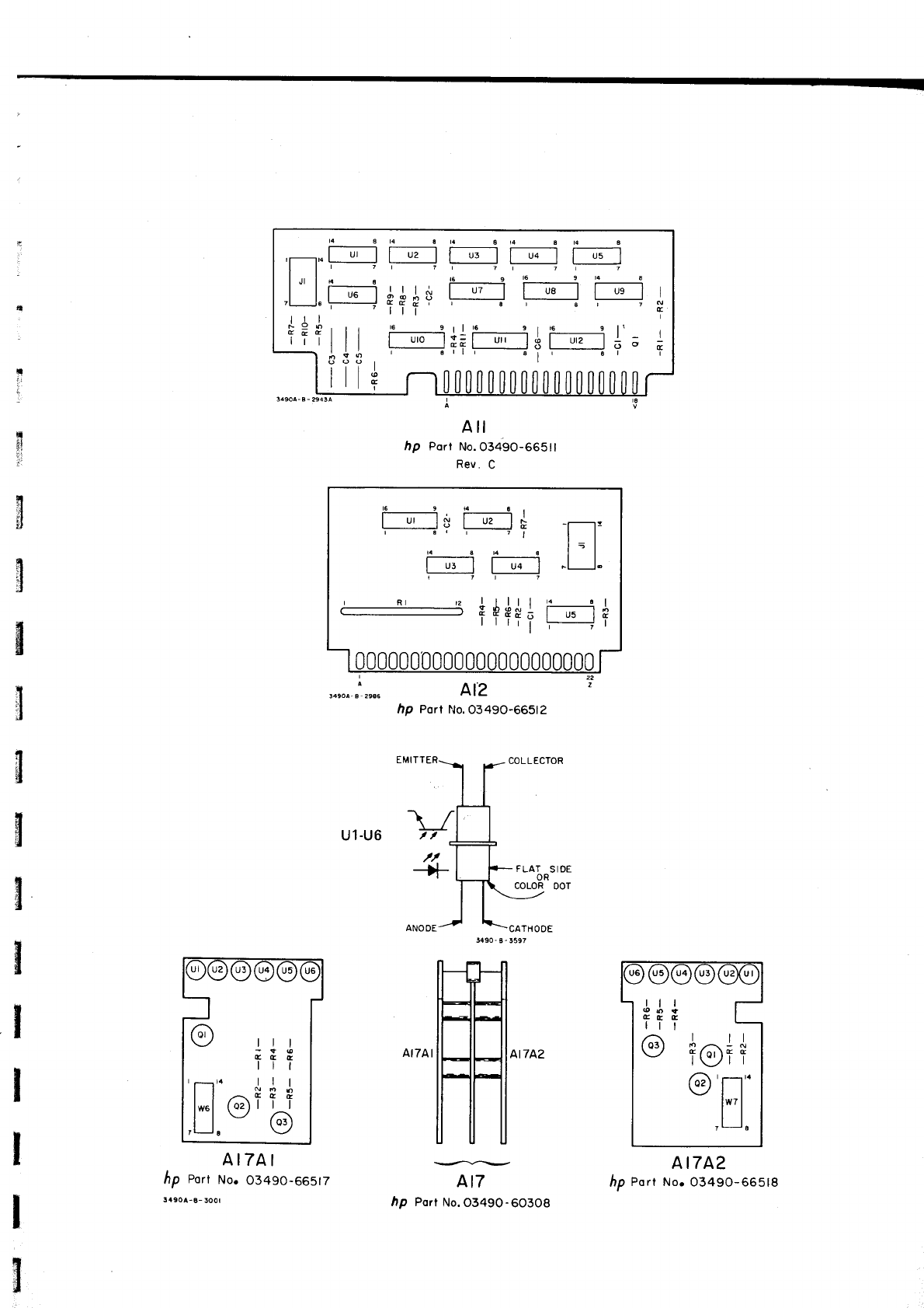
A tl
Htl
hp Pott
No.O349O-665t1
Rev.
C
,o.oo-"1.""" Al2
hp port
tJo,
03490-66512
FLAT SIDE
OR
coLoR 007
AITAI
hp Port
No. 03490-665t7
5490A-A- 5001
-At7
hp Port
No.
O349O-60308
At7A2
hp Port Noo
0349O-66518
169148,
r- ,x--l * f--,t-l *
r611 7l
148{6
r,il F;]
t7t7
ä----------jr-----q
* + +
J
J iu;i t
rrtl-l
I
6r
\-/ltl
;;E
ttl
rr rr. | | |
llNo6
| | /'\5 g q
l*"1
(:?' i{
| | (o3)
t''a \-./
ro**
@ Tr''
,[:]"
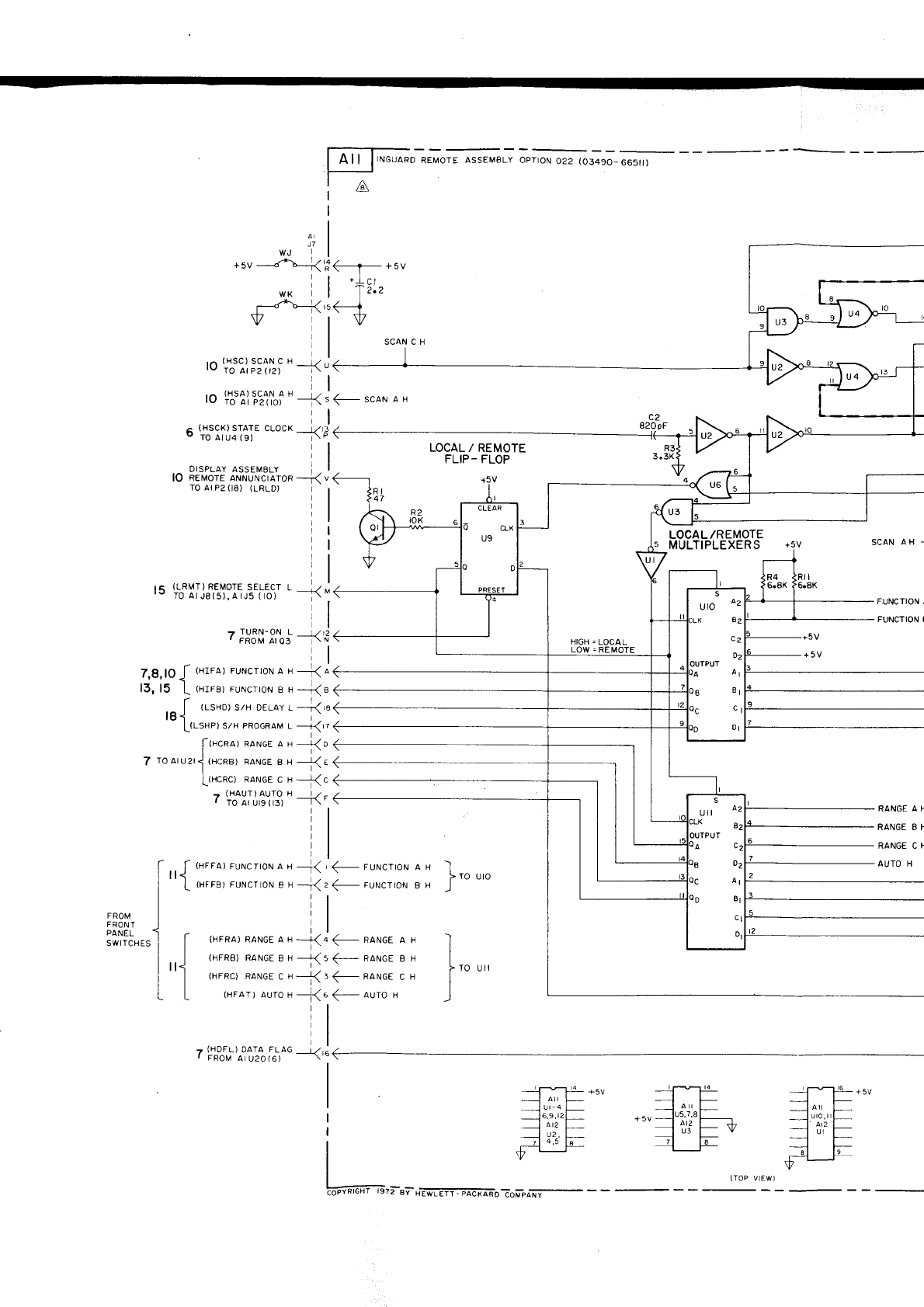
ff+sv
. Tr,,
t-J V
A
J7
wJl
t.
+5V < r-T<.
I
I
wKl
-A -(
\|/r
I
I
I
I A| | |TNGUARD
REMoTE
assEMBLy
oploN oz2 (o349o-665tr)
la
(- scar,r
n H
c2
82OpF
LOCAL / REMOTE
FLIP- FLOP
a5V
LOCAL/REMOTE
5 MULTIPLEXERS +5V SCAN A H
r^ (HSC)
SCAN C H __12
'v rO At
pZ
(rZ) |
\
I
I
,^ (HSA)SCANAH ,,I
tu ro At p2{to) ___\ s
il
A (HSCK)
STATE CLOCK
___L/
r
e Toatu4(9) r\P
DTSPLAY AssEMBLy i I
lO REMoTE
nruruur'rcraron
-f( .
TO AI P2
(I8) (LRLD}
t5(LRMT) REMOTE
SELECT
T0 arJS(5).ArJ5
tO)
RANGE
RANGE
RA NG€
AUTO
\-
<-
<-
s-
<-
s-
--ri
rl
ll
____J-/
t2
\N
tl
-{;
-k,u
I,
-r,'
--+( o
t/-
t\-
v
|
/-
--T-\ '
tl
il
;l
il
il
-T\'
il
ll
i
.l
--la"
tv
t\-
l/
---^5
RANGE A F]
RANGE 8 N
RANGE C I.1
AUTO H
FUNcroN a
H Iä
TO
UtO
FUNCTTON
B H -)
AH
BH
CH l-
,
r (HDFL)
DATA
FLAG | /,.
r FROt\i Atu20(6)
(ToP
vlEWl
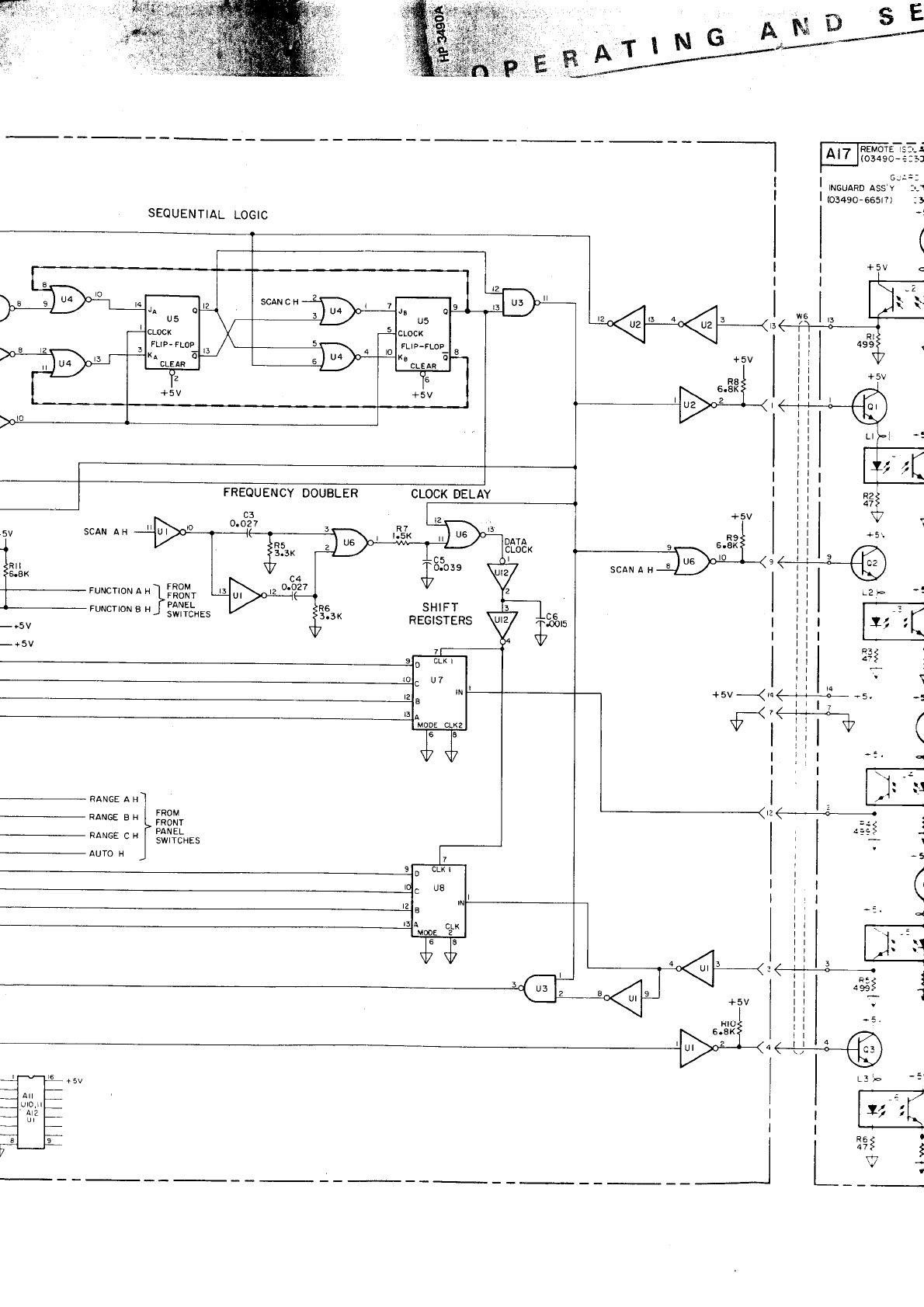
A
<Lv
> 9U r t--
l- n
ornv
tt"-'ttl,t3
|rc:euvu
-r'iöui
1
x
LH
v lgNvu
o ';- t ; i
\ l:l
),Allztr
/ 'r-__*5; >_jj'
;-
-'--Tilil'r^'.
r=:
lii I
\-----l
)'.'t
l
:- 421
su31sr93u
tl rHs
^v'130
)13013
> ^g+
I
;-
c: Q.rg99-06,90)
ri_ ^,ssv ouvngNl
ct90'1
tvtlNlnoSs
l=_?fi,ii!E!g
ä- ,TY
B
ä'
-.i
_,,:H
tfl* *-1-"v
Asffi
*1--s'-
sE,Rvt_- \d
\u
rihlq
I AJtlil;o-'*il1".i'I ;;;;,
GUARD
rruouano
ass'i'l oürnrono
oss'.,
I
(o349o-66517)
|
(o349o-665t8) |
U5
-FLOP
AR
5V
LOCK
DELAY
0.039
SHIFT
EGISTERS
5V
R5
499
\
+
V"
r500 t\
\^o
l/
+5VI
I
<R6
Ito*- -7u
-fl. u5
1,,
1*,
U2 9
-1 .-Ct
--J L
nBId
fl Tno
JU Aq+
?
oa
9NI|llvu90ud 3l,ot'l]u
sStsvNS oNV stou-j-Nol tlNvd
o8J S3l8VStO
t Ot SnOnNrlNO9
f
I
u3x3-rdtI"lnn
0uvn9rno
rns+
---<
I^S+
(8r999-o6rco)
| (
l,ssv
ouvngmo
I r
I
I
\I
':-',:.:
:
\16e I x 3'1
9yLlsyL
'zz0 uorldo
lndul
9r
.LIY
,ZIY
,IIY
olotuo1'ruur8erq
Jrleuor{cs'gg-1
arn8rg
(o€)1f 80tc3NNof, lndNl
3row3u t3NVd uvfa or ---r\ s
Jt I
?
oNvntroc
83X3"ldlI-lnf'l
ouvn9tno
oAl
z+l
.I
I
l.
IA9+
--+<
,"4
-
:! X^"
+
|
EJ
(.<-
- ^tddns ufMod
o ouvn9-l-no or
tf UoIS3NNOC
lndNl
l.!or'r38 13NVd Uv3U 01
IA9+
l-l8vN3 3IOI43U
+
Ftvu9oud H/s
H 3 39NVU
gNrnFrvu9oud
3row3u
sStevN3
oNv s-lou]-No3 tlNvd
INOUJ
S3-lgVSl0,l\Ol SnOnNllNO3
{e)--<
t'
i
i
I
I
I
I
lZZl
--+(zt
flz)-< r
(r)--< I
te){z
toz){r
(6r)-ko
rzr-k:
trr
-k e
(cz)+<
N.
(s)--<
n
I
otf
8v
""-]i::.
IA9
+
I
I
I
:::,
r:
:'.::.
;..':'
a,: I..
,,'' t,,..
:., l
;i::
:;:::
ir.;.
:i:.
i:,1,
1:j,
TO A2
LEX E
427
hp Port No. 03490- 66527
Rev.
B
ffiru1ün
ct2
ABCDEFHJKL
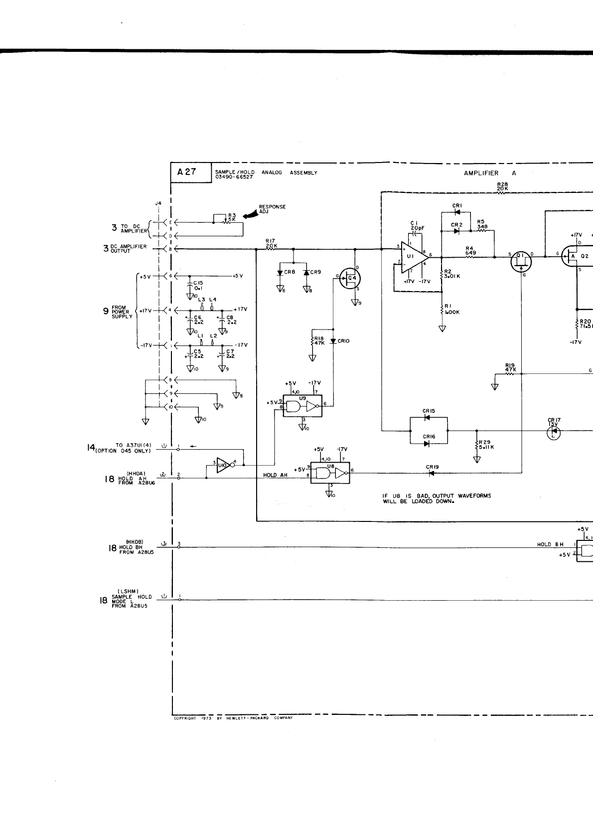
f]-atr+;;"., ^-**;;;
I
AMPLI FIER
IF U8 IS BAD. OUTPUT
WAVEFORMS
WILL BE LOAOEO DOWN.
, algR r/oo'
e F8fi8.
SUPPLY
14,0"'o*'%Ä'äuJJii
*
18
F8#"Äi.*
IHHOB)
l8
PRbou%'u.
-nv-f(I
I
I
l/
l---i
L---;<
L_t
+
.l
< r I ö r -'tu
.+!:.
+{,
II
pro ps
(
LSHM )
t8 iäB?'i
"o'o
FROM A28U5
I
I
COPYRIGflI I97] BY HEWLETI
- PACXAAO COMPÄNY
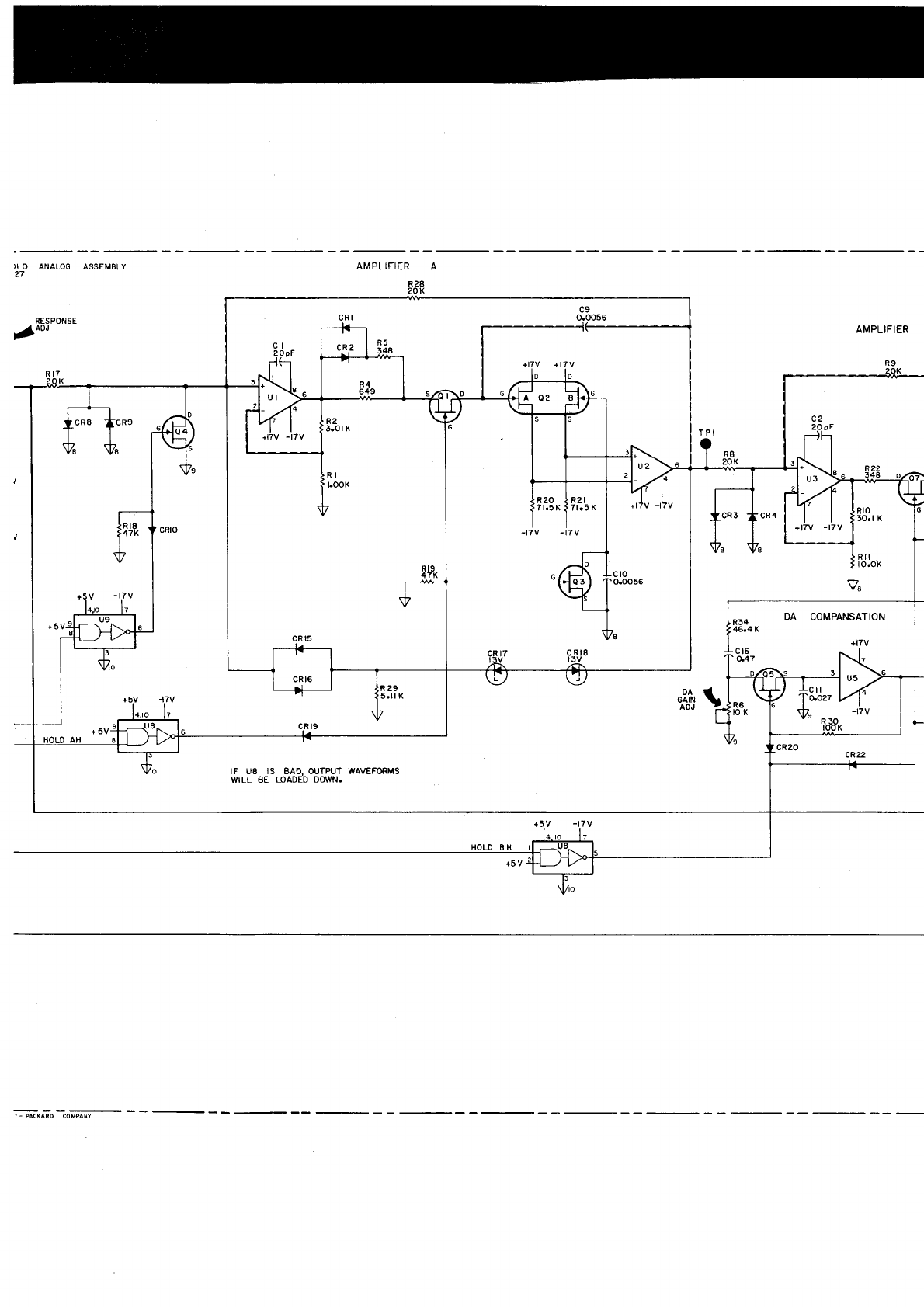
ASSEMSLY)LO ANAI"OG
27 AMPLIFIER
RESPONSE
lloo',
car{c*ol
I lrgS:,-
IF U8 IS BAD. OUTPUT WAVEFORMS
WILL 8E LOADED DOWN.
R34 DA
46.4 K
ct6
T- SC(AFO COMPAilY
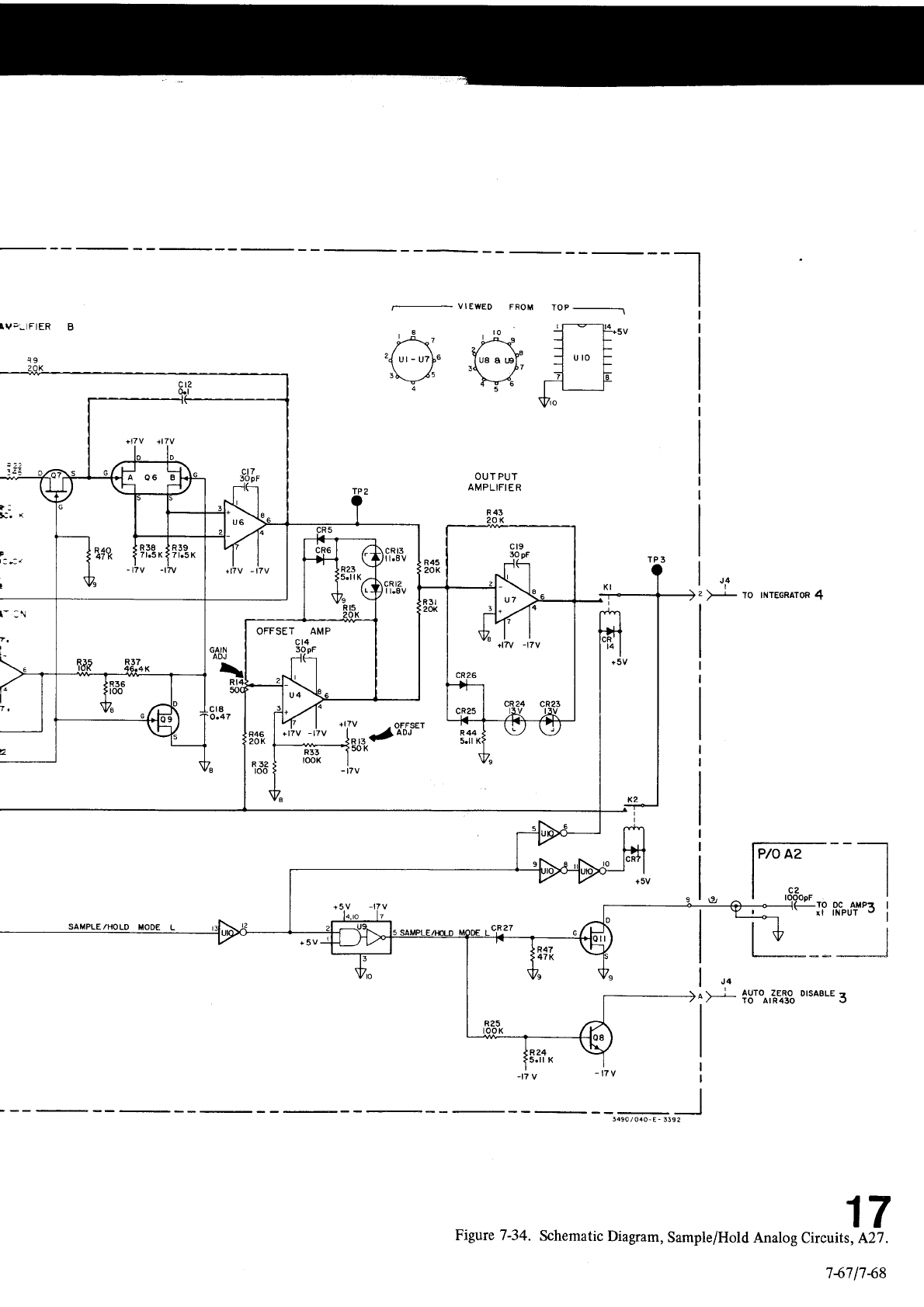
_ VIEWED FROM TOP_
'/ r, - rt\u {u. u *t'"
\/34F7
.V' V
,J4
*to
?
- OFFSET
{ao't
rrreenrroR
{
^+ +3too,ä119
DrsaBLE3
i?? l9L'.- i9i.?-
17
Figure 7-34. Schematic
Diagram,
Sample/Hold Analog
Circuits, A27.
747l7-68
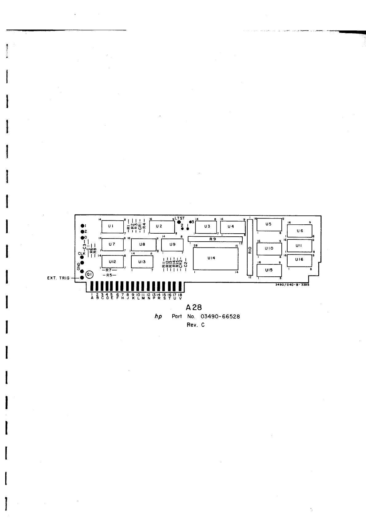
-"---
ut4
| €l---__-_-__19
luulH
i-----,l " l,
t69'6|---------.|9
l-l[l I u" I
I | ,' 'e
I-'"f-;'. l"
A28
Porf No. O349O-66528
Rev. C
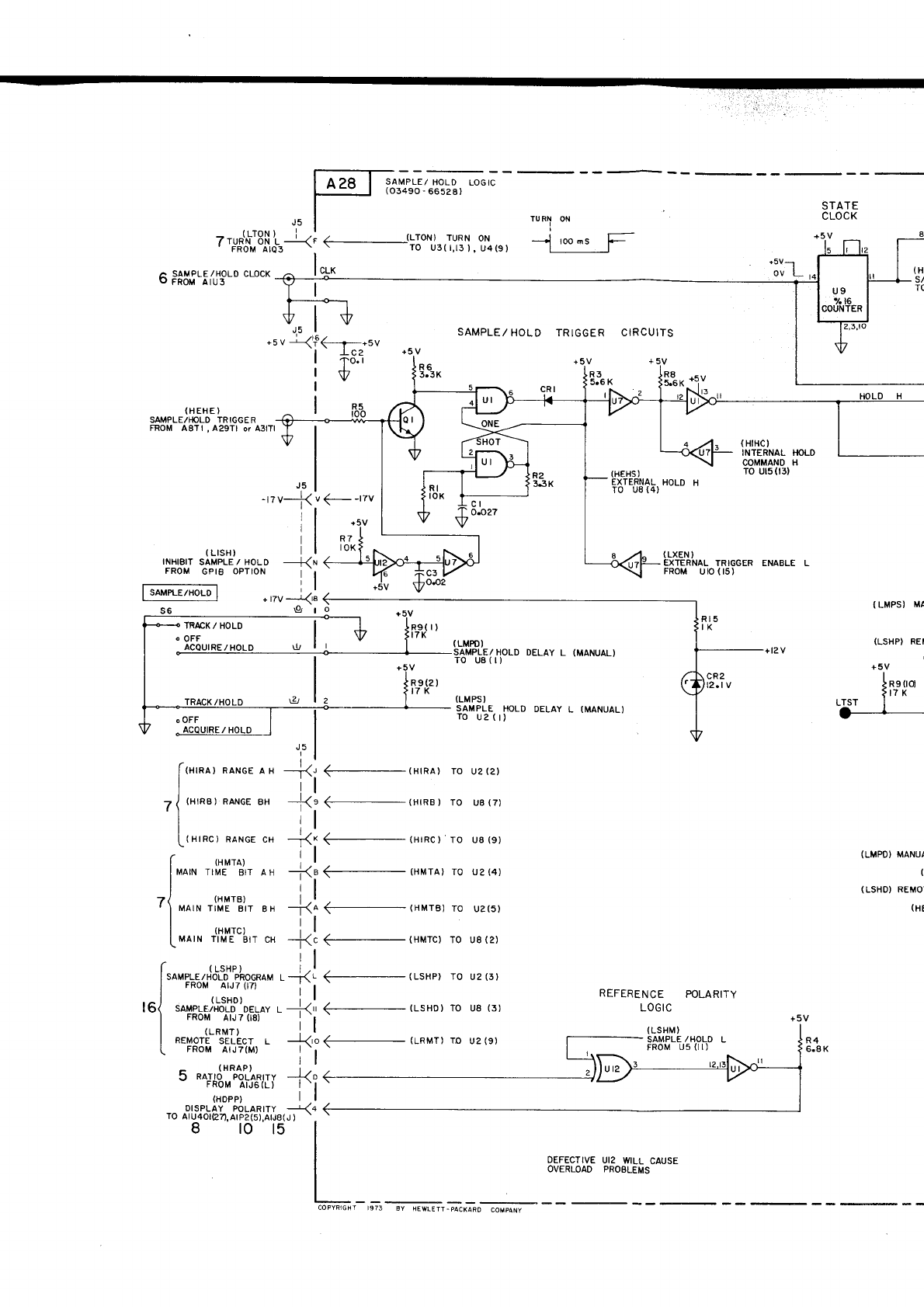
SAMPLE/ HOLD LOGIC
(o3490 -
66528)
J5 TURN ON
I
STATE
CLOCK
+5 V
- (LTONI " ,'
7'.'F$;
ö1,*.-<
F
<-(iäo*,j.,]lj!,j, ori",.,
|
..*
6 SAMPLE/H3OL0 CLOCK (H
s/
TC
SAMPLE/
HOLD TRIGGER
+5V
cRl
CIRCUITS
+
R3
5.6 K B.%*
tlu
(HEHE)
SAMPLE/IOLD TRIGGER
FROM AgTl ,
A29Tl or A3lTl
(
LSHD
)
(
LRMT
)
(LMPD)
SAMPLE/HOLD DELAY L (MANUAL)
TO U8il)
(LMPS)
SAMPLE HOLD DELAY L (MANUAL)
TO U2(t)
EXTERNAL
TRIGGER ENABLE
FROM UtO ils)
(
HrHCI
INTERNAL I|oLD
COMMANO
H
TO Ur5
03)
-,ru+
v
<_ _t7v
(LtsH) l_l
rNHrP.rT
SÄrrPLE
/_HO-!D ---KN
FRoM GP|B
oPTroN i 't
::::::::::=r i Isöä
FAMruwHorp-l
ll
R7
toK
( LMPS) MA
(LSHP) REi
(
+ 5V
l*rlo'
?
t7 K
-+
cR2
REFERENCE POLARITY
LOGIC
ILSHM)
SAMPLE
/HOLD L
FROM
U5
(I
I
)
(LMPD) MANU!
t
(LSHD) REMO'
(HE
t6 soH^.JrbÜlo.e-.av
r-
{' €- (L5HD)
ro uB
(3)
FRoM A|JT
(t8) | 'r
il
ner'lori-
öElbcr r_ -{'o <- (LRMr)
ro u2
(s)
FROM A|JT(M) | ',
il
- (HRAP) i.'
c 'TABu'?,'.ffiIi
f?
il
DlsPLAy poLARtt,t --4q
TO
ArU40t(27),AtP2(5).atJe(
J
)
R4
6.8 K
DEFECTIVE UI2 WILL CAUSE
OVERLOAD PROSLEMS
I973 BY BEWLETT.PAC(ARO COMPANY
ttl
Y,
l v
.sv {i6(---1-*sv
I rcz
. t.l
f
txtnat
nrt66
o t J, (H1RA)
ro uz(z)
lll
7 ( (HIRB)
RANGE
BH --j<: <- (HIRB
) ro uB
(7)
l:l
[,tnrnct RANGE
cH -i(l C- (HrRc)
ro us
(s)
( (HMrA) I I
luatl
rtue rirr ar -j{u (- (HMra)
ro u2(4)
.) (HMrB) i I
' ) r"rnrn
riue
ejr e
x -K^ (- (HMrB)
ro Uz(5)
| ,ru-., | |
LMATN
r|ME
brr cx {c <-(HMrc} ro u8(2)
8to15
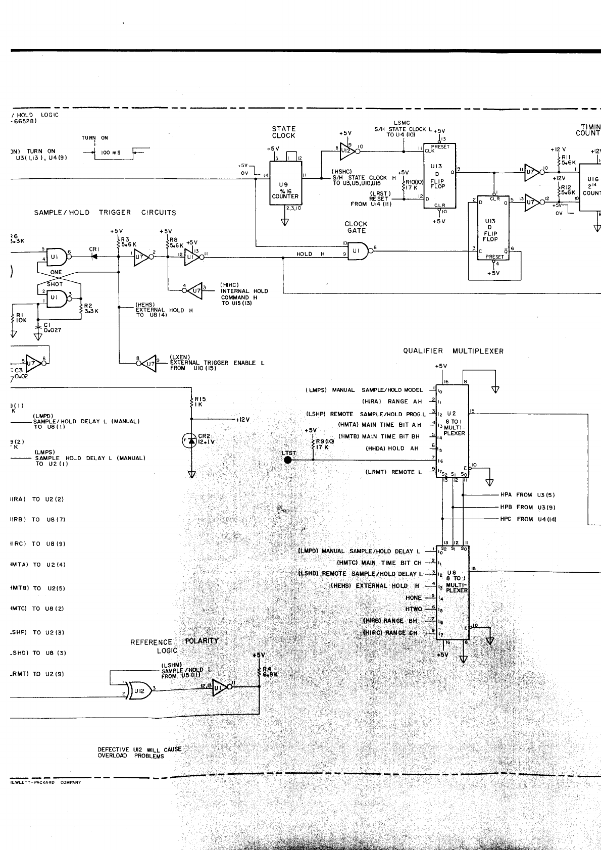
/ HOLD LOG IC
-
66528)
]N) TURN ON
u3(r,r3),
u4(9)
CTATF
CLOCK
TURN ON
ut6
2t4
couN'l
SAMPLE/
HOLD TRIGGER C IR CUITS
+5V +
E5
5.6 K R8
5.6 Kr3
QUALIFIER
MULTIPLEXER
!!Bs-u | ,
SAMPLE/Hq-D MODEL
(HIRA) RANGE AH
(
LMPO
)
-SAMPLE/HOLD DELAY L (MANUAL)
TO U8il)
9(2)
'K (LMPS)
- SAMPLE HOLD DELAY L (MANUAL)
TO
U2(t)
ilRA) TO U2(2)
IRB
) TO U8
(7)
ilRC) TO U8(9)
IMTA)
TO U2
(4)
{MTB)
TO U2(5)
{MTC)
TO U8
(2)
-sHP) TO U2
(3)
R EFI
-sHo) To u8 (3)
cR2
(LSHP} REMOTE SAMPLE/HOLD PROG,L
(HMTA} MAIN TIME BIT AH
+5V
n,'j
(HMTB}
MAIN TIME
BIT
BH
Rs(O
I7 K (HHoA)
HoLD
AH
(LRMT} REMOTE
L
S-*l:
HPA
FROM
U3(5)
HPB
FROM
U3(9)
HPC FROM
U4(I4)
I
,,'
(LMPDI }IANUAL SAMPLE/HOLD
DELAY L
(HMTCI
tlAlN TIME 8lT CH
: ;.' ;1:', ..i.:,ilgxot IREMoJE s4rrpLE,/Ho!-D DELAY L
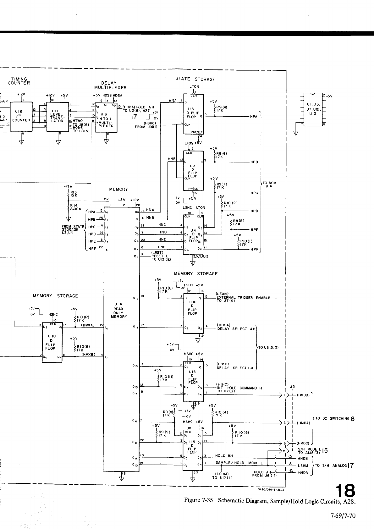
DELAY
MULTI
PLEX
ER
I5V HOSE
HDSA
utl
LEVEL
TRAN
S
-
LATOR
STATE STORAGE
LTON
L€<
IIOLD A H
TO
U2(6), A27 .sv
17 -fou
FROM UgO
R9 (6)
t7K
TO ROM
ut4
+5v
-..l
ovL
MEMORY
R9(5)
r7K
LSHC LTON
R ro
(2)
t7K
I
ISTORAGE
+5V
MEMORY STORAGE
+5V
- (LEXN)
I5 EXTERNAL
TRIGGER
ENABLE
TO U7(9)
{
Hr HC)
INT IIOLD
COMMAND
H
TO
U7(3)
"u-l
Rro
(7)
t7K (HDSA) \
DELAY
sELEcr aHl
I
lro
u6(3,t3)
(HDSB) I
DELAY SELECT
BH
J
I
>(HMDB)
i
t-
I
I
I
Rto(6)
t7K
E/ HOLD MODE
L
+5V
-] r5v {nrolat
Lov ?l7K l']-,,",.,
To Dc swtrcHtNc
I
r__+
".
>- ?6'
^Tr%r,..
i I
5
HOLDBH I r I.r,
Hn"oel
sauplezrolo
uoor
I I I | 'l lrru lto srr aruar-ocl/
,l..,lyl
, .[?.,f
4'6-ie- *'^
-J
toM
ue
(tst | "-" )
--,*J 1g
Figure
7-35. Schematic
Diagam, Sample/Hold
Logic
Circuits, A2g.
74917-70
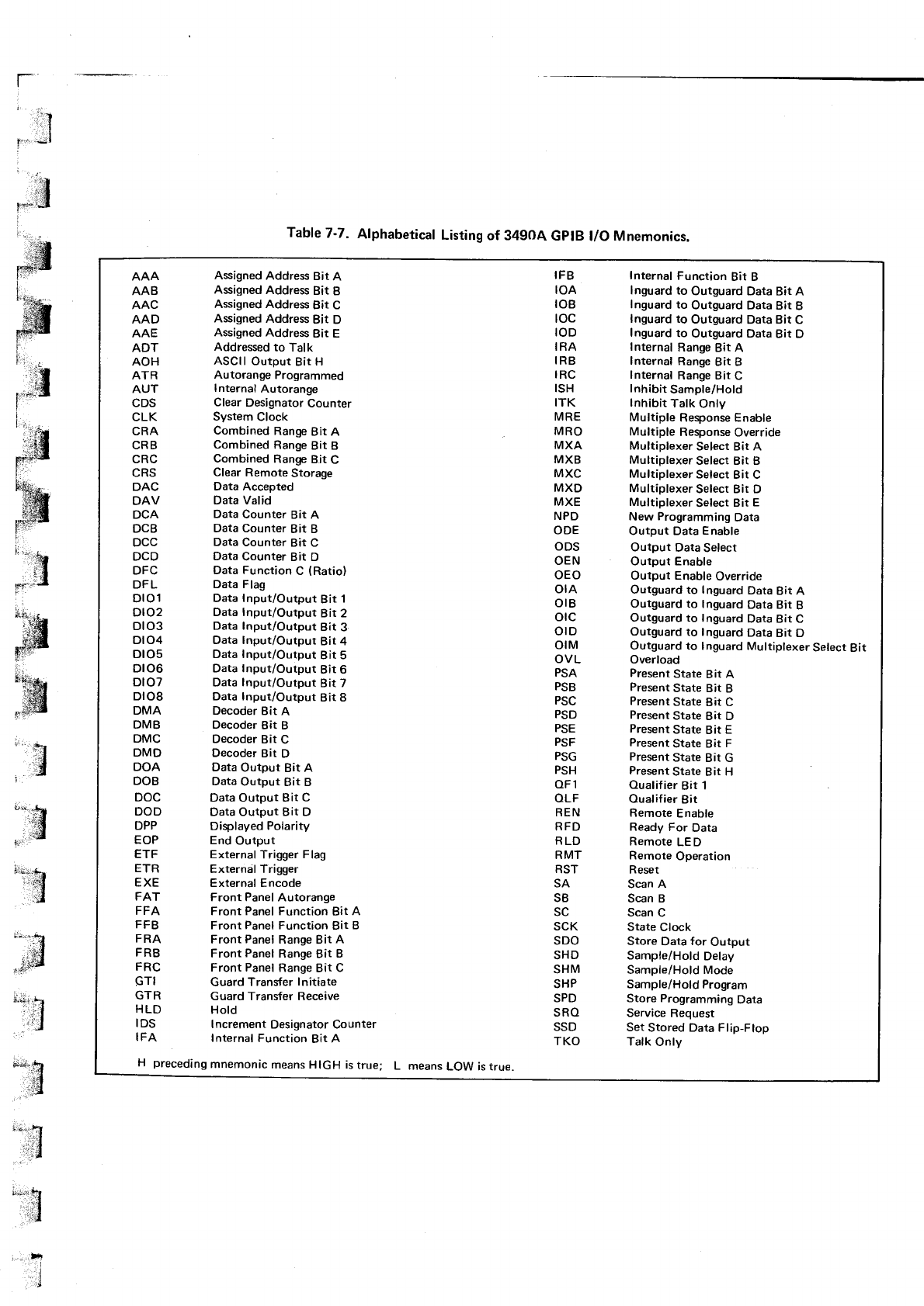
jil
;l
ä
f-
I
r'"
:
i_
t"
j
:l "..,
.:a.
:::;:
TableT-7.
Alphabetical
Listing
of 349OA
GplB l/O Mnemonics.
AAA
AAB
AAC
AAD
AAE
ADT
AOH
ATR
AUT
CDS
CLK
CRA
CRB
cRc
cRs
DAC
DAV
DCA
DCB
DCC
DCD
DFC
DFL
Drol
Dto2
Dl03
Dl04
Dto5
Dt06
DloT
DroS
DMA
DMB
DMC
DMD
DOA
DOB
DOC
DOD
DPP
EOP
ETF
ETR
EXE
FAT
FFA
FFB
FRA
FR8
FRC
GTI
GTR
HLD
IDS
IFA
Assigned
Address Bit A
Assigned
Address Bit B
Assigned Address Bit C
Assigned
Address Bit D
Assigned
Address Bit E
Addressed
to Talk
ASCII Output Bit H
Autorange Programmed
I nternal Autorange
Clear Designator
Counter
System Clock
Combined
Range
Bit A
Combined
Range
Bit B
Combined Range
Bit C
Clear Remote Storage
Data Acceoted
Data Valid
Data Counter Bit A
Data Counter
Bit B
Data Counter Bit C
Data Counter Bit D
Data Function C (Ratio)
Data Flag
Data Input/Outpur Bit 1
Data Input/Output Bit 2
Data Input/Output Bit 3
Data lnput/Output Bit 4
Data Input/Output Bit 5
Data Input/Output Bit 6
Data
Input/Output Bit 7
Data Input/Output Bit 8
Decoder Bit A
Decoder Bit B
Decoder Bit C
Decoder Bit D
Data Output Bit A
Data
Output Bit B
Data Output Bir C
Data Output 8it D
Displayed Polarity
End Output
External
Trigger
Flag
Externäl Trigger
External Encode
Front Panel Autorange
Front Panel Function Bit A
Front Panel Function Bit B
Front Panel
Range
Bit A
Front Panel
Range
Bit B
Front Panel
Range
Bit C
Guard Transfer I
nitiate
Guard Transfer Receive
Hold
I ncrement Designator Counter
Internal
Function Bit A
Internal
Function Bit B
lnguard to Outguard Data Bit A
Inguard to Outguard Data Bit B
lnguard to Outguard Data Bit C
Inguard to Out$rard Data Bit D
Internal Range
Bit A
Internal Range
Bit B
lnternal Range Bit C
Inhibit Sample/Hold
lnhibit Talk Only
Multiple Response Enable
Multiple Response
Override
Multiplexer Select Bit A
Multiplexer
Select Bit B
Multiplexer
Select
Bit C
Multiplexer
Select Bit D
Multiplexer
Select
Bit E
New Programming Data
Output Data
Enable
Output Data Select
Output Enable
Output Enable Override
Outguard to Inguard Data Bit A
Outguard to lnguard Data Bit B
Outguard to Inguard Data Bit C
Outguard to Inguard Data Bit D
Outguard
to lnguard
Multiplexer
Select
Bit
Overload
Present
State Bit A
Present
State Bit B
Present
State Bit C
Present
State Bit D
Present
State Bit E
Present
State Bit F
Present
State Bit G
Present
State Bit H
Oualif
ier
Bit 1
Oualifier
Bit
Remote
Enable
Ready For Data
Remote LE D
Remote Ooeration
Reset
Scan
A
Scan B
Scan C
State Clock
Store Data for Output
Sample/Hold
Delay
Sample/Hold Mode
Sample/Hold Program
Store Programming Data
Service Request
Set
Stored Data Flip-Ftop
Talk Only
IFB
toA
toB
toc
toD
IRA
IRB
rRc
lsH
ITK
MRE
MRO
MXA
MXB
MXC
MXD
MXE
NPD
ODE
ODS
OEN
oEo
orA
orB
orc
oro
otM
OVL
PSA
PSB
PSC
PSD
PSE
PSF
PSG
PSH
oF1
OLF
REN
RFD
RLD
RMT
RST
SA
SB
SC
SCK
sDo
SHD
SHM
SHP
SPD
SRO
SSD
TKO
H preceding
mnemonic
means HIGH is
true; L means
LOW is true.
;ä
*,'$
".ä
_;3
1ä
,..r1
-J
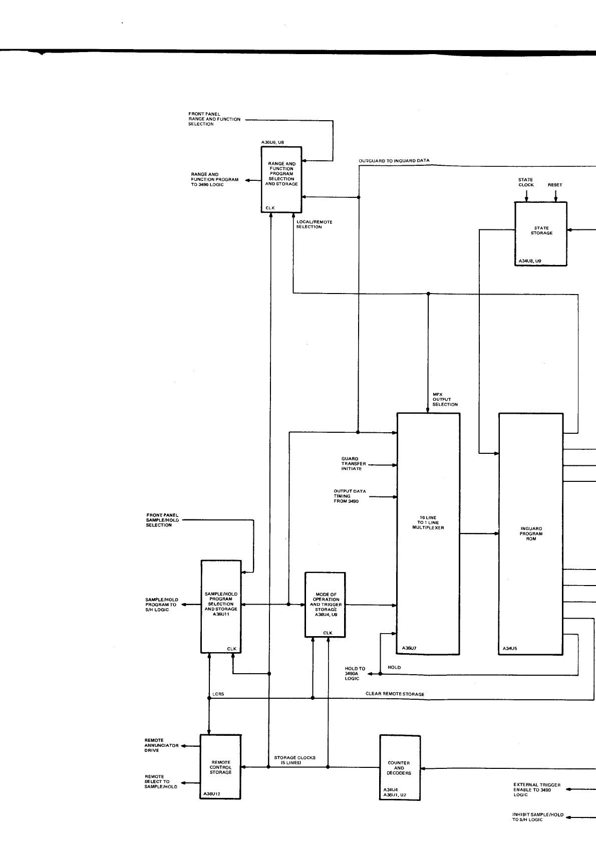
OUTGUARD TO INGUARO
DATA
STATE
CLOCK
LOCAL/REMOTE
SELECTION
I6 LINE
TO I LINE
MULTIPLEXEF
REMOTE
ANNUNCIATOA
DRIVE
AEMOTE
SELECT TO
SAMPLE/HOLO EXTEBNAL
TRIGGEF
ENABLETOg9O +
LOGIC
INHIBITSAMPLE/HOLO,
TO S/H LOGIC
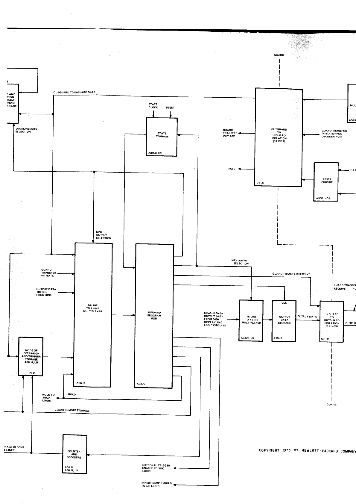
'.. '
OUTGUANO TO INGUAAO DATA
STATE
CL@K RESET
SLECTtOil
MENUFEMENT
OUNUT DATA
FnoM gs
DISLAY AND
LOGIC
CIRCUIE
GUARO
TRANSFER
RECEIVE
I
ouo"o
r"^n".,
I REcErw
I
'AAGE CLOCKS
5 LINES'
EXIERNAL TFIGGEA
ENABLE TO g9O
LOGIC
INHIAIT
SAMPLE/HOLD
TOS/H LOGIC
LOCAL/REMOTE
$ECTION
I6 LINE
TO 1
LINE
MULTIPLEXEF
COUNTER
oEcooERS
434U4
ASUI, u2
COPYRIGHT
t973 BY HEWLETT-PACKARO
COMPANY
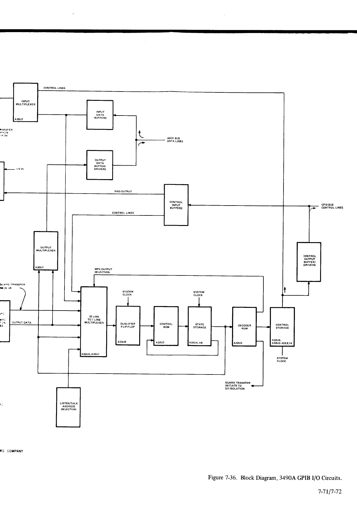
CONTROL
LINES
L. TD IRANSFE
R
f=w
LISTEN,TALK
ADDRE$
SELECTION
GPIE AUS
@NTROL LINES
Figure
7-36. Block
Diagram
,3490A
GPIB
VO
Circuits.
SY$EM
CL@K
FC COMPANY
7-7117-72
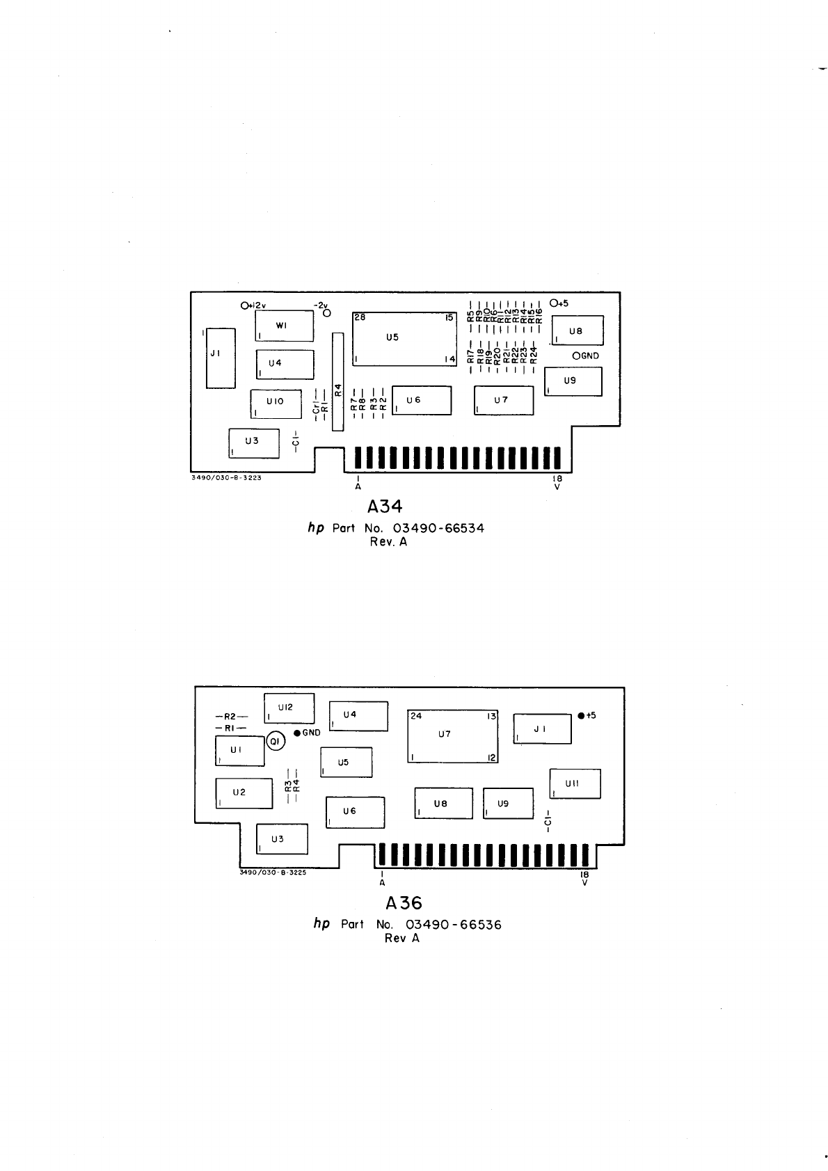
O+5
FI
OGND
E
ililililililnil11
I
hp Port
434
No. O349O-66534
Rev.
A
hp Porr 436
N0.03490-66536
Rev
A
l24-----r3-l [---l or5
I ut I l' '' I
l, ,rl
L
kt trlE
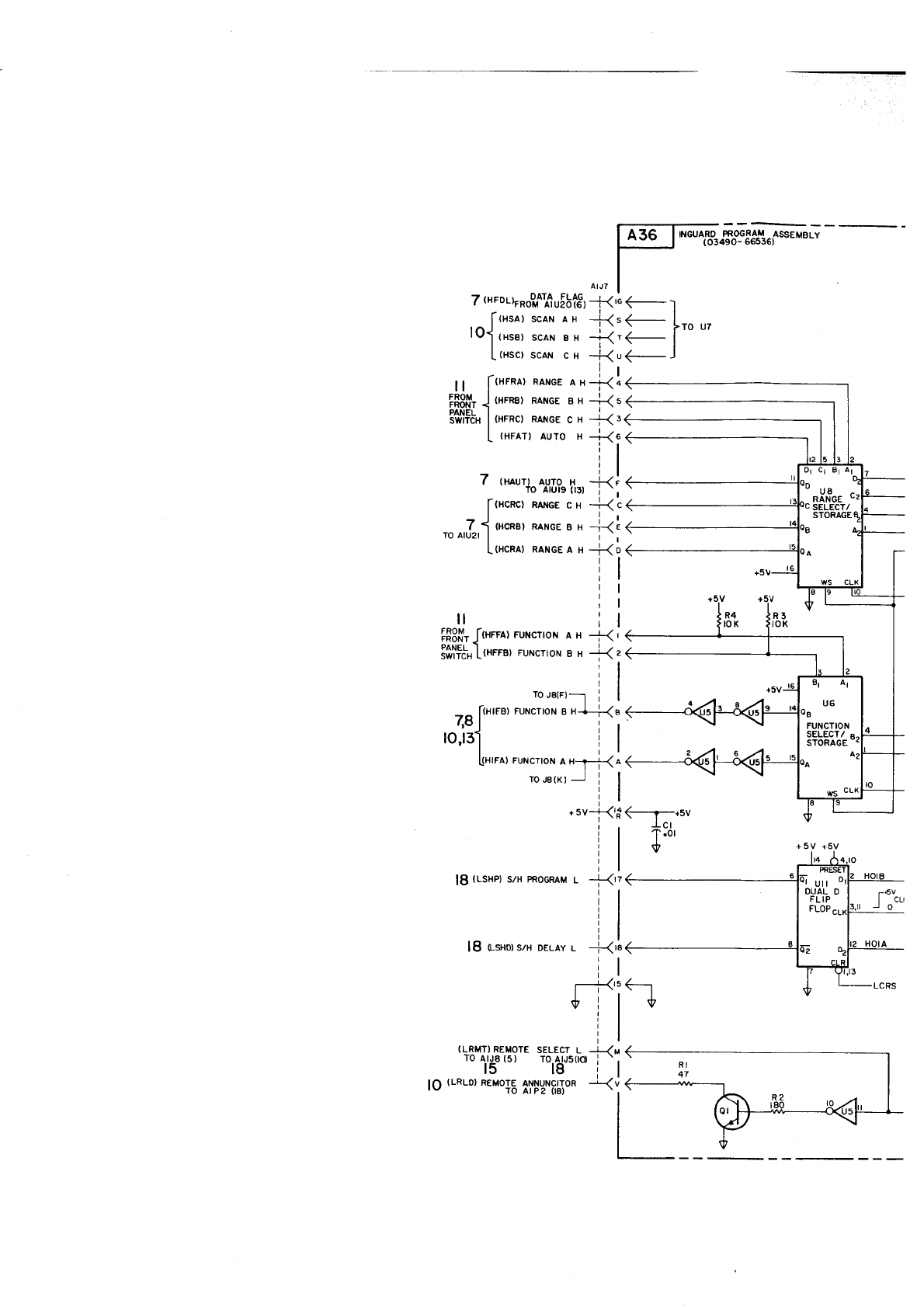
;>- rol98rfii'lV
9io"rr
(orurr
Ol
li Br sl
' \ i or)gntv or (9)
8flv o1
n)---t- 1 I3313S
31Oft3U
(IftU'l)
'l lv"llo H/s
(oHsx I I
'r frvueoud
xzs
tansrt
8l
A9+
A9
+
-
{}}9r or
x
v norrclnr
tvrul
fe
t'ot
le2
{ € NOU.]NnJ
(SJHU
-(J)8r
Or
s NorroNnr
rerrnrlH-.3J.rl!f5
v NorroNnr
rvrrxrJ
rfillj
il
o>-i-Hv3eNvu (v8cH)l
'. I lrznrvor
i>its3eNvuteucx)fZ
.+ Hc:cr.rvu
{cucx}J
t. i (er)
6rnrv or
i-- H
ornv
(rnvH)
z
tl
ri
r>t- r ornv
trv:Hl
'l
'\+- , c teNvu
tcu:xr
I tt11;193
t X- r s 3eNvu
rsurxr
I rffil
^"'tn*ro(ttn?3oo%lo%ttono*
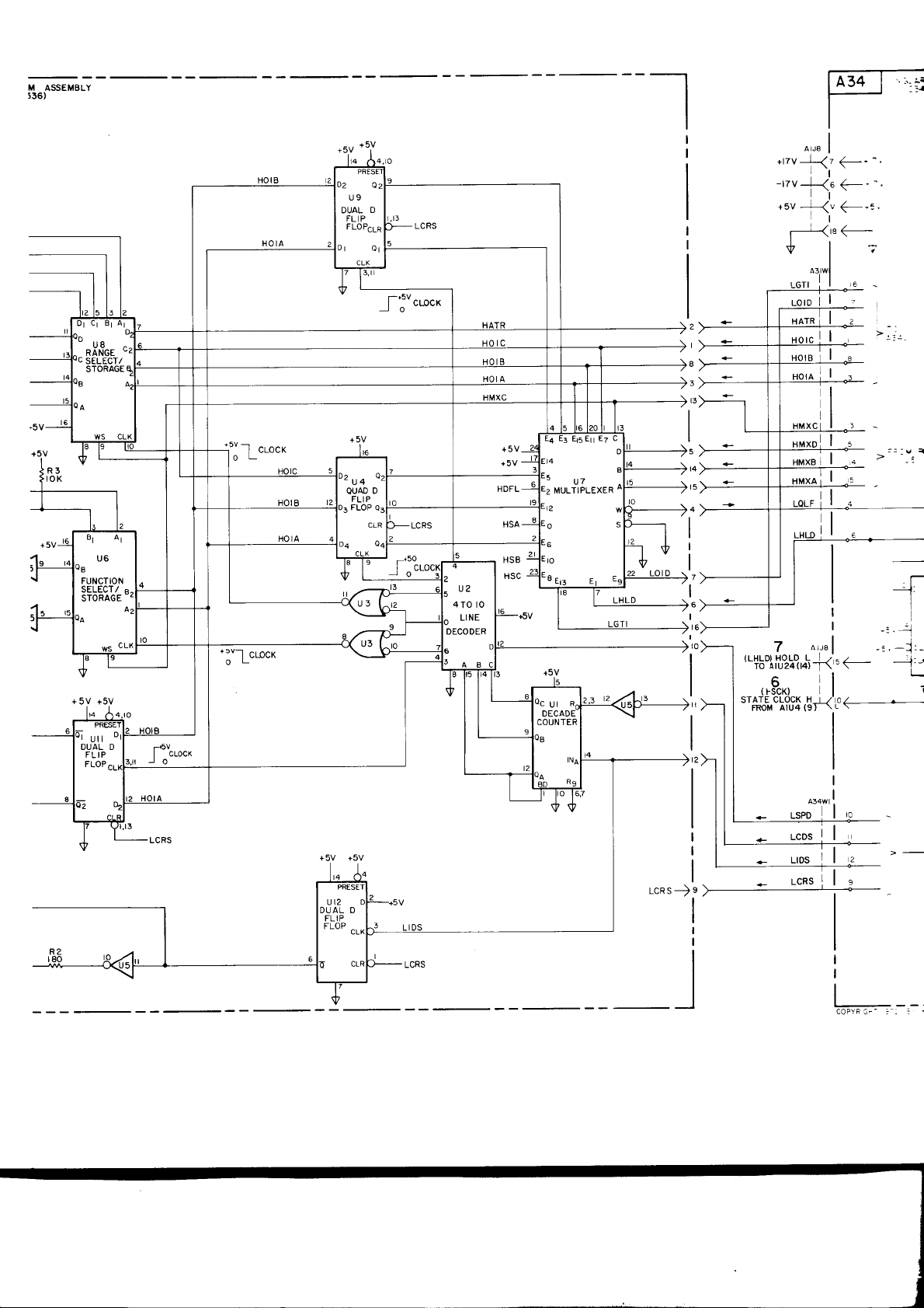
I i sosr
I
so
^ t,
v 83x3'ldlr'ln$l z
s9l
0
3 23 ll39Q €
Ltf
--)r,H
.,---2
n!-f nn*
-
-) slinur-
-
--) zf ,rzr*
I ertv
(9C!
l'rstl3ssv tt
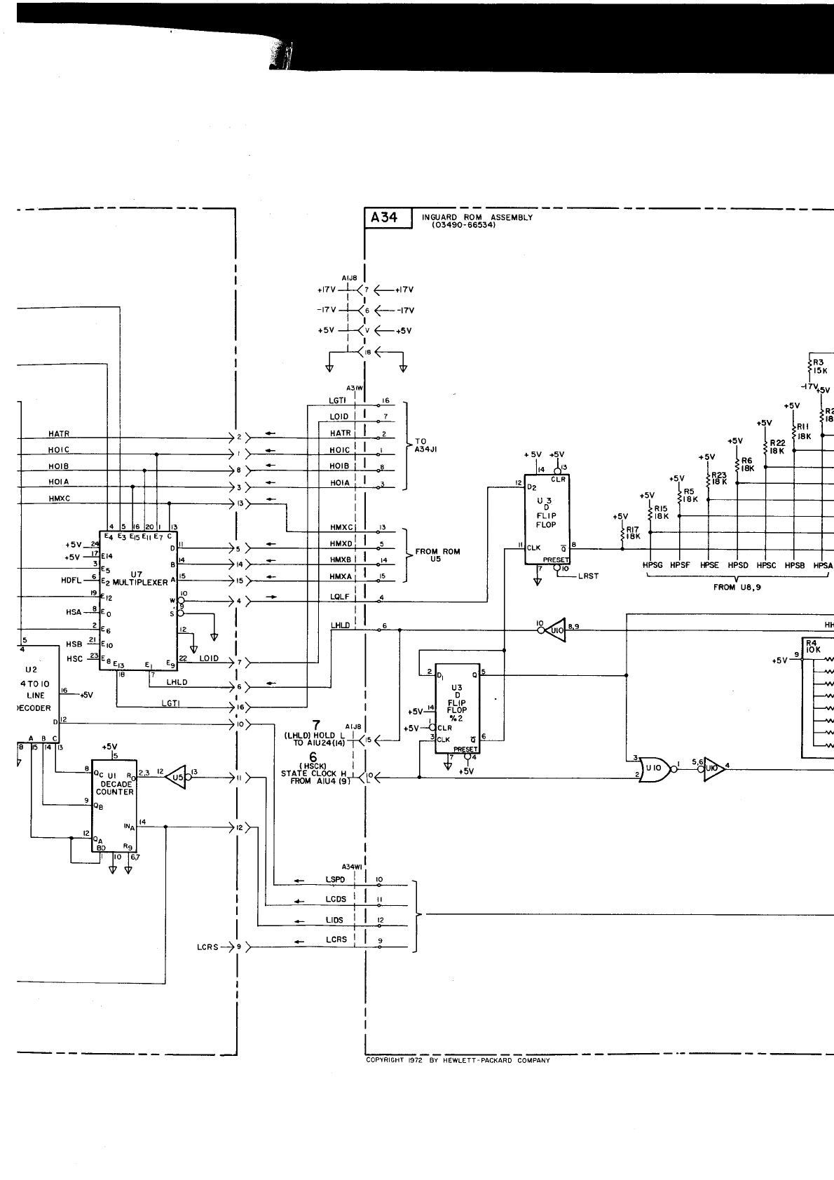
F^%ä!sJ.o!$"u"'
I
o,ra
I
',tuf,r 3+r7v
-tzv--L{e f -rzv
.uu
i-<," f +sv
T--<"e-l
ütü
:'l
'l
-l
- FIf",,
-l
I
r,)
l***"
F-
lrsK
7v+sv
}PSE HPSD
u7
MULTIPLEXER FROil U8,9
TO ROM
INPUTS
(U5)
@UNTER
A
FROM AIUI
V
[?,il9Bäloo'o*
20
TO INGUARD ^^
GPIS ISOLATION
4tJ
[ -!s]!r;. f .nn
| _tgts) ";_|_ r_oro
] HArR
>,o>'i- narn
I iqs)'>J- Horc
I rota
>z ;{- ro't
L_!ela)., >_l__
xora
iC HPSB HPSA
.*Jil
e
f rcrn
)-.1-+5v
I
I
I
I
I
ro
f xooo
I
I
;" \IJLEXE) ExrERtrlaL
i
,
I
TRIGGER ENABLE
L
," \L(LISH) INHIBIT
'- / SAMPLE/HOLD L
I
)!xooc
AIJS
>-l- HDoE
g
F-nooa
7
t8
__J13 )_l_r_soo
,-^st--)l ;-l--.r.t
+5V
HDCB
HIR8,
H IFA
R8
toK
HOCA
HIR A
| 0,,.
f
!E+;Fo'l
| "rne r ^. | ^ fnarce
/
| --------" /1-o)
,o J %:f szxuooe
18
" lff?"f:i''' u
| -----^ /-1-^l _...
I xrra
>r)j-u-ftutttroN
FR.M
a36
IiE],$nrucc1
üo'J
*u'>,for- lt
L HoPP
>
r >--r--eor-
J
+5v +5v +5V +5V
,o
l, us
,. READ
'' oNLY
MS,|ORY
702
19
Figure 7-37. Schematic
Diagram,
Inguard
program
and
ROM
Assy's,
A34, A36.
3490/O30-
E-32r7
1-1317-74
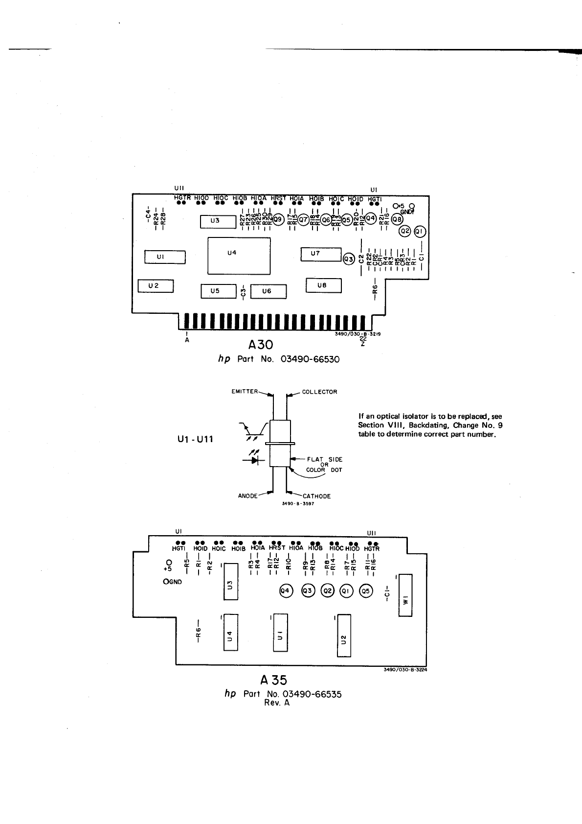
$i$
'EE
ll
tu'
_l
I ur-l
F@+p+F%o
ro'_ro*+++++++++{
llt"'
ul
-u11
430
hp Port No. 03490-66530
Port
No.03490-66535
Rev. A
lf an optical isolator is
to be
replaced,
see
Section Vlll, Backdating,
Change
No. 9
table
to determine
correct part number.
CATHOOE
;3f?
'S?o
'ti. 'lä?
fr?o
x?E
'i6q *1Ee
fi'&
x?ot
'tr'n
.?
+++lr++
++
+++
++ ++ ++
ocND [:J @ @@@
@ +
435
hp
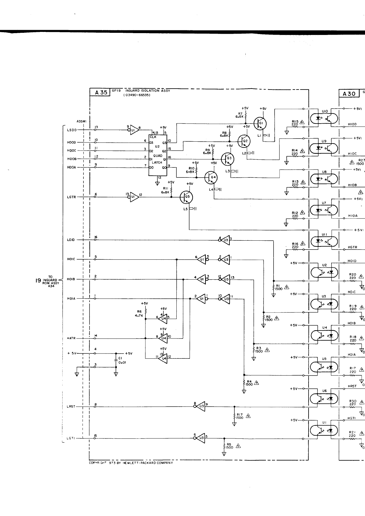
| ^ "ETGpr I -rl?ul'F5-ß-olqrroil
Ä's--
(
03490-66535, I
rl
rt
t *uu +sv
i ..r'-l ^l I I
+5V
R8
6.8K
nrz
A
+5V
4.7K R2 ,A.
tsoo 6
Rl7 ^\
+
R9
6.8K
A
+5V
I
+5V
H IOA
+5vr
HGTR
ä33
a
::: ^\
I
COPYR,GI'
973 8Y i€WLETT-PACXARD
COMPANY
R5,A
t500 a
R2r Ä\
zzo o
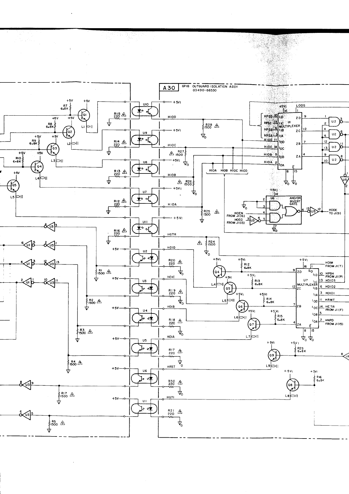
Rl3 Ä\
220 4
H toc
A '$'"'
+5Vl
H
IOA
!ä3
a
RI9
A
22O a
Rr8
a
220 4
Rr7 /d
220 ö
HRsr o
R28 /A,
1500 B
R25 Ä\
tsoo "HODE
TO
Jt(9)HOEN
FROM
JI
(16)
t-oEo
FROM
JI(I3)
lre
A
,gL
A
HOIM
FROM JI
(T
)
HPSH
FRO M
JI
(P)
t3
Rt4
6.8X
HD IO2
3 HO|O
I
II HRMT
HE TR
rROM JI (F)
Hr.lP0
FROM
JI
(I5)
R3O,6.
RI7 A
t500 i3
R5A.
l5OO a
R2r Ä.
220 4
|?
9
L0to2
LDIOI
TO OUTGUARO
MOTHER EOARD 4Z
I
fllff^",'Jg*"
I .o or.nroro
f orrl assv
?l
2 lnnF
+iö-ritsr
'
3 -:r03
=1., J1
(F)
z -..ri
r::M
Jr 05)
_-?'u
:iaM
Jr(T)
,: *xN
_ ECM JI(P)
+
svi
c2
39OO
pF
R23 2l
LR
FO
7
t7
+ 5Vl +5V
I
.l
+ttTk I
r fbÄiÄÄ;;;"-
" 2|
)-i xaor
J
I
I
I
\! !c,o FROM
oUTGUARo
- HL
rR üöllin" eölÄo" 2?
I
)--L xoeru
-l
( l .^,., l-rnou q:ra;ano ,
2 | HotM
lnoü a-ssi- " 2 |
i>--1- HPSH J
+ LEOP FROM
OU-GUARD
I MOTHER
BOARO 11
RI
IX R2 R3
6.4
K
K
HETR
I
HOEN
\
HOtM
i
I.,PSH.
---.-:-7
E5 A B C O
E7
Ez u4
g1 MULTIPLEXER
EO
E4 W
Etz
Erl
E9
tr^
zv
Figure
7-38. Schematic
Diagram,
GPIB Isolation
Assemblies,
A30. A35.
7-7517-76
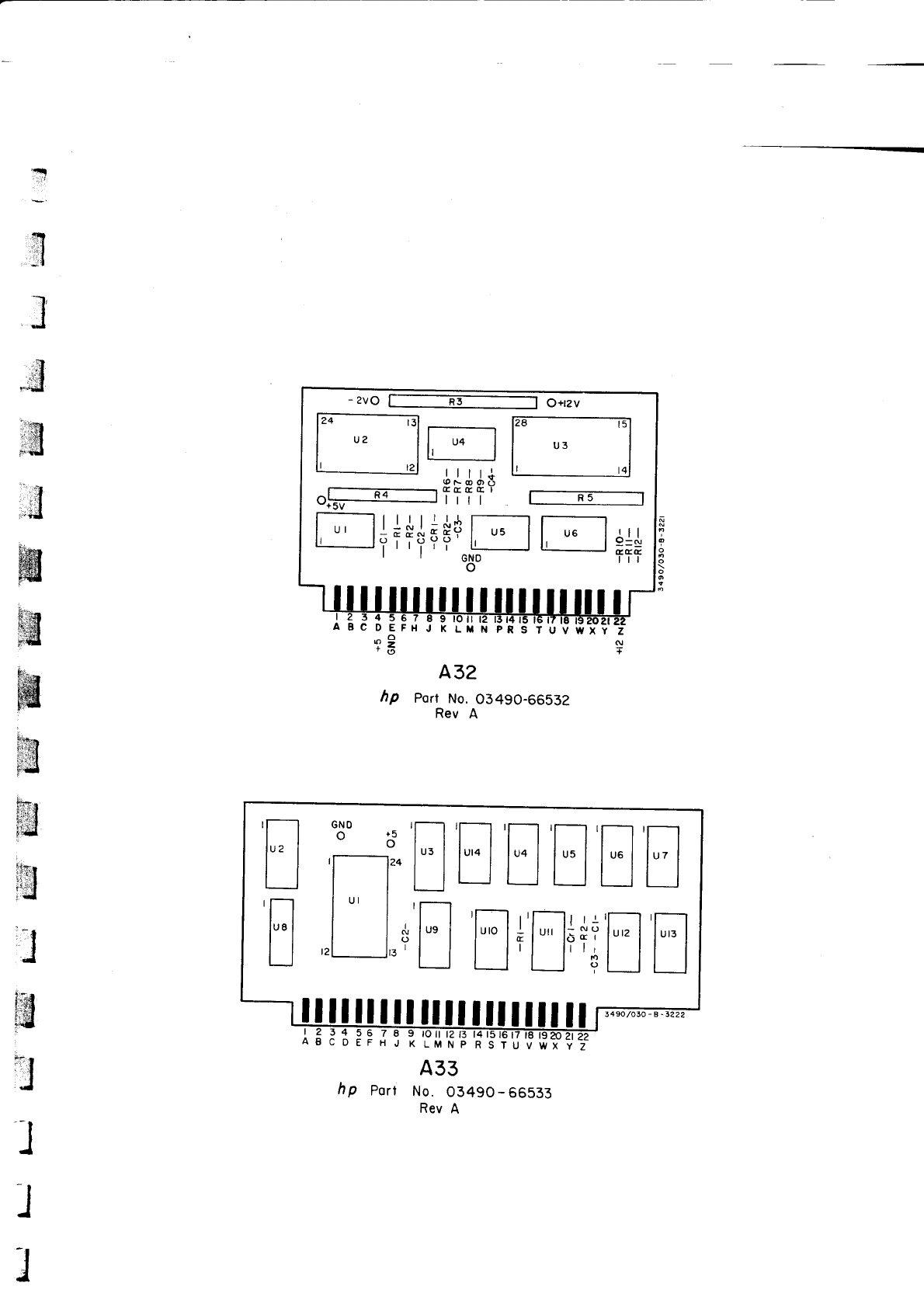
l
t
1l
ll
I
-ä
ffi
ffi
@
;3
'Tl
iäl
i'
:l
i
3
l
J
l
432
hp porr
No.
03490-66532
Rev
A
No.
03490-66533
Rev
A
- zvo l--------r-s-l O+rzv
l-ll
|"llu4llu3|
l' 'zl r_".
J
t
- z PEr-l -
o.!----l3_-_Jr]It I Ri------l
| | | t_L^r.s
l-------l
l,
'' l+Tt+FFtl
" ll " lij{
| | oöo -fTT
t4
r.l
LJ
n
lue I
LJ
ililtf ililtf ill
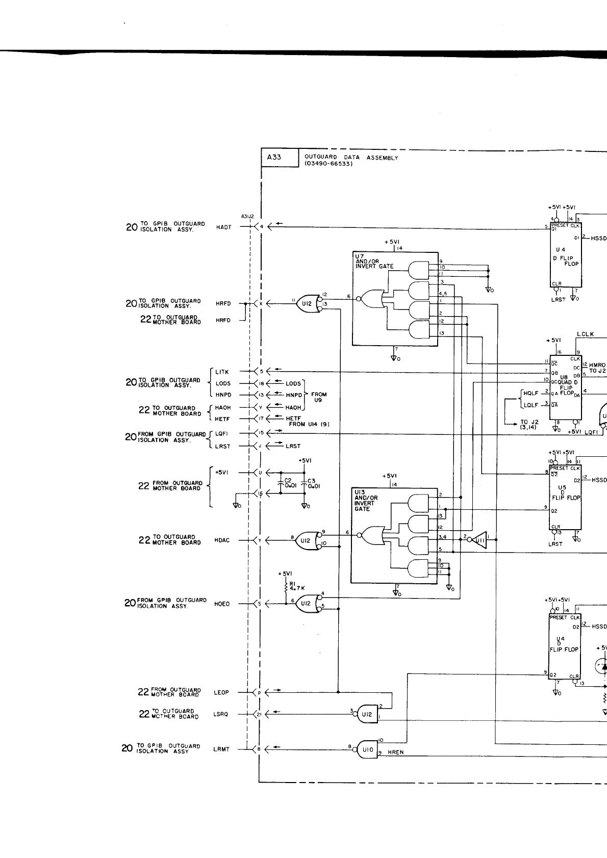
ASSEMELY
Ö^ TO GPIB OUTGUARD
ZU rsor-ÄrröH
-Ässi. - HAor
r.1TO GPIB OUTGUARD
4vtsoLATtoN AssY.
''TO OUIGUARO
LG MOTI.I€R EOARO
HRFD
1X
ti
HRFD J I
I lrrx
20A%ll?i8*o1lg9lRo
J r-oos
L xrpo
'' TO OTJTGUARD T HAOH
Lc MoTHER
roo*o 1 "aTF
66FROM GPIB OUTGUARD
f LQF|
cv tsoLATloN assy. 1L LRST
HMRO
TO
J2
ao TO OUTGUARO
<. MoTHER BoARD
20 t'SoJl.PJtit
^|5'IGUARo
roEo
22
i,19{#E8'^ffi0
LEoP
22
fr,.#|.!äi$o LsRe
20 loo.tflil"oX!3Voto
LRMr
--l-(v
il
il
il
--T'\.
it
il
ll
it
-rJ
ir
--1-<;,
il
{l
+
5vl
RI
4.7 K
+5Vi.5Vl
+5\
I
a-T
('4
Y
I
i('<--=
---L{rs(-: r-oosl
-.4{,. <-- xreo
I rnou
-l<v <-- HAoHJ
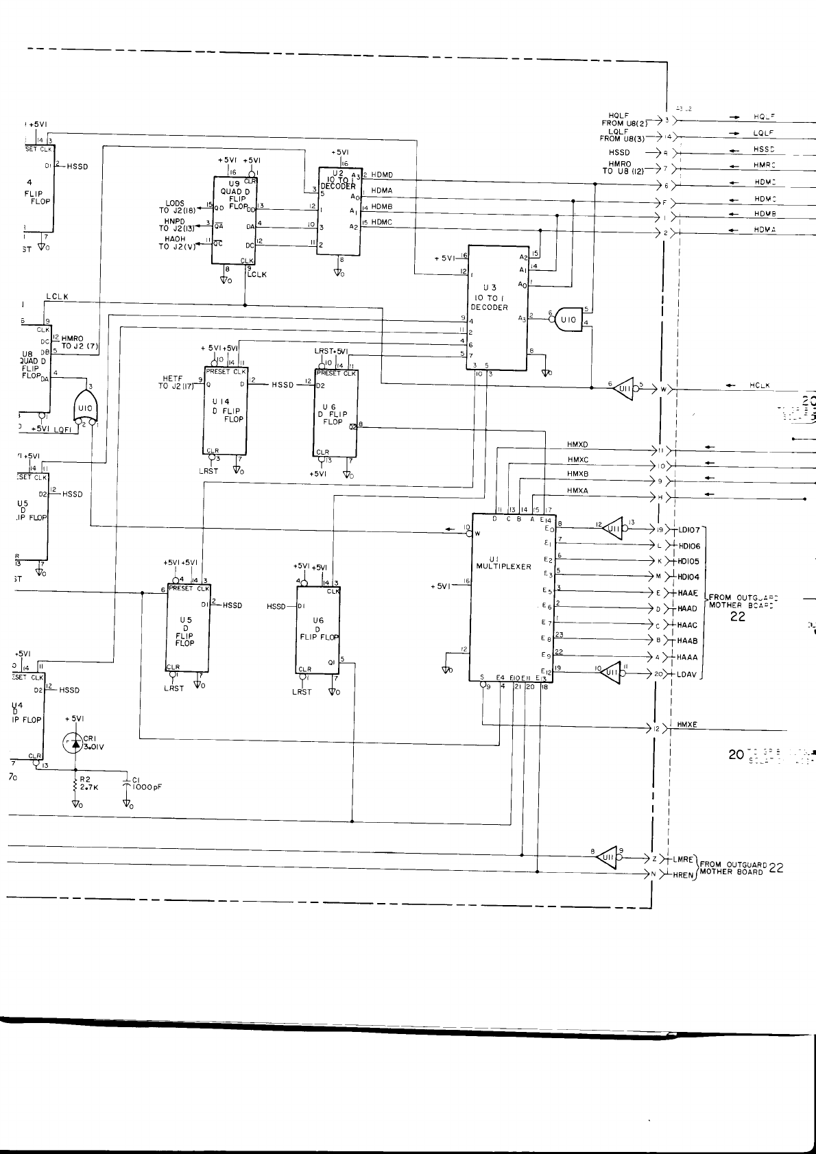
z z
.ggx3!.3'
i'ä.,!
{fi :
{ )
!8fx3td tltnw
zt ln
r3
"rl v I f, 0
'do']l o
d t'tJ
0 0vn0
n 60
oa
I
roooor
J
t3
-r za
3XhlH
I
\ -
I
I
I
I
Izz
l:Y38 U3HIOIJ
:3:^91nO r,tOUl
nvor
(oz
ooorf o
evvn{ s
cvvHl<
c
ovwf o
rvvH+<
r
oo'orf
^
n:*]1'
sotoxj{ r
c ---
^)
:AcH
+_.a_(€)8n r"loul
:rOr itÖ-t--
0
ssH
""do-tl
dnJ
0 ovnt
oa 80
lo
ttf,
--< (z)8nnou-l
z-:;
I
I
I
I
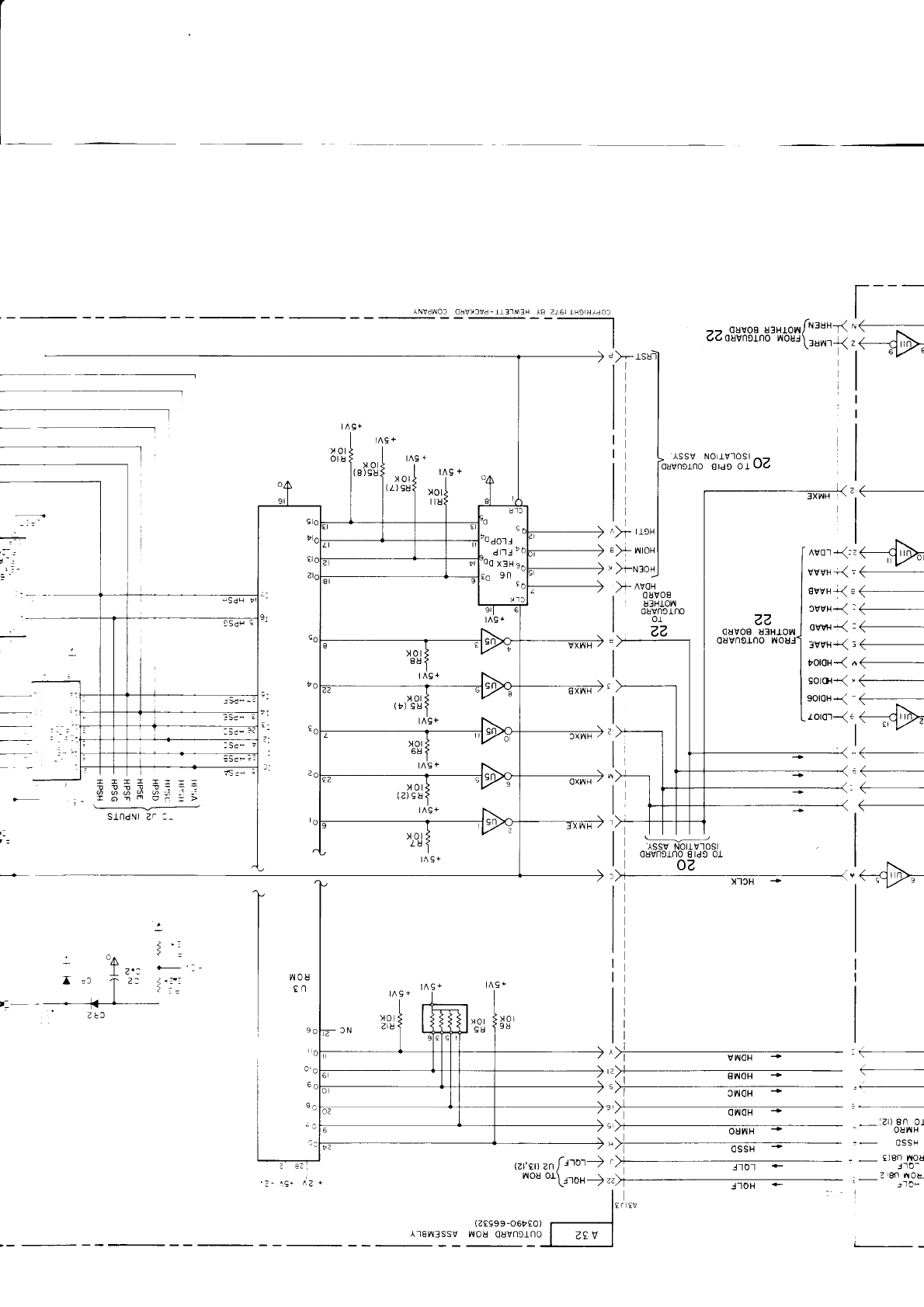
c8v)3vd-1r3lM:H ^8 2Z6l lHgrUldOl t---
-, ouvos ,rr.,-onltt"l1 t
<,6ouvn9rno noul\;uvlrJ<
r,
s
a
\- rqxi
/ : ---
^)r Ll,cH
sX nros
, lssv Nollvtost ^?
o8vnt-Lno €td9 0l vo
Fru:ox
>- ^voH
' 08vo8
u3H10n
08vn9rno
or
zz zz
08vos u3H10w
08vn0Lno
iloul
€vvH< e
(--
cvvH<
r<--
ovvH<
: <--
fvvH+<; <-
toloH-< ^ (--
90lot{: (--
sotoH-<
-
(- -
roro-r-(:,@
<-
<__
e-
<-
lssv Nottvt0sl
08vn9rno
€rdg
0r
oz
]>--
-
.-lzl)€n or
'/ ossH - - g)gn
lou
/ l1O1 l-t3-
zr8ft
ftor:
l. : - :-.lCs
t'
lr:v
(zss9
9
-o6t90)
^r8!,llssv no8 ouvne.rnoj_ll :J
\_
'/ onoH
\--
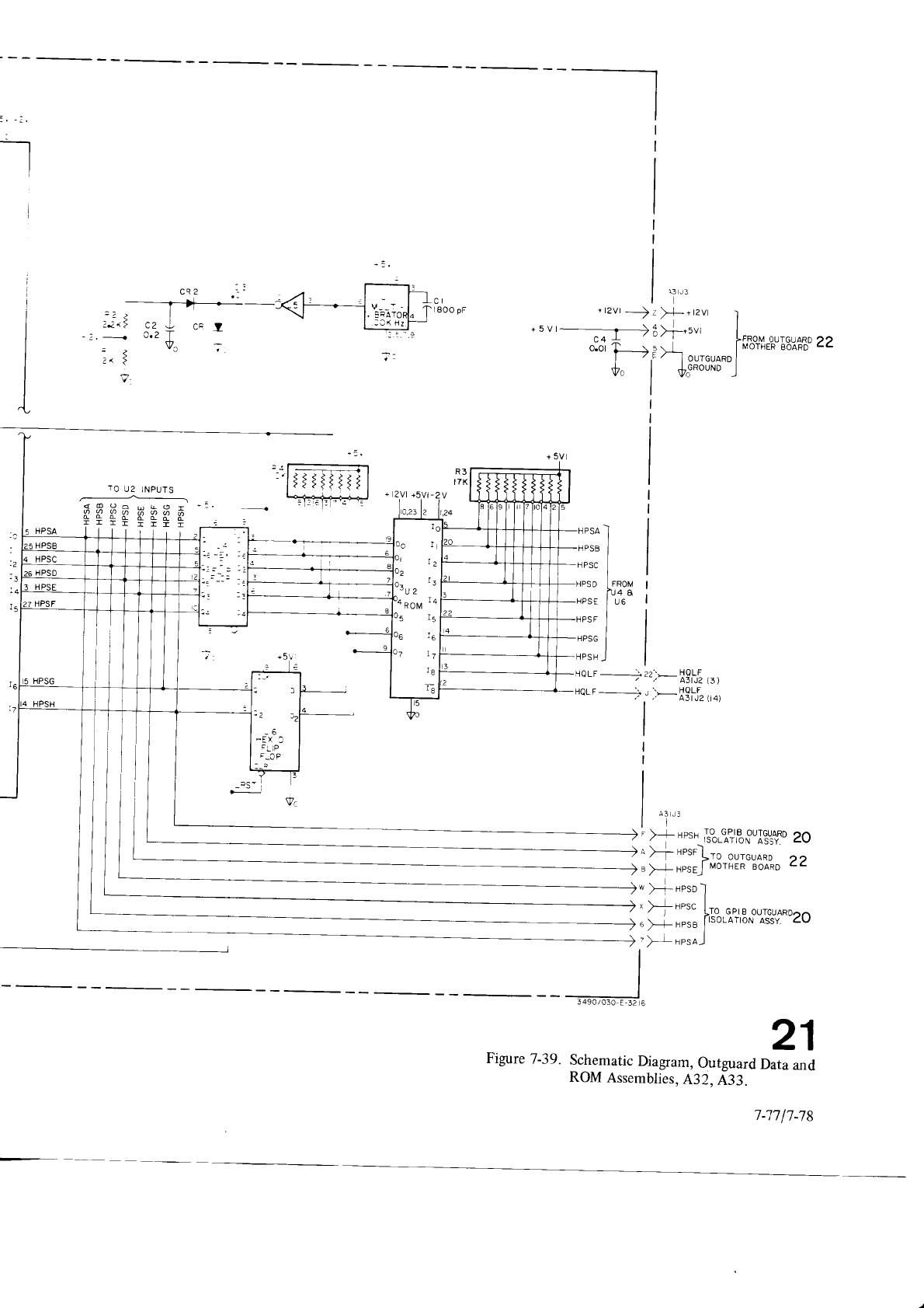
8L-LI
LL-L
.
tty, Zty .selquressy
1,qgg
pup
etr?C
pren31n6
,urur8erq
rrtr?uoqcs
.6E_1
ern8rg
l7
>v
TvsdH --< I
t^^
oz.,J,irYJg
il'r-%"]
::': - "
I
J>dF----\ '
I osar
-i{ ,
- - odvos ,rr-,0^ l-tao"
-\ "
6O c8vn9-rno
or5 .^.. i
1
'so"
-{ v
OZ
.Ä..31.J?il!.oosl-',sa"
]1-..,
,,
lo I
I
I
('r)
zf r€v_,. .
(e
) Zf lgv
_azz
(-- rroH
i_ t.röH
r HsdH
I
I esdH-
i rsdH.
9n I :SdH.
€rru
r/'{our
] asdH.
] lsdH_
I esar-r-
I
L
vsdH- #m+äüü*ü
\_____________v=
SJ-ndNl
Zn Or
I c^norff
I
08vne1n0
L_/
ZZ.9'"I3?'ü'?'591]
;
I r^E+_i1
L rnzr*_(
ea
t\
j
E
0
,x
5:
+':_ -
5;:
I
I:
3 ,nzr
*
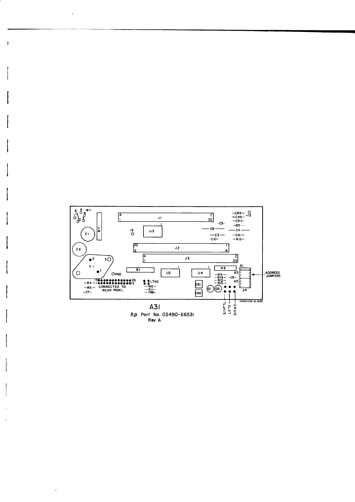
5 Wtl
)4
,f
o
6!
'1.
oo
I
L]
,Jl
-c8 -
-c3 -
-co-
-cR3- o
-cR5- '''
-CR4-
-R3 -"
-c4-
-c6-
-R13-
E
tT----l f--.-f ä=
| " I I'o |
:plr:
*i'l;il*
@
t -A;.:'li il
@ -o:'il 14
3:LrKo
- Rlo-
-Rll-
-cR6-
J2
J3
AOORESS
JUMPERS
J I | 549O/O3O-B-re
A3I FF?
hp Port
No. oi49o-6653t ; : .<
Rev A
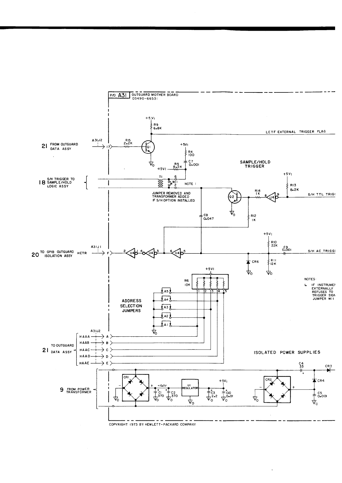
^Nvdr/'tof,
ouvvcvd-Il3"lr\3H
^€ €16t r
I
I
0^
to.o4P
orq*
-i-
.l
rAq+
^9?'+ +
o
z.z I ,,^,0,."o,,
^
|
""* wou' b
tz
€-r- rvvr-l
(--+-ovvx I
+lvvH F ^ssv vrvo
, I louvn9rnool
5--1-'oo' '
(r---r- vvvH J
0
s
v
s€
,)
s3t-rddns
u3/v\0d 03rv-losl
I
l/r U3dY{nf
\9rs u399r8f
ot, sfsnJ3u
^'rrvNU3.l_x3
J3Wn81SNt lr I
,s3roN
t99rur )v H/s
)9rul-
-111
H/S
9Vll u:l99luI 1VNU31X3 lI3'l
o3-'l.tv.t
sNt No[do H/s ll
O30OV U3WUOJSNVUI
oNV 03AOI{3U
USdtlnf
I 2.8
9U
r8.9
68
^ssv Notlv'lost t\2
UI3l{ Ouvngam
gtao Ot
-.
^ssv 3t90'l
oroxz:ranvs
$ |
or u399lul H/s
^ssv vlvo ._
ouvngrno wou.l I d
eI
tf r9v
l
roo.o
L)
ool
bU
>42.2
9lu
lA
9+
I
r€sss-06r'0
-l
ouvo€ urHrov{
ouvnsrno
I IEV ora
I
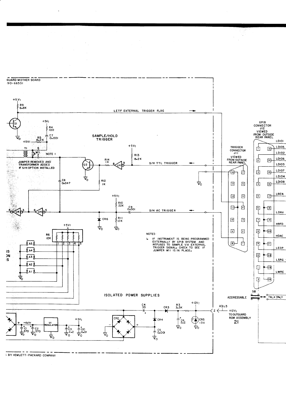
GUARO MOTHER BOARD
.9
0- 6553
|
4iaa:'
,:1 '
:.1t..:.
SAMPLE/HOLD
TR IGGER
G PIB
CONNECTOR
VIEWED
FROM OUTSIDE
REAR PANEL
LETF EXTERNAL TRIGGER
FLAG
+
5Vr
S/H
TTL TRIGGER
TRIGGER
CONNECTOR
Jtl
VIEWED
ä' NOrE I
JUMPER
REMOVED ANO
TRANSFORMER ADDEO
IF
S/H OPTION
INSTALLED
FROM
OUTSIDE
REAR
PANEL
AqtJ3
z (-i-- +rzv1
TO OUTGUARO
ROM ASSEMELY
2l
s8,
-
A0DRESSABLE
--*-rAi'-xo4LY
NOTES'
L IF INSTRUMENT IS BEING PROGRAMMED
EXTERNALLY
RY GPIB
SYSTEM ANO
REFUSES
TO SAMPLE VIA EXTERNAL
TRIGGER
SIGNAL. CHECK TO SEE IF
JUMPER WI I IS IN PLACE.
ISOLATED PO$/ER
SUPPLIES
+lzvl
+5Vl
tr
a
TN
ü
tr
S/H
AC
TRIGGER
I AY HEWLETT-PACKARD
COMPANY
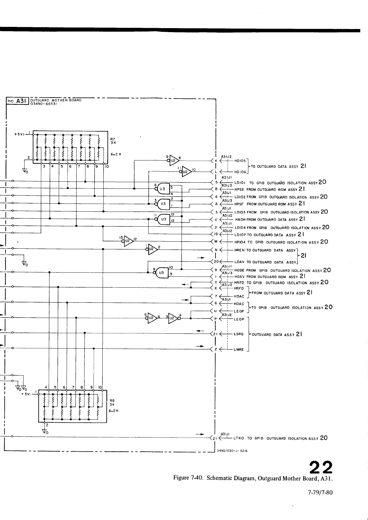
08-Ll6L-L
'I'V
zreqlot{
pr?n8lno
'rue€e1q
crleruoqcs
'671 arn8rg
'prBog
z
l'
l'
srze-r-oeozosre
f
OZ ^ssv
Nou.vlost
0uvn91no stdg
or Ortr
ffi
oz^ssv No'v"losr
ouvnerno
.,.0 o.,.{ :ott-- n
l_
cvon-j) e
r ,oo, ''''to)
a
lZ ^ssv
vtv0
ouvncrno
norr{ orrrf ,
OZ ^ssv
Norrv'rosr
ouvnerno erac
or orur ztisv>
^
lZ lssv wOU
ouvn9rno
nouJ
AvoH-+.J I
OZ^ssv Nou.vrosr
ouvngrno
srdg
y{our
rooHI--} e
f^ssv vLvo ouvngrno
or nvor_Joz
E4 i I
lrssv vrvo ouvngtno 01 N3uH-1) N
OZ ^ssv
Nolfvlosl ouvn9].no
stdg or rotdH-+J n
I Z ^ssv vrvo
ouvnerno or r.oror;jt' .,
oz ^ssv
Norrv"rost
ouvn9rno
stdg
WouJ roto'l
--r_) z
lZ ^ssv
vtvo OuvngJ'no
y{OUlHOVH
:-l- ) A
oz ^ssv
Norw"losr
ouvngrno srdg ^ou*o,o-, zfp! n
I
Z ^ssv $rou ouvnelno
wou.l JsdH
---J v
OZ ^ssv Notrviost
ouvn9lno
sldg l^loul zoto"l
-_-=) t
lZ lssv l,iou o8vn9lno
wosj 3sdH--r-t I
OZ^ssv Norrv"losr oqvnelno srde or rorol:-15 n
Inlev
I
IsoroH
-r-) r
lz ^ssv
vrvo
ouvncrno
orl i . I
LsoroH
_€ v
,42.9
8U
rss99
-06t€o
08vo8
u38ron 08vn9lno
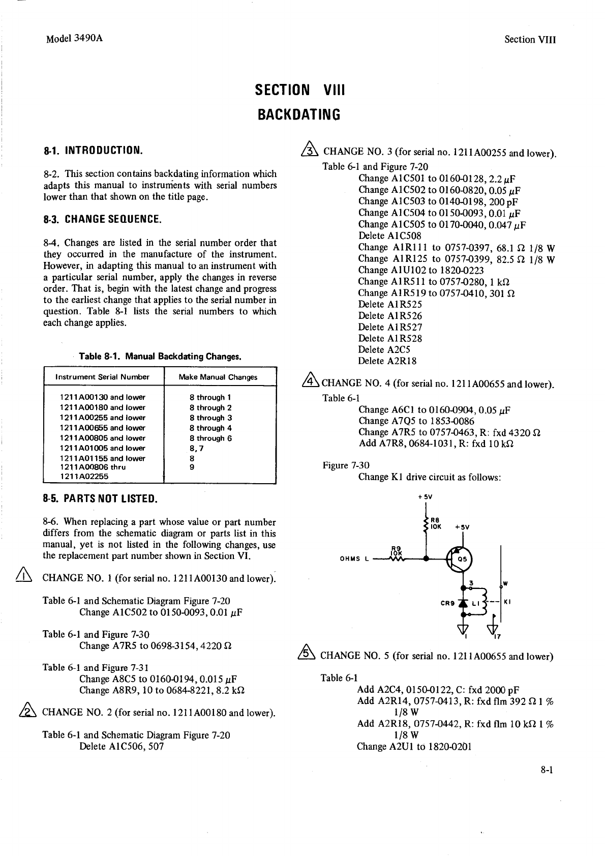
I-8
ob
%
I0zo0z8I
ol Inzv eSuBqJ
A\ 8/r
I ö)t
0I UIU
pxJ
id.'zttuLsLo
'8Iuzv ppv
^\ 8/I
|
ö z6€,
uru
pxJ
:u
'€ltürsro
'tldzv
gd
oooz
pxJ
:J'zztyosto'rJzy
'(rarnol
puB
SS900V
I IZ I .ou
puos
roy)
? .ON
ACNVHJ
\z
w
gluzv eleteo
sczv elelec
gzsuIV elole(I
lzsuIV elele(I
9ZSUIV
elolec
szsulv elolec
ö lgt'gItGLSLOot
6tSUIV
a8ueq3
ö>t I '08ZGtSt0
ol I I SUIV
a8uuq3
tZT,VOZgt
ol ZgIntV aEuuq3
^\ 8/t ö s'28'66ttLsr0 0t szlulv e8ueq3
A\
8/I ö t'99'L6€tLsr0 ol IIIuIv a8ueq3
80sJIV eleloc
Art LVO'
0,0ü00-0,
I0 01
SSSJIV
e8wq3
drt
I0'0't60O0SI0
ol tgSJIV aEueq3
dd 002
'g6I00tI0 ot
€SSCIV
etueq3
drt S0'0.028&09t0
01
Z6SJIV
eEueq3
Afl
Z'7,
'gZIG09I0
or
IgSf,IV
e8ueq3
g7-7
antugpue Ig olqul
'(relttot
pue
08I00VI IZI 'ou
pues
rog)
Z 'ON
ACNV"C V
ö{ Z'8'IZZB+99O
010I
'6U8V
e8ueq3
Crt
SI0'0't6Ig.09I0
ol SJ3V
e8uuq3
1g-1
arn81g
pue
I-9
elqel
ö OZZ7' tStE.g69O
ol SUrV
e8ueq3
69-1
ernErg
pue
I-9 elqel
dr, I0'0't60G0SI0
ol
Z6SCIV
a8ueq3
g7-2
antug uer8urq
clt?tueqrs
pue I-9 alqel
'(ramo1
pue
0tI00VI IZI 'ou
pues
ro3)
I 'ON
ACNVHC
'J^ uoqces
ur uÄ\oqs
requnu
ped lueureceldar
aq1
esn'so8ueqc
Eurarollo;
eql q poFII
lou sr
lef 'pnuuru
sHl ul 1sq
slred ro tue.6erp
c4?ruoqcs eql uorJ sroJJIp
Joqunu
ped ro enIB^ esoq
\ pud e Surculdar uaqr11
'9-g
'orlsr]
roN
sruvd
'g-8
'sarldde
aEueqc
qcue
qrII \ ol sroqunu PrJes
eql slsl I-8 alqu; 'uorlsonb
w requnu ppes eql o1 segdde
1eq1
eSueqc
lserlreo
eql 01
so.6ord pue e8ueqc
Nolq eql qlpl ufoq 'sr lurl1, 'repro
esJe^eJ
ur sa8uuqc
aq1 Ä1dde'raqurnu
pges rulnclped e
qll \ lueunJtrsrn
uB 01 lBnu?Iu
srql Su4depe ur 'JeÄe/noH
'lueturulsut eql Jo ornlcuJnrr?u 3q1 q pauncco Äaq1
leql JapJo requnu Fuos eql u pals[ are satueq3 f7g
'33Nln0ls
l0Nvl{3
't'8
'eEed
apq eql uo u^\or{s
luql rnql re^\ol
sleql'unu prres {1l,rrr
sluerunllslrl ol IBnII?tu
slq1 sldepe
qcrq/h
uoqeruro;ut Eurlepqc?q
suptruoc uorlres sr-ql 'Z-8
'N0rrcn00urNl
'l{
,0s.g09JIV
elelec
g7-1
arnErg uur8erq
cq?ruoqcs
prrB
I-9 olqel
ppY
ppv
I-9
sIqBI
(ro^/r\ol
pu?
SS900VI
IZI 'ou puas
rog)
S
'ON
SCNV", V
'l snHo
:s^\olloJ s?
lrncJrc
e^rJp
IX a8wq3
gg-1
ernSrg
ö{ 0I pxJ
:u'I€0I-t890'8UtV ppv
?J OZE7
pxJ
:U';q7O-LSLO
ol SU4V
e8ueq3
980GtS8I
ol SötV a8ueq3
Crt
S0'0't06O09I0
01
IJgV e8ueq3
I-9 etqsJ,
tx
lvt
'(ramol
prrp
SSZg6VI
t1t.ou prras
roy)
E
.ON
1ICNVHJ
\f/
V
cNrrvo)tcv8
iltA N0trSls
6
I
L,8
9 q6norqr g
t q6norqr g
e qonorqr
I
Z
qbnorqr
g
I qonorqr g
ggZZOVLtZL
nrqr
go8oOV
I lZ I
JeMol
pue
99
t lov I tz I
rsMol
pue900lovltzl
raMot
pue90800vltzl
rai ot pue
9990ov I lz I
ra,ttol
pue ggzoovLLaJ
JaMol
pue
08 toov I tz I
.bMol
PUe
0e
toov I lz I
se6ueq3
lenuen
a{eW raqulnN
leuas
lueunrlsul
'sabueq3
6u;up>peg
pnueu\l
'!-g olqel
IJIA
uortros v06t€
lepon
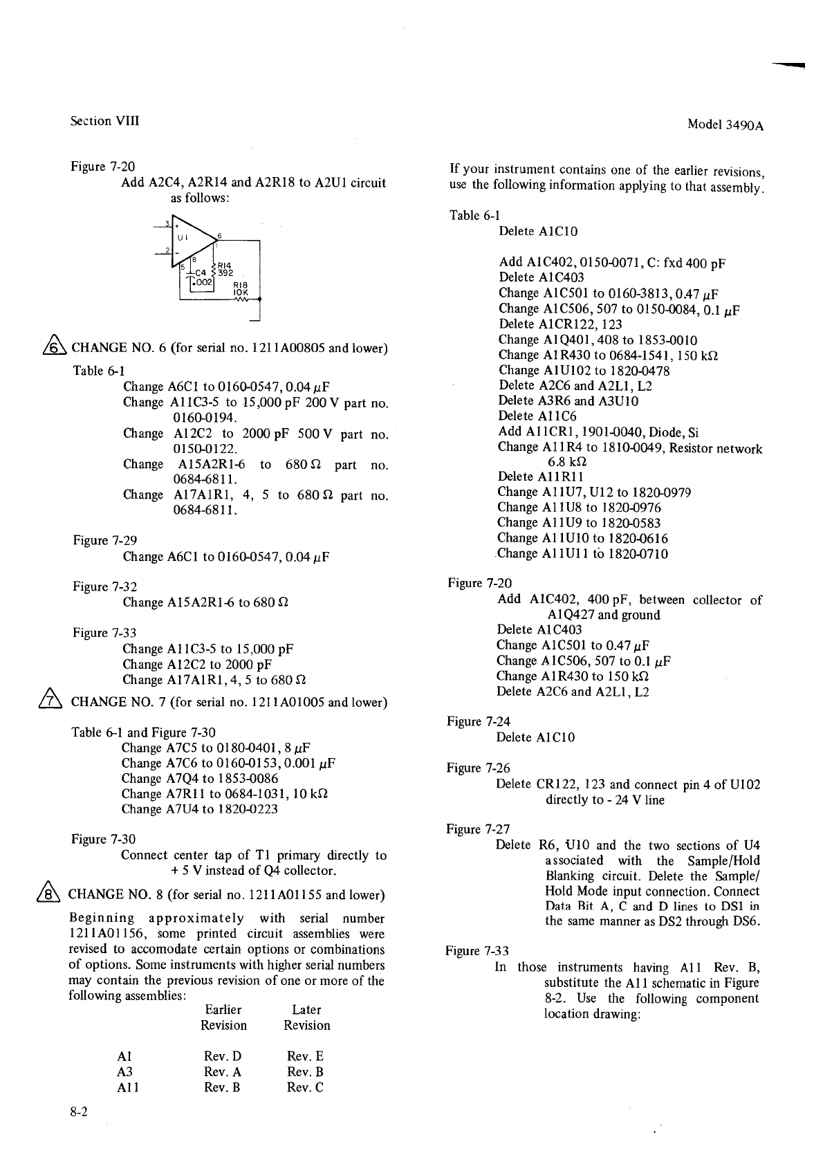
z-8
J'^eu
g'^eu
a'^eu
g'^0u
v'^0u
c'^0u
IIV
TV
IV
:3ur/rwrp
uorlecol
luouodruoJ Suurrollog eql esn 'Z-8
aJngrd
ur
crleuaqcs
I IV oql olnlr5qns
'g 'rrag 11y Sqluq sluerunJlsrn
esoql uJ
gg-1
arn8rg
'9gq qSnorql ZSG
se reuu?ru
orues or{1
ul ISC 01 soull
Q puE
J'Y llg etec
lseuuoJ'uollceuuoc
lndur apo4 p1o11
/oldurug oqt aleloq 'lrncrrc Euquelg
p1o11i elduug er{l q}1lrr pelercosse
?n Jo suorlsos o/ht or{l pu? OIn 3gu ololec
77-2 antug
eu11.p
LrZ - o1 Äpcarp
Z0In Jo
7 urd
lceuuoc
pue
tZI '771X3 eieyeq
97-7 emtug
0IJIV elaloC
p7-7 atntug
z-t't-tzY
pu?
gJzv elolec
15l{ 0SI ol gttgly a8ueq3
Crt
I'0
ol
r0S'90SCIV
e8ueq3
gA
Ln'O
01
ISSJIV
e8ueq3
e0tJIV elolec
puno$
pve
LZTOIy
Jo rolcelloc
ueoaleq
'Cd
00t 'Z1t)Iv
ernBrg
0lr00zgl ql I InI Iv oSwqJ
gtg911gt
ol
gInI1y e8uuq3
t8S0{Z8I
ol
6nt
1y a8ueq3
9L6V0Zgt
ol 8nI1y e8uuq3
6L6OAZU
ot
ZIn 'rnl IV a8ueq3
IIdIIV alelac
ö{ 8'9
{ro^\leu
rotsrseg'6t0g"0lgl
ot
tUI1y eEueq3
IS
.EPOIC
.0'0}106I .
IUJI IV PPV
gJl Iv etol3(I
0Intv puB
guEV
alolec
TI,tlZV pu? gJzV
elelec
SLV9OZB1
01
Z0IntV e8ueq3
i5>t 0SI'I?SI-t890
ot
g€tgIV e8uuq3
0I0üES8I
or
80t.'I0t01y a8ueq3
tzI'zzIEJtv elotoQ
cr,
I'0't80o0sI0
ol
rOs'90sJIV
a8ueq3
Jtt
L7-1,tlgt-ggI0
01
IggJIV e8ueq3
€OtJIV olelac
cd oo?
pxJ
:c'ItoGoslo'zotJly ppv
0IJIY elelec
I.9 OIq?J
'Älquresse
leql
01 3urÄ1ddu
uorl?uuoJur
Burno11o3 eql
osn
'suorst,rar
rarlJ?e
oql
Jo
ouo
sureluoo
luerunJlsur
rnoÄ g1
Y06tt lopow
uorshau uorsr ed
J€}e'I rerlJsg :
sellqtuess? 3urrto11o3
er{l
Jo ?Jorrr
Jo ouo
Jo uorsr^eJ
snorlerd eq1 ureluoc Äuur
sJoqunu
puas req8rq
q1p\
sluoturulsur
otuos
'suorldo
3o
suorl?urquoa
ro suorldo urepoc eleporuoccs
ol pasr
oJ
ore r sollqtuassu
lrncJrJ pelurrd eruos '95I IOVIIT,I
Jeqrunu
IEIres WIn Älaleulxordde SuruurBeg
ppv
oz-L
(ranolpue
SSIIgVIIZI'ou
prres
ro3)
8'ON
1ICNV"J
Y
'roloolloc
t0 Jo
p8olsul
A S
+
o1 ,(11cerrp ,fteurrd 11 1o d4 Joluoc
lJeuuoJ
gg-1
arn8rg
;ZZUOZBy
ot tnrv a8ueq3
ö{ 0I 'It0I-t890 ot I IUI,V
e8uuq3
980&tS8I
ol
t}rv e8ueq3
drt 100'0'€S I009I0 ot
g)Ly e8ueq3
Cr/
8
'Igt6-ggI0
ot
g31y
e8ueq3
gg-1
ern8rg
pue
I-9
alqel
(rainoy
pue
S00I0VI IZI 'ou
puas ro3)
, 'ON
ACNV", V
ö 089
or
S't'IUIVTIy e8uzq3
Cd
0002
ot ZJT1y
a8ueq3
dd
000'SI
ot S-tJI1y eEueq3
Eg-1
arn8rg
ö 089
ol gtUZVgIy eEuuq3
79-2
erßrg
drt t0'0
'rtsg{gl0 ot IJgV e8uuq3
67-7entug
'I r
89-1890
'ou lred
ö0g9 ot S 't 'IUIV11y a8uuq3
'I
I89t890
'ou ped ö 089 ol g-IUZVSIV e8uuq3
'zzlo{sro
'ou lrud A 00S dd
0002 ol ZJT.lv aEuuq3
't6I0{9t0
'ou
ped
^ 002
dd
000'SI
or S-gJI
1y eEueq3
Cd
t0'0'LrSy-,OglO
ol IJgV
eEuuq3
I9 EIqBI
(renolpue
S0800VIIZI'ou
puas
ro;)
9'ON ACNV", V
:s^\olloJ
s8
lrncrrc
Inzv ot
gluzv pue
tluzv'tJzv ppv
g7-y atr€rg
IIIA uoures
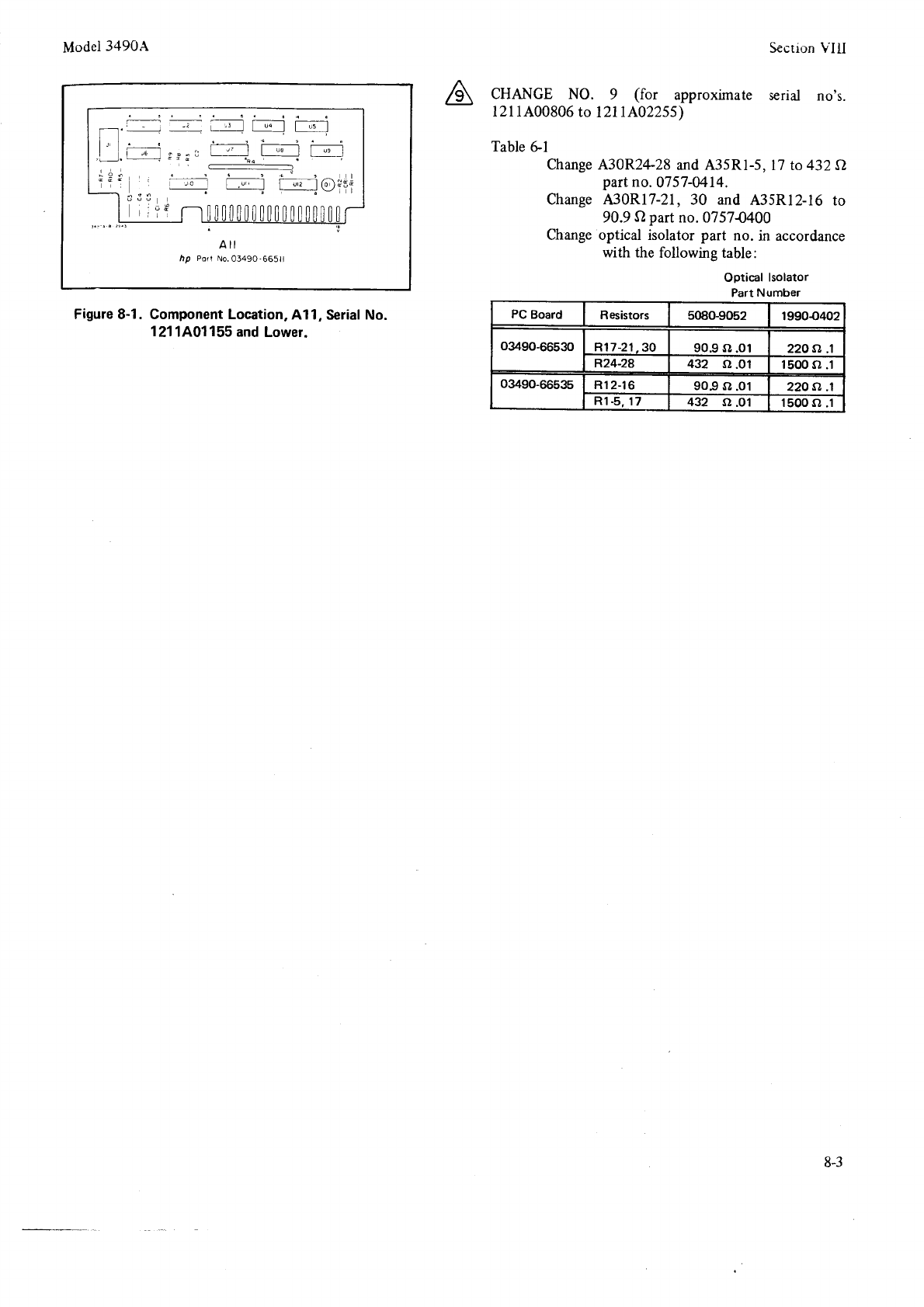
t-8
t'
rJ
0091 l0'ö ztn Lr'9-tu 9e999-o6180
t'öozz t0'ü 6'06 9t-zru
I u 0091 t0'ü ztv 8Z-VZE 0t999-o6t€o
L'öOZZ 10'ö 6'06 0e-tz-zlu
z0r(>066t 2906-0809 srols!seu preo8
3d
ßquJnN lred
rolelosl le3lrdo
:elq4 SrrA\olloJ ärI1
qtl^\
ecuBpJoccs
urou u?d rolBlosr prrldo eSwqJ
}}VhLSLO 'ou il?d U 6'06
ol gl-zlus€v pu?
0E 'Iz-llu0tv oEwqJ
'nlvo-LsLo 'ou
lIsd
?JZtror
rI's-tus€v
puB
Sz-'zu0tv
eSueqJ
I9 EIqsJ
Gszzov
tlz I
01
9o8oov trzl
's6ou lelres aleunxordde roJ) 6 .ON :ICNVHJ
JII^ uorl3as
'r0,l
o'l pue
ggllovllz!
'oN
leyas
'tr
1y 'uorleco-l
tuauodruoC
'
1-g
arnbr3
ltg99-o6'eo oN
riod dv
ilv
v06t€ lepow
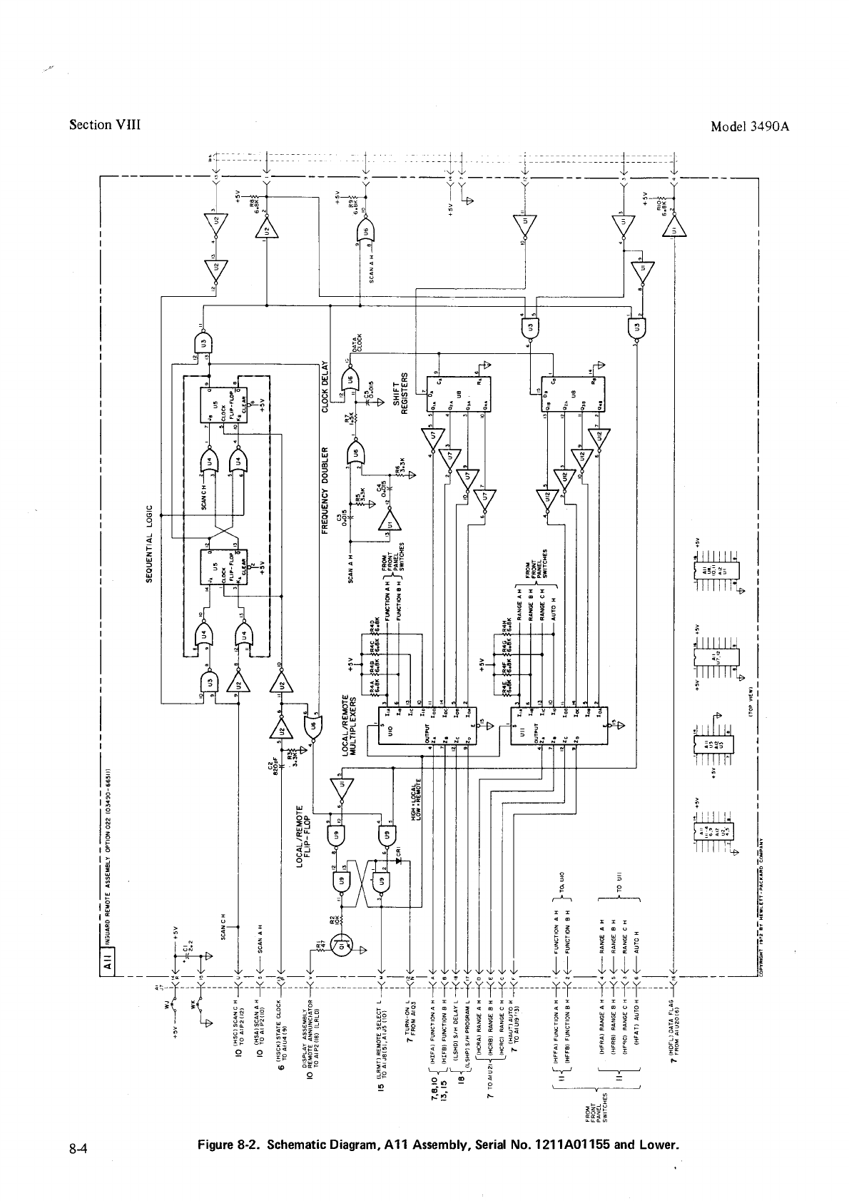
'.|a^
o'l
pue
gglLoV![Z!'oN pl.res'^lquassv
LLV'rueroerg
clpuaqcs
'7-g
arnorg 78
r
o
c
m
z
I
5
o
d
i
;-
II
-t
^
----i .I
i
::
_rt
92
3
Eää
i
Pi'
ä333
däää
{äää
iFi.
T\ 4\.4\ /]\ .1\
,n
tttttl
tttltl
iiää ii
z>
L_.."rJ \/
d9
III^ uorlces
YO6'E IEPOW
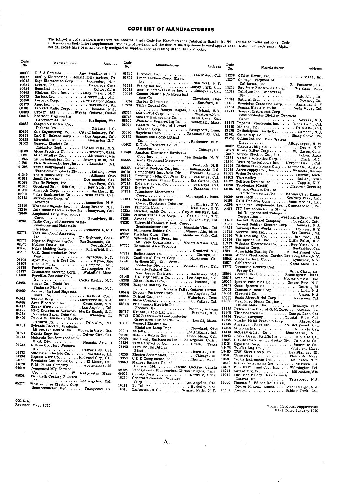
IV
0L6I ÄJ3nu"f pat"o I-tH
sluaualddns
{ooqpü"H :uoJd
'lEJ 'Irrd uröplrg . .. . .socuoJ 6896I
'f'N 'atu"Jo lsal\ . . uosrpg-a"JCcW
Jo.^rO
.salJlsnpul
uoslpa .V s"uoql 0096I
'fN'oJoqJalal .. ^rclorluoc
T uorl€5r^"Nr'dJoJ
xlpuag aql 9Ie6I
'srt\'aa{n"alrt^I .... .oJ.8JWlu"Jn( 1168I
'IaOruol.äulullA\
' . . .cr4 ,'oC pw luodn0 .I.S 0l,8BI
'"d 'uJa^I"!{ .cq sluaunJlsul,t"q"trf Ziggi
'Ä N'ocsrt 'ly,t'
' ' 'cul,lu"unrlsul
surn3 69981
'ss"II'?Ilt^ut"ld . . srrJauoqJ 9998I
'lII 'saur"ld
saq .. . . .^rC.duo3,loalg
11UJ g3tgl
'ssEr^I
'üolsrlloH .cul, .oJ.9I!I r"C-i(I glrgl
'IlJ'aIE^duunS .d:o3 scnauSrg 9ggg1
'I!J'olIV ol"d . .^lq rolanpuocruag,d:o3
altlatC CggSi
'I"J'olIv oled . . . . . .rül clIrc"d uarsaq
ranot z'08i
'H N'ralsaqcu€I.t
. .....ocuoslpg-ner9cl,{ [1811
'I"C'alB^,(uurS' . . .rul xruocrlrs 99grl
'I"J 'p@a,t1oH .oN . . . . .cq.caJd uqo:qs:uy gglli
orq6'.uorfy . . .' .droC
slcnpord IBloI,{
unuEH al,gti
'I!J 'aa!^ urElunor^l
. ,{u"duoC xauct; 91pli
'l"J'{r€d "5ouBJ . .cu1
srrlauouraql 6g1ji
'pq'ouoto)t.' . .dro3.!{'g Jo ^rqolpsu ocreq giigi
'Ä N 'uillooJg .^rq Jalalil Jnf aq
.cq, .oJ Jalol{.card IBapI 8899I
'I"J 'aap€s"d ' ' . . . ..droc lnN tJ"rcrlv stos agaöi
'f'N 'uotun .o3 p10r1ca1g
f99!1
'f N'!po.r ... .droJeporq:alnaud5 äöööi
'tII'rlorla(I .....rqrrlcadg-ruuo tiiii
.! ll lau16 arnrqs . . . . .oC ratn aurd "r-G jlööi
'IEJ 'aal^urquno!{ .. -cqorlauy glg€i
's-sli{_'_u-"_q3u!u"JJ
. . . . . .'aut .tcatg l"au_al lgg;t
'J"J'"J"lJ"luES .. ... .o3tutJds
_ IIoC,(rnluac qlanuaöI ?llgl
'I"C'"saIIstsoc... .. srluoJlalq"c
l89ql
'tr N 'rroorqul.I .droC .taul aqoräui 6öögi
'Ä N?uplsl äuo-I
.ÄltJ qap&cl .scluor1ce1g
uo"clrt s99li
'I"J.'pooMIIoH .N . . . . .oc aurqs"g
arqqsnfw iääii
'pc,asptnoroN ......drc1ia1ur!"Ä ;öäi
:1..-N.__rj:l 1"n' ' ' ' ' .oc srluoJlaars ralsqaät ;öiii
'f N '8IIEJ anl!.I . . .rul,.oC aJaqds
aqJ göi;i
'IEJ 'üof urg . . . .oC .jllt "rirq111; öö;;i
'l"J'lo_!rqEc
uls .' .' . .. .. ..auraqn3
oacalg ?grii
.1:t! :1!tt9J ' ' BrJoÄ ssqc Burur;5 ;;;;i
:i l_':!Ii?N ' ' droC crrlrats rarlqnq nauro3 ggiii
'oloJ,'Fü"IeÄo'I . . . . .ÄwduoJ prz{ce6_ila1naH 66Wl
'"IJ 'rlc€aq ul"d lael\. uolltJodJoJ
qdaltelo& Fr" äuoqdalal .lul
,o .^IO
E .Jolcnpuocruas
J,II ggrrl
'_"d'ualcoqoqsuoC. .'cul .
sluauoduo3
ucarrauy [6gp1'I?c'Erluo!^t
Eluas .'. .. .
üoC rolsrsag.llpa iiiii
'1tC
"l&dÄrnqaoN. .....qaa;_weg 6!6pl
sBsu?)t '.{lIC s"suz)l. . . Jq.saI4BtrE{ cIJlcBd
, to .^tO tqtui$_Frslpfll 908eI
^u€uJec'raÄou?H (Hquc) uennlara; ö6iii
_I.I '=lgtJ ' ciq saclaaq uo:1qo5 l,ise i
sqar 'sqtuq . .roirou:airJ iöiöi
'qcu^t'Iorloo .... stcnpordocltÄ
ii6;i
s?s-uyy'"I!qJl!^l
. .. .. .rul..oCi(tdd$ocrr.y il6ii
w@uv 'al?ps.llors . ..droJ scruoJlc€Ig
*"rl"rd ilöä;
'I"J 'r.trtag
uodaaN . . .cul rolrnpuoJtuas
qlaq oedii
..ll-'y:l? . .dro3 srruorrcars xalaa i[iii
y.T:{,_-.11"J'' . pr.l
..o-C
arJlrars
uoaalp
Oieäi
'woJ'ua^EH
^\ .........dJoJ^rallg r*It Stti'HN,ra^oo ......oJ.tJyllqsoed ;;9;;
'IJ'N'anbranbnqlv.... .....,..^Iq
- qatsÄS
"1"(I, .cul.FrI uollno ,[9ZI
::g'?^orcÄpcqs
...... .cq,.oJ.5ma^,;.ö iö;äi
.l-I. u:p-tc 'o3 arprng zrqaräpurrqä ööiäi
'IBC'ollvolEd .
... .. .rul,"q"r"lt öiöii'1zC ')tr"d wang . . . . .cuy,cuorlcalg lBrjadui ;ili;
'f N'IJ"aaN .l d.o"g
alcnpoJd uo!8t^KJ rolcnFrocluas
. .droC
luawnqsq IErauaC IIIII
'I"o '"san qsoc. . . . . .rul acluorlrala munq ,€ali
I N,'"c!"u"f . . . . .dro3 Jqlcewoc uorelcarg ggyii
'I"J'{auaoo. ..... Faslwollcp 9ig1i
'I"J'ollvol€d
... .......-^.r(I
^?mttrl{, .cul auf
palal ZICI
I
ss"It 'u6{ll?^t . . . .droJ scluo.qrotg a1z1s
res iiäii
I"C'eagEsEd oS . .. .. . .rul;iluroäfei -'-.'
,o auoqdalal o3ecq3 ggg11
purauras ..... .JuI
,auragJosJJ aitii
0l6l ',{rN ;pesr^au
6t_s
I000
'Ä N 'SIIEJ ?J"8€rN
'I?C'/{alalrag......
'IEJ'soIaSuVso.J ...
'ss?II 'uolaaN' ' . .
'IU'oä"c.rqC..
...
'I"J'{u"qrng....
ss"!{'Ilaöo'I
f 'N 'snu"J"d
wozlJv'xluaoqd....
'lEC'wouod'.....
'l"C'sala8üVso.t...
f N '.t"aolcoU
'IzC 'auJorllö"ll .
'lU'ot6!r{J...
't'N,protuuC . .
't"3 'öa!^ ulqunot[ . '
'III'ot"c!{C . .
'tr'N 'Jalsoqcou. . . .
't?C '&IC pooöpau .
'woC 'UodaäptJg
'III iprol{cou. . .
oFlo .puqa^alc
'I"J'al"&(uur\S. .
'I"O 'Ind "8oGo
^'N.lJo,t aaN.. ..
9t90I
I I'OI
}IZOI
22660
96r60
69960
t9060
09260
Iil60
teI60
,r.6060
92060
t8680
90880
?6r80
LZLEO
8I180
/.I180
t9980
'?980
89080
68?80
90I80
086r.0
e86r.0
0I6t0
6?8r,0
0011,0
,.68r.0
,.88t0
TZELO
89210
r9zr.0
992a0
te?r.0
6tu.0
SGIIO
leu0
9ZIr.0
880r,0
08690
zIs90
I9t90
99990
s9990
0t990
20t90
LLZgO
900s0
zeLw
8Il,t0
019'0
r99t0
'0''0
'9e'0
zzzw
Ltzro
?90m
8I0to
6{'0}0
's680
88880
1r.880
8I8e0
t6r,00
90180
809e0
96?80
91820
LLL7,O
ILL?o
90120
09920
982A0
9IIZO
,ttao
096I0
086I0
0r9I0
689I0
8tsI0
6t8I0
96AI0
I8?IO
99ZtO
IZIIO
60010
'IIJ 'Jalsaqclso^\.
'I?C 'aluolft Ig .
'I"C 'IIC pooapau
'III'a{8lrllroN...
'l"O 'ÄtrJ Je^InJ .
EuozrJv'nuaoqd.
'IBC 'otIV ol"d
'f 'N 'all!üauns . .
'f 'N 'sIIouX &pac.
f'N '3n!^rauos. .
's!tt'uofullJng. .
6r6t0
01,8t0
IISM
961t0
0Lt'0
a00I0
62600
IGSOO
99800
e9800
9rI90
06090
t0090
0?8s0
88t90
62L90
8UI90
t?990
9I990
86990
tr.990
l6es0
t
t090
9I800
60800
I8t00
6tt00
99900
0ltfi)
8t800
tst00
t8200
0t?(X)
9SI00
00000
'I"J .oalEltt urs.
Ja Jqt ?Jnusl|l 'oN
apoS ssaJPPV JaJnla"rnuBl{ Jä ssarppv raslJ"rnu"!{
-q{dw
'a8"d
q,"a
ro
uqloq
"q,
!:,"_"_,gl-l:_"n:il-"äffiä^:H'i":!,ä'ffT{1H';iä1's"",äTff':ff
jllffi.lH"ääääilrüJä^?:l
apoJ) ?-'H prr" (apoc ol auEN) I-tg s{ooqpuEH
äur€olrtBJ srarßlctJnuzlll roj apo3 riaang IE"iö"g "w uorl a& sraq'ru apor ,ulaolloJ aq'
sssJppv
sütünl)YrnilYw
to lsn toot
,ON
apoc
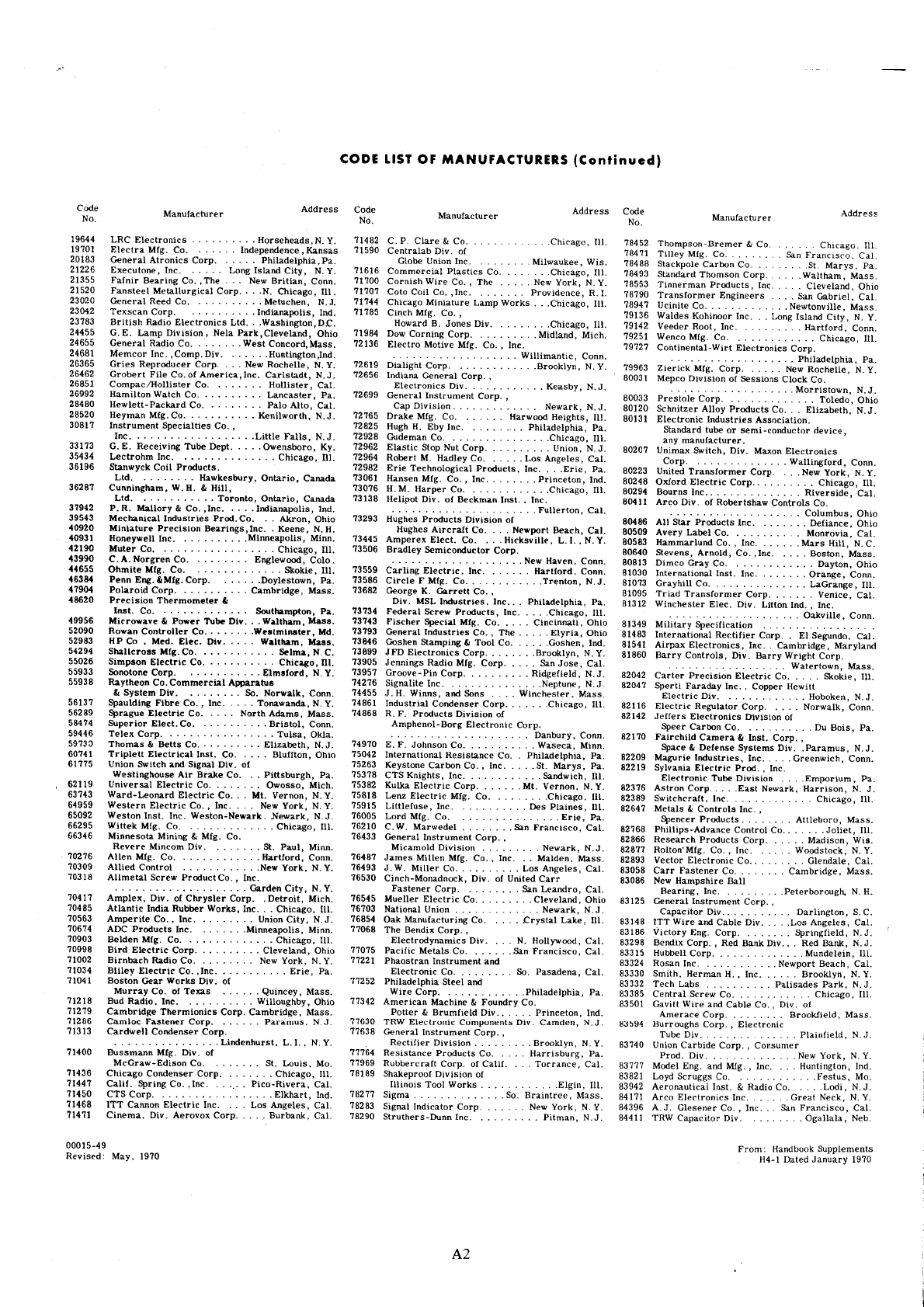
ZY
016I ÄJ"nu"f p"t"c l-'H
sluaqaldd\g looqpu"H : uorJ
qaN r"I"lle3o ^rq Jotrr"d"J /rlUJ IIt'g
'lrJ 'ocsrru"Jd urs tul "oJ JauasalS l v 96tt8
'^ N 'IcoN lsaJC cul scluorlJal3 orJV ItIü8
'f N '!po.I ' 'o3 orp"u D lsul l"crlneorav 296f8
'oy{ 'snlsal oC s8;nJJS pfo.l Izggg
'pul 'uot8urlunH tq ' 8IIil pu" 'äug lapoN ,LL[g
'^ N 'lro^ aaN' ^!q pord
JaunsuoJ ' droJ aprqrxc uorun 0'L0g
I'N 'plarJürEld
'f N'u"u}d '' ruluunc-sJeqluls
'Ä N 'IJoÄ aaN 'dJoJ JolEcrpul lwl(S
'ssEll'aaJlulEJg os " " " 'Eulrs
'lU 'u!SIS " slJoAl looJ srourlll
JO
uOrsr^ro rooldo{Eqs
'lEJ 'a)u"rJoJ JlleJ Jo dloc uelJraqqnu
'"d 'SJnqsrJJ"H ' oJ slJnpold aJuslsrsau
'Ä N 'u^fl@Jg 'uolsr^ro JarJrlJau
0628t
t8z8I
LLZSL
68I8I,
69611
,9LLL
' dJoJ luaunJlsul l"JauaC gtgrl
'f N 'uapu?J ^rq sluauoduoJ cruoJlcalg ,t\UJ 0t9lL
'pul 'uolaculrd .'^!c p'louunJg ,t Jallod
'oJ,{JpunoJ D ourqJ?hl uEJrJauv z}ell
'"d '?lqdtap€lrqd " 'droJ arr^\
pu€ loals "lqdtapElilqd ZiZLL
'I"J 'ruapBs"d oS " " " 'oC cruorlJalg
püE luaunrlsul u"Jlso"qd Izzll
'l"c 'ocslcu"u uals" " " oJ slqaw rrJrrsd gloll
'luJ rp@a,{lloH'N "'^!O'sJlu"u/tpoJlJalg
droJ xrpuag aql g90lL
'III 'ate.I Fls^rJ ' ' 'oJ turrnlc"jnu"I{ IEO }SggL
'f N '{J"6aN ' uorull l"uo!l?N C0l9L
orqo 'puBla^alJ 03 rlJlralg rallanw s'ggl
'I"3 'oJpuEa.l u"S " " ' dJoJ Jauals"J
JJ"C palrun Io ^!o 'Icoup"uoül-qru!3 ocggr.
'l"C 'sala8uv so.l " " oJ ralllw A|f e6t9L
'ss"l{ üaptEl{ ' ' Jul ' oJ 8JW uallur{ sauEf L8}91
'f N rrlJsaaN uorsr^lo plou"Jllil
''dJoJ luaunrlsüI I"JauaC egtgl
'leJ'ocsrJuerJ ues ' ' IapaaJ?lAI Al.J 0IZ9t
'Bd 'arJg oJ '8JII pJo.I 90091,
'lU 'saultld saq " " " 'cul 'asn1e11gr1 91691
'lll 'oBEJntJ' 'oJ äJril clJlralg zua.l glggl
'Ä N 'uoura^ tt4l ' dJoC crllJalg D{InX Zgegl
'lll 'qrrapu"S 'cul ,slqSruXSIJ gltgl
'"d 's,(r?II lS' ' ' ' cul ' oJ uoqr"J auols^al 09zgl
'ed '"rqdlapElrqd oJ aruqslsau lruortaJalul Ztogl
'uurr{ 'Eros?ll 'oJ uosuqof .J.S 0L6tl
'uuoC'ÄJnqu"O
.dJoC JrualJatg SJog-louaqduV
Jo uolsr^rq slrnpoJd .J.u 898ü1,
'lll 'oSErrqJ 'dJoO rasuapuoC l"rJlsnpul lggtl
'ssBI{ 'ralsaqcu!/yt " suos puE'suurlt\ 'H f Sgt}L
'f N 'auqdaN' cul allt"u5ls gl?tl
'f N 'plalJaSpr8 ' ' 'droJ urd-o^@Jo tg6CL
'l"J 'asofurs ' ' ' 'dJof, irt{ orp"U s5uruuaf 906gl
'tr N 'uÄUoorg " " ' droJ sJluoJlJalg (IJf 66ggL
'pul 'uaqsoC ' oJ IooI t turdu"ls uaqsoC g'gel
orqo 'ErJr{II aql ,'oJ sorrtsnput l"rauaC g6lel
oIqO 'rt@urJulC ' ' ' 'o3 8Jn llrcads JaqrsrJ gllgü
'IlI 'o8"rrqJ ' ' Jul 'stJnpord aoJJS I"JapaJ tcLgl
'Ed '?rqdlapqrqd ' "JuI 'sarJtsnput 1St{ .^!O
,'oJ llorr"g .y a3roa5 3996tr
'f N 'uoluaJ,f, ' 'oJ .JJn J alcrrJ 9g9gl
'uuoJ 'pJoIrtH ' Jul 'JrrlJalg äurIrBJ 6ggel
'uuoJ 'uJ^!H aoN 'dJoC rotrnFuoJruas ^alpErg 909g1
'Ä N' I'.I 'alI!^sIJrH. . 'oC .lralg xaraduy gpggl
'lEJ 'qcEa€ UodaaN ' ' oJ UErtrrV saqänH
,o uotsr^rq slcnpold saqSnH 06zgl
016I
'Äry{
rpasr^aU
6t-s I000
'IrJ '{ueqrng ' ' 'dJoJ xo^oJov ^rO '?uourJ ll}Il,
-lrC 'salaäuv so.I 'aut olrlcalg uoweC JII ggtll
'put 'lJetptlg ' ' 'droC SJ.J Og]u,
'l"J 'rra^ru-oJrd cul''oC türJds JIIEC LV|IL
'III 'oSEctqJ 'droJ rasuapuoJ oäaJrqJ gtttf
'ow 's!no1 ls ' ' ' oc uostpg-a?rcJt4l
Jo ^!q trH u@ussng ootlt
'Ä N "l 'I 'lslnquapurl'
'droJ rosuapuoC
llaapJpC elttL
'f N 'snu"J"d " " " 'dJoC
lauals?J coluu3 9gZIl,
'ssElrtl 'a'plJqurJ dJoJ saluolwJaql arptJquEc 6LZIL
otqo 'Iqqänotlrl\ ' ' 'cut 'olpEu png glzlL
'ss"y{ 'daculnb ' ssal Jo oJ Ärrrnlt
,o '^ro $lJom Jrac uolsog ltolt
'Bd 'alrg 'rul"oc JrrlJatg ^alrlg t80tt
'Ä'N 'IroÄ aaN ' oJ o!p"u qcrqurrg z00lt
orqo 'puqa^alc ' droc JrrlJolg prrg 8660t
'ilt 'o8Ec!qJ " .' ' 'oJ 'lgry uapleg CO60l
'uu!W 'srlodEauultt 'rul slcnpord CCV tl90,l,
'f'N '^r!O uoluo " " " . 'rul , oJ allJaduv CgSOL
'ilI 'oä"crqC ' ' cul '$llo^t räqqnU "!pul rlu"llv q8tot
'qrrlil 'lrorlaq' 'dJoJ Jalsr(JqC
Jo '^rC 'xalduv lllol
'Ä'N',tl!Juöpr"C '
'aul ' oC lcnpord 6aJcS lqaullv
'.[, N ':tJoÄ ÄaN' ' ' lorluoJ parllv
'uuoJ 'pJoJUq{' . ' . 'oC SJliI ualtv
'uurlt 'ln"d '1S " " " ^rO uocur!^[ aJa^au
'oJ ''Jyl ? Su,rurlI stosauurl^I
'ltl 'o8"crqJ " " 03 äIn lanf^\
'f N ')tJEAaN :lrEÄaN-uolsa^l cul 'lsul uolsal\
'Ä'N ')tJo.tr
aaN ' Jut ''oJ crJlcalg uralsa^\
'Ä N 'uouJai 'lrrl ' 'oC Jlrlcalg pJwoarl-pJ"fi\
'qJln 'ossoao oJ clrtcalg lEsra^lufl
'€d 'q8rnqsDrd ' oJ a't?Jg JIV asnoq8urlsa/b
Io '^lO IwälS puE qJl!^\S uo(un
orqo 'uolJJnlg ' ' ' ' 'oJ 'lsul lEclrlcalg llatdrrJ,
'f N 'qlaq?zllg . oJ sllag l' sEuoqJ
'"PlO 'esln,L . . 'dJoJ xalatr
'uüoJ 'IolsrJg. . . 'oJ'lJaIg JorJadns
'ssEW 'sw"pv qlJoN . . . . 'oJ Julcalg ant"Jds
'l N'"puBADuoI ' ' cul ' oC arqlJ tulplnuds
'uuoJ 'IlüÄJoN 'oS .' . . . '^tq walsÄS D
f,ruoJtcal3 , droJ sqSnoJJng t6gtg
'ss"f{ rplalplooJg dJoC aazreuv
Jo ^rC ' oO alq"J pu" arrtf DI^BC logfg
'IIl 'oB"rrqJ ' oJ aaJ)S l?rlual gg0tg
'f N 'Ired sap"sll"d ' sqe.I qJaJ Z0Cgg
'Ä N 'u^Dloorg 'cul "H u?uJaH 'qllus 00teg
'IeC 'qrEag lrodaaN Jul uesou 'Zt[8
'IU 'u!alapun!{ " ' 'dJoJ llaqqnH 9lCC8
'f N 'Iueg pau "ÄIO lu"g pau ' dro3 xrpuag 96259
'f N 'pIalJäuIJdS dJoJ 5u! fuo1crr1 ggygg
'I?J 'salaäuv so1 '^rO alq?J pua aJlAi IIt gIICB
'JS'üol8urlJ"q''"arqrolrcedr3
' droJ luaunJlsul l"JauaC
'H N !änoJoqJolad" " " cq'ButJ"ag
Il"g aJrqsdw"H aaN
'sseI{ 'aäplJqu"J 'oC Jauo}sEJ JJ"J
'IrC 'alEpualg 'oJ Jruollralg JolJo^
'Ä N 'Icolspoo^\ 'cul ' oJ 8Jl{.uolloU
'aI^\ 'uosrp"I^l droo slJnpord qcJ"asau
'lll 'tallof ' "oC loJluo3 aru"^pv-sdrllrqd
'ssEll 'oroqalllv slJnpord JaJuadS
' cul sloJluoc t sl"la!{
'III 'oBEclr{C Jul .lJElJqcllas
f N 'uosrJJEH "lr"aaN ls"g dJoJ uorlsv
"d 'unrrodug uotsr^rc aqntr JruorlJalg
'cul "poJd rrrlral3 Erua^lÄS 6lZZg
'uuo3 'qJ-rauoaJ3 ' Jul 'sarJlsnFl alJnSEl{ 60ZAg
'f N 'snuEJ"d lrq sualsÄS asuarac D aJ"dS
' droJ 'lsul D trau?J pllqrJ!?J 0LIU8
'"d 'srog no ' ' oJ uoqJEJ Jaaqs
Jo uo!s!^!q sJtuoJtralg sraJJaf ztlzg
'uuoo 'Il"aJoN ' .' dloJ:o1e1n3ag rrrlcalg 9IIZB
'f N 'ualoqoH ' ^rO JrJlralg
llraoH JaddoJ . .rul r{?pw"J !1JadS l}0Zg
'ItI 'a!)lols ' 'oC crJlJalg uorsrcard JaIJEJ Ato?g
'sszl{ 'ußolJal?^\
'droJ lq8rJ/t\,{JJeg ^rO'sloJluoJ,(JJ"€i 09gIg
puel^J"I/tl' aBprrqu"C .cul,saruoJlcalg x"drM'9lg
'lBJ 'opunSas Ig dJoJ larJqcou l?uoilwJalul egilg
... uorltcrJlrads,{rqIUW 6}tI8
'uuof,'allr^{EO
'JuI ' pul uoll!.I ^r(I 'calg rotsar{rur^\ ZIeIg
'I"J 'acrua^ " " dJoC rawJoJsu?rtr prlJl g6OIg
'III 'agu"JC".l .oJ IIrq^"JC 8l0lg
'uuoC 'aAu"JO .cul .lsul Fuorl"uralul Ocolg
olqo 'uot,(€q .oC ^"rC ocuro ilBoB
'ss"r{ 'uolsog cul,.oJ ,plourv ,sua^als Ot90g
'J N 'IIIH sJ"ll cul "oJ punlJ"uurH eg90g
'l"J'er^oJuoll . , ,oJlal".I Ä:any 6gggg
orqo 'acu"lJaq 'ruJ slcnpord rsls ltv 99'08
orqo 'snqunloJ
'oc slorluoJ aeqstraqou Jo .^ro orJv II'09
'l"C 'aprsra^ru .cul suJnog '620g
'III roS"arqC dJoJ crJloatg prolxo I'Z0B
'^ N 'lJoÄ aoN' droC JauJoJsu"JJ pallun gAZOg
'uuoC'pJoJ8urn"lt . .... .dJoC
scruo4calg uoel{ '^rq 'qcllÄS rurun L0ZOS
'raJnlJ?InuBu fuE
'aJr^ap Jolcnpuor-tuas Jo aqnl pJEpu"lS
'uo-rlErcossv saIJlsnpq JruoJlJalg
't N 'qlaqEzrlg . .oJ qJnpord IoIIV razlruqcs
olqo 'opaloJ ' dJoJ alolsard
'f'N'umolsrJJoW
'oC If,oIC suorssas Jo uolsr^re oJdaIAl
'Ä N 'allaqJou aaN .droJ .tJ!^I lcrrarz
'"d'Erqdlaprlrqd
'dJoC saruoJlf,
aIA lJrA\- IEluaurluoC
'lll 'o8"rrqC . . .oJ 3y4 ocue,11
'üuoC ,proJurH . . .cq ,loou Japaa^
'I N '^llJ pu"lsl äuo.I .cul Joourqol sapl"l\
'ss"W'anr^üolaaN . .....oJalruran
I"J 'la!Jq"9 uES " slaaurSua JauJoJsu?Jl
olqo 'pu"la^alC Jul ,slrnpoJd u?uJauull
' ' '^ro aqnJ,
.dro3 uosuoql prepuzlg
' -oC uqU"J ayod)l.eß
IEJ oJsrJurrJ u€S .... .oJ .BJII,(ollrJ
IIl oS"JlqJ oJ T JauoJü-uosduoqJ
l"J 'uouallnJ
'Jul "lsul uüulJag Jo .^rO lodrlaH gtlel
'IlI 'oS"cnlJ oJ radrBH .I,t.H 9l,0gl
'pul 'uolaJulJd" '' JuI ,.oJ .SJH
uasu"I{ 19001
'"d 'arrg cul 'slanpoJd l?c€olouqJal aug Zg6Zl,
'1"3 'sata.äuv so.l' ' ' ' ' o3,(a1pz11 'rI trrlou t96?1,
'f N 'uorun ' dro3 1ntr1
dols rlls"lg ?9621,
'tU 'oS"cIqC oJ uBuapnC gZ6?,
'"d '"!qdtap"trr{d cul Iqg .H qtnH gz8?t
'IlI rslqSlaH pooar"H " " oJ SIW al"JO ggl,Zl,
'fN'IJ"6aN "" uorsrnrgde3
' dro3 luaunrlsul ItJauaC 669zl
'f'N '.{qsea)l " ^!O scluoJlcalg
, .dro3 lErauaC w"fpul 99gzt
'Ä N 'uÄlloorg' ' . .droC lr{8IIelO 6I9ZL
'uuoC '
rrluEurllrlt\
cqlJEddv IElJJaquoJ'oJ üoaqlIsu 8069S
'l N 'pJor8utg droJ auolouos gt6g9
'lU'ottJtrlJ . . . oJ JrrlJatg uoedqrs 9?OSS
'CN'rul€ .." oJ'tr}ts8orrIEls 16?19
'ssq{ 'uul{ta . . '^tc 'rat3 .pe!{ . oJ dH e8629
'pl{'ralautulr.Ä oJ JallorluoC uraou 060ZS
'88"t{ 'qülltt/h' ' '^to 4nJ Jarcd t a^?aoJJrt{ gs66}
'Ed'uoduu|lrps'..... 03.lsul
t JalewouJaql uo!s!f,ard
'ss"W'a8plJqutC ...'dJoCproJqod
'"d 'uaolsalIoc " ' , "dJoJ'tr!{t'ftrg uuad
'III 'aüo:ls 'oC '8In alruqo
' oIoC '
p@aoläug 'oJ ualäroN 'V 'J
'IU'o5"c!qJ ....oJlatnlt
'uury{ 'sllod€euull{ ' 'cul llaa{auoH
'H'N' auaa){
.'cul' s5ulJuag uolsrJald aJnlElult
{
orqo 'uoJIV ' 'oJ'pojd salJlsnpul IEJ!uq{ca!{
'pul'srlodEü"r[ut. '?uI' oC ry^JoIIEl{ .lf'd
"pw"C'olJquo'oluoJol . ... .pl.I
'll!t{ t H'in'q"qäuluuno
"paBC'orJsluo',(JnqsalöEl{ .' "' " "pl.I
'slanpoJd lroC {cÄ6usts
'IU 'o8?t!qC 'JuJ uqoJlca.I
'I:{ 'oJoqsuaao . . . . 'fdac aqnJ, tu!^lacau .g .g
'f'N'sllsJalll!.I'..'... ...'cul
''oC salllqaads luaunJlsul
'f N'qtroalluax ...'oc'8tytu"uIaH
gzI
t8
98008
8S0C8
06828
LL8Z8
99828
89128
LV9Z8
6S828
91028
SITOL
6000a
9LZOL
9'C99
s6299
260s9
6S619
e
}l.e9
6ItA9
9l,t t9
Iil.09
cet69
9''69
trü89
68299
Ltl99
0?98'
t06rt
t809'
999''
0668'
06I?'
Ie60t
0260'
et96e
zt6Lt.
18e98
96I98
t8t9e
8rr8[
ri80e
02982
08t8?
26692
IS89Z
?9t92
99892
r89te
s99rz
99bbz
08 1,0
?
zwtz
oz0tz
oz9rz
s9tI
a
9ZZl7,
e8I0z
IOL6I
w96r
Iet08
02I08
t8008
rt008
e966r,
LZL6L
l9z6L
z9t6L
9TI6L
Lt68t
06r8r
8S98r.
86t8t
88t8r.
ILWL
z9?81
I"C 'ollv olEd . .
"d 'JalsEcu".l
IsO'ralsllloH ''
'''' ocprblc€d-llalaoH
'''' ocr{cl€/t\uollruBH
" ' oJ JalsllloH/reduoC
'ss"w ruEqll"^\
'"d 's.{J"}t lS
'cul ''oJ 8JI,{
a^rlonl oJlJalg
'qilIl 'pu"Iplll 'dJoJ SururoJ aoq
'III io8EcrqC '^!q saüof .g pJ?aoH
'oc SJII qrur3
'IlI 'o8"clqC ' slJo^l du""I arnl"rurl,I o€eJrqC
'l U 'aJuapr^oJd .cul.'oC IloC oloJ
'Ä N 'IJoÄ aaN ' aq,L ,'oJ aJr^l tlsruJoJ
'IU'o8"JrqC" oJsf,llsqdl",rcJ"uuoJ
'sl/t\ 'aaln"alrt^I cul uorun aqol'
Jo .^rc q"ltlluaJ
'lll'o3"rrql ....oJDaJ"IC d.J
'l N 'lpslslJrS 'cul'"ctJauvJo oJ aM lJaqolc
'Ä N 'allaq@U ÄaN ' ' dJoJ JaJnpoJdau sarl3
'pufuolSultunH' . .. .'^lq duoJ' cul Jocua!^l
'ssElil'pJoauoJlsal\. . . . ..'oJo!p?u lrJauac
orqo 'puBla^alC'\Jed slaN .uorsr^ro du"'I .g.o
'Jq'uo1türqs"Al . pl.I scluorlJalg orpru qsrtrJg
'pul 'sllodEu"rput. . 'dto3 urcsxaa
'f N 'uaqcqat{ . . 'oO paau l"JauaC
'IU roSBclqC N. . . 'droC l"crSrnllslal{ laalsu"J
'uuoJ 'u"rl(Jg aaN . . . aqJ''oC SurJ"ag JruJ?J
'Ä N 'ÄllC puqsl äüo.l . 'rul 'auolncaxg
'rd'Elqdlapvllqd .....'dJoJsJluortvl"rauaC
s"sust'aJüopuadapul . ....'gC äJI,{eJlJalg
'Ä 'N 'sp"aqasJoH
ssaJppv
98I
Zt
t86IL
90r,lr.
VVLIL
l0LIt
00Lrl
9I9I I,
O6qI,L
z89tL
'oN
apoJ
'oN
apoJ
" sc!üorlral3 Ju'I
JaJnla?Jnu"I l
ssaJppv JaJq?"Jnuq^I
ssaJppY raJrgc"Jnutl^l
(p.nultuot)
surunrrvlnNvw
lo lstr too)
'oN
apo J
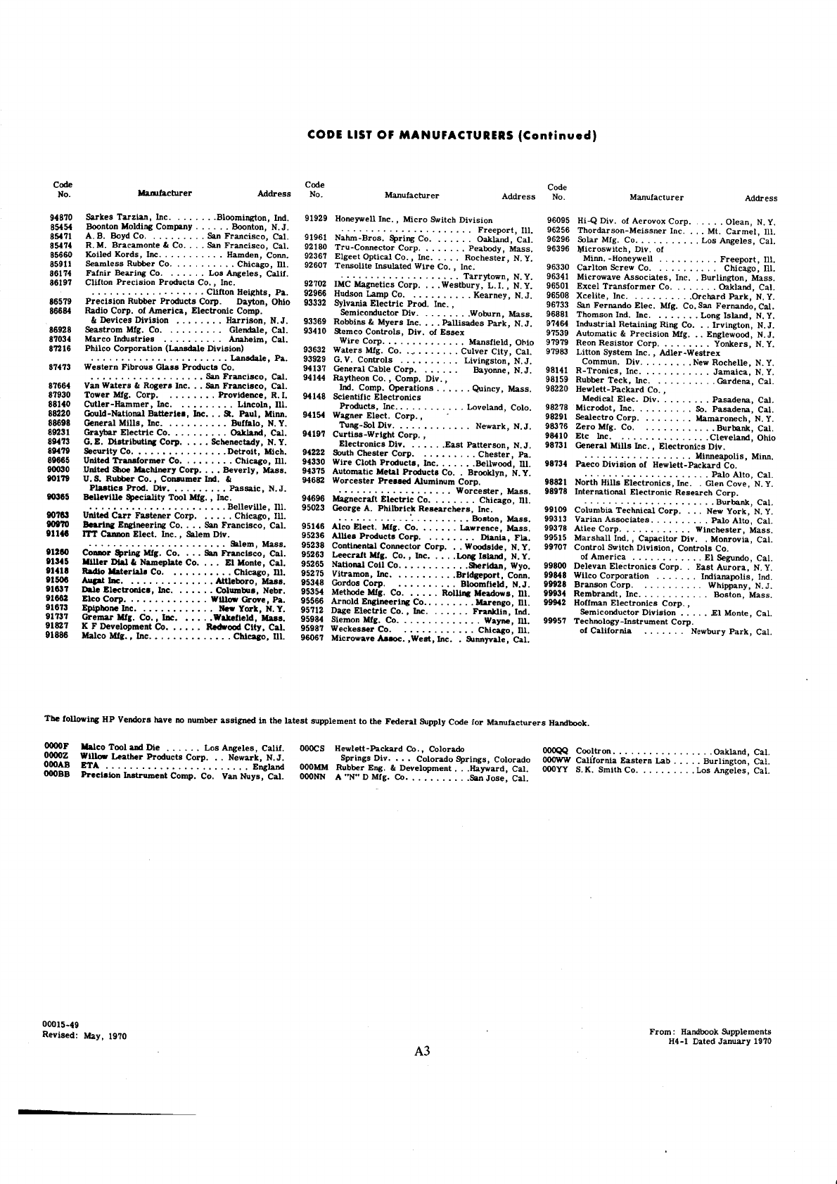
€V
ot6l fEnu"t palec l-tlt
sluauetddqs looqpuEH :uoJJ
'IEC'{Jed,{JnqaaN . ... EwroJll"c ro
'r"r.sara'uvsor.
........ocqrrus.x-s
Är(x' :[3:;::#ä..:;,";il";"f"'?#r",$AJ,ff333
'ItC 'uoliurlJng ' ' ' 'qrl urata"g "IurorlIEC A/6000 op"roloJ ,säulrqg
opzroloC .;.-,nfgJaufiäJ ---'--
'I€c'pu"plBo ''uorrioc b!00o opBroloc ..oc prylcud-palaag 93666
016l .,tq{ :paslreu
6D-9r000
ss0oo
FYOOO
20000
J0000
'dro3 quaunrlsul-r$olouqcel 196,66
'1"3'aluo!{ Ig'''' . uolal^tq
rolcntrtorluas
''d!oC sJluoJlaalg ü"uuoll 21666
'ssr!{ 'uolsog . . . .cul ,lprErqqau t0666
'f 'N 'i(utdd!q^\ .droJ uoffirg 02666
'pul 'sllodwlpq uollrrodroJ oclti\ Sm6a
'Ä N 'EJo$V ls"A 'droC scruorlcalg u"^alaq 00g66
'l"C 'opuntas IS " " . BclJauV Jo
'oc alo4uoc .uo!s!^!q qrlras lo4uoc ,,01,66
'I"C 'r!^oruo!{ '^!C rollcrdEC ,.pul 11eqs:ep g1q66
'ssE!{'Jalsaqcull\ ....,dJoJaallv 01966
'I"C'olIVol"d''' '.' .' aal4cossvu"!rE^ eI866
'l'N.'{roÄ aaN ' ' . 'droJ IEIuqcaI "lqunloC 60166
'IBC'Iu"qrng'
'droC qJeesaU cluorlcalg IEoIlBJaluI g16g6
'l'N.'a^oJ ualg . .JuI
.scruoJlralg sIM qfJoN lzgg6
'I"C'ol[vol"d....
'oJ prBIcEd-llaIAaH Jo
uo!E!^!q oaa"d tgl86
'wlr{ 'sllod"awlw
.^lq saluoJlcalg , .crq sttlt{ IlJilaC lglg6
olqo'FrRIaEIc' .JuI rla oltg6
'I"J '{urqrng' 'op .l1n ora2 91gg5
'I'N 'qcaor€uq{ .dro3 orlcaFag 16ag6
'1tO rwapwed 'oS '' . . . .cul .roporofn gj3g6
'ItJ 'wap"s"d ' .^!C .tatg IBJrpoW
.'oJ pJolc"d-$alÄeH 0ZZg6
'I?C 'aapr"C . . .cq .IraJ raqqnu 69196
'Ä N '?cl"u"f "' 'cul .scluoJJ-u ltlg6
'Ä'N 'auaqcou aaN' ' . . . . . . .^!(I 'unuuoJ
xaJFalt-ralpv .'rul ualsÄS uolt!.I 086t6
'Ä'N '6ra{uoÄ ' 'dJoC
rolslsau uoau 6r,616
'f 'N 'pooaalSug ' ' 'tI!|l uolsloord t crlilolnv 6e916
'f N 'uol5ul^rl ' ' 'oC 8u!U SuruElau lElrlsnpul t9tl6
'Ä'N'püBIsItuo.I " "... .cq .puluoswoqJ 18896
'IEC 'opurureJ wS 'oC 'tI! I 'ralg opuaJal ES ggf
96
'Ä N 'Ir"d pratrJo' " 'aul ,olrlarx 90996
'l"C 'puq{"O 'oC rauroJsurJl laf,xg 10996
'ss"l{ 'uolSullJng 'rul .sals3ssv a^"aorJI!^I Ite96
'III 'o3"c!rtJ ' ' ' 'o3 aarcs uolleJ 0Ce96
'III 'lJodaarJ " Ilaa,(auoH-.uu!!^I
Jo .^rg .qclrAsorcln 96996
'IEJ'solatuvso.I
" " .' "'..oJ .tJ!^Irslos
96296
'lII 'lauJ"J 'l!|I ' . . .cul rausslal^I-uosJEpJor{J 99296
'Ä'N'u"ato' " " .droCxo^oravJo'^!Cb-IIt 96096
lcltrruH srarnp"Jnu"I{ roJ apoC ÄIddns t"rapal aql ol luaualdds l€elq aql uI pil3les" raqEnu ou a^üt alopua^ dH tulmno, eql
'tU 'o'ürWC " " " 'cq .'tt{ orl"t{ 90g16
'1rC 'InC Forpqf " " .'oC paudolaraq g y t2gl6
'sf,tt 'pl.trs|lÄ' ' ' . . .ilf . .oC 'ttf ro.rC fell6
'I'N 'lel r.!t " ' " 'tr4 ilqffg efgt6
'rd'.mrCmm,/n" ....'droCoqa ?90t6
'JqaN'inqmtoJ'.....'cul.trts|l€te.({ r.ggl0
'scq{-rorqlrmv .ilf türy gogfC
'IU 'otalq3 . . . 'oC aFIr.lrt( otDcg fiiti
'1zC 'a$oti tg ' ' ' 'oC.lqdaurN !, ttKt r.1ti gl3fa
'I"C 'o'3tcn{tr rrl8 ' . . 'oC 'ttt{ tutr€ r6uoC OeZfC
'8s"!{'uelE '^I(I uatüS .'aq .tcalg u{urC &LI 9ttl0
'I"C 'ocslcErg uts ' ' ' 'oC tufrailFug tuFr.g 0[A06
'nI 'o8"r!qC ' ' ' ' ' .&oC rauatsg rnC prtFn 89f00
'III 'eInraIIaS'
'cul ''t t{ tol ,$tplce6 aflt^on.g 99C06
'f 'N ']!Es€d ' ' '^KI 'poJd 3.n3rlat
0 'p[I reEmoC ' 'oC req{nu 'S'n dffo6
'esq{ '.{IreÄag' ' ' 'dJoC IrilNat!|f s€ prllull 0An6
'm 'otlclrlC .oC rilJor3ürrJ pqpjl 99909
'qcm 'ltorleq' 'oC /qtnras 6rt68
'tr'N 'Äpalceuetcs ' ' ' ' 'droC tunnqfrFKl .g.C gr.t6g
'I"C 'Fn{ltor ' ' 'oC ctrpalg rrq^"rC IOZ6S
'Ä'N'olllrng "''cul'sn!!tll?raueC 96909
'utr 'lnrd 'G ' ' 'nt 'retrr||"g lworFN-plnoc oz?ß8
'lu 'uIoJUfl '' 'cul 'rauuEH-ranq) 0'188
'I'U 'anapl^ord 'droC 'tI{ raöo& 0g6lg
'IrC 'oJrlJutrJ urs' ' .cul sratoU { sralrÄ nA t99lg
'I!J 'oJgtrwJd uls " "
'oc slcnpoJd 88qc snoJqld uJelsal\
'"d'el"pcuq
(uo!st^!O efrpsur.I) uoll"rodroC oJltqd
'l"C'ulaqwv'.. salrlsnputocrsl{
'l€C 'aFpualC ' ' 'oC 't n EoJle"aS
'f'N 'uo8!rr4l uo!8!^!o 6oc!^t t
'duoJ rluoqr.Ig ,"rlrauv ro .dro3 olpzg
oHO 'uoü"q 'dJoO sFnpoJd rrFlnu uorstceJd
'"d 'slqtlaH uolrlC ' '
'cq "oc qrnpoJd uolslcard uoltllc 16198
'JIIEC 'salatuv so.I " " " 'oJ tulaag rlur"J '1198
'Itr 'ot"c!q3 ' ' 'oC ragqn8 esatu"as 116S0
'woJ 'uap@g ' . . 'aq ,spro)t palloy (D998
'I"3 'ocslcwJJ u?s . . . .oc t aluo@ilrg .I{.u tLwS
'FI"C
'ocalJwJd u"S
.' " .' " 'oJ pIoS 'S V ILISS
'f'N'uoluoog''' . .,(urdqo3*rlplottuoluoog'9'98
'pq 'uo€ulu@Ig .3uI ,q"!znJ salrrs Ofgt6
ssarppv JaJqr"Jn@I I
EL'L8
9tar8
'tor.8
92698
18998
61998
'oN
apoJ
'oN ssarpw
apoc Jaftlrlrml{ 'oN
apoJ
ssaJppv JaJnlJEJnEn
(p.nultuot)
sutrnrrvtnNvu,
Jo rstr
toot
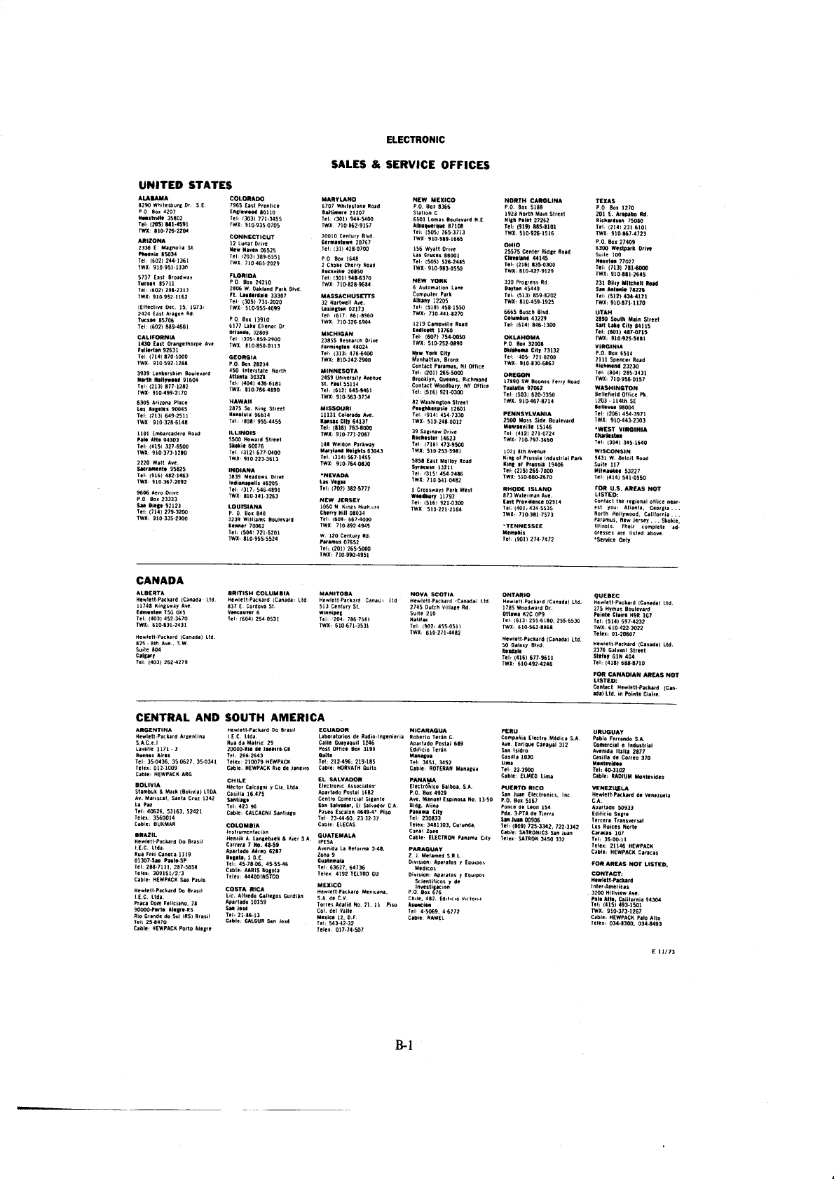
I{
EIIII
Z
t6h.t[0 00t|.fr0 irl.l
onv
opd
xtvdtt| :.tq.l
tlztat€.oI6:tru
r6Le6t (9Ir) :r.l
Fet6 lirrolnrS
,aw !ßJ
'.^v
f.r^ilrN
002€
s.lD.ulJ.t!l
Prqardllal4afl
:lJYlxot
'otlstl lot sEüY lOJ
t!r./rc r3vdttl :.tq!]
rSvdrlff 9tllz:ntrr
rr{0.9€:t.t
lot rarxl
.uot r.lnu rol
Fsr.^3!ajl tr:rral
./r.s o!rupl
et6G oprwd!
.f_1
rt.nrüa^.p ptqrdltati.N
n:haxr^
o.rr^.luotr totovt :.tqtl
z0tt'0:1.1
.a][lrafr
ote o.roc .P rilr.!?
t!32 rxrt !p!r.^v
t.!l$9ut 0 tltrlauo3
'v.s oPrr.J otq.d
lvoonun
zgt 09re
tolts.rrt.l
u.nr !.s sIxoütn :.le.l
zt[t zat a[t.sz/ (60t) ,t.t
s600 ut ws
.r.rl .p v1d.t ..Pa
tst !o.t ep eruo?
a9r5
ros 0 d
'r!t 51ro4r.r1 u?n( u4
oJtt olr:na
?url olwrl:.lqrl
6C.ZZ:t.l
du
0€0t r[rir]
. orprrt !.s
zlc Fn.ral .nluul ..Y
t s $irn o4r.B .rltduoc
nI3d
lrtrYa:.lq.l
ata9t 69ar r.l
[raial
hrot!l or)'trp1
.,tt af{l
!o,;afiF:;ui -
.9 r rorllrar4
ro6'.oi I tottr.dv :uori^{
ro1p.l
\odrnbl
I 3olrr.dv :uor.r^ro
't'as p.ü?ra{ r'l
^Yn9VCVd
{,1 .o.u.d Noullttl ,.tqr!
auoz
t.u.!
'?e.rn3 mll8re:r.t.t
[[totz:t.r
Al! udaa
.utv .tplg
os.tl 0Nrrourd3 trnurt a^v
6Z6t ros o d
't s 'rqtq 01!.94ratl
YiYIYd
16 tl.{to :r.t.l .rf.rf otrod r!!dn!N :.tq!?
,i3'il,t::';i"i ilq us lnem,irq$ ,o," ,,r, ^ ooot* '"
.il?^ t.p to3 ;; I. s!..tqt .!od.@6
oid l|rz 0N plqJ-'_.ll9l ssror 6crj:-oi s. ouerlr.r uoo rr.rd
lt,rrn9 3ot.ilt9 opattv r,l tpll C I r
totnn r4nlxi@ nrr üsoo ils'/s { pr?tredll'lr'ff
n!
ornrr z6rr
'r.r:r -o.c^t!!r99tLi ::.1:l *" "?.Iiifi::i ::T?
eerre r.e.e r.r .,.:lä",j.i:::."''li:1 ssse..ez
Irz.8ez r.r
.,,-,",.,.i'.'B',i!.ri';*it!':.xü'i";'r::r'r'ü':ll
,,,,,iii'J ', ,* 'frii;:lij;]'lili rrus
oo
rq;ir'r'id'*
s!3rtt ,.rq?l Ylgioloc ü!trxns ::tq.a
rt zt tz 09.tr'€a t.t - tt0099€ r:r:t
osld
rr.5t9t uol€Jsl
o.r?d orrrluls l|9lllvf, .r+J tztag tgtcs 9z9ot
:t.l
! l roF^t.S r! !.ta^t6 !q 96 €Zt l.I [d !l
.lurt'! r.'rrruol orl!.t rralcas atCI rnrS
atuls r!)i'/tn .^V
a89t t?Fod
o9.tr.dv gat
9I .lr$sl voll {!r^Io0r
r,rn t tnqo.ts
rällrloisv r'uonr.rl .rll lr! r rut?rl.J rolrak vt^tlol
t@V tVS f! lllHt
!.ttultr XYtllOt 'etq.l oln! HtVllOX :.tq.t o,'3o.{ a! oU tCVdAlff 'ätq.3
zgtc lgt[ :t:l 9tl.6le :g5t.zlz :l.t t]vdtlff 6!mlz .ieral
tatuf, qF! et92.99,:t.l
!t/.1 olrrl9t 66t[ ro8 .:rr0 lsod 89..I.r.r 4 .!t.0000a
619 l?lsod o9.prdv gtel lnüttfig .il.3 6a tlt.tr .p lnu
'9 utr.l olrqo! rL.ru.lut.orplu ap rorolaroqlt ?pn 3 l l
YnoYlYllN u6vnc3 trs.r8 00 pJrt)rdll.ra.H
llv llvdt:N :.lq.a
600t.210:rrt.t
rre0.9c'/e$.gc 9ar0-90,r.r
tar[ r.o.ia
a
' Illt .|.^.1
t.-cYs
?urt!.trV piqr!d1latr.t
vNltN39lY
vcluSl
rv HJ.nos
oNv lvulNlc
'.4ell .utq ur .plt (.p!
-u.1, PrqraJllatra| trqsol
:ollsrl
IOf, SEüY f,VIOYf,€ gOI
0r18-889 {trt) :l.l
tgt xt9 talals
1..4s r!!^tP! 9t[z
'Bt (!Eülc) prttr.dal.tes{
10902{0:r.t.l
aaoe-azt.ol9:tar
aear'/69 {ttt) ,l.r
agl 16fl D!.€ .rut
,r?^.tnog rn0^H 9/z
'plt (.p.o.tt p,.tr.dlt.tarH
J3t30ö
grzt z6t-0l9 ,xrl
lls_llg (9lt):l'1
q.n.l
-p^t8 rr!t!5 09
'pll (!p.u.3J 9r!trld1t.ta.ft
s96i'299.019,rMl
0c99
laa 0tt9 gqz
'tl9) r.1
6d0 3zr ..!tro
',0 pr?ftooa lral
',u (rP.!!' 9)ctr.dll.ta.H
otüYlto
a8tt.Ita 0t9 IAt
ri90.g9r.a06J t.t
ENFI
0tz.l!ns
'pu
3r.lr'^ !rln0 qttz
plt t€Frr?, prltrrJJlsta.H
vrtocs Y^ox
Itse.u9'0t9:tal
rt!1 901 tozr :r.l
t.!!c!!r
1S
Ijnlu.l etE
pI r
r?u?3 0/er)ra
n.ta.H
YAOlrNtn
6(Zt Z9Z 1e0t)
:r.l
l*tt a
t08 elt.s
'a s .^v ql8 - sa0
'pl] (.ps!.c, prctr?dtl.r|.N
tatz.Iet.0I9:rru
Iego.t9z {m9) .r.t 0t9t-z9t ([0t) 't.t
9 rsn.*l sxo 9sl üu.utt
15 ?^opjo3.t
tf0 .^v a.aitury Stttr
tll r.0ru.t, pr.tt?d11.t,.fl pI .plultl pirtrldllatr.t
Yrtfnlof xsrlta vltlglt
vovNvc
IluO.1ürS.
'.^0q. p.lsrt are 5:l3rrp
.p. .tetdu0r ,ra!l sroürilt
-.rtols &!r.r ,at .snurrld
- !ruroltr?t
'poorllroH
quoN
'' '!rtro.9 '.tu.[V :nol rs.
rEo .rut0 t!uort.,
eql
lr?tuoc
:otlstl
loN sEtv 's'n üol
09S0 1'9 {tlr) :t.l
lzaeg
üntrt!{
aIl.Iis
t.oü
l'0ta8
t l[06
ttsNofstI
0t9t-9rt
(roc)
:t.r
rqrwqt
YtNtst^ lstt.
tmzttr.ol6:tar
lt6a.t9r {902)
,t.l
ro085
nr{tr!
!s qlilr'tQzt
'& .rllo pt.u.tag
xot!f,tHSYA
asr0 996.0L
:tel
Ittt-982
(m8) ,trt
o€zez
Fd{1t
prot
r.rr.ds ilra
il19 ro8
.0.a
vtNt9ütA
t895.926.0t6:tAl
9llo-ttt (rü) 1.1
5Itt8 rtlt at.t lttl
t.r4s llrtr {lnos 06aa
HVln
0t[.Iat.o16
ital
Iatt-trt {aI9)
:t.t
gzztl qrtrY f,s
Fq n.{nti rrtg l0z
sr9e.rr
0t6
:IAt
ffina (fI/) :t.t
laoal illr..l
wl rlrns
{!0 tr.qs.fl 6€9
50ttz
14-0'd
tao-ts 0l6
,rar
I0I9 ICZ
(ilZl :t.l
q$l ffitf,{3!ü
.!t oq6.ry .l te
0(zr
ro8
0a
svttt
zttarla lto6l
't t
3!t.ual
f3ss3ttr!r^
€tst tae.ol/
'ttl
S€S!.rCrrt0r):l.l
tl6a0
,t{.!!.04 l..l
'a^v
urui.ltr t(l
oNvrsr looBü
0t9z-099.0r9:xrl
000(.s94
(gtz)
:r.t
$t6I qrrnrd ta lült
lr?d t.rFnpur
.!3sird
ro
turt
..o.^v ql8
lz0l
0s9[.t61.0t(;rr1
tzto.rtz |.rr) t l
9tl9l ,nlrri$f,
prtr.rnog
.Pts srof,
@st
Yrw^t^strxtd
ttts-tgr.oI6,xüt
6€[{29 (t09) :r.r
2926 rtrtFl
ploü
lr.l rauoo8
Ms 068{r
f,@tro
29t9.0e8.0I6:Itr
00z0 lzt ,90t :rrt
zclaa
rtli dsts
8ma€
roa 0
d
vnoHnto
@[1.9t8
(tI9)
it.l
6ZZIt
.rWnp]
'p^t8
qrsng
s999
sz6l.09r-0rE:Iml
Z0z8 65l
{tl9)
'l.l
6119,
!.ttao
'pü
ica/to!
oaa
6Zt5 tat.olt
:ttl
00r0{tt (9rz}
:t.l
qtlr tcataraß
prou
.lpr{ r.tu.C
gasez
otHo
9t5I
9Z6-0IS
ixffl
rolS.sm
(616)
1.1
z9zta
lut.a
{r!H
l..ils
u,rt q!0[ ra6l
t8t9
ro8 0
/
YNtlovt XIüON
99IZ lZ,0tS .x{l
@c0.la6
!9ll):!al
{5{r I lqir
tsaa trld t{.rlsorl I
ztro tt!.0!t tal
9lrz tlt 19lt) trt
Itztl .tnats
prot rolotr tltt g8s
1865 tCa 0l! :IMl
w6.[{t l9lt, t.t
tzgtI rnr{..|
a^rr0
rt!'l!S 6t
ar00 8ta-0G ,xMr
0€ft.tsr Itl6, ,t.l
l09al.!.d.qttn.d
t..rts uolr!rqrtM z8
m€0-Iz6
(9lE):t.t
.)uro r{ IrnqPoon lr?luoc
PUouqr'u sü..n0 .!Itroor€
@6_99 (l0Z) :r'r
.rtrc tx lno.rtd l.?luoJ
ruorS ul4u€w
Iu3 ryor r.il{
o600.zta 0r9 :rat
olm-tsr {{09) :r.l
091€l prtrrt
paou
a[r^durt Stzl
0{?lrrt.oll:tru
69I-89t (819) .trl
90,2t rulq[
tt?d j.tndoo3
.ur1 uorl!{0t.v 9
ttol ütN
09s0-4860t6'rüt
SltZ_949 (909) 'l'I
tmSE r.rntt ri
a^ro nrlt 9st
t99r-6t6.0t6 xMr
tl(['s9a (909):t.1
rcl/8 rtr$lnllt
t'N 9r.i.tnot r.mt I099
I uorFls
99tt ro8 0 d
o3txiil nll
ls6r'66.0l:nr
0@9.t92 {l0Z) :t.r
299{0 rrurnJ
'9t rrnlu.! 0zl ff
56t.Z6t'0tt:IAl
d0t.t99,6091,t.t
't010 nlx r4{l
ir:{trft srury { 090I
r?sütr fllx
t(ts-zgt tzot) 12t
ntal nl
wv tf,.
oeN.tgt.0t6:tM1
99t!r$ {rlar :r.1
$otl .ltt!{ ,r.tlrl
r!r!Jra uopt.a 8tl
aloz Ilt 016 rat
m8.E9l {910 1.1
tglt9 q€ rrf,t
'.^v qtrotot t€llI
tünossti
rt/t.e99.0l6,tfl
l9[.9!9 iZr9)
,r.t
iltgs tn.d ls
.n!r^V ttr!r..'!n 65tZ
YlosSxxri
006z.zrz.0l8:rrl
mt9.9tt lttf) :l.t
tz09t ratl!!0rrj
.^rr0 qrr.c.t 998[z
f,YgtHttn
1069-9Zt.0lr:t4l
0968
191
rll9) :lal
tdz0 rurrr.l
'.^v il.r!.F zt
sEsnHcvssvn
tt96.rzt-0L xar
0l€9.tr6 [0t) :t.l
0s302 .l!!ror
0.0u
^rr$ .toqt a
8r9r rq od
00l0.tat {tf) r.l
(9(02 !r.u0r.!
'p^t8
^r.l!.1 0t@z
19t6.298 0u x[r
00t9tt5 (ls):l.l
{0ala.r.slFg
9?oü:oot3.N[ t0(9
of,nltYi
ta99-996.0t8:XAl
l0?9
IZ' it09) 't'l
zsot ia[.t
pr.^.tnog surilr[ 6gt[
0r8 ro8 0 d
vNvtgnol
t9zt tre 0n Iflr
t63r.9r9
itle) i,.r
9A9r rF0!!!Il
l^Do rrop..t 6gta
Yivtoxl
rr9c.tza.0t6,tür
o0t0-lt9 (alt, trl
9Im9 allals
l..rts prlrofl 0s5
stoxrfll
l9tt_9t6 trc8r :lal
,1t96 ntnpuax
le.4s tu'r'oS qarz
nvttH
68r.99{ 0r :x[1
rtl9-9er {mr):trl
gtot .unt
qrot.trlrr.lot 0st
tfzSz rE o d
Ytso30
4il0.09a 0t8 tflr
0052.691
r90ti t.l
6082a .r[t{
10 iou.Il.trt {at9
0t6at
r0g 0d
660r.s96.019,tn
0t0' I€( (90t) 'r:1
loe$ lqr.tiq tt
,^r8 t/.d 9!?q!o fl $ta
0lzrz r€ .0d
YOttdJ
6402.59r'0t(
ttl
1s99.63[
rCOZ,
]t.r
9Z9S QIX rat
.^r0 rau.t zl
rnf[ffNtoJ
@z-9ea.0t6:tru
az[ 6tz
rrt{)
:r.r
tzrz6.l.!! q
taaaa
roa
0t
z60a.t9t 0t5 ,Ifll
[9tI Zlt I9l6' 'l'l
92196 .lrü.rq
'.^! nr{ ozaz
oazt.ar€-0r6:rnr
0099-(z€ 19tr),t.l
[09!6 axt alla
pto! or.pllr.qul t0tI
ttI9.8Z[-0I6 XAl
llSe'6t9 (tla):lrl
!ru6 tattlll lol
.t.tJ luorov 90€9
04lz.56t 0t5 ,ttl
ztzl.ttT lelal :t.t
10916
paaranal {pat
,r.^.tnq @r{raturt 646€
rszl.z5s
0I6 ,ttl
o@l ot8
{tIl' :l'l
l[95 o.rr.ilr,
.^v adroqtalu.ro tral octl
YINÜOJIlY!
I99t 688 (209) :i'r
90(91 s.sl
'p! uolcry
tsst Datz
er6t gr 'r.0 .^Ir.lBl
z9il zs6.0l5,xal
altz t6z (209r
t.t
lltst ucr.nl
r.r9.ort tr!3 /taq
0tat.ß6 015 xal
r9al ttu (209)
,t.l
x6t trq
.ts.rtoü.n I sez
vxozttY
Ea-$r!ti ,ru
90/0.9€6-016
tal 169r{r (g) ,t.1
gsr[.ta(
(toei :trr zo8!t
.[r{3ri
0ll0l toar.tlll toar ro0 0 a
.rtu./dF.lS96t jS )otrnF.lr\A6Zt
6VIO103 YmnY
srlvls otrriln
s3crJjo tct^uts ? st'tvs
3r[ourc313
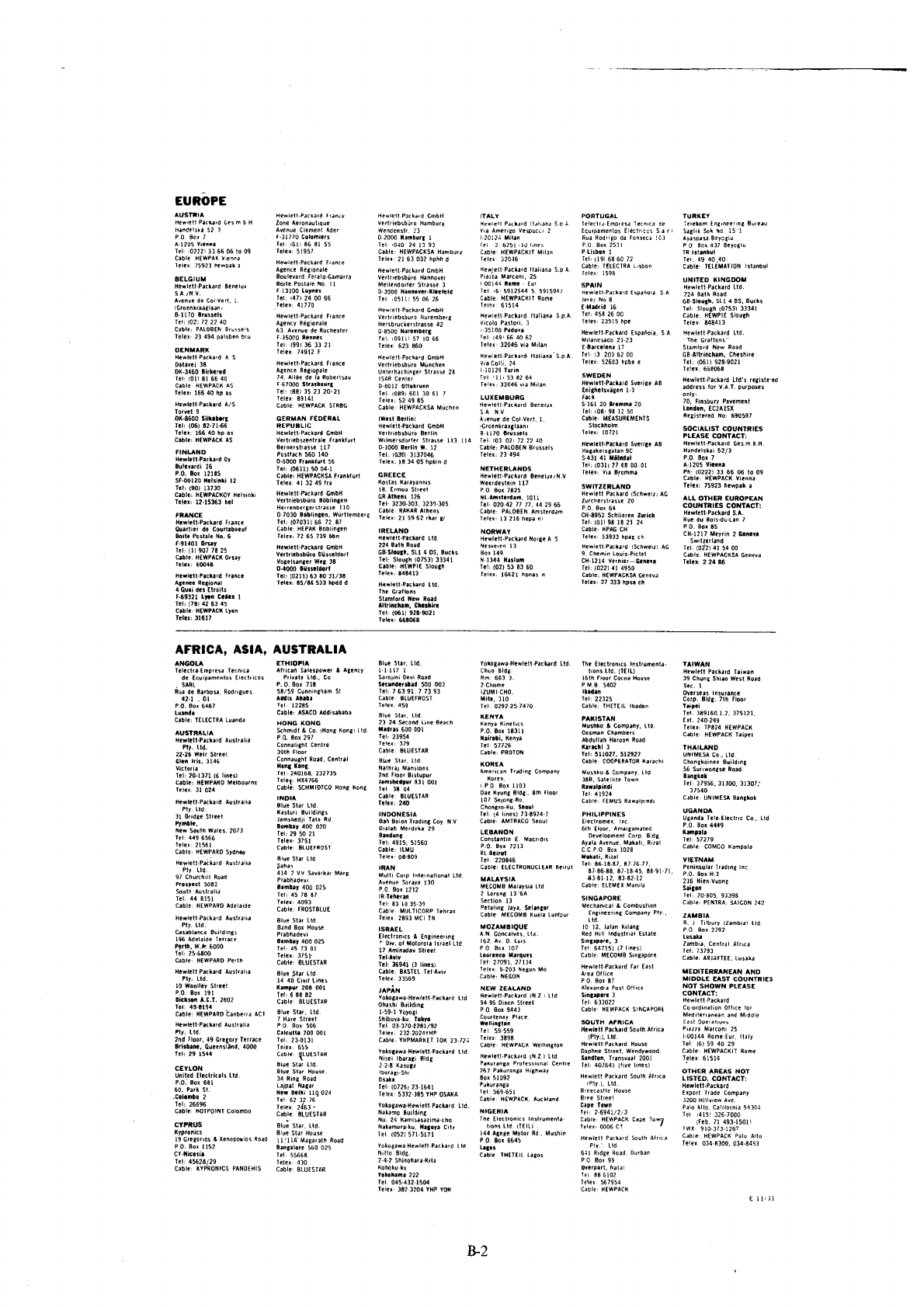
Zfl
tl,ll l
t6t8 t[0 00t9.][0 rälal
o|v DtPd
ytvdillH alq?l
.92l
ate-0t6
xür
rt09i.€6t r{ q3l)
000t.92e
istt rä1
$ev6 Prur0,rtet olt! 0t?d
'a^v
M.r^tlr*
00zf
^u?duol ep€rr
tr0drl
pretr?dlletaat
:tcvlNoc 'otlsrl
loN svtüY usHto
,19t9 ratat
.wo8 ltltvdMlN .tq?l
6Z 0t 65
(9) t.l
ItsI rnt .uoU tttOO.l
gz ruorretr
?rzera
suortsr.d0
lsEl
alpprw
ple r€eueD.lrp.w
ror
.1r0 u0rteurpio 0l
pretrPdtlata0N
:ICYINOJ
lsvfld NAoHs loN
s3rütNnotr tsE 3100tn
oNY NV3trYüülltO!h
?let.l'lllllllv :.tqel
l6t€a:ral
.rrtv le4uot trquPz
ttrrtrl
z6tz ros 0 J
Dlr iErqüP7)
Irnqrrl I I
YIAtrY?
ztz No!lvs vltNtd :arqea
86et6 908 02 'ral
lrl!$
Suon^ !.![ 9IZ
IHrot 0J
)ut rurprrl r.tnru!u3a
nvNtlt^
elecoet 0llol r.tqrl
6tats t.I
at.dut
6t" ro8 0'd
'pI of, 1rtr.ll.al.l epr?tn
voNY0n
tottu.g vslfrttn rtq.a
0tqta
.10€l[ 00il[ 9!5te r.r
lollo'a
peou
.stuoruns 9s
turplrng..urotSuoql
'pll o! vslwrN0
otrntYHt
r.d'.1 ,SVJtlH .tqtl
x?vJülH tzSdr jr.r.l
6tz
0rz lrl
'tat9tE zr09l6te:r.l
!{!1
iooü qtl tpte .dJoa
srutrntut stalra^o
I r.s
prol li.f o.rqs tu.q3 6a
u?N'.1
Dr?lred
n.tf.H
!YtrYl
,f,v3illa atqea
,96a9q ratel
z0l9 88 lal
LPteN
!0rr.^0
66r08 0d
u€qrno
peoS
atprS
l19
pI .
^tJ
urrilv qtnos
p)srrrd llalr.H
, ll 9000 rtlrl
ldor ao.l ylvdfi]H atqel
tla/1n69-z:tal
ürot .dtJ
tsarls rrrS
asnoH
aIt?]ra/8
'plt I
rlnr
e)!tv qtnos pretred
nara.H
(s.url
a^q)
lt9l0r it.l
I00z ls2^su.rl lrlt!rs
'pooa^p!.il 1aä4s .uqdeo
.s.oH pretrPd
natraN
'plr lrru)
€)ulv !tn0s 9r.trcJ n.tr.t
Y'üJV HInOS
t|od!9Nis lavaalH arq?l
zzoet9 tal
a ./odtlots
a)r|0 Fod rrpu?r.lv
a8ros 0d
errlt0 ?rr!
lrrt r.J trPtreJllat4rH
arodelu'S
8Wof,ln ;alqPl
(s.u
I t) Itlt19:rat
C'.rodtto'S
äl?tsl rPr{snput lrN p.8
tü?|y u?tet Zt 0t
'pD
' .ld luedüoa t!raa!r8ul
uo'ls.auoc
t t.riu.qrah
tlodY9Nls
?lruew
Ilnlll rilq?l
zl.zt [8 zr tS ao
'lt l6 88 9t 8I.t8 0r'98.a8
'It 9t t8 't8 8t 98 ir.l
lerrl tr'l'l
SZotros 0d3a
r.?rl rt?tew anua^v.r.rv
tp I drot ruirdot.^ao
p.l?u?treuv ro0tj ql9
rol r.@otrarl
slNtdatltHd
't!Ldr?ael
snnlt :.tq!l
tz6It rrl
!!u!aFr.ü
urol 3tr|.tts s8t
p| ^usduot
I o{qrnl
rqJ?r.x tolvutdool ltqrl
rzSzlt lz0nt:r.r
t t{rrjat
p?od
!00itH q!|npqv
sr.q04l !!ü5o0
'0n lu?duot ! o{snt
rvlsttvd
rotel 11llßl .lqrl
r.&l
9199 ro8 0 d
urqs.w pt rotofr .r.t! til
'(llllr pll suorl
'?tuaü.4sut
s)ru0{r.E .ql
vrct9tx
p!.tirnt rtvJalß.ta?3
t99
69S r.r
"!?hl''J
26019
r08
lerqirH ?tuernt.! t9Z
a{u.c t.!orssrlord
etu.rnted
on (
r tl p,r!r?J lt.t|.H
uott!rilaü yldMtH arqel
€68t raral
699 69 er
u.lluil.t
'.)rrd ^eu.t/n0l
,rt6 !o8 0 a
taa)ts
üoil0
96 t6
plt z N) pr.tr.d uatorß
ONYIY]Z AfN
N09lN i.rqea
0n !ot.N toz 9 r.t.l
ilil4'160/? lel
3.nhr!tr o.u.rn0l
aor ros 0 d
sint 0 ^r zql
'PD s.^Flo09 NV
!oÖranYzotr
,0turt.s .{?t Sul.lrd
et u0rlr.s
v9,tt tuorot z
pll ?ri^.1!tr gn0!1tr
Yts^vlYtr
1.r.3 üvltlnNoülllll :.tq?l
9t80za tal
u/rag tu
ilat ro8 0 !
3rpr..w t utru.FUof,
NONYIIl
Ino.5
0lvülwt.rrq?l
l.tz68.tt (s.!rt r) trl
iro.s.t.ortuoql
'oü
tuor.s r0l
ioot,
qtS tptg tunrt aeo
tortro0 0al
'€.1o,
Iu?d0ot rurpal uerr.u!
Ytt0y
l0l0üJ:alq.l
gLtts.t.\
?Iurr'!q.r!tN
lt[9r ro€ 0a
srr.urt rlu.t
YIN]X
,o^ dffl ,02[ ztt .ret.t
,0sI-ztt.5D0,t.l
zzz rut{0t0r
ßt.nt0q0!
eIt-?rPqoulqs
z.' a
'3P18
ollrN
ptI pr?ir?d
ilata.H
eiletotol
lllg tt9 lzg0) ral
^tr3 .l.trx nt-l)n0.{.N
oqr'?uQ€s€$@!, 'z 0N
tu.9trng 0u€teN
'plt p/ttlrd IrlaaH.Pr?lotoA
vrvso dNl 58f za09 rrtat
rt9l ez
r9zt0).tir
!tti0
rQs.rt.reqt
etns.y g-Z
?
tPrs rtsrrqr r.srN
'pn 9rrtJ?dJlrtaaH €r?loto^
izt ez y0l ltxlvndHl:rrq.l
dllDz0z zIa 'r:la1
a5lr8?a.0rt.t0 tar
olryl 'nt ?tnqr{s
rtolol 1.6!.1
turptrnS rqs?qO
Ptl D/.tr.df l.lr3x,?,rtq0l
NYdYI
69lac:trl.l
^r^v
1.1 lllsv8 :.lq?!
6.o!t c) lt69t 1.1
^t^t1.r
laa{s ^rpculuv A
plt te?rrt
el0r0tow
t0.H0 !
türa.urtuj ? ir,uo{r.tl
llYtsl
Nl nn t68z rrr.l
uer{.1 d!0ltltnn aLqet
6C 9C
0r t8 ;rä1
r?r.q.l-üi
ztzt ros 0 !
0el s^sroS 3n0.^v
9ll lc!oleü,al!r drol rltnW
NVUt
608_80.rrt.l
nnll:.lqel
095I9
j9I6' 't.l
tuntu.S
6Z.t.praw {?t?'0
^ f, ^o9
turte,l uoroS
qeo
vts!NooNl
otz:rrl.l
u!lslnle .rqPl
to 8t t.I
100 l[8 rnat{rs.f
r.d.ts18 roo! plz
suorsuen larqteN
pll rels .qt
tvlstntS .rqel
6lt:r'rar
t56ta ilet
t00 009 rrill|
qre.o aür]
puor.s
tz ta
plt ,.ls 3nt8
69t:fla1
lSoUtnts rtq?l
[6 €t I 16 [9 I :t.l
e00 009 tasr.t$r.s
p?08
r^.0 ruilorEs
ItilIt
'Pn
rqs..r8
tvlstnlS 3lqel
0et:ralal
89959 t.l
EZO 099 .rot!tu4
p?ou ql?rslet !il, il
asnor rrts 3.8
'pn r?ts änt8
uvlslnl9 .rq.l
' egtz ral,r
,9t aa z9 t.L
rz0 0ll !{rrd r.N
rttt{ Itdr€l
p?o! tlru tt
'ilroN rPts.ntE
'pn r?ls .nl€
sltslnü'.rqPa
qq9:rrr'l
ret0.cz:rar
r00 00t !trnlr!
905 r08 0 d
lr.{s.r.B I
pll rcls.nrg
IrISlnls lrqll
zt st 9 iFl
100 aoz ,.tütt
s.u'l lsrl 0t tl
pll r.ts a.t8
r!1slnt8'.rq.3
q9re:tal.1
I0 tt sr,jal
920 00t raQuoe
r^.pPqqera
rsnoH ro8 pue€
plt ,els ..t8
tntsls0ül'.tqel
t60t:rtr'I
t8 8t st:t.t
!20 00ü Ir{0.0
r^apPqq.rd
tr.W rst,P^?S
r^ Z ttt
reqes
pn r.ts.nls
lsoul0l8:.lcel
I9la ir.t.l
1,09 5z:t.l
0?0 mt raqDoa
pu €t01
rlp.qsü?,
sru'ptrn6,rt5!r
pn iets.ntg
Ytoxl
tuox tuoH 0Cl0tnNf,S :.tq?a
99ltIl:r.lar
seazez 89I0tz l.l
lüu t{oa
t.4!.3'Fot lqtneuuol
rooB {t6a
a/lual lqtlleuuol
t6z ros D J
plt rtuoy ruoff, oa
? lDruqrs
9|ox 9Nox
€qrq.srPPv
03!sv :elq.l
58aZI lt1
!t.ll tlDtl
l5 ü?!turu(nl 69/85
8u ror'0 a
o! pll .F^lrd
Iru.l! ?,.rods.rrs utrrrlv
YtdorHtl
vr-lvulsnv
stHt0NvJ sf,tN0udlr,atq.l
6Zl?Z9St f.\
r!r.r!N tc
z9ll ro8 0 d
p?ou
sotedo!rx ? so!01.r9
6l
sruordlt
snüatJ
oquotol
lNt0Jt0H .tqel
s99Z:ter
z o!00t!4.
ls lrsd 09
t89
r4.0 d
'pu qoltr.B pelrun
NOtltS
ttsl 6a ;t:l
000r .plqrruarno .ilrq4t
m?!al lrorarg 6t ,ooB puz
'plt tta
e,t?rtsnv
pr.lr.dlt.rrrH
rlt t'aqu€]. owdtlF i.lq!l
r6la-6t:r.l
z09z ,l.l,l !.3trt!
t6l ro8 0'!
l..rls l.Iooa 0l
'9lt ru
e'te4snv
prPtnJ n.ti3a
ql)ad
0lvdMlH :alqrl
0089 s2 ,t.1
ooog {a siia
anr.l äprPla0v
961
sturprrng
Pr0.tqss.!
'pll ru
erre4rnv
pretrcJll.rN.t
.prelapv
0üvdttN 3tq.J
l9I8
tt'l.l
Prterls.v
qlnos
290! lr.drord
pcot llq)rnqt t6
ptl ^ta
e't.rtsnv
pi?tFd llatd.N
&uP(S
0UVdtlN,alqel
t99tz rat.1
9999
6tt ir.t
etoz satrr qt.os a.N
'nqu&
l..rls.tpu€ Ie
.pn .rld
.rr.4snv preltrdll.tN.N
tzo l€ r.t.I
ruJ.oqta{ 0uvdrlff :{qlJ
{s.!rt 9)
lt[t.02:t.1
rrolt!^
9il[ ltt !.t!
IDtS r!.A ga.ZZ
'9ll ^tJ
ert.{3n! pr!tt?d1latr.ff
YIlYüISOY
epü.nl
v8lclttI:1qe!
Itwnl
ttrg r00 0 d
t0 I-u D
s..t'rpot'.rqr.8 .p ?nü
lUVS
rorr{r.8 rolü.u?drn5l it
firur.I rsrrdut c4r.t.l
Y]@TY
'vtsv'vclulv
u?oaqrtllllHl,arqP3 0rrl9a.a6a0:ta\
9ZtZZ:t.L ott .t!t
u.Dlat 0H3 lwnzl
z0$ ond ä0oqcz
ts.or ?or0l rm{J qtgr '€ a09 ür
(lBtJ pll suo4 tpto onql
.?l!run45utst'!o{raB.qt plt pi.trpJ1t.la.f,.?aeiot0l
9S te z :r.lel
?^aua! vsytlddtH .tq.l
00 tt It {alo)
,ral
9u.lr.rlrrs
tr.!.! a urrl3fl llzl-ff1
qsro8
0d
I u0t.np.sroo.p.nu
't s prrtr?d{rta.H
:lcvtf,ot s3Blf,noc
NvfaoSnt ü!Hro tlY
I llda.q €269! :t.t.1
eu!.r^ lSvdals r.rq.]
60
0l s 99 €e (?zz0)
qd
tuar^ qozl v
I r08 0a
t/?! r?tst.pue{
I q u s.9 pr.lr.J tr.taeg
:l?lrtrof tsvtrld
s]üttrnot lstlvtcos
461069:oN
pai.lslt.u
xslvzSl '!!!uor
luaur^!d tunqrurl 0t
:IIUo
s.rodrnd
tv^ rot ssarPp?
parilsrt.r s,pn prst)sditata.H
890899
r.lat
t206.826 {t90' rtat
arqsa!3 uqrür4tv 89
p.08 rrl trotuels
..s!ouP)9
aql.
'ptr p/etred
I3t{.N
aIt8t8 r.r3l
qlnols lldalH ,.rqel
It€a[ (€9lOr
qtn0lS ]l.l
stln8 isc t lts qtrois 09
pPo! qt?€ rzz
'plt pr.tr.d lltta.r
nootxrx ollin
lnq!.lsl N0lllSllll i.lq.l
'0t_0t 6t r.1
tnqo.t!t ür
ntto^.8 l€r ro8 0 d
nlt0I.8 6.d!eIr
L !I o! t6 lrlt?s
n.r,ng tu i..0't!l do!:t)l
llrunl
q3
esdq
€ae lz :x.l.l
c^4u.9 vslf,vdalH :.lqe!
0t5' It (u20,
tal
rr.rt! rarurrl tIzt Hl
l.l)ra.srn01
0reat 6
9V lr.aq)sJ tr?tr.a trata3H
qr trdq ca6€9 r.t.r
ff? 9VaH
'äl!?l
r, Iz 8l t6 rl0r
,t.I
{.!trt !.i3rq)s z!68-fl!
t9ro8 0d
0?.s5.4!raqrrhu
9V
rr'a{q)s) pr?tt.d n.traH
oNnü!lrrMs
:uuoi8 ?rl iralal
I0 00 89
Ia rlt0) :r1l
rr9rt!ü rr ler-s
c6
u.t.riralPtPa
EV .rD.^S prqrld1r.tr.8
IZa0l:r.l.t
ülo{t)ots
sI{3nr8osvlr'.rqcl
09
zt 86 80) r.r
0z ls[.rt 0z tgl s
l1.J
[-t u.t?^sta{ttu]
8V .tr/.^s pr?tJrdll.tMa8
N3q3AS
. aqdq
e09?9
rtar.l
00 z9 toz er lal
ll to!l.l,l€ l
tz.tz op.sau?rrn
v s Prog€0rl
prelre!ltat{a|
.dq
SIEEZ
irär.1
00
9z 8lt:l.l
9t r!rr?n.l
I oN :araa
NIYdS
86ll iralar
uoqt,l
YBllllll :alqe!
zt 09 89 L6tr
ital
I u.q3rt
a
[92 ro8 0 d
tci err.uol P0 o.rpot ?n8
I
r ?
s s.rLrlrrB totüa0edrntl
a9 s)'u).1 Psa,dut Prträtäl
rY9nltoa
u t.uoq Iz99t :räl.l
09 c8 e9 IZ0)
:l.t
0ntrr| ttet N
6tI ro8
tt u.r.^raN
s v.tr0N pr.tr?!1l:la.H
lYtüoN
u.daq
9lz aI ir.lal
0e!.lsuv tlgolvd :arael
99 6a tn ar LL ar oao 't.!
ll0l rttr.ltut-lN
9a8t loe 0 d
aII !r.lsapr..M
^ N/rnrau.8 0r€lr€dll.rr.H
soNntlBrfN
t6, ez:r:l?1
trassdrg
llgolva r.rqe!
0t zz al tao
t01 tet
ltrirrrt 01il g
ru.?tteejr!30r5/
I lr.^.rot .9 .nuar!
^N VS
InrauaS
prPtr€d
ll.lM.H
9ünan3xn1
u?ttw
?r^
9r0ea iätal
19 z0 tq 
's'n
Nt
c3rNrud il006-06rt0
oüvxgvd
Et
-- JlgTlvlgH
.
;';
!,;
+.-F--.i-=.',..-.-*!l
