Huawei Technologies 201705EM300 eM300-8a User Manual
Huawei Technologies Co.,Ltd eM300-8a
UserManual.wiki
>
Huawei Technologies
>
201705EM300 User Manual
User manual
Navigation menu
Upload a User Manual
Namespaces
Wiki Guide
HTML
PDF
Info
Views
User Manual
Discussion / Help
Navigation
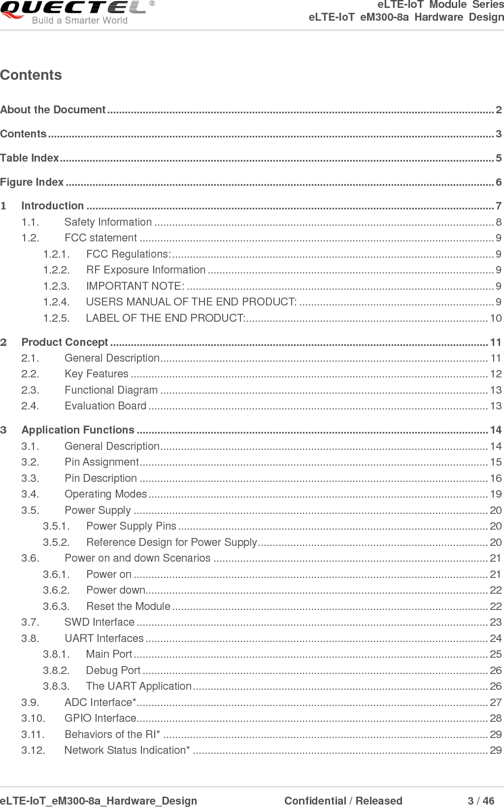
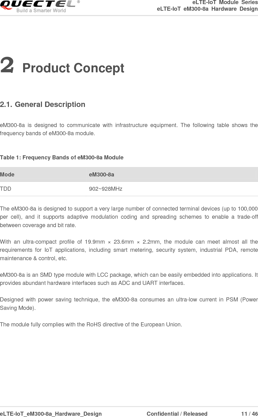
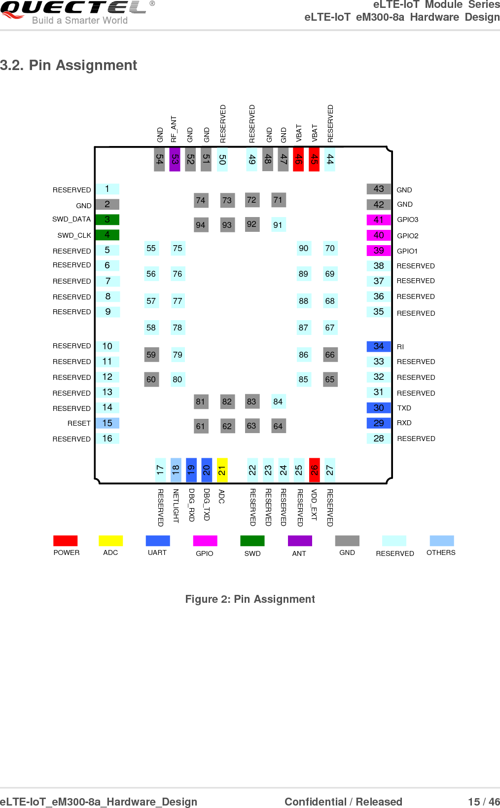
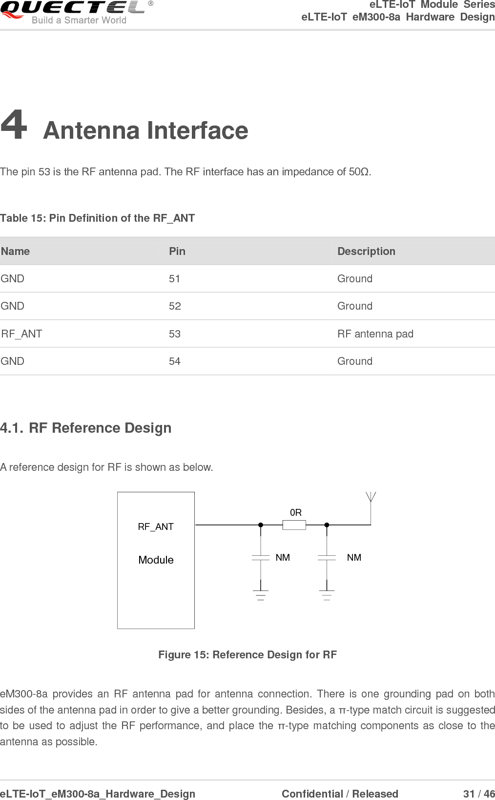
![eLTE-IoT Module Series eLTE-IoT eM300-8a Hardware Design eLTE-IoT_eM300-8a_Hardware_Design Confidential / Released 33 / 46 Figure 18: Coplanar Waveguide Line Design on a 4-layer PCB (Layer 3 as Reference Ground) Figure 19: Coplanar Waveguide Line Design on a 4-layer PCB (Layer 4 as Reference Ground) In order to ensure RF performance and reliability, the following principles should be complied with in RF layout design: Use impedance simulation tool to control the characteristic impedance of RF traces as 50 ohm. The GND pins adjacent to RF pins should not be hot welded, and should be fully connected to ground. The distance between the RF pins and the RF connector should be as short as possible, and all the right angle traces should be changed to curved ones. There should be clearance area under the signal pin of the antenna connector or solder joint. The reference ground of RF traces should be complete. Meanwhile, adding some ground vias around RF traces and the reference ground could help to improve RF performance. The distance between the ground vias and RF traces should be no less than two times the width of RF signal traces (2*W). For more details about RF layout, please refer to document [2].](https://usermanual.wiki/Huawei-Technologies/201705EM300/User-Guide-3387253-Page-34.png)
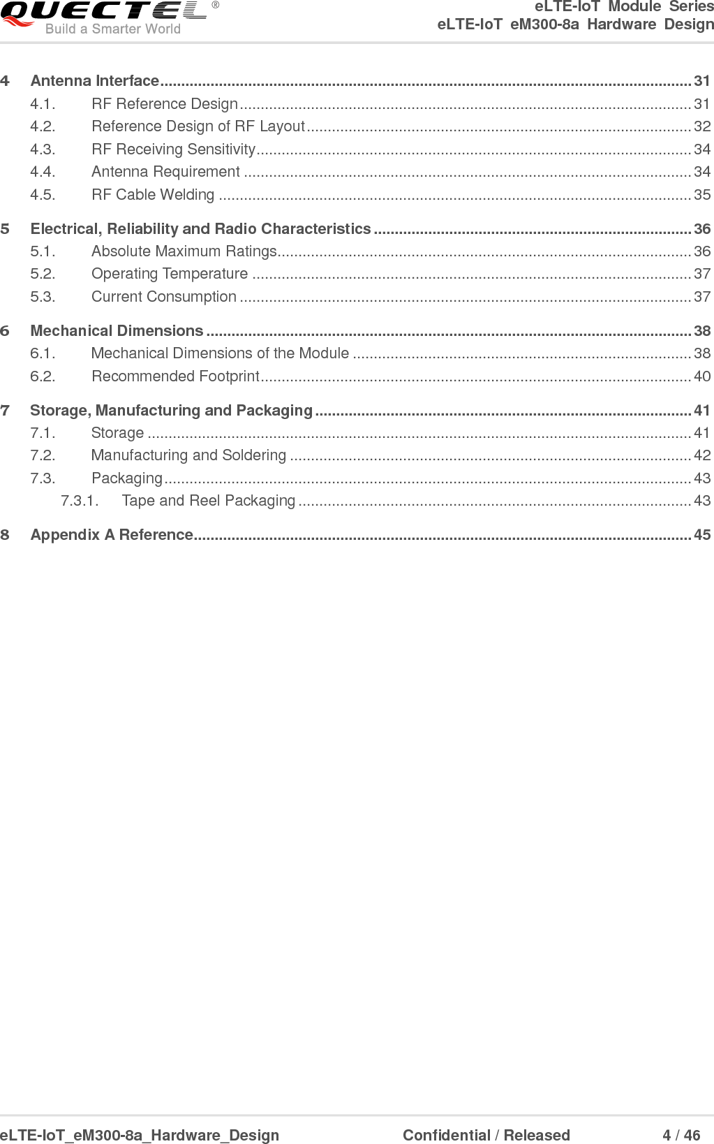
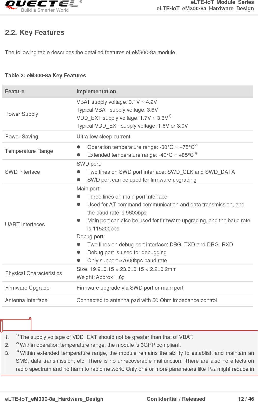
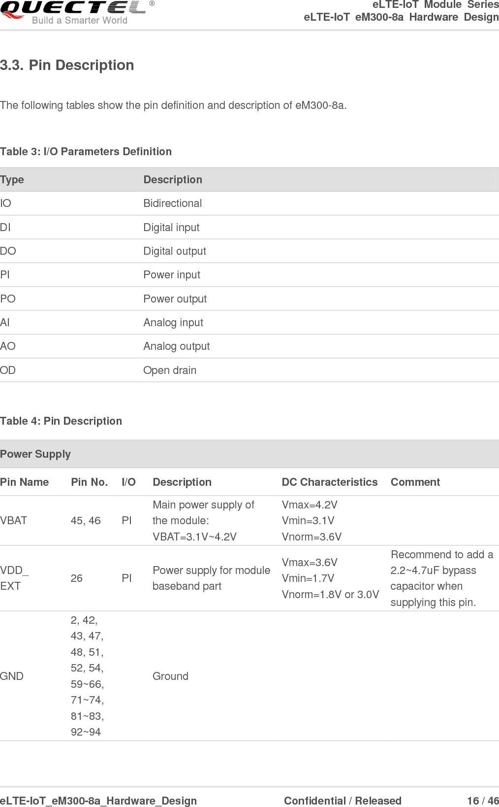
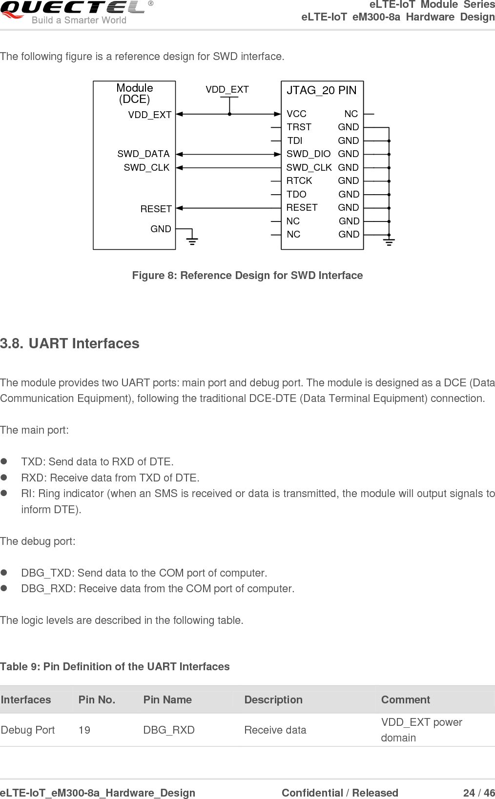
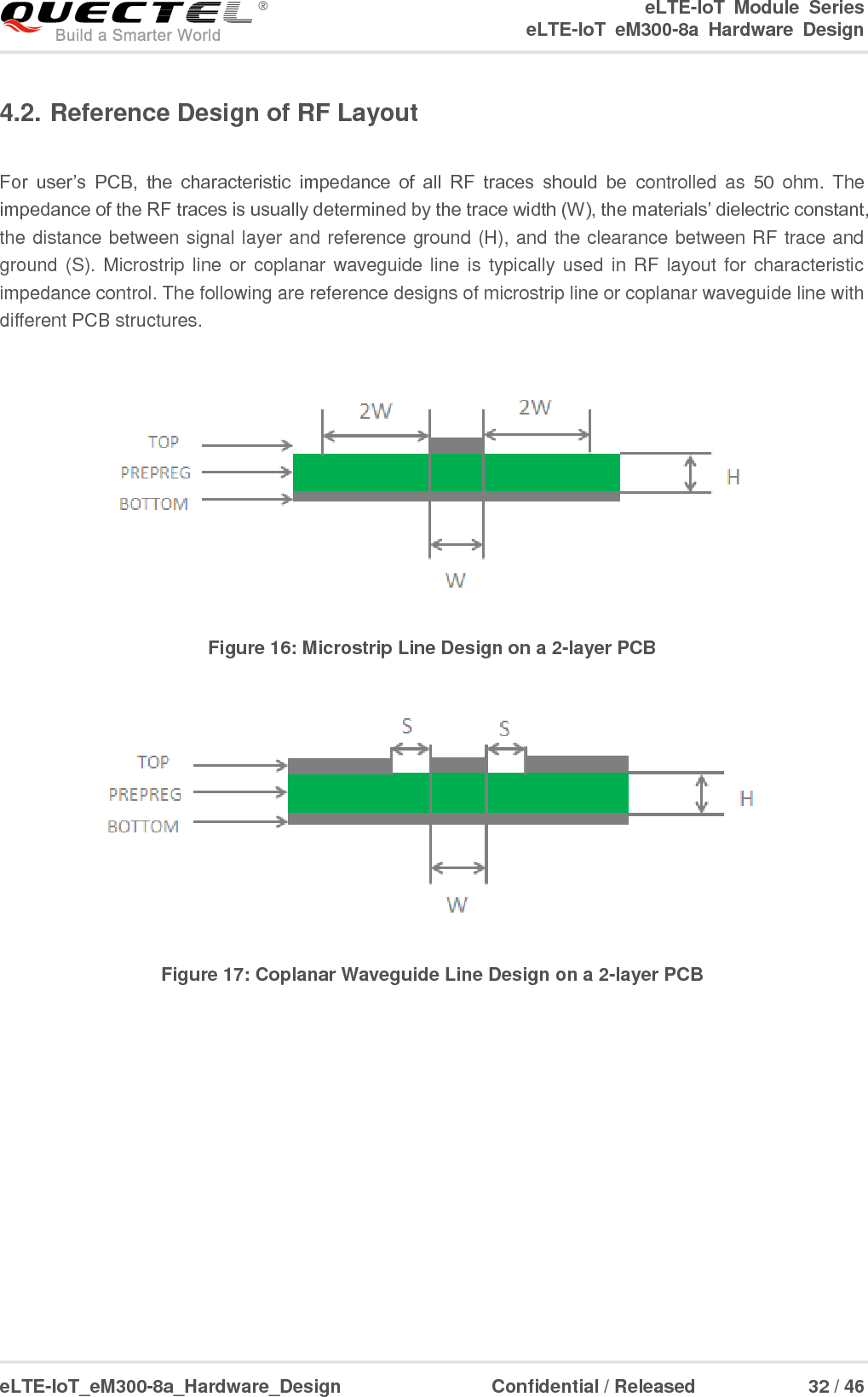
![eLTE-IoT Module Series eLTE-IoT eM300-8a Hardware Design eLTE-IoT_eM300-8a_Hardware_Design Confidential / Released 42 / 46 7.2. Manufacturing and Soldering Push the squeegee to apply the solder paste on the surface of stencil, thus making the paste fill the stencil openings and then penetrate to the PCB. The force on the squeegee should be adjusted properly so as to produce a clean stencil surface on a single pass. To ensure the module soldering quality, the thickness of stencil for the pads at the bottom of the module should be 0.15mm. For more details, please refer to document [1]. It is suggested that the peak reflow temperature is 235 ~ 245ºC (for SnAg3.0Cu0.5 alloy). The absolute max reflow temperature is 260ºC. To avoid damage to the module when it is repeatedly heated, it is suggested that the module should be mounted after reflow soldering for the other side of PCB has been completed. Recommended reflow soldering thermal profile is shown below. Time50 100 150 200 250 30050100150200250 160ºC 200ºC217070s~120s40s~60sBetween 1~3ºC/sPreheat Heating CoolingºCsLiquids Temperature Temperature Figure 24: Reflow Soldering Thermal Profile During manufacturing and soldering, or any other processes that may contact the module directly, NEVER wipe the module label with organic solvents, such as acetone, ethyl alcohol, isopropyl alcohol, trichloroethylene, etc.](https://usermanual.wiki/Huawei-Technologies/201705EM300/User-Guide-3387253-Page-43.png)
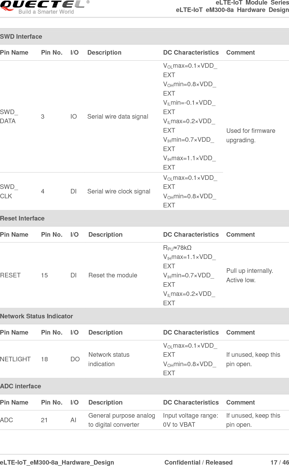
![eLTE-IoT Module Series eLTE-IoT eM300-8a Hardware Design eLTE-IoT_eM300-8a_Hardware_Design Confidential / Released 45 / 46 8 Appendix A Reference Table 22: Related Documents Table 23: Terms and Abbreviations SN Document Name Remark [1] Quectel_Module_Secondary_SMT_User_Guide Module Secondary SMT User Guide [2] Quectel_RF_Layout_Application_Note RF Layout Application Note Abbreviation Description ADC Analog-to-Digital Converter DCE Data Communications Equipment (typically module) DTE Data Terminal Equipment (typically computer, external controller) eLTE-IoT Evolved Long Term Evolution Internet of Things I/O Input/Output IC Integrated Circuit Imax Maximum Load Current Inorm Normal Current kbps Kilo Bits Per Second LED Light Emitting Diode PCB Printed Circuit Board PSM Power Saving Mode RF Radio Frequency](https://usermanual.wiki/Huawei-Technologies/201705EM300/User-Guide-3387253-Page-46.png)