Huawei Technologies 201705EM300 eM300-8a User Manual
Huawei Technologies Co.,Ltd eM300-8a
User manual


eLTE-IoT Module Series
eLTE-IoT eM300-8a Hardware Design
eLTE-IoT_eM300-8a_Hardware_Design Confidential / Released 1 / 46
Our aim is to provide customers with timely and comprehensive service. For any
assistance, please contact our company headquarters:
Quectel Wireless Solutions Co., Ltd.
Office 501, Building 13, No.99, Tianzhou Road, Shanghai, China, 200233
Tel: +86 21 5108 6236
Email: info@quectel.com
Or our local office. For more information, please visit:
http://www.quectel.com/support/salesupport.aspx
For technical support, or to report documentation errors, please visit:
http://www.quectel.com/support/techsupport.aspx
Or email to: Support@quectel.com
GENERAL NOTES
QUECTEL OFFERS THE INFORMATION AS A SERVICE TO ITS CUSTOMERS. THE INFORMATION
PROVIDED IS BASED UPON CUSTOMERS‟ REQUIREMENTS. QUECTEL MAKES EVERY EFFORT
TO ENSURE THE QUALITY OF THE INFORMATION IT MAKES AVAILABLE. QUECTEL DOES NOT
MAKE ANY WARRANTY AS TO THE INFORMATION CONTAINED HEREIN, AND DOES NOT ACCEPT
ANY LIABILITY FOR ANY INJURY, LOSS OR DAMAGE OF ANY KIND INCURRED BY USE OF OR
RELIANCE UPON THE INFORMATION. ALL INFORMATION SUPPLIED HEREIN IS SUBJECT TO
CHANGE WITHOUT PRIOR NOTICE.
COPYRIGHT
THE INFORMATION CONTAINED HERE IS PROPRIETARY TECHNICAL INFORMATION OF QUECTEL
CO., LTD. TRANSMITTING, REPRODUCTION, DISSEMINATION AND EDITING OF THIS DOCUMENT
AS WELL AS UTILIZATION OF THE CONTENT ARE FORBIDDEN WITHOUT PERMISSION.
OFFENDERS WILL BE HELD LIABLE FOR PAYMENT OF DAMAGES. ALL RIGHTS ARE RESERVED
IN THE EVENT OF A PATENT GRANT OR REGISTRATION OF A UTILITY MODEL OR DESIGN.
Copyright © Quectel Wireless Solutions Co., Ltd. 2017. All rights reserved.

eLTE-IoT Module Series
eLTE-IoT eM300-8a Hardware Design
eLTE-IoT_eM300-8a_Hardware_Design Confidential / Released 2 / 46
About the Document
History
Revision
Date
Author
Description
1.0
2017-03-17
Bryant CHEN/
Mark ZHANG
Initial

eLTE-IoT Module Series
eLTE-IoT eM300-8a Hardware Design
eLTE-IoT_eM300-8a_Hardware_Design Confidential / Released 3 / 46
Contents
About the Document ................................................................................................................................... 2
Contents ....................................................................................................................................................... 3
Table Index ................................................................................................................................................... 5
Figure Index ................................................................................................................................................. 6
1 Introduction .......................................................................................................................................... 7
1.1. Safety Information ................................................................................................................... 8
1.2. FCC statement ........................................................................................................................ 9
1.2.1. FCC Regulations: ............................................................................................................. 9
1.2.2. RF Exposure Information ................................................................................................. 9
1.2.3. IMPORTANT NOTE: ........................................................................................................ 9
1.2.4. USERS MANUAL OF THE END PRODUCT: .................................................................. 9
1.2.5. LABEL OF THE END PRODUCT: .................................................................................. 10
2 Product Concept ................................................................................................................................ 11
2.1. General Description ............................................................................................................... 11
2.2. Key Features ......................................................................................................................... 12
2.3. Functional Diagram ............................................................................................................... 13
2.4. Evaluation Board ................................................................................................................... 13
3 Application Functions ....................................................................................................................... 14
3.1. General Description ............................................................................................................... 14
3.2. Pin Assignment ...................................................................................................................... 15
3.3. Pin Description ...................................................................................................................... 16
3.4. Operating Modes ................................................................................................................... 19
3.5. Power Supply ........................................................................................................................ 20
3.5.1. Power Supply Pins ......................................................................................................... 20
3.5.2. Reference Design for Power Supply .............................................................................. 20
3.6. Power on and down Scenarios ............................................................................................. 21
3.6.1. Power on ........................................................................................................................ 21
3.6.2. Power down.................................................................................................................... 22
3.6.3. Reset the Module ........................................................................................................... 22
3.7. SWD Interface ....................................................................................................................... 23
3.8. UART Interfaces .................................................................................................................... 24
3.8.1. Main Port ........................................................................................................................ 25
3.8.2. Debug Port ..................................................................................................................... 26
3.8.3. The UART Application .................................................................................................... 26
3.9. ADC Interface* ....................................................................................................................... 27
3.10. GPIO Interface ....................................................................................................................... 28
3.11. Behaviors of the RI* .............................................................................................................. 29
3.12. Network Status Indication* .................................................................................................... 29

eLTE-IoT Module Series
eLTE-IoT eM300-8a Hardware Design
eLTE-IoT_eM300-8a_Hardware_Design Confidential / Released 4 / 46
4 Antenna Interface ............................................................................................................................... 31
4.1. RF Reference Design ............................................................................................................ 31
4.2. Reference Design of RF Layout ............................................................................................ 32
4.3. RF Receiving Sensitivity ........................................................................................................ 34
4.4. Antenna Requirement ........................................................................................................... 34
4.5. RF Cable Welding ................................................................................................................. 35
5 Electrical, Reliability and Radio Characteristics ............................................................................ 36
5.1. Absolute Maximum Ratings................................................................................................... 36
5.2. Operating Temperature ......................................................................................................... 37
5.3. Current Consumption ............................................................................................................ 37
6 Mechanical Dimensions .................................................................................................................... 38
6.1. Mechanical Dimensions of the Module ................................................................................. 38
6.2. Recommended Footprint ....................................................................................................... 40
7 Storage, Manufacturing and Packaging .......................................................................................... 41
7.1. Storage .................................................................................................................................. 41
7.2. Manufacturing and Soldering ................................................................................................ 42
7.3. Packaging .............................................................................................................................. 43
7.3.1. Tape and Reel Packaging .............................................................................................. 43
8 Appendix A Reference ....................................................................................................................... 45

eLTE-IoT Module Series
eLTE-IoT eM300-8a Hardware Design
eLTE-IoT_eM300-8a_Hardware_Design Confidential / Released 5 / 46
Table Index
TABLE 1: FREQUENCY BANDS OF EM300-8A MODULE ............................................................................... 11
TABLE 2: EM300-8A KEY FEATURES .............................................................................................................. 12
TABLE 3: I/O PARAMETERS DEFINITION ....................................................................................................... 16
TABLE 4: PIN DESCRIPTION ........................................................................................................................... 16
TABLE 5: OVERVIEW OF OPERATING MODES ............................................................................................. 19
TABLE 6: VBAT, VDD_EXT AND GND PINS .................................................................................................... 20
TABLE 7: RESET CHARACTERISTICS ........................................................................................................... 22
TABLE 8: PIN DEFINITION OF SWD INTERFACES ........................................................................................ 23
TABLE 9: PIN DEFINITION OF THE UART INTERFACES .............................................................................. 24
TABLE 10: LOGIC LEVELS OF THE UART INTERFACES .............................................................................. 25
TABLE 11: PIN DEFINITION OF THE ADC ....................................................................................................... 28
TABLE 12: PIN DEFINITION OF THE GPIO INTERFACE ............................................................................... 28
TABLE 13: BEHAVIORS OF THE RI ................................................................................................................. 29
TABLE 14: WORKING STATE OF THE NETLIGHT .......................................................................................... 29
TABLE 15: PIN DEFINITION OF THE RF_ANT ................................................................................................ 31
TABLE 16: RF RECEIVING SENSITIVITY (MCS-1, BLER <10%) ................................................................... 34
TABLE 17: ANTENNA CABLE REQUIREMENT ............................................................................................... 34
TABLE 18: ANTENNA REQUIREMENTS .......................................................................................................... 34
TABLE 19: ABSOLUTE MAXIMUM RATINGS .................................................................................................. 36
TABLE 20: OPERATING TEMPERATURE ........................................................................................................ 37
TABLE 21: CURRENT CONSUMPTION ........................................................................................................... 37
TABLE 22: RELATED DOCUMENTS ................................................................................................................ 45
TABLE 23: TERMS AND ABBREVIATIONS ...................................................................................................... 45

eLTE-IoT Module Series
eLTE-IoT eM300-8a Hardware Design
eLTE-IoT_eM300-8a_Hardware_Design Confidential / Released 6 / 46
Figure Index
FIGURE 1: FUNCTIONAL DIAGRAM ............................................................................................................... 13
FIGURE 2: PIN ASSIGNMENT ......................................................................................................................... 15
FIGURE 3: REFERENCE CIRCUIT FOR THE VBAT AND VDD_EXT INPUT ................................................. 21
FIGURE 4: TURN-ON TIMING .......................................................................................................................... 21
FIGURE 5: TURN-OFF TIMING ........................................................................................................................ 22
FIGURE 6: REFERENCE CIRCUIT OF RESET BY USING DRIVING CIRCUIT ............................................. 23
FIGURE 7: REFERENCE CIRCUIT OF RESET BY USING BUTTON ............................................................. 23
FIGURE 8: REFERENCE DESIGN FOR SWD INTERFACE............................................................................ 24
FIGURE 9: REFERENCE DESIGN FOR MAIN PORT ..................................................................................... 25
FIGURE 10: REFERENCE DESIGN FOR DEBUG PORT ............................................................................... 26
FIGURE 11: LEVEL MATCH DESIGN FOR 3.3V SYSTEM .............................................................................. 26
FIGURE 12: SKETCH MAP FOR RS-232 INTERFACE MATCH ...................................................................... 27
FIGURE 13: BEHAVIORS OF RI WHEN A URC OR SMS IS RECEIVED ....................................................... 29
FIGURE 14: REFERENCE DESIGN FOR NETLIGHT ..................................................................................... 30
FIGURE 15: REFERENCE DESIGN FOR RF .................................................................................................. 31
FIGURE 16: MICROSTRIP LINE DESIGN ON A 2-LAYER PCB ...................................................................... 32
FIGURE 17: COPLANAR WAVEGUIDE LINE DESIGN ON A 2-LAYER PCB .................................................. 32
FIGURE 18: COPLANAR WAVEGUIDE LINE DESIGN ON A 4-LAYER PCB (LAYER 3 AS REFERENCE
GROUND) .................................................................................................................................................. 33
FIGURE 19: COPLANAR WAVEGUIDE LINE DESIGN ON A 4-LAYER PCB (LAYER 4 AS REFERENCE
GROUND) .................................................................................................................................................. 33
FIGURE 20: RECOMMENDED RF CABLE WELDING .................................................................................... 35
FIGURE 21: TOP AND SIDE DIMENSIONS OF EM300-8A MODULE (UNIT: MM) ......................................... 38
FIGURE 22: BOTTOM DIMENSIONS OF EM300-8A MODULE (UNIT: MM) ................................................... 39
FIGURE 23: RECOMMENDED FOOTPRINT (UNIT: MM) ................................................................................ 40
FIGURE 26: REFLOW SOLDERING THERMAL PROFILE .............................................................................. 42
FIGURE 27: TAPE DIMENSIONS ..................................................................................................................... 43
FIGURE 28: REEL DIMENSIONS ..................................................................................................................... 44

eLTE-IoT Module Series
eLTE-IoT eM300-8a Hardware Design
eLTE-IoT_eM300-8a_Hardware_Design Confidential / Released 7 / 46
1 Introduction
This document defines the eM300-8a module and describes its hardware interface which are connected
with your application and the air interface.
This document can help you quickly understand module interface specifications, electrical and
mechanical details. Associated with application note and user guide, you can use eM300-8a module to
design and set up mobile applications easily.

eLTE-IoT Module Series
eLTE-IoT eM300-8a Hardware Design
eLTE-IoT_eM300-8a_Hardware_Design Confidential / Released 8 / 46
1.1. Safety Information
The following safety precautions must be observed during all phases of the operation, such as usage,
service or repair of any cellular terminal or mobile incorporating eM300-8a module. Manufacturers of the
cellular terminal should send the following safety information to users and operating personnel, and
incorporate these guidelines into all manuals supplied with the product. If not so, Quectel assumes no
liability for the customer‟s failure to comply with these precautions.
Full attention must be given to driving at all times in order to reduce the risk of an
accident. Using a mobile while driving (even with a handsfree kit) causes
distraction and can lead to an accident. You must comply with laws and regulations
restricting the use of wireless devices while driving.
Switch off the cellular terminal or mobile before boarding an aircraft. Make sure it is
switched off. The operation of wireless appliances in an aircraft is forbidden, so as
to prevent interference with communication systems. Consult the airline staff about
the use of wireless devices on boarding the aircraft, if your device offers an
Airplane Mode which must be enabled prior to boarding an aircraft.
Switch off your wireless device when in hospitals, clinics or other health care
facilities. These requests are desinged to prevent possible interference with
sensitive medical equipment.
Cellular terminals or mobiles operating over radio frequency signal and cellular
network cannot be guaranteed to connect in all conditions, for example no mobile
fee or with an invalid USIM/SIM card. While you are in this condition and need
emergent help, please remember using emergency call. In order to make or
receive a call, the cellular terminal or mobile must be switched on and in a service
area with adequate cellular signal strength.
Your cellular terminal or mobile contains a transmitter and receiver. When it is ON,
it receives and transmits radio frequency energy. RF interference can occur if it is
used close to TV set, radio, computer or other electric equipment.
In locations with potentially explosive atmospheres, obey all posted signs to turn
off wireless devices such as your phone or other cellular terminals. Areas with
potentially explosive atmospheres include fuelling areas, below decks on boats,
fuel or chemical transfer or storage facilities, areas where the air contains
chemicals or particles such as grain, dust or metal powders, etc.

eLTE-IoT Module Series
eLTE-IoT eM300-8a Hardware Design
eLTE-IoT_eM300-8a_Hardware_Design Confidential / Released 9 / 46
1.2. FCC statement
1.2.1. FCC Regulations:
This device complies with part 15 of the FCC Rules. Operation is subject to the following two conditions: (1) This device
may not cause harmful interference, and (2) This device must accept any interference received, including interference that
may cause undesired operation.
This device has been tested and found to comply with the limits for a Class B digital device, pursuant to Part 15 of the FCC
Rules. These limits are designed to provide reasonable protection against harmful interference in a residential installation.
This equipment generates, uses and can radiated radio frequency energy and, if not installed and used in accordance with
the instructions, may cause harmful interference to radio communications. However, there is no guarantee that interference
will not occur in a particular installation If this equipment does cause harmful interference to radio or television reception,
which can be determined by turning the equipment off and on, the user is encouraged to try to correct the interference by
one or more of the following measures:
-Reorient or relocate the receiving antenna.
-Increase the separation between the equipment and receiver.
-Connect the equipment into an outlet on a circuit different from that to which the receiver is connected.
-Consult the dealer or an experienced radio/TV technician for help.
Caution: Changes or modifications not expressly approved by the party responsible for compliance could void the user„s
authority to operate the equipment.
1.2.2. RF Exposure Information
This device complies with FCC radiation exposure limits set forth for an uncontrolled environment. In order to avoid the
possibility of exceeding the FCC radio frequency exposure limits, human proximity to the antenna shall not be less than
20cm (8 inches) during normal operation.
1.2.3. IMPORTANT NOTE:
This module is intended for OEM integrator. The OEM integrator is still responsible for the FCC compliance requirement of
the end product, which integrates this module. 20cm minimum distance has to be able to be maintained between the
antenna and the users for the host this module is integrated into. Under such configuration, the FCC radiation exposure
limits set forth for an population/uncontrolled environment can be satisfied.
Any changes or modifications not expressly approved by the manufacturer could void the user's authority to operate this
equipment.
1.2.4. USERS MANUAL OF THE END PRODUCT:
In the users manual of the end product, the end user has to be informed to keep at least 20cm separation with the antenna
while this end product is installed and operated. The end user has to be informed that the FCC radio-frequency exposure
guidelines for an uncontrolled environment can be satisfied. The end user has to also be informed that any changes or
modifications not expressly approved by the manufacturer could void the user's authority to operate this equipment. If the

eLTE-IoT Module Series
eLTE-IoT eM300-8a Hardware Design
eLTE-IoT_eM300-8a_Hardware_Design Confidential / Released 10 / 46
size of the end product is smaller than 8x10cm, then additional FCC part 15.19 statement is required to be available in the
users manual: This device complies with Part 15 of FCC rules. Operation is subject to the following two conditions: (1) this
device may not cause harmful interference and (2) this device must accept any interference received, including interference
that may cause undesired operation.
1.2.5. LABEL OF THE END PRODUCT:
The final end product must be labeled in a visible area with the following " Contains TX FCC ID: QIS201705EM300". If the
size of the end product is larger than 8x10cm, then the following FCC part 15.19 statement has to also be
available on the label: This device complies with Part 15 of FCC rules.
Operation is subject to the following two conditions: (1) this device may not cause harmful interference and (2) this device
must accept any interference received, including interference that may cause undesired operation.

eLTE-IoT Module Series
eLTE-IoT eM300-8a Hardware Design
eLTE-IoT_eM300-8a_Hardware_Design Confidential / Released 11 / 46
2 Product Concept
2.1. General Description
eM300-8a is designed to communicate with infrastructure equipment. The following table shows the
frequency bands of eM300-8a module.
Table 1: Frequency Bands of eM300-8a Module
The eM300-8a is designed to support a very large number of connected terminal devices (up to 100,000
per cell), and it supports adaptive modulation coding and spreading schemes to enable a trade-off
between coverage and bit rate.
With an ultra-compact profile of 19.9mm × 23.6mm × 2.2mm, the module can meet almost all the
requirements for IoT applications, including smart metering, security system, industrial PDA, remote
maintenance & control, etc.
eM300-8a is an SMD type module with LCC package, which can be easily embedded into applications. It
provides abundant hardware interfaces such as ADC and UART interfaces.
Designed with power saving technique, the eM300-8a consumes an ultra-low current in PSM (Power
Saving Mode).
The module fully complies with the RoHS directive of the European Union.
Mode
eM300-8a
TDD
902~928MHz
eLTE-IoT Module Series
eLTE-IoT eM300-8a Hardware Design
eLTE-IoT_eM300-8a_Hardware_Design Confidential / Released 12 / 46
2.2. Key Features
The following table describes the detailed features of eM300-8a module.
Table 2: eM300-8a Key Features
1. 1) The supply voltage of VDD_EXT should not be greater than that of VBAT.
2. 2) Within operation temperature range, the module is 3GPP compliant.
3. 3) Within extended temperature range, the module remains the ability to establish and maintain an
SMS, data transmission, etc. There is no unrecoverable malfunction. There are also no effects on
radio spectrum and no harm to radio network. Only one or more parameters like Pout might reduce in
Feature
Implementation
Power Supply
VBAT supply voltage: 3.1V ~ 4.2V
Typical VBAT supply voltage: 3.6V
VDD_EXT supply voltage: 1.7V ~ 3.6V1)
Typical VDD_EXT supply voltage: 1.8V or 3.0V
Power Saving
Ultra-low sleep current
Temperature Range
Operation temperature range: -30°C ~ +75°C 2)
Extended temperature range: -40°C ~ +85°C 3)
SWD Interface
SWD port:
Two lines on SWD port interface: SWD_CLK and SWD_DATA
SWD port can be used for firmware upgrading
UART Interfaces
Main port:
Three lines on main port interface
Used for AT command communication and data transmission, and
the baud rate is 9600bps
Main port can also be used for firmware upgrading, and the baud rate
is 115200bps
Debug port:
Two lines on debug port interface: DBG_TXD and DBG_RXD
Debug port is used for debugging
Only support 57600bps baud rate
Physical Characteristics
Size: 19.9±0.15 × 23.6±0.15 × 2.2±0.2mm
Weight: Approx 1.6g
Firmware Upgrade
Firmware upgrade via SWD port or main port
Antenna Interface
Connected to antenna pad with 50 Ohm impedance control
eLTE-IoT Module Series
eLTE-IoT eM300-8a Hardware Design
eLTE-IoT_eM300-8a_Hardware_Design Confidential / Released 13 / 46
their value and exceed the specified tolerances. When the temperature returns to the normal
operating temperature levels, the module will meet 3GPP specifications again.
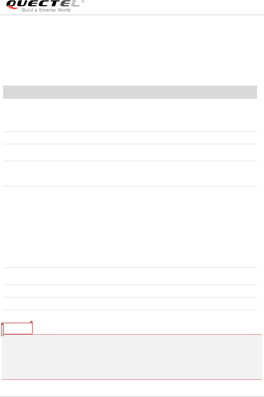
2.3. Functional Diagram
The following figure shows a block diagram of eM300-8a and illustrates the major functional parts.
Radio frequency
Power management
Peripheral interface
RF_ANT
Switch
RX_SAW
RF_PA
TX
Filter
VBAT Load
Switch APT DCDC
PMU
DCDC
32K
LDO
RF Transceiver
and Analogue
VDD_EXT
TCXO
38.4M
XTAL
Driver
Baseband
RESET
Main UART
Debug UART
Flash
SRAM
SPI
SPI Flash
(Optional)
SWD
NETLIGHT
ADC
GPIO
Figure 1: Functional Diagram
2.4. Evaluation Board
In order to help you to develop applications with eM300-8a, Quectel supplies the evaluation board (EVB),
RS-232 to USB cable, power adapter, antenna and other peripherals to control or test the module.

eLTE-IoT Module Series
eLTE-IoT eM300-8a Hardware Design
eLTE-IoT_eM300-8a_Hardware_Design Confidential / Released 14 / 46
3 Application Functions
3.1. General Description
eM300-8a is equipped with 54-pin 1.1mm pitch SMT pads plus 40-pin ground pads and reserved pads.
The following chapters provide detailed descriptions of these pins:
Power supply
SWD interface
UART interfaces
ADC interface
GPIO interface
NETLIGHT
RF interface
eLTE-IoT Module Series
eLTE-IoT eM300-8a Hardware Design
eLTE-IoT_eM300-8a_Hardware_Design Confidential / Released 15 / 46
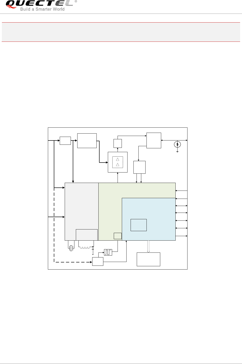
3.2. Pin Assignment
SWD_CLK
SWD_DATA
RESERVED
RESERVED
RESERVED
RESERVED
RESERVED
RESET
RESERVED
1
2
3
4
5
6
10
11
12
13
14
15
16
44
45
46
47
48
51
52
53
54
RESERVED
RESERVED
NETLIGHT
DBG_RXD
DBG_TXD
ADC
RESERVED
RESERVED
RESERVED
RESERVED
VDD_EXT
RESERVED
GPIO3
GPIO2
GPIO1
RESERVED
RI
RESERVED
RESERVED
TXD
RXD
RESERVED
GND
GND
27
26
25
24
23
20
19
18
17
9
8
RESERVED
RESERVED
RESERVED
GND
RESERVED
RESERVED
RESERVED
RESERVED
RESERVED
7
43
42
41
40
39
38
35
36
37
34
33
32
31
30
29
28
21
22
50
49
GND
RF_ANT
GND
GND
RESERVED
VBAT
VBAT
GND
GND
RESERVED
RESERVED
RESERVED
55
56
57
58
59
60
75
76
77
78
79
80
90
89
88
87
86
85
70
69
68
67
66
65
83 84
81 82
63 64
61 62
72 71
74 73
92 91
94 93
POWER ADC UART GPIO OTHERSGND RESERVED
SWD ANT
Figure 2: Pin Assignment

eLTE-IoT Module Series
eLTE-IoT eM300-8a Hardware Design
eLTE-IoT_eM300-8a_Hardware_Design Confidential / Released 16 / 46
3.3. Pin Description
The following tables show the pin definition and description of eM300-8a.
Table 3: I/O Parameters Definition
Type
Description
IO
Bidirectional
DI
Digital input
DO
Digital output
PI
Power input
PO
Power output
AI
Analog input
AO
Analog output
OD
Open drain
Table 4: Pin Description
Power Supply
Pin Name
Pin No.
I/O
Description
DC Characteristics
Comment
VBAT
45, 46
PI
Main power supply of
the module:
VBAT=3.1V~4.2V
Vmax=4.2V
Vmin=3.1V
Vnorm=3.6V
VDD_
EXT
26
PI
Power supply for module
baseband part
Vmax=3.6V
Vmin=1.7V
Vnorm=1.8V or 3.0V
Recommend to add a
2.2~4.7uF bypass
capacitor when
supplying this pin.
GND
2, 42,
43, 47,
48, 51,
52, 54,
59~66,
71~74,
81~83,
92~94
Ground

eLTE-IoT Module Series
eLTE-IoT eM300-8a Hardware Design
eLTE-IoT_eM300-8a_Hardware_Design Confidential / Released 17 / 46
SWD Interface
Pin Name
Pin No.
I/O
Description
DC Characteristics
Comment
SWD_
DATA
3
IO
Serial wire data signal
VOLmax=0.1×VDD_
EXT
VOHmin=0.8×VDD_
EXT
VILmin=-0.1×VDD_
EXT
VILmax=0.2×VDD_
EXT
VIHmin=0.7×VDD_
EXT
VIHmax=1.1×VDD_
EXT
Used for firmware
upgrading.
SWD_
CLK
4
DI
Serial wire clock signal
VOLmax=0.1×VDD_
EXT
VOHmin=0.8×VDD_
EXT
Reset Interface
Pin Name
Pin No.
I/O
Description
DC Characteristics
Comment
RESET
15
DI
Reset the module
RPU≈78kΩ
VIHmax=1.1×VDD_
EXT
VIHmin=0.7×VDD_
EXT
VILmax=0.2×VDD_
EXT
Pull up internally.
Active low.
Network Status Indicator
Pin Name
Pin No.
I/O
Description
DC Characteristics
Comment
NETLIGHT
18
DO
Network status
indication
VOLmax=0.1×VDD_
EXT
VOHmin=0.8×VDD_
EXT
If unused, keep this
pin open.
ADC interface
Pin Name
Pin No.
I/O
Description
DC Characteristics
Comment
ADC
21
AI
General purpose analog
to digital converter
Input voltage range:
0V to VBAT
If unused, keep this
pin open.

eLTE-IoT Module Series
eLTE-IoT eM300-8a Hardware Design
eLTE-IoT_eM300-8a_Hardware_Design Confidential / Released 18 / 46
UART Port
Pin Name
Pin No.
I/O
Description
DC Characteristics
Comment
RXD
29
DI
Receive data
VILmax=0.2×VDD_
EXT
VIHmin=0.7×VDD_
EXT
VIHmax=1.1×VDD_
EXT
VDD_EXT power
domain.
TXD
30
DO
Transmit data
VOLmax=0.1×VDD_
EXT
VOHmin=0.8×VDD_
EXT
VDD_EXT power
domain.
RI
34
DO
Ring indicator
VOLmax=0.1×VDD_
EXT
VOHmin=0.8×VDD_
EXT
VDD_EXT power
domain.
If unused, keep this
pin open.
Debug Port
Pin Name
Pin No.
I/O
Description
DC Characteristics
Comment
DBG_
RXD
19
DI
Receive data
VILmax=0.2×VDD_
EXT
VIHmin=0.7×VDD_
EXT
VIHmax=1.1×VDD_
EXT
If unused, keep these
pins open.
DBG_
TXD
20
DO
Transmit data
VOLmax=0.1×VDD_
EXT
VOHmin=0.8×VDD_
EXT
If unused, keep these
pins open.
GPIO Interfaces
Pin Name
Pin No.
I/O
Description
DC Characteristics
Comment
GPIO1
39
IO
Digital programmable
input/output
VOLmax=0.1×VDD_
EXT
VOHmin=0.8×VDD_
EXT
VILmin=-0.1×VDD_
EXT
VILmax=0.2×VDD_
EXT
VIHmin=0.7×VDD_
EXT
If unused, keep these
pins open.
GPIO2
40
IO
Digital programmable
input/output
GPIO3
41
IO
Digital programmable
input/output

eLTE-IoT Module Series
eLTE-IoT eM300-8a Hardware Design
eLTE-IoT_eM300-8a_Hardware_Design Confidential / Released 19 / 46
3.4. Operating Modes
eM300-8a module has three operating modes, which can determine availability of functions for different
levels of power-saving.
Table 5: Overview of Operating Modes
VIHmax=1.1×VDD_
EXT
RF Interface
Pin Name
Pin No.
I/O
Description
DC Characteristics
Comment
RF_ANT
53
IO
RF antenna pad
Impedance of 50Ω
RESERVED Pins
Pin Name
Pin No.
I/O
Description
DC Characteristics
Comment
RESERVED
1, 5~14,
16, 17,
22, 23,
24, 25,
27, 28,
31~33,
35~38,
44, 49,
50,
55~58,
67~70,
75~80,
84~91
Reserved
Keep these pins
unconnected.
Mode
Function
Normal Operation
Active
In active mode, all functions of the module are available and all
processors are active. Radio transmission and reception can be
performed. Transitions to idle mode and PSM can only be initiated
in Active mode.
Idle
In idle mode, all processors are inactive, but all peripherals can be
active. The system clock is active and power consumption is
reduced via clock gating and power gating. Idle mode is entered

eLTE-IoT Module Series
eLTE-IoT eM300-8a Hardware Design
eLTE-IoT_eM300-8a_Hardware_Design Confidential / Released 20 / 46
3.5. Power Supply
3.5.1. Power Supply Pins
eM300-8a provides two VBAT pins and one VDD_EXT pin dedicated for connection with the external
power supply. The supply voltage of VDD EXT should not be greater than the VBAT voltage.
The following table shows the VBAT, VDD_EXT and ground pins.
Table 6: VBAT, VDD_EXT and GND Pins
Pin Name
Pin No.
Description
Min.
Typ.
Max.
Unit
VBAT
45, 46
Main power supply of the
module
3.1
3.6
4.2
V
VDD_EXT
26
Power supply for module
baseband part
1.7
1.8/3.0
3.6
V
GND
2, 42, 43, 47, 48, 51,
52, 54, 59~66,
71~74, 81~83,
92~94
Ground
-
0
-
V
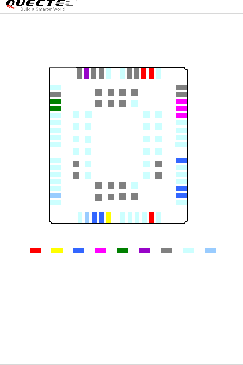
3.5.2. Reference Design for Power Supply
The power design for the module is very important, as the performance of the module largely depends on
the power source. The VBAT power supply is capable of providing the sufficient current up to 0.5A at least.
The VBAT power supply range is from 3.1V to 4.2V and the VDD_EXT supports 1.7V to 3.6V power
supply. Make sure that the input voltage of the VBAT will never drop below 3.1V even in burst
transmission. If the VBAT power voltage drops below 3.1V, the module will be abnormal.
For better power performance, it is recommended to place a 100uF tantalum capacitor with low ESR
(ESR=0.7Ω) and three ceramic capacitors with 100nF, 100pF and 22pF near the VBAT pin. In order to
increase the number of external power supply interfaces, it is better to use an LDO regulator to supply
when all processors are executing a wait-for-interrupt (WFI)
instruction.
PSM
In PSM, only the 32kHz RTC is working, which means the module
can be moved to active mode by an RTC interrupt or by an
external event through the peripherals that are using the RTC.
This mode is entered by all processors setting the “sleep-deep” bit
and then executing a WFI instruction.
eLTE-IoT Module Series
eLTE-IoT eM300-8a Hardware Design
eLTE-IoT_eM300-8a_Hardware_Design Confidential / Released 21 / 46
power for VDD_EXT. It is also recommended to place a ceramic capacitor with 4.7uF near VDD_EXT pin.
The reference circuit is illustrated in the following figure.
The trace width of VBAT and VDD_EXT should be designed as wide as possible. In principle, the longer
the trace is, the wider it will be.
VBAT
C2C1
+C3 C4
GND
100uF 100nF 100pF 22pF
C5
GND
4.7uF
VDD_EXT
LDO
VBAT
Figure 3: Reference Circuit for the VBAT and VDD_EXT Input
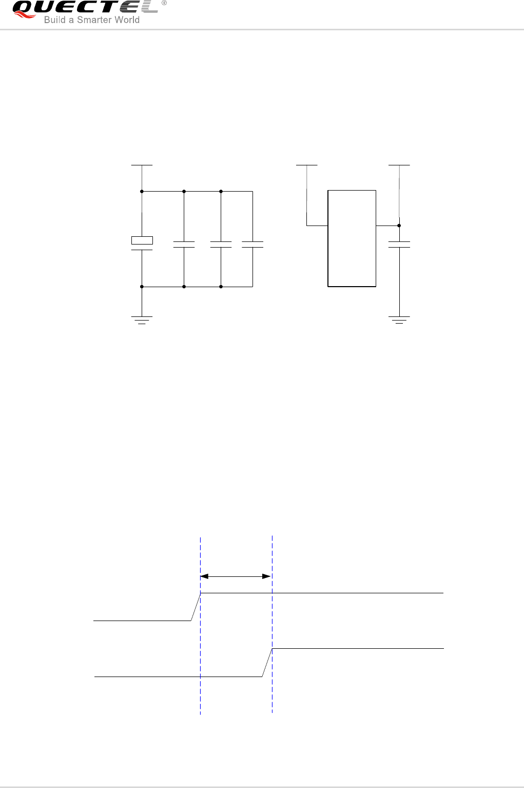
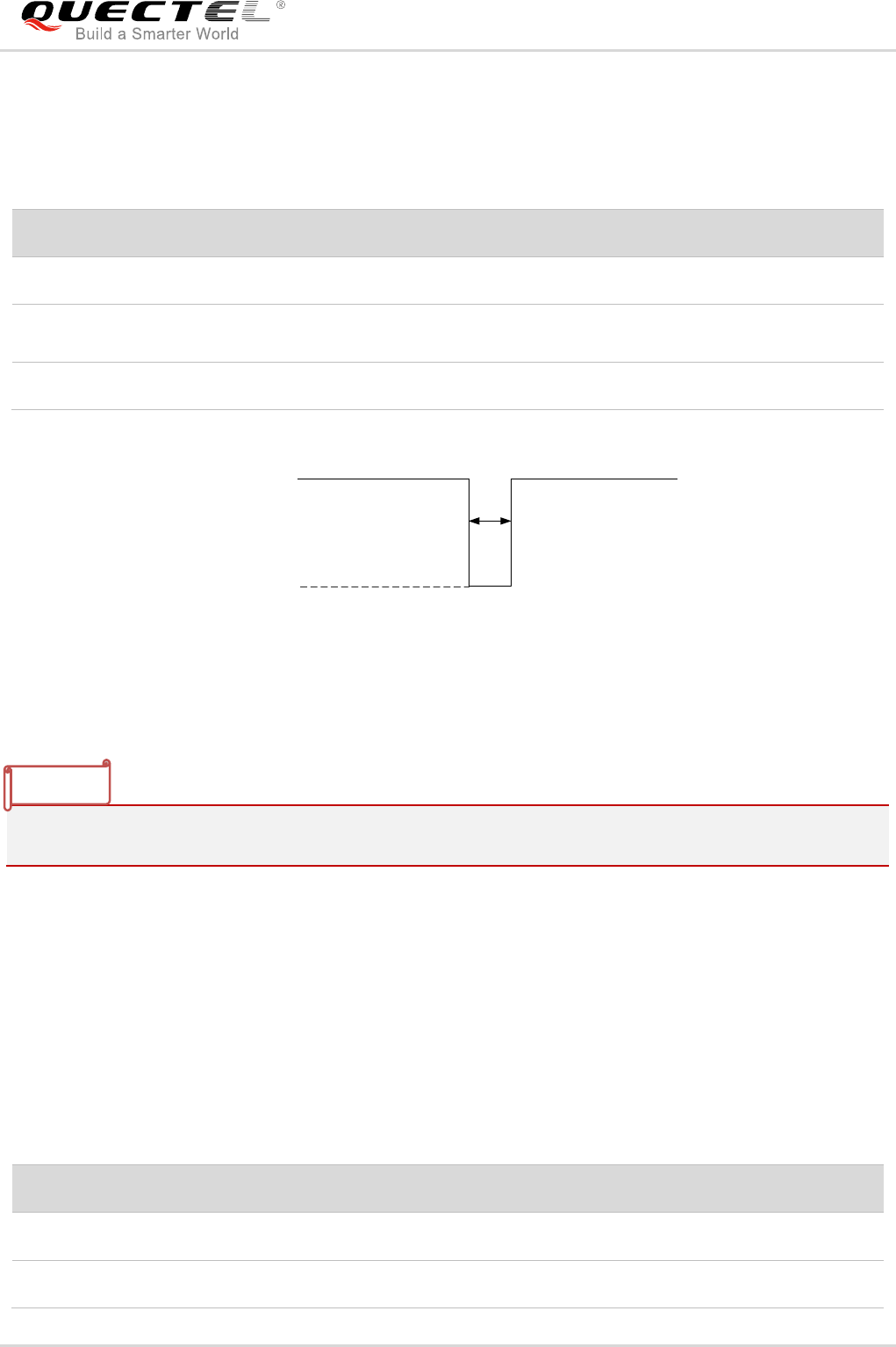
3.6. Power on and down Scenarios
3.6.1. Power on
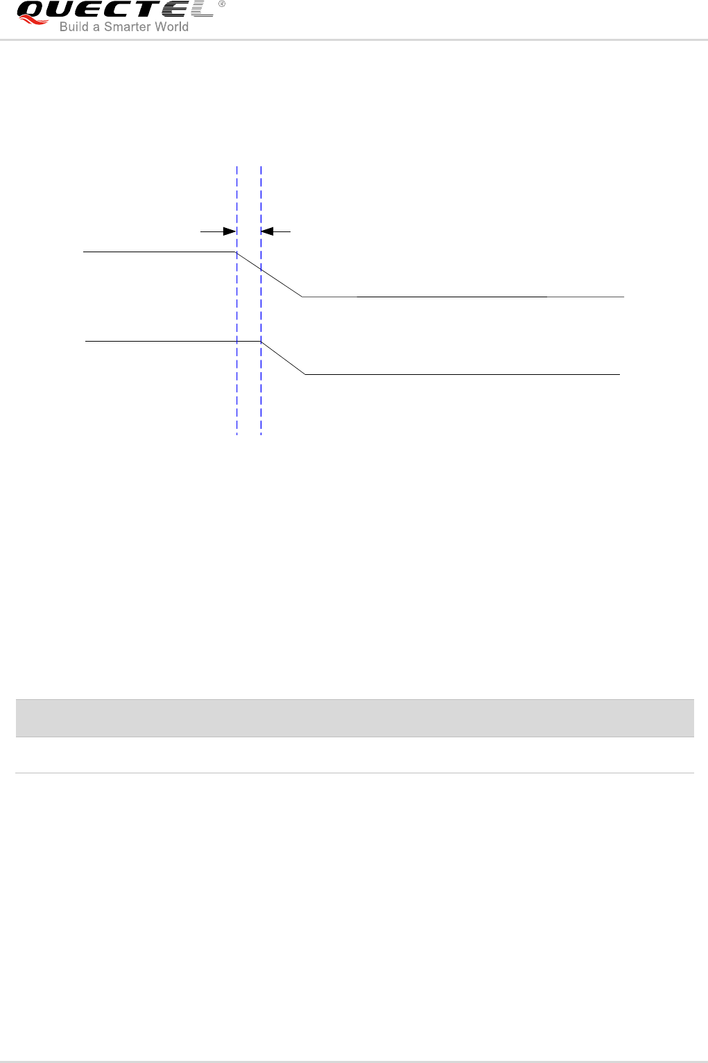
The module can be automatically turned on by supplying power source to VBAT pins.
VBAT
RESET
Delay>535us
Figure 4: Turn-on Timing
eLTE-IoT Module Series
eLTE-IoT eM300-8a Hardware Design
eLTE-IoT_eM300-8a_Hardware_Design Confidential / Released 22 / 46
3.6.2. Power down
The module can be turned off by shutting down the VBAT power supply.
VBAT
RESET
Delay>5ms
Figure 5: Turn-off Timing
3.6.3. Reset the Module
The module can be reset by driving the reset pin to a low level voltage for a certain time. The reset timing
is illustrated as the following table.
Table 7: Reset Characteristics
Pin Name
Pin No.
Description
Reset Time
RESET
15
Reset the module, low active
>100ms
eLTE-IoT Module Series
eLTE-IoT eM300-8a Hardware Design
eLTE-IoT_eM300-8a_Hardware_Design Confidential / Released 23 / 46
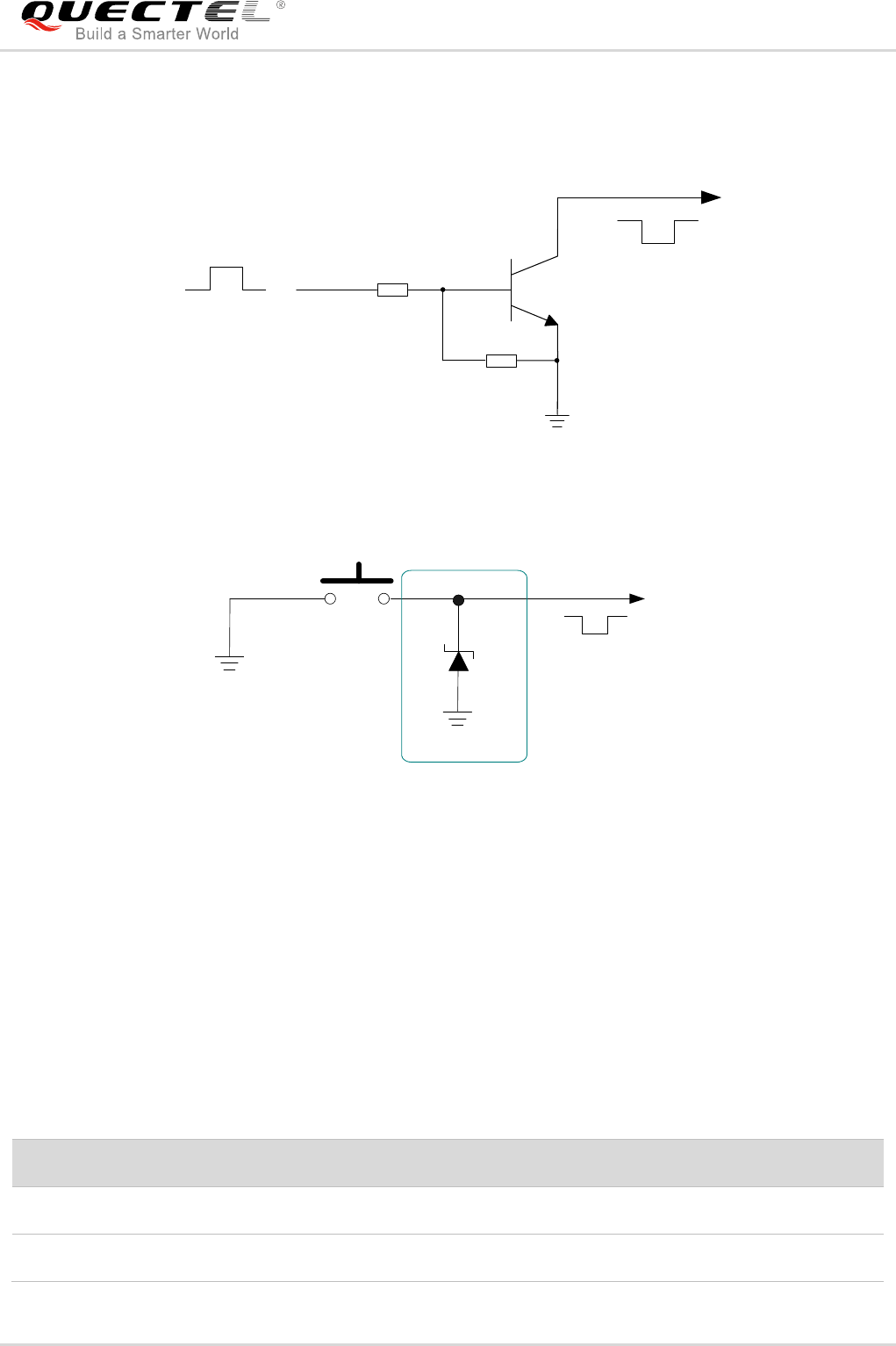
The recommended circuit is shown as below. You can use open drain/collector driver or button to control
the RESET.
Reset pulse
RESET
4.7K
47K
Figure 6: Reference Circuit of RESET by Using Driving Circuit
RESET
S1
Close to S1
TVS
Figure 7: Reference Circuit of RESET by Using Button
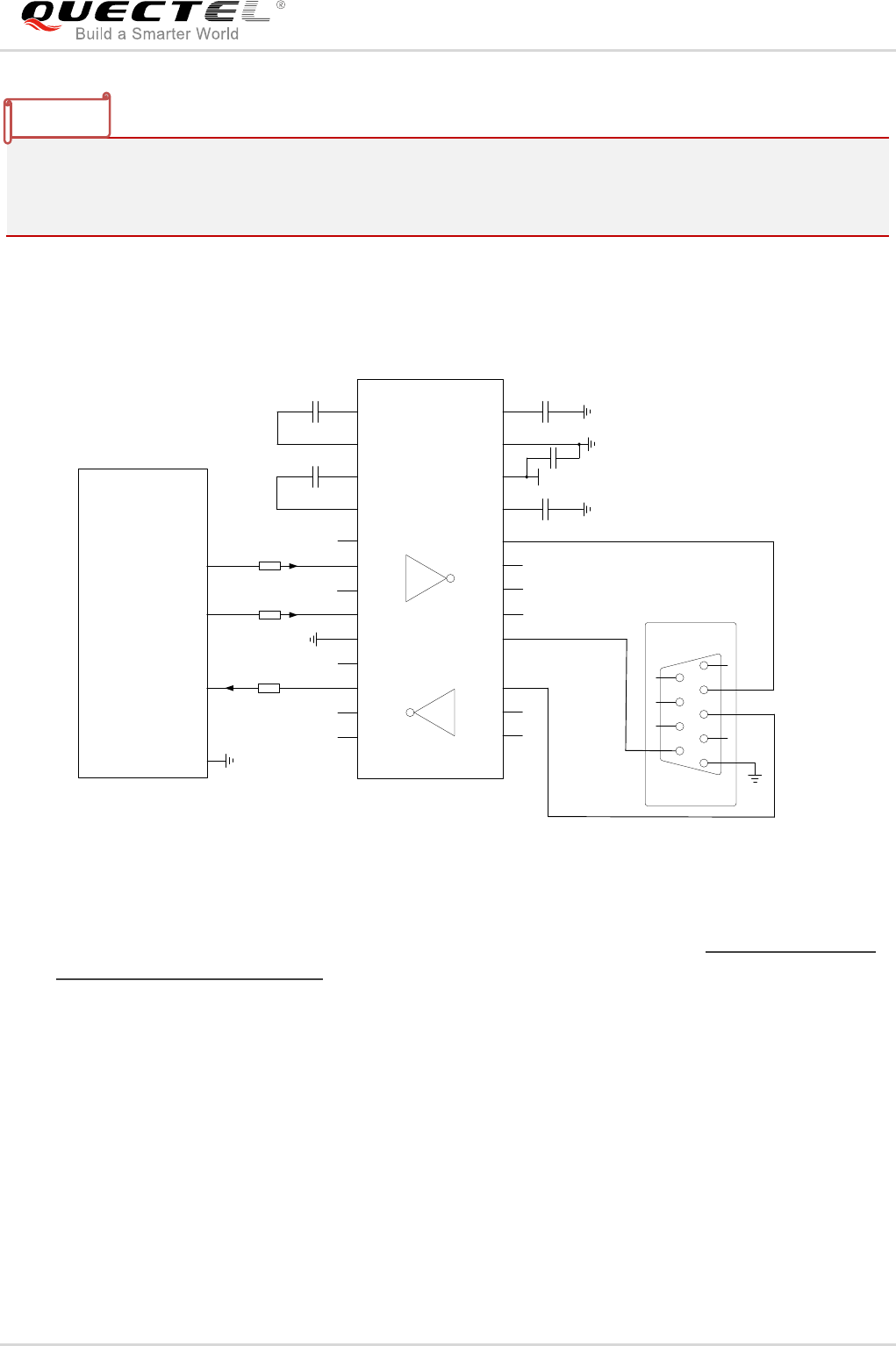
3.7. SWD Interface
The module provides one SWD (Serial Wire Debug) interface for firmware upgrading. It is recommended
to reserve SWD interface in order to upgrade firmware.
Table 8: Pin Definition of SWD Interfaces
Interfaces
Pin Name
Pin No.
Description
SWD
SWD_DATA
3
Serial wire data signal
SWD
SWD_CLK
4
Serial wire clock signal
eLTE-IoT Module Series
eLTE-IoT eM300-8a Hardware Design
eLTE-IoT_eM300-8a_Hardware_Design Confidential / Released 24 / 46
The following figure is a reference design for SWD interface.
VDD_EXT
SWD_CLK
RESET
TDI
Module
(DCE)
GND
RTCK
JTAG_20 PIN
VCC
TRST
TDO
RESET
NC
NC
GND
GND
GND
GND
NC
GND
GND
GND
GND
GND
SWD_DATA SWD_DIO
SWD_CLK
VDD_EXT
Figure 8: Reference Design for SWD Interface
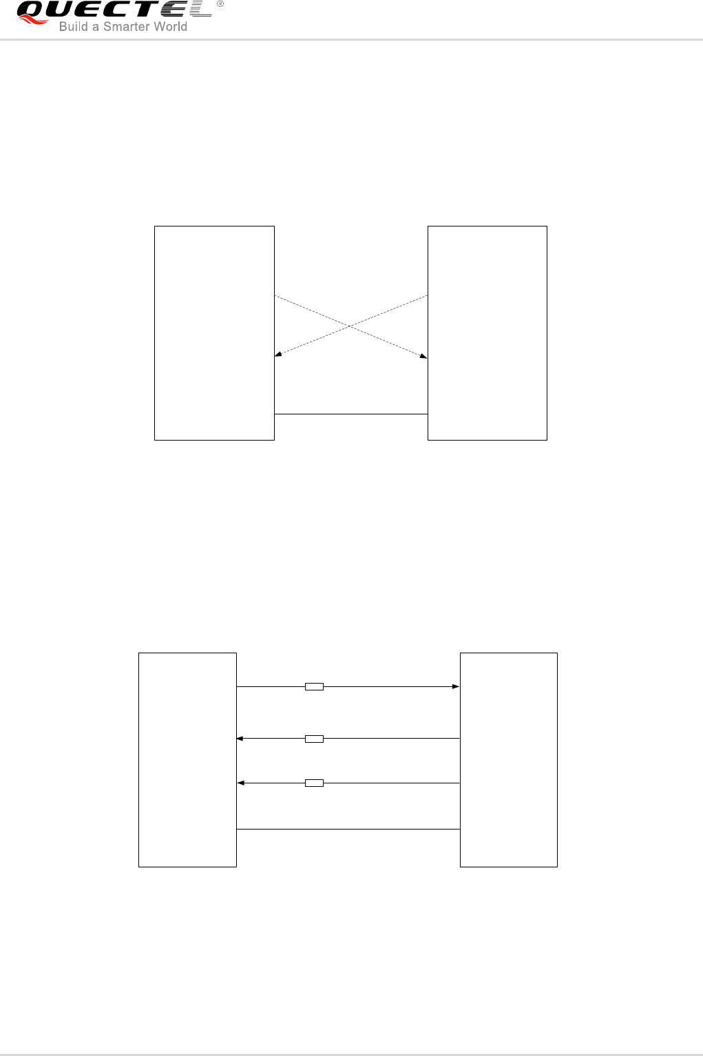
3.8. UART Interfaces
The module provides two UART ports: main port and debug port. The module is designed as a DCE (Data
Communication Equipment), following the traditional DCE-DTE (Data Terminal Equipment) connection.
The main port:
TXD: Send data to RXD of DTE.
RXD: Receive data from TXD of DTE.
RI: Ring indicator (when an SMS is received or data is transmitted, the module will output signals to
inform DTE).
The debug port:
DBG_TXD: Send data to the COM port of computer.
DBG_RXD: Receive data from the COM port of computer.
The logic levels are described in the following table.
Table 9: Pin Definition of the UART Interfaces
Interfaces
Pin No.
Pin Name
Description
Comment
Debug Port
19
DBG_RXD
Receive data
VDD_EXT power
domain
eLTE-IoT Module Series
eLTE-IoT eM300-8a Hardware Design
eLTE-IoT_eM300-8a_Hardware_Design Confidential / Released 25 / 46
Table 10: Logic Levels of the UART Interfaces
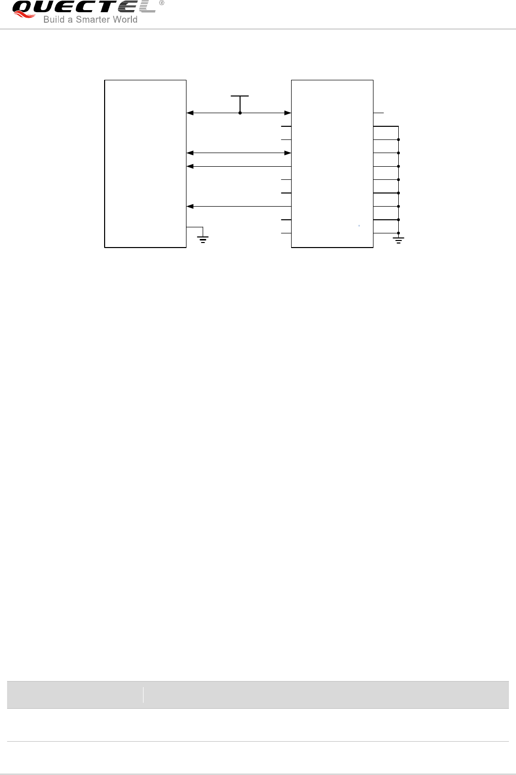
3.8.1. Main Port
Main port can be used for AT command communication and data transmission, and the baud rate is
9600bps. It can also be used for firmware upgrading, and the baud rate is 115200bps.
The following figure shows the connection between the DCE and DTE.
TXD
RXD
RI
TXD
RXD
RING
Module (DCE)
Serial portMain port
GND GND
PC (DTE)
Figure 9: Reference Design for Main Port
20
DBG_TXD
Transmit data
VDD_EXT power
domain
Main Port
29
RXD
Receive data
VDD_EXT power
domain
30
TXD
Transmit data
VDD_EXT power
domain
34
RI
Ring indicator
VDD_EXT power
domain
Parameter
Min.
Max.
Unit
VIL
-0.1×VDD_EXT
0.2×VDD_EXT
V
VIH
0.7×VDD_EXT
1.1×VDD_EXT
V
VOL
0.1×VDD_EXT
V
VOH
0.8×VDD_EXT
VDD_EXT
V
eLTE-IoT Module Series
eLTE-IoT eM300-8a Hardware Design
eLTE-IoT_eM300-8a_Hardware_Design Confidential / Released 26 / 46
3.8.2. Debug Port
Debug port can only be used to view log information with UE Log Viewer tool for debugging. The baud
rate is 57600bps.
A reference design for debug port is shown as below.
DBG_TXD
DBG_RXD
DBG_TXD
DBG_RXD
Module (DCE)
Serial portDebug port
GND GND
PC (DTE)
Figure 10: Reference Design for Debug Port
3.8.3. The UART Application
When the supply voltage of VDD_EXT is 3.0V, the reference design of 3.3V level match is shown as
below.
Peripheral
TXD
RXD
1K
TXD
RXD
RI
EINT
Module
Voltage level: 3.3V
1K
1K
GND GND
Figure 11: Level Match Design for 3.3V System
eLTE-IoT Module Series
eLTE-IoT eM300-8a Hardware Design
eLTE-IoT_eM300-8a_Hardware_Design Confidential / Released 27 / 46
In order to reduce the power consumption of the system, it is highly recommended to add a resistor circuit
on the UART port signal lines when the host‟s voltage level is 3.3V. For systems with a higher voltage
level, a level shifter IC could be used between the host and the module.
The following circuit shows a reference design for the communication between module and PC. As the
electrical level of module is 3.0V, a RS-232 level shifter must be used. Please make sure the I/O voltage
of level shifter which connects to module is 3.0V.
TXD
RXD
RI
Module
GND
C1+
C1-
C2+
C2-
V+
VCC
GND
V-
3.3V
T1IN
T2IN
T3IN
T4IN
R1IN
R2IN
R3IN
R1OUT
R2OUT
R3OUT
T1OUT
T2OUT
T5OUT
T3OUT
T4OUT
T5IN
GND
GND
/R1OUT 1
2
3
4
5
7
8
9
GND
To PC Main Serial Port
GND
1K
1K
1K
RS-232 Level Shifter
6
Figure 12: Sketch Map for RS-232 Interface Match
Please visit vendor web site to select the suitable RS-232 level shifter IC, such as: http://www.exar.com/
and http://www.maximintegrated.com.
3.9. ADC Interface*
The module provides a 10-bit ADC input channel to measure the value of voltage. This ADC is available
in active mode and idle mode.

eLTE-IoT Module Series
eLTE-IoT eM300-8a Hardware Design
eLTE-IoT_eM300-8a_Hardware_Design Confidential / Released 28 / 46
Table 11: Pin Definition of the ADC
“*” means under development.
3.10. GPIO Interface
The module contains three GPIO pins which are controlled through software. The GPIO pins are
controlled by the VDD_EXT power domain.
Table 12: Pin Definition of the GPIO interface
The GPIO pins are available in active, idle and power saving modes. In active and idle modes, data is
sampled and synchronized to the system clock, and interrupts are generated synchronously. In PSM,
data is sampled and synchronized to the RTC clock, and interrupts are generated asynchronously. In all
the three modes, interrupts can be configured to trigger on rising-edge, falling-edge, high-level or
low-level. The GPIO pins can be configured for high drive strength or low drive strength (default) and have
optional pull-down resistors.
Name
Pin No.
Description
ADC
21
Analog to digital converter
Name
Pin No.
Description
GPIO1
39
Digital programmable input/output
GPIO2
40
Digital programmable input/output
GPIO3
41
Digital programmable input/output
eLTE-IoT Module Series
eLTE-IoT eM300-8a Hardware Design
eLTE-IoT_eM300-8a_Hardware_Design Confidential / Released 29 / 46
3.11. Behaviors of the RI*
Table 13: Behaviors of the RI
RI
Idle A URC or
SMS is received
HIGH
LOW
120ms
Figure 13: Behaviors of RI When a URC or SMS is Received
“*” means under development.
3.12. Network Status Indication*
The NETLIGHT signal can be used to drive a network status indicator LED. The working state of this pin
is listed in the following table.
Table 14: Working State of the NETLIGHT
State
RI Response
Idle
HIGH
SMS*
When an SMS is received, the RI is changed to LOW and kept at low level for about
120ms. Then it is changed to HIGH.
URC
Certain URCs can trigger RI to LOW for 120ms. Then it is changed to HIGH.
State
Module Function
Low
The module is not working or not synchronized with network.
High
The module is synchronized with network.
eLTE-IoT Module Series
eLTE-IoT eM300-8a Hardware Design
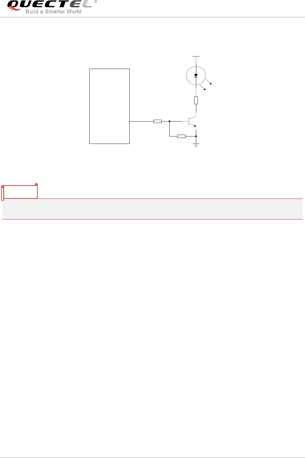
eLTE-IoT_eM300-8a_Hardware_Design Confidential / Released 30 / 46
A reference circuit is shown as below.
Module
NETLIGHT 4.7K
47K
2.2K
VBAT
Figure 14: Reference Design for NETLIGHT
“*” means under development.
eLTE-IoT Module Series
eLTE-IoT eM300-8a Hardware Design
eLTE-IoT_eM300-8a_Hardware_Design Confidential / Released 31 / 46
4 Antenna Interface
The pin 53 is the RF antenna pad. The RF interface has an impedance of 50Ω.
Table 15: Pin Definition of the RF_ANT
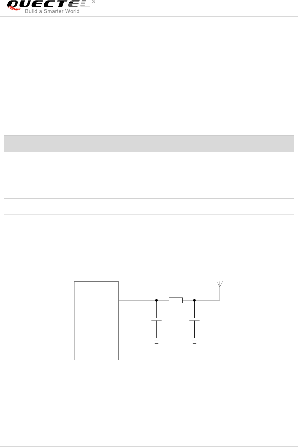
4.1. RF Reference Design
A reference design for RF is shown as below.
Module
RF_ANT
0R
NM NM
Figure 15: Reference Design for RF
eM300-8a provides an RF antenna pad for antenna connection. There is one grounding pad on both
sides of the antenna pad in order to give a better grounding. Besides, a π-type match circuit is suggested
to be used to adjust the RF performance, and place the π-type matching components as close to the
antenna as possible.
Name
Pin
Description
GND
51
Ground
GND
52
Ground
RF_ANT
53
RF antenna pad
GND
54
Ground
eLTE-IoT Module Series
eLTE-IoT eM300-8a Hardware Design
eLTE-IoT_eM300-8a_Hardware_Design Confidential / Released 32 / 46
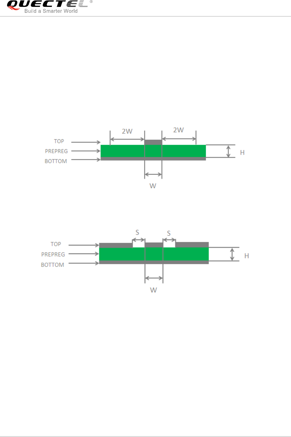
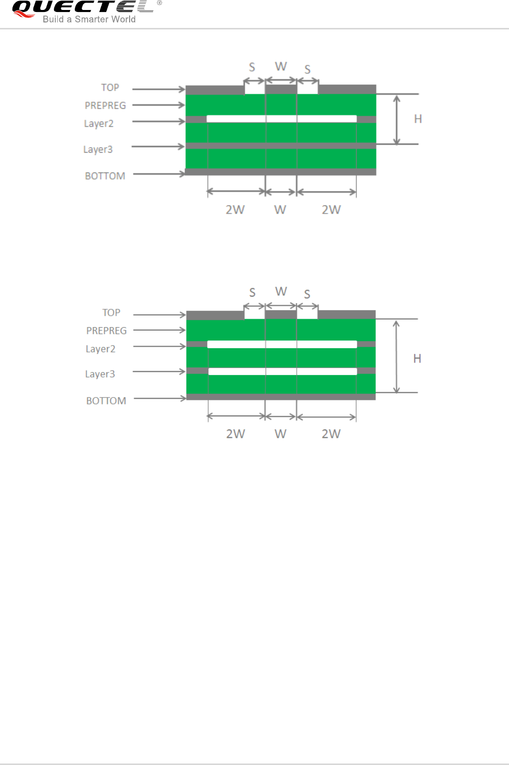
4.2. Reference Design of RF Layout
For user‟s PCB, the characteristic impedance of all RF traces should be controlled as 50 ohm. The
impedance of the RF traces is usually determined by the trace width (W), the materials‟ dielectric constant,
the distance between signal layer and reference ground (H), and the clearance between RF trace and
ground (S). Microstrip line or coplanar waveguide line is typically used in RF layout for characteristic
impedance control. The following are reference designs of microstrip line or coplanar waveguide line with
different PCB structures.
Figure 16: Microstrip Line Design on a 2-layer PCB
Figure 17: Coplanar Waveguide Line Design on a 2-layer PCB
eLTE-IoT Module Series
eLTE-IoT eM300-8a Hardware Design
eLTE-IoT_eM300-8a_Hardware_Design Confidential / Released 33 / 46
Figure 18: Coplanar Waveguide Line Design on a 4-layer PCB (Layer 3 as Reference Ground)
Figure 19: Coplanar Waveguide Line Design on a 4-layer PCB (Layer 4 as Reference Ground)
In order to ensure RF performance and reliability, the following principles should be complied with in RF
layout design:
Use impedance simulation tool to control the characteristic impedance of RF traces as 50 ohm.
The GND pins adjacent to RF pins should not be hot welded, and should be fully connected to
ground.
The distance between the RF pins and the RF connector should be as short as possible, and all the
right angle traces should be changed to curved ones.
There should be clearance area under the signal pin of the antenna connector or solder joint.
The reference ground of RF traces should be complete. Meanwhile, adding some ground vias around
RF traces and the reference ground could help to improve RF performance. The distance between
the ground vias and RF traces should be no less than two times the width of RF signal traces (2*W).
For more details about RF layout, please refer to document [2].

eLTE-IoT Module Series
eLTE-IoT eM300-8a Hardware Design
eLTE-IoT_eM300-8a_Hardware_Design Confidential / Released 34 / 46
4.3. RF Receiving Sensitivity
Table 16: RF Receiving Sensitivity (MCS-1, BLER <10%)
4.4. Antenna Requirement
The following table shows the requirement on eLTE-IoT antenna.
Table 17: Antenna Cable Requirement
Frequency Range
Requirement
863-928MHz
Insertion Loss: <1dB
Table 18: Antenna Requirements
Type
Requirements
Frequency Range
863-928MHz
VSWR
≤2
Gain (dBi)
≤4
Max Input Power (W)
5
Input Impedance (Ω)
50
Polarization Type
linear
Frequency
Receive Sensitivity
902~928MHz
-140dBm
863~870MHz
-140dBm
eLTE-IoT Module Series
eLTE-IoT eM300-8a Hardware Design
eLTE-IoT_eM300-8a_Hardware_Design Confidential / Released 35 / 46
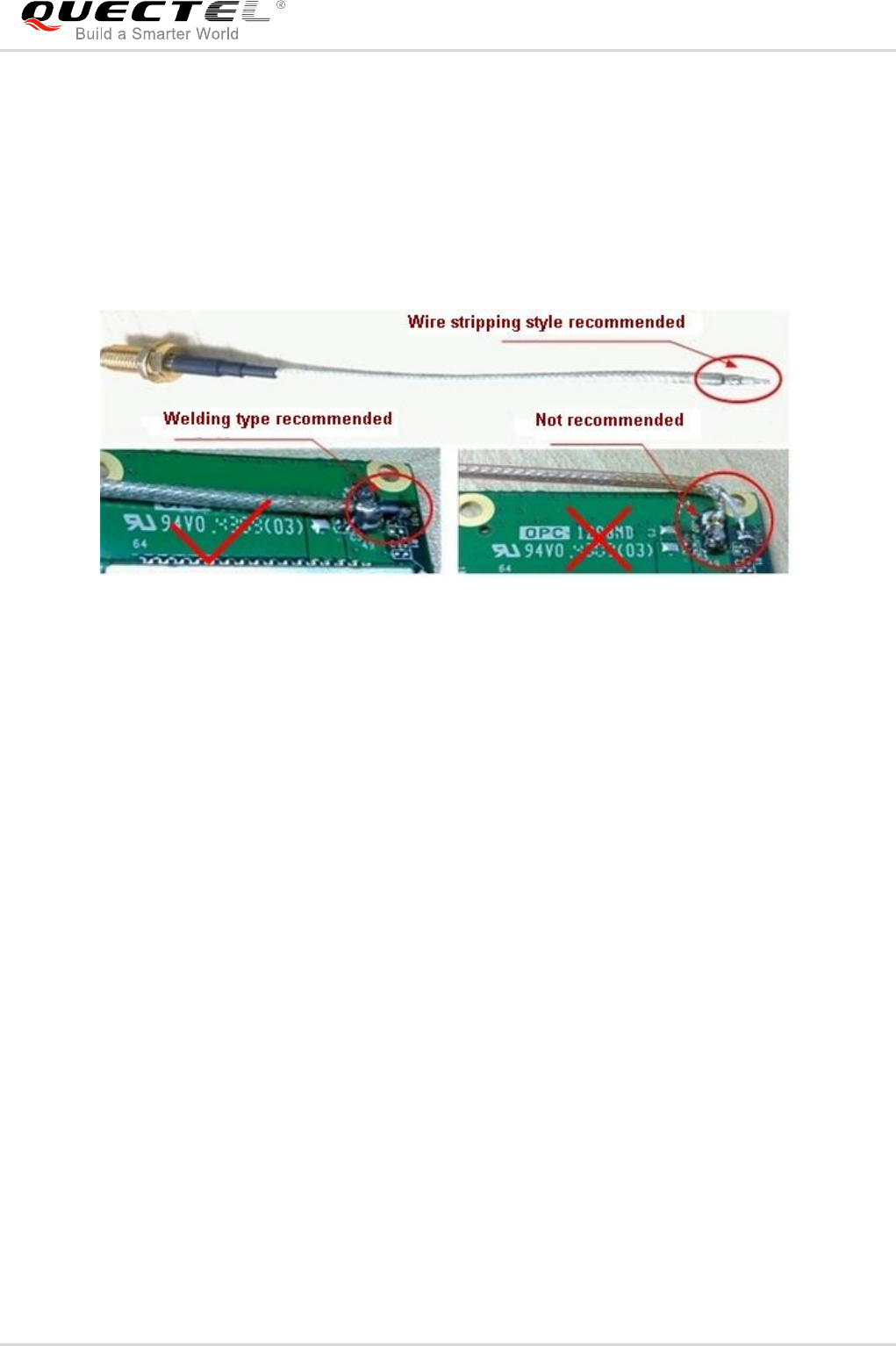
4.5. RF Cable Welding
Welding the RF cable to RF pad of module correctly will reduce the loss on the path of RF, please refer to
the following example of RF cable welding.
Figure 20: Recommended RF Cable Welding

eLTE-IoT Module Series
eLTE-IoT eM300-8a Hardware Design
eLTE-IoT_eM300-8a_Hardware_Design Confidential / Released 36 / 46
5 Electrical, Reliability and Radio
Characteristics
5.1. Absolute Maximum Ratings
Absolute maximum ratings for power supply and voltage on digital and analog pins of the module are
listed in the following table.
Table 19: Absolute Maximum Ratings
Parameter
Min.
Max.
Unit
VBAT
-0.3
+4.2
V
VDD_EXT
-0.3
+3.6
V
Current of Power Supply
0
0.3
A
Voltage at Digital Pins
-0.3
+3.3
V
Voltage at Analog Pins
-0.3
+4.2
V
Voltage at Digital/Analog Pins in Power Down Mode
-0.25
+0.25
V
eLTE-IoT Module Series
eLTE-IoT eM300-8a Hardware Design
eLTE-IoT_eM300-8a_Hardware_Design Confidential / Released 37 / 46
5.2. Operating Temperature
The operating temperature is listed in the following table:
Table 20: Operating Temperature
1. 1) Within operation temperature range, the module is 3GPP compliant.
2. 2) Within extended temperature range, the module remains the ability to establish and maintain an
SMS, data transmission, etc. There is no unrecoverable malfunction; there are also no effects on
radio spectrum and no harm to radio network. Only one or more parameters like Pout might reduce in
their value and exceed the specified tolerances. When the temperature returns to the normal
operating temperature levels, the module will meet 3GPP specifications again.
5.3. Current Consumption
The values of current consumption are shown below.
Table 21: Current Consumption
Parameter
Description
Conditions
Min.
Typ.
Max.
Unit
IVBAT
PSM
Deep sleep state
-
-
-
uA
Idle mode
Standby state
6
mA
Active mode
Radio transmission (23dBm)
250
mA
Radio reception
86
mA
Parameter
Min.
Typ.
Max.
Unit
Operation Temperature Range1)
-30
+25
+75
ºC
Extended Operation Range2)
-40
+85
ºC
eLTE-IoT Module Series
eLTE-IoT eM300-8a Hardware Design
eLTE-IoT_eM300-8a_Hardware_Design Confidential / Released 38 / 46
6 Mechanical Dimensions
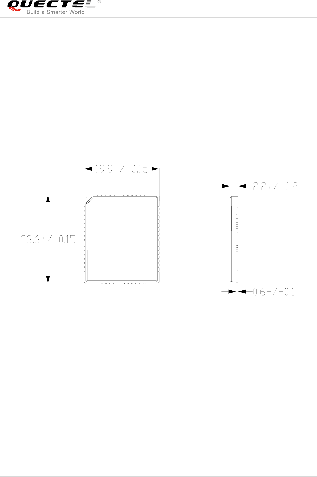
This chapter describes the mechanical dimensions of the module.
6.1. Mechanical Dimensions of the Module
Figure 21: Top and Side Dimensions of eM300-8a Module (Unit: mm)
eLTE-IoT Module Series
eLTE-IoT eM300-8a Hardware Design
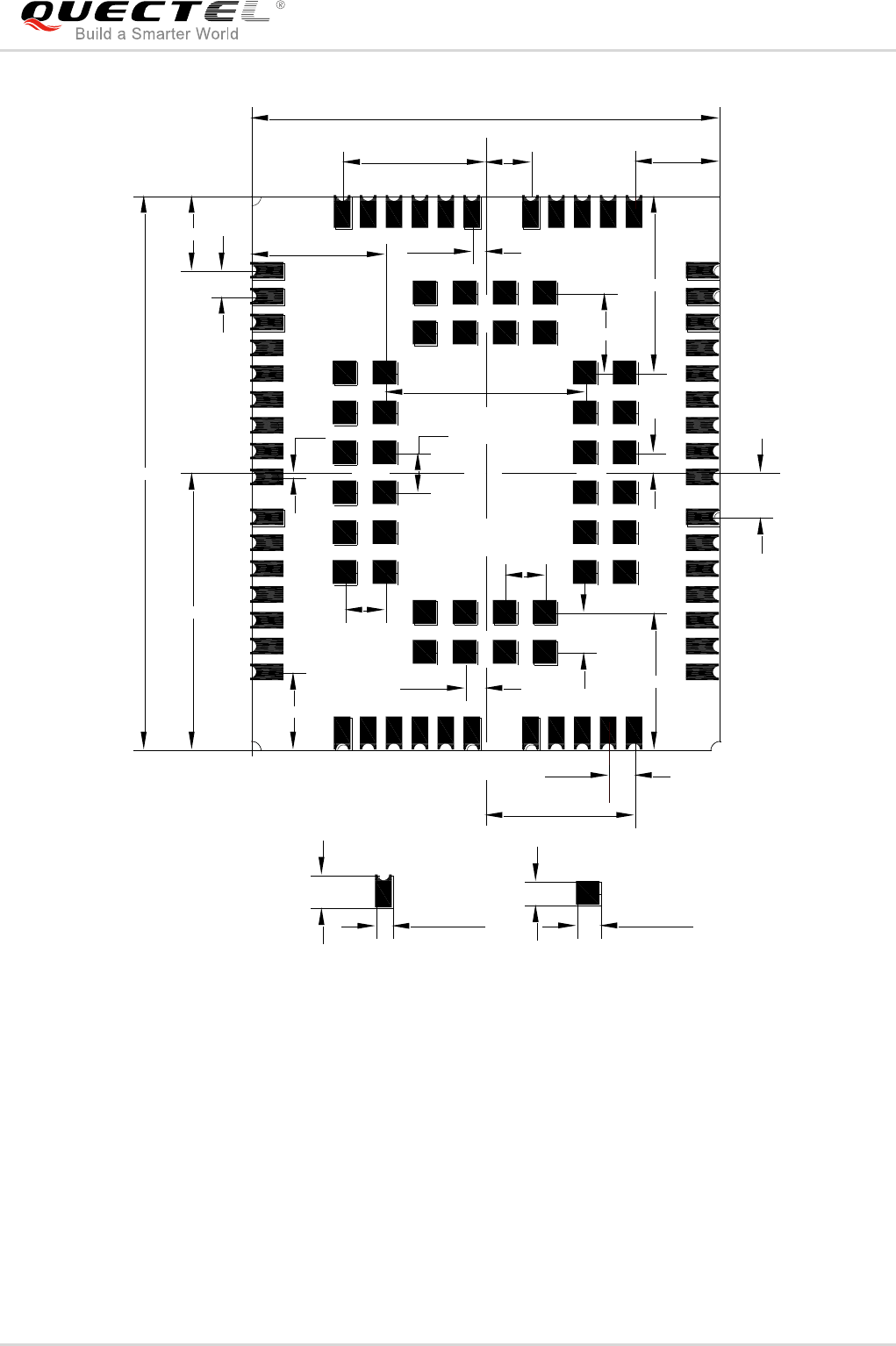
eLTE-IoT_eM300-8a_Hardware_Design Confidential / Released 39 / 46
0.85
1.90
0.20
1.95
0.85
23.60
1.70
1.70
1.70
7.55
11.80
1.10
5.70
8.50
19.90
3.30
5.85
3.40
1.70
3.20 0.55
3.60
6.05
1.10
6.35
40x1.00
40x1.00
54x0.70
54x1.40
1
Figure 22: Bottom Dimensions of eM300-8a Module (Unit: mm)
eLTE-IoT Module Series
eLTE-IoT eM300-8a Hardware Design
eLTE-IoT_eM300-8a_Hardware_Design Confidential / Released 40 / 46
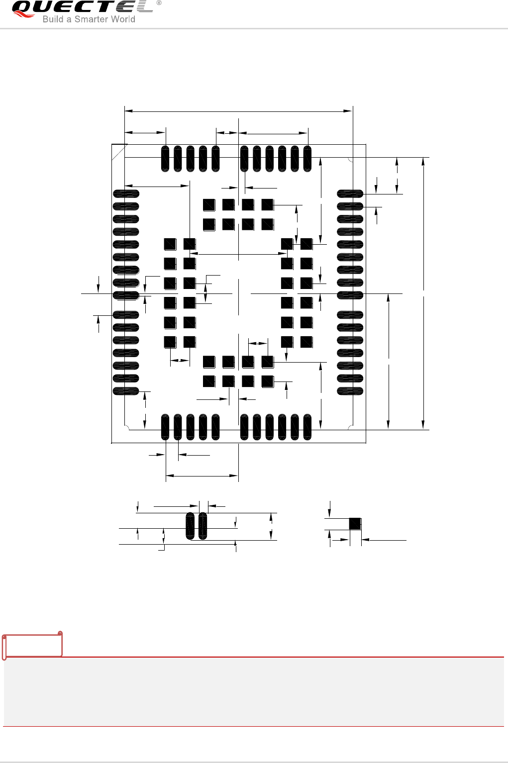
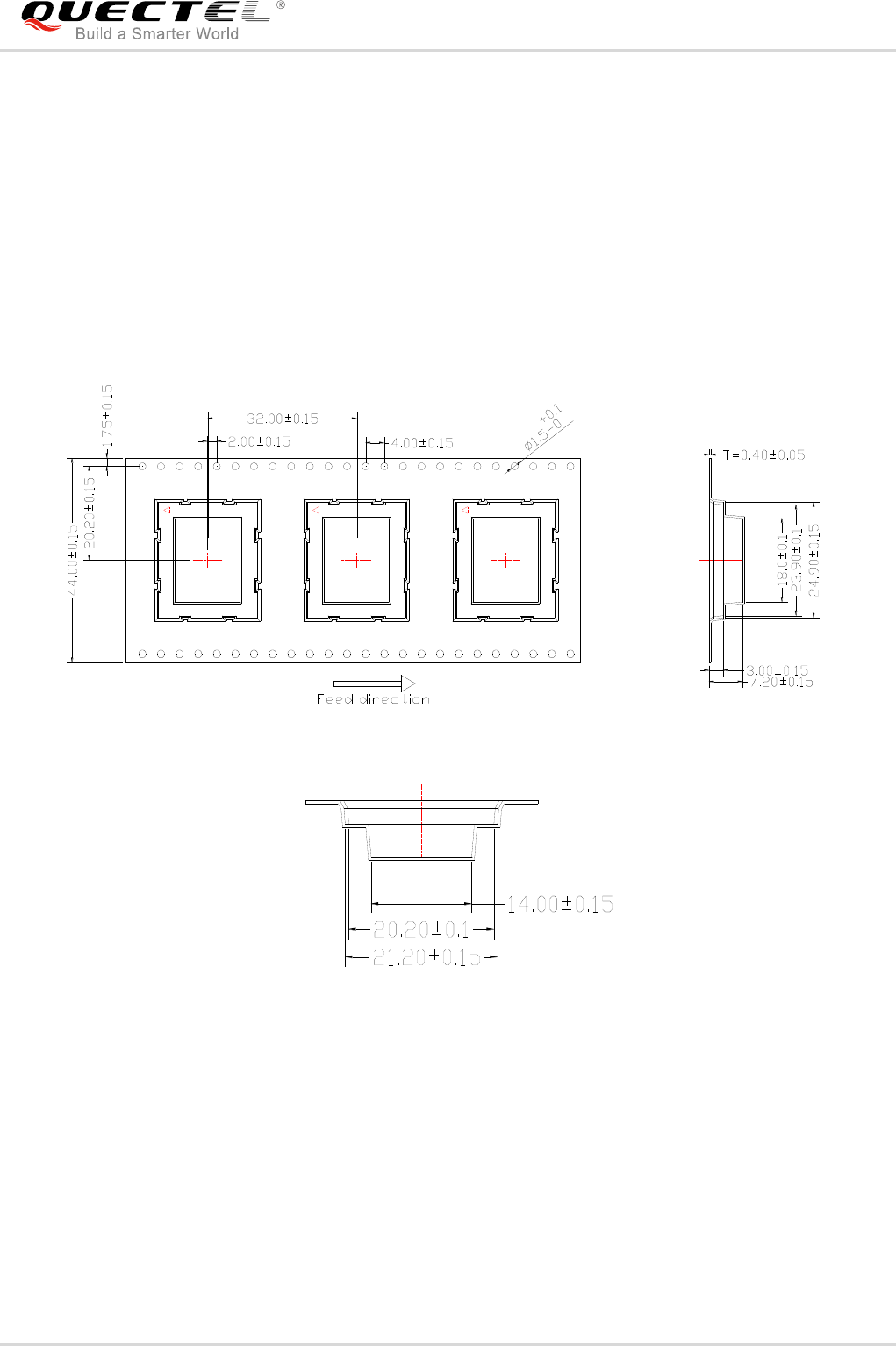
6.2. Recommended Footprint
0.85
1.90
0.20
0.55
1.95
0.85
1.35
1.05
1.5
Frame line
Silksreen
54x2.4
23.60
1.70
1.70
1.70
7.55
11.80
1.10
6.05
5.70
8.50
19.90
1.10
6.35
3.30
5.85
3.60
3.40
54x0.75
1.70
3.20
40x1.00
40x1.00
1
Figure 23: Recommended Footprint (Unit: mm)
1. For easy maintenance of the module, please keep about 3mm between the module and other
components in the host PCB.
2. All RESERVED pins must not be connected to GND.
3. All dimensions are in millimeters.

eLTE-IoT Module Series
eLTE-IoT eM300-8a Hardware Design
eLTE-IoT_eM300-8a_Hardware_Design Confidential / Released 41 / 46
7 Storage, Manufacturing and
Packaging
7.1. Storage
eM300-8a module is stored in a vacuum-sealed bag. The storage restrictions are shown as below.
1. Shelf life in the vacuum-sealed bag: 12 months at <40ºC /90%RH.
2. After the vacuum-sealed bag is opened, devices that will be subjected to reflow soldering or other
high temperature processes must be:
Mounted within 72 hours at the factory environment of ≤30ºC /60% RH.
Stored at <10% RH.
3. Devices require baking before mounting, if any circumstance below occurs:
When the ambient temperature is 23ºC ±5 ºC , humidity indication card shows the humidity is >10%
before opening the vacuum-sealed bag.
Device mounting cannot be finished within 72 hours at factory conditions of ≤30ºC /60%
4. If baking is required, devices may be baked for 48 hours at 125ºC ±5 ºC .
As the plastic container cannot be subjected to high temperature, it should be removed from devices
before high temperature (125ºC ) baking. If shorter baking time is desired, please refer to the
IPC/JEDECJ-STD-033 for baking procedure.
eLTE-IoT Module Series
eLTE-IoT eM300-8a Hardware Design
eLTE-IoT_eM300-8a_Hardware_Design Confidential / Released 42 / 46
7.2. Manufacturing and Soldering
Push the squeegee to apply the solder paste on the surface of stencil, thus making the paste fill the
stencil openings and then penetrate to the PCB. The force on the squeegee should be adjusted properly
so as to produce a clean stencil surface on a single pass. To ensure the module soldering quality, the
thickness of stencil for the pads at the bottom of the module should be 0.15mm. For more details, please
refer to document [1].
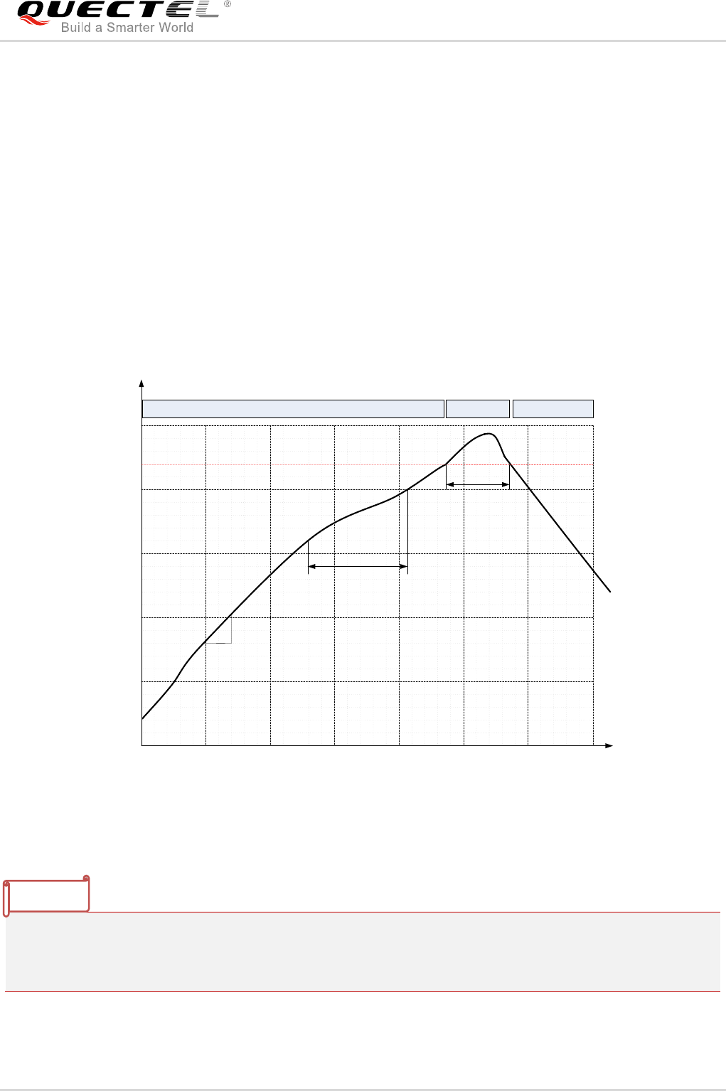
It is suggested that the peak reflow temperature is 235 ~ 245ºC (for SnAg3.0Cu0.5 alloy). The absolute
max reflow temperature is 260ºC. To avoid damage to the module when it is repeatedly heated, it is
suggested that the module should be mounted after reflow soldering for the other side of PCB has been
completed. Recommended reflow soldering thermal profile is shown below.
Time
50 100 150 200 250 300
50
100
150
200
250
160ºC
200ºC
217
0
70s~120s
40s~60s
Between 1~3ºC/s
Preheat Heating Cooling
ºC
s
Liquids Temperature
Temperature
Figure 24: Reflow Soldering Thermal Profile
During manufacturing and soldering, or any other processes that may contact the module directly, NEVER
wipe the module label with organic solvents, such as acetone, ethyl alcohol, isopropyl alcohol,
trichloroethylene, etc.
eLTE-IoT Module Series
eLTE-IoT eM300-8a Hardware Design
eLTE-IoT_eM300-8a_Hardware_Design Confidential / Released 43 / 46
7.3. Packaging
The modules are stored inside a vacuum-sealed bag which is ESD protected. It should not be opened
until the devices are ready to be soldered onto the application.
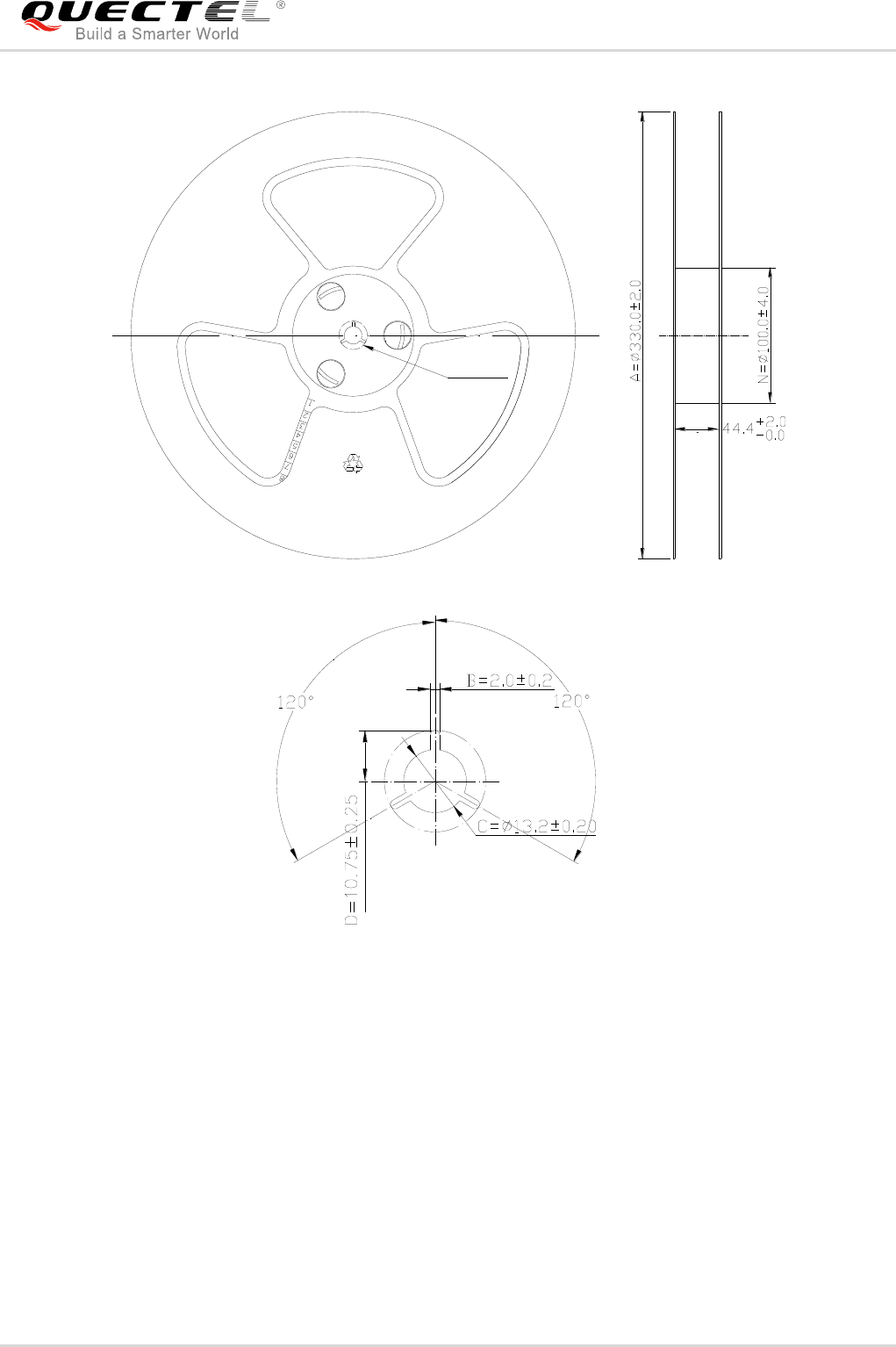
7.3.1. Tape and Reel Packaging
The reel is 330mm in diameter and each reel contains 250 modules.
Figure 25: Tape Dimensions
eLTE-IoT Module Series
eLTE-IoT eM300-8a Hardware Design
eLTE-IoT_eM300-8a_Hardware_Design Confidential / Released 44 / 46
PS
6
DETAIL:A
DETAIL:A
Figure 26: Reel Dimensions

eLTE-IoT Module Series
eLTE-IoT eM300-8a Hardware Design
eLTE-IoT_eM300-8a_Hardware_Design Confidential / Released 45 / 46
8 Appendix A Reference
Table 22: Related Documents
Table 23: Terms and Abbreviations
SN
Document Name
Remark
[1]
Quectel_Module_Secondary_SMT_User_Guide
Module Secondary SMT User Guide
[2]
Quectel_RF_Layout_Application_Note
RF Layout Application Note
Abbreviation
Description
ADC
Analog-to-Digital Converter
DCE
Data Communications Equipment (typically module)
DTE
Data Terminal Equipment (typically computer, external controller)
eLTE-IoT
Evolved Long Term Evolution Internet of Things
I/O
Input/Output
IC
Integrated Circuit
Imax
Maximum Load Current
Inorm
Normal Current
kbps
Kilo Bits Per Second
LED
Light Emitting Diode
PCB
Printed Circuit Board
PSM
Power Saving Mode
RF
Radio Frequency

eLTE-IoT Module Series
eLTE-IoT eM300-8a Hardware Design
eLTE-IoT_eM300-8a_Hardware_Design Confidential / Released 46 / 46
RMS
Root Mean Square (value)
RoHS
Restriction of Hazardous Substances
RTC
Real Time Clock
RX
Receive Direction
USIM
Universal Subscriber Identification Module
SMS
Short Message Service
TE
Terminal Equipment
TX
Transmitting Direction
UART
Universal Asynchronous Receiver & Transmitter
URC
Unsolicited Result Code
VSWR
Voltage Standing Wave Ratio
Vmax
Maximum Voltage Value
Vnorm
Normal Voltage Value
Vmin
Minimum Voltage Value
VIHmax
Maximum Input High Level Voltage Value
VIHmin
Minimum Input High Level Voltage Value
VILmax
Maximum Input Low Level Voltage Value
VILmin
Minimum Input Low Level Voltage Value
VImax
Absolute Maximum Input Voltage Value
VImin
Absolute Minimum Input Voltage Value
VOHmax
Maximum Output High Level Voltage Value
VOHmin
Minimum Output High Level Voltage Value
VOLmax
Maximum Output Low Level Voltage Value
VOLmin
Minimum Output Low Level Voltage Value