Huawei Technologies MC703 Wireless Module supporting CDMA/EvDO 800/1900 User Manual MC703 Product Description
Huawei Technologies Co.,Ltd Wireless Module supporting CDMA/EvDO 800/1900 MC703 Product Description
Contents
- 1. User Manual 1
- 2. User Manual 2
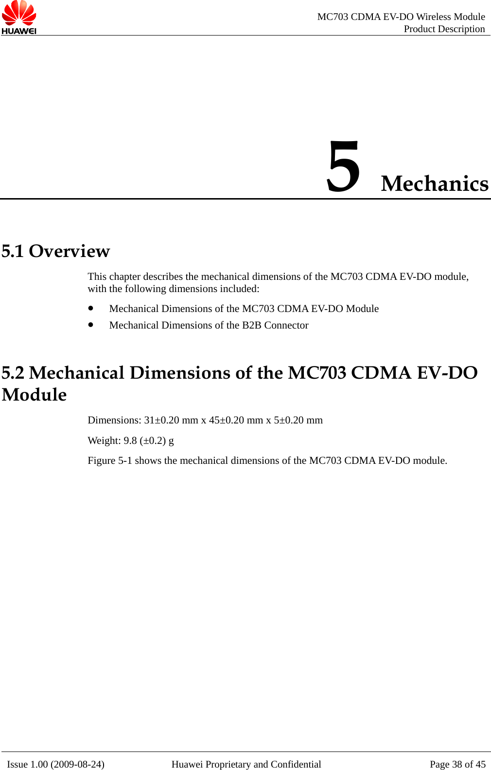
User Manual 2