Huawei Technologies MC703 Wireless Module supporting CDMA/EvDO 800/1900 User Manual MC703 Product Description
Huawei Technologies Co.,Ltd Wireless Module supporting CDMA/EvDO 800/1900 MC703 Product Description
Contents
- 1. User Manual 1
- 2. User Manual 2
User Manual 2

Product Description
MC703 CDMA EV-DO Wireless Module
V100R001
Issue 1.00
Date 2009-08-24
HUAWEI TECHNOLOGIES CO., LTD.

Huawei Technologies Co., Ltd. provides customers with comprehensive technical support and service.
Please feel free to contact our local office or company headquarters.
Huawei Technologies Co., Ltd.
Address: Huawei Industrial Base
Bantian, Longgang
Shenzhen 518129
People's Republic of China
Website: http://www.huawei.com
Email: support@huawei.com
Copyright © Huawei Technologies Co., Ltd. 2009. All rights reserved.
No part of this document may be reproduced or transmitted in any form or by any means without prior
written consent of Huawei Technologies Co., Ltd.
Trademarks and Permissions
and other Huawei trademarks are trademarks of Huawei Technologies Co., Ltd. All other trademarks
and trade names mentioned in this document are the property of their respective holders.
Notice
The information in this document is subject to change without notice. Every effort has been made in the
preparation of this document to ensure accuracy of the contents, but all statements, information, and
recommendations in this document do not constitute the warranty of any kind, express or implied.
Issue 1.00 (2009-08-24) Huawei Proprietary and Confidential Page 2 of 45
MC703 CDMA EV-DO Wireless Module
Product Description
Issue 1.00 (2009-08-24) Huawei Proprietary and Confidential Page 3 of 45
About This Document
History
Issue Details Date Author Approved by
V1.00 Initial formal release. 2009-8-24 Zhang Jun zhou Zhaoxing

MC703 CDMA EV-DO Wireless Module
Product Description
Issue 1.00 (2009-08-24) Huawei Proprietary and Confidential Page 4 of 45
Contents
1 Product Overview .........................................................................................................................9
1.1 About This Chapter ..........................................................................................................................................9
1.2 Functions of the MC703 CDMA EV-DO Module............................................................................................9
1.3 Application Block Diagram of the MC703 CDMA EV-DO Module ............................................................. 11
2 Interface Description..................................................................................................................12
2.1 About This Chapter ........................................................................................................................................12
2.2 Signal Connector Interface.............................................................................................................................12
2.2.1 Interface Signals....................................................................................................................................12
2.3 Antenna Interfaces..........................................................................................................................................15
2.3.1 Antenna Interface Circuits ....................................................................................................................15
3 Electrical Features of the Interfaces.........................................................................................18
3.1 About This Chapter ........................................................................................................................................18
3.2 Application Extremes.....................................................................................................................................18
3.3 Operating and Storage Temperature...............................................................................................................19
3.4 Levels of the I/O Interface .............................................................................................................................19
3.5 Power Supply Features...................................................................................................................................19
3.5.1 Input Power Supply...............................................................................................................................19
3.5.2 Operating Current .................................................................................................................................20
3.5.3 Power-on, Power-off, and Reset Processes...........................................................................................21
3.5.4 RTC Power Supply ...............................................................................................................................23
3.6 Reliability Features ........................................................................................................................................24
3.7 ESD Features..................................................................................................................................................25
3.7.1 Overview...............................................................................................................................................25
3.7.2 ESD Protection on the Antenna Interface .............................................................................................25
3.7.3 ESD Protection on the RUIM Card Interface........................................................................................25
4 Interface Applications................................................................................................................27
4.1 About This Chapter ........................................................................................................................................27
4.2 UART Interface..............................................................................................................................................27
4.3 RUIM Card Interface .....................................................................................................................................30
4.4 Audio Interfaces .............................................................................................................................................32
4.5 Power Supply Interface.................................................................................................................................. 33
4.6 USB Bus.........................................................................................................................................................34

MC703 CDMA EV-DO Wireless Module
Product Description
Issue 1.00 (2009-08-24) Huawei Proprietary and Confidential Page 5 of 45
4.7 GPIO Interface ...............................................................................................................................................34
4.8 ADC Interfaces...............................................................................................................................................35
4.9 Status Indication Pins.....................................................................................................................................35
4.9.1 LED Circuits......................................................................................................................................... 35
4.10 Pin Sequence................................................................................................................................................37
5 Mechanics .....................................................................................................................................38
5.1 Overview........................................................................................................................................................38
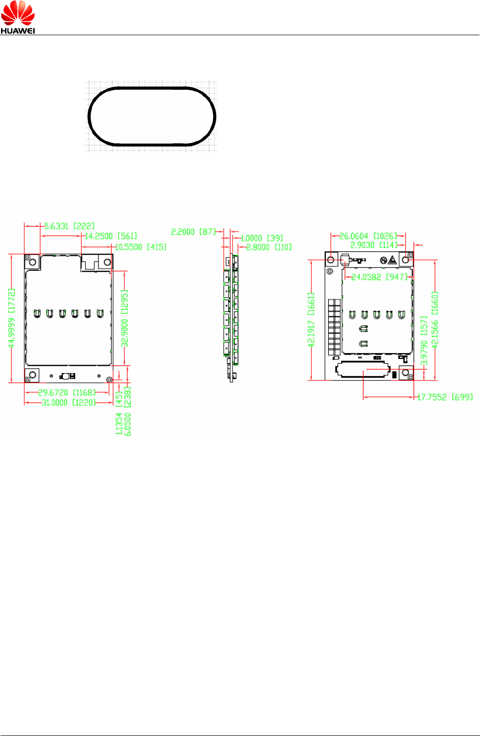
5.2 Mechanical Dimensions of the MC703 CDMA EV-DO Module...................................................................38
5.3 Mechanical Dimensions of the B2B Connector.............................................................................................40
A Acronyms and Abbreviations..................................................................................................44

MC703 CDMA EV-DO Wireless Module
Product Description
Issue 1.00 (2009-08-24) Huawei Proprietary and Confidential Page 6 of 45
Figures
Figure 1-1 Application block diagram of the MC703 CDMA EV-DO module................................................... 11
Figure 2-1 Dimensions of the RF connector........................................................................................................16
Figure 2-2 RF connector......................................................................................................................................17
Figure 3-1 Power-on process of the MC703 CDMA EV-DO module.................................................................21
Figure 3-2 Normal power-off process of the MC703 CDMA EV-DO module....................................................22
Figure 3-3 Reset process of the MC703 CDMA EV-DO module........................................................................23
Figure 3-4 Recommended circuit for the ESD protection on the antenna interface............................................25
Figure 3-5 Recommended circuit for ESD protection on the RUIM card interface............................................25
Figure 4-1 Connections between the DCE and DTE........................................................................................... 28
Figure 4-2 Connections between the serial interface and the 3 V single-chip microcontroller ...........................29
Figure 4-3 Connections for the 3-wire serial interface........................................................................................29
Figure 4-4 Electrical connections for the 9-wire serial interface with the flow control function........................30
Figure 4-5 Circuits of the RUIM card interface .................................................................................................. 31
Figure 4-6 Sequence of the pins of the RUIM card.............................................................................................31
Figure 4-7 Sequence of the pins of a RUIM card seat.........................................................................................31
Figure 4-8 Circuits of the first audio interface ....................................................................................................33
Figure 4-9 Connections between the MC703 CDMA EV-DO module and the 8-ohm speaker...........................33
Figure 4-10 Reference circuits for the design of the LDO power supply............................................................34
Figure 4-11 Reference circuits of the design of the ADC interfaces ...................................................................35
Figure 4-12 Recommended circuits of the LED pins..........................................................................................36
Figure 4-13 Sequence of the pins on the MC703 CDMA EV-DO module.......................................................... 37
Figure 5-1 Mechanical dimensions of the MC703 CDMA EV-DO module (unit: mm)......................................39
Figure 5-2 Recommended shape of the toaling hole close to the B2B connector on the user application board 40
Figure 5-3 Mechanical dimensions of the MU103 module.................................................................................40
Figure 5-4 HRS DF12(3.0)-60DS-0.5V(86) connector on the MC703 CDMA EV-DO module.........................41
Figure 5-5 HRS DF12(3.0)-60DP-0.5V(86) mating header on the user board....................................................41

MC703 CDMA EV-DO Wireless Module
Product Description
Issue 1.00 (2009-08-24) Huawei Proprietary and Confidential Page 7 of 45
Figure 5-6 Dimensions of the connector on the MC703 CDMA EV-DO module (unit: mm).............................42
Figure 5-7 Dimensions of the connector pad on the user interface board of the MC703 CDMA EV-DO module
..............................................................................................................................................................................42

MC703 CDMA EV-DO Wireless Module
Product Description
Issue 1.00 (2009-08-24) Huawei Proprietary and Confidential Page 8 of 45
Tables
Table 1-1 Product features...................................................................................................................................10
Table 2-1 Functions of the signals on the signal connector interface .................................................................. 12
Table 2-2 RF performance of the main diversity antenna interface..................................................................... 17
Table 2-3 RF performance of the diversity antenna and GPS antenna interface .................................................17
Table 3-1 Extreme application values of the MC703 CDMA EV-DO module....................................................18
Table 3-2 Temperature ranges of the MC703 CDMA EV-DO module................................................................19
Table 3-3 Levels of the I/O interfaces on the MC703 CDMA EV-DO module (VDD_PX = 2.6 V) ....................... 19
Table 3-4 Input power supply range of the MC703 CDMA EV-DO module ......................................................19
Table 3-5 Operating current of the MC703 CDMA EV-DO module (TBD) .......................................................20
Table 3-6 Parameters in the power-on process and power-off process................................................................22
Table 3-7 VCOIN pin for the input of the RTC power supply.............................................................................23
Table 3-8 Parameters of the RTC power supply pin............................................................................................ 23
Table 3-9 Conditions and results of the part mechanical reliability tests.............................................................24
Table 3-10 ESD performance ..............................................................................................................................25
Table 4-1 Signals on UART1 of the MC703 CDMA EV-DO module.................................................................28
Table 4-2 Pins of the RUIM card interface..........................................................................................................30
Table 4-3 Signals of the audio interfaces............................................................................................................. 32
Table 4-4 Signals of the USB interface................................................................................................................34
Table 4-5 Signals of the GPIO interfaces ............................................................................................................34
Table 4-6 Status of the LEDs...............................................................................................................................36
Table 5-1 DF12 series that are compatible with the MC703 CDMA EV-DO module.........................................41

MC703 CDMA EV-DO Wireless Module
Product Description
Issue 1.00 (2009-08-24) Huawei Proprietary and Confidential Page 9 of 45
1 Product Overview
1.1 About This Chapter
is Access (CDMA)
Evolution-Data Only (EV-DO) module, with the following information included:
z Functions of the MC703 CDMA EV-DO Module
1.2 Functio s
1900 MHz
ositioning System (GPS), optional
data, and supplementary services
interfaces including the following:
2. nterface
interface (supporting the 3.0 V
nna connector
z Supporting the standard AT command set and the extended AT command set of Huawei
estriction of Hazardous Substances (RoHS) certification
The feat C703 CDMA EV-DO module.
Th chapter provides an overview of the MC703 Code Division Multiple
z Application Block Diagram of the MC703 CDMA EV-DO Module
n of the MC703 CDMA EV-DO Module
The MC703 CDMA EV-DO module has the following functions:
z Supporting the frequency bands of CDMA 800 MHz and/or CDMA
z Supporting the diversity receiving antenna
z Supporting the Global P
z Supporting voice, short message,
z Providing various user signal
1. Power supply interface
One 9-wire serial i
3. Two analog audio interfaces
4. One Removable User Identity Module (RUIM) card
RUIM card)
5. One full-speed Universal Serial Bus (USB) 2.0 interface
6. Eight General Purpose Input/Output (GPIO) interfaces
7. Two Analog-to-Digital Converter (ADC) interfaces
z Providing two kinds of antenna interfaces: antenna pad and ante
z Complying with the R
able 1-1 shows t ures of the M
MC703 CDMA EV-DO Wireless Module
Product Description
Issue 1.00 (2009-08-24) Huawei Proprietary and Confidential Page 10 of 45
Table 1-1 Product features
Product Feature Description
CDMA: Double bands including 800 MHz and 1900 MHz Frequency bands
GPS: 1574.42 MHz to 1576.42 MHz
Technical standards
CDMA 2000 1XRTT
Compatible to CDMA IS-95 A/B 800/1900MHz
CDMA 2000 1x EV-DO Rev.0 800/1900 MHz
CDMA 2000 1x EV-DO Rev.A 800/1900 MHz
Maximum transmit
power
CDMA 800 MHz: +23 dBm (Power Class 3)
CDMA 1900 MHz: +23 dBm (Power Class 2)
Normal operation temperature: –30 to +75℃℃
Extended operation temperature: –35 to +80℃℃
Operating temperature
to +90℃
Storage temperature: –40℃
Power supply voltage 3.8 V is recommended.) 3.4 V to 4.2 V (The voltage of
Shutdown mode: < 10 uA
Standby mode: < TBD mA
Power consumption
(current)
maximum power consumption: < 680 mA
Operating current under the
Data services 3.1 Mbit/s and UL 1.8 Mbit/s EV-DO Rev.A data services of up to DL
AT commands Standard AT command set
Extended AT command set of Huawei
One 9-wire Universal asynchronous receiver-transmitter (UART) interface
One standard RUIM card interface (3 V)
Eight GPIO interfaces
One hardware reset in
60-pin board-to-board
(BTB) connector
terface
Two analog audio interfaces
Two ADC interfaces
Power supply interface
Supporting the main antenna interface and receiving diversity antenna interface
with the receiving diversity antenna.)
(The GPS antenna shares the connector
Antenna interfaces
Astron 51-3612-50-H RF connector and antenna pad
Voice services FR, EFR, HR, and AMR voice coding
Mobile Originated (MO) and Mobile Terminated (MT)
Point-to-point broadcast and cell broadcast
Short message service
(SMS)
essages in text mode
Short m
MC703 CDMA EV-DO Wireless Module
Product Description
Issue 1.00 (2009-08-24) Huawei Proprietary and Confidential Page 11 of 45
Product Feature Description
Supplementary services Caller ID display, call forwarding, call holding, call waiting, and three-way
calling
Physical characteristics
Weight: 9.8±0.2 g
Dimensions: 31 mm x 45 mm x 5 mm
RoHS Complying with the RoHS standards
CE certification Complying with the Conformite Europeenne (CE) standards (CE0168)
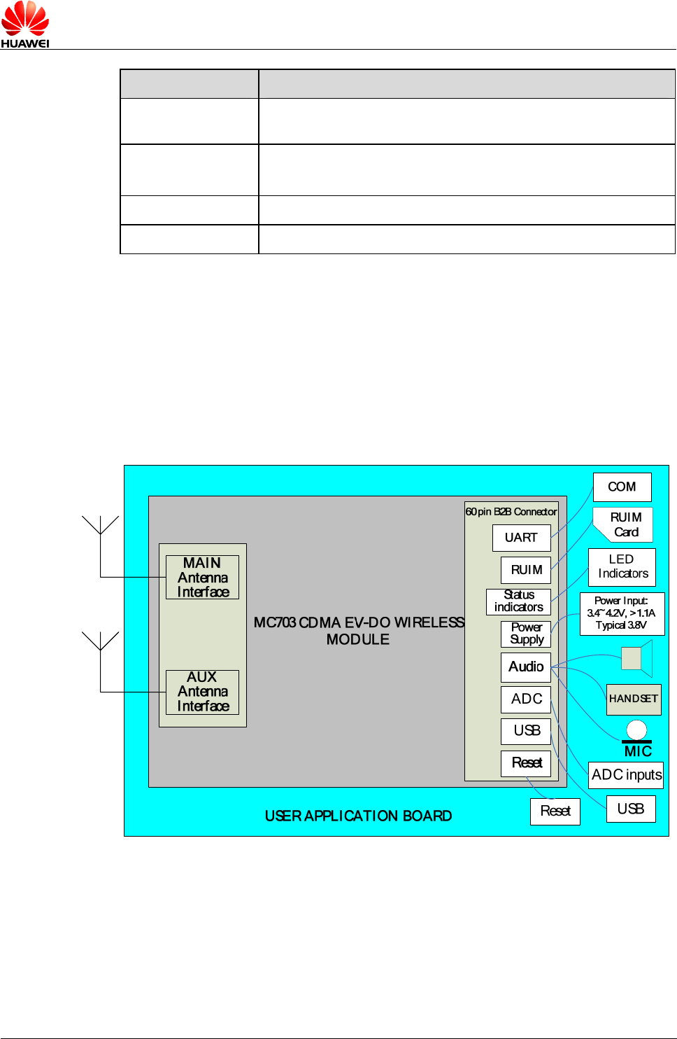
1.3 Application Block Diagram of the MC703 CDMA
EV-DO Module
O module. Figure 1-1 shows the application block diagram of the MC703 CDMA EV-D
Figure 1-1 Application block diagram of the MC703 CDMA EV-DO module
MC703 CDMA EV-DO Wireless Module
Product Description
Issue 1.00 (2009-08-24) Huawei Proprietary and Confidential Page 12 of 45
2 Interface Description
2.1 About This Chapter
gnal interfaces of the MC703 CDMA EV-DO module, with the
following interfaces included:
z Signal Connector Interface
2.2 Signal Connector Interface
2.2.1 Interface Sign
le adopts the 60-pin B2B connector as the external signal
interface.
l connector interface of the
M 3 mo .
Table 2- ns of the signals o tor interface
This chapter describes the si
z Antenna Interfaces
als
The MC703 CDMA EV-DO modu
Table 2-1 shows the function definition of the signals on the signa
C70 CDMA EV-DO dule
1 Functio n the signal connec
No. Signal Name IO Function Remarks
1 VBAT pply input he voltage ranges from 3.4
P Power su T
V to 4.2 V. The voltage of 3.8
V is recommended.
2 GND P Ground
3 VBAT pply input he voltage ranges from 3.4
P Power su T
V to 4.2 V. The voltage of 3.8
V is recommended.
4 GND P Ground
5 VBAT pply input he voltage ranges from 3.4
P Power su T
V to 4.2 V. The voltage of 3.8
V is recommended.
MC703 CDMA EV-DO Wireless Module
Product Description
Issue 1.00 (2009-08-24) Huawei Proprietary and Confidential Page 13 of 45
No. Signal Name IO Function Remarks
6 GND P Ground
7 VBAT P Power supply input The voltage ranges from 3.4
V to 4.2 V. The voltage of 3.8
V is recommended.
8 GND P Ground
9 VBAT P Power supply input The voltage ranges from 3
V to 4.2
.4
V. The voltage of 3.8
V is recommended.
10 GND P Ground
11 MODE_LED AO Mode indicator This pin is a current sink
output.
12 VCOIN P Input of the backup power supply This pin can be connected to a
e capacitance.
button-type battery or a
capacitor of larg
13 STATUS_LED AO Status indicator current sink This pin is a
output.
14 VREG_MSMP P Output of the 2.6 V voltage es voltage for
See Note 1.
This pin provid
peripherals.
15 NC - - be left
unconnected.
This pin must
16 RESET_N DI Reset Active low.
17 NC - - be left
unconnected.
This pin must
18 TERM_ON DI Active low. Power-on
19 NC - - This pin must be left
unconnected.
20 UART1_RTS DO Request To Send (RTS) signal of
UART1
21 FORCE_LOAD_N ctive low. DI Force-load signal A
22 UART1_RING DO Ringing signal of UART1
23 UART1_RD DI RD signal of UART1
24 UART1_DSR DO eady (DSR) signal of
UART1
Data set r
25 GPIO_7 IO GPIO 7
26 UART1_CTS DO d (CTS) signal of
UART1
Clear to Sen
MC703 CDMA EV-DO Wireless Module
Product Description
Issue 1.00 (2009-08-24) Huawei Proprietary and Confidential Page 14 of 45
No. Signal Name IO Function Remarks
27 UART1_TD DO TD signal of UART1
28 UART1_DTR DI eady (DTR) signal
UART1
Data terminal r
of
29 GPIO_8 IO GPIO 8
30 UART1_DCD DO Data carrier detect (DCD) signal
1
of UART
31 NC - - This pin must be left
unconnected.
32 GPIO_1 IO GPIO 1
33 GPIO_2 IO GPIO 2
34 MODULE_WAKE
UP
wake up the module by
the host
DI Signal to
35 GPIO_3 IO GPIO 3
36 USB_D- IO USB data signal, negative
37 GPIO_4 IO GPIO 4
38 USB_D+ IO USB data signal, positive
39 GPIO_5 IO GPIO 5
40 HOST_WAKEUP DO wake up the host by the Signal to
module
41 GPIO_6 IO GPIO 6
42 RUIM_CLK DO Clock signal of the RUIM
interface
43 I2C_SCL IO Clock signal of the I2C bus Reserved
44 VREG_RUIM P Power supply of the RUIM
interface
45 I2C_SDA IO Data signal of the I2C bus Reserved
46 RUIM_IO IO Data signal of the RUIM interface
47 EAR1_N AO output of the
first audio interface
Negative pole of the
48 RUIM_RST DO Reset signal of the RUIM
interface
49 EAR1_P AO utput of the
first audio interface
Positive pole of the o
50 RUIM_IN DI Signal for detecting the presence
of the RUIM card
MC703 CDMA EV-DO Wireless Module
Product Description
Issue 1.00 (2009-08-24) Huawei Proprietary and Confidential Page 15 of 45
No. Signal Name IO Function Remarks
51 MIC1_N AI Negative pole of the input of the
first audio interface
See section 4.4 "Audio
Interfaces."
52 GND P Ground
53 MIC1_P AI Positive pole of the input of the
first audio interface
54 SPKR_OUT_N e
second audio interface
AO Negative pole of the output of th
55 GND P Ground
56 SPKR_OUT_P AO Positive pole of the output of the
second audio interface
57 ADC_1 AI Input of the first ADC channel The input voltage ranges from
V to 2.6 V.
0
58 MIC2_N AI Negative pole of the input of the
second audio interface
59 e ranges from ADC_2 AI Input of the second ADC channel The input voltag
0 V to 2.6 V.
60 AI Positive pole of the input of the
second audio interface
MIC2_P
NOTE
Note 1: pin exports the voltage of 2.6 V with the capability of 50 mA.
Note 2:
IO: Digital Input/Digital Output.
2.3 Antenn
2.3.1 Anten
The MC703 CDMA EV-DO module supports the main antenna interface and the diversity
antenna interface. Both of these two antenna interfaces include two connection types, a RF
connector and an antenna pad. Either of these two antenna connection types can be selected
for use. The selected cable and antenna must have an impedance of 50 ohm.
The VREG_MSMP
Terms description:
AI: Analog Input.
AO: Analog Output.
P: Power/Ground.
DI: Digital Input.
DO: Digital Output.
NC: Not Connected.
a Interfaces
na Interface Circuits
MC703 CDMA EV-DO Wireless Module
Product Description
Issue 1.00 (2009-08-24) Huawei Proprietary and Confidential Page 16 of 45
The MC703 CDMA EV-DO module adopts the 51-3612-50-H RF connector supplied by
Astron. Figure 2-1 shows the dimensions of the RF connector.
Figure 2-1 Dimensions of the RF connector
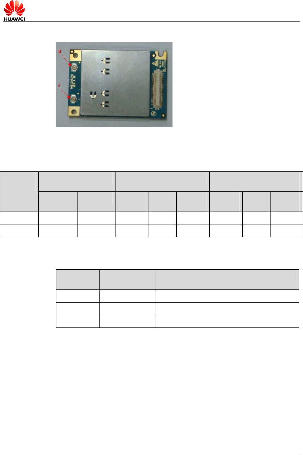
Figure 2-2 shows the RF connector. The two interfaces on the RF connector are pointed by the
red arrows. The antenna pad is located at the bottom of the RF connector. A coaxial cable
be soldere can
d on the antenna pad for connecting an external antenna to the MC703 CDMA
The RF connector and antenna pad can only be applied alternatively. When using the antenna
pad, make sure that the surface of the soldering points is smooth to reduce the impact of the
soldering on RF signals.
EV-DO module. The interface marked with M is the main diversity antenna interface and the
interface marked with A is the interface used by both the diversity antenna and the GPS
antenna.
MC703 CDMA EV-DO Wireless Module
Product Description
Issue 1.00 (2009-08-24) Huawei Proprietary and Confidential Page 17 of 45
Figure 2-2 RF connector
Table 2-2 and Table 2-3 show the RF performance of the antenna interfaces.
Table 2-2 RF performance of the main diversity antenna interface
Frequency Range (MHz) Maximum Transmit Power (dBm) Receiving Sensitivity of the
Antenna Interface (dBm)
Frequency
Band
Uplink Downlink Minimum
Value
Typical
Value
Maximum
Value
Minimum
Value
Typical
Value
Maximu
m Value
CDMA 800 824 to 849 869 to 894 23 24.5 26 / –107.5 –106
CDMA 1900 1850 to 1910 1930 to 1990 23 24.5 26 / –107.5 –106
Table 2-3 RF performance of the diversity antenna and GPS antenna interface
Frequency
Band
Frequency Range
(MHz)
Receiving Sensitivity of the Antenna Interface (dBm)
CDMA 800 869 to 894 < –106
CDMA 1900 1930 to 1990 < –106
GPS 1575.42 < –155.8 (50% Time)
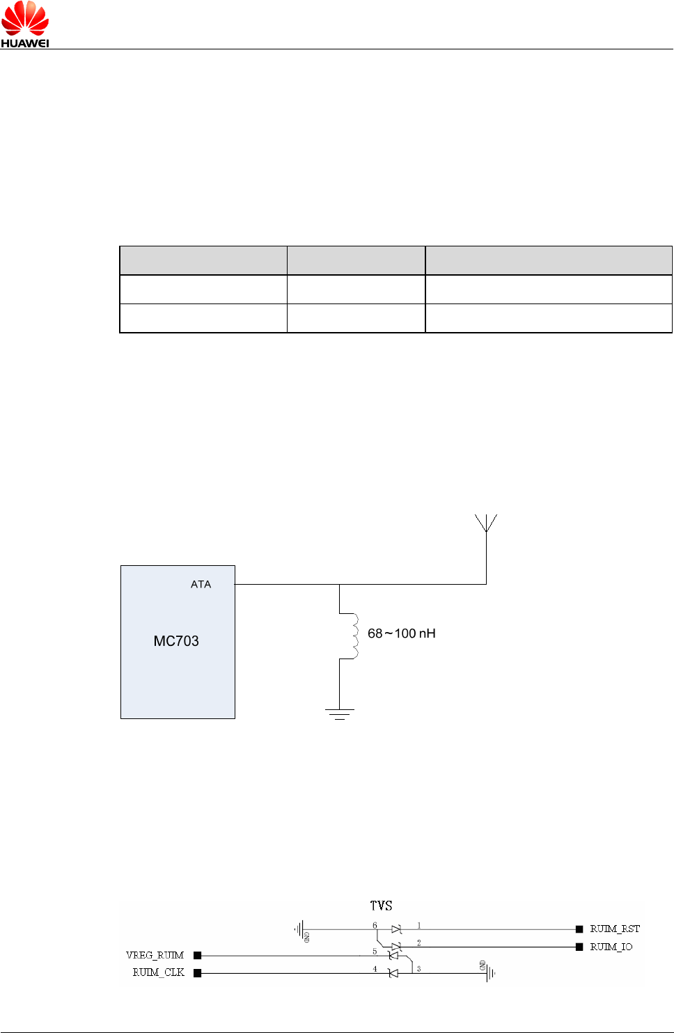
The antenna whose gain value is less than 1 dBi is recommended.
According to the layout of the circuit board, adjust the reference value of each component.
You can connect an inductor of 68 nH to 100 nH for electrostatic discharge (ESD) protection
to the ground. Pay special attention to the impedance matching of the antenna and ESD
protection capability or lightning protection capability.
MC703 CDMA EV-DO Wireless Module
Product Description
Issue 1.00 (2009-08-24) Huawei Proprietary and Confidential Page 18 of 45
3 Electrical Features of the Interfaces
3.1 About This Chapter
es of the interfaces of the MC703 CDMA EV-DO
d es included:
e Temperature
O Interface
ly Features
z
z
This chapter describes the electrical featur
mo ule with the following featur
z Application Extremes
z Operating and Storag
z Levels of the I/
z Power Supp
Reliability Features
ESD Features
the electrical features of the external interfaces of the MC703 CDMA
3.2 Applic
module. When
e may be caused to
t D odule.
T Extre e 3 CDMA EV- odule
This chapter describes mainly
EV-DO module.
ation Extremes
Table 3-1 shows the extreme application values of the MC703 CDMA EV-DO
a voltage lower or higher than the limit values is used, a permanent damag
he MC703 C MA EV-DO m
able 3-1 me application values of th MC70 DO m
Parameter Description Minimum Value Maximum Value Unit
VBAT age of the MC703
CDMA EV-DO module
–0.5 5.0 V
Input volt
VIN Input voltage of the I/O
interface
–0.5 5.0 V
MC703 CDMA EV-DO Wireless Module
Product Description
Issue 1.00 (2009-08-24) Huawei Proprietary and Confidential Page 19 of 45
3.3 Operat
Ta ws the temperature ranges of
Tf the MC703 CDMA EV-DO mo
ing and Storage Temperature
ble 3-2 sho the MC703 CDMA EV-DO module.
able 3-2 Temperature ranges o dule
Parameter Minimum Value Maximum Value Unit
Normal operating temperature –30 75 ℃
Extended operating temperature –35 80 ℃
Storage temperature –40 90 ℃
3.4 Levels
Ta nterfaces CDM
Table 3-3 Leve on the M DMA EV-DO (V PX = V)
of the I/O Interface
ble 3-3 shows the levels of the I/O i on the MC703 A EV-DO module.
ls of the I/O interfaces C703 C module DD_ 2.6
Parameter Description M um Valueinim Maximum Value Unit
VIH High-level input voltage 0.65 x VDD_PX X + 0.3 VDD_P V
VIL Low-level input voltage –0.3 5 x VDD_PX
0.3 V
VOH t voltage VDD_PX – 0.45 VDD_PX V High-level outpu
VOL e 45 Low-level output voltag 0 0. V
IIH Current leakage during
high-level input
- 1 µA
IIL Current leakage during
low-level input
–1 - µA
CIN Input capacitance - 7 pF
3.5 Power
3.5.1 Input P
Ta ws the ply ra 703 CD e.
le 3-4 Input power supply range of the MC703 CDMA EV-DO module
Supply Features
ower Supply
ble 3-4 sho input power sup nge of the MC MA EV-DO modul
Tab
Parameter Minimum Value Typical Value Maximum Value Unit
VBAT 3.4 3.8 4.2 V
MC703 CDMA EV-DO Wireless Module
Product Description
Issue 1.00 (2009-08-24) Huawei Proprietary and Confidential Page 20 of 45
The time when any interface on the MC703 CDMA EV-DO module is powered on must not
be earlier than the time when the module is pow
ered on. Otherwise, the MC703 CDMA
e abnormal or damaged.
EV-DO module may b
3.5.2 Opera
Tg curr C70 O mo
ting Current
Table 3-5 shows the operating current of the MC703 CDMA EV-DO module.
able 3-5 Operatin ent of the M 3 CDMA EV-D dule (TBD)
Operating Mode Minimum
V
Typical Value Maximum Value Unit
alue
Idle state - - TBD mA
Calling state - TBD - mA
EV-DO data
transmission state
- TBD - mA
Off state - TBD TBD µA
MC703 CDMA EV-DO Wireless Module
Product Description
Issue 1.00 (2009-08-24) Huawei Proprietary and Confidential Page 21 of 45
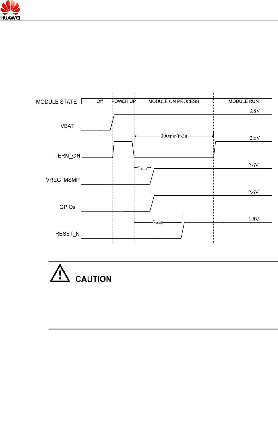
3.5.3 Power-on, Power-off, and Reset Processes
When the voltage of the power supplied to the MC703 CDMA EV-DO module is higher than
3.4 V and the TERM_ON pin is driven low for at least 300 ms, the MC703 CDMA EV-DO
module can be powered on. Figure 3-1 shows the power-on process of the MC703 CDMA
EV-DO module.
Figure 3-1 Power-on process of the MC703 CDMA EV-DO module
If the power supply with the lower voltage (for example 3.4 V) is used, the cable connecting
the external power supply and the module should be as short as possible and the power supply
input should be configured with a capacitor of higher than 1000 µF. Otherwise, the voltage
that is actually imported to the MC703 CDMA EV-DO module may be lower than 3.4 V,
resulting in the deterioration of RF indicators and unstable operation of the MC703 CDMA
EV-DO module.
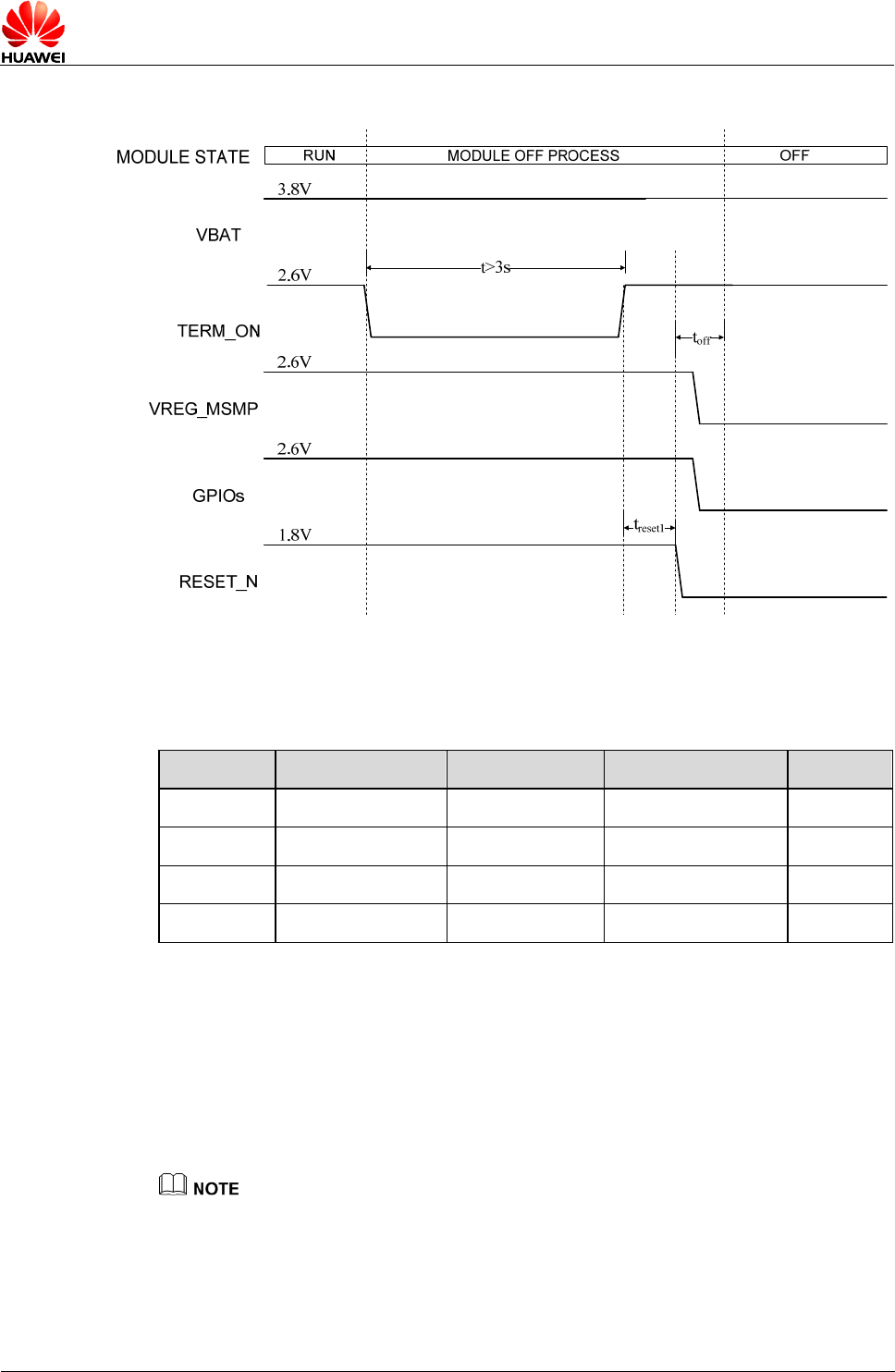
The power-off process is classified into normal power-off and urgent power-off.
Normal power-off
An external CPU drives the TERM_ON pin low for more than 3s. Then, the MC703 CDMA
EV-DO module is normally powered off. During the normal power-off process, the MC703
CDMA EV-DO module can save information and log out of the network.
Figure 3-2 shows the normal power-off process.
MC703 CDMA EV-DO Wireless Module
Product Description
Issue 1.00 (2009-08-24) Huawei Proprietary and Confidential Page 22 of 45
Figure 3-2 Normal power-off process of the MC703 CDMA EV-DO module
Table 3-6 shows the parameters in the power-on process and power-off process.
Table 3-6 Parameters in the power-on process and power-off process
Parameter Minimum Value Typical Value Maximum Value Unit
tsettle 0.36 6.36 10.36 ms
treset0 10.72 26.72 40.72 ms
treset1 400 500 600 ms
toff 7.27 10.6 15.6 ms
Urgent power-off
An external CPU sends the AT%MSO command to the MC703 CDMA EV-DO module to
directly cut off the power supply to the VBAT pin. Then, the MC703 CDMA EV-DO module
can be directly powered off.
During the urgent power-off process, the MC703 CDMA EV-DO module cannot perform the
operation of logging out of the network.
For the details about the AT%MSO command, refer to the HUAWEI MC703 Wireless Module AT
Command Interface Specification.
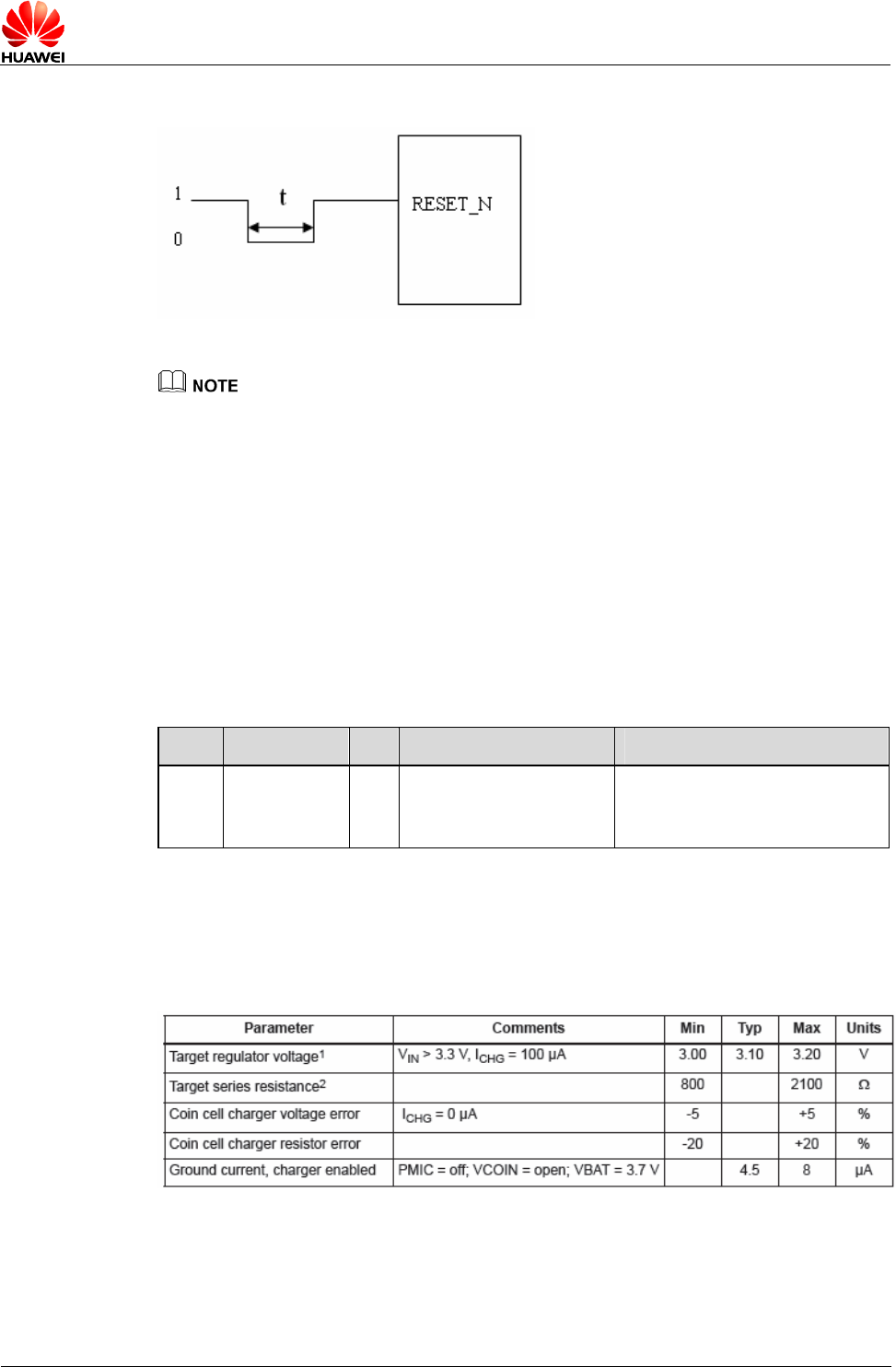
When the RESET_N pin is driven low for 50 ms, the MC703 CDMA EV-DO module can be
reset. Figure 3-3 shows the reset process of the MC703 CDMA EV-DO module.
MC703 CDMA EV-DO Wireless Module
Product Description
Issue 1.00 (2009-08-24) Huawei Proprietary and Confidential Page 23 of 45
Figure 3-3 Reset process of the MC703 CDMA EV-DO module
The RESET_N pin is sensitive to interference. Therefore, the lines on the interface board of the MC703
CDMA EV-DO module should be not longer than 2 cm. Otherwise, the MC703 CDMA EV-DO module
may be reset because of interference.
3.5.4 RTC Power Supply
The power supply pin for the real-time clock (RTC) can obtain current from the VBAT pin
through software enabling to charge the backup battery of the RTC. The power supply input is
monitored by a CPU.
The MC703 CDMA EV-DO module defines the VCOIN pin for the input of the backup power
supply on the 60-pin B2B connector to implement the power supply input for the RTC.
Table 3-7 VCOIN pin for the input of the RTC power supply
PIN Name I/O
Function Remarks
12 VCOIN P Input of the backup power
supply
This pin is connected to a button-type
battery or a capacitor of large
capacitance.
If the RTC backup battery is not used, you can connect the pin to the primary power supply,
or use an electrolytic capacitor of large capacitance.
Table 3-8 Parameters of the RTC power supply pin
MC703 CDMA EV-DO Wireless Module
Product Description
Issue 1.00 (2009-08-24) Huawei Proprietary and Confidential Page 24 of 45
3.6 Reliability Features
Table 3-9 shows the conditions and results of the part mechanical reliability tests performed
on the MC703 CDMA EV-DO module.
Table 3-9 Conditions and results of the part mechanical reliability tests
Test Item Test Condition Test Standard
Random vibration Frequency range: 5 Hz to 20 Hz, PSD: 1.0 m²/s3;
Frequency range: 20 Hz to 200 Hz, –3 dB/oct;
Three axial directions with one hour for each
direction
IEC 68-2-6
Shock test Half sine wave shock
Acceleration: 20 g
Shock period: 11 ms
Six axial directions with one shock in each direction
(± x, y, and z)
TIA/EIA 603 3.3.5
GB/T15844.2 4.1
Temperature shock Low temperature: –40°C±2°C
High temperature: 85°C±2°C
Changeover time: < 30s
Test duration: 1 hour
Repetition times: 100
IEC 68-2-14 Na
Damp heat cyclic High temperature: 55°C±2°C
Low temperature: 25°C±2°C
Humidity: 95%
Repetition times: 4
Test duration: 12 hours + 12 hours
IEC 68-2-30 Db
Low-temperature
operation
Temperature: –30°C±2°C
Test period: 24 hours
IEC 68-2-1 Ab
High-temperature
operation
Temperature: 75°C±2°C
Test period: 24 hours
IEC 68-2-2 Bb
Low-temperature
storage
Temperature: –60°C±2°C
Test period: 24 hours
IEC 68-2-1 Ab
High-temperature
storage
Temperature: 90°C±2°C
Test period: 24 hours
IEC 68-2-2 Bb
Salt spray test Temperature: 35°C
Density of the NaCl solution: 5%±1%
Spraying duration: 48 hours
Duration of exposing the module to the temperature
of 35 ºC: 16 hours
IEC 68-2-11
MC703 CDMA EV-DO Wireless Module
Product Description
Issue 1.00 (2009-08-24) Huawei Proprietary and Confidential Page 25 of 45
3.7 ESD Features
3.7.1 Overview
When the MC703 CDMA EV-DO module is in use, the ESD protection should be considered.
The ESD performance of the MC703 CDMA EV-DO module has been tested according to the
EN61000-4-2 standard. Table 3-10 shows the test results.
Table 3-10 ESD performance
Interface Air Discharge Contact Discharge
RUIM card interface ±8000 V ±4000 V
USB interface ±8000 V ±4000 V
3.7.2 ESD Protection on the Antenna Interface
The antenna interface of the MC703 CDMA EV-DO module is sensitive to ESD. Poor ESD
protection may cause permanent damage to internal RF components. Figure 3-4 shows the
recommended circuit for the ESD protection on the antenna interface.
Figure 3-4 Recommended circuit for the ESD protection on the antenna interface
3.7.3 ESD Protection on the RUIM Card Interface
Figure 3-5 shows the recommended circuit for the ESD protection on the RUIM card interface
of the MC703 CDMA EV-DO module. The transient voltage suppressor (TVS) diode should
be placed as close to the RUIM card seat as possible.
Figure 3-5 Recommended circuit for ESD protection on the RUIM card interface

MC703 CDMA EV-DO Wireless Module
Product Description
Issue 1.00 (2009-08-24) Huawei Proprietary and Confidential Page 26 of 45

MC703 CDMA EV-DO Wireless Module
Product Description
Issue 1.00 (2009-08-24) Huawei Proprietary and Confidential Page 27 of 45
4 Interface Applications
4.1 About This Chapter
pplications of the interfaces of the MC703 CDMA EV-DO module,
th rfaces included:
d Interface
terface
z ADC Interfaces
z Status Indication Pins
4.2 UART Interface
a
rol function and a maximum transmission rate
UART1 supports programmable data width, data stop bit, and parity check (or no parity
check). In addition, UART1 supports a maximum baud rate of 230.4 kbps and a default baud
rate of 115.2 kbps. The set baud rate can be saved even if the interface is powered off.
This chapter describes the a
wi the following inte
z UART Interface
z RUIM Car
z Audio Interfaces
z Power Supply In
z USB Bus
z GPIO Interface
z Pin Sequence
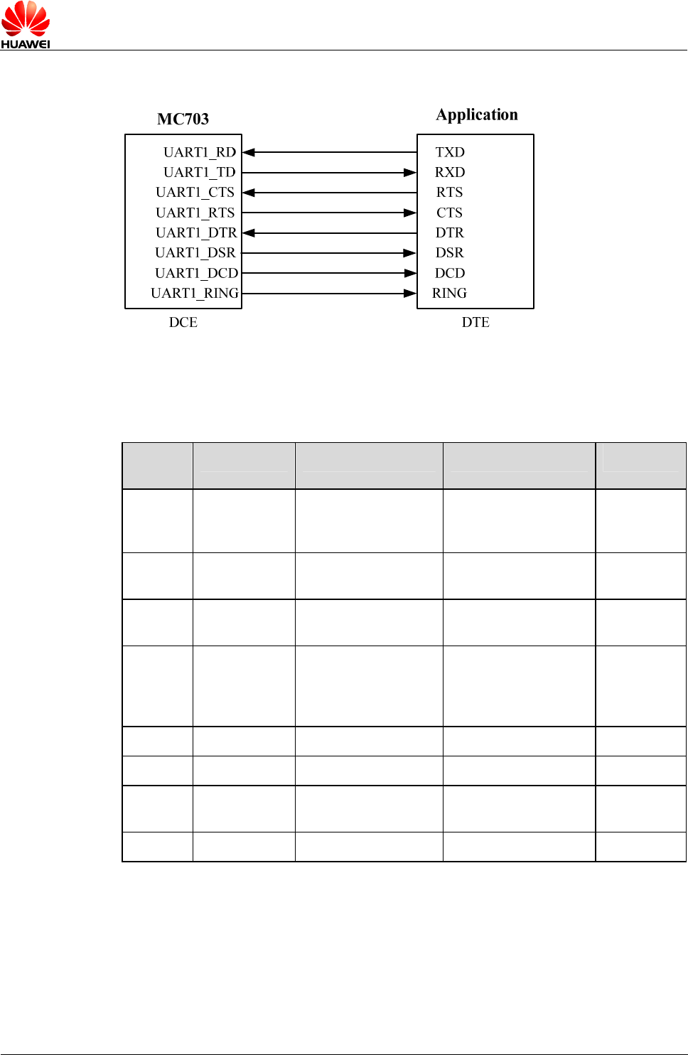
The MC703 CDMA EV-DO module has one UART interface, that is, UART1. UART1 is
9-wire serial interface supporting the flow cont
of 4 Mbit/s.
UART1 supports data services. You can set up the Point-to-Point Protocol (PPP) dial-up
connection for data services through UART1.
MC703 CDMA EV-DO Wireless Module
Product Description
Issue 1.00 (2009-08-24) Huawei Proprietary and Confidential Page 28 of 45
Figure 4-1 Connections between the DCE and DTE
Table 4-1 shows the definitions of the interface signals.
Table 4-1 Signals on UART1 of the MC703 CDMA EV-DO module
Pin
Number
Signal Name Description Feature Direction
27 UART1_TD Data transmission end of
the module
The Date Terminal
Equipment (DTE)
receives serial data.
DCE–DTE
23 UART1_RD Data receiving end of the
module
The DTE transmits serial
data.
DTE–DCE
22 UART1_RING Ringing indication of the
module
The DTE is notified of a
remote call.
DCE–DTE
20 UART1_RTS RTS on the module The DTE notifies the Data
Communications
Equipment (DCE) of
sending requests.
DCE–DTE
28 UART1_DTR DTR on the module The DTE is ready. DTE–DCE
24 UART1_DSR DSR on the module The DCE is ready. DCE–DTE
26 UART1_CTS CTS on the module The DCE switches to the
receiving mode.
DTE–DCE
30 UART1_DCD DCD on the module Data links are connected. DCE–DTE
MC703 CDMA EV-DO Wireless Module
Product Description
Issue 1.00 (2009-08-24) Huawei Proprietary and Confidential Page 29 of 45
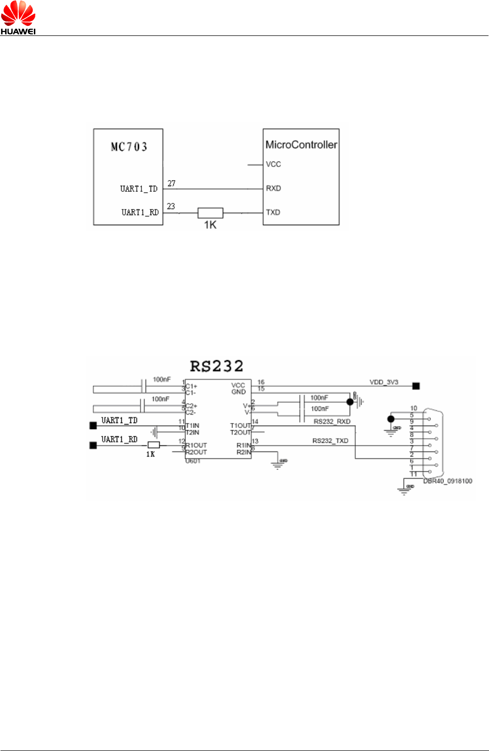
When MC703 CDMA EV-DO module is connected to a 3V single-chip microcontroller. a
1000-ohm resistor should be added between the pin UART1_RD and the pin TXD of the
microcontroller.
Figure 4-2 Connections between the serial interface and the 3 V single-chip microcontroller
You can use a Category 232 chip to connect the MC703 CDMA EV-DO module to a standard
RS-232-C interface. In the case of a 3-wire serial interface, the MAX3232 chip is
recommended. The UART1-RD pin of the module connects to the TXD pin of the DTE after
being converted through the MAX3232 chip, and the TXD pin of the DTE connects to the
UART1_TD pin of the module after being converted through the MAX232 chip.
Figure 4-3 Connections for the 3-wire serial interface
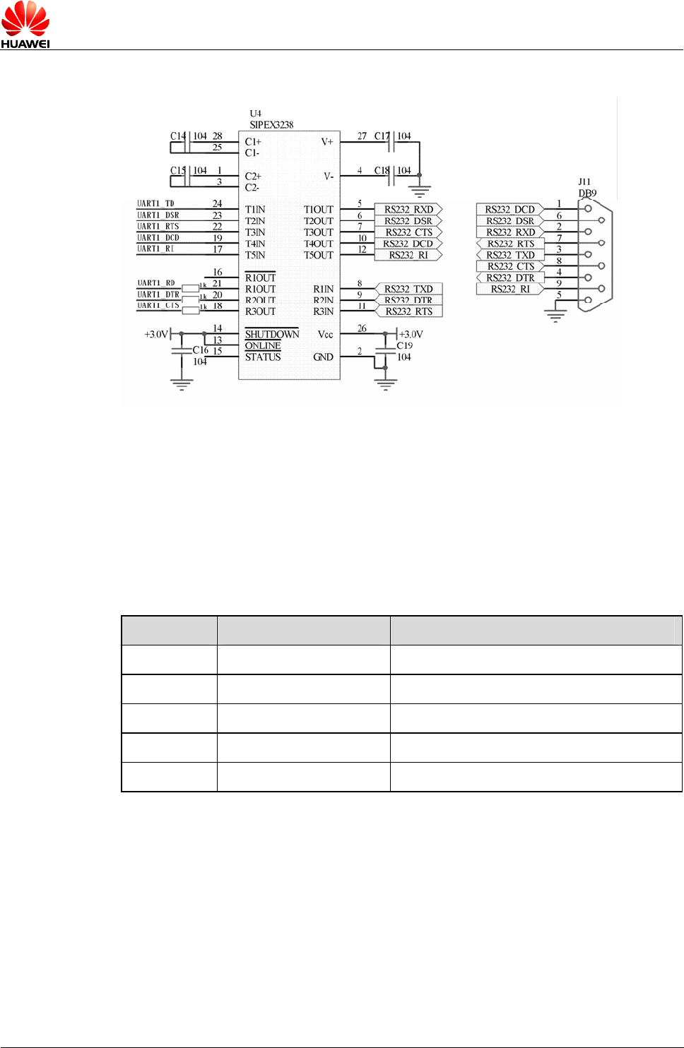
In the case of a full-serial interface, the MAX3232, SP3238, or MAX3238 chip is
recommended.
MC703 CDMA EV-DO Wireless Module
Product Description
Issue 1.00 (2009-08-24) Huawei Proprietary and Confidential Page 30 of 45
Figure 4-4 Electrical connections for the 9-wire serial interface with the flow control function
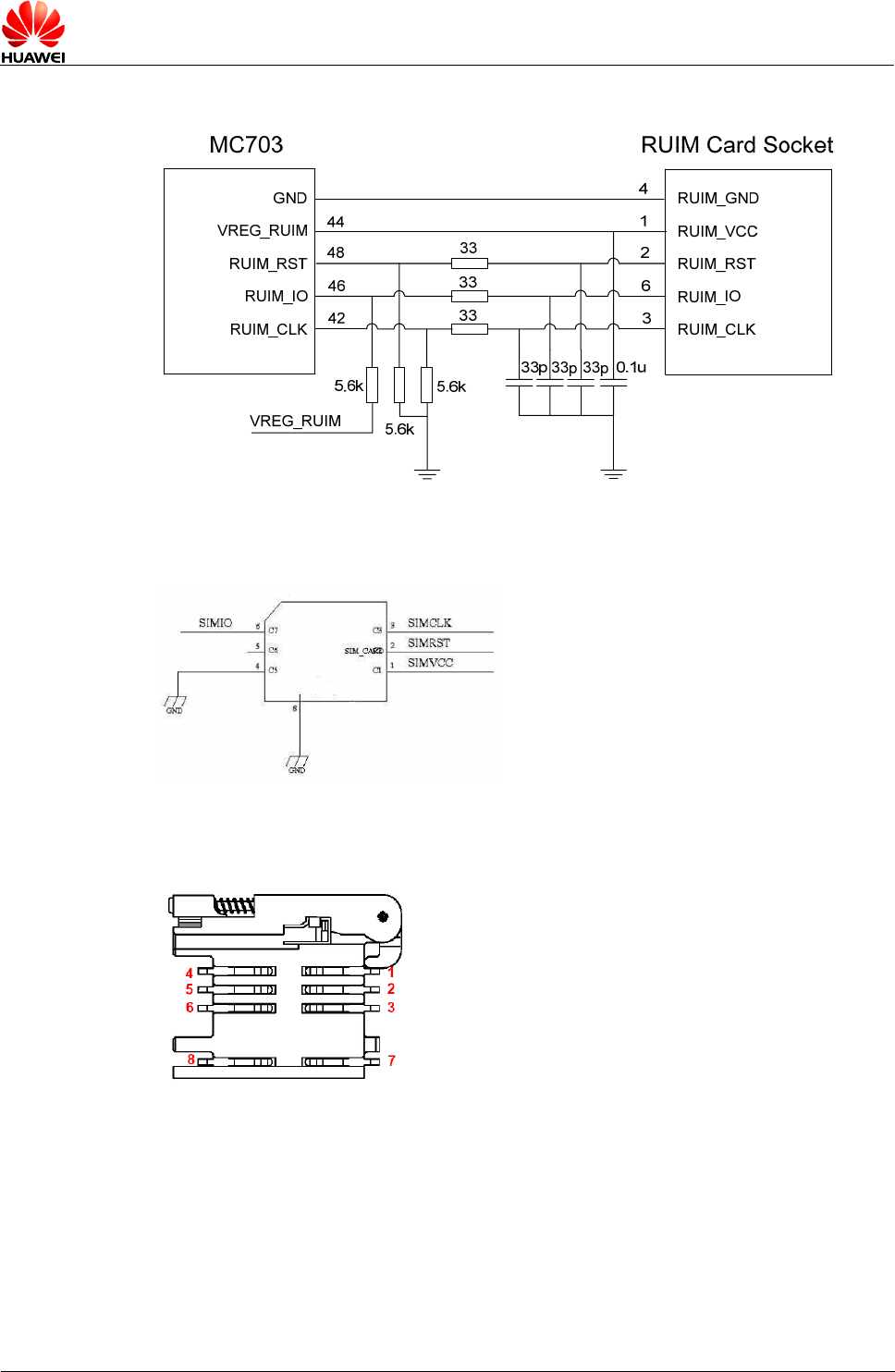
4.3 RUIM Card Interface
The MC703 CDMA EV-DO module can connect to a 3 V or a 1.8 V RUIM card. Table 4-2
shows the signals of the RUIM card interface. The level of the RUIM card interface is 3 V or
1.8 V.
Table 4-2 Pins of the RUIM card interface
Pin Number Signal Name Description
44 VREG_RUIM Power supply of the RUIM card
48 RUIM_RST Reset signal of the RUIM card
42 RUIM_CLK Clock signal of the RUIM card
46 RUIM_IO Data signal of the RUIM card
GND Ground
MC703 CDMA EV-DO Wireless Module
Product Description
Issue 1.00 (2009-08-24) Huawei Proprietary and Confidential Page 31 of 45
Figure 4-5 Circuits of the RUIM card interface
Figure 4-6 Sequence of the pins of the RUIM card
Figure 4-7 Sequence of the pins of a RUIM card socket
The typical rate of the RUIM card interface is about 3.25 MHz. Therefore, the RUIM card
seat should be as close to the module interface as possible and the line should not exceed 10
cm. This prevents the communications quality of signals from being affected by serious
waveform distortion because of too long lines. Ground lines should be used to enclose the
lines used for transmitting RUIM_CLK signals and RUIM_IO signals.
To filter out the interference from antenna signals, you need to add a 0.1µF or a 0.22µF
capacitor to the RUIM_VCC signal and a 33pF capacitor to the RUIM_CLK, RUIM_IO, and
RUIM_RST signals based on the GND network. In addition, you need to add TVS diodes to
MC703 CDMA EV-DO Wireless Module
Product Description
Issue 1.00 (2009-08-24) Huawei Proprietary and Confidential Page 32 of 45
these four signals for ESD protection. The TVS diodes should be placed as close to the RUIM
card socket as possible.
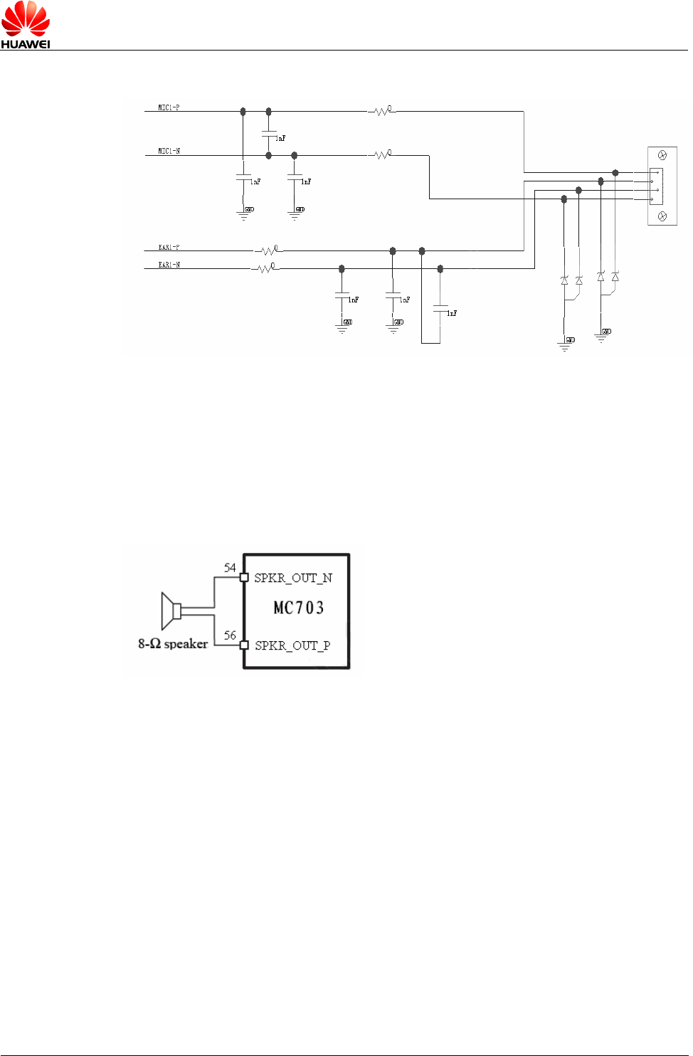
4.4 Audio Interfaces
The MC703 CDMA EV-DO module provides two audio channels and each channel includes
one input and one output interfaces. Table 4-3 shows the signals of the audio interfaces.
Table 4-3 Signals of the audio interfaces
Pin Number Signal Name Description
51 MIC1_N Negative pole of the input of the first audio interface
53 MIC1_P Positive pole of the input of the first audio interface
47 EAR1_N Negative pole of the output of the first audio interface
49 EAR1_P Positive pole of the output of the first audio interface
58 MIC2_N Negative pole of the input of the second audio interface
60 MIC2_P Positive pole of the output of the second audio interface
54 SPKR_OUT_N Negative pole of the output of the second audio interface
56 SPKR_OUT_P Positive pole of the output of the second audio interface
The input and output signals on the first audio interface are fully differential and thus have
good performance of resisting RF interference. This audio interface can be used in handset
connection mode without any external audio frequency amplifier (AFA).
As the audio signals are in differential pairs, the lines on the printed circuit board (PCB)
should be equidistantly laid in parallel with each other. The lines should be as short as
possible, the filter circuits of the two sides should be symmetric, the differential pair signals
should be close to each other, and the grounding is required. The differential pair signals of
the audio output and the differential pair signals of the audio output should be effectively
separated through grounding. In addition, the signals should be away from the circuits of the
power supply, RF, and antenna.
Differentiate and isolate functional modules during PCB design of the application board
which the MC703 CDMA EV-DO module is applied on.
MC703 CDMA EV-DO Wireless Module
Product Description
Issue 1.00 (2009-08-24) Huawei Proprietary and Confidential Page 33 of 45
Figure 4-8 Circuits of the first audio interface
Differential signals are transmitted on the first audio interface. By reserving a place for the
resistor in the loop, you can adjust the quality and volume of the voice. It is recommended
that you place a TVS on the related interface to provide protection against ESD and protect
components such as the internal integrated circuit (IC) component.
The output signals of the second audio interface can directly drive an 8-ohm speaker.
Figure 4-9 Connections between the MC703 CDMA EV-DO module and the 8-ohm speaker
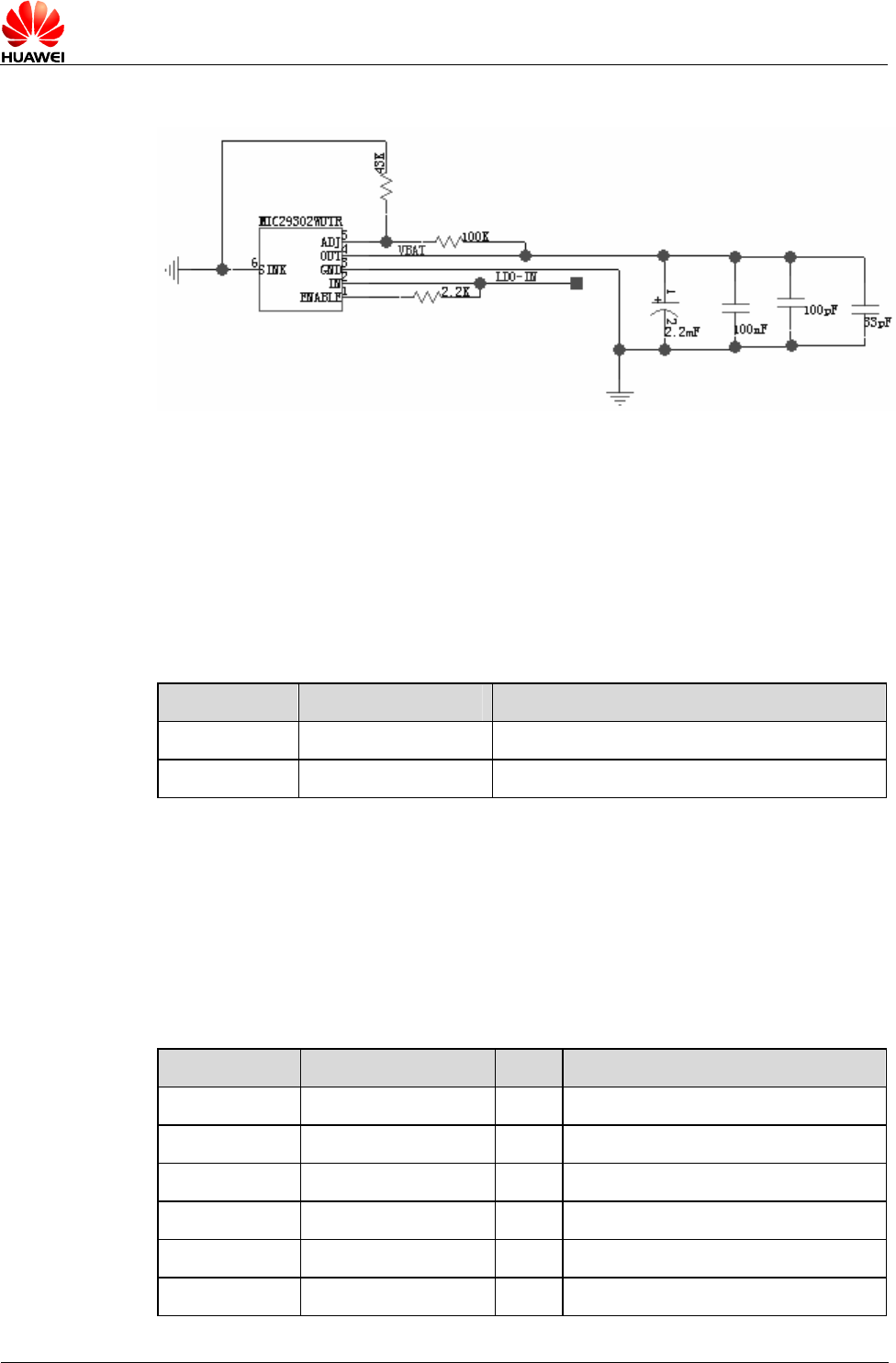
4.5 Power Supply Interface
An external power supply with the voltage of 3.3 V to 4.2 V (the typical value is 3.8 V)
powers the MC703 CDMA EV-DO module through the VBAT pin. When the network signals
are weak, the antenna transmits signals with the highest power and the maximum transient
current can be up to 1.1A. In this case, it is recommended that you use a low dropout (LDO)
regulator or a switching-mode power supply whose current is higher than 1.1 A.
Considering the voltage drop that may occur during the transmission with high power, you
can add a large capacitor on the power supply interface of the module. The electrolytic
capacitor of over 220 µF is recommended.
MC703 CDMA EV-DO Wireless Module
Product Description
Issue 1.00 (2009-08-24) Huawei Proprietary and Confidential Page 34 of 45
Figure 4-10 Reference circuits for the design of the LDO power supply
4.6 USB Bus
Working with the drives of a PC, the USB interface can be mapped to a serial interface of the
PC. The USB interface is mainly used for updating module applications, capturing software
logs, and testing module applications.
Table 4-4 Signals of the USB interface
Pin Number Signal Name Description
36 USB_D- USB data line
38 USB_D+ USB data line
4.7 GPIO Interface
The MC703 CDMA EV-DO module supports up to eight GPIO interfaces. Table 4-5 shows
the signals of the GPIO interfaces.
Table 4-5 Signals of the GPIO interfaces
Pin Number Signal I/O Description
32 GPIO_1 I/O GPIO 1
33 GPIO_2 I/O GPIO 2
35 GPIO_3 I/O GPIO 3
37 GPIO_4 I/O GPIO 4
39 GPIO_5 I/O GPIO 5
41 GPIO_6 I/O GPIO 6
MC703 CDMA EV-DO Wireless Module
Product Description
Issue 1.00 (2009-08-24) Huawei Proprietary and Confidential Page 35 of 45
Pin Number Signal I/O Description
25 GPIO_7 I/O GPIO 7
29 GPIO_8 I/O GPIO 8
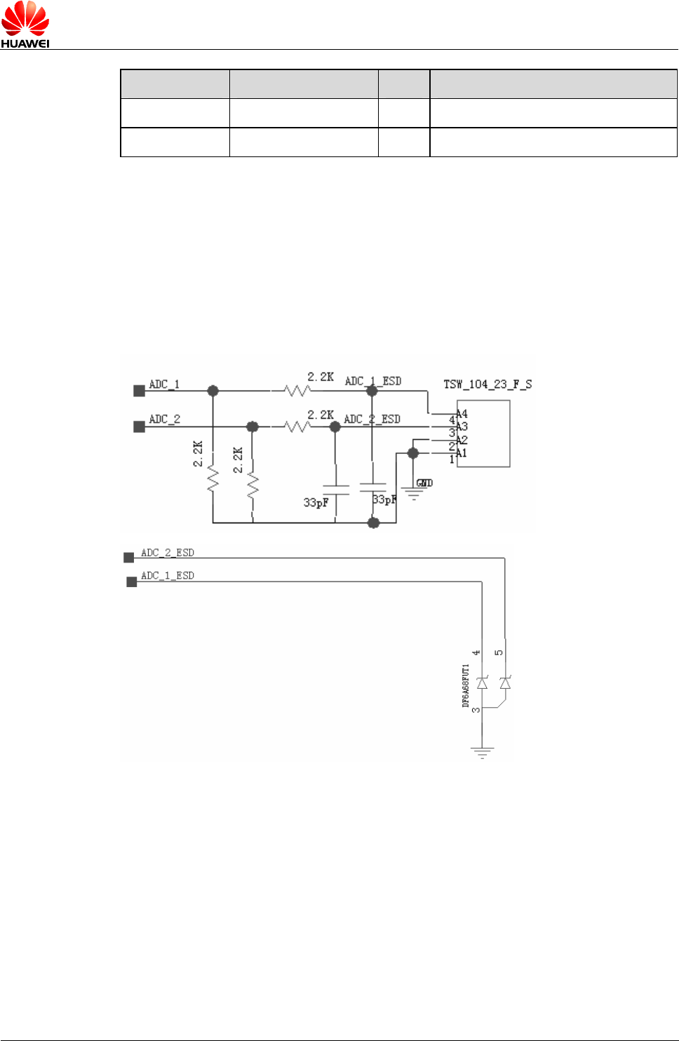
4.8 ADC Interfaces
The MC703 CDMA EV-DO module supports two ADC interfaces for monitoring analog
variables, such as the environmental temperature variable.
Figure 4-11 Reference circuits of the design of the ADC interfaces
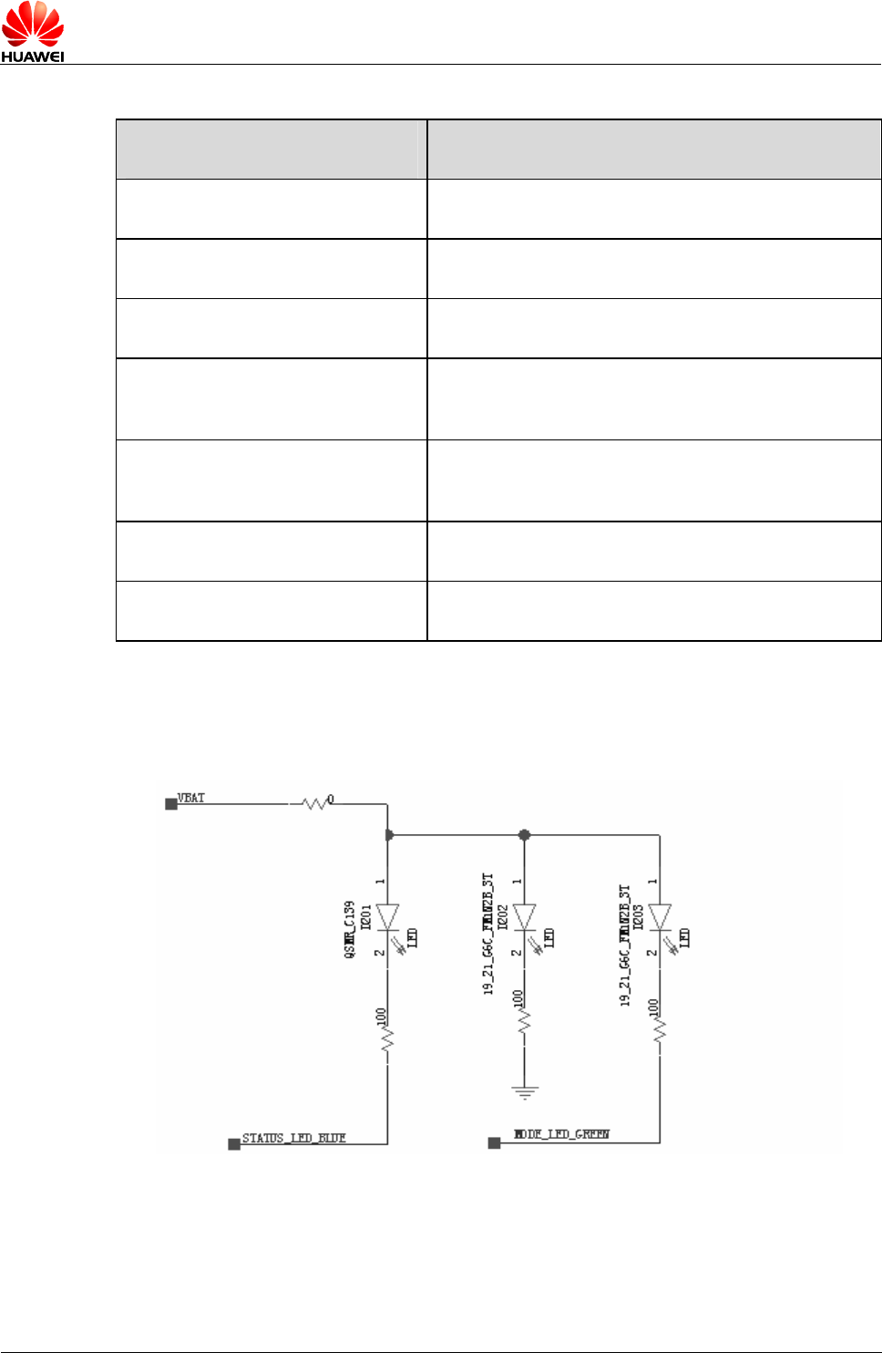
4.9 Status Indication Pins
4.9.1 LED Circuits
The MC703 CDMA EV-DO module supplies two signals which can be used to light the LEDs.
One LED indicates the network mode and the other LED indicates the signal status. The
LEDs are controlled by the current sink. The high voltage is the voltage of VBAT (with the
typical value of 3.8 V).
Table 4-6 shows the status of the LEDs.
MC703 CDMA EV-DO Wireless Module
Product Description
Issue 1.00 (2009-08-24) Huawei Proprietary and Confidential Page 36 of 45
Table 4-6 Status of the LEDs
Operating Mode of the MC703 CDMA
EV-DO Module LED Status
The module is searching for a network or no
network is available.
The LED flashes once. (The LED is on for 100 ms and off for
0.9s. Each cycle lasts 1s.)
The module finds out a 2G network. The LED flashes once. (The LED is on for 100 ms and off for
1.9s. Each cycle lasts 2s.)
The module finds out a 3G network. The LED flashes once. (The LED is on for 100 ms and off for
2.9s. Each cycle lasts 3s.)
The module is processing the CDMA 1X
data services through the dial-up service.
The LED flashes twice. (The LED is on for 100 ms and off for
300 ms, and then on for 100 ms and off for 1.5s. Each cycle lasts
2s.)
The module is processing the EV-DO data
services through the dial-up service.
The LED flashes twice. (The LED is on for 100 ms and off for
200 ms, and then on for 100 ms and off for 600 ms. Each cycle
lasts 1s.)
The module is in factory test mode (FTM). The LED flashes slowly. (The LED is on for 1s and off for 1s.
Each cycle lasts 2s.)
The module is upgrading software. The LED flashes quickly. (The LED is on for 100 ms and off for
100 ms. Each cycle lasts 0.2s.)
Figure 4-12 shows the recommended circuits of the LED pins.
Figure 4-12 Recommended circuits of the LED pins
MC703 CDMA EV-DO Wireless Module
Product Description
Issue 1.00 (2009-08-24) Huawei Proprietary and Confidential Page 37 of 45
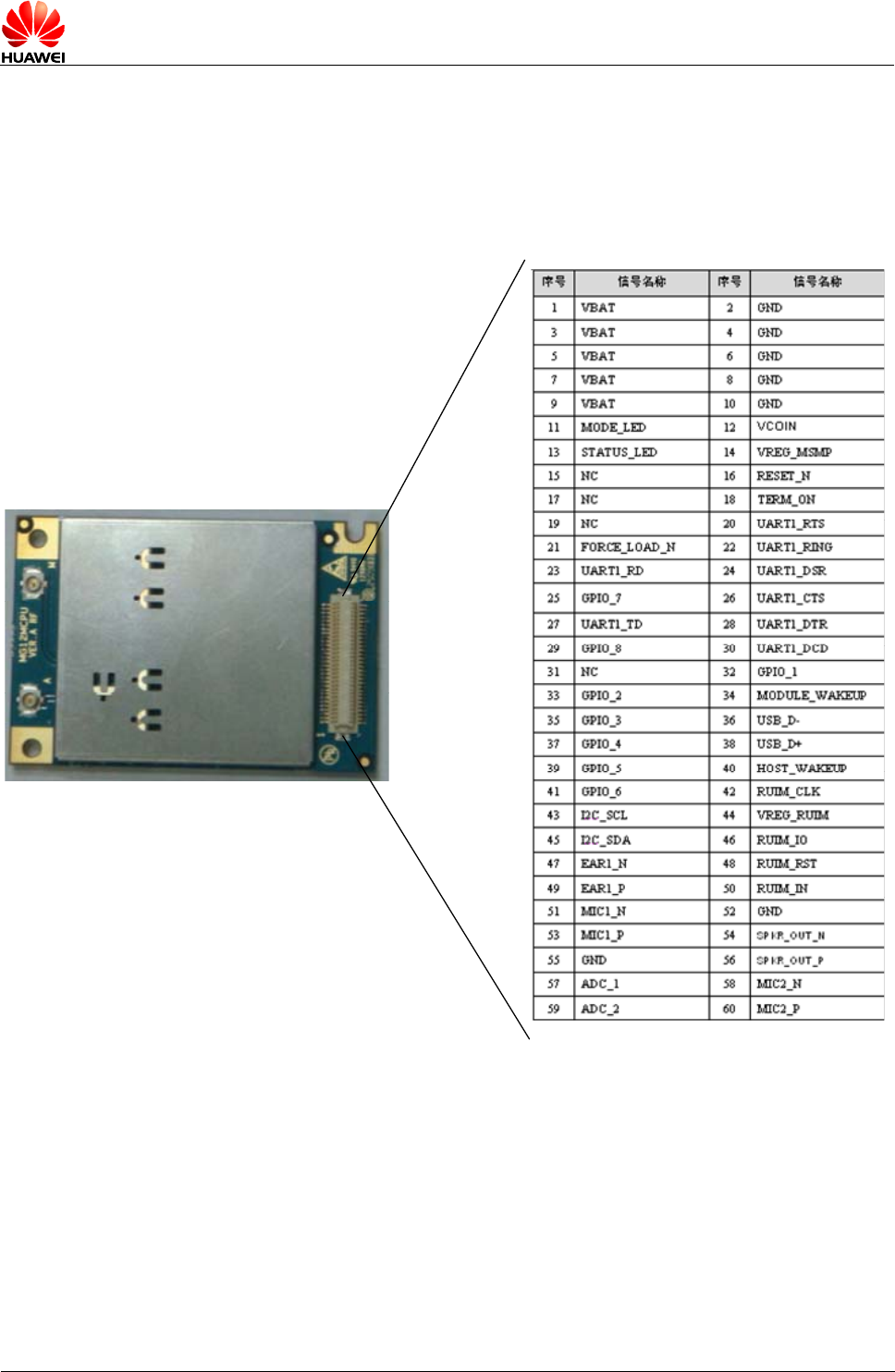
4.10 Pin Sequence
Figure 4-13 shows the sequence of the pins on the 60-pin B2B connector of the MC703
CDMA EV-DO module.
Figure 4-13 Sequence of the pins on the MC703 CDMA EV-DO module
6059
21

MC703 CDMA EV-DO Wireless Module
Product Description
Issue 1.00 (2009-08-24) Huawei Proprietary and Confidential Page 38 of 45
5 Mechanics
5.1 Overview
the MC703 CDMA EV-DO module,
with the following dimensions included:
z Mechanical Dimensions of the MC703 CDMA EV-DO Module
5.2 Mechanical Dimensions of the MC703 CDMA EV-DO
Module
Weight: 9.8 (±0.2) g
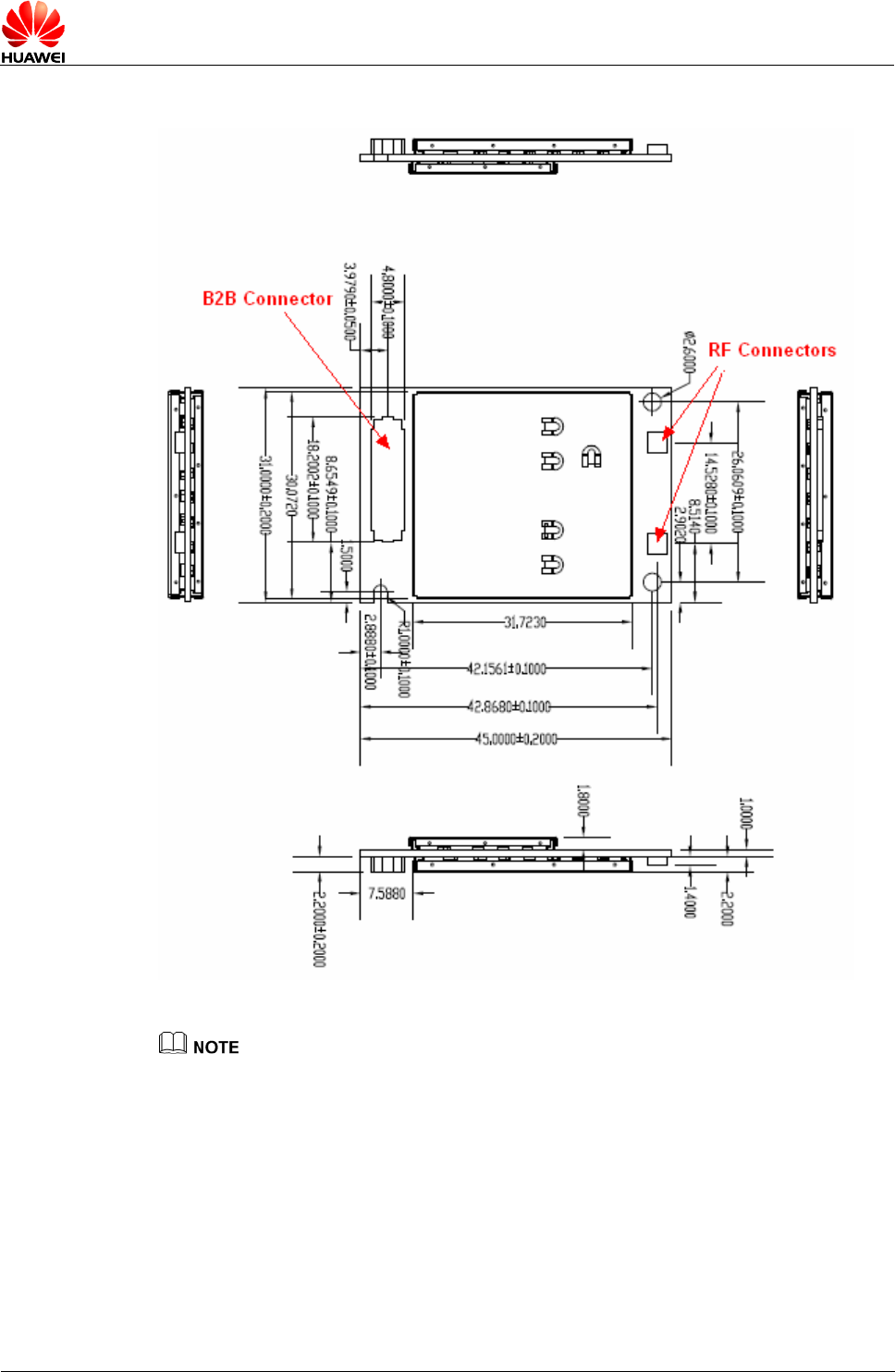
Figure 5-1 shows the mechanical dimensions of the MC703 CDMA EV-DO module.
This chapter describes the mechanical dimensions of
z Mechanical Dimensions of the B2B Connector
Dimensions: 31±0.20 mm x 45±0.20 mm x 5±0.20 mm
MC703 CDMA EV-DO Wireless Module
Product Description
Issue 1.00 (2009-08-24) Huawei Proprietary and Confidential Page 39 of 45
Figure 5-1 Mechanical dimensions of the MC703 CDMA EV-DO module (unit: mm)
If the MC703 CDMA EV-DO module is required to be compatible with other products, such as the
MU103 module, it is recommended that the mounting hole close to the B2B connector on the user
application board should be designed to be track-shaped, as shown in Figure 5-2.
MC703 CDMA EV-DO Wireless Module
Product Description
Issue 1.00 (2009-08-24) Huawei Proprietary and Confidential Page 40 of 45
Figure 5-2 Recommended shape of the toaling hole close to the B2B connector on the user
application board
Figure 5-3 Mechanical dimensions of the MU103 module
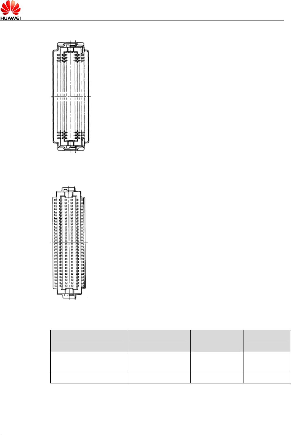
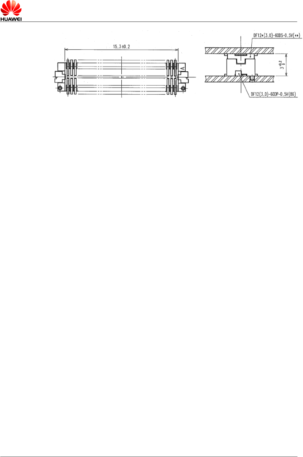
5.3 Mechanical Dimensions of the B2B Connector
The MC703 CDMA EV-DO module adopts the DF12(3.0)-60DS-0.5V(86) 60-pin B2B
connector supplied by HRS, with the pin spacing of 0.5 mm, the stacking height of 3 mm, and
pluggable times of less than 50. The connector can be mated with the
DF12(3.0)-60DP-0.5V(86), DF12(3.5)-60DP-0.5V(86), DF12(4.0)-60DP-0.5V(86), and
DF12(5.0)-60DP-0.5V(86) supplied by HRS.
MC703 CDMA EV-DO Wireless Module
Product Description
Issue 1.00 (2009-08-24) Huawei Proprietary and Confidential Page 41 of 45
Figure 5-4 HRS DF12(3.0)-60DS-0.5V(86) connector on the MC703 CDMA EV-DO module
Figure 5-5 HRS DF12(3.0)-60DP-0.5V(86) mating header on the user board
Table 5-1 DF12 series that are compatible with the MC703 CDMA EV-DO module
Product Model Stacking Height
(mm)
HRS Number
Connector used on the MC703
CDMA EV-DO module
DF12(3.0)-60DS-0.5V(86) 3.0 537-0611-1-86
Headers on the interface board DF12(3.0)-60DP-0.5V(86) 3.0 537-0731-3-86
MC703 CDMA EV-DO Wireless Module
Product Description
Issue 1.00 (2009-08-24) Huawei Proprietary and Confidential Page 42 of 45
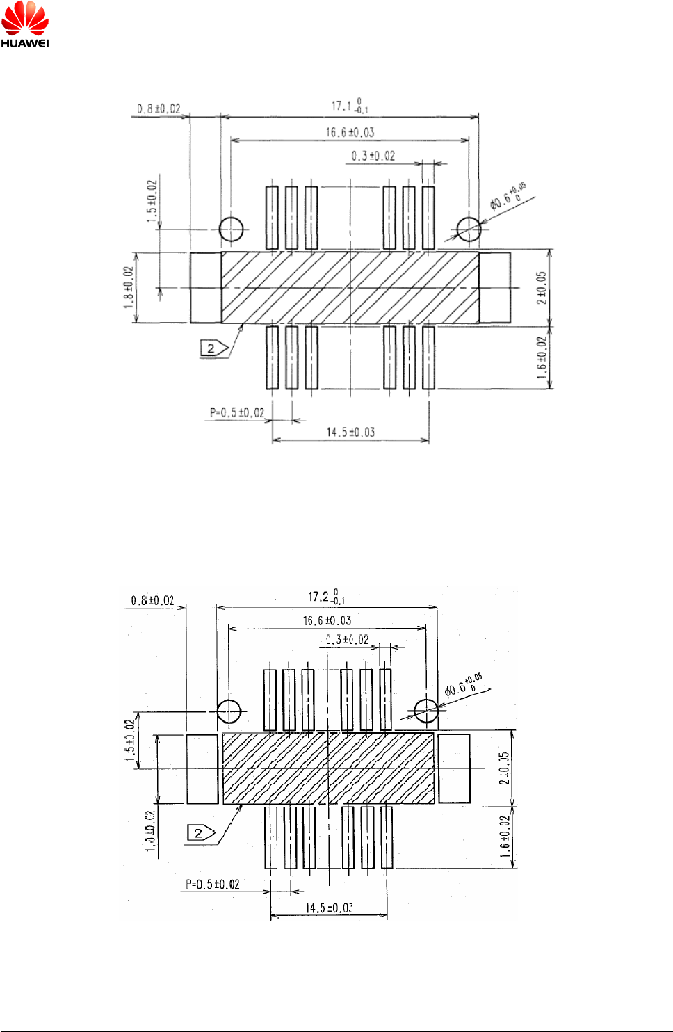
Figure 5-6 Dimensions of the connector on the MC703 CDMA EV-DO module (unit: mm)
For more information about the connectors of Hirose, access
http://www.hirose-connectors.com.
Figure 5-7 Dimensions of the connector pad on the user interface board of the MC703 CDMA
EV-DO module
MC703 CDMA EV-DO Wireless Module
Product Description
Issue 1.00 (2009-08-24) Huawei Proprietary and Confidential Page 43 of 45
MC703 CDMA EV-DO Wireless Module
Product Description
Issue 1.00 (2009-08-24) Huawei Proprietary and Confidential Page 44 of 45
A Acronyms and Abbreviations
AMR Adaptive Multi-rate
BER Bit Error Rate
BTS Base Transceiver Station
B2B Board-to-Board Connector
CSD Circuit Switched Data
DSP Digital Signal Processor
DCE Data circuit-terminating equipment
DTE Data terminal equipment
DTR Data Terminal Ready
DTX Discontinuous Transmission
EFR Enhanced Full Rate
EGSM Enhanced GSM
EMC Electromagnetic Compatibility
ESD Electrostatic Discharge
GMSK imum Shift Keying Gaussian Min
IMEI ty International Mobile Equipment Identi
I/O Input/Output
ISO International Standards Organization
ITU International Telecommunications Union
kbps kbits per second
LED Light Emitting Diode
MO Mobile Originated
MT Mobile Terminated

MC703 CDMA EV-DO Wireless Module
Product Description
Issue 1.00 (2009-08-24) Huawei Proprietary and Confidential Page 45 of 45
NTC Negative Temperature Coefficient
PCS Personal Cellular System
PCL Power Control Level
PCS Personal Communication System
PPP Point-to-point protocol
QPSK Quadrate Phase Shift Keying
RTC Real Time Clock
UART Universal asynchronous receiver-transmitter
EV-DO Evolution-Data Only
VSWR Voltage Standing Wave Ratio