Huawei Technologies ME309-562 eMTC Module User Manual pt 1
Huawei Technologies Co.,Ltd eMTC Module pt 1
UserManual.wiki
>
Huawei Technologies
>
ME309-562 User Manual
>
User Manual pt 1
Contents
1.
Users Manual 1
2.
User Manual 2
3.
User Manual pt 1
4.
User manual pt 2
User Manual pt 1
Navigation menu
Upload a User Manual
Namespaces
Wiki Guide
HTML
PDF
Info
Views
User Manual
Discussion / Help
Navigation
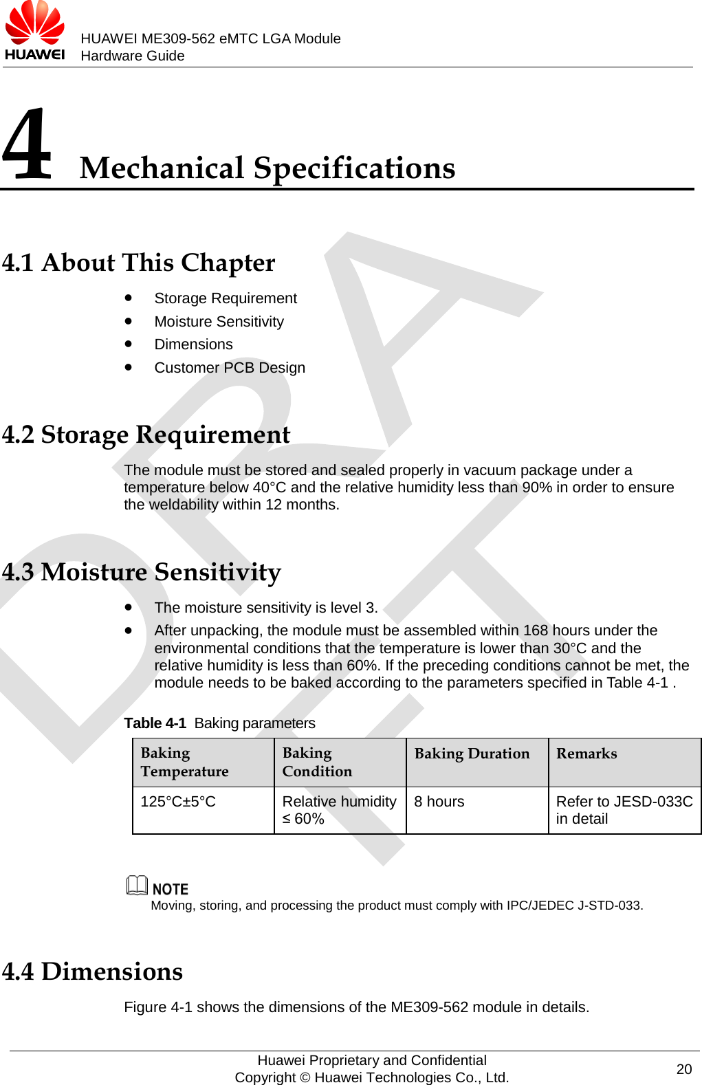
![HUAWEI ME309-562 eMTC LGA Module Hardware Guide 2 Overall Description 2.1 About This Chapter This chapter gives a general description of the ME309-562 module and provides: Function Overview Circuit Block Diagram Application Block Diagram 2.2 Function Overview Table 2-1 ME309-562 module features Feature Description Physical Dimensions Dimensions (W × L × H): 18 mm × 24 mm × 2.5 mm Weight TBD Operating Bands HD-FDD LTE: Band 2, Band 4, Band 12, Band13 Operating Temperature Normal operating temperature: –30°C to +75°C (Characteristics guaranteed) Extended operating temperature[1]: –40°C to +85°C (Normal working) Storage Temperature –40°C to +95°C Power Voltage 3.3 V to 4.2 V (3.8 V is recommended.) Huawei Proprietary and Confidential Copyright © Huawei Technologies Co., Ltd. 6](https://usermanual.wiki/Huawei-Technologies/ME309-562.User-Manual-pt-1/User-Guide-3748049-Page-6.png)
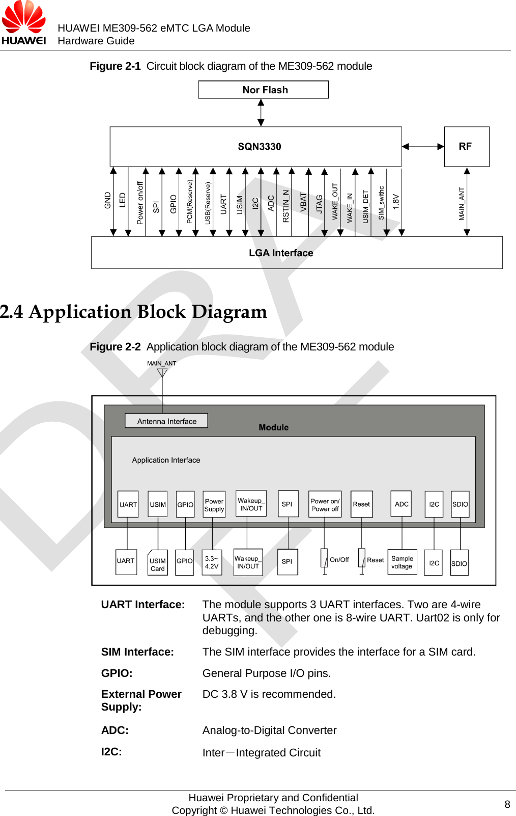
![HUAWEI ME309-562 eMTC LGA Module Hardware Guide Feature Description Application Interface (120-pin LGA interface) GPIO x 5 UART interface (one 8-wire UART0, two 4-wire UART1&UART2, and UART2 is only for debugging) Standard SIM interface ADC interface x 2 SPI interface (software not support) I2C interface (software not support) LED interface x 2 JTAG interface Power supply interface Power on/off interface Hardware reset interface Wake in/out interface Antenna Interface RF antenna pad x 1 Data Services LTE FDD: DL 300kbps; UL 375kbps @1.4MHz BW catM1 [1]: When the ME309-562 module works at –40°C to –30°C or +75°C to +85°C, NOT all its RF performances comply with the 3GPP specifications. 2.3 Circuit Block Diagram Figure 2-1 shows the circuit block diagram of the ME309-562 module. The major functional units of the ME309-562 module contain the following parts: Baseband controller Nor flash RF Circuit Huawei Proprietary and Confidential Copyright © Huawei Technologies Co., Ltd. 7](https://usermanual.wiki/Huawei-Technologies/ME309-562.User-Manual-pt-1/User-Guide-3748049-Page-7.png)