Huawei Technologies ME309-562 eMTC Module User Manual pt 1
Huawei Technologies Co.,Ltd eMTC Module pt 1
Contents
- 1. Users Manual 1
- 2. User Manual 2
- 3. User Manual pt 1
- 4. User manual pt 2
User Manual pt 1

HUAWEI ME309-562 eMTC LGA Module
Hardware Guide
Issue 03
Date 2017-07-18

Copyright © Huawei Technologies Co., Ltd. 2015. All rights reserved.
No part of this manual may be reproduced or transmitted in any form or by any means without prior written
consent of Huawei Technologies Co., Ltd. and its affiliates ("Huawei").
The product described in this manual may include copyrighted software of Huawei and possible licensors.
Customers shall not in any manner reproduce, distribute, modify, decompile, disassemble, decrypt, extract,
reverse engineer, lease, assign, or sublicense the said software, unless such restrictions are prohibited by
applicable laws or such actions are approved by respective copyright holders.
Trademarks and Permissions
, , and are trademarks or registered trademarks of Huawei Technologies Co., Ltd.
LTE is a trade mark of ETSI.
Other trademarks, product, service and company names mentioned may be the property of their respective
owners.
Notice
Some features of the product and its accessories described herein rely on the software installed, capacities
and settings of local network, and therefore may not be activated or may be limited by local network operators
or network service providers.
Thus, the descriptions herein may not exactly match the product or its accessories which you purchase.
Huawei reserves the right to change or modify any information or specifications contained in this manual
without prior notice and without any liability.
DISCLAIMER
ALL CONTENTS OF THIS MANUAL ARE PROVIDED “AS IS”. EXCEPT AS REQUIRED BY APPLICABLE
LAWS, NO WARRANTIES OF ANY KIND, EITHER EXPRESS OR IMPLIED, INCLUDING BUT NOT LIMITED
TO, THE IMPLIED WARRANTIES OF MERCHANTABILITY AND FITNESS FOR A PARTICULAR PURPOSE,
ARE MADE IN RELATION TO THE ACCURACY, RELIABILITY OR CONTENTS OF THIS MANUAL.
TO THE MAXIMUM EXTENT PERMITTED BY APPLICABLE LAW, IN NO EVENT SHALL HUAWEI BE
LIABLE FOR ANY SPECIAL, INCIDENTAL, INDIRECT, OR CONSEQUENTIAL DAMAGES, OR LOSS OF
PROFITS, BUSINESS, REVENUE, DATA, GOODWILL SAVINGS OR ANTICIPATED SAVINGS
REGARDLESS OF WHETHER SUCH LOSSES ARE FORSEEABLE OR NOT.
THE MAXIMUM LIABILITY (THIS LIMITATION SHALL NOT APPLY TO LIABILITY FOR PERSONAL INJURY
TO THE EXTENT APPLICABLE LAW PROHIBITS SUCH A LIMITATION) OF HUAWEI ARISING FROM THE
USE OF THE PRODUCT DESCRIBED IN THIS MANUAL SHALL BE LIMITED TO THE AMOUNT PAID BY
CUSTOMERS FOR THE PURCHASE OF THIS PRODUCT.
Import and Export Regulations
Customers shall comply with all applicable export or import laws and regulations and be responsible to obtain
all necessary governmental permits and licenses in order to export, re-export or import the product mentioned
in this manual including the software and technical data therein.
Privacy Policy
To better understand how we protect your personal information, please see the privacy policy at
http://consumer.huawei.com/privacy-policy.
HUAWEI ME309-562 eMTC LGA Module
Hardware Guide
About This Document
Revision History
Document
Version
Date Chapter Descriptions
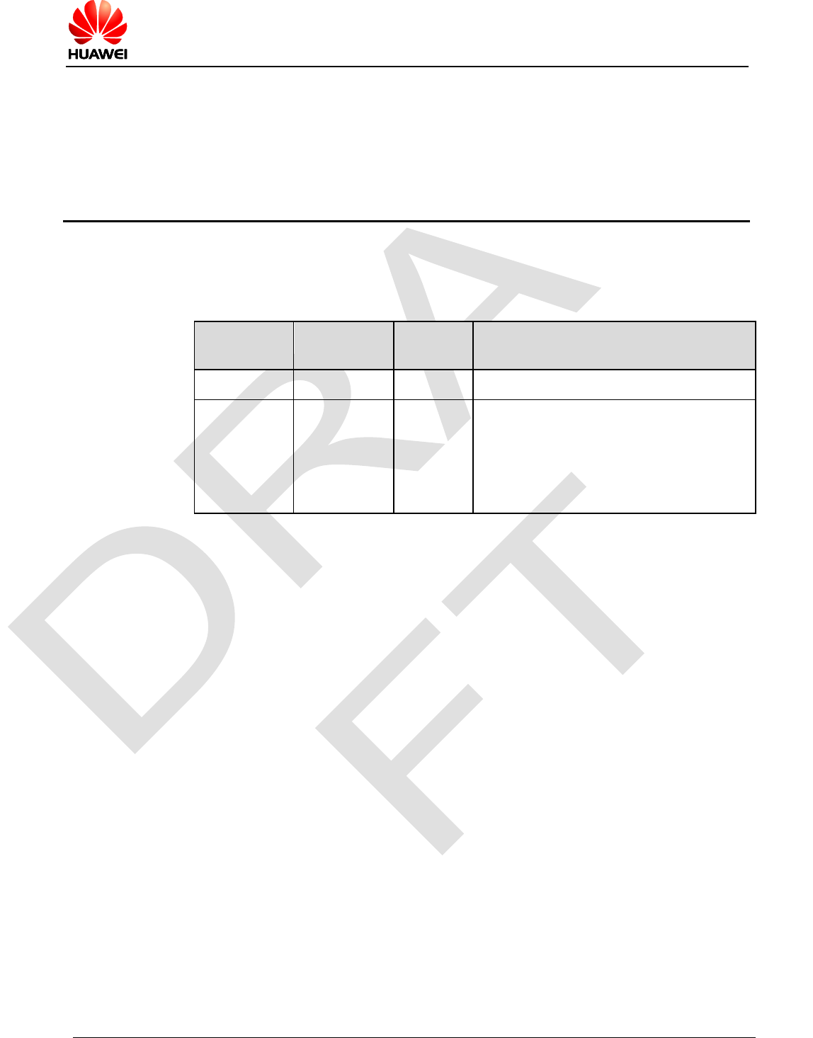
01 2017-03-23 - Draft release
02 2017-05-26 - 1.Cancel SPI/I2C function;
2.Cancel wake_up out function, use
RING to replace it;
3.Update the pin map interface picture
because the change above.
Huawei Proprietary and Confidential
Copyright © Huawei Technologies Co., Ltd. 3
HUAWEI ME309-562 eMTC LGA Module
Hardware Guide
Contents
1 Introduction.................................................................................................................................... 5
2 Overall Description ...................................................................................................................... 6
2.1 About This Chapter ........................................................................................................................... 6
2.2 Function Overview............................................................................................................................ 6
2.3 Circuit Block Diagram ....................................................................................................................... 7
2.4 Application Block Diagram ............................................................................................................... 8
3 Description of the Application Interfaces .............................................................................. 10
3.1 About This Chapter ......................................................................................................................... 10
3.2 LGA Interface ................................................................................................................................. 10
4 Mechanical Specifications ......................................................................................................... 20
4.1 About This Chapter ......................................................................................................................... 20
4.2 Storage Requirement ..................................................................................................................... 20
4.3 Moisture Sensitivity ........................................................................................................................ 20
4.4 Dimensions ..................................................................................................................................... 20
4.5 Customer PCB Design ................................................................................................................... 22
4.5.1 PCB Surface Finish ............................................................................................................... 22
4.5.2 PCB Pad Design .................................................................................................................... 22
4.5.3 Solder Mask ........................................................................................................................... 24
4.5.4 Requirements on PCB Layout ............................................................................................... 24
4.5.5 Stencil Design ........................................................................................................................ 24
Huawei Proprietary and Confidential
Copyright © Huawei Technologies Co., Ltd. 4
HUAWEI ME309-562 eMTC LGA Module
Hardware Guide
1 Introduction
This document describes the hardware application interfaces and air interfaces
provided by HUAWEI ME309-562 eMTC LGA module (hereinafter referred to as the
ME309-562 module).
This document helps hardware engineer to understand the interface specifications,
electrical features and related product information of the ME309-562 module.
Huawei Proprietary and Confidential
Copyright © Huawei Technologies Co., Ltd. 5
HUAWEI ME309-562 eMTC LGA Module
Hardware Guide
2 Overall Description
2.1 About This Chapter
This chapter gives a general description of the ME309-562 module and provides:
Function Overview
Circuit Block Diagram
Application Block Diagram
2.2 Function Overview
Table 2-1 ME309-562 module features
Feature Description
Physical
Dimensions
Dimensions (W × L × H): 18 mm × 24 mm × 2.5 mm
Weight TBD
Operating
Bands
HD-FDD LTE: Band 2, Band 4, Band 12, Band13
Operating
Temperature Normal operating temperature: –30°C to +75°C (Characteristics
guaranteed)
Extended operating temperature[1]: –40°C to +85°C (Normal
working)
Storage
Temperature –40°C to +95°C
Power
Voltage 3.3 V to 4.2 V (3.8 V is recommended.)
Huawei Proprietary and Confidential
Copyright © Huawei Technologies Co., Ltd. 6
HUAWEI ME309-562 eMTC LGA Module
Hardware Guide
Feature Description
Application
Interface
(120-pin LGA
interface)
GPIO x 5
UART interface (one 8-wire UART0, two 4-wire UART1&UART2,
and UART2 is only for debugging)
Standard SIM interface
ADC interface x 2
SPI interface (software not support)
I2C interface (software not support)
LED interface x 2
JTAG interface
Power supply interface
Power on/off interface
Hardware reset interface
Wake in/out interface
Antenna
Interface RF antenna pad x 1
Data Services LTE FDD: DL 300kbps; UL 375kbps @1.4MHz BW catM1
[1]: When the ME309-562 module works at –40°C to –30°C or +75°C to +85°C, NOT all its
RF performances comply with the 3GPP specifications.
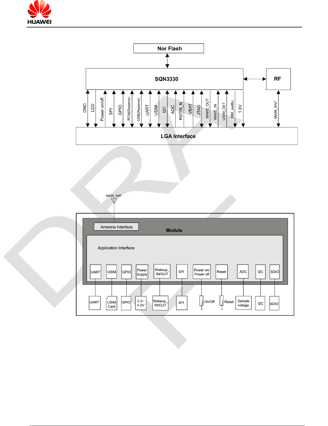
2.3 Circuit Block Diagram
Figure 2-1 shows the circuit block diagram of the ME309-562 module. The major
functional units of the ME309-562 module contain the following parts:
Baseband controller
Nor flash
RF Circuit
Huawei Proprietary and Confidential
Copyright © Huawei Technologies Co., Ltd. 7
HUAWEI ME309-562 eMTC LGA Module
Hardware Guide
Figure 2-1 Circuit block diagram of the ME309-562 module
2.4 Application Block Diagram
Figure 2-2 Application block diagram of the ME309-562 module
UART Interface: The module supports 3 UART interfaces. Two are 4-wire
UARTs, and the other one is 8-wire UART. Uart02 is only for
debugging.
SIM Interface: The SIM interface provides the interface for a SIM card.
GPIO: General Purpose I/O pins.
External Power
Supply: DC 3.8 V is recommended.
ADC: Analog-to-Digital Converter
I2C: Inter-Integrated Circuit
Huawei Proprietary and Confidential
Copyright © Huawei Technologies Co., Ltd. 8
HUAWEI ME309-562 eMTC LGA Module
Hardware Guide
SPI: Serial Peripheral Interface
RF Pad: RF antenna interface.
Huawei Proprietary and Confidential
Copyright © Huawei Technologies Co., Ltd. 9
HUAWEI ME309-562 eMTC LGA Module
Hardware Guide
3 Description of the Application Interfaces
3.1 About This Chapter
This chapter mainly describes the external application interfaces of the ME309-562
module LGA Interface.
3.2 LGA Interface
The ME309-562 module uses a 120-pin LGA as its external interface. For details
about the module and dimensions, see 4.4 Dimensions.
Huawei Proprietary and Confidential
Copyright © Huawei Technologies Co., Ltd. 10
HUAWEI ME309-562 eMTC LGA Module
Hardware Guide
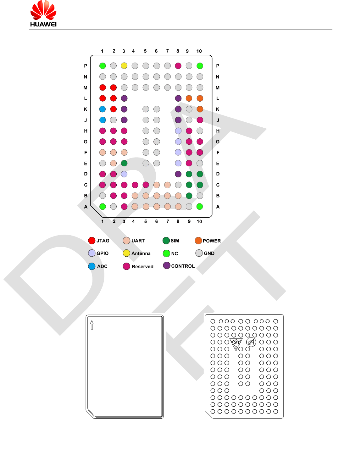
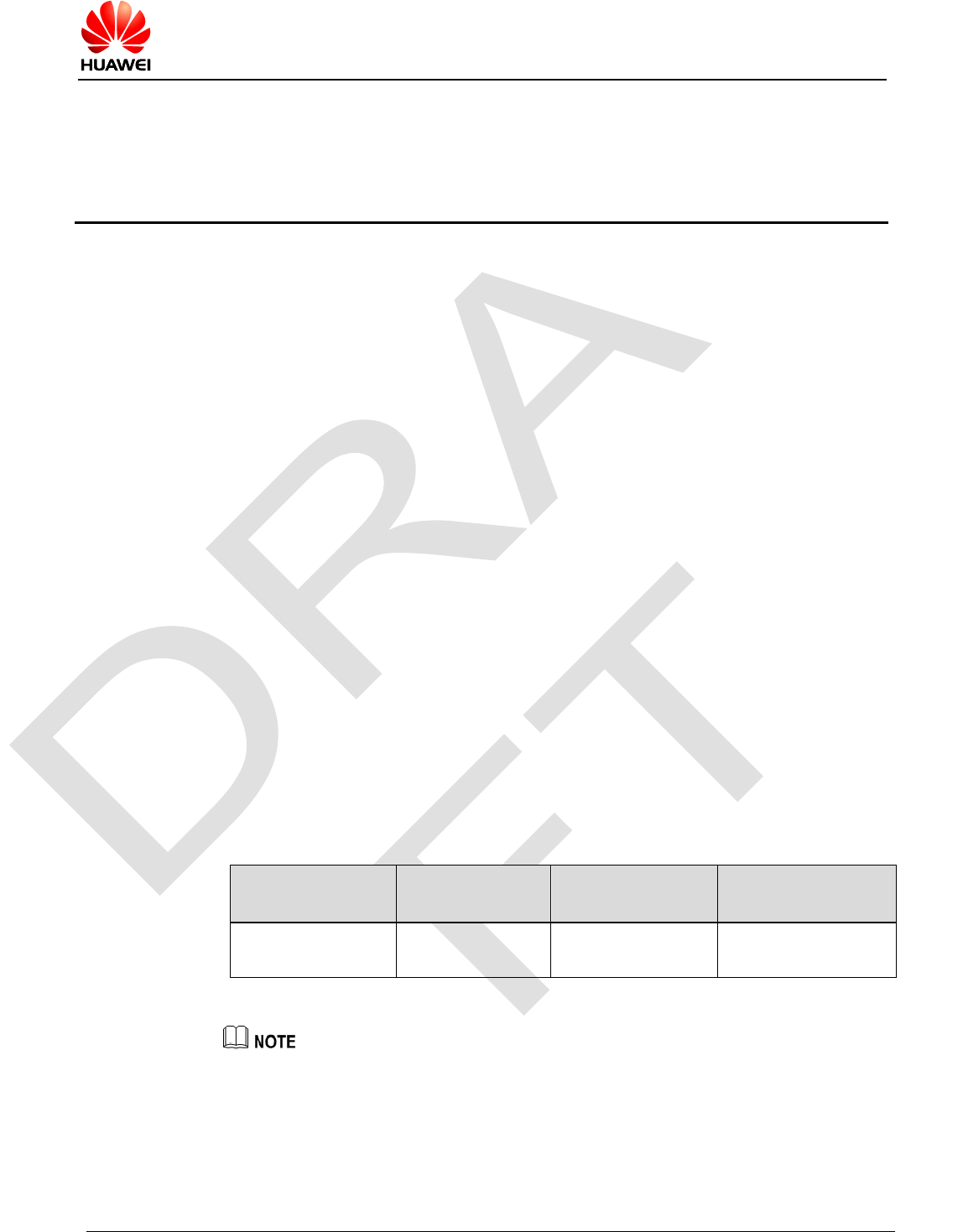
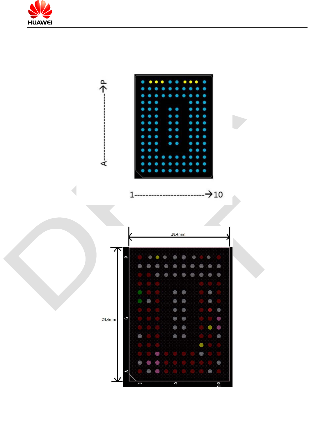
Figure 3-1 Pin map of LGA interface (Top view)
Update 26/05/2017
Figure 3-2 Appearance of ME309-562 module (without label)
Top View
Huawei Proprietary and Confidential
Copyright © Huawei Technologies Co., Ltd. 11
HUAWEI ME309-562 eMTC LGA Module
Hardware Guide
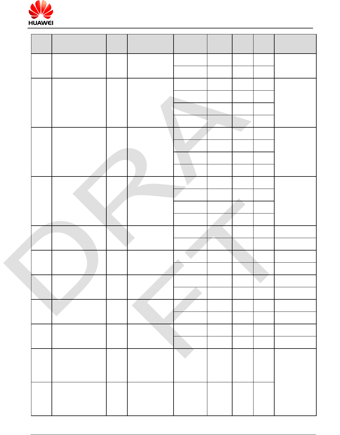
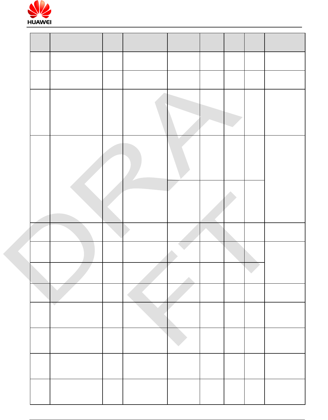
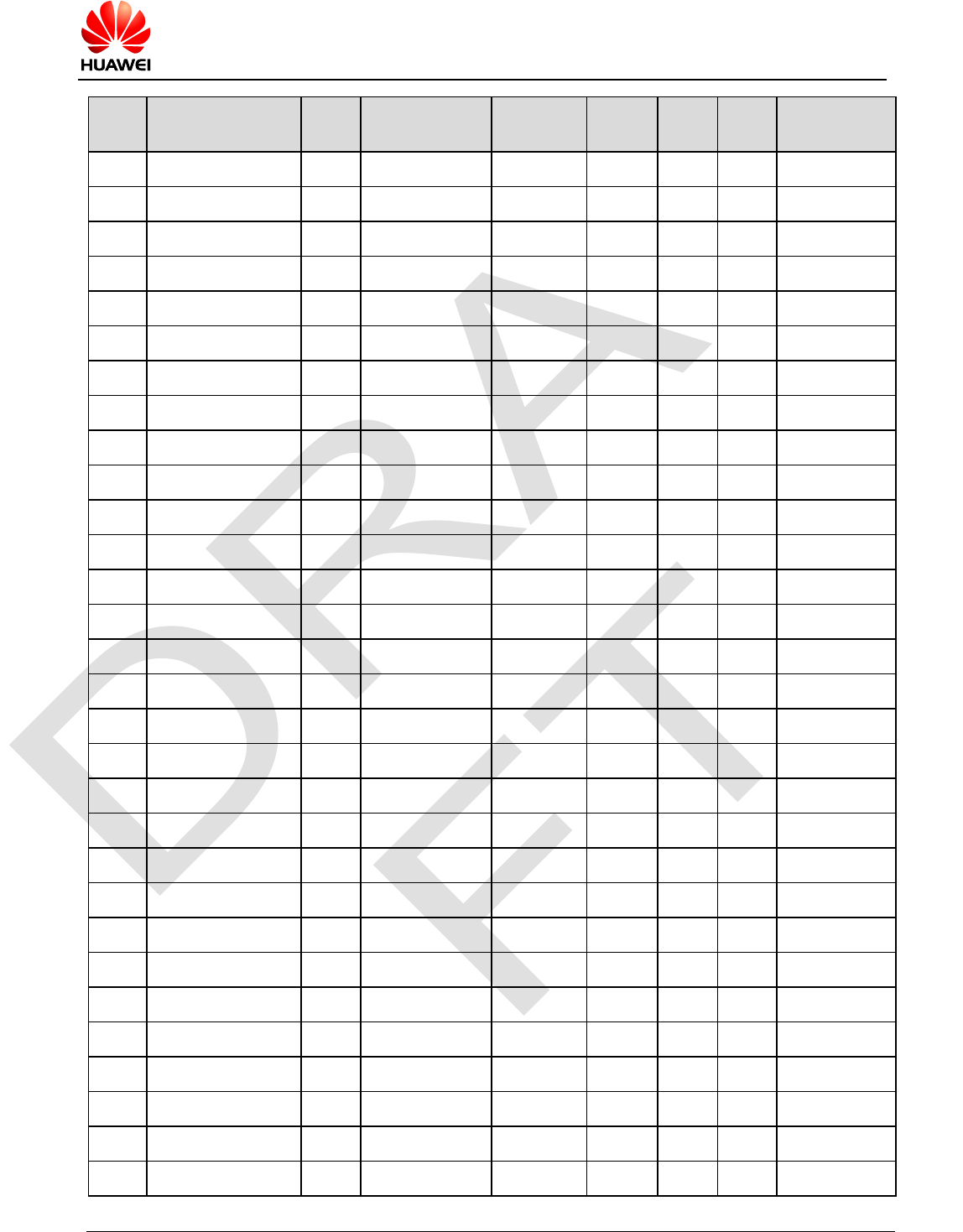
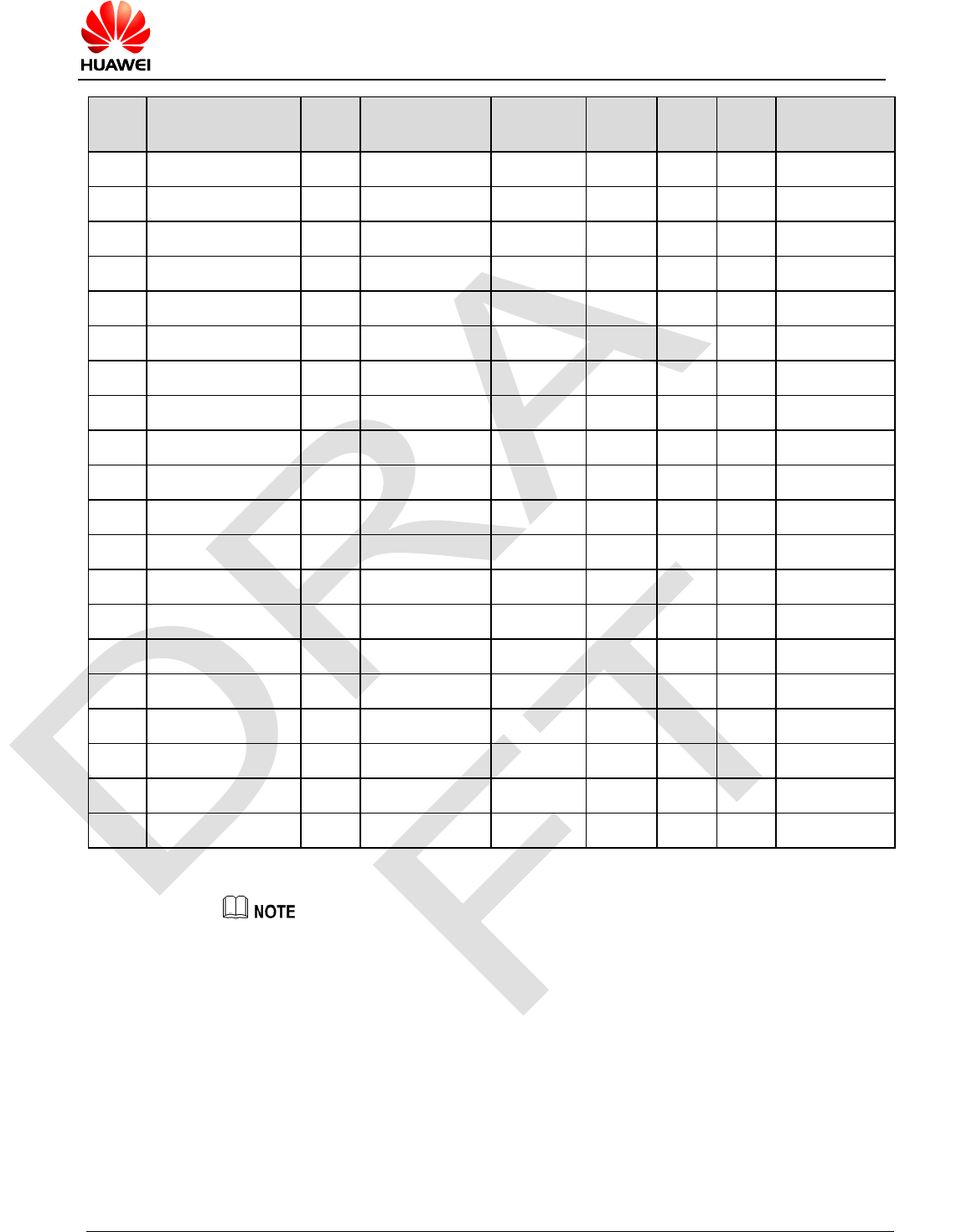
Table 3-1 Definitions of pins on the LGA interface
Pin
No.
Pin Name Pad
Type
Description Parameter Min.
(V)
Typ.
(V)
Max.
(V)
Comments
A8 UART0_TX O UART0 transmit
output
VOH 1.44 1.8 1.8 -
VOL 0 - 0.36 -
A7 UART0_RX I UART0 receive
data input
VIH 1.26 1.8 1.8 -
VIL 0 - 0.54 -
B7 UART0_CTS I UART0 clear to
send
VIH 1.26 1.8 1.8 -
VIL 0 - 0.54 -
B8 UART0_RTS O UART0 ready
for
receive
VOH 1.44 1.8 1.8 -
VOL 0 - 0.36 -
C7 UART0_DTR I Data terminal
ready
VIH 1.26 1.8 1.8 -
VIL 0 - 0.54 -
C6 UART0_DSR O UART0 data set
ready
VOH 1.44 1.8 1.8 -
VOL 0 - 0.36 -
B6 UART0_DCD O UART0 data
carrier detect
VOH 1.44 1.8 1.8 -
VOL 0 - 0.36 -
A6 UART0_RING O UART0 ring
indicator
VOH 1.44 1.8 1.8 Use as
wake_up out
VOL 0 - 0.36
A4 UART1_TX O UART1 transmit
output
VOH 1.44 1.8 1.8 -
VOL 0 - 0.36 -
A5 UART1_RX I UART1 receive
data input
VIH 1.26 1.8 1.8 -
VIL 0 - 0.54 -
B4 UART1_CTS I UART1 clear to
send
VIH 1.26 1.8 1.8 -
VIL 0 - 0.54 -
B5 UART1_RTS O UART1 ready
for
receive
VOH 1.44 1.8 1.8 -
VOL 0 - 0.36 -
F3 UART2_TX O UART2 transmit
output
VOH 1.44 1.8 1.8 -
VOL 0 - 0.36 -
F1 UART2_RX I UART2 receive
data input
VIH 1.26 1.8 1.8 -
VIL 0 - 0.54 -
Huawei Proprietary and Confidential
Copyright © Huawei Technologies Co., Ltd. 12
HUAWEI ME309-562 eMTC LGA Module
Hardware Guide
Pin
No.
Pin Name Pad
Type
Description Parameter Min.
(V)
Typ.
(V)
Max.
(V)
Comments
F2 UART2_CTS I UART2 clear to
send
VIH 1.26 1.8 1.8 -
VIL 0 - 0.54 -
E2 UART2_RTS O UART2 ready
for
receive
VOH 1.44 1.8 1.8 -
VOL 0 - 0.36 -
D1 SPI_CS_N O Active low chip
select to SPI
device
VOH 1.44 1.8 1.8 NOT support
VOL 0 - 0.36
D2 SPI_CLK O Clock to SPI
device, running
at 104MHz
VOH 1.44 1.8 1.8 NOT support
VOL 0 - 0.36
C2 SPI_MOSI O Serial data line
for transmitted
data, master out
VOH 1.44 1.8 1.8 NOT support
VOL 0 - 0.36
C1 SPI_MISO I Serial data line
for received
data, master in
VIH 1.26 1.8 1.8 NOT support
VIL 0 - 0.54
G1 I2C_SCL O I2C bus serial
clock line (need
pull up to
VCC_EXT)
VOH 1.44 1.8 1.8 NOT support
VOL 0 - 0.36
H1 I2C_SDA I/O I2C bus serial
data line (need
pull up to
VCC_EXT)
VOH 1.44 1.8 1.8 NOT support
VOL 0 - 0.36
VIH 1.26 1.8 1.8
VIL 0 - 0.54
D9 SIM_VCC PO Power supply for
SIM
- - 1.8/
3.0
- -
D10 SIM_IO I/O SIM data - - 1.8/
3.0
- -
B9 SIM_CLK O SIM clock - - 1.8/
3.0
- -
C9 SIM_RST O SIM reset - - 1.8/
3.0
- -
C10 SIM_DETECT I SIM hot swap VIH 1.26 1.8 1.8 If not use,
please pull it
Huawei Proprietary and Confidential
Copyright © Huawei Technologies Co., Ltd. 13
HUAWEI ME309-562 eMTC LGA Module
Hardware Guide
Pin
No.
Pin Name Pad
Type
Description Parameter Min.
(V)
Typ.
(V)
Max.
(V)
Comments
detection
H: SIM is resent
L: SIM is absent
VIL
0 - 0.54 high to
VCC_EXT on
your board.
E3 SIM_SWITCH O Switch from one
card to the
other, should
cooperate with
SIM switch IC
chip.
VOH 1.44 1.8 1.8 If not use,
please leave it
open.
VOL 0 - 0.36
L8 WAKEUP_IN I The host sets
the module into
sleep mode or
wakes up the
module from
sleep mode.
H: Sleep mode
is disabled.
L: Sleep mode is
enabled.
(default L )
VIH 1.26 1.8 1.8 -
VIL 0 - 0.54 -
L3 WAKEUP_OUT O Module wakes
up the host
VOH 1.44 1.8 1.8 NOT support,
please use
RING as
wake_up out
VOL 0 - 0.36
K3 SLEEP_STATUS O Sleep status
indicator
H: The module
is in wakeup
state.
L: The module is
in sleep state.
VOH 1.44 1.8 1.8 -
VOL 0 - 0.36 -
J8 LED_MODE O Network mode
indicator.
VOH 1.44 1.8 1.8 -
VOL 0 - 0.36 -
E8 GPIO1 I/O General
Purpose I/O
pins.
VOH 1.44 1.8 1.8 Default
configuration
is input pull
down.
VOL 0 - 0.36
VIH VIH 1.26 1.8
VIL VIL 0 -
G8 GPIO2 I/O General
Purpose I/O
VOH 1.44 1.8 1.8 Default
configuration
is input pull
VOL 0 - 0.36
Huawei Proprietary and Confidential
Copyright © Huawei Technologies Co., Ltd. 14
HUAWEI ME309-562 eMTC LGA Module
Hardware Guide
Pin
No.
Pin Name Pad
Type
Description Parameter Min.
(V)
Typ.
(V)
Max.
(V)
Comments
pins. VIH VIH 1.26 1.8 down.
VIL VIL 0 -
D3 GPIO3 I/O General
Purpose I/O
pins.
VOH 1.44 1.8 1.8 Default
configuration
is input pull
down.
VOL 0 - 0.36
VIH VIH 1.26 1.8
VIL VIL 0 -
F8 GPIO4 I/O General
Purpose I/O
pins.
VOH 1.44 1.8 1.8 Default
configuration
is input pull
down.
VOL 0 - 0.36
VIH VIH 1.26 1.8
VIL VIL 0 -
H8 GPIO5 I/O General
Purpose I/O
pins.
VOH 1.44 1.8 1.8 Default
configuration
is input pull
down.
VOL 0 - 0.36
VIH VIH 1.26 1.8
VIL VIL 0 -
L2 JTAG_TMS I JTAG test mode
select
VIH 1.26 1.8 1.8 -
VIL 0 - 0.54 -
M2 JTAG_TRST_N I JTAG test reset VIH 1.26 1.8 1.8 -
VIL 0 - 0.54 -
K2 JTAG_TCK I JTAG test clock VIH 1.26 1.8 1.8 -
VIL 0 - 0.54 -
L1 JTAG_TDO O JTAG test data
output
VOH 1.44 1.8 1.8 -
VOL 0 - 0.36 -
M1 JTAG_TDI I JTAG test serial
data input
VIH 1.26 1.8 1.8 -
VIL 0 - 0.54 -
K1 ADC_1 AI Conversion
interface for
analog signals
to digital signals
- -0.036 - 1.836 The ADC’s
resolution is
10bit
J1 ADC_2 AI Conversion
interface for
analog signals
to digital signals
- -0.036 - 1.836
Huawei Proprietary and Confidential
Copyright © Huawei Technologies Co., Ltd. 15
HUAWEI ME309-562 eMTC LGA Module
Hardware Guide
Pin
No.
Pin Name Pad
Type
Description Parameter Min.
(V)
Typ.
(V)
Max.
(V)
Comments
D8 POWER_ON I System power -
on
- - 1.8 - Not support,
will cancel it
J3 POWER_OFF I System power -
off
- - 1.8 - Not support,
will cancel it
F9 RESIN_N I System reset,
active low.
- - 1.8 - Please add a
pull-high
resister to
1.8V on your
board (not
VCC_EXT).
K8 BOOT_MODE I Boot mode
configure
H: boot from
flash
L: boot from
host
VIH 1.26 1.8 1.8 Please design
a pull-high
resister to
VCC_EXT and
a pull down
resister to
Ground on
your board,
default pull
high resister is
on the PCB
board.
VIL 0 - 0.54
K10 VCC_EXT PO Pin for external
power output
- 1.71 1.8 1.89 Max current is
10mA
L9 VCC_Module PI Power supply
Input
- 3.3 3.8 4.2 Max current is
about 300mA
L10 VCC_Module PI Power supply
input
- 3.3 3.8 4.2
P3 RF_ANT RF RF pin of
module
- - - - -
A3 Reserved - Reserved,
please keep this
pin open.
- - - - -
B2 Reserved - Reserved,
please keep this
pin open.
- - - - -
B3 Reserved - Reserved,
please keep this
pin open.
- - - - -
C3 Reserved - Reserved,
please keep this
pin open.
- - - - -
Huawei Proprietary and Confidential
Copyright © Huawei Technologies Co., Ltd. 16
HUAWEI ME309-562 eMTC LGA Module
Hardware Guide
Pin
No.
Pin Name Pad
Type
Description Parameter Min.
(V)
Typ.
(V)
Max.
(V)
Comments
G9 Reserved - Reserved,
please keep this
pin open.
- - - - -
G10 Reserved - Reserved,
please keep this
pin open.
- - - - -
F10 Reserved - Reserved,
please keep this
pin open.
- - - - -
E9 Reserved - Reserved,
please keep this
pin open.
- - - - -
J10 Reserved - Reserved,
please keep this
pin open.
- - - - -
H9 Reserved - Reserved,
please keep this
pin open.
- - - - -
C5 Reserved - Reserved,
please keep this
pin open.
- - - - -
G2 Reserved - Reserved,
please keep this
pin open.
- - - - -
G3 Reserved - Reserved,
please keep this
pin open.
- - - - -
H2 Reserved - Reserved,
please keep this
pin open.
- - - - -
H3 Reserved - Reserved,
please keep this
pin open.
- - - - -
P8 Reserved - Reserved,
please keep this
pin open.
- - - - -
C4 Reserved - Reserved,
please keep this
pin open.
- - - - -
A1 NC - Not connected - - - - -
Huawei Proprietary and Confidential
Copyright © Huawei Technologies Co., Ltd. 17
HUAWEI ME309-562 eMTC LGA Module
Hardware Guide
Pin
No.
Pin Name Pad
Type
Description Parameter Min.
(V)
Typ.
(V)
Max.
(V)
Comments
A10 NC - Not connected - - - - -
P1 NC - Not connected - - - - -
P10 NC - Not connected - - - - -
A2 GND - Ground - - - - -
A9 GND - Ground - - - - -
B1 GND - Ground - - - - -
B10 GND - Ground - - - - -
C8 GND - Ground - - - - -
E1 GND - Ground - - - - -
E5 GND - Ground - - - - -
E6 GND - Ground - - - - -
E10 GND - Ground - - - - -
F5 GND - Ground - - - - -
F6 GND - Ground - - - - -
G5 GND - Ground - - - - -
G6 GND - Ground - - - - -
H5 GND - Ground - - - - -
H6 GND - Ground - - - - -
H10 GND - Ground - - - - -
J2 GND - Ground - - - - -
J5 GND - Ground - - - - -
J6 GND - Ground - - - - -
J9 GND - Ground - - - - -
K5 GND - Ground - - - - -
K6 GND - Ground - - - - -
K9 GND - Ground - - - - -
M3 GND - Ground - - - - -
M4 GND - Ground - - - - -
M5 GND - Ground - - - - -
M6 GND - Ground - - - - -
Huawei Proprietary and Confidential
Copyright © Huawei Technologies Co., Ltd. 18
HUAWEI ME309-562 eMTC LGA Module
Hardware Guide
Pin
No.
Pin Name Pad
Type
Description Parameter Min.
(V)
Typ.
(V)
Max.
(V)
Comments
M7 GND - Ground - - - - -
M8 GND - Ground - - - - -
M9 GND - Ground - - - - -
M10 GND - Ground - - - - -
N1 GND - Ground - - - - -
N2 GND - Ground - - - - -
N3 GND - Ground - - - - -
N4 GND - Ground - - - - -
N5 GND - Ground - - - - -
N6 GND - Ground - - - - -
N7 GND - Ground - - - - -
N8 GND - Ground - - - - -
N9 GND - Ground - - - - -
N10 GND - Ground - - - - -
P2 GND - Ground - - - - -
P4 GND - Ground - - - - -
P5 GND - Ground - - - - -
P6 GND - Ground - - - - -
P7 GND - Ground - - - - -
P9 GND - Ground - - - - -
I indicates pins for digital signal input; O indicates pins for digital signal output; AI indicates
pins for analog signal input; PI indicates power input pins; PO indicates power output pins;
P indicates power pins.
VIL indicates low-level input voltage; VIH indicates high-level input voltage; VOL indicates low-
level output voltage; VOH indicates high-level output voltage.
The NC (Not Connected) pins are floating and there are no signal connected to these pins.
The Reserved pins are internally connected to the module. Therefore, these pins should
not be used, otherwise they may cause problems. Please contact with us for more details
about this information.
Huawei Proprietary and Confidential
Copyright © Huawei Technologies Co., Ltd. 19
HUAWEI ME309-562 eMTC LGA Module
Hardware Guide
4 Mechanical Specifications
4.1 About This Chapter
Storage Requirement
Moisture Sensitivity
Dimensions
Customer PCB Design
4.2 Storage Requirement
The module must be stored and sealed properly in vacuum package under a
temperature below 40°C and the relative humidity less than 90% in order to ensure
the weldability within 12 months.
4.3 Moisture Sensitivity
The moisture sensitivity is level 3.
After unpacking, the module must be assembled within 168 hours under the
environmental conditions that the temperature is lower than 30°C and the
relative humidity is less than 60%. If the preceding conditions cannot be met, the
module needs to be baked according to the parameters specified in Table 4-1 .
Table 4-1 Baking parameters
Baking
Temperature
Baking
Condition
Baking Duration Remarks
125°C±5°C Relative humidity
≤ 60% 8 hours Refer to JESD-033C
in detail
Moving, storing, and processing the product must comply with IPC/JEDEC J-STD-033.
4.4 Dimensions
Figure 4-1 shows the dimensions of the ME309-562 module in details.
Huawei Proprietary and Confidential
Copyright © Huawei Technologies Co., Ltd. 20
HUAWEI ME309-562 eMTC LGA Module
Hardware Guide
Figure 4-1 Dimensions (Unit: mm)
The detail information about the corner and the module pin description top view:
1. the yellow pins, diameter is 0.76 mm, pitch is 1.35 mm,
2. the blue pins, diameter is 0.89 mm, pitch is 1.60 mm.
Huawei Proprietary and Confidential
Copyright © Huawei Technologies Co., Ltd. 21
HUAWEI ME309-562 eMTC LGA Module
Hardware Guide
4.5 Customer PCB Design
4.5.1 PCB Surface Finish
The PCB surface finish recommended is Electroless Nickel Immersion Gold (ENIG).
Organic Solderability Preservative (OSP) may also be used, ENIG preferred.
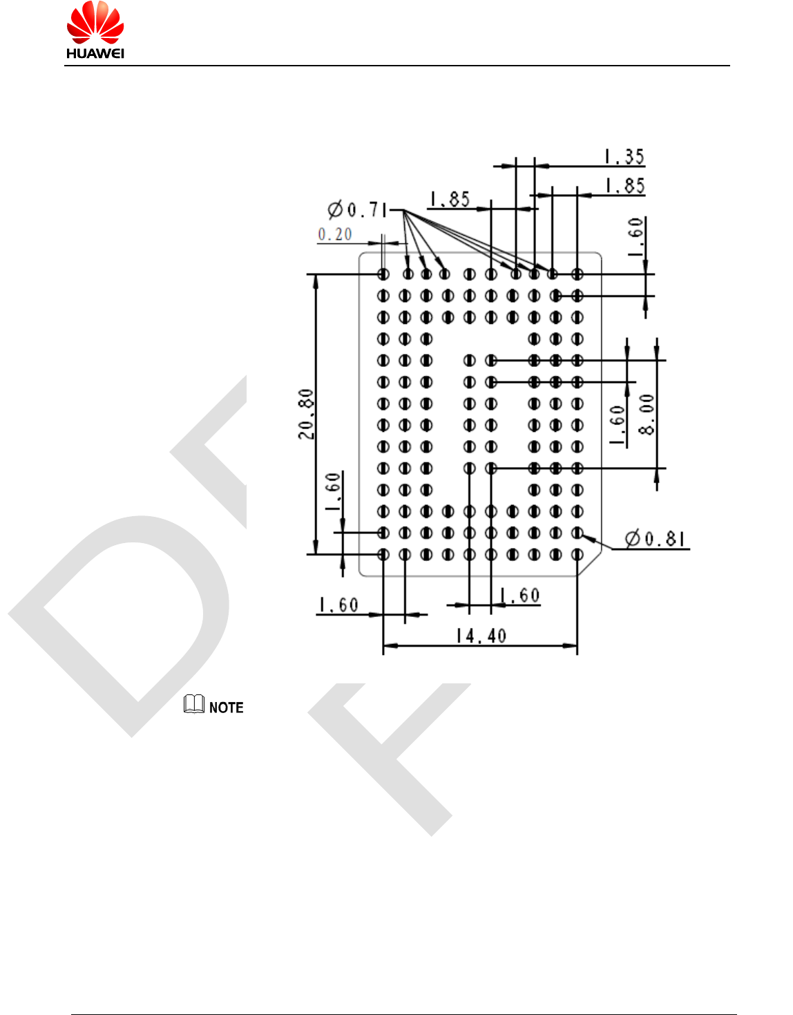
4.5.2 PCB Pad Design
To achieve assembly yields and solder joints of high reliability, it is recommended that
the PCB pad size be designed as follows:
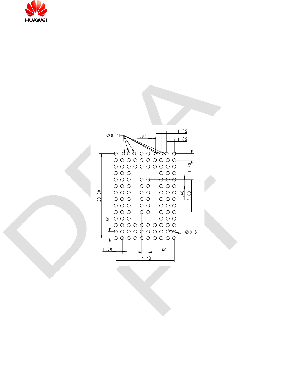
Figure 4-2 Footprint design of customer's PCB (Unit: mm)
Huawei Proprietary and Confidential
Copyright © Huawei Technologies Co., Ltd. 22
HUAWEI ME309-562 eMTC LGA Module
Hardware Guide
Some detail information about the recommend module footprint:
1. the yellow pins, diameter is 0.71 mm, pitch is 1.35 mm,
2. the blue pins, diameter is 0.81 mm, pitch is 1.60 mm.
Figure 4-3 Detail information about the recommend module footprint
Figure 4-4 Recommended Package Size on HUAWEI motherboard (Unit: mm)
Huawei Proprietary and Confidential
Copyright © Huawei Technologies Co., Ltd. 23

HUAWEI ME309-562 eMTC LGA Module
Hardware Guide
4.5.3 Solder Mask
Non Solder Mask Defined (NSMD) is recommended. In addition, the solder mask of
the NSMD pad design is larger than the pad so the reliability of the solder joint can be
improved.
The solder mask must be 100 µm–150 µm larger than the pad, that is, the single side
of the solder mask must be 50 µm–75 µm larger than the pad. The specific size
depends on the processing capability of the PCB manufacturer.
4.5.4 Requirements on PCB Layout
To reduce deformation, a thickness of at least 1.0 mm is recommended.
Other devices must be located more than 3 mm (5 mm recommended) away
from the two parallel sides of the LGA module (rework requirement),and other
sides with 0.6 mm. The minimum distance between the LGA module and the
PCB edge is 0.3 mm.
When the PCB layout is double sided, the LGA module must be placed on the
second side for assembly; so as to avoid module dropped from PCB or
component (located in module) re-melding defects caused by uneven weight.
Customers PCB together with ME309-562 should be placed in an enclosed box
to reduce the impact of high humidity as far as possible.
The bottom of the module is not allowed to put non-ground line or non-ground
hole. If the design can not be achieved, then the non-gound line and hole must
be covered by green oil.
4.5.5 Stencil Design
It is recommended that the stencil for the LGA module be 0.15 mm in thickness. The
stencil design is shown as Figure 4-5 :
Huawei Proprietary and Confidential
Copyright © Huawei Technologies Co., Ltd. 24
HUAWEI ME309-562 eMTC LGA Module
Hardware Guide
Figure 4-5 Recommended stencil design of LGA module (Unit: mm)
The stencil design has been qualified for HUAWEI motherboard assembly, customers can
adjust the parameters by their motherboard design and process situation to assure LGA
soldering quality and no defect.
Huawei Proprietary and Confidential
Copyright © Huawei Technologies Co., Ltd. 25