Huawei MU736 HSPA M.2 Module Hardware Guide (V100R001 05, English)
HUAWEI MU736 HSPA+ M.2 Module Hardware Guide-(V100R001_05, English)
2014-01-21
User Manual: Huawei
Open the PDF directly: View PDF ![]() .
.
Page Count: 81
- Revision History
- 1 Introduction
- 2 Overall Description
- 3 Description of the Application Interfaces
- 3.1 About This Chapter
- 3.2 75-pin Gold Finger
- 3.3 Power Interface
- 3.4 Signal Control Interface
- 3.4.1 Overview
- 3.4.2 Power_On_Off Control Pin
- Table 3-4 Two states of Power_On_Off
- MU736 is powered by regulated 3.3 V
- MU736 is powered directly to battery
- 3.4.3 RESET# Pins
- 3.4.4 LED# Pin
- 3.4.5 W_DISABLE# Pin
- 3.4.6 GPS_DISABLE# Pin
- 3.4.7 Wake_On_WWAN# Pin
- 3.4.8 BodySAR_N Pin
- 3.4.9 SIM_DET Pin
- 3.5 USB Interface
- 3.6 USIM Card Interface
- 3.7 Tunable Antenna Control
- 3.8 Config Pins
- 3.9 NC Pins
- 3.10 RF Antenna Interface
- 3.10.1 RF Connector location
- 3.10.2 Coaxial RF Connector Guidelines
- Figure 3-27 RF connector dimensions
- Table 3-16 The major specifications of the RF connector
- Figure 3-28 Specifications of 0.81 mm coaxial cable mating with the RF connector
- Figure 3-29 Connection between the RF connector and the 0.81 mm cable
- Figure 3-30 Specifications of 1.13 mm coaxial cable mating with the RF connector
- Figure 3-31 Connection between the RF connector and the 1.13 mm cable
- 4 RF Specifications
- 5 Electrical and Reliability Features
- 5.1 About This Chapter
- 5.2 Absolute Ratings
- 5.3 Operating and Storage Temperatures and Humidity
- 5.4 Electrical Features of Application Interfaces
- 5.5 Power Supply Features
- 5.5.1 Input Power Supply
- 5.5.2 Power Consumption
- Table 5-8 Averaged power off DC power consumption of MU736
- Table 5-9 Averaged standby DC power consumption of MU736 (WCDMA/HSDPA/GSM)
- Table 5-10 Averaged Data Transmission DC power consumption of MU736 (WCDMA/HSDPA)
- Table 5-11 Averaged DC power consumption of MU736 (GPRS/EDGE)
- Table 5-12 Averaged GPS operation DC power consumption of MU736
- 5.6 Reliability Features
- 5.7 EMC and ESD Features
- 6 Mechanical Specifications
- 7 Installation
- 7.1 About This Chapter
- 7.2 Connect MU736 to Board
- 7.3 Antenna Plug
- Figure 7-2 Mating the plug
- 1. Align the mating tool or the mating end of the tool over the plug end of the cable assembly.
- 2. Firmly place the tool over the plug until it is secured in the tool.
- 3. Place the plug cable assembly (held in the tool) over the corresponding receptacle.
- 4. Assure that the plug and receptacle are aligned press-down perpendicular to the mounting surface until both connectors are fully mated.
- 5. Remove the mating tool by pulling it up carefully.
- 8 Certifications
- 9 Safety Information
- 9.1 Interference
- 9.2 Medical Device
- 9.3 Area with Inflammables and Explosives
- 9.4 Traffic Security
- 9.5 Airline Security
- 9.6 Safety of Children
- 9.7 Environment Protection
- 9.8 WEEE Approval
- 9.9 RoHS Approval
- 9.10 Laws and Regulations Observance
- 9.11 Care and Maintenance
- 9.12 Emergency Call
- 9.13 Regulatory Information
- 10 Appendix A Circuit of Typical Interface
- 11 Appendix B Acronyms and Abbreviations

HUAWEI MU736 HSPA+ M.2 Module
Hardware Guide
Issue
05
Date
2014-01-14

Huawei Technologies Co., Ltd. provides customers with comprehensive technical support and service. For
any assistance, please contact our local office or company headquarters.
Huawei Technologies Co., Ltd.
Huawei Industrial Base, Bantian, Longgang, Shenzhen 518129, People’s Republic of China
Tel: +86-755-28780808 Global Hotline: +86-755-28560808 Website: www.huawei.com
E-mail: mobile@huawei.com
Please refer color and shape to product. Huawei reserves the right to make changes or improvements to any
of the products without prior notice.
Copyright © Huawei Technologies Co., Ltd. 2014. All rights reserved.
No part of this document may be reproduced or transmitted in any form or by any means without prior written
consent of Huawei Technologies Co., Ltd.
The product described in this manual may include copyrighted software of Huawei Technologies Co., Ltd. and
possible licensors. Customers shall not in any manner reproduce, distribute, modify, decompile, disassemble,
decrypt, extract, reverse engineer, lease, assign, or sublicense the said software, unless such restrictions are
prohibited by applicable laws or such actions are approved by respective copyright holders under licenses.
Trademarks and Permissions
, , and
are trademarks or registered trademarks of Huawei Technologies Co., Ltd.
Other trademarks, product, service and company names mentioned are the property of their respective
owners.
Notice
Some features of the product and its accessories described herein rely on the software installed, capacities
and settings of local network, and may not be activated or may be limited by local network operators or
network service providers, thus the descriptions herein may not exactly match the product or its accessories
you purchase.
Huawei Technologies Co., Ltd. reserves the right to change or modify any information or specifications
contained in this manual without prior notice or obligation.
NO WARRANTY
THE CONTENTS OF THIS MANUAL ARE PROVIDED "AS IS". EXCEPT AS REQUIRED BY APPLICABLE
LAWS, NO WARRANTIES OF ANY KIND, EITHER EXPRESS OR IMPLIED, INCLUDING BUT NOT
LIMITED TO, THE IMPLIED WARRANTIES OF MERCHANTABILITY AND FITNESS FOR A PARTICULAR
PURPOSE, ARE MADE IN RELATION TO THE ACCURACY, RELIABILITY OR CONTENTS OF THIS
MANUAL.
TO THE MAXIMUM EXTENT PERMITTED BY APPLICABLE LAW, IN NO CASE SHALL HUAWEI
TECHNOLOGIES CO., LTD. BE LIABLE FOR ANY SPECIAL, INCIDENTAL, INDIRECT, OR
CONSEQUENTIAL DAMAGES, OR LOST PROFITS, BUSINESS, REVENUE, DATA, GOODWILL OR
ANTICIPATED SAVINGS.
Import and Export Regulations
Customers shall comply with all applicable export or import laws and regulations and will obtain all necessary
governmental permits and licenses in order to export, re-export or import the product mentioned in this
manual including the software and technical data therein.
HUAWEI MU736 HSPA+ M.2 Module
Hardware Guide
About This Document
Issue 05 (2014-01-14)
Huawei Proprietary and Confidential
Copyright © Huawei Technologies Co., Ltd.
3
About This Document
Revision History
Document
Version
Date
Chapter
Descriptions
01
2013-03-08
Creation
02
2013-05-09
3.7
Updated Tunable Antenna Control
4.4.2
Updated Table 4-4
4.5.1
Updated Antenna Design Indicators
4.5.3
Updated GSM/WCDMA/GPS Antenna
Requirements
5.5.2
Updated Table 5-9, Table 5-10
8.2
Updated Table 8-1
9.8
Updated WEEE Approval
9.9
Updated RoHS Approval
9.11
Updated Care and Maintenance
9.13
Deleted Specific Absorption Rate (SAR)
9.13
Updated Regulatory Information
03
2013-08-22
2.2
Updated Table 2-1 Features
3.2
Updated Table 3-1 Definitions of pins on
the M.2 interface
3.4.5
Added Figure 3-16 Connections of the
W_DISABLE# pin
3.4.6
Added Figure 3-17 Connections of the
GPS_DISABLE# pin
3.4.8
Updated Figure 3-20 Connections of the
BodySAR_N pin
3.4.9
Updated Figure 3-21 Connections of the
SIM_DET pin
HUAWEI MU736 HSPA+ M.2 Module
Hardware Guide
About This Document
Issue 05 (2014-01-14)
Huawei Proprietary and Confidential
Copyright © Huawei Technologies Co., Ltd.
4
Document
Version
Date
Chapter
Descriptions
3.7
Updated Table 3-11 List of ANTCTL pins
3.9
Updated Table 3-15 List of NC pins
5.2
Updated Table 5-1 Absolute ratings for the
MU736 module
5.5.2
Updated Table 5-12 DC power
consumption (GPS)
5.6
Updated Table 5-13 Test conditions and
results of the reliability of the MU736
module
6.2
Updated Figure 6-1 Dimensions of MU736
6.4
Updated Figure 6-4 Packet system
04
2013-10-21
5.6
Updated Table 5-13 Test conditions and
results of the reliability of the MU736
module
05
2014-01-14
5.5.2
Updated Power Consumption
5.7
Updated EMC and ESD Features

HUAWEI MU736 HSPA+ M.2 Module
Hardware Guide
Contents
Issue 05 (2014-01-14)
Huawei Proprietary and Confidential
Copyright © Huawei Technologies Co., Ltd.
5
Contents
1 Introduction .............................................................................................................................. 8
2 Overall Description .................................................................................................................. 9
2.1 About This Chapter...................................................................................................................... 9
2.2 Function Overview ...................................................................................................................... 9
2.3 Circuit Block Diagram ................................................................................................................. 11
3 Description of the Application Interfaces........................................................................... 12
3.1 About This Chapter.....................................................................................................................12
3.2 75-pin Gold Finger .....................................................................................................................12
3.3 Power Interface ..........................................................................................................................18
3.3.1 Overview ...........................................................................................................................18
3.3.2 Power Supply 3.3V Interface ..............................................................................................18
3.3.3 USIM Power Output UIM_PWR..........................................................................................20
3.4 Signal Control Interface ..............................................................................................................20
3.4.1 Overview ...........................................................................................................................20
3.4.2 Power_On_Off Control Pin .................................................................................................22
3.4.3 RESET# Pins.....................................................................................................................26
3.4.4 LED# Pin ...........................................................................................................................28
3.4.5 W_DISABLE# Pin ..............................................................................................................29
3.4.6 GPS_DISABLE# Pin ..........................................................................................................29
3.4.7 Wake_On_WWAN# Pin .....................................................................................................30
3.4.8 BodySAR_N Pin ................................................................................................................31
3.4.9 SIM_DET Pin .....................................................................................................................32
3.5 USB Interface.............................................................................................................................34
3.6 USIM Card Interface...................................................................................................................35
3.6.1 Overview ...........................................................................................................................35
3.6.2 Circuit Recommended for the USIM Card Interface ............................................................35
3.7 Tunable Antenna Control ............................................................................................................36
3.8 Config Pins ................................................................................................................................37
3.9 NC Pins .....................................................................................................................................38
3.10 RF Antenna Interface ...............................................................................................................38
3.10.1 RF Connector location .....................................................................................................38
3.10.2 Coaxial RF Connector Guidelines ....................................................................................39

HUAWEI MU736 HSPA+ M.2 Module
Hardware Guide
Contents
Issue 05 (2014-01-14)
Huawei Proprietary and Confidential
Copyright © Huawei Technologies Co., Ltd.
6
4 RF Specifications .................................................................................................................... 43
4.1 About This Chapter.....................................................................................................................43
4.2 Operating Frequencies ...............................................................................................................43
4.3 Conducted RF Measurement ......................................................................................................44
4.3.1 Test Environment ...............................................................................................................44
4.3.2 Test Standards ...................................................................................................................44
4.4 Conducted Rx Sensitivity and Tx Power .....................................................................................44
4.4.1 Conducted Receive Sensitivity ...........................................................................................44
4.4.2 Conducted Transmit Power ................................................................................................45
4.5 Antenna Design Requirements ...................................................................................................46
4.5.1 Antenna Design Indicators .................................................................................................46
4.5.2 Interference .......................................................................................................................49
4.5.3 GSM/WCDMA/GPS Antenna Requirements .......................................................................49
4.5.4 Radio Test Environment .....................................................................................................50
5 Electrical and Reliability Features ....................................................................................... 52
5.1 About This Chapter.....................................................................................................................52
5.2 Absolute Ratings ........................................................................................................................52
5.3 Operating and Storage Temperatures and Humidity ....................................................................53
5.4 Electrical Features of Application Interfaces ................................................................................53
5.5 Power Supply Features ..............................................................................................................54
5.5.1 Input Power Supply ............................................................................................................54
5.5.2 Power Consumption...........................................................................................................55
5.6 Reliability Features .....................................................................................................................60
5.7 EMC and ESD Features .............................................................................................................63
6 Mechanical Specifications .................................................................................................... 65
6.1 About This Chapter.....................................................................................................................65
6.2 Dimensions of MU736 ................................................................................................................65
6.3 Label ..........................................................................................................................................66
6.4 Packing System .........................................................................................................................68
7 Installation .............................................................................................................................. 70
7.1 About This Chapter.....................................................................................................................70
7.2 Connect MU736 to Board ...........................................................................................................70
7.3 Antenna Plug..............................................................................................................................71
8 Certifications ........................................................................................................................... 73
8.1 About This Chapter.....................................................................................................................73
8.2 Certifications ..............................................................................................................................73
9 Safety Information ................................................................................................................. 75
9.1 Interference ................................................................................................................................75
9.2 Medical Device ...........................................................................................................................75
9.3 Area with Inflammables and Explosives ......................................................................................75

HUAWEI MU736 HSPA+ M.2 Module
Hardware Guide
Contents
Issue 05 (2014-01-14)
Huawei Proprietary and Confidential
Copyright © Huawei Technologies Co., Ltd.
7
9.4 Traffic Security ...........................................................................................................................76
9.5 Airline Security ...........................................................................................................................76
9.6 Safety of Children.......................................................................................................................76
9.7 Environment Protection ..............................................................................................................76
9.8 WEEE Approval .........................................................................................................................76
9.9 RoHS Approval ..........................................................................................................................76
9.10 Laws and Regulations Observance ..........................................................................................77
9.11 Care and Maintenance .............................................................................................................77
9.12 Emergency Call ........................................................................................................................77
9.13 Regulatory Information .............................................................................................................77
9.13.1 CE Approval (European Union) ........................................................................................77
9.13.2 FCC Statement ................................................................................................................78
10 Appendix A Circuit of Typical Interface ........................................................................... 79
11 Appendix B Acronyms and Abbreviations ....................................................................... 80

HUAWEI MU736 HSPA+ M.2 Module
Hardware Guide
Introduction
Issue 05 (2014-01-14)
Huawei Proprietary and Confidential
Copyright © Huawei Technologies Co., Ltd.
8
1 Introduction
This document describes the hardware application interfaces and air interfaces that
are provided when HUAWEI MU736 HSPA+ M.2 Module (hereinafter referred to the
MU736 module) is used.
M.2 is the new name for NGFF (Next Generation Form Factor).
This document helps you to understand the interface specifications, electrical features
and related product information of the MU736 module.
HUAWEI MU736 HSPA+ M.2 Module
Hardware Guide
Overall Description
Issue 05 (2014-01-14)
Huawei Proprietary and Confidential
Copyright © Huawei Technologies Co., Ltd.
9
2 Overall Description
2.1 About This Chapter
This chapter gives a general description of the MU736 module and provides:
- Function Overview
- Circuit Block Diagram
2.2 Function Overview
Table 2-1 Features
Feature
Description
Physical
Features
- Dimensions (L × W × H): 42 mm × 30 mm × 2.3 mm
- Weight: about 6 g
Operating
Bands
WCDMA/HSDPA/HSUPA/HSPA+: 850 MHz/900 MHz/1700 MHz
(AWS)/1900 MHz/2100 MHz
GPRS/EDGE: 850 MHz/900 MHz/1800 MHz/1900 MHz
GPS: L1
Operating
Temperature
Normal operating temperature: –10°C to +55°C
Extended operating temperature[1]: –20°C to +70°C
Storage
Temperature
–40°C to +85°C
Moisture
RH5% to RH95%
Power
Voltage
3.135 V to 4.4 V (3.3 V is typical)
AT
Commands
See the HUAWEI MU736 HSPA+ M.2 Module AT Command
Interface Specification
Application
USIM (3.0 V or 1.8 V)
HUAWEI MU736 HSPA+ M.2 Module
Hardware Guide
Overall Description
Issue 05 (2014-01-14)
Huawei Proprietary and Confidential
Copyright © Huawei Technologies Co., Ltd.
10
Feature
Description
Interface
(75-pin Gold
Finger)
USIM Hot Swap Detection
USB 2.0 (high speed)
Power_On_Off pin
RESET# pin
LED# pin
W_DISABLE# pin
GPS_DISABLE# pin
Tunable Antenna Control (4 GPIOs)
Wake_On_WWAN# pin
BodySAR_N pin
Power supply (5 pins)
Antenna
Interface
MAIN and AUX (supports Diversity and GPS simultaneously)
MM4829-2702RA4 by MURATA or other equivalent parts
SMS
New message alert
Management of SMS: read SMS, write SMS, send SMS, delete
SMS and SMS list.
Supporting MO and MT. Point-to-point
Data Services
GPRS: UL 85.6 kbps/DL 107 kbps
EDGE: UL 236.8 kbps/DL 296 kbps
WCDMA CS: UL 64 kbps/DL 64 kbps
WCDMA PS: UL 384 kbps/DL 384 kbps
HSPA+: UL 5.76 Mbps/DL 21.6 Mbps
Operating
System
Windows 7/8/8.1, Android 4.0 or later, Chrome OS
[1]: When the MU736 module works at this temperature, NOT all its RF performances comply
with the 3GPP TS 45.005 specifications.
HUAWEI MU736 HSPA+ M.2 Module
Hardware Guide
Overall Description
Issue 05 (2014-01-14)
Huawei Proprietary and Confidential
Copyright © Huawei Technologies Co., Ltd.
11
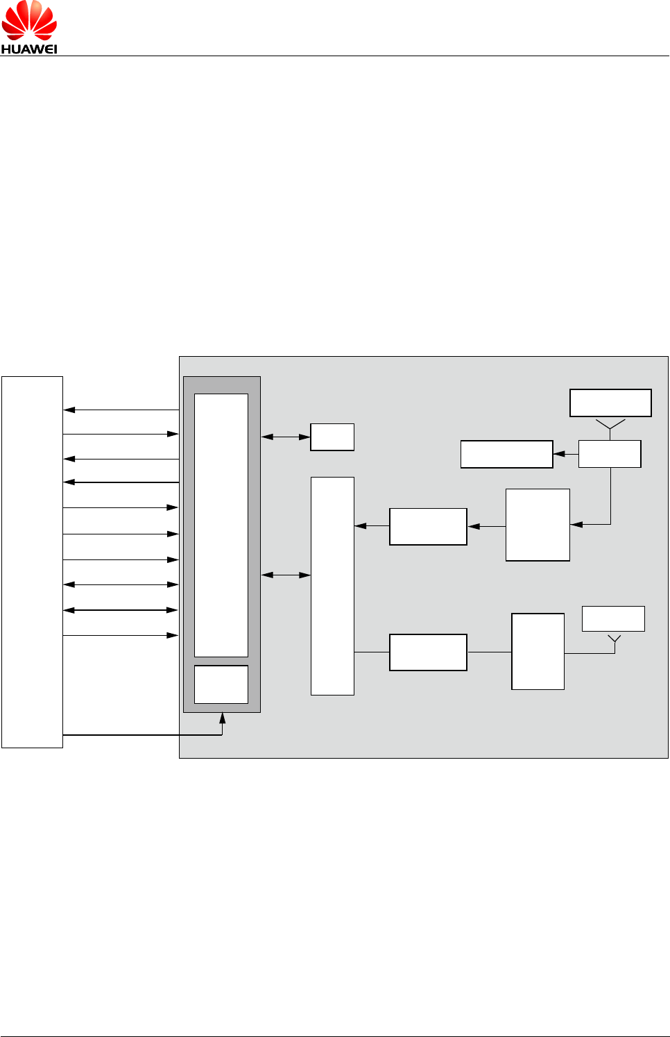
2.3 Circuit Block Diagram
Figure 2-1 shows the circuit block diagram of the MU736 module. The application
block diagram and major functional units of the MU736 module contain the following
parts:
- Baseband controller
- Power manager
- Multi-chip package (MCP) memory
- Radio frequency (RF) transceiver
- RF interface
- RF PA
Figure 2-1 Circuit block diagram of the MU736 module
BASE
BAND
RF TRANSCEIVER
Power
Manager
MCP
EBU
BodySAR_N
Wake_On_WWAN#
W_DISABLE#
LED#
GPS_DISABLE#
RESET#
Power_On_Off
Power
USIM
ANTCTL[0~3]
M.2
Interface
USB
GPS Front End Extractor
GPS/DIV ANT
RF Front End
Diversity
ANT
Switch
Main ANT
MAIN
ANT
Switch
RF Front End

HUAWEI MU736 HSPA+ M.2 Module
Hardware Guide
Description of the Application Interfaces
Issue 05 (2014-01-14)
Huawei Proprietary and Confidential
Copyright © Huawei Technologies Co., Ltd.
12
3 Description of the Application Interfaces
3.1 About This Chapter
This chapter mainly describes the external application interfaces of the MU736
module, including:
- 75-pin Gold Finger
- Power Interface
- Signal Control Interface
- USB Interface
- USIM Card Interface
- Tunable Antenna Control
- Config Pins
- NC Pins
- RF Antenna Interface
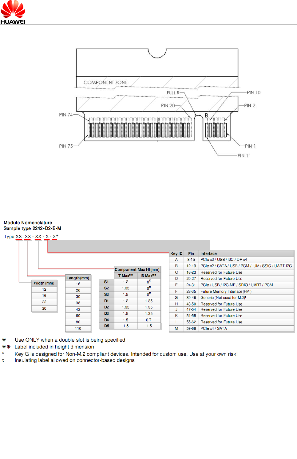
3.2 75-pin Gold Finger
The MU736 module uses a 75-pin Gold Finger as its external interface. For details
about the module and dimensions, see "6.2 Dimensions of MU736".
Figure 3-1 shows the sequence of pins on the 75-pin signal interface of the MU736
module.
HUAWEI MU736 HSPA+ M.2 Module
Hardware Guide
Description of the Application Interfaces
Issue 05 (2014-01-14)
Huawei Proprietary and Confidential
Copyright © Huawei Technologies Co., Ltd.
13
Figure 3-1 TOP view of sequence of Gold Finger interface pins
Table 3-1 shows the definitions of pins on the 75-pin signal interface (67 for signals
and 8 for notch) of the MU736 module.
As the M.2 naming nomenclature, MU736 is Type 3042-S3-B (30 mm × 42 mm,
Component Max Height on top is 1.5 mm and single-sided, Key ID is B.)
HUAWEI MU736 HSPA+ M.2 Module
Hardware Guide
Description of the Application Interfaces
Issue 05 (2014-01-14)
Huawei Proprietary and Confidential
Copyright © Huawei Technologies Co., Ltd.
14
Table 3-1 Definitions of pins on the M.2 interface
Pin
No.
Pin Name
I/O
Description
DC Characteristics (V)
Normal
Min.
Typ.
Max.
1
CONFIG_3
O
Connected to Ground internally.
MU736 is configured as WWAN-SSIC 0.
-
0
-
2
3.3V
PI
Power supply
3.135
3.3
4.4
3
Ground
PI
Ground
-
0
-
4
3.3V
PI
Power supply
3.135
3.3
4.4
5
Ground
PI
Ground
-
0
-
6
Power_On_Off
I
A single control to turn On/Off WWAN.
H: WWAN is powered on.
L: WWAN is powered off.
It is internally pulled to low.
It is 3.3 V tolerant but can be driven by
either 1.8 V or 3.3 V GPIO.
–0.3
1.8
3.6
7
USB_D+
IO
USB Data + defined in the USB 2.0
Specification
-
-
-
8
W_DISABLE#
I
WWAN disable function
H: WWAN function is determined by
software AT command. Default enabled.
L: WWAN function is turned off.
–0.3
3.3
3.6
9
USB_D-
IO
USB Data - defined in the USB 2.0
Specification
-
-
-
10
LED#
O
It is an open drain, active low signal,
used to allow the M.2 card to provide
status indicators via LED devices that
will be provided by the system.
Open drain and a pull-up
resistor is required on
the host
11
Ground
PI
Ground
-
0
-
12
Notch
-
-
-
-
-
13
Notch
-
-
-
-
-
14
Notch
-
-
-
-
-
15
Notch
-
-
-
-
-
16
Notch
-
-
-
-
-
17
Notch
-
-
-
-
-
18
Notch
-
-
-
-
-
19
Notch
-
-
-
-
-
HUAWEI MU736 HSPA+ M.2 Module
Hardware Guide
Description of the Application Interfaces
Issue 05 (2014-01-14)
Huawei Proprietary and Confidential
Copyright © Huawei Technologies Co., Ltd.
15
Pin
No.
Pin Name
I/O
Description
DC Characteristics (V)
Normal
Min.
Typ.
Max.
20
Reserved
-
Reserved for Future Use, please keep it
NC in host side.
-
-
-
21
CONFIG_0
O
Not Connected internally.
MU736 is configured as WWAN-SSIC 0.
-
-
-
22
Reserved
-
Reserved for Future Use, please keep it
NC in host side.
-
-
-
23
Wake_On_WWA
N#
O
WWAN to wake up the host.
It is open drain and active low.
Open drain and a pull-up
resistor is required on
the host
24
Reserved
-
Reserved for Future Use, please keep it
NC in host side.
-
-
-
25
BodySAR_N
I
Hardware pin for BodySAR Detection,
active low.
H: No TX power backoff (default).
L: TX power backoff.
–0.3
1.8
3.6
26
GPS_DISABLE#
I
GPS disable function
H: GPS function is determined by
software AT command. Default enabled.
L: GPS is turned off.
–0.3
3.3
3.6
27
Ground
PI
Ground
-
0
-
28
NC
-
Not Connected
-
-
-
29
NC
-
Not Connected
-
-
-
30
UIM_RESET
O
USIM Reset
–0.3
1.8/2.85
1.98
/3.0
31
NC
-
Not Connected
-
-
-
32
UIM_CLK
O
USIM Clock
–0.3
1.8/2.85
1.98
/3.0
33
Ground
PI
Ground
-
0
-
34
UIM_DATA
IO
USIM DATA
–0.3
1.8/2.85
1.98
/3.0
35
NC
-
Not Connected
-
-
-
36
UIM_PWR
PO
USIM POWER
–0.3
1.8/2.85
1.98
/3.3
37
NC
-
Not Connected
-
-
-
HUAWEI MU736 HSPA+ M.2 Module
Hardware Guide
Description of the Application Interfaces
Issue 05 (2014-01-14)
Huawei Proprietary and Confidential
Copyright © Huawei Technologies Co., Ltd.
16
Pin
No.
Pin Name
I/O
Description
DC Characteristics (V)
Normal
Min.
Typ.
Max.
38
NC
-
Not Connected
-
-
-
39
Ground
PI
Ground
-
0
-
40
I2C_SCL
IO
I2C clock
This function is under development.
–0.3
1.8
2.1
41
NC
-
Not Connected
-
-
-
42
I2C_SDA
IO
I2C data
This function is under development.
–0.3
1.8
2.1
43
NC
-
Not Connected
-
-
-
44
I2C_IRQ
I
Interrupt signal to wake up the module.
This function is under development.
–0.3
1.8
2.1
45
Ground
PI
Ground
-
0
-
46
SYSCLK
O
System clock output for external GNSS
module. MU736 does not support
GLONASS.
This function is under development.
–0.3
1.8
2.1
47
NC
-
Not Connected
-
-
-
48
TX_BLANKING
-
Tx blanking signal for external GNSS
module. MU736 doesn’t support
GLONASS.
This function is under development.
–0.3
1.8
2.1
49
NC
-
Not Connected
-
-
-
50
NC
-
Not Connected
-
-
-
51
Ground
PI
Ground
-
0
-
52
NC
-
Not Connected
-
-
-
53
NC
-
Not Connected
-
-
-
54
NC
-
Not Connected
-
-
-
55
NC
-
Not Connected
-
-
-
56
NC
-
Not Connected
-
-
-
57
Ground
PI
Ground
-
0
-
58
NC
-
Not Connected
-
-
-
59
ANTCTL0
O
Tunable antenna control signal, bit 0.
It is a push-pull type GPIO.
–0.3
1.8
2.1
HUAWEI MU736 HSPA+ M.2 Module
Hardware Guide
Description of the Application Interfaces
Issue 05 (2014-01-14)
Huawei Proprietary and Confidential
Copyright © Huawei Technologies Co., Ltd.
17
Pin
No.
Pin Name
I/O
Description
DC Characteristics (V)
Normal
Min.
Typ.
Max.
60
Reserved
-
Reserved for Future Use, please keep it
NC in host side.
-
-
-
61
ANTCTL1
O
Tunable antenna control signal, bit 1.
It is a push-pull type GPIO.
–0.3
1.8
2.1
62
Reserved
-
Reserved for Future Use, please keep it
NC in host side.
-
-
-
63
ANTCTL2
O
Tunable antenna control signal, bit 2.
It is a push-pull type GPIO.
–0.3
1.8
2.1
64
Reserved
-
Reserved for Future Use, please keep it
NC in host side.
-
-
-
65
ANTCTL3
O
Tunable antenna control signal, bit 3.
It is a push-pull type GPIO.
–0.3
1.8
2.1
66
SIM_DET
I
SIM hot swap detection pin.
Rising edge for insertion; falling edge for
removal.
H: SIM is present.
L: SIM is absent.
–0.3
1.8
2.1
67
RESET#
I
System reset, active low.
–0.3
1.8
3.6
68
NC
-
Not Connected
-
-
-
69
CONFIG_1
O
Connected to Ground internally.
MU736 is configured as WWAN-SSIC 0.
-
0
-
70
3.3V
PI
Power supply
3.135
3.3
4.4
71
Ground
PI
Ground
-
0
-
72
3.3V
PI
Power supply
3.135
3.3
4.4
73
Ground
PI
Ground
-
0
-
74
3.3V
PI
Power supply
3.135
3.3
4.4
75
CONFIG_2
O
Connected to Ground internally.
MU736 is configured as WWAN-SSIC 0.
-
0
-
P indicates power pins; I indicates pins for digital signal input; O indicates pins for digital signal
output.
HUAWEI MU736 HSPA+ M.2 Module
Hardware Guide
Description of the Application Interfaces
Issue 05 (2014-01-14)
Huawei Proprietary and Confidential
Copyright © Huawei Technologies Co., Ltd.
18
3.3 Power Interface
3.3.1 Overview
The power supply part of the MU736 module contains:
- 3.3V pins for the power supply
- UIM_PWR pin for USIM card power output
Table 3-2 lists the definitions of the pins on the power supply interface.
Table 3-2 Definitions of the pins on the power supply interface
Pin No.
Signal
Name
I/O
Description
DC Characteristics (V)
Min.
Typ.
Max.
2, 4, 70, 72, 74
3.3V
PI
Power supply for MU736,
3.3 V is recommended
3.135
3.3
4.4
36
UIM_PWR
PO
Power supply for USIM card
–0.3
1.8/2.85
1.98/3.3
3, 5, 11, 27, 33,
39, 45, 51, 57,
71, 73
Ground
PI
Ground
-
0
-
3.3.2 Power Supply 3.3V Interface
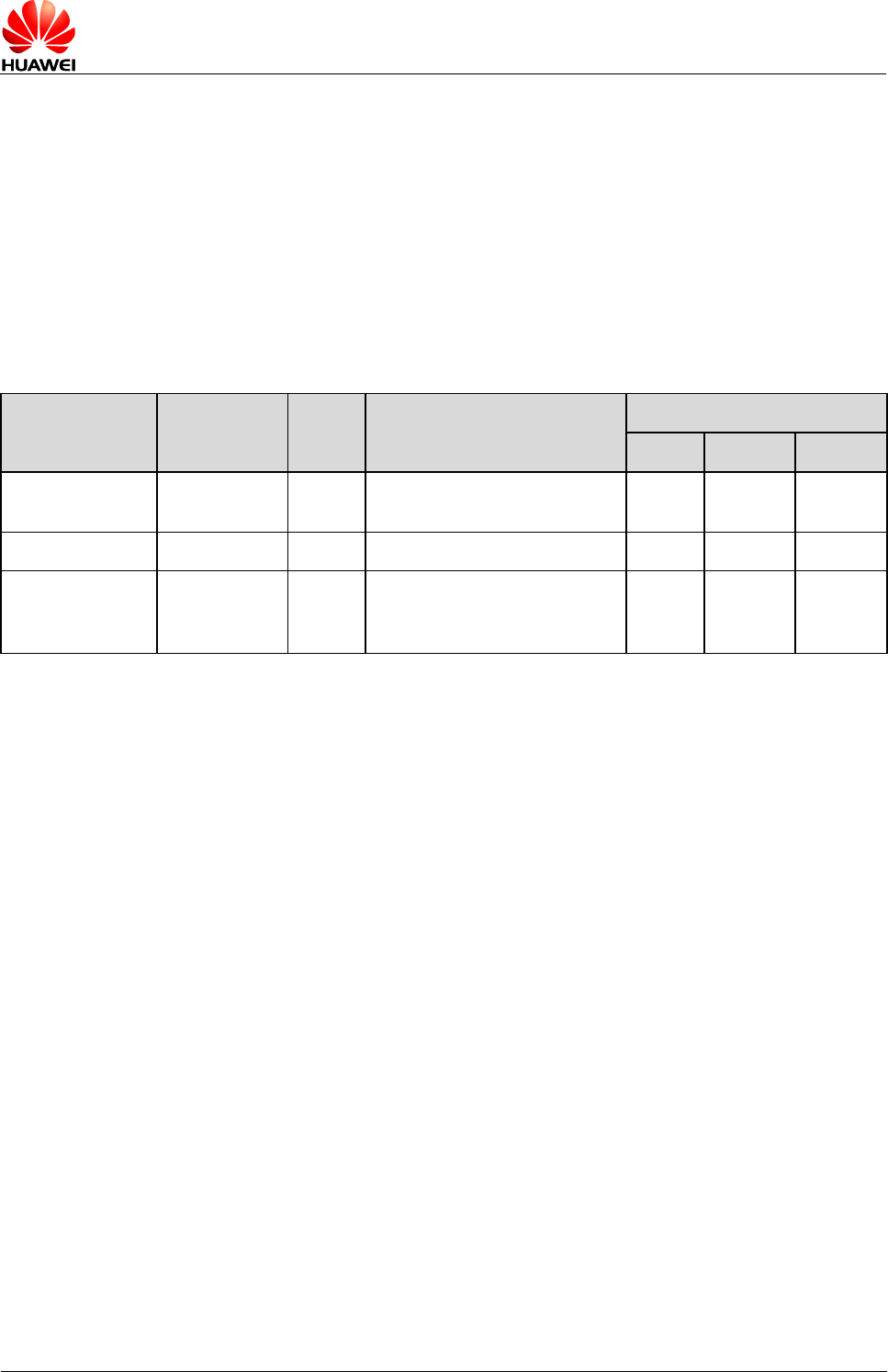
When the MU736 module works normally, power is supplied through the 3.3V pins
and the voltage ranges from 3.135 V to 4.4 V (typical value is 3.3 V). The MU736
provides 5 power pins, and 11 Ground pins. To ensure that the MU736 module works
normally, all the pins must be connected. The M.2 connector pin is defined to support
500 mA/Pin continuously.
When the MU736 module works at 2G mode, the module transmits at the maximum
power, the transient peak current may reach 2.5 A. In this case, the power pin voltage
will drop. Make sure that the voltage does not drop below 3.135 V in any case. The
traces of the power supply should be as short and wide as possible. It is
recommended that at least a 220 µF capacitance is added onto the 3.3 V power rails
and as close to the M.2 connector as possible. Customer can reduce the capacitance
if it can be guaranteed that 3.3V pin does not drop below 3.135 V in any case.
Figure 3-2 shows the recommended power circuit of the MU736 module.
HUAWEI MU736 HSPA+ M.2 Module
Hardware Guide
Description of the Application Interfaces
Issue 05 (2014-01-14)
Huawei Proprietary and Confidential
Copyright © Huawei Technologies Co., Ltd.
19
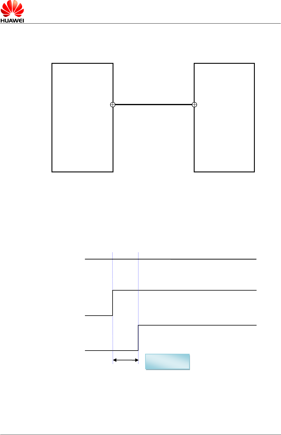
Figure 3-2 Recommended power circuit of the MU736 module
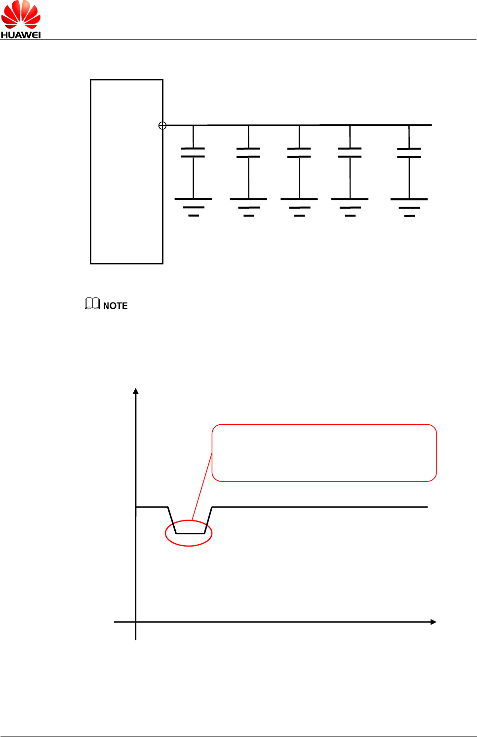
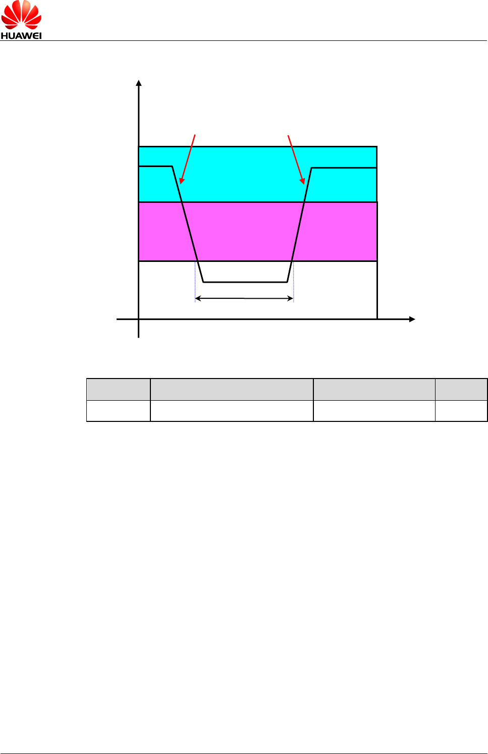
3.3V pin must never be under 3.135 V during the 2G transmitting burst, as shown in Figure 3-3 .
Figure 3-3 VCC drop during 2G transmitting
If customer wants to power cycle MU736, the 3.3V pin must stay below 1.8 V for more
than 100 ms. The sequence is shown as in Figure 3-4 .
3.135 V
3.3 V
4.4 V
Do not drop below 3.135 V, during 2G TX.
The maximum current may be 2.5 A.
Voltage
Time
MU736
3.3V
330pF
100nF
1µF
22µF
220µF
3.3V
HUAWEI MU736 HSPA+ M.2 Module
Hardware Guide
Description of the Application Interfaces
Issue 05 (2014-01-14)
Huawei Proprietary and Confidential
Copyright © Huawei Technologies Co., Ltd.
20
Figure 3-4 MU736 power supply time sequence for power cycling
Parameter
Remarks
Time(Min.)
Unit
Toff
Power off time
100
ms
3.3.3 USIM Power Output UIM_PWR
Output power supply interface is UIM_PWR. Through the UIM_PWR power supply
interface, the MU736 module can supply 1.8 V or 2.85 V power to UIM card. The max
current can reach 200 mA, so special attention on PCB design should be taken at the
host side.
3.4 Signal Control Interface
3.4.1 Overview
The signal control part of the interface in the MU736 module consists of the following:
- Power On/Off (Power_On_Off) pin
- System reset (RESET#) pin
- LED control (LED#) pin
- WWAN disable control (W_DISABLE#) pin
- GPS disable control (GPS_DISABLE#) pin
- Wake signal out from module (Wake_On_WWAN#) pin
1.8 V
3.135 V
4.4 V
Power Off
Voltage
Time
Power On
Undefined State
Power Off
Power On
Toff > 100 ms
HUAWEI MU736 HSPA+ M.2 Module
Hardware Guide
Description of the Application Interfaces
Issue 05 (2014-01-14)
Huawei Proprietary and Confidential
Copyright © Huawei Technologies Co., Ltd.
21
- BodySAR detection (BodySAR_N) pin
- UIM detection (SIM_DET) pin
Table 3-3 lists the pins on the signal control interface.
Table 3-3 Pins on the signal control interface
Pin
No.
Pin Name
I/O
Description
DC Characteristics(V)
Min.
Typ.
Max.
6
Power_On_Off
I
A single control to turn On/Off
WWAN. When It is High, WWAN is
powered on.
H: Power on
L: Power off
It is internally pulled to low.
It is 3.3 V tolerant but can be driven
by either 1.8 V or 3.3 V GPIO.
–0.3
1.8
3.6
67
RESET#
I
System reset, active low
–0.3
1.8
3.6
10
LED#
O
It is an open drain, active low signal,
used to allow the M.2 card to provide
status indicators via LED devices that
will be provided by the system.
Open drain and a pull-up
resistor is required on the
host
8
W_DISABLE#
I
WWAN disable function
H: WWAN function is determined by
software AT command. Default
enabled.
L: WWAN function is turned off.
–0.3
3.3
3.6
26
GPS_DISABLE#
I
GPS disable function
H: GPS function is determined by
software AT command. Default
enabled.
L: GPS is turned off.
–0.3
3.3
3.6
23
Wake_On_WWAN#
O
It is open drain, WWAN to wake up
the host, active low.
Open drain and a pull-up
resistor is required on the
host
25
BodySAR_N
I
Hardware pin for BodySAR detection.
H: No TX power backoff (default).
L: TX power backoff.
–0.3
1.8
3.6
66
SIM_DET
I
SIM hot swap detection pin.
Rising edge for insertion; falling edge
for removal.
H: SIM is present.
L: SIM is absent.
–0.3
1.8
2.1
HUAWEI MU736 HSPA+ M.2 Module
Hardware Guide
Description of the Application Interfaces
Issue 05 (2014-01-14)
Huawei Proprietary and Confidential
Copyright © Huawei Technologies Co., Ltd.
22
3.4.2 Power_On_Off Control Pin
The MU736 module can be controlled to be powered on/off by the Power_On_Off pin.
Table 3-4 Two states of Power_On_Off
Item.
Pin state
Description
1
High
MU736 is powered on.
NOTE: If MU736 needs to be powered on automatically, the
Power_On_Off pin must be pulled up to 3.3 V.
2
Low
MU736 is powered off.
It is internally pulled to low.
MU736 is powered by regulated 3.3 V
If MU736 is powered by 3.3 V voltage regulator (such as notebook or Ultrabook),
Power_On_Off pin should be pulled up to 3.3 V through a resistor.
The pull-up resistor should be not larger than 10 kΩ.
The following are the power On/Off sequences:
1. The module gets 3.3 V when power supply for the module is switched on.
2. The module is turned on since Power_On_Off pin is pulled up directly to 3.3 V.
3. Host cuts off 3.3V supply to power off the module.
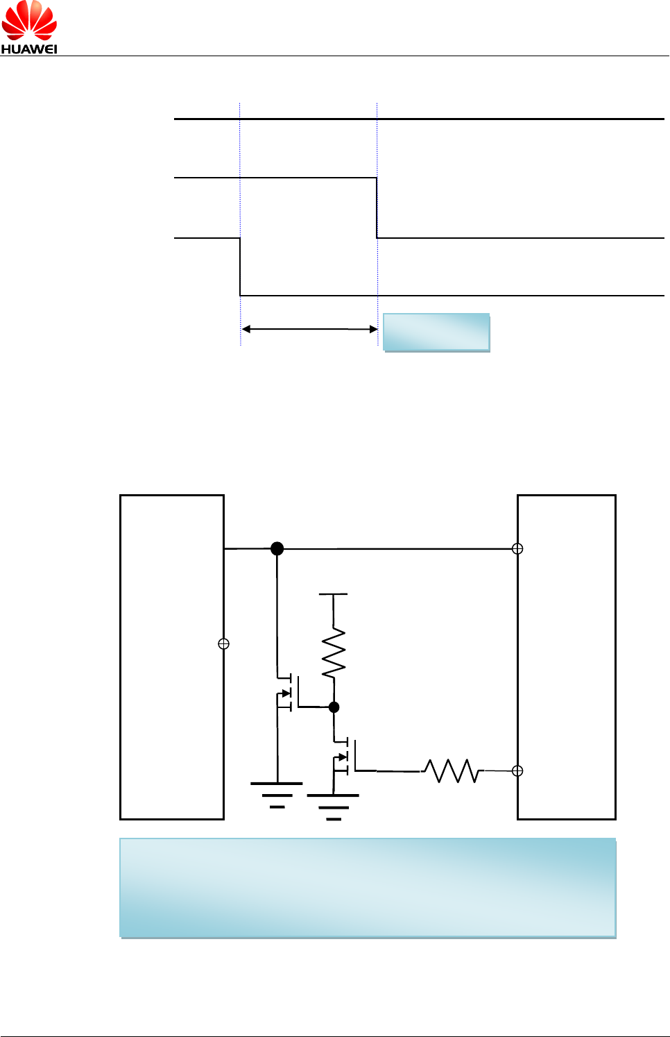
The recommended circuit is shown as in Figure 3-5 .
Figure 3-5 Recommended connections of Power_On_Off pins (Auto power)
Power on sequence
Do not toggle RESET# pin during the power on sequence. Pulling RESET# pin low
will extend time for module startup.
Recommended power on timing is shown as in Figure 3-6 .
MU736
Pin 2, 4, 70, 72, 74
Pin 6
10 kΩ
Power_On_Off
3.3V
HUAWEI MU736 HSPA+ M.2 Module
Hardware Guide
Description of the Application Interfaces
Issue 05 (2014-01-14)
Huawei Proprietary and Confidential
Copyright © Huawei Technologies Co., Ltd.
23
Figure 3-6 Recommended power on off timing
Power off Sequence
Cutting off 3.3V will power off the module.
Figure 3-7 Recommended power off timing (cut off 3.3V)
MU736 is powered directly to battery
For use case MU736 is connected directly to battery, such as tablet platforms,
Power_On_Off pin should be controlled by a GPIO from host to control MU736 power
On/Off.
It is critical to make sure the module is safely powered off when the Tablet SoC is shut
off. There will be current leakage if the module is not powered off properly. So It is
important to keep Power_On_Off pin logic low for more than 500 ms to power off the
module.
3.3V
RESET#
Power_On_Off
Power off
3.3V
RESET#
Power on
Power_On_Off
HUAWEI MU736 HSPA+ M.2 Module
Hardware Guide
Description of the Application Interfaces
Issue 05 (2014-01-14)
Huawei Proprietary and Confidential
Copyright © Huawei Technologies Co., Ltd.
24
The recommended connections are shown as in Figure 3-8 .
Figure 3-8 Recommended connections of Power_On_Off pins (Control)
Power on sequence
Do not toggle RESET# pin during power on sequence. Pulling RESET# pin low will
extend time for module startup.
Recommended power on timing is shown as in Figure 3-9 .
Figure 3-9 Recommended power on timing
Power off Sequence
Keep Power_On_Off pin logic low for more than 500 ms to power off the module.
3.3V (Vbatt,
always on)
RESET#
Power_On_off
Power on
t0 ≥ 0 ms
t0
MU736
Pin 6
HOST
GPIO
Power_On_Off
HUAWEI MU736 HSPA+ M.2 Module
Hardware Guide
Description of the Application Interfaces
Issue 05 (2014-01-14)
Huawei Proprietary and Confidential
Copyright © Huawei Technologies Co., Ltd.
25
Figure 3-10 Recommended power off timing (connect to battery)
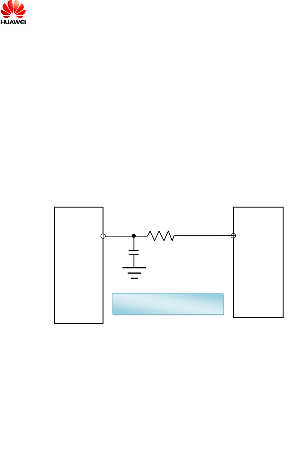
If there is limitation on the controlling GPIO to be programmable 500 ms, the hardware
solution can be used, as shown in Figure 3-11 .
Figure 3-11 Power on off circuit (hardware solution)
MU736
Pin 6
HOST
0 Ω
VCCGPIO2
1MΩ
NMOS
NMOS
3.3V (battery)
GPIO2
Q1
Q2
Power_On_Off
VCCGPIO2 is the power domain of the GPIO2.
When VCCGPIO2 is ON, Q2 is on and Q1 is off. So the Pin6 is controlled by
GPIO2 of host.
When VCCGPIO2 is Off, Q2 is off and Q1 is on. So the Pin6 is pulled low,
then the module is powered off.
Power off
t1 ≥ 500 ms
t1
Logic low or high-impedance (preferred)
Logic low or high-impedance (preferred)
Power_On_Off
RESET#
3.3V (Vbatt,
always on)
HUAWEI MU736 HSPA+ M.2 Module
Hardware Guide
Description of the Application Interfaces
Issue 05 (2014-01-14)
Huawei Proprietary and Confidential
Copyright © Huawei Technologies Co., Ltd.
26
3.4.3 RESET# Pins
The MU736 module can be reset through the RESET# pin asynchronous, active low.
Whenever this pin is active, the module will immediately be placed in a Power On
reset condition. Care should be taken for this pin unless there is a critical failure and
all other methods of regaining control and/or communication with the WWAN
sub-system have failed.
Pulling RESET# pin low for more than 20 ms will reset the module.
RESET# pin is optional, which cannot be connected. Pulling Power_On_Off pin low
for more than 500 ms can work as a reset.
RESET# pin is internally pulled up to 1.8 V, which is automatically on when 3.3 V is
applied even though Power_On_Off pin is low. Cautions should be taken on circuit
design otherwise there may be back driving issue.
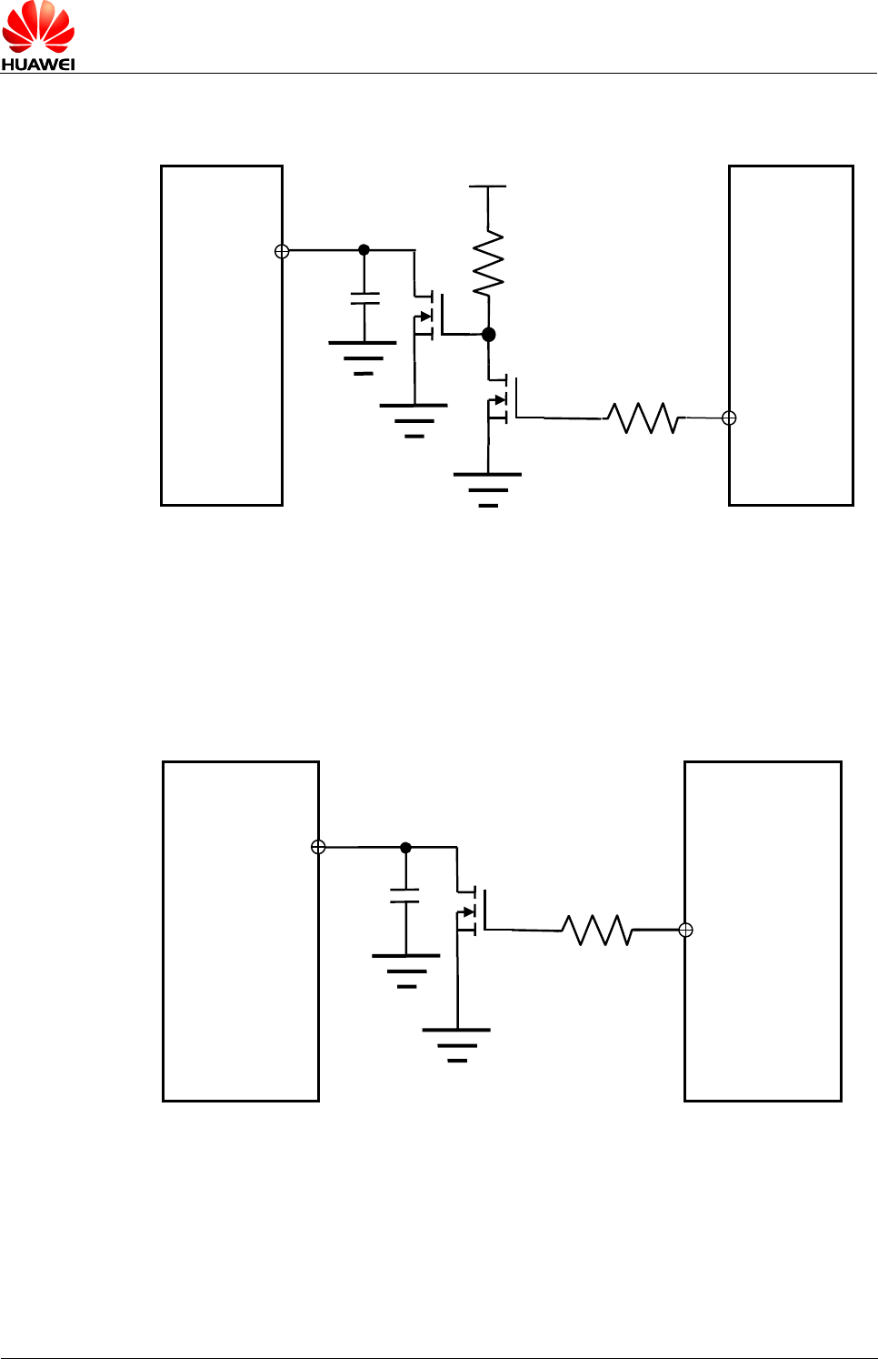
Option 1: Hardware circuit for RESET#
In this case, the GPIO is high-impedance when the module is powered off.
Figure 3-12 Hardware circuit for RESET# (Option 1)
Option 2: Hardware circuit for RESET#
In this case, the GPIO is not high-impedance when It is powered off.
Use 2 NMOSFET so that the logic of RESET# pin and GPIO are the same.
MU736
Pin 67
0 Ω
RESET#
HOST
GPIO1
GPIO1 should be high-impedance
when it is powered off.
33 рF
HUAWEI MU736 HSPA+ M.2 Module
Hardware Guide
Description of the Application Interfaces
Issue 05 (2014-01-14)
Huawei Proprietary and Confidential
Copyright © Huawei Technologies Co., Ltd.
27
Figure 3-13 Hardware circuit for RESET# (Option 2)
Option 3: Hardware circuit for RESET#
In this case, the GPIO is not high-impedance when the host is powered off.
Use only one NMOSFET, in this case the logic of RESET# pin and GPIO1 is reversed.
Figure 3-14 Hardware circuit for RESET# (Option 3)
HOST
MU736
0 Ω
RESET#
Pin 67
GPIO1
33 рF
MU736
RESET#
Pin 67
HOST
0 Ω
GPIO1
1MΩ
NMOS
NMOS
VCCGPIO1
33 рF
HUAWEI MU736 HSPA+ M.2 Module
Hardware Guide
Description of the Application Interfaces
Issue 05 (2014-01-14)
Huawei Proprietary and Confidential
Copyright © Huawei Technologies Co., Ltd.
28
- As the RESET# pin signal is relatively sensitive, it is recommended to install a 33
pF capacitor near to the M.2 pin.
- Triggering the RESET# pin signal will lead to loss of all data in the module
and the removal of system drivers. It will also disconnect the module from
the network resulting in a call drop.
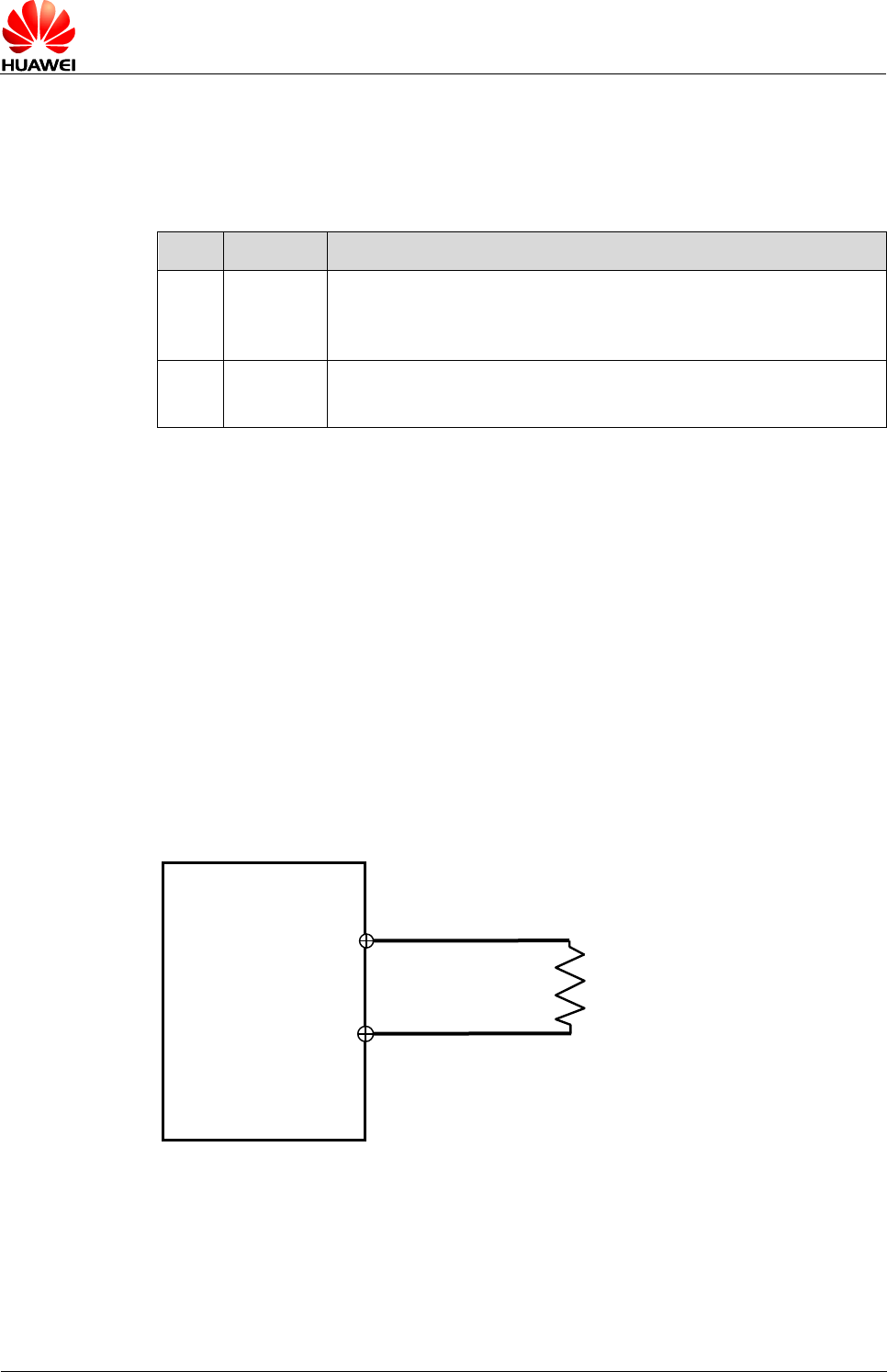
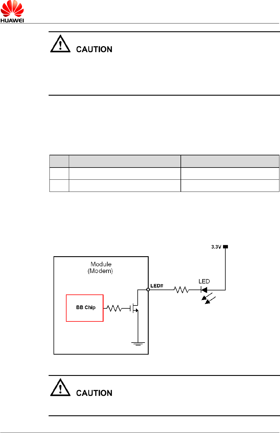
3.4.4 LED# Pin
MU736 provides an open drain signal to indicate the RF status.
Table 3-5 State of the LED# pin
No.
Operating Status
LED#
1
RF function is turned on
Outputs Low
2
RF function is turned off
Outputs High
Figure 3-15 shows the recommended circuits of the LED# pin. The brightness of LED
can be adjusted by adjusting the resistance of the series resistor.
Figure 3-15 Driving circuit
LED# pin output is different from HUAWEI MU733 module, because MU736
integrates a MOSFET inside.
HUAWEI MU736 HSPA+ M.2 Module
Hardware Guide
Description of the Application Interfaces
Issue 05 (2014-01-14)
Huawei Proprietary and Confidential
Copyright © Huawei Technologies Co., Ltd.
29
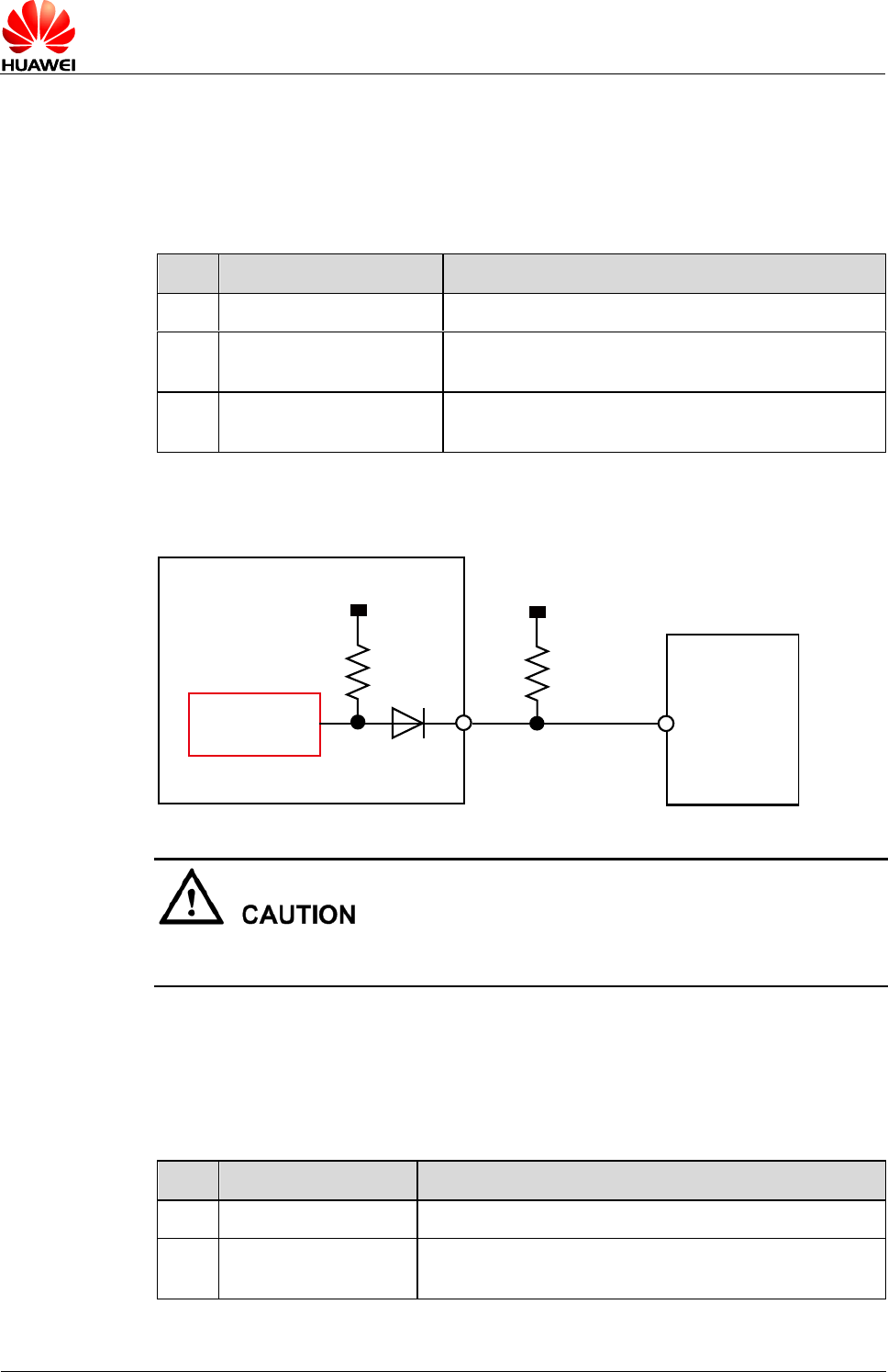
3.4.5 W_DISABLE# Pin
MU736 provides a hardware pin (W_DISABLE#) to enable/disable the radio function.
This function also can be implemented by AT command.
Table 3-6 Function of the W_DISABLE# pin
No.
W_DISABLE#
Function
1
Low
WWAN function will be turned off.
2
High
WWAN function is determined by software AT
command. Default enabled.
3
Floating
WWAN function is determined by software AT
command. Default enabled.
Figure 3-16 Connections of the W_DISABLE# pin
Module
(Modem)
BB Chip
1.8V
W_DISABLE#
VCC From Host
10 kΩ
Host
It is recommended not to add a diode on the W_DISABLE# pin outside the MU736
module.
3.4.6 GPS_DISABLE# Pin
MU736 provides a hardware pin (GPS_DISABLE#) to enable/disable the GPS
function.
Table 3-7 Function of the GPS_DISABLE# pin
No.
GPS_DISABLE#
Function
1
Low
GPS function is disabled.
2
High
GPS function is determined by software AT
command. Default enabled.
HUAWEI MU736 HSPA+ M.2 Module
Hardware Guide
Description of the Application Interfaces
Issue 05 (2014-01-14)
Huawei Proprietary and Confidential
Copyright © Huawei Technologies Co., Ltd.
30
No.
GPS_DISABLE#
Function
3
Floating
GPS function is determined by software AT
command. Default enabled.
Figure 3-17 Connections of the GPS_DISABLE# pin
Module
(Modem)
BB Chip
1.8V
GPS_DISABLE#
VCC From Host
10 kΩ
Host
It is recommended not to add a diode on the GPS_DISABLE# pin outside the MU736
module.
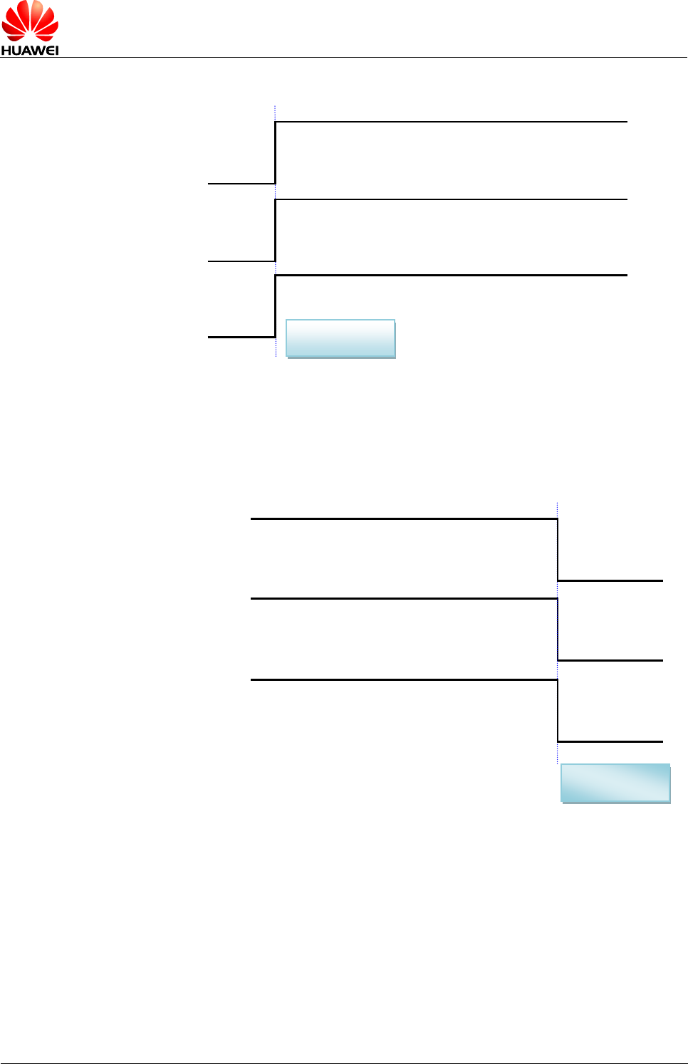
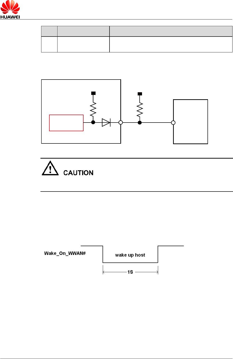
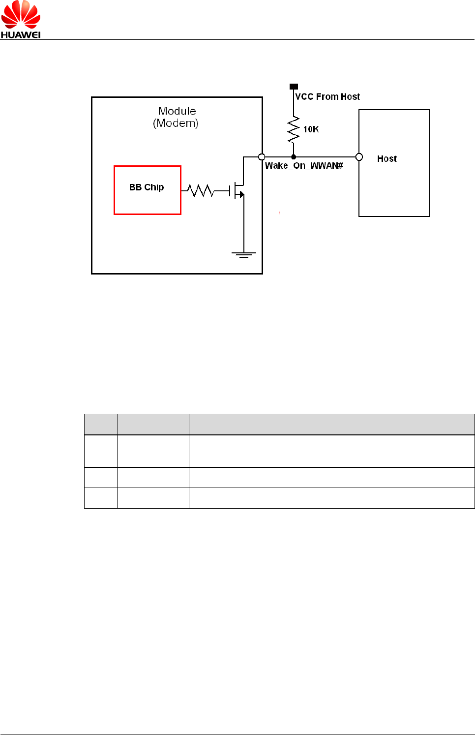
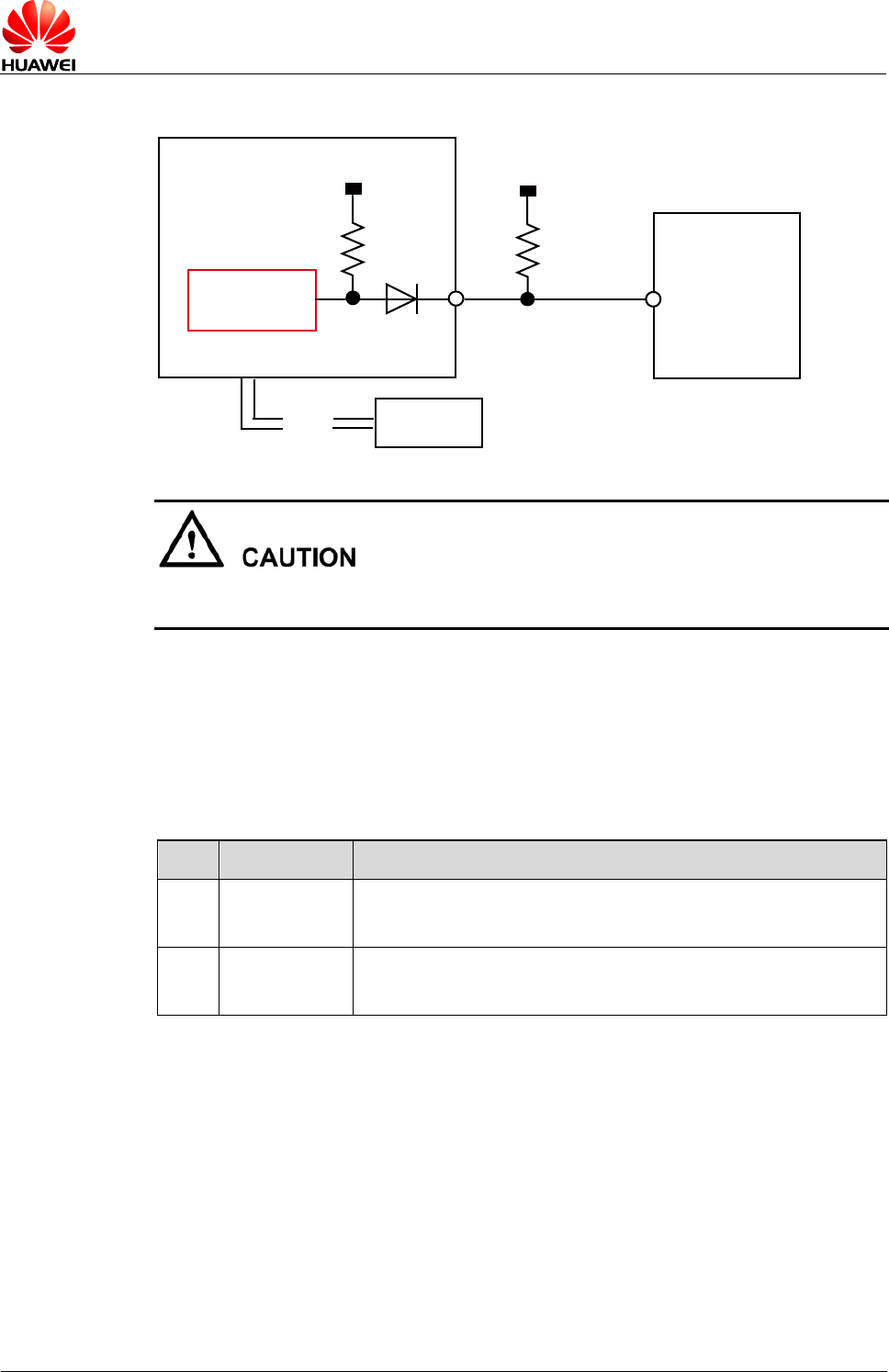
3.4.7 Wake_On_WWAN# Pin
MU736 provides an open drain output Wake_On_WWAN# pin to wake host. It is low
active.
Figure 3-18 Wave form of the Wake_On_WWAN# pin
HUAWEI MU736 HSPA+ M.2 Module
Hardware Guide
Description of the Application Interfaces
Issue 05 (2014-01-14)
Huawei Proprietary and Confidential
Copyright © Huawei Technologies Co., Ltd.
31
Figure 3-19 Connections of the Wake_On_WWAN# pin
3.4.8 BodySAR_N Pin
MU736 provides an input pin BodySAR_N for BodySAR detection.
It is pulled up internally and when it is pulled low by the proximity sensor output or
controlling signal from host systems, the Tx power reduction actions will be triggered.
Table 3-8 Function of the BodySAR_N pin
No.
BodySAR_N
Function
1
Low
MAX TX power will be back off by setting through AT
command
2
High
MAX TX power will NOT be backed off (default)
3
Floating
MAX TX power will NOT be backed off
If BodySAR_N pin is used to monitor the proximity sensor output, there are some
essential preconditions for this hardware solution.
MU736 cannot provide any control signal for the proximity sensor. Any control or
programming required by the proximity sensor should be handled by the host side.
HUAWEI MU736 HSPA+ M.2 Module
Hardware Guide
Description of the Application Interfaces
Issue 05 (2014-01-14)
Huawei Proprietary and Confidential
Copyright © Huawei Technologies Co., Ltd.
32
Figure 3-20 Connections of the BodySAR_N pin
Module
(Modem)
BB Chip
1.8V
BodySAR_N
VCC From Host
10 kΩ
Proximity
sensor
USB Host AP
It is recommended not to add a diode on the BodySAR_N pin outside the MU736
module.
3.4.9 SIM_DET Pin
MU736 supports USIM Hot Swap function.
MU736 provides an input pin (SIM_DET) to detect whether the USIM card is present
or not. This pin is an edge trigger pin.
Table 3-9 Function of the SIM_DET pin
No.
SIM_DET
Function
1
Rising edge
USIM Card insertion.
If the USIM Card is present, SIM_DET pin should be high.
2
Falling edge
USIM Card removal.
If the USIM Card is absent, SIM_DET pin should be low.
HUAWEI MU736 HSPA+ M.2 Module
Hardware Guide
Description of the Application Interfaces
Issue 05 (2014-01-14)
Huawei Proprietary and Confidential
Copyright © Huawei Technologies Co., Ltd.
33
Figure 3-21 Connections of the SIM_DET pin
CD is a pin detecting USIM in the SIM Socket, normally, there will be a detect pin in
the SIM Socket.
- The Normal SHORT SIM connector should be employed. The logic of SIM_DET
pin is shown as Figure 3-22 . High represents that SIM is inserted; Low represents
that SIM is removed.
- When SIM is inserted (hot), SIM_DET pin will change from Low to High;
- When SIM is removed (hot), SIM_DET pin will change from High to Low.
- MU736 will detect the rising or falling edge of SIM_DET to react the hot swap.
Figure 3-22 The logic of SIM_DET
Modem
Processor
SIM Connector Switch
SIM installed=
Not Connected
SIM not
installed=
GND
WWAN Module
SIM_DET
1.8V
HUAWEI MU736 HSPA+ M.2 Module
Hardware Guide
Description of the Application Interfaces
Issue 05 (2014-01-14)
Huawei Proprietary and Confidential
Copyright © Huawei Technologies Co., Ltd.
34
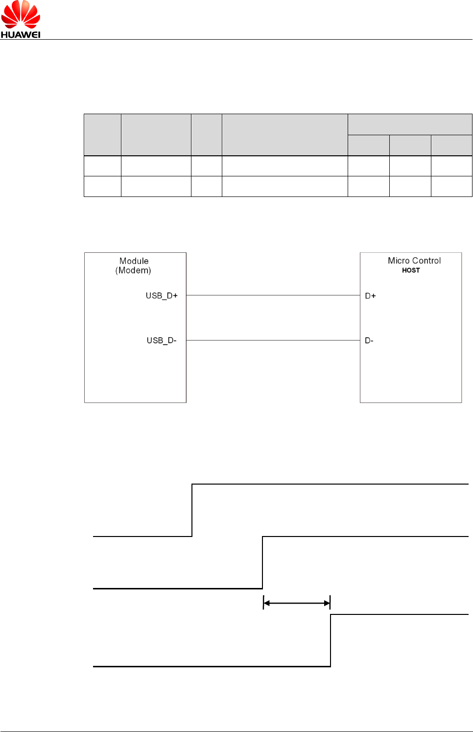
3.5 USB Interface
The MU736 is compliant with USB 2.0 high speed protocol. The USB input/output
lines are following USB 2.0 specifications. Definition of the USB interface:
Pin
No.
Pin Name
I/O
Description
DC Characteristics (V)
Min.
Typ.
Max.
7
USB_D+
I/O
USB data signal D+
-
-
-
9
USB_D-
I/O
USB data signal D-
-
-
-
Figure 3-23 Recommended circuit of USB interface
Figure 3-24 shows the timing sequence between 3.3 V and USB D+.
Figure 3-24 MU736 USB D+ and 3.3 V power on timing
3.3V
Power_On_Off
USB D+
Tpd
HUAWEI MU736 HSPA+ M.2 Module
Hardware Guide
Description of the Application Interfaces
Issue 05 (2014-01-14)
Huawei Proprietary and Confidential
Copyright © Huawei Technologies Co., Ltd.
35
Parameter
Remarks
Time(Nominal value)
Unit
Tpd
Power valid to USB D+ high
8
s
The layout design of this circuit on the host board should comply with the USB 2.0 high speed
protocol, with differential characteristic impedance of 90 Ω.
3.6 USIM Card Interface
3.6.1 Overview
The MU736 module provides a USIM card interface complying with the ISO 7816-3
standard and supports both 1.8 V and 3.0 V USIM cards.
Table 3-10 USIM card interface signals
Pin
No.
Pin Name
I/O
Description
DC Characteristics (V)
Min.
Typ.
Max.
30
UIM_RESET
O
USIM Reset
–0.3
1.8/2.85
1.98/3.0
32
UIM_CLK
O
USIM clock
–0.3
1.8/2.85
1.98/3.0
34
UIM_DATA
IO
USIM DATA
–0.3
1.8/2.85
1.98/3.0
36
UIM_PWR
PO
USIM POWER
–0.3
1.8/2.85
1.98/3.0
3.6.2 Circuit Recommended for the USIM Card Interface
As the MU736 module is not equipped with an USIM socket, you need to place an
USIM socket on the user interface board.
Figure 3-25 shows the circuit of the USIM card interface.
HUAWEI MU736 HSPA+ M.2 Module
Hardware Guide
Description of the Application Interfaces
Issue 05 (2014-01-14)
Huawei Proprietary and Confidential
Copyright © Huawei Technologies Co., Ltd.
36
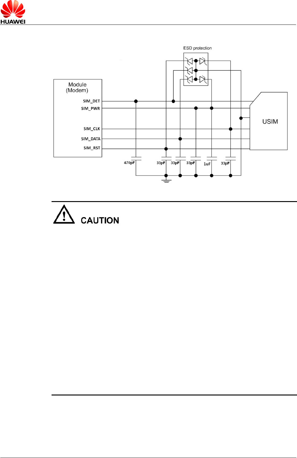
Figure 3-25 Circuit of the USIM card interface
- The ESD protection component should choose low capacitance. The capacitance
of the component should be less than 10 pF.
- To meet the requirements of 3GPP TS 51.010-1 protocols and electromagnetic
compatibility (EMC) authentication, the USIM socket should be placed near the
M.2 interface (it is recommended that the PCB circuit connects the M.2 interface
and the USIM socket does not exceed 100 mm), because a long circuit may lead to
wave distortion, thus affecting signal quality.
- It is recommended that you wrap the area adjacent to the SIM_CLK and
SIM_DATA signal wires with ground. The Ground pin of the USIM socket and the
Ground pin of the USIM card must be well connected to the power Ground pin
supplying power to the MU736 module.
- A 100 nF capacitor (0402 package is recommended so that larger capacitance
such as 1µF can be employed if necessary) and a 33 pF capacitor are placed
between the SIM_VCC and Ground pins in parallel. Three 33 pF capacitors are
placed between the SIM_DATA and Ground pins, the SIM_RST and Ground pins,
and the SIM_CLK and Ground pins in parallel to filter interference from RF signals.
- It is recommended to take electrostatic discharge (ESD) protection measures near
the USIM card socket. Transient voltage suppressor diode should be placed as
close as possible to the USIM socket, and the Ground pin of the ESD protection
component is well connected to the power Ground pin that supplies power to the
MU736 module.
3.7 Tunable Antenna Control
The module provides 4 tunable antenna control pins.
HUAWEI MU736 HSPA+ M.2 Module
Hardware Guide
Description of the Application Interfaces
Issue 05 (2014-01-14)
Huawei Proprietary and Confidential
Copyright © Huawei Technologies Co., Ltd.
37
Table 3-11 List of ANTCTL pins
Pin
No.
Pin Name
I/O
Description
DC Characteristics(V)
Min.
Typ.
Max.
59
ANTCTL0
O
Tunable antenna control signal bit 0.
It is a push-pull type GPIO.
–0.3
1.8
2.1
61
ANTCTL1
O
Tunable antenna control signal bit 1.
It is a push-pull type GPIO.
–0.3
1.8
2.1
63
ANTCTL2
O
Tunable antenna control signal bit 2.
It is a push-pull type GPIO.
–0.3
1.8
2.1
65
ANTCTL3
O
Tunable antenna control signal bit 3.
It is a push-pull type GPIO.
–0.3
1.8
2.1
3.8 Config Pins
The module provides 4 config pins. MU736 is configured as WWAN-SSIC 0.
Table 3-12 List of CONFIG pins
Pin
No.
Pin Name
I/O
Description
DC Characteristics(V)
Min.
Typ.
Max.
1
CONFIG_3
O
Connected to GND internally
-
0
-
21
CONFIG_0
O
Not Connected internally
-
-
-
69
CONFIG_1
O
Connected to GND internally
-
0
-
75
CONFIG_2
O
Connected to GND internally
-
0
-
In the M.2 specification, the 4 pins are defined as Table 3-13 .
Table 3-13 List of Config pins
Config_0
(Pin 21)
Config_1
(Pin 69)
Config_2
(Pin 75)
Config_3 (Pin
1)
Module type and
Main host interface
Port
Configuration
Ground
Ground
Ground
Ground
SSD-SATA
N/A
Ground
NC
Ground
Ground
SSD-PCIe
N/A
NC
Ground
Ground
Ground
WWAN-SSIC
0
NC
NC
NC
NC
No Module present
N/A
HUAWEI MU736 HSPA+ M.2 Module
Hardware Guide
Description of the Application Interfaces
Issue 05 (2014-01-14)
Huawei Proprietary and Confidential
Copyright © Huawei Technologies Co., Ltd.
38
The GPIO0~7 pins have configurable assignments. There are 4 possible functional
pin out configurations. These 4 configurations are called Port Config0~3. In each Port
Configuration each GPIO is defined as a specific functional pin. The GPIO pin
assignment can see in Table 3-14 . MU736 supports Config0. But the audio function is
not implemented in MU736.
Table 3-14 GPIO Pin Function Assignment per Port Configuration
GPIO Pin
Port Config0 (GNSS+Audio ver1)
GPIO_0 (Pin 40)
GNSS_SCL
GPIO_1 (Pin 42)
GNSS_SDA
GPIO_2 (Pin 44)
GNSS_I2C_IRQ
GPIO_3 (Pin 46)
SYSCLK
GPIO_4 (Pin 48)
TX_Blanking
GPIO_5 (Pin 20)
Audio_0 (not supported )
GPIO_6 (Pin 22)
Audio_1 (not supported)
GPIO_7 (Pin 24)
Audio_2 (not supported)
3.9 NC Pins
The module has some NC pins. All of NC pins are not connected in the module.
Table 3-15 List of NC pins
Pin No.
Pin Name
I/O
Description
DC Characteristics(V)
Min.
Typ.
Max.
28, 29, 31, 35, 37, 38,
41, 43, 47, 49, 50, 52,
53, 54, 55, 56, 58, 68
NC
-
Not Connected
-
-
-
3.10 RF Antenna Interface
3.10.1 RF Connector location
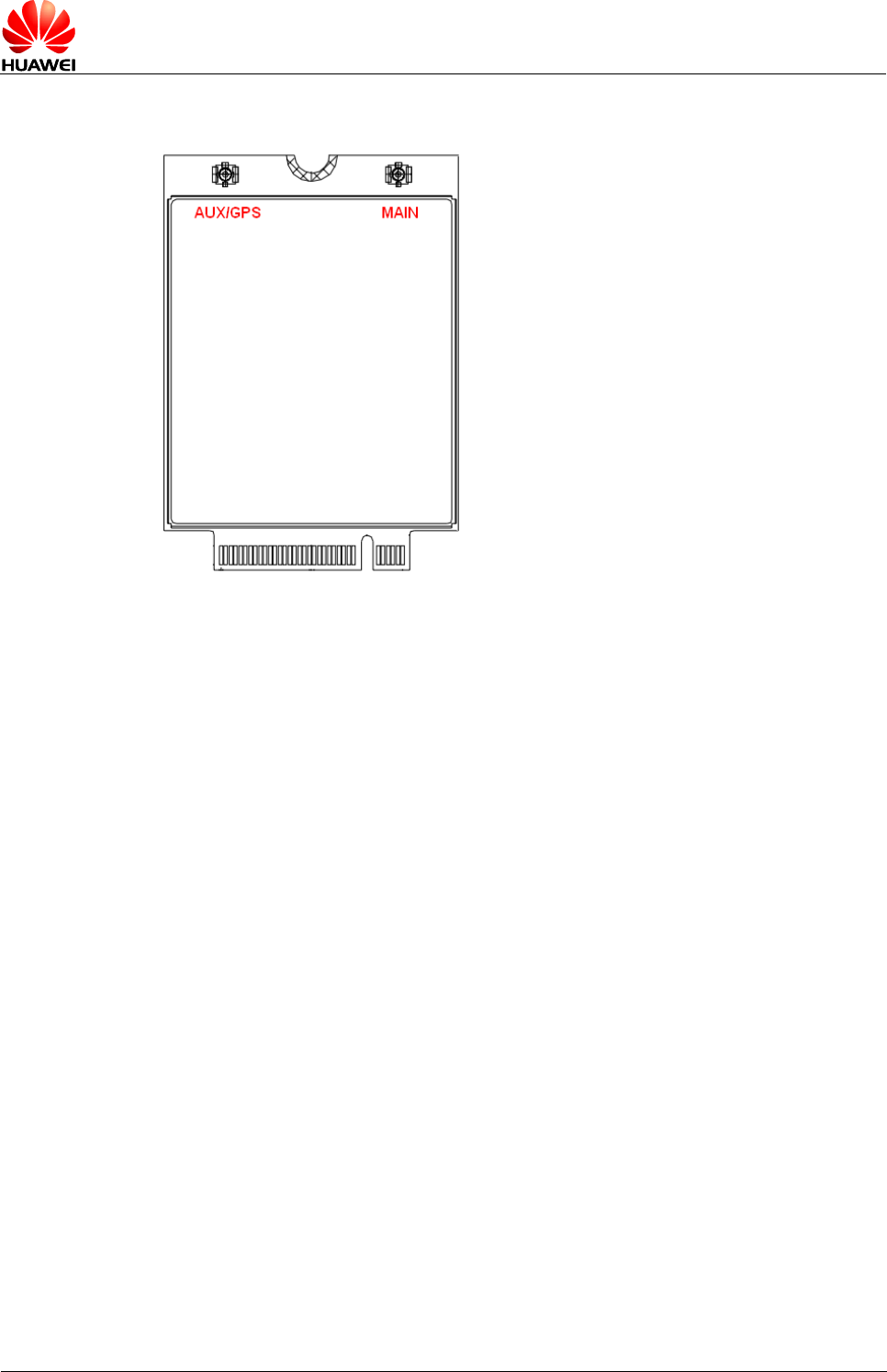
MU736 module provides 2 antenna connectors for connecting the external antennas.
HUAWEI MU736 HSPA+ M.2 Module
Hardware Guide
Description of the Application Interfaces
Issue 05 (2014-01-14)
Huawei Proprietary and Confidential
Copyright © Huawei Technologies Co., Ltd.
39
Figure 3-26 RF antenna connectors
3.10.2 Coaxial RF Connector Guidelines
- The antenna interface must be used with coaxial cables with characteristic
impedance of 50 Ω.
- The MU736 module supports the buckled RF connector antenna connection
methods: buckled RF connector MM4829-2702RA4 by MURATA or other
equivalent connectors
Figure 3-27 shows the RF connector dimensions.
HUAWEI MU736 HSPA+ M.2 Module
Hardware Guide
Description of the Application Interfaces
Issue 05 (2014-01-14)
Huawei Proprietary and Confidential
Copyright © Huawei Technologies Co., Ltd.
40
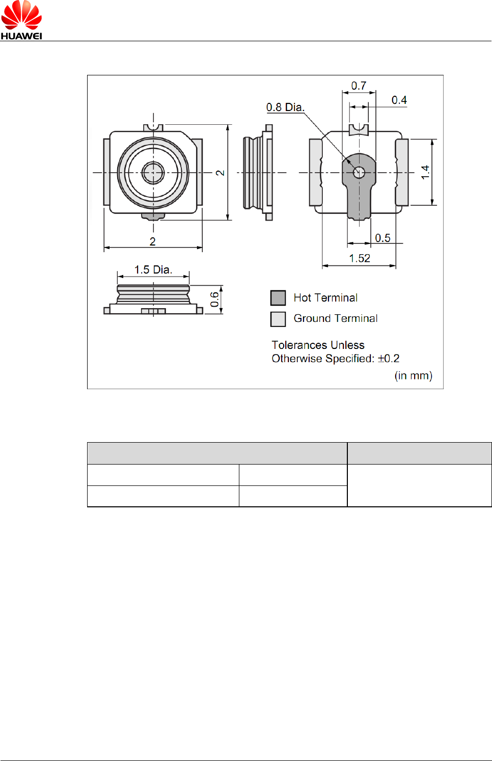
Figure 3-27 RF connector dimensions
Table 3-16 The major specifications of the RF connector
Rated Condition
Environmental Condition
Frequency range
DC to 6 GHz
Temperature range:
–40°C to +85°C
Characteristic impedance
50 Ω
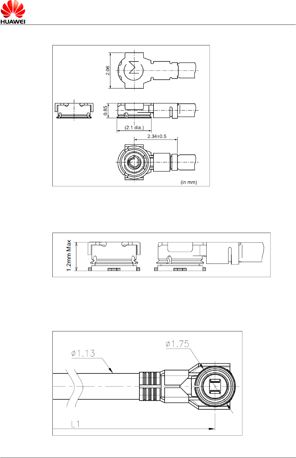
There are two kinds of coaxial cables mating the RF connector in the MU736.
Figure 3-28 shows the specifications of 0.81 mm coaxial cable mating the
recommended RF connector.
HUAWEI MU736 HSPA+ M.2 Module
Hardware Guide
Description of the Application Interfaces
Issue 05 (2014-01-14)
Huawei Proprietary and Confidential
Copyright © Huawei Technologies Co., Ltd.
41
Figure 3-28 Specifications of 0.81 mm coaxial cable mating with the RF connector
Figure 3-29 shows the connection between the RF connector and the 0.81 mm cable.
Figure 3-29 Connection between the RF connector and the 0.81 mm cable
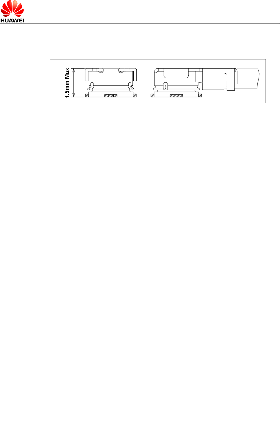
Figure 3-30 shows the specifications of 1.13 mm coaxial cable mating the
recommended RF connector.
Figure 3-30 Specifications of 1.13 mm coaxial cable mating with the RF connector
HUAWEI MU736 HSPA+ M.2 Module
Hardware Guide
Description of the Application Interfaces
Issue 05 (2014-01-14)
Huawei Proprietary and Confidential
Copyright © Huawei Technologies Co., Ltd.
42
Figure 3-31 shows the connection between the RF connector and the 1.13 mm cable.
Figure 3-31 Connection between the RF connector and the 1.13 mm cable
HUAWEI MU736 HSPA+ M.2 Module
Hardware Guide
RF Specifications
Issue 05 (2014-01-14)
Huawei Proprietary and Confidential
Copyright © Huawei Technologies Co., Ltd.
43
4 RF Specifications
4.1 About This Chapter
This chapter describes the RF specifications of the MU736 module, including:
- Operating Frequencies
- Conducted RF Measurement
- Conducted Rx Sensitivity and Tx Power
- Antenna Design Requirements
4.2 Operating Frequencies
Table 4-1 shows the RF bands supported by MU736.
Table 4-1 RF bands
Operating Band
Tx
Rx
UMTS Band I
1920 MHz–1980 MHz
2110 MHz–2170 MHz
UMTS Band II
1850 MHz–1910 MHz
1930 MHz–1990 MHz
UMTS Band IV(AWS)
1710 MHz–1755 MHz
2110 MHz–2155 MHz
UMTS Band V
824 MHz–849 MHz
869 MHz–894 MHz
UMTS Band VIII
880 MHz–915 MHz
925 MHz–960 MHz
GSM 850
824 MHz–849 MHz
869 MHz–894 MHz
GSM 900
880 MHz–915 MHz
925 MHz–960 MHz
GSM 1800(DCS)
1710 MHz–1785 MHz
1805 MHz–1880 MHz
GSM 1900(PCS)
1850 MHz–1910 MHz
1930 MHz–1990 MHz
GPS
-
1574.42 MHz–1576.42 MHz
HUAWEI MU736 HSPA+ M.2 Module
Hardware Guide
RF Specifications
Issue 05 (2014-01-14)
Huawei Proprietary and Confidential
Copyright © Huawei Technologies Co., Ltd.
44
4.3 Conducted RF Measurement
4.3.1 Test Environment
Test instrument
R&S CMU200, Agilent E5515C, GSS6700
Power supply
Keithley 2303, Agilent 66319
RF cable for testing
Rosenberger Precision Microwave Cable
Murata coaxial cable
MXHP32HP1000
- The compensation for different frequency bands relates to the cable and the test
environment.
- The instrument compensation needs to be set according to the actual cable conditions.
4.3.2 Test Standards
Huawei modules meet 3GPP TS 51.010-1 and 3GPP TS 34.121-1 test standards.
Each module passes strict tests at the factory and thus the quality of the modules is
guaranteed.
4.4 Conducted Rx Sensitivity and Tx Power
4.4.1 Conducted Receive Sensitivity
The conducted receive sensitivity is a key parameter that indicates the receiver
performance of MU736.
The 3GPP Protocol Claim column in Table 4-2 lists the required minimum values,
and the Test Value column lists the tested values of MU736.
Table 4-2 MU736 conducted Rx sensitivity (Unit: dBm)
Item
3GPP Protocol
Claim (dBm)
MU736 Test Value (dBm)
Min.
Typ.
Max.
GSM850
GMSK (CS1, BLER <
10%)
< –102
-
-
–108
8PSK (MCS5, BLER <
10%)
< –98
-
-
–101
GSM900
GMSK (CS1, BLER <
10%)
< –102
-
-
–108
8PSK (MCS5, BLER <
10%)
< –98
-
-
–101
HUAWEI MU736 HSPA+ M.2 Module
Hardware Guide
RF Specifications
Issue 05 (2014-01-14)
Huawei Proprietary and Confidential
Copyright © Huawei Technologies Co., Ltd.
45
Item
3GPP Protocol
Claim (dBm)
MU736 Test Value (dBm)
Min.
Typ.
Max.
GSM1800
GMSK (CS1, BLER <
10%)
< –102
-
-
–108
8PSK (MCS5, BLER <
10%)
< –98
-
-
–101
GSM1900
GMSK (CS1, BLER <
10%)
< –102
-
-
–108
8PSK (MCS5, BLER <
10%)
< –98
-
-
–101
Band I (BER < 0.1%)
< –106.7
-
-
–108
Band II (BER < 0.1%)
< –104.7
-
-
–108
Band IV (BER < 0.1%)
< –106.7
-
-
–108
Band VIII (BER < 0.1%)
< –103.7
-
-
–108
Band V (BER < 0.1%)
< –104.7
-
-
–108
Table 4-3 MU736 GPS specifications
TTFF
Cold start
43s@–130 dBm
Warm start
43s@–130 dBm
Hot Start
3s@–130 dBm
Sensitivity
Cold start
–144 dBm
Tracking
–158 dBm
The test values are the average of some test samples.
4.4.2 Conducted Transmit Power
The conducted transmit power is another indicator that measures the performance of
MU736. The conducted transmit power refers to the maximum power that the module
tested at the antenna port can transmit. According to the 3GPP protocol, the required
transmit power varies with the power class.
Table 4-4 lists the required ranges of the conducted transmit power of MU736. The
tested values listed in the Test Value column must range from the minimum power to
the maximum power.
HUAWEI MU736 HSPA+ M.2 Module
Hardware Guide
RF Specifications
Issue 05 (2014-01-14)
Huawei Proprietary and Confidential
Copyright © Huawei Technologies Co., Ltd.
46
Table 4-4 MU736 conducted Tx power (Unit: dBm)
Item
3GPP Protocol
Claim (dBm)
MU736 Test Value (dBm)
Min.
Typ.
Max.
GSM850
GMSK (1Tx Slot)
31 to 35
31.5
32.5
33.5
8PSK (1Tx Slot)
24 to 30
26
27
28
GSM900
GMSK (1Tx Slot)
31 to 35
31.5
32.5
33.5
8PSK (1Tx Slot)
24 to 30
26
27
28
GSM1800
GMSK (1Tx Slot)
28 to 32
28.5
29.5
30.5
8PSK (1Tx Slot)
23 to 29
25
26
27
GSM1900
GMSK (1Tx Slot)
28 to 32
28.5
29.5
30.5
8PSK (1Tx Slot)
23 to 29
25
26
27
Band I
21 to 25
22.5
23.5
24.5
Band II
21 to 25
22.5
23.5
24.5
Band IV
21 to 25
22.5
23.5
24.5
Band VIII
21 to 25
22.5
23.5
24.5
Band V
21 to 25
22.5
23.5
24.5
4.5 Antenna Design Requirements
4.5.1 Antenna Design Indicators
Antenna Efficiency
Antenna efficiency is the ratio of the input power to the radiated or received power of
an antenna. The radiated power of an antenna is always lower than the input power
due to the following antenna losses: return loss, material loss, and coupling loss. The
efficiency of an antenna relates to its electrical dimensions. To be specific, the
antenna efficiency increases with the electrical dimensions. In addition, the
transmission cable from the antenna port of MU736 to the antenna is also part of the
antenna. The cable loss increases with the cable length and the frequency. It is
recommended that the cable loss be as low as possible, for example, U.FL-LP-088
made by HRS.
The following antenna efficiency (free space) is recommended for MU736 to ensure
high radio performance of the module:
- Efficiency of the primary antenna: ≥ 40% (below 960 MHz); ≥ 50% (over 1710
MHz)
- Efficiency of the diversity antenna: ≥ half of the efficiency of the primary antenna
in receiving band

HUAWEI MU736 HSPA+ M.2 Module
Hardware Guide
RF Specifications
Issue 05 (2014-01-14)
Huawei Proprietary and Confidential
Copyright © Huawei Technologies Co., Ltd.
47
- Efficiency of the GPS antenna: ≥ 50%
In addition, the efficiency should be tested with the transmission cable.
S11 or VSWR
S11 indicates the degree to which the input impedance of an antenna matches the
reference impedance (50 ohm). S11 shows the resonance feature and impedance
bandwidth of an antenna. Voltage standing wave ratio (VSWR) is another expression
of S11. S11 relates to the antenna efficiency. S11 can be measured with a vector
analyzer.
The following S11 values are recommended for the antenna of MU736:
- S11 of the primary antenna ≤ –6 dB
- S11 of the diversity antenna ≤ –6 dB
- S11 of the GPS antenna ≤ –10 dB
In addition, S11 is less important than the efficiency, and S11 has weak correlation to
the wireless performance.
Isolation
For a wireless device with multiple antennas, the power of different antennas is
coupled with each other. Antenna isolation is used to measure the power coupling.
The power radiated by an antenna might be received by an adjacent antenna, which
decreases the antenna radiation efficiency and affects the running of other devices. To
avoid this problem, evaluate the antenna isolation as sufficiently as possible at the
early stage of antenna design.
Antenna isolation depends on the following factors:
- Distance between antennas
- Antenna type
- Antenna direction
The primary antenna must be placed as near as possible to the MU736 to minimize
the cable length. The diversity antenna needs to be installed perpendicularly to the
primary antenna. The diversity antenna can be placed farther away from the MU736.
Antenna isolation can be measured with a two-port vector network analyzer.
The following antenna isolation is recommended for the antennas on laptops:
- Isolation between the primary and diversity antennas ≤ –12 dB
- Isolation between the primary antenna and the GPS antenna ≤ –15 dB
- Isolation between the primary antenna and the Wi-Fi antenna ≤ –15 dB
Polarization
The polarization of an antenna is the orientation of the electric field vector that rotates
with time in the direction of maximum radiation.
The linear polarization is recommended for the antenna of MU736.

HUAWEI MU736 HSPA+ M.2 Module
Hardware Guide
RF Specifications
Issue 05 (2014-01-14)
Huawei Proprietary and Confidential
Copyright © Huawei Technologies Co., Ltd.
48
Envelope Correlation Coefficient
The envelope correlation coefficient indicates the correlation between different
antennas in a multi-antenna system (primary antenna, diversity antenna, and MIMO
antenna). The correlation coefficient shows the similarity of radiation patterns, that is,
amplitude and phase of the antennas. The ideal correlation coefficient of a diversity
antenna system or a MIMO antenna system is 0. A small value of the envelope
correlation coefficient between the primary antenna and the diversity antenna
indicates a high diversity gain. The envelope correlation coefficient depends on the
following factors:
- Distance between antennas
- Antenna type
- Antenna direction
The antenna correlation coefficient differs from the antenna isolation. Sufficient
antenna isolation does not represent a satisfactory correlation coefficient. For this
reason, the two indicators need to be evaluated separately.
For the antennas on laptops, the recommended envelope correlation coefficient
between the primary antenna and the diversity antenna is smaller than 0.5.
Radiation Pattern
The radiation pattern of an antenna reflects the radiation features of the antenna in the
remote field region. The radiation pattern of an antenna commonly describes the
power or field strength of the radiated electromagnetic waves in various directions
from the antenna. The power or field strength varies with the angular coordinates (θ
and φ), but is independent of the radial coordinates.
The radiation pattern of half wave dipole antennas is omnidirectional in the horizontal
plane, and the incident waves of base stations are often in the horizontal plane. For
this reason, the receiving performance is optimal.
The following radiation patterns are recommended for the antenna of MU736:
Primary/Diversity/GPS/WIFI antenna: omnidirectional.
In addition, the diversity antenna’s pattern should be complementary with the primary
antenna’s pattern.
Gain and Directivity
The radiation pattern of an antenna represents the field strength of the radiated
electromagnetic waves in all directions, but not the power density that the antenna
radiates in the specific direction. The directivity of an antenna, however, measures the
power density that the antenna radiates.
Gain, as another important parameter of antennas, correlates closely to the directivity.
The gain of an antenna takes both the directivity and the efficiency of the antenna into
account. The appropriate antenna gain prolongs the service life of relevant batteries.
The following antenna gain is recommended for MU736:
- Gain of the primary antenna ≤ 2.5 dBi
- Gain of the diversity antenna ≤ 2.5 dBi
HUAWEI MU736 HSPA+ M.2 Module
Hardware Guide
RF Specifications
Issue 05 (2014-01-14)
Huawei Proprietary and Confidential
Copyright © Huawei Technologies Co., Ltd.
49
- The antenna consists of the antenna body and the relevant RF transmission cable. Take the
RF transmission cable into account when measuring any of the preceding antenna
indicators.
- Huawei cooperates with various famous antenna suppliers who are able to make
suggestions on antenna design, for example, Amphenol, Skycross, etc.
4.5.2 Interference
Besides the antenna performance, the interference on the user board also affects the
radio performance (especially the TIS) of the module. To guarantee high performance
of the module, the interference sources on the user board must be properly controlled.
On the user board, there are various interference sources, such as the LCD, CPU,
audio circuits, and power supply. All the interference sources emit interference signals
that affect the normal operation of the module. For example, the module sensitivity
can be decreased due to interference signals. Therefore, during the design, you need
to consider how to reduce the effects of interference sources on the module. You can
take the following measures: Use an LCD with optimized performance; shield the LCD
interference signals; shield the signal cable of the board; or design filter circuits.
Huawei is able to make technical suggestions on radio performance improvement of
the module.
4.5.3 GSM/WCDMA/GPS Antenna Requirements
The antenna for MU736 must fulfill the following requirements:
GSM/WCDMA/GPS Antenna Requirements
Frequency range
Depending on frequency band(s) provided by the network
operator, the customer must use the most suitable
antenna for that/those band(s)
Bandwidth
70 MHz in GSM850
80 MHz in GSM900
170 MHz in DCS
140 MHz in PCS
70 MHZ in WCDMA850 (25 MHz for diversity antenna)
80 MHz in WCDMA900 (35 MHz for diversity antenna)
445 MHz in WCDMA1700 (AWS) (45 MHz for diversity
antenna)
140 MHz in WCDMA1900 (60 MHz for diversity antenna)
250 MHz in WCDMA2100 (60 MHz for diversity antenna)
2 MHz in GPS
Gain
≤ 2.5 dBi
Impedance
50 Ω
VSWR absolute max
≤ 3:1 (≤ 2:1 for GPS antenna)

HUAWEI MU736 HSPA+ M.2 Module
Hardware Guide
RF Specifications
Issue 05 (2014-01-14)
Huawei Proprietary and Confidential
Copyright © Huawei Technologies Co., Ltd.
50
GSM/WCDMA/GPS Antenna Requirements
VSWR recommended
≤ 2:1 (≤ 1.5:1 for GPS antenna)
4.5.4 Radio Test Environment
The antenna efficiency, antenna gain, radiation pattern, total radiated power (TRP),
and total isotropic sensitivity (TIS) can be tested in a microwave testing chamber.
Huawei has a complete set of OTA test environments (SATIMO microwave testing
chambers and ETS microwave testing chambers). The testing chambers are certified
by professional organizations and are applicable to testing at frequencies ranging
from 380 MHz to 6 GHz. The test items are described as follows.
Passive Tests
- Antenna efficiency
- Gain
- Pattern shape
- Envelope correlation coefficient
Active Tests
- TRP: GSM, WCDMA systems
- TIS: GSM, WCDMA systems
Figure 4-1 shows the SATIMO microwave testing chamber.
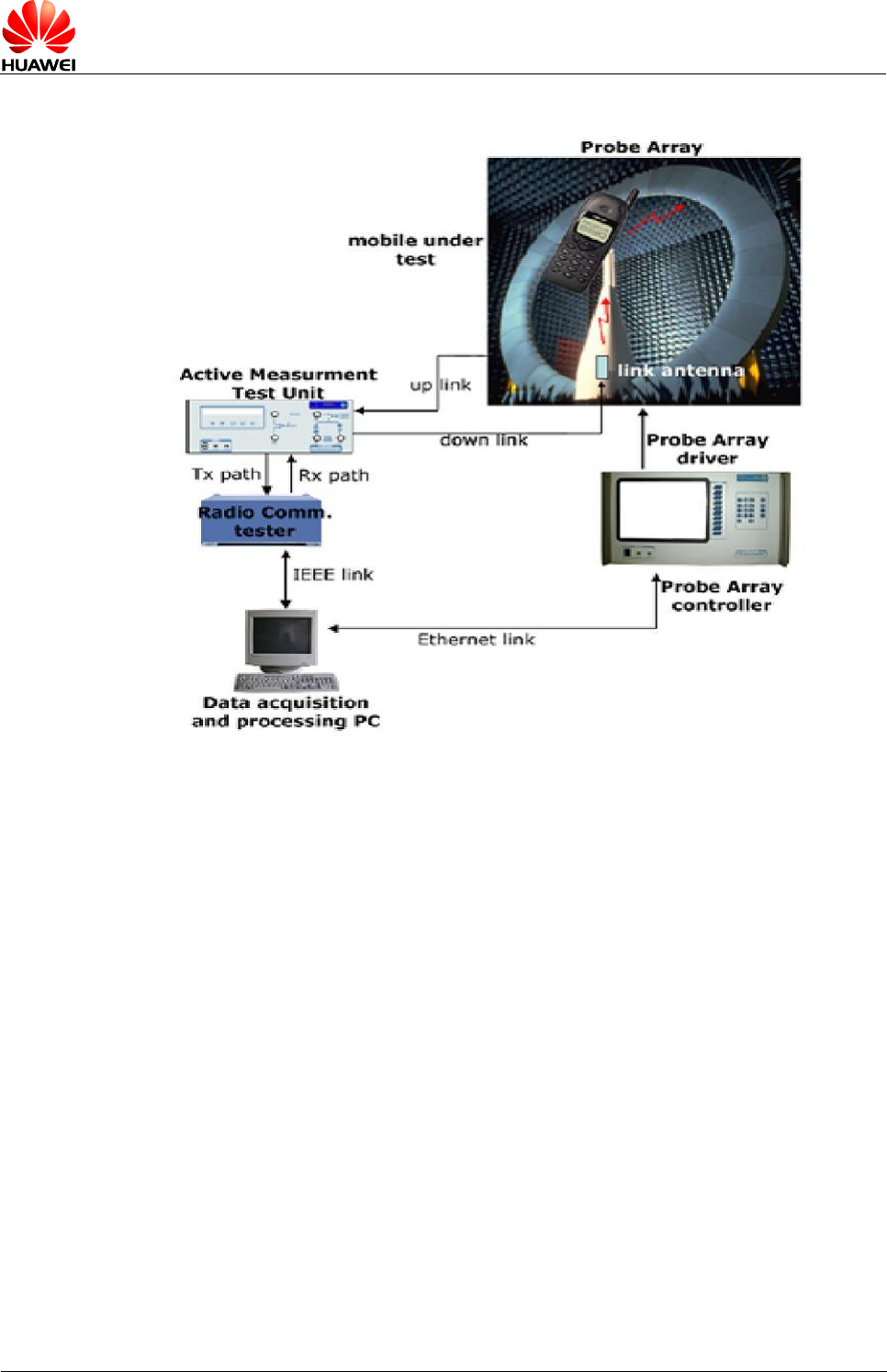
HUAWEI MU736 HSPA+ M.2 Module
Hardware Guide
RF Specifications
Issue 05 (2014-01-14)
Huawei Proprietary and Confidential
Copyright © Huawei Technologies Co., Ltd.
51
Figure 4-1 SATIMO microwave testing chamber
HUAWEI MU736 HSPA+ M.2 Module
Hardware Guide
Electrical and Reliability Features
Issue 05 (2014-01-14)
Huawei Proprietary and Confidential
Copyright © Huawei Technologies Co., Ltd.
52
5 Electrical and Reliability Features
5.1 About This Chapter
This chapter describes the electrical and reliability features of the interfaces in the
MU736 module, including:
- Absolute Ratings
- Operating and Storage Temperatures and Humidity
- Electrical Features of Application Interfaces
- Power Supply Features
- Reliability Features
- EMC and ESD Features
5.2 Absolute Ratings
Table 5-1 lists the absolute ratings for the MU736 module. Using the MU736 module
beyond these conditions may result in permanent damage to the module.
Table 5-1 Absolute ratings for the MU736 module
Symbol
Specification
Min.
Max.
Unit
3.3 V
External power voltage
–0.3
5.5
V
HUAWEI MU736 HSPA+ M.2 Module
Hardware Guide
Electrical and Reliability Features
Issue 05 (2014-01-14)
Huawei Proprietary and Confidential
Copyright © Huawei Technologies Co., Ltd.
53
5.3 Operating and Storage Temperatures and Humidity
Table 5-2 lists the operating and storage temperatures and humidity for the MU736
module.
Table 5-2 operating and storage temperatures and humidity for the MU736 module
Specification
Min.
Max.
Unit
Normal working temperatures[1]
–10
+55
°C
Extended temperatures[2]
–20
+70
°C
Ambient temperature for storage
–40
+85
°C
Moisture
5
95
%
[1]: When the MU736 module works at this temperature, all its RF indexes comply with the
3GPP TS 45.005 specifications.
[2]: When the MU736 module works at this temperature, NOT all its RF indexes comply with the
3GPP TS 45.005 specifications.
5.4 Electrical Features of Application Interfaces
Table 5-3 Electrical features of Digital Pins
Parameter
Description
Min.
Max.
Unit
BodySAR_N
VIH
1.26
3.6
V
VIL
–0.2
0.3
V
RESET
VIH
1.26
2.1
V
VIL
–0.2
0.3
V
Power_On_Off
VIH
1.26
3.6
V
VIL
–0.2
0.3
V
W_DISABLE
VIH
1.26
3.6
V
VIL
–0.2
0.3
V
GPS_DISABLE
VIH
1.26
3.6
V
VIL
–0.2
0.3
V
SIM_DET
VIH
1.26
2.1
V
VIL
–0.2
0.3
V
HUAWEI MU736 HSPA+ M.2 Module
Hardware Guide
Electrical and Reliability Features
Issue 05 (2014-01-14)
Huawei Proprietary and Confidential
Copyright © Huawei Technologies Co., Ltd.
54
Table 5-4 Electrical features of Digital Pins in the I/O supply domain of the USIM
Interface
Parameter
Description
Min.
Max.
Note
Unit
VIH
High-level
input voltage
0.7 x
VDDP_USIM
3.3
VDDP_USIM=1.8 V or
2.9 V
V
VIL
Low-level
input voltage
0
0.2 x
VDDP_USIM
VDDP_USIM=1.8 V or
2.9 V
V
VOH
High-level
output
voltage
0.7 x
VDDP_USIM
3.3
VDDP_USIM=1.8 V or
2.9 V, IOL=–1.0 mA
V
VOL
Low-level
output
voltage
0
0.2 x
VDDP_USIM
VDDP_USIM=1.8 V or
2.9 V, IOL=+1.0 mA
V
Ileak
Input/Output
leakage
current
-
±0.7
0.2V < VIN < VIHmax
μA
Table 5-5 Electrical features of Digital Pins of the ANT_TUNER Interface
Parameter
Description
Min.
Max.
Note
Unit
VOH
High-level
output
voltage
1.26
2
-
V
VOL
Low-level
output
voltage
0
0.15
-
V
5.5 Power Supply Features
5.5.1 Input Power Supply
Table 5-6 lists the requirements for input power of the MU736 module.
Table 5-6 Requirements for input power for the MU736 module
Parameter
Min.
Typ.
Max.
Ripple
Unit
3.3 V
3.135
3.3
4.4
0.05
V
HUAWEI MU736 HSPA+ M.2 Module
Hardware Guide
Electrical and Reliability Features
Issue 05 (2014-01-14)
Huawei Proprietary and Confidential
Copyright © Huawei Technologies Co., Ltd.
55
Figure 5-1 Power Supply During Burst Emission
The minimum value of the power supply must be guaranteed during the burst (with 2. 5 A Peak
in GPRS or EGPRS mode).
Table 5-7 Requirements for input current of the MU736 module
Power
Peak (Maximum)
Normal (Maximum)
3.3 V
2500 mA
1100 mA
5.5.2 Power Consumption
The power consumption of MU736 in different scenarios are respectively listed in
Table 5-8 to Table 5-12 .
The power consumption listed in this section is tested when the power supply of
MU736 module is normal voltage (3.3 V), and all of test values are measured at room
temperature.
Table 5-8 Averaged power off DC power consumption of MU736
Description
Test Value (uA)
Notes/Configuration
Typical
Power off
50
Normal voltage (3.3 V) is ON and
Power_On_Off pin is pulled low.
HUAWEI MU736 HSPA+ M.2 Module
Hardware Guide
Electrical and Reliability Features
Issue 05 (2014-01-14)
Huawei Proprietary and Confidential
Copyright © Huawei Technologies Co., Ltd.
56
Table 5-9 Averaged standby DC power consumption of MU736 (WCDMA/HSDPA/GSM)
Description
Bands
Test Value (mA)
Notes/Configuration
Typical
Sleep
HSPA+/WCDMA
(sleep)
UMTS bands
2.3
Module is powered up.
DRX cycle=8 (2.56s)
Module is registered on the
network.
USB is in suspend.
GPRS/EDGE
(sleep)
GSM bands
2.3
Module is powered up.
MFRMS=5 (1.175s)
Module is registered on the
network.
USB is in suspend.
Radio Off
(sleep)
All bands
1.6
Module is powered up.
RF is disabled.
USB is in suspend.
Idle
HSPA+/WCDMA
(idle)
UMTS bands
30
Module is powered up.
DRX cycle=8 (2.56s)
Module is registered on the
network, and no data is
transmitted.
USB is in active.
GPRS/EDGE
(idle)
GSM bands
30
Module is powered up.
MFRMS=5 (1.175s)
Module is registered on the
network.
no data is transmitted.
USB is in active.
Radio Off
(idle)
All bands
30
Module is powered up.
RF is disabled.
USB is in active.
Table 5-10 Averaged Data Transmission DC power consumption of MU736
(WCDMA/HSDPA)
Description
Band
Test Value (mA)
Notes/Configuration
Typical
WCDMA
Band I
(IMT2100)
190
0 dBm Tx Power
245
10 dBm Tx Power
HUAWEI MU736 HSPA+ M.2 Module
Hardware Guide
Electrical and Reliability Features
Issue 05 (2014-01-14)
Huawei Proprietary and Confidential
Copyright © Huawei Technologies Co., Ltd.
57
Description
Band
Test Value (mA)
Notes/Configuration
Typical
710
23.5 dBm Tx Power
Band II
(PCS 1900)
180
0 dBm Tx Power
245
10 dBm Tx Power
790
23.5 dBm Tx Power
Band IV
(AWS)
180
0 dBm Tx Power
220
10 dBm Tx Power
690
23.5 dBm Tx Power
Band V
(850 MHz)
180
0 dBm Tx Power
220
10 dBm Tx Power
680
23.5 dBm Tx Power
Band VIII
(900 MHz)
180
0 dBm Tx Power
240
10 dBm Tx Power
760
23.5 dBm Tx Power
HSDPA
Band I
(IMT2100)
195
0 dBm Tx Power
260
10 dBm Tx Power
740
23.5 dBm Tx Power
Band II
(PCS 1900)
195
0 dBm Tx Power
255
10 dBm Tx Power
790
23.5 dBm Tx Power
Band IV
(AWS)
190
0 dBm Tx Power
250
10 dBm Tx Power
690
23.5 dBm Tx Power
Band V
(850 MHz)
195
0 dBm Tx Power
245
10 dBm Tx Power
690
23.5 dBm Tx Power
Band VIII
(900 MHz)
195
0 dBm Tx Power
255
10 dBm Tx Power
730
23.5 dBm Tx Power
HUAWEI MU736 HSPA+ M.2 Module
Hardware Guide
Electrical and Reliability Features
Issue 05 (2014-01-14)
Huawei Proprietary and Confidential
Copyright © Huawei Technologies Co., Ltd.
58
Table 5-11 Averaged DC power consumption of MU736 (GPRS/EDGE)
Description
Test Value (mA)
PCL
Notes/Configuration
Typical
GPRS850
265
5
1 Up/1 Down
385
2 Up/1 Down
535
4 Up/1 Down
145
10
1 Up/1 Down
230
2 Up/1 Down
380
4 Up/1 Down
GPRS900
270
5
1 Up/1 Down
390
2 Up/1 Down
550
4 Up/1 Down
145
10
1 Up/1 Down
230
2 Up/1 Down
395
4 Up/1 Down
GPRS1800
175
0
1 Up/1 Down
225
2 Up/1 Down
265
4 Up/1 Down
80
10
1 Up/1 Down
105
2 Up/1 Down
140
4 Up/1 Down
GPRS1900
185
0
1 Up/1 Down
240
2 Up/1 Down
280
4 Up/1 Down
80
10
1 Up/1 Down
105
2 Up/1 Down
145
4 Up/1 Down
EDGE850
185
8
1 Up/1 Down
280
2 Up/1 Down
430
4 Up/1 Down
100
15
1 Up/1 Down
145
2 Up/1 Down
HUAWEI MU736 HSPA+ M.2 Module
Hardware Guide
Electrical and Reliability Features
Issue 05 (2014-01-14)
Huawei Proprietary and Confidential
Copyright © Huawei Technologies Co., Ltd.
59
Description
Test Value (mA)
PCL
Notes/Configuration
Typical
220
4 Up/1 Down
EDGE900
190
8
1 Up/1 Down
295
2 Up/1 Down
455
4 Up/1 Down
100
15
1 Up/1 Down
150
2 Up/1 Down
230
4 Up/1 Down
EDGE1800
150
2
1 Up/1 Down
240
2 Up/1 Down
360
4 Up/1 Down
100
10
1 Up/1 Down
150
2 Up/1 Down
230
4 Up/1 Down
EDGE1900
150
2
1 Up/1 Down
230
2 Up/1 Down
360
4 Up/1 Down
100
10
1 Up/1 Down
150
2 Up/1 Down
230
4 Up/1 Down
All power consumption test configuration can be referenced by GSM Association Official
Document TS.09: Battery Life Measurement and Current Consumption Technique.
- Test condition: For Max Tx power ,see 4.4.2 Conducted Transmit Power, they are listed in
Table 4-4 ; for Max data throughput, see 2.2 Function Overview, they are listed in Table 2-1
Features.
Table 5-12 Averaged GPS operation DC power consumption of MU736
Description
Test Value (mA)
Notes/Configuration
Typical
GPS fixing
100
RF is disabled;
HUAWEI MU736 HSPA+ M.2 Module
Hardware Guide
Electrical and Reliability Features
Issue 05 (2014-01-14)
Huawei Proprietary and Confidential
Copyright © Huawei Technologies Co., Ltd.
60
Description
Test Value (mA)
Notes/Configuration
Typical
GPS tracking
100
USB is in active;
The Rx power of GPS is –130 dBm.
5.6 Reliability Features
Table 5-13 lists the test conditions and results of the reliability of the MU736 module.
Table 5-13 Test conditions and results of the reliability of the MU736 module
Item
Test Condition
Standard
Sample size
Results
Stress
Low-temperature
storage
Temperature: –40ºC
Operation mode: no
power, no package
Test duration: 24 h
JESD22-
A119-C
3 pcs/group
Visual inspection:
ok
Function test: ok
RF specification: ok
High-temperature
storage
Temperature: 85ºC
Operation mode: no
power, no package
Test duration: 24 h
JESD22-
A103-C
3 pcs/group
Visual inspection:
ok
Function test: ok
RF specification: ok
Low-temperature
operating
Temperature: –20ºC
Operation mode:
working with service
connected
Test duration: 24 h
IEC6006
8-2-1
3 pcs/group
Visual inspection:
ok
Function test: ok
RF specification: ok
High-temperature
operating
Temperature: 70ºC
Operation mode:
working with service
connected
Test duration: 24 h
JESD22-
A108-C
3 pcs/group
Visual inspection:
ok
Function test: ok
RF specification: ok
Damp heat cycling
High temperature:
55ºC
Low temperature:
25ºC
Humidity: 95%±3%
Operation mode:
working with service
connected
Test duration: 6
cycles; 12 h+12
h/cycle
JESD22-
A101-B
3 pcs/group
Visual inspection:
ok
Function test: ok
RF specification: ok
HUAWEI MU736 HSPA+ M.2 Module
Hardware Guide
Electrical and Reliability Features
Issue 05 (2014-01-14)
Huawei Proprietary and Confidential
Copyright © Huawei Technologies Co., Ltd.
61
Item
Test Condition
Standard
Sample size
Results
Thermal shock
Low temperature:
–40º
High temperature:
85ºC
Temperature change
interval: < 20s
Operation mode:
working with service
connected
Test duration: 100
cycles; 15 min+15
min/cycle
JESD22-
A106-B
3 pcs/group
Visual inspection:
ok
Function test: ok
RF specification: ok
Stress
Salty fog test
Temperature: 35°C
Density of the NaCl
solution: 5%±1%
Operation mode: no
power, no package
Test duration:
Spraying period: 8 h
Exposing period after
removing the salty fog
environment: 16 h
JESD22-
A107-B
3 pcs/group
Visual inspection:
ok
Function test: ok
RF specification: ok
Sine vibration
Frequency range: 5
Hz to 200 Hz
Acceleration: 1 Grms
Frequency scan rate:
0.5 oct/min
Operation mode:
working with service
connected
Test duration: 3 axial
directions. 2 h for
each axial direction.
Operation mode:
working with service
connected
JESD22-
B103-B
3 pcs/group
Visual inspection:
ok
Function test: ok
RF specification: ok
HUAWEI MU736 HSPA+ M.2 Module
Hardware Guide
Electrical and Reliability Features
Issue 05 (2014-01-14)
Huawei Proprietary and Confidential
Copyright © Huawei Technologies Co., Ltd.
62
Item
Test Condition
Standard
Sample size
Results
Shock test
Half-sine wave shock
Peak acceleration: 30
Grms
Shock duration: 11 ms
Operation mode:
working with service
connected
Test duration: 6 axial
directions. 3 shocks
for each axial
direction.
Operation mode:
working with service
connected
JESD-B1
04-C
3 pcs/group
Visual inspection:
ok
Function test: ok
RF specification: ok
Stress
Drop test
0.8 m in height. Drop
the module on the
marble terrace with
one surface facing
downwards, six
surfaces should be
tested.
Operation mode: no
power, no package
IEC6006
8-2-32
3 pcs/group
Visual inspection:
ok
Function test: ok
RF specification: ok
Life
High temperature
operating life
Temperature: 70ºC
Operation mode:
working with service
connected
Test duration: 168 h,
336 h, 500 h, 1000 h
for inspection point
JESD22-
A108-B
50
pcs/group
Visual inspection:
ok
Function test: ok
RF specification: ok
High temperature
& high humidity
High temperature:
85ºC
Humidity: 85%
Operation mode:
powered on and no
working
Test duration: 168 h,
336 h, 500 h, 1000 h
for inspection point
JESD22-
A110-B
50
pcs/group
Visual inspection:
ok
Function test: ok
RF specification: ok
Cross section: ok
HUAWEI MU736 HSPA+ M.2 Module
Hardware Guide
Electrical and Reliability Features
Issue 05 (2014-01-14)
Huawei Proprietary and Confidential
Copyright © Huawei Technologies Co., Ltd.
63
Item
Test Condition
Standard
Sample size
Results
Temperature cycle
High temperature:
85ºC
Low temperature:
–40ºC
Temperature change
slope: 6ºC/min
Operation mode: no
power
Test duration: 168 h,
336 h, 500 h, 1000 h
for inspection point
JESD22-
A104-C
50
pcs/group
Visual inspection:
ok
Function test: ok
RF specification: ok
Cross section: ok
ESD
HBM (Human
Body Model)
1 kV (Class 1 B)
Operation mode: no
power
JESD22-
A114-D
3 pcs/group
Visual inspection:
ok
Function test: ok
RF specification: ok
ESD with DVK (or
embedded in the
host)
Contact Voltage: ±2
kV, ±4 kV
Air Voltage: ±2 kV, ±4
kV, ±8 kV
Operation mode:
working with service
connected
IEC6100
0-4-2
2 pcs
Visual inspection:
ok
Function test: ok
RF specification: ok
Groups ≥ 2
5.7 EMC and ESD Features
The following are the EMC design comments:
- Attention should be paid to static control in the manufacture, assembly, packaging,
handling, and storage process to reduce electrostatic damage to HUAWEI
module.
- RSE (Radiated Spurious Emission) may exceed the limit defined by EN301489 if
the antenna port is protected by TVS (Transient Voltage Suppressor), which is
resolved by making some adjustments on RF match circuit.
- TVS should be added on the USB port for ESD protection, and the parasitic
capacitance of TVS on D+/D- signal should be less than 2 pF. Common-mode
inductor should be added in parallel on D+/D- signal.
- TVS should be added on the SIM interface for ESD protection. The parasitic
capacitance of TVS on SIM signal should be less than 10 pF.
- Resistors in parallel and a 10 nF capacitor should be added on RESET# and
Power_On_Off signal to avoid shaking, and the distance between the capacitor
and the related pin should be less than 100 mil.
HUAWEI MU736 HSPA+ M.2 Module
Hardware Guide
Electrical and Reliability Features
Issue 05 (2014-01-14)
Huawei Proprietary and Confidential
Copyright © Huawei Technologies Co., Ltd.
64
- PCB routing should be V-type rather than T-type for TVS.
- An integrated ground plane is necessary for EMC design.
The following are the requirements of ESD environment control:
- The electrostatic discharge protected area (EPA) must have an ESD floor whose
surface resistance and system resistance are greater than 1 x 10⁴ Ω while less
than 1 x 10⁹ Ω.
- The EPA must have a sound ground system without loose ground wires, and the
ground resistance must be less than 4 Ω.
- The workbench for handling ESD sensitive components must be equipped with
common ground points, the wrist strap jack, and ESD pad. The resistance
between the jack and common ground point must be less than 4 Ω. The surface
resistance and system resistance of the ESD pad must be less than 1 x 10⁹ Ω.
- The EPA must use the ESD two-circuit wrist strap, and the wrist strap must be
connected to the dedicated jack. The crocodile clip must not be connected to the
ground.
- The ESD sensitive components, the processing equipment, test equipment, tools,
and devices must be connected to the ground properly. The indexes are as
follows:
− Hard ground resistance < 4 Ω
− 1 x 10⁵ Ω ≤ Soft ground resistance < 1 x 10⁹ Ω
− 1 x 10⁵ Ω ≤ ICT fixture soft ground resistance < 1 x 10¹¹ Ω
− The electronic screwdriver and electronic soldering iron can be easily oxidized.
Their ground resistance must be less than 20 Ω.
- The parts of the equipment, devices, and tools that touch the ESD sensitive
components and moving parts that are close to the ESD sensitive components
must be made of ESD materials and have sound ground connection. The parts
that are not made of ESD materials must be handled with ESD treatment, such
as painting the ESD coating or ionization treatment (check that the friction voltage
is less than 100 V).
- Key parts in the production equipment (parts that touch the ESD sensitive
components or parts that are within 30 cm away from the ESD sensitive
components), including the conveyor belt, conveyor chain, guide wheel, and SMT
nozzle, must all be made of ESD materials and be connected to the ground
properly (check that the friction voltage is less than 100 V).
- Engineers that touch IC chips, boards, modules, and other ESD sensitive
components and assemblies must wear ESD wrist straps, ESD gloves, or ESD
finger cots properly. Engineers that sit when handling the components must all
wear ESD wrist straps.
- Noticeable ESD warning signs must be attached to the packages and placement
areas of ESD sensitive components and assemblies.
- Boards and IC chips must not be stacked randomly or be placed with other ESD
components.
- Effective shielding measures must be taken on the ESD sensitive materials that
are transported or stored outside the EPA.
The HUAWEI MU736 module does not include any protection against overvoltage.

HUAWEI MU736 HSPA+ M.2 Module
Hardware Guide
Mechanical Specifications
Issue 05 (2014-01-14)
Huawei Proprietary and Confidential
Copyright © Huawei Technologies Co., Ltd.
65
6 Mechanical Specifications
6.1 About This Chapter
This chapter describes the following aspects of the MU736 module:
- Dimensions of MU736
- Label
- Packing System
6.2 Dimensions of MU736
Figure 6-1 shows the dimensions of MU736 in details.
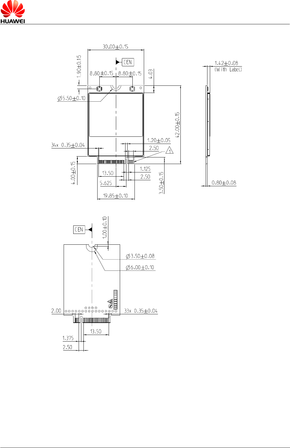
HUAWEI MU736 HSPA+ M.2 Module
Hardware Guide
Mechanical Specifications
Issue 05 (2014-01-14)
Huawei Proprietary and Confidential
Copyright © Huawei Technologies Co., Ltd.
66
Figure 6-1 Dimensions of MU736
TOP VIEW
BOTTOM VIEW
6.3 Label
There are two labels on the MU736.
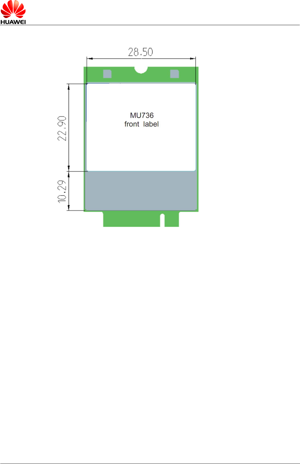
HUAWEI MU736 HSPA+ M.2 Module
Hardware Guide
Mechanical Specifications
Issue 05 (2014-01-14)
Huawei Proprietary and Confidential
Copyright © Huawei Technologies Co., Ltd.
67
Figure 6-2 Dimensions of label (front label)
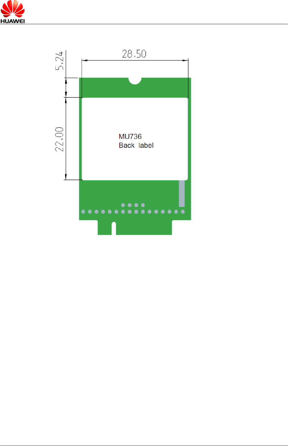
HUAWEI MU736 HSPA+ M.2 Module
Hardware Guide
Mechanical Specifications
Issue 05 (2014-01-14)
Huawei Proprietary and Confidential
Copyright © Huawei Technologies Co., Ltd.
68
Figure 6-3 Dimensions of label (back label)
6.4 Packing System
HUAWEI M.2 module uses five layers ESD pallet, anti-vibration foam and vacuum
packing into cartons.
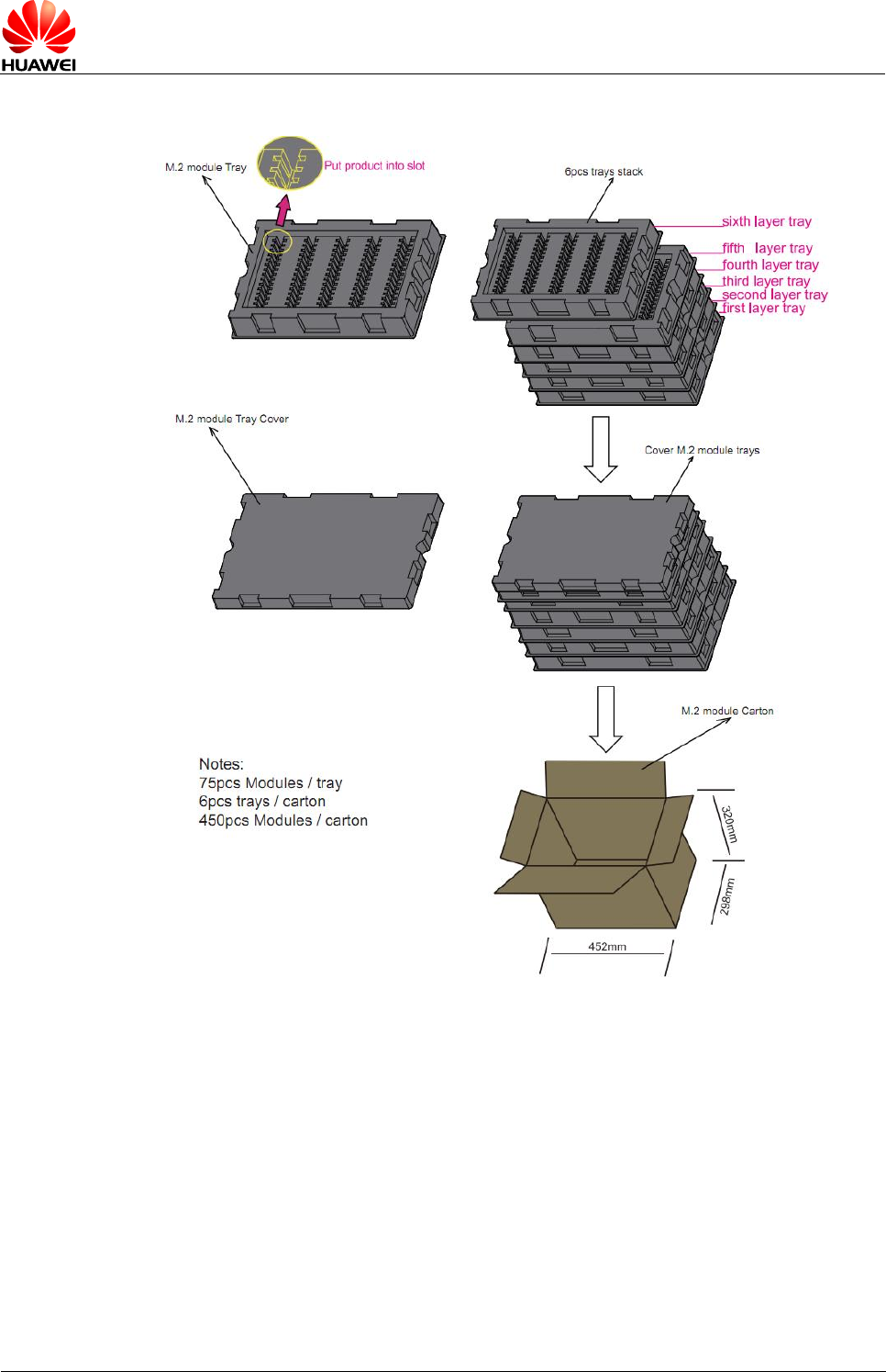
HUAWEI MU736 HSPA+ M.2 Module
Hardware Guide
Mechanical Specifications
Issue 05 (2014-01-14)
Huawei Proprietary and Confidential
Copyright © Huawei Technologies Co., Ltd.
69
Figure 6-4 Packet system
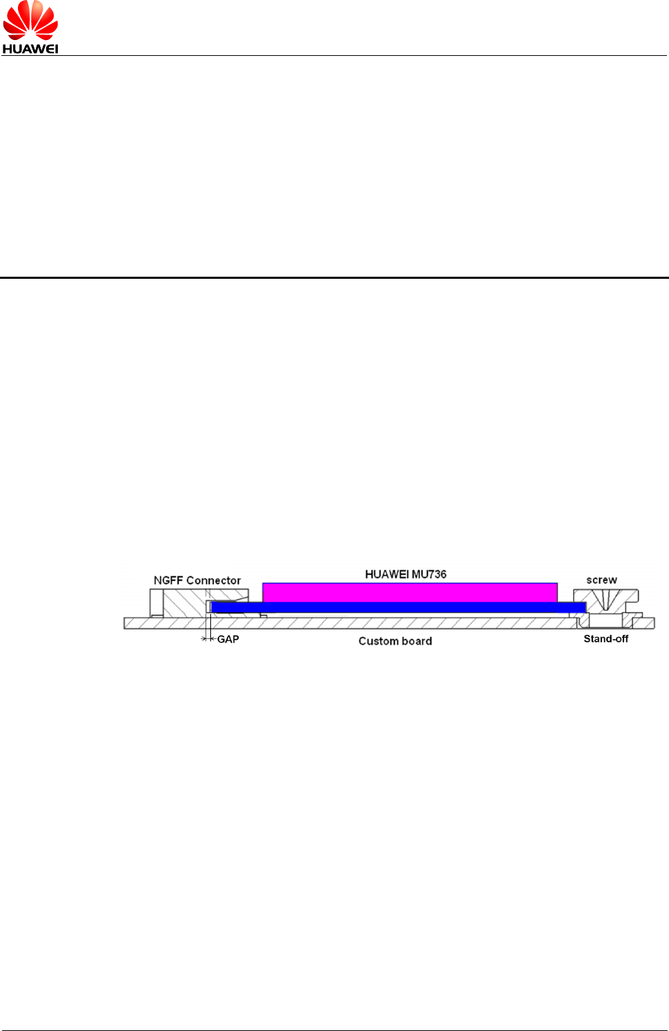
HUAWEI MU736 HSPA+ M.2 Module
Hardware Guide
Installation
Issue 05 (2014-01-14)
Huawei Proprietary and Confidential
Copyright © Huawei Technologies Co., Ltd.
70
7 Installation
7.1 About This Chapter
This chapter describes the assembly of MU736, including:
- Connect MU736 to Board
- Antenna Plug
7.2 Connect MU736 to Board
Figure 7-1 Install MU736
It refers to M.2 specification.
The module will need a mechanical retention at the end of the board. The module
specifies a 5.5 mm Dia. keep out zone at the end for attaching a screw.
The module Stand-off and mounting screw also serve as part of the module Electrical
Ground path. The Stand-off should be connected directly to the ground plane on the
platform. So that when the module is mounted and the mounting screw is screwed on
to hold the module in place, this will make the electrical ground connection from the
module to the platform ground plane.
The stand-off must provide a Thermal Ground Path. The design requirements for
thermal are a material with a minimum conductivity of 50 watts per meter Kelvin and
surface area of 22 Sq mm.
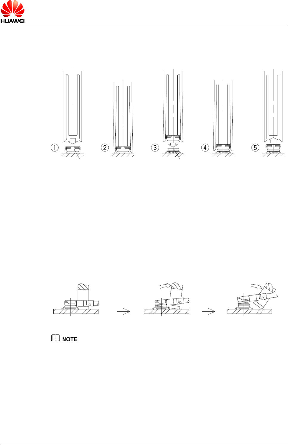
HUAWEI MU736 HSPA+ M.2 Module
Hardware Guide
Installation
Issue 05 (2014-01-14)
Huawei Proprietary and Confidential
Copyright © Huawei Technologies Co., Ltd.
71
7.3 Antenna Plug
Figure 7-2 Mating the plug
1. Align the mating tool or the mating end of the tool over the plug end of the cable
assembly.
2. Firmly place the tool over the plug until it is secured in the tool.
3. Place the plug cable assembly (held in the tool) over the corresponding
receptacle.
4. Assure that the plug and receptacle are aligned press-down perpendicular to the
mounting surface until both connectors are fully mated.
5. Remove the mating tool by pulling it up carefully.
Figure 7-3 Unmating the plug
- The extraction tool is recommended.
- Any attempt of unmating by pulling on the cable may result in damage and influence the
mechanical / electrical performance.
It is recommended that not to apply any pull forces after the bending of the cable, as
described in Figure 7-4 .
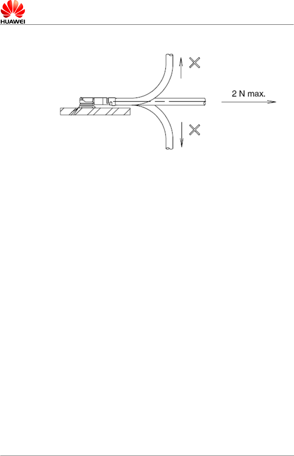
HUAWEI MU736 HSPA+ M.2 Module
Hardware Guide
Installation
Issue 05 (2014-01-14)
Huawei Proprietary and Confidential
Copyright © Huawei Technologies Co., Ltd.
72
Figure 7-4 Do not apply any pull forces after the bending of the cable
HUAWEI MU736 HSPA+ M.2 Module
Hardware Guide
Certifications
Issue 05 (2014-01-14)
Huawei Proprietary and Confidential
Copyright © Huawei Technologies Co., Ltd.
73
8 Certifications
8.1 About This Chapter
This chapter gives a general description of certifications of MU736.
8.2 Certifications
The certification of MU736 is testing now. Table 8-1 shows certifications the MU736 will be
implemented. For more demands, please contact us for more details about this information.
Table 8-1 Product Certifications
Certification
Model name
MU736
CE
FCC
CCC
NCC
A-TICK
Jate & Telec
IC
EU RoHS
JGPSSI
-
SGS RoHS
-
HUAWEI MU736 HSPA+ M.2 Module
Hardware Guide
Certifications
Issue 05 (2014-01-14)
Huawei Proprietary and Confidential
Copyright © Huawei Technologies Co., Ltd.
74
Certification
Model name
MU736
PVC-Free
-
GCF
PTCRB
Halogen-free

HUAWEI MU736 HSPA+ M.2 Module
Hardware Guide
Safety Information
Issue 05 (2014-01-14)
Huawei Proprietary and Confidential
Copyright © Huawei Technologies Co., Ltd.
75
9 Safety Information
Read the safety information carefully to ensure the correct and safe use of your
wireless device. Applicable safety information must be observed.
9.1 Interference
Power off your wireless device if using the device is prohibited. Do not use the
wireless device when it causes danger or interference with electric devices.
9.2 Medical Device
- Power off your wireless device and follow the rules and regulations set forth by
the hospitals and health care facilities.
- Some wireless devices may affect the performance of the hearing aids. For any
such problems, consult your service provider.
- Pacemaker manufacturers recommend that a minimum distance of 15 cm be
maintained between the wireless device and a pacemaker to prevent potential
interference with the pacemaker. If you are using an electronic medical device,
consult the doctor or device manufacturer to confirm whether the radio wave
affects the operation of this device.
9.3 Area with Inflammables and Explosives
To prevent explosions and fires in areas that are stored with inflammable and
explosive devices, power off your wireless device and observe the rules. Areas stored
with inflammables and explosives include but are not limited to the following:
- Gas station
- Fuel depot (such as the bunk below the deck of a ship)
- Container/Vehicle for storing or transporting fuels or chemical products
- Area where the air contains chemical substances and particles (such as granule,
dust, or metal powder)
- Area indicated with the "Explosives" sign

HUAWEI MU736 HSPA+ M.2 Module
Hardware Guide
Safety Information
Issue 05 (2014-01-14)
Huawei Proprietary and Confidential
Copyright © Huawei Technologies Co., Ltd.
76
- Area indicated with the "Power off bi-direction wireless equipment" sign
- Area where you are generally suggested to stop the engine of a vehicle
9.4 Traffic Security
- Observe local laws and regulations while using the wireless device. To prevent
accidents, do not use your wireless device while driving.
- RF signals may affect electronic systems of motor vehicles. For more information,
consult the vehicle manufacturer.
- In a motor vehicle, do not place the wireless device over the air bag or in the air
bag deployment area. Otherwise, the wireless device may hurt you owing to the
strong force when the air bag inflates.
9.5 Airline Security
Observe the rules and regulations of airline companies. When boarding or
approaching a plane, power off your wireless device. Otherwise, the radio signal of
the wireless device may interfere with the plane control signals.
9.6 Safety of Children
Do not allow children to use the wireless device without guidance. Small and sharp
components of the wireless device may cause danger to children or cause suffocation
if children swallow the components.
9.7 Environment Protection
Observe the local regulations regarding the disposal of your packaging materials,
used wireless device and accessories, and promote their recycling.
9.8 WEEE Approval
The wireless device is in compliance with the essential requirements and other
relevant provisions of the Waste Electrical and Electronic Equipment Directive
2012/19/EU (WEEE Directive).
9.9 RoHS Approval
The wireless device is in compliance with the restriction of the use of certain
hazardous substances in electrical and electronic equipment Directive 2011/65/EU
(RoHS Directive).

HUAWEI MU736 HSPA+ M.2 Module
Hardware Guide
Safety Information
Issue 05 (2014-01-14)
Huawei Proprietary and Confidential
Copyright © Huawei Technologies Co., Ltd.
77
9.10 Laws and Regulations Observance
Observe laws and regulations when using your wireless device. Respect the privacy
and legal rights of the others.
9.11 Care and Maintenance
It is normal that your wireless device gets hot when you use or charge it. Before you
clean or maintain the wireless device, stop all applications and power off the wireless
device.
- Use your wireless device and accessories with care and in clean environment.
Keep the wireless device from a fire or a lit cigarette.
- Protect your wireless device and accessories from water and vapour and keep
them dry.
- Do not drop, throw or bend your wireless device.
- Clean your wireless device with a piece of damp and soft antistatic cloth. Do not
use any chemical agents (such as alcohol and benzene), chemical detergent, or
powder to clean it.
- Do not leave your wireless device and accessories in a place with a considerably
low or high temperature.
- Use only accessories of the wireless device approved by the manufacture.
Contact the authorized service center for any abnormity of the wireless device or
accessories.
- Do not dismantle the wireless device or accessories. Otherwise, the wireless
device and accessories are not covered by the warranty.
- The device should be installed and operated with a minimum distance of 20 cm
between the radiator and your body.
9.12 Emergency Call
This wireless device functions through receiving and transmitting radio signals.
Therefore, the connection cannot be guaranteed in all conditions. In an emergency,
you should not rely solely on the wireless device for essential communications.
9.13 Regulatory Information
The following approvals and notices apply in specific regions as noted.
9.13.1 CE Approval (European Union)
The wireless device is approved to be used in the member states of the EU. The
wireless device is in compliance with the essential requirements and other relevant
provisions of the Radio and Telecommunications Terminal Equipment Directive
1999/5/EC (R&TTE Directive).

HUAWEI MU736 HSPA+ M.2 Module
Hardware Guide
Safety Information
Issue 05 (2014-01-14)
Huawei Proprietary and Confidential
Copyright © Huawei Technologies Co., Ltd.
78
9.13.2 FCC Statement
Federal Communications Commission Notice (United States): Before a wireless
device model is available for sale to the public, it must be tested and certified to the
FCC that it does not exceed the limit established by the government-adopted
requirement for safe exposure.
This device complies with Part 15 of the FCC Rules. Operation is subject to the
following two conditions: (1) this device may not cause harmful interference, and (2)
this device must accept any interference received, including interference that may
cause undesired operation.
Warning: Changes or modifications made to this equipment not expressly approved
by HUAWEI may void the FCC authorization to operate this equipment.
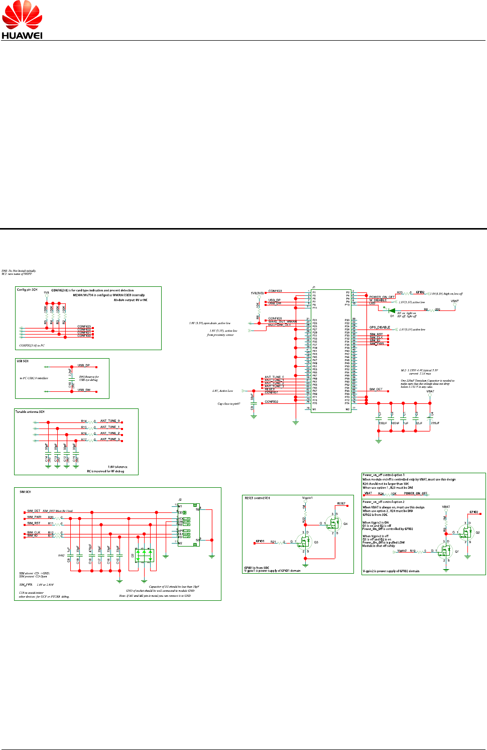
HUAWEI MU736 HSPA+ M.2 Module
ecafretnI lacipyT fo tiucriC A xidneppA ediuG erawdraH
Issue 05 (2014-01-14)
Huawei Proprietary and Confidential
Copyright © Huawei Technologies Co., Ltd. 78
10 Appendix A Circuit of Typical
Interface
HUAWEI MU736 HSPA+ M.2 Module
Hardware Guide
Appendix B Acronyms and Abbreviations
Issue 05 (2014-01-14)
Huawei Proprietary and Confidential
Copyright © Huawei Technologies Co., Ltd.
80
11 Appendix B Acronyms and
Abbreviations
Acronym or Abbreviation
Expansion
AP
Application Process
CCC
China Compulsory Certification
CE
European Conformity
CS
Coding Scheme
CSD
Circuit Switched Data
DC
Direct Current
DMA
Direct Memory Access
DVK
Development Kit
EBU
External Bus Unit
EIA
Electronic Industries Association
EMC
Electromagnetic Compatibility
ESD
Electrostatic Discharge
EU
European Union
FCC
Federal Communications Commission
GMSK
Gaussian Minimum Shift Keying
GPIO
General-purpose I/O
GPRS
General Packet Radio Service
GSM
Global System for Mobile Communication
HBM
Human Body Model
HSIC
High Speed Inter-Chip Interface
HUAWEI MU736 HSPA+ M.2 Module
Hardware Guide
Appendix B Acronyms and Abbreviations
Issue 05 (2014-01-14)
Huawei Proprietary and Confidential
Copyright © Huawei Technologies Co., Ltd.
81
Acronym or Abbreviation
Expansion
HSDPA
High-Speed Downlink Packet Access
HSPA+
Enhanced High Speed Packet Access
HSUPA
High Speed Up-link Packet Access
ISO
International Standards Organization
LCP
Liquid Crystal Polyester
LDO
Low-Dropout
LED
Light-Emitting Diode
M.2
New Name for NGFF
MCP
Multi-chip Package
NGFF
Next Generation Form Factor
NTC
Negative Temperature Coefficient
PA
Power Amplifier
PBCCH
Packet Broadcast Control Channel
PCB
Printed Circuit Board
PDU
Protocol Data Unit
PMU
Power Management Unit
RF
Radio Frequency
RoHS
Restriction of the Use of Certain Hazardous
Substances
TVS
Transient Voltage Suppressor
UMTS
Universal Mobile Telecommunications System
USB
Universal Serial Bus
USIM
Universal Subscriber Identity Module
VSWR
Voltage Standing Wave Ratio
WCDMA
Wideband Code Division Multiple Access
