Hysiry Technology ESP8266-S3 ESP8266-S3 User Manual
Shenzhen Hysiry Technology Co., Ltd. ESP8266-S3
User Manual
Version 1.0
2017 / 9

Shenzhen Hysiry Technology Co.,Ltd T:0755-23596457 2 / 13
Disclaimer and Copyright Notice
Information in this document, including URL references, is subject to change without notice.
THIS DOCUMENT IS PROVIDED AS IS WITH NO WARRANTIES WHATSOEVER, INCLUDING ANYWARRANTY OF
MERCHANTABILITY, NON-INFRINGEMENT, FITNESS FOR ANY PARTICULARPURPOSE, OR ANY WARRANTY
OTHERWISE ARISING OUT OF ANY PROPOSAL, SPECIFICATIONOR SAMPLE. All liability, including liability for
infringement of any proprietary rights, relating to useof information in this document is disclaimed. No licenses
express or implied, by estoppel orotherwise, to any intellectual property rights are granted herein.
The WiFi Alliance Member Logo is a trademark of the WiFi Alliance.
All trade names, trademarks and registered trademarks mentioned in this document are property oftheir
respective owners, and are here by acknowledged.
Note
As the product upgrade or other reasons, this manual may change. Shenzhen Hysiry Technology Co., Ltd has
right to modify the contents of this manual without any notice or warning. This manual is only as a guide,Hysiry
Technology Co., Ltd Spareno effort to provide accurate information in this manual, but the Hysiry can't guarantee
manual there is no problem , all statements in this manual, information and suggestions do not constitute any
guarantee of express or implication.
Amendment record
Time
Version
Specification
2017.09
V1.0
First release

Shenzhen Hysiry Technology Co.,Ltd T:0755-23596457 3 / 13
Contents
1. Overview .......................................................................................................................................................... 4
2. Main Features .................................................................................................................................................. 4
2.1 System Diagram ......................................................................................................................................... 4
2.2 Hardware Specifications ............................................................................................................................ 5
3. Pin description ................................................................................................................................................. 6
4. Functional Description ..................................................................................................................................... 7
4.1 MCU ........................................................................................................................................................... 7
4.2 Memory ..................................................................................................................................................... 7
4.2.1 Internal SRAM and ROM ..................................................................................................................... 7
4.2.2 SPI Flash .............................................................................................................................................. 7
4.3 Interface Description ................................................................................................................................. 8
5. Electrical Characteristic ................................................................................................................................... 9
5.1 Standby Power Consumption .................................................................................................................... 9
5.2 RF Performance ....................................................................................................................................... 10
5.3 Digital Terminal Characteristics ............................................................................................................... 11
5.4 Absolute Maximum Ratings .................................................................................................................... 11
5.5 Reflow Profile .......................................................................................................................................... 11
6. Schematics ..................................................................................................................................................... 12
7. Minimum System Requirements ................................................................................................................... 12
8. Switching noise control ................................................................................................................................. 13
9. Technical Support .......................................................................................................................................... 13
Shenzhen Hysiry Technology Co.,Ltd T:0755-23596457 4 / 13
1. Overview
ESP8266-S3 Wi-Fi module is a low consumption, high performance Wi-Fi network control module designed
by Hysiry. It can meet the IoT application requirements in smart power grids, building automation, security and
protection, smart home, remote health care etc.
The module's core processor ESP8266 integrates an enhanced version of Tensilica's L106 Diamond series 32-
bit processor with smaller package size and 16 bit compact mode, main frequency support 80 MHz and 160 MHz,
support RTOS, integrated Wi-Fi MAC / BB / RF / PA / LNA, on-board PCB antenna.
The module supports standard IEEE802.11 b / g / n protocol, a complete TCP / IP protocol stack.
Users can use the module to add networking capabilities to existing devices, but also to build an independent net
work controller.
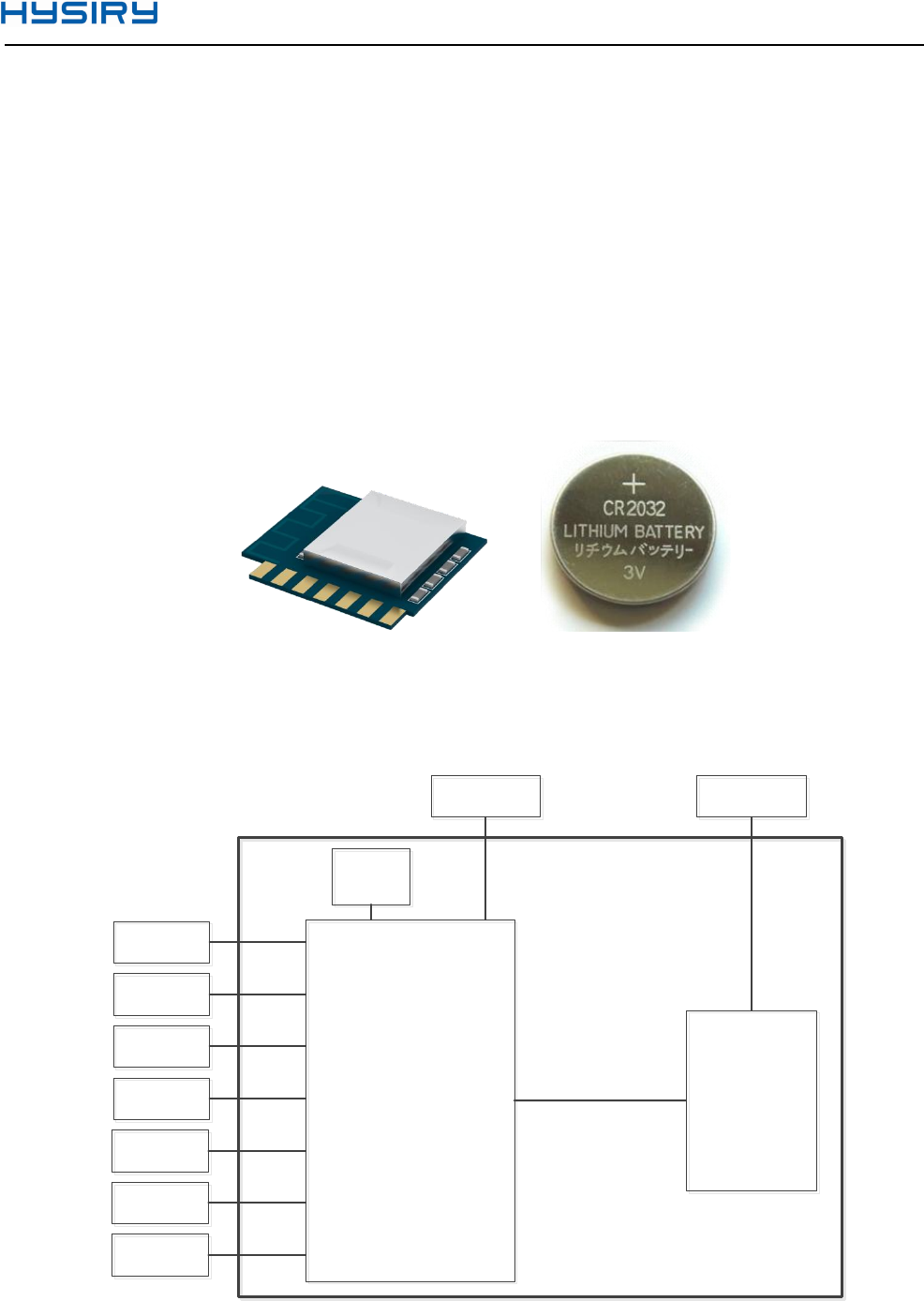
Figure -1.ESP8266-S3 Module
2. Main Features
2.1 System Diagram
ESP8266
ESP8266 8Mbit
SPI FLASH
8Mbit
SPI FLASH
26MHz
XTAL
26MHz
XTAL
VDD_MCU
VDD_MCU VDD33
VDD33
ESP8266-S3
2 Χ UART
2 Χ UART
1 Χ I2S
1 Χ I2S
1 Χ ADC
1 Χ ADC
1 Χ SPI
1 Χ SPI
GPIO
GPIO
1 Χ I2C
1 Χ I2C
1 Χ IR
1 Χ IR
Figure -2. System Diagram

Shenzhen Hysiry Technology Co.,Ltd T:0755-23596457 5 / 13
2.2 Hardware Specifications
Operating Voltage: 3.3V(3.0 ~ 3.6V)
Operating Temperature:-40 - 85°C
CPU Tensilica L106
o RAM 50KB(Available)
o Flash 8 Mbit
System
o 802.11 b/g/n
o Frequency range 2.4 GHz ~ 2.5 GHz(2400 M ~ 2483.5 M)
o IntegratedTensilica L106 ultra-low power 32-bitmicro MCU, with 16-bit RSIC. The CPU clock speed
is 80MHz. It can also reach a maximum value of 160MHz.
o WIFI 2.4 GHz,supportWPA/WPA2
o Supports UART、I2C、GPIO、PWM、SDIO、SPI、ADC、PWM、IR
o Integrated 10 bit high precision ADC
o Supports TCP、UDP、HTTP、FTP
o Integrated TR switch, balun,LNA, Power amplifier and matching network
o Integrated PLL, Regulator and power source management components, +20 dBm output power in
802.11b mode
o Average working current80mA, <Deep sleep current < 20uA, Power down leakage current < 5uA
o Rich interface on processor: SDIO 2.0, SPI, UARTl
o Wake up ,build the connection and transmit packets in < 2ms
o Standby power consumption < 1.0mW (DTIM3)
o Support AT remote upgrades and cloud OTA upgrade
o Support Station / SoftAP / SoftAP+Station operation modes
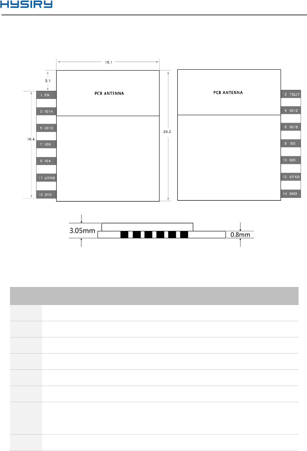
o Ultra-Small 20.2mm * 17.6mm * 3.05mm
Shenzhen Hysiry Technology Co.,Ltd T:0755-23596457 6 / 13
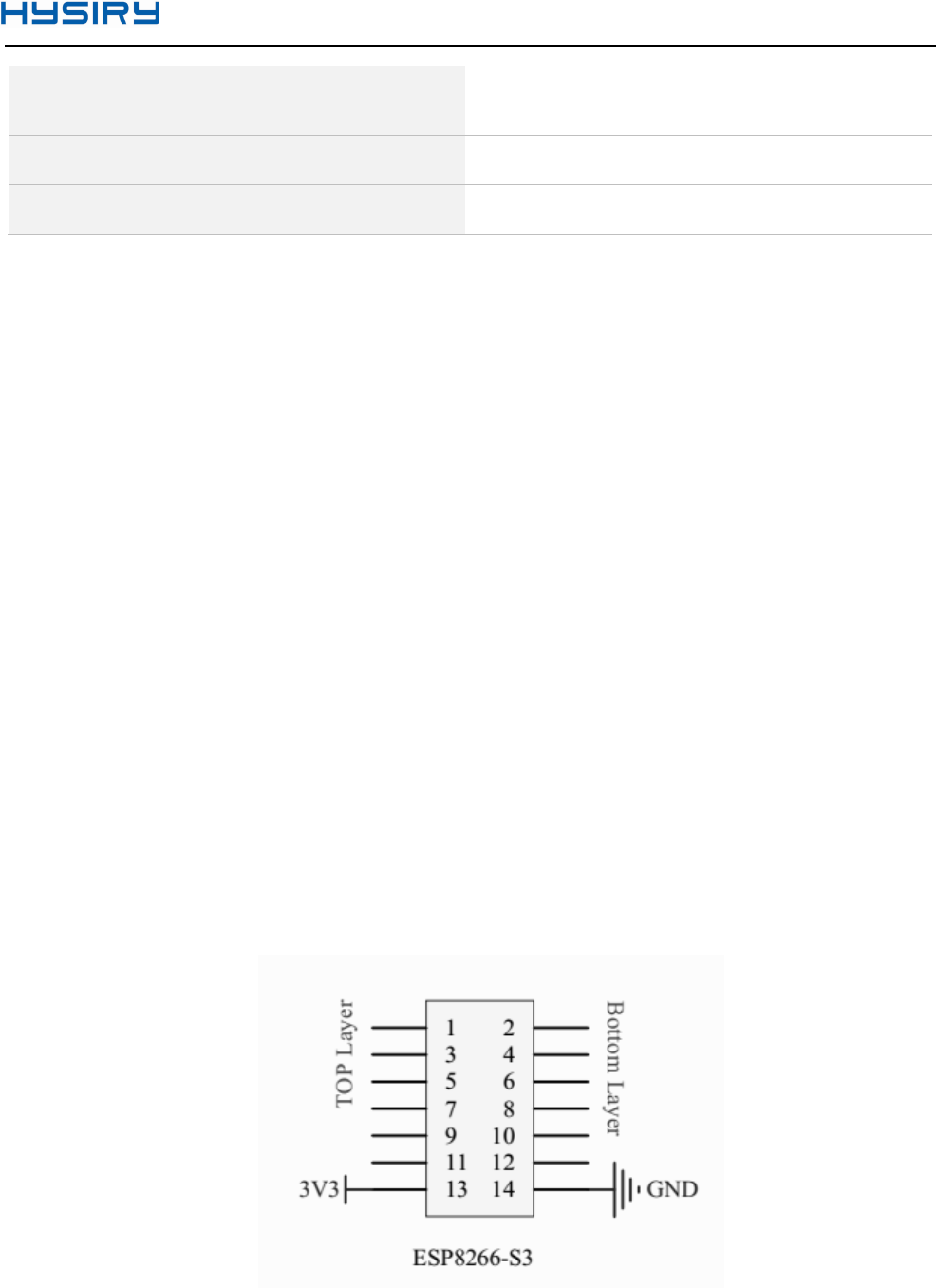
3. Pin description
Figure -3. Pin description
Figure -4.Module Size - shieldingcase (Side View)
Table -1. ESP8266-S3 Pin Definitions
No.
Pin Name
Functional Description
1
EN
Chip enable pin (cannot be floating). Active high.
2
TOUT
Tests the power-supply voltage of VDD3P3 and the input power voltage of
TOUT.These two functions cannot be used simultaneously.
3
IO14
GPIO14;HSPI_CLK
4
IO12
GPIO12;HSPI_MISO
5
IO13
GPIO13; HSPI_MOSI;UART0_CTS
6
IO15
GPIO15;MIDO; HSPICS;UART0_RTS
7
IO0
GPIO0
• UART download: pull down.
• SDIO boot: don’t-care.
8
IO2
GPIO2;UART1_TXD

Shenzhen Hysiry Technology Co.,Ltd T:0755-23596457 7 / 13
9
IO4
GPIO4
10
IO5
GPIO5
11
URXD
UART0_RXD, receive end in UART download;GPIO3
12
UTXD
UART0_TXD, transmit end in UART download, floating (internal pull-up) or
pull up;GPIO1
13
VCC
3.3 V power supply (VDD)
Note:It is recommended the maximum output current a power supply
provides be of 500 mA or above.
14
GND
Ground
4. Functional Description
4.1 MCU
ESP8266EX contained in the ESP8266-S3 integrates Tensilica L106 32-bit micro controller (MCU) and a 16-bit
RSIC. The CPU clock speed is 80 MHz and can reach a maximum value of 160 MHz. The system can readily run a
Real Time Operating System (RTOS). Currently, the Wi-Fi stack only takes up 20% of CPU time. The remaining CPU
time (80% of total MIPS) can be used for user application. The MCU can work in conjunction with the other parts
of the chip through the following interfaces.
Programmable RAM/ROM interface (iBus) that connects to memory controller and can access the
external flash.
Data RAM interface (dBus) that connects to memory controller.
AHB interface that accesses the register.
4.2 Memory
4.2.1 Internal SRAM and ROM
ESP8266EX Wi-Fi SoC integrates memory controller including SRAM and ROM. MCU can access the memory
controller through iBus, dBus, and AHB interfaces. All these interfaces can access ROM or RAM units. A memory
arbiter determines the running sequence in the arrival order of requests.
According to our current version of SDK, SRAM space available to users is assigned as below.
RAM size < 50 kB, that is, when ESP8266EX is working in Station mode and connects to the router,
available space in Heap + Data sector is around 50 kB.
There is no programmable ROM in ESP8266EX, therefore, user program must be stored in the SPI flash
integrated into the ESP8266-S3.
4.2.2 SPI Flash
ESP8266EX supports SPI flash. Theoretically speaking, ESP8266EX can support up to 16 MB SPI flash.
ESP8266-S3 currently integrates 8 Mbit SPI flash memory. ESP8266-S3 supports these SPI modes:

Shenzhen Hysiry Technology Co.,Ltd T:0755-23596457 8 / 13
Standard SPI, DIO (Dual I/O), DOUT (Dual Output), QIO (Quad I/O) and QOUT (Quad Output).
4.3 Interface Description
Table -2. Interface Description
Interface
Pin
Functional Description
SPI
IO12(MISO),IO13(MOSI),
IO14(CLK),IO15(CS)
S3 can control SPI Slave as a Master or communicate with
Host MCU as a Slave. In overlap mode, S3 can share the SPI
interface with Flash, shifted by different CS signals.
PWM
Any available GPIO
(EXCEPT GPIO16)
Currently the demo provides 4 PWM channels (users can
extend to 6 channels). PWM interface can realize the control
of LED lights, buzzers, relays, electronic machines, etc.
IR
Any available GPIO
(EXCEPT GPIO16)
The functionality of Infrared remote control interface can be
implemented via software programming. NEC coding,
modulation, and demodulation are used by this interface. The
frequency of modulated carrier signal is 38KHz.
ADC
TOUT
ESP8266EX integratesa 10-bit precision SARADC.
ADC_IN interface is used to test the power supply voltage of
VDD3P3(Pin 3 and Pin 4), as well as the input voltage of TOUT
(Pin 6). It can be used in sensors application.
I2C
IO14(SCL), IO2(SDA)
Any available
GPIO(EXCEPT GPIO16)
Can connect to external sensor and display, etc.
UART
UART0:
TXD(U0TXD),RXD(U0RXD)
,IO15(RTS),IO13(CTS)
Devices with UART interfaces can be connected
Download:U0TXD+U0RXD or GPIO2+U0RXD
Communication:
(UART0):U0TXD,U0RXD,MTDO(U0RTS),MTCK(U0CTS)
Debug:UART1_TXD(GPIO2)Can be used to print debugging
information
UART1: IO2(TXD)
By default, UART0 will output some printed information when
the device is powered on and is booting up. If this issue exerts
influence on some specific applications, users can exchange
the inner pins of UART when initializing, that is to say,
exchange U0TXD, U0RXD with U0RTS, U0CTS.
I2S
I2S input:
IO12 (I2SI_DATA);
IO13 (I2SI_BCK );
IO14 (I2SI_WS);
Mainly used for audio capturing, processing and transmission
I2S output:
IO15 (I2SO_BCK );
IO3 (I2SO_DATA);
IO2 (I2SO_WS );
Shenzhen Hysiry Technology Co.,Ltd T:0755-23596457 9 / 13
5. Electrical Characteristic
5.1 Standby Power Consumption
Table -3. Standby Power Consumption
Mode
Status
Typical Value
Standby
Modem Sleep
15mA
Light Sleep
0.9mA
Deep Sleep
20uA
Off
0.5uA
Working(Average)
80mA
Tx 801.11b,CCK 11Mbps,P OUT=+17 dBm
170mA
Tx 801.11g,OFDM 54Mbps,P OUT =+15 dBm
140mA
Tx 801.11n,MCS7,P OUT =+13 dBm
120mA
Rx 801.11b,1024 bytes packet length,-80 dBm
50mA
Rx 801.11g,1024 bytes packet length,-70 dBm
56mA
Rx 801.11n,1024 bytes packet length,-65 dBm
56mA
The following current consumption is based on 3.3V supply and 25°C ambient with internalregulators.Values
are measured at antenna port without SAW filter. All the transmissionmeasurements valuesare based on 90%
duty cycle, continuous transmission mode.
Table -4.Standby Power Consumption
Mode
Status
Typical Value
Standby
Modem Sleep
15mA
Light Sleep
0.9mA
Deep Sleep
20uA
Off
0.5uA
Power Save Mode
(2.4G)
(Low Power Listen
disabled) ¹
DTIM period
Current Cons. (mA)
T1 (ms)
T2 (ms)
Tbeacon (ms)
T3
(ms)
DTIM 1
1.2
2.01
0.36
0.99
0.39
DTIM 3
0.9
1.99
0.32
1.06
0.41
①: Modem-Sleep requires the CPU to be working, as in PWM or I2S applications. According to802.11
standards (like U-APSD), it saves power to shut down the Wi-Fi Modem circuit whilemaintaining a Wi-Fi

Shenzhen Hysiry Technology Co.,Ltd T:0755-23596457 10 / 13
connection with no data transmission. E.g. in DTIM3, to maintain a sleep 300mswake 3ms cycle to receive AP’s
Beacon packages, the current is about 15mA.
②: During Light-Sleep, the CPU may be suspended in applications like Wi-Fi switch. Without
datatransmission, the Wi-Fi Modem circuit can be turned off and CPU suspended to save poweraccording to the
802.11 standard (U-APSD). E.g. in DTIM3, to maintain a sleep 300ms-wake 3mscycle to receive AP’s Beacon
packages, the current is about 0.9mA.
③: Deep-Sleep does not require Wi-Fi connection to be maintained. For application with long timelags
between data transmission, e.g. a temperature sensor that checks the temperature every 100s,sleep 300s and
waking up to connect to the AP (taking about 0.3~1s), the overall average current isless than 1mA.
5.2 RF Performance
Table -5. RF Performance
Description
Min
Typ
Max
Unit
Input frequency
2400
/
2483.5
MHz
Input impedance
/
50
/
ohm
Input reflection
/
/
-10
dB
PA output power at 72.2
Mbps
15.5
16.5
17.5
dBm
PA output power in 11b
mode
19.5
20.5
21.5
dBm
Sensitivity
CCK,1Mbps
/
-98
/
dBm
CCK,11Mbps
/
-91
/
dBm
6Mbps(1/2 BPSK)
/
-93
/
dBm
54Mbps(3/4 64-QAM)
/
-75
/
dBm
HT20,MCS7(65Mbps,
72.2Mbps)
/
-72
/
dBm
Adjacent channel rejection
OFDM,6Mbps
/
37
/
dB
OFDM,54Mbps
/
21
/
dB
HT20,MCS0
/
37
/
dB
HT20,MCS7
/
20
/
dB
Shenzhen Hysiry Technology Co.,Ltd T:0755-23596457 11 / 13
5.3 Digital Terminal Characteristics
Table -6. Digital Terminal Characteristics
Terminals
Symbol
Min
Max
Unit
Input logic level low
VIL
-0.3
0.25 VDD
V
Input logic level high
VIH
0.75 VDD
VDD + 0.3
V
Output logic level low
VOL
N
0.1 VDD
V
Output logic level high
VOL
0.8 VDD
N
V
5.4 Absolute Maximum Ratings
Table -7. Absolute Maximum Ratings
Rating
Condition
Value
Unit
Storage temperatue
/
-40 to 125
°C
Maximum soldering
temperature
/
260
°C
Supply voltage
IPC/JEDEC J-STD-020
+3.0 to +3.6
V
5.5 Reflow Profile
Table -8. Reflow Profile
Indicator
Value
Ramp-up Rate (TS Max to TL)
3 °C /second max.
Prehea
Temperature Min. (TS Min.)
Temperature Typ. (TS Typ.)
Temperature Min. (TS Max.)
Time (TS)
150°C
175°C
200°C
60 ~ 180 seconds
Ramp-up Rate (TL to TP)
3°C /second max
Time maintained above: Temperature
(TL)/Time (TL)
270°C / 60 ~ 150 seconds
Peak temperature (TP)
260 °C max, for 10 seconds
Target Peak Temperature (TP Target)
260 °C + 0 / -5°C
Shenzhen Hysiry Technology Co.,Ltd T:0755-23596457 12 / 13
Time within 5°C of actual Peak Temperature
(TP)
20 ~ 40 seconds
TS max to TL (Ramp-down Rate)
6°C / second max.
Time 25°C to Peak Temperature (t)
8 minutes max.
6. Minimum System Requirements
Figure -6. ESP8266-S3 minimum system

Shenzhen Hysiry Technology Co.,Ltd T:0755-23596457 13 / 13
7. Switching noise control
ESP8266-S3 has high speed GPIO and peripheral interfaces which can create severe switching noise. In
applications where power consumption and EMI profile are important, it is recommended that a series resistor of
10-100 ohms be placed with digital I/O. This limits overshoot during switching and results in smoother transitions.
A series resistor may also protect from ESD to some extents.
8. Technical Support
E-mail:technical@hysiry.com
FCC Caution: Any changes or modifications not expressly
approved by the party responsible for compliance could void the user's authority to operate this equipment.
This device complies with Part 15 of the FCC Rules.
Operation is subject to the following two conditions: (1) This device may not cause harmful interference, and
(2) this device must accept any interference received, including interference that may cause undesired operation. This
device and its antenna(s) must not be co-located or operating in conjunction with any other antenna or transmitter.
15.105 Information to the user.
(b) For a Class B digital device or peripheral, the instructions furnished the user shall include the following or
similar statement, placed in a prominent location in the text of the manual:
Note: This equipment has been tested and found to comply
with the limits for a Class B digital device, pursuant to part 15 of the FCC Rules.
These limits are designed to provide reasonable protection against harmful
interference in a residential installation. This equipment generates, uses and
can radiate radio frequency energy and, if not installed and used in
accordance with the instructions, may cause harmful interference to radio
communications. However, there is no guarantee that interference will not
occur in a particular installation. If this equipment does cause harmful
interference to radio or television reception, which can be determined by
turning the equipment off and on, the user is encouraged to try to correct the
interference by one or more of the following measures:
—Reorient or relocate the receiving antenna.
—Increase the separation between the equipment and receiver.
—Connect the equipment into an outlet on a circuit different from that to which the receiver is connected.
—Consult the dealer or an experienced radio/TV technician for help.
The availability of some specific channels and/or operational frequency bands are country dependent and
are firmware programmed at the factory to match the intended destination.
The firmware setting is not accessible by the end user.
The final end product must be labelled in a visible area with the following:
Contains Transmitter Module FCC ID:2AKBPESP8266-S3. .
FCCRadiationExposureStatement:
ThisequipmentcomplieswithFCCradiationexposurelimitssetforthforanuncontrolledenvironment.
Thisequipmentshouldbeinstalledandoperatedwithminimumdistance20cmbetweentheradiator&
yourbody.
OEMINTEGRATIONINSTRUCTIONS:
ThisdeviceisintendedonlyforOEMintegratorsunderthefollowingconditions:
Themodulemustbeinstalledinthehostequipmentsuchthat20cmismaintainedbetweenthe
antennaandusers,andthetransmittermodulemaynotbeco‐locatedwithanyothertransmitteror
antenna.Themoduleshallbeonlyusedwiththeinternalon‐boardantennathathasbeenoriginally
testedandcertifiedwiththismodule.Externalantennasarenotsupported.Aslongasthese3
conditionsabovearemet,furthertransmittertestwillnotberequired.
However,theOEMintegratorisstillresponsiblefortestingtheirend‐productforanyadditional
compliancerequirementsrequiredwiththismoduleinstalled(forexample,digitaldeviceemissions,PC
peripheralrequirements,etc.).Theend‐productmayneedVerificationtesting,Declarationof
Conformitytesting,aPermissiveClassIIChangeornewCertification.PleaseinvolveaFCCcertification
specialistinordertodeterminewhatwillbeexactlyapplicablefortheend‐product.