IP Mobilenet ECSHPA80TX RF Amplifier User Manual USERS MANUAL
IP Mobilenet, LLC RF Amplifier USERS MANUAL
UserManual.wiki
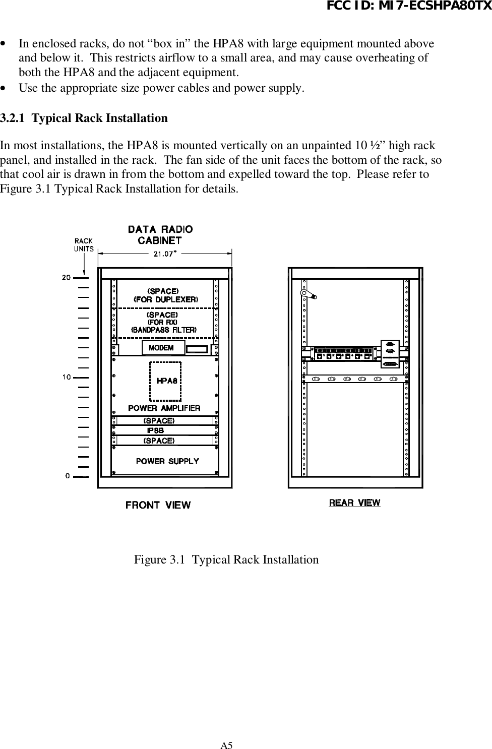
>
IP Mobilenet
>
ECSHPA80TX User Manual
USERS MANUAL
Navigation menu
Upload a User Manual
Namespaces
Wiki Guide
HTML
PDF
Info
Views
User Manual
Discussion / Help
Navigation