IP Mobilenet ECSHPA80TX RF Amplifier User Manual USERS MANUAL
IP Mobilenet, LLC RF Amplifier USERS MANUAL
USERS MANUAL
FCC ID: MI7-ECSHPA80TX
A1
A
Ap
pp
pe
en
nd
di
ix
x
A
A

FCC ID: MI7-ECSHPA80TX
A2
E
EL
LE
EC
CT
TR
RO
OC
CO
OM
M
I
IN
NV
VA
AD
DR
Rt
tm
m
M
MO
OB
BI
IL
LE
E
D
DA
AT
TA
A
A
AN
ND
D
V
VO
OI
IC
CE
E
S
SY
YS
ST
TE
EM
M
C
CO
OM
MP
PO
ON
NE
EN
NT
T
HPA8
800 MHZ HIGH POWER AMPLIFIER
PRODUCT SUPPORT MANUAL
Document Number 516-80075
Revision X2
11909 East Telegraph Road, Santa Fe Springs, CA 90670-3785
Voice: (562) 946-9493 Fax: (562) 949-0223
FCC ID: MI7-ECSHPA80TX
Ai
NOTICES
INVADRtm is a registered trademark of ElectroCom Systems, Inc.
Contents copyrighted 2001 by ElectroCom Systems, Inc. All rights reserved.
FCC ID: MI7-ECSHPA80TX
Aii
CONTENTS
1. Introduction .................................................................................... 1
1.1 Scope ...................................................................................... 1
1.2 Reference Materials ................................................................ 2
1.2.1 ElectroCom Documents ............................................... 2
1.3 Product Description ................................................................ 3
1.4 Product Features ..................................................................... 3
2. Interface Description ..................................................................... 4
3. Installation ..................................................................................... 4
3.1 Unpacking ............................................................................... 4
3.2 Installation .............................................................................. 5
3.2.1 Typical Rack Installation .............................................. 5
3.2.2 Installation Instructions ................................................ 5
4. Theory of Operation ...................................................................... 6
4.1 Thermal Equilibration System ............................................... 6
4.2 RF Amplifier Section ............................................................. 7
5. Maintenance .................................................................................. 9
6. Specifications ................................................................................ 9
7. Warranty and Service .................................................................... 10
7.1 Warranty ................................................................................. 10
7.2 Warranty/Non-Warranty Service ............................................ 10
8. Diagrams and Lists ........................................................................ 11
8.1 Block Diagram
8.2 Schematic Diagram
8.3 Interconnection Diagram
8.4 Board Parts List
FCC ID: MI7-ECSHPA80TX
A1
1. Introduction
1.1 Scope
This document describes the hardware of the HPA8 High Power Amplifier as follows:
Section 1: Overview of the unit and its features.
Section 2: Interfaces (e.g. connectors, power sources, etc.).
Section 3: Installation procedure.
Section 4: Circuit theory.
Section 5: Maintenance procedures.
Section 6: Specifications.
Section 7: Warranty and warranty/non-warranty service information.
Section 8: Diagrams and lists.

FCC ID: MI7-ECSHPA80TX
A2
1.2 Reference Materials
1.2.1 ElectroCom Documents (attached)
The following ElectroCom documents are provided as attachments to Section 8:
NUMBER DOCUMENT NO. DESCRIPTION
1HPA8 Block Diagram
2 502-80228 Interconnection Diagram
3 502-80228 Schematic Diagram
4 502-80292 PWA Parts List
FCC ID: MI7-ECSHPA80TX
A3
1.3 Product Description
The ElectroCom HPA8 High Power Amplifier was designed specifically to operate with
the ElectroCom IP8B Base Station Data Transceiver. Basically, the unit amplifies the RF
output of the IP8B, providing up to 80 watts of RF power for the antenna system. The
HPA8 is intended for base station use only.
For enhanced reliability, the HPA8 incorporates a four power amplifier module design
which permits “graceful” degradation of output power under fault conditions. This
means the unit will continue to operate (albeit at gradually reduced power levels) despite
failures in up to three power amplifier modules.
The useful life of the HPA8 is extended by a 3-stage thermal “equilibration” scheme.
“Equilibration” refers to the act of equalizing the operating temperatures of the four
power amplifier modules. By doing so, and by keeping the temperature within
reasonable limits, heat stress on the modules is minimized. This results in longer
operating life for the modules, and increased overall reliability for the HPA8.
The HPA8 is equipped with over-temperature and over-voltage protection. To prevent
damage from excessive heat, or from a defective power supply, the cabinet temperature
and power supply voltage is monitored at all times.
1.4 Product Features
The HPA8 High Power Amplifier features:
• 80 watts RF output (typical).
• Covers 851-866 MHz
• Four power amplifier module design.
• Graceful degradation of power under fault conditions.
• 3-stage thermal equilibration protection system.
• Over-temperature protection.
• Over-voltage protection.
• 13.8 VDC operation.
• Compact size, rugged construction.
FCC ID: MI7-ECSHPA80TX
A4
2. Interface Description
As shown in section 8.3, the HPA8 has the following interface connections:
J1 RF input. Typically connects to the IP8B Base Station Data Transceiver.
J2 RF output. Typically connects to the antenna system components in the rack.
WARNING! Do not remove the harmonic filter, or operate the HPA8 without the
filter installed. Excessive harmonic emissions may result.
J3 DC power connector. Plugs into a 13.8 volt (nominal), 25 amp (or greater) DC
power supply.
J4 Control interface connector. The transmit keying input connects to the IP8B
Base Station Data Transceiver via an INVADR I/O Interface Board mounted
on the rack. The high temperature alarm output may be connected to an alarm
monitoring system, or to the ALARM connector on the INVADR I/O Interface
Board.
3. Installation
3.1 Unpacking
Upon opening the carton, carefully inspect the amplifier for any signs of shipping
damage. If there is evidence of damage, file a claim immediately with the carrier and
contact your dealer. Keep the original shipping container for verification of damage after
filing the claim.
3.2 Installation
When planning an HPA8 High Power Amplifier installation, be sure to consider the
amount of air flow available in the amplifier’s mounting location. Also make sure that
adequate space exists for the routing of the RF, power, and control cables.
Note: RF, power, and control cables should be provided with service loops. This makes
it easier to remove and install the unit in the future.
For long life, be sure to observe the following installation precautions:
• Allow at least 3” clearance at each end of the heatsink for good airflow.
• Install the unit with the fan side closest to the bottom of the rack.
• Do not allow cables or other components to obstruct the airflow.
FCC ID: MI7-ECSHPA80TX
A5
• In enclosed racks, do not “box in” the HPA8 with large equipment mounted above
and below it. This restricts airflow to a small area, and may cause overheating of
both the HPA8 and the adjacent equipment.
• Use the appropriate size power cables and power supply.
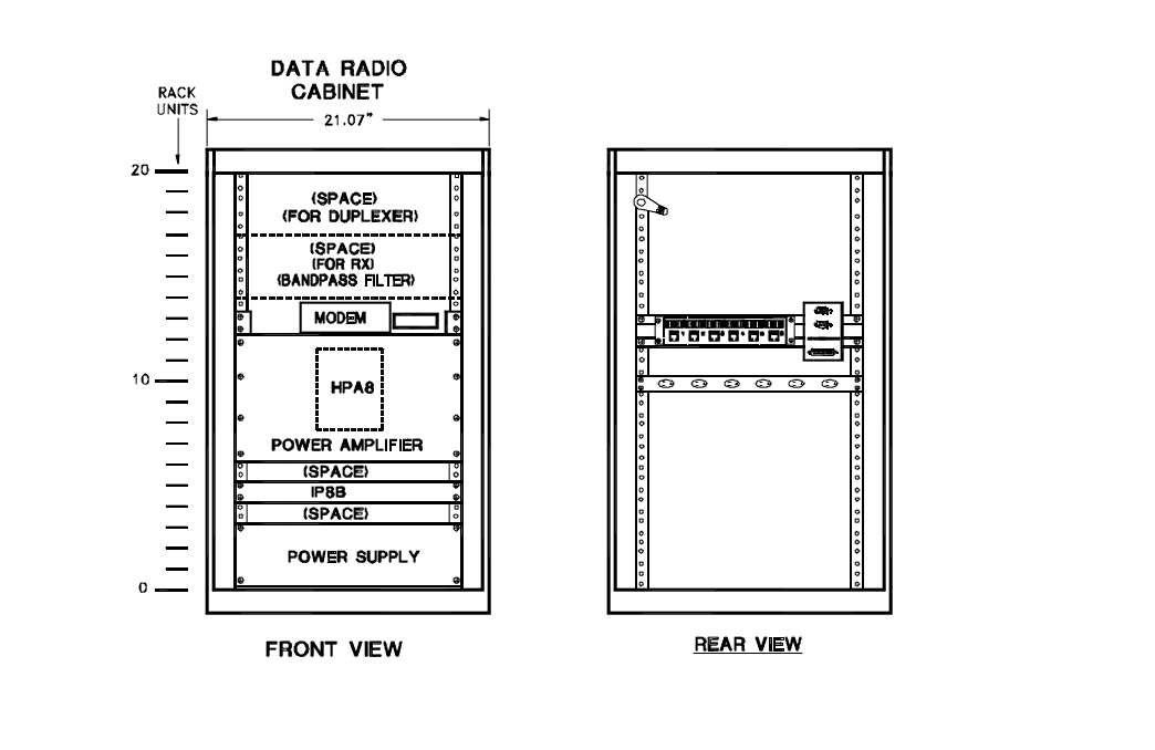
3.2.1 Typical Rack Installation
In most installations, the HPA8 is mounted vertically on an unpainted 10 ½” high rack
panel, and installed in the rack. The fan side of the unit faces the bottom of the rack, so
that cool air is drawn in from the bottom and expelled toward the top. Please refer to
Figure 3.1 Typical Rack Installation for details.
Figure 3.1 Typical Rack Installation
FCC ID: MI7-ECSHPA80TX
A6
3.2.2 Installation Instructions
Install the HPA8 High Power Amplifier as follows:
1. Unpack the unit.
2. Mount the HPA8 on the rack panel (supplied). To do this, center the unit over the six
mounting holes in the panel and attach with the supplied hardware.
3. Install the HPA8 panel assembly in the rack. Position it so the fan is facing down, and
so that the HPA8 unit goes inside the rack. Secure the assembly to the rack with the
appropriate screws and cup washers.
4. Connect a coax jumper cable to the TX output of the IP8B Base Station Data Trans-
ceiver. Connect the other end to J1 (RF input) on the HPA8.
5. Connect a coax jumper cable to J2 (RF output with harmonic filter) on the HPA8.
Connect the other end to the transmitter IM suppression panel, or other RF device, as
appropriate.
WARNING! Do not remove the harmonic filter from J2, or operate the HPA8 without
the filter installed. Excessive harmonic emissions may result.
6. Connect the power cable to J3 (power). Attach the other end to the DC power supply
terminals. Black goes to the minus terminal. Red goes to the plus terminal.
7. Connect J4 (control interface). The transmit keying input goes to pin 1 of the PA
connector on the INVADR I/O Interface Board. This board is typically mounted on the
back of the rack, and it plugs into the IP8B Base Station Data Transceiver. Optionally,
the high temperature alarm output of J4 may be connected to an external alarm moni-
toring device, or to the ALARM connector on the INVADR I/O Interface Board.
8. The HPA8 is installed and ready for use.
FCC ID: MI7-ECSHPA80TX
A7
4. Theory of Operation
4.1 Thermal Equilibration System
“Equilibration” refers to the act of equalizing the operating temperatures of the four
power amplifier modules. By doing so, and by keeping the temperature within reason-
able limits, heat stress on the modules is reduced. This results in longer operating life for
the modules, and increased overall reliability for the HPA8.
Thermal equilibration is accomplished by: 1) attaching the power amplifier modules to a
thick aluminum substrate (heatsink) with heat conducting grease; 2) bonding over-sized
heat radiating fins into the substrate for greater heat transfer; 3) providing a thermo-
statically controlled fan which keeps the heatsink temperature within limits.
4.2 RF Amplifier Section
The HPA8 High Power Amplifier incorporates all circuitry on a single printed circuit
board. Please refer to the schematic diagrams in Section 8 for details while reading about
the circuitry.
Sheet 1 of 6. Block diagram. This sheet illustrates five functional circuit blocks in the
unit. Sheet 2, Pwr and Gnd, provides regulated power for the logic and fan control
circuitry. Sheet 3 contains transmit keying, over-temperature protection, and over-
voltage protection circuitry. Sheet 4 offers the RF input, driver, and power divider
circuitry. Sheet 5, Pwr Amp Modules, and Sheet 6, Pwr Combiner, are self-explanatory.
Sheet 2 of 6. Voltage regulators and fan control circuitry. Regulator VR1 provides a 5
volt DC output for all logic circuitry on the board. Regulator VR2 provides an 8 volt DC
output for the 1 watt driver amplifier on sheet 4.
The large fan mounted on the heatsink is controlled by the remaining circuitry. When the
cabinet temperature exceeds approximately 110o F, temperature sensor U1 makes the
OUT pin low. This turns on FET Q1, which applies power to the fan via the FP output.
The temperature setpoint is determined by resistor R2.
FCC ID: MI7-ECSHPA80TX
A8
Sheet 3 of 6. Transmit keying, over-temperature, and over-voltage protection circuitry.
The transmit keying circuitry is shown at the top of the page. To transmit, the IP8B Base
Station Data Transceiver grounds the KEY input. This input is gated with the normally
high over-temperature and over-voltage inputs to produce a logic low (0V) on the output
of gate U2D. This turns off transistor Q7, applying base current to transistors Q8, Q6,
and Q10. As a result, transistor Q8 turns on FETs Q4 and Q5, applying 13.6 volts DC to
the four power amplifier modules. FET Q4 powers two modules, while FET Q5 powers
the other two modules. At the same time, transistor Q6 turns on FET Q2, applying 5
volts to the 1 watt driver circuit. This makes it active. And finally, transistor Q10 turns
on FET Q9, applying power to adjustable voltage regulator U5. Regulator U5 develops a
low voltage DC source which biases the four power amplifier modules for Class AB
operation.
The over-temperature circuitry consists of temperature sensor U3 and transistor Q3. A
temperature setpoint of approximately 150o F is determined by resistor R22. In
operation, the OUT terminal of sensor U3 is normally logic high. This permits normal
operation of the HPA8 via gate U2B. Transistor Q3 is also turned on, producing a low on
the HTA (High Temperature Alarm) output. Should the cabinet temperature exceed the
150o F setpoint, the OUT terminal on U3 goes low. This shuts down the HPA8 via gate
U2B and turns off transistor Q3. As a result, the HTA output goes high. If an external
alarm monitoring device is connected to the HTA output, it will warn users there is a
fault with the HPA8. When the cabinet temperature cools slightly below the setpoint, the
OUT terminal goes high, and normal operation resumes.
The over-voltage circuitry consists of reference diode CR1 and op amp U4A. The 16.0
volt threshold is set by resistors R16/R21, and the 2.5 volt output of reference CR1. In
operation, U4A monitors the 2.5 volt reference and the divided-down power input
voltage. When the voltage at the junction of R16 and R21 exceeds 2.5 volts, the U4A
output goes low, turning on OVER VOLTAGE LED D2, and turning off the unit via gate
U2D. This condition occurs when the DC power input is approximately 16.0V. When
the voltage drops to less than 15.75 volts, the U4A output goes high, LED D2 turns off,
and the unit resumes operation. The 15.75 volt drop-out voltage is set by resistor R14.
FCC ID: MI7-ECSHPA80TX
A9
Sheet 4 of 6. RF input, driver, and power divider circuitry. The purpose of this circuitry
is to attenuate the incoming RF energy, amplify it to a useful level, and to divide it into
four equal parts for the power amplifier modules. This design approach allows the HPA8
to accept a wider range of RF power levels than otherwise possible.
The RF input circuitry is built around coupler DC1 and adjustable attenuator AT1. In
operation, RF energy from the IP8B Base Station Data Transceiver appears at the RF IN
pad. Coupler DC1 reduces the RF signal level by 75%, courtesy of resistors R26 and
R30. The RF is sent to the attenuator via capacitor C16. DC controlled attenuator AT1
adjusts the RF power level for the desired output (typically 80 watts). Pot R25 controls
the attenuator. Capacitor C17 couples the RF output to the driver circuitry.
The driver circuitry consists of amplifier U6. This device boosts the RF signal from
attenuator AT1 to up to one watt of RF power. Amplifier U6 is operated by a 8 volt
regulated source and a DC control input from sheet 3. To transmit, the 5VKEY input is
made high and amplifier U6 becomes active. This produces an RF output on pin 13.
From there the RF goes through a PI filter consisting of capacitors C20/C21 and choke
L1. The filter provides harmonic suppression and impedance transformation for the
couplers in the power divider section. Chokes L2 and L3 provide a DC path for the
circuitry inside of U6, while capacitor C22 blocks DC from the RF before it goes to the
power dividers.
The power divider circuitry consists of three hybrid couplers. The purpose of these
devices is to divide the RF power output into four equal parts. Coupler HC3 accepts RF
from the driver, and it produces outputs at 0o and –90o. Coupler HC1 is driven by the 0o
port of HC3. It produces RF outputs at 0o and –90o for the first two power amplifier
modules. Coupler HC2 is driven by the -90o port of HC3. It produces RF outputs at -90o
and –180o for the second pair of power amplifier modules.
Sheet 5 of 6. Power amplifier modules. The four hybrid power amplifier modules are
shown here. The devices are powered through FET switches on sheet 3 via VS1 and
VS2. The four modules are biased for class AB operation via VBB. This voltage is
developed by an adjustable voltage regulator on sheet 3.
Should a power amplifier module fail, a portion of the power is lost. As a result, the
power output drops from 80 watts to 60 watts. Should a second power amplifier module
fail, the power output drops from 80 watts to 40 watts for the same reason. This is the
“graceful degradation of power under fault conditions” concept in operation.

FCC ID: MI7-ECSHPA80TX
A10
Sheet 6 of 6. Power combiner section. Three hybrid couplers are shown here. The
purpose of these devices is to combine the RF outputs from the power amplifier modules
in phase.
Capacitor C23 and transmission line TRL1 form a tuned stub which reduces harmonic
emissions. An isolator protects the power amplifiers from damage if a high VSWR load
is connected. An external harmonic filter (not shown) attached to the RF OUT connector
provides an additional measure of harmonic suppression.
5. Maintenance
The HPA8 High Power Amplifier has modest maintenance requirements. However, for
long, trouble free life, it is important to assure good, unobstructed airflow through the
unit. Keep the following maintenance items in mind when working with the unit.
• Periodically inspect the heatsink and fan grille for dust build-up. Clean with a soft
brush and a vacuum cleaner when necessary.
• Inspect the connectors and verify they are tight.
6. Specifications
Published specifications for the HPA8 High Power Amplifier:
PARAMETER SPECIFICATION
Frequency Range 851 - 866 MHz
Output Power 80W minimum, 851-866 MHz
Duty Cycle 100%
Power Gain 29 dB nominal
Power Supply
Voltage 13.8 VDC nominal (16 VDC maximum)
Power Supply 0A standby
Current 20A transmit at 80W output
RF Input Power 100 mW nominal
RF Connectors Two type “N” female jacks (RF in/RF out)
Load Mismatch
Tolerance Infinite
Temp. Range,
Operating -30oC to +60oC (-22oF to +140oF)
Size 7.0” H x 7.38” W x 11.0” D (incl. J1, J2)
Weight 11.5 lbs
Emission Designator F1D
FCC ID: MI7-ECSHPA80TX
A11
7. Warranty and Service
7.1 Warranty
The HPA8 High Power Amplifier is covered by a one year parts and workmanship war-
ranty. The warranty goes into effect upon shipment.
The warranty does not cover Acts of God such as damage from a lightning strike, fire, or
a flood. The warranty does not cover damage arising from user tampering or user mis-
adjustment.
The customer is responsible for isolating the fault to the HPA8, and for removing and
reinstalling the unit for service. Please note that equipment found to be in good working
order upon receipt at the factory may be subject to a service charge.
Service for units not under warranty is available on a time-and-materials basis from the
ElectroCom factory.
7.2 Warranty/Non-warranty Service
To obtain factory service for the HPA8, perform the following:
1. Contact the following person and request a Return Authorization (RA) Number.
Anita Chavez,
Administration
ElectroCom Systems, Inc.
11909 E. Telegraph Rd.
Santa Fe Springs, CA 90670
(562) 946-9493
You will be faxed a document containing the RA Number and other information on the
unit.
2. Ship the unit to the address indicated on the faxed document.
Important! Do not forget to print the RA Number on the label. Be sure to enclose the
faxed document with the unit.
FCC ID: MI7-ECSHPA80TX
A12
8. Diagrams and Lists
Please refer to the HPA8 Block Diagram, Schematic Diagrams, Interconnection Diagram,
and Parts Lists on the following pages.