IP Mobilenet F32700N25 700/800 MHz 32k Fixed Radio User Manual
IP Mobilenet, LLC 700/800 MHz 32k Fixed Radio Users Manual
UserManual.wiki
>
IP Mobilenet
>
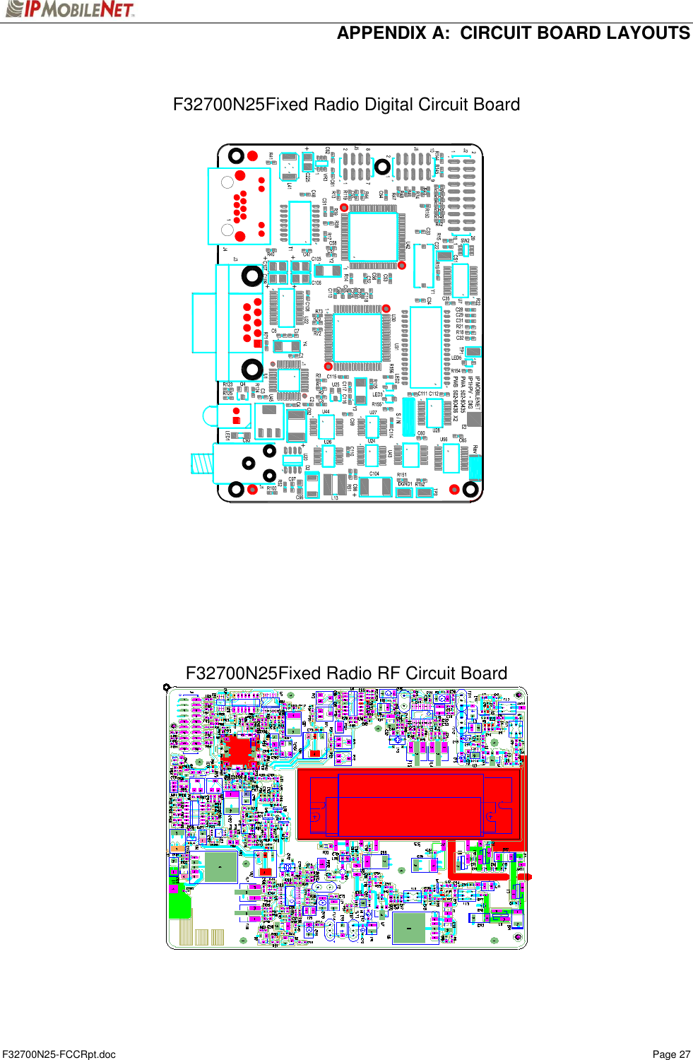
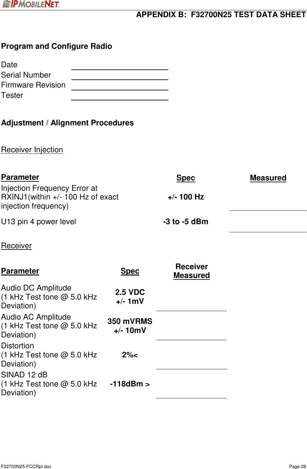
F32700N25 User Manual
Users Manual
Navigation menu
Upload a User Manual
Namespaces
Wiki Guide
HTML
PDF
Info
Views
User Manual
Discussion / Help
Navigation
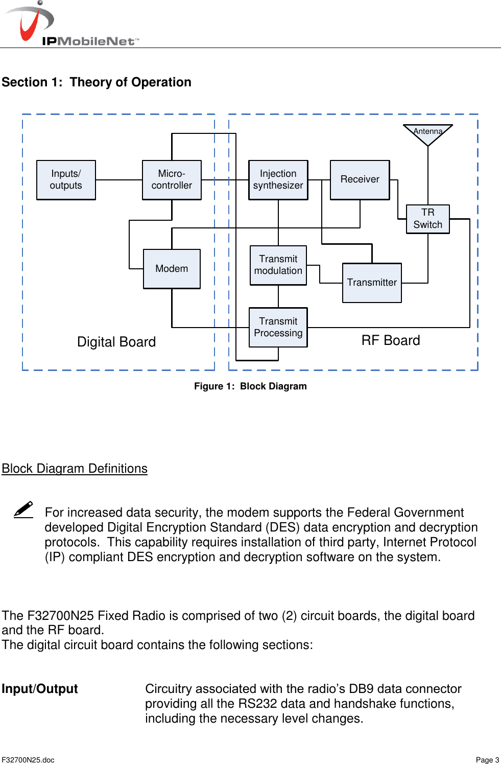
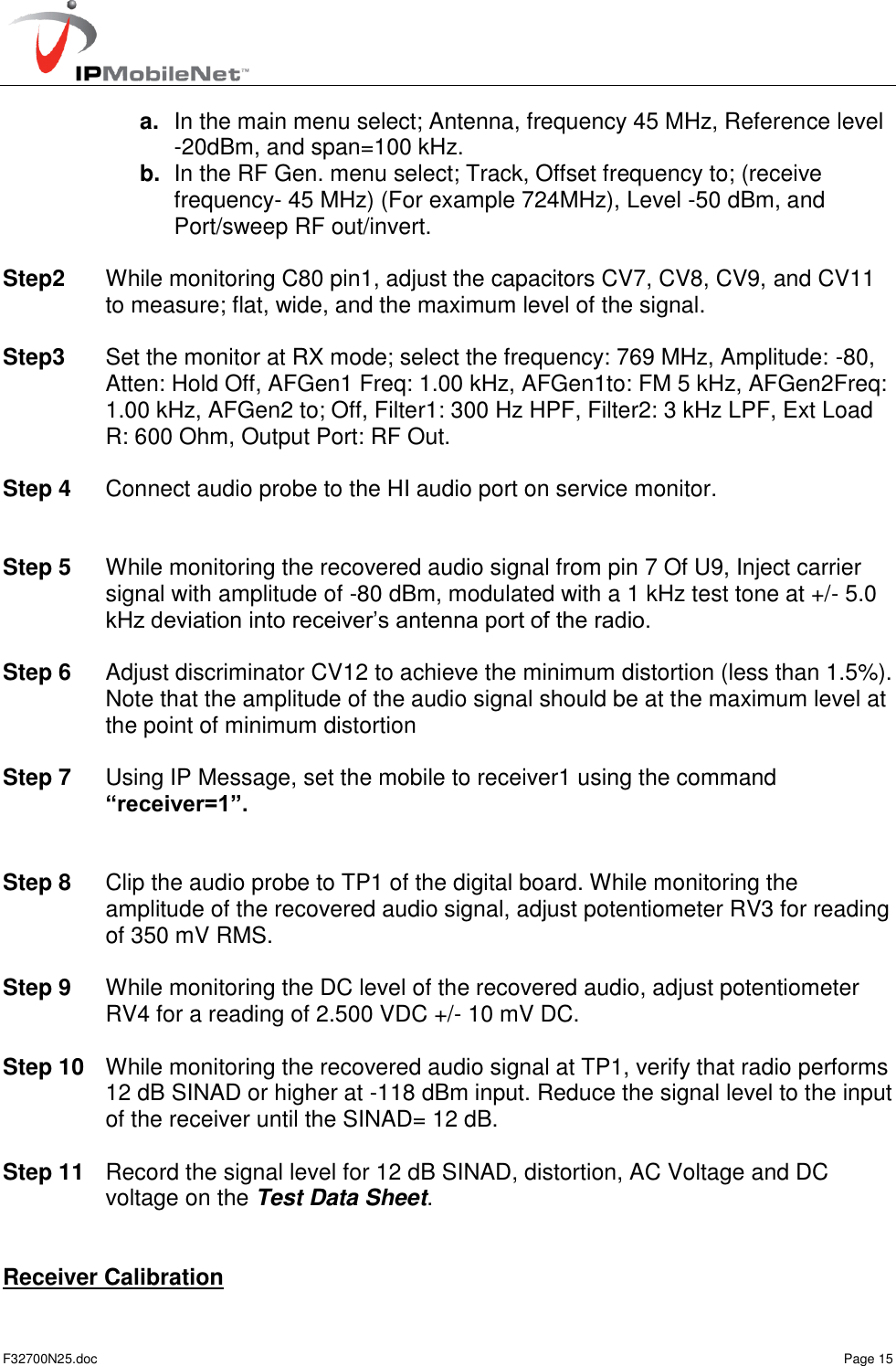
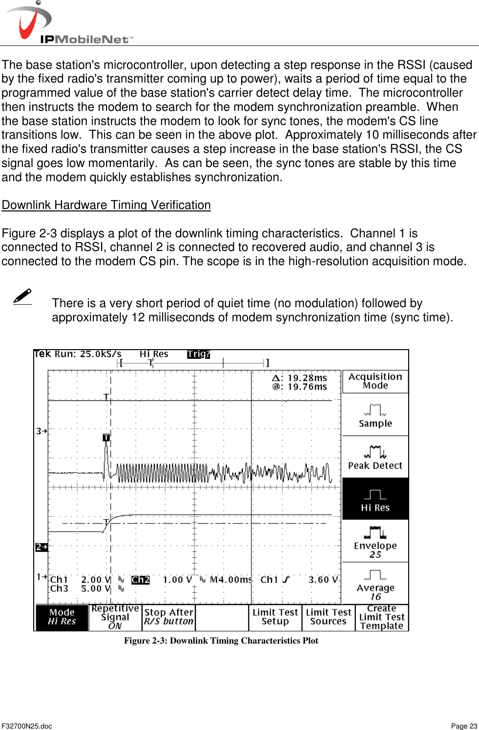
![F32700N25.doc Page 12 1 Ceramic tuning tool IPMN p/n: 44010006 1 ea #0, #1, and #2 Phillips screwdrivers (generic) Programming and Configuring the Fixed Radio Once the appropriate equipment for performing the factory test is gathered, perform the following steps to program and configure an F32700N25 Fixed Radio: Step 1 Enter the following information on the Test Data Sheet (see Appendix B): Radio Serial number Date test being performed Tester's Name Step2 Connect the power cable with a voltage source of 13.8vDC able to deliver 5 amps continuous and apply power to the mobile radio. Step 3 Program the radio to the current Firmware revision using the AVR programming utility. Step 3 Program the radio to the current Firmware revision using the AVR programming utility. Step 4 Connect a PC to the radio and launch the IPMessage program. In the IPMessage window, and verify the IP Message connection using the “?” command. Step 5 The radio will need to be unlocked using the command “Unlock=Password” using the appropriate password and placed into testmode using the command “testmode=1” for all tests unless specified otherwise. Step 6 Type „pll type=Analog Devices”. Step 7 Enter the appropriate values for the radio's frequency band. The following values were used for the fixed radio: [From: 172.16.64.1] Host serial = 115200,N,8,1, timeout=200 [From: 172.16.64.1] Channel = 0 [From: 172.16.64.1] Channel Tx freq Rx freq Inj freq](https://usermanual.wiki/IP-Mobilenet/F32700N25/User-Guide-1443545-Page-13.png)
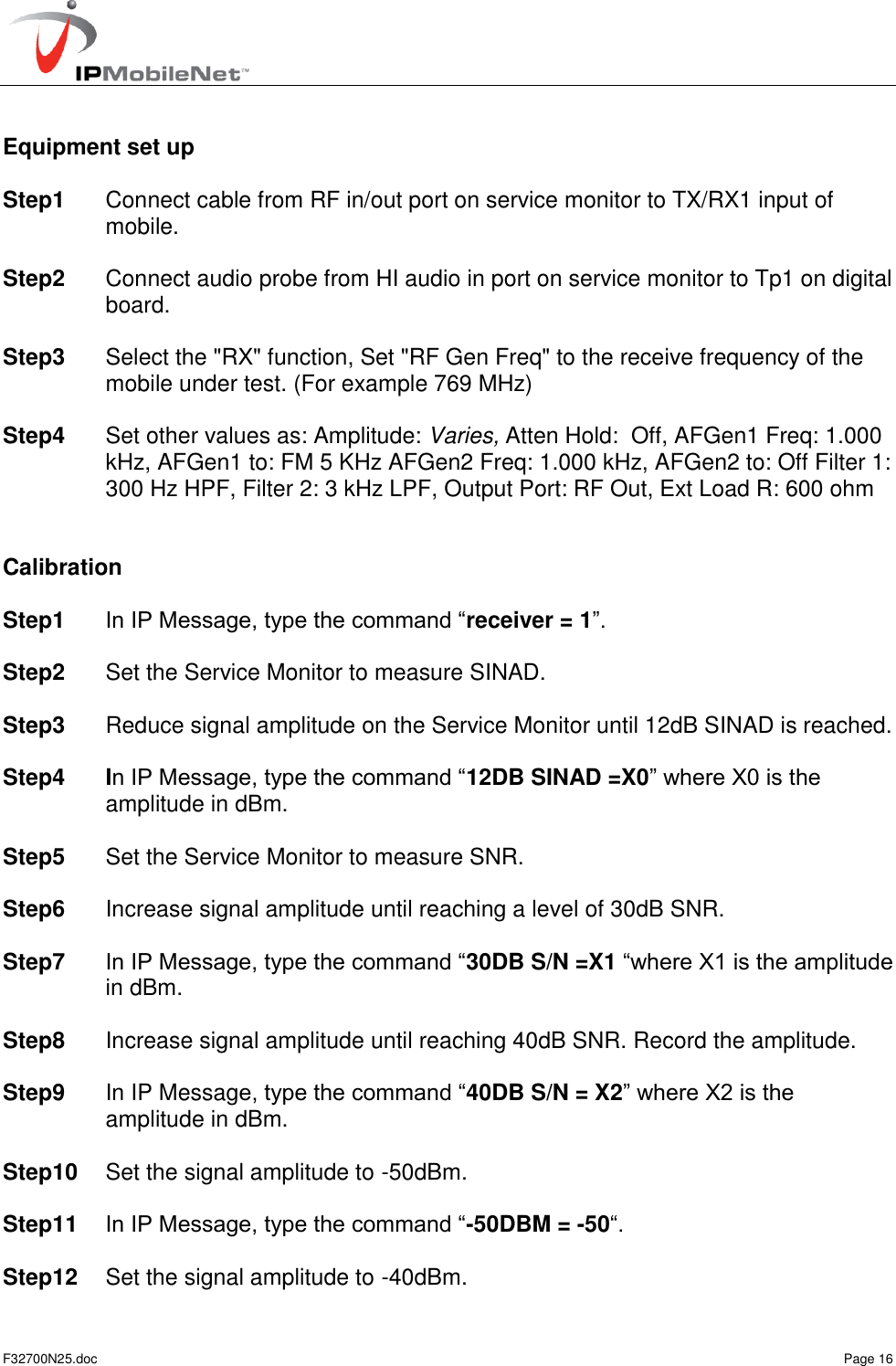
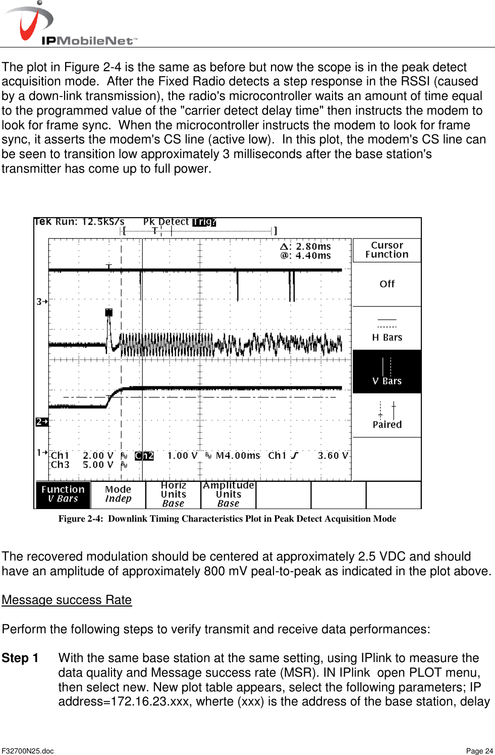
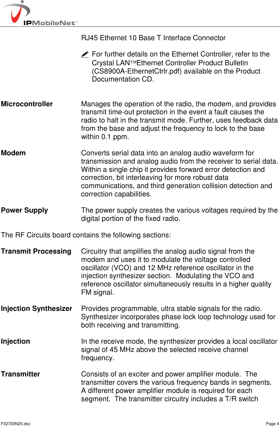
![F32700N25.doc Page 13 [From: 172.16.64.1] Frequency= 0, 799.000000 769.000000 814.000000 [From: 172.16.64.1] IP Address = 172.16.64.1 (VIU = 0.0.0.0, PC = 192.168.3.5) [From: 172.16.64.1] IPNC = 172.16.112.200 [From: 172.16.64.1] netmask = 255.255.255.0 [From: 172.16.64.1] Radio Mac Address = 00:08:ce:00:00:00 [From: 172.16.64.1] Hosting framing = SLIP no status messages [From: 172.16.64.1] channel spacing = 25000 [From: 172.16.64.1] Injection = HIGH SIDE, 45 MHz [From: 172.16.64.1] TX Power = 150 [From: 172.16.64.1] Car to car TX power = 0 [From: 172.16.64.1] serial number: undefined [From: 172.16.64.1] TX quiet time = 5 [From: 172.16.64.1] TX sync time = 2- milliseconds [From: 172.16.64.1] TX tail time = 5 [From: 172.16.64.1] TX delay = 0 slots [From: 172.16.64.1] Radio data rate = 32000 [From: 172.16.64.1] Max data tx time = 60 seconds [From: 172.16.64.1] PLL load to txkey delay = 2 milliseconds [From: 172.16.64.1] Carrier detect delay time = 6 milliseconds [From: 172.16.64.1] roam status times = 900 seconds [From: 172.16.64.1] roam lost time = 60 seconds [From: 172.16.64.1] Polarity = TX+, RX- [From: 172.16.64.1] RSSI step = 12 (=234mV) [From: 172.16.64.1] noise = -126dBm, -126dBm [From: 172.16.64.1] num timeslots = 16 [From: 172.16.64.1] timeslot period = 992ms [From: 172.16.64.1] timeslots per voice packet = 4 [From: 172.16.64.1] 06Feb2036 22:28:34 (PST), calibration=43 [From: 172.16.64.1] diversity speed = 5 [From: 172.16.64.1] receiver = AUTO [From: 172.16.64.1] Receiver Hysteresis = 2 [From: 172.16.64.1] Internal GPS Port Address = 5000 [From: 172.16.64.1] Internal GPS Input Protocol = TSIP [From: 172.16.64.1] Internal GPS Output Protocol = TSIP [From: 172.16.64.1] 12dB SINAD = -120dBm (54 on RX0) [From: 172.16.64.1] 12dB SINAD = -120dBm (54 on RX1) [From: 172.16.64.1] 30dB S/N = -106dBm (72 on RX0) [From: 172.16.64.1] 30dB S/N = -106dBm (72 on RX1) [From: 172.16.64.1] 40dB S/N = -90dBm (114 on RX0) [From: 172.16.64.1] 40dB S/N = -90dBm (114 on RX1) [From: 172.16.64.1] –40dBm = (214) on RX0) [From: 172.16.64.1] –40dBm = (214) on RX1)](https://usermanual.wiki/IP-Mobilenet/F32700N25/User-Guide-1443545-Page-14.png)
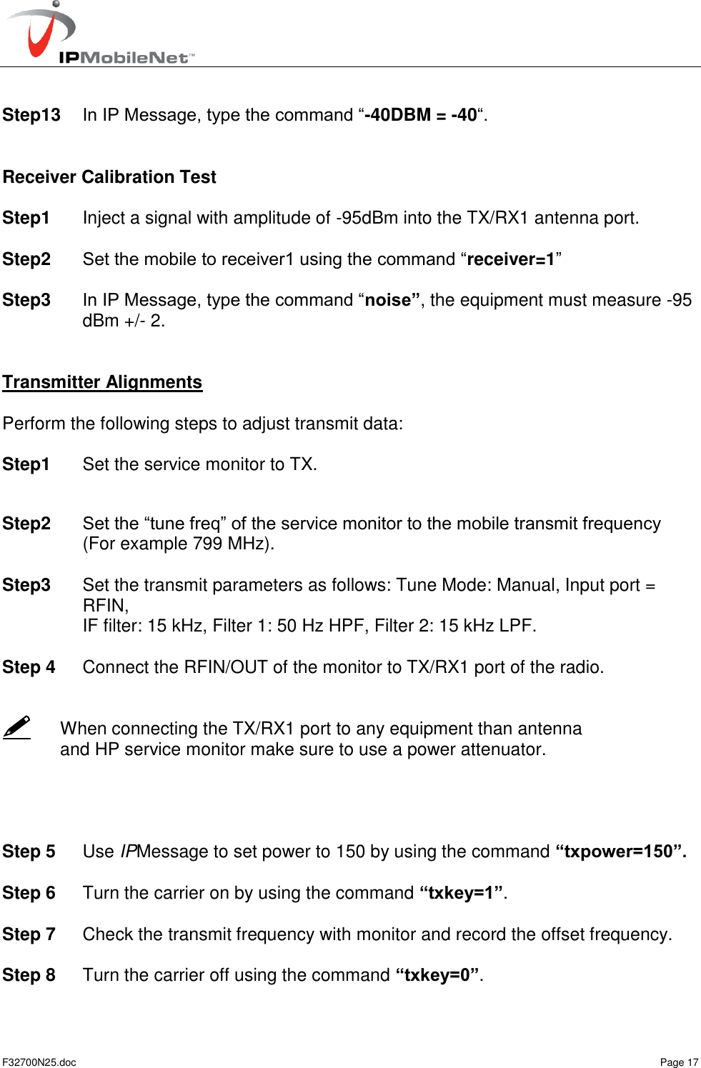
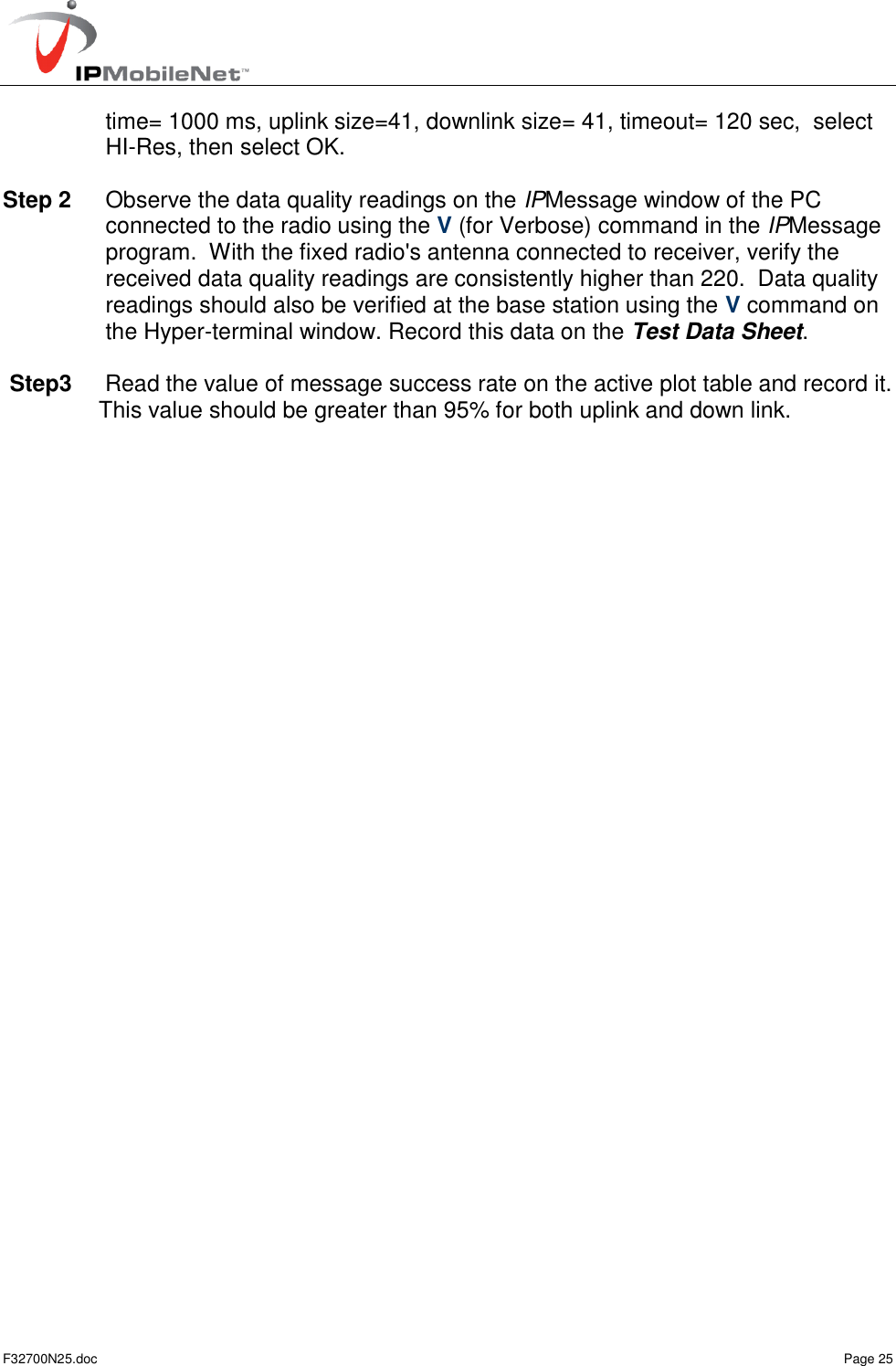
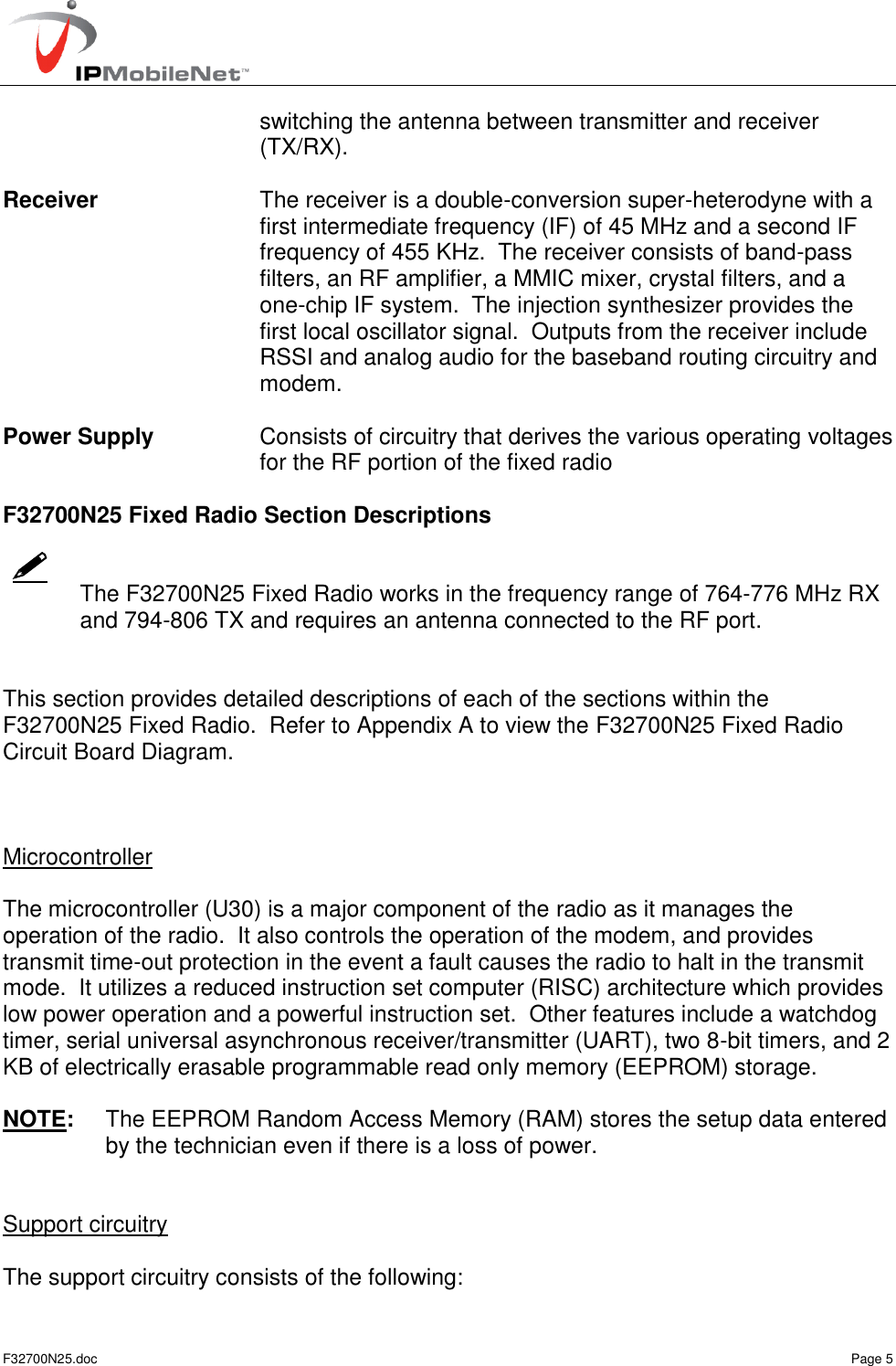
![F32700N25.doc Page 14 [From: 172.16.64.1] Suspend Tx = 0 seconds [From: 172.16.64.1] DHCP Client disabled [From: 172.16.64.1] DHCP Server disabled [From: 172.16.64.1] diag message level = 0 [From: 172.16.64.1] TFTP options = 512 (block size), 0 (interval) [From: 172.16.64.1] Internal GPS not found [From: 172.16.64.1] Modem FEC = on Adjustment / Alignment Procedures Receiver Injection Perform the following steps to adjust the receiver injection frequency: Step 1 Connect the RF output/input of HP8920 to the TX/RX antenna port of the radio and HP RF probe to the antenna port of the service monitor. Step 2 Enter the test frequency using the command ( For example “frequency=0,799,769”). Set the reference calibration using the command “reference calibration=128”. Measure the refmod voltage input to the tcxo (at JMP1). It should be close to 1.50 volts. Step 3 Select the monitor on TX measurement mode tune the measurement frequency to the injection frequency. (for example 814 MHz) Step 4 While monitoring the receiver injection frequency at RXINJ1, Select the reference calibration number by using “reference calibration = x”. Change the value of X (between 0-255) to obtain the minimum frequency error of< +/- 50 Hz. Record this value of x and the injection frequency on the Test Data Sheet. Step 5 While monitoring the 44.545 MHz 2nd injection frequency at U13 pin 4, adjust trimmer capacitor CV10 to midway between the points where the oscillation stops, then slightly turn to get the amplitude between -3 to 0 dBm. Measure the frequency and make sure that is between 44.500 and 44.590 Record this value on the Test Data Sheet. Receiver Adjustment Perform the following steps to adjust receiver: Step1 Set the monitor in spectrum analyzer mode;](https://usermanual.wiki/IP-Mobilenet/F32700N25/User-Guide-1443545-Page-15.png)