IP Mobilenet F32700N25 700/800 MHz 32k Fixed Radio User Manual
IP Mobilenet, LLC 700/800 MHz 32k Fixed Radio Users Manual
Users Manual

IPSeries
F32700N25 Fixed Radio
Product Owner‟s Manual
Date Released: March 16, 2011
Document #: 516-80618-POM Rev B
Copyright 2011 IPMobileNet, LLC.
1221 East Dyer Road, Suite # 250 Santa Ana CA 92705
Voice: (714) 434 6019 Fax: (714) 434 6019

F32700N25.doc Page ii
The term “IC”: before the radio certification number only signifies that Industry of
Canada technical specifications were met.
Operation is subject to the following two (2) conditions: (1) this devise may not cause
interference, and (2) this device must accept any interference, including interference
that may cause undesired operation of this device.
The following U.S. Patents apply to this product:
5,640,695
6,018,647
6,243,393
Information contained in this document is subject to change without notice.
All rights reserved. Reproductions, adaptations, or translation without prior written
permission is prohibited, except as allowed under copyright laws.
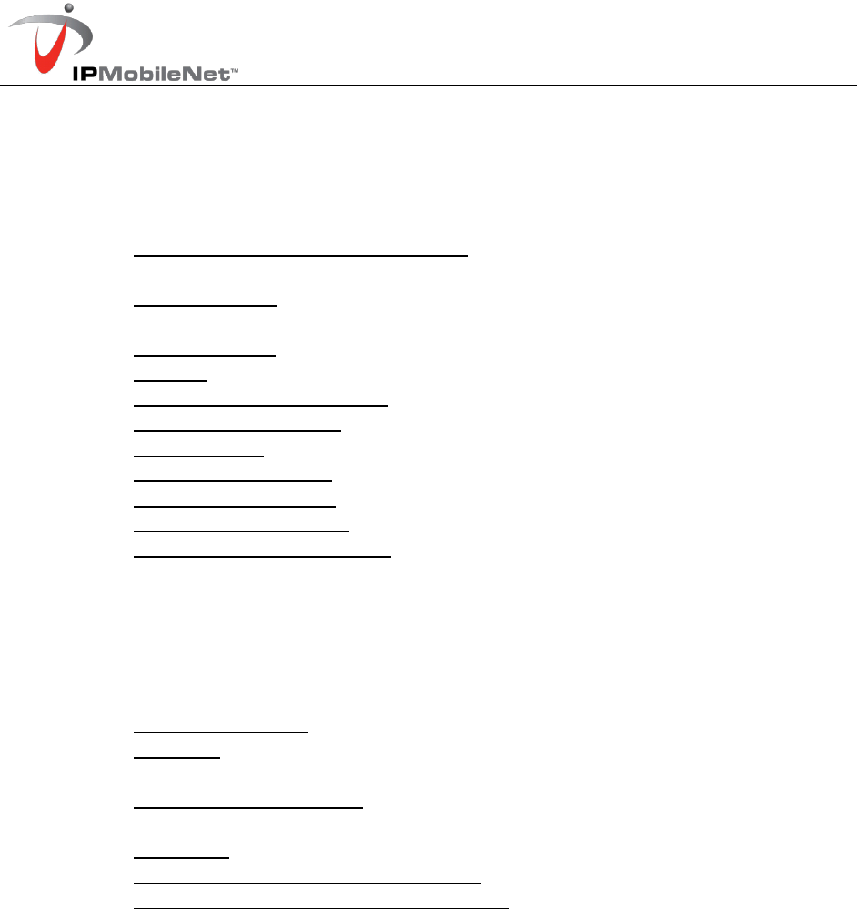
TABLE OF CONTENTS
F32700N25.doc Page 2
SECTION 1: THEORY OF OPERATION ..................................................................... 3
General Block Diagram .................................................................................... 3
General Block Diagram Definitions .......................................................... 3
F32700N25 Fixed Radio Section Descriptions ............................................... 5
Microcontroller ......................................................................................... 5
Support Circuitry .......................................................................... 5
Inputs/Outputs ......................................................................................... 5
Modem ..................................................................................................... 6
VLogic and Digital Ground ....................................................................... 6
Receiver 1 Front-End ............................................................................... 7
Receiver 1 IF ........................................................................................... 7
Transmit Modulation ................................................................................ 7
Injection Synthesizer ................................................................................ 8
Transmitter/TR Switch ............................................................................. 8
Power and Analog Ground ....................................................................... 8
SECTION 2: FACTORY TEST PROCEDURE ............................................................. 9
Equipment List .................................................................................................. 9
Programming and Configuring Fixed Radio ................................................ 10
Adjustment / Alignment Procedures ............................................................. 11
Receiver Injection .................................................................................. 11
Receiver ................................................................................................. 11
Transmit Data ........................................................................................ 12
Transmit Power Control ......................................................................... 12
Receive Data ......................................................................................... 13
Final Test ............................................................................................... 13
Uplink Hardware Timing Verification ...................................................... 15
Downlink Hardware Timing Verification ................................................. 17
SECTION 3: FCC LABEL .......................................................................................... 19
F32700N25 Data Transceiver FCC Label Placement ................................... 19
F32700N25 Data Transceiver FCC Label ...................................................... 19
APPENDIX A: F32700N25 CIRCUIT BOARD DIAGRAMS ...................................... 20
APPENDIX B: F32700N25 TEST DATA SHEET ...................................................... 21
F32700N25.doc Page 3
Section 1: Theory of Operation
Digital Board
Inputs/
outputs Micro-
controller Injection
synthesizer Receiver
Transmit
modulation Transmitter
Modem
Antenna
TR
Switch
RF Board
Transmit
Processing
Figure 1: Block Diagram
Block Diagram Definitions
For increased data security, the modem supports the Federal Government
developed Digital Encryption Standard (DES) data encryption and decryption
protocols. This capability requires installation of third party, Internet Protocol
(IP) compliant DES encryption and decryption software on the system.
The F32700N25 Fixed Radio is comprised of two (2) circuit boards, the digital board
and the RF board.
The digital circuit board contains the following sections:
Input/Output Circuitry associated with the radio’s DB9 data connector
providing all the RS232 data and handshake functions,
including the necessary level changes.

F32700N25.doc Page 4
RJ45 Ethernet 10 Base T Interface Connector
For further details on the Ethernet Controller, refer to the
Crystal LAN Ethernet Controller Product Bulletin
(CS8900A-EthernetCtrlr.pdf) available on the Product
Documentation CD.
Microcontroller Manages the operation of the radio, the modem, and provides
transmit time-out protection in the event a fault causes the
radio to halt in the transmit mode. Further, uses feedback data
from the base and adjust the frequency to lock to the base
within 0.1 ppm.
Modem Converts serial data into an analog audio waveform for
transmission and analog audio from the receiver to serial data.
Within a single chip it provides forward error detection and
correction, bit interleaving for more robust data
communications, and third generation collision detection and
correction capabilities.
Power Supply The power supply creates the various voltages required by the
digital portion of the fixed radio.
The RF Circuits board contains the following sections:
Transmit Processing Circuitry that amplifies the analog audio signal from the
modem and uses it to modulate the voltage controlled
oscillator (VCO) and 12 MHz reference oscillator in the
injection synthesizer section. Modulating the VCO and
reference oscillator simultaneously results in a higher quality
FM signal.
Injection Synthesizer Provides programmable, ultra stable signals for the radio.
Synthesizer incorporates phase lock loop technology used for
both receiving and transmitting.
Injection In the receive mode, the synthesizer provides a local oscillator
signal of 45 MHz above the selected receive channel
frequency.
Transmitter Consists of an exciter and power amplifier module. The
transmitter covers the various frequency bands in segments.
A different power amplifier module is required for each
segment. The transmitter circuitry includes a T/R switch

F32700N25.doc Page 5
switching the antenna between transmitter and receiver
(TX/RX).
Receiver The receiver is a double-conversion super-heterodyne with a
first intermediate frequency (IF) of 45 MHz and a second IF
frequency of 455 KHz. The receiver consists of band-pass
filters, an RF amplifier, a MMIC mixer, crystal filters, and a
one-chip IF system. The injection synthesizer provides the
first local oscillator signal. Outputs from the receiver include
RSSI and analog audio for the baseband routing circuitry and
modem.
Power Supply Consists of circuitry that derives the various operating voltages
for the RF portion of the fixed radio
F32700N25 Fixed Radio Section Descriptions
The F32700N25 Fixed Radio works in the frequency range of 764-776 MHz RX
and 794-806 TX and requires an antenna connected to the RF port.
This section provides detailed descriptions of each of the sections within the
F32700N25 Fixed Radio. Refer to Appendix A to view the F32700N25 Fixed Radio
Circuit Board Diagram.
Microcontroller
The microcontroller (U30) is a major component of the radio as it manages the
operation of the radio. It also controls the operation of the modem, and provides
transmit time-out protection in the event a fault causes the radio to halt in the transmit
mode. It utilizes a reduced instruction set computer (RISC) architecture which provides
low power operation and a powerful instruction set. Other features include a watchdog
timer, serial universal asynchronous receiver/transmitter (UART), two 8-bit timers, and 2
KB of electrically erasable programmable read only memory (EEPROM) storage.
NOTE: The EEPROM Random Access Memory (RAM) stores the setup data entered
by the technician even if there is a loss of power.
Support circuitry
The support circuitry consists of the following:

F32700N25.doc Page 6
A Supervisor Control Chip (U25) provides power-on reset.
The clock controls microcontroller operation and is generated by crystal Y3 and a
Pierce oscillator circuit (inside the U30-microcontroller).
The latch (U28) decodes low order address bits (A0-A7) from the address/data bits
(AD0-AD7). It is controlled by Address Latch Enable (ALE) output of U30 and the
bits are used by the modem.
A 512Kx8 Static RAM Chip (U31) provides temporary storage of the radio’s
configuration data facilitating the technician with access to make changes.
Control logic is also an important part in the microcontroller section. The RAM chip
select (RAMCS*) and modemchip select (MODEMCS*) command lines are created
by U26A, U27BCD, and U44ABC. These gates decode four (4) high order address
bits (A11-A15). The RAM is addressed by five (5) memory addresses (MA14-MA18)
bits decoded by U26D, U27A, and U24. This logic decodes port address bits (PA14-
PA18) to produce memory address bits (MA14-MA18) for the RAM chip.
Input/Output
Input/output components convert serial and handshake data from the modem section to
RS232 levels, and vice-versa. Chip U22 is an RS232 transmitter and receiver. It
converts data in 5-volt logic form to data in +/-12-volt form, as required by the RS232
standard. A charge pump power supply on the chip converts the +5-volt DC logic power
on pin 26 to the +12-volt and –12-volt levels required. Capacitors C106-C109 generate
these voltages by a charge pump. These values determine the operating voltages.
U42 is a full duplex 10base-T Ethernet controller which includes physical and MAC layer
of the protocol. Transformer T1 is the interface between analog 10 base-T signal from
the RJ45 connector and the Ethernet controller, this analog signal is then converted to
parallel data for driving the FSK modem.
Modem
The single-chip modem circuit converts parallel data to an analog audio waveform for
transmission and analog audio from a receiver to parallel data. In addition to the
modem functions, the chip provides forward error detection and correction (FEC), bit
interleaving and Viterbi Soft Decision Algorithms for more robust data communications.

F32700N25.doc Page 7
The microcontroller section controls the modem operation. Address bus, address/data
bus, and control lines operate the modem chip. The modem circuitry is also run by a
crystal-controlled clock, which consists of crystal Y1 and an internal Pierce oscillator.
The received audio signal is demodulated into digital data appearing on the AD0-AD07
lines when the MODEMCS* and RD* lines are low. The data goes to the
microcontroller section for futher processing, and then to the input/output section for
conversion to RS232 or Ethernet signal levels.
During a transmission, outgoing data appearing on the AD0-AD07 lines is converted
into a 4-level FSK analog signal by the modem chip. This operation takes place when
the MODEMCS* and WR* lines are low. Data from the user’s DTE passes through the
input/output section and microcontroller section to the AD0-AD07 bus. After processing,
data passes through a root raised cosine filter and is output to TXMOD.
This modem supports 115.2 KBPS (serial port) and 32 KBPS (over-the-air) data
transmission rates.
VLogic and Digital Ground
The VLogic and Digital Ground section consists of a pulse-width modulation (PWM)
step-down DC-DC converter (U20) that provides an adjustable output. It also reduces
noise in sensitive communications applications and minimizes drop out voltage.
An external Schottky diode (D2) is required as an output rectifier to pass inductor
current during the second half of each cycle to prevent the slow internal diode of the N-
channel MOSFET from turning on. This diode operates in pulse-frequency modulation
(PFM) mode and during transition periods while the synchronous rectifier is off.
Receiver Front-End
This section contains components that include several RF Band-pass filters, a low-noise
amplifier, and a MMIC mixer.
Incoming signals pass through one (1) pre-selector filter (FLT3) that selectively provides
a high degree of out-of-band signal rejection. A low MMIC amplifier (U4) amplifies the
selected signals and is followed by an image and noise reject filter (FLT6). The output
from FLT6 passes through a gain stage amplifier (U7) then passes through a mixer
(U8). U8 is a MMIC mixer which mixes the receive injection (RXINJ1) signal from the
synthesizer and the RF signal from the antenna to produce a 45 MHz IF signal. This 45
MHz signal passes through crystal filters (FLT3 and FLT4) to the Receiver IF section to
provide the bulk of the Receiver’s selectivity.

F32700N25.doc Page 8
Receiver IF
The major contributor of the IF subsystem (U13) a complete 45 MHz super-heterodyne
receiver chip incorporating a mixer/oscillator, two limiting intermediate frequency
amplifiers, quadrature detector, logarithmic received signal strength indicator (RSSI),
voltage regulator and audio and RSSI op amps.
Incoming 45 MHz signals appearing at RX1_45MHz pass through the low-voltage high
performance monolithic FM IF system. Within U13, the signals pass through a simple
LC filter and are boosted by the RF amplifier. The output of the RF amplifier drives a
mixer. A crystal oscillator is controlled by crystal Y2 and provides the injection
frequency for the mixer. The mixer output passes through a 455 KHz ceramic filter
(FL8). It is then amplified and passed through another ceramic filter (FL7) to a second
gain stage. One of the outputs of U13 is BRSSI1 that is the measure of receive signal
strength.
The audio is amplified by two (2) op amps (U9C and U9B) and delivered to the power
and analog ground circuitry via the RXMOD1 output. High frequency de-emphasis is
provided by a filter consisting of a resistor and a capacitor. In order to match the audio
signal levels with the other circuitry, a gain control is included. A (RV3) is necessary to
adjust gain and pot (RV4) is used to adjust the level.
Transmit Processing
The audio DC level is adjusted through OPAMP (U19), then the signal is delivered to
the transmit modulator. The reference frequency correction data is applied to DAC
(U21). The output B of the DAC then scaled down to fine tune the frequency adjustment
to about 10 ppm over the entire range of the DAC. This DC signal is applied to the OP
amps as a reference voltage.
Transmit Modulation
The analog circuitry in this section modulates the Transmitter. The data-bearing audio
signal from the modem appears at TXMOD. The audio is amplified by op amp (U23D).
The output of U23D drives two (2) amplifiers (U23B and U23C).
The transmitter uses dual-point modulation meaning the modulation is applied both to
the VCO as well as the reference oscillator (VCTXO).
The upper amplifier (U23B) has adjustable gain. The output drives op amp (U23A),
which inverts the phase of the signal. Upon the start of a transmission, the modulating
signal passes through to the VCTXO reference oscillator in the synthesizer. Some
makes of VCTXO oscillators do not require the modulation signal to be inverted and a
jumper block (JMP1) is provided to accommodate the oscillators.

F32700N25.doc Page 9
The lower op amp (U23C) amplifies the signal from the low pass filter and applies it to
the VCO via the VCOMOD output. Pots RV5 and RV5 are used to adjust maximum
deviation.
Injection Synthesizer
The fractional synthesizer chip (U17) is the major contributor of the receiver and
transmitter injection oscillator. This device contains the key components of a phase
locked loop (PLL), including a prescaler, programmable divider, and phase detector.
The selected frequencies are loaded into U17 as a clocked serial bit stream via the
PLL_DATA, PLL_CLOCK, and PLL_ENABLE signals.
Frequency stability is determined by a temperature-compensated crystal oscillator
module (VCTCXO) (TCXO1) at a frequency stability of 1 PPM from –30C to +60C.This
device has an input (REFMOD) that accepts transmit modulation and voltage from the
scaled down output of the DAC (U21). At the factory the frequency adjusted to the
nearest frequency of than 0.05 ppm accuracy and maintains the accuracy when is
locked to the base station through the correction values determined by the base station.
a voltage control oscillator (VCO1) is formed by integrated low-noise oscillators The
VCO’s generate receiver and transmit injection signals. The output of VCO1 is split by
two two-way power dividers (U16, U18) leading to outputs RXINJ1 and RXINJ2. One of
the outputs of a third two-way divider (U18) is returned to the synthesizer RFIN input.
This completes the loop signal path. The other one is the input to the driver amp of the
transmitter.
Transmitter/TR Switch
The transmitter section consists of an amplifier (U10). The output of the driver is applied
to the power amplifier (U11) to boost the power to 5 watts Max. Output A of DAC (U21)
through an Op amp. (U22A) is applied to the gain control of U11 to adjust the output
power. VBATT is applied to the Drain of U11. Harmonic suppression is provided by
C11, L10, C14, C12 and C15. Control signal TRSW is applied to pin diodes CR1, CR2
and CR3 and associated circuits to switch radio between receive and transmit mode.
Power and Analog Ground
These sections consist of the power supplies and transmit control circuitry. Power from
the vehicle’s battery appears at VBATT. Diode D1 protects the voltage regulators by
clamping any transient spikes on the supply line. Such spikes typically occur while the
engine is started. The supply line powers a series of voltage regulators and the
transmitter control circuitry, as follows:
Voltage regulator VR3 provides 8-volt power for most other sections in the radio.

F32700N25.doc Page 10
Voltage regulator U6 powers the transmit driver and T/R switch diodes as
controlled by the microcontroller.
Voltage regulator VR4 provides a low noise 3.3-volt source for the radio
electronics.
Voltage regulator VR3 provides a low noise 5-volt source for the front end
amplifiers (U4 and U7) , mixer (U8) and Receive audio OP amp (U9).

F32700N25.doc Page 11
Section 2: Test Procedure
Equipment List
The following table lists the equipment required to perform the F32700N25Fixed Radio
Factory Test Procedure:
QTY
DESCRIPTION
MANUFACTURER
MODEL
2
PC’s
One for Fixed
One for Base
Windows 9X w/
IPMessage
AVR
1
Service Monitor –
Communication Test Set
HP
HP8920B
or
equivalent
1
Digital multi-meter
Tektronix
Fluke
77 or
equivalent
1
DC power supply w/
ammeter, 13.8V, 23 Amps or
more
Astron
RM35A
1
4-Channel Scope
Tektronix
TDS 460A
1
F32700N25 Fixed Radio
1
B64700G-25 Calibrated
Base Station
1
Internet Protocol Network
Controller (IPNC)
1
25 watt dummy
load/attenuator
Bird Electronic
25-A-MFN-
20 or
equivalent
2
700 MHz Antennas (generic
mag mount)
1
Serial cable DB9M-DB9F
connectors
IPMN p/n:
156-0245-
020
1
IP power cable
IPMN p/n:
502-
82017-52
1
3-foot RF jumper cable with
type N connectors (generic)
1
Scope test probe (generic,
X1 attenuation)

F32700N25.doc Page 12
1
Ceramic tuning tool
IPMN p/n:
44010006
1 ea
#0, #1, and #2 Phillips
screwdrivers (generic)
Programming and Configuring the Fixed Radio
Once the appropriate equipment for performing the factory test is gathered, perform the
following steps to program and configure an F32700N25 Fixed Radio:
Step 1 Enter the following information on the Test Data Sheet (see Appendix B):
Radio Serial number
Date test being performed
Tester's Name
Step2 Connect the power cable with a voltage source of 13.8vDC able to deliver 5
amps continuous and apply power to the mobile radio.
Step 3 Program the radio to the current Firmware revision using the AVR
programming utility.
Step 3 Program the radio to the current Firmware revision using the AVR
programming utility.
Step 4 Connect a PC to the radio and launch the IPMessage program. In the
IPMessage window, and verify the IP Message connection using the “?”
command.
Step 5 The radio will need to be unlocked using the command “Unlock=Password”
using the appropriate password and placed into testmode using the command
“testmode=1” for all tests unless specified otherwise.
Step 6 Type „pll type=Analog Devices”.
Step 7 Enter the appropriate values for the radio's frequency band. The following
values were used for the fixed radio:
[From: 172.16.64.1] Host serial = 115200,N,8,1, timeout=200
[From: 172.16.64.1] Channel = 0
[From: 172.16.64.1] Channel Tx freq Rx freq
Inj freq

F32700N25.doc Page 13
[From: 172.16.64.1] Frequency= 0, 799.000000 769.000000
814.000000
[From: 172.16.64.1] IP Address = 172.16.64.1 (VIU = 0.0.0.0,
PC = 192.168.3.5)
[From: 172.16.64.1] IPNC = 172.16.112.200
[From: 172.16.64.1] netmask = 255.255.255.0
[From: 172.16.64.1] Radio Mac Address = 00:08:ce:00:00:00
[From: 172.16.64.1] Hosting framing = SLIP no status
messages
[From: 172.16.64.1] channel spacing = 25000
[From: 172.16.64.1] Injection = HIGH SIDE, 45 MHz
[From: 172.16.64.1] TX Power = 150
[From: 172.16.64.1] Car to car TX power = 0
[From: 172.16.64.1] serial number: undefined
[From: 172.16.64.1] TX quiet time = 5
[From: 172.16.64.1] TX sync time = 2- milliseconds
[From: 172.16.64.1] TX tail time = 5
[From: 172.16.64.1] TX delay = 0 slots
[From: 172.16.64.1] Radio data rate = 32000
[From: 172.16.64.1] Max data tx time = 60 seconds
[From: 172.16.64.1] PLL load to txkey delay = 2 milliseconds
[From: 172.16.64.1] Carrier detect delay time = 6 milliseconds
[From: 172.16.64.1] roam status times = 900 seconds
[From: 172.16.64.1] roam lost time = 60 seconds
[From: 172.16.64.1] Polarity = TX+, RX-
[From: 172.16.64.1] RSSI step = 12 (=234mV)
[From: 172.16.64.1] noise = -126dBm, -126dBm
[From: 172.16.64.1] num timeslots = 16
[From: 172.16.64.1] timeslot period = 992ms
[From: 172.16.64.1] timeslots per voice packet = 4
[From: 172.16.64.1] 06Feb2036 22:28:34 (PST), calibration=43
[From: 172.16.64.1] diversity speed = 5
[From: 172.16.64.1] receiver = AUTO
[From: 172.16.64.1] Receiver Hysteresis = 2
[From: 172.16.64.1] Internal GPS Port Address = 5000
[From: 172.16.64.1] Internal GPS Input Protocol = TSIP
[From: 172.16.64.1] Internal GPS Output Protocol = TSIP
[From: 172.16.64.1] 12dB SINAD = -120dBm (54 on RX0)
[From: 172.16.64.1] 12dB SINAD = -120dBm (54 on RX1)
[From: 172.16.64.1] 30dB S/N = -106dBm (72 on RX0)
[From: 172.16.64.1] 30dB S/N = -106dBm (72 on RX1)
[From: 172.16.64.1] 40dB S/N = -90dBm (114 on RX0)
[From: 172.16.64.1] 40dB S/N = -90dBm (114 on RX1)
[From: 172.16.64.1] –40dBm = (214) on RX0)
[From: 172.16.64.1] –40dBm = (214) on RX1)

F32700N25.doc Page 14
[From: 172.16.64.1] Suspend Tx = 0 seconds
[From: 172.16.64.1] DHCP Client disabled
[From: 172.16.64.1] DHCP Server disabled
[From: 172.16.64.1] diag message level = 0
[From: 172.16.64.1] TFTP options = 512 (block size), 0
(interval)
[From: 172.16.64.1] Internal GPS not found
[From: 172.16.64.1] Modem FEC = on
Adjustment / Alignment Procedures
Receiver Injection
Perform the following steps to adjust the receiver injection frequency:
Step 1 Connect the RF output/input of HP8920 to the TX/RX antenna port of the
radio and HP RF probe to the antenna port of the service monitor.
Step 2 Enter the test frequency using the command ( For example
“frequency=0,799,769”). Set the reference calibration using the command
“reference calibration=128”. Measure the refmod voltage input to the tcxo
(at JMP1). It should be close to 1.50 volts.
Step 3 Select the monitor on TX measurement mode tune the measurement
frequency to the injection frequency. (for example 814 MHz)
Step 4 While monitoring the receiver injection frequency at RXINJ1, Select the
reference calibration number by using “reference calibration = x”. Change
the value of X (between 0-255) to obtain the minimum frequency error of< +/-
50 Hz. Record this value of x and the injection frequency on the Test Data
Sheet.
Step 5 While monitoring the 44.545 MHz 2nd injection frequency at U13 pin 4, adjust
trimmer capacitor CV10 to midway between the points where the oscillation
stops, then slightly turn to get the amplitude between -3 to 0 dBm. Measure
the frequency and make sure that is between 44.500 and 44.590 Record this
value on the Test Data Sheet.
Receiver Adjustment
Perform the following steps to adjust receiver:
Step1 Set the monitor in spectrum analyzer mode;

F32700N25.doc Page 15
a. In the main menu select; Antenna, frequency 45 MHz, Reference level
-20dBm, and span=100 kHz.
b. In the RF Gen. menu select; Track, Offset frequency to; (receive
frequency- 45 MHz) (For example 724MHz), Level -50 dBm, and
Port/sweep RF out/invert.
Step2 While monitoring C80 pin1, adjust the capacitors CV7, CV8, CV9, and CV11
to measure; flat, wide, and the maximum level of the signal.
Step3 Set the monitor at RX mode; select the frequency: 769 MHz, Amplitude: -80,
Atten: Hold Off, AFGen1 Freq: 1.00 kHz, AFGen1to: FM 5 kHz, AFGen2Freq:
1.00 kHz, AFGen2 to; Off, Filter1: 300 Hz HPF, Filter2: 3 kHz LPF, Ext Load
R: 600 Ohm, Output Port: RF Out.
Step 4 Connect audio probe to the HI audio port on service monitor.
Step 5 While monitoring the recovered audio signal from pin 7 Of U9, Inject carrier
signal with amplitude of -80 dBm, modulated with a 1 kHz test tone at +/- 5.0
kHz deviation into receiver’s antenna port of the radio.
Step 6 Adjust discriminator CV12 to achieve the minimum distortion (less than 1.5%).
Note that the amplitude of the audio signal should be at the maximum level at
the point of minimum distortion
Step 7 Using IP Message, set the mobile to receiver1 using the command
“receiver=1”.
Step 8 Clip the audio probe to TP1 of the digital board. While monitoring the
amplitude of the recovered audio signal, adjust potentiometer RV3 for reading
of 350 mV RMS.
Step 9 While monitoring the DC level of the recovered audio, adjust potentiometer
RV4 for a reading of 2.500 VDC +/- 10 mV DC.
Step 10 While monitoring the recovered audio signal at TP1, verify that radio performs
12 dB SINAD or higher at -118 dBm input. Reduce the signal level to the input
of the receiver until the SINAD= 12 dB.
Step 11 Record the signal level for 12 dB SINAD, distortion, AC Voltage and DC
voltage on the Test Data Sheet.
Receiver Calibration

F32700N25.doc Page 16
Equipment set up
Step1 Connect cable from RF in/out port on service monitor to TX/RX1 input of
mobile.
Step2 Connect audio probe from HI audio in port on service monitor to Tp1 on digital
board.
Step3 Select the "RX" function, Set "RF Gen Freq" to the receive frequency of the
mobile under test. (For example 769 MHz)
Step4 Set other values as: Amplitude: Varies, Atten Hold: Off, AFGen1 Freq: 1.000
kHz, AFGen1 to: FM 5 KHz AFGen2 Freq: 1.000 kHz, AFGen2 to: Off Filter 1:
300 Hz HPF, Filter 2: 3 kHz LPF, Output Port: RF Out, Ext Load R: 600 ohm
Calibration
Step1 In IP Message, type the command “receiver = 1”.
Step2 Set the Service Monitor to measure SINAD.
Step3 Reduce signal amplitude on the Service Monitor until 12dB SINAD is reached.
Step4 In IP Message, type the command “12DB SINAD =X0” where X0 is the
amplitude in dBm.
Step5 Set the Service Monitor to measure SNR.
Step6 Increase signal amplitude until reaching a level of 30dB SNR.
Step7 In IP Message, type the command “30DB S/N =X1 “where X1 is the amplitude
in dBm.
Step8 Increase signal amplitude until reaching 40dB SNR. Record the amplitude.
Step9 In IP Message, type the command “40DB S/N = X2” where X2 is the
amplitude in dBm.
Step10 Set the signal amplitude to -50dBm.
Step11 In IP Message, type the command “-50DBM = -50“.
Step12 Set the signal amplitude to -40dBm.

F32700N25.doc Page 17
Step13 In IP Message, type the command “-40DBM = -40“.
Receiver Calibration Test
Step1 Inject a signal with amplitude of -95dBm into the TX/RX1 antenna port.
Step2 Set the mobile to receiver1 using the command “receiver=1”
Step3 In IP Message, type the command “noise”, the equipment must measure -95
dBm +/- 2.
Transmitter Alignments
Perform the following steps to adjust transmit data:
Step1 Set the service monitor to TX.
Step2 Set the “tune freq” of the service monitor to the mobile transmit frequency
(For example 799 MHz).
Step3 Set the transmit parameters as follows: Tune Mode: Manual, Input port =
RFIN,
IF filter: 15 kHz, Filter 1: 50 Hz HPF, Filter 2: 15 kHz LPF.
Step 4 Connect the RFIN/OUT of the monitor to TX/RX1 port of the radio.
When connecting the TX/RX1 port to any equipment than antenna
and HP service monitor make sure to use a power attenuator.
Step 5 Use IPMessage to set power to 150 by using the command “txpower=150”.
Step 6 Turn the carrier on by using the command “txkey=1”.
Step 7 Check the transmit frequency with monitor and record the offset frequency.
Step 8 Turn the carrier off using the command “txkey=0”.

F32700N25.doc Page 18
Step 9 Turn potentiometer RV5 fully counterclockwise.
Step 10 Turn on the modulated transmit signal using transmit command “x = 1400,
19”
Step 11 Adjust RV6 for deviation of 4.9 kHz.
Step 12 Select the right combination of polarity for transmit and receive signals TX+/-
RX+/- out of four possible choices.
Step13 Using calibrated base station at the paired frequency, and monitoring the
uplink received data quality on the base station's Hyperterminal screen. With
the correct selection in step 12 the base station will receive data and the
carrier detect (green light) turns on. Slowly turn RV5 clockwise until consistent
data quality readings of 220 - 248 are achieved using 1400 character test
messages. Data quality reading should not be less than 220 for 1400
character messages.
If unable to reach the data quality readings then ask for Technical
Support. Poor data quality readings are indicative of poor group
delay performance, or other defect.
Step 14 Verify transmit deviation, frequency error, and transmitting data messages
quality and record this data on the Test Data Sheet.
Power Setting
Perform the following steps to adjust the transmit power control:
Step 1 Using the “ txkey=1” command of IPMessage, and while monitoring the
transmit power level on the HP communications test set, send the txpower=
x command to adjust the power level settings to slightly less than 5 Watts of
output power is obtained. Record this value on the Test Data Sheet.
Step 2 Adjust “maximum txpower = x”to the value that output power does not
exceed 5.0 Watts. Record this value on the Test Data Sheet.
Do not to exceed 5 Watts of output power, as this may reduce the life of PA.

F32700N25.doc Page 19
Final Test
A final test must be performed prior to shipping the F32700N25 Fixed Radio to the
customer. This final test will verify that the timing characteristics are correct and that
both transmit and receive data quality readings are consistently high.
Perform the following steps for the final test:
Step 1 Attach the 20dB 25Watt power attenuator to the transmit port of the radio.
Step 2 Program the radio for full power operation. The tx power level setting can be
found in the radio's Test Data Sheet.
The setting must not to exceed 5 Watts.
Step 3 Attach a digital scope to the base station as described in section the next
section, Uplink Hardware Timing Verification. Using the x=1400,19
command (which will cause the radio to transmit 19, 1400 character
messages), verify the following:
Transmit frequency of radio is adjusted for minimum frequency error of <+/-
100 Hz.
The x=1400,19 command will generate different messages with differing DC
components. Each message will slightly slew the frequency off from the
center frequency). Be careful to closely monitor the variation in transmit
frequency due to these different messages and ensure that on average the
transit frequency error has been minimized to within +/-100 Hz. This indicates
that some of these test messages will be slightly high in frequency, some
messages will be slightly low in frequency, and some messages will be right
on frequency.
Step 4 Verify the transmit deviation is 4.9 kHz
Step 5 Verify the timing characteristics are identical to the plots in the next section,
Uplink Hardware Timing Verification.
Step 6 At the base station monitor PC, verify that all the data quality readings are
240 and higher.
Step 7 Move the scope probes to monitor the timing at the Fixed Radio as described
in Downlink Hardware Timing Verification. Generate test messages by
pinging the IPNC from the PC attached to the radio. The following command

F32700N25.doc Page 20
will cause 100 pings, 500 bytes in length to be transmitted from the Fixed
Radio and echoed by the IPNC through the base station:
.>;Ping 192.168.3.3 -n 100 -l 500 -w 2000
Step 8 Set CRC =1 Enable on the radio
Step 9 Verify the timing characteristics are identical to those in Downlink Hardware
Timing Verification.
Step 10 Reset CRC = 0 Disable on the radio
Step 11 In IPMessage, type the ? command to radio. Copy the radio settings and
paste them into the Test Data File.
Step 13 Perform a close visual inspection of the radio closely inspecting
manufacturing related problems (loose screws, solder particles, etc.).
F32700N25.doc Page 21
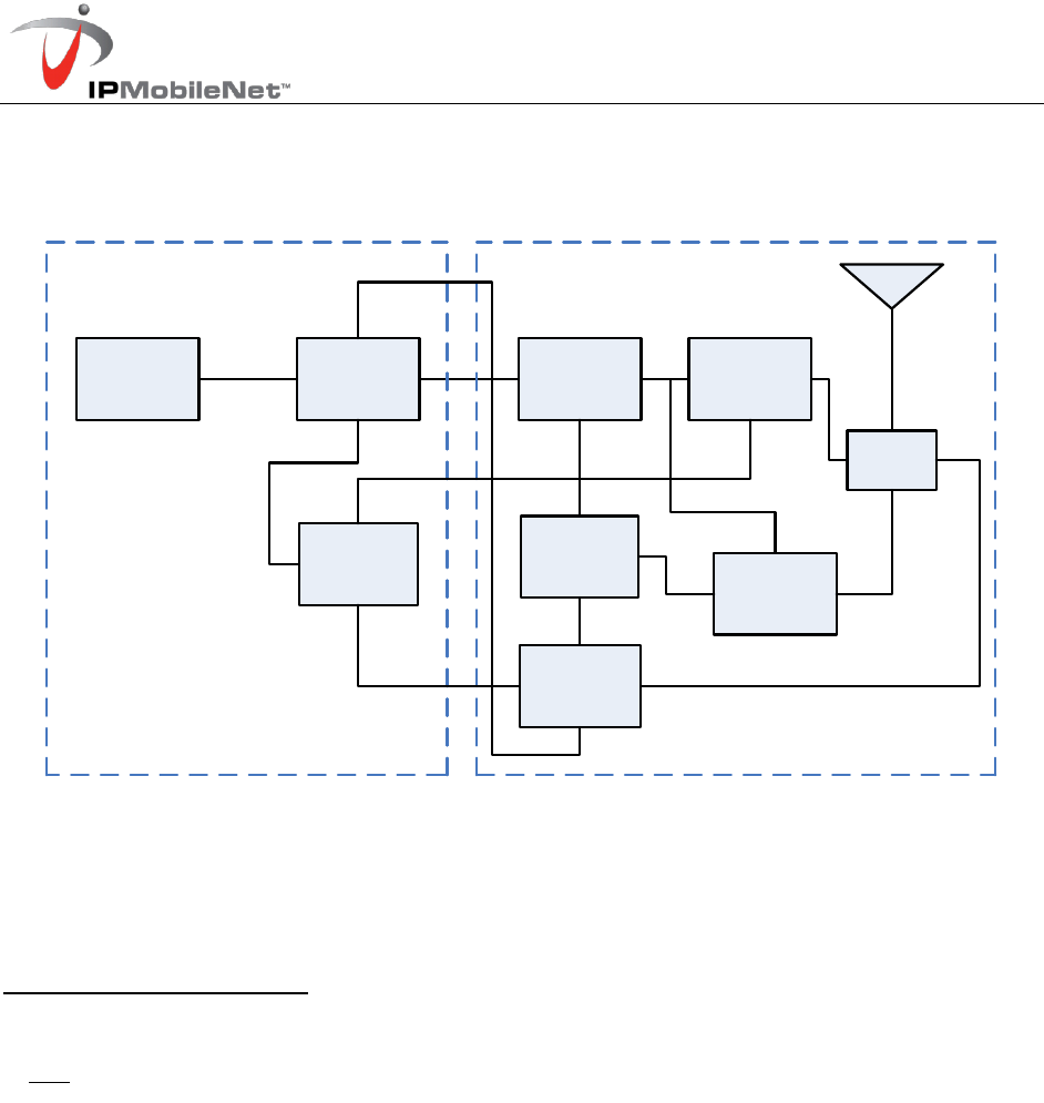
Uplink Hardware Timing Verification
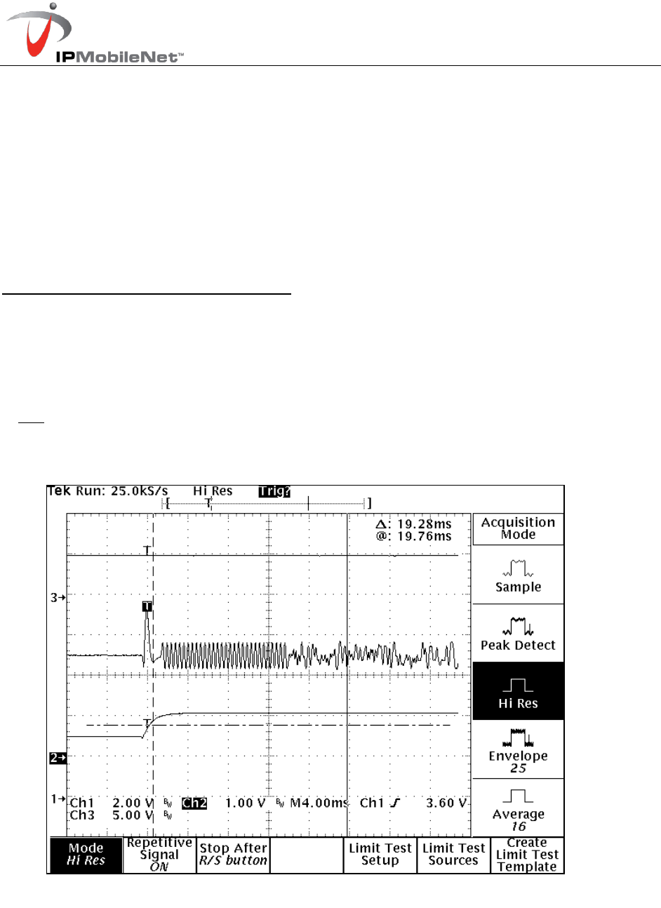
Figure 2-1 below displays an oscilloscope plot of an uplink data message from the Fixed
Radio to the base station. Channel 1 is connected to the base station's RSSI (XXX-12),
channel 2 is connected to the base station's recovered modulation, and channel 3 is
connected to the base station's modem chip select line. The scopes acquisition mode is
high-resolution.
Figure 2-1: Oscilloscope Plot of an Uplink Data Message
F32700N25.doc Page 22
As seen in the above plot, the fixed radio's transmit carrier has ramped up to full power
(channel 1) in just a few milliseconds. The recovered modulation (channel 2) is stable
by this time. There follows a few milliseconds of quiet time followed by 12 milliseconds
of symbol sync time.
The recovered modulation from a Fixed Radio should look identical to this
plot. The recovered modulation signal should be approximately 1.0 Volts
peak-to-peak and should be centered at approximately 2.5 VDC as is
indicated in the figure above.
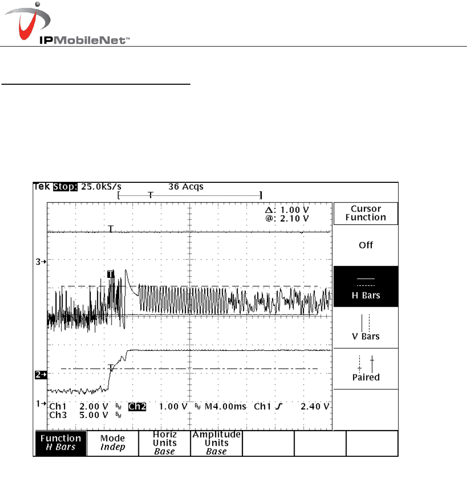
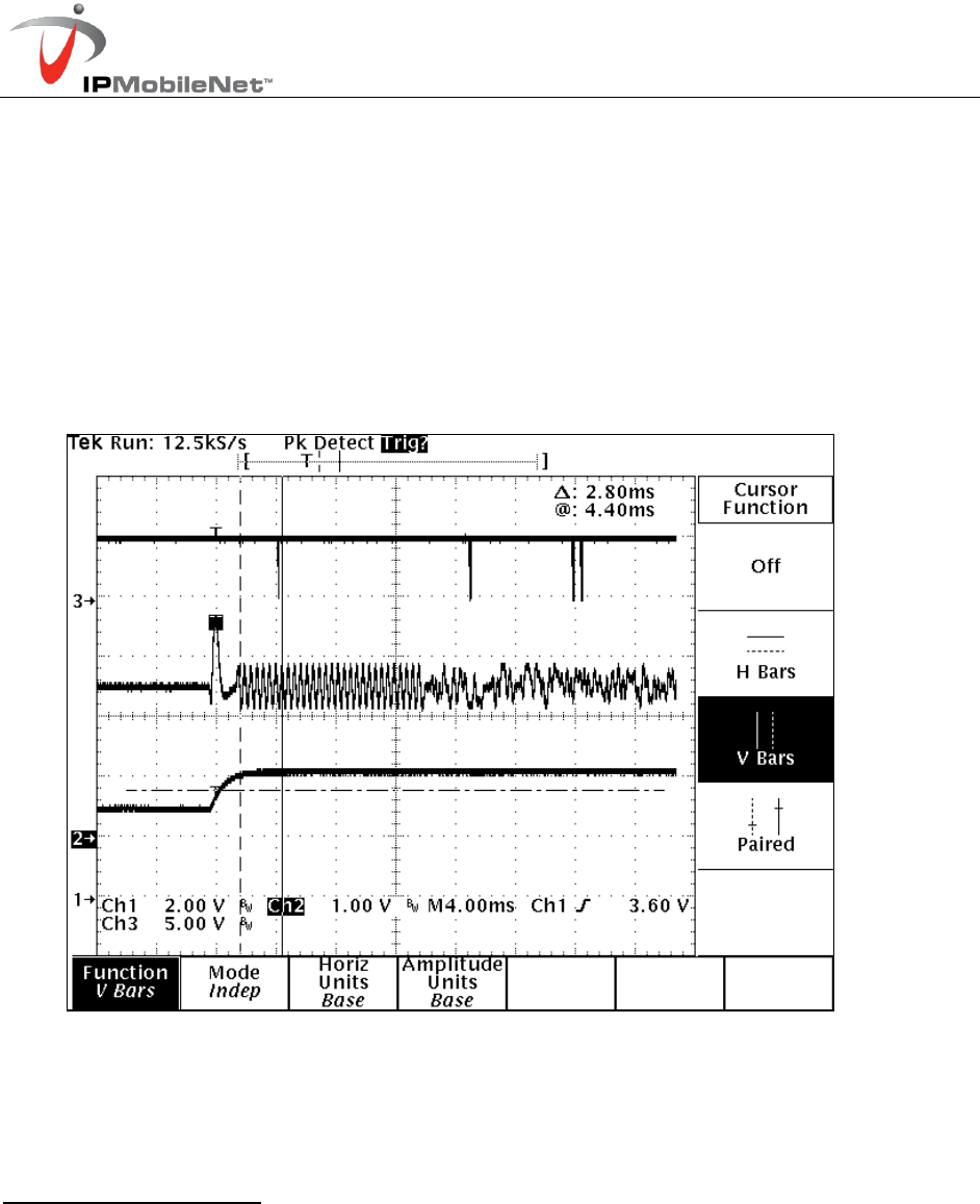
Figure 2-2 displays another oscilloscope plot of an up-link data message from the Fixed
Radio to the base station. As in the last plot, channel 1 is connected to the base
station's RSSI (J5-12), channel 2 is connected to the base station's recovered
modulation test point, and channel 3 is connected to the base station's modem chip
select line (U16-13). The scope's acquisition mode is now in the peak detect mode.
This enables the base station's modem CS (Chip Select) line to be viewed.
Figure 2-2: Another Oscilloscope Plot of an Uplink Data Message
F32700N25.doc Page 23
The base station's microcontroller, upon detecting a step response in the RSSI (caused
by the fixed radio's transmitter coming up to power), waits a period of time equal to the
programmed value of the base station's carrier detect delay time. The microcontroller
then instructs the modem to search for the modem synchronization preamble. When
the base station instructs the modem to look for sync tones, the modem's CS line
transitions low. This can be seen in the above plot. Approximately 10 milliseconds after
the fixed radio's transmitter causes a step increase in the base station's RSSI, the CS
signal goes low momentarily. As can be seen, the sync tones are stable by this time
and the modem quickly establishes synchronization.
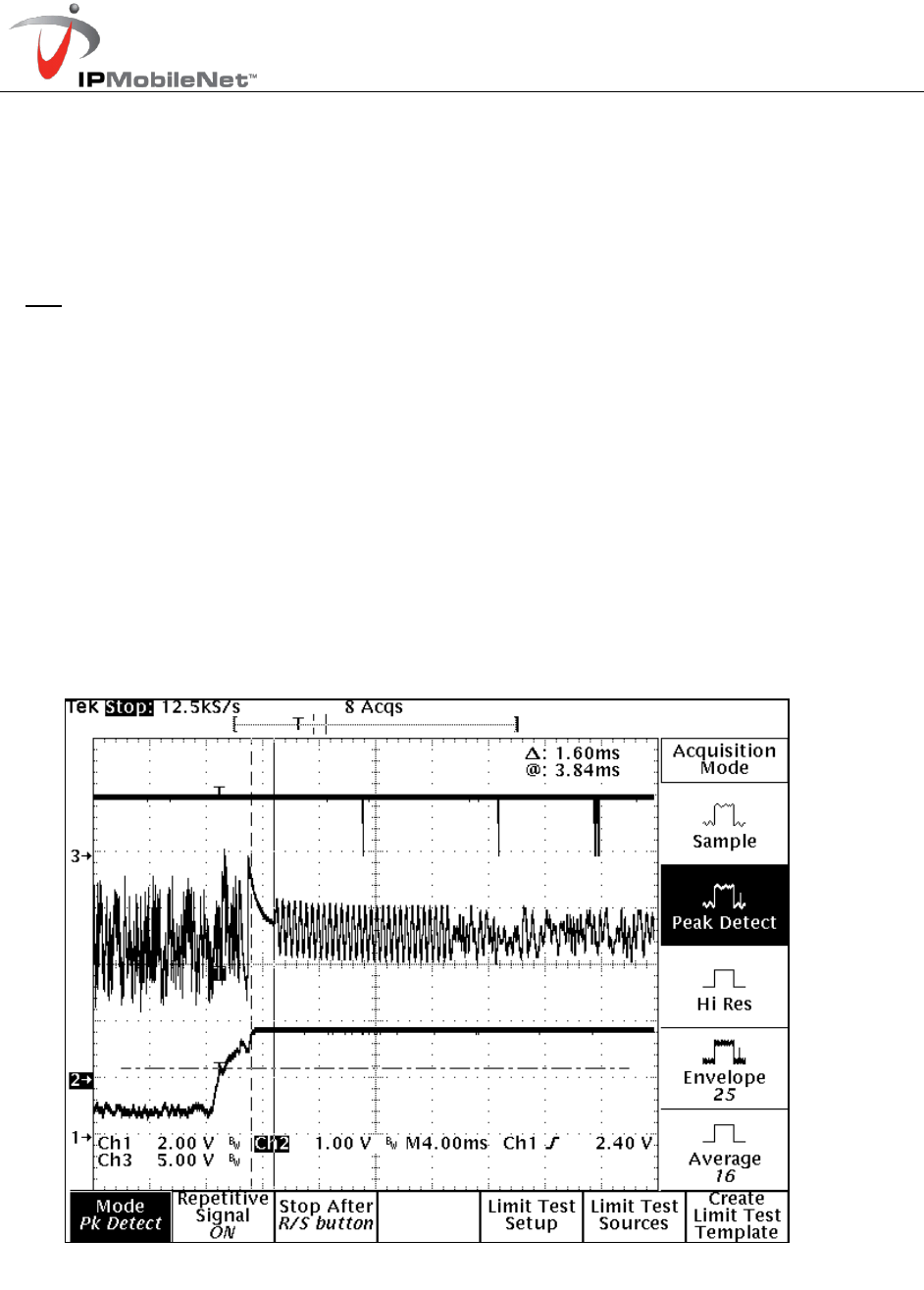
Downlink Hardware Timing Verification
Figure 2-3 displays a plot of the downlink timing characteristics. Channel 1 is
connected to RSSI, channel 2 is connected to recovered audio, and channel 3 is
connected to the modem CS pin. The scope is in the high-resolution acquisition mode.
There is a very short period of quiet time (no modulation) followed by
approximately 12 milliseconds of modem synchronization time (sync time).
Figure 2-3: Downlink Timing Characteristics Plot
F32700N25.doc Page 24
The plot in Figure 2-4 is the same as before but now the scope is in the peak detect
acquisition mode. After the Fixed Radio detects a step response in the RSSI (caused
by a down-link transmission), the radio's microcontroller waits an amount of time equal
to the programmed value of the "carrier detect delay time" then instructs the modem to
look for frame sync. When the microcontroller instructs the modem to look for frame
sync, it asserts the modem's CS line (active low). In this plot, the modem's CS line can
be seen to transition low approximately 3 milliseconds after the base station's
transmitter has come up to full power.
The recovered modulation should be centered at approximately 2.5 VDC and should
have an amplitude of approximately 800 mV peal-to-peak as indicated in the plot above.
Message success Rate
Perform the following steps to verify transmit and receive data performances:
Step 1 With the same base station at the same setting, using IPlink to measure the
data quality and Message success rate (MSR). IN IPlink open PLOT menu,
then select new. New plot table appears, select the following parameters; IP
address=172.16.23.xxx, wherte (xxx) is the address of the base station, delay
Figure 2-4: Downlink Timing Characteristics Plot in Peak Detect Acquisition Mode

F32700N25.doc Page 25
time= 1000 ms, uplink size=41, downlink size= 41, timeout= 120 sec, select
HI-Res, then select OK.
Step 2 Observe the data quality readings on the IPMessage window of the PC
connected to the radio using the V (for Verbose) command in the IPMessage
program. With the fixed radio's antenna connected to receiver, verify the
received data quality readings are consistently higher than 220. Data quality
readings should also be verified at the base station using the V command on
the Hyper-terminal window. Record this data on the Test Data Sheet.
Step3 Read the value of message success rate on the active plot table and record it.
This value should be greater than 95% for both uplink and down link.
SECTION 3: FCC LABEL
F32700N25.doc Page 26
Section 3: FCC / IC Label
F32700N25 Data Transceiver FCC / IC Label Placement
F32700N25 Data Transceiver FCC Label
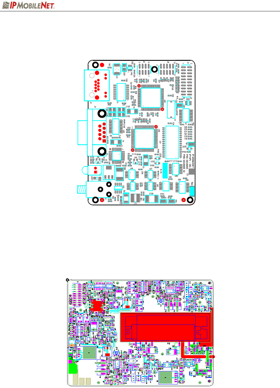
APPENDIX A: CIRCUIT BOARD LAYOUTS
F32700N25-FCCRpt.doc Page 27
F32700N25Fixed Radio Digital Circuit Board
F32700N25Fixed Radio RF Circuit Board
+
+
++
+
+
+

APPENDIX B: F32700N25 TEST DATA SHEET
F32700N25-FCCRpt.doc Page 28
Program and Configure Radio
Date
Serial Number
Firmware Revision
Tester
Adjustment / Alignment Procedures
Receiver Injection
Parameter
Spec
Measured
Injection Frequency Error at
RXINJ1(within +/- 100 Hz of exact
injection frequency)
+/- 100 Hz
U13 pin 4 power level
-3 to -5 dBm
Receiver
Parameter
Spec
Receiver
Measured
Audio DC Amplitude
(1 kHz Test tone @ 5.0 kHz
Deviation)
2.5 VDC
+/- 1mV
Audio AC Amplitude
(1 kHz Test tone @ 5.0 kHz
Deviation)
350 mVRMS
+/- 10mV
Distortion
(1 kHz Test tone @ 5.0 kHz
Deviation)
2%<
SINAD 12 dB
(1 kHz Test tone @ 5.0 kHz
Deviation)
-118dBm >

APPENDIX B: F32700N25 TEST DATA SHEET
F32700N25-FCCRpt.doc Page 29
Transmit Section
Parameter
Spec
Measured
Transmit Modulation Deviation
(4.9 kHz while transmitting 1400 character test
message)
4.9 kHz
Transmit Data Quality
(While transmitting 1400 character test
messages to the base station)
220 >
Transmit Power Control
Caution: Donot to exceed 5-Watts RF output power during this test.
Transmit Power
Setting
Expected RF Out
RF Out Watts
0
25
50
75
100
125
150
175
200
225
250
Do not to exceed 5 Watts of output power.
Parameter
Digital Code
Measure
Maximum power output setting without
exceeding 5.0Watts

APPENDIX B: F32700N25 TEST DATA SHEET
F32700N25-FCCRpt.doc Page 30
Data Quality
Parameter
Spec
Measured
Receiver Data Quality
(While receiving 500 character “pings” from
base station, 100 pings min, no errors
allowed, CRC errors enabled)
220>
Final Tests
Uplink Final
Parameter
Spec
Measured
Transmit Frequency Error
+/- 100 Hz
(Transmitting 19,
2000 character test
message)
Transmit Modulation Deviation
4.9 kHz
(while transmitting
19,2000 character
test message)
Uplink Hardware Timing Verified
Transmit Carrier ramp up time
2mS < X < 6mS
Symbol Sync time
(Stable Amplitude to within 100mV during the
period)
12ms +/- 1ms
Recovered modulation signal
1 V PtoP ~
2.5 VDC ~
Verify Sync Start
(RSSI to CS first going low)
10mS +/- 0.5
Verify Fram Sync (From end of Sync to CS
second time going low)
4 +/- 0.1 mS
Transmit Data Quality
(While transmitting 19, 1400 character test
messages to the base station)
220 >

APPENDIX B: F32700N25 TEST DATA SHEET
F32700N25-FCCRpt.doc Page 31
Downlink Final
Parameter
Spec
Measured
Downlink Hardware Timing Verification
Sync start
(RSSI to CS first going low)
3.0 +/- 0.5ms
Recovered Modulation Levels
800 mV~
2.5VDC~
Frame Sync
(From end of Sync to CS second time going low)
3.2 +/- 0.5 mS
Receiver Data Quality
(While receiving 500 character "pings" from base
station, 100 pings min, no errors allowed, CRC
errors enabled)
220>
Message Success Rate
95%>
LED Receiver
Lit
Attach copy of all firmware settings
Completed
Visual inspection
Completed