IP Mobilenet IPB800 Base Station User Manual 369548
IP Mobilenet, LLC Base Station 369548
Contents
- 1. Owners Manual
- 2. Users Manual
Owners Manual

I
IP
PS
Se
er
ri
ie
es
s
I
IP
P8
8B
B
B
Ba
as
se
e
S
St
ta
at
ti
io
on
n
P
Pr
ro
od
du
uc
ct
t
O
Ow
wn
ne
er
r’
’s
s
M
Ma
an
nu
ua
al
l
Version Date: September 29, 2003
Document #: 516.80510.POM
Version: A
Copyright 2003 IPMobileNet, Inc.
.
16842 Von Karman Avenue, Suite 200 Irvine, CA 92606
Voice: (949) 417-4590 Fax: (949) 417-4591
369548.DOC Page ii
The term “IC”: before the radio certification number only signifies that Industry of Canada
technical specifications were met.
Operation is subject to the following two (2) conditions: (1) this devise may not cause
interference, and (2) this device must accept any interference, including interference that may
cause undesired operation of this device.
The following U.S. Patents apply to this product:
U.S. Patent numbers 5,640,695,6,018,647,6,243,393
Information contained in this document is subject to change without notice.
All rights reserved. Reproductions, adaptations, or translation without prior written permission is
prohibited, except as allowed under copyright laws.
TABLE OF CONTENTS
369548.DOC Page 2
SECTION 1: THEORY OF OPERATION .................................................................................................... 3
General Block Diagram.................................................................................................................. 3
General Block Diagram Definitions..................................................................................... 3
Input/Output ........................................................................................................... 3
System Controller................................................................................................... 3
Modems........................................................................................................... 4
Diversity Reception.......................................................................................... 4
RX Injection............................................................................................................ 4
Transmitter ............................................................................................................. 4
Receiver 1/ 2/ 3...................................................................................................... 4
Power Supply......................................................................................................... 4
IP8B Base Station Section Descriptions ..................................................................................... 5
System Controller................................................................................................................ 5
Input/Output ........................................................................................................................ 5
Modem Switching................................................................................................................ 5
Modem ...............................................................................................................................6
Receive Signal Strength Indication Comparator................................................................. 6
Baseband ............................................................................................................................ 7
Receiver Board ................................................................................................................... 7
IF Amplifier .......................................................................................................................... 7
Receiver Injection................................................................................................................ 8
Exciter Board....................................................................................................................... 8
Analog Modulation .............................................................................................................. 9
Phase Locked Loop ............................................................................................................ 9
Power Amplifier................................................................................................................. 10
SECTION 2: FACTORY TEST PROCEDURE .......................................................................................... 11
Equipment List ............................................................................................................................. 11
Programming and Configuring the Base Station ..................................................................... 12
Adjustment / Alignment Procedure............................................................................................ 13
Receiver Injection.............................................................................................................. 13
Receiver............................................................................................................................ 13
Diversity Reception ........................................................................................................... 14
Receive Data
..................................................................................................................... 15
Exciter ............................................................................................................................. 16
Power Amplifier................................................................................................................. 16
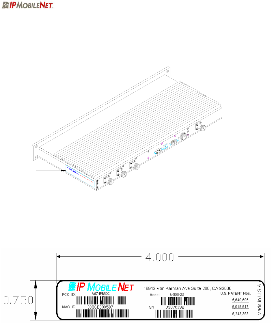
SECTION 3: FCC LABEL.......................................................................................................................... 17
IP8B Base Station FCC Label Placement .................................................................................. 17
IP8B Base Station FCC Label ..................................................................................................... 17
APPENDIX A: IP8B CIRCUIT BOARD DIAGRAM.................................................................................... 18
APPENDIX B: IP8B TEST DATA SHEET.................................................................................................. 22
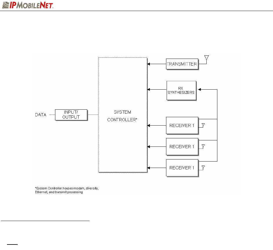
SECTION 1: THEORY OF OPERATION
369548.DOC Page 3
GENERAL BLOCK DIAGRAM
General Block Diagram Definitions
For increased data security, the modem supports the U.S. Government developed Digital Encryption
Standard (DES) data encryption and decryption protocols. This capability requires installation of third-
party IP compliant DES encryption and decryption software.
The standard IPSeries base station circuit board contains five (5) main sections defined below:
Input/Output Circuitry associated with one of the following base station’s data
connectors:
RS232 Serial Port DB9 Data Connector
RJ45 Ethernet 10 Base T Interface Connection
System Controller Houses the modem, diversity, and Ethernet circuitry. Manages the
operation of the base station’s modem providing transmit timeout
protection in the event a fault causes the base station to become
halted in the transmit mode. The system controller also handles the
loading of selected transmit and receive frequencies into the injection
synthesizer. Includes memory for storage through Electrically
Erasable Programmable Read Only Memory (EEPROM) of the base
station’s operating parameters, which are retained after the base
stations power is cycled off.

SECTION 1: THEORY OF OPERATION
369548.DOC Page 4
Modems Convert data into an analog audio waveform for transmission and
analog audio from the receiver to serial data interface. There is one
(1) modem that is dedicated to the transmit operation and two (2)
modems dedicated to the receive operation. The modem dedicated
to the transmit supports a 115.2 KBPS data transmission rate on the
serial port, SLIP protocol, and 19.2 KBPS and 32 KPBS over-the-air
data transmission rate. Provides Forward Error Correction (FEC)
and Error Detection (CRC), bit interleaving for more robust data
communications, and third generation collision detection and
correction capabilities.
Diversity Reception Circuitry selects one of three (3) diversity receiver audio outputs for
processing by the modem by comparing the Received Signal
Strength Indication (RSSI) output from each receiver. Audio from the
receiver with the highest RSSI value is passed to the modems.
RX Injection The Injection Synthesizer board provides a highly stable local
oscillator signal for the three (3) receivers. This displays a serial
data input/output interface, synthesizer, and VCO.
Transmitter Consists of an exciter and a power amplifier module covering various
frequency bands in segments. A different power amplifier module is
required for each segment. The transmitter power control is included
with the power supply circuitry on the same board.
Receiver 1/Receiver 2/ Uses three (3) discrete receivers tuned to the same frequency.
Receiver 3 The three (3) receivers are required to support IPMobileNet’s base
station Diversity Reception System (DRS).
NOTE: Some installations use only two (2) receivers.
The receivers are double-conversion superhetrodynes with an
Intermediate Frequency (IF) of 45 MHz. Each receiver consist of
bandpass filters, RF amplifiers, a mixer, 45 MHz crystal filter, and a
one-chip IF system. The injection synthesizer provides the first local
oscillator signal and outputs from each receiver including RSSI and
analog audio for Diversity Reception.
Power Supply Power supply circuitry derives the various operating voltages
required by the base station. Fixed voltage regulators are employed
through the base station for this purpose.

SECTION 1: THEORY OF OPERATION
369548.DOC Page 5
IP8B Base Station Section Descriptions
System Controller (refer to schematic on page 26)
This section displays the Central Processing Unit (CPU)(U1), clock, and power-on reset circuitry. It
provides more processing power than required for future capabilities to be incorporated without changing
processors. Such capabilities include data encryption/decryption (DES) and remote fault monitoring. U1
features a 16-bit address bus and 128K of internal flash random access memory (RAM).
NOTE: To enter the programming mode it is necessary to reset the switch (S1) and power up again.
CPU operations are controlled by Y3 an 18.432 MHz clock module. Capacitor (C1) and an internal
Schmidt trigger circuit inside of U1 generates the power on reset signal. The RESET* output from U1
drives a latch and decoder found elsewhere on the board.
This section displays the RAM, decoder, EEPROM, and programming power supply circuitry. U2 is a
512K x 8 bit static RAM chip, which provides temporary storage of base station configuration data while
the power is on. This is necessary in order to program the base station. U2 is controlled directly by the
address, data, and control busses from the CPU.
Chip U5 decodes the A11-A14 address bus to provide chip selects for the modem and EEPROM
memory. Chip U6 is an 8-bit latch. It latches inputs from the D0-D7 bus and lights the front panel status
indicators (TX, CD, RX1, RX2, and RX3).
Chip U3 is a serial EEPROM, which provides 2K bits of pre-programmed data storage for the CPU. Data
is clocked out of U3 by EECLK, and back into the CPU via EEDATA.
A programming power supply is required for the flash RAM inside of the CPU, and this function is
performed by U4. This chip is a low dropout voltage regulator with a shutdown control. Resistors R22
and R21 set the output voltage. When the base station configuration data is to be stored in flash RAM,
the CPU makes VPP_ENABLE high. This turns on the regulator, producing a 12-volt output via VPP for
the flash RAM.
This section displays a dedicated processor and voltage regulator. Chip U7 is a processor, which permits
manual keyboard operation of the base station. Regulator VR2 provides 5 volts DC power for all logic
circuitry on the System Controller Board.
Input/Output (refer to schematic on page 30)
This section displays the CPU input/output circuitry. Chip U8 is an RS232 transceiver, which interfaces
the CPU to the modem via J1. From there, the RS232 data goes directly to a rear panel DB9 connector.
U8 converts 5-volt logic-level data to +/-12 volt data in RS232C form, and vice-versa. A charge pump
power supply on the chip converts the +5 volt DC power to the +/-12 volt levels required. The charge
pump uses capacitors (C28 to C31) to generate voltages.
NOTE: The RS232 serial port data transmission rate of the base station is 115.2 KBPS.
Modem Switching
This section displays the connector wiring and modem switching circuitry. Connector J7 is routed to the
front-panel TX, CD, and RX1-RX3 LED indicators. The base station will also accept modulation from an
external source (modem or amplified microphone audio). Transmission gate U10A switches this signal
source.

SECTION 1: THEORY OF OPERATION
369548.DOC Page 6
Modem (refer to schematic on page 29)
This base station uses separate modems for receive and transmit functions so that full-duplex operation
may be obtained. The A0-A1 address bus in addition to the individual read (RD*), write (WR*), and chip
select (MODEMTXCS*) lines control all three (3) modems. Modem operations are timed by Y2, a 4.9152
MHz clock module.
Modem chip U14 is dedicated to the transmit operation. Data from the D0-D7 bus is read by the chip,
and then converted to a 4-level FSK analog signal, which appears on the TXOUT pin. Op amp U21B
buffers the signal, which becomes the MODEM_TXMOD output. From this point, the signal is routed to
the modulation circuitry on the Exciter Board.
Chip U14 has the ability to demodulate receiver audio, although this capability is not used in most
systems. Incoming data-bearing audio from the Diversity Reception circuitry (and selected receiver)
appears at DISC_AUDIO. The signal passes through resistor R54 and into the modem chip. Resistor
R52 and capacitor C41 serve as feedback elements, limiting both the gain and bandwidth of an amplifier
within U14. The modem chip demodulates the audio into 8-bits of data, which exit U14 on the D0-D7 bus.
Chip U14 also provides a bias voltage for the analog circuitry on the Exciter Board. This voltage is about
2.5 volts DC, and it appears on the VBIAS line. The purpose of VBIAS is to bias the Exciter Board analog
circuitry for proper operation. Please note that if this voltage is low or missing, the Exciter Board circuitry
may not work.
Modem chip U15 is dedicated to the receive operation. Incoming data-bearing audio from the Diversity
Reception circuitry (and selected receiver) appears at DISC_ AUDIO. The signal passes through resistor
R56 and into the modem chip. Resistor R55 and capacitor C46 serve as feedback elements, limiting both
the gain and bandwidth of an amplifier within U15. The modem chip breaks down the audio into 8 bits of
data, which exit U15 on the D0-D7 bus.
Modem chip U16 is also dedicated to the receive operation, although it may not be used in this
application. The operation of U16 is exactly the same as U15.
Receive Signal Strength Indication Comparator (refer to schematic on pages 32 & 33)
This section displays the RSSI comparator circuitry. A series of comparators (U20BCD) simultaneous
compare RSSI1 to RSSI2, RSSI2 to RSSI3, and RSSI1 to RSSI3. Within this process eight (8) possible
results are then forwarded by the comparators to a series of NAND gates (U18ABC), which reduce the
number of results to three (3) and translates the results for an analog multiplexer (U19A). To determine
which of the three (3) results is the strongest, the following needs to occur:
For Receiver 1 to be selected as the strongest signal, both input pins on the NAND gate (U18D) must
go high (driving pin 7 of U19A). If Receiver 1 has the strongest signal, a light emitting diode
(LED)(D1) lights indicating Receiver 1 was selected.
For Receiver 2 to be selected as the strongest signal, the inverter (U17B) must go high (driving pin 6
of U19A). If Receiver 2 has the strongest signal, D2 lights indicating Receiver 2 was selected.
For Receiver 3 to be selected the strongest signal, the inverter (U17C) must go high (driving pin 5 of
U19A). If Receiver 3 has the strongest signal, D3 lights indicating Receiver 3 was selected.
SEL_RSSI is the output selected with the strongest signal. When RSSI voltage exceeds a threshold,
another LED (D4) lights. As the other three (3) LEDs, this circuit is intended as a diagnostic tool. It
provides a go/no go indication that an RF signal has been received. A pot (R74) sets the turn-on voltage.

SECTION 1: THEORY OF OPERATION
369548.DOC Page 7
Baseband (refer to schematic on page 34)
This circuitry amplifies the audio from each receiver, routes it through a RF multiplexer, and selects the
audio from the receiver with the highest RSSI value. The comparator circuit on the previous sheet
controls it.
There are three (3) channels of audio, with separate gain and DC offset adjustments to compensate for
performance differences in the receivers. For example, incoming audio from receiver 1 appears at
AUDIO 1. An op amp (U12D) is then amplifies the audio. A pot (R72) adjusts the gain, while another pot
(R57) adjusts the DC offset on the output. The amplifier output passes through a RF multiplexer (U19B),
then drives a low pass filter (U9) through another op amp (U12A) and through the AUDIO_OUT line,
which goes to a switch (S3) and to pin 4 of a connector (J3).
The remaining audio circuits work in the same manner.
The output from U19B also appears on DISC_AUDIO, which goes to the CPU (U1) and from there the
audio is demodulated by the modems.
Receiver Board (refer to schematic on page 44)
Please be aware that the base station uses three (3) identical receiver boards. As a result, the circuitry
will be described only once.
Front end. Incoming signals pass through a bandpass filter (FLT1). The desired signals are amplified by
U4 and additional selectivity is provided by a SAW filter (FLT2). The signal passes through an IC mixer
(U5) and the output passes through two (2) crystal filters (FLT3 and FLT4).
IF Amplifier (refer to schematic on page 45)
The incoming 45 MHz signal passes through C15, C17, and R12 which provides impedance matching to
the IF amplifier input. U2 is a super heterodyne IF subsystem. Inside the chip, the signal is applied to a
mixer. The mixer also accepts a 44.545 MHz local oscillator input. The local oscillator consists of an
internal amplifier, plus crystal (Y1) and associated components. The mixer output passes through Y4, a
455 KHz ceramic IF filter. It is amplified, passed through another 455 KHz ceramic filter (Y3), and on to a
second IF stage. The IF output drives a quadrature detector. The phase shift elements for the detector
are C8 and Y5. The recovered audio appears at pin 9, while RSSI appears at pin 7.
Within the RSSI circuitry, chip U2 uses a detector, which converts the AGC voltage generated inside the
chip into a DC level corresponding logarithmically to signal strength. RSSI is used by Diversity Reception
on the System Controller to select the receiver with the highest quality signal.
A filter consisting of a resistor (R8) and a capacitor (C18) provides high frequency de-emphasis for the
audio. The audio is buffered by op amp U1A. From there the AUDIO output line goes to a connector, for
hookup to Diversity Reception on the System Controller Board.
Resistor (R9) and capacitor (C10) provides RF filtering for the DC RSSI voltage. The RSSI is buffered by
op amp U1B. From there the RSSI output line goes to a connector, for hookup to Diversity Reception on
the System Controller Board.
Several sets of 455 KHz IF filters (Y4 and Y3) are available to suit receiver selectivity requirements.
Should replacement of these filters be required, exact replacement parts must be used.

SECTION 1: THEORY OF OPERATION
369548.DOC Page 8
Receiver Injection (refer to schematic on page 20 & 21)
This displays a serial data input/output interface, synthesizer, and VCO. The I/O interface circuitry
accepts clock, serial data, and enable signals from the System Controller Board via terminal block TB1. A
lock detect (LD) status output is returned to the System Controller Board from the synthesizer. U6 is a
hex Schmidt Trigger inverter, which squares up incoming signals for reliable operation of the synthesizer
chip. This is necessary because of a cable run between the two (2) boards.
The main section of this board is synthesizer chip (U5). The device contains the key components of a
phase locked loop (PLL), including a 1.1 GHz prescaler, programmable divider, and phase detector. In
operation, the desired frequency is loaded into U5 as a clocked serial bit stream via the CLK and DATA/I
inputs. The lock detection circuitry consists of inverters U6E/U6F, diode CR1, and resistor R3. When the
synthesizer is in lock, the LD pin on U5 is high, making the LD output on terminal block TB1 high.
The UHF injection signal is generated by module VCO1. This device is a wide-range voltage controlled
oscillator (VCO). A voltage on the C input determines the VCO frequency. The voltage is generated by
the phase detector output (PD/O) of U5, which drives a loop filter consisting of R2, C23, C7, R5, C15, and
C16. The filter integrates the pulses, which normally appear on PD/O into a smooth DC control signal for
the VCO. The output of VCO1 is attenuated by module AT1, resulting in improved VCO stability.
Reference module (Y1) provides a high-stability 10 MHz reference frequency. Y1 is a voltage controlled,
temperature controlled crystal oscillator (VCTCXO). This device also has a VC input which accepts a
control voltage from pot R7. The pot permits a slight shift in the reference frequency which enables the
three (3) receivers to be tuned precisely to the assigned receive frequency. A diode (CR2) provides
additional voltage regulation, improving the frequency stability of reference Y1.
The RF output circuitry consists of RF amplifier (U4), and two-way power splitters (U3, U1, and U2). U4
increases the signal level to correct for losses in the splitters. The splitter U3 provides two (2) RF outputs.
One output drives splitter U1, which provides local oscillator injection for receivers 2 and 3. The other
output drives splitter (U2), which drives receiver 1 and the PLL_FEEDBACK input on chip U5.
Exciter Board (refer to schematic on page 49)
This section displays the input/output interface, transmitter keying, and power supply circuitry. The
input/output interface is built around terminal block (TB1) and Schmidt Trigger inverters (U4). Incoming
clock, serial data, and chip select signals on block TB1 are squared up by U4. Then they are sent to the
appropriate inputs on the low pass Bessel filter (U2). The EXCDATA source comes from the receive
synthesizer on the Injection Synthesizer Board. A Schmidt Trigger chip is used here because of a cable
ran to the System Controller Board. The synthesizer returns a lock detect output to the Injection
Synthesizer Board via U4D and EXCLD.
A regulator (VR3) powers the T/R switch circuitry. When the System Controller Board makes TXKEY*
low, turning on transistor Q4 and FET Q1. This applies 5-volt power to the TXENABLE output, turning on
the T/R switch on the Power Amplifier Board. At the same time, transistor Q2 conducts, grounding the
KEY* input of the Power Amplifier Board. Finally, inverter U4E goes high and turns on RF switch U5,
connecting the VCO output to the Power Amplifier Board for transmission.
The power supply consists of two (2) voltage regulators. A regulator (VR1) provides 9-volt power for the
VCO. Another regulator (VR2) provides low noise 5-volt power for the logic circuitry, synthesizer chip,
and analog circuitry.

SECTION 1: THEORY OF OPERATION
369548.DOC Page 9
Analog Modulation (refer to schematic on page 52)
This section displays the analog modulation circuitry. Incoming modem audio from the System Controller
Board appears at TXMOD, and is buffered by op amp U3A. If an external modulation source (modem or
amplified microphone) is connected to the base station’s DB9 connector, audio appears at EXTMOD.
From there the audio passes through low pass Bessel filter U2. The audio is inverted and amplified by an
op amp (U3B). It then passes on to the VCO module via VCOMOD. Pot R11 adjusts the level to suit the
VCO.
The 10 MHz reference is also modulated in order to counteract the corrective effects of the synthesizer
loop circuitry. For example, if only the VCO were modulated, the synthesizer would try to compensate for
the frequency “error,” caused by the modulation. This effectively reduces the amount of modulation
available. Modulating the reference and the VCO simultaneously deceives the loop into not
compensating for the modulation, because when the reference frequency goes high, the VCO frequency
goes high, and vice-versa.
An op amp (U1A) amplifies the AUDIO output from another op amp (U3D) and applies it to jumper block
JP1. Pot R4 adjusts the gain of U1A. Op amp (U1B) inverts the phase of the audio and applies it to the
other side of jumper block JP1. The purpose of the jumper block is to select the proper phase of the
audio. If the wrong phase is used, on modulation peaks the reference will swing in the same direction as
the VCO, canceling out most of the modulation. The output from the jumper block goes to the 10 MHz
reference via REFMOD.
The VBIAS input is a 2.5-volt DC source, which biases the op amps to the correct operating point. It is
generated by modem chip (U14) on the System Controller Board.
Phase Locked Loop (refer to schematic on page 53)
This section displays phase locked loop (PLL) circuitry. The 10-MHz reference (Y1), runs synthesizer
(U6), which in turn controls VCO VCO1. The main section of this board is the synthesizer chip (U6). The
device contains the key components of a PLL, including a 1.1 GHz prescaler, programmable divider, and
phase detector.
In operation, the desired frequency is loaded into U6 as a clocked serial bit stream via the CLK and DATA
inputs. The lock detection circuitry consists of inverters U4D, diode CR1, and resistor R28. When the
synthesizer is in lock, the LD pin on U6 is high, making the EXCLD output on terminal block (TB1) high.
The EXCLD output on TB1 routes the lock detect output from the Exciter Board. This configuration tells
the CPU on the System Controller Board that it is acceptable to process received data, or to key the
transmitter when LD is high. Otherwise, if a fault in either synthesizer prevents a lock, receive and
transmit operation will be inhibited.
The switch (JP1) is used to select the supply voltage to chip U6. The UHF injection signal is generated
by module VCO1. This device is a wide-range voltage controlled oscillator (VCO). A voltage on the VT
input determines the VCO frequency. The voltage is generated by the phase detector output (PD/O) of
U2, which drives a loop filter consisting of R31, C50, C28, and C25. The filter integrates the pulses,
which normally appear on PDOUT into a smooth DC control signal for the VCO. The output of VCO1 is
attenuated by module AT1, resulting in improved VCO stability.
RF amplifier U8 amplifies the signal and applies it to a two-way power splitter (U7). One output of U7 is
connected to a switch (U5). U5 is enabled by signal TX when the transmitter is enabled. The other
output of the splitter provides feedback to U6.

SECTION 1: THEORY OF OPERATION
369548.DOC Page 10
Power Amplifier (refer to schematic on page 40)
The transmit injection signal from the RF injection section is applied to the high-powered linear amplifier
(U1) one (1) watt amplifier. The signal is then routed to the final power amplifier boosting the output
signal to 20 watts.

SECTION 2: FACTORY TEST PROCEDURE
369548.DOC Page 11
Equipment List
The following table lists the equipment required to perform the IP8B Base Station Factory Test
Procedure.
CHECKLIST OF REQUIRED MATERIAL FOR
PRELIMINARY TESTING OF THE IPSeries BASE STATION
NO. REQUIRED TOOLS ;
1
Calibrated Base Station System – Consisting of the following components:
(1) Appropriate version IPSeries Base Station to be tested
(2) Desktop or laptop computer configured as an Internet Protocol Network Controller (IPNC)
(3) Corresponding IPSeries Mobile radio (If an IP8B base station, use IP8 mobile radio)
(4) Desktop or laptop computer with two (2) available serial ports and Microsoft Windows 95 or
greater and IPMobileNet Dial-Up Networking, IPMessage software (SLIP2IPMN.exe), and
HyperTerminal for base station installed
2 Comm Test Set (HP 8920A or B)
3 High Frequency Probe (85024A)
4 Power Supply for 85024A Probe (HP1122A)
5 Four (4) Channel Scope (Tektronix TDS 460A)
6 General Purpose Scope Probe
7 Digital multi-meter Tektronix Fluke (DMM912 77)
8 DC power supply with ammeter, 13.8V, 12 amps or more (Astron VS12M or equivalent)
9 100-watt dummy load/attenuator (Pasternack PE7021-40 or equivalent)
10 Four (4) antennas (generic mag mounts) tuned to frequency or transceiver
11 Serial cable DB9M – DB9F connectors (generic)
12 Input/Output (I/O) Board (IPMN p/n: 502-80081)
13 IPSeries Base Station power cable specified for use with the specific base station being used
14 Three (3) serial DB9F-DB9M Null Modem cables

SECTION 2: FACTORY TEST PROCEDURE
369548.DOC Page 12
Programming and Configuring the Base Station
This section applies to the 851-866 frequency range of the IPSeries Base Station. Important! The base
station’s IP address must be known prior to performing the procedures in this section.
The programming procedure should be performed when it is necessary to upgrade a base station’s
Firmware or to change the operating parameters to suit client needs.
Viewing the Base Station’s Configuration Data
Step 1 At the HyperTerminal window, type in the appropriate password and press [ENTER].
Step 2 Type ? and press [ENTER]. The following example displays in the HyperTerminal
window:
Host serial = 115200,N,8,1, timeout=200
Host framing = SLIP, no split frames no status messages
tunnel = 0
TX format = new
Injection = LOW SIDE, 45MHz
channel spacing = 25000
Channel = 0
Channel Tx freq Rx freq Inj freq
Frequency=0 , 815.100000, 860.100000, 815.100000
Serial number: yyyyyyyyy
RIM address = 1
Frequency group = 1
TX quiet time = 5
Symbol sync time = 12 milliseconds, 0 extra inter-split-frame count
TX tail time = 5
Radio data rate = 19200
Max data tx time = 60 seconds
Carrier detect delay time = 1 millisecond
Station ID = ABC123
Station ID time =10 minutes
Polarity = TX+, RX+
Allow crc errors = 0
Suppress keep alive = 0
Allow base to base = 0
Timeslot status = 0
Duplicate time = 10 milliseconds
Control head grant delay = 50 milliseconds
RIM DD delay = 0 milliseconds
Retry interval = 0 milliseconds
Retry time limit = 0 milliseconds
RSSI step = 25 (=19dBm)
IPNC = 192.168.3.3
SLIP Address = 192.168.4.6
RF IP Address = 192.168.3.1
SNTP interval = 60 seconds
num timeslots = 16
timeslot period = 992ms
timeslots per voice packet = 4
noise = -128dBm
Fixed TX Delay = 0 milliseconds
Scale TX Delay = 0 microseconds

SECTION 2: FACTORY TEST PROCEDURE
369548.DOC Page 13
Adjustment / Alignment Procedures
Make appropriate notations of any items that require attention during this procedure. This information is
needed later during the repair process.
Startup
Step 1 Remove the base station cover placing the screws in a location where they will not be
misplaced.
Step 2 Connect the base station to the appropriate components.
Step 3 Power up the base station and computer. The power supply ammeter must read 1.2
amps or less with a 13.8 VDC input.
Receiver Injection
Step 1 Using the HP high frequency probe verify that the receiver injection frequency is present
at each of the three (3) receivers by monitoring the receivers R24 surface mount pad
which lies on the 50 ohm track between P1 and C43.
Step 2 Adjust R23 on the receiver injection circuit board to set the injection frequency within 10
Hz of the exact injection frequency. The amplitude of the injection frequency should read
approximately +5 dBm ±1 dBm.
Receiver
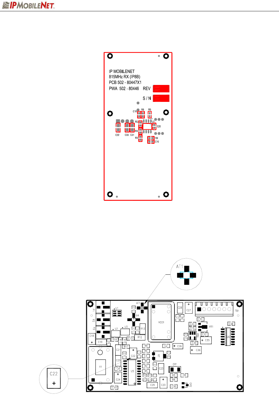
Step 1 Using the high frequency probe, monitor the 44.545 MHz second injection frequency
at U6 pin 3, adjust trimmer capacitor (C22) to the center of the oscillator’s oscillation
range. The amplitude level of pin 3 of U6 should read between +5 and +10 dBm.
Step 2 Inject an on-frequency signal at a level of –80 dBm, modulated with a 1 KHz test tone at
±5.0 KHz deviation into the receiver under test.
Step 3 Check the receiver’s sensitivity, verifying that the SINAD is 12 dB or better at a maximum
level of –119 dBm (-120 is typical).

SECTION 2: FACTORY TEST PROCEDURE
369548.DOC Page 14
Diversity Reception
Step 1 Inject an on-frequency signal at a level equal to Receiver 1 12dB SINAD level, modulated
with a 1 KHz test tone at ±5.0 KHz deviation into Receiver 1.
Step 2 While monitoring TP1 with the digital multi-meter, adjust RSSI1 low adjust potentiometer
(R12) for a reading of 0.750 VDC ±10 mV.
Step 3 Increase the amplitude of the signal by 50 dBm.
Step 4 While monitoring TP1 with the digital multi-meter, adjust RSSI1 high adjust potentiometer
(R11) for a reading of 2.75 VDC ±10 mV.
Adjustments R11 and R12 are interactive adjustments, therefore continue adjustments until the DC voltage
at TP1 is 0.750 VDC for the receiver’s 12 dB SINAD level and 2.75 VDC for a 50 dBm increase from the
receiver’s 12 dB SINAD level.
Step 5 Inject an on-frequency signal at a level equal to Receiver 2 12dB SINAD level, modulated
with a 1 KHz test tone at ±5.0 KHz deviation into Receiver 2.
Step 6 While monitoring TP2 with the digital multi-meter, adjust RSSI1 low adjust potentiometer
(R10) for a reading of 0.750 VDC ±10 mV.
Step 7 Increase the amplitude of the signal by 50 dBm.
Step 8 While monitoring TP2 with the digital multi-meter, adjust RSSI1 high adjust potentiometer
(R9) for a reading of 2.75 VDC ±10 mV.
Adjustments R9 and R10 are interactive adjustments, therefore continue adjustments until the DC voltage
at TP2 is 0.750 VDC for the receiver’s 12 dB SINAD level and 2.75 VDC for a 50 dBm increase from the
receiver’s 12 dB SINAD level.
Step 9 Inject an on-frequency signal at a level equal to Receiver 3 12dB SINAD level, modulated
with a 1 KHz test tone at ±5.0 KHz deviation into Receiver 3.
Step 10 While monitoring TP3 with the digital multi-meter, adjust RSSI1 low adjust potentiometer
(R33) for a reading of 0.750 VDC ±10 mV.
Step 11 Increase the amplitude of the signal by 50 dBm.
Step 12 While monitoring TP3 with the digital multi-meter, adjust RSSI1 high adjust potentiometer
(R35) for a reading of 2.75 VDC ±10 mV.
Adjustments R33 and R35 are interactive adjustments, therefore continue adjustments until the DC voltage
at TP3 is 0.750 VDC for the receiver’s 12 dB SINAD level and 2.75 VDC for a 50 dBm increase from the
receiver’s 12 dB SINAD level.

SECTION 2: FACTORY TEST PROCEDURE
369548.DOC Page 15
Step 13 Inject on-frequency signal at a level of –80 dBm, modulated with a 1 KHz test tone at
±5.0 KHz deviation into Receiver 1.
Step 14 While monitoring the AC voltage at TP6 adjust audio 1 AC adjustment potentiometer
(R72) for 350 mVRMS (±1 mV).
Step 15 While monitoring the DC voltage at TP6 adjust audio 1 DC adjustment potentiometer
(R57) for 2.500 VDC (±1 mV).
The audio AC and DC adjustments are interactive, therefore continue adjusting R72 for 350 mVRMS and
R57 for 2.500 VDC until further adjustments are no longer required.
Step 16 Inject on-frequency signal at a level of –80 dBm, modulated with a 1 KHz test tone at
±5.0 KHz deviation into Receiver 2.
Step 17 While monitoring the AC voltage at TP6 adjust audio 1 AC adjustment potentiometer
(R71) for 350 mVRMS (±1 mV).
Step 18 While monitoring the DC voltage at TP6 adjust audio 1 DC adjustment potentiometer
(R58) for 2.500 VDC (±1 mV).
The audio AC and DC adjustments are interactive, therefore continue adjusting R71 for 350 mVRMS and
R58 for 2.500 VDC until further adjustments are no longer required.
Step 19 Inject on-frequency signal at a level of –80 dBm, modulated with a 1 KHz test tone at
±5.0 KHz deviation into Receiver 3.
Step 20 While monitoring the AC voltage at TP6 adjust audio 1 AC adjustment potentiometer
(R53) for 350 mVRMS (±1 mV).
Step 21 While monitoring the DC voltage at TP6 adjust audio 1 DC adjustment potentiometer
(R59) for 2.500 VDC (±1 mV).
The audio AC and DC adjustments are interactive, therefore continue adjusting R53 for 350 mVRMS and
R59 for 2.500 VDC until further adjustments are no longer required.
Step 22 Adjust the carrier detect potentiometer (R74) to illuminate a level of –116 dBm.
Receive Data
Step 1 Using a calibrated mobile radio, generate uplink data messages using the X=1400,19
command in the IPMessage Utility program.
Step 2 Attach an antenna to one of the base station’s receiver ports and verify on the base
station monitor screen (HyperTerminal) that the received message data quality are
consistently 240 and higher for 1400 character messages. Repeat test for each receiver.

SECTION 2: FACTORY TEST PROCEDURE
369548.DOC Page 16
Exciter
Step 1 Using the X=1400,19 command, generate data messages so the transmit power and
frequency can be checked.
Step 2 Note the power level and then on the power amplifier circuit board adjust the
potentiometer (R3) fully counterclockwise (this will enable low power transmit operation).
Step 3 Connect the base stations’ transmit port to the HP communication test set.
Step 4 While transmitting data messages using the X=1400,19 command, adjust the following:
TCXO Y1 for minimum frequency error
R42 for ±5 KHz deviation
Transmit output power should be approximately 1mWatt. The REFMOD adjustment needs to be made
while the base station is transmitting real data messages to and from a mobile radio. This is most easily
done using the ping command to ping the IPNC from a mobile radio. This will cause the base station to
repeatedly send data messages and will facilitate the REFMOD adjustment.
Step 5 Connect the base station to the IPNC.
Step 6 Using a calibrated mobile radio operating on the base station’s channel, adjust R30 for
consistent data quality readings of 248 (as observed on the mobile radio’s attached PC
IPMessage window). Access the MSDOS prompt and ping using the following command:
>;ping 192.168.3.3 –t –l 500 –w 2000
This command will ping the IPNC continuously with a 500-character test message. Press [Ctrl]+C to
stop the ping.
Power Amplifier
Step 1 Connect the base station’s transmit port to the communication test set.
Step 2 Using the X=1400,19 command, generate data messages.
Step 3 Slowly increase the base station output power by turning the power control potentiometer
clockwise until the power noted in Step 2.
Do not exceed 20 watts output power, as this will reduce the life of the amplifier module. If the base
station uses a power amplifier, output power must be set to achieve power output specified for the
specific base station installation.
Step 4 Perform a close visual inspection of the base station paying close attention to
manufacturing related problems such as loose screws, solder practices, etc.
SECTION 3: FCC LABEL
369548.DOC Page 17
IP8B Base Station FCC Label Placement
LABEL
IP8B Base Station FCC Label
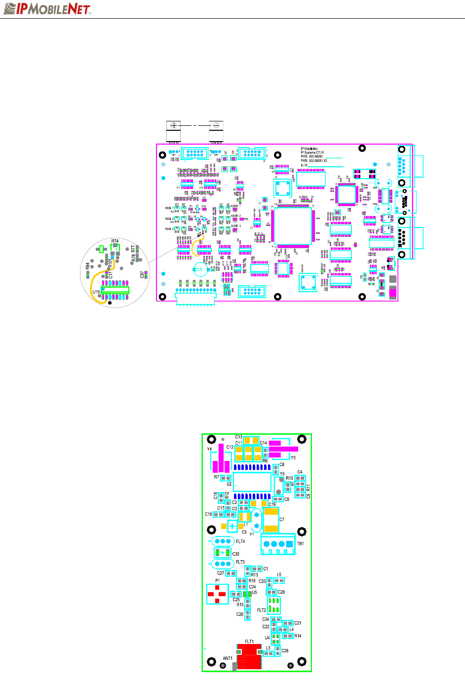
APPENDIX A: CIRCUIT BOARD DIAGRAMS
369548.DOC Page 18
System Controller
Receiver - Top
C90
R41
R42
R43
C89
J7
1
VR3
J8
R44
1
R82
R81
+
U19
D7
U18
U14
TP5
U10
C83
51
C56
50
16
R62
C84
75
76
32
U4
U16
U15
C8
C7
R31
ADD JUMPER (30 AWG INSULATED WIRE)
73
U7
72
REWORK INSTRUCTION
R33
TP4
TP8
F1
S1
26 100 R80
R65
R66
R79
C88
10
9
7
U21
8
U6
2
1
J5
U17
Y2
U2
109
108
from U19 Pin2 to VIA (RVCC)
R83
R40
12
R39 C58
R88
C59
U20
J3
25 1
Y1
U13
C76
J2
R50
C28
S2
S3
U8
J1
C77
R51
C75
T1
C74
++
APPENDIX A: CIRCUIT BOARD DIAGRAMS
369548.DOC Page 19
Receiver – Bottom
Receiver Injection
INSTALL C22 AS SHOWN
THESE PADS (SIZE 0805)
ADD 1000pF ACCROSS
APPENDIX A: CIRCUIT BOARD DIAGRAMS
369548.DOC Page 20
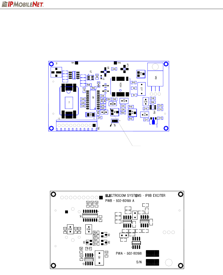
Exciter – Top
Exciter – Bottom
C44 C37
R30
C27
R34
R35
C46
+
+
++
C36
U5
+
+
+
+
C50 POLARITY
C35
C29
+
+
+
R5
U1
R13
R8
R7
C5
C7
U3
R12 R3
C6
R6
C1
U2
R9 C4
C2
R17
C3
APPENDIX A: CIRCUIT BOARD DIAGRAMS
369548.DOC Page 21
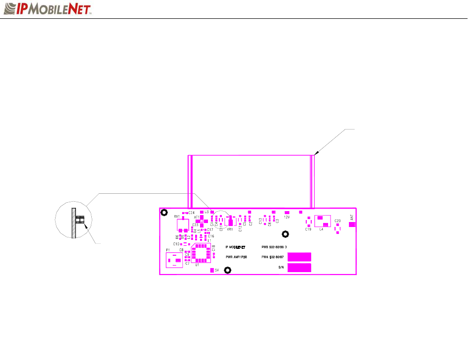
Power Amplifier
U3
FOR REF ONLY
ON TOP OF C11
C14 TO BE MOUNTED
C11
C14

APPENDIX B: IP8B TEST DATA SHEET
369548.DOC Page 22
Program and Configure the Base Station
Date
Serial Number
Firmware Revision
End User
Tester
Adjustment / Alignment Procedures
Receiver Injection
Parameter Spec Measured
Injection Frequency Error at RXINJ1(within +/- 10
Hz of exact injection frequency) +/- 100 Hz
P1 & C39 5 +/- 1 dBm
Receiver Diversity Reception Controller 1, 2 & 3
Parameter Spec Receiver 1
Measured
Receiver 2
Measured
Receiver 3
Measured
U2 Pin 4 +10 to +5 dBm
RSSI Test Point TB1-4 2.8 to 3.0 VDC
Distortion
(1 kHz Test Tone @ 5.0 kHz) 3%<
SINAD 12 dB
(1 kHz Test Tone @ 5 kHz) -119dBm >
Audio AC Amplitude
(1 kHz Test Tone @ 5 kHz
Deviation)
350 mVRMS
+/- 1mV
Audio DC Amplitude
(1 kHz Test Tone @ 5 kHz
Deviation)
2.5 VDC
+/1 1mV
Carrier Detect Light Set -116 dBm

APPENDIX B: IP8B TEST DATA SHEET
369548.DOC Page 23
Data Quality
Parameter Spec Measured
Receiver 1 Data Quality
(x=1400, 19 Command IPMessage Utility) 240>
Receiver 2 Data Quality
(x=1400, 19 Command IPMessage Utility) 240>
Receiver 3 Data Quality
(x=1400, 19 Command IPMessage Utility) 240>
Exciter
Parameter Spec Measured
Transmit Frequency Error
(Transmitting 1400 character test message) +/- 500 Hz
Transmit Modulation Deviation
(5.3 kHz while transmitting 1400 character test
message)
5.1 kHz to 5.3 kHz
Transmit Data Quality
(While transmitting 1400 character test message
to the base station)
240>
Transmit Power Control
Warning: Do Not exceed 20 Watts RF output power during this test
Parameter Spec RF Out RF Out Max Level set to
Output Power
(Use x=1400,19 command) 20 +/- 1 Watt
Test Check List
Test Task Completed
(9)
Attached copy of Base Station’s Firmware Settings
Visual Inspection
Copy Base Station Settings Below: