IRay Technology 01070189 WiFi Module User Manual
iRay Technology Co. Ltd. WiFi Module Users Manual
Contents
Users Manual
AI-Link
WIFI-V897 Series
IEEE 802.11 2X2 MIMO ac/a/b/g/n WiFi
Features:
➢ Reserving System
IEEE Std. 802.11a
IEEE Std. 802.11b
IEEE Std. 802.11g
IEEE Std. 802.11n
IEEE Std. 802.11ac
➢ Chip Solution
Marvell 88W8897
Model
Standard
Rate
Channel
POWER
WIFI-2-V897EA1
IEEE 802.11a/b/g/n/ac
866.7Mbps
2.4G/5G
5V
Sichuan AI-Link Technology Co.,Ltd
Add: Anzhou,Industrial park,Mianyang,Sichuan,China
Fax : +86-0816-2416943
http://www.changhong.com
WIFI-2-V897EA1
IEEE 802.11a/b/g/n/ac 2T2R
Sichuan AI-Link Technology Co., Ltd. page 2 of 23
Record of Modification
Feedback of customer’s Confirmation
We accept the specification after Confirmed
Customer name
Customer signature
Confirmation Date
Please feed back this paper and first paper after your signature by the address,thanks!
ADD: Anzhou,Industrial park,Mianyang,Sichuan,China
Factory: Sichuan iLink Technology Co.,Ltd.
Approved
Checked
Designed
Product
WiFi Module
Bai lang
Qian zijin
Fan xijun
Model
WIFI-2-V897EA1
Date
2018-05-18

WIFI-2-V897EA1
IEEE 802.11a/b/g/n/ac 2T2R
Sichuan AI-Link Technology Co., Ltd. page 3 of 23
No
Date of
modification
Main content of
modification
Reason of
modification
Serial number of
modification
Confirm
1
20180518
Confirmed for the
first time
Fan xijun
WIFI-2-V897EA1
IEEE 802.11a/b/g/n/ac 2T2R
Sichuan AI-Link Technology Co., Ltd. page 4 of 23
1. Introduction
WIFI-2-V897EA1 is based on Marvell 88W8897,complied with IEEE 802.11a/b/g/n/ac. The Module is a
highly integrated MAC/BBP and 2.4/5GHz RF/PA/LNA single chip which supports a 866.7Mbps PHY
rate. The Module is designed to support standard-based features in the areas of security, quality of
service, and international regulations, giving end users the greatest performance anytime and in any
circumstance. This documentation describes the engineering requirements specification.
■ IEEE802.11ac (draft)compliant,2x2 MIMO spatial stream multiplexing with data rates up to
MCS9(866.7Mbps)
1.1 RF module Overview
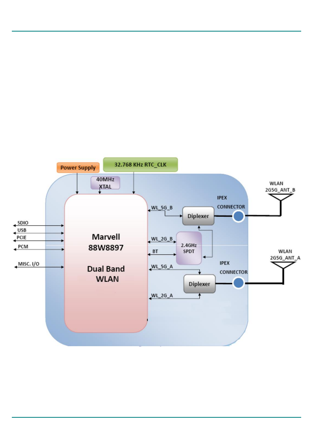
The general HW architecture for the module is shown in Figure 1. This WLAN Module design is based
on Marvell 88W8897. It is a highly integrated single-chip MIMO(Multiple In Multiple Out) Wireless LAN
(WLAN) network interface controller complying with the 802.11ac specification over SDIO,PCIE,USB
and UART interface.. It combines a MAC, a 2T2R capable baseband, and RF in a single chip. The
88w8897 provides a complete solution for a high throughput performance wireless client .
.
Figure 1 WIFI-2-V897EA1 Block Diagram

WIFI-2-V897EA1
IEEE 802.11a/b/g/n/ac 2T2R
Sichuan AI-Link Technology Co., Ltd. page 5 of 23
Note: Interface supports and combinations as shown below:
Scenario
WLAN
Firmware
Download I/F
Firmware
Download
Mode
Configuration
*
1
PCIe
PCIe
Serial
CON[3:0]=b'1
110
NOTE:
PCIe v3.0(2.5Gbps) interface
USB 2.0 interface with LPM support
1.2 Specification reference
This specification is based on additional references listed below.
_ IEEE Std. 802.11a
_ IEEE Std. 802.11b
_ IEEE Std. 802.11g
_ IEEE Std. 802.11n
_ IEEE Std. 802.11ac

WIFI-2-V897EA1
IEEE 802.11a/b/g/n/ac 2T2R
Sichuan AI-Link Technology Co., Ltd. page 6 of 23
1.3 System Functions
Table1: General Specification as below:
Main Chipset
Marvell 88W8897
Operating Frequency
2.4G/5G
WiFi Standard
802.11a/b/g/n/ac(2x2)
Modulation
11b: DBPSK, DQPSK and CCK and DSSS
11a/g: BPSK, QPSK, 16QAM, 64QAM and OFDM
11n: BPSK, QPSK, 16QAM, 64QAM and OFDM
11ac: BPSK, QPSK, 16QAM, 64QAM,256QAM and OFDM
Data rates
11b:1, 2, 5.5 and 11Mbps
11a/g:6, 9, 12, 18, 24, 36, 48 and 54 Mbps
11n: MCS0~15, up to 300Mbps
11ac: MCS0~9, Nss=2, up to 866.7Mbps
Form factor
LGA
Host Interface
PCIE,USB
PCB Stack
6-layers design
Dimension
Typical,30.0mmx 26.8mm
Antenna
External antenna
Operation Temperature
-20℃ to +50℃
Storage Temperature
-20℃ to +50℃
Operation Voltage
DC 3.3V ,
Interfaces
PCIe interfaces support for WLAN
Systems
1、 Drip-in WLAN Linux drivers are Android ready and
validated on Android based systems.
2、Support for Linux kernel versions up to 2.6.32.
WIFI-2-V897EA1
IEEE 802.11a/b/g/n/ac 2T2R
Sichuan AI-Link Technology Co., Ltd. page 7 of 23
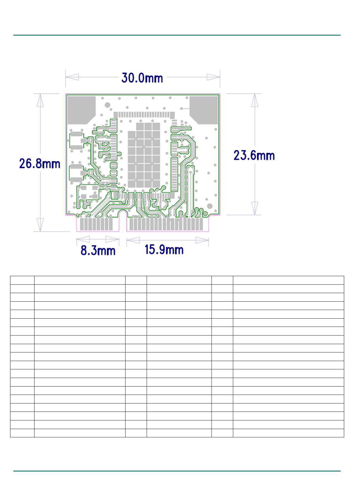
2. Mechanical Specification
Typical Dimension (L x W): 30.0mmx 26.8mm
Pin feet from left to right
PIN
Description
PIN
Description
PIN
Description
1
WAKEn
19
N.C
37
GND
2
VDD33
20
PCIE_DISABLE
38
USB_DP
3
GPIO0/CLK_REQ
21
GND
39
VDD3.3V
4
GND
22
PCIE_PERST
40
GND
5
WLAN_IRQ(O)/WAKE_UP
23
PCIE_TX_N
41
VDD3.3V
6
N.C
24
VDD3.3V
42
N.C
7
PCIE_CLKREQ_N
25
PCIE_TX_P
43
GND
8
N.C
26
GND
44
LED_WLAN
9
GND
27
GND
45
GPIO[10]/NFC_NOT_ALLOWED
10
N.C
28
N.C
46
LED_WPAN
11
PCIE_CLE_N
29
GND
47
GPIO[11]/NFC_ACTIVE
12
N.C
30
N.C
48
N.C
13
PCIE_CLK_P
31
PCIE_RX_N
49
N.C
14
N.C
32
N.C
50
GND
15
GND
33
PCIE_RX_P
51
PDN
16
N.C
34
GND
52
+3.3Vaux
17
N.C
35
GND
18
GND
36
USB_DM
WIFI-2-V897EA1
IEEE 802.11a/b/g/n/ac 2T2R
Sichuan AI-Link Technology Co., Ltd. page 8 of 23
Notes:
1. PCIE Impedance targets: Single-ended Z of 60 ohms +- 15% . Differential
Impedance of ~100 ohm +- 20%.
2. USB Impedance targets: D+/D- are differential and should have 90ohms
impedance.
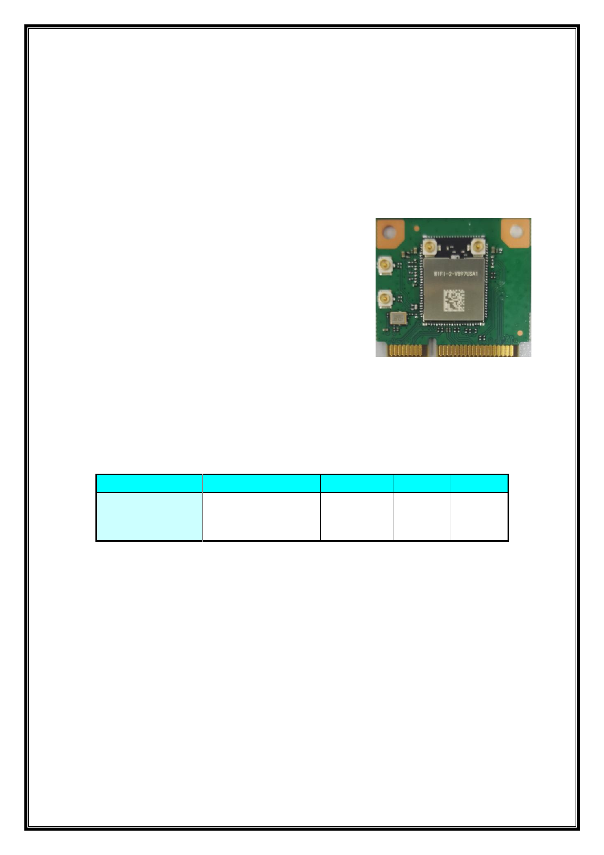
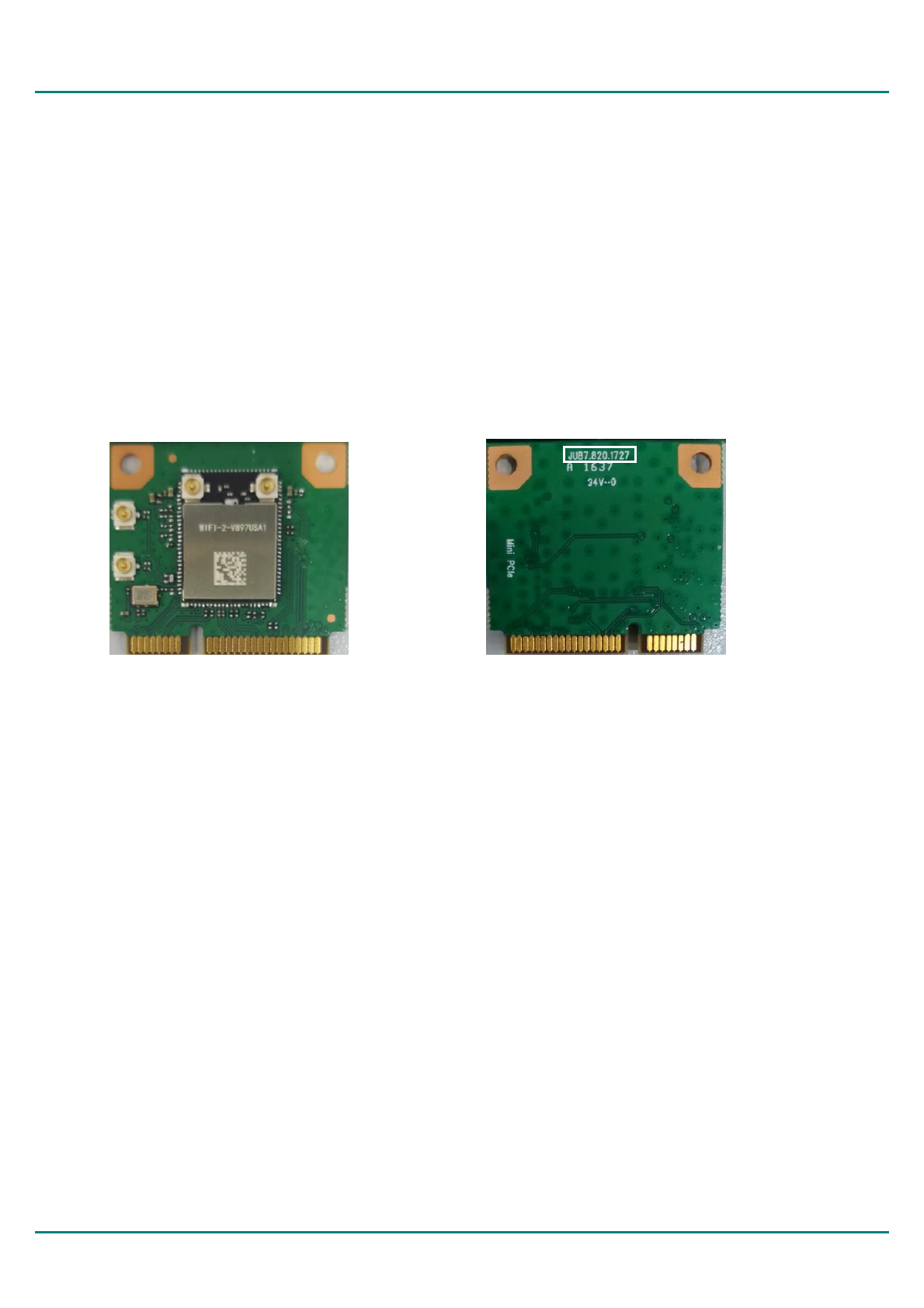
3. Product Picture
TOP VIEW BOTTOM VIEW
WIFI-2-V897EA1
IEEE 802.11a/b/g/n/ac 2T2R
Sichuan AI-Link Technology Co., Ltd. page 9 of 23
4. Electrical Specification
This Specification is based-on conductive DVT testing result. The extreme condition include overall
temperature (-20℃,+25℃,+50℃) and overall voltage (3.3V +/-15% ,).
4. 1 Absolute Maximum Ratings:
Symbol
Parameter
Min.
Typ.
Max.
Unit
Remarks
Pin73/ VIO
Host I/O power supply
-
-
-
1.8
2.5
3.3
2.2
3.0
4.0
V
Pin44/ VIO_SD
SDIO power supply
-
-
1.8
3.3
2.2
4.0
V
Pin5/ 3V3_VBAT
LDO VBAT input
-
3.3
4.0
V
Pin72/ 3V3_USB
LDO USB VBAT input
-
3.3
4.0
V
Pin4/ 3V3_RF
LDO RF VBAT input
-
3.3
4.0
V
4. 2 Recommended Operating Conditions:
Symbol
Parameter
Min.
Typ.
Max.
Unit
Remarks
Pin73/ VIO
1.8V/2.5V/3.3V digital
I/O power supply
1.62
2.25
2.97
1.8
2.5
3.3
1.98
2.75
3.63
V
Pin44/ VIO_SD
1.8V/3.3V digital I/O
SDIO power supply
1.62
2.97
1.8
3.3
1.98
3.63
V
Pin5/ 3V3_VBAT
LDO VBAT input
2.7
3.3
5.0
V
Pin72/ 3V3_USB
LDO USB VBAT input
2.97
3.3
3.63
V
Pin4/ 3V3_RF
LDO RF VBAT input
2.97
3.3
3.63
V

WIFI-2-V897EA1
IEEE 802.11a/b/g/n/ac 2T2R
Sichuan AI-Link Technology Co., Ltd. page 10 of 23
4. 3 IEEE 802.11a Section:
Items
Contents
Specification
IEEE802.11a
Mode
BPSK, QPSK, 16QAM, 64QAM and OFDM
Channel
CH36 to CH165
Data rate
6, 9, 12, 18, 24, 36, 48, 54Mbps
TX Characteristics
Min.
Typ.
Max.
Unit
Remark
1. Power Levels
1) 13dBm Target (For Each antenna port)
12
-
14
dBm
2. Spectrum Mask @ Target Power
1) at fc +/-11MHz
-
-
-20
dBr
2) at fc +/-20MHz
-
-
-28
dBr
3) at fc > +/-30MHz
-
-
-40
dBr
3. Constellation Error(EVM) @ Target Power
1) 6Mbps
-
-
-5
dB
2) 9Mbps
-
-
-8
dB
3) 12Mbps
-
-
-10
dB
4) 18Mbps
-
-
-13
dB
5) 24Mbps
-
-
-16
dB
6) 36Mbps
-
-
-19
dB
7) 48Mbps
-
-
-22
dB
8) 54Mbps
-
-
-25
dB
4. Frequency Error
-20
20
ppm
RX Characteristics
Min.
Typ.
Max.
Unit
5. Minimum Input Level Sensitivity(each chain)
1) 6Mbps (PER ≦10%)
-
-
-84
dBm
2) 9Mbps (PER ≦10%)
-
-
-83
dBm
3) 12Mbps (PER ≦10%)
-
-
-81
dBm
4) 18Mbps (PER ≦10%)
-
-
-79
dBm
5) 24Mbps (PER ≦10%)
-
-
-76
dBm
6) 36Mbps (PER ≦10%)
-
-
-72
dBm
7) 48Mbps (PER ≦10%)
-
-
-68
dBm
8) 54Mbps (PER ≦10%)
-
-
-67
dBm
6. Maximum Input Level (PER ≦10%)
-30
dBm
WIFI-2-V897EA1
IEEE 802.11a/b/g/n/ac 2T2R
Sichuan AI-Link Technology Co., Ltd. page 11 of 23
4.4 IEEE 802.11b Section:
Items
Contents
Specification
IEEE802.11b
Mode
DBPSK, DQPSK and CCK and DSSS
Channel
CH1 to CH13
Data rate
1, 2, 5.5, 11Mbps
TX Characteristics
Min.
Typ.
Max.
Unit
Remark
1. Power Levels(Calibrated)
1) 13dBm Target (For Each antenna port)
11
-
14
dBm
2. Spectrum Mask @ Target Power
1) fc +/-11MHz to +/-22MHz
-
-
-30
dBr
2) fc > +/-22MHz
-
-
-50
dBr
3. Constellation Error(EVM) @ Target Power
1) 1Mbps
-
-
-10
dB
2) 2Mbps
-
-
-10
dB
3) 5.5Mbps
-
-
-10
dB
4) 11Mbps
-
-20
-10
dB
4. Frequency Error
-20
-
20
ppm
RX Characteristics
Min.
Typ.
Max.
Unit
5. Minimum Input Level Sensitivity(each chain)
1) 1Mbps (FER ≦8%)
-
-
-83
dBm
2) 2Mbps (FER ≦8%)
-
-
-83
dBm
3) 5.5Mbps (FER ≦8%)
-
-
-83
dBm
4) 11Mbps (FER ≦8%)
-
-
-83
dBm
6. Maximum Input Level (FER ≦8%)
-10
-
-
dBm

WIFI-2-V897EA1
IEEE 802.11a/b/g/n/ac 2T2R
Sichuan AI-Link Technology Co., Ltd. page 12 of 23
4. 5 IEEE 802.11g Section:
Items
Contents
Specification
IEEE802.11g
Mode
BPSK, QPSK, 16QAM, 64QAM and OFDM
Channel
CH1 to CH13
Data rate
6, 9, 12, 18, 24, 36, 48, 54Mbps
TX Characteristics
Min.
Typ.
Max.
Unit
Remark
1. Power Levels
1) 13dBm Target (For Each antenna port)
10
-
14
dBm
2. Spectrum Mask @ Target Power
1) at fc +/-11MHz
-
-
-20
dBr
2) at fc +/-20MHz
-
-
-28
dBr
3) at fc > +/-30MHz
-
-
-40
dBr
3. Constellation Error(EVM) @ Target Power
1) 6Mbps
-
-
-5
dB
2) 9Mbps
-
-
-8
dB
3) 12Mbps
-
-
-10
dB
4) 18Mbps
-
-
-13
dB
5) 24Mbps
-
-
-16
dB
6) 36Mbps
-
-
-19
dB
7) 48Mbps
-
-
-22
dB
8) 54Mbps
-
-
-25
dB
4. Frequency Error
-10
-
10
ppm
RX Characteristics
Min.
Typ.
Max.
Unit
5. Minimum Input Level Sensitivity(each chain)
1) 6Mbps (PER ≦10%)
-
-
-89
dBm
2) 9Mbps (PER ≦10%)
-
-
-87
dBm
3) 12Mbps (PER ≦10%)
-
-
-86
dBm
4) 18Mbps (PER ≦10%)
-
-
-84
dBm
5) 24Mbps (PER ≦10%)
-
-
-81
dBm
6) 36Mbps (PER ≦10%)
-
-
-77
dBm
7) 48Mbps (PER ≦10%)
-
-
-73
dBm
8) 54Mbps (PER ≦10%)
-
-
-72
dBm
6. Maximum Input Level (PER ≦10%)
-30
dBm
WIFI-2-V897EA1
IEEE 802.11a/b/g/n/ac 2T2R
Sichuan AI-Link Technology Co., Ltd. page 13 of 23
4.6 IEEE 802.11n HT20 Section:
Items
Contents
Specification
IEEE802.11n HT20 @ 2.4G
IEEE802.11n HT20 @ 5G
Mode
BPSK, QPSK, 16QAM, 64QAM and OFDM
Channel
CH1 to CH13 @ 2.4G
CH36 to CH165 @ 5G
Data rate (MCS index)
MCS0/1/2/3/4/5/6/7/8/9/10/11/12/13/14/15
TX Characteristics
Min.
Typ.
Max.
Unit
Remark
1. Power Levels
1) 13dBm Target (For Each antenna port) @ 2.4G
10
-
14
dBm
2) 13dBm Target (For Each antenna port) @ 5G
10
-
14
dBm
2. Spectrum Mask @ Target Power
1) at fc +/-11MHz
-
-
-20
dBr
2) at fc +/-20MHz
-
-
-28
dBr
3) at fc > +/-30MHz
-
-
-45
dBr
3. Constellation Error(EVM) @ Target Power
1) MCS0
-
-
-5
dB
2) MCS1
-
-
-10
dB
3) MCS2
-
-
-13
dB
4) MCS3
-
-
-16
dB
5) MCS4
-
-
-19
dB
6) MCS5
-
-
-22
dB
7) MCS6
-
-
-25
dB
8) MCS7
-
-
-28
dB
4. Frequency Error
1) IEEE802.11n HT20 @ 2.4G
-10
-
10
ppm
2) IEEE802.11n HT20 @ 5G
-10
-
10
ppm
RX Characteristics
Min.
Typ.
Max.
Unit
5. Minimum Input Level Sensitivity(each chain)
1) MCS0 (PER ≦10%)
-
-
-85
dBm
2) MCS1 (PER ≦10%)
-
-
-82
dBm
3) MCS2 (PER ≦10%)
-
-
-80
dBm
4) MCS3 (PER ≦10%)
-
-
-77
dBm
5) MCS4 (PER ≦10%)
-
-
-73
dBm
6) MCS5 (PER ≦10%)
-
-
-69
dBm
7) MCS6 (PER ≦10%)
-
-
-68
dBm
8) MCS7 (PER ≦10%)
-
-
-67
dBm
6. Maximum Input Level (PER ≦10%)
1) IEEE802.11n HT20 @ 2.4G
-20
-
-
dBm
2) IEEE802.11n HT20 @ 5G
-30
-
-
dBm

WIFI-2-V897EA1
IEEE 802.11a/b/g/n/ac 2T2R
Sichuan AI-Link Technology Co., Ltd. page 14 of 23
4.7 IEEE 802.11n HT40 Section:
Items
Contents
Specification
IEEE802.11n HT40 @ 2.4G
IEEE802.11n HT40 @ 5G
Mode
BPSK, QPSK, 16QAM, 64QAM and OFDM
Channel
CH3 to CH11 @ 2.4G
CH38 to CH163 @ 5G
Data rate (MCS index)
MCS0/1/2/3/4/5/6/7/8/9/10/11/12/13/14/15
TX Characteristics
Min.
Typ.
Max.
Unit
Remark
1. Power Levels (Calibrated)
1) 12dBm Target (For Each antenna port) @ 2.4G
10
-
13
dBm
2) 12dBm Target (For Each antenna port) @ 5G
10
-
13
dBm
2. Spectrum Mask @ Target Power
1) at fc +/-21MHz
-
-
-20
dBr
2) at fc +/-40MHz
-
-
-28
dBr
3) at fc > +/-60MHz
-
-
-45
dBr
3. Constellation Error(EVM) @ Target Power
1) MCS0
-
-
-5
dB
2) MCS1
-
-
-10
dB
3) MCS2
-
-
-13
dB
4) MCS3
-
-
-16
dB
5) MCS4
-
-
-19
dB
6) MCS5
-
-
-22
dB
7) MCS6
-
-
-25
dB
8) MCS7
-
-
-28
dB
4. Frequency Error
1) IEEE802.11n HT20 @ 2.4G
-10
-
10
ppm
2) IEEE802.11n HT20 @ 5G
-12
-
12
ppm
RX Characteristics
Min.
Typ.
Max.
Unit
5. Minimum Input Level Sensitivity(each chain)
1) MCS0 (PER ≦10%)
-
-
-82
dBm
2) MCS1 (PER ≦10%)
-
-
-79
dBm
3) MCS2 (PER ≦10%)
-
-
-77
dBm
4) MCS3 (PER ≦10%)
-
-
-74
dBm
5) MCS4 (PER ≦10%)
-
-
-70
dBm
6) MCS5 (PER ≦10%)
-
-
-66
dBm
7) MCS6 (PER ≦10%)
-
-
-65
dBm
8) MCS7 (PER ≦10%)
-
-
-64
dBm
6. Maximum Input Level(PER ≦10%)
1) IEEE802.11n HT20 @ 2.4G
-20
-
-
dBm
2) IEEE802.11n HT20 @ 5G
-30
-
-
dBm

WIFI-2-V897EA1
IEEE 802.11a/b/g/n/ac 2T2R
Sichuan AI-Link Technology Co., Ltd. page 15 of 23
4.8 IEEE 802.11ac20/ac40 Section:
Items
Contents
Specification
IEEE802.11ac20/ac40
Mode
BPSK, QPSK, 16QAM, 64QAM ,256QAM and OFDM
Channel
CH42 to CH157
Data rate (MCS index)
MCS0/1/2/3/4/5/6/7/8/9
TX Characteristics
Min.
Typ.
Max.
Unit
Remark
1. Power Levels (Calibrated)
1) 12dBm Target (For Each antenna port)
10
-
13
dBm
2. Spectrum Mask @ Target Power
10
-
13
1) at fc +/-11MHz /20MHz/30MHz
-
-
-20
dBr
2) at fc +/-21MHz /40MHz/60MHz
-
-
-28
dBr
3) at fc +/-41MHz /80MHz/120MHz
-
-
-40
dBr
3. Constellation Error(EVM) @ Target Power
1) MCS0
-
-
-5
dB
2) MCS1
-
-
-10
dB
3) MCS2
-
-
-13
dB
4) MCS3
-
-
-16
dB
5) MCS4
-
-
-19
dB
6) MCS5
-
-
-22
dB
7) MCS6
-
-
-25
dB
8) MCS7
-
-
-27
dB
9) MCS8
-30
dB
10) MCS9
-32
dB
4. Frequency Error
-10
-
10
ppm
RX Characteristics
Min.
Typ.
Max.
Unit
5. Minimum Input Level Sensitivity(each chain)
VHT80
1) MCS0 (PER ≦10%)
-76
dBm
2) MCS1 (PER ≦10%)
-73
dBm
3) MCS2 (PER ≦10%)
-71
dBm
4) MCS3 (PER ≦10%)
-68
dBm
5) MCS4 (PER ≦10%)
-65
dBm
6) MCS5 (PER ≦10%)
-63
dBm
7) MCS6 (PER ≦10%)
-61
dBm
8) MCS7 (PER ≦10%)
-59
dBm
9) MCS8 (PER ≦10%)
-56
dBm
10) MCS9 (PER ≦10%)
-54
dBm
6. Maximum Input Level(PER ≦10%)
-30
-
-
dBm
WIFI-2-V897EA1
IEEE 802.11a/b/g/n/ac 2T2R
Sichuan AI-Link Technology Co., Ltd. page 16 of 23
4.9 Clock Specifications
Symbol
Parameter
Min.
Typ.
Max.
Unit
CLK
Clock Frequency Range
32 or 32.768
-50ppm
32 or 32.768
32 or 32.768
+50ppm
KHz
THIGH
Clock high time
40
-
-
ns
TLOW
Clock low time
40
-
-
ns
TRISE
Clock rise time
-
-
5
ns
TFALL
Clock fall time
-
-
5
ns
4.10 Reset Configuration
WIFI-2-V897EA1 is reset to its default operating state under the following conditions:
Power-on reset (POR)
Software/Firmware reset
External pin reset (RESETn)
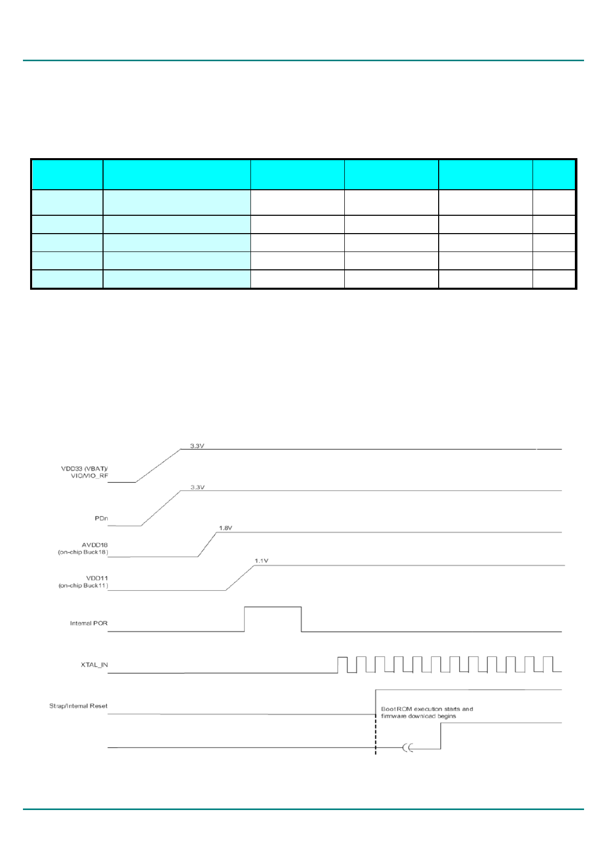
4.11Power up Timing Sequence
WIFI-2-V897EA1
IEEE 802.11a/b/g/n/ac 2T2R
Sichuan AI-Link Technology Co., Ltd. page 17 of 23
5. Interfaces
5.1.1 Host Interface
WIFI-2-V897EA1
IEEE 802.11a/b/g/n/ac 2T2R
Sichuan AI-Link Technology Co., Ltd. page 18 of 23
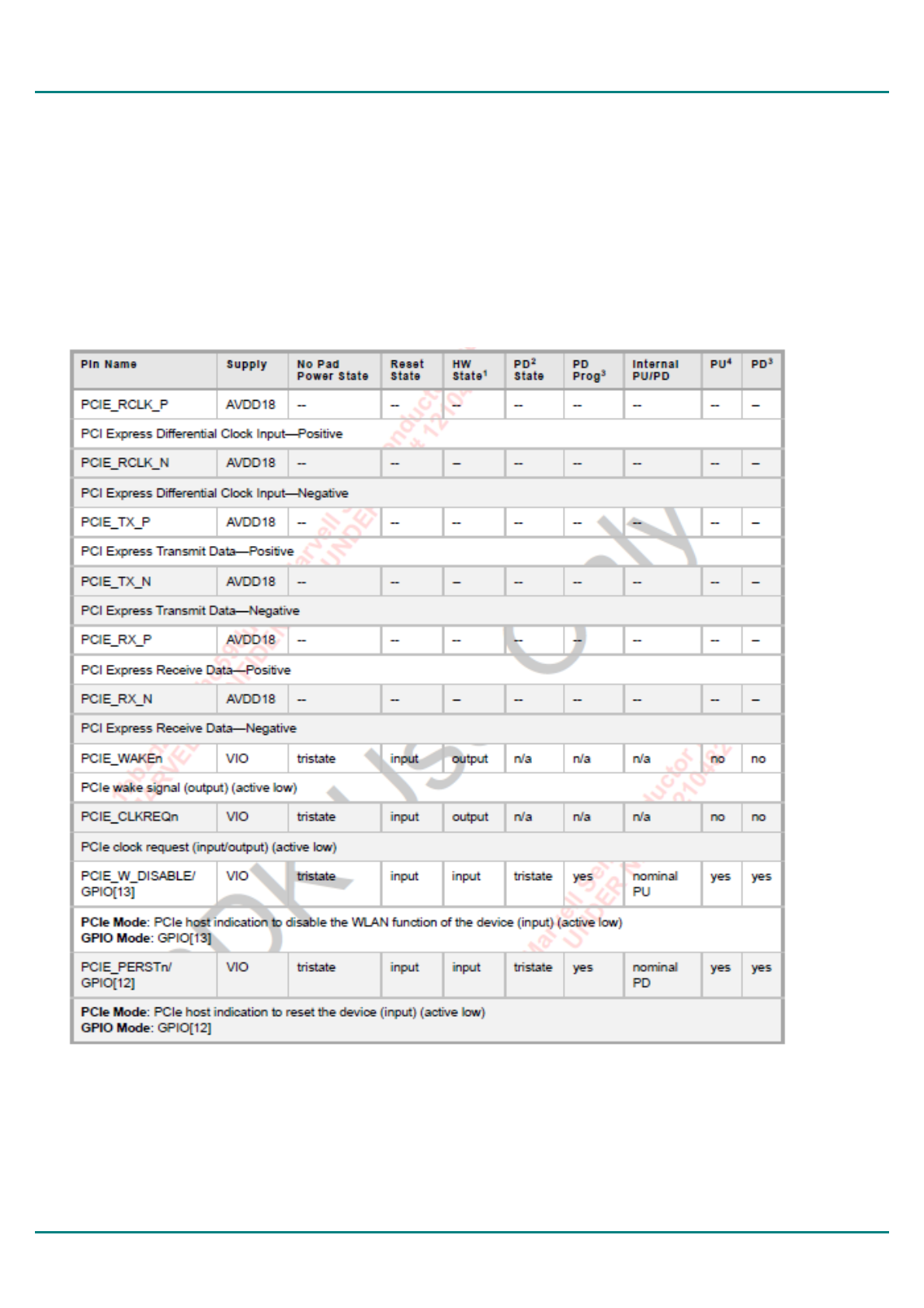
5.1.2 PCI Express Interface
WIFI-2-V897EA1
IEEE 802.11a/b/g/n/ac 2T2R
Sichuan AI-Link Technology Co., Ltd. page 19 of 23
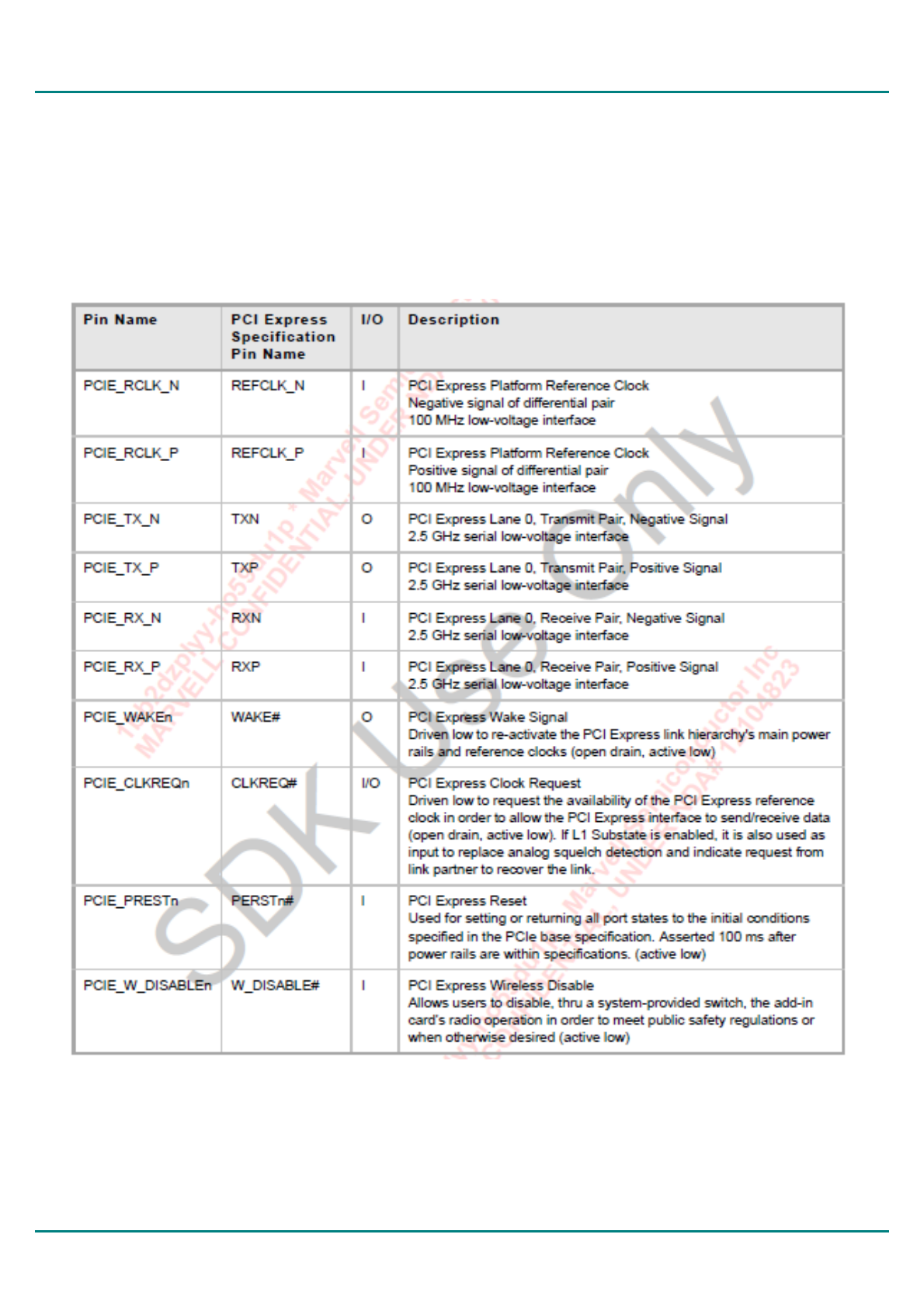
5.2 PCI Express Interface
5.2.1 Interface Signal Description
Symbol
Parameter
Min.
Typ.
Max.
Unit
UI
Unit interval
Each UI 400 ps±300 PPM
UI does not account for SSC dictated variations
399.98
400-
400.12
ps
VTX-DIFFpp
Differential peak-to-peak output voltage
VTX_DIFFpp=2*|VTX_D+ - VTX_D-|
0.8
-
1.2
V
VTX-DE-RATIO
De-emphasized differential output voltage(radio)
-3.0
-3.5
-4.0
dB
TRX-EYE
Minimum Tx eye width
0.75
-
-
UI
TRX-EYE-MEDIAN-_
MAX-JIT
Maximum time between jitter median and
maximum deviation from median
-
-
0.125
UI
TTX-RISE
TTX-FALL
D+/D- Tx output rise/fall time
0.125
-
-
UI
TTX-CM-DC-ACTIVE-
IDLE-DELTA
Absolute delta of DC common mode voltage
during L0 and electrical idle
0
-
100
mV
TTX-CM-DC-LINE-DE
LTA
Absolute delta of DC common mode voltage
between D+ and D-
0
-
25
mV
TTX-IDLE-DIFFp
Electrical idle differential peak output voltage
0
-
20
mV
TTX-RCV-DETECT
Voltage change allowed during receiver
detection
-
-
600
mV
TTX-DC-CM
Tx DC common mode voltage
-
-
3.6
V
TTX-SHORT
Tx short circuit current limit
-
-
90
mA
TTX-IDLE-MIN
Minimum time spent in electrical idle
50
-
-
UI
TTX-IDLE-SET-TO-ID
LE
Maximum time to transition to a valid electrical
idle after sending an electrical idle ordered set
-
-
20
UI
TTX-IDLE-TO-DIFF-D
TA
Maximum time to transition to valid Tx
specifications after leaving an electrical condition
-
-
20
UI
RLTX-DIFF
Differential return loss
10
-
-
dB
RLTX-CM
Common mode return loss
6
-
-
dB
CTX
AC coupling capacitor
7.5
-
200
nF
TCrosstalk
Crosstalk random timeout
0
-
1
ms
WIFI-2-V897EA1
IEEE 802.11a/b/g/n/ac 2T2R
Sichuan AI-Link Technology Co., Ltd. page 20 of 23
5.2.2 Differential Rx Output Electricals
Symbol
Parameter
Min.
Typ.
Max.
Unit
UI
Unit interval
Each UI 400 ps±300 PPM
UI does not account for SSC dictated variations
399.98
400-
400.12
ps
VRX-DIFFpp
Differential peak-to-peak output voltage
VRX_DIFFpp=2*|VTX_D+ - VTX_D-|
0.175
-
1.2
V
TRX-EYE
Minimum Tx eye width
0.4
-
-
UI
TRX-EYE-MEDIAN-_
MAX-JIT
Maximum time between jitter median and
maximum deviation from median
-
-
0.3
UI
VRX-CM-ACp
AC peak common mode input voltage
-
-
150
mV
RLRX-DIFF
Differential return loss
10
-
-
dB
RLRX-CM
Common mode return loss
6
-
-
dB
ZRX-DIFF-DC
DC differential input impedance
80
100
120
Ω
ZRX-DC
DC input impedance
40
50
60
Ω
ZRX-HIGH-IMP-DC-P
OS
Powered down DC input impedance positive
50
-
-
k
ZRX-HIGH-IMP-DC-N
EG
Powered down DC input impedance negative
1
-
-
kΩ
VRX-IDLE-DET-DIFF
pp
Electrical idle detect threshold
65
-
175
UI
TRX-IDLE-DET-DIFF-
ENTERTIME
Unexpected electrical idle enter detect threshold
integration time
-
-
10
UI
LRX-SKEW
Total skew
-
-2
0
dB
5.3 USB Interface
5.3.1 USB 2.0 Device Interface Description
Pin Name
USB 2.0 Specification
Pin Name
Description
Pin72/3V3_USB
VBUS
USB Bus Power Supply
On-board regulator regulates voltage from VBUS level to
voltage levels used by USB PHY
GND
USB Bus Ground
Common ground on SoC device
Pin70/USB_DP
D+
USB Data Plus
One of the differential data pair
Pin69/USB_DM
D-
USB Data Minus
One of the differential data pair

WIFI-2-V897EA1
IEEE 802.11a/b/g/n/ac 2T2R
Sichuan AI-Link Technology Co., Ltd. page 21 of 23
ftware Requirements
The driver supports the following operating systems: Linux, Microsoft Windows XP, Vista and Win7.
Mfg. software tool version is :
MFG-W8897-MF-WIFI-BT-NFC-NO-CAL-BRG-FC-WIN-X86-2.1.0.76-15.2.7.p22

WIFI-2-V897USA1
IEEE 802.11a/b/g/n/ac 2T2R
Sichuan AI-Link Technology Co., Ltd. page 22 of 23
7. Statement:
FCC Radiation Exposure Statement
Changes or modifications not expressly approved by the party responsible for compliance could void the user's authority to operate the equipment.
This equipment has been tested and found to comply with the limits for a Class B digital device, pursuant to Part 15 of the FCC Rules. These limits are
designed to provide reasonable protection against harmful interference in a residential installation. This equipment generates uses and can radiate radio
frequency energy and, if not installed and used in accordance with the
instructions, may cause harmful interference to radio communications. However, there is no guarantee that interference will not occur in a particular installation.
If this equipment does cause harmful interference to radio or television reception, which can be determined by turning the equipment off and on, the user is
encouraged to try to correct the interference by one or more of the following measures:
-- Reorient or relocate the receiving antenna.
-- Increase the separation between the equipment and receiver.
-- Connect the equipment into an outlet on a circuit different from that to which the receiver is connected.
-- Consult the dealer or an experienced radio/TV technician for help
This device complies with part 15 of the FCC rules. Operation is subject to the following two conditions (1)this device may not cause harmful interference, and
(2) this device must accept any interference received, including interference that may cause undesired operation.
FCC Radiation Exposure Statement
The modular can be installed or integrated in mobile or fix devices only. This modular be installed in any portable device, for example, USB dongle like
transmitters is forbidden. This modular complies with FCC RF radiation exposure limits set forth for an uncontrolled environment. This transmitter must not be
collocated or operating in conjunction with antenna or transmitter. If the FCC identification number is not visible when the module is installed inside another
device, then the outside of the device into which the module is installed must also display label referring to the enclosed module. This exterior label can use
wording such as the following:” Contains Transmitter Module FCC ID: 2ACHK- V897EA1 Or Contains FCC ID: 2ACHK- V897EA1 when the module is installed
inside another device, the user manual of this device must contain below warning statements;1. This device complies with Part 15 of the FCC Rules. Operation

WIFI-2-V897USA1
IEEE 802.11a/b/g/n/ac 2T2R
Sichuan AI-Link Technology Co., Ltd. page 23 of 23
is subject to the following two conditions :(1) This device may not cause harmful interference.(2) This device must accept any interference received, including
interference that may undesired operation.2. Changes or modifications not expressly approved by the party responsible for compliance could void the user's
authority to operate the equipment. The devices must be installed and used in strict accordance with the manufacturer’s instructions as described in the user
documentation that comes with the product. This device is intended only for OEM integrators under the followingconditions:1) The antenna must be installed
such that 20 cm is maintained between the antenna and user.2) The transmitter module may not be co-located with any other transmitter or antenna. Module
Antenna Type:
For 2.4GHz : Antenna 0: 1.8dBi, Antenna 1: 2.4dBi
For 5GHz: Antenna 0: 6dBi, Antenna 1: 6dBi