Ingenico GPRS ELITE 790 GPRS POINT OF SALE TERMINAL User Manual USERS MANUAL 2
Ingenico ELITE 790 GPRS POINT OF SALE TERMINAL USERS MANUAL 2
Ingenico >
Contents
- 1. USERS MANUAL 1
- 2. USERS MANUAL 2
USERS MANUAL 2

GSM/GPRS
Embedded Data/Fax/Voice Wireless Modem
MTMMC-G-F1
MTMMC-G-F2
Developer’s Guide

Wireless ModemModule MTMMC-G-F1 and MTMMC-G-F2 Developer’s Guide 2
ModemModule Developer’s Guide
MTMMC-G-F1 and MTMMC-G-F2
PN S000295A, Version A
07/15/03
Copyright
This publication may not be reproduced, in whole or in part, without prior expressed written permission from
Multi-Tech Systems, Inc. All rights reserved.
Copyright © 2003, by Multi-Tech Systems, Inc.
Multi-Tech Systems, Inc. makes no representations or warranties with respect to the contents hereof and
specifically disclaims any implied warranties of merchantability or fitness for any particular purpose. Furthermore,
Multi-Tech Systems, Inc. reserves the right to revise this publication and to make changes from time to time in
the content hereof without obligation of Multi-Tech Systems, Inc. to notify any person or organization of such
revisions or changes.
Revisions
Revision Level Date Description
A07/15/03 First release.
Patents
This device is covered by patent number 5,673,268.
Trademarks
Trademarks of Multi-Tech Systems, Inc. are ModemModule and the Multi-Tech logo.
MNP and Microcom Network Protocol are registered trademarks of Microcom, Inc.
Microsoft, Windows, Windows 95, and Windows NT are either registered trademarks or trademarks of Microsoft
Corporation in the United States and/or other countries.
World Headquarters
Multi-Tech Systems, Inc.
2205 Woodale Drive
Mounds View, Minnesota 55112
Phone: 763-785-3500 or 800-328-9717
Fax: 763-785-9874
Technical Support
Country By Email By Phone
France: support@multitech.fr (33) 1-64 61 09 81
India: support@multitechindia.com 91 (124) 6340778
U.K.: support@multitech.co.uk (44) 118 959 7774
U.S. and Canada: oemsales@multitech.com (800) 972-2439
Rest of the World: oemsales@multitech.com (763) 717-5863
Internet Address: http://www.multitech.com

Wireless ModemModule MTMMC-G-F1 and MTMMC-G-F2 Developer’s Guide 3
Table of Contents
CHAPTER 1 – PRODUCT DESCRIPTION AND SPECIFICATIONS ................................................................5
INTRODUCTION ...........................................................................................................................................................5
Scope of the Developer Guide ................................................................................................................................5
GENERAL CHARACTERISTICS ......................................................................................................................................6
General...................................................................................................................................................................6
Electrical ................................................................................................................................................................6
Mechanical .............................................................................................................................................................6
FEATURE DETAILS ......................................................................................................................................................6
Telephony ...............................................................................................................................................................6
Short Message Service (GSM and GPRS mode).....................................................................................................6
GSM Circuit Data Features ...................................................................................................................................7
GPRS Packet Data Features ..................................................................................................................................7
GSM Supplementary Services.................................................................................................................................7
Other Features .......................................................................................................................................................7
Interfaces................................................................................................................................................................7
FEATURE DESCRIPTIONS .............................................................................................................................................8
APPLICATIONS ............................................................................................................................................................9
MECHANICAL DESIGN OVERVIEW ............................................................................................................................10
CHAPTER 2 – MECHANICAL SPECIFICATIONS............................................................................................11
MECHANICAL DIMENSIONS.......................................................................................................................................11
CLIMATIC AND MECHANICAL ENVIRONMENT TESTING COMPLIANCE ......................................................................12
CHAPTER 3 – ELECTRICAL CHARACTERISTICS.........................................................................................13
INTRODUCTION .........................................................................................................................................................13
50-PIN CONNECTOR INTERFACES..............................................................................................................................14
50-Pin Connector Description..............................................................................................................................14
Power Supply........................................................................................................................................................17
Serial Link ............................................................................................................................................................19
ON / ~OFF Interface ............................................................................................................................................20
BOOT ...................................................................................................................................................................22
Reset Signal (~RST)..............................................................................................................................................22
Flashing LED .......................................................................................................................................................23
General Purpose Input/Output .............................................................................................................................24
Analog to Digital Converter.................................................................................................................................24
Audio Interface.....................................................................................................................................................25
SIM interface ........................................................................................................................................................29
SPI Bus .................................................................................................................................................................31
Keypad Interface ..................................................................................................................................................31
CHAPTER 4 – INTERFACES .................................................................................................................................32
FLASHING LED.........................................................................................................................................................32
SIM INTERFACE........................................................................................................................................................32
RF INTERFACE ..........................................................................................................................................................33
RF Connector .......................................................................................................................................................33
RF Performances..................................................................................................................................................33
DTE/DCE INTERFACE RATES...................................................................................................................................33
CHAPTER 5 – TEST BOARD .................................................................................................................................34
SERIAL TEST/DEMO BOARD COMPONENTS...............................................................................................................34
SERIAL TEST/DEMO BOARD BLOCK DIAGRAM .........................................................................................................35
SIM Schematic (5V)..............................................................................................................................................36
CHAPTER 6 – APPLICATION CONSIDERATIONS..........................................................................................37

Wireless ModemModule MTMMC-G-F1 and MTMMC-G-F2 Developer’s Guide 4
GENERAL GUIDELINES FOR THE USE OF THE MODEMMODULE.................................................................................37
Hardware and RF.................................................................................................................................................37
The Antenna..........................................................................................................................................................37
Firmware Upgrade...............................................................................................................................................37
Initial Configuration Using Mobile PhoneTools..................................................................................................37
Getting Started .....................................................................................................................................................38
REFERENCE DOCUMENTS..........................................................................................................................................39
RELATED MANUALS .................................................................................................................................................39
ADDITIONAL INFORMATION......................................................................................................................................40
APPENDIX A – SAFETY PRECAUTIONS & REGULATORY STANDARDS COMPLIANCE....................41
SAFETY PRECAUTIONS..............................................................................................................................................41
RF Safety ..............................................................................................................................................................41
General Safety ......................................................................................................................................................42
Safety Standards...................................................................................................................................................42
RF Exposures .......................................................................................................................................................43
Instructions to OEMs............................................................................................................................................43
REGULATORY STANDARDS COMPLIANCE .................................................................................................................44
GSM compliance ..................................................................................................................................................44
FTA Compliance...................................................................................................................................................45
APPENDIX B – SOURCING GUIDE FOR CONNECTORS AND PERIPHERAL DEVICES........................46
WHERE TO FIND SMD CONNECTORS........................................................................................................................46
GSM ANTENNA........................................................................................................................................................47
SIM CARD HOLDER..................................................................................................................................................47
APPENDIX C – AT COMMAND LIST ..................................................................................................................48
APPENDIX D – ACRONYMS AND ABBREVIATIONS .....................................................................................53
INDEX ........................................................................................................................................................................54
LIST OF TABLES...................................................................................................................................................57
Chapter 1 – Product Description & Specification
Wireless ModemModule MTMMC-G-F1 and MTMMC-G-F2 Developer’s Guide 5
Chapter 1 – Product Description and Specifications
Introduction
ModemModule GSM/GPRS integrated wireless modems provide a quick and easy way to insert GSM and GPRS
functionality into systems and terminals. Available in dual-band configurations, this fully type approved integrated
modem constitutes a self-contained, fully integrated implementation of the GSM/GPRS standard. Thanks to
standard interfaces, it can be integrated into any system. It is ready for voice, SMS, data and fax. ModemModule
GSM/GPRS is a product with a single connector, which puts together all interface signals in order to facilitate its
integration. It has an integrated SIM connector as well as a standard RF connector type MMCX. For system
integrators, ModemModule GSM/GPRS is the fast track to the wireless world.
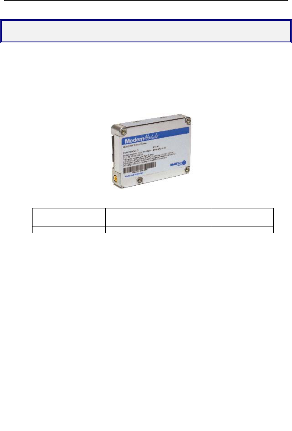
Figure 1-1: MultiTech’s Wireless ModemModule GSM/GPRS
Product Description Region
MTMMC-G-F1 GSM/GPRS Class 10, 900/1800 MHz Global
MTMMC-G-F2 GSM/GPRS Class 10, 850/1900 MHz Global
The MTMMC-G-F1 and MTMMC-G-F2 ModemModules are used to integrate wIreless data and fax
communications in numerous embedded applications.
Scope of the Developer Guide
This document describes the hardware interface and the technical specifications of the ModemModule
GSM/GPRS wireless modems. The integrated modem is referred to as ModemModule GSM/GPRS according to
the GSM/GPRS 900 standard, the GSM/GPRS 1800 standard and the GSM/GPRS 1900 standard. This product
is based on a Dual Band RF module: every integrated modem referenced ModemModule GSM/GPRS-
G900/1800 includes a GSM 900/1800 MHz module and every integrated modem referenced ModemModule
GSM/GPRS-G850/1900 includes a GSM 850/1900 MHz module. These two dual-band modems have the same
specifications unless otherwise specified.

Chapter 1 – Product Description & Specification
Wireless ModemModule MTMMC-G-F1 and MTMMC-G-F2 Developer’s Guide 6
General Characteristics
General
· GPRS Class 10
· Dual Band GSM/GPRS modem E-GSM 900/1800 or GSM 850/1900
· 2W at 850MHz
· 1W at 1800/1900 MHz
· GSM Class 1 and Class 2 Group 3 FAX
· Small size and low power consumption
· Voice and Short Message Services (SMS)
· Fax and data transmission without extra hardware
· Serial interface supports DTE speeds up to 115.2K
· MMCX connector and SIM socket
· 14.4K GSM circuit-switched data
· Tricodec (FR/EFR/HR)
· Internal 3V SIM interface
· Easy remote control by AT commands for dedicated applications
· Fully Type Approved according to GSM Phase 2+ specifications
· Board-to-board or board-to-cable mounting
· Fully shielded and ready-to-use
Electrical
· Power supply: 5 VDC +/- 5% 1A
Mechanical
· Absolute maximum dimension: 46 x 64 x 12 mm
· Weight: 79 g
· Casing: Complete shielding-stainless steel/zinc
· Mounting: 4 screw holes
· Operating temperature range: -30°C to + 60°C
· Storage temperature: -35°C to +85°C
Feature Details
Telephony
· Telephony (TCH/FS) & Emergency calls
· Full Rate, Enhanced Full Rate and Half Rate
· Dual Tone Multi Frequency function (DTMF)
Short Message Service (GSM and GPRS mode)
· Text and PDU
· Point to point MT & MO
· SMS Cell Broadcast

Chapter 1 – Product Description & Specification
Wireless ModemModule MTMMC-G-F1 and MTMMC-G-F2 Developer’s Guide 7
GSM Circuit Data Features
· Data circuit asynchronous, transparent and non transparent up to 14,400
· bits/s
· Automatic fax group 3 (Class 1 & 2)
· Alternate speech and fax
· MNP2, V.42bis data compression
GPRS Packet Data Features
· GPRS Class 10
· Coding Schemes: C1S1 to CS4
GSM Supplementary Services
· Call Forwarding
· Call Barring
· Multiparty
· Call Waiting and Call Hold
· Calling Line Identity
· Advice of Charge
· USSD
· Closed User Group
· Explicit Call Transfer
Other Features
· ME+SIM phone book management
· Fixed Dialing Number
· SIM Toolkit Class 2
· SIM, network and service provider locks
· Real Time Clock
· Alarm management
· Software upgrade through Xmodem protocol
· UCS2 character set management
Interfaces
Single antenna interface
Internal SIM interface: 3V only
External SIM interface: 3V or 5V
For Data Operation:
Serial link
Remote control by AT commands (GSM 07.07 and 07.05)
Baud rate from 300 to 115,200 bits/s
From 300 up to 38400 bits/s with autobauding
The integrated modem has a sole 50-pin connector, which gathers all the interface signals in order to facilitate its
integration. It has an integrated SIM card holder as well as a standard RF connector type MMCX. The concept
of the integrated modem has been defined to integrate on a sole device:
· a single connector has been used that is standard and easy to find (it is supplied worldwide);
this connector includes all of the modem’s analog and digital connections
· One standard easy to find RF connector. See RF connector section in Chapter 3: Electrical
Characteristics;
· One SIM card holder. See SIM section in Chapter 3: Electrical Characteristics.

Chapter 1 – Product Description & Specification
Wireless ModemModule MTMMC-G-F1 and MTMMC-G-F2 Developer’s Guide 8
Feature Descriptions
Integration Reduces Space, Power and Cost. The ModemModule GSM/GPRS integrates the
controller, RF transceiver, and antenna interface in one compact unit. This integration requires low power,
occupies very little space, and provides an overall reduction in costs.
Reduces Development Time. The ModemModule GSM/GPRS can make your existing and next
generation device, machine, or system, communication-ready without requiring significant hardware
changes to its design. It actually provides faster time-to-market because it relieves the burden and expense
of obtaining network and RF approvals. This complete, ready-to-integrate wireless module allows you to
enhance your product while you focus on developing its core features.
Voice Features. The ModemModule GSM/GPRS provides telephony and Dual Tone Multi Frequency (DTMF)
functionality. It also allows for emergency calls as well as full rate, enhanced Full Rate and Half Rate
(FR/EFR/HR).
Short Message Services. The ModemModule GSM/ GPRS offers SMS features such as text and PDU, point-
to-point (MT/MO) and cell broadcast.
Compatible Supplementary Services. The ModemModule GSM/GPRS is compatible with supplementary
services such as call forwarding, call barring, multiparty, call waiting and call hold, calling line identification,
advice of charge, USSD, closed user group and explicit call transfer.
Management Features. The ModemModule GSM/ GPRS provides advanced management features including
phone book management, fixed dialing number, real time clock and alarm management.
Industry-standard Modem Commands. The ModemModule GSM/GPRS provides industry-standard
AT-style commands for ease of integration into your existing software application.
ModemModule Pin-Out. The ModemModule GSM/ GPRS interfaces easily with existing products
through a standard serial communication channel. The complete on-board RF transceiver interfaces with
an antenna for direct connection to wireless SMS, circuit-switched dial-up, or packet data networks. The
ModemModule is a Data Terminal Equipment (DTE) device with serial asynchronous protocol support. The
serial DTE channel is capable of transfer speeds to 115.2K bps and can be interfaced directly to a UART
or microcontroller. It can be board-to-board or board-to-cable mounted.
Network and RF Approved. The ModemModule GSM/ GPRS has been tested and certified with
wireless telecom network providers worldwide. In addition, it has successfully completed worldwide
compliance
Developer’s Kit. The ModemModule GSM/GPRS Developer’s Kit allows you to plug in the
ModemModule and use it for testing, programming and resolving application issues.

Chapter 1 – Product Description & Specification
Wireless ModemModule MTMMC-G-F1 and MTMMC-G-F2 Developer’s Guide 9
Applications
With circuit switched data rates up to 14.4K bps, the MultiModem GSM/GPRS is targeted at applications that
periodically need to send or receive data over a wireless network. It is an ideal device for:
Appliances Remote Diagnostics
ATM Terminals Remote Metering
Automotive Security Systems
Data Collection Vending/Gaming
Machines
Gas Pumps Other devices requiring
wireless connectivity.
Industrial and Medical
Remote Monitoring
Systems
Note: The Wireless
MultiModem must be
mounted with at least 8
inches (20 cm) of clearance
from the human body.
Chapter 1 – Product Description & Specification
Wireless ModemModule MTMMC-G-F1 and MTMMC-G-F2 Developer’s Guide 10
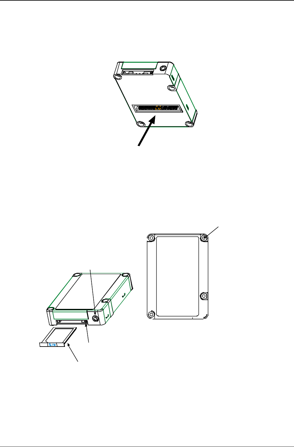
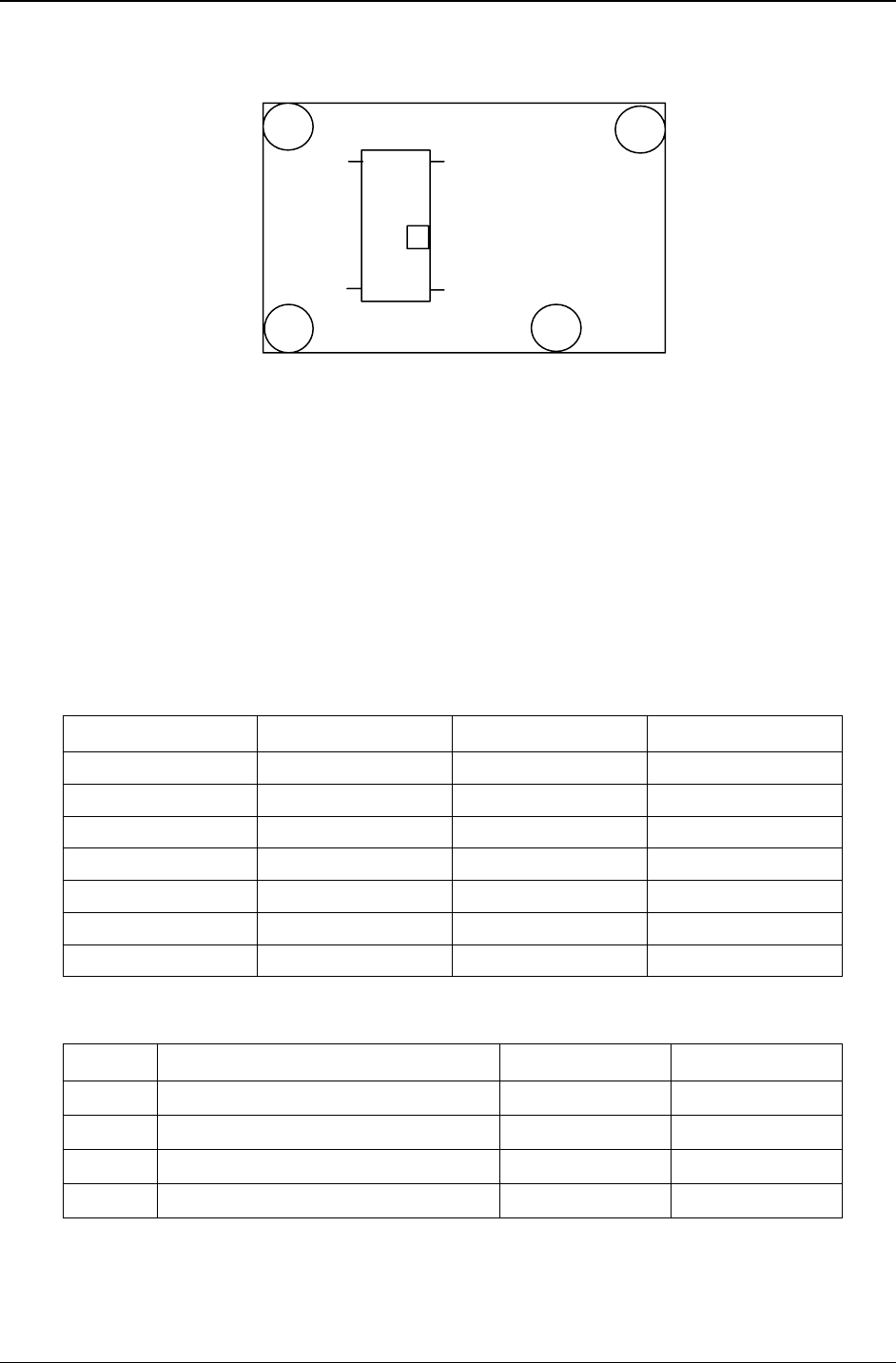
Mechanical Design Overview
The ModemModule is encased as shown in the figure below. It includes a RF module, a 50-pin connector, a SIM
holder and a RF connector.
Interface Connector
Figure 1-2: Mechanical Description A
Holes for Mounting
Screws (4)
Hole dia. = 0.087”
SIM Reader
Antenna Connector
(MMCX type)
SIM ejection button
Figure 1-3: Mechanical Description B
Four screw holes allow the ModemModule to be fixed on the mother PCB. The ModemModule can be mounted
indifferently on both sides (top or bottom). For further details see Chapter 2: Mechanical Specifications.
Chapter 2 – Mechanical Specifications
Wireless ModemModule MTMMC-G-F1 and MTMMC-G-F2 Developer’s Guide 11
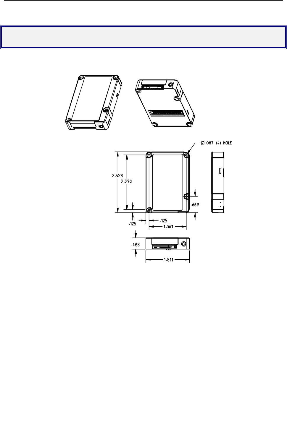
Chapter 2 – Mechanical Specifications
Mechanical Dimensions
Figure 2-1: ModemModule Dimensions

Chapter 2 – Mechanical Specifications
Wireless ModemModule MTMMC-G-F1 and MTMMC-G-F2 Developer’s Guide 12
Climatic and Mechanical Environment Testing Compliance
Table 2-1 : Climatic and Mechanical Environment Testing Compliance
G900/G1800 Environmental
Type of Test Standards Storage
Class 1.2
Transportation
Class 2.3
Operating (Port Use)
Class 7.3
Cold IEC 68-2.1
Ab test
-25O C; 72 hours -40O C; 72 hours -20O C (GSM); 16 hours
-10O C (DCS) 16 hours
Dry Heat IEC 68-2.2
Bb test
+70O C; 72 hours +70O C; 72 hours +55O C; 16 hours
Change of
Temperature
IEC 68-2.14;
Na/Nb test -40O/+30O C; 5 cycles
t1 = 3 hours
-20O/+30O C (GSM); 3 cycles
-10O/+30O C (DCS); 3 cycles
t1 = 3 hours
Damp Heat
Cyclic
IEC 68-2.30;
Db test +30O C; 2 cycles
90% - 100% RH
variant 1
+40O C; 2 cycles
90% - 100% RH
variant 1
+40O C; 2 cycles
90% - 100% RH
variant 1
Damp Heat IEC 68-2.56
Cb test
+30O C; 4 days +40O C; 4 days +40O C; 4 days
Sinusoidal
Vibration
IEC 68-2.6
Fc test
5 - 62 Hz : 5 mm/s
62 – 200 Hz: 2 m/s2
3 x 5 sweep cycles
Random
Vibration
IEC 68-3.36
Fdb test
5 – 20 Hz: 0.96 m2/s3
20 – 500 Hz: -3 dB/ oct
3 x 10 min
10 – 12 Hz: 0.96 m2/s3
12 – 150 Hz: -3 dB/ oct
3 x 30 min

Chapter 3 – Electrical Characteristics
Wireless ModemModule MTMMC-G-F1 and MTMMC-G-F2 Developer’s Guide 13
Chapter 3 – Electrical Characteristics
Introduction
This chapter describes the ModemModule’s electrical interfaces. These are:
· interfaces on the 50-pin general purpose connector (power and data/signaling)
· RF interface
· SIM interface

Chapter 3 – Electrical Characteristics
Wireless ModemModule MTMMC-G-F1 and MTMMC-G-F2 Developer’s Guide 14
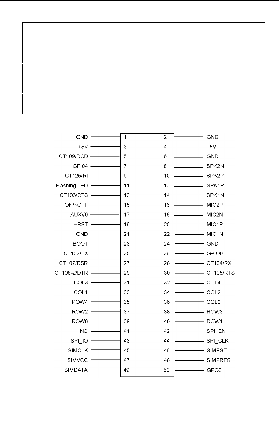
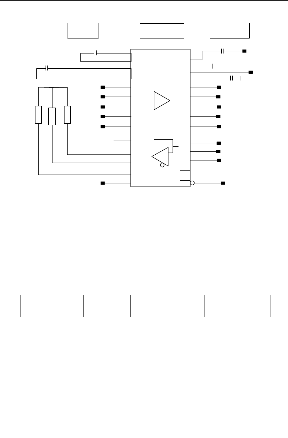
50-Pin Connector Interfaces
50-Pin Connector Description
Table 3-1. 50-pin Connector Description
Pin # Name I/O I/O Type Description Comment
1 GND GROUND High current
2 GND GROUND High current
3 +5V Supply High current
4 +5V Supply High current
5 CT109/DCD O CMOS/2X Data Carrier Detect
6 GND GROUND High current
7 GPI04 I/O CMOS/2X General Purpose I/O
8 SPK2N O Analog Speaker 2 negative output
9 CT125/RI O CMOS/2X Ring Indicator
10 SPK2P O Analog Speaker 2 positive output
11 Flashing LED I/O CMOS/2X Working mode indication
LED
Driven by
module
12 SPK1P O Analog Speaker 1 positive output
13 CT106/CTS O 1X Clear to Send
14 SPK1N O Analog Speaker 1 negative output
15 ON/~OFF I Power ON/OFF control ON = Vcc
16 MIC2P I Analog Microphone 2 positive
input
17 AUXV0 I Analog Auxiliary ADC input
18 MIC2N I Analog Microphone 2 negative
input
19 ~RST I Reset active low Open Collector
20 MIC1P I Analog Microphone 1 positive
input
21 GND I Ground
22 MIC1N I Analog Microphone 1 negative
input
23 BOOT I BOOT Open Collector
24 GND GROUND High Current
25 CT103/TX I Transmit Data Pull up with
100K-ohm
when not used

Chapter 3 – Electrical Characteristics
Wireless ModemModule MTMMC-G-F1 and MTMMC-G-F2 Developer’s Guide 15
Table 3-1. 50-Pin Connector Description (Continued)
Pin # Name I/O I/O Type Description Comment
26 GPIO0 I/O CMOS/2X General Purpose I/O
27 CT107/DSR O 1X Data Set Ready
28 CT104/RX O 1X Receive Data
29 CT108-2/DTR I Data Terminal Ready Pull up with
100K-ohm
when not used
30 CT105/RTS I Request to Send Pull up with
100K-ohm
when not used
31 COL3 I/O 1X Keypad column
32 COL4 I/O 1X Keypad column
33 COL1 I/O 1X Keypad column
34 COL2 I/O 1X Keypad column
35 ROW4 I/O 1X Keypad row
36 COL0 I/O 1X Keypad column
37 ROW2 I/O 1X Keypad row
38 ROW3 I/O 1X Keypad row
39 ROW0 I/O 1X Keypad row
40 ROW1 I/O 1X Keypad row
41 NC Not Connected
42 SPI_EN O 1X SPI enable
43 SPI_IO I/O 1X I2C Data or SPI Data
44 SPI_CLK O 2X I2C Clock or SPI Clock
45 SIMCLK O 2X Clock for SIM interface 3V mode
46 SIMRST O 2X Reset for SIM interface 3V mode
47 SIMVCC O SIM card supply 3V mode
6mA max.
48 SIMPRES I SIM card detect Connected to
SIM connector
pin 8. Pin 4 of
SIM connector
must be pulled
down to GND
with 1 K-Ohm*
49 SIMDATA I/O 3X I/O for SIM interface 3V mode
50 GPO0 General purpose I/O
* See SIM socket diagram in SIM interface section
** GPO0 is a general purpose output for selection of external SIM, 3V or 5V.
Chapter 3 – Electrical Characteristics
Wireless ModemModule MTMMC-G-F1 and MTMMC-G-F2 Developer’s Guide 16
Table 3-2. Operating Conditions
Parameter I/O Type Min Max Condition
Vinput low CMOS -0.5V 0.8V
Vinput high CMOS 2.1V 3.0V
1X 0.2V IOL = -1mA
2X 0.2V IOL = -2mA
Voutput low
3X 0.2V IOL = -3mA
1X 2.6V IOH = 1mA
2X 2.6V IOH = 2mA
Voutput high
3X 2.6V IOH = 3mA
Figure 3-1: 50-Pin Connector
Chapter 3 – Electrical Characteristics
Wireless ModemModule MTMMC-G-F1 and MTMMC-G-F2 Developer’s Guide 17
50 49
21
Figure 3-2: Pin Numbering – Bottom View
Power Supply
The main power supply is provided through a double connection. These connections are respectively pins 3 and
4 for the +5V and the pins 1 and 2 for the ground (GND). The pins 6, 21, and 24 are also ground connection in
order to produce a proper ground plane.
A 5V +/-5% - 1A power is strictly required to supply the modem. Otherwise, serious dysfunctions may appear.
However, the modem does not have to constantly deliver 1A current at 5V on this power supply.
This power supply is internally regulated to a nominal value VBATT.
Table 3-3: Power Supply Pin Description
Pin Number Name Description Comment
1 GND Ground High Current
2 GND Ground High Current
3 +5V Ground High Current
4 +5V Ground High Current
6 GND Ground High Current
21 GND Ground High Current
24 GND Ground High Current
Table 3-4: Power Consumption in EGSM-only mode @25 degrees C
Conditions INOM IMAX
+5V During TX bursts @2W 810 mA 1 A
+5V Average @ 2W 310 mA 370 mA
+5V Average @ ).5W 185 mA 200 mA
+5V Average idle mode 22 mA 25 mA

Chapter 3 – Electrical Characteristics
Wireless ModemModule MTMMC-G-F1 and MTMMC-G-F2 Developer’s Guide 18
Table 3-5: Power Consumption in GSM-only 1800 & 1900 MHz modes @25 degrees C
Conditions INOM IMAX
+5V During TX bursts @1W 635 mA 800 mA
+5V Average @1W 260 mA 280 mA
+5V Average @ 0.25W 150 mA 170 mA
+5V Average idle mode 20 mA 22 mA
Table 3-6: Power Consumption in EGSM/GPRS 900 MHz and GSM/GRPS 850 MHz Mode
Class 10
Conditions INOM IMAX
+5V During TX bursts @PcI5 1.7 A peak 2.0 A peak
+5V During RX bursts 75 mA peak 80 mA peak
+5V Average 1Rx/1Tx @PcI5 270 mA 320 mA
+5V Average 1Rx/1Tx@PcI8 180 mA 200 mA
+5V Average idle mode 100 mA 300 mA
+5V Average GPRS CI 10
(3Rx/2Tx) @PcI5
540 mA 640 mA
+5V Average GPRS CI 10
(3Rx/2Tx) @PcI8
360 mA 400 ma
+5V Average Idle mode 2,2 mA 3 Ma
Power Control Level: PcI5=2W typ.; PcI8=0,5W typ.
Table 3-7: Power Consumption in GSM/GRPS 1800 MHz and GSM/GRPS 1900 MHz
Class 10
Conditions INOM IMAX
+5V During TX bursts @PcI0 1.3 A peak 1.7 A peak
+5V During RX bursts 75 mA peak 80 mA peak
+5V Average 1Rx/1Tx @PcI5 240 mA 270 mA
+5V Average 1Rx/1Tx@PcI8 150 mA 180 mA
+5V Average idle mode 100 mA 300 mA
+5V Average GPRS CI 10
(3Rx/2Tx) @PcI5
480 mA 540 mA
+5V Average GPRS CI 10
(3Rx/2Tx) @PcI8
300 mA 360 Ma
+5V Average Idle mode 2,2 mA 3 Ma
Power Control Level: PcI0=1W typ; PcI3=0,25W typ

Chapter 3 – Electrical Characteristics
Wireless ModemModule MTMMC-G-F1 and MTMMC-G-F2 Developer’s Guide 19
Serial Link
A serial link interface is available complying with V24 protocol signaling but not with V28 (electrical interface) due
to a 2.8 Volts interface. TX, RTS and DTR can be either 5V or 3V.
The signals are Tx data (CT103/TX), Rx data (CT104/RX), Request To Send (CT105/RTS), Clear To Send
(CT106/CTS), Data Terminal Ready (CT108-2/DTR) and Data Set Ready (CT107/DSR).
The set of RS232 signals can be required for GSM DATA services application. The 2 additional signals are Data
Carrier Detect (CT109/DCD) and Ring Indicator (CT125/RI).
Table 3-8: Serial Link Pin Description
Signal Pin Number I/O I/O Type* Description
CT103 / TX 25 I CMOS Transmit serial data
CT104 / RX 28 O 1X Receive serial data
CT105 / RTS 30 I CMOS Ready to send
CT106 / CTS 13 O 1X Clear to send
CT107 / DSR 27 O 1X Data set ready
CT108-2 / DTR 29 I CMOS Data terminal ready
CT109 / DCD 5 O CMOS / 2X Data carrier detect
CT125 / RI 9 O CMOS / 2X Ring indicator
* See “Table 3-2: Operating Conditions” in section on the 50-pin Connector Description.
Chapter 3 – Electrical Characteristics
Wireless ModemModule MTMMC-G-F1 and MTMMC-G-F2 Developer’s Guide 20
Modem Te rm in a lLevel Shifter
Vcc
RI
DCD
RX
CTS
DSR
DTR
TX
RTS
Vcc
28
25
1
3
24
23
22
19
17
16
21
20
18
13
C1+
C1-
C2+
T1IN
T2IN
T3IN
T4IN
T5IN
R1OUTB
R2OUT
R3OUT
R4OUT
ON
C2-
T1OUT
T2OUT
T3OUT
T4OUT
T5OUT
R1IN
R2IN
R3IN
ERROR
OFF
27
2
26
4
5
6
7
10
12
8
9
11
15
14
S_RI
S_DCD
S_RX
S_CTS
S_DSR
S_DTR
S_TX
S_RTS
Vcc
Vcc
GND
Vcc
GND
MAX 3238
*Th is appli cation n ote i s valid for Vcc> 3.0 Volt (see MAX 3 238 sp ecification s)
Auto shut d own mode is no t used in th is exa mp le.
Figure 3-3: Level Shifter Application Diagram for Serial Link
ON / ~OFF Interface
This input is used to switch ON or OFF the ModemModule. A high level signal has to be provided on the
ON/~OFF pin to switch on the modem. The level of the voltage of this signal has to be maintained to VCC during
a minimum time of 1 second. When powered off, the shutdown current is roughly 60 microAmperes.
Table 3-9: ON / OFF Pin Description
Signal Pin Number I/O I/O Type* Description
ON / ~OFF 15 I CMOS Module Power ON/OFF
Chapter 3 – Electrical Characteristics
Wireless ModemModule MTMMC-G-F1 and MTMMC-G-F2 Developer’s Guide 21
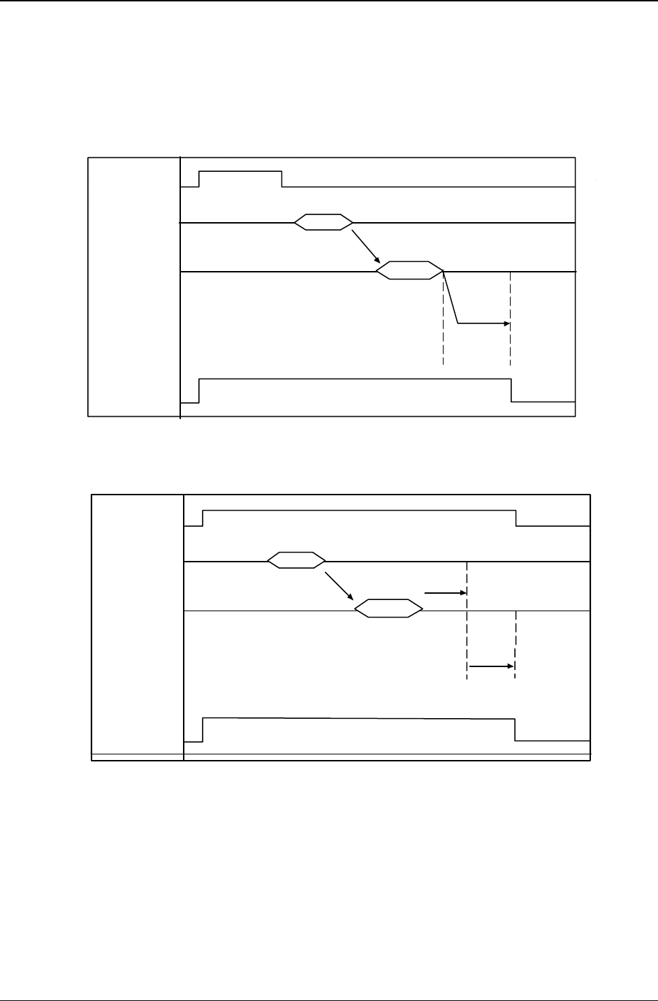
Power OFF Procedure
In order to power OFF the ModemModule, switch it OFF both via software (AT+CPOF; see AT Command
Manual for more details) and via hardware line. See the diagrams below.
ON/~OFF
AT +C P O F
Serial Link
to ModemModule
OK res p o nse
Serial Link
from
Modem Module
About
500 ms
Mo de m Mod ul e
Stat u s ___
ON
OFF___
Figure 3-4: Power-Off Procedure 1
ON /~ O FF
AT+ CP O F
Seria l Li nk
to ModemModule
OK response
Seria l Li nk
from
ModemModule
___
ON
OF F__ _
About
500 ms
ModemModule
Stat us
About
500 ms
Figure 3-5: Power-Off Procedure 2
Chapter 3 – Electrical Characteristics
Wireless ModemModule MTMMC-G-F1 and MTMMC-G-F2 Developer’s Guide 22
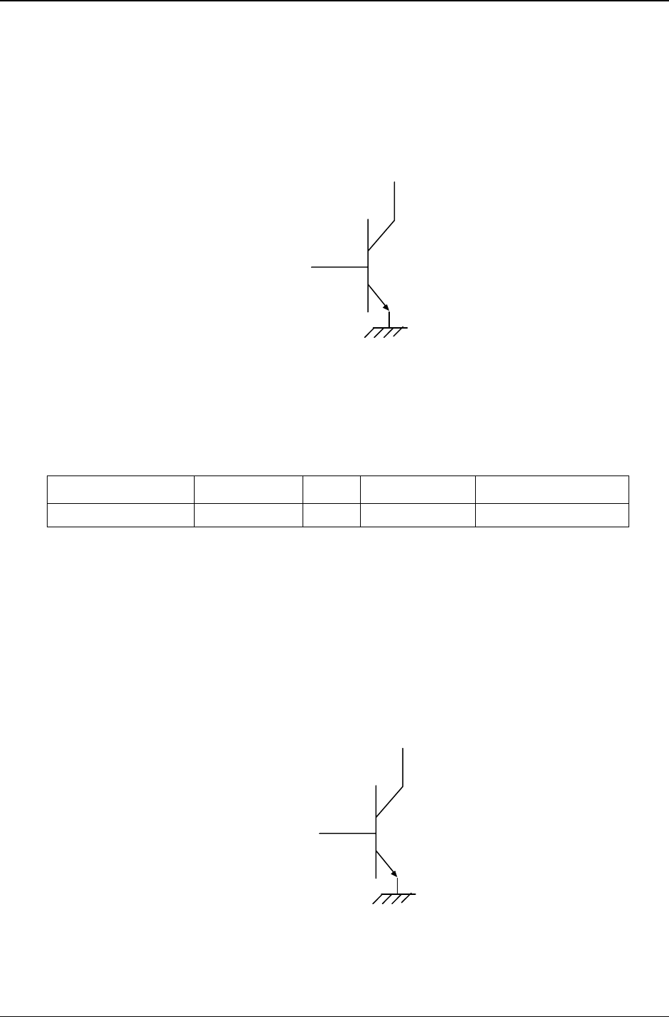
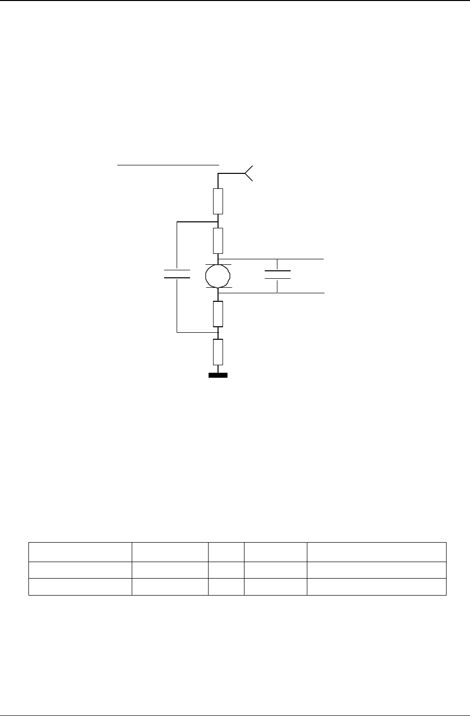
BOOT
This input is used to switch the ModemModule into download mode (backup procedure). The internal boot
procedure is started when this pin is low during the power ON of the module. In normal mode, this pin has to be
left open. If used, this input has to be driven by an open collector or an open drain. See below an example of
application diagram. See also the “Firmware Upgrade” section of Chapter 5: Application Considerations.
BOOT : Pin 23
Switch BOOT
Figure 3-6: Boot Procedure
If Switch Boot = 1, Boot pin 23 = 0, to download mode
If Switch Boot = 0, Boot pin 23 = 1, to normal mode
Table 3-10: BOOT Pin Description
Signal Pin Number I/O I/O Type* Description
BOOT 23 I CMOS SW downloading
* See “Table 3-2: Operating Conditions” in section on the 50-pin Connector Description.
Reset Signal (~RST)
This signal is used to force a reset of the ModemModule. It has to be used by providing low level during
approximately 2ms. This signal has to be considered as an emergency reset only. A reset procedure is already
driven by an internal hardware during the power-up sequence.
This signal can also be used to provide a reset to an external device. If no external reset is necessary this input
can be left open. If used (emergency reset), it has to be driven by an open collector or an open drain. See below
an example of application diagram.
Reset : Pin 23
Switch Reset
Figure 3-7: Reset Procedure
If switch Reset = 1, Reset pin 19 = 0
If switch Reset = 0, Reset pin 19 = 1

Chapter 3 – Electrical Characteristics
Wireless ModemModule MTMMC-G-F1 and MTMMC-G-F2 Developer’s Guide 23
Table 3-11: Reset Signal Pin Description
Signal Pin Number I/O I/O Type* Description
~RST 19 I/O Module reset
* See “Table 3-2: Operating Conditions” in section on the 50-pin Connector Description.
Table 3-12: Reset Signal Electrical Characteristics
Parameter Min Max Unit
Input Impedance ( R ) 4.7 kilo-ohms
Input Impedance ( C ) 10 nanofarads
Table 3-13: Reset Signal Operating Conditions
Parameter Min Max Condition
*VT- 1.1 V 1.2 V
*VT+ 1.7 V 1.9 V
VOL 0.4 V IOL = -50 microamperes
VOH 2.0 V IOH = -50 microamperes
VT-, VT+ hysteresis level
Flashing LED
The flashing LED signal is used to indicate the working mode of the ModemModule.
Table 3-14 : Flashing LED Pin Description
Signal Pin Number I/O I/O Type* Description
Flashing LED 11 I/O CMOS/2X Working mode
indication LED
* See “Table 3-2: Operating Conditions” in section on the 50-pin Connector Description.
Table 3-15 : LED and ModemModule Status
LED Indication ModemModule Status
OFF Download mode or switched OFF.
Permanent Switched ON, not registered on the network.ON
Flash Switched ON, registered on the network.

Chapter 3 – Electrical Characteristics
Wireless ModemModule MTMMC-G-F1 and MTMMC-G-F2 Developer’s Guide 24
General Purpose Input/Output
The ModemModule provides two General Purpose I/O connections. They can be used to control any external
device.
Table 3-16 : General Purpose I/O Pin Description
Signal Pin Number I/O I/O Type* Description Default Value
GPIO0 26 I/O CMOS / 2X General Purpose I/O 0
GPIO4 7 I/O CMOS / 2X General Purpose I/O 0
* See “Table 3-2: Operating Conditions” in section on the 50-pin Connector Description.
All digital I/O complies with 3Volts CMOS.
You can access (write or read) the GPIO value via AT+WIOW and AT+WIOR. See AT Command manual for
more details.
Analog to Digital Converter
The ModemModule has an Analog to Digital converter (ADC) input. This converter is a 10 bits one, ranging from
0 to 2.5V. You can see the measurements via AT+ADC. See AT Command manual for more details.
Table 3-17: A/D Converter Pin Description
Signal Pin Number I/O I/O Type* Description
AUXV0 17 I Analog A/D converter
* See “Table 3-2: Operating Conditions” in section on the 50-pin Connector Description.
Table 3-18: A/D Converter Electrical Characteristics
Parameter Min Max Unit
Resolution 10 bits
Sampling Rate 90.3 Ksps
Input Signal Range 0 2.5V Volts
ADC Reference Accuracy 0.5 %
Integral Accuracy +/- 1 LSB
Differential Accuracy +/- 1 LSB
Input Impedance ( R ) 10 mega-
Ohms
Input Impedance ( C ) 50 pico-
Farads
Chapter 3 – Electrical Characteristics
Wireless ModemModule MTMMC-G-F1 and MTMMC-G-F2 Developer’s Guide 25
Audio Interface
Two different microphone inputs and two different speaker outputs are supported. The connection can be either
differential or single-ended but using a differential connection in order to reject common mode noise and TDMA
noise is recommended.
Microphone 2 Inputs
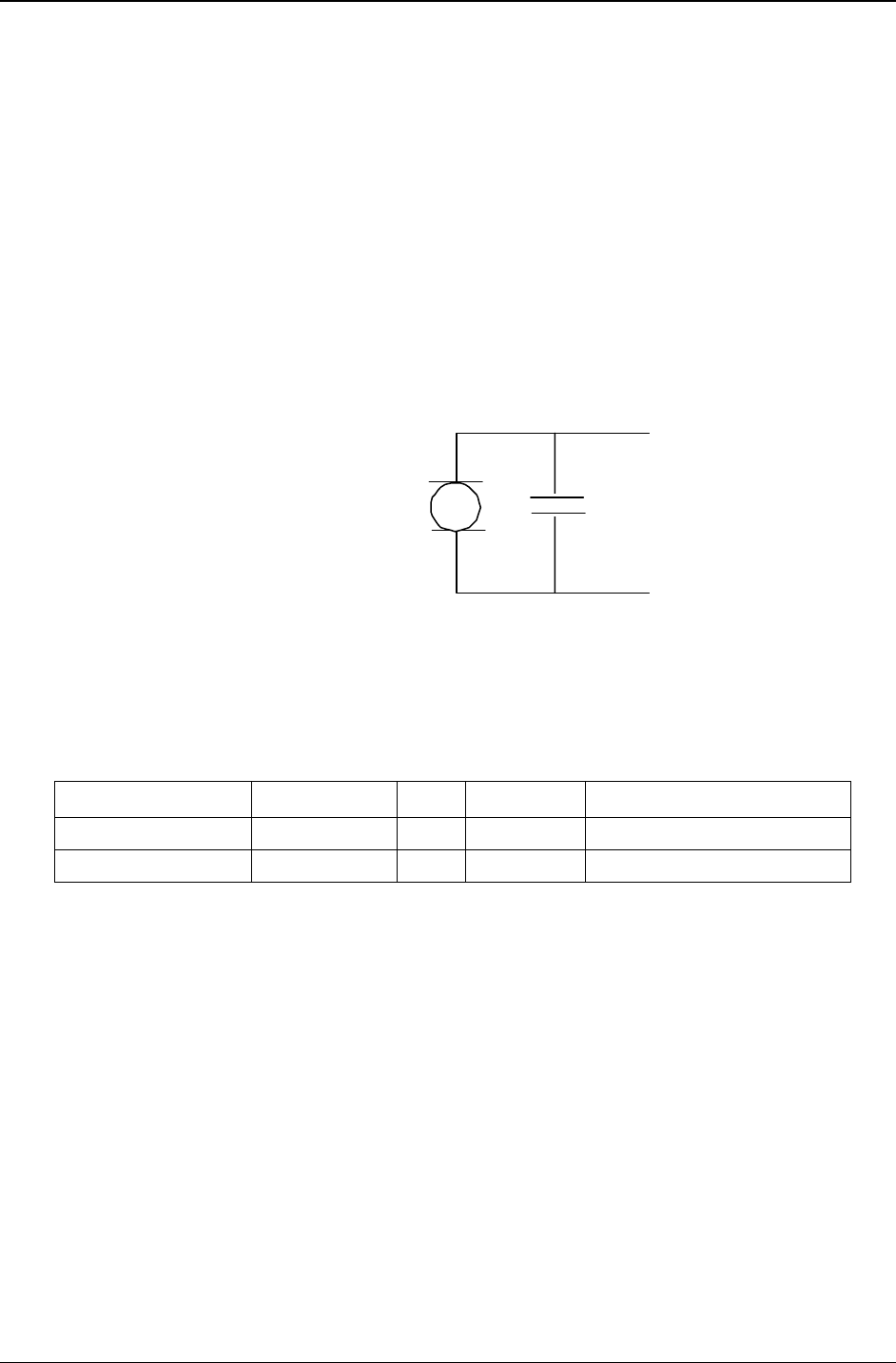
The MIC2 inputs are differential ones. They already include the convenient biasing for an electret microphone
(0,5 mA and 2 Volts). This electret microphone can be directly connected on these inputs. The impedance of the
microphone 2 has to be around 2K. These inputs are the standard ones for a handset design while MIC1 inputs
can be connected to an external headset or a hands-free kit.
The gain of MIC2 inputs is internally adjusted. The gain can be tuned from 30dB to 51dB. The connection to the
microphone is direct. The gain can be tuned using the AT+VGR command. See Appendix B: Sourcing Guide for
Connectors and Peripheral Devices.
MIC2N
MIC2P
C1
C1 = 22pF to 100 pF
33 pF recommended
Figure 3-8: Microphone 2 Input
C1 has to be the nearest as possible to the microphone. Microphone manufacturers provide this capacitor
directly soldered on the microphone.
Table 3-19: Microphone 2 Input Pin Description
Signal Pin Number I/O I/O Type* Description
MIC2P 16 I Analog Microphone 2 positive input
MIC2N 18 I Analog Microphone 2 negative input
* See “Table 3-2: Operating Conditions” in section on the 50-pin Connector Description.
Chapter 3 – Electrical Characteristics
Wireless ModemModule MTMMC-G-F1 and MTMMC-G-F2 Developer’s Guide 26
Microphone 1 Inputs
The MIC1 inputs are differential and do not include internal bias. To use these inputs with an electret
microphone, bias has to be generated outside the ModemModule according to the characteristic of this electret
microphone. These inputs are the standard ones used for an external headset or a hands-free kit. When using a
single-ended connection, be sure to have a very good ground plane, a very good filtering as well as shielding in
order to avoid any disturbance on the audio path. The gain of MIC1 inputs is internally adjusted. The gain can be
tuned from 30dB to 51dB.
The gain can be tuned using the AT+VGR command.
C1
C2
R1
R2
R3
R4
Vcc analog power supply
2.8 V
MIC1P
MIC1N
Differential Connection
Figure 3-9: Microphone 1 Input
R1 = R4 = from 100 to 330 .
R2 = R3 = usually between 1K and 3.3K as per the
microphone characteristics
C1 = 22pF to 100pF
C2 = 47µF
R1 and R4 are used as a voltage supply filter with C2.
C1 has to be the nearest possible to the microphone. Microphone manufacturers provide this capacitor directly
soldered on the microphone.
Table 3-20: Microphone 1 Input Pin Description
Signal Pin Number I/O I/O Type* Description
MIC1P 20 I Analog Microphone 1 positive input
MIC1N 22 I Analog Microphone 1 negative input
* See “Table 3-2: Operating Conditions” in section on the 50-pin Connector Description.
Chapter 3 – Electrical Characteristics
Wireless ModemModule MTMMC-G-F1 and MTMMC-G-F2 Developer’s Guide 27
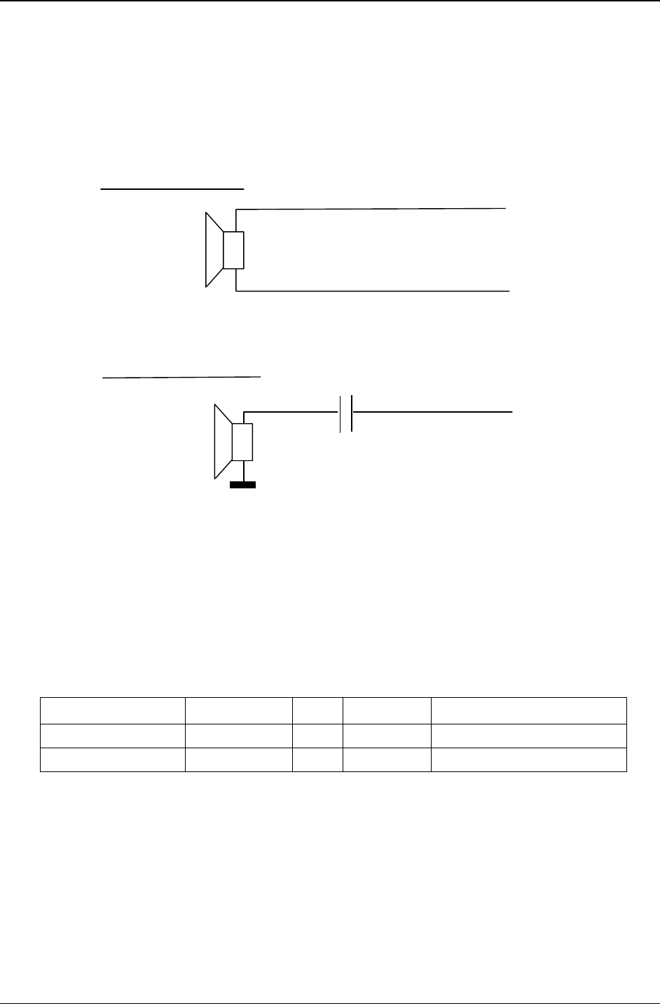
Speaker 2 Outputs
Speaker outputs SPK2 are push-pull amplifiers and can be loaded down to 50 Ohms and up to 1nF. These
outputs are differential and the output power can be adjusted by step of 2dB. The output can be directly
connected to a speaker. When using a single-ended connection, be sure to have a very good ground plane, a
very good filtering as well as shielding in order to avoid any disturbance on the audio path.
SPK2P
+
C1
Differential Connection
SPK2P
SPK2N
Single-Ended Connection
Figure 3-10: Speaker 2 Output
C1 = from 100nF to 47µF as per the speaker characteristics and the output power.
Using a single-ended connection also includes losing half of the output power compared to a differential
connection.
Table 3-21: Speaker 2 Output Pin Description
Signal Pin Number I/O I/O Type* Description
SPK2P 10 O Analog Speaker 2 positive output
SPK2N 8 O Analog Speaker 2 negative output
* See “Table 3-2: Operating Conditions” in section on the 50-pin Connector Description.
Chapter 3 – Electrical Characteristics
Wireless ModemModule MTMMC-G-F1 and MTMMC-G-F2 Developer’s Guide 28
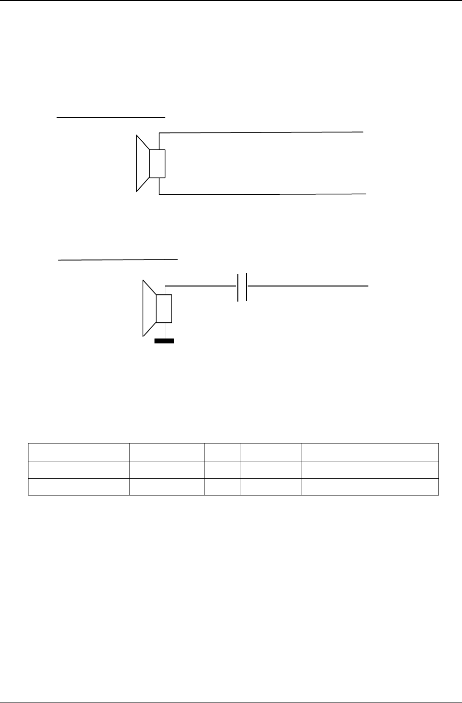
Speaker 1 Outputs
Speaker outputs SPK1 are push-pull amplifiers and can be loaded down to 50 Ohms and up to 1nF. These
outputs are differential and the output power can be adjusted by step of 2dB. The output can be directly
connected to a speaker. When using a single-ended connection, be sure to have a very good ground plane, a
very good filtering as well as a shielding in order to avoid any disturbance on the audio path.
SPK1P
+
C1
Differential Connection
SPK1P
SPK1N
Single-Ended Connection
Figure 3-11: Speaker 1 Output
C1 = from 100nF to 47µF as per the speaker characteristics.
Using a single-ended connection also includes losing half of the output power compared to a differential
connection.
Table 3-22: Speaker 1 Output Pin Description
Signal Pin Number I/O I/O Type* Description
SPK1P 12 O Analog Speaker 1 positive output
SPK1N 13 O Analog Speaker 1 negative output
* See “Table 3-2: Operating Conditions” in section on the 50-pin Connector Description.

Chapter 3 – Electrical Characteristics
Wireless ModemModule MTMMC-G-F1 and MTMMC-G-F2 Developer’s Guide 29
SIM interface
The external SIM interface is available through the 50-pin connector in order to use a stand-alone SIM
cardholder. 5V SIMs can be driven using an external level shifter.
SIM line must not exceed 15 cm. See also the “Hardware and RF” section of Chapter 5: Application
Considerations.
Five signals are available:
SIMVCC: SIM power supply.
SIMRST: reset.
SIMCLK: clock.
SIMDATA: I/O port.
SIMPRES1 SIM card detect. This signal is connected to the external SIM connector on pin 8. Pin 4 of SIM
connector must be pulled down to GND with 1 K.
This interface is fully compliant with GSM 11.11 recommendations concerning the SIM functionality.
Transient Voltage Suppressor diodes are internally added on the signals connected to the SIM socket in order to
prevent any Electro-Static Discharge. TVS diodes with low capacitance (less than 10pF) are connected on
SIMCLK and SIMDATA to avoid any disturbance of the rising and falling edge.
Table 3-23: SIM Interface Pin Description
Signal Pin Number I/O I/O Type* Description
SIMCLK 45 O 2X SIM Clock
SIMRST 46 O 2X SIM Reset
SIMDATA 49 I/O CMOS/2X SIM Data
SIMVCC 47 O SIM Power Supply
SIMPRES1 48 I CMOS SIM Card Detect
GPO0 50 O 2X SIM 3V or 5V
* See “Table 3-2: Operating Conditions” in section on the 50-pin Connector Description.
The SIM schematic appears later in this chapter.

Chapter 3 – Electrical Characteristics
Wireless ModemModule MTMMC-G-F1 and MTMMC-G-F2 Developer’s Guide 30
Table 3-24: SIM Interface Electrical Characteristics
Parameter Conditions Min Typ Max Unit
SIMDATA VIH IIH = +/- 20mA0.7xSIMVCC V
SIMDATA VIL IIL = 1 mA 0.3xSIMVCC V
SIMRST,
SIMDATA
SIMCLK VOH
Source current
= 20mA
SIMVCC – 0.1V V
SIMRST,
SIMDATA
SIMCLK VOL
Sink current
= -200mA
0.1
SIMVCC Output
Voltage
ISIMVCC <= 6mA 2.70 2.80 2.85 V
SIMCLK Rise/Fall
Time
Loaded with
30pF
50 ns
SIMRST,
SIMDATA
Rise/Fall Time
Loaded with
30pF
1ms
SIMCLK
Frequency
Loaded with
30pF
3.25 MHz
Table 3-25: SIM Socket Pin Description
Signal Pin Number Description
Vcc 1 SIMVCC
RST 2 SIMRST
CLK 3 SIMCLK
CC4 4 R10 to Ground
GND 5 Ground
VPP 6 not connected
I/O 7 SIMDATA
CC8 8 SIMPRES1
Chapter 3 – Electrical Characteristics
Wireless ModemModule MTMMC-G-F1 and MTMMC-G-F2 Developer’s Guide 31
GND
SIMVCC
IK
1
SIMRST
SIMCLK
SIMDATA
SIMPRES1 8
7
3
2
VCC
RST
CLK
CC4
GND
VPP
I/O
CC8
Figure 3-12: SIM Socket
SPI Bus
The SPI bus includes a CLK signal, an I/O signal and an EN signal complying with SPI bus standard. The
maximum speed transfer is 3.25Mb/s.
Table 3-26 : SPI Bus Pin Description
Signal Pin Number I/O I/O Type* Description
SPI_CLK 44 O 1X SPI Serial Clock
SPI_IO 43 I/O CMOS/1X SPI Data
SPI_EO 42 O 1X SPI Enable
* See “Table 3-2: Operating Conditions” in section on the 50-pin Connector Description.
Keypad Interface
This interface provides 10 connections: 5 rows (R0 to R4) and 5 columns (C0 to C4).
The scanning is a digital one, and the de-bouncing is done in the integrated modem. No discrete components
like R, C (Resistor, Capacitor) are needed. It is possible to scan the column and rows using the AT+CMER
command. See AT Command manual for more details.
Table 3-27: Keypad Interface Pin Description
Signal Pin Number I/O I/O Type* Description
ROW0 39 I/O CMOS / 1X Row scan
ROW1 40 I/O CMOS / 1X Row scan
ROW2 37 I/O CMOS / 1X Row scan
ROW3 38 I/O CMOS / 1X Row scan
ROW4 35 I/O CMOS / 1X Row scan
COL0 36 I/O CMOS / 1X Column scan
COL1 33 I/O CMOS / 1X Column scan
COL2 34 I/O CMOS / 1X Column scan
COL3 31 I/O CMOS / 1X Column scan
COL4 32 I/O CMOS / 1X Column scan
* See “Table 3-2: Operating Conditions” in section on the 50-pin Connector Description.

Chapter 4 – Interfaces
Wireless ModemModule MTMMC-G-F1 and MTMMC-G-F2 Developer’s Guide 32
Chapter 4 – Interfaces
This chapter describes the ModemModule interfaces.
· Flashing LED
· SIM Interface
· RF Interface
· DTE/DCE Interface Rates
Flashing LED
The flashing LED signal is used to indicate the working mode of the ModemModule.
LED and ModemModule Status
Signal ModemModule Status
OFF Download mode or switched OFF>
Continuously lit Switched ON (not registered on the network)ON
Flashing Switched ON (registered on the network)
SIM Interface
The internal SIM interface of the SocketModule supports 3V SIMs only.
Note: This interface is fully compliant with GSM 11.11 recommendations concerning the SIM functionality.
Five Signals Are Available
SIMVCC: SIM power supply.
SIMRST: reset.
SIMCLK: clock.
SIMDATA: I/O port.
SIMPRES1 SIM card detect.

Chapter 4 – Interfaces
Wireless ModemModule MTMMC-G-F1 and MTMMC-G-F2 Developer’s Guide 33
RF Interface
The impedance is 50 Ohms nominal.
RF Connector
The RF connector is MMCX standard type. An antenna can be directly connected through the matting connector
or using a small adapter.
RF Performances
RF performances are compliant with the ETSI recommendation 05.05 and 11.10.
The main parameters are:
Receiver:
· EGSM Sensitivity : < -104 dBm
· GSM 1800/GSM 1900 Sensitivity : < -102 dBm
· Selectivity @ 200 kHz : > +9 dBc
· Selectivity @ 400 kHz : > +41 dBc
· Dynamic range : 62 dB
· Intermodulation : > -43 dBm
· Co-channel rejection : + 9 dBc
Transmitter:
· Maximum output power (EGSM) : 33 dBm +/- 2 dB
· Maximum output power (DCS/PCS) : 30 dBm +/- 2 dB
· Minimum output power (EGSM): 5 dBm +/- 5 dB
· Minimum output power (DCS/PCS): 0 dBm +/- 5 dB
· H2 level : < -30 dBm
· H3 level : < -30 dBm
· Noise in 925 - 935 MHz : < -67 dBm
· Noise in 935 - 960 MHz : < -79 dBm
· Noise in 1805 - 1880 MHz : < -71 dBm
· Phase error at peak power : < 5 ° RMS
· Frequency error : +/- 0.1 ppm max
DTE/DCE Interface Rates
The table below indicates the anticipated modem-to-computer interface rates for both the 7.2 bits-per-sample
rate and the 8 bits-per-sample rate.
Projected DTE/DCE Interface Rates for 7.2/8K Hz Sample Rates
Bits per Sample
Projected DTE/DCE I/F
Rate @ 7.2K Hz
Projected DTE/DCE I/F
Rate @ 8K Hz Sample Rate
0.50 4800 9600
1 9600 19200
2 19200 19200
3 38400 38400
4 38400 57600
5 57600 57600
6 57600 115200
7 115200 115200
8 115200 115200
9 115200 115200
10 115200 115200
11 115200 115200
12 115200 Fast
13 Fast Fast
Chapter 5 – Test Board
Wireless ModemModule MTMMC-G-F1 and MTMMC-G-F2 Developer’s Guide 34
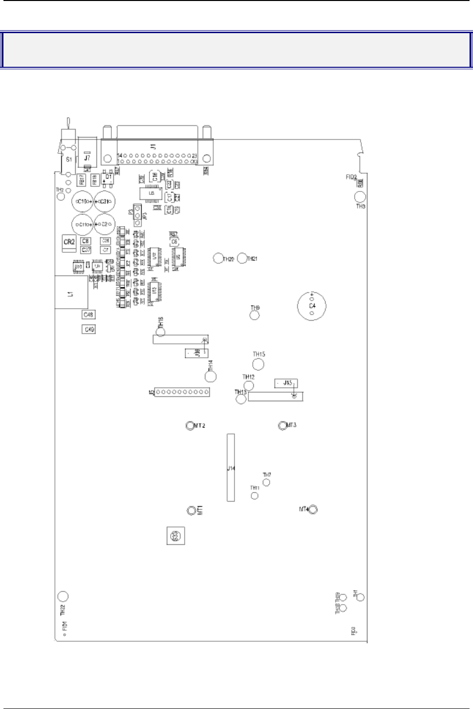
Chapter 5 – Test Board
Serial Test/Demo Board Components
Chapter 5 – Test Board
Wireless ModemModule MTMMC-G-F1 and MTMMC-G-F2 Developer’s Guide 35
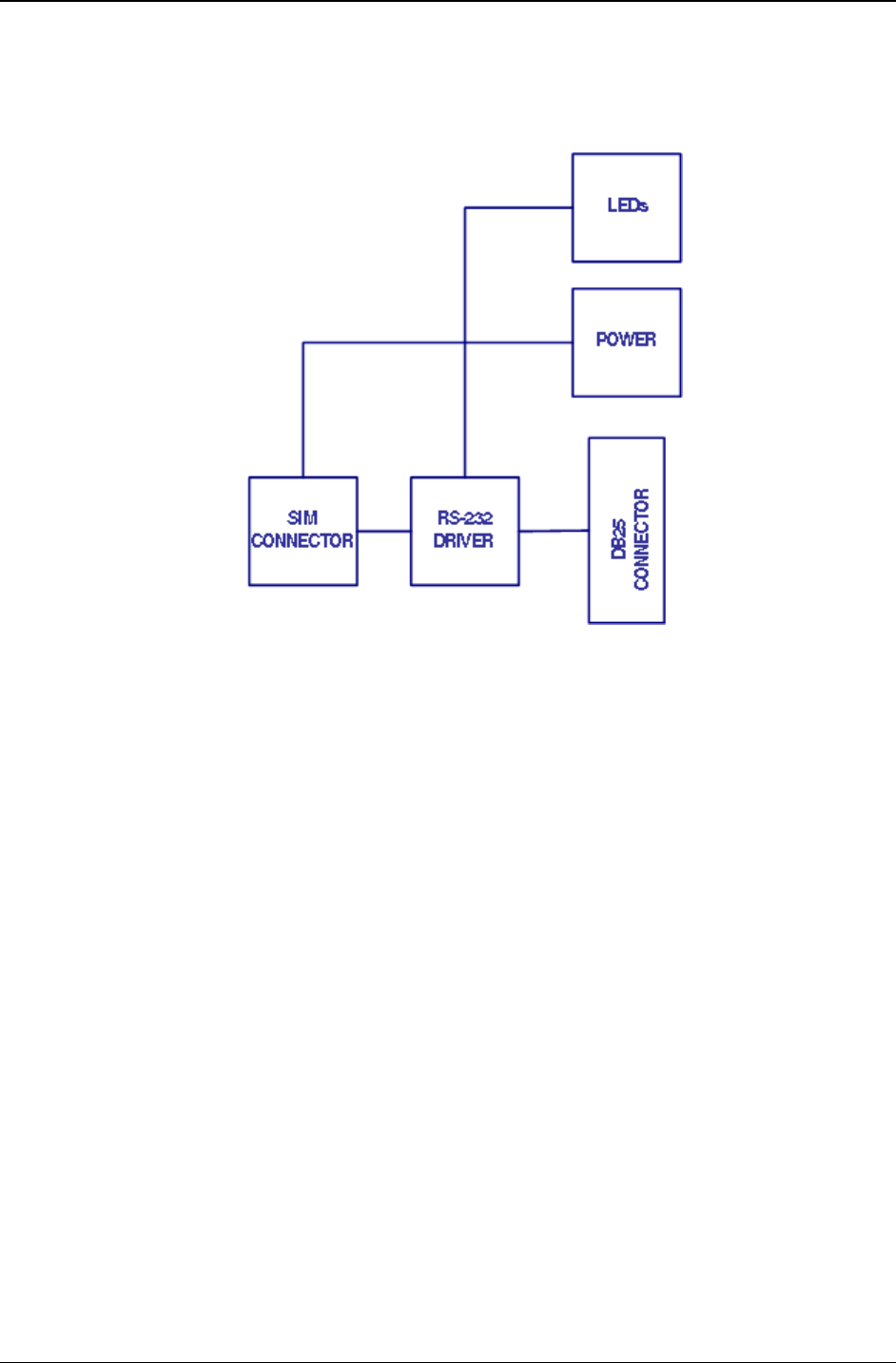
Serial Test/Demo Board Block Diagram
Block Diagram for the ModemModule GSM/GPRS
Chapter 5 – Test Board
Wireless ModemModule MTMMC-G-F1 and MTMMC-G-F2 Developer’s Guide 36
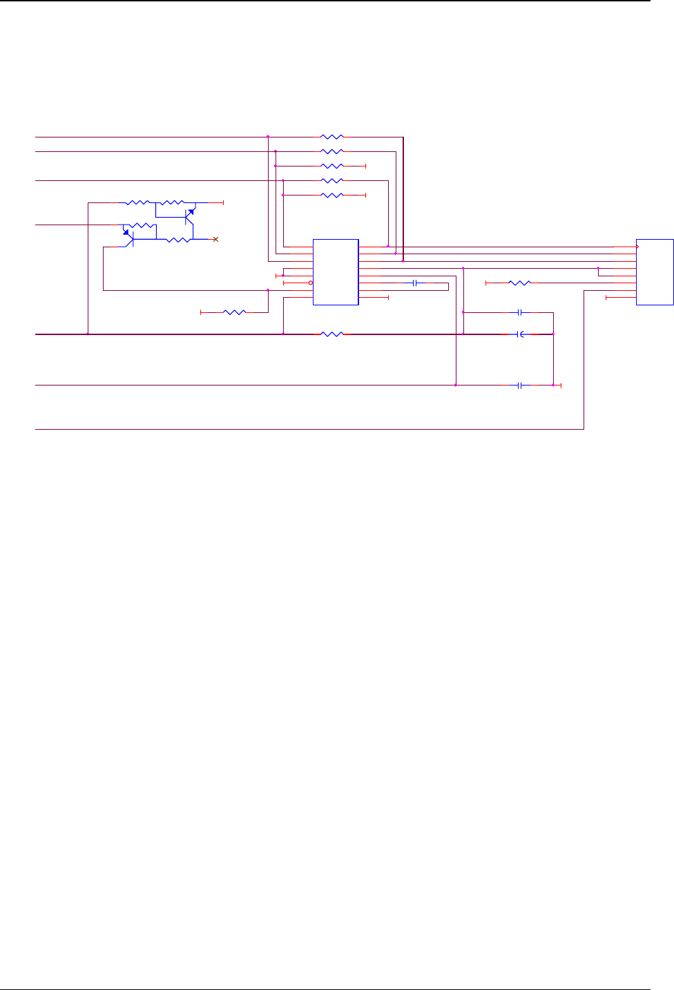
SIM Schematic (5V)
SIM Schematic
GND
VIN = 5V
GND
LTC1555 SIM 3V/5V Level shifter.
GND
VCC = 2.8V
GND
R12 100K
R22 0
U6
LTC1555
8
125
6
7
11
10
9
161
13
215
14
4
3
M0
VINDV CC
SS
M1
C1+
C1-
GND
CLKCIN
VCC
RIN RST
I/O
DDRV
DA TA
Place C30
near pin
13 of U6.
GND
C17 2.2uF
SIMCLK
R21 0
C_GPO0
C43 2.2uFR13 100K
VCC
VIN
GND GND
C28 .1uF
R20, R21, R22 and R23
are used to shunt
LTC1555.
SIM interface from
Modem Module.
+
C30 33uF
R20 0
SIMV CC R23 0
SIMPRES1
GND
4.7K
10K
47K47K
U4
UMC5NT1
1
4
5
3
2
SIMDA TA
J2
SIM_6 P
1
2
3
4
5
6
7
8
VCC
RST
CLK
CC4
GND
VPP
I/0
CC8
R15 1K
GND
SIMRST
R14 100K

Chapter 6 – Application Considerations
Wireless ModemModule MTMMC-G-F1 and MTMMC-G-F2 Developer’s Guide 37
Chapter 6 – Application Considerations
General Guidelines for the Use of the ModemModule
Hardware and RF
· Ground plane: MultiTech recommends having a common ground plane for analog, digital and RF grounds.
· Length of the SIM interface lines (15 cm maximum)
· Bias of the Microphone inputs must be properly adjusted when using audio connectors (mic + speaker) 1.
· EMC protection on audio input/output (filters against 900 MHz)
· ESD protection on serial link, …
· Possible spurious emission radiated by the application to the RF receiver in the receiver band
The Antenna
The antenna sub-system and integration in the application is a major issue. It is a major issue in the choice of the
antenna cable (type, length, performances, thermal resistance, etc.)
These elements could affect GSM performances such as sensitivity and emitted power.
The antenna should be isolated as much as possible from the digital circuitry including the interface signals.
MultiTech recommends shielding the terminal. On terminals including the antenna, a poor shielding could
dramatically affect the sensitivity of the terminal. Subsequently, the power emitted through the antenna could
affect the application.
Firmware Upgrade
The ModemModule firmware is stored in flash memory, and it can easily be upgraded. Contact the factory for
details.
Initial Configuration Using Mobile PhoneTools
For Initial configuration of your wireless device, Multi-Tech offers a Windows-based mobile PhoneTools
application.
To load Mobile PhoneTools, click on the Mobile PhoneTools icon on the system CD and follow the on-screen
prompts.

Chapter 6 – Application Considerations
Wireless ModemModule MTMMC-G-F1 and MTMMC-G-F2 Developer’s Guide 38
Getting Started
Minimum Hardware Interface Required To Get Started
At a minimum, it is necessary to connect the following signals too properly operate the ModemModule:
Table 5-1: Minimum Signals to Operate the ModemModule
Pin Number Name Description
1 GND Ground
2 GND Ground
3 +5V Power Supply
4 +5V Power Supply
6 GND Ground
13 CT106/CTS Clear to Send
15 ON/OFF Power On/Off *
21 GND Ground
24 GND Ground
25 CT103/TX Transmit
28 CT104/RX Receive
30 CT105/RTS Request to Send
* Connected to +5V for example
The serial link signals must be used through the implementation of the serial link level shifter. See “Figure 3-3:
Level Shifter Application Diagram for Serial Link.”
Terminal Emulator Setup
Here below is an example based on the Windows TM Hyperterminal application
(terminal emulator program).
Setup:
1. Go to START – PROGRAMS – ACCESSORIES – HYPERTERMINAL.
2. Start the Hyperterminal software.
3. Give the name of your choice, click on the icon of your choice, and click “OK.”
4. Choose these operating parameter values:
Connect using: direct to COM1
Properties: 115200 bps; 8 bits data; no parity; 1 stop bit; hardware flow control.
5. Click “OK.”
Once Hyperterminal is open and configured, it can be used to send AT commands to the ModemModule.
For assistance in testing your ModemModule, see the examples in the AT Command manual for MultiTech’s
GSM/GPRS wireless modem products (GSM/GPRS AT Commands Reference Guide).

Chapter 6 – Application Considerations
Wireless ModemModule MTMMC-G-F1 and MTMMC-G-F2 Developer’s Guide 39
Reference Documents
Table 5-2: GSM ETSI Recommendations for Phase I and Phase II
Specification Reference Title
GSM ph2 Radio ETSI GSM 05.05 and GT 01 v4.2.1
DCS ph2 Radio ETSI GSM05.05 and GT01 v4.2.1
GSM ph2 Link-Management ETSI GSM 03.06, 04.08, 05.05, 05.08, 05.10, 07.01 an
GT 01 v4.2.1
GSM ph2 Link-Management ETSI GSM 03.06, 04.08, 05.05, 05.08, 05.10, 07.01 an
GT 01 v4.2.1
GSM ph2 Layer 2 ETSI GSM 04.06 and GT 01 v4.2.1
GSM ph2 Layer 3 ETSI GSM 04.08 and GT 01 v4.2.1
DCS ph2 Layer 3 ETSI GSM 04.08 and GT 01 v4.2.1
GSM/DCS Multiband ETSI GSM 02.07, 03.22, 04.08, 04.13, 05.05, 05.08 an
GT 01 v4.2.1
GSM ph2 SIM ETSI GSM 11.11 and GT 01 v4.2.1
GSM ph2 Teleservices ETSI GSM 03.50 and GT 01 v4.2.1
GSM ph2 Miscellaneous ETSI GSM 02.07, 03.40, 03.41, 04.08, 04.10, 04.11,
06.10, 06.11, 06.12, 06.31, 06.32, 07.01, 09.07 and
G 01 v4.2.1
DCS ph2 Miscellaneous ETSI GSM 02.07, 03.40, 03.41, 04.08, 04.10, 04.11,
06.10, 06.11, 06.12, 06.31, 06.32, 07.01, 09.07 and
G 01 v4.2.1
You can find the documents on
ETSI Contacts: ETSI Secretariat
F-06921 Sophia Antipolis cedex, France 06921 Sophia Antipolis cedex, France 06921 Sophia Antipolis cedex,
France 06921 Sophia Antipolis cedex, France
e-mail: secretariat@etsi.fr
http://www.etsi.org
Related Manuals
For information on Multi-Tech modem installation, AT commands, S-Registers, and testing; refer to the
applicable user manual that came with your Multi-Tech modem. Multi-Tech manuals and other resources are on
the Multi-Tech web page at http://www.multitech.com.
For additional Multi-Tech information, contact:
http://www.multitech.com for News, Products, Solutions, Support, Documents and more.
ftp://ftp.multitech.com/ for Modem Firmware, Modem INFs, Manuals, Utilities, etc.
email oemsales@multitech.com for email technical support.

Chapter 6 – Application Considerations
Wireless ModemModule MTMMC-G-F1 and MTMMC-G-F2 Developer’s Guide 40
Additional Information
European Telecommunications Standards Institute (ETSI) - Contact the ETSI at:
650, route des Lucioles
06921 Sophia-Antipolis Cedex
France
Tel: +33 (0)4 92 94 42 00
Fax: +33 (0)4 93 65 47 16
Global Engineering Documents manages a collection of more than one million documents from over 460
organizations worldwide:
http://global.ihs.com
Phone: 800-854-7179
Fax: 303-792-2192
The ITU is the leading publisher of telecommunication technology, regulatory and standard information, with over
4,000 titles in printed form, on CD-ROM and Online at
http://www.itu.int/publications/ .

Appendix A – Safety Precautions & Regulatory Standards Compliance
Wireless ModemModule MTMMC-G-F1 and MTMMC-G-F2 Developer’s Guide 41
Appendix A – Safety Precautions & Regulatory
Standards Compliance
Safety Precautions
IMPORTANT!
FOR THE EFFICIENT AND SAFE OPERATION
OF YOUR GSM INTEGRATED MODEM READ
THIS INFORMATION BEFORE USE.
RF Safety
General
Your ModemModule is based on the GSM standard for cellular technology. The GSM standard is spread all over
the world. It covers Europe, Asia and some parts of America and Africa. This is the most used
telecommunication standard. Your modem is actually a low power radio transmitter and receiver. It sends out
and receives radio frequency energy. When you use your ModemModule integrated modem, the cellular system
that handles your calls controls both the radio frequency and the power level of your cellular modem.
Exposure to RF Energy
There has been some public concern about possible health effects of using GSM modems. Although research on
health effects from RF energy has focused on the current RF technology for many years, scientists have begun
research regarding newer radio technologies, such as GSM. After existing research had been reviewed, and
after compliance to all applicable safety standards had been tested, it has been concluded that the product was
fitted for use. If you are concerned about exposure to RF energy there are things you can do to minimize
exposure. Obviously, limiting the duration of your calls will reduce your exposure to RF energy. In addition, you
can reduce RF exposure by operating your cellular modem efficiently by following the below guidelines.
Efficient Modem Operation
For your modem to operate at the lowest power level, consistent with satisfactory call quality:
· If your modem has an extendible antenna, extend it fully. Some models allow you to place a call with
the antenna retracted. However your modem operates more efficiently with the antenna fully extended.
· Do not hold the antenna when the modem is « IN USE ». Holding the antenna affects call quality and
may cause the modem to operate at a higher power level than needed.
Antenna Care and Replacement
Do not use the modem with a damaged antenna. If a damaged antenna comes into contact with the skin, a minor
burn may result. Replace a damaged antenna immediately. Consult your manual to see if you may change the
antenna yourself. If so, use only a manufacturer-approved antenna. Otherwise, have your antenna repaired by a
qualified technician. Use only the supplied or approved antenna. Unauthorized antennas, modifications or
attachments could damage the modem and may contravene local RF emission regulations or invalidate type
approval.

Appendix A – Safety Precautions & Regulatory Standards Compliance
Wireless ModemModule MTMMC-G-F1 and MTMMC-G-F2 Developer’s Guide 42
General Safety
Driving
Check the laws and the regulations regarding the use of cellular devices in the area where you have to drive as
you always have to comply with them. When using your modem while driving, please: give full attention to
driving, pull off the road and park before making or answering a call if driving conditions so require.
Electronic Devices
Most electronic equipment, for example in hospitals and motor vehicles is shielded from RF energy. However RF
energy may affect some improperly shielded electronic equipment.
Vehicle Electronic Equipment
Check your vehicle manufacturer representative to determine if any on-board electronic equipment is adequately
shielded from RF energy.
Medical Electronic Equipment
Consult the manufacturer of any personal medical devices (such as pacemakers, hearing aids, etc...) to
determine if they are adequately shielded from external RF energy. Turn your modem OFF in health care
facilities when any regulations posted in the area instruct you to do so. Hospitals or health care facilities may be
using RF monitoring equipment.
Aircraft
Turn your modem OFF before boarding any aircraft.
· Use it on the ground only with crew permission.
· Do not use it in the air.
To prevent possible interference with aircraft systems, Federal Aviation Administration (FAA) regulations require
you to have permission from a crewmember to use your modem while the aircraft is on the ground. To prevent
interference with cellular systems, local RF regulations prohibit using your modem while airborne.
Children
Do not allow children to play with your modem. It is not a toy. Children could hurt themselves or others (by
poking themselves or others in the eye with the antenna, for example). Children could damage the modem, or
make calls that increase your modem bills.
Blasting Areas
To avoid interfering with blasting operations, turn your unit OFF when in a « blasting area » or in areas posted: «
turn off two-way radio ». Construction crews often use remote control RF devices to set off explosives.
Potentially Explosive Atmospheres
Turn your modem OFF when in any area with a potentially explosive atmosphere. It is rare, but your modem or
its accessories could generate sparks. Sparks in such areas could cause an explosion or fire resulting in bodily
injuries or even death. Areas with a potentially explosive atmosphere are often, but not always, clearly marked.
They include fueling areas such as petrol stations; below decks on boats; fuel or chemical transfer or storage
facilities; and areas where the air contains chemicals or particles, such as grain, dust, or metal powders. Do not
transport or store flammable gas, liquid, or explosives, in the compartment of your vehicle that contains your
modem or accessories. Before using your modem in a vehicle powered by liquefied petroleum gas (such as
propane or butane) ensure that the vehicle complies with the relevant fire and safety regulations of the country in
which the vehicle is to be used.
Safety Standards
THIS WIRELESS MODEMMODULE COMPLIES WITH ALL APPLICABLE RF SAFETY STANDARDS. This
cellular modem meets the standards and recommendations for the protection of public exposure to RF
electromagnetic energy established by governmental bodies and other qualified organizations, such as the
following:
· Directives of the European Community,
· Directorate General V in Matters of Radio Frequency Electromagnetic Energy

Appendix A – Safety Precautions & Regulatory Standards Compliance
Wireless ModemModule MTMMC-G-F1 and MTMMC-G-F2 Developer’s Guide 43
RF Exposures
Pursuant to 47 CFR § 24.52 of the FCC Rules and Regulations, personal communications services (PCS)
equipment is subject to the radio frequency radiation exposure requirements specified in § 1.1307(b), § 2.1091
and § 2.1093 as appropriate.
The MultiTech ModemModule is a GSM (PCS 1900) terminal which operates in the US licensed PCS frequency
spectrum. The device transmits over the 1850-1910 MHz band and receives over the 1930-1990 MHz Band.
Mult-Tech Systems, Inc. certifies that it has determined that the Modem complies with the RF hazard
requirements applicable to broadband PCS equipment operating under the authority of 47 CFR Part 24, Subpart
E of the FCC Rules and Regulations. This determination is dependent upon installation, operation and use of the
equipment in accordance with all instructions provided.
The Modem is designed for and intends to be used in fixed and mobile applications. "Fixed" means that the
device is physically secured at one location and is not able to be easily moved to another location. "Mobile"
means that the device is designed to be used in other than fixed locations and generally in such a way that a
separation distance of at least 20cm is normally maintained between the transmitter's antenna and the body of
the user or nearby persons. The Modem is not designed for or intends to be used in portable applications (within
20 cm of the body of the user) and such uses are strictly prohibited. To ensure that the unit complies with current
FCC regulations limiting both maximum RF output power and human exposure to radio frequency radiation, a
separation distance of at least 20cm must be maintained between the unit's antenna and the body of the user
and any nearby persons at all times and in all applications and uses. Additionally, in mobile applications,
maximum antenna gain must not exceed 3 dBi (to comply with Section 24.232(b) and is limited to 7 dBi for fixed
applications. Finally, the tune-up procedure for the O9EM2113 ensures that the maximum RF output power of
the device does not exceed 30.0 dBm within the variations that can be expected due to quantity production and
testing on a statistical basis.
Instructions to OEMs
The MultiTech product manual includes specific warnings and cautions in order to ensure that OEMs are aware
of their responsibilities, with regards to RF exposure compliance, for products into which the modem is
integrated. With this guidance, the OEM will be able to incorporate into their documentation the necessary
operating conditions and warnings.
OEMs need to provide a manual with the ‘’final’’ product that clearly states the operating requirements and
conditions and that these must be observed to ensure compliance with current FCC RF exposure requirements /
MPE limits (see the “RF Exposures” section above). This will enable the OEM to generate (and provide the end-
user with) the appropriate operating instructions, warnings and cautions, and/or markings for their product.

Appendix A – Safety Precautions & Regulatory Standards Compliance
Wireless ModemModule MTMMC-G-F1 and MTMMC-G-F2 Developer’s Guide 44
Regulatory Standards Compliance
GSM compliance
Reference regulations: TBR 19, TBR 20, TBR 31, TBR 32.
Table B-1: ModemModule Acceptance Test
Tests Applied Standard Acceptance Criteria
Performance
Test
ETSI recommendation
for GSM/DCS
communication
Full conformity to the recommendation regarding the
main RF parameters.
Cooking Test The test continues even after the Cooking Test
milestone has been reached.
Stress Test Thermal shocks,
IEC 68-2-14.
Full conformity to the recommendation regarding the
main parameters.
Vibration Test Sinusoidal vibration,
IEC 68-2-6.
No performance degradation or mechanical
degradation is allowed after test.
Vibration Test Random vibration,
IEC 68-2-36.
No performance degradation or mechanical
degradation is allowed after test.
Shock Test IEC 68-2-27. No performance degradation or mechanical
degradation is allowed after test.
Bump Test IEC 68-2-29. No performance degradation or mechanical
degradation is allowed after test.
Humidity Test Corrosion test,
IEC68-2-3.
No visible degradation of the product, both visual and
functional.
The unit is tested at room temperature and must be
fully operative for the main RF parameters.
Warehouse
Test
Low temperature
IEC 68-2-1.
Under normal conditions (room temperature) after the
test, the unit must behave in full conformity with the
main RF parameters.
Warehouse
Test
High temperature
IEC 68-2-2.
Under normal conditions (room temperature) after the
test, the unit must behave in full conformity with the
main RF parameters.
Dust Test MIL-STD-810D,
method 510-3.
No visible dust in the visible areas. No more than 50
dust particles in the cabinet of the product. The unit,
tested at room temperature, must be fully operative.
Light Test UV radiation and
temperature EDF
HN60E03.
Visual inspection on the discoloration and other
degradation effects such as cracks I the material of
the unit after test.
Fall Test IEC 68-2-32. Only minor casing degradation is allowed, with a
maximum dimension change of 1mm. The unit must
remain fully operative and fully meet specifications for
the main RF parameters.
Electro Static
Discharge
Test
IEC 100-4-2. No performance degradation allowed after the test.
Salt Mist
Test
IEC 68-2-11. After the test, visual inspection on the unit.
Atmosphere
Test
Flowing mixed gas
corrosion. IEC 68-2-60.
After the test, visual inspection on the unit and inside.
Marking Test EN 60 950 After the test, visual inspection on the unit. No
degradation is allowed on the marking.

Appendix A – Safety Precautions & Regulatory Standards Compliance
Wireless ModemModule MTMMC-G-F1 and MTMMC-G-F2 Developer’s Guide 45
FTA Compliance
The ModemModule has received a Full-Type Approval (according to normal MS requirements) in the
configuration using the internal SIM interface.
IMEI Number
GSM 900/1800:
TAC: 5 000 64
FAC: 11
Serial Numbers: 000000 to 999999
GSM 900/1900:
TAC: 500 100
FAC: 11
Serial Number: 000000 to 999999
GSM/GPRS 900/1800:
TAC: 500161
FAC: 11
Serial Numbers: 000000 to 999999
GSM/GPRS 900/1900:
TAC: 500167
FAC: 11
Serial Number: 000000 to 999999
CE Label
The Wireless ModemModule is CE compliant which implies that the modem is in conformity with the European
Community directives and it bears the CE label.
Carrying out tests:
Electro-magnetic field immunity
EN 61000-4-3
ETS 300-342—1
Radiated emission
EN 55022
ETS 300-342
ESD immunity
EN 61000-4-2
ETS 300-342-1
Appendix B – Sourcing Guide for Connectors/Peripherals
Wireless ModemModule MTMMC-G-F1 and MTMMC-G-F2 Developer’s Guide 46
Appendix B – Sourcing Guide for Connectors and
Peripheral Devices
Where to Find SMD Connectors
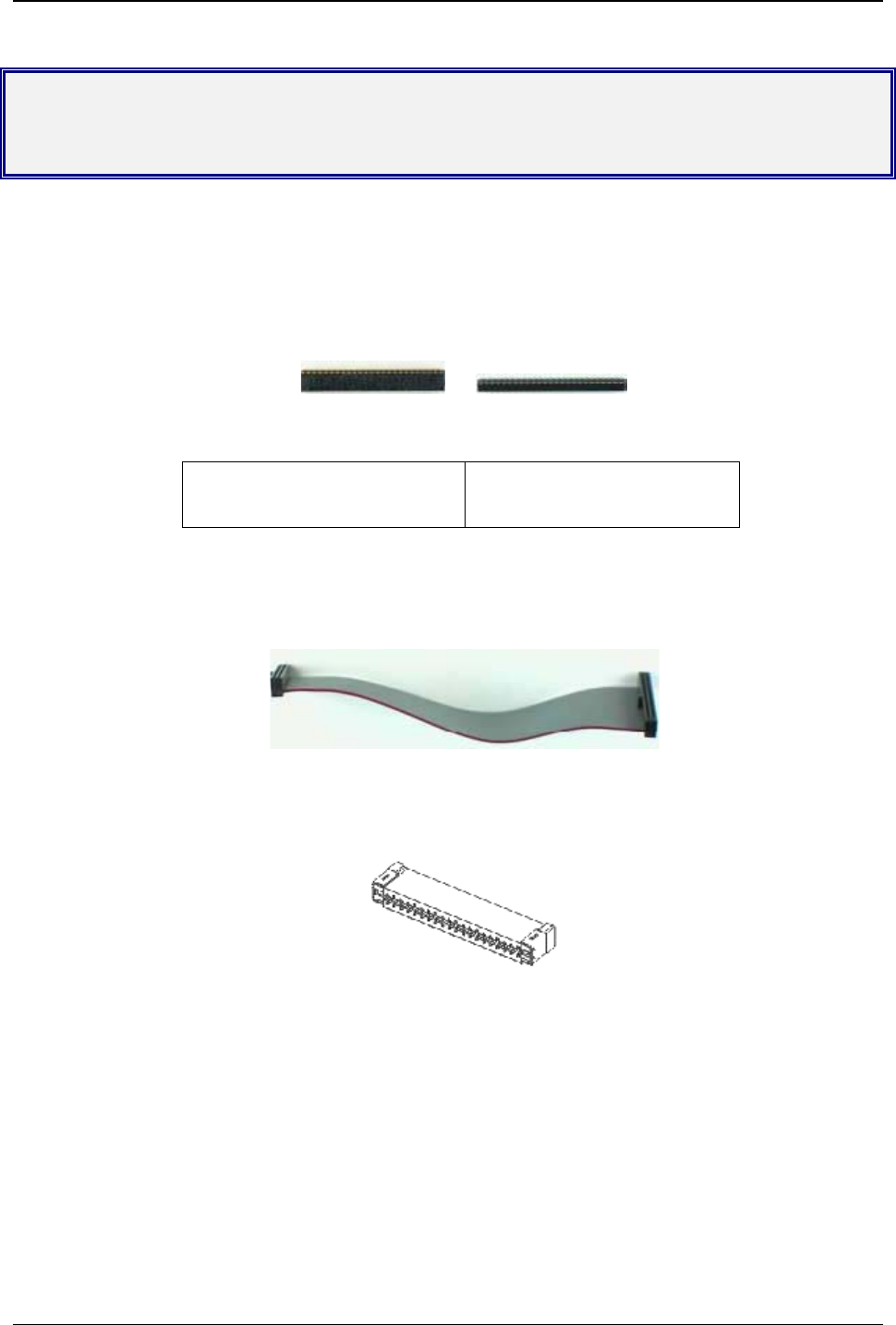
The ModemModule matting interface connector is made by SAMTEC France (http://www.samtec.com/).
Many SAMTEC products are available via SAMTEC dealers throughout the world.
Connector data sheets are presented later in this appendix.
Figure B-1: High- and Low-Profile Connectors
SAMTEC Reference Number for
High-Profile Connector:
FLE-125-01-G-DV
SAMTEC Reference Number for
Low-Profile Connector:
CLP-125-02-L-D
Figure B-2: Flexible Flat Cable
Reference Number for Flexible Flat Cable: SD 25 01 N
Figure B-3: Flexible Cable Receptacle
SAMTEC Reference Number for Flex Cable Connector: FTS-125-01-L-DV-A

Appendix B – Sourcing Guide for Connectors/Peripherals
Wireless ModemModule MTMMC-G-F1 and MTMMC-G-F2 Developer’s Guide 47
GSM Antenna
The integrated modem antenna connector is a MMCX connector. The MMCX connector incorporates a 'Snap On'
latching action in order to make the connection easier with an excellent RF performance. An additional
advantage is its small physical size which is 50% of the standard MCX connector.
This type of connector is suitable for the standard ranges of flexible and semi-rigid cables. The characteristic
impedance of the MMCX coaxial connector is 50 ohm. The antenna manufacturer must guarantee that the
antenna will be working according to the radio characteristics presented in the table below.
Table B-1: Radio Characteristics
GSM 850 EGSM 900 DCS 1800 PCS 1900
Frequency
RX
869 to 894 MHz 925 to 960 MHz 1805 to 1880 MHz 1930 to 990 MHz
Frequency
TX
824 to 849 MHz 880 to 915 MHz 1710 to 1875 MHz 1850 to 910 MHz
RF Power
Stand
2W at 12.5%
duty cycle
2W at 12.5%
duty cycle
1W at 12.5% duty
cycle
1W at 12.5% duty
cycle
Impedance 50 ohms
VSWR <2
Typical
Radiated
Gain
0 dBi on azimuth plane
The ModemModule requires an MMCX plug to connect to an antenna.
Figure B-6: MMCX Connector Example (right angle type)
An antenna with matting connector can be ordered, for example, from :
IMS Connectors Systems GMBH
http://www.imscs.com/
A small MMCX / SMA adapter can be ordered, for example, from :
Amphenol
http://www.amphenol.com/
Order No: 908-31100
SIM Card Holder
The SIM card holder used in the integrated modem is a MOLEX connector.
Part number connector: 99228.
Part number holder : 91236.
For more information about this connector:
http://www.molex.com/
It is possible to use a stand-alone SIM cardholder through the 50-pin connector but the length of the SIM line
must not exceed 15 cm.

Appendix C – AT Command List
Wireless ModemModule MTMMC-G-F1 and MTMMC-G-F2 Developer’s Guide 48
Appendix C – AT Command List
For comprehensive information about AT Commands, please read the AT Command Manual.
Table C-1a : AT Command List
General Commands
+CGMI Manufacturer Identification
+CGMM Request Model Identification
+CGMR Request Revision Identification
+CGSN Product Serial Number
+CSCS Select TE Character Set
+CIMI Request IMSI
+CCID Card Identification
+GCAP Capabilities List
A/ Repeat Last Command
+CPOF Power Off
+CFUN Set Phone Functionality
+CPAS Phone Activity Status
+CMEE Report Mobile Equipment Errors
+CKPD Keypad Control
+CCLK Clock management
+CALA Alarm management

Appendix C – AT Command List
Wireless ModemModule MTMMC-G-F1 and MTMMC-G-F2 Developer’s Guide 49
Table C-1b : AT Command List (cont’d)
Call Control Commands
D Dial command
H Hang-up Command
A Answer a Call
+CEER Extended Error Report
+VTD, +VTS DTMF Signals
ATDL Redial Last Telephone Number
AT%Dn Automatic Dialing (or SMS send) with DTR
ATSO Automatic Answer
+CICB Incoming Call Bearer
+VGR, +VGT Gain Control
+CMUT Microphone Mute Control
+SPEAKER Speaker and Microphone Selection
+ECHO Echo Cancellation
+SIDET Side Tone Modification
+VIP Initialize Voice Parameters
+CSNS Single Numbering Scheme
Network Service Commands
+CSQ Signal Quality
+COPS Operator Selection
+CREG Network Registration
+WOPN Read Operator Name
+CPOL Preferred Operator List
Security Commands
+CPIN Enter PIN
+CPIN2 Enter PIN2
+CPINC PIN Remaining Attempt Number
+CLCK Facility Lock
+CPWD Change Password
Phone Book Commands
+CPBS Select Phone Book Memory Storage
+CPBR Read Phone Book Entries
+CPBF Find Phone Book Entries
+CPBW White Phone Book Entry
+CPBP Phone Book Phone Search
+CPBN Move Action in Phone Book
+CNUM Subscriber Number
+WAIP Avoid Phone Book Init

Appendix C – AT Command List
Wireless ModemModule MTMMC-G-F1 and MTMMC-G-F2 Developer’s Guide 50
Table C-1c: AT Command List (cont’d)
Short Message Commands
+CSMS Select Message Service
+CNMA New Message Acknowledgement
+CPMS Preferred Message Storage
+CMGF Preferred Message Format
+CSAS Save Settings
+CRES Restore Settings
+CSDH Show Text Mode parameters
+CNMI New Message Indication
+CMGR Read Message
+CMGL List Message
+CMGS Send Message
+CMGW Write Message to Memory
+CMSS Send Message from Storage
+CSMP Set Text Mode Parameters
+CMGD Delete Message
+CSCA Service Center Address
+CSCB Select Cell Broadcast Message Types
+WCBM Cell Broadcast Message Identifiers
+WMSC Message Status Modification
+WMGO Message Overwriting
Supplementary Services Commands
+CCFC Call Forwarding
+CLCK Call Barring
+CPWD Modify SS Password
+CCWA Call Waiting
+CLIR Calling Line Identification Restriction
+CLIP Calling Line Identification Presentation
+COLP Connected Line Identification Presentation
+CAOC Advice Of Charge
+CACM Accumulated Call Meter
+CAMM Accumulated Call Meter Maximum
+CPUC Price Per Unit and Currency Table
+CHLD Call Related Supplementary Services
+CLCC List Current Calls
+CSSN Supplementary Service Notifications
+CUSD Unstructured Supplementary Service Data
+CCUG Closed User Group
Data Commands
+CBST Bearer Type Selection
+FCLASS Select Mode
+CR Service Reporting Control
+CRC Cellular Result Codes
+ILRR DTE-DCE Local Rate Reporting
+CRLP Radio Link Protocol Parameters
+DOPT Others Radio Link Parameters
%C Select Data Compression
+DS V42 bis Data Compression
+DR V42 bis Data Compression Report
\N Select Data Error Correcting Mode

Appendix C – AT Command List
Wireless ModemModule MTMMC-G-F1 and MTMMC-G-F2 Developer’s Guide 51
Table C-1d: AT Command List (cont’d)
Fax Commands
+FTM Transmit Speed
+FRM Receive Speed
+FTH HDLC Transmit Speed
+FRH HDLC Receive Speed
+FTS Stop Transmission and Wait
+FRS Receive Silence
Fax Class 2 Commands
+FDT Transmit Data
+FDR Receive Data
+FET Transmit Page Punctuation
+FPTS Page Transfer Status Parameters
+FK Terminate Session
+FBOR Page Transfer Bit Order
+FBUF Buffer Size Report
+FCQ Copy Quality Checking
+FCR Capability to Receive
+FDIS Current Sessions Parameters
+FDCC DCE Capabilities Parameters
+FLID Local ID String
+FPHCTO Page Transfer Timeout Parameter
V24 - V25 Commands
+IPR Fixed DTE Rate
+ICF DTE-DCE Character Framing
+IFC DTE-DCE Local Flow Control
&C Set DCD Signal
&D Set DTR Signal
&S Set DSR Signal
O Back to Online Mode
Q Result Code Suppression
V DCE Response Format
Z Default Configuration
&W Save Configuration
&T Auto-Tests
EEcho
&F Restore Factory Settings
&V Display Configuration
I Request Identification Information
SIM Toolkit Commands
+STSF SIM Toolkit Set Facilities
+STIN SIM Toolkit Indication
+STGI SIM Toolkit Get Information
+STCR SIM Toolkit Control Response
+STGR SIM Toolkit Give Response

Appendix C – AT Command List
Wireless ModemModule MTMMC-G-F1 and MTMMC-G-F2 Developer’s Guide 52
Table C-1e: AT Command List (cont’d)
Specific AT Commands
+CCED Cell Environment Description
+CCED Automatic RxLev Indication
+WIND General Indications
+ADC Analog Digital Converters Measurements
+CMER Mobile Equipment Event Reporting
+WLPR Read Language Preference
+WLPW Write Language Preference
+WIOR Read GPIO Value
+WIOW Write GPIO Value
+WAC Abort Command
+WTONE Play Tone
+WDTMF Play DTMF Tone
+WDWL MultiTech Downloading
+WVR MultiTech Voice Rate
+WDR Data Rate
+WHWV Hardware Version
+WDOP Date Of Production
+WSVG MultiTech Select Voice Gain
+WSTR MultiTech Status Request
+WSCAN MultiTech Scan
+WRIM Ring Indicator Mode
+W32K Power saving mode

Appendix D – Acronyms and Abbreviations
Wireless ModemModule MTMMC-G-F1 and MTMMC-G-F2 Developer’s Guide 53
Appendix D – Acronyms and Abbreviations
ADC : Analog Digital Converter
ASIC : Application Specific Integrated Circuit
BCCH : Broadcast Control Channel
CE : Communauté Européenne
CLK : Clock
CTS : Clear To send
dB : decibel
DCD : Data Carrier Detect
DCE : Data Circuit Terminating Equipment
DSR : Data Set Ready
DTE : Data Terminal Equipment
DTR : Data Terminated Ready
EFR : Enhanced Full Rate
E-GSM : Extended- GSM
EMC : Electromagnetic Conformity
EN : Enable
ETSI : European Telecommunications Standards Institute
FAC : Final Assembly Code
FR : Full-Rate
FTA : Full Type Approval
GND : Ground
GPIO : General Purpose Input Output
GPRS : General Packet Radio Service
GSM : Global System for Mobile Communication
HR : Half-Rate
IMEI : International Mobile Equipment Identity
MO : Mobile Originated
MT : Mobile Terminated
OEM : Original Equipment Manufacturer
PDA : Personal Digital Assistant
PCB : Printed Circuit Board
PRES : Presence
RI : Ring Indicator
RTS : Request To Send
SIM : Subscriber Identity Module
SMD : Surface Mounted Design
SMS : Short Message Service
TAC : Type Approval Code
TDMA : Time Code Multiple Access
TE : Terminal Equipment
VSWR : Voltage Standing Wave Ratio
WAP : Wireless Application Protoc

Appendix D – Acronyms and Abbreviations
Wireless ModemModule MTMMC-G-F1 and MTMMC-G-F2 Developer’s Guide 54
Index
1
1X ....................................................14, 15, 16, 19, 31
2
2X ........................................ 14, 15, 16, 19, 23, 24, 29
3
3X ......................................................................15, 16
A
advice of charge.........................................................8
Advice of Charge.......................................................7
Advice Of Charge....................................................50
analog ............................................................7, 37, 53
antenna...............................7, 8, 33, 37, 41, 42, 43, 47
antenna cable ...........................................................37
asynchronous .........................................................7, 8
AT command ...................................................6, 7, 39
autobauding ...............................................................7
AUXV0..............................................................14, 24
B
baud rate ....................................................................7
BOOT ................................................................14, 22
bursts..................................................................17, 18
C
Call Barring .........................................................7, 50
Call Forwarding...................................................7, 50
Call Hold ...................................................................7
Call Waiting.........................................................7, 50
Calling Line Identity..................................................7
casing.......................................................................44
CE......................................................................45, 53
Cell Broadcast .....................................................6, 50
Class 1 .........................................................5, 6, 7, 12
Class 10 .................................................................5, 6
Closed User Group ..............................................7, 50
CMOS................ 14, 15, 16, 19, 20, 22, 23, 24, 29, 31
column ...............................................................15, 31
connector .................5, 6, 7, 10, 13, 15, 29, 33, 46, 47
converter ..................................................................24
D
data ....................................5, 6, 7, 8, 9, 13, 19, 38, 46
Data Carrier Detect............................................19, 53
dB ................................................................12, 33, 53
DCS .......................................................12, 33, 39, 44
digital.......................................................7, 24, 31, 37
DTE/DCE Interface Rates .......................................33
dual-band ...................................................................5
E
EFR..................................................................6, 8, 53
Electrical Characteristics .........................................13
EMC protection .......................................................37
emergency calls .........................................................8
ESD protection ........................................................37
ETSI.......................................................33, 39, 44, 53
Explicit Call Transfer ................................................7
F
fax..........................................................................5, 7
fixed dialing number..................................................8
FR ....................................................................6, 8, 53
G
gain ..............................................................25, 26, 43
general purpose..................................................13, 15
GND ....................................14, 15, 17, 29, 30, 38, 53
GPIO............................................................24, 52, 53
GPRS ...................................1, 5, 6, 7, 8, 9, 18, 45, 53
ground plane ....................................17, 26, 27, 28, 37
GSM1, 5, 6, 7, 8, 9, 12, 19, 29, 32, 33, 37, 39, 41, 43,
44, 45, 47, 53
H
handset.....................................................................25
hardware ..........................................5, 6, 8, 21, 22, 38
HR ...................................................................6, 8, 53
I
I/O14, 15, 16, 19, 20, 22, 23, 24, 25, 26, 27, 28, 29,
30, 31, 32
idle .....................................................................17, 18
idle mode ...........................................................17, 18
interface ... 5, 6, 7, 8, 13, 15, 19, 29, 31, 32, 37, 45, 46
M
MIC1N...............................................................14, 26
MIC1P ...............................................................14, 26
MIC2N...............................................................14, 25
MIC2P ...............................................................14, 25
microphone ........................................................25, 26
MMCX (Miniature Micro Connector) .......6, 7, 33, 47
MNP2 ........................................................................7
MO.............................................................6, 8, 42, 53
modem ......... 5, 6, 7, 17, 20, 31, 39, 41, 42, 43, 45, 47
module .................................................5, 8, 10, 14, 22
mounting....................................................................6
MT ...................................................................6, 8, 53
multiparty ..................................................................8

Index
Wireless ModemModule MTMMC-G-F1 and MTMMC-G-F2 Developer’s Guide 55
N
nominal value ..........................................................17
O
OFF............................................14, 20, 21, 23, 38, 42
ON/~OFF...........................................................14, 20
operating conditions ................................................43
P
PCB ...................................................................10, 53
PCS....................................................................33, 43
phone book ............................................................7, 8
power6, 8, 13, 17, 21, 22, 27, 28, 29, 32, 33, 37, 41,
43
power supply................................................17, 29, 32
R
radio.......................................................41, 42, 43, 47
real time clock ...........................................................8
RF ................ 5, 7, 8, 10, 13, 33, 37, 41, 42, 43, 44, 47
RST........................................................14, 22, 23, 30
S
serial link .................................................7, 19, 37, 38
signal..........................................20, 22, 23, 29, 31, 32
SIM5, 6, 7, 10, 13, 15, 29, 30, 31, 32, 36, 37, 39, 45,
47, 51, 53
SIM Toolkit .........................................................7, 51
SIMCLK................................................15, 29, 30, 32
SIMDATA.............................................15, 29, 30, 32
SIMPRES ................................................................15
SIMRST.................................................15, 29, 30, 32
SIMVCC................................................15, 29, 30, 32
SMS .......................................................5, 6, 8, 49, 53
socket.............................................................6, 15, 29
speaker...................................................25, 27, 28, 37
Specifications
technical ...............................................................10
SPI .....................................................................15, 31
SPK1N...............................................................14, 28
SPK1P ...............................................................14, 28
T
Technical specifications...........................................10
telephony ...................................................................8
terminal..................................................19, 37, 38, 43
U
UCS2 .........................................................................7
USSD.....................................................................7, 8
V
V.42bis ......................................................................7
Vcc.....................................................................14, 30
voice ..........................................................................5
W
WAP ........................................................................53
X
Xmodem ....................................................................7

Index
Wireless ModemModule MTMMC-G-F1 and MTMMC-G-F2 Developer’s Guide 56
LIST OF FIGURES
Figure 1-1: MultiTech’s Wireless ModemModule GSM/GPRS 5
Figure 1-2: Mechanical Description A 10
Figure 1-3: Mechanical Description B 10
Figure 2-1: ModemModule Dimensions 11
Figure 3-1: 50-Pin Connector 16
Figure 3-2: Pin Numbering – Bottom View 17
Figure 3-3: Level Shifter Application Diagram for Serial Link 20
Figure 3-4: Power-Off Procedure 1 21
Figure 3-5: Power-Off Procedure 2 21
Figure 3-6: Boot Procedure 22
Figure 3-7: Reset Procedure 22
Figure 3-8: Microphone 2 Input 25
Figure 3-9: Microphone 1 Input 26
Figure 3-10: Speaker 2 Output 27
Figure 3-11: Speaker 1 Output 28
Figure 3-12: SIM Socket 31
Figure 3-13: SIM Schematic 36
Figure 4-1: ModemModule Test SM Card Layout Error! Bookmark not defined.
Figure 4-2: ModemModule Test SM Board Block Diagram Error! Bookmark not defined.
Figure B-1: High- and Low-Profile Connectors 46
Figure B-2: Flexible Flat Cable 46
Figure B-3: Flexible Cable Receptacle 46
Figure B-4: Samtec Low-Profile Sockets Error! Bookmark not defined.
Figure B-5: Samtec Cable Strips Error! Bookmark not defined.
Figure B-6: MMCX Connector Example (right angle type) 47

Index
Wireless ModemModule MTMMC-G-F1 and MTMMC-G-F2 Developer’s Guide 57
LIST OF TABLES
Table 2-1 : Climatic and Mechanical Environment Testing Compliance 12
Table 3-1a. 50-pin Connector Description 14
Table 3-1b. 50-Pin Connector Description 15
Table 3-2. Operating Conditions 16
Table 3-3: Power Supply Pin Description 17
Table 3-4: Power Consumption in EGSM-only mode @25 degrees C 17
Table 3-5: Power Consumption in GSM-only 1800 & 1900 MHz modes @25 degrees C 18
Table 3-6: Power Consumption in EGSM/GPRS cl2 mode @25 degrees C 18
Table 3-7: Power Consumption in EGSM-only mode @25 degrees C 18
Table 3-8: Serial Link Pin Description 19
Table 3-9: ON / OFF Pin Description 20
Table 3-10: BOOT Pin Description 22
Table 3-11: Reset Signal Pin Description 23
Table 3-12: Reset Signal Electrical Characteristics 23
Table 3-13: Reset Signal Operating Conditions 23
Table 3-14 : Flashing LED Pin Description 23
Table 3-15 : LED and ModemModule Status 23
Table 3-16 : General Purpose I/O Pin Description 24
Table 3-17: A/D Converter Pin Description 24
Table 3-18: A/D Converter Electrical Characteristics 24
Table 3-19 : Microphone 2 Input Pin Description 25
Table 3-20 : Microphone 1 Input Pin Description 26
Table 3-21 : Speaker 2 Output Pin Description 27
Table 3-22 : Speaker 1 Output Pin Description 28
Table 3-23: SIM Interface Pin Description 29
Table 3-24: SIM Interface Electrical Characteristics 30
Table 3-25: SIM Socket Pin Description 30
Table 3-26 : SPI Bus Pin Description 31
Table 3-27 : Keypad Interface Pin Description 31
Table 5-1: Minimum Signals to Operate the ModemModule 38
Table 5-2: GSM ETSI Recommendations for Phase I and Phase II 39
Table B-1 : ModemModule Acceptance Test 44
Table B-1: Radio Characteristics 47
Table C-1a : AT Command List 48
Table C-1b : AT Command List (cont’d) 49
Table C-1c: AT Command List (cont’d) 50
Table C-1d: AT Command List (cont’d) 51
Table C-1e: AT Command List (cont’d) 52