InnoComm Mobile Technology BM10-AN BT4.0 LE Module User Manual
InnoComm Mobile Technology Corporation BT4.0 LE Module
User Manual.pdf

BT4.0 LE Module
User Manual
Model name: BM10_AN

Introduction
This document describes Key feature, pin definition, mechanical drawing,
Recommendation for PCB Layout and operation temperature and voltage range, and
reflow data of Bluetooth Low Energy Module and it can helps designer to design in
easier and manufacturing smoothly.
BLE module Install Guide line
Key Features
RF
• 2.4-GHz Bluetooth low energy Compliant and Proprietary RF Single Mode Module
• Supports 250-kbps, 500-kbps, 1-Mbps, 2-Mbps Data Rates
• Software programmable adjustable transmitter power (-20dBm to 5dBm) for short
to long range applications
• Suitable for Systems Targeting Compliance With Worldwide Radio Frequency
Regulations: ETSI EN 300 328 and EN 300 440 Class 2 (Europe), FCC CFR47
Part 15 (US), and ARIB STD-T66 (Japan)
Layout
• Few External Components
• 25.45 mm × 16.7 mm × 2 mm, 40 pin LCC Package
Low Power
• Wide supply voltage range : 1.8 – 3.8V
• Differential RF mode : 6.4±3 mA
• Differential RF mode TX at 0 dBm: 6.8±3 mA
• Differential RF mode TX at +5 dBm: 8.9±3mA
• Low Power Mode: 1 μA (RTC Running + RAM/CPU retention)
• Low Power Mode: 100 nA (Flash retention)
• Optional on-chip DC/DC converter (not available in 1.8V mode)
Peripherals
• Integrated temperature sensor
• 4 General-purpose Timer Modules (8x 16-bit or 4x 32 bit-timer, PWM each)
• 12-bit ADC, 200 ksamples/s, 8 channel analog MUX

• Ultra-low-power analog comparator
• UART
• 2x SPI
• Ultra-low power
• I2C, I2S
• Real-time clock
• AES-128 security module
• Support for 8 capacitive sensing channels
Application Profile
• Consumer electronics
• Mobile phone accessories
• Sports & Fitness equipment
• HID applications
• Home and Building Automation
• Lighting Control
• Alarm and Security
• Electronic Shelf Labeling
• Proximity Tags
• Medical
• Remote Controls
• Wireless Sensor Networks
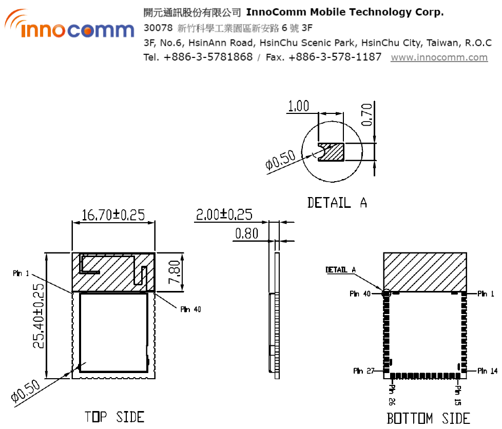
Mechanical Drawing
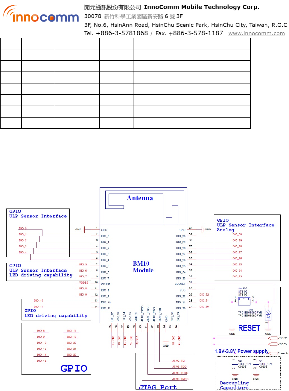
Module Pin Definition
Bluetooth Module
Pin # Pin Name Direction Voltage Description
1 GND Power GND Ground
2 DIO_0 Digital I/O 1.8V to 3.8V
GPIO, ULP Sensor Interface
3 DIO_1 Digital I/O 1.8V to 3.8V
GPIO, ULP Sensor Interface
4 DIO_2 Digital I/O 1.8V to 3.8V
GPIO, ULP Sensor Interface
5 DIO_3 Digital I/O 1.8V to 3.8V
GPIO, ULP Sensor Interface
6 DIO_4 Digital I/O 1.8V to 3.8V
GPIO, ULP Sensor Interface
7 DIO_5 Digital I/O 1.8V to 3.8V
GPIO, ULP Sensor Interface, LED driving capability
8 DIO_6 Digital I/O 1.8V to 3.8V
GPIO, ULP Sensor Interface, LED driving capability
9 DIO_7 Digital I/O 1.8V to 3.8V
GPIO, ULP Sensor Interface, LED driving capability
10 VDDS2 Power 1.8V to 3.8V
1.8V – 3.8V DIO supply
11 DIO_8 Digital I/O 1.8V to 3.8V
GPIO
12 DIO_9 Digital I/O 1.8V to 3.8V
GPIO
13 DIO_10 Digital I/O 1.8V to 3.8V
GPIO, LED driving capability
14 DIO_11 Digital I/O 1.8V to 3.8V
GPIO, LED driving capability
15 DIO_12 Digital I/O 1.8V to 3.8V
GPIO
16 DIO_13 Digital I/O 1.8V to 3.8V
GPIO
17 DIO_14 Digital I/O 1.8V to 3.8V
GPIO
18 DIO_15 Digital I/O 1.8V to 3.8V
GPIO
19 VDDS3 Power 1.8V to 3.8V
1.8V – 3.8V DIO supply
20 JTAG_TMSC
Digital I/O 1.8V to 3.8V
JTAG_TMSC
21 JTAG_TCKC
Digital I/O 1.8V to 3.8V
JTAG_TCKC
22 JTAG_TDO Digital I/O 1.8V to 3.8V
GPIO, JTAG_TDO
23 JTAG_TDI Digital I/O 1.8V to 3.8V
GPIO, JTAG_TDI
24 GND Power GND Ground
25 DIO_18 Digital I/O 1.8V to 3.8V
GPIO
26 DIO_19 Digital I/O 1.8V to 3.8V
GPIO
27 DIO_20 Digital I/O 1.8V to 3.8V
GPIO
28 DIO_21 Digital I/O 1.8V to 3.8V
GPIO
29 DIO_22 Digital I/O 1.8V to 3.8V
GPIO
30 VDD Power 1.8V to 3.8V
1.8V – 3.8V main chip supply
31 nRESET I 1.8V to 3.8V
Reset, active-low. No internal pull-up
32 DIO_23 Digital/Analog I/O
1.8V to 3.8V
GPIO, ULP Sensor Interface, Analog
33 DIO_24 Digital/Analog I/O
1.8V to 3.8V
GPIO, ULP Sensor Interface, Analog
34 DIO_25 Digital/Analog I/O
1.8V to 3.8V
GPIO, ULP Sensor Interface, Analog
35 DIO_26 Digital/Analog I/O
1.8V to 3.8V
GPIO, ULP Sensor Interface, Analog
36 DIO_27 Digital/Analog I/O
1.8V to 3.8V
GPIO, ULP Sensor Interface, Analog
37 DIO_28 Digital/Analog I/O
1.8V to 3.8V
GPIO, ULP Sensor Interface, Analog
38 DIO_29 Digital/Analog I/O
1.8V to 3.8V
GPIO, ULP Sensor Interface, Analog
39 DIO_30 Digital/Analog I/O
1.8V to 3.8V
GPIO, ULP Sensor Interface, Analog
40 GND Power GND Ground
Reference Circuit for User design
Recommended: Operating Range
over operating free-air temperature range (unless otherwise noted)
MIN NOM MAX UNIT
Operating ambient temperature range, TA –40 85 °C
Operating supply voltage 1.8 3.8 V
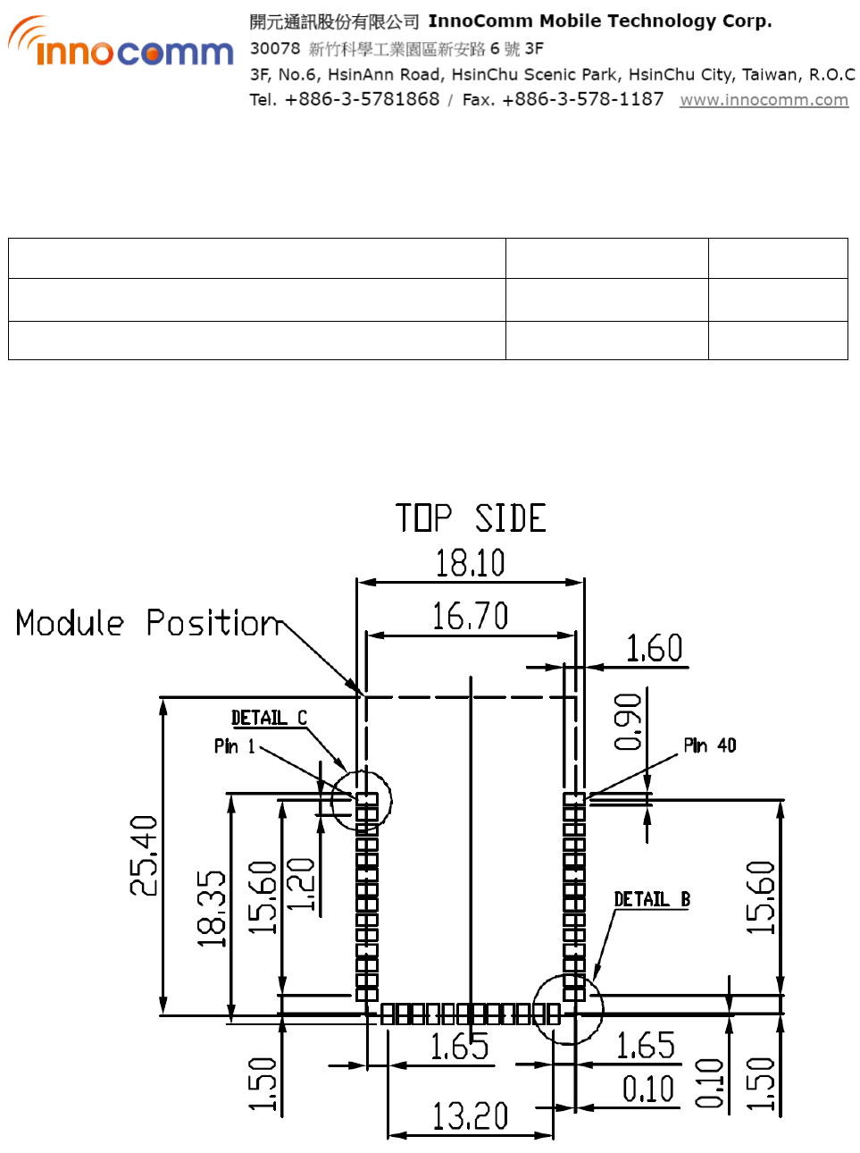
Recommendation: PCB Layout for User design
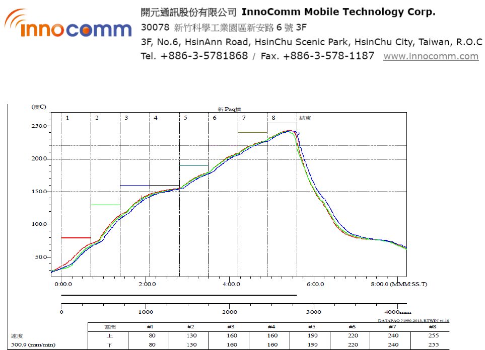
Reflow data

Federal Communication Commission Interference Statement
This device complies with Part 15 of the FCC Rules. Operation is subject to the
following two conditions: (1) This device may not cause harmful interference,
and (2) this device must accept any interference received, including interference
that may cause undesired operation.
This equipment has been tested and found to comply with the limits for a Class
B digital device, pursuant to Part 15 of the FCC Rules. These limits are
designed to provide reasonable protection against harmful interference in a
residential installation. This equipment generates, uses and can radiate radio
frequency energy and, if not installed and used in accordance with the
instructions, may cause harmful interference to radio communications.
However, there is no guarantee that interference will not occur in a particular
installation. If this equipment does cause harmful interference to radio or
television reception, which can be determined by turning the equipment off and
on, the user is encouraged to try to correct the interference by one of the
following measures:
- Reorient or relocate the receiving antenna.
- Increase the separation between the equipment and receiver.
- Connect the equipment into an outlet on a circuit different from that
to which the receiver is connected.
- Consult the dealer or an experienced radio/TV technician for help.
FCC Caution: Any changes or modifications not expressly approved by the party
responsible for compliance could void the user's authority to operate this
equipment.
This transmitter must not be co-located or operating in conjunction with any
other antenna or transmitter.
Radiation Exposure Statement:
The product comply with the FCC portable RF exposure limit set forth for an
uncontrolled environment and are safe for intended operation as described in
this manual. The further RF exposure reduction can be achieved if the product
can be kept as far as possible from the user body or set the device to lower
output power if such function is available.
This device is intended only for OEM integrators under the following conditions:
1) The transmitter module may not be co-located with any other transmitter or
antenna.
As long as 1 condition above is met, further transmitter test will not be required.
However, the OEM integrator is still responsible for testing their end-product for
any additional compliance requirements required with this module installed
IMPORTANT NOTE: In the event that these conditions can not be met (for
example certain laptop configurations or co-location with another transmitter),
then the FCC authorization is no longer considered valid and the FCC ID can not
be used on the final product. In these circumstances, the OEM integrator will be
responsible for re-evaluating the end product (including the transmitter) and
obtaining a separate FCC authorization.
End Product Labeling
The product can be kept as far as possible from the user body or set the device
to lower output power if such function is available. The final end product must
be labeled in a visible area with the following: “Contains FCC ID: YAIBM10-AN ”.
The grantee's FCC ID can be used only when all FCC compliance requirements
are met.
Manual Information To the End User
The OEM integrator has to be aware not to provide information to the end user
regarding how to install or remove this RF module in the user’s manual of the
end product which integrates this module.
The end user manual shall include all required regulatory information/warning
as show in this manual.