Insigma BTIN00 nRF52 Base BLE module User Manual
Insigma inc nRF52 Base BLE module
UserManual.wiki
>
Insigma
>
BTIN00 User Manual
User Manual
Navigation menu
Upload a User Manual
Namespaces
Wiki Guide
HTML
PDF
Info
Views
User Manual
Discussion / Help
Navigation
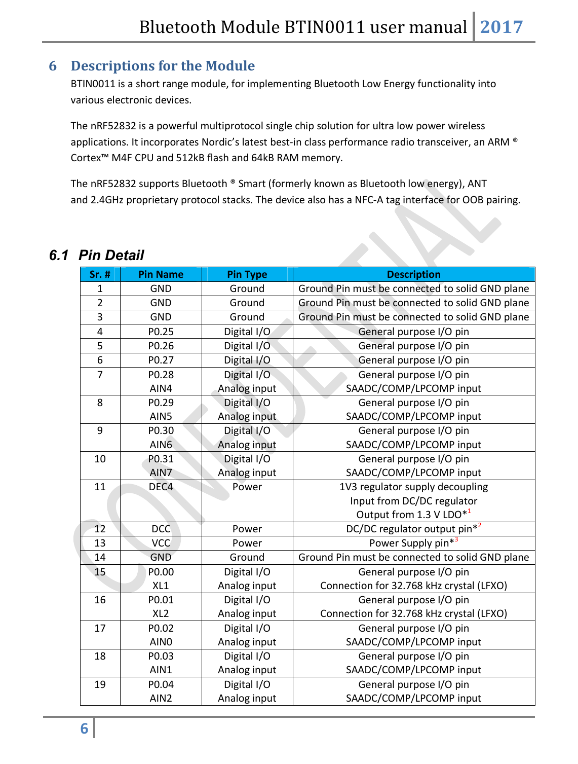
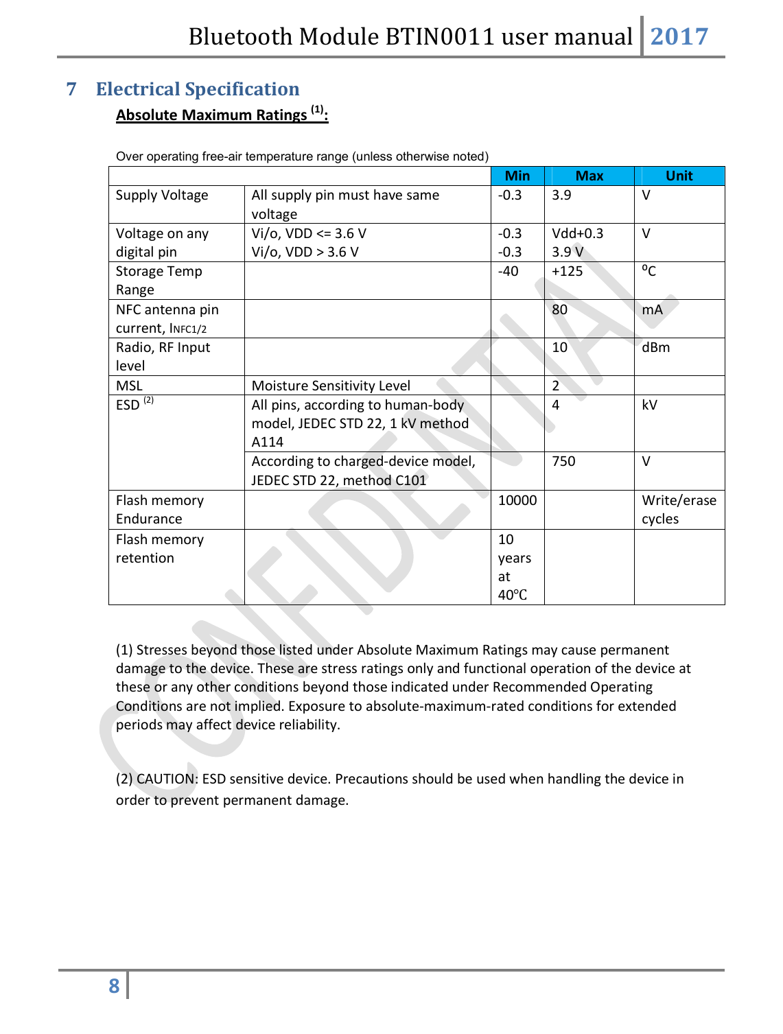
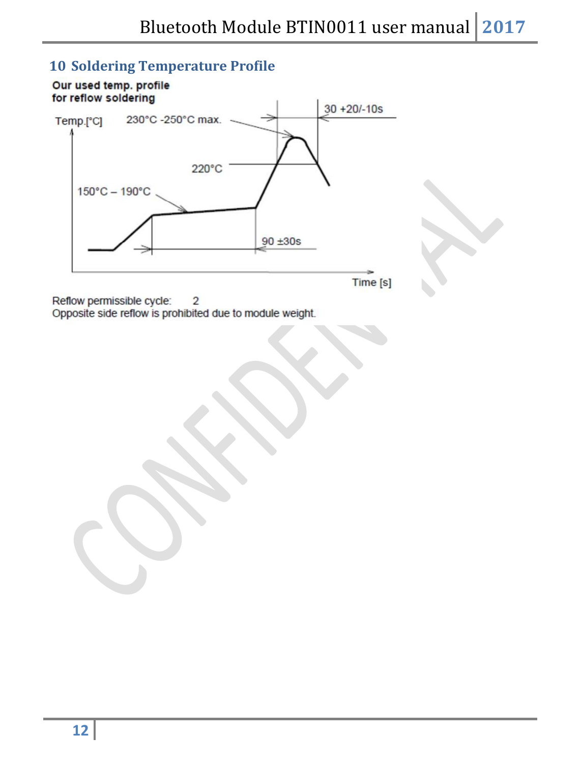
![Bluetooth Module BTIN0011 user manual 2017 7 20 P0.05 AIN3 Digital I/O Analog input General purpose I/O pin SAADC/COMP/LPCOMP input 21 P0.06 Digital I/O General purpose I/O pin 22 P0.07 Digital I/O General purpose I/O pin 23 P0.08 Digital I/O General purpose I/O pin 24 P0.09 NFC1 Digital I/O NFC input General purpose I/O pin NFC antenna connection 25 P0.10 NFC2 Digital I/O NFC input General purpose I/O pin NFC antenna connection 26 GND Ground Ground Pin must be connected to solid GND plane 27 P0.11 Digital I/O General purpose I/O pin 28 P0.12 Digital I/O General purpose I/O pin 29 P0.13 Digital I/O General purpose I/O pin 30 P0.14 TRACEDATA[3] Digital I/O General purpose I/O pin Trace port output 31 P0.15 TRACEDATA[2] Digital I/O General purpose I/O pin Trace port output 32 P0.16 TRACEDATA[1] Digital I/O General purpose I/O pin Trace port output 33 P0.17 Digital I/O General purpose I/O pin 34 P0.18 TRACEDATA[0] SWO Digital I/O General purpose I/O pin Trace port output Single Wire output 35 P0.19 Digital I/O General purpose I/O pin 36 P0.20 TRACECLK Digital I/O General purpose I/O pin Trace port clock output 37 P0.21 RESET Digital I/O General purpose I/O pin Configurable as pin reset 38 SWDCLK Digital input Serial Wire Debug clock input for debug and programming 39 SWDIO Digital I/O Serial Wire Debug I/O for debug and programming 40 P0.22 Digital I/O General purpose I/O pin 41 P0.23 Digital I/O General purpose I/O pin 42 P0.24 Digital I/O General purpose I/O pin 43 GND Ground Ground Pin must be connected to solid GND plane Note: 1) Use 1 F capacitor to ground at DEC4 pin number 11. 2) Use 0.1 F capacitor to ground at VCC pin number 13. 3) Use 15 H, 10 H at DCC pin number 12 for DC/DC Regulator setup.](https://usermanual.wiki/Insigma/BTIN00/User-Guide-3300451-Page-7.png)