User Manual

INSIGMA INC
Bluetooth Module
BTIN0011 user manual
User manual
Ravi Chaudhari
1/23/2017

Bluetooth Module BTIN0011 user manual
2017
2
Contents
1 Purpose ........................................................................................................................................... 3
2 Definition(s) and Abbreviation(s) ..................................................................................................... 3
Quad Flat No-leads / Wafer Level Chip Scale Package...................................................................... 3
3 Reference(s) .................................................................................................................................... 3
4 Key Features .................................................................................................................................... 4
5 Applications for the Module ............................................................................................................ 5
6 Descriptions for the Module ............................................................................................................ 6
6.1 Pin Detail ................................................................................................................................. 6
7 Electrical Specification ..................................................................................................................... 8
8 Mechanical Specification ............................................................................................................... 10
9 Regulatory Statement .................................................................................................................... 11
9.1 FCC Statement: ..................................................................................................................... 11
9.2 FCC Caution: ......................................................................................................................... 11
9.3 FCC Radiation Exposure Statement: .................................................................................... 11
10 Soldering Temperature Profile ................................................................................................... 12
11 Document History ...................................................................................................................... 13
Bluetooth Module BTIN0011 user manual
2017
3
1 Purpose
- This product specification document describes the Insigma Inc. make Nordic Semiconductor
nRF52832 based, Bluetooth Low Energy module.
2 Definition(s) and Abbreviation(s)
Name Abbreviation
BLE
Bluetooth Low Energy
ARM
Advanced RISC Machines
RAM
Random Access Memory
RSSI
Received signal strength indicator
FIFO
First in- first out
DMA
Direct memory access
SPI
Serial Peripheral Interface
UART
Universal Asynchronous Receiver Transmitter
PDM
Pulse density modulation
ECB
electronic codebook
AAR
Accelerated address resolver
QFN/WLCSP
Quad Flat No-leads / Wafer Level Chip Scale Package
IoT
Internet of Things
OOB
Out of Band
SAADC
Successive approximation analog-todigital
COMP
Comparator
LPCOMP
Low power comparator
LFXO
low frequency crystal oscillator
NFC
Near Filed Communication
ESD
Electrostatic Discharge
LDO
Low Dropout
GFSK
Gaussian Frequency Shift Keying
3 Reference(s)
Document No. Title
1 nRF52832_v1.0.pdf

Bluetooth Module BTIN0011 user manual
2017
4
4 Key Features
Multi-protocol 2.4GHz radio
32-bit ARM Cortex M4F processor, 512kB flash + 64kB RAM
Software stacks available as downloads
Application development independent from protocol stack
On-air compatible with nRF51, nRF24AP and nRF24L Series
Programmable output power from +4dBm to -20dBm
RSSI
RAM mapped FIFOs using Easy DMA
Dynamic on air payload length up to 256 Bytes
Flexible and configurable 32 pin GPIO
Programmable Peripheral Interface – PPI
Simple ON/OFF global power modes
Full set of digital interfaces including: SPI/2-wire/UART/PDM/
I2S, all with Easy DMA
12-bit/200KSPS ADC
128-bit AES ECB/CCM/AAR co-processor
Quadrature demodulator
Low cost external crystal 32MHz ± 40ppm for Bluetooth,
± 50ppm for ANT
Low power 32MHz crystal and RC oscillators
Ultra low-power 32kHz crystal and RC oscillators
Wide supply voltage range (1.7 V to 3.6 V)
On-chip DC/DC buck converter
Individual power management for all peripherals
Package options: 48-pin 6x6 QFN/WL-CSP

Bluetooth Module BTIN0011 user manual
2017
5
5 Applications for the Module
All Embedded Wireless Applications
IoT
- Home automation
- Sensor networks
- Building automation
Personal Area Networks
- Health/fitness sensor and monitor devices
- Medical devices
- Key-fobs + wrist watches
Interactive entertainment devices
- Remote control
- Gaming controller
Beacons
A4WP wireless chargers and devices
Remote control toys
Computer peripherals and I/O devices
- Mouse
- Keyboard
- Multi-touch track pad
Bluetooth Module BTIN0011 user manual
2017
6
6 Descriptions for the Module
BTIN0011 is a short range module, for implementing Bluetooth Low Energy functionality into
various electronic devices.
The nRF52832 is a powerful multiprotocol single chip solution for ultra low power wireless
applications. It incorporates Nordic’s latest best-in class performance radio transceiver, an ARM ®
Cortex™ M4F CPU and 512kB flash and 64kB RAM memory.
The nRF52832 supports Bluetooth ® Smart (formerly known as Bluetooth low energy), ANT
and 2.4GHz proprietary protocol stacks. The device also has a NFC-A tag interface for OOB pairing.
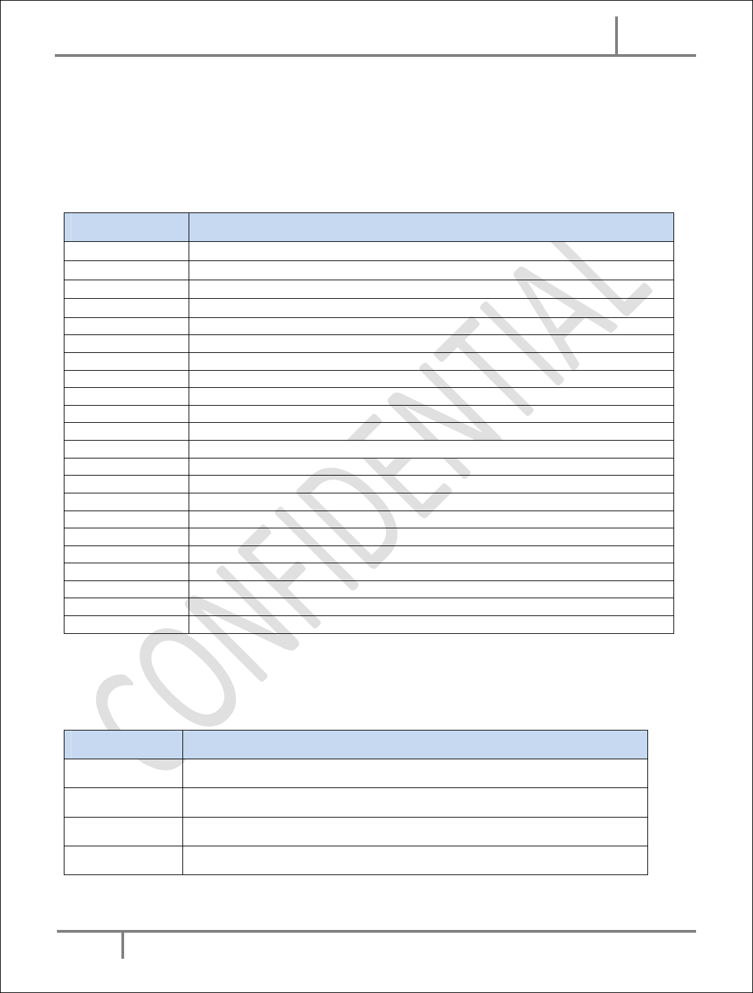
6.1 Pin Detail
Sr. #
Pin Name
Pin Type
Description
1
GND
Ground
Ground Pin must be connected to solid GND plane
2
GND
Ground
Ground Pin must be connected to solid GND plane
3
GND
Ground
Ground Pin must be connected to solid GND plane
4
P0.25
Digital I/O
General purpose I/O pin
5
P0.26
Digital I/O
General purpose I/O pin
6
P0.27
Digital I/O
General purpose I/O pin
7
P0.28
AIN4
Digital I/O
Analog input
General purpose I/O pin
SAADC/COMP/LPCOMP input
8
P0.29
AIN5
Digital I/O
Analog input
General purpose I/O pin
SAADC/COMP/LPCOMP input
9
P0.30
AIN6
Digital I/O
Analog input
General purpose I/O pin
SAADC/COMP/LPCOMP input
10
P0.31
AIN7
Digital I/O
Analog input
General purpose I/O pin
SAADC/COMP/LPCOMP input
11
DEC4
Power
1V3 regulator supply decoupling
Input from DC/DC regulator
Output from 1.3 V LDO*
1
12
DCC
Power
DC/DC regulator output pin*
2
13
VCC
Power
Power Supply pin*
3
14
GND
Ground
Ground Pin must be connected to solid GND plane
15
P0.00
XL1
Digital I/O
Analog input
General purpose I/O pin
Connection for 32.768 kHz crystal (LFXO)
16
P0.01
XL2
Digital I/O
Analog input
General purpose I/O pin
Connection for 32.768 kHz crystal (LFXO)
17
P0.02
AIN0
Digital I/O
Analog input
General purpose I/O pin
SAADC/COMP/LPCOMP input
18
P0.03
AIN1
Digital I/O
Analog input
General purpose I/O pin
SAADC/COMP/LPCOMP input
19
P0.04
AIN2
Digital I/O
Analog input
General purpose I/O pin
SAADC/COMP/LPCOMP input

Bluetooth Module BTIN0011 user manual
2017
7
20
P0.05
AIN3
Digital I/O
Analog input
General purpose I/O pin
SAADC/COMP/LPCOMP input
21
P0.06
Digital I/O
General purpose I/O pin
22
P0.07
Digital I/O
General purpose I/O pin
23
P0.08
Digital I/O
General purpose I/O pin
24
P0.09
NFC1
Digital I/O
NFC input
General purpose I/O pin
NFC antenna connection
25
P0.10
NFC2
Digital I/O
NFC input
General purpose I/O pin
NFC antenna connection
26
GND
Ground
Ground Pin must be connected to solid GND plane
27
P0.11
Digital I/O
General purpose I/O pin
28
P0.12
Digital I/O
General purpose I/O pin
29
P0.13
Digital I/O
General purpose I/O pin
30
P0.14
TRACEDATA[3]
Digital I/O
General purpose I/O pin
Trace port output
31
P0.15
TRACEDATA[2]
Digital I/O
General purpose I/O pin
Trace port output
32
P0.16
TRACEDATA[1]
Digital I/O
General purpose I/O pin
Trace port output
33
P0.17
Digital I/O
General purpose I/O pin
34
P0.18
TRACEDATA[0]
SWO
Digital I/O
General purpose I/O pin
Trace port output
Single Wire output
35
P0.19
Digital I/O
General purpose I/O pin
36
P0.20
TRACECLK
Digital I/O
General purpose I/O pin
Trace port clock output
37
P0.21
RESET
Digital I/O
General purpose I/O pin
Configurable as pin reset
38
SWDCLK
Digital input
Serial Wire Debug clock input for debug
and programming
39
SWDIO
Digital I/O
Serial Wire Debug I/O for debug and
programming
40
P0.22
Digital I/O
General purpose I/O pin
41
P0.23
Digital I/O
General purpose I/O pin
42
P0.24
Digital I/O
General purpose I/O pin
43
GND
Ground
Ground Pin must be connected to solid GND plane
Note:
1) Use 1 F capacitor to ground at DEC4 pin number 11.
2) Use 0.1 F capacitor to ground at VCC pin number 13.
3) Use 15 H, 10 H at DCC pin number 12 for DC/DC Regulator setup.

Bluetooth Module BTIN0011 user manual
2017
8
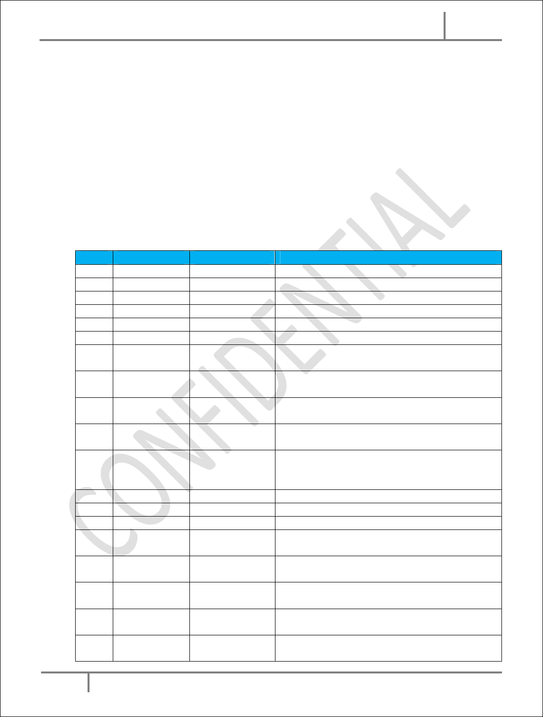
7 Electrical Specification
Absolute Maximum Ratings
(1)
:
Over operating free-air temperature range (unless otherwise noted)
Min
Max
Unit
Supply Voltage
All supply pin must have same
voltage
-0.3
3.9
V
Voltage on any
digital pin
Vi/o, VDD <= 3.6 V
Vi/o, VDD > 3.6 V
-0.3
-0.3
Vdd+0.3
3.9 V
V
Storage Temp
Range
-40
+125
⁰C
NFC antenna pin
current, I
NFC1/2
80
mA
Radio, RF Input
level
10
dBm
MSL
Moisture Sensitivity Level
2
ESD
(2)
All pins, according to human-body
model, JEDEC STD 22, 1 kV method
A114
4
kV
According to charged-device model,
JEDEC STD 22, method C101
750
V
Flash memory
Endurance
10000
Write/erase
cycles
Flash memory
retention
10
years
at
40
℃
(1) Stresses beyond those listed under Absolute Maximum Ratings may cause permanent
damage to the device. These are stress ratings only and functional operation of the device at
these or any other conditions beyond those indicated under Recommended Operating
Conditions are not implied. Exposure to absolute-maximum-rated conditions for extended
periods may affect device reliability.
(2) CAUTION: ESD sensitive device. Precautions should be used when handling the device in
order to prevent permanent damage.
Bluetooth Module BTIN0011 user manual
2017
9
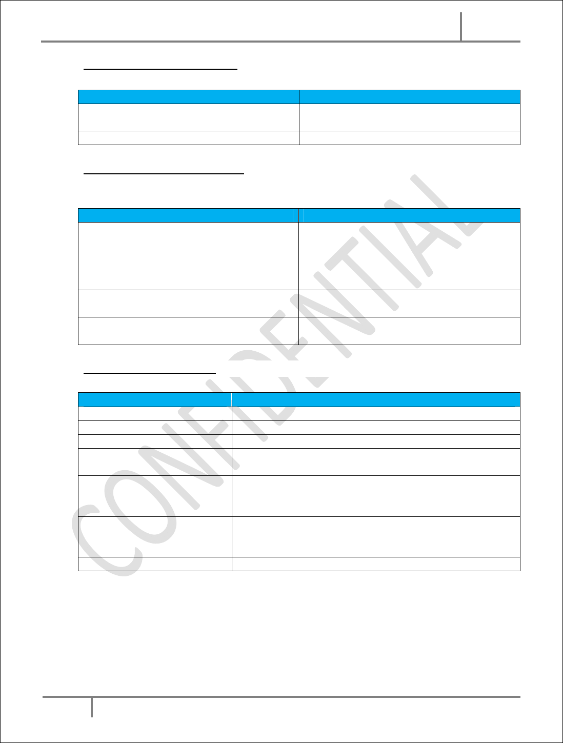
Operating Condition summary:
Items
Specification
Supply Voltage (VDD), independent of DCDC
enable
1.7 V min to Max. +3.6V
Ambient Temperature range
-40 ⁰C to 85 ⁰C
Current Consumption Summary:
Measurement done at TA = 25 ⁰C, VDD = 3V
Items
Specification
System current consumption
0.4μA – No RAM retention,
1.2μA – All peripherals in IDLE mode,
1.6μA – All peripherals in IDLE mode and
32KHz XO and RTC running,
40nA per 4KB - RAM retention
Radio RX @ 1 Mb/s Bluetooth Low Energy
mode, Clock = HFXO
6.5 mA
0 dBm TX @ 1 Mb/s Bluetooth Low Energy
mode, Clock = HFXO
7.1 mA
RF Specification Summary:
Items
Specification
Frequency band
2.402 – 2.480 GHz
Data rate and Modulation
1 Mbps, GFSK
Number of Channel
40: 37 data /3 advertising
Sensitivity
-96dBm Bluetooth, -92.5dBm at 1Mbs ANT,
-89dBm at 2Mbs, -30dBm whisper mode
Radio current
consumption LDO
at 1.8V
15.2mA – TX at +4dBM output power,
10mA – TX at 0dBm output power,
10.4mA – RX at 1Mbs
Radio current
consumption DC-DC
at 3V
7.7mA – TX at +4dBm output power,
5.5mA – TX at 0dBm output power,
5.5mA – RX at 1Mbs
Output power
-20 to +4 dBm
Bluetooth Module BTIN0011 user manual
2017
10
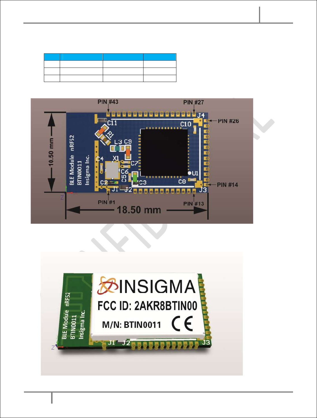
8 Mechanical Specification
No.
Item
Dimension
Tolerance
1.
Length
18.5 mm
+/- 0.20
2.
Width
10.5 mm
+/- 0.20
3.
Height
2.7 mm
+/- 0.20
Note: All Dimensions are in mm.

Bluetooth Module BTIN0011 user manual
2017
11
9 Regulatory Statement
9.1 FCC Statement:
This equipment has been tested and found to comply with the limits for a Class B digital device,
pursuant to Part 15 of the FCC Rules. These limits are designed to provide reasonable
protection against harmful interference in a residential installation. This equipment generates
uses and can radiate radio frequency energy and, if not installed and used in accordance with
the instructions, may cause harmful interference to radio communications. However, there is no
guarantee that interference will not occur in a particular installation. If this equipment does
cause harmful interference to radio or television reception, which can be determined by turning
the equipment off and on, the user is encouraged to try to correct the interference by one or
more of the following measures:
Reorient or relocate the receiving antenna.
Increase the separation between the equipment and receiver.
Connect the equipment into an outlet on a circuit different from that to which the receiver
is connected.
Consult the dealer or an experienced radio/TV technician for help.
The module in this product is labeled with its own FCC ID No. The FCC ID and is not visible
when the module is installed inside another device. Therefore, the outside of the device into
which the module is installed must also display a label referring to the module. The final end
device must be labeled in a visible area with the following
“Contains FCC ID: 2AKR8BTIN00”
9.2 FCC Caution:
The user is cautioned that changes or modifications not expressly approved by the Insigma
responsible for compliance could void the user's authority to operate the equipment.
This device complies with Part 15 of the FCC Rules. Operation is subject to the following two
conditions:
(1) This device may not cause harmful interference, and
(2) This device must accept any interference received, including interference that may cause undesired
operation
9.3 FCC Radiation Exposure Statement:
This equipment complies with FCC radiation exposure limits set forth for an uncontrolled
environment.
This transmitter must not be co-located or operating in conjunction with any other antenna or
transmitter.
Bluetooth Module BTIN0011 user manual
2017
12
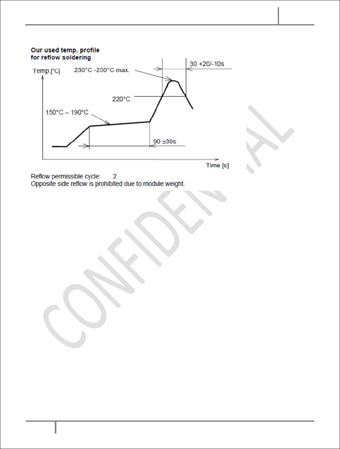
10 Soldering Temperature Profile
Bluetooth Module BTIN0011 user manual
2017
13
11 Document History
Version
Date completed Written by Reviewed by Approved by
1.0 08/24/2016 Hiren Jayani
Initial version
1.1 12/15/2016 Manish Patel
Change in Mechanical Specification
1.2 01/23/2017 Ravi Chaudhari
Updated FCC statement.