Intel 324632 003 Intel® 82575EB Gigabit Ethernet Controller Software Developer’s Manual And EEPROM Guide User To The 1225128d 56bb 4f2f Aa25 0479ccaef100
User Manual: Intel 324632-003 to the manual
Open the PDF directly: View PDF ![]() .
.
Page Count: 456 [warning: Documents this large are best viewed by clicking the View PDF Link!]
- Intel® 82575EB Gigabit Ethernet Controller Software Developer’s Manual and EEPROM Guide
- 1.0 Introduction
- 2.0 Architectural Overview
- 3.0 General Initialization and Reset Operation
- 4.0 EEPROM and Flash Interface
- 4.1 EEPROM Device
- 4.2 Flash Interface Operation
- 4.3 Shared EEPROM
- 4.4 Shared FLASH
- 4.5 EEPROM Map
- 4.5.1 Hardware Accessed Words
- 4.5.1.1 Ethernet Address (Words 00h – 02h)
- 4.5.1.2 Initialization Control 1 (Word 0Ah)
- 4.5.1.3 Subsystem ID (Word 0Bh)
- 4.5.1.4 Subsystem Vendor ID (Word 0Ch)
- 4.5.1.5 Device ID (Word 0Dh, 11h)
- 4.5.1.6 Dummy Device ID (Word 1Dh)
- 4.5.1.7 Initialization Control 2 (Word 0Fh)
- 4.5.1.8 Software Defined Pins Control (Word 10h)
- 4.5.1.9 EEPROM Sizing & Protected Fields (Word 12h)
- 4.5.1.10 Initialization Control 3 (Word 14h, 24h)
- 4.5.1.11 NC-SI and PCIe* Completion Timeout Configuration (Word 15h)
- 4.5.1.12 MSI-X Configuration (Word 16h)
- 4.5.1.13 PLL/Lane/PHY Initialization Pointer (Word 17h)
- 4.5.1.14 PCIe* Initialization Configuration 1 (Word 18h)
- 4.5.1.15 PCIe* Initialization Configuration 2 (Word 19h)
- 4.5.1.16 Software Defined Pins Control (Word 20h)
- 4.5.1.17 PCIe* Initialization Configuration 3 (Word 1Ah)
- 4.5.1.18 PCIe* Control (Word 1Bh)
- 4.5.1.19 LED 1, 3 Configuration Defaults (Word 1Ch)
- 4.5.1.20 Device Revision ID (Word 1Eh)
- 4.5.1.21 LED 0, 2 Configuration Defaults (Word 1Fh)
- 4.5.1.22 Functions Control (Word 21h)
- 4.5.1.23 LAN Power Consumption (Word 22h)
- 4.5.1.24 Management Hardware Configuration Control (Word 23h)
- 4.5.1.25 End of RO Area (Word 2Ch
- 4.5.1.26 Start of RO Area (Word 2Dh)
- 4.5.1.27 Watchdog Configuration (Word 2Eh)
- 4.5.1.28 VPD Pointer (Word 2Fh)
- 4.5.1.29 PXE Words (Words 30h:3Eh)
- 4.5.1.29.1 Main Setup Options PCI Function 0 (Word 30h)
- 4.5.1.29.2 Configuration Customization Options PCI Function 0 (Word 31h)
- 4.5.1.29.3 PXE Version (Word 32h)
- 4.5.1.29.4 IBA Capabilities (Word 33h)
- 4.5.1.29.5 Setup Options PCI Function 1 (Word 34h)
- 4.5.1.29.6 Configuration Customization Options PCI Function 1 (Word 35h)
- 4.5.1.29.7 iSCSI Option ROM Version (Word 36h)
- 4.5.1.29.8 Alternate MAC Address Pointer (Word 37h)
- 4.5.1.29.9 Setup Options PCI Function 2 (Word 38h)
- 4.5.1.29.10 Configuration Customization Options PCI Function 2 (Word 39h)
- 4.5.1.29.11 Setup Options PCI Function 3 (Word 3Ah)
- 4.5.1.29.12 Configuration Customization Options PCI Function 3 (Word 3Bh)
- 4.5.1.29.13 iSCSI Boot Configuration Offset (Word 3Dh)
- 4.5.1.29.14 Checksum Word (Word 3Fh)
- 4.5.1 Hardware Accessed Words
- 4.6 Manageability Control Sections
- 4.6.1 Sideband Configuration Structure
- 4.6.1.1 Section Header - (0ffset 0h)
- 4.6.1.2 SMBus Max Fragment Size - (0ffset 01h)
- 4.6.1.3 SMBus Notification Timeout and Flags - (0ffset 02h)
- 4.6.1.4 SMBus Slave Addresses - (0ffset 03h)
- 4.6.1.5 SMBus Fail-Over Register (Low Word) - (0ffset 04h)
- 4.6.1.6 SMBus Fail-Over Register (High Word) - (0ffset 05h)
- 4.6.1.7 NC-SI Configuration (0ffset 06h)
- 4.6.2 Flex TCO Filter Configuration Structure
- 4.6.3 NC-SI Microcode Download Structure
- 4.6.4 NC-SI Configuration Structure
- 4.6.4.1 Section Header - (0ffset 0h)
- 4.6.4.2 Rx Mode Control1 (RR_CTRL[15:0]) (Offset 01h)
- 4.6.4.3 Rx Mode Control2 (RR_CTRL[31:16]) (Offset 02h)
- 4.6.4.4 Tx Mode Control1 (RT_CTRL[15:0]) (Offset 03h)
- 4.6.4.5 Tx Mode Control2 (RT_CTRL[31:16]) (Offset 04h)
- 4.6.4.6 MAC Tx Control Reg1 (TxCntrlReg1 (15:0]) (Offset 05h)
- 4.6.4.7 MAC Tx Control Reg2 (TxCntrlReg1 (31:16]) (Offset 06h)
- 4.6.5 Common Firmware Pointer
- 4.6.6 Pass Through Pointers
- 4.6.7 PT LAN Configuration Structure
- 4.6.7.1 Section Header (Offset 0h)
- 4.6.7.2 LAN0 IPv4 Address 0 LSB, MIPAF0 (Offset 01h)
- 4.6.7.3 LAN0 IPv4 Address 0 LSB, MIPAF0 (Offset 02h)
- 4.6.7.4 LAN0 IPv4 Address 1; MIPAF1 (Offset 03h:04h)
- 4.6.7.5 LAN0 IPv4 Address 2; MIPAF2 (Offset 05h:06h)
- 4.6.7.6 LAN0 IPv4 Address 3; MIPAF3 (Offset 07h:08h)
- 4.6.7.7 LAN0 MAC Address 0 LSB, MMAL0 (Offset 09h)
- 4.6.7.8 LAN0 MAC Address 0 LSB, MMAL0 (Offset 0Ah)
- 4.6.7.9 LAN0 MAC Address 0 MSB, MMAH0 (Offset 0Bh)
- 4.6.7.10 LAN0 MAC Address 1; MMAL/H1 (Offset 0Ch:0Eh)
- 4.6.7.11 LAN0 MAC Address 2; MMAL/H2 (Offset 0Fh:11h)
- 4.6.7.12 LAN0 MAC Address 3; MMAL/H3 (Offset 12h:14h)
- 4.6.7.13 LAN0 UDP Flex Filter Ports 0:15; MFUTP Registers (Offset 15h:24h)
- 4.6.7.14 LAN0 VLAN Filter 0:7; MAVTV Registers (Offset 25h:2Ch)
- 4.6.7.15 LAN0 Manageability Filters Valid; MFVAL LSB (Offset 2Dh)
- 4.6.7.16 LAN0 Manageability Filters Valid; MFVAL MSB (Offset 2Eh)
- 4.6.7.17 LAN0 MAC Value MSB (Offset 2Fh)
- 4.6.7.18 LAN0 MANC Value LSB (Offset 30h)
- 4.6.7.19 LAN0 Receive Enable 1(Offset 31h)
- 4.6.7.20 LAN0 Receive Enable 2 (Offset 32h)
- 4.6.7.21 LAN0 MANC2H Value LSB (Offset 33h)
- 4.6.7.22 LAN0 MANC2H Value MSB (Offset 34h)
- 4.6.7.23 Manageability Decision Filters; MDEF0,1 (Offset 35h)
- 4.6.7.24 Manageability Decision Filters; MDEF0, 2 (Offset 36h)
- 4.6.7.25 Manageability Decision Filters; MDEF1:6, 1:2 (Offset 37h:42h)
- 4.6.7.26 ARP Response IPv4 Address 0 LSB (Offset 43h)
- 4.6.7.27 ARP Response IPv4 Address 0 MSB (Offset 44h)
- 4.6.7.28 LAN0 IPv6 Address 0 LSB; MIPAF (Offset 45h)
- 4.6.7.29 LAN0 IPv6 Address 0 MSB; MIPAF (Offset 46h)
- 4.6.7.30 LAN0 IPv6 Address 0 LSB; MIPAF (Offset 47h)
- 4.6.7.31 LAN0 IPv6 Address 0 MSB; MIPAF (Offset 48h)
- 4.6.7.32 LAN0 IPv6 Address 0 LSB; MIPAF (Offset 49h)
- 4.6.7.33 LAN0 IPv6 Address 0 MSB; MIPAF (Offset 4Ah)
- 4.6.7.34 LAN0 IPv6 Address 0 LSB; MIPAF (Offset 4B)
- 4.6.7.35 LAN0 IPv6 Address 0 MSB; MIPAF (Offset 4Ch)
- 4.6.7.36 LAN0 IPv6 Address 1; MIPAF (Offset 4Dh)
- 4.6.7.37 LAN0 IPv6 Address 2; MIPAF (Offset 55h:5Ch)
- 4.6.1 Sideband Configuration Structure
- 4.7 Software Owned EEPROM Words
- 5.0 Receive and Transmit Description
- 5.1 82575 Data Flows
- 5.2 Receive Data Flow
- 5.3 Receive Functionality
- 5.3.1 Packet Address Filtering
- 5.3.2 Receive Data Storage
- 5.3.3 Legacy Receive Descriptor Format
- 5.3.4 Advanced Receive Descriptors
- 5.3.4.1 Packet Buffer Address
- 5.3.4.2 Header Buffer Address
- 5.3.4.3 Packet Type
- 5.3.4.4 RSS Type
- 5.3.4.5 Split Header
- 5.3.4.6 Packet Checksum
- 5.3.4.7 RSS Hash Value
- 5.3.4.8 Extended Status
- 5.3.4.9 Extended Errors
- 5.3.4.10 Packet Buffer (Number of Bytes Exists in the Host Packet Buffer)
- 5.3.4.11 VLAN Tag Field
- 5.3.5 Receive UDP Fragmentation Checksum
- 5.3.6 Receive Descriptor Fetching
- 5.3.7 Receive Descriptor Write-Back
- 5.3.8 Receive Descriptor Ring Structure
- 5.4 Multiple Receive Queues
- 5.5 Header Splitting and Replication
- 5.6 Packet Transmission
- 5.7 Transmit Descriptor Ring Structure
- 5.8 TCP Segmentation
- 5.9 IP/TCP/UDP Transmit Checksum Offloading
- 5.10 IP/TCP/UDP Transmit Checksum Offloading in Non-Segmentation Mode
- 5.11 Multiple Transmit Queues
- 5.12 Tx Completions Head Write-Back
- 5.13 Interrupts
- 5.13.1 Interrupt Cause Register (ICR)
- 5.13.2 Interrupt Cause Set Register (ICS)
- 5.13.3 Interrupt Mask Set/Read Register (IMS)
- 5.13.4 Interrupt Mask Clear Register (IMC)
- 5.13.5 Interrupt Acknowledge Auto-mask register (IAM)
- 5.13.6 Extended Interrupt Cause Registers (EICR)
- 5.13.7 Extended Interrupt Cause Set Register (EICS)
- 5.13.8 Extended Interrupt Mask Set and Read Register (EIMS)/Extended Interrupt Mask Clear Register (EIMC)
- 5.13.9 Extended Interrupt Auto Clear Enable Register (EIAC)
- 5.13.10 Extended Interrupt Auto Mask Enable Register (EIAM)
- 5.13.11 Interrupt Modes Setting Bits
- 5.14 Interrupt Moderation
- 5.15 Clearing Interrupt Causes
- 5.16 Dynamic Interrupt Moderation
- 5.17 Memory Error Correction and Detection
- 6.0 PCIe* Local Bus Interface
- 6.1 General Functionality
- 6.2 Flow Control
- 6.3 Host Interface
- 6.4 Error Events and Error Reporting
- 6.5 Link Layer
- 6.6 Physical Layer
- 7.0 Power Management
- 7.1 Power States
- 7.2 Auxiliary Power
- 7.3 Form Factor Power Limits
- 7.4 Power Management Interconnects
- 7.5 Wake Up
- 8.0 DCA
- 9.0 Ethernet Interface
- 9.1 Internal MAC/PHY 10/100/1000Base-T Interface
- 9.2 Duplex Operation for Copper PHY Operation
- 9.3 Auto-Negotiation and Link Setup
- 9.4 Loopback Support
- 10.0 802.1q VLAN Support
- 11.0 PHY Functionality and Features
- 11.1 Auto MDIO Register Initialization
- 11.2 Determining Link State
- 11.3 Link Criteria
- 11.4 Link Enhancements
- 11.5 Management Data Interface
- 11.6 Low Power Operation
- 11.7 Power Down via the PHY Register
- 11.8 1000 Mb/s Operation
- 11.9 100 Mb/s Operation
- 11.10 10 Mb/s Operation
- 12.0 Configurable LED Outputs
- 13.0 Dual Port Characteristics
- 14.0 Register Descriptions
- 14.1 Register Conventions
- 14.2 Register Summary
- 14.3 Main Register Descriptions
- 14.3.1 Device Control Register - CTRL (00000h; R/W)
- 14.3.2 Device Status Register - STATUS (00008h; R)
- 14.3.3 EEPROM/Flash Control Register - EEC (00010h; R/W)
- 14.3.4 EEPROM Read Register - EERD (00014h; RW)
- 14.3.5 Extended Device Control Register - CTRL_EXT (00018h, R/W)
- 14.3.6 Flash Access - FLA (0001Ch; R/W)
- 14.3.7 MDI Control Register - MDIC (00020h; R/W)
- 14.3.8 PHY Registers
- 14.3.8.1 PHY Control Register - PCTRL (00d; R/W)
- 14.3.8.2 PHY Status Register - PSTATUS (01d; R)
- 14.3.8.3 PHY Identifier Register 1 (LSB) - PHY ID 1 (02d; R)
- 14.3.8.4 PHY Identifier Register 2 (MSB) - PHY ID 2 (03d; R)
- 14.3.8.5 Auto-Negotiation Advertisement Register - ANA (04d; R/W)
- 14.3.8.6 Auto-Negotiation Base Page Ability Register - (05d; R)
- 14.3.8.7 Auto-Negotiation Expansion Register - ANE (06d; R)
- 14.3.8.8 Auto-Negotiation Next Page Transmit Register - NPT (07d; R/W)
- 14.3.8.9 Auto-Negotiation Next Page Ability Register - LPN (08d; R)
- 14.3.8.10 1000BASE-T/100BASE-T2 Control Register - GCON (09d; R/W)
- 14.3.8.11 1000BASE-T/100BASE-T2 Status Register - GSTATUS (10d; R)
- 14.3.8.12 Extended Status Register - ESTATUS (15d; R)
- 14.3.8.13 Port Configuration Register - PCONF (16d; R/W)
- 14.3.8.14 Port Status 1 Register - PSTAT (17d; RO)
- 14.3.8.15 Port Control Register - PCONT (18d; R/W)
- 14.3.8.16 Link Health Register - LINK (19d; RO)
- 14.3.8.17 1000Base-T FIFO Register - PFIFO (20d; R/W)
- 14.3.8.18 Channel Quality Register - CHAN (21d; RO)
- 14.3.8.19 PHY Power Management - (25d; R/W)
- 14.3.8.20 Special Gigabit Disable Register - (26d; R/W)
- 14.3.8.21 Misc Cntrl Register 1 - (27d; R/W)
- 14.3.8.22 Misc Cntrl Register 2 - (28d; RO)
- 14.3.8.23 Page Select Core Register - (31d; WO)
- 14.3.9 SERDES ANA - SERDESCTL (00024h; R/W)
- 14.3.10 Copper/Fiber Switch Control - CONNSW (00034h; R/W)
- 14.3.11 VLAN Ether Type - VET (00038h; R/W)
- 14.3.12 Fuse Register - UFUSE (5B78h; RO)
- 14.3.13 Flow Control Address Low - FCAL (00028h; R/ W)
- 14.3.14 Flow Control Address High - FCAH (0002Ch; R/ W)
- 14.3.15 Flow Control Type - FCT (00030h; R/W)
- 14.3.16 Flow Control Transmit Timer Value - FCTTV (00170h; R/W)
- 14.3.17 LED Control - LEDCTL (00E00h; RW)
- 14.3.18 Packet Buffer Allocation - PBA (01000h; R/W)
- 14.3.19 Packet Buffer Size - PBS (01008h; R/W)
- 14.3.20 SFP 12C Command - I2CCMD (01028h; R/W)
- 14.3.21 SFP 12C Parameters - I2CPARAMS (0102Ch; R/ W)
- 14.3.22 Flash Opcode - FLASHOP (0103Ch; R/W)
- 14.3.23 EEPROM Diagnostic - EEDIAG (01038h; RO)
- 14.3.24 Manageability EEPROM Control Register - EEMNGCTL (01010h; RO)
- 14.3.25 Manageability EEPROM Read/Write Data - EEMNGDATA (1014h; RO)
- 14.3.26 Manageability Flash Control Register - FLMNGCTL (1018h; R/W)
- 14.3.27 Manageability Flash Read Data - FLMNGDATA (101Ch; R/W)
- 14.3.28 Manageability Flash Read Counter - FLMNGCNT (1020h; R/W)
- 14.3.29 EEPROM Auto Read Bus Control - EEARBC (01024h; R/W)
- 14.3.30 Watchdog Setup - WDSTP (01040h; R/W)
- 14.3.31 Watchdog SW Device Status - WDSWSTS (01044h; R/W)
- 14.3.32 Free Running Timer - FRTIMER (01048h; RWS)
- 14.3.33 TCP Timer - TCPTIMER (0104Ch; R/W)
- 14.3.34 Interrupt Cause Read Register - ICR (000C0H; R)
- 14.3.35 Interrupt Cause Set Register - ICS (000C8h; WO)
- 14.3.36 Interrupt Mask Set/Read Register - IMS (000D0h; R/W)
- 14.3.37 Interrupt Mask Clear Register - IMC (000D8h; W)
- 14.3.38 Interrupt Acknowledge Auto Mask Register - IAM (000E0h; R/W)
- 14.3.39 Extended Interrupt Cause - EICR (01580h; RC/ W1C)
- 14.3.40 Extended Interrupt Cause Set - EICS (01520h; WO)
- 14.3.41 Extended Interrupt Mask Set/Read - EIMS (01524h; RWS)
- 14.3.42 Extended Interrupt Mask Clear - EIMC (01528h; WO)
- 14.3.43 Extended Interrupt Auto Clear - EIAC (0152Ch; R/W)
- 14.3.44 Extended Interrupt Auto Mask Enable - EIAM (01530h; R/W)
- 14.3.45 Interrupt Throttle - EITR (01680h + 4*n [n = 0..9]; R/W)
- 14.3.46 Immediate Interrupt Rx - IMIR (05A80h + 4*n [n = 0..7]; R/W)
- 14.3.47 Immediate Interrupt Rx Extended - IMIREXT (05AA0h + 4*n [n = 0..7]; R/W)
- 14.3.48 Immediate Interrupt Rx VLAN Priority - IMIRVP (05AC0h; R/W)
- 14.3.49 MSI-X Allocation - MSIXBM (01600h + 4*n [n = 0..9]; R/W)
- 14.3.50 Receive Control Register - RCTL (00100h; R/W)
- 14.3.51 Split and Replication Receive Control - SRRCTL (0280Ch + 100*n [n=0..3]; R/W)
- 14.3.52 Packet Split Receive Type - PSRTYPE (05480h + 4*n [n=0..3]; R/W)
- 14.3.53 Flow Control Receive Threshold Low - FCRTL (02160h; R/W)
- 14.3.54 Flow Control Receive Threshold High - FCRTH (02168h; R/W)
- 14.3.55 Flow Control Refresh Threshold Value - FCRTV (02460h; R/W)
- 14.3.56 Receive Descriptor Base Address High - RDBAH (02804h + 100*n [n=0..3]; R/W)
- 14.3.57 Receive Descriptor Length - RDLEN (02808h + 100*n [n=0..3]; R/W)
- 14.3.58 Receive Descriptor Head - RDH (02810h + 100*n [n=0..3]; R/W)
- 14.3.59 Receive Descriptor Tail - RDT (02818h + 100*n [n=0..3]; R/W)
- 14.3.60 Receive Descriptor Control - RXDCTL (02828h + 100*n [n=0..3]; R/W)
- 14.3.61 Receive Checksum Control - RXCSUM (05000h; R/W)
- 14.3.62 Receive Long Packet Maximum Length - RLPML (05004; R/W)
- 14.3.63 Receive Filter Control Register - RFCTL (05008h; R/W)
- 14.3.64 Transmit Control Register - TCTL (00400h; R/ W)
- 14.3.65 Transmit Control Extended - TCTL_EXT (00404;R/W)
- 14.3.66 Transmit IPG Register - TIPG (00410;R/W)
- 14.3.67 DMA Tx Control - DTXCTL (03590h; R/W)
- 14.3.68 Transmit Descriptor Base Address Low - TDBAL (03800h + 100*n [n=0..3]; R/W)
- 14.3.69 Transmit Descriptor Base Address High - TDBAH (03804h + 100*n [n=0..3]; R/W)
- 14.3.70 Transmit Descriptor Length - TDLEN (03808h + 100*n [n=0..3]; R/W)
- 14.3.71 Transmit Descriptor Head - TDH (03810h + 100*n [n=0..3]; R/W)
- 14.3.72 Transmit Descriptor Tail - TDT (03818h + 100*n [n=0..3]; R/W)
- 14.3.73 Transmit Descriptor Control - TXDCTL (03828h + 100*n [n=0..3]; R/W)
- 14.3.74 Tx Descriptor Completion Write-Back Address Low - TDWBAL (03838h + 100*n [n=0..3]; R/ W)
- 14.3.75 Tx Descriptor Completion Write-Back Address High - TDWBAH (0383Ch + 100*n [n=0..3]; R/ W)
- 14.3.76 PCS Configuration 0 - PCS_CFG (04200h; R/W)
- 14.3.77 PCS Link Control - PCS_LCTL (04208h; R/W)
- 14.3.78 PCS Link Status - PCS_LSTS (0420Ch; R/W)
- 14.3.79 AN Advertisement - PCS_ANADV (04218h; R/ W)
- 14.3.80 Link Partner Ability - PCS_LPAB (0421Ch; RO)
- 14.3.81 Next Page Transmit - PCS_NPTX (04220h; RO)
- 14.3.82 Link Partner Ability Next Page - PCS_LPABNP (04224h; RO)
- 14.4 DCA Registers
- 14.5 Filter Registers
- 14.5.1 Multicast Table Array - MTA (05200h + 4*n [n..127]; R/W)
- 14.5.2 Receive Address Low - RAL (05400h + 8*n [n=0..15]; R/W)
- 14.5.3 Receive Address High - RAH (05404h + 8*n [n=0..15]; R/W)
- 14.5.4 VLAN Filter Table Array - VFTA (05600h + 4*n [n=0..127]; R/W)
- 14.5.5 Multiple Receive Queues Command Register - MRQC (05818h; R/W)
- 14.5.6 Redirection Table - RETA (05C00h + 4*n [n=0..31]; R/W)
- 14.5.7 RSS Random Key Register - RSSRK (05C80h + 4*n [n=0..9]; R/W)
- 14.5.8 VMDq Control - VMD_CTRL (0581Ch; R/W)
- 14.5.9 VLAN Filter Queue Array 0 - VFQA0 (0B100h + 4*n [n=0…127]; R/W)
- 14.5.10 VLAN Filter Queue Array 1 - VFQA1 (0B200h + 4*n [n=0…127]; R/W)
- 14.6 Wakeup Registers
- 14.6.1 Wakeup Control Register - WUC (05800h; R/W)
- 14.6.2 Wakeup Filter Control Register - WUFC (05808h; R/W)
- 14.6.3 Wakeup Status Register - WUS (05810h; R/ W1C)
- 14.6.4 IP Address Valid - IPAV (5838h; R/W)
- 14.6.5 IPv4 Address Table - IP4AT (05840h + 8*n [n=0..3]; R/W)
- 14.6.6 IPv6 Address Table - IP6AT (05880h + 4*n[n=0..3]; R/W)
- 14.6.7 Wakeup Packet Length - WUPL (05900h; RC)
- 14.6.8 Wakeup Packet Memory (128 Bytes) - WUPM (05A00h + 4*n [n=0..31]; RC)
- 14.6.9 Flexible Filter Mask Table - FFMT (09000h + 8*n [n=0..127]; R/W)
- 14.6.10 Flexible Filter Value Table - FFVT (09800h + 8*n [n=0..127]; R/W)
- 14.6.11 Flexible Filter Length Table - FFLT (05F00h + 8*n [n=0..3]; R/W)
- 14.7 Manageability Registers
- 14.7.1 Management VLAN TAG Value - MAVTV (5010h +4*n [n=0..7]; R/W)
- 14.7.2 Management Flex UDP/TCP Ports - MFUTP (5030h + 4*n [n=0..7]; R/W)
- 14.7.3 Management Control Register - MANC (05820h; R/W)
- 14.7.4 Manageability Filters Valid - MFVAL (5824h; R/ W)
- 14.7.5 Management Control to Host Register - MANC2H (5860h; R/W)
- 14.7.6 Manageability Decision Filters- MDEF (5890h + 4*n [n=0..7]; R/W)
- 14.7.7 Manageability IP Address Filter - MIPAF (0x58B0-0x58EC; RW)
- 14.7.8 Manageability MAC Address Low - MMAL (5910h + 8*n[n=0..3]; RW)
- 14.7.9 Manageability MAC Address High - MMAH (0x5914 + 8*n[n=0..3]; RW)
- 14.7.10 Flexible TCO Filter Table Registers - FTFT (09400h-097FCh; RW)
- 14.7.11 Legacy Sensor Polling Mask 1...8 Register (F8h:FFh)
- 14.8 PCIe* Registers
- 14.8.1 PCIe* Control - GCR (05B00h; R)
- 14.8.2 Function Tag - FUNCTAG (05B08h; R/W)
- 14.8.3 PCIe* Statistics Control #1 - GSCL_1 (05B10h; R)
- 14.8.4 PCIe* Statistics Control #2 - GSCL_2 (05B14h; R)
- 14.8.5 PCIe* Statistics Control #3 - GSCL_3 (05B18h; R/W)
- 14.8.6 PCIe* Statistics Control #4 - GSCL_4 (05B1Ch; R/W)
- 14.8.7 PCIe* Counter #0 - GSCN_0 (05B20h; R/W)
- 14.8.8 PCIe* Counter #1 - GSCN_1 (05B24h; R/W)
- 14.8.9 PCIe* Counter #2 - GSCN_2 (05B28h; R/W)
- 14.8.10 PCIe* Counter #3 - GSCN_3 (05B2Ch; R/W)
- 14.8.11 Function Active and Power State to MNG - FACTPS (05B30h; R)
- 14.8.12 SerDes/CCM/PCIe* CSR - GIOANACTL0 (05B34h; R/W)
- 14.8.13 SerDes/CCM/PCIe* CSR - GIOANACTL1 (05B38h; R/W)
- 14.8.14 GIOANACTL2 (05B3Ch; R/W)
- 14.8.15 GIOANACTL3 (05B40h; R/W)
- 14.8.16 SerDes/CCM/PCIe* CSR - GIOANACTLALL (05B44h; R/W)
- 14.8.17 SerDes/CCM/PCIe* CSR - CCMCTL (05B48h; R/ W)
- 14.8.18 SerDes/CCM/PCIe* CSR - SCCTL (05B4Ch; R/ W)
- 14.8.19 Software Semaphore - SWSM (05B50h; R/W)
- 14.8.20 Firmware Semaphore - FWSM (05B58h; R/WS)
- 14.8.21 Software-Firmware Synchronization - SW_FW_SYNC (05B5Ch; R/WS)
- 14.8.22 Mirrored Revision ID - MREVID (05B64h; R/W)
- 14.8.23 MSI-X PBA Clear - PBACL (05B68h; R/W1C)
- 14.8.24 DCA Requester ID Information - DCA_ID (05B70h; R/W)
- 14.8.25 DCA Control - DCA_CTRL (05B74h; R/W)
- 14.9 Statistics Registers
- 14.9.1 CRC Error Count - CRCERRS (04000h; RC)
- 14.9.2 Alignment Error Count - ALGNERRC (04004h; RC)
- 14.9.3 Symbol Error Count - SYMERRS (04008h; RC)
- 14.9.4 RX Error Count - RXERRC (0400Ch; RC)
- 14.9.5 Missed Packets Count - MPC (04010h; RC)
- 14.9.6 Single Collision Count - SCC (04014h; RC)
- 14.9.7 Excessive Collisions Count - ECOL (04018h; RC)
- 14.9.8 Multiple Collision Count - MCC (0401Ch; RC)
- 14.9.9 Late Collisions Count - LATECOL (04020h; RC)
- 14.9.10 Collision Count - COLC (04028h; RC)
- 14.9.11 Defer Count - DC (04030h; RC)
- 14.9.12 Transmit with No CRS - TNCRS (04034h; RC)
- 14.9.13 Receive Length Error Count - RLEC (04040h; RC)
- 14.9.14 XON Received Count - XONRXC (04048h; RC)
- 14.9.15 XON Transmitted Count - XONTXC (0404Ch; RC)
- 14.9.16 XOFF Received Count - XOFFRXC (04050h; RC)
- 14.9.17 XOFF Transmitted Count - XOFFTXC (04054h; RC)
- 14.9.18 FC Received Unsupported Count - FCRUC (04058h; RC)
- 14.9.19 Packets Received (64 Bytes) Count - PRC64 (0405Ch; RC)
- 14.9.20 Packets Received (65-127 Bytes) Count - PRC127 (04060h; RC)
- 14.9.21 Packets Received (128-255 Bytes) Count - PRC255 (04064h; RC)
- 14.9.22 Packets Received (256-511 Bytes) Count - PRC511 (04068h; RC)
- 14.9.23 Packets Received (512-1023 Bytes) Count - PRC1023 (0406Ch; RC)
- 14.9.24 Packets Received (1024 to Max Bytes) Count - PRC1522 (04070h; RC)
- 14.9.25 Good Packets Received Count - GPRC (04074h; RC)
- 14.9.26 Broadcast Packets Received Count - BPRC (04078h; RC)
- 14.9.27 Multicast Packets Received Count - MPRC (0407Ch; RC)
- 14.9.28 Good Packets Transmitted Count - GPTC (04080h; RC)
- 14.9.29 Good Octets Received Count - GORCL (04088h; RC)/GORCH (0408Ch; RC)
- 14.9.30 Good Octets Transmitted Count - GOTCL (04090h; RC)/ GOTCH (04094; RC)
- 14.9.31 Receive No Buffers Count - RNBC (040A0h; RC)
- 14.9.32 Receive Undersize Count - RUC (040A4h; RC)
- 14.9.33 Receive Fragment Count - RFC (040A8h; RC)
- 14.9.34 Receive Oversize Count - ROC (040ACh; RC)
- 14.9.35 Receive Jabber Count - RJC (040B0h; R)
- 14.9.36 Management Packets Received Count - MNGPRC (040B4h; RC)
- 14.9.37 Management Packets Dropped Count - MPDC (040B8h; RC)
- 14.9.38 Management Packets Transmitted Count - MNGPTC (040BCh; RC)
- 14.9.39 Total Octets Received - TORL (040C0h; RC) / TORH (040C4h; RC)
- 14.9.40 Total Octets Transmitted - TOTL (040C8h; RC / TOTH (040CCh; RC)
- 14.9.41 Total Packets Received - TPR (040D0h; RC)
- 14.9.42 Total Packets Transmitted - TPT (040D4h; RC)
- 14.9.43 Packets Transmitted (64 Bytes) Count - PTC64 (040D8h; RC)
- 14.9.44 Packets Transmitted (65-127 Bytes) Count - PTC127 (040DCh; RC)
- 14.9.45 Packets Transmitted (128-255 Bytes) Count - PTC255 (040E0h; RC)
- 14.9.46 Packets Transmitted (256-511 Bytes) Count - PTC511 (040E4h; RC)
- 14.9.47 Packets Transmitted (512-1023 Bytes) Count - PTC1023 (040E8h; RC)
- 14.9.48 Packets Transmitted (1024 Bytes or Greater) Count - PTC1522 (040ECh; RC)
- 14.9.49 Multicast Packets Transmitted Count - MPTC (040F0h; RC)
- 14.9.50 Broadcast Packets Transmitted Count - BPTC (040F4h; RC)
- 14.9.51 TCP Segmentation Context Transmitted Count - TSCTC (040F8h; RC)
- 14.9.52 Interrupt Assertion Count - IAC (04100h; RC)
- 14.9.53 Rx Packets to Host Count - RPTHC (04104h; RC)
- 14.9.54 Transmit Queue Empty Count - TXQEC (04118h; RC)
- 14.9.55 Receive Descriptor Minimum Threshold Count - RXDMTC (04120h; RC)
- 14.9.56 Interrupt Cause Receiver Overrun Count - ICRXOC (04124h; RC)
- 14.9.57 SerDes/SGMII Code Violation Packet Count - SCVPC (04228h; R/WS)
- 14.10 Diagnostics Registers
- 14.10.1 Receive Data FIFO Head Register - RDFH (02410h; RO)
- 14.10.2 Receive Data FIFO Tail Register - RDFT (02418h; RO)
- 14.10.3 Receive Data FIFO Head Saved Register - RDFHS (02420h; RO)
- 14.10.4 Receive Data FIFO Tail Saved Register - RDFTS (02428h; RO)
- 14.10.5 Receive Data FIFO Packet Count - RDFPCQ (02430h + 4 *n [n=0..3]; RO)
- 14.10.6 PB Descriptor Read Pointers - PBDESCRP (02454h; RO)
- 14.10.7 Packet Buffer Diagnostic - PBDIAG (02458h; R/ W)
- 14.10.8 Transmit Data FIFO Head Register - TDFH (03410h; RO)
- 14.10.9 Transmit Data FIFO Tail Register - TDFT (03418h; R/WS)
- 14.10.10 Transmit Data FIFO Head Saved Register - TDFHS (03420h; R/WS)
- 14.10.11 Transmit Data FIFO Tail Saved Register - TDFTS (03428h; R/WS)
- 14.10.12 Transmit Data FIFO Packet Count - TDFPC (03430h; RO)
- 14.10.13 Packet Buffer ECC Error Inject - PBEEI (03438h; RO)
- 14.10.14 Tx Descriptor Handler ECC Error Inject - TDHEEI (035F8h; R/W)
- 14.10.15 Rx Descriptor Handler ECC Error Inject - RDHEEI (025F8h; R/W)
- 14.10.16 Packet Buffer Memory - PBM (10000h - 10FFCh; R/W)
- 14.10.17 Packet Buffer Memory Page NPBMPN Register Bit Description
- 14.10.18 Rx Descriptor Handler Memory Page Number - RDHMP (025FCh; R/W)
- 14.10.19 Tx Descriptor Handler Memory Page Number - TDHMP (035FCh; R/W)
- 14.10.20 Packet Buffer ECC Status - PBECCSTS (0245Ch; R/W)
- 14.10.21 Rx Descriptor Handler ECC Status - RDHESTS (02468h; R/W)
- 14.10.22 Tx Descriptor Handler ECC Status - TDHESTS (0246Ch; R/W)
- 14.11 Packet Generator Registers
- 14.11.1 Packet Generator Destination Address Low - PGDAL (04280h; R/W)
- 14.11.2 Packet Generator Destination Address High - PGDAH (04284h; R/W)
- 14.11.3 Packet Generator Source Address Low - PGSAL (04288h; R/W)
- 14.11.4 Packet Generator Source Address High - PGSAH (0428Ch; R/W)
- 14.11.5 Packet Generator Inter Packet Gap - PGIPG (04290h; R/W)
- 14.11.6 Packet Generator Packet Length - PGPL (04294h; R/W)
- 14.11.7 Packet Generator Number of Packets - PGNP (04298h; R/W)
- 14.11.8 Packet Generator StaPGSTS Bit Description
- 14.11.9 Packet Generator ContPGCTL Bit Description
- 14.12 MSI-X Registers
- 14.12.1 MSI-X Table Entry Lower Address - MSIXTADD (00000h - 00090h; R/W)
- 14.12.2 MSI-X Table Entry Upper Address - MSIXTUADD (BAR3: 0004h + n*10h [n=0..9]; RW)
- 14.12.3 MSI-X Table Entry Message - MSIXTMSG (BAR3: 0008h + n*10h [n=0..9]; RW)
- 14.12.4 MSI-X Table Entry Vector Control - MSIXVCTRL (BAR3: 000Ch + n*10h [n=0..9]; RW)
- 14.12.5 MSI-X Pending Bit Array - MSIXPBA Bit Description
- 15.0 Diagnostics and Testability
- 16.0 Statistics

324632-003
Revision: 2.1
January 2011
Intel® 82575EB Gigabit Ethernet
Controller Software Developer’s
Manual and EEPROM Guide
LAN Access Division

Intel® 82575EB Gigabit Ethernet Controller — Legal
Intel® 82575EB Gigabit Ethernet Controller 324632-003
Software Developer’s Manual and EEPROM Guide Revision: 2.1
2 January 2011
Legal
INFORMATION IN THIS DOCUMENT IS PROVIDED IN CONNECTION WITH INTEL® PRODUCTS. NO LICENSE, EXPRESS OR IMPLIED,
BY ESTOPPEL OR OTHERWISE, TO ANY INTELLECTUAL PROPERTY RIGHTS IS GRANTED BY THIS DOCUMENT. EXCEPT AS PROVIDED
IN INTEL'S TERMS AND CONDITIONS OF SALE FOR SUCH PRODUCTS, INTEL ASSUMES NO LIABILITY WHATSOEVER, AND INTEL
DISCLAIMS ANY EXPRESS OR IMPLIED WARRANTY, RELATING TO SALE AND/OR USE OF INTEL PRODUCTS INCLUDING LIABILITY OR
WARRANTIES RELATING TO FITNESS FOR A PARTICULAR PURPOSE, MERCHANTABILITY, OR INFRINGEMENT OF ANY PATENT,
COPYRIGHT OR OTHER INTELLECTUAL PROPERTY RIGHT. Intel products are not intended for use in medical, life saving, life
sustaining, critical control or safety systems, or in nuclear facility applications.
Intel may make changes to specifications and product descriptions at any time, without notice.
Intel Corporation may have patents or pending patent applications, trademarks, copyrights, or other intellectual property rights that
relate to the presented subject matter. The furnishing of documents and other materials and information does not provide any
license, express or implied, by estoppel or otherwise, to any such patents, trademarks, copyrights, or other intellectual property
rights.
Designers must not rely on the absence or characteristics of any features or instructions marked “reserved” or “undefined.” Intel
reserves these for future definition and shall have no responsibility whatsoever for conflicts or incompatibilities arising from future
changes to them.
Intel processor numbers are not a measure of performance. Processor numbers differentiate features within each processor family,
not across different processor families. See http://www.intel.com/products/processor_number for details.
Hyper-Threading Technology requires a computer system with an Intel® Pentium® 4 processor supporting HT Technology and a
HT Technology enabled chipset, BIOS and operating system. Performance will vary depending on the specific hardware and software
you use. See http://www.intel.com/products/ht/Hyperthreading_more.htm for additional information.
Contact your local Intel sales office or your distributor to obtain the latest specifications and before placing your product order.
Copies of documents which have an order number and are referenced in this document, or other Intel literature may be obtained by
calling 1-800-548-4725 or by visiting Intel's website at http://www.intel.com.
Intel and Intel logo are trademarks or registered trademarks of Intel Corporation or its subsidiaries in the United States and other
countries.
*Other names and brands may be claimed as the property of others.
Copyright © 2006,2007,2008,2010.2011; Intel Corporation. All Rights Reserved.

Revisions — Intel® 82575EB Gigabit Ethernet Controller
324632-003 Intel® 82575EB Gigabit Ethernet Controller
Revision: 2.1 Software Developer’s Manual and EEPROM Guide
January 2011 3
Revisions
Revision Date Description
.25 2/2006 Initial release (Intel Secret).
1.1 1/2008 • Updated Section 13.4.8.15 (bit 15 description).
• Updated Table 61 (bit 13 bit description).
.5 6/2006 Major revisions all sections.
1.0 6/2007 Final release (Intel Confidential).
1.2 6/2008 • Updated Section 5.6.1.5 (changed default device ID to 10A7h.
• Updated Section 5.6.1.1 (removed note concerning MAC
addresses).
• Removed table note from Sections 13.7.4 through 13.7.6.
• Updated Sections 13.4.65 and 14.7 concerning COLD field values.
• Updated Section 13.4.8.15 (revised bit 15 description).
• Updated Section 13.4.8.19 (removed statement that D0LPLU can
be loaded from the EEPROM.
• Updated Section 5.6.9 (added new PHY values).
.75 6/2006 Initial release (Intel Confidential).
1.3 9/2008 • Updated Section 13.4.2 (updated SPEED field description; bits
7:6).
• Replaced device ID table with note to refer to the spec update for
supported device IDs.
2.0 12/14/2010 • Section 4.1, EEPROM Device - EEPROM size data updated.
•Section 4.5.1.29, PXE Words (Words 30h:3Eh) - Section updated.
Specific field information exposed.
•Section 4.6.4, NC-SI Configuration Structure - Hardware default
values added.
•Section 4.7.2, PBA Number (Words 08h, 09h) - Section updated to
address new methodology.
•Section 5.4.1.3, Association through VLAN tag ID - Added.
•Section 5.4.1.4, Association through VLAN tag ID +RSS - Added.
•Section 10.2.1, Adding 802.1q Tags on Transmits - Section
updated.
•Section 14.3.34, Interrupt Cause Read Register - ICR (000C0H; R)
- Note located in OUTSYNC description updated.
• ASF references removed.
2.1 1/28/2011 • Updated brand strings. Updated title.

Intel® 82575EB Gigabit Ethernet Controller — Content
Intel® 82575EB Gigabit Ethernet Controller 324632-003
Software Developer’s Manual and EEPROM Guide Revision: 2.1
4 January 2011
Content
1.0 Introduction ...........................................................................................................................19
1.1 Register and Bit References ........................................................................................................ 19
1.2 Byte and Bit Designations ........................................................................................................... 19
1.3 References ............................................................................................................................... 19
1.4 Memory Alignment Terminology .................................................................................................. 20
2.0 Architectural Overview ...........................................................................................................21
2.1 External Architecture ................................................................................................................. 21
2.1.1 Integrated 10/100/1000 Mb/s PHY......................................................................................... 22
2.1.2 System Interface................................................................................................................. 22
2.1.3 EEPROM Interface ............................................................................................................... 22
2.1.4 Flash Memory Interface........................................................................................................ 23
2.1.5 Management Interfaces........................................................................................................ 23
2.1.5.1 Software Watchdog ....................................................................................................... 23
2.1.6 General-Purpose I/O (Software-Definable Pins) ....................................................................... 23
2.1.7 LEDs.................................................................................................................................. 24
2.1.8 Network Interfaces .............................................................................................................. 24
2.2 DMA Addressing ........................................................................................................................ 24
2.3 Ethernet Addressing................................................................................................................... 25
2.4 Interrupt Control and Tuning....................................................................................................... 26
2.5 Hardware Acceleration Capability ................................................................................................. 26
2.5.1 Jumbo Frame Support.......................................................................................................... 27
2.5.2 Receive and Transmit Checksum Offloading ............................................................................ 27
2.5.3 TCP Segmentation ............................................................................................................... 27
2.5.4 Receive Fragmented UDP Checksum Offloading ....................................................................... 27
2.6 Buffer and Descriptor Structure ................................................................................................... 27
2.7 Multiple Transmit Queues ........................................................................................................... 28
2.8 iSCSI Boot................................................................................................................................ 28
3.0 General Initialization and Reset Operation..............................................................................29
3.1 Power Up State ......................................................................................................................... 29
3.2 Initialization Sequence ............................................................................................................... 29
3.3 Interrupts During Initialization..................................................................................................... 29
3.4 Global Reset and General Configuration ........................................................................................ 30
3.5 Receive Initialization .................................................................................................................. 30
3.5.1 Initialize the Receive Control Register ....................................................................................31
3.5.2 Dynamic Queue Enabling and Disabling .................................................................................. 31
3.6 Transmit Initialization ................................................................................................................ 31
3.6.1 Dynamic Queue Enabling and Disabling .................................................................................. 32
3.7 Link Setup Mechanisms and Control/Status Bit Summary ................................................................ 32
3.7.1 PHY Initialization ................................................................................................................. 32
3.7.2 MAC/PHY Link Setup (CTRL_EXT.LINK_MODE = 00b) ............................................................... 32
3.7.3 MAC/SerDes Link Setup (CTRL_EXT.LINK_MODE = 11b)........................................................... 34
3.7.4 MAC/SGMII Link Setup (CTRL_EXT.LINK_MODE = 10b) ............................................................ 35
3.8 Reset Operation ........................................................................................................................ 37
3.8.1 PHY Behavior During a Manageability Session: ........................................................................ 41
3.9 Initialization of Statistics ............................................................................................................ 42
4.0 EEPROM and Flash Interface...................................................................................................43
4.1 EEPROM Device ......................................................................................................................... 43
4.1.1 Software Accesses............................................................................................................... 43
4.1.2 Signature and CRC Fields ..................................................................................................... 44
4.1.3 EEPROM Recovery ............................................................................................................... 44
4.1.4 Protected EEPROM Space...................................................................................................... 45
4.1.5 Initial EEPROM Programming ................................................................................................ 45
4.1.6 Activating the Protection Mechanism ...................................................................................... 46
4.1.7 Non Permitted Accesses to Protected Areas in the EEPROM ....................................................... 46
4.1.8 EEPROM-Less Support.......................................................................................................... 46

Content — Intel® 82575EB Gigabit Ethernet Controller
324632-003 Intel® 82575EB Gigabit Ethernet Controller
Revision: 2.1 Software Developer’s Manual and EEPROM Guide
January 2011 5
4.2 Flash Interface Operation ........................................................................................................... 49
4.2.1 Flash Write Control .............................................................................................................. 50
4.2.2 Flash Erase Control.............................................................................................................. 50
4.3 Shared EEPROM ........................................................................................................................ 50
4.3.1 EEPROM Deadlock Avoidance ................................................................................................ 50
4.3.2 EEPROM Map Shared Words.................................................................................................. 51
4.4 Shared FLASH........................................................................................................................... 51
4.4.1 Flash Access Contention ....................................................................................................... 52
4.4.2 Flash Deadlock Avoidance..................................................................................................... 52
4.5 EEPROM Map ............................................................................................................................ 52
4.5.1 Hardware Accessed Words....................................................................................................54
4.5.1.1 Ethernet Address (Words 00h – 02h) ............................................................................... 56
4.5.1.2 Initialization Control 1 (Word 0Ah) .................................................................................. 56
4.5.1.3 Subsystem ID (Word 0Bh) ............................................................................................. 57
4.5.1.4 Subsystem Vendor ID (Word 0Ch)................................................................................... 57
4.5.1.5 Device ID (Word 0Dh, 11h) ............................................................................................ 57
4.5.1.6 Dummy Device ID (Word 1Dh) ....................................................................................... 57
4.5.1.7 Initialization Control 2 (Word 0Fh)................................................................................... 57
4.5.1.8 Software Defined Pins Control (Word 10h)........................................................................ 59
4.5.1.9 EEPROM Sizing & Protected Fields (Word 12h) .................................................................. 60
4.5.1.10 Initialization Control 3 (Word 14h, 24h) ........................................................................... 61
4.5.1.11 NC-SI and PCIe* Completion Timeout Configuration (Word 15h) ......................................... 63
4.5.1.12 MSI-X Configuration (Word 16h) ..................................................................................... 64
4.5.1.13 PLL/Lane/PHY Initialization Pointer (Word 17h) ................................................................. 64
4.5.1.14 PCIe* Initialization Configuration 1 (Word 18h)................................................................. 64
4.5.1.15 PCIe* Initialization Configuration 2 (Word 19h)................................................................. 64
4.5.1.16 Software Defined Pins Control (Word 20h)........................................................................ 65
4.5.1.17 PCIe* Initialization Configuration 3 (Word 1Ah)................................................................. 66
4.5.1.18 PCIe* Control (Word 1Bh) .............................................................................................. 68
4.5.1.19 LED 1, 3 Configuration Defaults (Word 1Ch) ..................................................................... 69
4.5.1.20 Device Revision ID (Word 1Eh) ....................................................................................... 70
4.5.1.21 LED 0, 2 Configuration Defaults (Word 1Fh)...................................................................... 70
4.5.1.22 Functions Control (Word 21h) ......................................................................................... 72
4.5.1.23 LAN Power Consumption (Word 22h) ............................................................................... 72
4.5.1.24 Management Hardware Configuration Control (Word 23h) .................................................. 72
4.5.1.25 End of RO Area (Word 2Ch ............................................................................................. 74
4.5.1.26 Start of RO Area (Word 2Dh) .......................................................................................... 74
4.5.1.27 Watchdog Configuration (Word 2Eh) ................................................................................ 74
4.5.1.28 VPD Pointer (Word 2Fh) ................................................................................................. 74
4.5.1.29 PXE Words (Words 30h:3Eh) .......................................................................................... 74
4.5.1.29.1 Main Setup Options PCI Function 0 (Word 30h) .............................................................. 74
4.5.1.29.2 Configuration Customization Options PCI Function 0 (Word 31h) ...................................... 76
4.5.1.29.3 PXE Version (Word 32h)............................................................................................ 77
4.5.1.29.4 IBA Capabilities (Word 33h) ........................................................................................ 77
4.5.1.29.5 Setup Options PCI Function 1 (Word 34h) ..................................................................... 77
4.5.1.29.6 Configuration Customization Options PCI Function 1 (Word 35h) ...................................... 78
4.5.1.29.7 iSCSI Option ROM Version (Word 36h).......................................................................... 78
4.5.1.29.8 Alternate MAC Address Pointer (Word 37h).................................................................... 78
4.5.1.29.9 Setup Options PCI Function 2 (Word 38h) ..................................................................... 78
4.5.1.29.10 Configuration Customization Options PCI Function 2 (Word 39h) ...................................... 78
4.5.1.29.11 Setup Options PCI Function 3 (Word 3Ah) ..................................................................... 78
4.5.1.29.12 Configuration Customization Options PCI Function 3 (Word 3Bh) ...................................... 78
4.5.1.29.13 iSCSI Boot Configuration Offset (Word 3Dh) .................................................................. 78
4.5.1.29.13.1 iSCSI Module Structure ........................................................................................ 78
4.5.1.29.14 Checksum Word (Word 3Fh)........................................................................................ 80
4.6 Manageability Control Sections .................................................................................................... 81
4.6.1 Sideband Configuration Structure .......................................................................................... 81
4.6.1.1 Section Header - (0ffset 0h) ........................................................................................... 81
4.6.1.2 SMBus Max Fragment Size - (0ffset 01h).......................................................................... 81
4.6.1.3 SMBus Notification Timeout and Flags - (0ffset 02h) .......................................................... 81

Intel® 82575EB Gigabit Ethernet Controller — Content
Intel® 82575EB Gigabit Ethernet Controller 324632-003
Software Developer’s Manual and EEPROM Guide Revision: 2.1
6 January 2011
4.6.1.4 SMBus Slave Addresses - (0ffset 03h).............................................................................. 81
4.6.1.5 SMBus Fail-Over Register (Low Word) - (0ffset 04h) .......................................................... 83
4.6.1.6 SMBus Fail-Over Register (High Word) - (0ffset 05h) ......................................................... 83
4.6.1.7 NC-SI Configuration (0ffset 06h)..................................................................................... 83
4.6.2 Flex TCO Filter Configuration Structure................................................................................... 83
4.6.2.1 Section Header - (0ffset 0h) ........................................................................................... 83
4.6.2.2 Flex Filter Length and Control - (0ffset 01h) ..................................................................... 85
4.6.2.3 Flex Filter Enable Mask - (0ffset 02 - 09h) ........................................................................ 85
4.6.2.4 Flex Filter Data - (0ffset 0Ah - Block Length) .................................................................... 85
4.6.3 NC-SI Microcode Download Structure ..................................................................................... 85
4.6.3.1 Data Patch Size (Offset 0h) ............................................................................................ 85
4.6.3.2 Rx and Tx Code Size (Offset 1h) ..................................................................................... 85
4.6.3.3 Download Data (Offset 2h - Data Size)............................................................................. 85
4.6.4 NC-SI Configuration Structure............................................................................................... 86
4.6.4.1 Section Header - (0ffset 0h) ........................................................................................... 86
4.6.4.2 Rx Mode Control1 (RR_CTRL[15:0]) (Offset 01h)............................................................... 86
4.6.4.3 Rx Mode Control2 (RR_CTRL[31:16]) (Offset 02h)............................................................. 86
4.6.4.4 Tx Mode Control1 (RT_CTRL[15:0]) (Offset 03h) .............................................................. 86
4.6.4.5 Tx Mode Control2 (RT_CTRL[31:16]) (Offset 04h) ............................................................. 87
4.6.4.6 MAC Tx Control Reg1 (TxCntrlReg1 (15:0]) (Offset 05h) .................................................... 87
4.6.4.7 MAC Tx Control Reg2 (TxCntrlReg1 (31:16]) (Offset 06h) .................................................. 87
4.6.5 Common Firmware Pointer ................................................................................................... 87
4.6.5.1 Manageability Capability/Manageability Enable (Word 54h) ................................................. 88
4.6.6 Pass Through Pointers.......................................................................................................... 88
4.6.6.1 PT LAN0 Configuration Pointer (Word 56h) ....................................................................... 88
4.6.6.2 SMBus Configuration Pointer (Word 57h).......................................................................... 88
4.6.6.3 Flex TCO Filter Configuration Pointer (Word 58h)............................................................... 88
4.6.6.4 PT LAN1 Configuration Pointer (Word 59h) ....................................................................... 90
4.6.6.5 NC-SI Microcode Download Pointer (Word 5Ah)................................................................. 90
4.6.6.6 NC-SI Configuration Pointer (Word 5Bh)........................................................................... 90
4.6.7 PT LAN Configuration Structure .............................................................................................90
4.6.7.1 Section Header (Offset 0h) ............................................................................................. 90
4.6.7.2 LAN0 IPv4 Address 0 LSB, MIPAF0 (Offset 01h)................................................................. 90
4.6.7.3 LAN0 IPv4 Address 0 LSB, MIPAF0 (Offset 02h)................................................................. 90
4.6.7.4 LAN0 IPv4 Address 1; MIPAF1 (Offset 03h:04h) ................................................................ 90
4.6.7.5 LAN0 IPv4 Address 2; MIPAF2 (Offset 05h:06h) ................................................................ 91
4.6.7.6 LAN0 IPv4 Address 3; MIPAF3 (Offset 07h:08h) ................................................................ 91
4.6.7.7 LAN0 MAC Address 0 LSB, MMAL0 (Offset 09h) ................................................................. 91
4.6.7.8 LAN0 MAC Address 0 LSB, MMAL0 (Offset 0Ah) ................................................................. 91
4.6.7.9 LAN0 MAC Address 0 MSB, MMAH0 (Offset 0Bh)................................................................ 91
4.6.7.10 LAN0 MAC Address 1; MMAL/H1 (Offset 0Ch:0Eh) ............................................................. 91
4.6.7.11 LAN0 MAC Address 2; MMAL/H2 (Offset 0Fh:11h).............................................................. 91
4.6.7.12 LAN0 MAC Address 3; MMAL/H3 (Offset 12h:14h) ............................................................. 91
4.6.7.13 LAN0 UDP Flex Filter Ports 0:15; MFUTP Registers (Offset 15h:24h)..................................... 92
4.6.7.14 LAN0 VLAN Filter 0:7; MAVTV Registers (Offset 25h:2Ch)................................................... 92
4.6.7.15 LAN0 Manageability Filters Valid; MFVAL LSB (Offset 2Dh) .................................................. 92
4.6.7.16 LAN0 Manageability Filters Valid; MFVAL MSB (Offset 2Eh) ................................................. 92
4.6.7.17 LAN0 MAC Value MSB (Offset 2Fh) .................................................................................. 93
4.6.7.18 LAN0 MANC Value LSB (Offset 30h) ................................................................................. 93
4.6.7.19 LAN0 Receive Enable 1(Offset 31h) ................................................................................. 93
4.6.7.20 LAN0 Receive Enable 2 (Offset 32h) ................................................................................ 93
4.6.7.21 LAN0 MANC2H Value LSB (Offset 33h) ............................................................................. 95
4.6.7.22 LAN0 MANC2H Value MSB (Offset 34h) ............................................................................ 95
4.6.7.23 Manageability Decision Filters; MDEF0,1 (Offset 35h)......................................................... 95
4.6.7.24 Manageability Decision Filters; MDEF0, 2 (Offset 36h) ........................................................ 96
4.6.7.25 Manageability Decision Filters; MDEF1:6, 1:2 (Offset 37h:42h) ........................................... 96
4.6.7.26 ARP Response IPv4 Address 0 LSB (Offset 43h) ................................................................ 97
4.6.7.27 ARP Response IPv4 Address 0 MSB (Offset 44h)................................................................ 97
4.6.7.28 LAN0 IPv6 Address 0 LSB; MIPAF (Offset 45h) .................................................................. 97
4.6.7.29 LAN0 IPv6 Address 0 MSB; MIPAF (Offset 46h) ................................................................. 97

Content — Intel® 82575EB Gigabit Ethernet Controller
324632-003 Intel® 82575EB Gigabit Ethernet Controller
Revision: 2.1 Software Developer’s Manual and EEPROM Guide
January 2011 7
4.6.7.30 LAN0 IPv6 Address 0 LSB; MIPAF (Offset 47h) .................................................................. 97
4.6.7.31 LAN0 IPv6 Address 0 MSB; MIPAF (Offset 48h) ................................................................. 97
4.6.7.32 LAN0 IPv6 Address 0 LSB; MIPAF (Offset 49h) .................................................................. 98
4.6.7.33 LAN0 IPv6 Address 0 MSB; MIPAF (Offset 4Ah) ................................................................. 98
4.6.7.34 LAN0 IPv6 Address 0 LSB; MIPAF (Offset 4B).................................................................... 98
4.6.7.35 LAN0 IPv6 Address 0 MSB; MIPAF (Offset 4Ch) ................................................................. 98
4.6.7.36 LAN0 IPv6 Address 1; MIPAF (Offset 4Dh) ........................................................................ 98
4.6.7.37 LAN0 IPv6 Address 2; MIPAF (Offset 55h:5Ch).................................................................. 98
4.7 Software Owned EEPROM Words..................................................................................................98
4.7.1 Compatibility Fields (Word 03h:07h) ...................................................................................... 99
4.7.2 PBA Number (Words 08h, 09h) ............................................................................................. 99
5.0 Receive and Transmit Description......................................................................................... 101
5.1 82575 Data Flows.................................................................................................................... 101
5.1.1 Transmit Data Flow ............................................................................................................101
5.2 Receive Data Flow ................................................................................................................... 102
5.3 Receive Functionality ............................................................................................................... 102
5.3.1 Packet Address Filtering ......................................................................................................103
5.3.2 Receive Data Storage .........................................................................................................103
5.3.3 Legacy Receive Descriptor Format ........................................................................................104
5.3.3.1 Length Field ................................................................................................................104
5.3.3.2 Packet Checksum.........................................................................................................104
5.3.3.3 Receive Descriptor Status Field ......................................................................................105
5.3.3.4 Receive Descriptor Errors Field ......................................................................................107
5.3.3.5 VLAN Tag Field ............................................................................................................109
5.3.4 Advanced Receive Descriptors..............................................................................................109
5.3.4.1 Packet Buffer Address...................................................................................................109
5.3.4.2 Header Buffer Address .................................................................................................. 109
5.3.4.3 Packet Type ................................................................................................................111
5.3.4.4 RSS Type....................................................................................................................111
5.3.4.5 Split Header ................................................................................................................ 111
5.3.4.6 Packet Checksum.........................................................................................................112
5.3.4.7 RSS Hash Value ...........................................................................................................113
5.3.4.8 Extended Status ..........................................................................................................113
5.3.4.9 Extended Errors...........................................................................................................114
5.3.4.10 Packet Buffer (Number of Bytes Exists in the Host Packet Buffer) .......................................115
5.3.4.11 VLAN Tag Field ............................................................................................................116
5.3.5 Receive UDP Fragmentation Checksum..................................................................................116
5.3.6 Receive Descriptor Fetching .................................................................................................116
5.3.7 Receive Descriptor Write-Back .............................................................................................117
5.3.7.1 Receive Descriptor Packing............................................................................................ 117
5.3.8 Receive Descriptor Ring Structure.........................................................................................117
5.4 Multiple Receive Queues ........................................................................................................... 119
5.4.1 Queuing for Virtual Machine Devices (VMDq)..........................................................................120
5.4.1.1 Association Through MAC Address .................................................................................. 120
5.4.1.2 Association Through MAC Address + RSS ........................................................................121
5.4.1.3 Association through VLAN tag ID....................................................................................121
5.4.1.4 Association through VLAN tag ID +RSS ...........................................................................121
5.4.2 Multiple Receive Queues & Receive-Side Scaling (RSS) ............................................................122
5.4.2.1 RSS Hash Function.......................................................................................................122
5.4.2.1.1 Hash for IPv4 with TCP .............................................................................................. 124
5.4.2.1.2 Hash for IPv4 with UDP..............................................................................................125
5.4.2.1.3 Hash for IPv4 without TCP.......................................................................................... 125
5.4.2.1.4 Hash for IPv6 with TCP .............................................................................................. 125
5.4.2.1.5 Hash for IPv6 with UDP..............................................................................................125
5.4.2.1.6 Hash for IPv6 without TCP.......................................................................................... 125
5.4.2.2 Indirection Table..........................................................................................................125
5.4.2.3 Support for Multiple Processors ...................................................................................... 126
5.4.3 RSS Verification Suite .........................................................................................................126
5.4.3.1 IPv4...........................................................................................................................126
5.4.3.2 IPv6...........................................................................................................................126

Intel® 82575EB Gigabit Ethernet Controller — Content
Intel® 82575EB Gigabit Ethernet Controller 324632-003
Software Developer’s Manual and EEPROM Guide Revision: 2.1
8 January 2011
5.5 Header Splitting and Replication ................................................................................................ 127
5.5.1 Receive Packet Checksum Offloading ................................................................................... 130
5.5.1.1 MAC Address Filter .......................................................................................................131
5.5.1.2 SNAP/VLAN Filter .........................................................................................................131
5.5.1.3 IPv4 Filter ...................................................................................................................131
5.5.1.4 IPv6 Filter ...................................................................................................................131
5.5.1.5 IPv6 Extension Headers ................................................................................................132
5.5.1.6 UDP/TCP Filter.............................................................................................................133
5.6 Packet Transmission ................................................................................................................ 133
5.6.1 Transmit Data Storage ....................................................................................................... 134
5.6.2 Transmit Contexts ............................................................................................................. 134
5.6.3 Transmit Descriptors.......................................................................................................... 135
5.6.4 Legacy Transmit Descriptor Format...................................................................................... 135
5.6.5 Transmit Descriptor Write Back Format ................................................................................ 136
5.6.5.1 Length........................................................................................................................136
5.6.5.2 Checksum Offset and Start (CSO and CSS)......................................................................136
5.6.5.3 Command Byte (CMD) ..................................................................................................137
5.6.5.4 Transmit Descriptor Status Field Format..........................................................................139
5.6.6 Transmit Descriptor Special Field Format .............................................................................. 139
5.6.7 Advanced Transmit Context Descriptor ................................................................................. 140
5.6.7.1 Maximum Segment Size (MSS) Control ...........................................................................141
5.6.8 Advanced Transmit Data Descriptor ..................................................................................... 142
5.6.8.1 Address ......................................................................................................................142
5.6.8.2 DTALEN ......................................................................................................................142
5.6.8.3 DTYP ..........................................................................................................................142
5.6.8.4 DCMD.........................................................................................................................143
5.6.8.5 STA............................................................................................................................144
5.6.8.6 IDX ............................................................................................................................144
5.6.8.7 POPTS ........................................................................................................................144
5.6.8.8 PAYLEN.......................................................................................................................144
5.7 Transmit Descriptor Ring Structure ............................................................................................ 144
5.7.1 Transmit Descriptor Fetching .............................................................................................. 146
5.7.2 Transmit Descriptor Write-Back ........................................................................................... 146
5.8 TCP Segmentation ................................................................................................................... 147
5.8.1 Assumptions..................................................................................................................... 148
5.8.2 Transmission Process......................................................................................................... 148
5.8.2.1 TCP Segmentation Data Fetch Control.............................................................................148
5.8.3 TCP Segmentation Performance .......................................................................................... 148
5.8.4 Packet Format .................................................................................................................. 149
5.8.5 TCP Segmentation Indication .............................................................................................. 149
5.8.6 IP and TCP/UDP Headers .................................................................................................... 151
5.8.7 IP/TCP/UDP Header Updating.............................................................................................. 156
5.8.7.1 TCP/IP/UDP Header for the First Frame ...........................................................................157
5.8.7.2 TCP/IP/UDP Header for the Subsequent Frames ...............................................................157
5.8.7.3 TCP/IP/UDP Header for the Last Frame ...........................................................................158
5.9 IP/TCP/UDP Transmit Checksum Offloading ................................................................................. 158
5.10 IP/TCP/UDP Transmit Checksum Offloading in Non-Segmentation Mode .......................................... 159
5.10.1 IP Checksum .................................................................................................................... 159
5.10.2 TCP Checksum .................................................................................................................. 160
5.11 Multiple Transmit Queues ......................................................................................................... 160
5.12 Tx Completions Head Write-Back ............................................................................................... 161
5.13 Interrupts............................................................................................................................... 162
5.13.1 Interrupt Cause Register (ICR)............................................................................................ 162
5.13.2 Interrupt Cause Set Register (ICS) ...................................................................................... 163
5.13.3 Interrupt Mask Set/Read Register (IMS) ............................................................................... 163
5.13.4 Interrupt Mask Clear Register (IMC)..................................................................................... 163
5.13.5 Interrupt Acknowledge Auto-mask register (IAM)................................................................... 163
5.13.6 Extended Interrupt Cause Registers (EICR)........................................................................... 163
5.13.7 Extended Interrupt Cause Set Register (EICS)....................................................................... 164

Content — Intel® 82575EB Gigabit Ethernet Controller
324632-003 Intel® 82575EB Gigabit Ethernet Controller
Revision: 2.1 Software Developer’s Manual and EEPROM Guide
January 2011 9
5.13.8 Extended Interrupt Mask Set and Read Register (EIMS)/Extended Interrupt Mask Clear Register (EIMC)
164
5.13.9 Extended Interrupt Auto Clear Enable Register (EIAC) .............................................................164
5.13.10 Extended Interrupt Auto Mask Enable Register (EIAM).............................................................164
5.13.11 Interrupt Modes Setting Bits ................................................................................................165
5.14 Interrupt Moderation................................................................................................................ 165
5.15 Clearing Interrupt Causes ......................................................................................................... 168
5.15.1 Auto-Clear.........................................................................................................................168
5.15.2 Write to Clear ....................................................................................................................169
5.15.3 Read to Clear.....................................................................................................................169
5.16 Dynamic Interrupt Moderation................................................................................................... 169
5.16.1 TCP Timer Interrupt............................................................................................................170
5.17 Memory Error Correction and Detection ...................................................................................... 170
6.0 PCIe* Local Bus Interface..................................................................................................... 173
6.1 General Functionality ............................................................................................................... 173
6.1.1 Message Handling (Receive Side) .........................................................................................173
6.1.2 Message Handling (Transmit Side)........................................................................................173
6.1.3 Data Alignment ..................................................................................................................174
6.1.3.1 4 KB Boundary ............................................................................................................ 174
6.1.4 Transaction Attributes.........................................................................................................174
6.1.4.1 Traffic Class and Virtual Channels................................................................................... 174
6.1.4.2 Relaxed Ordering .........................................................................................................175
6.1.4.3 Snoop Not Required .....................................................................................................175
6.1.4.3.1 No Snoop and Relaxed Ordering for LAN Traffic.............................................................175
6.1.4.3.2 No Snoop Option for Payload ......................................................................................175
6.2 Flow Control ........................................................................................................................... 176
6.2.1 Flow Control Rules..............................................................................................................176
6.2.2 Upstream Flow Control Tracking ...........................................................................................176
6.2.3 Flow Control Update Frequency ............................................................................................177
6.2.4 Flow Control Timeout Mechanism..........................................................................................177
6.2.5 Error Forwarding ................................................................................................................177
6.3 Host Interface......................................................................................................................... 177
6.3.1 Tag IDs.............................................................................................................................177
6.3.2 Completion Timeout Mechanism ...........................................................................................181
6.4 Error Events and Error Reporting ............................................................................................... 182
6.4.1 Error Events ......................................................................................................................182
6.4.2 Error Pollution....................................................................................................................184
6.4.3 Unsuccessful Completion Status ..........................................................................................184
6.4.4 Error Reporting Changes .....................................................................................................184
6.5 Link Layer .............................................................................................................................. 185
6.5.1 ACK/NAK Scheme...............................................................................................................185
6.5.2 Supported DLLPs................................................................................................................185
6.5.3 Transmit EDB Nullifying.......................................................................................................186
6.6 Physical Layer ......................................................................................................................... 186
6.6.1 Link Width.........................................................................................................................186
6.6.1.1 Polarity Inversion.........................................................................................................187
6.6.1.2 L0s Exit latency ...........................................................................................................187
6.6.1.3 Lane-to-Lane De-Skew ................................................................................................. 187
6.6.1.4 Lane Reversal..............................................................................................................187
6.6.1.5 Reset .........................................................................................................................188
6.6.1.6 Scrambler Disable ........................................................................................................188
6.6.2 Performance Monitoring ......................................................................................................188
6.6.3 Configuration Registers .......................................................................................................188
6.6.3.1 PCI Compatibility .........................................................................................................188
6.6.4 Mandatory PCI Configuration Registers..................................................................................189
6.6.5 PCI Power Management Registers.........................................................................................195
6.6.5.1 Message Signaled Interrupt (MSI) Configuration Registers .................................................197
6.6.5.2 MSI-X Configuration .....................................................................................................198
6.6.5.3 PCIe* Configuration Registers........................................................................................201
6.6.5.3.1 PCIe* Extended Configuration Space ...........................................................................210

Intel® 82575EB Gigabit Ethernet Controller — Content
Intel® 82575EB Gigabit Ethernet Controller 324632-003
Software Developer’s Manual and EEPROM Guide Revision: 2.1
10 January 2011
6.6.5.3.2 Advanced Error Reporting Capability............................................................................211
6.6.5.3.3 Device Serial Number ................................................................................................211
7.0 Power Management .............................................................................................................. 215
7.1 Power States .......................................................................................................................... 215
7.2 Auxiliary Power ....................................................................................................................... 216
7.3 Form Factor Power Limits ......................................................................................................... 216
7.4 Power Management Interconnects ............................................................................................. 217
7.4.0.1 PCIe* Link Power Management ......................................................................................217
7.4.0.2 NC-SI Clock Control .....................................................................................................219
7.4.0.3 PHY Power Management ...............................................................................................219
7.4.0.3.1 Link Speed Control ....................................................................................................219
7.4.0.3.2 D0a State ................................................................................................................220
7.4.0.3.3 Non-D0a State..........................................................................................................221
7.4.0.3.4 Link Energy Detect ....................................................................................................221
7.4.0.3.5 PHY Power-Down State ..............................................................................................221
7.4.0.3.6 SerDes/SGMII Power-Down State................................................................................222
7.4.1 Power States .................................................................................................................... 222
7.4.1.1 Dr State .....................................................................................................................222
7.4.1.1.1 Dr Disable Mode .......................................................................................................222
7.4.1.1.2 Entry to Dr State ......................................................................................................223
7.4.1.2 D0 Uninitialized State ...................................................................................................223
7.4.1.2.1 Entry to D0u State ....................................................................................................223
7.4.1.3 D0 Active State............................................................................................................224
7.4.1.3.1 Entry to D0a State ....................................................................................................224
7.4.1.4 D3 State .....................................................................................................................224
7.4.1.4.1 Entry to D3 State......................................................................................................224
7.4.1.4.2 Master Disable..........................................................................................................225
7.4.1.5 Link-Disconnect ...........................................................................................................225
7.4.2 Power-State Transitions Timing ........................................................................................... 226
7.4.2.1 Power Up (Off to Dup to D0u to D0a)..............................................................................226
7.4.2.2 Transition from D0a to D3 and Back without PE_RST_N.....................................................227
7.4.2.3 Transition from D0a to D3 and Back with PE_RST_N .........................................................228
7.4.2.4 D0a to Dr and Back without Transition to D3 ...................................................................229
7.4.2.5 Timing Requirements....................................................................................................229
7.4.2.6 Timing Guarantees .......................................................................................................230
7.4.3 82575 and SerDes Power-Down State .................................................................................. 230
7.4.3.1 SerDes Power-Down State.............................................................................................230
7.4.3.2 82575 Power-Down State..............................................................................................231
7.5 Wake Up ................................................................................................................................ 231
7.5.1 Advanced Power Management Wakeup................................................................................. 231
7.5.2 PCIe Power Management Wakeup........................................................................................ 232
7.5.3 Wake-Up Packets .............................................................................................................. 233
7.5.3.1 Pre-Defined Filters .......................................................................................................233
7.5.3.1.1 Directed Exact Packet ................................................................................................233
7.5.3.1.2 Directed Multicast Packet ...........................................................................................233
7.5.3.1.3 Broadcast ................................................................................................................234
7.5.3.1.4 Magic Packet* ..........................................................................................................234
7.5.3.1.5 ARP/IPv4 Request Packet ...........................................................................................235
7.5.3.1.6 Directed IPv4 Packet .................................................................................................235
7.5.3.1.7 Directed IPv6 Packet .................................................................................................236
7.5.3.2 Flexible Filter...............................................................................................................236
7.5.3.2.1 IPX Diagnostic Responder Request Packet ....................................................................237
7.5.3.2.2 Directed IPX Packet...................................................................................................237
7.5.3.2.3 IPv6 Neighbor Discovery Filter ....................................................................................238
7.5.3.3 Wake Up Packet Storage ...............................................................................................238
8.0 DCA ...................................................................................................................................... 239
8.1 Implementation Details ............................................................................................................ 239
8.1.1 PCIe* Message Format for DCA (MWr Mode) ......................................................................... 239

Content — Intel® 82575EB Gigabit Ethernet Controller
324632-003 Intel® 82575EB Gigabit Ethernet Controller
Revision: 2.1 Software Developer’s Manual and EEPROM Guide
January 2011 11
9.0 Ethernet Interface ................................................................................................................ 241
9.1 Internal MAC/PHY 10/100/1000Base-T Interface.......................................................................... 242
9.1.1 MDIO/MDC ........................................................................................................................242
9.2 Duplex Operation for Copper PHY Operation ................................................................................ 243
9.2.1 Full Duplex ........................................................................................................................243
9.2.2 Half Duplex .......................................................................................................................244
9.2.3 Gigabit Physical Coding Sub-Layer (PCS) for SerDes ...............................................................244
9.2.3.1 8B10B Encoding/Decoding ............................................................................................244
9.2.3.2 Code Groups and Ordered Sets ......................................................................................245
9.2.4 SGMII Encoding in 10/100 Mb/s ...........................................................................................245
9.3 Auto-Negotiation and Link Setup ............................................................................................... 246
9.3.1 SerDes Link Configuration ...................................................................................................246
9.3.1.1 SerDes Mode Auto-Negotiation ......................................................................................246
9.3.1.2 PCS Hardware Auto-Negotiation ..................................................................................... 247
9.3.1.3 Forcing Link ................................................................................................................ 247
9.3.1.4 Hardware Detection of Non-Auto-Negotiation Partner........................................................248
9.3.1.5 SGMII Auto-Negotiation ................................................................................................248
9.3.2 Copper PHY Link Configuration .............................................................................................249
9.3.2.1 PHY Auto-Negotiation (Speed, Duplex, and Flow Control) ..................................................249
9.3.2.2 MAC Speed Resolution ..................................................................................................249
9.3.2.2.1 Forcing MAC Speed ................................................................................................... 249
9.3.2.2.2 Using Internal PHY Direct Link-Speed Indication............................................................ 250
9.3.2.3 MAC Full/Half Duplex Resolution ....................................................................................250
9.3.2.4 Using PHY Registers .....................................................................................................250
9.3.2.5 Comments Regarding Forcing Link.................................................................................. 251
9.3.3 Loss of Signal/Link Status Indication.....................................................................................251
9.3.4 Flow Control ......................................................................................................................251
9.3.4.1 MAC Control Frames and Reception of Flow Control Packets ...............................................252
9.3.5 Discard PAUSE Frames and Pass MAC Control Frames .............................................................254
9.3.6 Transmission of PAUSE Frames ............................................................................................254
9.3.7 Software Initiated PAUSE Frame Transmission........................................................................255
9.4 Loopback Support.................................................................................................................... 255
9.4.1 MAC Loopback ...................................................................................................................256
9.4.1.1 Setting the 82575 to MAC Loopback Mode .......................................................................256
9.4.2 Internal PHY Loopback ........................................................................................................256
9.4.2.1 Setting the 82575 to Internal PHY Loopback Mode............................................................256
9.4.3 Internal SerDes Loopback....................................................................................................257
9.4.3.1 Setting Internal SerDes Loopback Mode ..........................................................................257
9.4.4 External PHY Loopback........................................................................................................257
9.4.4.1 Setting External PHY Loopback Mode ..............................................................................258
10.0 802.1q VLAN Support............................................................................................................ 259
10.1 802.1q VLAN Packet Format...................................................................................................... 259
10.1.1 802.1q Tagged Frames .......................................................................................................259
10.2 Transmitting and Receiving 802.1q Packets................................................................................. 260
10.2.1 Adding 802.1q Tags on Transmits.........................................................................................260
10.2.2 Stripping 802.1q Tags on Receives .......................................................................................261
10.3 802.1q VLAN Packet Filtering .................................................................................................... 261
10.4 Double VLAN Support............................................................................................................... 262
11.0 PHY Functionality and Features ............................................................................................ 263
11.1 Auto MDIO Register Initialization ............................................................................................... 263
11.1.1 General Register Initialization ..............................................................................................263
11.1.2 Visible Mirror Bit Initialization...............................................................................................263
11.2 Determining Link State............................................................................................................. 264
11.2.1 False Link..........................................................................................................................264
11.2.2 Forced Operation................................................................................................................265
11.2.3 Auto Negotiation ................................................................................................................265
11.2.4 Parallel Detection ...............................................................................................................266
11.2.5 Auto Cross-Over ................................................................................................................266
11.2.5.1 Support for Different Board Layouts ...............................................................................266

Intel® 82575EB Gigabit Ethernet Controller — Content
Intel® 82575EB Gigabit Ethernet Controller 324632-003
Software Developer’s Manual and EEPROM Guide Revision: 2.1
12 January 2011
11.3 Link Criteria............................................................................................................................ 267
11.3.1 1000BASE-T ..................................................................................................................... 267
11.3.2 100BASE-TX ..................................................................................................................... 267
11.3.3 10BASE-T......................................................................................................................... 267
11.4 Link Enhancements.................................................................................................................. 267
11.4.1 SmartSpeed ..................................................................................................................... 267
11.4.1.1 Using SmartSpeed .......................................................................................................268
11.4.2 Flow Control ..................................................................................................................... 268
11.5 Management Data Interface ...................................................................................................... 269
11.6 Low Power Operation ............................................................................................................... 269
11.7 Power Down via the PHY Register .............................................................................................. 269
11.8 1000 Mb/s Operation ............................................................................................................... 269
11.8.1 Transmit Functions ............................................................................................................ 270
11.8.1.1 Scrambler ...................................................................................................................270
11.8.2 Transmit FIFO................................................................................................................... 271
11.8.2.1 Transmit Phase-Locked Loop PLL....................................................................................271
11.8.2.2 Trellis Encoder.............................................................................................................271
11.8.2.3 4DPAM5 Encoder..........................................................................................................271
11.8.2.4 Spectral Shaper ...........................................................................................................271
11.8.2.5 Low-Pass Filter ............................................................................................................272
11.8.2.6 Line Driver ..................................................................................................................272
11.8.2.7 Transmit/Receive Flow..................................................................................................272
11.8.3 Receive Functions.............................................................................................................. 273
11.8.3.1 Hybrid ........................................................................................................................273
11.8.3.2 Automatic Gain Control .................................................................................................273
11.8.3.3 Timing Recovery ..........................................................................................................273
11.8.3.4 Analog-to-Digital Converter ...........................................................................................273
11.8.3.5 Digital Signal Processor.................................................................................................273
11.8.3.6 Descrambler................................................................................................................273
11.8.3.7 Viterbi Decoder/Decision Feedback Equalizer (DFE)...........................................................274
11.8.3.8 4DPAM5 Decoder .........................................................................................................274
11.9 100 Mb/s Operation ................................................................................................................. 274
11.10 10 Mb/s Operation ................................................................................................................... 274
11.10.1 Link Test .......................................................................................................................... 274
11.10.2 10Base-T Link Failure Criteria and Override .......................................................................... 275
11.10.3 Jabber ............................................................................................................................. 275
11.10.4 Polarity Correction............................................................................................................. 275
11.10.5 Dribble Bits ...................................................................................................................... 275
12.0 Configurable LED Outputs..................................................................................................... 277
13.0 Dual Port Characteristics ...................................................................................................... 279
13.1 Features of Each MAC .............................................................................................................. 279
13.1.1 PCIe* Interface................................................................................................................. 279
13.1.2 MAC Configuration Register Space ....................................................................................... 281
13.1.3 SDP, LED, INT# Output...................................................................................................... 281
13.2 Shared EEPROM ...................................................................................................................... 281
13.3 Shared FLASH ......................................................................................................................... 281
13.3.1 FLASH Access Contention ................................................................................................... 281
13.4 Link Mode/Configuration........................................................................................................... 282
13.5 LAN Disable ............................................................................................................................ 282
13.5.1 Overview ......................................................................................................................... 282
13.5.2 Multi-Function Advertisement.............................................................................................. 283
13.5.3 Legacy Interrupt Use ......................................................................................................... 283
13.5.4 Power Reporting................................................................................................................ 283
13.6 Device Disable ........................................................................................................................ 283
13.6.1 BIOS Handling of Device Disable ......................................................................................... 284
13.7 Copper/Fiber Switch................................................................................................................. 284
14.0 Register Descriptions............................................................................................................ 287
14.1 Register Conventions ............................................................................................................... 287

Content — Intel® 82575EB Gigabit Ethernet Controller
324632-003 Intel® 82575EB Gigabit Ethernet Controller
Revision: 2.1 Software Developer’s Manual and EEPROM Guide
January 2011 13
14.1.1 Memory and I/O Address Decoding .......................................................................................289
14.1.1.1 Memory-Mapped Access to Internal Registers and Memories .............................................. 289
14.1.1.2 Memory-Mapped Access to FLASH ..................................................................................289
14.1.1.3 Memory-Mapped Access to MSI-X Tables.........................................................................289
14.1.1.4 Memory-Mapped Access to Expansion ROM......................................................................290
14.1.2 I/O-Mapped Internal Register, Internal Memory, and Flash ......................................................290
14.1.2.1 IOADDR......................................................................................................................290
14.1.2.2 IODATA ......................................................................................................................291
14.1.2.3 Undefined I/O Offsets ...................................................................................................292
14.2 Register Summary................................................................................................................... 292
14.3 Main Register Descriptions ........................................................................................................ 298
14.3.1 Device Control Register - CTRL (00000h; R/W).......................................................................299
14.3.2 Device Status Register - STATUS (00008h; R)........................................................................302
14.3.3 EEPROM/Flash Control Register - EEC (00010h; R/W)..............................................................303
14.3.4 EEPROM Read Register - EERD (00014h; RW) ........................................................................305
14.3.5 Extended Device Control Register - CTRL_EXT (00018h, R/W) ..................................................306
14.3.6 Flash Access - FLA (0001Ch; R/W)........................................................................................309
14.3.7 MDI Control Register - MDIC (00020h; R/W)..........................................................................310
14.3.8 PHY Registers ....................................................................................................................311
14.3.8.1 PHY Control Register - PCTRL (00d; R/W)........................................................................312
14.3.8.2 PHY Status Register - PSTATUS (01d; R).........................................................................313
14.3.8.3 PHY Identifier Register 1 (LSB) - PHY ID 1 (02d; R) ..........................................................314
14.3.8.4 PHY Identifier Register 2 (MSB) - PHY ID 2 (03d; R) ......................................................... 314
14.3.8.5 Auto-Negotiation Advertisement Register - ANA (04d; R/W) ..............................................314
14.3.8.6 Auto-Negotiation Base Page Ability Register - (05d; R)...................................................... 315
14.3.8.7 Auto-Negotiation Expansion Register - ANE (06d; R).........................................................316
14.3.8.8 Auto-Negotiation Next Page Transmit Register - NPT (07d; R/W)........................................316
14.3.8.9 Auto-Negotiation Next Page Ability Register - LPN (08d; R)................................................317
14.3.8.10 1000BASE-T/100BASE-T2 Control Register - GCON (09d; R/W)..........................................317
14.3.8.11 1000BASE-T/100BASE-T2 Status Register - GSTATUS (10d; R) ..........................................318
14.3.8.12 Extended Status Register - ESTATUS (15d; R) .................................................................319
14.3.8.13 Port Configuration Register - PCONF (16d; R/W) .............................................................. 319
14.3.8.14 Port Status 1 Register - PSTAT (17d; RO)........................................................................320
14.3.8.15 Port Control Register - PCONT (18d; R/W).......................................................................321
14.3.8.16 Link Health Register - LINK (19d; RO) ............................................................................322
14.3.8.17 1000Base-T FIFO Register - PFIFO (20d; R/W).................................................................323
14.3.8.18 Channel Quality Register - CHAN (21d; RO).....................................................................324
14.3.8.19 PHY Power Management - (25d; R/W) ............................................................................324
14.3.8.20 Special Gigabit Disable Register - (26d; R/W) ..................................................................324
14.3.8.21 Misc Cntrl Register 1 - (27d; R/W) .................................................................................325
14.3.8.22 Misc Cntrl Register 2 - (28d; RO) ...................................................................................325
14.3.8.23 Page Select Core Register - (31d; WO) ...........................................................................326
14.3.9 SERDES ANA - SERDESCTL (00024h; R/W)............................................................................326
14.3.10 Copper/Fiber Switch Control - CONNSW (00034h; R/W) ..........................................................326
14.3.11 VLAN Ether Type - VET (00038h; R/W) .................................................................................327
14.3.12 Fuse Register - UFUSE (5B78h; RO)......................................................................................327
14.3.13 Flow Control Address Low - FCAL (00028h; R/W)....................................................................328
14.3.14 Flow Control Address High - FCAH (0002Ch; R/W) ..................................................................328
14.3.15 Flow Control Type - FCT (00030h; R/W) ................................................................................329
14.3.16 Flow Control Transmit Timer Value - FCTTV (00170h; R/W) .....................................................329
14.3.17 LED Control - LEDCTL (00E00h; RW) ....................................................................................329
14.3.17.1 MODE Encodings for LED Outputs...................................................................................330
14.3.18 Packet Buffer Allocation - PBA (01000h; R/W) ........................................................................331
14.3.19 Packet Buffer Size - PBS (01008h; R/W)................................................................................332
14.3.20 SFP 12C Command - I2CCMD (01028h; R/W) ........................................................................332
14.3.21 SFP 12C Parameters - I2CPARAMS (0102Ch; R/W) .................................................................333
14.3.22 Flash Opcode - FLASHOP (0103Ch; R/W)...............................................................................334
14.3.23 EEPROM Diagnostic - EEDIAG (01038h; RO) ..........................................................................334
14.3.24 Manageability EEPROM Control Register - EEMNGCTL (01010h; RO) ..........................................335
14.3.25 Manageability EEPROM Read/Write Data - EEMNGDATA (1014h; RO).........................................336

Intel® 82575EB Gigabit Ethernet Controller — Content
Intel® 82575EB Gigabit Ethernet Controller 324632-003
Software Developer’s Manual and EEPROM Guide Revision: 2.1
14 January 2011
14.3.26 Manageability Flash Control Register - FLMNGCTL (1018h; R/W).............................................. 336
14.3.27 Manageability Flash Read Data - FLMNGDATA (101Ch; R/W) ................................................... 336
14.3.28 Manageability Flash Read Counter - FLMNGCNT (1020h; R/W)................................................. 337
14.3.29 EEPROM Auto Read Bus Control - EEARBC (01024h; R/W) ...................................................... 337
14.3.30 Watchdog Setup - WDSTP (01040h; R/W) ............................................................................ 338
14.3.31 Watchdog SW Device Status - WDSWSTS (01044h; R/W) ....................................................... 338
14.3.32 Free Running Timer - FRTIMER (01048h; RWS) ..................................................................... 339
14.3.33 TCP Timer - TCPTIMER (0104Ch; R/W)................................................................................. 339
14.3.34 Interrupt Cause Read Register - ICR (000C0H; R).................................................................. 340
14.3.35 Interrupt Cause Set Register - ICS (000C8h; WO) ................................................................. 341
14.3.36 Interrupt Mask Set/Read Register - IMS (000D0h; R/W) ......................................................... 342
14.3.37 Interrupt Mask Clear Register - IMC (000D8h; W).................................................................. 343
14.3.38 Interrupt Acknowledge Auto Mask Register - IAM (000E0h; R/W)............................................. 344
14.3.39 Extended Interrupt Cause - EICR (01580h; RC/W1C) ............................................................. 345
14.3.40 Extended Interrupt Cause Set - EICS (01520h; WO) .............................................................. 345
14.3.41 Extended Interrupt Mask Set/Read - EIMS (01524h; RWS) ..................................................... 346
14.3.42 Extended Interrupt Mask Clear - EIMC (01528h; WO)............................................................. 346
14.3.43 Extended Interrupt Auto Clear - EIAC (0152Ch; R/W)............................................................. 347
14.3.44 Extended Interrupt Auto Mask Enable - EIAM (01530h; R/W) .................................................. 347
14.3.45 Interrupt Throttle - EITR (01680h + 4*n [n = 0..9]; R/W) ...................................................... 348
14.3.46 Immediate Interrupt Rx - IMIR (05A80h + 4*n [n = 0..7]; R/W) ............................................. 349
14.3.47 Immediate Interrupt Rx Extended - IMIREXT (05AA0h + 4*n [n = 0..7]; R/W) .......................... 350
14.3.48 Immediate Interrupt Rx VLAN Priority - IMIRVP (05AC0h; R/W)............................................... 350
14.3.49 MSI-X Allocation - MSIXBM (01600h + 4*n [n = 0..9]; R/W)................................................... 351
14.3.50 Receive Control Register - RCTL (00100h; R/W) .................................................................... 351
14.3.51 Split and Replication Receive Control - SRRCTL (0280Ch + 100*n [n=0..3]; R/W) ..................... 354
14.3.52 Packet Split Receive Type - PSRTYPE (05480h + 4*n [n=0..3]; R/W) ....................................... 355
14.3.53 Flow Control Receive Threshold Low - FCRTL (02160h; R/W)................................................... 356
14.3.54 Flow Control Receive Threshold High - FCRTH (02168h; R/W) ................................................. 357
14.3.55 Flow Control Refresh Threshold Value - FCRTV (02460h; R/W) ................................................ 357
14.3.55.1 Receive Descriptor Base Address Low - RDBAL (02800h + 100*n [n=0..3]; R/W) .................358
14.3.56 Receive Descriptor Base Address High - RDBAH (02804h + 100*n [n=0..3]; R/W) ..................... 358
14.3.57 Receive Descriptor Length - RDLEN (02808h + 100*n [n=0..3]; R/W)...................................... 358
14.3.58 Receive Descriptor Head - RDH (02810h + 100*n [n=0..3]; R/W) ........................................... 359
14.3.59 Receive Descriptor Tail - RDT (02818h + 100*n [n=0..3]; R/W) .............................................. 359
14.3.60 Receive Descriptor Control - RXDCTL (02828h + 100*n [n=0..3]; R/W).................................... 360
14.3.61 Receive Checksum Control - RXCSUM (05000h; R/W) ............................................................ 361
14.3.62 Receive Long Packet Maximum Length - RLPML (05004; R/W) ................................................. 362
14.3.63 Receive Filter Control Register - RFCTL (05008h; R/W)........................................................... 362
14.3.64 Transmit Control Register - TCTL (00400h; R/W) ................................................................... 363
14.3.65 Transmit Control Extended - TCTL_EXT (00404;R/W) ............................................................. 364
14.3.66 Transmit IPG Register - TIPG (00410;R/W)........................................................................... 365
14.3.67 DMA Tx Control - DTXCTL (03590h; R/W)............................................................................. 365
14.3.68 Transmit Descriptor Base Address Low - TDBAL (03800h + 100*n [n=0..3]; R/W) ..................... 366
14.3.69 Transmit Descriptor Base Address High - TDBAH (03804h + 100*n [n=0..3]; R/W).................... 366
14.3.70 Transmit Descriptor Length - TDLEN (03808h + 100*n [n=0..3]; R/W) .................................... 367
14.3.71 Transmit Descriptor Head - TDH (03810h + 100*n [n=0..3]; R/W) .......................................... 367
14.3.72 Transmit Descriptor Tail - TDT (03818h + 100*n [n=0..3]; R/W)............................................. 367
14.3.73 Transmit Descriptor Control - TXDCTL (03828h + 100*n [n=0..3]; R/W) .................................. 368
14.3.74 Tx Descriptor Completion Write-Back Address Low - TDWBAL (03838h + 100*n [n=0..3]; R/W) .. 369
14.3.75 Tx Descriptor Completion Write-Back Address High - TDWBAH (0383Ch + 100*n [n=0..3]; R/W) 370
14.3.76 PCS Configuration 0 - PCS_CFG (04200h; R/W)..................................................................... 370
14.3.77 PCS Link Control - PCS_LCTL (04208h; R/W) ........................................................................ 371
14.3.78 PCS Link Status - PCS_LSTS (0420Ch; R/W) ......................................................................... 372
14.3.79 AN Advertisement - PCS_ANADV (04218h; R/W) ................................................................... 373
14.3.80 Link Partner Ability - PCS_LPAB (0421Ch; RO) ...................................................................... 374
14.3.81 Next Page Transmit - PCS_NPTX (04220h; RO) ..................................................................... 375
14.3.82 Link Partner Ability Next Page - PCS_LPABNP (04224h; RO) .................................................... 376
14.4 DCA Registers ......................................................................................................................... 376
14.4.1 Rx DCA Control Registers - RXCTL (02814h 100h *n [n=0..3]; R/W)........................................ 376

Content — Intel® 82575EB Gigabit Ethernet Controller
324632-003 Intel® 82575EB Gigabit Ethernet Controller
Revision: 2.1 Software Developer’s Manual and EEPROM Guide
January 2011 15
14.4.2 Tx DCA Control Registers - TXCTL (03814h + 100h *n [n=0..3]; R/W) ......................................378
14.5 Filter Registers........................................................................................................................ 378
14.5.1 Multicast Table Array - MTA (05200h + 4*n [n..127]; R/W) .....................................................379
14.5.2 Receive Address Low - RAL (05400h + 8*n [n=0..15]; R/W)....................................................380
14.5.3 Receive Address High - RAH (05404h + 8*n [n=0..15]; R/W) ..................................................380
14.5.4 VLAN Filter Table Array - VFTA (05600h + 4*n [n=0..127]; R/W) .............................................381
14.5.5 Multiple Receive Queues Command Register - MRQC (05818h; R/W).........................................382
14.5.6 Redirection Table - RETA (05C00h + 4*n [n=0..31]; R/W).......................................................383
14.5.7 RSS Random Key Register - RSSRK (05C80h + 4*n [n=0..9]; R/W)..........................................384
14.5.8 VMDq Control - VMD_CTRL (0581Ch; R/W)............................................................................384
14.5.9 VLAN Filter Queue Array 0 - VFQA0 (0B100h + 4*n [n=0…127]; R/W) ......................................385
14.5.10 VLAN Filter Queue Array 1 - VFQA1 (0B200h + 4*n [n=0…127]; R/W) ......................................385
14.6 Wakeup Registers.................................................................................................................... 385
14.6.1 Wakeup Control Register - WUC (05800h; R/W) .....................................................................385
14.6.2 Wakeup Filter Control Register - WUFC (05808h; R/W)............................................................386
14.6.3 Wakeup Status Register - WUS (05810h; R/W1C)...................................................................387
14.6.4 IP Address Valid - IPAV (5838h; R/W)...................................................................................387
14.6.5 IPv4 Address Table - IP4AT (05840h + 8*n [n=0..3]; R/W) .....................................................388
14.6.6 IPv6 Address Table - IP6AT (05880h + 4*n[n=0..3]; R/W) ......................................................388
14.6.7 Wakeup Packet Length - WUPL (05900h; RC).........................................................................389
14.6.8 Wakeup Packet Memory (128 Bytes) - WUPM (05A00h + 4*n [n=0..31]; RC).............................389
14.6.9 Flexible Filter Mask Table - FFMT (09000h + 8*n [n=0..127]; R/W) ..........................................389
14.6.10 Flexible Filter Value Table - FFVT (09800h + 8*n [n=0..127]; R/W) ..........................................390
14.6.11 Flexible Filter Length Table - FFLT (05F00h + 8*n [n=0..3]; R/W) ............................................390
14.7 Manageability Registers............................................................................................................ 391
14.7.1 Management VLAN TAG Value - MAVTV (5010h +4*n [n=0..7]; R/W) .......................................391
14.7.2 Management Flex UDP/TCP Ports - MFUTP (5030h + 4*n [n=0..7]; R/W)...................................392
14.7.3 Management Control Register - MANC (05820h; R/W).............................................................392
14.7.4 Manageability Filters Valid - MFVAL (5824h; R/W)...................................................................393
14.7.5 Management Control to Host Register - MANC2H (5860h; R/W)................................................394
14.7.6 Manageability Decision Filters- MDEF (5890h + 4*n [n=0..7]; R/W)..........................................394
14.7.7 Manageability IP Address Filter - MIPAF (0x58B0-0x58EC; RW) ................................................395
14.7.8 Manageability MAC Address Low - MMAL (5910h + 8*n[n=0..3]; RW) .......................................398
14.7.9 Manageability MAC Address High - MMAH (0x5914 + 8*n[n=0..3]; RW) ....................................398
14.7.10 Flexible TCO Filter Table Registers - FTFT (09400h-097FCh; RW)..............................................398
14.7.11 Legacy Sensor Polling Mask 1...8 Register (F8h:FFh)...............................................................400
14.8 PCIe* Registers....................................................................................................................... 400
14.8.1 PCIe* Control - GCR (05B00h; R) .........................................................................................400
14.8.2 Function Tag - FUNCTAG (05B08h; R/W) ...............................................................................403
14.8.3 PCIe* Statistics Control #1 - GSCL_1 (05B10h; R) .................................................................403
14.8.4 PCIe* Statistics Control #2 - GSCL_2 (05B14h; R) .................................................................403
14.8.5 PCIe* Statistics Control #3 - GSCL_3 (05B18h; R/W) .............................................................407
14.8.6 PCIe* Statistics Control #4 - GSCL_4 (05B1Ch; R/W) .............................................................407
14.8.7 PCIe* Counter #0 - GSCN_0 (05B20h; R/W) .........................................................................407
14.8.8 PCIe* Counter #1 - GSCN_1 (05B24h; R/W) .........................................................................407
14.8.9 PCIe* Counter #2 - GSCN_2 (05B28h; R/W) .........................................................................408
14.8.10 PCIe* Counter #3 - GSCN_3 (05B2Ch; R/W) .........................................................................408
14.8.11 Function Active and Power State to MNG - FACTPS (05B30h; R) ...............................................408
14.8.12 SerDes/CCM/PCIe* CSR - GIOANACTL0 (05B34h; R/W) ..........................................................409
14.8.13 SerDes/CCM/PCIe* CSR - GIOANACTL1 (05B38h; R/W) ..........................................................409
14.8.14 GIOANACTL2 (05B3Ch; R/W)...............................................................................................409
14.8.15 GIOANACTL3 (05B40h; R/W) ...............................................................................................410
14.8.16 SerDes/CCM/PCIe* CSR - GIOANACTLALL (05B44h; R/W) .......................................................410
14.8.17 SerDes/CCM/PCIe* CSR - CCMCTL (05B48h; R/W) .................................................................410
14.8.18 SerDes/CCM/PCIe* CSR - SCCTL (05B4Ch; R/W)....................................................................410
14.8.19 Software Semaphore - SWSM (05B50h; R/W) ........................................................................411
14.8.20 Firmware Semaphore - FWSM (05B58h; R/WS) ......................................................................411
14.8.21 Software-Firmware Synchronization - SW_FW_SYNC (05B5Ch; R/WS) ......................................413
14.8.21.1 Using the Software-Firmware Synchronization Register .....................................................413
14.8.22 Mirrored Revision ID - MREVID (05B64h; R/W).......................................................................415

Intel® 82575EB Gigabit Ethernet Controller — Content
Intel® 82575EB Gigabit Ethernet Controller 324632-003
Software Developer’s Manual and EEPROM Guide Revision: 2.1
16 January 2011
14.8.23 MSI-X PBA Clear - PBACL (05B68h; R/W1C).......................................................................... 415
14.8.24 DCA Requester ID Information - DCA_ID (05B70h; R/W)........................................................ 415
14.8.25 DCA Control - DCA_CTRL (05B74h; R/W) ............................................................................. 416
14.9 Statistics Registers .................................................................................................................. 416
14.9.1 CRC Error Count - CRCERRS (04000h; RC) ........................................................................... 416
14.9.2 Alignment Error Count - ALGNERRC (04004h; RC) ................................................................. 417
14.9.3 Symbol Error Count - SYMERRS (04008h; RC)....................................................................... 417
14.9.4 RX Error Count - RXERRC (0400Ch; RC) ............................................................................... 417
14.9.5 Missed Packets Count - MPC (04010h; RC) ........................................................................... 417
14.9.6 Single Collision Count - SCC (04014h; RC) ........................................................................... 418
14.9.7 Excessive Collisions Count - ECOL (04018h; RC).................................................................... 418
14.9.8 Multiple Collision Count - MCC (0401Ch; RC)......................................................................... 418
14.9.9 Late Collisions Count - LATECOL (04020h; RC) ...................................................................... 418
14.9.10 Collision Count - COLC (04028h; RC) ................................................................................... 418
14.9.11 Defer Count - DC (04030h; RC)........................................................................................... 419
14.9.12 Transmit with No CRS - TNCRS (04034h; RC) ....................................................................... 419
14.9.13 Receive Length Error Count - RLEC (04040h; RC) .................................................................. 419
14.9.14 XON Received Count - XONRXC (04048h; RC) ....................................................................... 419
14.9.15 XON Transmitted Count - XONTXC (0404Ch; RC)................................................................... 420
14.9.16 XOFF Received Count - XOFFRXC (04050h; RC)..................................................................... 420
14.9.17 XOFF Transmitted Count - XOFFTXC (04054h; RC)................................................................. 420
14.9.18 FC Received Unsupported Count - FCRUC (04058h; RC) ......................................................... 420
14.9.19 Packets Received (64 Bytes) Count - PRC64 (0405Ch; RC)...................................................... 421
14.9.20 Packets Received (65-127 Bytes) Count - PRC127 (04060h; RC) ............................................. 421
14.9.21 Packets Received (128-255 Bytes) Count - PRC255 (04064h; RC)............................................ 421
14.9.22 Packets Received (256-511 Bytes) Count - PRC511 (04068h; RC)............................................ 421
14.9.23 Packets Received (512-1023 Bytes) Count - PRC1023 (0406Ch; RC) ........................................ 422
14.9.24 Packets Received (1024 to Max Bytes) Count - PRC1522 (04070h; RC) .................................... 422
14.9.25 Good Packets Received Count - GPRC (04074h; RC)............................................................... 422
14.9.26 Broadcast Packets Received Count - BPRC (04078h; RC) ........................................................ 423
14.9.27 Multicast Packets Received Count - MPRC (0407Ch; RC) ......................................................... 423
14.9.28 Good Packets Transmitted Count - GPTC (04080h; RC) .......................................................... 423
14.9.29 Good Octets Received Count - GORCL (04088h; RC)/GORCH (0408Ch; RC)............................... 424
14.9.30 Good Octets Transmitted Count - GOTCL (04090h; RC)/ GOTCH (04094; RC)............................ 424
14.9.31 Receive No Buffers Count - RNBC (040A0h; RC) .................................................................... 424
14.9.32 Receive Undersize Count - RUC (040A4h; RC) ....................................................................... 425
14.9.33 Receive Fragment Count - RFC (040A8h; RC)........................................................................ 425
14.9.34 Receive Oversize Count - ROC (040ACh; RC) ........................................................................ 425
14.9.35 Receive Jabber Count - RJC (040B0h; R) .............................................................................. 425
14.9.36 Management Packets Received Count - MNGPRC (040B4h; RC) ............................................... 426
14.9.37 Management Packets Dropped Count - MPDC (040B8h; RC) .................................................... 426
14.9.38 Management Packets Transmitted Count - MNGPTC (040BCh; RC) ........................................... 426
14.9.39 Total Octets Received - TORL (040C0h; RC) / TORH (040C4h; RC)........................................... 427
14.9.40 Total Octets Transmitted - TOTL (040C8h; RC / TOTH (040CCh; RC) ........................................ 427
14.9.41 Total Packets Received - TPR (040D0h; RC) .......................................................................... 427
14.9.42 Total Packets Transmitted - TPT (040D4h; RC) ...................................................................... 428
14.9.43 Packets Transmitted (64 Bytes) Count - PTC64 (040D8h; RC) ................................................. 428
14.9.44 Packets Transmitted (65-127 Bytes) Count - PTC127 (040DCh; RC) ......................................... 428
14.9.45 Packets Transmitted (128-255 Bytes) Count - PTC255 (040E0h; RC)........................................ 429
14.9.46 Packets Transmitted (256-511 Bytes) Count - PTC511 (040E4h; RC)........................................ 429
14.9.47 Packets Transmitted (512-1023 Bytes) Count - PTC1023 (040E8h; RC) .................................... 429
14.9.48 Packets Transmitted (1024 Bytes or Greater) Count - PTC1522 (040ECh; RC) ........................... 429
14.9.49 Multicast Packets Transmitted Count - MPTC (040F0h; RC) ..................................................... 430
14.9.50 Broadcast Packets Transmitted Count - BPTC (040F4h; RC) .................................................... 430
14.9.51 TCP Segmentation Context Transmitted Count - TSCTC (040F8h; RC) ...................................... 430
14.9.52 Interrupt Assertion Count - IAC (04100h; RC) ....................................................................... 431
14.9.53 Rx Packets to Host Count - RPTHC (04104h; RC) ................................................................... 431
14.9.54 Transmit Queue Empty Count - TXQEC (04118h; RC) ............................................................. 431
14.9.55 Receive Descriptor Minimum Threshold Count - RXDMTC (04120h; RC) .................................... 431
14.9.56 Interrupt Cause Receiver Overrun Count - ICRXOC (04124h; RC) ............................................ 431

Content — Intel® 82575EB Gigabit Ethernet Controller
324632-003 Intel® 82575EB Gigabit Ethernet Controller
Revision: 2.1 Software Developer’s Manual and EEPROM Guide
January 2011 17
14.9.57 SerDes/SGMII Code Violation Packet Count - SCVPC (04228h; R/WS) .......................................432
14.10 Diagnostics Registers ............................................................................................................... 432
14.10.1 Receive Data FIFO Head Register - RDFH (02410h; RO) ..........................................................432
14.10.2 Receive Data FIFO Tail Register - RDFT (02418h; RO) .............................................................432
14.10.3 Receive Data FIFO Head Saved Register - RDFHS (02420h; RO) ...............................................433
14.10.4 Receive Data FIFO Tail Saved Register - RDFTS (02428h; RO)..................................................433
14.10.5 Receive Data FIFO Packet Count - RDFPCQ (02430h + 4 *n [n=0..3]; RO).................................433
14.10.6 PB Descriptor Read Pointers - PBDESCRP (02454h; RO) ..........................................................434
14.10.7 Packet Buffer Diagnostic - PBDIAG (02458h; R/W)..................................................................434
14.10.8 Transmit Data FIFO Head Register - TDFH (03410h; RO) .........................................................434
14.10.9 Transmit Data FIFO Tail Register - TDFT (03418h; R/WS) ........................................................435
14.10.10 Transmit Data FIFO Head Saved Register - TDFHS (03420h; R/WS) ..........................................435
14.10.11 Transmit Data FIFO Tail Saved Register - TDFTS (03428h; R/WS).............................................435
14.10.12 Transmit Data FIFO Packet Count - TDFPC (03430h; RO).........................................................436
14.10.13 Packet Buffer ECC Error Inject - PBEEI (03438h; RO) ..............................................................436
14.10.14 Tx Descriptor Handler ECC Error Inject - TDHEEI (035F8h; R/W) ..............................................437
14.10.15 Rx Descriptor Handler ECC Error Inject - RDHEEI (025F8h; R/W)..............................................437
14.10.16 Packet Buffer Memory - PBM (10000h - 10FFCh; R/W) ............................................................438
14.10.17 Packet Buffer Memory Page NPBMPN Register Bit Description ...................................................438
14.10.18 Rx Descriptor Handler Memory Page Number - RDHMP (025FCh; R/W) ......................................438
14.10.19 Tx Descriptor Handler Memory Page Number - TDHMP (035FCh; R/W) ......................................439
14.10.20 Packet Buffer ECC Status - PBECCSTS (0245Ch; R/W).............................................................440
14.10.21 Rx Descriptor Handler ECC Status - RDHESTS (02468h; R/W) ..................................................440
14.10.22 Tx Descriptor Handler ECC Status - TDHESTS (0246Ch; R/W) ..................................................441
14.11 Packet Generator Registers ....................................................................................................... 441
14.11.1 Packet Generator Destination Address Low - PGDAL (04280h; R/W) ..........................................441
14.11.2 Packet Generator Destination Address High - PGDAH (04284h; R/W) ........................................441
14.11.3 Packet Generator Source Address Low - PGSAL (04288h; R/W) ................................................442
14.11.4 Packet Generator Source Address High - PGSAH (0428Ch; R/W)...............................................442
14.11.5 Packet Generator Inter Packet Gap - PGIPG (04290h; R/W) .....................................................442
14.11.6 Packet Generator Packet Length - PGPL (04294h; R/W)...........................................................443
14.11.7 Packet Generator Number of Packets - PGNP (04298h; R/W)....................................................443
14.11.8 Packet Generator StaPGSTS Bit Description ...........................................................................444
14.11.9 Packet Generator ContPGCTL Bit Description ..........................................................................444
14.12 MSI-X Registers ...................................................................................................................... 445
14.12.1 MSI-X Table Entry Lower Address - MSIXTADD (00000h - 00090h; R/W) ...................................446
14.12.2 MSI-X Table Entry Upper Address - MSIXTUADD (BAR3: 0004h + n*10h [n=0..9]; RW) ..............446
14.12.3 MSI-X Table Entry Message - MSIXTMSG (BAR3: 0008h + n*10h [n=0..9]; RW) ........................446
14.12.4 MSI-X Table Entry Vector Control - MSIXVCTRL (BAR3: 000Ch + n*10h [n=0..9]; RW) ...............446
14.12.5 MSI-X Pending Bit Array - MSIXPBA Bit Description.................................................................447
15.0 Diagnostics and Testability................................................................................................... 449
15.1 Diagnostics............................................................................................................................. 449
15.1.1 FIFO Pointer Accessibility ....................................................................................................449
15.1.2 FIFO Data Accessibility........................................................................................................449
15.1.3 Loopback Operations ..........................................................................................................449
15.2 Testability .............................................................................................................................. 450
15.2.1 EXTEST Instruction.............................................................................................................450
15.2.2 SAMPLE/PRELOAD Instruction ..............................................................................................450
15.2.3 IDCODE Instruction ............................................................................................................450
15.2.4 BYPASS Instruction ............................................................................................................451
16.0 Statistics .............................................................................................................................. 453
16.1 IEEE 802.3 Clause 30 Management ............................................................................................ 453
16.2 OID_GEN_STATISTICS ............................................................................................................. 454
16.3 RMON .................................................................................................................................... 455
16.4 Linux net_device_stats............................................................................................................. 455

Intel® 82575EB Gigabit Ethernet Controller — Content
Intel® 82575EB Gigabit Ethernet Controller 324632-003
Software Developer’s Manual and EEPROM Guide Revision: 2.1
18 January 2011
NOTE: This page intentionally left blank.

Introduction — Intel® 82575EB Gigabit Ethernet Controller
324632-003 Intel® 82575EB Gigabit Ethernet Controller
Revision: 2.1 Software Developer’s Manual and EEPROM Guide
January 2011 19
1.0 Introduction
This document describes the external architecture (including device operation, register definitions, etc.)
for the 82575, a Gigabit Ethernet (GbE) network interface controller.
For introduction to the 82575EB and for an overview, see the Intel® 82575EB GbE Controller
Datasheet.
1.1 Register and Bit References
This document refers to device register names with all capital letters. To refer to a specific bit in a
register the convention REGISTER.BIT is used. For example CTRL.FD refers to the Full Duplex Mode bit
in the Device Control Register (CTRL).
1.2 Byte and Bit Designations
This document uses “B” to abbreviate quantities of bytes. For example, a 4 KB represents 4096 bytes.
Similarly, “b” is used to represent quantities of bits. For example, 100 Mb/s represents 100 Megabits
per second.
1.3 References
Intel references include the following manuals:
• Intel® 82575EB Gigabit Ethernet Controller Datasheet
• Intel® 82575EB Gigabit Ethernet Controller Design Guide
• Intel® 82575EB Gigabit Ethernet Controller Manageability
• Intel® 82575EB Gigabit Ethernet Controller Software Developer's Manual and EEPROM Guide
• Intel® 82575EB Gigabit Ethernet Controller Thermal Design Considerations
• Intel® 82575EB Gigabit Ethernet Controller Specification Update
Industry references include:
• IEEE standard 802.3, 2002 Edition (Ethernet). Incorporates various IEEE Standards previously
published separately. Institute of Electrical and Electronic Engineers (IEEE).
• IEEE standard 1149.1, 2001 Edition (JTAG). Institute of Electrical and Electronics Engineers (IEEE)
• PCI Express* Base Specification, Rev.1.1RD, November 2004

Intel® 82575EB Gigabit Ethernet Controller — Memory Alignment Terminology
Intel® 82575EB Gigabit Ethernet Controller 324632-003
Software Developer’s Manual and EEPROM Guide Revision: 2.1
20 January 2011
• PCI Express* Card Electromechanical Specification, Rev 1.1RD, November 2004
• PICMG3.1 Ethernet/Fiber Channel Over PICMG 3.0 Draft Specification, September 4, 2002, Version
0.90.
• Advanced Configuration and Power Interface Specification, Rev 2.0b, October 2002
• PCI Bus Power Management Interface Specification, Rev. 1.2, March 2004
• PCI Local Bus Specification Revision 2.3 MSI-X ECN
1.4 Memory Alignment Terminology
Some 82575 data structures have special memory alignment requirements. This implies that the
starting physical address of a data structure must be aligned as specified in this manual. The following
terms are used for this purpose:
•BYTE alignment: Implies that the physical addresses can be odd or even. Examples: 0FECBD9A1h,
02345ADC6h.
•WORD alignment: Implies that physical addresses must be aligned on even boundaries. For
example, the last nibble of the address can only end in 0, 2, 4, 6, 8, Ah, Ch, or Eh (0FECBD9A2h).
•DWORD (Double-Word) alignment: Implies that the physical addresses can only be aligned on 4-
byte boundaries. For example, the last nibble of the address can only end in 0, 4, 8, or Ch
(0FECBD9A8h).
•QWORD (Quad-Word) alignment: Implies that the physical addresses can only be aligned on 8-
byte boundaries. For example, the last nibble of the address can only end in 0 or 8 (0FECBD9A8h).
•PARAGRAPH alignment: Implies that the physical addresses can only be aligned on 16-byte
boundaries. For example, the last nibble must be a 0 (02345ADC0h).
§ §

Architectural Overview — Intel® 82575EB Gigabit Ethernet Controller
324632-003 Intel® 82575EB Gigabit Ethernet Controller
Revision: 2.1 Software Developer’s Manual and EEPROM Guide
January 2011 21
2.0 Architectural Overview
This section provides an overview of the 82575. The following sections give detailed information about
the 82575’s functionality, register description, and initialization sequence. All major interfaces of the
82575 is described in detail.
The following principles shaped the design of the 82575:
1. Provide an Ethernet interface containing a 10/100/1000Mb/s PHY that also supports 1000 Base-X
implementations.
2. Provide the highest performance solution possible, based on the following:
— Provide direct access to all memory without using mapping registers
— Minimize the PIO accesses required to manage the 82575
— Minimize the interrupts required to manage the 82575
— Off-load the host processor from simple tasks such as TCP checksum calculations
— Maximize PCIe* efficiency and performance
3. Provide a simple software interface for basic operations.
4. Provide a highly configurable design that can be used effectively in different environments.
2.1 External Architecture
Figure 1 shows the external interfaces to the 82575.
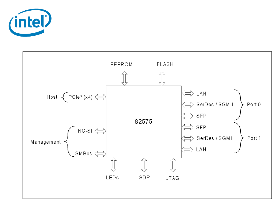
Intel® 82575EB Gigabit Ethernet Controller — Integrated 10/100/1000 Mb/s PHY
Intel® 82575EB Gigabit Ethernet Controller 324632-003
Software Developer’s Manual and EEPROM Guide Revision: 2.1
22 January 2011
Figure 1. 82575 External Interfaces
2.1.1 Integrated 10/100/1000 Mb/s PHY
The 82575 contains integrated 10/100/1000 Mb/s-capable Copper PHY's. Each of these PHY's
communicate with its MAC controllers using a standard 10/100/1000Base-T interface internal to the
component to transfer transmit and receive data. A standard MDIO interface, accessible to software via
MAC control registers, is also used to configure and monitor each PHY operation.
2.1.2 System Interface
The 82575 provides 4 lanes of PCIe* bus interface working at 2.5 GHz each, this should provide
sufficient bandwidth to support sustained dual port of 1000 Mb/s transfer rates. 48 KB of on-chip
buffering mitigates instantaneous receive bandwidth demands and eliminates transmit under-runs by
buffering the entire outgoing packet prior to transmission.
2.1.3 EEPROM Interface
The 82575 provides a four-wire direct interface to a serial EEPROM device such as the 93C46 or
compatible for storing product configuration information. Several words of the data stored in the
EEPROM are automatically accessed by the 82575, after reset, to provide pre-boot configuration data to
the 82575 before it is accessible by the host software. The remainder of the stored information is
accessed by various software modules to report product configuration, serial number and other
parameters.
Note: An EEPROM is required for normal operation.

Flash Memory Interface — Intel® 82575EB Gigabit Ethernet Controller
324632-003 Intel® 82575EB Gigabit Ethernet Controller
Revision: 2.1 Software Developer’s Manual and EEPROM Guide
January 2011 23
2.1.4 Flash Memory Interface
The 82575 provides an external serial interface to a FLASH device. Accesses to the FLASH are
controlled by the 82575 and are accessible to software as normal PCIe* reads or writes to the FLASH
memory mapping area. The 82575 supports FLASH devices with up to 512 KB of memory
2.1.5 Management Interfaces
The 82575 contains two possible interfaces to an external BMC.
• SMBus
•NC-SI
Since the manageability sideband throughput is lower than the network link throughput, the 82575
allocates an 8 KB internal buffer for incoming network packets prior to being send over the sideband
interface. Refer to the 82575 System Management Bus Interface Application Note for detailed
information about the management interface.
2.1.5.1 Software Watchdog
In some situations it might be useful to give an indication to the manageability firmware or to external
devices that the 82575 hardware or the driver is not functional. In order to provide this functionality, a
watchdog mechanism is used. This mechanism can be enabled by default, according to the EEPROM
configuration. Once the host driver is up and it determines hardware is functional, it might reset the
watchdog timer to indicate the device is functional. The software device driver then should re-arm the
timer periodically. If the timer is not re-armed after a pre-programmed timeout, an interrupt is given to
firmware and a pre-programmed SDP is raised. The SDP indication is shared between the ports.
The register controlling this feature is WDSETUP. This register enables setting the timeout period and
the activation of this mode. Both get their default from the EEPROM.
The re-arming of the timer is done by setting the WDSWSTS.Dev_functional.
If software needs to trigger the watchdog immediately because it suspects hardware is stuck, it can set
the WDSWSTS.Force_WD bit. It can also give firmware an indication if the watchdog reason using the
WDSWSTS.stuck_reason field.
The SDP that provides the watchdog indication is set using the CTRL.SDP0_WDE. In this mode the
CTRL.SDP0_IODIR should be set to output. The CTRL.SDP0_DATA bit indicates the polarity of the
indication. Setting this bit in one of the cores causes the watchdog indications of both cores to be
indicated on this SDP.
2.1.6 General-Purpose I/O (Software-Definable Pins)
The 82575 has four software-defined pins (SDP pins) per port that can be used for miscellaneous
hardware or software-controllable purposes. These pins and their function are bound to a specific LAN
device (for example, eight SDP pins might not be associated with a single LAN device). These pins can
each be individually configurable to act as either input or output pins. The default direction of each of

Intel® 82575EB Gigabit Ethernet Controller — LEDs
Intel® 82575EB Gigabit Ethernet Controller 324632-003
Software Developer’s Manual and EEPROM Guide Revision: 2.1
24 January 2011
the four pins is configurable via EEPROM as well as the default value of any pins configured as outputs.
To avoid signal contention, all four pins are set as input pins until after the EEPROM configuration is
loaded.
The use, direction, and values of SDP pins are controlled and accessed using fields in the Device Control
register (CTRL) and Extended Device Control register (CTRL_EXT).
2.1.7 LEDs
The 82575 provides four LEDs per port that can be used to indicate different traffic status. The default
setup of the LEDs is done via the EEPROM words 1Ch and 1Fh. The default setup for both ports is the
same. This setup is reflected in the LEDCTL register of each port. Each software device driver can
change its setup individually. For each of the LEDs the following parameters can be defined:
• Mode: Defines which information is reflected by this LED. The encoding is described in the LEDCTL
register.
• Polarity: Defines the polarity of the LED.
• Blink mode: should the LED blink or be stable.
In addition, the blink rate of all LEDs can be defined. The possible rates are 200 ms or 83 ms for each
phase. There is one rate for all LEDs.
2.1.8 Network Interfaces
The 82575 MAC provides a complete CSMA/CD function that supports IEEE 802.3
(10 Mb/s), 802.3u (100 Mb/s), 802.3z and 802.3ab (1000 Mb/s) implementations. The 82575 performs
all of the functions required for transmission, reception, and collision handling called out in the
standards.
Each 82575 MAC can be configured to be used as a different media interface. While the most likely
application is expected to be based on use of the internal copper PHY, the 82575 supports the following
potential configurations:
• Internal copper PHY
• External SerDes device such as an optical SerDes (SFP or onboard) or backplane connections.
• External SGMII device. This mode is used for SFP connections or external SGMII PHYs.
Selection between the various configurations is programmable via each MAC's Extended Device Control
register (CTRL_EXT.LINK_MODE bits) and defaulted via EEPROM settings.
2.2 DMA Addressing
In appropriate systems, all addresses mastered by the 82575 are 64 bits in order to support systems
that have larger than 32-bit physical addressing. Providing 64-bit addresses eliminates the need for
special segment registers.
Note: Descriptor accesses are not byte swapped.
The following example illustrates data-byte ordering. Bytes for a receive packet arrive in the order
shown from left to right.
Ethernet Addressing — Intel® 82575EB Gigabit Ethernet Controller
324632-003 Intel® 82575EB Gigabit Ethernet Controller
Revision: 2.1 Software Developer’s Manual and EEPROM Guide
January 2011 25
01 02 03 04 05 06 07 08 09 0a 0b 0c 0d 0e 0f 10 11 12 13 14 15 16 17 18 19 1a 1b 1c 1d 1e
Example 1. Byte Ordering
There are no alignment restrictions on packet-buffer addresses. The byte address for the major words
is shown on the left. The byte numbers and bit numbers for the PCIe* bus are shown across the top.
Table 1. Little Endian Data Ordering
2.3 Ethernet Addressing
Several registers store Ethernet addresses in the 82575. Two 32-bit registers make up the address: one
is called “high”, and the other is called “low”. For example, the Receive Address Register is comprised of
Receive Address High (RAH) and Receive Address Low (RAL). The least significant bit of the least
significant byte of the address stored in the register (for example, bit 0 of RAL) is the multicast bit. The
LS byte is the first byte to appear on the wire. This notation applies to all address registers, including
the flow control registers.
Figure 2 shows the bit/byte addressing order comparison between what is on the wire and the values in
the unique receive address registers.
Figure 2. Example of Address Byte Ordering
The address byte order numbering shown in Figure 2 maps to Table 2. Byte #1 is first on the wire.
Byte
Address
63 0
76543210
00807060504030201
8100f 0e0d0c0b0a09
10 18 17 16 15 14 13 12 11
18 20 1f 1e 1d 1c 1b 1a 19
Preamble & SFD Destination Address Source Address
Bit 0 of this byte is first on the wire
Destination address stored
internally as shown here
dest_addr[0]
Multicast bit
...55 D5 00 11 22 33 ...XXX00 AA
33
... 001122
2233 00AA0011
00AA

Intel® 82575EB Gigabit Ethernet Controller — Interrupt Control and Tuning
Intel® 82575EB Gigabit Ethernet Controller 324632-003
Software Developer’s Manual and EEPROM Guide Revision: 2.1
26 January 2011
Table 2. Intel® Architecture Byte Ordering
Note: The notation in this manual follows the convention shown in Table 2. For example, the
address in Table 2 indicates 00_AA_00_11_22_33h, where the first byte (00h_) is the first
byte on the wire, with bit 0 of that byte transmitted first.
2.4 Interrupt Control and Tuning
The 82575 provides a complete set of interrupts that allow for efficient software management. The
interrupt structure is designed to accomplish the following:
• Make accesses “thread-safe” by using ‘set’ and ‘clear-on-read’ rather than ‘read-modify-write’
operations.
• Correlate between related bits in different registers (for example, ICR)
• Minimize the number of interrupts needed relative to work accomplished.
• Minimize the processing overhead associated with each interrupt.
The interrupt logic consists of the interrupt registers that are described in sections 14.3.34 through
14.3.37.
Two actions minimize the number of interrupts:
1. Reducing the frequency of all interrupts
2. Accepting multiple receive packets before signaling an interrupt.
One interrupt register consolidates all interrupt information eliminating the need for multiple accesses.
Note: The 82575 supports Message Signaled Interrupts per the PCI 2.2, 2.3, and PCIe*
specifications. See Section 4.7.5.1 for details.
2.5 Hardware Acceleration Capability
The 82575 provides the ability to offload IP, TCP, and UDP checksum for transmit. The functionality
provided by these features can significantly reduce processor utilization by shifting the burden of the
functions from the driver to the hardware. Features include:
• Jumbo frame support
• Receive and transmit checksum offloading
• TCP segmentation
• Receive fragmented UDP checksum offload
• These features are briefly outlined in the following sections.
IA Byte # 1 (LSB) 2 3 4 5 6 (MSB)
Byte Value (Hex) 00 AA 00 11 22 33

Jumbo Frame Support — Intel® 82575EB Gigabit Ethernet Controller
324632-003 Intel® 82575EB Gigabit Ethernet Controller
Revision: 2.1 Software Developer’s Manual and EEPROM Guide
January 2011 27
2.5.1 Jumbo Frame Support
The 82575 supports jumbo frames to increase performance and decrease CPU utilization. By default,
the 82575 might receive packets with a maximum size of 1522 bytes. If large frame reception is
enabled by the RCTL register, the 82575 supports jumbo packet reception of up to 9018 bytes
(including CRC and headers). On the transmit size, jumbo packets are always supported by the 82575.
It is the responsibility of the software device driver to initiate jumbo packets only when it is configured
to do so.
2.5.2 Receive and Transmit Checksum Offloading
The 82575 provides the ability to offload the IP, TCP, and UDP checksum requirements from the
software device driver. For common frame types, the hardware automatically calculates, inserts, and
checks the appropriate checksum values normally handled by software.
For transmits where the 82575 is doing non-TCP segmentation, every transmitted Ethernet packet can
have two checksums calculated and inserted by the 82575. Typically these would be the IPv4 and either
TCP or UDP checksums. The software device driver specifies which portions of the packet are included
in the checksum calculations, and where the calculated values are inserted, via descriptor(s).
For receives, the hardware recognizes the packet type and performs the checksum calculations as well
as error checking automatically. Checksum and error information is provided to software via the receive
descriptor(s). Refer to Section 5.5.1 for details.
2.5.3 TCP Segmentation
The 82575 implements a TCP segmentation capability for transmits that enables the software device
driver to offload packet segmentation and encapsulation to the hardware. The software device driver
can send the 82575 the entire IP (IPv6 or IPv6), TCP or UDP message sent down by the Network
Operating System (NOS) for transmission. The 82575 segments the packet into legal Ethernet frames
and transmit them on the wire. By handling the segmentation tasks, the hardware alleviates the
software from handling some of the framing responsibilities. This reduces the overhead on the CPU for
the transmission process thus reducing overall CPU utilization.
2.5.4 Receive Fragmented UDP Checksum Offloading
The 82575 provides the ability to offload inbound fragmented UDP packet reassembly. The 82575
provides the partial checksum calculation for each incoming UDP fragment so that the software device
driver is required to sum the partial checksum words for each fragment to produce the complete
checksum. The fragmented UDP checksum offload is provided to IPv4 packets.
2.6 Buffer and Descriptor Structure
Software allocates the transmit and receive buffers, and also forms the descriptors that contain
pointers to, and the status of, those buffers. A conceptual ownership boundary exists between the
driver software and the hardware of the buffers and descriptors.

Intel® 82575EB Gigabit Ethernet Controller — Multiple Transmit Queues
Intel® 82575EB Gigabit Ethernet Controller 324632-003
Software Developer’s Manual and EEPROM Guide Revision: 2.1
28 January 2011
The software gives the hardware ownership of a queue of buffers for receives. These receive buffers
store data that the software then owns once a valid packet arrives.
For transmits, the software maintains a queue of buffers. The driver software owns a buffer until it is
ready to transmit. The software then commits the buffer to the hardware; the hardware then owns the
buffer until the data is loaded or transmitted in the transmit FIFO.
Descriptors store the following information about the buffers:
• The physical address
• The length
• Status and command information about the referenced buffer
Descriptors contain an end-of-packet field that indicates the last buffer for a packet. Descriptors also
contain packet-specific information indicating the type of packet, and specific operations to perform in
the context of transmitting a packet, such as those for VLAN or checksum offload.
2.7 Multiple Transmit Queues
The 82575 supports four transmit descriptor rings (this matches the expected number of processors on
most server platforms).
The priority between the queues can be set and specified in the memory space. Multiple transmit
queues are intended for the following usage models.
Note: If there are more processors than queues, then one queue can be used to service more
than one processor.
2.8 iSCSI Boot
This feature consists of adding an iSCSI class code to potentially replace the LAN class code of the
ports. When the system is booting, the BIOS detects this class code and runs SCSI software.
The 82575 reads two control bits out of EEPROM. Each bit affects its respective LAN class code value. If
the bit is 0b (this is the current value of the unused bits) the LAN class code remains as it is (value =
020000 = LAN). If the bit is set to 1b, the LAN class code becomes a SCSI class code (value = 010000
= SCSI). Having this functionality enables programmers to change one port (or two in specific
applications) to a SCSI device type and loads an iSCSI miniport driver for that port. This port also
functions as iSCSI HBA. Default values for these fields in the EEPROM for both ports remain as a
network class type.
In this case, the MAC address and the IP address of the port are used by the iSCSI function.
§ §

General Initialization and Reset Operation — Intel® 82575EB Gigabit Ethernet Controller
324632-003 Intel® 82575EB Gigabit Ethernet Controller
Revision: 2.1 Software Developer’s Manual and EEPROM Guide
January 2011 29
3.0 General Initialization and Reset
Operation
This section lists all necessary initializations and describes the reset commands for the 82575.
3.1 Power Up State
When the 82575 powers up, it reads the EEPROM. The EEPROM contains sufficient information to bring
the link up and configure the 82575 for manageability and/or APM wakeup. However, software
initialization is required for normal operation.
3.2 Initialization Sequence
The following sequence of commands is typically issued to the 82575 by the software device driver in
order to initialize the 82575 to normal operation. The major initialization steps are:
• Disable Interrupts - see Interrupts during initialization.
• Issue Global Reset and perform General Configuration - see Global Reset and General
Configuration.
• Setup the PHY and the link - see Link Setup Mechanisms and Control/Status Bit Summary.
• Initialize all statistical counters - see Initialization of Statistics.
• Initialize Receive - see Receive Initialization.
• Initialize Transmit - see Transmit Initialization.
• Enable Interrupts - see Interrupts During Initialization.
3.3 Interrupts During Initialization
Most drivers disable interrupts during initialization to prevent re-entrancy. Interrupts are disabled by
writing to the IMC and EIMC registers. Note that the interrupts also need to be disabled after issuing a
global reset, so a typical driver initialization flow might be:
• Disable interrupts
• Issue a Global Reset
• Disable interrupts (again)
•…

Intel® 82575EB Gigabit Ethernet Controller — Global Reset and General Configuration
Intel® 82575EB Gigabit Ethernet Controller 324632-003
Software Developer’s Manual and EEPROM Guide Revision: 2.1
30 January 2011
After the initialization completes, a typical driver enables the desired interrupts by writing to the IMS
and EIMS registers.
3.4 Global Reset and General Configuration
The 82575 initialization typically starts with a global reset that puts it into a known state and enables
the software device driver to continue the initialization sequence.
Several values in the Device Control Register (CTRL) need to be set upon power up or after an 82575
reset for normal operation.
• FD should be set per interface negotiation (if done in software), or is set by the hardware if the
interface is Auto-Negotiating. This is reflected in the Device Status Register in the Auto-Negotiating
case.
• Speed is determined via Auto-Negotiation or forced by software if the link is forced. Status
information for speed is also readable in STATUS.
• In SerDes mode, CTRL.ILOS should be set to according to the polarity of the Sig_DET signal.
Set the packet buffer allocation for transmit receive flows in the PBA register. This should be done
before RCTL.RXEN & TCTL.TXEN are set. An ordered disabling of all queues and of the Rx and Tx flows
is required before any change in the packet buffer allocation is done.
If flow control is enabled, program the FCRTL, FCRTH, FCTTV and FCRTV registers.
3.5 Receive Initialization
Program the Receive address register(s) per the station address. This can come from the EEPROM or
from any other means (for example, on some systems, this comes from the system PROM not the
EEPROM on the adapter card)
Set up the MTA (Multicast Table Array) per software by zeroing all entries initially and adding in entries
as requested.
Program RCTL with appropriate values. If initializing it at this stage, it is best to leave the receive logic
disabled (EN = 0b) until after the receive descriptor ring has been initialized. If VLANs are not used,
software should clear VFE. Then there is no need to initialize the VFTA. Select the receive descriptor
type.
The following should be done once per receive queue:
• Allocate a region of memory for the receive descriptor list.
• Receive buffers of appropriate size should be allocated and pointers to these buffers should be
stored in the descriptor ring.
• Program the descriptor base address with the address of the region.
• Set the length register to the size of the descriptor ring.
• Program PSRCTL of the queue according to the size of the buffers and the required header handling
• If header split or header replication is required for this queue, program the PSRTYPE register
according to the required headers.

Initialize the Receive Control Register — Intel® 82575EB Gigabit Ethernet Controller
324632-003 Intel® 82575EB Gigabit Ethernet Controller
Revision: 2.1 Software Developer’s Manual and EEPROM Guide
January 2011 31
• Enable the queue by setting RXDCTL.ENABLE. In the case of queue zero, the enable bit is set by
default, as such, the ring parameters should be set before RCTL.RXEN is set.
• Program the direction of packets to this queue according to the mode select in MRQC. Packets
directed to a disabled queue are dropped.
3.5.1 Initialize the Receive Control Register
To properly receive packets, the receiver should be enabled by setting RCTL.RXEN. This should be done
only after all other setup is accomplished. If software uses the Receive Descriptor Minimum Threshold
Interrupt, that value should be set.
Note: The Receive Descriptor Tail register of the queue (RDT[n]) should not be bumped until the
queue is enabled. This register must also be written after the queue is enabled and the
receiver is enabled.
3.5.2 Dynamic Queue Enabling and Disabling
Receive queues can be dynamically enabled or disabled provided the following procedure is followed:
Enabling:
• Follow the per queue initialization previously described.
• If there are still packets in the packet buffer directed to this queue according to previous settings,
they are received after the queue is re-enabled. The software device driver might check if old
packets are still in the internal packet buffer by reading the RDFPCQ# register of the queue.
Disabling:
• Disable the direction of packets to this queue.
• Disable the queue by clearing RXDCTL.ENABLE. The 82575 immediately stops to fetch and write
back descriptors from this queue. The 82575 eventually completes the storage of one buffer
allocated to this queue. Any further packet directed to this queue is dropped. If the currently
processed packet is spread over more than one buffer, all subsequent buffers are not written.
• The 82575 clears RXDCTL.ENABLE only after all pending memory accesses to the descriptor ring or
to the buffers are done. The software device drive should poll this bit before releasing the memory
allocated to this queue.
The Rx path can be disabled only after all Rx queues are disabled.
3.6 Transmit Initialization
Program the TCTL register according to the required MAC behavior.
If work in half duplex mode is expected, program the TCTL_EXT.COLD field. For internal PHY mode, the
default value is 41h. For SGMII mode, a value reflecting the 82575 and the PHY SGMII delays should be
used. A suggested value for a typical PHY is 46h for 10 Mb/s and 4Ch for 100 Mb/s.
The following should be done once per transmit queue:
• Allocate a region of memory for the transmit descriptor list.
• Program the descriptor base address with the address of the region.

Intel® 82575EB Gigabit Ethernet Controller — Dynamic Queue Enabling and Disabling
Intel® 82575EB Gigabit Ethernet Controller 324632-003
Software Developer’s Manual and EEPROM Guide Revision: 2.1
32 January 2011
• Set the length register to the size of the descriptor ring.
• Program the TXDCTL register with the desired TX descriptor write back policy. Suggested values
are:
— WTHRESH = 1b
— All other fields 0b.
• Set the queue priority using TXDCTL.Priority
• Enable the queue using TXDCTL.ENABLE (queue zero is enabled by default).
Enable the transmit path by setting TCTL. This should be done only after all other settings are done.
3.6.1 Dynamic Queue Enabling and Disabling
Transmit queues can be dynamically enabled or disabled provided the following procedure is followed:
Enabling: Follow the per queue initialization previously described.
Disabling:
• Stop storing packet for transmission in this queue.
• Wait until the head of the queue (TDH) is equal to the tail (TDT). For example, the queue is empty.
• Disable the queue by clearing TXDCTL.ENABLE.
The Tx path can be disabled only after all Tx queues are disabled.
3.7 Link Setup Mechanisms and Control/Status
Bit Summary
Note: The CTRL_EXT.LINK_MODE value should be set to the desired mode prior to the setting of
the other fields in the link setup procedures.
3.7.1 PHY Initialization
Refer to the PHY documentation for the initialization and link setup steps. The software device driver
uses the MDIC register to initialize the PHY and setup the link.
3.7.2 MAC/PHY Link Setup (CTRL_EXT.LINK_MODE =
00b)
This section summarizes the various means of establishing proper MAC/PHY link setups, differences in
MAC CTRL register settings for each mechanism, and the relevant MAC status bits. The methods are
ordered in terms of preference (the first mechanism being the most preferred).
• MAC settings automatically based on duplex and speed resolved by PHY
(CTRL.FRCDPLX = 0b, CTRL.FRCSPD = 0b)

MAC/PHY Link Setup (CTRL_EXT.LINK_MODE = 00b) — Intel® 82575EB Gigabit Ethernet
Controller
324632-003 Intel® 82575EB Gigabit Ethernet Controller
Revision: 2.1 Software Developer’s Manual and EEPROM Guide
January 2011 33
CTRL.FD - Don't care; duplex setting is established from PHY's internal indication to the MAC (FDX)
after PHY has auto-negotiated a successful link-up
CTRL.SLU - Must be set to 1b by software to enable communications between MAC and PHY
CTRL.RFCE - Must be set by software after reading flow control resolution from PHY registers
CTRL.TFCE - Must be set by software after reading flow control resolution from PHY registers
CTRL.SPEED - Don't care; speed setting is established from PHY's internal indication to the MAC
(SPD_IND) after PHY has auto-negotiated a successful link-up
STATUS.FD - Reflects the actual duplex setting (FDX) negotiated by the PHY and indicated to MAC
STATUS.LU - Reflects link indication (LINK) from PHY qualified with CTRL.SLU (set to 1b)
STATUS.SPEED - Reflects actual speed setting negotiated by the PHY and indicated to the MAC
(SPD_IND)
• MAC duplex and speed settings forced by software based on resolution of PHY
(CTRL.FRCDPLX = 1b, CTRL.FRCSPD = 1b)
CTRL.FD - Set by software based on reading PHY status register after PHY has auto-negotiated a
successful link-up
CTRL.SLU - Must be set to 1b by software to enable communications between MAC and PHY
CTRL.RFCE - Must be set by software after reading flow control resolution from PHY registers
CTRL.TFCE - Must be set by software after reading flow control resolution from PHY registers
CTRL.SPEED - Set by software based on reading PHY status register after PHY has auto-negotiated a
successful link-up.
STATUS.FD - Reflects the MAC forced duplex setting written to CTRL.FD
STATUS.LU - Reflects link indication (LINK) from PHY qualified with CTRL.SLU (set to 1b)
STATUS.SPEED - Reflects MAC forced speed setting written in CTRL.SPEED
• MAC/PHY duplex and speed settings both forced by software (fully-forced link setup)
(CTRL.FRCDPLX = 1b, CTRL.FRCSPD = 1b, CTRL.SLU = 1b)
CTRL.FD - Set by software to desired full/half duplex operation (must match duplex setting of PHY)
CTRL.SLU - Must be set to 1b by software to enable communications between MAC and PHY. PHY must
also be forced/configured to indicate positive link indication (LINK) to the MAC
CTRL.RFCE - Must be set by software to desired flow-control operation (must match flow-control
settings of PHY)
CTRL.TFCE - Must be set by software to desired flow-control operation (must match flow-control
settings of PHY)
CTRL.SPEED - Set by software to desired link speed (must match speed setting of PHY)

Intel® 82575EB Gigabit Ethernet Controller — MAC/SerDes Link Setup (CTRL_EXT.LINK_MODE =
11b)
Intel® 82575EB Gigabit Ethernet Controller 324632-003
Software Developer’s Manual and EEPROM Guide Revision: 2.1
34 January 2011
STATUS.FD - Reflects the MAC duplex setting written by software to CTRL.FD
STATUS.LU - Reflects 1b. (positive link indication LINK from PHY qualified with CTRL.SLU).
Note: Since both CTRL.SLU and the PHY link indication LINK are forced, this bit set does not
guarantee that operation of the link has been truly established.
STATUS.SPEED - Reflects MAC forced speed setting written in CTRL.SPEED.
3.7.3 MAC/SerDes Link Setup (CTRL_EXT.LINK_MODE
= 11b)
Link setup procedures using an external SerDes interface mode:
• Hardware Auto-Negotiation Enabled (PCS_LCTL.AN_ENABLE = 1b)
CTRL.FD - Ignored; duplex is set by priority resolution of PCS_ANDV and PCS_LPAB.
CTRL.SLU - Ignored; it is not possible to “force” link configuration (AN_ENABLE takes precedence)
CTRL.RFCE - Must be set by software after reading flow control resolution from PCS registers
CTRL.TFCE - Must be set by software after reading flow control resolution from PCS registers
CTRL.SPEED - Ignored; speed always 1000 Mb/s when using SGMII mode communications
STATUS.FD - Reflects hardware-negotiated priority resolution
STATUS.LU - Reflects PCS_LSTS.AN COMPLETE (Auto-Negotiation complete)
STATUS.SPEED - Reflects 1000 Mb/s speed, reporting fixed value of 10b
PCS_LCTL.FORCE_LINK - Ignored; it is not possible to "force" link configuration (AN_ENABLE takes
precedence)
PCS_LCTL.FSD - Ignored; it is not possible to "force" link configuration (AN_ENABLE takes precedence)
PCS_LCTL.FSV - Ignored; speed always 1000Mb/s when using SerDes mode communications
PCS_LCTL.FDV - Ignored; duplex is set by priority resolution of PCS_ANDV and PCS_LPAB
PCS_LCTL.FLV - Ignored; it is not possible to "force" link configuration (AN_ENABLE takes precedence)
• Software-Executed Auto-Negotiation Enabled (PCS_LCTL.AN_ENABLE = 0b)
CTRL.FD - Should be set by software to the duplex value established via software priority resolution
CTRL.SLU - Should be set by software to 1b when software Auto-Negotiation completes
CTRL.RFCE - Set by software as a result of software priority resolution
CTRL.TFCE - Set by software as a result of software priority resolution
CTRL.SPEED - Ignored; speed always 1000 Mb/s when using SerDes mode communications

MAC/SGMII Link Setup (CTRL_EXT.LINK_MODE = 10b) — Intel® 82575EB Gigabit Ethernet
Controller
324632-003 Intel® 82575EB Gigabit Ethernet Controller
Revision: 2.1 Software Developer’s Manual and EEPROM Guide
January 2011 35
STATUS.FD - Reflects the value written by software to CTRL.FD
STATUS.LU - Reflects whether loss-of-signal (LOS) from SerDes is indicated, qualified with CTRL.SLU
(set to 1b)
STATUS.SPEED - Reflects 1000 Mb/s speed, reporting fixed value of 10b
PCS_LCTL.FORCE_LINK - Must be set to 1b by software to enable communications to the SerDes
PCS_LCTL.FSD - Must be set to 1b by software to enable communications to the SerDes
PCS_LCTL.FSV - Ignored; speed always 1000 Mb/s when using SerDes mode communications.
PCS_LCTL.FDV - Should be set by software to the duplex value established via software priority
resolution
PCS_LCTL.FLV - Should be set by software to 1b when software Auto-Negotiation completes
• Forced-Link (Auto-Negotiation Skipped) (PCS_LCTL. AN ENABLE = 0b, and no software auto-
negotiation performed)
CTRL.FD - Duplex is set by software for the desired duplex mode of operation
CTRL.SLU - Must be set to 1b by software to enable communications to the SerDes
CTRL.RFCE - Set by software for the desired mode of operation
CTRL.TFCE - Set by software for the desired mode of operation
CTRL.SPEED - Ignored
STATUS.FD - Reflects the value written by software to CTRL.FD
STATUS.LU - Reflects whether loss-of-signal (LOS) from SerDes is indicated, qualified with CTRL.SLU
(set to 1b)
STATUS.SPEED - Reflects 1000 Mb/s speed, reporting fixed value of 10b
PCS_LCTL.FORCE_LINK - Must be set to 1b by software to enable communications to the SerDes
PCS_LCTL.FSD - Must be set to 1b by software to enable communications to the SerDes
PCS_LCTL.FSV - Ignored; speed always 1000 Mb/s when using SerDes mode communications.
PCS_LCTL.FDV - Duplex is set by software for the desired duplex mode of operation.
PCS_LCTL.FLV - Should be set by software to 1b to enable communications to the SerDes
3.7.4 MAC/SGMII Link Setup (CTRL_EXT.LINK_MODE
= 10b)
Link setup procedures using an external SGMII interface mode:

Intel® 82575EB Gigabit Ethernet Controller — MAC/SGMII Link Setup (CTRL_EXT.LINK_MODE =
10b)
Intel® 82575EB Gigabit Ethernet Controller 324632-003
Software Developer’s Manual and EEPROM Guide Revision: 2.1
36 January 2011
• Hardware Auto-Negotiation Enabled (PCS_LCTL. AN ENABLE = 1b,
CTRL.FRCDPLX = 0b, CTRL.FRCSPD = 0b)
CTRL.FD - Ignored; duplex is set by priority resolution of PCS_ANDV and PCS_LPAB.
CTRL.SLU - Ignored; it is not possible to “force” link configuration (AN_ENABLE takes precedence)
CTRL.RFCE - Must be set by software after reading flow control resolution from PCS registers
CTRL.TFCE - Must be set by software after reading flow control resolution from PCS registers
CTRL.SPEED - Don't care; speed setting is established from SGMII's internal indication to the MAC after
SGMII has auto-negotiated a successful link-up
STATUS.FD - Reflects hardware-negotiated priority resolution
STATUS.SPEED - Reflects actual speed setting negotiated by the SGMII and indicated to the MAC
PCS_LCTL.FORCE_LINK - Ignored; it is not possible to "force" link configuration (AN_ENABLE takes
precedence)
PCS_LCTL.FSD - Ignored; it is not possible to "force" link configuration (AN_ENABLE takes precedence)
PCS_LCTL.FSV - Ignored; speed is set by priority resolution of PCS_ANDV and PCS_LPAB
PCS_LCTL.FDV - Ignored; duplex is set by priority resolution of PCS_ANDV and PCS_LPAB
PCS_LCTL.FLV - Ignored; it is not possible to "force" link configuration (AN_ENABLE takes precedence)
• Software-Executed Auto-Negotiation Enabled (PCS_LCTL. AN ENABLE = 0b; CTRL.FRCDPLX = 1b,
CTRL.FRCSPD = 1b)
CTRL.FD - Should be set by software to the duplex value established via software priority resolution
CTRL.SLU - Should be set by software to 1b when software Auto-Negotiation completes
CTRL.RFCE - Set by software as a result of software priority resolution
CTRL.TFCE - Set by software as a result of software priority resolution
CTRL.SPEED - Set by software to desired link speed (must match speed setting of external SGMII PHY)
STATUS.FD - Reflects MAC forced speed setting written in CTRL.SPEED
STATUS.LU - Reflects whether loss-of-signal (LOS) from SerDes is indicated, qualified with CTRL.SLU
(set to 1b)
STATUS.SPEED - Reflects MAC forced speed setting written in CTRL.SPEED
PCS_LCTL.FORCE_LINK - Must be set to 1b by software to enable communications to the SGMII PHY
PCS_LCTL.FSD - Must be set to 1b by software to enable communications to the SGMII PHY
PCS_LCTL.FSV - Set by software to desired link speed (must match speed setting of external SGMII
PHY)

Reset Operation — Intel® 82575EB Gigabit Ethernet Controller
324632-003 Intel® 82575EB Gigabit Ethernet Controller
Revision: 2.1 Software Developer’s Manual and EEPROM Guide
January 2011 37
PCS_LCTL.FDV - Should be set by software to the duplex value established via software priority
resolution
PCS_LCTL.FLV - Should be set by software to 1b when software Auto-Negotiation completes
• Forced-Link (Auto-Negotiation Skipped) (PCS_LCTL. AN_ENABLE = 0b, and no software auto-
negotiation performed)
CTRL.FD - Duplex is set by software for the desired duplex mode of operation
CTRL.SLU - Must be set to 1b by software to enable communications to the SerDes
CTRL.RFCE - Set by software for the desired mode of operation
CTRL.TFCE - Set by software for the desired mode of operation
CTRL.SPEED - Set by software to desired link speed (must match speed setting of external SGMII PHY)
STATUS.FD - Reflects the value written by software to CTRL.FD
STATUS.LU - Reflects whether loss-of-signal (LOS) from SerDes is indicated, qualified with CTRL.SLU
(set to 1b)
STATUS.SPEED - Reflects MAC forced speed setting, written in CTRL.SPEED
PCS_LCTL.FORCE_LINK - Must be set to 1b by software to enable communications to the SerDes
PCS_LCTL.FSD - Must be set to 1b by software to enable communications to the SerDes
PCS_LCTL.FSV - Set by software to desired link speed (must match speed setting of external SGMII
PHY and CTRL.SPEED)
PCS_LCTL.FDV - Duplex is set by software for the desired duplex mode of operation (must match
duplex setting of external SGMII PHY and CTRL.FD)
PCS_LCTL.FLV - Must be set by software to 1b to enable communications to the SerDes
3.8 Reset Operation
The 82575’s reset sources are as follows:
PE_RST_N:
Asserting PE_RST_N indicates that both the power and the PCIe* clock sources are stable. This pin
asserts an internal reset also after a D3cold exit. Most units are reset on the rising edge of PE_RST_N.
The only exception is the GIO unit, which is kept in reset while PE_RST_N is deasserted (level).
Inband PCIe* Reset:
The 82575 generates an internal reset in response to a Physical layer message from the PCIe* or when
the PCIe* link goes down (entry to Polling or Detect state). This reset is equivalent to PCI reset in
previous (PCI) gigabit LAN controllers.

Intel® 82575EB Gigabit Ethernet Controller — Reset Operation
Intel® 82575EB Gigabit Ethernet Controller 324632-003
Software Developer’s Manual and EEPROM Guide Revision: 2.1
38 January 2011
D3hot to D0 Transition:
This is also known as ACPI Reset. The 82575 generates an internal reset on the transition from D3hot
power state to D0 (caused after configuration writes from D3 to D0 power state). Note that this reset is
per function and resets only the function that transitioned from D3hot to D0.
Software Reset:
Software can reset the 82575 by writing the Device Reset bit of the Device Control register (CTRL.RST).
The 82575 re-reads the per-function EEPROM fields after a software reset. Bits that are normally read
from the EEPROM are reset to their default hardware values. Note that this reset is per function and
resets only the function that received the software reset. PCI Configuration space (configuration and
mapping) of the 82575 is unaffected. Prior to issuing a software reset the software device driver needs
to operate the master disable algorithm.
Force TCO:
This reset is generated when manageability logic is enabled. It is only be generated if the Reset on
Force TCO bit of the EEPROM's Management Control word is 1b. In pass through mode it is generated
when receiving a ForceTCO SMB command with bit 1 or bit 7 set. EEPROM Reset:
Writing a 1b to the EEPROM Reset bit of the Extended Device Control Register (CTRL_EXT.EE_RST)
causes the 82575 to re-read the per-function configuration from the EEPROM, setting the appropriate
bits in the registers loaded by the EEPROM.
PHY Reset:
Software can write a 1b to the PHY Reset bit of the Device Control Register (CTRL.PHY_RST) to reset
the internal PHY. The firmware must configure the PHY following a PHY Reset.
The procedure for resetting the PHY by software is as follows:
1. Take PHY ownership using the software semaphore (SWSM.SWESMBI - 05B50h, bit 1 and
SY_FW_SYNC.SW_PHY_SM0/1 - 05B5Ch, bit 1/2).
2. Drive PHY reset.
3. Wait 10 ms
4. Release PHY reset in the CTRL register.
5. Release PHY and EEPROM ownership using the software semaphore (SWSM.SWESMBI - 05B50h, bit
1 and SY_FW_SYNC. SW_PHY_SM0/1, SY_FW_SYNC. SW_EEP_SM - 05B5Ch, bit 1/2/0).
6. Wait for the CFG_DONE (EEMNGCTL.CFG_DONE - 1010h, bit 18).
7. Start configuring the PHY.
Note: Refer to Section 14.0 for a description of software/firmware semaphore usage.
The resets affect the registers and logic listed in Table 3.

Reset Operation — Intel® 82575EB Gigabit Ethernet Controller
324632-003 Intel® 82575EB Gigabit Ethernet Controller
Revision: 2.1 Software Developer’s Manual and EEPROM Guide
January 2011 39
Table 3. 82575 Reset Effects
Notes:
1. If AUX_POWER = 0b the Wakeup Context is reset (PME_Status and PME_En bits should be 0b at
reset if the 82575 does not support PME from D3cold).
2. The firmware must configure the PHY after any PHY reset.
3. Link reset clears the Receive Configuration Word (RXCW).
4. The following register fields do not follow the previously stated general rules:
Reset Activation Internal_Power_O
n_Reset PE_
RST_N In-Band
PCIe* D3hot
to D0 SW Force
TCO EE PHY Notes
LTSSM (PCIe* back
to detect/polling)
XXX
PCIe* Link data
path
XXX
Read EEPROM (Per
Function)
XXXX
Read EEPROM
(Complete Load)
XXX
PCI Configuration
Registers RO
XXX 4
PCI Configuration
Registers RW
XXXX
PCIe* local
registers
XXX 5
Data path X X X X X X
Wake Up (PM)
Context
X Note 1 5
Wake Up Control
Register
X 6
Wake Up Status
Registers
X 7
Rule Checker
Tables
X
Manageability
Control Registers
X 8
Firmware (MMS
Unit)
X
Wake-Up
Management
Registers
X X X X X X 4, 9
Memory
Configuration
Registers
÷÷÷÷÷÷ 4
PHY/SerDes PHY ÷ ÷ ÷ ÷ ÷ ÷ 2
Strapping Pins ÷ ÷ ÷

Intel® 82575EB Gigabit Ethernet Controller — Reset Operation
Intel® 82575EB Gigabit Ethernet Controller 324632-003
Software Developer’s Manual and EEPROM Guide Revision: 2.1
40 January 2011
a. SDP0_IODIR, SDP1_IODIR, SDP2_IODIR, SDP3_IODIR - reset on Internal_Power_On_Reset
only. Any EEPROM auto-load resets these fields to the values in the EEPROM.
b. Packet Buffer Allocation (PBA) - reset on Internal_Power_On_Reset only.
c. Packet Buffer Size (PBS) - reset on Internal_Power_On_Reset only.
d. LED configuration registers
e. The Aux Power Detected bit in the PCIe* Device Status register is reset on
Internal_Power_On_Reset and GIO Power Good only
f. FLA - reset on Internal_Power_On_Reset only.
5. The following registers are part of this group:
a. SWSM
b. GCR (only part of the bits; see Section 14.0)
c. FUNCTAG
d. GSCL_1/2/3/4
e. GSCN_0/1/2/3
f. SW_FW_SYNC (only part of the bits; see Section 14.0)
6. The Wake Up Context is defined in the PCI Bus Power Management Interface Specification (Sticky
bits). It includes:
a. PME_En bit of the Power Management Control/Status Register (PMCSR).
b. PME_Status bit of the Power Management Control/Status Register (PMCSR).
c. Aux_En in the PCIe* registers
d. The device Requester ID (since it is required for the PM_PME TLP).
e. The shadow copies of these bits in the Wakeup Control Register are treated identically.
7. Refers to bits in the Wake Up Control Register that are not part of the Wake-Up Context (the
PME_En and PME_Status bits).
8. The Wake Up Status Registers include the following:
a. Wake Up Status Register
b. Wake Up Packet Length.
c. Wake Up Packet Memory.
9. The manageability control registers refer to the following registers:
a. MANC - 5820h
b. MFUTP01-7 - 05030h - 504Ch
c. MFVAL - 05824h
d. MANC2H - 5860h
e. MAVTV1-7 - 0x5010 - 0x502C
f. MDEF0-7 - 890h - 58AC
g. MIPAF0-15 - 58B0h - 58ECh
10. MMAH/MMAL0-3 - 5910h - 592Ch
11. FWSM
Note: For detailed manageability control register information, refer to the Intel® 82575 TCO/
System Manageability Interface Application Note.
12. The Wake-up Management Registers include the following:
a. Wake Up Filter Control.

PHY Behavior During a Manageability Session: — Intel® 82575EB Gigabit Ethernet Controller
324632-003 Intel® 82575EB Gigabit Ethernet Controller
Revision: 2.1 Software Developer’s Manual and EEPROM Guide
January 2011 41
b. IP Address Valid.
c. IPv4 Address Table
d. IPv6 Address Table
e. Flexible Filter Length Table
f. Flexible Filter Mask Table
13. The Other Configuration Registers includes:
— General Registers
— Interrupt Registers
— Receive Registers
— Transmit Registers
— Statistics Registers
— Diagnostic Registers
Of these registers, MTA[n], VFTA[n], WUPM[n], FFMT[n], FFVT[n], TDBAH/TDBAL, and RDBAH/RDVAL
registers have no default value. If the functions associated with the registers are enabled they must be
programmed by software. Once programmed, their value is preserved through all resets as long as
power is applied to the 82575.
Note: In situations where the 82575 is reset using the software reset CTRL.RST, the TX data lines
are forced to all zeros. This causes a substantial number of symbol errors to be detected by
the link partner.
3.8.1 PHY Behavior During a Manageability Session:
During some manageability sessions (for example a IDER or SOL session as initiated by an external
BMC), the platform is reset so that it boots from a remote media. This reset must not cause the
Ethernet link to drop since the manageability session will be lost. Also, the Ethernet link should be kept
on continuously during the session for the same reasons. The 82575 limits the cases in which the
internal PHY would restart the link, by masking two types of events from the internal PHY:
• PE_RST_N and PCIe* resets (in-band and link drop) do not reset the PHY during such a
manageability session
• The PHY does not change link speed as a result of a change in power management state to avoid
link loss. For example, the transition to D3hot state is not propagated to the PHY.
— Note that if main power is removed, the PHY is allowed to react to the change in power state
(the PHY might respond in link speed change). The motivation for this exception is to reduce
power when operating on auxiliary power by reducing link speed.
The capability described in this section is disabled by default on Internal_Power_On_Reset. The
Keep_PHY_Link_Up_En bit in the EEPROM must be set to 1b to enable it. Once enabled, the feature is
enabled until the next Internal_Power_On_Reset (the 82575 does not revert to the hardware default
value on PE_RST_N, PCIe* reset, or any other reset but Internal_Power_On_Reset).
When the Keep_PHY_Link_Up bit (veto bit) in the MANC register is set, the following behaviors are
disabled:
• The PHY is not reset on PE_RST_N and PCIe* resets (in-band and link drop). Other reset events are
not affected: Internal_Power_On_Reset, Device Disable, Force TCO, and PHY reset by software.
• The PHY does not change its power state. As a result link speed does not change.
• The 82575 does not initiate configuration of the PHY to avoid losing link.

Intel® 82575EB Gigabit Ethernet Controller — Initialization of Statistics
Intel® 82575EB Gigabit Ethernet Controller 324632-003
Software Developer’s Manual and EEPROM Guide Revision: 2.1
42 January 2011
The Keep_PHY_Link_Up bit is set by the BMC through a command on the sideband interface. It is
cleared by the external BMC (again, through a command on the sideband interface) when the
manageability session ends. Once the Keep_PHY_Link_Up bit is cleared, the PHY updates its Dx state
and acts accordingly (negotiates its speed).
The Keep_PHY_Link_Up bit is also cleared on de-assertion of the MAIN_PWR_OK input pin.
MAIN_PWR_OK must be de-asserted at least 1 ms before power drops below its 90% value. This allows
enough time to respond before auxiliary power takes over.
The Keep_PHY_Link_Up bit is a R/W bit and can be accessed by host software, but software is not
expected to clear the bit. The bit is cleared in the following cases:
• On Internal_Power_On_Reset
• When the BMC resets or initializes it
• On de-assertion of the MAIN_PWR_OK input pin. The BMC should set the bit again if it wishes to
maintain speed on exit from Dr state.
3.9 Initialization of Statistics
Statistics registers are hardware-initialized to values as detailed in each particular register’s
description. The initialization of these registers begins upon transition to D0active power state (when
internal registers become accessible, as enabled by setting the Memory Access Enable of the PCIe*
Command register) and is guaranteed to complete within 1 μs of this transition. Access to statistics
registers prior to this interval might return indeterminate values.
All of the statistical counters are cleared on read and a typical software device driver reads them
(making them zero) as a part of the initialization sequence.
§ §

EEPROM and Flash Interface — Intel® 82575EB Gigabit Ethernet Controller
324632-003 Intel® 82575EB Gigabit Ethernet Controller
Revision: 2.1 Software Developer’s Manual and EEPROM Guide
January 2011 43
4.0 EEPROM and Flash Interface
This section describes the EEPROM and Flash interfaces supported by 82575.
4.1 EEPROM Device
The 82575 uses an EEPROM device to store product configuration information. The EEPROM is divided
into three general regions:
•Hardware Accessed — Loaded by the 82575 after power-up, PCI reset de-assertion, a D3 to D0
transition, or a software commanded EEPROM read (CTRL_EXT.EE_RST).
• Manageability Firmware Accessed
— In Pass-Through (PT) mode, loaded by the 82575 in PT mode after power up or a firmware
reset. Refer to the Intel® 82575 GbE Controller System Manageability Interface Application
Note for more information.
•Software Accessed — Used by software only. These registers are listed in this document for
convenience and are only for software and are ignored by the 82575.
The EEPROM interface supports Serial Peripheral Interface (SPI) mode 0 and expects the EEPROM to be
capable of 2 MHz operation.
The 82575 is compatible with many sizes of 4-wire serial EEPROM devices.If PT mode functionality
(SMBus or NC-SI) is desired, a 32 KB (256 Kb) serial SPI-compatible EEPROM is recommended. If no
manageability mode is desired, a 16 KB (128 Kb) serial SPI-compatible EEPROM can be used. All
EEPROMs are accessed in 16-bit words although the EEPROM is designed to also accept 8-bit data
accesses.
The 82575 automatically determines the address size to be used with the SPI EEPROM it is connected
to and sets the EEPROM Size field of the EEPROM/Flash Control (EEC) and Data Register
(EEC.EE_ADDR_SIZE; bit 10). Software uses this size to determine the EEPROM access method. The
exact size of the EEPROM is stored within one of the EEPROM words.
Note: The different EEPROM sizes have two different numbers of address bits (8 bits or 16 bits).
As a result, they must be accessed with a slightly different serial protocol. Software must be
aware of this if it accesses the EEPROM using direct access.
4.1.1 Software Accesses
The 82575 provides two different methods for software access to the EEPROM. It can either use the
built-in controller to read the EEPROM or access the EEPROM directly using the EEPROM’s 4-wire
interface.

Intel® 82575EB Gigabit Ethernet Controller — Signature and CRC Fields
Intel® 82575EB Gigabit Ethernet Controller 324632-003
Software Developer’s Manual and EEPROM Guide Revision: 2.1
44 January 2011
Software can use the EEPROM Read register (EERD) to cause the 82575 to read a word from the
EEPROM that the software can then use. To do this, software writes the address to read into the Read
Address field (EERD.ADDR; bits 15:2) and simultaneously writes a 1b to the Start Read bit
(EERD.START; bit 0). The 82575 then reads the word from the EEPROM, sets the Read Done bit
(EERD.DONE; bit 1), and puts the data in the Read Data field (EERD.DATA; bits 31:16). Software can
poll the EEPROM Read register until it sees the Read Done bit set, then use the data from the Read Data
field. Any words read this way are not written to the 82575’s internal registers.
Software can also directly access the EEPROM’s 4-wire interface through the EEPROM/Flash Control
register (EEC). It can use this for reads, writes, or other EEPROM operations.
To directly access the EEPROM, software should follow these steps:
1. Write a 1b to the EEPROM Request bit (EEC.EE_REQ; bit 6).
2. Read the EEPROM Grant bit (EEC.EE_GNT; bit 7) until it becomes 1b. It remains 0b as long as the
hardware is accessing the EEPROM.
3. Write or read the EEPROM using the direct access to the 4-wire interface as defined in the EEPROM/
Flash Control & Data register (EEC). The exact protocol used depends on the EEPROM placed on the
board and can be found in the appropriate datasheet.
4. Write a 0b to the EEPROM Request bit (EEC.EE_REQ; bit 6).
Finally, software can cause the 82575 to re-read part of the hardware accessed fields of the EEPROM
(setting the 82575’s internal registers appropriately) by writing a 1b to the EEPROM Reset bit of the
Extended Device Control Register (CTRL_EXT.EE_RST; bit 13).
Note: If the EEPROM does not contain a valid signature, the 82575 assumes 16-bit addressing. In
order to access an EEPROM requiring 8-bit addressing, software must use the direct access
mode.
4.1.2 Signature and CRC Fields
The only way the 82575 can discover whether an EEPROM is present is by trying to read the EEPROM.
The 82575 first reads the EEPROM Sizing & Protected field Word at address 12h. The 82575 checks the
signature value for bits 15 and 14. If bit 15 is 0b and bit 14 is 1b, it considers the EEPROM to be
present and valid and reads additional EEPROM words and programs its internal registers based on the
values read. Otherwise, it ignores the values it read from that location and does not read any other
words.
4.1.3 EEPROM Recovery
The EEPROM contains fields that if programmed incorrectly might affect the functionality of 82575. The
impact can range from incorrectly setting a function like LED programming, disabling an entire feature
like no manageability or link disconnection, to the inability to access the 82575 via the regular PCIe*
interface.
The 825785 implements a mechanism that enables a recovery from a faulty EEPROM no matter what
the impact is by using an SMBus message that instructs the firmware to invalidate the EEPROM.

Protected EEPROM Space — Intel® 82575EB Gigabit Ethernet Controller
324632-003 Intel® 82575EB Gigabit Ethernet Controller
Revision: 2.1 Software Developer’s Manual and EEPROM Guide
January 2011 45
This mechanism uses an SMBus message that the firmware is able to receive in all modes, no matter
what the content of the EEPROM is (even in diagnostic mode). After receiving this kind of message, the
firmware clears the signature of the EEPROM in word 12h bit 15/14 to 00b. Afterwards, the BIOS/
operating system initiates a reset to force an EEPROM auto-load process that fails and enables access
to the 82575.
Firmware is programmed to receive such a command only from a PCIe* reset until one of the functions
changes it status from D0u to D0a. Once one of the functions switches to D0a, it can be safely assumed
that the 82575 is accessible to the host and there is no more need for this function. This reduces the
possibility of malicious software to use this command as a back door and limits the time the firmware
must be active in non-manageability mode.
If the firmware is programmed not to do any other function apart from answering to this command, it
can request clock gating immediately after one of the functions changes it status from D0u to D0a. If
the system goes back down to D0u from D0a, it is undefined whether firmware supports the EEPROM
recovery command.
The Command is sent on a fixed SMBus address of C8h. The format of the command is SMBus Write
Data Byte as follows:
Note: This solution requires a controllable SMBus connection to the 82575.
If more than one 82575 is in a state to accept this solution, then all the 82575s on the
board ACKs this command and accepts it. An 82575 supporting this mode should not ACK
this command if it is not in D0u state.
The 82575 is guaranteed to accept the command on the SMBus interface and on address
C8h; however, it might be accepted on other configured interfaces and addresses as well.
After receiving a release EEPROM command, firmware should keep its current state. It is the
responsibility of the programmer updating the EEPROM to send a firmware reset, if required, after the
full EEPROM update process completes.
4.1.4 Protected EEPROM Space
The 82575 provides to the host a mechanism for a hidden area in the EEPROM. The hidden area cannot
be accessed via the EEPROM registers in the CSR space. It can be accessed only by the Manageability
(MNG) subsystem. For more information on the MNG subsystem, refer to the 82575 TCO/System
Manageability Interface Application Note.
A mechanism to protect part of the EEPROM from host writes is also provided. This mechanism is
controlled by words 2Dh and 2Ch. These words control the start and the end of the read only area.
4.1.5 Initial EEPROM Programming
In most applications, initial EEPROM programming is done directly on the EEPROM pins. Nevertheless, it
is desirable to enable existing software utilities (accessing the EEPROM via the host interface) to initially
program the whole EEPROM without breaking the protection mechanism. Following a power-up
Function Command Data Byte
Release EEPROM C7h AAh

Intel® 82575EB Gigabit Ethernet Controller — Activating the Protection Mechanism
Intel® 82575EB Gigabit Ethernet Controller 324632-003
Software Developer’s Manual and EEPROM Guide Revision: 2.1
46 January 2011
sequence, the 82575 reads the hardware initialization words in the EEPROM. If the signature in word
12h does not equal 01b the EEPROM is assumed as non-programmed. There are two effects for non-
valid signature:
• The 82575 stops reading EEPROM data and sets the relevant registers to default values.
• The 82575 enables access to any location in the EEPROM via the EEPROM CSR registers.
4.1.6 Activating the Protection Mechanism
Following an 82575 initialization, it reads the EEPROM. It then turns on the protection mechanism if
word 12h [15:14] contains a valid signature (equals 01b) and bit 4 in word 12h is set (enable
protection). Once the protection mechanism is turned on, words 12h, 2Ch, and 2Dh become write-
protected and the area that is defined by word 12h becomes hidden (for example, read/write
protected) and the area defined by word 2Ch and 2Dh becomes write protected.
Note: No matter what the read only protected area is, words 30h:3Fh (used by the PXE driver)
are writeable unless defined as hidden.
4.1.7 Non Permitted Accesses to Protected Areas in
the EEPROM
This section refers to EEPROM accesses via the EEC (bit banging) or EERD (parallel read access)
registers. Following a write access to the write protected areas in the EEPROM, the hardware responds
properly on the PCIe* bus, but does not initiate any access to the EEPROM. Following a read access to
the hidden area in the EEPROM (as defined by word 12h), the hardware does not access the EEPROM
and returns meaningless data to the host.
Note: Using bit banging, the SPI EEPROM can be accessed in a burst mode. For example,
providing an opcode address and then reading or writing data for multiple bytes. The
hardware inhibits an attempt to access the protected EEPROM locations even in burst
accesses.
Software should not access the EEPROM in a Burst Write mode starting in a non protected area and
continue to a protected one. In such a case, it is not guaranteed that the write access to any area ever
takes place.
4.1.8 EEPROM-Less Support
The 82575 loads information from the EEPROM non-volatile memory storage into the device registers
during the power-up sequence. If an EEPROM is not present, either by design or by fault, some of the
device registers might not be tuned for normal operation. It is required that the following script be run
immediately after an 82575 reset and before normal operation if an EEPROM is not detected.
Note: These actions are presented without comment because most of the settings involved are
not customer tunable. They must be performed in order, and the loader function is included
as follows. The example code is designed to be extensible to include other hardware
families.
Definitions:
u32 is unsigned 32 bit value,

EEPROM-Less Support — Intel® 82575EB Gigabit Ethernet Controller
324632-003 Intel® 82575EB Gigabit Ethernet Controller
Revision: 2.1 Software Developer’s Manual and EEPROM Guide
January 2011 47
s32 is signed 32 bit value,
u8 is unsigned 8 bit value.
#define E1000_CCMCTL 0x05B48 /* CCM Control Register */
#define E1000_GIOCTL 0x05B44 /* GIO Analog Control Register */
#define E1000_SCCTL 0x05B4C /* PCIc PLL Cfg Register */
#define E1000_SCTL 0x00024 /* SerDes Control */
#define E1000_EECD 0x00010 /* EEPROM Control */
#define E1000_EECD_PRES 0x00000100 /* NVM Present */
#define E1000_GEN_CTL_READY 0x80000000
#define E1000_GEN_CTL_ADDRESS_SHIFT 8
#define E1000_GEN_POLL_TIMEOUT 640
Error codes are not required to be standard; programmers can define them as needed.
/* Is the EEPROM present? If not then run the tuning script*/
if ((E1000_READ_REG(hw, E1000_EECD) & E1000_EECD_PRES) == 0)
if (hw->mac.type == e1000_82575) {
/* SerDes configuration via SERDESCTRL */
e1000_write_8bit_ctrl_reg(E1000_SCTL, 0x00, 0x0C);
e1000_write_8bit_ctrl_reg(E1000_SCTL, 0x01, 0x78);
e1000_write_8bit_ctrl_reg(E1000_SCTL, 0x1B, 0x23);
e1000_write_8bit_ctrl_reg(E1000_SCTL, 0x23, 0x15);
/* CCM configuration via CCMCTL register */
e1000_write_8bit_ctrl_reg(E1000_CCMCTL, 0x14, 0x00);
e1000_write_8bit_ctrl_reg(E1000_CCMCTL, 0x10, 0x00);
/* PCIe lanes configuration */
e1000_write_8bit_ctrl_reg(E1000_GIOCTL, 0x00, 0xEC);
e1000_write_8bit_ctrl_reg(E1000_GIOCTL, 0x61, 0xDF);
e1000_write_8bit_ctrl_reg(E1000_GIOCTL, 0x34, 0x05);

Intel® 82575EB Gigabit Ethernet Controller — EEPROM-Less Support
Intel® 82575EB Gigabit Ethernet Controller 324632-003
Software Developer’s Manual and EEPROM Guide Revision: 2.1
48 January 2011
e1000_write_8bit_ctrl_reg(E1000_GIOCTL, 0x2F, 0x81);
/* PCIe PLL Configuration */
e1000_write_8bit_ctrl_reg(E1000_SCCTL, 0x02, 0x47);
e1000_write_8bit_ctrl_reg(E1000_SCCTL, 0x14, 0x00);
e1000_write_8bit_ctrl_reg(E1000_SCCTL, 0x10, 0x00);
}
}
/**
* e1000_write_8bit_ctrl_reg - Write a 8bit CTRL register
* INPUTS
* reg: 32-bit register offset such as E1000_SCTL
* offset: register offset to write to
* data: data to write at register offset
*
* Writes an address/data control type register. There are several of these
* and they all have the format address << 8 | data and bit 31 is polled for
* completion.
**/
s32
e1000_write_8bit_ctrl_reg (u32 reg, u32 offset, u8 data)
{
u32 i, regvalue = 0;
s32 ret_val = E1000_SUCCESS;
/* Set up the address and data */
regvalue = ((u32)data) | (offset << E1000_GEN_CTL_ADDRESS_SHIFT);
E1000_WRITE_REG(reg, regvalue);

Flash Interface Operation — Intel® 82575EB Gigabit Ethernet Controller
324632-003 Intel® 82575EB Gigabit Ethernet Controller
Revision: 2.1 Software Developer’s Manual and EEPROM Guide
January 2011 49
/* Poll the ready bit to see if the MDI read completed */
for (i = 0; i < E1000_GEN_POLL_TIMEOUT; i++) {
usec_delay(5);
regvalue = E1000_READ_REG(reg);
if (regvalue & E1000_GEN_CTL_READY)
break;
}
if (!(regvalue & E1000_GEN_CTL_READY)) {
DEBUGOUT1("Reg %08x did not indicate ready\n", reg);
ret_val = -E1000_ERR_PHY;
}
return ret_val;
}
4.2 Flash Interface Operation
The 82575 provides two different methods for software access to the Flash.
Using legacy Flash transactions, the Flash is read from, or written to, each time the host processor
performs a read or a write operation to a memory location that is within the FLASH address mapping or
at boot via accesses in the space indicated by the Expansion ROM Base Address register. All accesses to
the Flash require the appropriate command sequence for the 82575 used. Refer to the specific Flash
data sheet for more details on reading from or writing to Flash.
Accesses to the Flash are based on a direct decode of processor accesses to a memory window defined
in either:
1. The 82575’s Flash Base Address register (PCIe* Control register at offset 14h or 18h).
2. A certain address range of the IOADDR register defined by the IO Base Address register (PCIe*
Control register at offset 18h or 20h).
3. The Expansion ROM Base Address register (PCIe* Control register at offset 30h).
The 82575 controls accesses to the Flash when it decodes a valid access.
Note: Flash read accesses must always be assembled by the 82575 each time the access is
greater than a byte-wide access.
The 82575 byte reads or writes to the Flash take on the order of 2 s. The 82575 continues
to issue retry accesses during this time.
The 82575 supports only byte writes to the Flash.
Another way for software to access the Flash is directly using the Flash's 4-wire interface through the
Flash Access register (FLA). It can use this for reads, writes, or other Flash operations (accessing the
Flash status register, erase, etc.).

Intel® 82575EB Gigabit Ethernet Controller — Flash Write Control
Intel® 82575EB Gigabit Ethernet Controller 324632-003
Software Developer’s Manual and EEPROM Guide Revision: 2.1
50 January 2011
To directly access the Flash, software needs to:
1. Write a 1b to the Flash Request bit (FLA.FL_REQ)
2. Read the Flash Grant bit (FLA.FL_GNT) until it = 1b. It remains 0b as long as there are other
accesses to the Flash.
3. Write or read the Flash using the direct access to the 4-wire interface as defined in the Flash Access
register (FLA). The exact protocol used depends on the Flash placed on the board and can be found
in the appropriate datasheet.
4. Write a 0b to the Flash Request bit (FLA.FL_REQ).
4.2.1 Flash Write Control
The Flash is write controlled by the FWE bits in the EEPROM/FLASH Control and Data register
(EEC.FWE). Note that attempts to write to the Flash device when writes are disabled (FWE = 10b)
should not be attempted. Behavior after such an operation is undefined and can result in component
and/or system hangs.
After sending a one byte write to the Flash, software checks if it can send the next byte to write (check
if the write process in the Flash had finished) by reading the Flash Access register. If the bit
(FLA.FL_BUSY) in this register is set, the current write did not finish. If bit (FLA.FL_BUSY) is cleared,
then software can continue and write the next byte to the Flash.
4.2.2 Flash Erase Control
When software needs to erase the Flash, it sets bit FLA.FL_ER in the Flash Access register to 1b (Flash
Erase) and then set bit EEC.FWE in the EEPROM/Flash Control register to 0b.
Hardware gets this command and sends the erase command to the Flash. Note that the erase process
completes automatically. Software should wait for the end of the erase process before any further
access to the Flash. This can be checked by using the Flash Write control mechanism.
The op-code used for erase operation is defined in the FLASHOP register.
Note: Sector erase by software is not supported. In order to delete a sector, the serial (bit bang)
interface should be used.
4.3 Shared EEPROM
The 82575 uses a single EEPROM device to configure hardware default parameters for both LAN devices
including Ethernet Individual Addresses (IA), LED behaviors, receive packet-filters for manageability,
and wakeup capability). Certain EEPROM words are used to specify hardware parameters that are LAN
device-independent (such as those which affect circuits behavior). Other EEPROM words are associated
with a specific LAN device. Both LAN devices access the EEPROM to obtain their respective configuration
settings.
4.3.1 EEPROM Deadlock Avoidance
The EEPROM is a shared resource between four clients:

EEPROM Map Shared Words — Intel® 82575EB Gigabit Ethernet Controller
324632-003 Intel® 82575EB Gigabit Ethernet Controller
Revision: 2.1 Software Developer’s Manual and EEPROM Guide
January 2011 51
• Hardware auto read.
• Accesses of port 0 LAN driver.
• Accesses of port 1 LAN driver.
• Firmware accesses.
All clients can access the EEPROM using parallel access, where hardware implements the actual access
to the EEPROM. Hardware can also schedule these accesses so that all clients get served without
starvation.
However, software and firmware clients can access the EEPROM using bit banging. In this case, there is
a request/grant mechanism that locks the EEPROM to the exclusive usage of one client. If this client is
stuck without releasing the lock, the other clients can no longer access the EEPROM. To avoid this, the
82575 implements a timeout mechanism that releases the grant from a client that did not toggle the
EEPROM bit-bang interface for more than two seconds.
Consequently, if an agent that was granted access to the EEPROM for bit-bang access did not toggle,
the bit bang interface for 500 ms. The agent should check if it still owns the interface before continuing
the bit-banging.
4.3.2 EEPROM Map Shared Words
The EEPROM map lists those words configuring either LAN devices or the entire 82575 as LAN 0/LAN 1
Both. Those words configuring a specific LAN’s device parameters are identified as either LAN 0 or LAN
1.
The following EEPROM words warrant additional notes specifically related to dual-LAN support:
4.4 Shared FLASH
The 82575 provides an interface to an external serial Flash/ROM memory device. This Flash/ROM
device can be mapped into memory and/or I/O address space for each LAN device through the use of
Base Address Registers (BARs). Bit 13 of the EEPROM Initialization Control Word 3 associated with each
LAN device selectively disables/enables whether the Flash can be mapped for each LAN device by
controlling the BAR register advertisement and write ability.
Ethernet Address (IA)
(LAN 0/LAN 1 shared)
The EEPROM specifies the IA associated with the LAN 0 device and used as the hardware
default of the Receive Address registers for that device. The hardware-default IA for the
LAN 1 device is automatically determined by the same EEPROM word and is set to the value
of {IA LAN 0 XOR 010000000000h}.
Initialization Control 1,
Initialization Control 2
(LAN 0/LAN 1 shared)
These EEPROM words specify hardware-default values for parameters that apply a single
value to both LAN devices, such as link configuration parameters required for auto-
negotiation, wakeup settings, PCI/PCI-X bus advertised capabilities, etc.
Initialization Control 3
(LAN 0, LAN 1 unique)
This EEPROM word configures default values associated with each LAN device's hardware
connections, including which link mode (internal PHY) is used with this LAN device. Because
a separate EEPROM word configures the defaults for each LAN, extra care must be taken to
ensure that the EEPROM image does not specify a resource conflict.

Intel® 82575EB Gigabit Ethernet Controller — Flash Access Contention
Intel® 82575EB Gigabit Ethernet Controller 324632-003
Software Developer’s Manual and EEPROM Guide Revision: 2.1
52 January 2011
4.4.1 Flash Access Contention
The 82575 implements internal arbitration between Flash accesses initiated through the LAN 0 device
and those initiated through the LAN 1 device. If accesses from both LAN devices are initiated during the
same approximate size window, the first one is served first and only then the next one. Note that the
82575 does not synchronize between the two entities accessing the Flash though contentions caused
from one entity reading and the other modifying the same locations is possible.
To avoid this contention, accesses from both LAN devices should be synchronized using external
software synchronization of the memory or I/O transactions responsible for the access. It might be
possible to ensure contention-avoidance simply by nature of software sequence.
4.4.2 Flash Deadlock Avoidance
The flash is a shared resource between the following clients:
• Accesses of port 0 LAN driver
• Accesses of port 1 LAN driver
• BIOS Parallel access via expansion ROM mechanism
• Firmware accesses
All clients can access the EEPROM using parallel access, where hardware implements the actual access
to the flash. Hardware can schedule these accesses so that all the clients get served without starvation.
However, software and hardware clients can access the serial flash using bit banging. In this case, there
is a request/grant mechanism that locks the serial flash to the exclusive usage of one client. If this
client is stuck without releasing the lock, the other clients cannot access the flash. In order to avoid
this, the 82575 implements a timeout mechanism, which releases the grant from a client that did not
toggle the flash bit-bang interface for more than two seconds.
Consequently, if an agent that was granted access to the flash for bit-bang access did not toggle the
bit-bang interface for 500 ms, it should check if it still owns the interface before continuing bit banging.
This mode is enabled by bit 5 in word 0Ah of the EEPROM.
4.5 EEPROM Map
Table 4 lists the EEPROM map for the 82575.
Table 4. 82575 EEPROM Map
Word Used
By1High Byte (15:8) Low Byte (7:0) Image
Value LAN 0/1
00h HW Ethernet Address Byte 2 Ethernet Address Byte 1 IA(2,1) Both
01h HW Ethernet Address Byte 4 Ethernet Address Byte 3 IA(4,3) Both
02h HW Ethernet Address Byte 6 Ethernet Address Byte 5 IA(6,5) Both
03h:
07h
SW Compatibility (High Byte) Compatibility (Low Byte) 0000h Both
08h SW PBA Byte 1 PBA Byte 2

EEPROM Map — Intel® 82575EB Gigabit Ethernet Controller
324632-003 Intel® 82575EB Gigabit Ethernet Controller
Revision: 2.1 Software Developer’s Manual and EEPROM Guide
January 2011 53
09h SW PBA Byte 3 PBA Byte 4
0Ah HW Initialization Control 1 All
0Bh HW Subsystem ID Both
0Ch HW Subsystem Vendor ID All
0Dh HW Device ID LAN 0
0Eh HW Reserved All
0Fh HW Initialization Control 2 All
10h HW Software Defined Pins Control LAN 1
11h HW Device ID LAN 1
12h HW EEPROM Sizing & Protected Fields Both
13h HW Reserved Both
14h HW Initialization Control 3 XXXXh LAN 1
15h HW NC-SI Configuration PCIe* Completion Timeout
Configuration
Both
16h HW MSI-X Configuration Both
17h FW Firmware Start Address (Including PHY Initialization Address) Both
18h HW PCIe* Initialization Configuration 1 Both
19h HW PCIe* Initialization Configuration 2 Both
1Ah HW PCIe* Initialization Configuration 3 Both
1Bh HW PCIe* Control Both
1Ch HW LEDCTL 1 3 Default Both
1Dh HW Dummy Function Device ID Both
1Eh HW Device Revision ID Both
1Fh FW LEDCTL 0 2 Default Both
20h HW Software Defined Pins Control LAN 0
21h HW Functions Control Both
22h HW LAN Power Consumption 280Ch Both
23h HW Management Hardware Configuration Control Both
24h HW Initialization Control 3 XXXXh LAN 0
25h:
2Bh
HW Reserved Both
2Ch HW End of RO Area Both
2Dh HW Start of RO Area Both
2Eh HW Watchdog Configuration Both
2Fh OEM VPD Pointer
30h PXE Main Setup Options PCI Function 0 (Word 30h)
31h PXE Configuration Customization Options PCI Function 0 (Word 31h)
32h PXE PXE Version (Word 32h)
33h PXE IBA Capabilities (Word 33h)
34h PXE Setup Options PCI Function 1 (Word 34h)
35h PXE Configuration Customization Options PCI Function 1 (Word 35h)
36h PXE iSCSI Option ROM Version (Word 36h)
37h PXE Alternate MAC Address Pointer (Word 37h)
38h PXE Setup Options PCI Function 2 (Word 38h)
Table 4. 82575 EEPROM Map
Word Used
By1High Byte (15:8) Low Byte (7:0) Image
Value LAN 0/1

Intel® 82575EB Gigabit Ethernet Controller — Hardware Accessed Words
Intel® 82575EB Gigabit Ethernet Controller 324632-003
Software Developer’s Manual and EEPROM Guide Revision: 2.1
54 January 2011
4.5.1 Hardware Accessed Words
This section describes the EEPROM words that are loaded by the 82575 hardware. Most of these bits
are located in configuration registers. The words are only read and used if the signature field in the
EEPROM Sizing & Protected Fields (word 12h) is valid.
Note: When changing the default value of a reserved bit, 82575 behavior is undefined.
The following table lists the auto-load sequence.
39h PXE onfiguration Customization Options PCI Function 2 (Word 39h)
3Ah PXE CSetup Options PCI Function 3 (Word 3Ah)
3Bh PXE Configuration Customization Options PCI Function 3 (Word 3Bh)
3Dh iSCSI SCSI Boot Configuration Offset (Word 3Dh)
3Fh PXE Checksum Word (Word 3Fh)
40h:
4Fh
HW Reserved
50h:
53h
FW Common Firmware Pointers MNG
54h FW MNG Capabilities MNG
55h:
5Ah
FW PT Pointers MNG
5Bh:
. . .
FW Firmware Structure MNG
1. This column specifies whether this byte is used by hardware (HW), software (SW) or firmware (FW). EEPROM words can also be
used by Preboot eXecution Environment (PXE) code.
Table 4. 82575 EEPROM Map
Word Used
By1High Byte (15:8) Low Byte (7:0) Image
Value LAN 0/1

Hardware Accessed Words — Intel® 82575EB Gigabit Ethernet Controller
324632-003 Intel® 82575EB Gigabit Ethernet Controller
Revision: 2.1 Software Developer’s Manual and EEPROM Guide
January 2011 55
Table 5. EEPROM Auto-Load Sequence
Full Reset Reset of
LAN0 Only Reset of
LAN1 Only Comments
012 012 012
00A 00A 00A
018
019
01A
01B
026
027
028
029
02A
02B
025
021
01E
015
016
014
024
01C
01F
02C
02D
022
00B Loaded only if load subsystem ID bit is set
00C
00D Loaded only if load device ID bit is set
01D
011
00F 00F 00F
040
041

Intel® 82575EB Gigabit Ethernet Controller — Hardware Accessed Words
Intel® 82575EB Gigabit Ethernet Controller 324632-003
Software Developer’s Manual and EEPROM Guide Revision: 2.1
56 January 2011
4.5.1.1 Ethernet Address (Words 00h – 02h)
The Ethernet Individual Address (IA) is a 6-byte field that must be unique for each Ethernet port and
each copy of the EEPROM image. The first three bytes are vendor specific. The value from this field is
loaded into the Receive Address Register 0 (RAL0/RAH0).
The Ethernet address is loaded for LAN0 and bit 41 (8th MSB) is inverted for LAN1 (bit 0 byte 6 in the
EEPROM = bit 8 in EEPROM word 2.
4.5.1.2 Initialization Control 1 (Word 0Ah)
This word read by the 82575 contains initialization values that:
• Set defaults for some internal registers.
• Enable or disable specific features.
• Determine which PCI configuration space values are loaded from the EEPROM.
044
047
04E
04F
000 000 000
001 001 001
002 002 002
020 020
010 010
02E 02E 02E
Table 6. Initialization Control 1 (Word 0Ah)
Bit(s) Name Default Description
15:12 Reserved 0000b Reserved
11 FRCSPD 1b Default setting for the Force Speed bit in the Device Control register (CTRL[11]). The
hardware default value is 1b.
0b = Do not force.
1b = Force.
10 FD 1b Default for duplex setting. Mapped to Device Control register bit 0. The hardware default
value is 1b.
0b = Half duplex.
1b = Full duplex.
9 LRST 1b Default setting for link reset (CTRL[3]). It should set to 0b for hardware to initiate Auto-
Negotiation upon power up or assertion of a PCIe* reset without driver intervention. The
hardware default value is 1b.
0b = Initiate auto-negotiation.
1b = Do not initiate auto-negotiation.
8:7 Reserved 00b Reserved.

Hardware Accessed Words — Intel® 82575EB Gigabit Ethernet Controller
324632-003 Intel® 82575EB Gigabit Ethernet Controller
Revision: 2.1 Software Developer’s Manual and EEPROM Guide
January 2011 57
4.5.1.3 Subsystem ID (Word 0Bh)
If the Load Subsystem IDs bit in the Initialization Control Word 1 (0Ah) is set, this word is used to
initialize the Subsystem ID. Its default value is 0h.
4.5.1.4 Subsystem Vendor ID (Word 0Ch)
If the Load Subsystem IDs bit in the Initialization Control Word 1 (0Ah) is set, this word is used to
initialize the Subsystem Vendor ID. Its default value is 8086h.
4.5.1.5 Device ID (Word 0Dh, 11h)
If the Load Device IDs bit in the Initialization Control Word 1 (0Ah) is set, this word is used to initialize
the Device ID of LAN0 and LAN1 functions, respectively. Its default value is 10A7h.
4.5.1.6 Dummy Device ID (Word 1Dh)
If the Load Device IDs in word 0Ah is set, this word is used to initialize the Device ID of dummy
devices. Its default value is 10A6h
4.5.1.7 Initialization Control 2 (Word 0Fh)
This is the second word read by the 82575 and contains additional initialization values that:
6 SDP_
IDDQ_E
N
0b When set, SDP keeps their value and direction when the 82575 enters dynamic IDDQ
mode. Otherwise, SDP moves to HighZ and pull up mode in dynamic IDDQ mode.
5 Deadlock
Timeout
Enable
1b If set, a device granted access to the EEPROM that does not toggle the interface for more
than 1 second might have the grant revoked.
0b = Disable.
1b - Enable.
4 ILOS 0b Default setting for the Loss-of-Signal Polarity setting for CTRL[7]. The hardware default
value is 0b.
3 Power
MNG
1b This bit defines the 82575 power management support:
0b = The power management registers set is read only. The 82575 does not execute a
hardware transition to D3. Note: This setting is for testing purposes only.
1b = Full support for power management. For normal operation, this bit must be set to
1b.
2 Reserved 0b Reserved.
1 Load
Subsys-
tem ID
1b When this bit equals 1b, the 82575 loads its PCIe* Subsystem ID and Subsystem Vendor
ID from the EEPROM words 0Bh and 0Ch.
0b = Do not load.
1b = Load.
0 Load
Vendor/
Device
ID
1b When this bit is set to 1b, the 82575 loads its PCIe* device ID from EEPROM words 0Dh,
11h, and 1Dh.
0b = Do not load.
1b = Load.
Table 6. Initialization Control 1 (Word 0Ah)
Bit(s) Name Default Description

Intel® 82575EB Gigabit Ethernet Controller — Hardware Accessed Words
Intel® 82575EB Gigabit Ethernet Controller 324632-003
Software Developer’s Manual and EEPROM Guide Revision: 2.1
58 January 2011
• Set defaults for some internal registers.
• Enable and disable specific features.
Table 7. Initialization Control 2 (Word 0Fh)
Bit(s) Name Default Description
15 APM PME#
Enable
0b The APM PME# Enable bit represents the initial value of the Assert PME On APM Wakeup
bit in the Wake Up Control Register (WUC.APMPME).
0b = Disable
1b = Enable
14 Reserved 0b Reserved. Should be set to 0b.
13:12 Pause
Capability
11b These bits enable the desired PAUSE capability for the advertised configuration base page.
Mapped to PCS_ANADV.ASM.
11 ANE 0b This bit enables Auto-Negotiation and is mapped to PCS_LCTL.AN_ENABLE.
0b = Disable.
1b = Enable.
10:8 Flash Size
Indication
000b Requested flash Memory Space:
000b = 64 KB
001b = 128 KB
010b = 256 KB
011b = 512 KB
100b = 1 MB
101b = 2 MB
110b = 4 MB
111b = 8 MB
7 DMA Clock
Gating
Enable
1b Enables automatic reduction of DMA and MAC frequency. Mapped to STATUS[31]. This bit
is relevant only if the L1 indication enable is set.
0b = Disable.
1b = Enable.
6 PHY Power
Down
Enable
1b This bit enables the PHY to power down. When it is set, the PHY can enter into a low
power state.
0b = Disable.
1b = Enable.
5 Reserved 0b Reserved.
4 CCM PLL
Shutdown
Enable
0b When set, the CCM PLL can be shut down in low power states when the PHY is in power-
down (link disconnect). When cleared, the CCM PLL is not shut down in a low-power state.
0b = Disable.
1b = Enable.
3 L1
Indication
Enable
0b When set, enables idle indication to the L1 mechanism.
0b = Disable.
1b = Enable.

Hardware Accessed Words — Intel® 82575EB Gigabit Ethernet Controller
324632-003 Intel® 82575EB Gigabit Ethernet Controller
Revision: 2.1 Software Developer’s Manual and EEPROM Guide
January 2011 59
4.5.1.8 Software Defined Pins Control (Word 10h)
This word configures initial settings for the Software Definable Pins.
Note: Word 10h is for LAN1.
2 SerDesLo
w Power
Enable
0b When this bit is set, the SerDes can enter a low power state when the function is in Dr
state. This bit is mapped to CTRL_EXT[18].
0b = Disabled.
1b = Enabled.
1 Reserved 1b Reserved. Should be set to 0b.
0 LPLU 1b Low Power Link Up
Enables the decrease in link speed in non-D0a states when dictated by power policy and
the power management state. This bit is loaded to each of the PHYs only when LAN0/1
OEM bits disable (word 23 bit 7/8) respectively, are cleared.
0b = Disable.
1b = Enable.
Table 8. Software Defined Pins Control (Word 10h)
Bit(s) Name Default Description
15 SDPDIR[3] 0b SDP3 Pin - Initial Direction. This bit configures the initial hardware value of the
SDP3_IODIR bit in the Extended Device Control (CTRL_EXT) register following power up.
0 = Input.
1b = Output.
Set to 1b if not using SDP.
14 SDPDIR[2] 0b SDP2 Pin - Initial Direction. This bit configures the initial hardware value of the
SDP2_IODIR bit in the Extended Device Control (CTRL_EXT) register following power up.
0 = Input.
1b = Output.
Set to 1b if not using SDP.
13 PHY_in_
LAN_
disable
0b Determines the behavior of the MAC and PHY when a LAN port is disabled through an
external pin.
0b = MAC and PHY maintain functionality while in LAN Disable (to support
manageability).
1b = MAC and PHY are powered down in LAN Disable (manageability cannot access the
network through this port).
12 Reserved 0b Reserved. Should be set to 0b.
11 LAN_DIS 0b LAN Disable. When this bit is set to 1b, the appropriate LAN is disabled.
0b = Enable.
1b = Disable.
10 LAN_PCI_
DIS
0b LAN PCI Disable. When this bit is set to 1b, the appropriate LAN PCI function is disabled.
For example, the LAN is functional for MNG operation but is not connected to the host
through PCIe*.
0b = Enable.
1b = Disable.
Table 7. Initialization Control 2 (Word 0Fh)
Bit(s) Name Default Description

Intel® 82575EB Gigabit Ethernet Controller — Hardware Accessed Words
Intel® 82575EB Gigabit Ethernet Controller 324632-003
Software Developer’s Manual and EEPROM Guide Revision: 2.1
60 January 2011
4.5.1.9 EEPROM Sizing & Protected Fields (Word 12h)
Provides common power consumption and other indications about EEPROM size and protection.
Note: The software driver can only read this word. It has no write access to this word through the
EEC and EERD registers. Write access is possible only through an authenticated firmware
interface.
9 SDPDIR[1] 0b SDP1 Pin - Initial Direction. This bit configures the initial hardware value of the
SDP1_IODIR bit in the Device Control (CTRL) register following power up.
0b = Input.
1b = Output.
Set to 0b is not using SDP.
8 SDPDIR[0] 0b SDP0 Pin - Initial Direction. This bit configures the initial hardware value of the
SDP00_IODIR bit in the Device Control (CTRL) register following power up.
0b = Input.
1b = Output.
Set to 0b is not using SDP.
7 SDPVAL[3] 0b This bit holds the value of the SDP3 pin (Initial Output Value). It configures the initial
power-on value output of SDP3 when it is configured as an output. This is accomplished
by configuring the initial hardware value of the SDP3_DATA bit in the Extended Device
Control (CTRL_EXT) register after power up.
6 SDPVAL[2] 0b SDP2 Pin - Initial Output Value. This bit configures the initial power on value output of
SDP2 (when it is configured as an output) by configuring the initial hardware value of the
SDP2_DATA bit in the Extended Device Control (CTRL_EXT) register after power up.
5 WD_SDP0 0b When set, SDP[0] is used as watchdog timeout indication. When reset, it is used as a
Software Defined Pin (as per bits 8 and 0). This bit is mapped to SDP0_WDE[21] in the
CTRL register.
0b = SDP0 is used normally as SDP.
1b = SDP0 is used as a watchdog timeout indication.
4 Gigabit
Disable
0b When this bit is set, the Gigabit Ethernet operation is disabled. An example of when this
might be used is if Gigabit Ethernet operation exceeds system power limits. Software
configures this bit only if the LAN1/LAN0 OEM Bit configuration disable (word 23h, bits
8:7) are cleared. Hardware does not use this bit.
0b = Enable.
1b = Disable.
3 Disable
1000 in
non-D0a
0b Disables 1000 Mb/s operation in non-D0a states. This bit is for software use. Hardware
does not use this bit.
0b = Enable.
1b = Disable
2 D3COLD_
WAKEUP_
ADVEN
1b Configures the initial hardware default value of the ADVD3WUC bit in the Device Control
register (CTRL) after power up.
0b = Advertised.
1b = Not advertised.
1 SDPVAL[1] 0b SDP1 Pin - Initial Output Value. This bit configures the initial power on value output of
SDP2 (when it is configured as an output) by configuring the initial hardware value of the
SDP1_DATA bit in the Device Control (CTRL) register after power up.
0 SDPVAL[0] 0b SDP0 Pin - Initial Output Value. This bit configures the initial power on value output of
SDP2 (when it is configured as an output) by configuring the initial hardware value of the
SDP0_DATA bit in the Device Control (CTRL) register after power up.
Table 8. Software Defined Pins Control (Word 10h)
Bit(s) Name Default Description

Hardware Accessed Words — Intel® 82575EB Gigabit Ethernet Controller
324632-003 Intel® 82575EB Gigabit Ethernet Controller
Revision: 2.1 Software Developer’s Manual and EEPROM Guide
January 2011 61
4.5.1.10 Initialization Control 3 (Word 14h, 24h)
This word controls general initialization values. Word 14h is used for LAN1. Word 24 is used for LAN0.
Table 9. EEPROM Sizing & Protected Fields (Word 12h)
Bit(s) Name Default Description
15:14 Signatur
e
01b The Signature field indicates to the device that there is a valid EEPROM present. If the
Signature field is not 01b, the other bits in this word are ignored, no further EEPROM read
is performed and default values are used for the configuration space IDs.
13:10 EEPROM
Size
0010b These bits indicate the actual EEPROM size and are mapped to EEC[14:11]:
0000b = 128 bytes
0001b = 256 bytes
0010b = 512 bytes
0011b = 1 KB
0100b = 2 KB
0101b = 4 KB
0110b = 8 KB
0111b = 16 KB
1000b = 32 KB
1001b - 1011b = Reserved
9:5 Reserved 00000b Reserved. Should be set to 00000b.
4 Enable
EEPROM
Protectio
n
0b If set, all EEPROM protection schemes are enabled.
3:0 HEPSize 0000b T0000 = No hidden block
0001b = 2 bytes
0010b = 4 bytes
0011b = 8 bytes
0100b = 16 bytes
0101b = 32 bytes
0110b = 64 bytes
0111b = 128 bytes
1000b = 256 bytes
1001b = 512 bytes
1010b = 1 KB
1011b = 2 KB
1100b = 4 KB
1101b = 8 KB
1110b -=16 KB
1111b = 32 KB

Intel® 82575EB Gigabit Ethernet Controller — Hardware Accessed Words
Intel® 82575EB Gigabit Ethernet Controller 324632-003
Software Developer’s Manual and EEPROM Guide Revision: 2.1
62 January 2011
Table 10. Initialization Control 3 (Word 14h and 24h High Byte)
Bit(s) Name Default Description
15 SerDes
Energy
Source
0b SerDes Energy Source Detection
When 0b, internal SerDes Rx electrical Idle indication.
When 1b, external LOS signal.
This bit also indicates the source of the signal detect while establishing a link in SerDes
mode.
This bit sets the default value of the CONNSW.ENRGSRC bit.
14 I2C SFP
Enable
0b I2C SFP Enable
0b = Disabled. When disabled, the I2C pads are isolated.
1b = Enabled.
Used to set the default value of CTRL_EXT[25].
13 LAN
Flash
Disable
1b A bit value of 1b disables the Flash logic. The Flash access BAR in the PCI Configuration
space is disabled.
12:11 Interrupt
Pin
0b for LAN
0
1b for LAN
1
This bit controls the value advertised in the Interrupt Pin field of the PCI Configuration
header for this device and function. A value of 0b reflected in the Interrupt Pin field
indicates that this device uses INTA#; a value of 1b indicates that this device uses INTB#.
If only a single port of the 82575 is enabled, this value is ignored and the Interrupt Pin field
of the enabled port reports INTA# usage.
0 = INT#A
1 = INT#B
2 = INT#C
3 = INT#D
10 APM
Enable
1b This field controls the initial value of Advanced Power Management Wake Up Enable in the
Wake Up Control Register (WUC.APME) and is mapped to CTRL[6] and to WUC[0].
0b = APM wakeup disabled.
1b= =APM wakeup enable.
9:8 Link
Mode
00b This field controls the initial value of Link Mode bits of the Extended Device Control Register
(CTRL_EXT.LINK_MODE), specifying which link interface and protocol is used by the MAC.
00b = MAC operates in 1000Base-T mode with the internal copper PHY.
01b = MAC operates using internal SerDes module (legacy).
10b = MAC operates in SGMII mode.
11b = MAC operates in internal SerDes mode (recommended).
7 Expansio
n BAR
Enable
0b Enable/disable Expansion ROM BAR
0b = Enable.
1b = Disable.
6:5 Reserved - Reserved.
4:2 Reserved 000b Reserved.
1 Ext_VLA
N
0b Sets the default for CTRL_EXT[26] bit. Indicates that additional VLAN is expected in the
system.
1b = Expect additional VLAN in all packets.
0b = Don’t expect additional VLAN.
0 Keep_
PHY_
Link_Up_
En
0b Enables No PHY Reset when the BMC indicates that the PHY should be kept on. When
asserted, this bit prevents the PHY reset signal and the power changes reflected to the PHY
according to the MANC.Keep_PHY_Link_Up value. This bit should be set to the same value
at both words (14h, 24h) to reflect the same option to both LANs.
1b = Enable.
0b = Disable.

Hardware Accessed Words — Intel® 82575EB Gigabit Ethernet Controller
324632-003 Intel® 82575EB Gigabit Ethernet Controller
Revision: 2.1 Software Developer’s Manual and EEPROM Guide
January 2011 63
The description of bits 13 and 11 in various combinations are as follows:
4.5.1.11 NC-SI and PCIe* Completion Timeout Configuration
(Word 15h)
Flash Disable (Bit 13) Boot Disable (Bit 11) Functionality (Active Windows)
0b 0b Flash and Expansion ROM Bars are active.
0b 1b Flash BAR is enabled and Expansion ROM BAR is disabled.
1b 0b Flash BAR is disabled and Expansion ROM BAR is enabled.
1b 1b Flash and Expansion ROM BARs are disabled.
Table 11. NC-SI and PCIe* Completion Timeout Configuration (Word 15h)
Bit(s) Name Default Description
15 NC-SI
Clock
Pad
Drive
Strength
0b Defines the driving strength of the NC-SI_CLK_OUT pad.
14 NC-SI
Data Pad
Drive
Strength
0b Defines the drive strength of the NC-SI_DV & NC-SI_RXD pads.
13 NC-SI
Output
Clock
Disable
0b If set, the clock source is external. In this case, the NC-SI_CLK_OUT pad is kept stable at
zero and the NC-SI_CLK_IN pad is used as an input source of the clock.
If cleared, the 82575 outputs the NC-SI clock through the NC-SI_CLK_OUT pad. The NC-
SI_CLK_IN pad is still used as an NC-SI clock input.
If NC-SI is not used, then this bit is set.
If this bit is cleared, the Device Dr Power Down Enable in word 0Fh should not be set.
0b = Output clock enabled.
1b = Output clock enable.
12:8 Reserved - Reserved.
7 Com-
pletion
Timeout
Disable
0b This bit is loaded into the GCR.Completion_Timeout_Disable bit.
0b = Completion timeout enabled.
1b = Completion timeout disabled.
6:5 Com-
pletion
Timeout
Value
00b These bits are loaded into the GCR.Completion_Timeout_Value bit.
00b = 50 s - 10 ms.
01b = 10 ms - 200 ms.
10b = 200 ms - 4 s.
11b = 4 s - 64 s.
4 Com-
pletion
Timeout
Resend
1b This bit is loaded into the GCR.Completion_Timeout_Resend bit.
0b = Do not resend request on completion timeout.
1b = Resend request on completion timeout.
3:0 Reserved 0000b Reserved.

Intel® 82575EB Gigabit Ethernet Controller — Hardware Accessed Words
Intel® 82575EB Gigabit Ethernet Controller 324632-003
Software Developer’s Manual and EEPROM Guide Revision: 2.1
64 January 2011
4.5.1.12 MSI-X Configuration (Word 16h)
4.5.1.13 PLL/Lane/PHY Initialization Pointer (Word 17h)
4.5.1.14 PCIe* Initialization Configuration 1 (Word 18h)
This field sets default values for some internal registers and enables or disables specific features.
4.5.1.15 PCIe* Initialization Configuration 2 (Word 19h)
This word sets default values for some internal registers.
Table 12. MSI-X Configuration (Word 16h)
Bit(s) Name Default Description
15:12 MSI-
X0_N
9h This field specifies the number of entries in MSI-X tables of LAN 0. The range is 0-15.
MSI_X_N is equal to the number of entries minus one.
11:8 MSI-
X1_N
9h This field specifies the number of entries in MSI-X tables of LAN 0. The range is 0-15.
MSI_X_N is equal to the number of entries minus one.
7:5 Reserved - Reserved.
4:0 PCIE_
EIDLE_
DLY
0h PCIe* Electrical Idle Delay
Delay cycles before entering electrical idle to allow a data path flush.
Bit(s) Name Default Description
15:0 PLL/Lane/PHY Initialization Pointer
Table 13. PCIe* Initialization Configuration 1 (Word 18h)
Bit(s) Name Default Description
15 Reserved 0b Reserved. Should be set to 0b.
14:12 L1 Act
Exit
Latency
110b This field represents the L1 active exit latency for the configuration space. When it is set to
110b, the latency range is 32 μs to 64 μs.
11:9 L1 Act
Accept
Latency
110b This field represents the L1 active acceptable latency for the configuration space. When it is
set to 110b, the acceptable latency range is 32 μs to 64 μs.
8:6 L0s
Accept
Latency
011b This field represents the L0s acceptable latency for the configuration space. When it is set
to 011b, the acceptable latency is 512 ns.
5:3 L0s
Separate
d Exit
Latency
001b This field represents the L0s exit latency for active state power management with a
separated reference clock. When it is set to 001b, the latency range is between 64 ns and
128 ns.
2:0 L0s
Common
Exit
Latency
001b This field represents the L0s exit latency for active state power management with a
common reference clock. When it is set to 001b, the latency range is between 64 ns and
128 ns.

Hardware Accessed Words — Intel® 82575EB Gigabit Ethernet Controller
324632-003 Intel® 82575EB Gigabit Ethernet Controller
Revision: 2.1 Software Developer’s Manual and EEPROM Guide
January 2011 65
4.5.1.16 Software Defined Pins Control (Word 20h)
This configures initial settings for the Software Definable Pins.
Note: Word 20h is for LAN0.
Table 14. PCIe* Initialization Configuration 2 (Word 19h)
Bit(s) Name Default Description
15 DLLP
Timer
Enable
0b When it is set to 1b, the DLLP timer counter is enabled.
0b = Disable.
1b = Enable.
14 Reserved 0b Reserved.
13 Reserved 0b Reserved.
12 Serial
Number
Capabilit
y
1b Serial Number Capability Enable. Should be set to 1b.
11:8 Extra
NFTS
0000b Extra NFTS (Number of Fast Training Signal) that is added to the original requested
number of NFTS (as requested by the upstream component).
7:0 NFTS 50h This field identifies the number of special sequences for L0s transition to L0.
Table 15. Software Defined Pins Control (Word 20h)
Bit(s) Name Default Description
15 SDPDIR[3] 0b SDP3 Pin - Initial Direction. This bit configures the initial hardware value of the
SDP3_IODIR bit in the Extended Device Control (CTRL_EXT) register following power up.
0b = Input.
1b = Output.
Set to 1b if not using SDP.
14 SDPDIR[2] 0b SDP2 Pin - Initial Direction. This bit configures the initial hardware value of the
SDP2_IODIR bit in the Extended Device Control (CTRL_EXT) register following power up.
0b = Input.
1b = Output.
Set to 1b if not using SDP.
13 PHY_in_
LAN_
disable
0b Determines the behavior of the MAC and PHY when a LAN port is disabled through an
external pin.
0b = MAC and PHY maintain functionality while in LAN Disable (to support
manageability).
1b = MAC and PHY are powered down in LAN Disable (manageability cannot access the
network through this port).
12:10 Reserved 000b Reserved. Should be set to 000b.
9 SDPDIR[1] 0b SDP1 Pin - Initial Direction. This bit configures the initial hardware value of the
SDP1_IODIR bit in the Device Control (CTRL) register following power up.
0b = Input.
1b = Output.
Set to 0b if not using SDP.

Intel® 82575EB Gigabit Ethernet Controller — Hardware Accessed Words
Intel® 82575EB Gigabit Ethernet Controller 324632-003
Software Developer’s Manual and EEPROM Guide Revision: 2.1
66 January 2011
4.5.1.17 PCIe* Initialization Configuration 3 (Word 1Ah)
This word sets default values for some internal registers.
8 SDPDIR[0] 0b SDP0 Pin - Initial Direction. This bit configures the initial hardware value of the
SDP00_IODIR bit in the Device Control (CTRL) register following power up.
0b = Input.
1b = Output.
Set to 1b if not using SDP.
7 SDPVAL[3] 0b This bit holds the value of the SDP3 pin (Initial Output Value). It configures the initial
power-on value output of SDP3 when it is configured as an output. This is accomplished
by configuring the initial hardware value of the SDP3_DATA bit in the Extended Device
Control (CTRL_EXT) register after power up.
6 SDPVAL[2] 0b SDP2 Pin - Initial Output Value. This bit configures the initial power on value output of
SDP2 (when it is configured as an output) by configuring the initial hardware value of the
SDP2_DATA bit in the Extended Device Control (CTRL_EXT) register after power up.
5 WD_SDP0 0b When set, SDP[0] is used as watchdog timeout indication. When reset, it is used as a
Software Defined Pin (as per bits 8 and 0). This bit is mapped to SDP0_WDE[21] in the
CTRL register.
0b = SDP0 is used normally as SDP.
1b = SDP0 is used as a watchdog timeout indication.
4 Gigabit
Disable
0b When this bit is set, the Gigabit Ethernet operation is disabled. An example of when this
might be used is if Gigabit Ethernet operation exceeds system power limits. Software
configures this bit only if the LAN1/LAN0 OEM Bit configuration disable (word 23h, bits
8:7) are cleared. Hardware does not use this bit.
0b = Enable.
1b = Disable.
3 Disable
1000 in
non-D0a
0b Disables 1000 Mb/s operation in non-D0a states. This bit is for software use. Hardware
does not use this bit.
0b = Enable.
1b = Disable.
2 D3COLD_
WAKEUP_
ADVEN
1b Configures the initial hardware default value of the ADVD3WUC bit in the Device Control
register (CTRL) after power up.
0b = Advertised.
1b = Not advertised.
1 SDPVAL[1] 0b SDP1 Pin - Initial Output Value. This bit configures the initial power on value output of
SDP2 (when it is configured as an output) by configuring the initial hardware value of the
SDP1_DATA bit in the Device Control (CTRL) register after power up.
0 SDPVAL[0] 0b SDP0 Pin - Initial Output Value. This bit configures the initial power on value output of
SDP2 (when it is configured as an output) by configuring the initial hardware value of the
SDP0_DATA bit in the Device Control (CTRL) register after power up.
Table 15. Software Defined Pins Control (Word 20h)
Bit(s) Name Default Description

Hardware Accessed Words — Intel® 82575EB Gigabit Ethernet Controller
324632-003 Intel® 82575EB Gigabit Ethernet Controller
Revision: 2.1 Software Developer’s Manual and EEPROM Guide
January 2011 67
Table 16. PCIe* Initialization Configuration 3 (Word 1Ah)
Bit(s) Name Default Description
15 Master
Enable
1b When this bit is set to 1b, the PHY can act as a master (upstream component with cross
link functionality).
0b = Disable.
1b = Enable.
14 Scramble
Disable
0b When this bit is set to 1b, the PCIe* LFSR scrambling feature is disabled.
0b = Enable.
1b = Disable.
13 Ack/Nak
Scheme
0b This field identifies the acknowledgement/no acknowledgement scheme for the 82575.
0b = Scheduled for transmission following any TLP.
1b = Scheduled for transmission according to time-outs specified in the PCIe* specification.
12 Cache
Line Size
0b This bit represents the cache line size.
0b = 64 bytes.
1b = 128 bytes.
Note: The value loaded must be equal to the actual cache line size used by the platform as
configured by system software.
11:10 GIO
Capabilit
y
01b PCIe* Capability Version
The value of this field is reflected in the two LSBs of the capability version in the PCIe* CAP
register (configuration space - A2h).
Note that this is not the PCIe* version. It is the PCIe* capability version. This version is a
field in the PCIe* capability structure and is not the same as the PCIe* version. It changes
only when the content of the capability structure changes. For example, PCIe* 1.0, 1.0a
and 1.1 all have a capability version of 1. PCIe* 2.0 has a version 2 because it added
registers to the capabilities structures.
9 IO
Support
1b This bit represents the status of I/O support (I/O BAR request). When it is set to 1b, I/O is
supported.
0b = Not supported.
1b = Supported.
8 Max
Packet
Size
1b This bit identifies the status of the default packet size.
0b = 128 bytes.
1b = 256 bytes.
7:6 Lane
Width
10b This field identifies the maximum link width.
00b = 1 lane.
01b = 2 lanes.
10b = 4 lanes.
11b = Reserved.
5 Elastic
Buffer
Diff1
0b When this bit is set to 1b, the elastic buffers are activated in a more limited mode (read
and write pointers).
4 Elastic
Buffer
Control
0b When this bit equals 1b, the elastic buffers operate under phase-only mode during
electrical idle states.

Intel® 82575EB Gigabit Ethernet Controller — Hardware Accessed Words
Intel® 82575EB Gigabit Ethernet Controller 324632-003
Software Developer’s Manual and EEPROM Guide Revision: 2.1
68 January 2011
4.5.1.18 PCIe* Control (Word 1Bh)
This word configures initial settings for the PCIe* default functionality.
3:2 Active
State PM
Support
11b This field determines support for Active State Link Power Management. It is loaded into the
PCIe* Active State Link PM Support register.
00b = Reserved.
01b = L0s entry supported.
10b = Reserved.
11b = L0s and L1 supported.
1 Slot
Clock Cfg
1b When this bit is set, the 82575 uses the PCIe* reference clock supplied on the connector.
This is primarily used for add-in solutions.
0 Loopbac
k Polarity
Inversion
0b This field verifies the polarity inversion in loopback master entry.
Table 17. PCIe* Control (Word 1Bh)
Bit(s) Name Default Description
15 Reserved 0b Reserved.
14 Dummy
Function
Enable
0b Dummy Function Enable
0b = Disabled function 0 is replace with function 1.
1b = Disabled function 0 is replaced with dummy function.
13 GIO Down
Reset
Disable
0b This bit disables a core reset when the PCIe* link goes down.
0b = Enable.
1b = Disable.
12 Lane
Reversal
Disable
0b This bit disables the ability to negotiate lane reversal.
0b = Enable.
1b = Disable.
11 Good
Recovery
0b When set to 1b, the LTSSM Recovery states always progresses towards LinkUp (force a
good recovery, when a recovery occurs).
0b = Normal mode.
10 Reserved 1b Reserved. Should always be set to 1b.
0b - Enable.
1b = Disable.
9:7 Reserved 000b Reserved. Always set to 000b.
6 GIO TS
Retrain
Mode
0b This bit controls the condition of LTSSM entry to recovery.
0b = Normal mode.
1b = Special mode.
5 L2 Disable 0b This bit disables the link from entering L2 state.
0b = Enable.
1b = Disable.
4 Skip
Disable
0b This bit disables the SKIP symbol insertion in the elastic buffer.
0b = Enable.
1b = Disable.
Table 16. PCIe* Initialization Configuration 3 (Word 1Ah)
Bit(s) Name Default Description

Hardware Accessed Words — Intel® 82575EB Gigabit Ethernet Controller
324632-003 Intel® 82575EB Gigabit Ethernet Controller
Revision: 2.1 Software Developer’s Manual and EEPROM Guide
January 2011 69
4.5.1.19 LED 1, 3 Configuration Defaults (Word 1Ch)
This EEPROM word specifies the hardware defaults for the LEDCTL register fields controlling the LED1
(ACTIVITY indication) and LED3 (LINK_1000 indication) output behaviors.
Note: A value of 0703h is used to configure default hardware LED behavior equivalent to 82544-
based copper Ethernet controllers (LED0=LINK_UP, LED1=blinking ACTIVITY,
LED2=LINK_100, and LED3=LINK_1000).
3 Reserved 0b Reserved.
2 Electrical
Idle
0b Electrical Idle Mask. When set to 1b, disables the check for illegal electrical idle sequence
(for example, eidle ordered set without common mode and vise versa). Also excepts any
of them as a correct eidle sequence.
0b = Enable.
1b = Disable
Note: Specification can be interpreted so that the eidle ordered set is sufficient for
transition to power management states. The use of this bit allows an exception for such
interpretation and avoids the possibility of correct behavior being understood as illegal
sequences.
1:0 Latency to
Enter L1
11b These bits identify the period in L0s state before transitioning into an L1 state.
00b = 64 μs
01b = 256 μs
10b = 1 ms
11b = 4 ms
Table 18. LED 1-3 Configuration Defaults (Word 1Ch)
Bit(s) Name Default Description
15 LED3
Blink
0b This bit represents the initial value of the LED3_BLINK field. If it equals 0b, the LED is non-
blinking.
14 LED3
Invert
0b This bit represents the initial value of the LED3_IVRT field. If it equals 0b, it is an active low
output.
13 Reserved 0b1
1. These bits are read from the EEPROM.
Reserved.
12 Reserved 0b This bit is reserved and should be set to 0b.
11:8 LED3
Mode
0111b This field represents the initial value of the LED3_MODE specifying the event, state, and
pattern displayed on the LED3 (LINK_1000) output. A value of 0111b (or 7h) causes this to
indicate 1000 Mb/s operation. See Table 19 for all available LED modes.
7 LED1
Blink
1b This field holds the initial value of LED1_BLINK field and is equal to 0b for non-blinking.
6 LED1
Invert
0b This field holds the initial value of LED1_IVRT field and is equal to 0b for an active low
output.
5 Reserved 0baReserved.
4 Reserved 0b This bit is reserved and should be set to 0b.
3:0 LED1
Mode
0011b This field represents the initial value of the LED1_MODE specifying the event, state, and
pattern displayed on the LED1 (ACTIVITY) output. A value of 0011b (3h) causes this to
indicate ACTIVITY state. See Table 19 for all available LED modes.
Table 17. PCIe* Control (Word 1Bh)
Bit(s) Name Default Description

Intel® 82575EB Gigabit Ethernet Controller — Hardware Accessed Words
Intel® 82575EB Gigabit Ethernet Controller 324632-003
Software Developer’s Manual and EEPROM Guide Revision: 2.1
70 January 2011
Table 19. LED Mode
4.5.1.20 Device Revision ID (Word 1Eh)
4.5.1.21 LED 0, 2 Configuration Defaults (Word 1Fh)
This EEPROM word specifies the hardware defaults for the LEDCTL register fields controlling the LED0
Mode Selected Mode Source Indication
0000b LINK_10/1000 Asserted when either 10 or 1000 Mb/s link is established and maintained.
0001b LINK_100/1000 Asserted when either 100 or 1000 Mb/s link is established and maintained.
0010b LINK_UP Asserted when any speed link is established and maintained.
0011b FILTER_ACTIVITY Asserted when link is established and packets are being transmitted or received that
passed MAC filtering.
0100b LINK/ACTIVITY Asserted when link is established and when there is no transmit or receive activity.
0101b LINK_10 Asserted when a 10 Mb/s link is established and maintained.
0110b LINK_100 Asserted when a 100 Mb/s link is established and maintained.
0111b LINK_1000 Asserted when a 1000 Mb/s link is established and maintained.
1000b SDP_MODE LED activation is a reflection of the SDP signal. SDP0, SDP1, SDP2, SDP3 are reflected
to LED0, LED1, LED2, LED3 respectively.
1001b FULL_DUPLEX Asserted when the link is configured for full duplex operation (de-asserted in half-
duplex).
1010b COLLISION Asserted when a collision is observed.
1011b ACTIVITY Asserted when link is established and packets are being transmitted or received.
1100b BUS_SIZE Asserted when the 82575 detects a 1-lane PCIe* connection.
1101b PAUSED Asserted when the 82575’s transmitter is flow controlled.
1110b LED_ON Always high (Asserted)
1111b LED_OFF Always low (De-asserted)
Table 20. Device Revision ID (Word 1Eh)
Bit(s) Name Default Description
15 DEV_OFF_E
N
0b When set, enables the 82575 to enter power down.
0b = Disable.
1b = Enable.
14 Reserved 1b Reserved.
13 Reserved 0b Reserved.
12 LAN 1
iSCSI
Enable
0b When set, LAN 1 class code is set to 010000h (SCSI)
When reset, LAN 1 class code is set to 020000h (LAN)
11 LAN 0
iSCSI
Enable
0b When set, LAN 0 class code is set to 010000h (SCSI)
When reset, LAN 0 class code is set to 020000h (LAN)
10:8 Reserved 0h Reserved.
7:0 Device
Revision ID
00h Device Revision ID.

Hardware Accessed Words — Intel® 82575EB Gigabit Ethernet Controller
324632-003 Intel® 82575EB Gigabit Ethernet Controller
Revision: 2.1 Software Developer’s Manual and EEPROM Guide
January 2011 71
(LINK_UP) and LED2 (LINK_100) output behaviors
Note: A value of 0602h is used to configure default hardware LED behavior equivalent to 82544-
based copper 82575s (LED0=LINK_UP, LED1=blinking ACTIVITY, LED2=LINK_100, and
LED3=LINK_1000).
Table 21. LED 0-2 Configuration Defaults (Word 1Fh)
Bit(s) Name Default Description
15 LED2
Blink
0b This bit represents the initial value of the LED2_BLINK field. If it equals 0b, the LED is non-
blinking.
14 LED2
Invert
0b This bit represents the initial value of the LED2_IVRT field. If it equals 0b, it is an active low
output.
13 Reserved 0b1
1. These bits are read from the EEPROM.
Reserved.
12 Reserved 0b This bit is reserved and should be set to 0b.
11:8 LED2
Mode
0110b This field represents the initial value of the LED2_MODE specifying the event, state, and
pattern displayed on the LED2 (LINK_1000) output. A value of 0110b (or 6h) causes this to
indicate 100 Mb/s operation. See Table 19 for all available LED modes.
7 LED0
Blink
0b This field holds the initial value of LED0_BLINK field and is equal to 0b for non-blinking.
6 LED0
Invert
0b This field holds the initial value of LED0_IVRT field and is equal to 0b for an active low
output.
5 Global
Blink
Mode
0baGlobal Blink Mode
0b = Blink at 200 ms on and 200ms off.
1b = Blink at 83 ms on and 83 ms off.
4 Reserved 0b This bit is reserved and should be set to 0b.
3:0 LED0
Mode
0010b This field represents the initial value of the LED0_MODE specifying the event, state, and
pattern displayed on the LED0 (ACTIVITY) output. A value of 0010b (2h) causes this to
indicate link up state. See Table 19 for all available LED modes.

Intel® 82575EB Gigabit Ethernet Controller — Hardware Accessed Words
Intel® 82575EB Gigabit Ethernet Controller 324632-003
Software Developer’s Manual and EEPROM Guide Revision: 2.1
72 January 2011
4.5.1.22 Functions Control (Word 21h)
4.5.1.23 LAN Power Consumption (Word 22h)
This word is meaningful only if the EEPROM signature in word 0Ah is valid and Power Management is
enabled.
4.5.1.24 Management Hardware Configuration Control (Word
23h)
This word contains bits that direct special firmware behavior when configuring the PHY/PCIe*/SerDes.
Table 22. Functions Control (Word 21h)
Bit(s) Name Default Description
15:13 Reserved 000b Reserved.
12 LAN
Function
Select
0b When both LAN ports are enabled and the LAN function select equals 0b, LAN 0 is routed to
PCI function 0 and LAN 1 is routed to PCI function 1. If the LAN function select bit equals
1b, LAN 0 is routed to PCI function 1 and LAN 1 is routed to PCI function 0. This bit is
mapped to FACTPS[30].
11:0 Reserved 0h Reserved.
Table 23. LAN Power Consumption (Word 22h)
Bit(s) Name Default Description
15:8 LAN D0
Power
0h The value in this field is reflected in the PCI Power Management Data Register of the LAN
functions for D0 power consumption and dissipation (Data_Select = 0 or 4). Power is
defined in 100 mW units and includes the external logic required for the LAN function.
7:5 Function
0
Common
Power
0h The value in this field is reflected in the PCI Power Management Data Register of function 0
when the Data_Select field is set to 8 (common function). The most significant bits in the
Data Register that reflect the power values are padded with zeros.
4:0 LAN D3
Power
0h The value in this field is reflected in the PCI Power Management Data Register of the LAN
functions for D3 power consumption and dissipation (Data_Select = 3 or 7). Power is
defined in 100 mW units and includes the external logic required for the LAN function. The
most significant bits in the Data Register that reflect the power values are padded with
zeros.
Bit Name Description
15 LAN1_FTCO_DIS LAN1 force TCO reset disable (1 disable, 0 enable).
14 LAN0_FTCO_DIS LAN0 force TCO reset disable (1 disable, 0 enable).
13:1
0
Reserved Reserved.
9 Firmware Code Exist If set, indicates to the firmware that there is firmware EEPROM code at address
50h.
8 LAN1_OEM_DIS LAN1 OEM bits configuration disable.
0b = Enable.
1b = Disable.
7 LAN0_OEM_DIS LAN0 OEM bits configuration disable.
0b = Enable.
1b = Disable.
Hardware Accessed Words — Intel® 82575EB Gigabit Ethernet Controller
324632-003 Intel® 82575EB Gigabit Ethernet Controller
Revision: 2.1 Software Developer’s Manual and EEPROM Guide
January 2011 73
6 CRC_DIS PHY / SERDES / PCIe* CRC disable.
0b = Enable.
1b = Disable.
5 LAN1_ROM_DIS LAN1 ROM Disable
Disables PHY and SerDes ROM configuration for port 1.
0b = Enable.
1b = Disable.
4 LAN0_ROM_DIS LAN0 ROM Disable
Disables PHY and SerDes ROM configuration for port 0.
0b = Enable.
1b = Disable.
3 MNG_wake_check_dis When set, indicates that the firmware is always to configure the PHY after power-
up without checking that manageability or wake-up are enabled.
0b = Enable.
1b = Disable.
2 PCIe* ROM Disable When set, indicates that the firmware is not to configure the PCIe* from the ROM
tables.
0b = Enable.
1b = Disable.
1 PHY ROM Disable When set, indicates that the firmware is not to configure the PHY of both ports
from the ROM tables.
0b = Enable.
1b = Disable.
0 SERDES ROM Disable When set, indicates that the firmware is not to configure the SerDes of both ports
from the ROM tables.
0b = Enable.
1b = Disable.
Intel® 82575EB Gigabit Ethernet Controller — Hardware Accessed Words
Intel® 82575EB Gigabit Ethernet Controller 324632-003
Software Developer’s Manual and EEPROM Guide Revision: 2.1
74 January 2011
4.5.1.25 End of RO Area (Word 2Ch
4.5.1.26 Start of RO Area (Word 2Dh)
4.5.1.27 Watchdog Configuration (Word 2Eh)
4.5.1.28 VPD Pointer (Word 2Fh)
This word points to the Vital Product Data (VPD) structure. This structure is available for the NIC/LOM
vendor to store it's own data.
4.5.1.29 PXE Words (Words 30h:3Eh)
Words 30h through 3Eh have been reserved for configuration and version values to be used by PXE
code. The only exception is word 3Dh. 3Dh is used for iSCSI boot configuration.
4.5.1.29.1 Main Setup Options PCI Function 0 (Word 30h)
Table 24. End of RO Area (Word 2Ch)
Bit(s) Name Default Description
15 Reserved 0b Reserved.
14:0 EORO_
area
0h Defines the end of the area in the EEPROM that is RO. The resolution is one word
and can be up to byte address FFFFh (7FFFh words). A value of zero indicates no
RO area.
Table 25. Start of RO Area (Word 2Dh)
Bit(s) Name Default Description
15 Reserved 0b Reserved.
14:0 SORO_
area
0h Defines the start of the area in the EEPROM that is RO. The resolution is one word
and can be up to byte address FFFFh (7FFFh words). Should be smaller or equal to
Word 2Ch.
Table 26. Watchdog Configuration (Word 2Eh)
Bit(s) Name Default Description
15 Watchdog
Enable
0b Enable watchdog interrupt.
14:11 Watchdog
Timeout
2h Watchdog timeout period (in seconds).
10:0 Reserved - Reserved.

Hardware Accessed Words — Intel® 82575EB Gigabit Ethernet Controller
324632-003 Intel® 82575EB Gigabit Ethernet Controller
Revision: 2.1 Software Developer’s Manual and EEPROM Guide
January 2011 75
The main setup options are stored in word 30h. These options are those that can be changed by the
user via the Control-S setup menu. Word 30h has the following format:
Bit(s) Name Default Description
15:13 RFU 0x0 Reserved. Must be 0.
12:10 FSD 0x0 Bits 12-10 control forcing speed and duplex during driver operation.
Valid values are:
000b – Auto-negotiate
001b – 10Mbps Half Duplex
010b – 100Mbps Half Duplex
011b – Not valid (treated as 000b)
100b – 10Mbps Full Duplex
101b – 100Mbps Full Duplex
111b – 1000Mbps Full Duplex
Only applicable for copper-based adapters. Not applicable to 10GbE.
Default value is 000b.
9 RSV 0b Reserved. Set to 0.
8 DSM 1b Display Setup Message.
If the bit is set to 1, the Press Control-S message is displayed after the title
message.
Default value is 1.
7:6 PT 0x0 Prompt Time.
These bits control how long the CTRL-S setup prompt message is displayed, if
enabled by DIM.
00 = 2 seconds (default)
01 = 3 seconds
10 = 5 seconds
11 = 0 seconds
Note: CTRL-S message is not displayed if 0 seconds prompt time is selected.
5 IBD 0b iSCSI Boot Disable.
4:3 DBS 0b Default Boot Selection.
These bits select which device is the default boot device. These bits are only
used if the agent detects that the BIOS does not support boot order selection
or if the MODE field of word 31h is set to MODE_LEGACY.
00 = Network boot, then local boot (default)
01 = Local boot, then network boot
10 = Network boot only
11 = Local boot only
2 DEP 0b Deprecated. Must be 0.
1:0 PS 0x0 Protocol Select.
These bits select the active boot protocol.
00 = PXE (default value)
01 = RPL (only if RPL is in the flash)
10 = iSCSI Boot primary port (only if iSCSI Boot is using this adapter)
11 = iSCSI Boot secondary port (only if iSCSI Boot is using this adapter)
Only the default value of 00b should be initially programmed into the adapter;
other values should only be set by configuration utilities.

Intel® 82575EB Gigabit Ethernet Controller — Hardware Accessed Words
Intel® 82575EB Gigabit Ethernet Controller 324632-003
Software Developer’s Manual and EEPROM Guide Revision: 2.1
76 January 2011
4.5.1.29.2 Configuration Customization Options PCI Function 0 (Word 31h)
Word 31h of the EEPROM contains settings that can be programmed by an OEM or network
administrator to customize the operation of the software. These settings cannot be changed from within
the Control-S setup menu. The lower byte contains settings that would typically be configured by a
network administrator using an external utility; these settings generally control which setup menu
options are changeable. The upper byte is generally settings that would be used by an OEM to control
the operation of the agent in a LOM environment, although there is nothing in the agent to prevent
their use on a NIC implementation. The default value for this word is 4000h.
Bit(s) Name Default Function
15:14 SIG 0x1 Signature. Must be set to 01 to indicate that this word has been
programmed by the agent or other configuration software.
13 RFU 0b Reserved. Must be 0.
12 RFU 0b Reserved. Must be 0.
11 RETRY 0b Selects Continuous Retry operation.
If this bit is set, IBA will NOT transfer control back to the BIOS if it fails to
boot due to a network error (such as failure to receive DHCP replies).
Instead, it will restart the PXE boot process again. If this bit is set, the only
way to cancel PXE boot is for the user to press ESC on the keyboard. Retry
will not be attempted due to hardware conditions such as an invalid
EEPROM checksum or failing to establish link.
Default value is 0.
10:8 MODE 0b Selects the agent’s boot order setup mode.
This field changes the agent’s default behavior in order to make it
compatible with systems that do not completely support the BBS and PnP
Expansion ROM standards. Valid values and their meanings are:
000b - Normal behavior. The agent will attempt to detect BBS and PnP
Expansion ROM support as it normally does.
001b - Force Legacy mode. The agent will not attempt to detect BBS or PnP
Expansion ROM supports in the BIOS and will assume the BIOS is not
compliant. The user can change the BIOS boot order in the Setup
Menu.
010b - Force BBS mode. The agent will assume the BIOS is BBS-compliant,
even though it may not be detected as such by the agent’s detection
code. The user can NOT change the BIOS boot order in the Setup
Menu.
011b - Force PnP Int18 mode. The agent will assume the BIOS allows boot
order setup for PnP Expansion ROMs and will hook interrupt 18h (to
inform the BIOS that the agent is a bootable device) in addition to
registering as a BBS IPL device. The user can NOT change the BIOS
boot order in the Setup Menu.
100b - Force PnP Int19 mode. The agent will assume the BIOS allows boot
order setup for PnP Expansion ROMs and will hook interrupt 19h (to
inform the BIOS that the agent is a bootable device) in addition to
registering as a BBS IPL device. The user can NOT change the BIOS
boot order in the Setup Menu.
101b - Reserved for future use. If specified, is treated as a value of 000b.
110b - Reserved for future use. If specified, is treated as a value of 000b.
111b - Reserved for future use. If specified, is treated as a value of 000b.
7 RFU 0b Reserved. Must be 0.
6 RFU 0b Reserved. Must be 0.
5 DFU 0b Disable Flash Update.
If this bit is set to 1, the user is not allowed to update the flash image using
PROSet. Default value is 0.

Hardware Accessed Words — Intel® 82575EB Gigabit Ethernet Controller
324632-003 Intel® 82575EB Gigabit Ethernet Controller
Revision: 2.1 Software Developer’s Manual and EEPROM Guide
January 2011 77
4.5.1.29.3 PXE Version (Word 32h)
Word 32h of the EEPROM is used to store the version of the boot agent that is stored in the flash image.
When the Boot Agent loads, it can check this value to determine if any first-time configuration needs to
be performed. The agent then updates this word with its version. Some diagnostic tools to report the
version of the Boot Agent in the flash also read this word. The format of this word is:
4.5.1.29.4 IBA Capabilities (Word 33h)
Word 33h of the EEPROM is used to enumerate the boot technologies that have been programmed into
the flash. This is updated by flash configuration tools and is not updated or read by IBA.
4.5.1.29.5 Setup Options PCI Function 1 (Word 34h)
This word is the same as word 30h, but for function 1 of the device.
4 DLWS 0b Disable Legacy Wakeup Support.
If this bit is set to 1, the user is not allowed to change the Legacy OS
Wakeup Support menu option. Default value is 0.
3 DBS 0b Disable Boot Selection.
If this bit is set to 1, the user is not allowed to change the boot order menu
option. Default value is 0.
2 DPS 0b Disable Protocol Select. If set to 1, the user is not allowed to change the
boot protocol. Default value is 0.
1 DTM 0b Disable Title Message.
If this bit is set to 1, the title message displaying the version of the Boot
Agent is suppressed; the Control-S message is also suppressed. This is for
OEMs who do not wish the boot agent to display any messages at system
boot. Default value is 0.
0 DSM 0b Disable Setup Menu.
If this bit is set to 1, the user is not allowed to invoke the setup menu by
pressing Control-S. In this case, the EEPROM may only be changed via an
external program. Default value is 0.
Bit(s) Name Hardware
Default Function
15 - 12 MAJ 0x0 PXE Boot Agent Major Version. Default value is 0.
11 – 8 MIN 0x0 PXE Boot Agent Minor Version. Default value is 0.
7 – 0 BLD 0x0 PXE Boot Agent Build Number. Default value is 0.
Bit(s) Name Default Function
15 - 14 SIG 0x1 Signature.
Must be set to 01 to indicate that this word has been programmed by the
agent or other configuration software.
13 – 5 RFU 0b Reserved. Must be 0.
4 ISCSI 0b iSCSI Boot is present in flash if set to 1.
3 EFI 0b EFI UNDI driver is present in flash if set to 1.
2 Reserved 0b Set to 0.
1 UNDI 0b PXE UNDI driver is present in flash if set to 1.
0 BC 0b PXE Base Code is present in flash if set to 1.

Intel® 82575EB Gigabit Ethernet Controller — Hardware Accessed Words
Intel® 82575EB Gigabit Ethernet Controller 324632-003
Software Developer’s Manual and EEPROM Guide Revision: 2.1
78 January 2011
4.5.1.29.6 Configuration Customization Options PCI Function 1 (Word 35h)
This word is the same as word 31h, but for function 1 of the device.
4.5.1.29.7 iSCSI Option ROM Version (Word 36h)
Word 0x36 of the NVM is used to store the version of iSCSI Option ROM updated as the same format as
PXE Version at Word 0x32. The value must be above 0x2000 and the value below (word 0x1FFF = 16
KB NVM size) is reserved. iSCSIUtl, FLAUtil, DMiX update iSCSI Option ROM version if the value is
above 0x2000, 0x0000, or 0xFFFF. The value (0x0040 - 0x1FFF) should be kept and not be overwritten.
4.5.1.29.8 Alternate MAC Address Pointer (Word 37h)
This word may point to a location in the EEPROM containing additional MAC addresses used by system
management functions. If the additional MAC addresses are not supported, the word shall be set to
0xFFFF
4.5.1.29.9 Setup Options PCI Function 2 (Word 38h)
This word is the same as word 30h, but for function 2 of the device.
4.5.1.29.10 Configuration Customization Options PCI Function 2 (Word 39h)
This word is the same as word 31h, but for function 2 of the device.
4.5.1.29.11 Setup Options PCI Function 3 (Word 3Ah)
This word is the same as word 30h, but for function 3 of the device.
4.5.1.29.12 Configuration Customization Options PCI Function 3 (Word 3Bh)
This word is the same as word 31h, but for function 3 of the device.
4.5.1.29.13 iSCSI Boot Configuration Offset (Word 3Dh)
4.5.1.29.13.1 iSCSI Module Structure
Bit Name Description
15:0 Offset Defines the offset in EEPROM where the iSCSI boot configuration structure starts.
Configuration Item Size in Bytes Comments
iSCSI Boot Signature 2 ‘i’, ‘S’
iSCSI Block Size 2 Total byte size of the iSCSI configuration block
Structure Version 1 Version of this structure. Should be set to 1.
Reserved 1 Reserved for future use.
Initiator Name 255 + 1 iSCSI initiator name. This field is optional and built by manual input, DHCP host
name, or with MAC address as defined in section 4.4.

Hardware Accessed Words — Intel® 82575EB Gigabit Ethernet Controller
324632-003 Intel® 82575EB Gigabit Ethernet Controller
Revision: 2.1 Software Developer’s Manual and EEPROM Guide
January 2011 79
Reserved 34 Reserved for future use.
BELOW FIELDS ARE
PER PORT.
Flags 2 Bit 00h Enable DHCP
0 – Use static configurations from this structure
1 – Overrides configurations retrieved from DHCP.
Bit 01h Enable DHCP for getting iSCSI target information.
0 – Use static target configuration
1 – Use DHCP to get target information by the Option 17 Root Path.
Bit 02h – 03h Authentication Type
00 – none
01 – one way chap
02 – mutual chap
Bit 04h – 05h Ctrl-D setup menu
00 – enabled
03 – disabled, skip Ctrl-D entry
Bit 06h – 07h Reserved
Bit 08h – 09h ARP Retries
Retry value
Bit 0Ah – 0Fh ARP Timeout
Timeout value for each try
Initiator IP 4 Initiator DHCP flag;
not set This field should contain the initiator IP address.
set this field is ignored.
Subnet Mask 4 Initiator DHCP flag;
not set This field should contain the subnet mask.
set this field is ignored.
Gateway IP 4 Initiator DHCP flag;
not set This field should contain the gateway IP address.
set If DHCP bit is set this field is ignored.
Boot LUN 2 Target DHCP flag;
not set iSCSI target LUN number should be specified.
set this field is ignored.
Target IP 4 Target DHCP flag;
not set IP address of iSCSI target.
set this field is ignored.
Target Port 2 Target DHCP flag;
not set TCP port used by iSCSI target. Default is 3260.
set this field is ignored.
Target Name 255 + 1 Target DHCP flag;
not set iSCSI target name should be specified.
set this field is ignored.
CHAP Password 16 + 2 The minimum CHAP secret must be 12 octets and maximum CHAP secret size is
16. The last 2 bytes are null alignment padding.
CHAP User Name 127 + 1 The user name must be non-null value and maximum size of user name allowed
is 127 characters.

Intel® 82575EB Gigabit Ethernet Controller — Hardware Accessed Words
Intel® 82575EB Gigabit Ethernet Controller 324632-003
Software Developer’s Manual and EEPROM Guide Revision: 2.1
80 January 2011
The maximum amount of boot configuration information that is stored is 834 bytes (417 words);
however, the iSCSI boot implementation can limit this value in order to work with a smaller EEPROM.
Variable length fields are used to limit the total amount of EEPROM that is used for iSCSI boot
information. Each field is preceded by a single byte that indicates how much space is available for that
field. For example, if the Initiator Name field is being limited to 128 bytes, then it is preceded with a
single byte with the value of 128. The following field begins at 128 bytes after the beginning of the
Initiator Name field regardless of the actual size of the field. The variable length fields must be NULL
terminated unless they reach the maximum size specified in the length byte.
4.5.1.29.14 Checksum Word (Word 3Fh)
The checksum word (0x3F) is used to ensure that the base EEPROM image is a valid image. The value
of this word should be calculated such that after adding all the words (0x00:0x3F), including the
checksum word itself, the sum should be 0xBABA. The initial value in the 16-bit summing register
should be 0x0000 and the carry bit should be ignored after each addition.
Note: Hardware does not calculate the word 0x3F checksum during EEPROM write; it must be
calculated by software independently and included in the EEPROM write data. Hardware
does not compute a checksum over words 0x00:0x3F during EEPROM reads in order to
determine validity of the EEPROM image; this field is provided strictly for software
verification of EEPROM validity. All hardware configurations based on word 0x00:0x3F
content is based on the validity of the Signature field of EEPROM Initialization Control Word
1 (Signature must be 01b).
Reserved 2 Reserved
Mutual CHAP Password 16 + 2 The minimum mutual CHAP secret must be 12 octets and maximum mutual
CHAP secret size is 16. The last 2 bytes are null alignment padding.
Reserved 160 Reserved for future use.

Manageability Control Sections — Intel® 82575EB Gigabit Ethernet Controller
324632-003 Intel® 82575EB Gigabit Ethernet Controller
Revision: 2.1 Software Developer’s Manual and EEPROM Guide
January 2011 81
4.6 Manageability Control Sections
4.6.1 Sideband Configuration Structure
4.6.1.1 Section Header - (0ffset 0h)
4.6.1.2 SMBus Max Fragment Size - (0ffset 01h)
4.6.1.3 SMBus Notification Timeout and Flags - (0ffset 02h)
4.6.1.4 SMBus Slave Addresses - (0ffset 03h)
Bit Name Description
15:8 Block CRC8
7:0 Block Length
Bit Name Description
15:0 SMBus Max Fragment Size (bytes)
Bit Name Description
15:8 SMBus Notification Timeout (ms) Timeout until discarding a packet not read by the BMC.
00h = No discard.
7:6 SMBus Connection Speed 00b = Slow SMBus connection.
01b = Fast SMBus connection (1 MHz).
10b = Reserved.
11b = Reserved.
5 SMBus Block Read Command 0b = Block read command is C0h.
1b = Block read command is D0h.
4 SMBus Addressing Mode 0b = Single-address mode.
1b = Dual-address mode.
3 Reserved
Bit Name Description
2 Disable SMBus ARP Functionality
1 SMBus ARP PEC
0 Reserved
Bit Name Description

Intel® 82575EB Gigabit Ethernet Controller — Sideband Configuration Structure
Intel® 82575EB Gigabit Ethernet Controller 324632-003
Software Developer’s Manual and EEPROM Guide Revision: 2.1
82 January 2011
15:9 SMBus 1 Slave Address Dual-address mode only.
8 Reserved
7:1 SMBus 0 Slave Address
0 Reserved

Flex TCO Filter Configuration Structure — Intel® 82575EB Gigabit Ethernet Controller
324632-003 Intel® 82575EB Gigabit Ethernet Controller
Revision: 2.1 Software Developer’s Manual and EEPROM Guide
January 2011 83
4.6.1.5 SMBus Fail-Over Register (Low Word) - (0ffset 04h)
4.6.1.6 SMBus Fail-Over Register (High Word) - (0ffset 05h)
4.6.1.7 NC-SI Configuration (0ffset 06h)
4.6.2 Flex TCO Filter Configuration Structure
4.6.2.1 Section Header - (0ffset 0h)
Bit Name Description
15:12 Gratuitous ARP Counter
11:10 Reserved
9 Enable Teaming Fail-Over on DX
8 Remove Promiscuous on DX
7 Enable MAC Filtering
6 Enable Repeated Gratuitous ARP
5 Reserved
4 Enable Preferred Primary
3 Preferred Primary Port
2 Transmit Port
1:0 Reserved
Bit Name Description
15:8 Gratuitous ARP Transmission Interval (seconds)
7:0 Link Down Fail-Over Time
Bit Name Description
15:8 Reserved
7 Send Package Status
6 Multi-Drop NC-SI
5 Filter Control Over NC-SI
4 LAN Packets Over NC-SI
3:0 Component ID
Bit Name Description

Intel® 82575EB Gigabit Ethernet Controller — Flex TCO Filter Configuration Structure
Intel® 82575EB Gigabit Ethernet Controller 324632-003
Software Developer’s Manual and EEPROM Guide Revision: 2.1
84 January 2011
15:8 Block CRC8
7:0 Block Length

NC-SI Microcode Download Structure — Intel® 82575EB Gigabit Ethernet Controller
324632-003 Intel® 82575EB Gigabit Ethernet Controller
Revision: 2.1 Software Developer’s Manual and EEPROM Guide
January 2011 85
4.6.2.2 Flex Filter Length and Control - (0ffset 01h)
4.6.2.3 Flex Filter Enable Mask - (0ffset 02 - 09h)
4.6.2.4 Flex Filter Data - (0ffset 0Ah - Block Length)
4.6.3 NC-SI Microcode Download Structure
4.6.3.1 Data Patch Size (Offset 0h)
4.6.3.2 Rx and Tx Code Size (Offset 1h)
4.6.3.3 Download Data (Offset 2h - Data Size)
Bit Name Description
15:8 Flex Filter Length (bytes)
7:5 Reserved
4 Last Filter
3:2 Filter Index (0-3)
1 Apply Filter to LAN 1
0 Apply Filter to LAN 0
Bit Name Description
15:0 Flex Filter Enable Mask
Bit Name Description
15:0 Flex Filter Data
Bit Name Description
15:0 Data Size
Bit Name Description
15:8 Rx Code Length in Dwords
7:0 Tx Code Length in Dwords
Bit Name Description
15:0 Download Data

Intel® 82575EB Gigabit Ethernet Controller — NC-SI Configuration Structure
Intel® 82575EB Gigabit Ethernet Controller 324632-003
Software Developer’s Manual and EEPROM Guide Revision: 2.1
86 January 2011
4.6.4 NC-SI Configuration Structure
4.6.4.1 Section Header - (0ffset 0h)
4.6.4.2 Rx Mode Control1 (RR_CTRL[15:0]) (Offset 01h)
4.6.4.3 Rx Mode Control2 (RR_CTRL[31:16]) (Offset 02h)
4.6.4.4 Tx Mode Control1 (RT_CTRL[15:0]) (Offset 03h)
Bit Name Description
15:8 Block CRC8
7:0 Block Length
Bit Name HDW Default
0Ch Description
15:8 Reserved 0 Should be 0b.
7:5 Reserved 0 Reserved.
4 False Carrier Enable 0b
3 NC-SI Speed 1b When set, the NC-SI MAC speed is 100 Mb/s. When reset,
NC-SI MAC speed is 10 Mb/s.
2 Receive Without Leading
Zeros
0b If set, packets without leading zeros (such as /J/K/
symbols) between TXEN assertion and TXD first preamble
byte can be received.
1 Clear Rx Error 1b Should be set when the Rx path is stuck because of an
overflow condition.
0 NC-SI Loopback Enable 0b When set, Enables NC-SI Tx to Rx loop. All data that is
transmitted from NC-SI is returned to it. No data is
actually transmitted from the NC-SI.
Bit Name HDW Default
00h Description
15:0 Reserved 00h Should be 0b.
Bit Name HDW Default
00h Description
15:3 Reserved 0 Should be 0b.
2 Transmit With Leading Zeros 0b When set, send leading zeros (such as /J/K/ symbols)
from CRS_DV assertion to start of preamble (PHY
Mode).
When deasserted, doesn’t send leading zeros (MAC
mode).

Common Firmware Pointer — Intel® 82575EB Gigabit Ethernet Controller
324632-003 Intel® 82575EB Gigabit Ethernet Controller
Revision: 2.1 Software Developer’s Manual and EEPROM Guide
January 2011 87
4.6.4.5 Tx Mode Control2 (RT_CTRL[31:16]) (Offset 04h)
4.6.4.6 MAC Tx Control Reg1 (TxCntrlReg1 (15:0]) (Offset
05h)
4.6.4.7 MAC Tx Control Reg2 (TxCntrlReg1 (31:16]) (Offset
06h)
4.6.5 Common Firmware Pointer
Word 54h is used to point to firmware structures common to pass through, and non-manageability
modes.
1 Clear Tx Error 0b Should be set when Tx path is stuck because of an
underflow condition Cleared by hardware when release
is done.
0 Enable Tx Pads 0b When set, the NC-SI Tx pads are driving, else they are
isolated.
Bit Name HDW Default
00h Description
15:0 Reserved 00h Should be 0b.
Bit Name HDW Default
18h Description
15:7 Reserved 0 Should be 0b.
6 NC-SI_en 0b Enable the MAC internal NC-SI mode of operation
(disables external NC-SI gasket).
5 Two_part_deferral 0b When set, perform the optional two part deferral.
4 Append_fcs 1b When set, compute and append FCS on TX frames.
3 Pad_enable 1b Pad the TX frames, which are less than the minimum
frame size.
2 Rtry_col 0b Retry frames on collision until the max retry limit is
reached. Note that this bit has no effect when working
in full duplex.
1 Half Duplex 1b Half-duplex mode of operation, when set. Else Full
duplex is assumed.
0 Reserved 0b Reserved
Bit Name HDW Default
00h Description
15:0 Reserved 00h Should be 0b.

Intel® 82575EB Gigabit Ethernet Controller — Pass Through Pointers
Intel® 82575EB Gigabit Ethernet Controller 324632-003
Software Developer’s Manual and EEPROM Guide Revision: 2.1
88 January 2011
4.6.5.1 Manageability Capability/Manageability Enable (Word
54h)
4.6.6 Pass Through Pointers
4.6.6.1 PT LAN0 Configuration Pointer (Word 56h)
4.6.6.2 SMBus Configuration Pointer (Word 57h)
4.6.6.3 Flex TCO Filter Configuration Pointer (Word 58h)
Bit Name Description
15 Enable Firmware Reset 0b = Firmware reset via HICR is disabled.
1b = Firmware reset via HICR is enabled.
14 Pass Through LAN Interface: 0b = SMBus.
1b = NC-SI.
13:11 Reserved Reserved.
10:8 Manageability Mode 0h = None.
2h = PT mode.
3h = Reserved.
4h = Host interface enable only.
5h:7h = Reserved.
7 Port1 Manageability Capable 1b = Bits 3:0 are applicable to port 1.
6 Port0 Manageability Capable 1b = Bits 3:0 are applicable to port 0.
5:4 Reserved Reserved.
3 Pass Through Capable 0b = Disable.
1b = Enable.
2 Reserved Reserved.
1 Reserved 0b
0 Rerserved 0b.
Bit Name Description
15:0 Pointer Pointer to the PT LAN0 configuration pointer structure.
Bit Name Description
15:0 Pointer Pointer to the SMBus configuration pointer structure.
Bit Name Description

Pass Through Pointers — Intel® 82575EB Gigabit Ethernet Controller
324632-003 Intel® 82575EB Gigabit Ethernet Controller
Revision: 2.1 Software Developer’s Manual and EEPROM Guide
January 2011 89
15:0 Pointer Pointer to the flex TCO configuration pointer structure.

Intel® 82575EB Gigabit Ethernet Controller — PT LAN Configuration Structure
Intel® 82575EB Gigabit Ethernet Controller 324632-003
Software Developer’s Manual and EEPROM Guide Revision: 2.1
90 January 2011
4.6.6.4 PT LAN1 Configuration Pointer (Word 59h)
4.6.6.5 NC-SI Microcode Download Pointer (Word 5Ah)
4.6.6.6 NC-SI Configuration Pointer (Word 5Bh)
4.6.7 PT LAN Configuration Structure
4.6.7.1 Section Header (Offset 0h)
4.6.7.2 LAN0 IPv4 Address 0 LSB, MIPAF0 (Offset 01h)
4.6.7.3 LAN0 IPv4 Address 0 LSB, MIPAF0 (Offset 02h)
4.6.7.4 LAN0 IPv4 Address 1; MIPAF1 (Offset 03h:04h)
Bit Name Description
15:0 Pointer Pointer to the PT LAN1 configuration pointer structure.
Bit Name Description
15:0 Pointer Pointer to the NC-SI microcode download configuration
pointer structure.
Bit Name Description
15:0 Pointer Pointer to the NC-SI configuration pointer structure.
Bit Name Description
15:8 Block CRC8
7:0 Block Length
Bit Name Description
15:8 LAN0 IPv4 Address 0 (Byte 1)
7:0 LAN0 IPv4 Address 0 (Byte 0)
Bit Name Description
15:8 LAN0 IPv4 Address 0 (Byte 3)
7:0 LAN0 IPv4 Address 0 (Byte 2)
PT LAN Configuration Structure — Intel® 82575EB Gigabit Ethernet Controller
324632-003 Intel® 82575EB Gigabit Ethernet Controller
Revision: 2.1 Software Developer’s Manual and EEPROM Guide
January 2011 91
Same structure as LAN0 IPv4 Address 0.
4.6.7.5 LAN0 IPv4 Address 2; MIPAF2 (Offset 05h:06h)
Same structure as LAN0 IPv4 Address 0.
4.6.7.6 LAN0 IPv4 Address 3; MIPAF3 (Offset 07h:08h)
Same structure as LAN0 IPv4 Address 0.
4.6.7.7 LAN0 MAC Address 0 LSB, MMAL0 (Offset 09h)
4.6.7.8 LAN0 MAC Address 0 LSB, MMAL0 (Offset 0Ah)
4.6.7.9 LAN0 MAC Address 0 MSB, MMAH0 (Offset 0Bh)
4.6.7.10 LAN0 MAC Address 1; MMAL/H1 (Offset 0Ch:0Eh)
Same structure as LAN0 MAC Address 0.
4.6.7.11 LAN0 MAC Address 2; MMAL/H2 (Offset 0Fh:11h)
Same structure as LAN0 MAC Address 0.
4.6.7.12 LAN0 MAC Address 3; MMAL/H3 (Offset 12h:14h)
Same structure as LAN0 MAC Address 0.
Bit Name Description
15:8 LAN0 MAC Address 0 (Byte 1)
7:0 LAN0 MAC Address 0 (Byte 0)
Bit Name Description
15:8 LAN0 MAC Address 0 (Byte 3)
7:0 LAN0 MAC Address 0 (Byte 2)
Bit Name Description
15:8 LAN0 MAC Address 0 (Byte 5)
7:0 LAN0 MAC Address 0 (Byte 4)

Intel® 82575EB Gigabit Ethernet Controller — PT LAN Configuration Structure
Intel® 82575EB Gigabit Ethernet Controller 324632-003
Software Developer’s Manual and EEPROM Guide Revision: 2.1
92 January 2011
4.6.7.13 LAN0 UDP Flex Filter Ports 0:15; MFUTP Registers
(Offset 15h:24h)
4.6.7.14 LAN0 VLAN Filter 0:7; MAVTV Registers (Offset
25h:2Ch)
4.6.7.15 LAN0 Manageability Filters Valid; MFVAL LSB (Offset
2Dh)
4.6.7.16 LAN0 Manageability Filters Valid; MFVAL MSB (Offset
2Eh)
Bit Name Description
15:0 LAN UDP Flex Filter Value
Bit Name Description
15:12 Reserved
11:0 LAN0 VLAN Filter Value
Bit Name Description
15:8 VLAN Indicates if the VLAN filter registers (MAVTV) contain valid
VLAN tags. Bit 8 corresponds to filter 0, etc.
7:4 Reserved Reserved.
3:0 MAC Indicates if the MAC unicast filter registers (MMAH and
MMAL) contain valid MAC addresses. Bit 0 corresponds to
filter 0, etc.
Bit Name Description
15:12 Reserved Reserved.
11:8 IPv6 Indicates if the IPv6 address filter registers (MIPAF)
contain valid IPv6 addresses. Bit 8 corresponds to address
0, etc. Bit 11 (filter 3) applies only when IPv4 address
filters are not enabled (MANC.EN_IPv4_FILTER=0b).
7:4 Reserved Reserved.
3:0 IPv4 Indicates if the IPv4 address filters (MIPAF) contains a
valid IPv4 address. These bits apply only when IPv4
address filters are enabled (MANC.EN_IPv4_FILTER=1b)

PT LAN Configuration Structure — Intel® 82575EB Gigabit Ethernet Controller
324632-003 Intel® 82575EB Gigabit Ethernet Controller
Revision: 2.1 Software Developer’s Manual and EEPROM Guide
January 2011 93
4.6.7.17 LAN0 MAC Value MSB (Offset 2Fh)
4.6.7.18 LAN0 MANC Value LSB (Offset 30h)
4.6.7.19 LAN0 Receive Enable 1(Offset 31h)
4.6.7.20 LAN0 Receive Enable 2 (Offset 32h)
Bit Name Description
15:0 Reserved Reserved.
Bit Name Description
15:9 Reserved Reserved.
8 Enable IPv4 Address Filters When set, the last 128 bits of the MIPAF register are used
to store four IPv4 addresses for IPv4 filtering. When
cleared, these bits store a single IPv6 filter.
7 Enable Xsum Filtering to MNG When this bit is set, only packets that pass the L3 and L4
checksum are send to the MNG block.
6 Reserved Reserved.
5 Enable MNG Packets to Host
Memory
This bit enables the functionality of the MANC2H register.
When set, the packets that are specified in the MANC2H
registers are also sent to host memory if they pass the
manageability filters.
4:0 Reserved Reserved.
Bit Name Description
15:8 Receive Enable Byte 12 BMC SMBus slave address.
7 Enable BMC Dedicated MAC
6 Reserved Always set to 1b.
5:4 Notification Method 00b = SMBus alert.
01b = Asynchronous notify.
10b = Direct receive.
11b = Reserved.
3 Enable ARP Response
2 Enable Status Reporting
1 Enable Receive All
0 Enable Receive TCO
Bit Name Description
15:8 Receive Enable Byte 14 Alert value.

Intel® 82575EB Gigabit Ethernet Controller — PT LAN Configuration Structure
Intel® 82575EB Gigabit Ethernet Controller 324632-003
Software Developer’s Manual and EEPROM Guide Revision: 2.1
94 January 2011
7:0 Receive Enable Byte 13 Interface value.

PT LAN Configuration Structure — Intel® 82575EB Gigabit Ethernet Controller
324632-003 Intel® 82575EB Gigabit Ethernet Controller
Revision: 2.1 Software Developer’s Manual and EEPROM Guide
January 2011 95
4.6.7.21 LAN0 MANC2H Value LSB (Offset 33h)
4.6.7.22 LAN0 MANC2H Value MSB (Offset 34h)
4.6.7.23 Manageability Decision Filters; MDEF0,1 (Offset 35h)
Bit Name Description
15:8 Reserved Reserved.
7:0 Host Enable When set, indicates that packets routed by the
manageability filters to manageability are also sent to the
host. Bit 0 corresponds to decision rule 0, etc.
Bit Name Description
15:0 Reserved Reserved.
Bit Name Description
15:12 Flex Port Controls the inclusion of flex port filtering in the manageability filter
decision (OR section). Bit 12 corresponds to flex port 0, etc. (see also
bits 11:0 of the next word).
11 Port 26Fh Controls the inclusion of port 26Fh filtering in the manageability filter
decision (OR section).
10 Port 298h Controls the inclusion of port 298h filtering in the manageability filter
decision (OR section).
9 Neighbor Discovery Controls the inclusion of neighbor discovery filtering in the
manageability filter decision (OR section).
8 ARP Response Controls the inclusion of ARP response filtering in the manageability
filter decision (OR section).
7 ARP Request Controls the inclusion of ARP request filtering in the manageability
filter decision (AND section).
6 Multicast Controls the inclusion of multicast addresses filtering in the
manageability filter decision (OR section).
5 Broadcast Controls the inclusion of broadcast address filtering in the
manageability filter decision (OR section).
4 Unicast Controls the inclusion of unicast address filtering in the manageability
filter decision (OR section).
3 IP Address Controls the inclusion of IP address filtering in the manageability filter
decision (AND section).
2 VLAN Controls the inclusion of VLAN addresses filtering in the manageability
filter decision (AND section).
1 Broadcast Controls the inclusion of broadcast address filtering in the
manageability filter decision (AND section).
0 Unicast Controls the inclusion of unicast address filtering in the manageability
filter decision (AND section).

Intel® 82575EB Gigabit Ethernet Controller — PT LAN Configuration Structure
Intel® 82575EB Gigabit Ethernet Controller 324632-003
Software Developer’s Manual and EEPROM Guide Revision: 2.1
96 January 2011
4.6.7.24 Manageability Decision Filters; MDEF0, 2 (Offset 36h)
4.6.7.25 Manageability Decision Filters; MDEF1:6, 1:2 (Offset
37h:42h)
Same as words 35h and 36h for MDEF1:MDEF6.
Bit Name Description
15:12 Flex TCO Controls the inclusion of flex TCO filtering in the manageability filter
decision (OR section). Bit 12 corresponds to flex TCO filter 0, etc.
11:0 Flex Port Controls the inclusion of flex port filtering in the manageability filter
decision (OR section). Bit 11 corresponds to flex port 0, etc. (see bits
15:12 of previous word).

PT LAN Configuration Structure — Intel® 82575EB Gigabit Ethernet Controller
324632-003 Intel® 82575EB Gigabit Ethernet Controller
Revision: 2.1 Software Developer’s Manual and EEPROM Guide
January 2011 97
4.6.7.26 ARP Response IPv4 Address 0 LSB (Offset 43h)
4.6.7.27 ARP Response IPv4 Address 0 MSB (Offset 44h)
4.6.7.28 LAN0 IPv6 Address 0 LSB; MIPAF (Offset 45h)
4.6.7.29 LAN0 IPv6 Address 0 MSB; MIPAF (Offset 46h)
4.6.7.30 LAN0 IPv6 Address 0 LSB; MIPAF (Offset 47h)
4.6.7.31 LAN0 IPv6 Address 0 MSB; MIPAF (Offset 48h)
Bit Name Description
15:8 ARP Response IPv4 Address Byte
1
7:0 ARP Response IPv4 Address Byte
0
Bit Name Description
15:8 ARP Response IPv4 Address Byte
3
7:0 ARP Response IPv4 Address Byte
2
Bit Name Description
15:8 LAN0 IPv6 Address 0 Byte 1
7:0 LAN0 IPv6 Address 0 Byte 0
Bit Name Description
15:8 LAN0 IPv6 Address 0 Byte 3
7:0 LAN0 IPv6 Address 0 Byte 2
Bit Name Description
15:8 LAN0 IPv6 Address 0 Byte 5
7:0 LAN0 IPv6 Address 0 Byte 4
Bit Name Description
15:8 LAN0 IPv6 Address 0 Byte 7
7:0 LAN0 IPv6 Address 0 Byte 6
Intel® 82575EB Gigabit Ethernet Controller — Software Owned EEPROM Words
Intel® 82575EB Gigabit Ethernet Controller 324632-003
Software Developer’s Manual and EEPROM Guide Revision: 2.1
98 January 2011
4.6.7.32 LAN0 IPv6 Address 0 LSB; MIPAF (Offset 49h)
4.6.7.33 LAN0 IPv6 Address 0 MSB; MIPAF (Offset 4Ah)
4.6.7.34 LAN0 IPv6 Address 0 LSB; MIPAF (Offset 4B)
4.6.7.35 LAN0 IPv6 Address 0 MSB; MIPAF (Offset 4Ch)
4.6.7.36 LAN0 IPv6 Address 1; MIPAF (Offset 4Dh)
Same structure as LAN0 IPv6 Address 0.
4.6.7.37 LAN0 IPv6 Address 2; MIPAF (Offset 55h:5Ch)
Same structure as LAN0 IPv6 Address 0.
4.7 Software Owned EEPROM Words
This section describes the software owned EEPROM words (words 03h:09h).
Bit Name Description
15:8 LAN0 IPv6 Address 0 Byte 9
7:0 LAN0 IPv6 Address 0 Byte 8
Bit Name Description
15:8 LAN0 IPv6 Address 0 Byte 11
7:0 LAN0 IPv6 Address 0 Byte 10
Bit Name Description
15:8 LAN0 IPv6 Address 0 Byte 13
7:0 LAN0 IPv6 Address 0 Byte 12
Bit Name Description
15:8 LAN0 IPv6 Address 0 Byte 15
7:0 LAN0 IPv6 Address 0 Byte 14
Compatibility Fields (Word 03h:07h) — Intel® 82575EB Gigabit Ethernet Controller
324632-003 Intel® 82575EB Gigabit Ethernet Controller
Revision: 2.1 Software Developer’s Manual and EEPROM Guide
January 2011 99
4.7.1 Compatibility Fields (Word 03h:07h)
Five words in the EEPROM image are reserved for compatibility information. New bits within these fields
will be defined as the need arises for determining software compatibility between various hardware
revisions.
4.7.2 PBA Number (Words 08h, 09h)
The nine-digit Printed Board Assembly (PBA) number used for Intel manufactured Network Interface
Cards (NICs) is stored in EEPROM.
Through the course of hardware ECOs, the suffix field is incremented. The purpose of this information is
to enable customer support (or any user) to identify the revision level of a product.
Network driver software should not rely on this field to identify the product or its capabilities.
PBA numbers have exceeded the length that can be stored as HEX values in two words. For newer NICs,
the high word in the PBA Number Module is a flag (0xFAFA) indicating that the actual PBA is stored in a
separate PBA block. The low word is a pointer to the starting word of the PBA block.
The following shows the format of the PBA Number Module field for new products.
The following provides the format of the PBA block; pointed to by word 0x9 above:
The new PBA block contains the complete PBA number and includes the dash and the first digit of the 3-
digit suffix which were not included previously. Each digit is represented by its hexadecimal-ASCII
values.
The following shows an example PBA number (in the new style):
Older NICs have PBA numbers starting with [A,B,C,D,E] and are stored directly in words 0x8-0x9. The
dash in the PBA number is not stored; nor is the first digit of the 3-digit suffix (the first digit is always
0b for older products).
PBA Number Word 0x8 Word 0x9
G23456-003 FAFA Pointer to PBA Block
Word Offset Description
0x0 Length in words of the PBA Block (default is 0x6)
0x1 ... 0x5 PBA Number stored in hexadecimal ASCII values.
PBA Number Word Offset
0Word
Offset 1 Word
Offset 2 Word
Offset 3 Word
Offset 4 Word
Offset 5
G23456-003 0006 4732 3334 3536 2D30 3033
Specifies 6
words
G2 34 56 -0 03

Intel® 82575EB Gigabit Ethernet Controller — PBA Number (Words 08h, 09h)
Intel® 82575EB Gigabit Ethernet Controller 324632-003
Software Developer’s Manual and EEPROM Guide Revision: 2.1
100 January 2011
The following example shows a PBA number stored in the PBA Number Module field (in the old style):
§ §
PBA Number Byte 1 Byte 2 Byte 3 Byte 4
E23456-003 E2 34 56 03

Receive and Transmit Description — Intel® 82575EB Gigabit Ethernet Controller
324632-003 Intel® 82575EB Gigabit Ethernet Controller
Revision: 2.1 Software Developer’s Manual and EEPROM Guide
January 2011 101
5.0 Receive and Transmit Description
This section describes the data flows, packet reception, packet transmission, transmit descriptor ring
structure, TCP segmentation, and transmit checksum offloading for the 82575.
5.1 82575 Data Flows
5.1.1 Transmit Data Flow
Transmit data flow provides a high level description of all data/control transformations steps needed for
transmitting Ethernet packets over the wire.
Step Description
1 The host creates a descriptor ring and configures one of the 82575’s transmit queues with the address location,
length, head and tail pointers of the ring (one of four available transmit queues).
2 The host is requested by the TCP/IP stack to transmit a packet; it gets the packet data within one or more data
buffers.
3 The host initializes descriptor(s) that point to the data buffer(s) and have additional control parameters that
describes the needed hardware functionality. The host places that descriptor in the correct location at the
appropriate transmit ring.
4 The host updates the appropriate queue tail pointer (TDT)
5 The 82575’s DMA senses a change of a specific TDT and as a result sends a PCIe* request to fetch the
descriptor(s) from host memory.
6 The descriptor(s) content is received in a PCIe* read completion and is written to the appropriate location in
the descriptor queue internal cache.
7 The DMA fetches the next descriptor and processes its content; as a result the DMA sends PCIe* requests to
fetch the packet data from system memory.
8 The packet data is being received from PCIe* completions and passes through the transmit DMA that performs
all programmed data manipulations (various CPU offloading tasks as checksum offload TSO offload, etc.) on the
packet data on the fly.
9 While the packet is passing through the DMA, it is stored into the transmit FIFO. After the entire packet is
stored in the transmit FIFO, it is being forwarded to transmit switch module.
10 The transmit switch arbitrates between host and management packets and eventually forwards the packet to
the MAC.
11 The MAC appends the L2 CRC to the packet and sends the packet to the line using a pre-configured interface.
12 When all the PCIe* completions for a given packet are done; the DMA updates the appropriate descriptor(s).

Intel® 82575EB Gigabit Ethernet Controller — Receive Data Flow
Intel® 82575EB Gigabit Ethernet Controller 324632-003
Software Developer’s Manual and EEPROM Guide Revision: 2.1
102 January 2011
5.2 Receive Data Flow
Receive Data Flow provides a high level description of all data/control transformations steps needed for
receiving Ethernet packets over the wire.
5.3 Receive Functionality
Packet reception consists of recognizing the presence of a packet on the wire, performing address
filtering, storing the packet in the receive data FIFO, transferring the data to one of the four receive
queues in host memory, and updating the state of a receive descriptor.
Note: The maximum supported received packet size is 9018 bytes.
Step Description
13 After enough descriptors are gathered for write-back or the interrupt moderation timer completes, the
descriptors are written back to host memory using PCIe* posted writes. Alternatively, the header pointer might
only be written back.
14 After the interrupt moderation timer completes, an interrupt is generated to notify the host driver that the
specific packet has been read to the 82575and the driver can release the buffers.
Step Description
1 The host creates a descriptor ring and configures one of the 82575's receive queues with the address location,
length, head and tail pointers of the ring (one of four available Rx queues).
2 The host initializes descriptors that point to empty data buffers. The host places these descriptors in the
correct location at the appropriate receive ring.
3 The host updates the appropriate queue tail pointer (RDT).
4 the 82575’s DMA senses a change of a specific RDT and as a result sends a PCIe* request to fetch the
descriptors from host memory.
5 The descriptors content is received in a PCIe* read completion and is written to the appropriate location in the
descriptor queue internal cache.
6 A packet enters the receive MAC.
7 The MAC forwards the packet to receive filter(s).
8 If the packet matches the pre-programmed criteria of the receive filtering it is forwarded to receive FIFO.
9 The receive DMA fetches the next descriptor from the appropriate queue to be used for the next received
packet.
10 After the entire packet is placed into the receive FIFO, the receive DMA posts the packet data to the location
indicated by the descriptor through the PCIe* interface. If the packet size is greater than the buffer size,
more descriptors are fetched and their buffers are used for the received packet.
11 When the packet is placed into host memory the receive DMA updates all the descriptor(s) that were used by
packet data.
12 After enough descriptors are gathered for write-back, the interrupt moderation timer completes, or the packet
requires immediate forwarding, the receive DMA writes back the descriptor content along with status bits that
indicate the packet information including what offloads were done on the packet.
13 After the interrupt moderation timer completes or an immediate packet is received, the 82575 initiates an
interrupt to the host to indicate that a new received packet is ready in host memory.
14 The host reads packet data and sends it to the TCP/IP stack for further processing. The host releases the
associated buffers and descriptors once they are no longer in use.

Packet Address Filtering — Intel® 82575EB Gigabit Ethernet Controller
324632-003 Intel® 82575EB Gigabit Ethernet Controller
Revision: 2.1 Software Developer’s Manual and EEPROM Guide
January 2011 103
5.3.1 Packet Address Filtering
Hardware stores incoming packets in host memory subject to the following filter modes. If there is
insufficient space in the receive FIFO, hardware drops them and indicates the missed packet in the
appropriate statistics registers.
The following filter modes are supported:
•Exact Unicast/Multicast — The destination address must exactly match one of 16 stored
addresses. These addresses can be unicast or multicast.
Note: The software device driver can use only 15 entries (entries 0-14). Entry 15 should be kept
untouched by the software device driver. It can be used only by the manageability's
firmware or external TCO controller.
•Promiscuous Unicast — Receive all unicasts.
•Multicast — The upper bits of the incoming packet’s destination address index a bit vector that
indicates whether to accept the packet; if the bit in the vector is one, accept the packet, otherwise,
reject it. The controller provides a 4096 bit vector. Software provides four choices of which bits are
used for indexing. These are [47:36], [46:35], [45:34], or [43:32] of the internally stored
representation of the destination address.
•Promiscuous Multicast — Receive all multicast packets.
Note: When a promiscuous bit is set and a multicast packet is received, the PIF bit of the packet
status is not set.
•VLAN — Receive all VLAN packets that are for this station and have the appropriate bit set in the
VLAN filter table.
Normally, only good packets are received. These are defined as those packets with no CRC error,
symbol error, sequence error, length error, alignment error, or where carrier extension or RX_ERR errors
are detected. However, if the Store Bad Packet bit is set in the Receive Control register (RCTL.SBP),
then bad packets that pass the filter function are stored in host memory. Packet errors are indicated by
error bits in the receive descriptor (RDESC.ERRORS). It is possible to receive all packets, regardless of
whether they are bad, by setting the promiscuous enables and the Store Bad Packet bit.
Note: CRC errors before the SFD are ignored. Any packet must have a valid SFD in order to be
recognized by the 82575 (even bad packets).
The manageability engine might decide to snoop or redirect part of the received packets
according to external BMC instructions and EEPROM settings.
5.3.2 Receive Data Storage
The descriptor points to a memory buffer to store packet data. The size of the buffer can be set using
either the generic RCTL.BSIZE field, or the per queue SRRCTL[n].BSIZEPACKET field.
Receive buffer size, selected by bit settings in the Receive Control register (RCTL.BSIZE), support the
following buffer sizes:
• 256 B
• 512 B
• 1024 B
• 2048 B

Intel® 82575EB Gigabit Ethernet Controller — Legacy Receive Descriptor Format
Intel® 82575EB Gigabit Ethernet Controller 324632-003
Software Developer’s Manual and EEPROM Guide Revision: 2.1
104 January 2011
If for any queue SRRCTL[n].BSIZEPACKET equals 0b, the buffer size defined by RCTL.BSIZE is used;
otherwise, the buffer size defined by SRRCTL[n].BSIZEPACKET is used.
In addition, for advanced descriptor usage the SRRCTL.BSIZEHEADER field is used to define the size of
the buffers allocated to headers.
The 82575 places no alignment restrictions on receive memory buffer addresses. This is desirable in
situations where the receive buffer was allocated by higher layers in the networking software stack, as
these higher layers might have no knowledge of a specific device's buffer alignment requirements.
Note: When the No Snoop Enable bit is used in advanced descriptors, the buffer address must be
16-bit aligned.
5.3.3 Legacy Receive Descriptor Format
A receive descriptor is a data structure that contains the receive data buffer address and fields for
hardware to store packet information. If SRRCTL[n].DESCTYPE = 000b, the 82575 uses the Legacy Rx
Descriptor as shown in Table 27. The shaded areas indicate fields that are modified by hardware upon
packet reception (descriptor write-back).
Table 27. Receive Descriptor (RDESC) Layout
Note: The checksum indicated here is the unadjusted “16-bit ones complement” of the packet. A
software assist might be required to back out appropriate information prior to sending it to
upper software layers. The packet checksum is always reported in the first descriptor (even
in the case of multi-descriptor packets).
5.3.3.1 Length Field
Upon receipt of a packet for the 82575, hardware stores the packet data into the indicated buffer and
writes the length, Packet Checksum, status, errors, and status fields. Length covers the data written to
a receive buffer including CRC bytes (if any). Software must read multiple descriptors to determine the
complete length for packets that span multiple receive buffers.
5.3.3.2 Packet Checksum
For standard 802.3 packets (non-VLAN) the Packet Checksum is by default computed over the entire
packet from the first byte of the DA through the last byte of the CRC, including the Ethernet and IP
headers. Software can modify the starting offset for the packet checksum calculation via the Receive
Checksum Control register (RXCSUM). To verify the TCP/UDP checksum using the Packet Checksum,
software must adjust the Packet Checksum value to back out the bytes that are not part of the true TCP
Checksum. When operating with the Legacy Rx Descriptor, the RXCSUM.IPPCSE and RXCSUM.PCSD
fields should be cleared (the default value).
63 48 47 40 39 32 31 16 15 0
0Buffer Address [63:0]
8VLAN Tag Errors Status 0 Packet Checksum
(See Note)
Length

Legacy Receive Descriptor Format — Intel® 82575EB Gigabit Ethernet Controller
324632-003 Intel® 82575EB Gigabit Ethernet Controller
Revision: 2.1 Software Developer’s Manual and EEPROM Guide
January 2011 105
For packets with a VLAN header, the packet checksum includes the header (if VLAN striping is not
enabled by the CTRL.VME). If a VLAN header strip is enabled, the packet checksum and the starting
offset of the packet checksum exclude the VLAN header.
5.3.3.3 Receive Descriptor Status Field
Status information indicates whether the descriptor has been used and whether the referenced buffer is
the last one for the packet. Refer to Table 28 for the layout of the status field. Error status information
is shown in Table 29.

Intel® 82575EB Gigabit Ethernet Controller — Legacy Receive Descriptor Format
Intel® 82575EB Gigabit Ethernet Controller 324632-003
Software Developer’s Manual and EEPROM Guide Revision: 2.1
106 January 2011
Table 28. Receive Status (RDESC.STATUS) Layout
Note: See Table 34 for a description of supported packet types for receive checksum offloading.
Unsupported packet types either have the IXSM bit set, or they don’t have the IPCS or
TCPCS bits set. IPv6 packets do not have the IPCS bit set, but might have the TCPCS bit set
if the 82575 recognized the TCP or UDP packet.
7 6 5 4 3 2 1 0
PIF IPCS TCPCS UDPCS VP IXSM EOP DD
Receive
Descriptor
Status Bits Bit(s) Description
PIF 7 Passed In-Exact Filter.
Hardware supplies the PIF field to expedite software processing of packets. Software must
examine any packet with PIF set to determine whether to accept the packet. If PIF is clear, then
the packet is known to be for this station so software need not look at the packet contents. In
general, packets passing only the Multicast Vector (MTA) but not any of the MAC address exact
filters (RAH, RAL) has PIF set. In addition, the following condition causes PIF to be cleared:
The DA of the packet is a multicast address and promiscuous multicast is set (RCTL.MPE = 1b).
The DA of the packet is a broadcast address and accept broadcast mode is set (RCTL.BAM =
1b).
A MAC control frame forwarded to the host (RCTL.PMCF = 0b) that does not match any of the
exact filters, has the PIF bit set.
IPCS 6 IPv4 Checksum Calculated on Packet
If active, hardware provides IPv4 checksum offload.
TCPCS 5 TCP Checksum Calculated on Packet.
Hardware provides an IPv4 checksum offload if IPCS is active and TCP checksum is offload. A
pass/fail indication is provided in the Error field - IPE and TCPE. See Table 31 for supported
packet types.
UDPCS 4 UDP Checksum Calculated on Packet.
Hardware provides an IPv4 checksum offload if IPCS is active and UDP checksum is offload. A
pass/Fail indication is provided in the Error field - IPE and TCPE. See Table 31 for supported
packet types.
VP 3 Packet is 802.1q (matched VET).
The VP field indicates whether the incoming packet's type matches VET and VLAN field is strip
(For example, if the packet is a VLAN (802.1q) type). This bit is set if the packet type matches
VET and CTRL.VME is set.
IXSM 2 Ignore Checksum Indication.
When set to 1b, hardware does not provide checksum offload. Software device driver should
ignore the IPCS, TCPCS, and UDPCS bits.
EOP 1 End of Packet.
Packets that exceed the receive buffer size span multiple receive buffers. EOP indicates whether
this is the last buffer for an incoming packet.
DD 0 Descriptor Done.
indicates whether hardware is done with the descriptor. When set along with EOP, the received
packet is complete in main memory. Software can determine buffer usage by setting the status
byte to 0b before making the descriptor available to hardware and checking it for non-zero
content at a later time. For multi-descriptor packets, packet status is provided in the final
descriptor of the packet (EOP set). If EOP is not set for a descriptor, only the Address, Length,
and DD bits are valid.

Legacy Receive Descriptor Format — Intel® 82575EB Gigabit Ethernet Controller
324632-003 Intel® 82575EB Gigabit Ethernet Controller
Revision: 2.1 Software Developer’s Manual and EEPROM Guide
January 2011 107
5.3.3.4 Receive Descriptor Errors Field
Most error information appears only when the Store Bad Packets bit (RCTL.SBP) is set and a bad packet
is received. Refer to Table 29 for a definition of the possible errors and their bit positions.

Intel® 82575EB Gigabit Ethernet Controller — Legacy Receive Descriptor Format
Intel® 82575EB Gigabit Ethernet Controller 324632-003
Software Developer’s Manual and EEPROM Guide Revision: 2.1
108 January 2011
Table 29. Receive Errors (RDESC.ERRORS) Layout
The IP and TCP checksum error bits are valid only when the IPv4 or TCP/UDP checksum(s) is performed
on the received packet as indicated via IPCS and TCPCS. These, along with the other error bits are valid
only when the EOP and DD bits are set in the descriptor.
Note: Receive checksum errors have no affect on packet filtering.
7 6 5 4 3 2 1 0
RXE IPE TCPE CXE LE SEQ SE CE
Field Bit(s) Description
RXE 7 Rx Data Error.
Indicates that a data error occurred during the packet reception. A data error refers to the
reception of a /FE/ code from the XGMII interface which eventually causes a CRC error
detection (CE bit). This bit is valid only when the EOP and DD bits are set and is not set in
descriptors unless RCTL.SBP is set. The RXE bit can also be set if a parity error was
discovered in the packet buffer while reading this packet. In this case, RXE might be set
even if RCTL.SBP is not set.
IPE 6 IPv4 Checksum Error.
Indicates that the IPv4 header checksum is incorrect. If IPv4 checksum offload is disabled
by RXCSUM.IPOFL, this bit is 0b.
TCPE 5 TCP/UDP Checksum Error.
Indicates that the TCP or UDP checksum is incorrect. If TCP/UDP checksum offload is
disabled by RXCSUM.TUOFL, this bit is 0b.
The IP and TCP checksum error bits are valid only when the IPv4 or TCP/UDP checksum(s) is
performed on the received packet as indicated via IPCS and TCPCS. These, along with the
other error bits, are valid only when the EOP and DD bits are set in the descriptor.
Note: Receive checksum errors have no effect on packet filtering.
If receive checksum offloading is disabled (RXCSUM.IPOFL & RXCSUM.TUOFL), then the IPE
and TCPE bits are 0b.
In 10/100/1000BASE-T mode, the RXE bit indicates that a data error occurred during the
packet reception that has been detected by the PHY. This generally corresponds to signal
errors occurring during the packet reception. This bit is valid only when the EOP and DD bits
are set and is not set in descriptors unless RCTL.SBP is set.
CRC errors and alignment errors are both indicated via the CE bit. Software might
distinguish between these errors by monitoring the respective statistics registers.
CXE 4 Carrier Extension Error
Reads as 0b.
LE 3 Length Error
Indicates packets with length error. For example, indicates valid packets (no CRC error) with
a type/length field with a value lower or equal 1500 greater than the L2 payload size.
Packets with length error are forwarded to the host only if the RFCTL.LEF bit is set or
RFCTL.SBP bit is set.
SEQ 2 Sequence Error
In 802.3 implementations, this would be classified as a framing error.
A valid delimiter sequence consists of:
idle start-of-frame (SOF) data, pad (optional) end-of-frame (EOF) fill (optional)
idle.
SE 1 Symbol Error.
CE 0 CRC Error or Alignment Error.
Indicates an Ethernet CRC error was detected. This bit is valid only when the EOP and DD
bits are set and is not set in descriptors unless RCTL.SBP is set.
Advanced Receive Descriptors — Intel® 82575EB Gigabit Ethernet Controller
324632-003 Intel® 82575EB Gigabit Ethernet Controller
Revision: 2.1 Software Developer’s Manual and EEPROM Guide
January 2011 109
If receive checksum offloading is disabled (RXCSUM.IPOFL & RXCSUM.TUOFL), the IPE and TCPE bits
are 0b.
In 1000BASE-T or 10/100BASE-T mode, the RXE bit indicates that a data error occurred during the
packet reception that has been detected by the PHY. This generally corresponds to signal errors
occurring during the packet reception. This bit is valid only when the EOP and DD bits are set and are
not set in descriptors unless RCTL.SBP bit is set. The RXE bit can also be set if a parity error was
discovered in the packet buffer while reading this packet. In this case, RXE can be set even if RCTL.SBP
is not set.
CRC errors and alignment errors are both indicated via the CE bit. The software device driver might
distinguish between these errors by monitoring the respective statistics registers.
5.3.3.5 VLAN Tag Field
Hardware stores additional information in the receive descriptor for 802.1q packets. If the packet type
is 802.1q (determined when a packet matches VET and RCTL.VME = 1b), then the VLAN Tag field
records the VLAN information and the four-byte VLAN information is stripped from the packet data
storage. Otherwise, the VLAN Tag field contains 0000h.
Table 30. VLAN Tag Field Layout for 802.1g Packets
5.3.4 Advanced Receive Descriptors
The 82575 uses the following receive descriptor.
Descriptor Read Format:
5.3.4.1 Packet Buffer Address
This field contains the physical address of the packet buffer. The the lowest bit is either A0 (LSB of
address) or No Snoop Enable (NSE), depending on bit RXCTL.RXdataWriteNSEn of the relevant queue.
5.3.4.2 Header Buffer Address
This field contains the physical address of the header buffer. The lowest bit is Descriptor Done (DD).
Note: The 82575 does not support Null Descriptors in which Packet or Header address is equal to
0b.
15 13 12 11 0
PRI CFI VLAN
63 10
0 Buffer Address [63:1] A0/
NSE
8 Header Buffer Address [63:1] DD
Intel® 82575EB Gigabit Ethernet Controller — Advanced Receive Descriptors
Intel® 82575EB Gigabit Ethernet Controller 324632-003
Software Developer’s Manual and EEPROM Guide Revision: 2.1
110 January 2011
When software sets the NSE bit, the 82575 places the received packet associated with this descriptor in
memory at the Packet Buffer Address with the NSE bit set in the PCIe* attribute fields. NSE does not
affect the data written to the Header Buffer Address.
When a packet spans more than one descriptor, the header buffer address is not used for the second,
third, etc. descriptors; only the Packet Buffer Address is used in this case.
NSE is enabled for Packet Buffers that the software device driver knows have not been touched by the
processor since the last time they were used, so the data cannot be in the processor cache and snoop is
always a miss. Avoiding these snoop misses improves system performance. NSE is particularly useful
when the data movement engine is moving the data from the Packet Buffer into application buffers and
the software device driver is using the information in the Header Buffer when working with the packet.
Note: When NSE is used, Relaxed Ordering should also be enabled with CTRL_EXT.RO_DIS.
Each time the 82575 writes back the descriptors, it uses the following descriptor format. Note that the
SRRCTL[n].DESCTYPE bit must be set to a value other than 000b so the 82575 can write back the
special descriptors
Descriptor Write Format:
63 48 47 3
231 3
021 20 16 15 4 3:0
0 RSS Hash Value1
1. Mutually exclusive by RXCSUM.PCSD.
S
P
H
Header Buffer
Length
Rsv Packet Type RSS
Type
Packet ChecksumaIP Identificationa
8 VLANTag Length Extended Error Extended Status
Advanced Receive Descriptors — Intel® 82575EB Gigabit Ethernet Controller
324632-003 Intel® 82575EB Gigabit Ethernet Controller
Revision: 2.1 Software Developer’s Manual and EEPROM Guide
January 2011 111
5.3.4.3 Packet Type
5.3.4.4 RSS Type
The 82575 must identify the packet type and then choose the appropriate RSS Hash Function to be
used on the packet. The RSS Type reports the packet type that was used for the RSS Hash Function.
5.3.4.5 Split Header
• SPH (bit 10) - When set to 1b, indicates that HDR_BUF_LEN field reflects the length of the header
found by the hardware.
• HDR_BUF_LEN (bit 9:0) - The length (Bytes) of the header as parsed by the 82575. In Header Split
Always mode (SPH set to 1b), this field also reflects the size of the Header that was actually stored
in the buffer. In split mode when HBO is set the HDR_BUF_LEN can be greater then 0 though
nothing is written to the header buffer. In Header Replication mode (SPH is set in this mode, too)
however, this does not reflect the size of the data actually stored in the header buffer, because the
82575 fills the buffer up to the size configured by SRRCTL[n].BSIZEHEADER which might be larger
than the header size reported here.
Packet Types Supported by Packet Split
The 82575 provides header split for the packet types listed in Table 31. Other packet types are posted
sequentially in the host packet buffer. Each line in Table 31 has an enable bit in the PSRTYPE register.
When one of the bits is set, the corresponding packet type is split.
Field Description
Reserved (bits 11:8) Reserved
NFS (bit 7) NFS header present
SCTP (bit 6) SCTP header present
UDP (bit 5) UDP header present
TCP (bit 4) TCP header present
IPv6E (bit 3) IPv6 header includes extensions
IPv6 (bit 2) IPv6 header present
IPv4E (bit 1) IPv4 header includes extensions
IPv4 (bit 0) IPv4 header present
Packet Type Description
0h No hash computation done for this packet.
1h HASH_TCP_IPV4
2h HASH_IPV4
3h HASH_TCP_IPV6
4h HASH_IPV6_EX
5h HASH_IPV6
6h HASH_TCP_IPV6_EX
7h HASH_UDP_IPV4
8h HASH_UDP_IPV6
9h HASH_UDP_IPV6_EX
Ah - Fh Reserved
Intel® 82575EB Gigabit Ethernet Controller — Advanced Receive Descriptors
Intel® 82575EB Gigabit Ethernet Controller 324632-003
Software Developer’s Manual and EEPROM Guide Revision: 2.1
112 January 2011
Table 31. Supported Packets
Note: The header of the fragmented IPv6 packet is defined until the fragmented extension header.
5.3.4.6 Packet Checksum
For standard 802.3 packets (non-VLAN) the Packet Checksum is by default computed over the entire
packet from the first byte of the DA through the last byte of the CRC, including the Ethernet and IP
headers. Software can modify the starting offset for the packet checksum calculation via the Receive
Checksum Control register (RXCSUM). To verify the TCP/UDP checksum using the Packet Checksum,
software must adjust the Packet Checksum value to back out the bytes that are not part of the true TCP
Checksum. Likewise, for fragmented UDP packets, the Packet Checksum field can be used to accelerate
UDP checksum verification by the host processor. This operation is enabled by the RXCSUM.IPPCSE bit.
For packets with VLAN header, the packet checksum includes the header if VLAN striping is not enabled
by CTRL.VME. If VLAN header strip is enabled, the packet checksum and the starting offset of the
packet checksum exclude the VLAN header.
Packet
Type Description Header Split
0h MAC, (VLAN/SNAP) No.
1h MAC, (VLAN/SNAP) IPv4 Split header after L3 if packets are fragmented.
2h MAC, (VLAN/SNAP) IPv4, TCP Split header after L4 if packets are not fragmented. Otherwise, treat the packet as
packet type 1.
3h MAC (VLAN/SNAP), IPv4, UDP Split header after L4 if either IPv4 or IPv6 indicates a fragmented packet.
4h MAC (VLAN/SNAP), IPv4, IPv6 Split header after L3 if either IPv4 or IPv6 indicates a fragmented packet
5h MAC (VLAN/SNAP), IPv4, IPv6,
TCP
Split header after L4 if IPv4 is not fragmented and if IPv6 does not include a
fragment extension header. Otherwise, treat as packet type 4
6h MAC (VLAN/SNAP), IPv4, IPv6,
UDP
Split header after L4 if IPv4 is not fragmented and if IPv6 does not include a
fragment extension header. Otherwise, treat as packet type 4.
7h MAC, (VLAN/SNAP) IPv6 Split header after L3 if fragmented packets.
8h MAC, (VLAN/SNAP) IPv6, TCP Split header after L4 if IPv6 does not include a fragment extension header.
Otherwise treat as packet type 7.
9h MAC (VLAN/SNAP), IPv6, UDP Split header after L4 if IPv6 does not include a fragment extension header.
Otherwise treat as packet type 7.
Ah Reserved Reserved.
Bh MAC (VLAN/SNAP), IPv4, TCP,
NFS
Split header after L5 if not fragmented. Otherwise, treat as packet type 1. If not
enabled, treat as packet type 2h.
Ch MAC (VLAN/SNAP), IPv4, UDP,
NFS
Split header after L5 if not fragmented. Otherwise, treat as packet type 1. If not
enabled, treat as packet type 3h.
Dh Reserved Reserved.
Eh MAC (VLAN/SNAP), IPv4, IPv6,
TCP, NFS
Split header after L5 if IPv4 is not fragmented and if IPv6 does not include a
fragment extension header. Otherwise, treat as packet type 4. If not enabled, treat
as packet type 5h.
Fh MAC (VLAN/SNAP), IPv4, IPv6,
UDP, NFS
Split header after L5 if IPv4 is not fragmented and if IPv6 does not include a
fragment extension header. Otherwise, treat as packet type 4. If not enabled, treat
as packet type 6h.
10h Reserved Reserved.
11h MAC (VLAN/SNAP), IPv6, TCP Split header after L5 if IPv6 does not include a fragment extension header.
Otherwise, treat as packet type 7. If not enabled, treat as packet type 8h.
12h MAC (VLAN/SNAP), IPv6, UDP,
NFS
Split header after L5 if IPv6 does not include a fragment extension header.
Otherwise, treat as packet type 7. If not enabled, treat as packet type 9h.

Advanced Receive Descriptors — Intel® 82575EB Gigabit Ethernet Controller
324632-003 Intel® 82575EB Gigabit Ethernet Controller
Revision: 2.1 Software Developer’s Manual and EEPROM Guide
January 2011 113
This field is mutually exclusive with the RSS Hash Value. It is enabled when the RXCSUM.PCSD bit is
cleared.
5.3.4.7 RSS Hash Value
This field is mutually exclusive with Packet Checksum. It is enabled when the RXCSUM.PCSD bit is set.
5.3.4.8 Extended Status
9 8 76543210
VEXT CRCV PIF IPCS TCPCS UDPCS VP IXSM EOP DD
19 12 11 10
Reserved DYNINT UDPV
Field Bit(s) Description
Reserved 19:12 Reserved.
DYNINT 11 Dynamic Interrupt.
Indicates that this packet caused an immediate interrupt via Dynamic Interrupt Moderation. This bit
is valid only for the last descriptor of the packet.
UDPV 10 Valid UDP XSUM.
VEXT 9 1st VLAN Found.
Valid only when CTRL_EXT.EXTENDED_VLAN is set. Otherwise, this bit is set to 0b.
CRCV 8 Speculative CRC Valid.
Hardware speculatively found a valid CRC-32. Its up to the software device driver to determine this
indication’s validity of a correct CRC-32.
PIF 7 Passed In-Exact Filter.
Hardware supplies the PIF field to expedite software processing of packets. Software must examine
any packet with PIF set to determine whether to accept the packet. If PIF is clear, then the packet is
known to be for this station so software need not look at the packet contents. In general, packets
passing only the Multicast Vector (MTA) but not any of the MAC address exact filters (RAH, RAL) has
PIF set. In addition, the following condition causes PIF to be cleared:
The DA of the packet is a multicast address and promiscuous multicast is set (RCTL.MPE = 1b).
The DA of the packet is a broadcast address and accept broadcast mode is set (RCTL.BAM = 1b).
A MAC control frame forwarded to the host (RCTL.PMCF = 0b) that does not match any of the exact
filters, has the PIF bit set.
IPCS 6 IPv4 Checksum Calculated on Packet
If active, hardware provides IPv4 checksum offload.
TCPCS 5 TCP Checksum Calculated on Packet.
Hardware provides an IPv4 checksum offload if IPCS is active and TCP checksum is offload. A pass/
fail indication is provided in the Error field - IPE and TCPE. See Table 31 for supported packet types.
UDPCS 4 UDP Checksum Calculated on Packet.
Hardware provides an IPv4 checksum offload if IPCS is active and UDP checksum is offload. A pass/
Fail indication is provided in the Error field - IPE and TCPE. See Table 31 for supported packet types.

Intel® 82575EB Gigabit Ethernet Controller — Advanced Receive Descriptors
Intel® 82575EB Gigabit Ethernet Controller 324632-003
Software Developer’s Manual and EEPROM Guide Revision: 2.1
114 January 2011
Note: Unsupported packet types will either have the IXSM bit set, or do not have the IPCS or
TCPCS bits set. Ipv6 packets do not have the IPCS bit set, but might have the TCPCS bit set
if the 82575 recognized the TCP or UDP packet.
5.3.4.9 Extended Errors
VP 3 Packet is 802.1q (matched VET).
The VP field indicates whether the incoming packet's type matches VET and VLAN field is strip (For
example, if the packet is a VLAN (802.1q) type). This bit is set if the packet type matches VET and
CTRL.VME is set.
Field Bit(s) Description
IXSM 2 Ignore Checksum Indication.
When set to 1b, hardware does not provide checksum offload. Software device driver should ignore
the IPCS, TCPCS, and UDPCS bits.
EOP 1 End of Packet.
Packets that exceed the receive buffer size span multiple receive buffers. EOP indicates whether this
is the last buffer for an incoming packet.
DD 0 Descriptor Done.
indicates whether hardware is done with the descriptor. When set along with EOP, the received
packet is complete in main memory. Software can determine buffer usage by setting the status byte
to 0b before making the descriptor available to hardware and checking it for non-zero content at a
later time. For multi-descriptor packets, packet status is provided in the final descriptor of the packet
(EOP set). If EOP is not set for a descriptor, only the Address, Length, and DD bits are valid.
11 10 9 8 6 5 4 3 2 0
RXE IPE TCPE Reserved SE CE HBO Reserved
Field Bit(s) Description
RXE 11 Rx Data Error.
Indicates that a data error occurred during the packet reception. A data error refers to the reception
of a /FE/ code from the XGMII interface which eventually causes a CRC error detection (CE bit). This
bit is valid only when the EOP and DD bits are set and is not set in descriptors unless RCTL.SBP is
set. The RXE bit can also be set if a parity error was discovered in the packet buffer while reading
this packet. In this case, RXE might be set even if RCTL.SBP is not set.
IPE 10 IPv4 Checksum Error.
Indicates that the IPv4 header checksum is incorrect. If IPv4 checksum offload is disabled by
RXCSUM.IPOFL, this bit is 0b.

Advanced Receive Descriptors — Intel® 82575EB Gigabit Ethernet Controller
324632-003 Intel® 82575EB Gigabit Ethernet Controller
Revision: 2.1 Software Developer’s Manual and EEPROM Guide
January 2011 115
5.3.4.10 Packet Buffer (Number of Bytes Exists in the Host
Packet Buffer)
The length covers the data written to a receive buffer including CRC bytes (if any). Software must read
multiple descriptors to determine the complete length for packets that span multiple receive buffers. If
SRRCTL.DESC_TYPE = 4 (advanced descriptor header replication large packet only) and the total
packet length is smaller than the size of the header buffer (no replication is done), this field will still
reflect the size of the packet, although no data is written to the packet buffer. Otherwise, if the buffer is
not split because the header is bigger than the allocated header buffer, this field will reflect the size of
the data written to the first packet buffer (header + data).
TCPE 9 TCP/UDP Checksum Error.
Indicates that the TCP or UDP checksum is incorrect. If TCP/UDP checksum offload is disabled by
RXCSUM.TUOFL, this bit is 0b.
The IP and TCP checksum error bits are valid only when the IPv4 or TCP/UDP checksum(s) is
performed on the received packet as indicated via IPCS and TCPCS. These, along with the other error
bits, are valid only when the EOP and DD bits are set in the descriptor.
Note: Receive checksum errors have no effect on packet filtering.
If receive checksum offloading is disabled (RXCSUM.IPOFL & RXCSUM.TUOFL), then the IPE and
TCPE bits are 0b.
In 10/100/1000BASE-T mode, the RXE bit indicates that a data error occurred during the packet
reception that has been detected by the PHY. This generally corresponds to signal errors occurring
during the packet reception. This bit is valid only when the EOP and DD bits are set and is not set in
descriptors unless RCTL.SBP is set.
CRC errors and alignment errors are both indicated via the CE bit. Software might distinguish
between these errors by monitoring the respective statistics registers.
Field Bit(s) Description
Reserved 8 Reserved.
LE 7 Length Error
Indicates packets with length error. For example, indicates valid packets (no CRC error) with a type/
length field with a value lower or equal 1500 greater than the L2 payload size. Packets with length
error are forwarded to the host only if RFCTL.LEF bit is set or RFCTL.SBP bit is set.
SE 5 Symbol Error.
CE 4 CRC Error or Alignment Error.
Indicates an Ethernet CRC error was detected. This bit is valid only when the EOP and DD bits are set
and is not set in descriptors unless RCTL.SBP is set.
HBO 3 Header Buffer Overflow (header is bigger than the header buffer).
Note: This bit is relevant only if the SPH bit is set.
In both Header Replication modes, HBO is set if the header size (as calculated by the hardware) is
bigger than the allocated buffer size (PSRCTL.BSIZEHEADER) but the replication will still take place
up to the header buffer size. HW will set this bit in order to indicate to the SW it needs to allocate
bigger buffers for the headers.
In Header Split mode, when SRRCTL[n] BSIZEHEADER is smaller than HDR_BUF_LEN, then HBO is
set to 1b. In this case, the header is not split. Instead, the header resides within the Host Packet
Buffer. The HDR_BUF_LEN field is still valid and equal to the calculated size of the header. However,
the header is not copied into the header buffer.
Note: Most error information appears only when the Store Bad Buffers bit (RCTL.SBP) is set and a
bad packet is received.
Reserved 2:0 Reserved.

Intel® 82575EB Gigabit Ethernet Controller — Receive UDP Fragmentation Checksum
Intel® 82575EB Gigabit Ethernet Controller 324632-003
Software Developer’s Manual and EEPROM Guide Revision: 2.1
116 January 2011
5.3.4.11 VLAN Tag Field
Hardware stores additional information in the receive descriptor for 802.1q packets. If the packet type
is 802.1q (determined when a packet matches VET and RCTL.VME = 1b), then the VLAN Tag field
records the VLAN information and the four-byte VLAN information is stripped from the packet data
storage. Otherwise, the VLAN Tag field contains 0000h.
Table 32. VLAN Tag Field Layout for 802.1g Packets
5.3.5 Receive UDP Fragmentation Checksum
The 82575 provides Receive fragmented UDP checksum offload. The following setup should be made to
enable this mode:
1. RXCSUM.PCSD bit should be cleared. The Packet Checksum and IP Identification fields are mutually
exclusive with the RSS hash. When the PCSD bit is cleared, the Packet Checksum and IP
Identification are active instead of RSS hash.
2. RXCSUM.IPPCSE bit should be set. This field enables the IP payload checksum enable that is
designed for the fragmented UDP checksum.
3. RXCSUM.PCSS field must be zero. The packet checksum start should be zero to enable auto start of
the checksum calculation. Refer to the table that follows w for exact description of the checksum
calculation.
Note: When the software device driver computes the “16-bit 1’s complement” checksum on the
incoming packets of the UDP fragments, it should expect a value of FFFFh.
5.3.6 Receive Descriptor Fetching
The fetching algorithm attempts to make the best use of PCIe* bandwidth by fetching a cache-line (or
more) descriptor with each burst. The following paragraphs briefly describe the descriptor fetch
algorithm and the software control provided.
When the on-chip buffer is empty, a fetch happens as soon as any descriptors are made available (host
writes to the tail pointer). When the on-chip buffer is nearly empty (RXDCTL.PTHRESH), a prefetch is
performed each time enough valid descriptors (RXDCTL.HTHRESH) are available in host memory
15 13 12 11 0
PRI CFI VLAN
Incoming Packet Type Packet Checksum UDPV UDPCS/TCPCS
Non IPv4 packet. Unadjusted “16 bit ones complement”
checksum of the entire packet (excluding VLAN
header).
0b 0b/0b
Non fragmented IPv4
packet.
Same as above. 0b Depends on the Transport
header and TUOFL field.
Fragmented IPv4 without
transport header.
The unadjusted 1b’s complement checksum of
the IP payload.
0b 1b/0b
Fragmented IPv4 with
UDP header.
Same as above. 1b if the UDP
header checksum is
valid (not 0b).
1b/0b

Receive Descriptor Write-Back — Intel® 82575EB Gigabit Ethernet Controller
324632-003 Intel® 82575EB Gigabit Ethernet Controller
Revision: 2.1 Software Developer’s Manual and EEPROM Guide
January 2011 117
When the number of descriptors in host memory is greater than the available on-chip descriptor
storage, the 82575 might elect to perform a fetch that is not a multiple of cache line size. The hardware
performs this non-aligned fetch if doing so results in the next descriptor fetch being aligned on a cache
line boundary. This enables the descriptor fetch mechanism to be most efficient in the cases where it
has fallen behind software.
All fetch decisions are based on the number of available descriptors and do not take into account any
split of the transaction due to bus access limitations.
Note: The 82575 never fetches descriptors beyond the descriptor TAIL pointer.
5.3.7 Receive Descriptor Write-Back
Processors have cache line sizes that are larger than the receive descriptor size (16 bytes).
Consequently, writing back descriptor information for each received packet causes expensive partial
cache line updates. A Receive descriptor packing mechanism minimizes the occurrence of partial line
write backs.
5.3.7.1 Receive Descriptor Packing
To maximize memory efficiency, receive descriptors are packed together and written as a cache line
whenever possible. Descriptor write backs accumulate and are opportunistically written out in cache
line-oriented chunks as follows:
• RXDCTL.WTHRESH descriptors have been used (the specified max threshold of unwritten used
descriptors has been reached)
• The receive timer expires (EITR). In this case all descriptors are flushed ignoring any cache line
boundaries
• Explicit software flush (RXDCTLn.SWFLS)
• Dynamic packets. If at least one of the descriptors waiting for write-back is classified as a packet
requiring immediate notification, the entire queue is flushed.
When the numbers of descriptors specified by RXDCTL.WTHRESH have been used, they are written
back, regardless of cache line alignment. It is recommended that WTHRESH be a multiple of cache line
size. When the receive timer (EITR) expires, all used descriptors are forced to be written back prior to
initiating the interrupt, for consistency. Software can explicitly flush accumulated descriptors by writing
the RXDCTLn register with the SWFLS bit set.
When the 82575 does a partial cache line write-back, it attempts to recover to cache-line alignment on
the next write-back.
All write back decisions are based on the number of descriptors available and do not take into account
any split of the transaction due to bus access limitations.
5.3.8 Receive Descriptor Ring Structure
Figure 3 shows the structure of each of the four receive descriptor rings. Hardware maintains four
circular queues of descriptors and writes back used descriptors just prior to advancing the head
pointer(s). Head and tail pointers wrap back to base when size descriptors have been processed.
Intel® 82575EB Gigabit Ethernet Controller — Receive Descriptor Ring Structure
Intel® 82575EB Gigabit Ethernet Controller 324632-003
Software Developer’s Manual and EEPROM Guide Revision: 2.1
118 January 2011
Software inserts receive descriptors by advancing the tail pointer(s) to refer to the address of the entry
just beyond the last valid descriptor. This is accomplished by writing the descriptor tail register(s) with
the offset of the entry beyond the last valid descriptor. Hardware adjusts its internal tail pointer(s)
accordingly. As packets arrive, they are stored in memory and the head pointer(s) is incremented by
hardware. When the head pointer(s) is equal to the tail pointer(s), the queue(s) is empty. Hardware
stops storing packets in system memory until software advances the tail pointer(s), making more
receive buffers available.
The receive descriptor head and tail pointers reference to16-byte blocks of memory. Shaded boxes in
the figure represent descriptors that have stored incoming packets but have not yet been recognized by
software. Software can determine if a receive buffer is valid by reading the descriptors in memory. Any
descriptor with a non-zero status byte has been processed by the hardware, and is ready to be handled
by the software.
Figure 3. Receive Descriptor Ring Structure
Note: The head pointer points to the next descriptor that is written back. At the completion of the
descriptor write-back operation, this pointer is incremented by the number of descriptors
written back. HARDWARE OWNS ALL DESCRIPTORS BETWEEN [HEAD AND TAIL].
Any descriptor not in this range is owned by software.
The receive descriptor ring is described by the following registers:
• Receive Descriptor Base Address registers (RDBA0, RDBA1, RDBA2, RDBA3)
These registers indicate the state of the descriptor ring buffer. This 64-bit address is aligned on a
16-byte boundary and is stored in two consecutive 32-bit registers. Hardware ignores the lower 4
bits.
• Receive Descriptor Length registers (RDLEN0, RDLEN1, RDLEN2, RDLEN3)
These registers determine the number of bytes allocated to the circular buffer. This value must be a
multiple of 128 (the maximum cache line size). Since each descriptor is 16 bytes in length, the total
number of receive descriptors is always a multiple of 8.
• Receive Descriptor Head registers (RDH0, RDH1, RDH2, RDH3)
Circular Buffer Queues
Head
Base + Size
Base
Receive
Queue
Tail
Owned By
Hardware
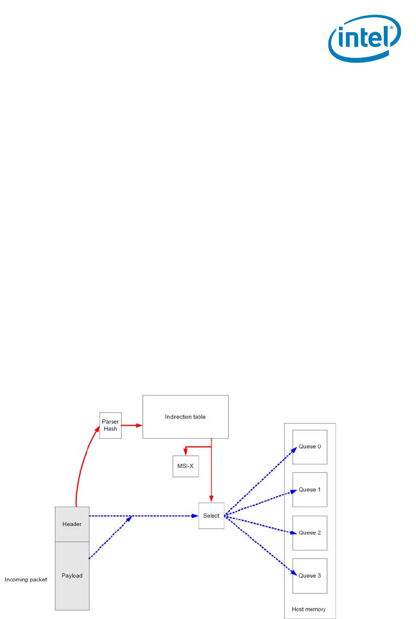
Multiple Receive Queues — Intel® 82575EB Gigabit Ethernet Controller
324632-003 Intel® 82575EB Gigabit Ethernet Controller
Revision: 2.1 Software Developer’s Manual and EEPROM Guide
January 2011 119
These registers hold a value that is an offset from the base and indicates the in-progress descriptor.
There can be up to 8 KB descriptors in the circular buffer. Hardware maintains a shadow copy that
includes those descriptors completed but not yet stored in memory.
• Receive Descriptor Tail registers (RDT0, RDT1, RDT2, RDT3)
These registers hold a value that is an offset from the base and identifies the location beyond the
last descriptor hardware can process. This is the location where software writes the first new
descriptor.
If software statically allocates buffers, and uses memory read to check for completed descriptors, it
simply has to zero the status byte in the descriptor to make it ready for re-use by hardware. This is not
a hardware requirement, but is necessary for performing an in-memory scan.
All the registers controlling the descriptor rings behavior should be set before receive is enabled, apart
from the tail registers which are used during the regular flow of data.
5.4 Multiple Receive Queues
The 82575 supports four receive descriptor Queues organized in ring structures. The ring functionality
is described in Section 5.3.8. The four receive queues are intended for use with the Receive Side
Scaling (RSS) algorithm. The following figure shows the implementation of multiple receive queues in
connection with RSS.
Note: For more information on manageability, refer to the 82575 TCO/System Manageability
Interface Application Note (AP-495).
Figure 4. Multiple Queues in Receive
First, the software application stores into the indirection table a set of values, enabling pre-determined
indirection of incoming packets to specific queues, each queue being dedicated to one processor. This
enables load balancing of multiple connections among the processors.

Intel® 82575EB Gigabit Ethernet Controller — Queuing for Virtual Machine Devices (VMDq)
Intel® 82575EB Gigabit Ethernet Controller 324632-003
Software Developer’s Manual and EEPROM Guide Revision: 2.1
120 January 2011
When receiving an incoming packet, its header is analyzed, according to the protocol used (IPv4, IPv6,
etc.). The connection-related fields are parsed and then a hash function is performed. The outcome of
the hash function is used to index into the indirection table memory; the value stored in this table is
used to generate an input to the Select modules that indicates to which queue the incoming packet is
going to be directed.
The number of processors in use need to fit the number of queues. As a result, when a platform
features more than four processors, only four of them are allocated to the Rx queues.
5.4.1 Queuing for Virtual Machine Devices (VMDq)
VMDs are I/O devices specifically targeted for sharing in a virtual system. In a virtual system, multiple
operating systems are loaded and each executes as though the entire system's resources are available
for each. However, for the limited number of I/O devices, this presents a problem because each
operating system might be in a separate memory domain and all the data movement and device
management has to be done by a VMM (Virtual Machine Monitor). VMM access adds latency and delay
to I/O accesses and degrades I/O performance. VMDs are designed to reduce the burden of VMM by
making certain functions of an I/O device shared and thus can be accessed directly from each guest
operating system or Virtual Machine (VM). The 82575's four queues can be accessed by four different
VMs if configured properly. When the 82575 is enabled for multiple queue direct access for VMs, it
becomes a VMDq device.
Note: Most configuration and resources are shared across queues. System software must resolve
any conflicts in configuration between the VMs.
The 82575 provides several options for sharing the four receive queues among VMs:
• VMs are associated with receive queues based on the packet destination MAC address
• VMs are associated with receive queues based on the packet VLAN tag ID
• VMs are associated with receive queues based on the packet destination MAC address and Receive
Side Scaling (RSS)
• VMs are associated with receive queues based on the packet VLAN tag ID and Receive Side Scaling
(RSS)
The appropriate mode is defined through the Multiple Receive Queues Enable field in the Multiple
Receive Queues Command register (MRQC). If promiscuous mode is enabled, packets that do not
match into a specific queue are routed into a default queue defined by the VMDq Control register
(VMD_CTL). Promiscuous mode is used to support more than four VMs so that the busier VMs are
assigned specific queues while all other VMs share the default queue. Unless assigned a dedicated MAC
address and a specific port, multicast and broadcast packets will be sent to the default queue.
Note: Packets must pass the regular receive filtering rules to be posted into any of the receive
queues.
5.4.1.1 Association Through MAC Address
Each of the 16 MAC address filters can be associated with one of the four receive queues. A packet that
matches a certain filter (and is eligible to be passed to the host) is routed to the respective queue. The
QSEL field in the Receive Address High register (RAH) determines the target queue. Packets that do not
match any of the MAC filters (broadcast, promiscuous, etc.) are forwarded to the default queue.

Queuing for Virtual Machine Devices (VMDq) — Intel® 82575EB Gigabit Ethernet Controller
324632-003 Intel® 82575EB Gigabit Ethernet Controller
Revision: 2.1 Software Developer’s Manual and EEPROM Guide
January 2011 121
Software can program different values to the MAC filters (any bits in RAH or RAL) at any time. The
82575 responds to the change on a packet boundary but does not guarantee the change to take place
at some precise time.
5.4.1.2 Association Through MAC Address + RSS
This mode combines classification through a MAC address and load balancing via RSS. MAC addressing
is used to classify packets to two pools (where a pool can be associated with a VM). RSS is then used
for each pool to determine the exact queue or processor. A single RSS Redirection Table serves both
pools; with the first half of each entry dedicated to pool 0 and the second half to pool 1. Note that the
same RSS key is used for both pools.
This scheme is targeted for VMDq use as well as future uses such as classification between a LAN pool
and an iSCSI pool.
This two-stage procedure operates as follows:
• The MSB of the QSEL field (QSEL[19]) in the Receive Address High register (RAH) matched by the
Destination Address determines the target pool.
• The index into the RSS Redirection Table is computed as in described in Section 5.4.2.
Software might program different values to the MAC filters (any bits in RAH or RAL) at any time. The
82575 responds to the change on a packet boundary but does not guarantee the change to take place
at some precise time.
Packets that do not match any of the MAC filters (broadcast, promiscuous, etc.) are forwarded to the
default pool and are further classified by the RSS rules for that queue.
A packet forwarded to a queue (either by MAC address matching or by default), that cannot receive an
RSS hash value is assigned to the default queue of this pool.
5.4.1.3 Association through VLAN tag ID
When MRCQ.MRQE = 100b, packets are forwarded to a queue according to their VLAN tag ID. The VLAN
tag of the packet is used as an index to a table that indicates the queue to which the packet should be
routed. The table is created by the VFQA1 (msb) and VFQA0 (lsb).
Note: Note: The VLAN tags that should be received should also be set in the VFTA table.
5.4.1.4 Association through VLAN tag ID +RSS
This mode combines classification through VLAN tag ID and load balancing via RSS. VLAN tag ID
filtering is used to classify packets to 2 pools (where a pool may be associated with a VM) using the
VFQA1 table. RSS is then used for each pool to determine the exact queue or processor. A single RSS
Redirection Table serves both pools; with the first half of each Indirection Table entry dedicated to pool
0 and the second half to pool 1.
The RSS redirection method is similar to the method used when associating queues by MAC address
+RSS.
Note: Note: The VLAN tags that should be received should also be set in the VFTA table

Intel® 82575EB Gigabit Ethernet Controller — Multiple Receive Queues & Receive-Side Scaling
(RSS)
Intel® 82575EB Gigabit Ethernet Controller 324632-003
Software Developer’s Manual and EEPROM Guide Revision: 2.1
122 January 2011
5.4.2 Multiple Receive Queues & Receive-Side Scaling
(RSS)
The 82575 provides four hardware receive queues and filters each receive packet into one of the
queues based on criteria described in the sections that follow. Classification of packets into receive
queues have several uses such as Receive Side Scaling (RSS), generic Multiple receive queues, or
Priority receive queues. However, RSS is the only usage that is described specifically. Other uses should
make use of the available hardware.
Multiple Receive Queues are enabled when the RXCSUM.PCSD bit is set (Packet Checksum is disabled)
and the Multiple Receive Queues Enable bits are not set to 00b. Multiple Receive Queues are therefore
mutually exclusive with UDP fragmentation. Also, support for multiple queues is not provided when
legacy receive descriptor format is used.
When Multiple Receive Queues are enabled, the 82575 provides software with several types of
information. Some are requirements of RSS while other are provided for device driver assistance:
• A Dword result of the RSS hash function. This is used by the stack for flow classification and is
written into the receive packet descriptor (required by RSS).
• A 4-bit RSS Type field. This conveys the hash function used for the specific packet (required by
RSS).
The following summarizes the process of classifying a packet into a receive queue:
1. The receive packet is parsed into the header fields used by the hash operation (for example, IP
addresses, TCP/UDP port, etc.)
2. A hash calculation is performed. The 82575 supports a single hash function as defined by RSS. The
82575 does not indicate to the device driver which hash function is used. The 32-bit result is fed
into the receive packet descriptor.
3. The seven LSBs of the hash result are used as an index into a 128-entry Redirection Table. Each
entry provides a 2-bit Queue number that indicates the queue into which the packet should be
routed.
When multiple receive queues are disabled, packets enter hardware queue 0. System software can
enable or disable RSS at any time. While disabled, system software can update the contents of any of
the RSS-related registers. While RSS is enabled, software can update the Indirection Table at any time.
When multiple request queues are enabled in RSS mode, un-decodable packets enter hardware queue
0. The 32-bit tag (normally a result of the hash function) equals 0b.
5.4.2.1 RSS Hash Function
A single hash function is defined with six variations for the following cases:
• IPv4. The 82575 parses the packet and uses the IPv4 source and destination addresses to generate
the hash value.
• TCP/IPv4. The 82575 parses the packet to identify an IPv4 packet containing a TCP segment. The
82575 uses the IPv4 source and destination addresses and the TCP local and remote port values to
generate the hash value.
• IPv6. The 82575 parses the packet to identify an IPv6 packet and uses the IPv6 source and
destination addresses to generate the hash value.
• TCP/IPv6. The 82575 parses the packet to identify an IPv6 packet containing a TCP segment. The
82575 uses the IPv6 source and destination addresses and the TCP local and remote port values to
generate the hash value.

Multiple Receive Queues & Receive-Side Scaling (RSS) — Intel® 82575EB Gigabit Ethernet
Controller
324632-003 Intel® 82575EB Gigabit Ethernet Controller
Revision: 2.1 Software Developer’s Manual and EEPROM Guide
January 2011 123
• IPv6Ex. The 82575 parses the packet to identify an IPv6 packet. Extension headers should be
parsed for a Home-Address-Option field (for source address) or the Routing-Header-Type-2 field
(for destination address). Note that the packet is not required to contain any of these extension
headers to be hashed by this function. If the specified extension headers are not present in the
packet, the 82575 uses the source/destination from the standard IPv6 header.
• TCPIPv6Ex. The 82575 parses the packet to identify an IPv6 packet containing a TCP segment with
extensions. Extension headers should be parsed for a Home-Address-Option field (for source
address) or the Routing-Header-Type-2 field (for destination address). Note that the packet is not
required to contain any of these extension headers to be hashed by this function. If the specified
extension headers are not present in the packet, the 82575 uses the source/destination from the
standard IPv6 header.
The following cases are in addition to the RSS standard:
• UDPIPv4 - The 82575 parses the packet to identify a packet with UDP over IPv4
• UDPIPv6 - The 82575 parses the packet to identify a packet with UDP over IPv6
• UDPIPv6Ex - The 82575 parses the packet to identify a packet with UDP over IPv6 with extensions
A packet is identified as containing a TCP segment if all of the following conditions are met:
• The transport layer protocol is TCP (not UDP, ICMP, IGMP, etc.).
• The TCP segment can be parsed (for example, IP options can be parsed or the packet is not
encrypted).
• The packet is not IP fragmented (even if the fragment contains a complete TCP header).
Note: When RSS is enabled (MRQC.MRQE equals 010b, 101b or 110b), TCP Rx checksum must
also be enabled (RXCSUM.TUOFL = 1b).
Bits[31:16] of the Multiple Receive Queues Command (MRQC) register enable each of the above hash
function variations (several may be set at a given time). If several functions are enabled at the same
time, priority is defined as follows (skip functions that are not enabled):
• IPv4 Packet.
a. Try using the TCP/IPv4 function.
b. Try using the IPv4_UDP function.
c. Try using the IPv4 function.
• IPv6 Packet.
a. If TCPIPv6Ex is enabled, try using the TCP/IPv6Ex function; else, if TCPIPv6 is enabled, try using
the TCPIPv6 function.
b. If UDPIPv6Ex is enabled, try using the UDPIPv6EX function; else, if UDPIPv6 is enabled, try using
the UDPIPv6 function.
c. If IPv6Ex is enabled, try using the IPv6Ex function; else, if IPv6 is enabled, try using the IPv6
function.
The following combinations are currently supported:
• Any combination of IPv4, TCPIPv4, and UDPIPv4, and or,
• Any combination of either IPv6, TCPIPv6, and UDPIPv6 or IPv6Ex, TCPiPv6Ex, and UDPIPv6Ex
When a packet cannot be parsed by the above rules, it enters hardware queue 0. The 32-bit tag (which
is a result of the hash function) equals 0. The 5-bit MRQ field also equals zero.
In the case of tunneling (for example, IPv4-IPv6 tunnel), the external IP address (in the base header)
is used.

Intel® 82575EB Gigabit Ethernet Controller — Multiple Receive Queues & Receive-Side Scaling
(RSS)
Intel® 82575EB Gigabit Ethernet Controller 324632-003
Software Developer’s Manual and EEPROM Guide Revision: 2.1
124 January 2011
The 32-bit result of the hash computation is written into the packet descriptor and also provides an
index into the Indirection Table.
The following notation is used to describe the following hash functions:
• Ordering is little endian in both bytes and bits. For example, the IP address 161.142.100.80
translates into A18E 6450h in the signature.
• A “^” denotes bit-wise eXclusive OR (XOR) operation of same width vectors.
• @x-y denotes bytes x through y (including both of them) of the incoming packet, where byte 0 is
the first byte of the IP header. In other words, we consider all byte offsets as offsets into a packet
where the framing layer header has been stripped out. Therefore, the source IPv4 address is
referred to as @12-15, while the destination v4 address is referred to as @16-19.
• @x-y, @v-w denotes concatenation of bytes x-y followed by bytes v-w, preserving the order in
which they occurred in the packet.
All hash function variations (IPv4 and IPv6) follow the same general structure. Specific details for each
variation are described in the following section. The hash uses a random secret key of length 320 bits
(40 bytes). The key is generated and supplied through the RSS Random Key Register (RSSRK).
The algorithm works by examining each bit of the hash input from left to right. Our nomenclature
defines left and right for a byte array as follows:
Given an array K with k bytes, our nomenclature assumes that the array is laid out as:
K[0] K[1] K[2] … K[k-1]
K[0] is the left most byte, and the most significant bit of K[0] is the left most bit. K[k-1] is the right
most byte, and the least significant bit of K[k-1] is the right most bit.
ComputeHash(input[], N)
For hash-input input[] of length N bytes (8N bits) and a random secret key K of 320 bits
Result = 0;
For each bit b in input[] {
if (b == 1) then Result ^= (left-most 32 bits of K);
shift K left 1 bit position;
}
return Result;
The following four pseudo-code examples are intended to help clarify exactly how the hash is to be
performed in four cases: IPv4 with and without ability to parse the TCP header and IPv6 with and
without a TCP header.
5.4.2.1.1 Hash for IPv4 with TCP
Concatenate SourceAddress, DestinationAddress, SourcePort, DestinationPort into one
single byte-array, preserving the order in which they occurred in the packet: Input[12]
= @12-15, @16-19, @20-21, @22-23.
Result = ComputeHash(Input, 12);

Multiple Receive Queues & Receive-Side Scaling (RSS) — Intel® 82575EB Gigabit Ethernet
Controller
324632-003 Intel® 82575EB Gigabit Ethernet Controller
Revision: 2.1 Software Developer’s Manual and EEPROM Guide
January 2011 125
5.4.2.1.2 Hash for IPv4 with UDP
Concatenate SourceAddress, DestinationAddress, SourcePort, DestinationPort into one
single byte-array, preserving the order in which they occurred in the packet: Input[12]
= @12-15, @16-19, @20-21, @22-23.
Result = ComputeHash(Input, 12);
5.4.2.1.3 Hash for IPv4 without TCP
Concatenate SourceAddress and DestinationAddress into one single byte-array
Input[8] = @12-15, @16-19
Result = ComputeHash(Input, 8)
5.4.2.1.4 Hash for IPv6 with TCP
Similar to above:
Input[36] = @8-23, @24-39, @40-41, @42-43
Result = ComputeHash(Input, 36)
5.4.2.1.5 Hash for IPv6 with UDP
Similar to above:
Input[36] = @8-23, @24-39, @40-41, @42-43
Result = ComputeHash(Input, 36)
5.4.2.1.6 Hash for IPv6 without TCP
Input[32] = @8-23, @24-39
Result = ComputeHash(Input, 32)
5.4.2.2 Indirection Table
The indirection table is a 128-entry structure, indexed by the 7 least significant bits of the hash function
output. Each entry of the table contains the following:
• Bit [7:6]: Queue index. for pool 1 or regular RSS
• Bits [5:4]: Reserved
• Bits [3:2]: Queue index for pool 0
• Bits [1:0]: Reserved
The Queue Index determines the physical queue for the packet.
System software can update the indirection table during run time. Such updates of the table are not
synchronized with the arrival time of received packets. Therefore, it is not guaranteed that a table
update takes effect on a specific packet boundary.

Intel® 82575EB Gigabit Ethernet Controller — RSS Verification Suite
Intel® 82575EB Gigabit Ethernet Controller 324632-003
Software Developer’s Manual and EEPROM Guide Revision: 2.1
126 January 2011
5.4.2.3 Support for Multiple Processors
It is assumed that each queue is associated with a specific processor, even when there are more
processors than queues.
5.4.3 RSS Verification Suite
This section contains the values used in the given examples. Assume that the random key byte-stream
is:
0x6d, 0x5a, 0x56, 0xda, 0x25, 0x5b, 0x0e, 0xc2,
0x41, 0x67, 0x25, 0x3d, 0x43, 0xa3, 0x8f, 0xb0,
0xd0, 0xca, 0x2b, 0xcb, 0xae, 0x7b, 0x30, 0xb4,
0x77, 0xcb, 0x2d, 0xa3, 0x80, 0x30, 0xf2, 0x0c,
0x6a, 0x42, 0xb7, 0x3b, 0xbe, 0xac, 0x01, 0xfa
5.4.3.1 IPv4
5.4.3.2 IPv6
The IPv6 address tuples are only for verification purposes and may not make sense as a tuple.
Destination Address/
Port Source Address/Port IPv4 only IPv4 with TCP
161.142.100.80 :1766 66.9.149.187 :2794 323E 8FC2h 51CC C178h
65.69.140.83 :4739 199.92.111.2 :14230 D718 262Ah C626 B0EAh
12.22.207.184 :38024 24.19.198.95 :12898 D2D0 A5DEh 5C2B 394Ah
209.142.163.6 :2217 38.27.205.30 :48228 8298 9176h AFC7 327Fh
202.188.127.2 :1303 153.39.163.191 :44251 5D18 09C5h 10E8 28A2h
Destination Address/Port Source Address/Port IPv6 only IPv6 with TCP
3FFE:2501:200:1FFF::7
(1766)
3FFE:2501:200:3::1
(2794)
2CC1 8CD5 4020 7D3D
FF02::1
(4739)
3FFE:501:8::260:97FF:FE40:EF
AB
(14230)
0F0C 461C DDE5 1BBF
FE80::200:F8FF:FE21:67CF
(38024)
3FFE:1900:4545:3:200:F8FF:F
E21:67CF
(44251)
4B61 E985 02D1 FEEF
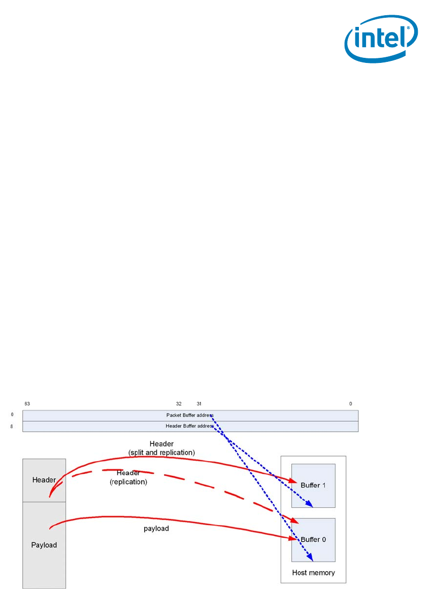
Header Splitting and Replication — Intel® 82575EB Gigabit Ethernet Controller
324632-003 Intel® 82575EB Gigabit Ethernet Controller
Revision: 2.1 Software Developer’s Manual and EEPROM Guide
January 2011 127
5.5 Header Splitting and Replication
This feature consists of splitting or replicating a packet’s header to a different memory space. This helps
the host to fetch headers only for processing: headers are replicated through a regular snoop
transaction, in order to be processed by the host processor. It is recommended to perform this
transaction with the DCA feature enabled.
The packet (header + payload) is stored in memory through an optional non-snoop transaction.
The 82575 supports header splitting in several modes:
• Legacy mode: legacy descriptors are used; headers and payloads are not split.
• Advanced mode, no split: advanced descriptors are in use; header and payload are not split.
• Advanced mode, split: Advanced descriptors are in use; header and payload are split to different
buffers.
• Advanced mode, replication: Advanced descriptors are in use; header is replicated in a separate
buffer and in a payload buffe.r
• Advanced mode, replication, conditioned by packet size: Advanced descriptors are in use;
replication is performed only if the packet is larger than the header buffer size.
• Advanced mode, split: always use header buffer: Advanced descriptors are in use; header and
payload are split to different buffers. If no split is done, the first part of the packet is stored in the
header buffer.
Header splitting and header replication modes are shown in Figure 5.
Figure 5. Header Splitting with Replicated Header
The physical address of each buffer is written in the Buffer Addresses fields. The sizes of these buffers
are statically defined by BSIZEPACKET in the SRRCTL[n] registers.
The Packet Buffer Address includes the address of the buffer assigned to the replicated packet,
including header and data payload portions of the received packet. In case of split header, only the
payload is included.

Intel® 82575EB Gigabit Ethernet Controller — Header Splitting and Replication
Intel® 82575EB Gigabit Ethernet Controller 324632-003
Software Developer’s Manual and EEPROM Guide Revision: 2.1
128 January 2011
The Header Buffer Address includes the address of the buffer that contains the header information. The
Receive DMA module stores the header portion of the received packets into this buffer.
The 82575 uses the Packet Replication or splitting feature when the SRRCTL[n].DESCTYPE is greater
than one. The software device driver must also program the buffer sizes in the SRRCTL[n] registers.
When Header split is selected, the packet is split only on selected types of packets. A bit exists for each
option in PSRTYPE[n] registers, so several options can be used in conjunction. If one or more bits are
set, the splitting is performed for the corresponding packet type.
Table 33 lists the behavior of the 82575 in the different modes.

Header Splitting and Replication — Intel® 82575EB Gigabit Ethernet Controller
324632-003 Intel® 82575EB Gigabit Ethernet Controller
Revision: 2.1 Software Developer’s Manual and EEPROM Guide
January 2011 129
Table 33. Header Splitting and Header Replication Mode
Note: If SRRCTL#.NSE is set, all buffers' addresses in a packet descriptor must be word aligned.
The packet header cannot span across buffers, therefore, the size of the header buffer must
be larger than any expected header size. Otherwise, only the part of the header fitting the
header buffer is replicated. In case of header split mode (SRRCTL.DESCTYPE = 010b), a
packet with a header larger than the header buffer will not be split.
DESCTYPE Condition SPH HBO PKT LEN HDR LEN Copy
Split Header cannot be
decoded
0b 0b Min(packet
length buffer
size
N/A Header + Payload Packet
Buffer
Header <=
BSIZEHEADER
1b 0b Min(payload
length buffer
size1
1. In a header only packet (for example. TCP ACK packet), PKT_LEN is 0b.
Header
size
Header Packet Buffer
Payload Packet Buffer
Header > BSIZEHEADER 1b 1b Min(packet
length buffer
size
Header
size2
2. The HDR_LEN doesn't reflect the actual data size stored in the header buffer. It reflects the header size determined by the parser.
Header + Payload Packet
Buffer
Split (always
use header
buffer
Packet length <=
BSIZEHEADER
0b 0b 0b Packet
length
Header + Payload Header
Buffer
Header cannot be
decoded (packet length
> BSIZEHEADER)
0b 0b Min(packet
length -
BSIZE-
HEADER, data
buffer size)
BSIZE-
HEADER
Header + Payload Header +
Packet Buffer3
3. If the packet spans more than one descriptor, only the header buffer of the first descriptor is used.
Header <=
BSIZEHEADER
1b 0b Min(payload
length, data
buffer size)
Header
size
Header Header Buffer
Payload Packet Buffer
Header > BSIZEHEADER 1b 1b Min(packet
length -
BSiZE-
HEADER, data
buffer size)
Header
sizebHeader + Payload Header +
Packet Buffer
Replicate Header + payload <=
BSIZEHEADER
0b/
1b
0b Min(packet
length, buffer
size
Header
size,
N/A4
4. If SPH = 0b, then the header size is not relevant. In any case, the HDR_LEN doesn't reflect the actual data size stored in the Header
buffer.
Header + Payload Header
Buffer
Header + Payload Packet
Buffer
Header + Payload >
BSIZEHEADER
0b/
1b
0b/1b5
5. HBO is 1b if the header size is bigger than BSIZEHEADER; otherwise, 0b.
Min(packet
length, buffer
size)
Header
size,
N/Ad
(Header + Payload)(partialf)
Header Buffer
Header + Payload Packet
Buffer
Replicate large
packet
Header + payload <=
BSIZEHEADER
0b/
1b
0b Packet length Header
size,
N/Ad
Header + Payload Header
Buffer
Header + Payload >
BSIZEHEADER
0b/
1b
0b/1beMin(packet
length, buffer
size)
Header
size,
N/Ad
(Header + Payload)(partial6)
Header Buffer
Header + Payload Packet
Buffer
6. Partial means up to BSIZEHEADER.

Intel® 82575EB Gigabit Ethernet Controller — Receive Packet Checksum Offloading
Intel® 82575EB Gigabit Ethernet Controller 324632-003
Software Developer’s Manual and EEPROM Guide Revision: 2.1
130 January 2011
5.5.1 Receive Packet Checksum Offloading
The 82575 supports the offloading of three receive checksum calculations: the Packet Checksum, the
IPv4 Header Checksum, and the TCP/UDP Checksum.
The Packet checksum is the one's complement over the receive packet, starting from the byte indicated
by RXCSUM.PCSS (0b corresponds to the first byte of the packet), after stripping. For packets with
VLAN header, the packet checksum includes the header if VLAN striping is not enabled by the
CTRL.VME. If VLAN header strip is enabled, the packet checksum and the starting offset of the packet
checksum exclude the VLAN header due to masking of VLAN header. For example, for an Ethernet II
frame encapsulated as an 802.3ac VLAN packet and CTRL.VME is set and with RXCSUM.PCSS set to 14,
the Packet Checksum includes the entire encapsulated frame, excluding the 14-byte Ethernet header
(DA, SA, Type/Length) and the 4-byte q-tag. The packet checksum does not include the Ethernet CRC if
the RCTL.SECRC bit is set.
Software must make the required offsetting computation (to back out the bytes that should not have
been included and to include the pseudo-header) prior to comparing the Packet Checksum against the
TCP checksum stored in the packet.
For supported packet/frame types, the entire checksum calculation can be off-loaded to the 82575. If
RXCSUM.IPOFL is set to 1b, the 82575 calculates the IPv4 checksum and indicates a pass/fail indication
to software via the IPv4 Checksum Error bit (RDESC.IPE) in the ERROR field of the receive descriptor.
Similarly, if RXCSUM.TUOFL is set to 1b, the 82575 calculates the TCP or UDP checksum and indicates a
pass/fail condition to software via the TCP/UDP Checksum Error bit (RDESC.TCPE). These error bits are
valid when the respective status bits indicate the checksum was calculated for the packet (RDESC.IPCS
and RDESC.TCPCS respectively). Similarly, if RFCTL.IPv6_DIS and RFCTL.IP6Xsum_DIS are cleared to
0b and RXCSUM.TUOFL is set to 1b, the 82575 calculates the TCP or UDP checksum for IPv6 packets. It
then indicates a pass/fail condition in the TCP/UDP Checksum Error bit (RDESC.TCPE).
If neither RXCSUM.IPOFLD nor RXCSUM.TUOFLD is set, the Checksum Error bits (IPE and TCPE) is 0b
for all packets.
Supported Frame Types include:
• Ethernet II
• Ethernet SNAP
Table 34. Supported Receive Checksum Capabilities
Packet Type HW IP Checksum Calculation HW TCP/UDP Checksum Calculation
IPv4 packets Yes1Yes
IPv6 packets No (n/a) Yes
IPv6 packet with next header options:
• Hop-by-Hop options
• Destinations options
• Routing (with LEN 0)
• Routing (with LEN > 0
• Fragment
• Home option
No (n/a)
No (n/a)
No (n/a)
No (n/a)
No (n/a)
No (n/a)
Yes
Yes
Yes
No
No
No
IPv4 tunnels:
• IPv4 packet in an IPv4 tunnel
• IPv6 packet in an IPv4 tunnel
Either IP or TCPa
Either IP or TCPa
Either IP or TCPa
Either IP or TCPa

Receive Packet Checksum Offloading — Intel® 82575EB Gigabit Ethernet Controller
324632-003 Intel® 82575EB Gigabit Ethernet Controller
Revision: 2.1 Software Developer’s Manual and EEPROM Guide
January 2011 131
Table 34 lists the general details about what packets are processed. In more detail, the packets are
passed through a series of filters to determine if a receive checksum is calculated.
5.5.1.1 MAC Address Filter
This filter checks the MAC destination address to be sure it is valid (IA match, broadcast, multicast,
etc.). The receive configuration settings determine which MAC addresses are accepted. See the various
receive control configuration registers such as RCTL (RTCL.UPE, RCTL.MPE, RCTL.BAM), MTA, RAL, and
RAH.
5.5.1.2 SNAP/VLAN Filter
This filter checks the next headers looking for an IP header. It is capable of decoding Ethernet II,
Ethernet SNAP, and IEEE 802.3ac headers. It skips past any of these intermediate headers and looks
for the IP header. The receive configuration settings determine which next headers are accepted. See
the various receive control configuration registers such as RCTL (RCTL.VFE), VET, and VFTA.
5.5.1.3 IPv4 Filter
This filter checks for valid IPv4 headers. The version field is checked for a correct value (4). IPv4
headers are accepted if they are any size greater than or equal to 5 (Dwords). If the IPv4 header is
properly decoded, the IP checksum is checked for validity. The RXCSUM.IPOFL bit must be set for this
filter to pass.
5.5.1.4 IPv6 Filter
This filter checks for valid IPv6 headers, which are a fixed size and have no checksum. The IPv6
extension headers accepted are: Hop-by-Hop, Destination Options, and Routing. The maximum size
next header accepted is 16 Dwords (64 bytes).
IPv6 tunnels:
• IPv4 packet in an IPv6 tunnel
• IPv6 packet in an IPv6 tunnel
No
No
No
No
Packet is an IPv4 fragment Yes No
Packet is greater than 1552 bytes; (LPE=1b) Yes Yes
Packet has 802.3ac tag Yes Yes
IPv4 Packet has IP options
(IP header is longer than 20 bytes)
Yes Yes
Packet has TCP or UDP options Yes Yes
IP header’s protocol field contains a protocol #
other than TCP or UDP.
Yes No
1. For tunnels, the software device driver might only do the TCP checksum or Ipv4 checksum. If the TCP checksum is desired, the
software device driver should define the IP header length as the combined length of both IP headers in the packet. If an IPv4
checksum is required, the IP header length should be set to the Ipv4 header length.
Table 34. Supported Receive Checksum Capabilities
Packet Type HW IP Checksum Calculation HW TCP/UDP Checksum Calculation

Intel® 82575EB Gigabit Ethernet Controller — Receive Packet Checksum Offloading
Intel® 82575EB Gigabit Ethernet Controller 324632-003
Software Developer’s Manual and EEPROM Guide Revision: 2.1
132 January 2011
5.5.1.5 IPv6 Extension Headers
IPv4 and TCP provide header lengths that allow hardware to easily navigate through these headers on
packet reception for calculating checksums and CRCs, etc. For receiving IPv6 packets, however, there is
no IP header length to help hardware find the packet's ULP (such as TCP or UDP) header. One or more
IPv6 extension headers might exist in a packet between the basic IPv6 header and the ULP header.
Hardware must skip over these extension headers to calculate the TCP or UDP checksum for received
packets.
The IPv6 header length without extensions is 40 bytes. The IPv6 field Next Header Type indicates what
type of header follows the IPv6 header at offset 40. It might be an upper layer protocol header such as
TCP or UDP (Next Header Type of 6 or 17, respectively), or it might indicate that an extension header
follows. The final extension header indicates with its Next Header Type field the type of ULP header for
the packet.
IPv6 extension headers have a specified order. However, destinations must be able to process these
headers in any order. Also, IPv6 (or IPv4) can be tunneled using IPv6, and thus another IPv6 (or IPv4)
header and potentially its extension headers can be found after the extension headers.
The IPv4 Next Header Type is at byte offset 9. In IPv6, the first Next Header Type is at byte offset 6.
All IPv6 extension headers have the Next Header Type in their first 8 bits. Most have the length in the
second 8 bits (Offset Byte[1]) as shown:
Table 35 lists the encodings of the Next Header Type field and information on determining each header
type's length. The IPv6 extension headers are not otherwise processed by the 82575 so details are not
covered.
123
0 1 2 3 4 5 6 7 8 9 0 1 2 3 4 5 6 7 8 9 0 1 2 3 4 5 6 7 8 9 0 1
Next Header Type Length

Packet Transmission — Intel® 82575EB Gigabit Ethernet Controller
324632-003 Intel® 82575EB Gigabit Ethernet Controller
Revision: 2.1 Software Developer’s Manual and EEPROM Guide
January 2011 133
Table 35. Next Header Type Encodings
Note: The 82575 hardware acceleration does not support all IPv6 Extension header types. Also,
the RFCTL.Ipv6_DIS bit must be cleared for this filter to pass.
5.5.1.6 UDP/TCP Filter
This filter checks for a valid UDP or TCP header. The prototype next header values are 11h and 06h,
respectively. The RXCSUM.TUOFL bit must be set for this filter to pass.
5.6 Packet Transmission
The transmission process for regular (non-TCP Segmentation packets) involves:
• The protocol stack receives from an application a block of data that is to be transmitted.
• The protocol stack calculates the number of packets required to transmit this block based on the
MTU size of the media and required packet headers.
• For each packet of the data block:
— Ethernet, IP and TCP/UDP headers are prepared by the stack.
— The stack interfaces with the software device driver and commands the driver to send the
individual packet.
— The software device driver gets the frame and interfaces with the hardware.
— The hardware reads the packet from host memory (via DMA transfers).
— The driver returns ownership of the packet to the Network Operating System (NOS) when the
hardware has completed the DMA transfer of the frame (indicated by an interrupt).
Header Next Header Type Header Length
(units are in bytes unless otherwise
specified)
IPv6 6 Always 40 bytes
IPv4 4 Offset bits [7:4]
Unit = 4 bytes
TCP 6 Offset byte [12, bits [7:4]]
Unit = 4 bytes
UDP 17 Always 8 bytes
Hop by Hop Options 01
1. Hop by Hop Options Header is only found in the first Next Header Type of an IPv6 Header.
8 + offset byte [1]
Destination Options 60 8 + offset byte [1]
Routing 43 8 + offset byte [1]
Fragment 44 Always 8 bytes
Authentication 51 8 + 4* (offset byte [1])
Encapsulating Security Payload 50 2
2. Encapsulated Security Payload.
No Next Header 59 3
3. When a No Next Header type is encountered, the rest of the packet should not be processed.

Intel® 82575EB Gigabit Ethernet Controller — Transmit Data Storage
Intel® 82575EB Gigabit Ethernet Controller 324632-003
Software Developer’s Manual and EEPROM Guide Revision: 2.1
134 January 2011
Output packets are made up of pointer–length pairs constituting a descriptor chain (so called descriptor
based transmission). Software forms transmit packets by assembling the list of pointer–length pairs,
storing this information in the transmit descriptor, and then updating the on–chip transmit tail pointer
to the descriptor. The transmit descriptor and buffers are stored in host memory. Hardware typically
transmits the packet only after it has completely fetched all packet data from host memory and
deposited it into the on-chip transmit FIFO. This permits TCP or UDP checksum computation, and avoids
problems with PCIe* underruns.
Another transmit feature is TCP Segmentation. The hardware has the capability to perform packet
segmentation on large data buffers off-loaded from the Network Operating System (NOS). This feature
is described in detail in Section 5.8.
5.6.1 Transmit Data Storage
Data are stored in buffers pointed to by the descriptors. Alignment of data is on an arbitrary byte
boundary with the maximum size per descriptor limited only to the maximum allowed packet size (9018
bytes). A packet typically consists of two (or more) descriptors, one (or more) for the header and one
for the actual data. Some software implementations copy the header(s) and packet data into one buffer
and use only one descriptor per transmitted packet.
5.6.2 Transmit Contexts
The 82575 provides hardware checksum offload and TCP Segmentation facilities. These features enable
TCP and UDP packet types to be handled more efficiently by performing additional work in hardware,
thus reducing the software overhead associated with preparing these packets for transmission. Part of
the parameters used by these features are handled though contexts.
A context refers to a set of device registers loaded or accessed as a group to provide a particular
function. The 82575 supports 16 context register sets on-chip. The transmit queues can contain
Transmit Data Descriptors, much like the receive queue, and also Transmit Context Descriptors.
A transmit context descriptor differs from a data descriptor as it does not point to packet data. Instead,
this descriptor provides the ability to write to the on-chip contexts that support the transmit checksum
offloading and the segmentation features of the 82575.
The 82575 supports one type of transmit context: the extended context is written with a Transmit
Context Descriptor DTYP = 2 and this context is always used for Transmit Data Descriptor DTYP = 3.
The IDX field contains an index to one of 16 on-chip contexts. Software must track what context is
stored in each IDX location. Also, each advanced descriptor must refer to a context unless no offload is
needed.
Contexts can be initialized with a Transmit Context Descriptor and then used for a series of related
Transmit Data Descriptors. The context, for example, defines the checksum and offload capabilities for
a given type of TCP/IP flows. All packets of this type can be sent using this context.
Contexts should only be over written by a Transmit Context Descriptor when there are no Transmit Data
Descriptors in any queue that point to it. This is the only way for software to ensure that the correct
context is used for the data. If context are statically allocated to queues and there are no cross
referencing between data descriptor from one queue and context descriptor of another queue, then
there are no limitation on the context descriptor setting.

Transmit Descriptors — Intel® 82575EB Gigabit Ethernet Controller
324632-003 Intel® 82575EB Gigabit Ethernet Controller
Revision: 2.1 Software Developer’s Manual and EEPROM Guide
January 2011 135
Each context defines information about the packet sent including the total size of the MAC header
(TDESC.MACHDR), the amount of payload data that should be included in each packet (TDESC.MSS),
TCP Header length (TDES.TCPHDR), IP Header length (TDESC.IPHDR) and information about what type
of protocol (TCP, IP, etc.) is used. Other than TCP, IP (TDESC.TUCMD), most information is specific to
the segmentation capability and is therefore ignored for context descriptors that do not have the TSE
bit set.
Because there are dedicated resources on-chip for contexts, they remain constant until they are
modified by another context descriptor. This means that a context can (and will) be used for multiple
packets (or multiple segmentation blocks) unless a new context is loaded prior to each new packet.
Depending on the environment, it might be completely unnecessary to load a new context for each
packet. For example, if most traffic generated from a given node is standard TCP frames, this context
could be setup once and used for many frames. Only when some other frame type is required would a
new context need to be loaded by software using a different index.
This same logic can also be applied to the segmentation context, though the environment is a more
restrictive one. In this scenario, the host is commonly asked to send messages of the same type, TCP/
IP for instance, and these messages also have the same Maximum Segment Size (MSS). In this
instance, the same segmentation context could be used for multiple TCP messages that require
hardware segmentation.
5.6.3 Transmit Descriptors
The 82575 supports legacy and advanced descriptors.
Legacy descriptors are intended to support legacy drivers, in order to allow fast power up of platform,
and to facilitate debug. The legacy descriptors are recognized as such based on the DEXT bit.
In addition, the 82575 supports two types of advanced transmit descriptors:
1. Advanced Transmit Context descriptor, DTYP = 0010b.
2. Advanced Transmit Data descriptor, DTYP = 0011b.
Note: DTYP = 0000b and 0001b are reserved values.
The Transmit Data Descriptor points to a block of packet data to be transmitted. The TCP/IP
Context Transmit Descriptor does not point to packet data. It contains control/context
information that is loaded into on-chip registers that affect the processing of packets for
transmission. The following sections describe the descriptor formats.
5.6.4 Legacy Transmit Descriptor Format
To select legacy mode operation, bit 29 of the second line of the descriptor (TDSEC.DEXT) should be set
to 0b. In this case, the descriptor format is defined as shown in Table 36. The address and length must
be supplied by software. Bits in the command byte are optional, as are the Checksum Offset (CSO), and
Checksum Start (CSS) fields.

Intel® 82575EB Gigabit Ethernet Controller — Transmit Descriptor Write Back Format
Intel® 82575EB Gigabit Ethernet Controller 324632-003
Software Developer’s Manual and EEPROM Guide Revision: 2.1
136 January 2011
Table 36. Transmit Descriptor (TDESC) Layout – Legacy Mode
5.6.5 Transmit Descriptor Write Back Format
5.6.5.1 Length
Length (TDESC.LENGTH) specifies the length in bytes to be fetched from the buffer address provided.
The maximum length associated with any single legacy descriptor is 9018 bytes.
Note: The maximum allowable packet size for transmits changes based on the value written to the
Packet Buffer Allocation register.
Descriptor length(s) can be limited by the size of the transmit FIFO. All buffers comprising a single
packet must be able to be stored simultaneously in the transmit FIFO. For any individual packet, the
sum of the individual descriptors' lengths must be below 9018 bytes.
Note: Descriptors with zero length (null descriptors) transfer no data. Null descriptors might
appear only between packets and must have their EOP bits set.
5.6.5.2 Checksum Offset and Start (CSO and CSS)
A checksum offset (TDESC.CSO) field indicates where, relative to the start of the packet, to insert a TCP
checksum if this mode is enabled. A checksum start (TDESC.CSS) field indicates where to begin
computing the checksum. Both CSO and CSS are in units of bytes. These must both be in the range of
data provided to the device in the descriptor. This means for short packets that are padded by software,
CSS and CSO must be in the range of the unpadded data length, not the eventual padded length (64
bytes).
With an 802.1Q header, the offset values depend on the VLAN insertion enable bit - CTRL.VME and the
VLE bit. If they are not set (VLAN tagging included in the packet buffers), the offset values should
include the VLAN tagging. If these bits are set (VLAN tagging is taken from the packet descriptor), the
offset values should exclude the VLAN tagging.
Hardware does not add the 802.1Q Ether Type or the VLAN field following the 802.1Q Ether Type to the
checksum. So for VLAN packets, software can compute the values to back out only on the encapsulated
packet rather than on the added fields.
Note: UDP checksum calculation is not supported by the legacy descriptor because the legacy
descriptor does not support the translation of a checksum result of 0000h to FFFFh needed
to differentiate between an UDP packet with a checksum of zero and an UDP packet without
checksum.
63 48 47 40 39 36 35 32 31 24 23 16 15 0
0 Buffer Address [63:0]
8 Special CSS ExtCMD STA CMD CSO Length
63 48 47 40 39 36 35 32 31 24 23 16 15 0
0 Buffer Address [63:0]
8 Special CSS Reserved STA CMD CSO Length

Transmit Descriptor Write Back Format — Intel® 82575EB Gigabit Ethernet Controller
324632-003 Intel® 82575EB Gigabit Ethernet Controller
Revision: 2.1 Software Developer’s Manual and EEPROM Guide
January 2011 137
Because the CSO field is eight bits wide, it puts a limit the location of the checksum to 255 bytes from
the beginning of the packet.
EOP, when set, indicates the last descriptor making up the packet. One or many descriptors can be used
to form a packet. Hardware inserts a checksum at the offset indicated by the CSO field if the Insert
Checksum bit (IC) is set. Checksum calculations are for the entire packet starting at the byte indicated
by the CSS field. A value of 0 corresponds to the first byte in the packet. CSS must be set in the first
descriptor for a packet. In addition, IC is ignored if CSO or CSS are out of range. This occurs if (CSS
length) or (CSO length - 1).
Note: CSO must be larger than CSS and CSS must be equal or bigger than 14 bytes, and CSO
must be smaller than the packet length minus 4 bytes.
5.6.5.3 Command Byte (CMD)
The CMD byte stores the applicable command and has fields shown in Table 37.
Software must compute an offsetting entry to back out the bytes of the header that are not part of the
IP pseudo header and should not be included in the TCP checksum and store it in the position where the
hardware computed checksum is inserted.

Intel® 82575EB Gigabit Ethernet Controller — Transmit Descriptor Write Back Format
Intel® 82575EB Gigabit Ethernet Controller 324632-003
Software Developer’s Manual and EEPROM Guide Revision: 2.1
138 January 2011
Table 37. Transmit Command (TDESC.CMD) Layout
Note: When tail write-back is enabled, the descriptor write-back is not executed.
7 6 5 4 3 2 1 0
RSV VLE DEXT RSV RS IC IFCS EOP
TDESC.CMD Description
Reserved (bit 7) Reserved.
VLE (bit 6) VLAN Packet Enable
Indicates that the packet is a VLAN packet (for example, hardware should add the VLAN Ether type and an
802.1q VLAN tag to the packet).
When set to 0b, sends generic Ethernet packet.
When set to 1b, sends 802.1Q packet; the Ethernet Type field comes from the VET register and the VLAN
data comes from the special field of the TX descriptor.
Note: If the VLE bit is set, the CTRL.VME bit should also be set to enable VLAN tag insertion. If the
CTRL.VME bit is not set, the 82575 does not insert VLAN tags on outgoing packets.
DEXT (bit 5) Extension (0b for legacy mode).
Should be written with 0b for future compatibility.
RSV (bit 4) Reserved
Should be programmed to 0b.
RS (bit 3) Report Status
Signals hardware to report the status information. This is used by software that does in-memory checks of
the transmit descriptors to determine which ones are done. For example, if software queues up 10 packets
to transmit, it can set the RS bit in the last descriptor of the last packet. If software maintains a list of
descriptors with the RS bit set, it can look at them to determine if all packets up to (and including) the one
with the RS bit set have been buffered in the output FIFO. Looking at the status byte and checking the
Descriptor Done (DD) bit do this. If DD is set, the descriptor has been processed.
IC (bit 2) Insert Checksum
When set, the 82575 needs to insert a checksum at the offset indicated by the CSO field. The checksum
calculations are performed for the entire packet starting at the byte indicated by the CCS field. IC is ignored
if CSO and CCS are out of the packet range. This occurs when (CSS length) or (CSO length - 1). IC is
valid only when EOP is set.
IFCS (bit 1) Insert FCS
When set, hardware appends the MAC FCS at the end of the packet. When cleared, software should
calculate the FCS for proper CRC check. There are several cases in which software must set IFCS:
Transmission of short packet while padding is enabled by the TCTL.PSP bit
Checksum offload is enabled by the IC bit in the TDESC.CMD
VLAN header insertion enabled by the VLE bit in the TDESC.CMD
EOP (bit 0) End Of Packet
When set, indicates the last descriptor making up the packet. One or many descriptors can be used to form
a packet.

Transmit Descriptor Special Field Format — Intel® 82575EB Gigabit Ethernet Controller
324632-003 Intel® 82575EB Gigabit Ethernet Controller
Revision: 2.1 Software Developer’s Manual and EEPROM Guide
January 2011 139
5.6.5.4 Transmit Descriptor Status Field Format
Table 38. Transmit Status Layout
5.6.6 Transmit Descriptor Special Field Format
The Special field is used to provide the 802.1q/802.1ac tagging information and is qualified only on the
first descriptor of each packet when the VLE bit is set.
3 2 1 0
Reserved DD
TDESC.STATUS Description
RSV (bits 3:1) Reserved.
Should be programmed to 000b.
DD (bit 0) Descriptor Done
Indicates that the descriptor is finished and is written back either after the descriptor has been processed
(with RS set).

Intel® 82575EB Gigabit Ethernet Controller — Advanced Transmit Context Descriptor
Intel® 82575EB Gigabit Ethernet Controller 324632-003
Software Developer’s Manual and EEPROM Guide Revision: 2.1
140 January 2011
Table 39. Special Field (TDESC.SPECIAL) Layout
5.6.7 Advanced Transmit Context Descriptor
Table 40. Transmit Context Descriptor (TDESC) Layout – (Type = 0010b)
Table 41. Transmit Context Descriptor (TDESC) Layout
15 13 12 11 0
PRI CFI VLAN
TDESC.SPECIAL Description
PRI User Priority
3 bits that provide the VLAN user priority field to be inserted in the 802.1Q tag.
CFI Canonical Form Indicator.
VLAN VLAN Identifier
12 bits that provide the VLAN identifier field to be inserted in the 802.1Q tag.
63 48 47 40 39 32 31 1
615 9 8 0
0 SN VLAN MACLEN IPLEN
8 MSS L4LEN IDX RSV ADV DTYP TCMD MKRLOC
63 48 47 40 39 36 35 32 31 24 23 2
01
980
Field Description
IPLEN IP Header Length
If an offload is requested, IPLEN must be greater than or equal to 6 and less than or equal to 511.
MACLEN MAC Header Length
When an offload is requested (one of TSE or IXSM or TXSM is set), MACHDR must be larger than or equal
to 14 and less than or equal to 127.
VLAN Insert 802.1Q VLAN tag in Packet During Transmission
This VLAN tag is inserted and needed only when a packet using this context has its DCMD.VLE bit set.
Reserved Reserved
MKRLOC IP Checksum Offset
For MPA streams, the location of markers in the TCP stream is at (SeqNum mod 512) = MKRLOC. Markers
are inserted when DCMD.
TUCMD TCP/UDP command field
The command field provides options that control the checksum offloading, along with some of the generic
descriptor processing functions.
Bits 10:5 - Reserved
Bit 4 - MKRREQ, when set to 1b, indicates that markers are required for this request.
Bit 3:2 - L4T Packet Type (L4T), 00b = UDP; 01 = TCP; 10b, 11b = Reserved.
Bit 1 - IP Packet Type (IPv4), when set to 1b = IPv4; when set to 0b = IPv6.
Bit 0 - SNAP indication.

Advanced Transmit Context Descriptor — Intel® 82575EB Gigabit Ethernet Controller
324632-003 Intel® 82575EB Gigabit Ethernet Controller
Revision: 2.1 Software Developer’s Manual and EEPROM Guide
January 2011 141
5.6.7.1 Maximum Segment Size (MSS) Control
This field specifies the maximum TCP payload segment sent per frame, less any header. The total
length of each frame (or section) sent by the TCP Segmentation mechanism (excluding Ethernet CRC)
is as follows:
The one exception is the last packet of a TCP segmentation which is (typically) shorter.
Software calculates the MSS which is the amount of TCP data which should be used before markers and
CRC are added. As a result, software reduces the MSS sent down to hardware by the maximum amount
of bytes that can be added for markers/CRC. The actual number of bytes of TCP data sent out on the
wire is greater than this MSS value each time markers and CRC are added by hardware.
Note: L5LEN is computed internally. L5LEN = 16 for tagged buffers and 20 for untagged buffers
according to TUCMD. DDPTYP.
The total length is smaller or equal to 9014 bytes.
MSS is ignored when DCMD.TSE is not set.
Note: The header lengths must meet the following:
MACLEN + IPLEN + L4LEN <= 512
Note: MACLEN is augmented by 4 bytes if VLAN is active.
The context descriptor requires valid data only in the fields used by the specific offload options.
Table 42 lists the required valid fields according to the different offload options.
DTYP Descriptor Type
Always set to 0010b for this type of descriptor.
ADV Bits 7:6 - Reserved.
Bit 5 - DEXT, description extension (1b for advanced mode).
Bits 4:0 - Reserved.
IDX Index into the hardware table where CD is placed.
L4LEN Layer 4 Header Length
If TSE is set, this field is greater than or equal to 12 and less than or equal to 255. Otherwise, this field is
ignored
MSS Maximum Segment Size Control
See Section 5.6.7.1.
Field Description
Intel® 82575EB Gigabit Ethernet Controller — Advanced Transmit Data Descriptor
Intel® 82575EB Gigabit Ethernet Controller 324632-003
Software Developer’s Manual and EEPROM Guide Revision: 2.1
142 January 2011
Table 42. Advanced Transmit Context Descriptor Required Valid Fields
5.6.8 Advanced Transmit Data Descriptor
Table 43 and Table 44 list the advanced transmit data descriptor read and write-back formats.
Table 43. Advanced Transmit Data Descriptor Read Format
Table 44. Advanced Transmit Data Descriptor Write-Back Format
5.6.8.1 Address
The physical address of a data buffer in host memory that contains a portion of a transmit packet.
5.6.8.2 DTALEN
The length (in bytes) of data buffer at the address pointed to by this specific descriptor.
5.6.8.3 DTYP
Always set to 0011b for this descriptor type.
Required Offload Valid Fields in Context
TSE TXSM IXSM VLAN L4LEN IPLEN MACLEN MSS MKRLOC
SN
MKRREQ
L4T IPV4
N/A 1b 1b VLE yes yes yes yes yes yes yes
1b 1b 1b VLE yes yes yes yes no yes yes
0b 1b X VLE no yes yes no no yes yes
0b 0b 1b VLE no yes yes no no no yes
0b 0b 0b VLE no no no no no no no
0 Address[63:0]
8 PAYLEN POPTS IDX STA DCMD DTYP RSV DTALEN
63 46 45 40 39 36 35 32 31 24 23 2
01
916 15 0
0 Reserved
8 Reserved STA NXTSEQ
63 36 35 32 31 0

Advanced Transmit Data Descriptor — Intel® 82575EB Gigabit Ethernet Controller
324632-003 Intel® 82575EB Gigabit Ethernet Controller
Revision: 2.1 Software Developer’s Manual and EEPROM Guide
January 2011 143
5.6.8.4 DCMD
DCMD Layout
Field Description
TSE TCP Segmentation Enable
Indicates a TCP segmentation request. When TSE is set in the first descriptor of a TCP packet,
hardware uses the corresponding context descriptor in order to perform TCP segmentation.
Note: TCTL.PSP must be enabled when TSE is true since the last frame can be shorter than 60 bytes,
resulting in a bad frame if TCTL.PSP is disabled.
Note: If a TSO frame spans multiple descriptors, the TSE bit must be set only in the first data
descriptor.
VLE VLAN Packet Enable
Indicates that the packet is a VLAN packet (for example, hardware adds the VLAN Ether type and an
802.1q VLAN tag to the packet).
DEXT Descriptor Extension (1b for Advanced Mode)
Must be set to 1b to indicate advanced descriptor format (not legacy).
Reserved Reserved
RS Report Status
Signals hardware to report the status information. This is used by software that does in-memory
checks of the transmit descriptors to determine which ones are done. For example, if software queues
up to 10 packets to transmit, it can set the RS bit in the last descriptor of the last packet. If software
maintains a list of descriptors with the RS bit set, it can look at them to determine if all packets up to
(and including) the one with the RS bit set have been buffered in the output FIFO. Looking at the
status byte and checking the Descriptor Done (DD) bit do this. If DD is set, the descriptor has been
processed.
Note: Descriptors with a zero length transfer no data.
Reserved Reserved
DTYP Descriptor Type
Always set to 0010b for this type of descriptor.
IFCS Insert FCS
When set, hardware appends the MAC FCS at the end of the packet. When cleared, software should
calculate the FCS for proper CRC check. There are several cases in which software must set IFCS:
Transmission of short packet while padding is enabled by the TCTL.PSP bit.
Checksum offload is enabled by the either TXSM or IXSM bits in the TDESC.DCMD.
VLAN header insertion enabled by the VLE bit in the TDESC.DCMD.
TCP segmentation offload enabled by the TSE bit in the TDESC.DCMD.
EOP End of Packet
EOP indicates whether this is the last buffer of the packet.
Intel® 82575EB Gigabit Ethernet Controller — Transmit Descriptor Ring Structure
Intel® 82575EB Gigabit Ethernet Controller 324632-003
Software Developer’s Manual and EEPROM Guide Revision: 2.1
144 January 2011
5.6.8.5 STA
Table 45. STA Layout
5.6.8.6 IDX
Index into the hardware context table to indicate which context should be used for this request. If no
offload is required, this field is not relevant and no context needs to be initiated before the packet is
sent.
5.6.8.7 POPTS
Table 46. POPTS Layout
5.6.8.8 PAYLEN
The length (in bytes) of the large send payload or single send full Ethernet packet. PAYLEN indicates the
size of the data to be read from the host, which means the raw data length without markers, CRC, and
padding. In the case of a single send packet, PAYLEN should not include the parts of the packet added
by hardware such as CRC, VLAN tag, or padding.
Note: PAYLEN is ignored if TSE is not set.
When a packet spreads over multiple descriptors, all the descriptor fields are only valid in
the 1st descriptor of the packet, except for RS, which is always checked, and EOP, which is
always set at last descriptor of the series.
5.7 Transmit Descriptor Ring Structure
The transmit descriptor ring structure is shown in Figure 6. A pair of hardware registers maintains the
transmit queue. New descriptors are added to the ring by writing descriptors into the circular buffer
memory region and moving the ring’s tail pointer. The tail pointer points one entry beyond the last
hardware owned descriptor (but at a point still within the descriptor ring). Transmission continues up to
the descriptor where head equals tail at which point the queue is empty.
Field Description
Reserved (bits 3:1) Reserved.
DD (bit 0) Descriptor Done.
Field Description
Reserved (bits 5:2) Reserved.
TXSM (bit 1) Insert TCP/UDP Checksum
When set to 1b, TCP / UDP checksum is inserted. In this case, TUCMD.L4T indicates whether the
checksum is TCP or UDP. When TUCMD.TSE is set, TXSM must be set to 1b.
If this bit is set, the packet should at least contain a TCP header.
IXSM (bit 1) Insert IP Checksum
When set to 1b, indicates that IP Checksum is inserted. In IPv6 mode, it must be reset to 0b.
If the TUCMD.TSE bit is set and TUCMD.IPV4 is set, IXSM must be set to 1b as well.
If this bit is set, the packet should at least contain an IP header.
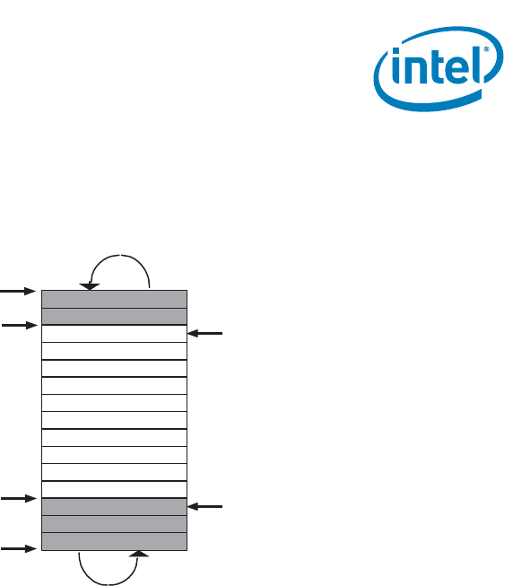
Transmit Descriptor Ring Structure — Intel® 82575EB Gigabit Ethernet Controller
324632-003 Intel® 82575EB Gigabit Ethernet Controller
Revision: 2.1 Software Developer’s Manual and EEPROM Guide
January 2011 145
Descriptors passed to hardware should not be manipulated by software until the head pointer has
advanced past them.
Figure 6. Transmit Descriptor Ring Structure
Shaded boxes in Figure 6 represent descriptors that have been transmitted but not yet reclaimed by
software. Reclaiming involves freeing up buffers associated with the descriptors.
The transmit descriptor ring is described by the following registers:
• Transmit Descriptor Base Address registers (TDBA0-3)
These registers indicate the start address of the descriptor ring buffer in the host memory. This 64-
bit address is aligned on a 16-byte boundary and is stored in two consecutive 32-bit registers.
Hardware ignores the lower 4 bits.
• Transmit Descriptor Length register (TDLEN0-3)
These registers determine the number of bytes allocated to the circular buffer. This value must be
128 byte aligned.
• Transmit Descriptor Head register (TDH0-3)
These registers hold a value which is an offset from the base and indicates the in-progress
descriptor. There can be up to 8 KB descriptors in the circular buffer. Reading these registers return
the value of the head that corresponding to descriptors already loaded in the output FIFO. This
register reflects the internal head of the hardware write-back process including descriptor in the
posted write pipe and might point further ahead than the last descriptor actually written back to
memory.
• Transmit Descriptor Tail register (TDT0-3)
These registers hold a value, which is an offset from the base, and indicates the location beyond the
last descriptor hardware can process. This is the location where software writes the first new
descriptor.
The base register indicates the start of the circular descriptor queue and the length register indicates
the maximum size of the descriptor ring. The lower seven bits of length are hard–wired to 0b. Byte
addresses within the descriptor buffer are computed as follows:
Circular Buffer
Head
Base + Size
Base
Transmit
Queue
Tail
Owned By
Hardware

Intel® 82575EB Gigabit Ethernet Controller — Transmit Descriptor Fetching
Intel® 82575EB Gigabit Ethernet Controller 324632-003
Software Developer’s Manual and EEPROM Guide Revision: 2.1
146 January 2011
address = base + (ptr * 16), where ptr is the value in the hardware head or tail register.
The size chosen for the head and tail registers permit a maximum of 64 K descriptors, or approximately
16 K packets for the transmit queue given an average of four descriptors per packet.
Once activated, hardware fetches the descriptor indicated by the hardware head register. The hardware
tail register points one beyond the last valid descriptor. Software reads the head register to determine
which packets-those logically before the head-have been transferred to the on-chip FIFO or
transmitted.
All the registers controlling the descriptor rings behavior should be set before transmit is enabled, apart
from the tail registers which are used during the regular flow of data.
Note: Software determines if a packet has been sent by either of three methods:
• Setting the RS bit in the transmit descriptor command field or by performing a PIO read of the
transmit head register or by reading the head value written by the 82575 to the address pointed by
the TDWBAL and TDWBAH register.
• Checking the transmit descriptor DD bit or head value in memory eliminates a potential race
condition. All descriptor data is written to the IO bus prior to incrementing the head register, but a
read of the head register could pass the data write in systems performing IO write buffering.
• Updates to transmit descriptors use the same IO write path and follow all data writes.
Consequently, they are not subject to the race.
In general, hardware prefetches packet data prior to transmission. Hardware typically updates the
value of the head pointer after storing data in the transmit FIFO.
5.7.1 Transmit Descriptor Fetching
The descriptor processing strategy for transmit descriptors is essentially the same as for receive
descriptors except that a different set of thresholds are used. As for receives, the number of on-chip
transmit descriptors has been increased (from 8 to 64), and the fetch and write-back algorithms
modified.
When the on-chip buffer is empty, a fetch happens as soon as any descriptors are made available (host
writes to the tail pointer). When the on-chip buffer is nearly empty (TXDCTL[n].PTHRESH), a prefetch is
performed each time enough valid descriptors (TXDCTL[n].HTHRESH) are available in host memory and
no other DMA activity of greater priority is pending (descriptor fetches and write-backs or packet data
transfers).
When the number of descriptors in host memory is greater than the available on-chip descriptor
storage, the chip may elect to perform a fetch which is not a multiple of cache line size. The hardware
performs this non-aligned fetch if doing so results in the next descriptor fetch being aligned on a cache
line boundary. This allows the descriptor fetch mechanism to be most efficient in the cases where it has
fallen behind software.
Note: The 82575 NEVER fetches descriptors beyond the descriptor tail pointer.
5.7.2 Transmit Descriptor Write-Back
The descriptor write-back policy for transmit descriptors is similar to that for receive descriptors with a
few additional factors. First, since transmit descriptor write-backs are optional (controlled by RS in the
transmit descriptor), only descriptors that have one (or both) of these bits set start the accumulation of

TCP Segmentation — Intel® 82575EB Gigabit Ethernet Controller
324632-003 Intel® 82575EB Gigabit Ethernet Controller
Revision: 2.1 Software Developer’s Manual and EEPROM Guide
January 2011 147
write-back descriptors. Secondly, to preserve backward compatibility, if the TXDCTL[n].WTHRESH value
is 0b, the 82575 writes back a single byte of the descriptor (TDESCR.STA) and all other bytes of the
descriptor are left unchanged.
Since the benefit of delaying and then bursting transmit descriptor write-backs is small at best, it is
likely that the threshold are left at the default value (0b) to force immediate write-back of transmit
descriptors and to preserve backward compatibility.
Descriptors are written back in one of three conditions:
• TXDCTL[n].WTHRESH = 0b and a descriptor which has RS set is ready to be written back
• The corresponding EITR counter has reached zero
• TXDCTL[n].WTHRESH > 0b and TXDCTL[n].WTHRESH descriptors have accumulated
For the first condition, write-backs are immediate. This is the default operation and is backward
compatible.
The other two conditions are only valid if descriptor bursting is enabled. In the second condition, the
EITR counter is used to force timely write–back of descriptors. The first packet after timer initialization
starts the timer. Timer expiration flushes any accumulated descriptors and sets an interrupt event
(TXDW).
For the final condition, if TXDCTL[n].WTHRESH descriptors are ready for write-back, the write-back is
performed.
5.8 TCP Segmentation
Hardware TCP Segmentation is one of the off-loading options of most modern TCP/IP stacks. This is
often referred to as Transmit Segmentation Offloading (TSO). This feature enables the TCP/IP stack to
pass to the 82575’s software device driver a message to be transmitted that is bigger than the
Maximum Transmission Unit (MTU) of medium. It is then the responsibility of the software device driver
and hardware to carve the TCP message into MTU size frames that have appropriate layer 2 (Ethernet),
3 (IP), and 4 (TCP) headers. These headers must include sequence number, checksum fields, options
and flag values as required. Note that some of these values (such as the checksum values) are unique
for each packet of the TCP message, and other fields such as the source IP address are constant for all
packets associated with the TCP message.
Padding (TCTL.PSP) must be enabled in TCP segmentation mode, since the last frame might be shorter
than 60 bytes - resulting in a bad frame if PSP is disabled.
The offloading of these mechanisms to the software device driver and the 82575 saves significant CPU
cycles. The software device driver shares the additional tasks to support these options with the 82575.
Note: Although the 82575’s TCP segmentation offload implementation was specifically designed to
take advantage of new “TCP Segmentation offload” features, the hardware implementation
was made generic enough so that it could also be used to “segment” traffic from other
protocols. For instance, this feature could be used any time it is desirable for hardware to
segment a large block of data for transmission into multiple packets that contain the same
generic header.

Intel® 82575EB Gigabit Ethernet Controller — Assumptions
Intel® 82575EB Gigabit Ethernet Controller 324632-003
Software Developer’s Manual and EEPROM Guide Revision: 2.1
148 January 2011
5.8.1 Assumptions
The following assumption applies to the TCP Segmentation implementation in the 82575: The RS bit
operation is not changed. Interrupts are set after data in buffers pointed to by individual descriptors is
transferred to hardware.
5.8.2 Transmission Process
The transmission process for regular (non-TCP Segmentation packets) involves:
• The protocol stack receives from an application a block of data that is to be transmitted.
• The protocol stack calculates the number of packets required to transmit this block based on the
MTU size of the media and required packet headers.
• For each packet of the data block:
— Ethernet, IP and TCP/UDP headers are prepared by the stack.
— The stack interfaces with the software device driver and commands the driver to send the
individual packet.
— The software device driver gets the frame and interfaces with the hardware.
— The hardware reads the packet from host memory (via DMA transfers).
• The software device driver returns ownership of the packet to the operating system when the
hardware has completed the DMA transfer of the frame (indicated by an interrupt).
The transmission process for the 82575 TCP segmentation offload implementation involves:
• The protocol stack receives from an application a block of data that is to be transmitted.
• The stack interfaces to the software device driver and passes the block down with the appropriate
header information.
• The software device driver sets up the interface to the hardware (via descriptors) for the TCP
Segmentation context.
• The hardware transfers the packet data and performs the Ethernet packet segmentation and
transmission based on offset and payload length parameters in the TCP/IP context descriptor
including:
— Packet encapsulation
— Header generation and field updates including IPv4, IPv6 and TCP/UDP checksum generation
• The software device driver returns ownership of the block of data to the operating system when the
hardware has completed the DMA transfer of the entire data block (indicated by an interrupt).
5.8.2.1 TCP Segmentation Data Fetch Control
To perform TCP Segmentation in the 82575, DMA must be able to fit at least one packet of the
segmented payload into available space in the on-chip packet buffer. DMA does various comparisons
between the remaining payload and the packet buffer available space, fetching additional payload and
sending additional packets as space permits.
5.8.3 TCP Segmentation Performance
Performance improvements for a hardware implementation of TCP Segmentation offload mean:

Packet Format — Intel® 82575EB Gigabit Ethernet Controller
324632-003 Intel® 82575EB Gigabit Ethernet Controller
Revision: 2.1 Software Developer’s Manual and EEPROM Guide
January 2011 149
• The stack does not need to partition the block to fit the MTU size (saves CPU cycles).
• The stack only computes one Ethernet, IP, and TCP header per segment (saves CPU cycles).
• The stack interfaces with the software device driver only once per block transfer, instead of once
per frame.
• Larger PCI bursts are used which improves bus efficiency (for example, lowering transaction
overhead).
• Interrupts are easily reduced to one per TCP message instead of one per packet.
• Fewer I/O accesses are required to command the hardware.
5.8.4 Packet Format
Typical TCP/IP transmit window size is 8760 bytes (about 6 full size frames). A TCP message can be as
large as 256 KB and is generally fragmented across multiple pages in host memory. The 82575
partitions the data packet into standard Ethernet frames prior to transmission. The 82575 supports
calculating the Ethernet, IP, TCP, and even UDP headers, including checksum, on a frame by frame
basis.
Figure 7. TCP/IP Packet Format
Frame formats supported by the 82575 include:
• Ethernet 802.3
• IEEE 802.1q VLAN (Ethernet 802.3ac)
• Ethernet Type 2
• Ethernet SNAP
• IPv4 headers with options
• IPv6 headers with extensions
• TCP with options
• UDP with options
VLAN tag insertion is handled by hardware.
UDP (unlike TCP) is not a reliable protocol and fragmentation is not supported at the UDP level. UDP
messages that are larger than the MTU size of the given network medium are normally fragmented at
the IP layer. This is different from TCP, where large TCP messages can be fragmented at either the IP or
TCP layers depending on the software implementation. The 82575 has the ability to segment UDP traffic
(in addition to TCP traffic), however, because UDP packets are generally fragmented at the IP layer, the
82575's TCP Segmentation feature is normally not conducive to handling UDP traffic.
5.8.5 TCP Segmentation Indication
Software indicates a TCP Segmentation transmission context to the hardware by setting up a TCP/ IP
Context Transmit Descriptor. The purpose of this descriptor is to provide information to the hardware to
be used during the TCP segmentation offload process.
Ethernet IPv4/IPv6 TCP/UDP DATA FCS

Intel® 82575EB Gigabit Ethernet Controller — TCP Segmentation Indication
Intel® 82575EB Gigabit Ethernet Controller 324632-003
Software Developer’s Manual and EEPROM Guide Revision: 2.1
150 January 2011
Setting the TSE bit in the TUCMD field to 1b indicates that this descriptor refers to the TCP
Segmentation context (as opposed to the normal checksum offloading context). This causes the
checksum offloading, packet length, header length, and maximum segment size parameters to be
loaded from the descriptor into the 82575.
The TCP Segmentation prototype header is taken from the packet data itself. Software must identity
the type of packet that is being sent (IPv4/IPv6, TCP/UDP, other), calculate appropriate checksum
offloading values for the desired checksums, and calculate the length of the header which is pre-
pended. The header can be up to 240 bytes in length.
Once the TCP Segmentation context has been set, the next descriptor provides the initial data to
transfer. This first descriptor(s) must point to a packet of the type indicated. Furthermore, the data it
points to might need to be modified by software as it serves as the prototype header for all packets
within the TCP Segmentation context. The following sections describe the supported packet types and
the various updates that are performed by hardware. This should be used as a guide to determine what
must be modified in the original packet header to make it a suitable prototype header.
The following summarizes the fields considered by the software device driver for modification in
constructing the prototype header:
• IP Header:
— Length should be set to zero
• For IPv4 Headers:
— Identification field should be set as appropriate for first packet of send (if not already)
— Header checksum should be zeroed out unless some adjustment is needed by the software
device driver
• TCP Header:
— Sequence number should be set as appropriate for first packet of send (if not already)
— PSH and FIN flags should be set as appropriate for last packet of send
— TCP checksum should be set to the partial pseudo-header checksum as follows:
Figure 8. TCP Partial Pseudo-Header Checksum for IPv6
Figure 9. TCP Partial Pseudo-Header Checksum for IPv4
IP Source Address
IP Destination Address
Zero Layer 4 Protocol ID Zero
IPv6 Source Address
IPv6 Final Destination Address
Zero
Zero Next Header
IP and TCP/UDP Headers — Intel® 82575EB Gigabit Ethernet Controller
324632-003 Intel® 82575EB Gigabit Ethernet Controller
Revision: 2.1 Software Developer’s Manual and EEPROM Guide
January 2011 151
• UDP Header:
— The 82575’s DMA function fetches the Ethernet, IP, and TCP/UDP prototype header information
from the initial descriptor(s) and save them on-chip for individual packet header generation.
The following sections describe the updating process performed by the hardware for each frame
sent using the TCP Segmentation capability.
5.8.6 IP and TCP/UDP Headers
This section outlines the format and content for the IP, TCP and UDP headers. The 82575 requires
baseline information from the software device driver in order to construct the appropriate header
information during the segmentation process.
Header fields that are modified by the 82575 are highlighted in the figures that follow.
Note: IPv4 requires the use of a checksum for the header. IPv6 does not use a header Checksum.
IPv4 length includes the TCP and IP headers as well as data. IPv6 length does not include
the IPv6 header.
The IPv4 header is first shown in the traditional (RFC 791) representation, and because byte and bit
ordering is confusing in that representation, the IP header is also shown in little-endian format. The
actual data is fetched from memory in little-endian format.
Figure 10. IPv4 Header (Traditional Representation)
1 2 3
0 1 2 3 4 5 6 7 8 9 0 1 2 3 4 5 6 7 8 9 0 1 2 3 4 5 6 7 8 9 0 1
Version IP Hdr
Length
TYPE of service Total length
Identification Flags Fragment Offset
Time to Live Layer 4 Protocol ID Header Checksum
Source Address
Destination Address
Options
Byte3 Byte2 Byte1 Byte0
7 6 5 4 3 2 1 0 7 6 5 4 3 2 1 0 7 6 5 4 3 2 1 0 7 6 5 4 3 2 1 0
LSB Total length MSB TYPE of Service Version IP Hdr
Length
Fragment Offset Low R
E
S
N
F
M
F
Fragment Offset
High
LSB Identification MSB
Header Checksum Layer 4 Protocol ID Time to Live
Source Address
Destination Address
Options

Intel® 82575EB Gigabit Ethernet Controller — IP and TCP/UDP Headers
Intel® 82575EB Gigabit Ethernet Controller 324632-003
Software Developer’s Manual and EEPROM Guide Revision: 2.1
152 January 2011
Figure 11. IPv4 Header (Little-Endian Order)
Note: Identification is incremented on each packet.
Flags Field Definition:
The Flags field is defined below. Note that hardware does not evaluate or change these bits.
• MF - More Fragments
• NF - No Fragments
• Reserved
The 82575 does TCP segmentation not IP fragmentation. IP fragmentation might occur in transit
through a network’s infrastructure.
Figure 12. IPv6 TCP Header (Traditional Representation)
Figure 13. IPv6 Header (Little Endian Order)
A TCP or UDP frame uses a 16 bit wide one’s complement checksum. The checksum word is computed
on the outgoing TCP or UDP header and payload, and on the Pseudo Header. Details on checksum
computations are provided in Section 3.8.
Note: TCP and UDP over IPv6 requires the use of checksum, where it is optional for UDP over
IPv4.
1 2 3
0 1 2 3 4 5 6 7 8 9 0 1 2 3 4 5 6 7 8 9 0 1 2 3 4 5 6 7 8 9 0 1
Version Priority Flow Label
Payload Length Next Header Type Hop Limit
Source Address
Destination Address
Extensions (if any)
Byte3 Byte2 Byte1 Byte0
7 6 5 4 3 2 1 0 7 6 5 4 3 2 1 0 7 6 5 4 3 2 1 0 7 6 5 4 3 2 1 0
Flow Label Version Priority
Hop Limit Next Header Type LSB Payload Length MSB
Source Address
Destination Address
Extensions
IP and TCP/UDP Headers — Intel® 82575EB Gigabit Ethernet Controller
324632-003 Intel® 82575EB Gigabit Ethernet Controller
Revision: 2.1 Software Developer’s Manual and EEPROM Guide
January 2011 153
The TCP header is first shown in the traditional (RFC 793) representation. Because byte and bit
ordering is confusing in that representation, the TCP header is also shown in little-endian format. The
actual data is fetched from memory in little-endian format.
Figure 14. TCP Header (Traditional Representation)
Figure 15. TCP Header (Little Endian)
The TCP header is always a multiple of 32 bit words. TCP options may occupy space at the end of the
TCP header and are a multiple of 8 bits in length. All options are included in the checksum.
The checksum also covers a 96-bit pseudo header conceptually prefixed to the TCP Header. The IPv4
pseudo header contains the IPv4 Source Address, the IPv4 Destination Address, the IPv4 Protocol field,
and TCP Length. The IPv6 pseudo header contains the IPv6 Source Address, the IPv6 Destination
Address, the IPv6 Payload Length, and the IPv6 Next Header field. Software pre-calculates the PARTIAL
pseudo header sum, which includes IPv4 SA, DA and protocol types, but NOT the TCP length, and
stores this value into the TCP checksum field of the packet. For both IPv4 and IPv6, hardware needs to
factor in the TCP length to the software supplied pseudo header partial checksum.
Note: The Protocol ID field should always be added the least significant byte (LSB) of the 16 bit
pseudo header sum, where the most significant byte (MSB) of the 16 bit sum is the byte
that corresponds to the first checksum byte out on the wire.
The TCP Length field is the TCP Header Length including option fields plus the data length in bytes,
which is calculated by hardware on a frame by frame basis. The TCP Length does not count the 12 bytes
of the pseudo header. The TCP length of the packet is determined by hardware as:
1 2 3
0 1 2 3 4 5 6 7 8 9 0 1 2 3 4 5 6 7 8 9 0 1 2 3 4 5 6 7 8 9 0 1
Source Port Destination Port
Sequence Number
Acknowledgement Number
TCP Header
Length
Reserved U
R
G
A
C
K
P
S
H
R
S
T
S
Y
N
F
I
N
Window
Checksum Urgent Pointer
Options
Byte3 Byte2 Byte1 Byte0
7 6 5 4 3 2 1 0 7 6 5 4 3 2 1 0 7 6 5 4 3 2 1 0 7 6 5 4 3 2 1 0
Destination Port Source Port
LSB Sequence Number MSB
Acknowledgement Number
Window R E
S
U
R
G
A
C
K
P
S
H
R
S
T
S
Y
N
FI
N
TCP Header
Length
Reserved
Urgent Pointer Checksum
Options

Intel® 82575EB Gigabit Ethernet Controller — IP and TCP/UDP Headers
Intel® 82575EB Gigabit Ethernet Controller 324632-003
Software Developer’s Manual and EEPROM Guide Revision: 2.1
154 January 2011
TCP Length = min(PAYLOADLEN) + L5_LEN
The two flags that might be modified are defined as:
• PSH: Receiver should pass this data to the application without delay
• FIN: Sender is finished sending data
The handling of these flags is described in Section 5.8.7.
Payload is normally MSS except for the last packet where it represents the remainder of the payload.
Figure 16. TCP Pseudo Header Content (Traditional Representation)
The Layer 4 Protocol ID value in the pseudo-header identifies the upper-layer protocol (6 for TCP or 17
for UDP).
Figure 17. TCP/UDP Pseudo Header Content for IPv6 (Traditional Representation)
Note: If the IPv6 packet contains a routing header, the destination address used in the pseudo-
header is that of the final destination. At the originating node, that address is in the last
element of the routing header; at the recipient(s), that address is in the Destination
Address field of the IPv6 header.
The next header value in the pseudo-header identifies the upper-layer protocol (6 for TCP or 17 for
UDP). It differs from the next header value in the IPv6 header if there are extension headers between
the IPv6 header and the upper-layer header.
The upper-layer packet length in the pseudo-header is the length of the upper-layer header and data
(TCP header plus TCP data). Some upper-layer protocols carry their own length information (for
example, the Length field in the UDP header); for such protocols, that is the length used in the pseudo-
header. Other protocols (such as TCP) do not carry their own length information, in which case the
length used in the pseudo-header is the payload length from the IPv6 header minus the length of any
extension headers present between the IPv6 header and the upper-layer header.
Unlike IPv4, when UDP packets are originated by an IPv6 node, the UDP checksum is not optional.
Whenever originating a UDP packet, an IPv6 node must compute a UDP checksum over the packet and
the pseudo-header and if that computation yields a result of zero, it must be changed to FFFFh for
placement in the UDP header. IPv6 receivers must discard UDP packets containing a zero checksum and
should log the error.
IPv4 Source Address
IPv4 Destination Address
Zero Layer 4 Protocol ID TCP Length
IPv6 Source Address
IPv6 Final Destination Address
TCP Packet Length
Zero Next Header

IP and TCP/UDP Headers — Intel® 82575EB Gigabit Ethernet Controller
324632-003 Intel® 82575EB Gigabit Ethernet Controller
Revision: 2.1 Software Developer’s Manual and EEPROM Guide
January 2011 155
A type 0 routing header contains the following format:
Figure 18. IPv6 Routing Header (Traditional Representation)
• Next Header - 8-bit selector. Identifies the type of header immediately following the routing header.
Uses the same values as the IPv4 Protocol field [RFC-1700 et seq.].
• Header Extension Length - 8-bit unsigned integer. Length of the routing header in 8-octet units, not
including the first 8 octets. For the Type 0 Routing header, Header Extension Length is equal to two
times the number of addresses in the header.
• Routing Type - 0
• Segments Left - 8-bit unsigned integer. Number of route segments remaining. For example, the
number of explicitly listed intermediate nodes still to be visited before reaching the final
destination. Equal to "n" at the source node.
• Reserved - 32-bit reserved field. Initialized to zero for transmission; ignored on reception.
• Address[1...n] - Vector of 128-bit addresses, numbered 1 to n.
The 82575 supports checksum off-loading as a component of the TCP Segmentation offload feature and
as a standalone capability. Section 3.8.7 describes the interface for controlling the checksum off-
loading feature. This section describes the feature as it relates to TCP Segmentation.
The 82575 supports IP and TCP/UDP header options in the checksum computation for packets that are
derived from the TCP Segmentation feature.
Note: The 82575 is capable of computing one level of IP header checksum and one TCP/UDP
header and payload checksum. In case of multiple IP headers, the driver has to compute all
but one IP header checksum. The 82575 calculates checksums on the fly on a frame by
frame basis and inserts the result in the IP/TCP/UDP headers of each frame. TCP and UDP
checksum are a result of performing the checksum on all bytes of the payload and the
pseudo header.
Three specific types of checksum are supported by the hardware in the context of the TCP
Segmentation offload feature:
• IPv4 checksum
• TCP checksum
• UDP checksum
Each packet that is sent via the TCP segmentation offload feature optionally includes the IPv4
checksum and either the TCP or UDP checksum.
Next Header Hdr Ext Len Routing Type 0 Segments Left n
Reserved
Address[1]
Address[2]
…
Final Destination Address[n]
Intel® 82575EB Gigabit Ethernet Controller — IP/TCP/UDP Header Updating
Intel® 82575EB Gigabit Ethernet Controller 324632-003
Software Developer’s Manual and EEPROM Guide Revision: 2.1
156 January 2011
All checksum calculations use a 16-bit wide one’s complement checksum. The checksum word is
calculated on the outgoing data. The checksum field is written with the 16 bit one’s complement of the
one’s complement sum of all 16-bit words in the range of CSS to CSE, including the checksum field
itself.
Table 47. Supported Transmit Checksum Capabilities
Table 48 lists the conditions of when checksum offloading can/should be calculated.
Table 48. Calculating Checksum Offloading
5.8.7 IP/TCP/UDP Header Updating
IP/TCP/UDP header is updated for each outgoing frame based on the IP/TCP header prototype which
hardware transfers from the first descriptor(s) and stores on chip. The IP/TCP/UDP headers are fetched
from host memory into an on-chip 512 byte header buffer once for each TCP segmentation context (for
performance reasons, this header is not fetched again for each additional packet that is derived from
the TCP segmentation process). The checksum fields and other header information are later updated on
a frame by frame basis. The updating process is performed concurrently with the packet data fetch.
The following sections define which fields are modified by hardware during the TCP Segmentation
process by the 82575.
Note: Software must make the PAYLEN and HDRLEN values of context descriptors correct.
Otherwise, the failure of large send due to either under-run or over-run might cause
hardware to send bad packets or even cause transmit hardware to hang. The indication of
large send failure can be checked in the TSCTFC statistic register.
Packet Type HW IP Checksum Calculation HW TCP/UDP Checksum
Calculation
IPv4 packets Yes Yes
IPv6 packets
(no ip checksum in Ipv6)
NA Yes
Packet is greater than 1552 bytes; (LPE = 1b) Yes Yes
Packet has 802.3ac tag Yes Yes
Packet has IP options
(IP header is longer than 20 bytes)
Yes Yes
Packet has TCP or UDP options Yes Yes
IP header’s protocol field contains a protocol # other than
TCP or UDP
Yes No
Packet Type IPv4 TCP/UDP Reason
Non TSO Yes No IP raw packet (non TCP/UDP protocol)
Yes Yes TCP segment or UDP datagram with checksum offload
No No Non-IP packet or checksum not offloaded
TSO Yes Yes For TSO, checksum offload must be done

IP/TCP/UDP Header Updating — Intel® 82575EB Gigabit Ethernet Controller
324632-003 Intel® 82575EB Gigabit Ethernet Controller
Revision: 2.1 Software Developer’s Manual and EEPROM Guide
January 2011 157
5.8.7.1 TCP/IP/UDP Header for the First Frame
The hardware makes the following changes to the headers of the first packet that is derived from each
TCP segmentation context.
• MAC Header (for SNAP)
— Type/Len field = MSS + MACLEN + IPLEN + L4LEN - 14
• IPv4 Header
— IP Total Length = MSS + L4LEN – IPLEN
— IP Checksum
• IPv6 Header
— Payload Length = MSS + L4LEN + IPV6_HDR_extension
• TCP Header
— Sequence Number: The value is the sequence number of the first TCP byte in this frame.
— If FIN flag = 1b, it is cleared in the first frame.
— If PSH flag =1b, it is cleared in the first frame.
— TCP Checksum
• UDP Header
— UDP length: MSS + L4LEN
— UDP Checksum
5.8.7.2 TCP/IP/UDP Header for the Subsequent Frames
The hardware makes the following changes to the headers for subsequent packets that are derived as
part of a TCP segmentation context:
Note: Number of bytes left for transmission = PAYLEN – (N * MSS). Where N is the number of
frames that have been transmitted.
• MAC Header (for SNAP packets)
— Type/LEN field = MSS + MACLEN + IPLEN + L4LEN – 14
• IPv4 Header
— IP Identification: incremented from last value (wrap around)
— IP Total Length = MSS + L4LEN + IPLEN
— IP Checksum
• IPv6 Header
— Payload Length = MSS + L4LEN + IPV6_HDR_extension
• TCP Header
— Sequence Number update: Add previous TCP payload size to the previous sequence number
value. This is equivalent to adding the MSS to the previous sequence number.
— If FIN flag = 1b, it is cleared in these frames.
— If PSH flag =1b, it is cleared in these frames.
— TCP Checksum
• UDP Header
— UDP Length: MSS + L4LEN

Intel® 82575EB Gigabit Ethernet Controller — IP/TCP/UDP Transmit Checksum Offloading
Intel® 82575EB Gigabit Ethernet Controller 324632-003
Software Developer’s Manual and EEPROM Guide Revision: 2.1
158 January 2011
— UDP Checksum
5.8.7.3 TCP/IP/UDP Header for the Last Frame
Hardware makes the following changes to the headers for the last frame of a TCP segmentation
context:
Note: Last frame payload bytes = PAYLEN – (N * MSS)
• MAC Header (for SNAP packets)
— Type/LEN field = last frame payload bytes + MACLEN + IPLEN + L4LEN – 14
• IPv4 Header
— IP Total Length = last frame payload bytes + L4LEN) + IPLEN
— IP Identification: incremented from last value (wrap around configurable based on a 15 bit
width or 16-bit width)
— IP Checksum
• IPv6 Header
— Payload Length = last frame payload bytes + L4LEN + IPV6_HDR_extension
• TCP Header
— Sequence Number update: Add previous TCP payload size to the previous sequence number
value. This is equivalent to adding the MSS to the previous sequence number.
— If FIN flag = 1b, set it in this last frame
— If PSH flag =1b, set it in this last frame
— TCP Checksum
• UDP Header
— UDP length: last frame payload bytes + L4LEN
— UDP Checksum
5.9 IP/TCP/UDP Transmit Checksum
Offloading
The 82575 performs checksum offloading as an optional part of the TCP/UDP segmentation offload
feature. These specific checksums are supported under TCP segmentation:
• IPv4 checksum
• TCP checksum
• UDP checksum
Checksum offloading can also be performed in a single-send packet.
Note: For tunneled packets, hardware can perform either an IPv4 checksum or TCP checksum but
not both.

IP/TCP/UDP Transmit Checksum Offloading in Non-Segmentation Mode — Intel® 82575EB
Gigabit Ethernet Controller
324632-003 Intel® 82575EB Gigabit Ethernet Controller
Revision: 2.1 Software Developer’s Manual and EEPROM Guide
January 2011 159
5.10 IP/TCP/UDP Transmit Checksum
Offloading in Non-Segmentation Mode
The previous section on TCP Segmentation offload describes the IP/TCP/UDP checksum offloading
mechanism used in conjunction with TCP Segmentation. The same underlying mechanism can also be
applied as a standalone feature. The main difference in normal packet mode (non-TCP Segmentation) is
that only the checksum fields in the IP/TCP/UDP headers need to be updated.
Before taking advantage of the 82575’s enhanced checksum offload capability, a checksum context
must be initialized. For the normal transmit checksum offload feature this is performed by providing the
82575 with a TCP/IP Context Descriptor with TUCMD.TSE = 0b. Setting TSE = 0b indicates that the
normal checksum context is being set, as opposed to the segmentation context.
Note: Enabling the checksum offloading capability without first initializing the appropriate
checksum context leads to unpredictable results. CRC appending (DCMD.IFCS) must be
enabled in TCP/IP checksum mode, since CRC must be inserted by hardware after the
checksums have been calculated.
As mentioned in Section 5.7, it is not necessary to set a new context for each new packet. In many
cases, the same checksum context can be used for a majority of the packet stream. In this case, some
performance can be gained by only changing the context on an as needed basis or electing to use the
offload feature only for a particular traffic type, thereby avoiding all context descriptors except for the
initial one.
Each checksum operates independently. Inserting IP and TCP checksums for each packet are enabled
through the Transmit Data Descriptor POPTS.TSXM and POPTS.IXSM fields, respectively.
5.10.1 IP Checksum
Three fields in the Transmit Context Descriptor set the context of the IP checksum offloading feature:
• TUCMD.IPv4
• IPLEN
• MACLEN
TUCMD.IPv4 = 1b specifies that the packet type for this context is IPv4 and that the IP header
checksum should be inserted. TUCMD.IPv4 = 0b indicates that the packet type is IPv6 (or some other
protocol) and that the IP header checksum should not be inserted.
MACLEN specifies the byte offset from the start of the transferred data to the first byte to be included in
the checksum, the start of the IP header. The minimal allowed value for this field is 12. Note that the
maximum value for this field is 255 which is adequate for typical applications.
Note: The MACLEN+IPLEN value needs to be less than the total DMA length for a packet. If this is
not the case, the results will be unpredictable.
IPLEN specifies where the IP checksum should stop. Again, this is limited to the first 256 bytes of the
packet and must be less than or equal to the total length of a given packet. If this is not the case, the
checksum is not inserted.
The 16-bit IPv4 header checksum is placed at the two bytes starting at MACLEN+10.

Intel® 82575EB Gigabit Ethernet Controller — TCP Checksum
Intel® 82575EB Gigabit Ethernet Controller 324632-003
Software Developer’s Manual and EEPROM Guide Revision: 2.1
160 January 2011
As mentioned in Section 5.6.2, it is not necessary to set a new context for each new packet. In many
cases, the same checksum context can be used for a majority of the packet stream. In this case, some
performance can be gained by only changing the context on an as needed basis or electing to use the
offload feature only for a particular traffic type, thereby avoiding all context descriptors except for the
initial one.
5.10.2 TCP Checksum
Three fields in the Transmit Context Descriptor set the context of the TCP checksum offloading feature:
• MACLEN
• IPLEN
• TUCMD.L4T
TUCMD.TCPL4T = 1b specifies that the packet type is TCP, and that the 16-bit TCP header checksum
should be inserted at byte offset MACLEN + IPLEN + 16. TUCMD.L4T = 0b indicates that the packet is
UDP and that the 16-bit checksum should be inserted starting at byte offset MACLEN + IPLEN + 6.
IPLEN+MACLEN specifies the byte offset from the start of the transferred data to the first byte to be
included in the checksum, the start of the TCP header. The minimal allowed value for this sum is 18/28
for UDP or TCP, respectively. Note that the maximum value for this field is 255 and is adequate for
typical applications.
Note: The IPLEN + MACLEN + L4LEN value needs to be less than the total transfer length for a
packet. If not, results are unpredictable.
The TCP/UDP checksum always continues to the last byte of the transferred data.
Note: For non-TSO, software still needs to calculate a full checksum for the TCP/UDP pseudo-
header. This checksum of the pseudo-header should be placed in the packet data buffer at
the appropriate offset for the checksum calculation.
5.11 Multiple Transmit Queues
The number of transmit queues for the 82575 has increased to four, to match the expected number of
processors on most server platforms. If there are more processors than queues, then one queue can be
used to service more than one processor.
In transmission, each processor sets a queue in the host memory (this memory is likely to be the one
that is closely connected to the processor).
Transmission priority among the queues is under software configuration and meets the following rules:
• Arbitration between queues is done at the segment boundary. That is, once a segment (including a
TSO segment) is selected for transmission, it would complete transmitting before another packet is
selected.
• Each queue can be assigned as High Priority (HP) or Low Priority (LP). Software can change priority
any time during operation.
• HP queues are always selected before LP queues. Note that this might cause starvation of the LP
queues.
• Round robin arbitration is performed among the HP queues.
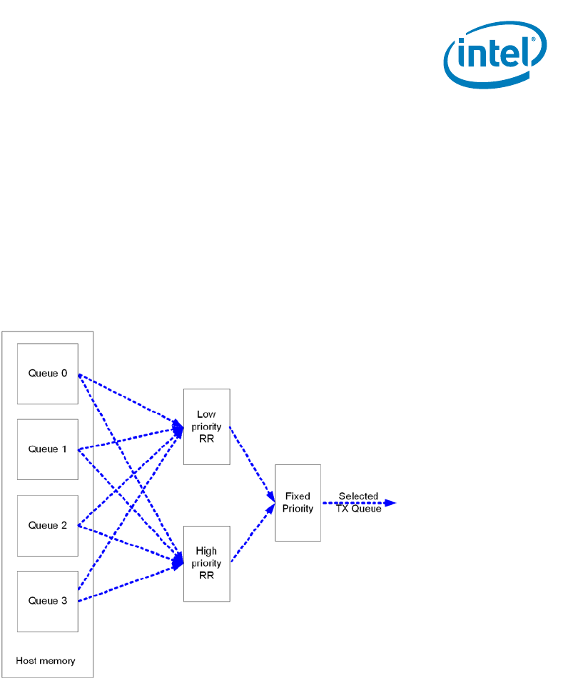
Tx Completions Head Write-Back — Intel® 82575EB Gigabit Ethernet Controller
324632-003 Intel® 82575EB Gigabit Ethernet Controller
Revision: 2.1 Software Developer’s Manual and EEPROM Guide
January 2011 161
• Round robin arbitration is performed among the LP queues.
Note: In order to prevent starvation, HP queues should not be used for TSO requests. Software
must enforce this; it is not enforced by the 82575.
Software should also change the priority bit only when a queue is empty and it is guaranteed that the
82575 is not engaged in fetching Tx packets for the given queue.
The following scheme avoids excessive latency of transmit packets queued simultaneously with TSO
packets. TSO packets take tens of s (or more) to transmit. A packet queued behind several TSO
packets would suffer from an additional latency of tens to hundreds of s. This is unacceptable in some
applications where low latency is a requirement.
Figure 19. Multiple Queues in Transmit
5.12 Tx Completions Head Write-Back
In legacy hardware, transmit requests are completed by writing the DD bit to the transmit descriptor
ring. This causes cache thrash since both the software device driver and hardware are writing to the
descriptor ring in host memory. Instead of writing the DD bits to signal that a transmit request is
complete, hardware writes the contents of the descriptor queue head to host memory. The software
device driver reads that memory location to determine which transmit requests are complete. In order
to improve the performance of this feature, the software device driver needs to program DCA registers
to configure which CPU will process each TX queue.
The head counter is reflected in a memory location that is allocated by software for each queue.

Intel® 82575EB Gigabit Ethernet Controller — Interrupts
Intel® 82575EB Gigabit Ethernet Controller 324632-003
Software Developer’s Manual and EEPROM Guide Revision: 2.1
162 January 2011
Head write-back occurs if TDWBAL#.Head_WB_En is set for this queue and the RS bit is set in the Tx
descriptor, following corresponding data upload into packet buffer.
The software device driver has control on this feature through Tx Queue 0-3 head write-back address,
low and high (enabling a 64-bit address).
The low register’s LSB hold the control bits.
• The Head_WB_En bit enables activation of tail write-back. In this case, no descriptor write-back is
executed.
• The SN_WB_en bit enables both the DD and the sequence number bit write-back into the descriptor
address.
• The 30 upper bits of this register hold the lowest 32 bits of the head write-back address, assuming
that the two last bits are set to 0b.
The high register holds the high part of the 64-bit address. The 82575 only writes the 16 bits that are
pointed by TDWBAH/TDWBAL address.
5.13 Interrupts
The interrupt logic consists of the 10 registers listed in Table 49 plus the registers associated with MSI/
MSI-X signaling.
Table 49. Interrupt Registers
5.13.1 Interrupt Cause Register (ICR)
This register captures the interrupt causes not directly captured by the EICR. These are infrequent
management interrupts and error conditions.
Register Acronym Function
Interrupt Cause ICR Records interrupt conditions.
Interrupt Cause Set ICS Allows software to set bits in the ICR.
Interrupt Mask Set/Read IMS Sets or reads bits in the other interrupt mask.
Interrupt Mask Clear IMC Clears bits in the other interrupt mask.
Interrupt Acknowledge
auto-mask
IAM Under some conditions, the content of this register is copied to the mask register
following read or write of ICR.
Extended Interrupt
Cause
EICR ICR. Records interrupt causes from receive and transmit queues. An interrupt is
signaled when unmasked bits in this register are set.
Extended Interrupt
Cause Set
EICS Enables software to set bits in the ICR.
Extended Interrupt
Mask Set/Read
EIMS Sets or read bits in the interrupt mask.
Extended Interrupt
Mask Clear
EIMC Clears bits in the interrupt mask.
Extended Interrupt Auto
Clear
EIAC Enables bits in the EICR to be cleared automatically following an MSI-X interrupt
without a read or write of the EICR.
Extended Interrupt
Acknowledge Auto-Mask
EIAM This register is used to decide which masks are cleared in the extended mask
register following read or write of EICR or which masks are set following a write
to EICS. In MSI-X mode, this register also controls which bits in EIMC are cleared
automatically following an MSI-X interrupt.

Interrupt Cause Set Register (ICS) — Intel® 82575EB Gigabit Ethernet Controller
324632-003 Intel® 82575EB Gigabit Ethernet Controller
Revision: 2.1 Software Developer’s Manual and EEPROM Guide
January 2011 163
Note: When EICR is used in MSI-X mode, the Rx / Tx related bits in ICR should be masked.
5.13.2 Interrupt Cause Set Register (ICS)
This registers enables setting the bits of ICR by software, by writing a 1b in the corresponding bits in
ICS. Used to rearm interrupts software did not have time to handle in the current interrupt routine.
5.13.3 Interrupt Mask Set/Read Register (IMS)
An interrupt is enabled if its corresponding mask bit in this register is set to 1b and disabled if its
corresponding mask bit is set to 0b. A PCIe* interrupt is generated each time one of the bits in this
register is set and the corresponding interrupt condition occurs. The occurrence of an interrupt
condition is reflected by having a bit set in the ICR.
Reading this register returns which bits have an interrupt mask set.
A particular interrupt can be enabled by writing a 1b to the corresponding mask bit in this register. Any
bits written with a 0b are unchanged. Therefore, if software desires to disable a particular interrupt
condition that had been previously enabled, it must write to the IMC instead of writing a 0b to a bit in
this register.
5.13.4 Interrupt Mask Clear Register (IMC)
Software blocks interrupts by clearing the corresponding mask bit. This is accomplished by writing a 1b
to the corresponding bit in this register. Bits written with 0b are unchanged (their mask status does not
change).
5.13.5 Interrupt Acknowledge Auto-mask register
(IAM)
An ICR read or write has the side effect of writing the contents of this register to the IMC register. If
CTRL_EXT.NSICR = 0b, then the copy of this register to IMS only occurs after at least one bit is set in
the IMS and there is a true interrupt as reflected in ICR.INTA.
5.13.6 Extended Interrupt Cause Registers (EICR)
This register records the non-error interrupts from the receive and transmit queues in a unique bit per
queue plus one bit to indicate when any interrupt in the ICR is active. Bits in this register can be
configured to auto-clear when the MSI-X interrupt message is sent in order to minimize software device
driver overhead when using MSI-X interrupt signaling.
In systems that do not support MSI-X, writing 1b's clears the corresponding bits in this register. Most
systems have write- buffering that minimizes overhead, but this might require a read operation to
guarantee that the write has been flushed from posted buffers. Reading this register auto-clears all
bits.

Intel® 82575EB Gigabit Ethernet Controller — Extended Interrupt Cause Set Register (EICS)
Intel® 82575EB Gigabit Ethernet Controller 324632-003
Software Developer’s Manual and EEPROM Guide Revision: 2.1
164 January 2011
5.13.7 Extended Interrupt Cause Set Register (EICS)
This registers enables the setting of bits in EICR, by software, by writing a 1b in the corresponding bits
in EICS. Used to rearm interrupts software did not have time to handle in the current interrupt routine.
5.13.8 Extended Interrupt Mask Set and Read Register
(EIMS)/Extended Interrupt Mask Clear Register
(EIMC)
Interrupts appear on PCIe* only if the interrupt cause bit is set to 1b and the corresponding interrupt
mask bit is set to 1b. Software blocks asserting an interrupt by clearing the corresponding bit in the
mask register. The cause bit stores the interrupt event regardless of the state of the mask bit. Clear and
set make this register more thread safe by avoiding a read-modify-write operation on the mask
register. The mask bit is set for each bit written to a one in the set register and cleared for each bit
written in the clear register. Reading the set register (EIMS) returns the current mask register value.
5.13.9 Extended Interrupt Auto Clear Enable Register
(EIAC)
Each bit in this register enables clearing of the corresponding bit in EICR following interrupt generation.
When a bit is set, the corresponding bit in EICR is automatically cleared following an interrupt. This
feature should only be used in MSI-X mode.
When used in conjunction with MSI-X interrupt vector, this feature enables interrupt cause recognition
and selective interrupt cause without requiring software to read or write the EICR register; therefore,
the penalty related to a PCIe* read or write transaction is avoided (Section 5.15).
5.13.10 Extended Interrupt Auto Mask Enable Register
(EIAM)
Each bit set in this register enables clearing of the corresponding bit in EIMS following read or write-to-
clear to EICR. It also enables setting of the corresponding bit in EIMS following a write-to-set to EICS.
This mode is provided in case MSI-X is not used. As a result, auto-clear through EIAC register is not
available.
In MSI-X mode, the software device driver might set the bits of this register to select mask bits that are
reset during interrupt processing. In this mode, each bit in this register enables clearing of the
corresponding bit in EIMC following interrupt generation.

Interrupt Modes Setting Bits — Intel® 82575EB Gigabit Ethernet Controller
324632-003 Intel® 82575EB Gigabit Ethernet Controller
Revision: 2.1 Software Developer’s Manual and EEPROM Guide
January 2011 165
5.13.11 Interrupt Modes Setting Bits
There are bits in the CTRL_EXT register that define the behavior of the interrupt mechanism. Setting
these bits is different in each mode of operation. The following table describes the recommended
setting of these bits in the different modes:
5.14 Interrupt Moderation
An interrupt is generated upon receiving of incoming packets, as throttled by the EITR registers. There
are 10 EITR registers; each one is allocated to a vector of MSI-X.
When the MSI-X interrupt is activated, each active bit in EICR can trigger an interrupt vector. The
allocation of MSI-X vectors to each bit of EICR is set by the setting the MSI_X_ALLOC[09:0] registers.
Following the allocation, the EITR corresponding to the MSI-X vector is tied to one or more bits in EICR.
When MSI-X is not activated, the interrupt moderation is controlled by EITR[0].
Software can use EITR to limit the rate of delivery of interrupts to the host processor. This register
provides a guaranteed inter-interrupt delay between interrupts asserted by the 82575, regardless of
network traffic conditions.
The following algorithm can be used to convert the inter-interrupt interval value to the common
interrupts/sec performance metric:
interrupts/sec = (256 10-9sec interval)-1
For example, if the interval is programmed to 500d, the 82575 guarantees the CPU is not interrupted
by the 82575 for at least 128 microseconds from the last interrupt. The maximum observable interrupt
rate from the 82575 should not exceed 7813 interrupts/sec.
Field Bit(s) Initial
Value Description INT-x/
MSI +
Legacy
INT-x/
MSI +
Extend MSI-X
NSICR 0 0b Non Selective Interrupt Clear on Read
When set, every read of ICR clears it. When this bit is
cleared, an ICR read causes it to be cleared only if an actual
interrupt was asserted or IMS = 0b. This bit should be
cleared by drivers not using the extended interrupts
capabilities and set otherwise.
0b1
1. In systems where interrupt sharing is not expected, the NSICR bit can also be set by legacy drivers.
1b 1b
EIAME 24 0b Extended Interrupt Auto Mask Enable
When set (usually in MSI-X mode), upon firing of an MSI-X
message, bits set in EIAM associated with this message are
cleared. Otherwise, EIAM is used only upon read or write of
EICR/EICS registers.
0b 0b 1b
PBA_
support
31 0b PBA Support
When set, setting one of the extended interrupts masks via
EIMS causes the PBA bit of the associated MSI-X vector to
be cleared. Otherwise, the 82575 behaves in a way
supporting legacy INT-x interrupts.
Should be cleared when working in INT-x or MSI mode and
set in MSI-X mode.
0b 0b 1b

Intel® 82575EB Gigabit Ethernet Controller — Interrupt Moderation
Intel® 82575EB Gigabit Ethernet Controller 324632-003
Software Developer’s Manual and EEPROM Guide Revision: 2.1
166 January 2011
Inversely, inter-interrupt interval value can be calculated as:
inter-interrupt interval = (256 10-9sec interrupts/sec)-1
The optimal performance setting for this register is very system and configuration specific. An initial
suggested value is 4000 (one interrupt every 250 s).
The EITR should default to 0b upon initialization and reset. It loads in the value programmed by the
software after software initializes the 82575.
When software wants to force an immediate interrupt, for example, after setting a bit in the EICR with
the EICS register, the value of the counter can be written to 0b to generate an immediate interrupt.
This write should include re-writing the Interval field with the desired constant, as it will be used to
reload the counter immediately for the next throttling interval.
The 82575 implements interrupt moderation to reduce the number of interrupts software processes.
The moderation scheme is based on EITR. Each time an interrupt event happens, the corresponding bit
in the EICR is activated. However, an interrupt message is not sent out on the PCIe* interface until the
EITR counter assigned to that EICR bit has counted down to zero. As soon as the interrupt is issued, the
EITR counter is reloaded with its initial value and the process repeats again. The interrupt flow should
follow as shown in Figure 20.
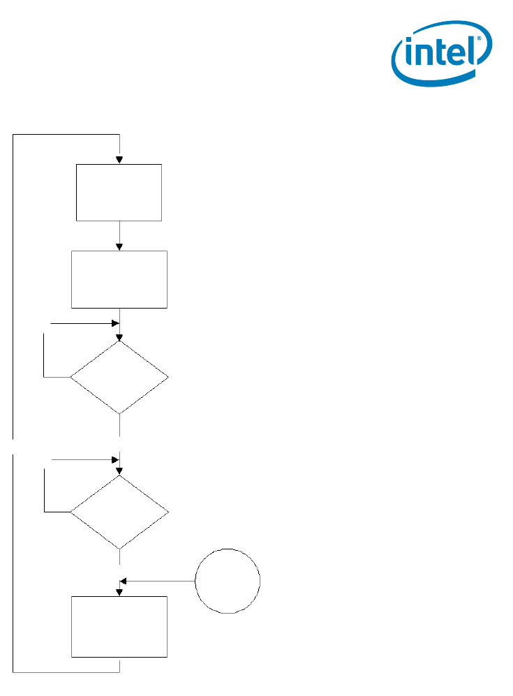
Interrupt Moderation — Intel® 82575EB Gigabit Ethernet Controller
324632-003 Intel® 82575EB Gigabit Ethernet Controller
Revision: 2.1 Software Developer’s Manual and EEPROM Guide
January 2011 167
Figure 20. Interrupt Throttle Flow Diagram
For cases where the 82575 is connected to a small number of clients, it is desirable to initiate the
interrupt as soon as possible with minimum latency. For these cases, when the EITR counter counts
down to zero and no interrupt event has happened, then the EITR counter is not reset but stays at zero.
Therefore, the next interrupt event triggers an immediate interrupt (see Figure 21 and Figure 22).
Yes
No
No
Yes
Start Count
Load Counter
with Interval
Down
Counter = 0
?
Interrupt
Active
?
Assert Interrupt
Counter
Written to
0
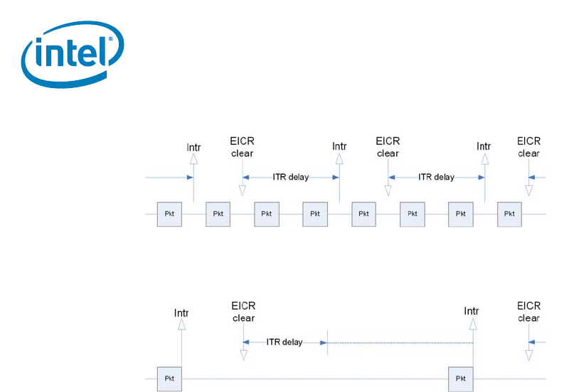
Intel® 82575EB Gigabit Ethernet Controller — Clearing Interrupt Causes
Intel® 82575EB Gigabit Ethernet Controller 324632-003
Software Developer’s Manual and EEPROM Guide Revision: 2.1
168 January 2011
Figure 21. Case A: Heavy Load, Interrupts Moderated
Figure 22. Case B: Light Load, Interrupts Immediately on Packet Receive
5.15 Clearing Interrupt Causes
The 82575 has three available methods for clearing the EICR bits: auto-clear, clear-on-write, and clear-
on-read. Note that ICR bits can only be cleared with clear-on-write or clear-on-read.
5.15.1 Auto-Clear
In systems that support MSI-X, the interrupt vector enables the interrupt service routine to know the
interrupt cause without reading EICR. With interrupt moderation active, software loads from spurious
interrupts is minimized. In this case, the software overhead of a I/O read or write can be avoided by
setting appropriate EICR bits to auto-clear mode by setting the corresponding bits in the EIAC.
When auto-clear is enabled for a interrupt cause, the EICR bit is set when a cause event occurs. When
the EITR counter reaches zero, the MSI-X message is sent on to the PCIe* interface. Afterwards, the
EICR bit is cleared and enabled to be set by a new cause event. The vector in the MSI-X message
signals software the cause of the interrupt to be serviced.
It is possible that in the time after the EICR bit is cleared and the interrupt service routine services the
cause, for example checking the transmit and receive queues, that another cause event occurs that is
then serviced by this ISR call, yet the EICR bit remains set. This results in a spurious interrupt.
Software can detect this case, for example if there are no entries that require service in the transmit
and receive queues, and exit knowing that the interrupt has been automatically cleared. The use of
interrupt moderations through the EITR register limits the extra software overhead that can be caused
by these spurious interrupts.

Write to Clear — Intel® 82575EB Gigabit Ethernet Controller
324632-003 Intel® 82575EB Gigabit Ethernet Controller
Revision: 2.1 Software Developer’s Manual and EEPROM Guide
January 2011 169
5.15.2 Write to Clear
In the case where the software device driver wants to configure itself in MSI-X mode to not use the
auto-clear feature, it might clear the EICR bits by writing to the EICR register. Any bits written with a 1b
is cleared. Any bits written with a 0b remain unchanged.
5.15.3 Read to Clear
The EICR and ICR registers are cleared on a read.
Note: The software device driver should never do a read-to-clear of the EICR when in MSI-X
mode, since this can clear interrupt cause events which are processed by a different
interrupt handler (assuming multiple vectors).
5.16 Dynamic Interrupt Moderation
There are some types of network traffic for which latency is a critical issue. For these types of traffic,
interrupt moderation hurts performance by increasing latency between when a packet is received by
hardware and when it is indicated to the host operating system. This traffic can be identified by the TCP
port value in conjunction with control bits, size and VLAN priority.
The 82575 implements an eight-entry, software programmable, table of TCP ports and eight registers
with control bits filter and size threshold. In addition, a dedicated register enables setting of a VLAN
priority threshold. If a packet is received on one of these TCP ports, and the conditions set by the
register fit to the packet, hardware should interrupt immediately, overriding the interrupt moderation
by the EITR counter.
A Port Enabling bit allows enabling or disabling of a specific port for this purpose; VLAN priority filtering
allows issuing of immediate interrupt.
The logic of the dynamic interrupt moderation is as follows:
• There are eight port filters. Each filter checks the value of incoming packets TCP port, size, and
control bits against values stored in the filter's register. Each parameter can be bypassed (or via a
wildcard). Each filter can be enabled or disabled. If one of the filters detects an adequate packet, an
immediate interrupt is issued.
• When VLAN priority filtering is enabled, VLAN packets trigger an immediate interrupt when the
VLAN priority is equal to or above the VLAN priority threshold. This is regardless of the status of the
port filters.
Note: EITR is reset to 0b following a dynamic interrupt.
Immediate interrupts are available only when using advanced receive descriptors as
opposed to legacy descriptors.

Intel® 82575EB Gigabit Ethernet Controller — TCP Timer Interrupt
Intel® 82575EB Gigabit Ethernet Controller 324632-003
Software Developer’s Manual and EEPROM Guide Revision: 2.1
170 January 2011
5.16.1 TCP Timer Interrupt
In order to implement TCP timers for I/OAT 2, software needs to take action periodically (every 10
milliseconds). The software device driver must rely on software-based timers, whose granularity can
change from platform to platform. This software timer generates a software Network Interface Card
(NIC) interrupt, which then enables the software device driver to perform timer functions as part of its
usual DPC. Note that the timer interval is system-specific.
It would be more accurate and more efficient for this periodic timer to be implemented in hardware.
The software device driver could program a timeout value (usual value of 10 ms), and each time the
timer expires, hardware sets a specific bit in the EICR. When an interrupt occurs (due to normal
interrupt moderation schemes), software reads the EICR and discovers that it needs to process timer
events during that DPC.
The timeout should be programmable by the software device driver, and it should be able to disable the
timer interrupt if it is not needed.
A stand-alone down-counter is implemented. with an interrupt issued each time the value of the
counter is zero.
Software is responsible for setting the initial value for the timer in the Duration field. Kick-starting is
done by writing a 1b to the Kick Start bit.
Following kick-starting, an internal counter is set to the value defined by the Duration field. Afterwards,
the counter is decreased by one each millisecond. When the counter reaches zero, an interrupt is
issued. The counter re-starts counting from its initial value if the Loop field is set.
5.17 Memory Error Correction and Detection
The 82575 internal memories are protected by error correcting code that might correct memory errors
and detect uncorrectable error. Correctable errors are silently corrected and are counted in the
PBECCSTS.Corr_err_cnt, RDHESTS.Corr_err_cnt or TDHESTS.Corr_err_cnt fields according to the
memory in which the error was found.
Uncorrectable errors are counted in the PBECCSTS.Uncorr_err_cnt, RDHESTS.Uncorr_err_cnt or
TDHESTS.Uncorr_err_cnt fields according to the memory in which the error was found. The 82575
reacts to uncorrectable error detection according to the location in which the error was found:
• If the error was detected in a receive packet data, the packet is sent to the host with the RXE bit set
in the receive descriptor. This packet should be discarded by the host.
• If the error was detected in a transmit packet data, the packet is sent to the network with a wrong
FCS so that the link partner can discard it.
• If the error was detected in the descriptors attached to receive or transmit packets or in the
descriptor handler cache memory, the consistency of the receive/transmit flow cannot be
guaranteed. In this case, the flow in which the error was detected is stopped and an interrupt is
generated indicating the location of the detected error. The flow stop can be released only by a
software reset (CTRL.RST). The interrupt causes used to indicate an unrecoverable error are
ICR[25:22] according to the location of the error.
Enabling the reaction mechanism of the 82575 to uncorrectable errors is done using the
CTRL_EXT.MEHE bit.

PCIe* Local Bus Interface — Intel® 82575EB Gigabit Ethernet Controller
324632-003 Intel® 82575EB Gigabit Ethernet Controller
Revision: 2.1 Software Developer’s Manual and EEPROM Guide
January 2011 173
6.0 PCIe* Local Bus Interface
This section describes the software interface and some related hardware aspects of PCIe* in regard to
the 82575.
6.1 General Functionality
•Native/Legacy Functionality. All 82575 PCI functions are native PCIe* functions.
•Locked Transactions. The 82575 does not support locked requests as a target or master.
•End to End CRC. This is not supported by the 82575.
6.1.1 Message Handling (Receive Side)
Message packets are special packets that carry message code. The upstream device transmits special
messages to the 82575 by using this mechanism. The transaction layer decodes the message code and
responds accordingly.
6.1.2 Message Handling (Transmit Side)
The transaction layer is also responsible for transmitting specific messages to report internal and
external events such as interrupts and power management events.
Table 50. Supported Messages on the Receive Side
Message Code
[7:0] Routing r2r1r0 Name Device Response
14h 100 PM_Active_State_NAK Stop ASPM L1 negotiation and go
back to L0
19h 011 PME_Turn_Off Send PME_to_Ack and start L2
negotiation
50h 100 Slot power limited support (one Dword) Silently drop
7Eh 010,011,100 Vendor_Defined Type 0 (no data) Unsupported request
7Eh 010,011,100 Vendor_Defined Type 0 (data) Unsupported request
7Fh 010,011,100 Vendor_Defined Type 1 (no data) Silently drop
7Fh 010,011,100 Vendor_Defined Type 1 (data) Silently drop
00h 011 Unlock Silently drop

Intel® 82575EB Gigabit Ethernet Controller — Data Alignment
Intel® 82575EB Gigabit Ethernet Controller 324632-003
Software Developer’s Manual and EEPROM Guide Revision: 2.1
174 January 2011
6.1.3 Data Alignment
6.1.3.1 4 KB Boundary
Requests must not specify an address/length combination causing memory space access to cross a 4
KB boundary. It is the hardware responsibility to break requests into 4 KB aligned requests if required.
This does not create any software requirement. However, if software allocates a buffer across the 4 KB
boundary, hardware issues multiple requests for the buffer. Software should align buffers to the 4 KB
boundary in cases where it improves performance.
The general rules for packet alignment are as follows. Note that these apply to all 82575 requests
(read/write, snoop and no snoop):
• The length of a single request does not exceed the PCIe* limit of MAX_PAYLOAD_SIZE for write and
MAX_READ_REQ for read
• The length of a single request does not exceed 82575’s internal limitations of 256 bytes for write
and 512 bytes for read.
• A single request does not span across different memory pages as noted by the 4 KB boundary.
If a request can be sent as a single PCIe* packet and still meet the general rules for packet alignment,
then it is not broken at the cacheline boundary but rather sent as a single packet However, if the
general rules require that the request is broken into two or more packets, then the request is broken at
cacheline boundary.
6.1.4 Transaction Attributes
6.1.4.1 Traffic Class and Virtual Channels
The 82575 only supports Traffic Class 0 (default) and Virtual Channel 0 (default).
Table 51. Supported Messages on the Transmit Side
Message Code [7:0] Routing r2r1r0 Description
20h 100 Assert INT A
21h 100 Assert INT B
22h 100 Assert INT C
23h 100 Assert INT D
24h 100 De-assert INT A
25h 100 De-assert INT B
26h 100 De-assert INT C
27h 100 De-assert INT D
30h 000 ERR_COR
31h 000 ERR_NONFATAL
33h 000 ERR_FATAL
18h 000 PM_PME
1Bh 101 PME_to_Ack

Transaction Attributes — Intel® 82575EB Gigabit Ethernet Controller
324632-003 Intel® 82575EB Gigabit Ethernet Controller
Revision: 2.1 Software Developer’s Manual and EEPROM Guide
January 2011 175
6.1.4.2 Relaxed Ordering
The 82575 takes advantage of the relaxed ordering rules of the PCIe* Specification.
Relaxed ordering can be used in conjunction with the no snoop attribute to allow the memory controller
to advance non-snoop writes ahead of earlier snooped writes.
Relaxed ordering is enabled in the 82575 by clearing the RO_DIS bit in the CTRL_EXT register. The
actual setting of relaxed ordering is done for LAN traffic by the host through the DCA registers.
Note: The 82575 cannot perform relax ordering for descriptor writes or an MSI write.
6.1.4.3 Snoop Not Required
The 82575 can be configured to set the Snoop Not Required attribute bit for master data writes.
System logic can provide a separate path into system memory for non-coherent traffic. The non-
coherent path to system memory provides a higher, more uniform bandwidth for write requests.
Note: The Snoop Not Required attribute does not alter transaction ordering. Therefore, to achieve
maximum benefit from snoop not required transactions, it is advisable to also set the
relaxed ordering attribute. This assumes that system logic supports both the snoop not
required and relaxed ordering attributes.
No snoop is enabled in the 82575 by clearing the NS_DIS bit in the CTRL_EXT register. The actual
setting of no snoop is done for LAN traffic by the host through the DCA registers.
6.1.4.3.1 No Snoop and Relaxed Ordering for LAN Traffic
Software configures non-snoop and relax order attributes for each queue and each type of transaction
by setting the respective bits in the DCA_RXCTRL and TCA_TXCTRL registers.
Table 52 lists the default behavior for the No Snoop and Relaxed Ordering bits for LAN traffic when I/
OAT 2 is enabled.
Table 52. LAN Traffic Attributes
Note: Rx payload no snoop is also conditioned by the NSE bit in the Receive descriptor.
6.1.4.3.2 No Snoop Option for Payload
Transaction No Snoop Default Relaxed Ordering
Default Comments
Rx Descriptor Read N Y
Rx Descriptor Write Back N N RO must never be
used for this traffic
Rx Data Write Y Y See note and section
below
Rx Replicated Header N Y
Tx Descriptor Read N Y
Tx Descriptor Write Back N Y
Tx Data Write N Y

Intel® 82575EB Gigabit Ethernet Controller — Flow Control
Intel® 82575EB Gigabit Ethernet Controller 324632-003
Software Developer’s Manual and EEPROM Guide Revision: 2.1
176 January 2011
Under certain conditions that occur when I/OAT is enabled, software knows that it is safe to transfer a
new packet into a certain buffer without snooping on the front-side bus. This scenario occurs when
software is posting a receive buffer to hardware that the CPU has not accessed since the last time it was
owned by hardware. This might happen if the data was transferred to an application buffer by the data
movement engine. As such, software should be able to set a bit in the receive descriptor indicating that
the 82575 should perform a no snoop transfer when it eventually writes a packet to this buffer.
When a non-snoop transaction is activated, the TLP header has a non-snoop attribute in the Transaction
Descriptor field. This is triggered by the NSE bit in the Receive descriptor.
6.2 Flow Control
6.2.1 Flow Control Rules
The 82575 implements only the Default Virtual Channel (VC0). A single set of credits is maintained for
VC0.
The flow control update rules are as follows:
• The 82575 maintains two credits for Non-Posted Request Data at any given time. The controller
increments the credit by one after the credit is consumed and sends an UpdateFC packet as soon as
possible. UpdateFC packets are scheduled immediately after a resource is available.
• The 82575 provides two credits for Posted Request Header. For example, two credits are given for
two concurrent target writes and two credits for Non-Posted Request Header (two concurrent target
reads). UpdateFC packets are scheduled immediately after a resource is available.
• The 82575 follows the PCIe* recommendations for frequency of UpdateFC FCPs.
6.2.2 Upstream Flow Control Tracking
The 82575 issues a master transaction only when the required flow control credits are available. Credits
are tracked for posted, non-posted and completions. The later operates against a switch.
Table 53. Flow Control Credit Allocation
Credit Type Operations Number of Credits
Posted Request Header (PH) Target Write (1 unit)
Message (1 unit)
2 units (allowing concurrent
accesses to both LAN ports)
Posted Request Data (PD) Target Write (length per 16 bytes =
1)
Message (1 unit)
MAX_PAYLOAD_SIZE/16
Non-Posted Request Header
(NPH)
Target Read (1 unit)
Configuration Read (1 unit)
Configuration Write (1 unit)
2 units (allowing concurrent
target accesses to both LAN
ports)
Non-Posted Request Data (NPD) Configuration Write (1 unit) 2 units
Completion Header (CPLH) Read Completion (not applicable) Infinite (accepted immediately)
Completion Data (CPLD) Read Completion (not applicable) Infinite (accepted immediately)

Flow Control Update Frequency — Intel® 82575EB Gigabit Ethernet Controller
324632-003 Intel® 82575EB Gigabit Ethernet Controller
Revision: 2.1 Software Developer’s Manual and EEPROM Guide
January 2011 177
6.2.3 Flow Control Update Frequency
In any case, UpdateFC packets are scheduled immediately after a resource is available. When the Link
is in the L0 or L0s link state, Update FCPs for each enabled type of non-infinite flow control credit must
be scheduled for transmission at least once every 30 μs (-0% or +50%), except when the extended
synchronize bit of the control link register is set. In this case, the limit is 120 μs (-0% or +50%).
6.2.4 Flow Control Timeout Mechanism
The 82575 implements the optional flow control update timeout mechanism. This mechanism is
activated when the link is in L0 or L0s link state. It uses a timer with a limit of 200 μs (0% or +50%),
where the timer is reset by the receipt of any DLLP.
When the timer expires, the mechanism instructs the PHY to retrain the link through the LTSSM
recovery state.
6.2.5 Error Forwarding
If a TLP is received with an error forwarding trailer, the packet is dropped and is not delivered to its
destination.
System logic is expected to trigger a system level interrupt to inform the operating system of the
problem. The operating system has the ability to stop the process associated with the transaction, re-
allocate memory instead of the faulty area, etc.
6.3 Host Interface
6.3.1 Tag IDs
PCIe* device numbers identify logical devices within the physical device. The 82575 implements a
single logical device with up to two separate PCI functions: LAN 0 and LAN 1. The device number is
captured from each type 0 configuration write transaction.
Each of the PCIe* functions interfaces with the PCIe* unit through one or more clients. A client ID
identifies the client and is included in the tag field of the PCIe* packet header. Completions always carry
the tag value included in the request to allow routing of the completion to the appropriate client.
Tag IDs are allocated differently for read and write.
• For reads, Table 54 lists the Tag ID allocation. The Tag ID is interpreted by hardware in order to
forward the read data to the required device.
• For writes, Table 55 and Table 56 list the Tag ID allocation when DCA mode is not active. Unlike
reads, the values are for debug only enabling tracing of requests through the system. When in DCA
mode, the Tag IDs are replaced by the adequate DCA bits.
Note: Only five low bits of tags are usable because the configuration of the Extended Tag Field
Enable bit in the configuration space Device Control register (8h) depends on the operating
system and is not predictable.

Intel® 82575EB Gigabit Ethernet Controller — Tag IDs
Intel® 82575EB Gigabit Ethernet Controller 324632-003
Software Developer’s Manual and EEPROM Guide Revision: 2.1
178 January 2011
Table 54 lists the tag IDs in read transactions.
Since DCA is implemented differently in data movement engine 1 and in data movement engine 2
platforms, the tag IDs are different as well.
DCA mode (data movement engine 1 and 2) is done by setting the DCA_Mode bit in the DCA Mode
register.
DCA itself is enabled or disabled by setting the DCA_Dis bit in the GCR register.
Table 55. Tag IDs in Write Transactions (Data Movement Engine 1)
Table 54. Assignment of Tag IDs
Tag ID Description
00h Reserved
01h Descriptor Rx
03h:02h Reserved
04h Descriptor Tx
07h:05h Reserved
08h Data Request 0
09h Data Request 1
0Ah Data Request 2
0Bh Data Request 3
10h Management
11h Message Unit
12h:1Fh Reserved
Tag ID Description DCA
00h Management Disabled
01h Descriptors, data, WB tail for CPU ID 0 Enabled
02h WB descriptor Tx / WB tail Disabled
03h Descriptors, data, WB tail for CPU ID 1 Enabled
04h WB descriptor Rx Disabled
05h Descriptors, data, WB tail for CPU ID 2 Enabled
06h Write data Disabled
07h Descriptors, data, WB tail for CPU ID 3 Enabled
08h Reserved -
09h Descriptors, data, WB tail for CPU ID 4 Enabled
0Ah Reserved Disabled
0Bh Descriptors, data, WB tail for CPU ID 5 Enabled
0Ch Reserved Disabled
0Dh Descriptors, data, WB tail for CPU ID 6 Enabled

Tag IDs — Intel® 82575EB Gigabit Ethernet Controller
324632-003 Intel® 82575EB Gigabit Ethernet Controller
Revision: 2.1 Software Developer’s Manual and EEPROM Guide
January 2011 179
Tag ID Description DCA
0Eh Reserved Disabled
0Fh Descriptors, data, WB tail for CPU ID 7 Enabled
1Bh:10h Reserved -
1Ch Reserved Disabled
1Dh Reserved Enabled
1Eh MSI,MSI-X Disabled
1Fh Messages Enabled

Intel® 82575EB Gigabit Ethernet Controller — Tag IDs
Intel® 82575EB Gigabit Ethernet Controller 324632-003
Software Developer’s Manual and EEPROM Guide Revision: 2.1
180 January 2011
Table 56. Tag IDs in Write Transactions (Data Movement Engine 2)
Note: While in data movement engine 2 mode, if DCA is not enabled in the platform then the Tag
Tag ID Description DCA
00h All (no hint) Enabled
01h Descriptors, data, WB tail for CPU ID 1 Enabled
02h Descriptors, data, WB tail for CPU ID 2 Enabled
03h Descriptors, data, WB tail for CPU ID 3 Enabled
04h Descriptors, data, WB tail for CPU ID 4 Enabled
05h Descriptors, data, WB tail for CPU ID 5 Enabled
06h Descriptors, data, WB tail for CPU ID 6 Enabled
07h Descriptors, data, WB tail for CPU ID 7 Enabled
08h Descriptors, data, WB tail for CPU ID 8 Enabled
09h Descriptors, data, WB tail for CPU ID 9 Enabled
0Ah Descriptors, data, WB tail for CPU ID 0A Enabled
0Bh Descriptors, data, WB tail for CPU ID 0B Enabled
0Ch Descriptors, data, WB tail for CPU ID 0C Enabled
0Dh Descriptors, data, WB tail for CPU ID 0D Enabled
0Eh Descriptors, data, WB tail for CPU ID 0E Enabled
0Fh Descriptors, data, WB tail for CPU ID 0F Enabled
10h Descriptors, data, WB tail for CPU ID 10 Enabled
11h Descriptors, data, WB tail for CPU ID 11 Enabled
12h Descriptors, data, WB tail for CPU ID 12 Enabled
13h Descriptors, data, WB tail for CPU ID 13 Enabled
14h Descriptors, data, WB tail for CPU ID 14 Enabled
15h Descriptors, data, WB tail for CPU ID 15 Enabled
16h Descriptors, data, WB tail for CPU ID 16 Enabled
17h Descriptors, data, WB tail for CPU ID 17 Enabled
18h Descriptors, data, WB tail for CPU ID 18 Enabled
19h Descriptors, data, WB tail for CPU ID 19 Enabled
1Ah Descriptors, data, WB tail for CPU ID 1A Enabled
1Bh Descriptors, data, WB tail for CPU ID 1B Enabled
1Ch Descriptors, data, WB tail for CPU ID 1C Enabled
1Dh Descriptors, data, WB tail for CPU ID 1D Enabled
1Eh Descriptors, data, WB tail for CPU ID 1E Enabled
1Fh Descriptors, data, WB tail for CPU ID 1F Disabled
Completion Timeout Mechanism — Intel® 82575EB Gigabit Ethernet Controller
324632-003 Intel® 82575EB Gigabit Ethernet Controller
Revision: 2.1 Software Developer’s Manual and EEPROM Guide
January 2011 181
IDs are as in data movement engine 1 mode. When in data movement engine 2 mode,
messages and MSI/MSI-X write requests are sent with a hint tag of 1Fh.
6.3.2 Completion Timeout Mechanism
The completion timeout mechanism is activated for each request that requires one or more completions
when the request is transmitted. Revision 1.1 of the PCI specification requires:
• Completion Timeout timer should not expire in less than 10 ms.
• Completion Timeout timer must expire if a request is not completed in 50 ms.
However, some platforms experience completion latencies that are longer than 50 ms, in some cases up
to seconds. The 82575 provides a programmable range for the completion timeout as well as the ability
to disable the completion timeout altogether. The new capability structure is assigned a PCIe* capability
structure version of 2h.
The 82575 controls the following aspects of completion timeout:
• Disabling or enabling completion timeout
• Disabling or enabling resending a request on completion timeout
• A programmable range of timeout values
Programming the behavior of completion timeout is done differently whether capability structure
version 1h is enabled or capability structure version 2h. Table 57 lists the behavior for both cases.
Table 57. Completion Timeout Programming
Completion Timeout Enable:
• Version = 1h- Loaded from the Completion Timeout Disable bit in the EEPROM into the
Completion_Timeout_Disable bit in the PCIe* Control register (GCR). The default is completion
timeout enabled.
• Version = 2h - Programmed through PCI configuration. Visible through the
Completion_Timeout_Disable bit in the PCIe* Control register (GCR). The default is completion
timeout enabled.
Resend Request Enable:
• The Completion Timeout Resend EEPROM bit, loaded in the Completion_Timeout_Resend bit in the
PCIe* Control register (GCR), enables resending the request (applies only when completion timeout
is enabled). The default is to resend a request that timed out.
Completion Timeout Period:
• Version = 1h.- Loaded from the Completion Timeout Value field in the EEPROM to the _
Completion_Timeout_Value bits in the PCIe* Control register (GCR).
Capability Capability Structure Version = 1h Capability Structure Version = 2h
Completion timeout
enabling
Loaded from EEPROM into CSR bit Controlled through PCI configuration. Visible
through read-only CSR bit
Resend request
enable
Loaded from EEPROM into CSR bit Loaded from EEPROM into read-only CSR bit
Completion Timeout
period
Loaded from EEPROM into CSR bit Controlled through PCI configuration. Visible
through read-only CSR bit

Intel® 82575EB Gigabit Ethernet Controller — Error Events and Error Reporting
Intel® 82575EB Gigabit Ethernet Controller 324632-003
Software Developer’s Manual and EEPROM Guide Revision: 2.1
182 January 2011
• Version = 2h - Programmed through PCI configuration. Visible through the
Completion_Timeout_Value bits in the PCIe* Control register (GCR).
System software programs a range (one of 9 possible ranges that sub-divide the four ranges) into the
PCI configuration register. The supported sub-ranges are:
• 50 s to 50 ms (default).
• 50 s to 100 s
• 1 ms to 10 ms
• 16 ms to 55 ms
• 65 ms to 210 ms
• 260 ms to 900 ms
• 1 s to 3.5 s
• 4 s to 13 s
• 17 s to 64 s
A memory read request for which there are multiple completions are considered completed only when
all completions have been received by the requester. If some, but not all, requested data is returned
before the completion timeout timer expires, the requestor is permitted to keep or to discard the data
that was returned prior to timer expiration.
6.4 Error Events and Error Reporting
The PCIe* Specification defines two error reporting paradigms:
• Baseline error reporting capability.
• Advanced error reporting capability.
The baseline error reporting capabilities are required of all PCIe* devices and define the minimum error
reporting requirements. The advanced error reporting capability is defined for more robust error
reporting and is implemented with a specific PCIe* capability structure. Both mechanisms are
supported by the 82575.
Also, the SERR# enable and the parity error bits from the legacy command register take part in the
error reporting and logging mechanism.
6.4.1 Error Events
Table 58 lists the error events identified by the 82575 and its response. The PCIe* Specification can be
consulted for the effect on the PCI Status register.
Table 58. Response and Reporting of Error Events
Error Types Error Events Default Severity Action
Physical Layer Errors
Receiver Error • 8b/10b decode errors.
• Packet framing error.
Correctable.
Send ERR_CORR.
TLP Initiate Nak; drop data.
DLLP Drop.
Data Link Errors

Error Events — Intel® 82575EB Gigabit Ethernet Controller
324632-003 Intel® 82575EB Gigabit Ethernet Controller
Revision: 2.1 Software Developer’s Manual and EEPROM Guide
January 2011 183
Bad TLP • Bad CRC.
• Illegal EDB.
• Wrong sequence number.
Correctable.
Send ERR_CORR.
TLP Initiate Nak; drop data.
Bad DLLP Bad CRC. Correctable.
Send ERR_CORR.
DLLP Drop.
Replay Timer
Timeout
Replay timer expiration. Correctable.
Send ERR_CORR.
Follow LL rules.
Replay Number
Rollover
Replay number rollover. Correctable.
Send ERR_CORR.
Follow LL rules.
Data Link Layer
Protocol Error
Received ACK/NACK not
corresponding to any TLP.
Uncorrectable.
Send ERR_FATAL.
Follow LL rules.
TLP Errors
Poisoned TLP
Received
TLP with error forwarding. Uncorrectable.
ERR_NONFATAL.
Log header.
A poisoned completion is ignored
and the request can be retried
after timeout. If enabled, the
error is reported.
Unsupported
Request (UR)
• Wrong configuration access.
• MRdLk.
• Configuration request type1.
• Unsupported vendor. Defined
type 0 message:
• Invalid MSG code.
• Unsupported TLP type.
• Wrong function number.
• Wrong traffic class or virtual
channel.
• Received target access with
data size larger than 64 bits.
• Received TLP outside address
range.
Uncorrectable.
ERR_NONFATAL.
Log header.
Send completion with UR.
Completion
Timeout
Completion Timeout timer
expired.
Uncorrectable.
ERR_NONFATAL.
Send the read request again
Completer Abort
(CA)
Attempts to write to the FLASH
device when writes are disabled
(FWE = 10b).
Uncorrectable.
ERR_NONFATAL.
Log header.
Send completion with CA.
Unexpected
Completion
Received completion without a
request for it (tag, ID, etc.).
Uncorrectable.
ERR_NONFATAL.
Log header.
Discard TLP.
Receiver Overflow Received TLP beyond allocated
credits.
Uncorrectable.
ERR_FATAL.
Receiver behavior is undefined.
Flow Control
Protocol Error
• Minimum initial flow control
advertisements.
• Flow control update for
infinite credit advertisement.
Uncorrectable.
ERR_FATAL.
Receiver behavior is undefined.
Table 58. Response and Reporting of Error Events
Error Types Error Events Default Severity Action

Intel® 82575EB Gigabit Ethernet Controller — Error Pollution
Intel® 82575EB Gigabit Ethernet Controller 324632-003
Software Developer’s Manual and EEPROM Guide Revision: 2.1
184 January 2011
6.4.2 Error Pollution
Error pollution can occur if error conditions for a given transaction are not isolated to the error’s first
occurrence. If the Physical Layer detects and reports a Receiver Error, to avoid having this error
propagate and cause subsequent errors at upper layers, the same packet is not signaled at the Data
Link or Transaction layers.
Similarly, when the Data Link Layer detects an error, subsequent errors, which occur for the same
packet, are not signaled at the Transaction Layer.
6.4.3 Unsuccessful Completion Status
A completion with an unsuccessful completion status is dropped and not delivered to its destination.
The request that corresponds to the unsuccessful completion is retried by sending a new request for the
undeliverable data.
6.4.4 Error Reporting Changes
The Revision 1.1 PCI specification defines two changes to advanced error reporting. A (new) Role-
Based Error Reporting bit in the Device Capabilities register is set to 1b to indicate that these changes
are supported by the 82575.
1. Setting the SERR# Enable bit in the PCI Command register also enables UR reporting (in the same
manner that the SERR# Enable bit enables reporting of correctable and uncorrectable errors). The
SSERR# Enable bit overrides the UR Error Reporting Enable bit in the PCI Express Device Control
register.
Malformed TLP
(MP)
• Data payload exceeds
maximum payload size.
• Received TLP data size does
not match length field.
• TD field value does not
correspond with the observed
size.
• Byte enables violations.
• PM messages that do not use
TC0.
• Usage of unsupported VC.
Uncorrectable.
ERR_FATAL.
Log header.
Packet dropped. Free flow control
credits.
Completion with
Unsuccessful
Completion Status
No action (already done by
originator of completion).
Free FC credits.
Byte count
integrity
When byte count isn't compatible
with the length field and the
actual expected completion
length. For example, length field
is 10 (in Dword), actual length is
40, but the byte count field that
indicates how many bytes are
still expected is smaller than 40,
which is not reasonable.
Uncorrectable.
ERR_FATAL
The 82575 doesn’t check for this
error and accepts these packets.
This might cause a completion
timeout condition.
Table 58. Response and Reporting of Error Events
Error Types Error Events Default Severity Action

Link Layer — Intel® 82575EB Gigabit Ethernet Controller
324632-003 Intel® 82575EB Gigabit Ethernet Controller
Revision: 2.1 Software Developer’s Manual and EEPROM Guide
January 2011 185
2. Changes in the response to some Uncorrectable Non-Fatal errors detected in non-posted requests
to the 82575 called Advisory Non-fatal Error cases. For each of the errors listed, the following
behavior is defined:
a. The Advisory Non-Fatal Error Status bit is set in the Correctable Error Status register to indicate
the occurrence of the advisory error, and the Advisory Non-Fatal Error Mask corresponding bit in
the Correctable Error Mask register is checked to determine whether to proceed further with
logging and signaling.
b. If the Advisory Non-Fatal Error Mask bit is clear, logging proceeds by setting the corresponding
bit in the Uncorrectable Error Status register, based upon the specific uncorrectable error that is
being reported as an advisory error. If the corresponding uncorrectable error bit in the
Uncorrectable Error Mask register is clear, the First Error Pointer and Header Log registers are
updated to log the error, assuming they are not still occupied by a previously unserviceable error.
c. An ERR_COR Message is sent if the Correctable Error Reporting Enable bit is set in the Device
Control register. An ERROR_NONFATAL message is not sent for this error.
The following Uncorrectable Non-Fatal errors are considered as Advisory Non-fatal Errors:
• A Completion with an Unsupported Request or Completer Abort (UR/CA) Status that signals an
uncorrectable error for a Non-Posted Request. If the severity of the UR/CA error is non-fatal, the
Completer must handle this case as an Advisory Non-Fatal Error.
• When the Requester of a Non-Posted Request times out while waiting for the associated
Completion, the Requester is permitted to attempt to recover from the error by issuing a separate
subsequent Request or to signal the error without attempting recovery. The Requester is permitted
to attempt recovery zero, one, or multiple (finite) times, but must signal the error (if enabled) with
an uncorrectable error Message if no further recovery attempt is made. If the severity of the
Completion Timeout is non-fatal, and the Requester elects to attempt recovery by issuing a new
request, the Requester must first handle the current error case as an Advisory Non-Fatal Error.
• When a Receiver receives an unexpected Completion and the severity of the Unexpected
Completion error is non-fatal, the Receiver must handle this case as an Advisory Non-Fatal Error.
6.5 Link Layer
6.5.1 ACK/NAK Scheme
The 82575 supports two alternative schemes for ACK/NAK rate:
1. ACK/NAK is scheduled for transmission according to timeouts specified in the LTIV register.
2. ACK/NAK is scheduled for transmission according to time-outs specified in the PCIe* Specification.
The ACK/NAK scheme bit loaded from the EEPROM determines which of the two schemes is used.
6.5.2 Supported DLLPs
The following DLLPs are supported by the 82575 as a receiver.
Table 59. DLLPs Received
Ack
Nak
PM_Request_Ack
Intel® 82575EB Gigabit Ethernet Controller — Transmit EDB Nullifying
Intel® 82575EB Gigabit Ethernet Controller 324632-003
Software Developer’s Manual and EEPROM Guide Revision: 2.1
186 January 2011
The following DLLPs are supported by the 82575 as a transmitter.
6.5.3 Transmit EDB Nullifying
In case of a retrain, there is a need to guarantee that no abrupt termination of the transmit packet
occurs. For this reason, early termination of the transmitted packet is possible. This is accomplished by
appending EDB to the packet.
6.6 Physical Layer
6.6.1 Link Width
The 82575 supports a maximum link width of x4, x2, or x1 as determined by the minimum of:
• The PCIEPert SKU fuse
• The EEPROM Lane_Width field in PCIe* Initialization Configuration 3 word
InitFC1-P v2v1v0 = 000
InitFC1-NP v2v1v0 = 000
InitFC1-Cpl v2v1v0 = 000
InitFC2-P v2v1v0 = 000
InitFC2-NP v2v1v0 = 000
InitFC2-Cpl v2v1v0 = 000
UpdateFC-P v2v1v0 = 000
UpdateFC-NP v2v1v0 = 000
UpdateFC-Cpl v2v1v0 = 000
Table 60. DLLPs Initiated
Ack
Nak
PM_Enter_L1
PM_Enter_L23
PM_Active_State_Request_L1
InitFC1-P v2v1v0 = 000
InitFC1-NP v2v1v0 = 000
InitFC1-Cpl v2v1v0 = 000
InitFC2-P v2v1v0 = 000
InitFC2-NP v2v1v0 = 000
InitFC2-Cpl1
1. UpdateFC-Cpl is not transmitted due to the infinite FC-CPL allocation.
v2v1v0 = 000
UpdateFC-P v2v1v0 = 000
UpdateFC-NP v2v1v0 = 000
Table 59. DLLPs Received

Link Width — Intel® 82575EB Gigabit Ethernet Controller
324632-003 Intel® 82575EB Gigabit Ethernet Controller
Revision: 2.1 Software Developer’s Manual and EEPROM Guide
January 2011 187
The max link width is loaded into the Maximum Link Width field of the PCIe* Capability register
(LCAP[11:6]). The hardware default is the x4 link.
During link configuration, the platform and the 82575 negotiate on a common link width. The link width
must be one of the supported PCIe* link widths (1x, 2x, 4x), such that:
• If Maximum Link Width = x4, then the 82575 negotiates to either x4, x2 or x1
• If Maximum Link Width = x2, then the 82575 negotiates to either x2 or x1
• If Maximum Link Width = x1, then the 82575 only negotiates to x1
6.6.1.1 Polarity Inversion
If polarity inversion is detected, the Receiver must invert the received data.
During the training sequence, the Receiver looks at Symbols 6-15 of TS1 and TS2 as the indicator of
Lane polarity inversion (D+ and D- are swapped). If Lane polarity inversion occurs, the TS1 Symbols 6-
15 received are D21.5 as opposed to the expected D10.2. Similarly, if Lane polarity inversion occurs,
Symbols 6-15 of the TS2 ordered set are D26.5 as opposed to the expected D5.2. This provides the
clear indication of Lane polarity inversion.
6.6.1.2 L0s Exit latency
The number of FTS sequences (N_FTS) sent during L0s exit, is loaded from the EEPROM.
6.6.1.3 Lane-to-Lane De-Skew
A multi-lane link can have many sources of lane to lane skew. Although symbols are transmitted
simultaneously on all lanes, they cannot be expected to arrive at the receiver without lane-to-lane
skew. The lane-to-lane skew may include components, which are less than a bit time, bit time units
(400 ps for 2.5 Gb), or full symbol time units (4 ns) of skew caused by the retiming repeaters’ insert/
delete operations. Receivers use TS1 or TS2 or Skip ordered sets (SOS) to perform link de-skew
functions.
The 82575 supports de-skew of up to 6 symbols time (24 ns).
6.6.1.4 Lane Reversal
The following lane reversal modes are supported:
• Lane configuration of x4, x2, and x1
• Lane reversal in x4 and in x2
• Degraded mode (downshift) from x4 to x2 to x1 and from x2 to x1, with one restriction: if lane
reversal is executed in x4, then downshift is only to x1 and not to x2.
Note: The above restriction requires that a x2 interface to the 82575 must connect to lanes 0 and
1 on the 82575. The PCIe* Card Electromechanical specification does not allow to route a
x2 link to a wider connector. Therefore, a system designer is not allowed to connect a x2
link to lanes 2 and 3 of a PCI e* connector. It is also recommended that when using x2
mode on a NIC, the 82575 is connected to lanes 0 and 1.

Intel® 82575EB Gigabit Ethernet Controller — Performance Monitoring
Intel® 82575EB Gigabit Ethernet Controller 324632-003
Software Developer’s Manual and EEPROM Guide Revision: 2.1
188 January 2011
6.6.1.5 Reset
The PCIe* Physical layer can supply a core reset to the 82575. The reset can be caused by the
following:
1. Upstream move to Hot reset - Inband Mechanism (LTSSM).
2. Recovery failure (LTSSM returns to detect)
3. Upstream component move to disable.
6.6.1.6 Scrambler Disable
The Scrambler/de-scrambler functionality in the 82575 can be eliminated by these mechanisms:
1. Upstream according to the PCIe* specification.
2. EEPROM bit.
6.6.2 Performance Monitoring
The 82575 incorporates PCIe* performance monitoring counters to provide common capabilities for
evaluate performance. It implements four 32-bit counters to correlate between concurrent
measurements of events as well as the sample delay and interval timers. The four 32-bit counters can
also operate in a two 64-bit mode to count long intervals or payloads.
The list of events supported by the 82575 and the counters control bits are described in the memory
register map.
6.6.3 Configuration Registers
6.6.3.1 PCI Compatibility
PCIe* is completely compatible with existing deployed PCI software. To achieve this, PCIe* hardware
implementations conform to the following requirements:
• All devices must be supported by deployed PCI software and must be enumerable as part of a tree
through PCI device enumeration mechanisms.
• Devices must not require any resources such as address decode ranges and interrupts beyond
those claimed by PCI resources for operation of software compatible and software transparent
features with respect to existing deployed PCI software.
• Devices in their default operating state must confirm to PCI ordering and cache coherency rules
from a software viewpoint.
• PCIe* devices must conform to PCI power management specifications and must not require any
register programming for PCI compatible power management beyond those available through PCI
power management capability registers. Power management is expected to conform to a standard
PCI power management by existing PCI bus drivers.
PCIe* devices implement all registers required by the PCI Specification as well as the power
management registers and capability pointers specified by the PCI power management specification. In
addition, PCIe* defines a PCIe* capability pointer to indicate support for PCIe* extensions and
associated capabilities.

Mandatory PCI Configuration Registers — Intel® 82575EB Gigabit Ethernet Controller
324632-003 Intel® 82575EB Gigabit Ethernet Controller
Revision: 2.1 Software Developer’s Manual and EEPROM Guide
January 2011 189
The LAN0 and LAN1 are shown in PCI functions 0 and PCI functions 1, respectively. The LAN Function
Select field in EEPROM word 21h is reflected in the FACTPS (05B30h) register and determines if LAN0
appears in PCI function 0 or PCI function 1. LAN1 appears in the complementary PCI function.
All functions contain the following regions of the PCI configuration space:
• Mandatory PCI configuration registers
• Power management capabilities
• MSI capabilities
• PCIe* extended capabilities
6.6.4 Mandatory PCI Configuration Registers
The PCI configuration registers map follows. Registers of the LAN functions that have changed relative
to earlier Gigabit Ethernet controllers are marked in bold italics. Initial values of the configuration
registers are marked in parenthesis.
Configuration registers are assigned one of the attributes listed in the following table.
The functions have a separate enabling mechanism. A function that is not enabled does not function
and does not expose its PCI configuration registers.
RD/WR Description
RO Read only register. Register bits are read only and cannot be altered by software.
RW Read/Write register. Register bits are read or write and may be either set or reset.
R/W1C Read only status / Write 1b to Clear register. Writing a 0b to R/W1C bits has no effect.
ROS Read only register with Sticky Bits. Register bits are read only and cannot be altered by software. Bits are not cleared
by reset and can only be reset with the PWRGOOD signal. Devices that consume AUX power are not allowed to reset
sticky bits when AUX power consumption (either through AUX power or PME enable) is enabled.
RWS Read/Write with Sticky Bits: Register bits are read or write and might be either set or reset by software to the desired
state. Bits are not cleared by a reset and can only be reset with the PWRGOOD signal. Devices that consume AUX
power are not allowed to reset sticky bits when AUX power consumption (either through AUX power or PME enable) is
enabled.
R/
W1CS
Read only status / Write 1b to Clear with Sticky Bits. Register bits indicate status when read. A set bit indicates a
status event may be cleared by writing a 1b. Writing a 0b to R/W1C bits has no effect. Bits are not cleared by reset
and can only be reset with the PWRGOOD signal. Devices that consume AUX power are not allowed to reset sticky bits
when AUX power consumption (either through via AUX power or PME enable) is enabled.
HwInit Hardware Initialized. Register bits are initialized by firmware or hardware mechanisms such as pin strapping or serial
EEPROM. Bits are read only after initialization and can only be reset (for write once by firmware) with the PWRGOOD
signal.
RsvdP Reserved and Preserved: This is reserved for future implementations. Software must preserve the value read for
writes to bits.
RsvdZ Reserved and 0b. This is reserved for future R/W1C implementations. Software must use 0b for writes to bits.
Function Default Initial EEPROM Address
LAN 0 1b Strapping Option.
LAN 1 1b Strapping Option / EEPROM word 10h, bit 11
Intel® 82575EB Gigabit Ethernet Controller — Mandatory PCI Configuration Registers
Intel® 82575EB Gigabit Ethernet Controller 324632-003
Software Developer’s Manual and EEPROM Guide Revision: 2.1
190 January 2011
Note: The following color notation is used for reference:
Interpretation of the various 82575 registers is provided as follows.
Vendor ID
This is a read only register that has the same value for all PCI functions. It identifies uniquely Intel
products. The field can be automatically loaded from the EEPROM at address 0Eh during initialization
with a default value of 8086h.
Device IDs
This is a read-only register. This field identifies individual 82575 functions. It has the same default value
for the two LAN functions but can be auto-loaded from the EEPROM during initialization with a different
value for each port. The following table lists the possible values according to the SKU and functionality
of each function.
Note: Refer to the 82575 Specification Update for supported device IDs.
Command
This is a read/write register. Its layout follows. Shaded bits are not used by this implementation and are
hard wired to 0b. Each function has its own Command register. Unless explicitly specified, functionality
is the same in all functions.
Table 61. PCI Compatible Configuration Registers
Byte
Offset Byte 3 Byte 2 Byte 1 Byte 0
0h Device ID Vendor ID (8086h)
4h Status Register (0010h) Command Register (0000h)
8h Class Code (020000h, 010185h, 070002h, 0C0701h) Revision ID (02h)
Ch (00h) Header Type
(00h, 80h)
Latency Timer (00h) Cache Line Size (10h)
10h Base Address 0
14h Base Address 1
18h Base Address 2
1Ch Base Address 3
20h Base Address 4
24h Base Address 5
28h CardBus CIS Pointer (00000000h)
2Ch Subsystem ID (0000h) Subsystem Vendor ID (8086h)
30h Expansion ROM Base Address
34h Reserved (000000h) Cap_Ptr (C8h)
38h Reserved (00000000h)
3Ch Max_Latency (00h) Min_Grant
(00h)
Interrupt Pin
(01h)
Interrupt Line
(00h)
Fields identical to all functions.
Read only fields.
Hard coded fields.

Mandatory PCI Configuration Registers — Intel® 82575EB Gigabit Ethernet Controller
324632-003 Intel® 82575EB Gigabit Ethernet Controller
Revision: 2.1 Software Developer’s Manual and EEPROM Guide
January 2011 191
Status Register
Shaded bits are not used by this implementation and are hardwired to 0b. Each function has its own
status register. Unless explicitly specified, functionality is the same in all functions.
Bit(s) Initial
Value Description
15:11 0b Reserved.
10 0b Interrupt Disable.1
1. The Interrupt Disable register bit is a read-write bit that controls the ability of a PCIe* device to
generate a legacy interrupt message. When set, devices are prevented from generating legacy
interrupt messages.
9 0b Fast Back-to-Back Enable. Hardwired to 0b.
8 0b SERR# Enable.
7 0b Wait Cycle Enable. Hardwired to 0b.
6 0b Parity Error Response.
5 0b Palette Snoop Enable. Hardwired to 0b.
4 0b MWI Enable. Hardwired to 0b.
3 0b Special Cycle Monitoring. Hardwired to 0b.
2 0b Enable Mastering:
LAN functions - R/W field.
Dummy function - RO as zero field.
1 0b Memory Access Enable:
LAN functions - R/W field.
Dummy function - RO as zero field.
0 0b I/O Access Enable:
LAN functions - R/W field.
Dummy function - RO as zero field.
Bit(s) Initial
Value RD/WR Description
15 0b R/W1C Detected Parity Error.
14 0b R/W1C Signaled System Error.
13 0b R/W1C Received Master Abort.
12 0b R/W1C Received Target Abort.
11 0b R/W1C Signaled Target Abort.
10:9 00b DEVSEL Timing. Hardwired to 0b.
8 0b R/W1C Data parity reported.
7 0b Fast Back-to-Back Capable. Hardwired to 0b.
6 0b Reserved.
5 0b 66 MHz Capable. Hardwired to 0b.
4 1b RO New Capabilities. This indicates that a device implements Extended Capabilities. The 82575
sets this bit and implements a capabilities list indicating it support for PCI Power Management,
message signaled interrupts, and the PCIe* extensions.
3 0b RO Interrupt Status.1
2:0 0b Reserved.

Intel® 82575EB Gigabit Ethernet Controller — Mandatory PCI Configuration Registers
Intel® 82575EB Gigabit Ethernet Controller 324632-003
Software Developer’s Manual and EEPROM Guide Revision: 2.1
192 January 2011
Revision
The default revision ID of this device is 02h.
Note: LAN 0 and LAN 1 functions have the same revision ID.
Class Code
The class code is a read only. Hard coded values that identify the device functionality:
Cache Line Size
This field is implemented by PCIe* devices as a read/write field for legacy compatibility purposes but
has no impact on any PCIe* device functionality. It is loaded from EEPROM words 1Ah. All functions are
initialized to the same value.
Latency Timer
The 82575 does not use this and this bit is hardwired to 0b.
Header Type
This indicates if an 82575 is single function or multifunction. If a single function is the only active one
then this field has a value of 00h to indicate a single function 82575. If other functions are enabled then
this field has a value of 80h to indicate a multi-function 82575.
Base Address Registers
The Base Address Registers (BARs) are used to map the 82575 register space of the various functions.
32-bit addresses are used in one register for each memory mapping window.
1. The Interrupt Status field is a RO field that indicates that an interrupt message is pending internally to the device.
LAN 0 or LAN 1 020000h/01000h Ethernet/SCSI Adapter
Selected according to bit 11 or 12 in word 1Eh in the
EEPROM for LAN0 and LAN1, respectively.
Table 62. LAN 0 and LAN 1 Functions
BAR Address Bits 31:4 Bit 3 Bit 2 Bit 1 Bit 0
0 10h Memory BAR (R/W - 31:17; 0 - 16:4) 0b 0b 0b 0b
1 14h Flash BAR (R/W - 31:23/16; 0 - 22/15:4)1
1. LAN Flash sizes can be in the range of 64 KB to 8 MB, depending on the Flash size field in EEPROM word 0Fh.
0b 0b 0b 0b
2 18h IO BAR (R/W - 31:5; 0 - 4:1) 0b 1b
3 1Ch MSI-X BAR (R/W - 31:14; '0' - 13:4) 0b 0b 0b 0b
4 20h Reserved (read as 0b)
5 24h Reserved (read as 0b)

Mandatory PCI Configuration Registers — Intel® 82575EB Gigabit Ethernet Controller
324632-003 Intel® 82575EB Gigabit Ethernet Controller
Revision: 2.1 Software Developer’s Manual and EEPROM Guide
January 2011 193
All base registers have the following fields:
Expansion ROM Base Address
This register is used to define the address and size information for boot-time access to the optional
Flash memory. Only the LAN 0/LAN 1functions can use this window. It is enabled by EEPROM words 24h
and 14h for LAN 0 and LAN 1, respectively. This register returns a zero value for functions without
expansion ROM window.
Field Bit(s) RD/WR Initial
Value Description
I/O
Address
Space
31:5 R/W 0b These are read/write bits that indicate I/O Bar locations.
Memory
Address
Space
31:4 R/W 0b These are read/write bits hardwired to 0b depending on the memory
mapping window sizes.
• LAN memory spaces are 128K bytes.
• LAN Flash spaces can be 64 KB and up to 8 MB in powers of 2. Mapping
window size is set by the EEPROM word 0Fh.
• MSI-X memory space is 16 KB.
I/O
Address
Space
4:3 RO 0b Hardwired to 0b to indicate an I/O space of 32 bytes.
Prefetch
Memory
3 R 0b The 82575 implements non-prefetchable space due to side effects of read
transactions.
0b = Non-prefetchable space
1b = Prefetchable space
Memory
Type
2:1 R 32-bit =
00b
This field indicates the address space size.
00b = 32-bit
Memory 0 R Memory
= 0b
I/O = 1b
If this bit equals 0b, it indicates memory space. If it equals 1b, it indicates
input/output.
Table 63. Memory & I/O Mapping
Mapping
Window Mapping Description
Memory
BAR 0
The internal registers and memories are accessed as direct memory mapped offsets from the base address
register. Software accesses can be Dword or 64 bytes.
Flash
BAR 1
The external Flash can be accessed using direct memory mapped offsets from the Flash BAR. Software accesses
can be byte, word, Dword or 64 bytes.
I/O
BAR 2
All internal registers, memories, and Flash can be accessed using I/O operations. There are two 4-byte registers
in the I/O mapping window: Address Register and Data Register. Software accesses can be byte, word or Dword.
MSI-X Bar 3 The internal registers and memories are accessed as direct memory mapped offsets from the Base Address
register. Software accesses can be Dword or 64 bytes.
Bits 31:11 Bits 10:1 Bit 0
Expansion ROM BAR (R/W - 31:12316; ‘0’ - 22/15:1) En

Intel® 82575EB Gigabit Ethernet Controller — Mandatory PCI Configuration Registers
Intel® 82575EB Gigabit Ethernet Controller 324632-003
Software Developer’s Manual and EEPROM Guide Revision: 2.1
194 January 2011
Subsystem ID
This value can be loaded automatically from the EEPROM at power up with a default value of 0000h.
Subsystem Vendor ID
This value can be loaded automatically from the EEPROM address 0Ch at power up or reset. A value of
8086h is the default for this field at power up if the EEPROM does not respond or is not programmed. All
functions are initialized to the same value.
Cap_Ptr
The Capabilities Pointer field (Cap_Ptr) is an 8-bit field that provides an offset in the device PCI
Configuration Space for the location of the first item in the Capabilities Linked List. The 82575 sets this
bit and implements a capabilities list to indicate that it supports PCI Power Management, Message
Signaled Interrupts, and PCIe* Extended capabilities. Its value is 40h, which is the address of the first
entry, PCI Power Management.
Interrupt Pin
This is a read only register.
LAN 0 / LAN 1.1 A value of 01h or 02h indicates that this function implements legacy interrupt on INTA
or INTB, respectively. This value is loaded from EEPROM word 24h and 14h for LAN 0 and LAN 1,
respectively.
Interrupt Line
Field Bit(s) RD/WR Initial
Value Description
Address 31:11 R/W 0b This field contains address bits, which are read/write and hardwired to 0b,
depending on the memory mapping window size.
The LAN Expansion ROM space can be 64 KB to 8 MB in powers of 2. The
mapping window size is set by EEPROM word 0Fh.
Reserved 10:1 R 0b This field is reserved and should be set to 0b. (Writes are ignored.)
Enable
Expansion
0 R/W 0b 1b = Enables expansion ROM access.
0b = Disables expansion ROM access.
PCI Function Default Value EEPROM Address
LAN Functions 0000h 0Bh
Address Item Next Pointer
40h : 47h PCI Power Management 50h
50h : 5Fh Message Signaled Interrupt 60h
60h : 6Fh Extended Message Signaled Interrupt A0h
A0h : DBh PCIe* Capabilities 00h
1. If only a single device or function of the 82575 is enabled, this value is ignored, and the Interrupt
Pin field of the enabled device reports INTA# usage.
PCI Power Management Registers — Intel® 82575EB Gigabit Ethernet Controller
324632-003 Intel® 82575EB Gigabit Ethernet Controller
Revision: 2.1 Software Developer’s Manual and EEPROM Guide
January 2011 195
Read and write registers programmed by software indicate the type of system interrupt request lines
the device interrupt pin is bound to. (Each PCIe* function has its own register.)
Max_Lat/Min_Gnt
This field is not used and is hardwired to 0b.
6.6.5 PCI Power Management Registers
All fields are reset on full power up. All of the fields except PME_En and PME_Status are reset on exit
from the D3cold state. If auxiliary power is not supplied, the PME_En and PME_Status fields are also
reset on exit from the D3cold state.
The tables that follow list the organization of the PCI Power Management Register block. Initial values
are marked in parenthesis and the following color notation is used.
Some fields in this section depend on the power management enable bits in EEPROM word 0Ah.
Note: The following color notation is used for reference:
The following section describes the register definitions, whether they are required or optional for
compliance, and how they are implemented in 82575.
Capability ID
The Capability ID is 1 byte at offset 40h and is read only. This field equals 01h, indicating the linked list
item as the PCI Power Management Registers.
Next Pointer
The Next Pointer is 1 byte at offset 41h and is read only. This field provides an offset to the next
capability item in the capability list. It has a value of 50h, which points to the MSI capability.
Power Management Capabilities (PMC)
The PMC is 2 bytes at offset 42h and is read only. This field describes the device functionality at the
power management states as described in the table that follows. Each device function has its own
register.
Table 64. Power Management Register Block
Byte
Offset Byte 3 Byte 2 Byte 1 Byte 0
40h Power Management Capabilities
(PMC)
Next Pointer (50h) Capability ID
44h Data PMCSR_BSE Bridge
Support Extensions
Power Management Control / Status Register (PMCSR)
Fields identical to all functions.
Read only fields.
Hard coded fields and strapping options.

Intel® 82575EB Gigabit Ethernet Controller — PCI Power Management Registers
Intel® 82575EB Gigabit Ethernet Controller 324632-003
Software Developer’s Manual and EEPROM Guide Revision: 2.1
196 January 2011
Power Management Control/Status Register (PMCSR)
The PMCSR is 2 bytes at offset 44h and is read/write. This register is used to control and monitor power
management events in the device. Each device function has its own PMCSR.
Table 65. Power Management Capabilities (PMC)
Bit(s) Default RD/WR Description
15:11 RO PME_Support. This 5-bit field indicates the power states in which the function may assert
PME#. The IDE function field is hardwired to 0b while the other functions depend on
EEPROM word 0Ah:
Condition Functionality Value
PM Disable in EEPROM No PME at all states 00000b
PM Enable & No Aux Pwr PME at D0 and D3hot 01001b
PM Enable with Aux Pwr PME at D0, D3hot and D3cold 11001b
10 0b RO D2_Support. The 82575 does not support the D2 state.
9 0b RO D1_Support. The 82575 does not support D1 state.
8:6 000b RO Auxiliary Current. This is the required current defined in the data register.
5 1b RO DSI. The 82575 requires its device driver to be executed following transition to the D0
uninitialized state.
4 0b RO Reserved. This bit is reserved and should be set to 0b.
3 0b RO PME_Clock. The PME clock is disabled and is hardwired to 0b.
2:0 010b RO Version. The 82575 complies with PCI Power Management Specification, Revision 1.2.
Table 66. Power Management Control/Status Register
Bit(s) Default RD/WR Description
15 0b (at
power
up)
R/W1C PME_Status. This bit is set to 1b when the function detects a wake-up event independent of the
state of the PME enable bit. Writing a 1b clears this bit.
14:13 Reflects
value in
Data
Registe
r
RO Data_Scale. This field indicates the scaling factor that is used to interpret the value of the Data
Register.
For the LAN and Common functions this field equals 01b (indicating 0.1 watt units) if power
management is enabled in the EEPROM and the Data_Select field is set to 0, 3, 4, or 7 (or 8 for
Function 0). Otherwise, it equals 00b.
For the manageability functions this field equals 10b (indicating 0.01 watt units) if power
management is enabled in the EEPROM and the Data_Select field is set to 0, 3, 4, or 7.
Otherwise, it equals 00b.
12:9 0000b R/W Data_Select. This four-bit field is used to select which data is to be reported through the Data
Register and Data_Scale field. These bits are writable only when power management is enabled
through EEPROM.
8 0b (at
power
up)
R/W PME_En. If Power Management is enabled in the EEPROM, writing a 1b to this register enables
wakeup. If power management is disabled in the EEPROM, writing a 1b to this bit has no affect
and will not set the bit to 1b.
7:4 0000b RO Reserved. This bit is reserved and should return a value of 0000b for this field.
PCI Power Management Registers — Intel® 82575EB Gigabit Ethernet Controller
324632-003 Intel® 82575EB Gigabit Ethernet Controller
Revision: 2.1 Software Developer’s Manual and EEPROM Guide
January 2011 197
PMCSR_BSE Bridge Support Extensions: 1 Byte, Offset 46h, (RO)
This field is 1 byte at offset 46h and is read only. This register is not implemented in the 82575 and its
value should be set to 00h.
Data Register: 1 Byte, Offset CFh, (RO)
The Data Register is 1 byte at offset CFh and is read only. This optional register is used to report power
consumption and heat dissipation. The reported register is controlled by the Data_Select field in the
PMCSR, and the power scale is reported in the Data_Scale field of the PMCSR. Data from this field is
loaded from the EEPROM if power management is enabled in the EEPROM or with a default value of 00h
otherwise. The values for the 82575 functions are as follows:
Note: For other Data_Select values, the Data Register output is reserved (0b).
6.6.5.1 Message Signaled Interrupt (MSI) Configuration
Registers
This structure is required for PCIe* devices. There are no changes to this structure from the PCI
Specification, Revision 2.2. Initial values of the configuration registers are marked in parenthesis and
the following color notation is used.
Note: The following color notation is used for reference:
3 0b RO No_Soft_Reset. This bit is always set to 0b to indicate that the 82575 performs an internal reset
while transitioning from D3hot to D0 via software control of the PowerState bits. Configuration
context is lost when performing the soft reset. Upon transition from the D3hot to the D0 state,
full reinitialization sequence is needed to return the 82575 to D0 Initialized.
2 0b RO Reserved for PCIe*.
1:0 00b R/W Power State. This field is used to set and report the power state of a function as defined:
00b – D0
01b – D1 (cycle ignored if written with this value)
10b – D2 (cycle ignored if written with this value)
11b – D3 (cycle ignored if power management is disabled in the EEPROM)
Function D0 (Consume/Dissipate) D3 (Consume/Dissipate) Common Data
Scale
Data Select 0h / 4h 3h / 7h 8h
Function 0 EEPROM Word 22h EEPROM Word 22h EEPROM Word 22h 01b
Function 1 EEPROM Word 22h EEPROM Word 22h 00h 01b
Table 67. Message Signaled Interrupt Configuration Registers
Byte
Offset Byte 3 Byte 2 Byte 1 Byte 0
50h Message Control (0080h) Next Pointer (60h) Capability ID (05h)
54h Message Address
58h Message Upper Address
5Ch Reserved Message Data
Table 66. Power Management Control/Status Register
Bit(s) Default RD/WR Description
Intel® 82575EB Gigabit Ethernet Controller — PCI Power Management Registers
Intel® 82575EB Gigabit Ethernet Controller 324632-003
Software Developer’s Manual and EEPROM Guide Revision: 2.1
198 January 2011
Capability ID: 1 Byte, Offset 50h, (RO)
This field equals 05h indicating the linked list item as being the Message Signaled Interrupt registers.
Next Pointer: 1 Byte, Offset 51h, (RO)
This field provides an offset to the next capability item in the capability list. Its value of 60h points to
the MSI-X capability structure.
Message Control: 2 Byte, Offset 52h, (R/W)
The register fields are described in the table that follows. There is a dedicated register per PCI function
to enable separately their MSI.
Message Address Low 4 Byte, Offset 54h, (R/W)
Written by the system to indicate the lower 32 bits of the address to use for the MSI memory write
transaction. The lower two bits always return 0b regardless of the write operation.
Message Address High 4 Byte, Offset 58h, (R/W)
Written by the system to indicate the upper 32-bits of the address to use for the MSI memory write
transaction.
Message Data 2 Byte, Offset 5C, (R/W)
Written by the system to indicate the lower 16 bits of the data written in the MSI memory write DWORD
transaction. The upper 16 bits of the transaction are written as 0b.
6.6.5.2 MSI-X Configuration
The MSI-X capability structure is required for PCIe* devices. More than one MSI-X capability structure
per function is prohibited, but a function is permitted to have both an MSI and an MSI-X capability
structure.
Fields identical to all functions.
Read only fields.
Hard coded fields and strapping options.
Bits Default RD/WR Description
15:8 0b RO Reserved. Reads as 0b.
7 1b RO 64-bit Capable. A value of 1b indicates that the 82575 is capable of generating 64-bit message
addresses.
6:4 000b RO Multiple Message Enable. The 82575 returns 000b to indicate that it supports a single message
per function.
3:1 000b RO Multiple Message Capable. The 82575 indicates a single requested message per each function.
0 0b R/W MSI Enable. If 1b, Message Signaled Interrupts. In this case, the 82575 generates MSI for
interrupt assertion instead of INTx signaling.
PCI Power Management Registers — Intel® 82575EB Gigabit Ethernet Controller
324632-003 Intel® 82575EB Gigabit Ethernet Controller
Revision: 2.1 Software Developer’s Manual and EEPROM Guide
January 2011 199
In contrast to the MSI capability structure, which directly contains all of the control/status information
for the function's vectors, the MSI-X capability structure instead points to an MSI-X Table structure and
a MSI-X Pending Bit Array (PBA) structure, each residing in Memory Space.
Each structure is mapped by a Base Address register (BAR) belonging to the function, located beginning
at 10h in Configuration Space. A BAR Indicator register (BIR) indicates which BAR, and a QWORD-
aligned Offset indicates where the structure begins relative to the base address associated with the
BAR. The BAR is permitted to be either 32-bit or 64-bit, but must map Memory Space. A function is
permitted to map both structures with the same BAR, or to map each structure with a different BAR.
The MSI-X Table structure typically contains multiple entries, each consisting of several fields: Message
Address, Message Upper Address, Message Data, and Vector Control. Each entry is capable of
specifying a unique vector.
The Pending Bit Array (PBA) structure contains the function's Pending Bits, one per Table entry,
organized as a packed array of bits within QWORDs.
The last QWORD is not necessarily be fully populated.
Note: The following color notation is used for reference:
Capability ID: 1 Byte, Offset 60h, (RO)
This field equals 11h indicating the linked list item as being the MSI-X registers.
Next Pointer: 1 Byte, Offset 61h, (RO)
This field provides an offset to the next capability item in the capability list. Its value of A0h points to
the PCIe* capability structure.
Message Control: 2 Byte, Offset 62h, (R/W)
The register fields are described in the table that follows. There is a dedicated register per PCI function
to enable separately their MSI.
Table 68. MSI-X Capability Structure
Byte
Offset Byte 3 Byte 2 Byte 1 Byte 0
60h Message Control (0009h) Next Pointer (0Ah) Capability ID (11h)
64h1
1. Hardwired to 3h.
Table Offset Table BIR
68h2
2. Hardwired to 2003h.
PBA Offset PBA BIR
Fields identical to all functions.
Read only fields.
Hard coded fields and strapping options.

Intel® 82575EB Gigabit Ethernet Controller — PCI Power Management Registers
Intel® 82575EB Gigabit Ethernet Controller 324632-003
Software Developer’s Manual and EEPROM Guide Revision: 2.1
200 January 2011
Table 69. MSI-X Message Control Field
Table 70. MSI-X Table Offset
Bits Default RD/WR Description
10:0 009h1
1. Default is read from the EEPROM.
RO Table Size. System software reads this field to determine the MSI-X Table Size N, which is
encoded as N-1. For example, a returned value of 00000001111b indicates a table size of 16.
13:11 000b RO Always return 0b on reads. Write operation has no effect.
14 0b R/W Function Mask. If set to 1b, all of the vectors associated with the function are masked,
regardless of their per-vector Mask bit states.
If set to 0b, each vector's Mask bit determines whether the vector is masked or not.
Setting or clearing the MSI-X Function Mask bit has no effect on the state of the per-vector
Mask bits.
15 0b R/W MSI-X Enable. If set to 1b and the MSI Enable bit in the MSI Message Control register is 0b, the
function is permitted to use MSI-X to request service and is prohibited from using its INTx# pin.
System configuration software sets this bit to enable MSI-X. A software device driver is
prohibited from writing this bit to mask a function's service request.
If set to 0b, the function is prohibited from using MSI-X to request service.
Bits Default RD/WR Description
31:3 000h RO Table Offset
Used as an offset from the address contained by one of the function's Base Address registers
to point to the base of the MSI-X Table. The lower 3 Table BIR bits are masked off (set to 0b)
by software to form a 32-bit QWORD-aligned offset.
This field is read only.
2:0 3h RO Table BIR
Indicates which one of a function's Base Address registers, located beginning at 10h in
Configuration Space, is used to map the function's MSI-X Table into Memory Space.
BIR Value Base Address register
0 = 10h
1 = 14h
2 = 18h
3 = 1Ch
4 = 20h
5 = 24h
6 = Reserved
7 = Reserved
For a 64-bit Base Address register, the Table BIR indicates the lower DWORD.
PCI Power Management Registers — Intel® 82575EB Gigabit Ethernet Controller
324632-003 Intel® 82575EB Gigabit Ethernet Controller
Revision: 2.1 Software Developer’s Manual and EEPROM Guide
January 2011 201
Table 71. MSI-X PBA Table Offset
To request service using a given MSI-X Table entry, a function performs a DWORD memory write
transaction using the contents of the Message Data field entry for data, the contents of the Message
Upper Address field for the upper 32 bits of address, and the contents of the Message Address field
entry for the lower 32 bits of address. A memory read transaction from the address targeted by the
MSI-X message produces undefined results.
MSI-X Table entries and Pending bits are each numbered 0 through N-1, where N-1 is indicated by the
Table Size field in the MSI-X Message Control register. For a given arbitrary MSI-X Table entry K, its
starting address can be calculated with the formula:
• Entry starting address = Table base + K*16
For the associated Pending bit K, its address for QWORD access and bit number within that QWORD can
be calculated with the formulas:
• QWORD address = PBA base + (K div 64)*8
• QWORD bit# = K mod 64
Software that chooses to read Pending bit K with DWORD accesses can use these formulas:
• DWORD address = PBA base + (K div 32)*4
• DWORD bit# = K mod 32
6.6.5.3 PCIe* Configuration Registers
PCIe* provides two mechanisms to support native features:
• PCIe* defines a PCI capability pointer indicating support for PCIe*
• PCIe* extends the configuration space beyond the 256 bytes available for PCI to 4096 bytes.
The 82575 implements the PCIe* Capability Structure for Endpoint Devices as follows:
Bits Default RD/WR Description
31:3 400h RO PBA Offset
Used as an offset from the address contained by one of the function's Base Address registers to
point to the base of the MSI-X PBA. The lower 3 PBA BIR bits are masked off (set to 0b) by
software to form a 32-bit QWORD-aligned offset.
This field is read only.
2:0 3h RO PBA BIR
Indicates which one of a function's Base Address registers, located beginning at 10h in
Configuration Space, is used to map the function's MSI-X PBA into Memory Space.
The PBA BIR value definitions are identical to those for the MSI-X Table BIR.
This field is read only.
Table 72. PCIe* Configuration Registers
Byte
Offset Byte 3 Byte 2 Byte 1 Byte 0
A0h PCIe* Capability Register Next Pointer Capability ID
A4h Device Capability
A8h Device Status Device Control
Intel® 82575EB Gigabit Ethernet Controller — PCI Power Management Registers
Intel® 82575EB Gigabit Ethernet Controller 324632-003
Software Developer’s Manual and EEPROM Guide Revision: 2.1
202 January 2011
Note: The following color notation is used for reference:
Capability ID
The Capability ID is 1 byte at offset A0h and is read only. This field equals 10h, indicating the linked list
item is a PCIe* Capabilities Register.
Next Pointer
The Next Pointer is 1 byte at offset A1h and is read only. It points to the offset of the next capability
item in the capability list. A 00h value indicates that it is the last item in the capability linked list.
PCIe* CAP
The PCIe* CAP field is 2 bytes at offset A2h. The PCIe* capabilities register identifies the PCIe* device
type and associated capabilities. This is a read only register identical to all functions.
ACh Link Capability
B0h Link Status Link Control
B4h Reserved
B8h Reserved Reserved
BCh Reserved
C0h Reserved Reserved
C4h Device Capability 2
C8h Reserved Device Control
CCh Reserved
D0h Reserved Reserved
D4h Reserved
D8h Reserved Reserved
Fields identical to all functions.
Read only fields.
Hard coded fields and strapping options.
Bit(s) Default RD/WR Description
15:14 00b RO Reserved
13:9 00000b RO Interrupt Message Number
The 82575 does not implement multiple MSI per function. This field is hardwired to 0b.
8 0b RO Slot Implemented
The 82575 does not implement slot options. This field is hardwired to 0b.
7:4 0000b RO Device/Port Type
This field indicates the type of PCIe* functions. All functions are Native PCI functions with a
value of 0000b.
3:0 0001b1RO Capability Version
This indicates the PCIe* capability structure version number. The 82575 supports both version
1 and version 2.
Table 72. PCIe* Configuration Registers
Byte
Offset Byte 3 Byte 2 Byte 1 Byte 0

PCI Power Management Registers — Intel® 82575EB Gigabit Ethernet Controller
324632-003 Intel® 82575EB Gigabit Ethernet Controller
Revision: 2.1 Software Developer’s Manual and EEPROM Guide
January 2011 203
Device CAP
This field is 4 bytes at offset A4h and is read only. It identifies the PCIe* device specific capabilities. It
is a read only register with the same value for LAN function 0 and LAN function 1.
Device Control
The Device Control field is 2 bytes at offset A8h and is read/write. This register controls the PCIe*
specific parameters. There is a dedicated register for each function.
1. Default loaded from the EEPROM.
Bit(s) Default RD/WR Description
31:28 RO 0000b Reserved
27:26 RO 00b Slot Power Limit Scale
This field is used in upstream ports only. It is hardwired in the 82575 to 0b for all functions.
25:18 RO 00h Slot Power Limit Value
This field is used in upstream ports only. It is hardwired in the 82575 to 0b for all functions.
17:16 RO 00b Reserved
15 RO 1b Role-Based Error Reporting
This bit, when set, indicates that the 82575 implements the functionality originally defined in
the Error Reporting ECN for PCIe Base Specification 1.0a and later incorporated into PCIe Base
Specification 1.1.
14 RO 0b Power Indicator Present
In the 82575, this bit is hardwired 0b for all functions.
13 RO 0b Attention Indicator Present
In the 82575, this bit is hardwired 0b for all functions.
12 RO 0b Attention Button Present
In the 82575, this bit is hardwired 0b for all functions.
11:9 RO 110b1
1. Value loaded from the EEPROM
Endpoint L1 Acceptable Latency
This field indicates the acceptable latency that the 82575 can withstand due to the transition
from the L1 state to the L0 state. All functions share the same value loaded from the EEPROM
PCIe* Initialization Configuration 1, word 18h.
8:6 RO 011b1Endpoint L0s Acceptable Latency
This field indicates the acceptable latency that the 82575 can withstand due to the transition
from the L0s state to the L0 state. All functions share the same value loaded from the EEPROM
PCIe* Initialization Configuration 1, word 18h.
5 RO 0b Extended Tag Field Supported
This field identifies the maximum Tag field size supported. The 82575 supports a 5-bit Tag field
for all functions.
4:3 RO 00b Phantom Function Supported
This is not supported by the 82575.
2:0 RO 001b1Max Payload Size Supported
This field indicates the maximum payload that the 82575 can support for TLPs. It is loaded from
the EEPROM PCIe* Initialization Configuration 3, word 1Ah bit 8, with a default value of 256Bh.

Intel® 82575EB Gigabit Ethernet Controller — PCI Power Management Registers
Intel® 82575EB Gigabit Ethernet Controller 324632-003
Software Developer’s Manual and EEPROM Guide Revision: 2.1
204 January 2011
Device Status
The Device Status field is 2 bytes at offset AAh and is read only. This register provides information
about PCIe* device specific parameters. There is a dedicated register per each function.
Bit(s) RD/WR Default Description
15 RO 0b Reserved
14:12 RW 010b /
000b
Max Read Request Size
This field sets maximum read request size for the 82575 as a requester.
000b = 128 bytes. This is the default value for non-LAN functions.
001b = 256 bytes.
010b = 512 bytes. This is the default value for the LAN devices.
011b = 1 KB.
100b = 2 KB.
101b = Reserved.
110b = Reserved.
111b = Reserved.
11 RW 1b Enable No Snoop
Snoop is gated by Non Snoop bits in the GCR register in the CSR space.
10 RW 0b Auxiliary Power PM Enable
When set, the 82575 can draw auxiliary power independent of the PME AUX power signal. The
82575 is a multi-function device and is allowed to draw auxiliary power if at least one of the
functions has this bit set.
9 RW 0b Phantom Functions Enable
This field is not implemented in the 82575.
8 RW 0b Extended Tag Field Enable
This field is not implemented in the 82575.
7:5 RW 000b
(128
Bytes)
Max Payload Size
This field sets maximum TLP payload size for the 82575 functions. As a receiver, the 82575
must handle TLPs as large as the set value. As transmitter, the 82575 must not generate TLPs
exceeding the set value. The Max Payload Size supported in the 82575 capabilities register
indicates permissible values that can be programmed.
4 RW 1b Enable Relaxed Ordering
If this bit is set, the device is permitted to set the Relaxed Ordering bit in the attribute field of
write transactions that do not need strong ordering. (Documentation in the RO_DIS bit of the
CTRL_EXT register also provides more details.)
3 RW 0b Unsupported Request Reporting Enable
This bit enables error report.
2 RW 0b Fatal Error Reporting Enable
This bit enables error report.
1 RW 0b Non-Fatal Error Reporting Enable
This bit enables error report.
0 RW 0b Correctable Error Reporting Enable
This bit enables error report.

PCI Power Management Registers — Intel® 82575EB Gigabit Ethernet Controller
324632-003 Intel® 82575EB Gigabit Ethernet Controller
Revision: 2.1 Software Developer’s Manual and EEPROM Guide
January 2011 205
Link CAP
The Link CAP is 4 bytes at offset ACh and is read only. This register identifies the PCIe* Link specific
capabilities. This is a read only register identical to all functions.
Bit(s) RD/WR Default Description
15:6 RO 00h Reserved
5 RO 0b Transaction Pending
This indicates whether or not the 82575 has any pending transactions. Transactions include
completions for any outstanding non-posted request for all used traffic classes.
4 RO 0b Aux Power Detected
If auxiliary power is detected this field is set to 1b. It is a strapping signal from the periphery
identical for all functions. This is reset on Internal_Power_On_Reset and GIO Power Good only.
3 RW1C 0b Unsupported Request Detected
This indicates that the 82575 received an unsupported request. This field is identical in all
functions. The 82575 cannot distinguish which function caused the error.
2 RW1C 0b Fatal Error Detected
This indicates status of fatal error detection.
1 RW1C 0b Non-Fatal Error Detected
This indicates status of non-fatal error detection.
0 RW1C 0b Correctable Detected
This indicates status of correctable error detection.
Bit(s) RD/WR Default Description
31:24 HwInit 0b Port Number
This represents the PCIe* port number for the given PCIe* Link. The field is set in the link
training phase.
23:18 RO 0h Reserved
17:15 RO 110b
(32 –
64 μs)
L1 Exit Latency
This indicates the exit latency from L1 to L0 state. This field is loaded from the EEPROM PCIe*
Initialization Configuration 1, word 18h.
Defined encoding:
000b = Less than 1 μs
001b = 1 μs - 2 μs
010b = 2 μs - 4 μs
011b = 4 μs - 8 μs
100b = 8 μs - 16 μs
101b = 16 μs - 32 μs
110b = 32 μs - 64 μs
111b = L1 transition not supported

Intel® 82575EB Gigabit Ethernet Controller — PCI Power Management Registers
Intel® 82575EB Gigabit Ethernet Controller 324632-003
Software Developer’s Manual and EEPROM Guide Revision: 2.1
206 January 2011
Link Control
The Link Control field is 2 bytes at offset B0h and is read only. This register controls PCIe* link specific
parameters. There is a dedicated register for each function.
14:12 RO 001b
(64 –
128 ns)
L0s Exit Latency
This indicates the exit latency from L0s to L0 state. This field is loaded from the EEPROM PCIe*
Initialization Configuration 1, word 18h. There are two values for Common PCIe* clock or
Separate PCIe* clock.
Defined encoding:
000b = Less than 64 ns
001b = 64 ns – 128 ns
010b = 128 ns – 256 ns
011b = 256 ns – 512 ns
100b = 512 ns – 1 μs
101b = 1 μs – 2 μs
110b = 2 μs – 4 μs
111b = Reserved
If the 82575 uses common clock, PCIe* Initialization Configuration 1, equals 1B0h/70h, bits
[2:0]; and if the 82575 uses separate clock, 1B0h/70h, bits [5:3].
11:10 RO 11b Active State Link PM Support
This indicates the level of active state power management supported in the 82575.
Defined encoding:
00b = Reserved
01b = L0s Entry Supported
10b = Reserved
11b = L0s and L1 Supported
This field is loaded from the EEPROM PCIe* Initialization Configuration 3, word 1Ah.
9:4 RO 4h Max Link Width
This indicates the maximum link width. The 82575 supports by 1-, by 2- and by 4-link width.
The field is loaded from the EEPROM PCIe* Initialization Configuration 3, word 1Ah, with a
default value of 4 lanes for the 82575.
Defined encoding:
000000b = Reserved
000001b = x1
000010b = x2
000100b = x4
3:0 RO 0001b Max Link Speed
The 82575 indicates a maximum link speed of 2.5 Gb/s.
Bit(s) RD/WR Default Description

PCI Power Management Registers — Intel® 82575EB Gigabit Ethernet Controller
324632-003 Intel® 82575EB Gigabit Ethernet Controller
Revision: 2.1 Software Developer’s Manual and EEPROM Guide
January 2011 207
Link Status
The Link Status field is 2 bytes at offset B2h and is read only. This register provides information about
PCIe* link specific parameters. This is a read only register identical to all functions.
Bit(s) RD/WR Default Description
15:8 RO 0h Reserved
7 RW 0b Extended Synchronization
This bit forces extended transmit of the FTS ordered set in FTS and extra TS1 at exit from L0s
prior to entering L0.
6 RW 0b Common Clock Configuration
When this is set, it indicates that the 82575 and the component at the other end of the link are
operating with a common reference clock. A value of 0b indicates that they are operating with
an asynchronous clock. This parameter affects the L0s exit latencies.
5 RO 0b Retrain Clock
This is not applicable for endpoint devices and is hardwired to 0b.
4 RO 0b Link Disable
This field is not applicable for endpoint devices and is hardwired to 0b.
3 RW 0b Read Completion Boundary.
2 RO 0b Reserved
1:0 RW 00b Active State Link PM Control
This field controls the active state power management supported on the link. Link PM
functionality is determined by the lowest common denominator of all functions.
Defined encoding:
00b = PM disabled
01b = L0s entry supported
10b = Reserved
11b = L0s and L1 supported
Bit(s) RD/WR Default Description
15:13 RO 0000b Reserved
12 HwInit 1b Slot Clock Configuration
When this is set, it indicates that the 82575 uses the physical reference clock that the platform
provides on the connector. This bit must be cleared if the 82575 uses an independent clock. The
Slot Clock Configuration bit is loaded from the Slot_Clock_Cfg EEPROM bit.
11 RO 0b Link Training
This indicates that link training is in progress.

Intel® 82575EB Gigabit Ethernet Controller — PCI Power Management Registers
Intel® 82575EB Gigabit Ethernet Controller 324632-003
Software Developer’s Manual and EEPROM Guide Revision: 2.1
208 January 2011
Reserved
Reserved. 2 bytes at offset B4h and is read only. Un-implemented reserved registers not relevant to
PCIe* endpoint.
The following two registers are implemented only if the capability version is 2.
Device CAP 2
Device Capability 2 is 4 bytes at offset C4h. This register identifies PCIe* device specific capabilities. It
is a read only register with the same value for the two LAN functions.
10 RO 0b Link Training Error
This indicates that a link training error has occurred.
9:4 RO 000001
b
Negotiated Link Width
This field indicates the negotiated width of the link.
Relevant encoding:
000001b = x1
000010b = x2
000100b = x4
3:0 RO 0001b Link Speed
This field indicates the negotiated link speed. A value of 0001b is the only defined speed, which
is 2.5 Gb/s.
Bit(s) RD/WR Default Description

PCI Power Management Registers — Intel® 82575EB Gigabit Ethernet Controller
324632-003 Intel® 82575EB Gigabit Ethernet Controller
Revision: 2.1 Software Developer’s Manual and EEPROM Guide
January 2011 209
Device Control 2
Device Control 2 is 2 bytes at offset C8h. This register controls PCIe* specific parameters. It has the
same value for the two LAN functions.
Bit(s) RD/WR Default Description
15:5 RO 0h Reserved
4 RO 1b Completion Timeout Disable Supported
A value of 1b indicates support for the Completion Timeout Disable mechanism.
3:0 RO 1111b Completion Timeout Ranges Supported
This field indicates 82575 support for the optional Completion Timeout programmability
mechanism. This mechanism enables system software to modify the Completion Timeout value.
Four time value ranges are defined:
Range A: 50 s to 10 ms
Range B: 10 ms to 250 ms
Range C: 250 ms to 4 s
Range D: 4 s to 64 s
Bits are set as follows to show the timeout value ranges supported.
0000b = Completion Timeout programming not supported - the 82575 must implement a
timeout value in the range 50 s to 50 ms.
0001b = Range A
0010b = Range B
0011b = Ranges A & B
0110b = Ranges B & C
0111b = Ranges A, B & C
1110b = Ranges B, C & D
1111b =Ranges A, B, C & D
All other values are reserved.
It is strongly recommended that the Completion Timeout mechanism not expire in less than 10
ms.

Intel® 82575EB Gigabit Ethernet Controller — PCI Power Management Registers
Intel® 82575EB Gigabit Ethernet Controller 324632-003
Software Developer’s Manual and EEPROM Guide Revision: 2.1
210 January 2011
6.6.5.3.1 PCIe* Extended Configuration Space
PCIe* Configuration Space is located in a flat memory mapped address space. PCIe* extends the
configuration space beyond the 256 bytes available for PCI to 4096 bytes. The 82575 decodes
additional 4-bits (bits 27:24) to provide the additional configuration (see the figure that follows). PCIe*
reserves the remaining 4 bits (bits 31:28) for future expansion of the configuration space beyond 4096
bytes.
The configuration address for a PCIe* device is computed using PCI-compatible bus, device and
function numbers as follows:
Bit(s) RD/WR Default Description
15:5 RO 0h Reserved
4 RW 0b Completion Timeout Disable
When set to 1b, this bit disables the Completion Timeout mechanism.
Software is permitted to set or clear this bit at any time. When set, the Completion Timeout
detection mechanism is disabled. If there are outstanding requests when the bit is cleared, it is
permitted but not required for hardware to apply the completion timeout mechanism to the
outstanding requests. If this is done, it is permitted to base the start time for each request on
either the time this bit was cleared or the time each request was issued.
The default value for this bit is 0b.
3:0 RO 0000b Completion Timeout Value
In 82575s that support Completion Timeout programmability, this field enables system
software to modify the Completion Timeout value.
Defined encodings:
0000b = Default range: 50 s to 50 ms
It is strongly recommended that the Completion Timeout mechanism not expire in less than 10
ms.
Values available if Range A (50 s to 10 ms) programmability range is supported:
0001b = 50 s to 100 s
0010b = 1 ms to 10 ms
Values available if Range B (10 ms to 250 ms) programmability range is supported:
0101b = 16 ms to 55 ms
0110b = 65 ms to 210 ms
Values available if Range C (250 ms to 4 s) programmability range is supported:
1001b = 260 ms to 900 ms
1010b = 1 s to 3.5 s
Values available if the Range D (4 s to 64 s) programmability range is supported:
1101b = 4 s to 13 s
1110b = 17 s to 64 s
Values not defined above are reserved.
Software is permitted to change the value in this field at any time. For requests already pending
when the Completion Timeout Value is changed, hardware is permitted to use either the new or
the old value for the outstanding requests and is permitted to base the start time for each
request either on when this value was changed or on when each request was issued.
The default value for this field is 0000b.
Bits 31:28 Bits 27:20 Bits 19:15 Bits 14:12 Bits 11:2 Bits 1:0
0000b Bus # Device # Func # Register Address (offset) 00b
PCI Power Management Registers — Intel® 82575EB Gigabit Ethernet Controller
324632-003 Intel® 82575EB Gigabit Ethernet Controller
Revision: 2.1 Software Developer’s Manual and EEPROM Guide
January 2011 211
PCIe* Extended Configuration Space is allocated using a linked list of optional or required PCIe*
extended capabilities following a format resembling PCI capability structures. The first PCIe* extended
capability is located at offset 100h in the device configuration space. The first Dword of the capability
structure identifies the capability and version and points to the next capability.
The 82575 supports Advanced Error Reporting Capability at offset 100h and Serial Number at offset
140h of the PCIe* extended capabilities.
6.6.5.3.2 Advanced Error Reporting Capability
The PCIe* advanced error reporting capability is an optional extended capability to support advanced
error reporting. This is supported by the 82575. Details and definitions of the extended capabilities
structures and advanced error reporting capabilities are documented in the PCIe* Specification.
6.6.5.3.3 Device Serial Number
The 82575 implements the PCIe* Device Serial Number optional capability. The Device Serial Number is
a read only 64-bit value that is unique for a given PCIe* device.
Both functions return the same Device Serial Number value.
Device Serial Number Enhanced Capability Header (Offset 140h)
The following tables detail allocation of register fields as well as their respective bit definitions in the
Device Serial Number enhanced capability header. The Extended Capability ID for the Device Serial
Number capability is 0003h.
Table 73. PCIe* Device Serial Number Capability Structure
Offset 140h PCIe* Enhanced Capability Header
Offset 144h Serial Number Register (Lower Dword)
Offset 148h Serial Number Register (Upper Dword)
Table 74. Device Serial Number Enhanced Capability Header
Bits 31:20 Next Capability Offset
Bits 19:16 Capability Version
Bits 15:0 PCIe* Extended Capability ID
Table 75. Device Serial Number Enhanced Capability Header
Bit(s) Attributes Description
31:20 RO Next Capability Offset
This field contains the offset to the next PCIe* capability structure or 000h if no other items exist in the
linked list of capabilities.
For extended capabilities implemented in device configuration space, this offset is relative to the
beginning of the PCI compatible configuration space and must always equal either 000h (to terminate
the list of capabilities) or be greater than 0FFh.
19:16 RO Capability Version
This field is a PCI SIG defined version number that indicates the version of the capability structure
present. It must equal 1h for this version of the specification.
15:0 RO PCIe* Extended Capability ID
This field is a PCI SIG defined identification number indicating indicates the nature and format of the
extended capability. The Extended Capability ID for the Device Serial Number Capability is 0003h.

Intel® 82575EB Gigabit Ethernet Controller — PCI Power Management Registers
Intel® 82575EB Gigabit Ethernet Controller 324632-003
Software Developer’s Manual and EEPROM Guide Revision: 2.1
212 January 2011
Serial Number Register (Offset 148h:144h)
The Serial Number register is a 64-bit field that contains the IEEE defined 64-bit extended unique
identifier (EUI-64*). The following tables detail the allocation of register fields as well as their
respective bit definitions in the Serial Number register.
Serial Number Definition in the 82575
In the 82575, the serial number uses the MAC address according to the following definition.
The serial number can be constructed from the 48-bit MAC address in the following form:
The MAC label in this case is FFFFh. For example, the vendor is Intel and the vendor ID is 00-A0-C9,
and the extension identifier, 23-45-67. In this case, the 64-bit serial number is:
The MAC address is the function 0 MAC address as loaded from EEPROM into the RAL and RAH
registers.
The translation from EEPROM words 0h to 2h to the serial number is as follows:
• Serial number ADDR + 0, 1 = EEPROM word 0
Table 76. Device Serial Number Enhanced Capability Header
Bits 63:32 Serial Number Register (Upper Dword)
Bits 31:0 Serial Number Register (Lower Dword)
Table 77. Serial Number Register
Bit(s) Attributes Description
63:0 RO PCIe* Device Serial Number
This field contains the IEEE defined 64-bit extended unique identifier (EUI-64*). This identifier
includes a 24-bit company identification value assigned by IEEE registration authority and a 40-bit
extension identifier assigned by the manufacturer.
Field Company ID Extension identifier
Order Addr+0 Addr+1 Addr+2 Addr+3 Addr+4 Addr+5 Addr+6 Addr+7
Most Significant Byte Least Significant Byte
Most Significant Bit Least Significant Bit
Field Company ID MAC Label Extension identifier
Order Addr+0 Addr+1 Addr+2 Addr+3 Addr+4 Addr+5 Addr+6 Addr+7
Most Significant Bytes Least Significant Byte
Most Significant Bit Least Significant Bit
Field Company ID MAC Label Extension identifier
Order Addr+0 Addr+1 Addr+2 Addr+3 Addr+4 Addr+5 Addr+6 Addr+7
00 A0 C9 FF FF 23 45 67
Most Significant Byte Least Significant Byte
Most Significant Bit Least Significant Bit

PCI Power Management Registers — Intel® 82575EB Gigabit Ethernet Controller
324632-003 Intel® 82575EB Gigabit Ethernet Controller
Revision: 2.1 Software Developer’s Manual and EEPROM Guide
January 2011 213
• Serial number ADDR + 2, 5 = EEPROM word 1
• Serial number ADDR + 3, 4 = FF FF
• Serial number ADDR + 6, 7 = EEPROM word 2
The official document defining EUI-64 can be located at: http://standards.ieee.org/regauth/oui/tutorials/
EUI64.html.
§ §

Intel® 82575EB Gigabit Ethernet Controller — PCI Power Management Registers
Intel® 82575EB Gigabit Ethernet Controller 324632-003
Software Developer’s Manual and EEPROM Guide Revision: 2.1
214 January 2011
NOTE: This page intentionally left blank.

Power Management — Intel® 82575EB Gigabit Ethernet Controller
324632-003 Intel® 82575EB Gigabit Ethernet Controller
Revision: 2.1 Software Developer’s Manual and EEPROM Guide
January 2011 215
7.0 Power Management
The 82575 supports the Advanced Configuration and Power Interface (ACPI) Specification as well as
Advanced Power Management (APM). This section describes how power management is implemented in
82575.
Implementation requirements were obtained from the following documents:
• PCI Bus Power Management Interface Specification - Revision 1.1
• PCI Express* Base Specification - Revision 1.0a
• ACPI Specification - Revision 2.0
• PCI Express* Card Electromechanical Specification - Revision 1.0
• Mobile PCIe* Communications Specification - Revision 0.80KD
Note: Power management can be disabled through bits in the Initialization Control Word, which is
loaded from the EEPROM during power-up reset. Even when disabled, the power
management register set is still present. Power management support is required by the
PCIe* Specification.
The following assumptions apply to the implementation of power management for the 82575:
• The driver sets the filters up prior to the system transitioning the 82575 to the D3 state.
• Before a transition from D0 to the D3 state, the operating system ensures the device driver has
been disabled.
• No wake-up capability, except APM wakeup if it is enabled in the EEPROM, is required after the
system puts the 82575 into the D3 state and then returns it to D0.
• If the APMPME bit in the Wake Up Control Register (WUC.APMPME) is 1b, it is permissible to assert
GIO_WAKE_N even when PME_En is 0b.
The 82575 power is delivered through external voltage regulators. Refer to the 82575 Design Guide for
external power delivery system requirements.
7.1 Power States
The 82575 supports D0 and D3 power states defined in the PCI Power Management and PCIe*
Specifications. D0 is divided into two sub-states: D0u and D0a. In addition, it supports a Dr state that
is entered when the power good signal is de-asserted (including the D3cold state).
Figure 23 shows the power states and transitions between them.
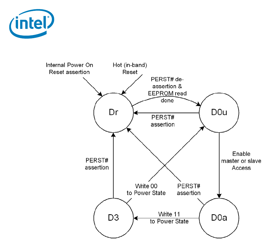
Intel® 82575EB Gigabit Ethernet Controller — Auxiliary Power
Intel® 82575EB Gigabit Ethernet Controller 324632-003
Software Developer’s Manual and EEPROM Guide Revision: 2.1
216 January 2011
Figure 23. Power States and Transitions
7.2 Auxiliary Power
If DisableD3Cold equals 0b, the 82575 uses the AUX_PWR indication that auxiliary power is available.
As a result, the 82575 advertises D3cold wakeup support. The amount of power required for the
function (this includes the entire NIC or LOM) is advertised in the Power Management Data Register,
which is loaded from the EEPROM.
If D3cold is supported, the PME_En and PME_Status bits of the Power Management Control/Status
Register (PMCSR) and their shadow bits in the Wake Up Control Register (WUC) are reset only by the
power up reset (detection of power rising).
The only effect of setting AUX_PWR to 1b is advertising D3cold wakeup support and changing the reset
function of PME_En and PME_Status. AUX_PWR is a strapping option in the 82575.
7.3 Form Factor Power Limits
The following table summarizes power limitations introduced by some of the different form factors.

Power Management Interconnects — Intel® 82575EB Gigabit Ethernet Controller
324632-003 Intel® 82575EB Gigabit Ethernet Controller
Revision: 2.1 Software Developer’s Manual and EEPROM Guide
January 2011 217
Note: This auxiliary current limit only applies when the primary 3.3V voltage source is not available. For example, the NIC is in a
low power D3 state.
The 82575 exceeds allocated auxiliary power in some configurations (for example, both ports running
at gigabit speed). as a result, the 82575 must be configured such that it meets the previously stated
requirements. To do so, the 82575 implements two EEPROM bits to disable operation in certain cases:
1. The Disable 1000 PHY CSR bit disables 1000 Mb/s operation under all conditions.
2. The Disable 1000 in non-D0a PHY CSR bit disables 1000 Mb/s operation in non-D0a states. If
Disable 1000 in non-D0a is set, and the 82575 is at gigabit speed on entry to a non-D0a state, then
it removes advertisement for 1000 and auto-negotiates.
The 82575 restarts link Auto-Negotiation each time it transitions from a state where gigabit speed is
enabled to a state where gigabit speed is disabled or vice versa. For example, if Disable 1000 Mb/s in
non-D0a is set but Disable 1000 Mb/s is clear, the 82575 restarts link Auto-Negotiation on transition
from the D0 state to D3 or Dr states.
7.4 Power Management Interconnects
This section describes the power reduction techniques employed by 82575 main interconnects.
7.4.0.1 PCIe* Link Power Management
The PCIe* link state follows the power management state of the 82575. Since the 82575 incorporates
multiple PCI functions, the device power management state is defined as the power management state
of the most awake function:
• If any function is in D0 state (either D0a or D0u), the PCIe* link assumes the 82575 is in D0 state.
Else,
• If the functions are in D3 state, the PCIe* link assumes the 82575 is in D3 state. Else,
• The 82575 is in Dr state (PE_RST_N is asserted to all functions).
The 82575 supports all PCIe* power management link states:
• L0 state is used in D0u and D0a states.
• The L0s state is used in D0a and D0u states each time link conditions apply.
• The L1 state is also used in D0a and D0u states when idle conditions apply for a longer period of
time. The L1 state is also used in the D3 state.
• The L2 state is used in the Dr state following a transition from a D3 state if PCI-PM PME is enabled.
• The L3 state is used in the Dr state when no auxiliary power is provided to the 82575.
Form Factor
LOM PCIe* NIC
Main N/A 3A @ 3.3v
Auxiliary (aux enabled) 375 mA @ 3.3V 375 mA @ 3.3v
Auxiliary (aux disabled) 20 mA @ 3.3V 20 mA @ 3.3v

Intel® 82575EB Gigabit Ethernet Controller — Power Management Interconnects
Intel® 82575EB Gigabit Ethernet Controller 324632-003
Software Developer’s Manual and EEPROM Guide Revision: 2.1
218 January 2011
82575 support for Active State Link Power Management is reported via the PCIe* Active State Link PM
Support register loaded from the EEPROM.
While in L0 state, the 82575 transitions the transmit lane(s) into L0s state once the idle conditions are
met for a period of time as shown in Figure 24.
L0s configuration fields are:
• L0s enable - The default value of the Active State Link PM Control field in the PCIe* Link Control
register is set to 00b (both L0s and L1 disabled). System software can later write a different value
into the Link Control register. The default value is loaded on any reset of the PCI configuration
registers.
• The L0S_ENTRY_LAT bit in the PCIe* Control register (GCR), determines L0s entry latency. When
set to 0b, L0s entry latency is the same as L0s Exit latency of the 82575 at the other end of the
link. When set to 1b, L0s entry latency is (L0s Exit Latency of the 82575 at the other end of the link
/4). Default value is 0b (entry latency is the same as L0s Exit latency of the 82575 at the other end
of the link).
• L0s exit latency (as published in the L0s Exit Latency field of the Link Capabilities register) is loaded
from EEPROM. Separate values are loaded when the 82575 shares the same reference PCIe* clock
with its partner across the link and when the 82575 uses a different reference clock than its partner
across the link. The 82575 reports whether it uses the slot clock configuration through the PCIe*
Slot Clock Configuration bit loaded from the Slot_Clock_Cfg EEPROM bit.
• L0s Acceptable Latency (as published in the Endpoint L0s Acceptable Latency field of the Device
Capabilities register) is loaded from EEPROM.
L1 configuration fields are:
• L1 entry latency - the 82575 enters the L1 state after it has been in the L0s state (in both
directions) for a period of time determined by the Latency_To_Enter_L1 CSR register. Initial value is
loaded from the Latency_To_Enter_L1 EEPROM field.
• L1 exit latency (as published in the L1 Exit Latency field of the Link Capabilities register) is loaded
from the L1_Act_Ext_Latency Latency_To_Enter_L1 field in the EEPROM.
• L1 Acceptable Latency (as published in the Endpoint L1 Acceptable Latency field of the Device
Capabilities register) is loaded from EEPROM.
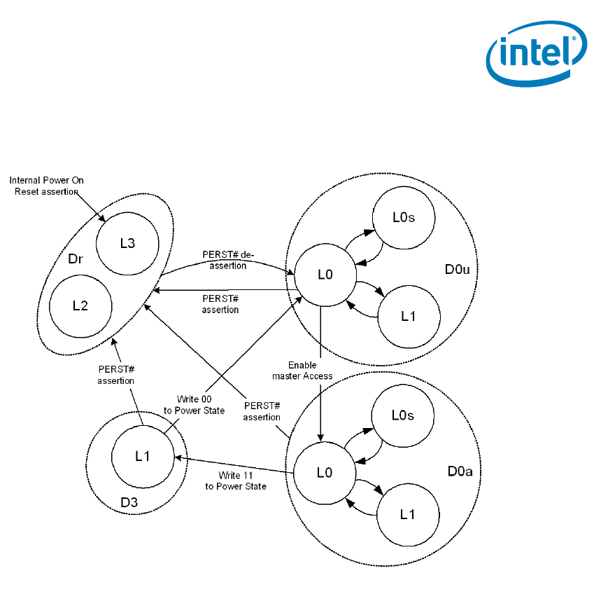
Power Management Interconnects — Intel® 82575EB Gigabit Ethernet Controller
324632-003 Intel® 82575EB Gigabit Ethernet Controller
Revision: 2.1 Software Developer’s Manual and EEPROM Guide
January 2011 219
Figure 24. Link Power Management
7.4.0.2 NC-SI Clock Control
The 82575 can be configured to provide a 50 MHz output clock to its NC-SI interface and other platform
devices. When enabled (through the NC-SI Output Clock EEPROM bit), the NC-SI clock is provided in all
power states without exception.
7.4.0.3 PHY Power Management
7.4.0.3.1 Link Speed Control
Normal PHY speed negotiation drives to establish a link at the highest possible speed. The 82575
supports an additional mode of operation where the PHY drives to establish a link at a low speed. The
link-up process allows a link to come up at the lowest possible speed in cases where power is more
important than performance. Different behavior is defined for the D0 state and the other non-D0
states.
Note: The Low Power Link Up (LPLU) feature just described should be disabled (in both D0a and
non-D0a states) when the user advertisement is anything other than 10/100/1000 Mb/s.
Intel® 82575EB Gigabit Ethernet Controller — Power Management Interconnects
Intel® 82575EB Gigabit Ethernet Controller 324632-003
Software Developer’s Manual and EEPROM Guide Revision: 2.1
220 January 2011
This avoids negotiating through the LPLU procedure a link speed that is not advertised by
the user.
The following table lists the link speed as a function of a power management state, link speed control,
and gigabit speed enabling:
The 82575 initiates auto-negotiation without a direct driver command in the following cases:
• When the state of 1000 Mb/s disable changes. For example, if 1000 Mb/s is disabled on D3 or Dr
entry (but not in D0a), the PHY auto negotiates on entry.
• When LPLU changes state with a change in PM state. For example, on transition from D0a without
LPLU to D3 with LPLU. Or, on transition from D3 w LPLU to D0 without LPLU.
• On a transition from D0a state to a non-D0a state, or from a non-D0a state to D0a state, and LPLU
is set.
7.4.0.3.2 D0a State
A power managed link speed control lowers link speed (and power) when the highest link performance
is not required. When it is enabled to this D0 Low Power Link Up mode, any link negotiation tries to
establish a low link speed, starting with an initial advertisement defined by software.
The D0 LPLU configuration bit enables D0 Low Power Link Up. Before enabling the feature, software
must advertise one of the following speed combinations: 10 Mb/s only, 10/100 Mb/s, or 10/100/1000
Mb/s.
When speed negotiation starts, the PHY tries to negotiate a speed based on the currently advertised
values. If link establishment fails, the PHY tries to negotiate with different speeds; it enables all speeds
up to the lowest speed supported by the partner. For example, the 82575 advertises
10 Mb only and the partner supports 1000 Mb only. After the first try fails, the 82575 enables 10/100/
1000 Mb/s and try again. The PHY continues to try and establish a link until it succeeds or until it is
instructed otherwise. In the second step (adjusting to partner speed), the PHY also enables parallel
detect, if needed. Automatic MDI/MDI-X resolution is done during the first auto-negotiation stage.
Power
Management
State
Low Power
Link Up
1000 Mb/s Disable Bits
PHY Speed Negotiation
Disable 1000 Disable 1000
in Non-D0a
D0a 0 0 X The PHY negotiates to the highest speed advertised (normal
operation).
1 The PHY negotiates to highest speed advertised except 1000
Mb/s.
1 0 X The PHY goes through the LPLU procedure, starting with the
advertised values.
1 The PHY goes through the LPLU procedure, starting with
advertised values but does not advertise 1000 Mb/s.
Non-D0a 0 0 0 The PHY negotiates to highest speed advertised.
0 1 The PHY negotiates to highest speed advertised except 1000
Mb/s.
1X
1 0 0 The PHY goes through the LPLU procedure, starting at 10
Mb/s.
0 1 The PHY goes through LPLU procedure, starting at 10 Mb/s
but does not advertise 1000 Mb/s.

Power Management Interconnects — Intel® 82575EB Gigabit Ethernet Controller
324632-003 Intel® 82575EB Gigabit Ethernet Controller
Revision: 2.1 Software Developer’s Manual and EEPROM Guide
January 2011 221
7.4.0.3.3 Non-D0a State
The PHY can negotiate to a low speed while in a non-D0a states (Dr, D0u, or D3). This applies only
when the link is required by SMB manageability, APM wake up, or a power management event.
Otherwise, the PHY is disabled during the non-D0 state.
The EEPROM LPLU bit enables reduction in link speed:
• On power-up entry to Dr state, the PHY advertises support for 10 Mb/s only and goes through the
link up process.
• On any entry to a non-D0a state (Dr, D0u, or D3), the PHY advertises support for 10 Mb/s only and
goes through the link up process described as follows.
• While in a non-D0 state, if auto-negotiation is required, the PHY advertises support for
10 Mb/s only and goes through the link up process.
The EEPROM LPLU bit is loaded into the LPLU configuration bit. Software can set or clear this bit at any
time. From that point on, the 82575 acts according to the latest value of the LPLU bit.
Link negotiation begins with the PHY trying to negotiate at 10 Mb/s speed only regardless of user AN
advertisement. If link establishment fails, the PHY tries to negotiate at additional speeds; it enables all
speeds up to the lowest speed supported by the partner. For example, the 82575 advertises 10 Mb only
and the partner supports 1000 Mb only. After the first try fails, the 82575 enables 10/100/1000 Mb/s
and try again. The PHY continues to try and establish a link until it succeeds or until it is instructed
otherwise. In the second step (adjusting to partner speed), the PHY also enables parallel detect, if
needed. Automatic MDI/MDI-X resolution is done during the first auto-negotiation stage.
7.4.0.3.4 Link Energy Detect
The Link Energy Detect MDIO bit is set each time energy is detected on the link. This includes the
period of time during link negotiation and when link is established. This bit should be valid immediately
after a reset of the device or the PHY.
7.4.0.3.5 PHY Power-Down State
Each of the 82575 PHYs enter a power-down state when none of its clients is enabled and therefore, no
need to maintain a link. This can happen in one of several cases as follows:
• PHY power down is enabled through the EEPROM PHY Power Down Enable bit.
• D3/Dr state - each PHY enters a low-power state if the following conditions are met:
— The LAN function associated with this PHY is in a non-D0 state.
— APM Wake on LAN* (WOL) is inactive.
— Manageability does not use this port.
— ACPI PME is disabled for this port.
• SerDes mode - each PHY is disabled when its LAN function is configured in SerDes mode.
• LAN Disable - Each PHY can be disabled if its LAN function’s LAN Disable input indicates that the
relevant function should be disabled. Since the PHY is shared between the LAN function and
manageability, it might not be desired to power down the PHY in LAN Disable. The
PHY_in_LAN_Disable EEPROM bit determines whether the PHY (and MAC) are powered down when
the LAN Disable pin is asserted. The default is not to power down.
A LAN port can also be disabled through EEPROM settings. If the LAN_DIS EEPROM bit is set, the PHY
enters power down. Note, however, that setting the EEPROM LAN_PCI_DIS bit does not bring the PHY
into power down.

Intel® 82575EB Gigabit Ethernet Controller — Power States
Intel® 82575EB Gigabit Ethernet Controller 324632-003
Software Developer’s Manual and EEPROM Guide Revision: 2.1
222 January 2011
7.4.0.3.6 SerDes/SGMII Power-Down State
Each of the 82575’s SerDes enters a power-down state when none of its clients are enabled. This case
does not require a link to be maintained. The following conditions must be met for the SerDes to enter
this power-down state:
• SerDes power down must be enabled through the EEPROM SerDes Low Power Enable bit
• D3/Dr state - each SerDes enters a low-power state if the following conditions are met:
— The LAN function associated with this SerDes is in a non-D0 state.
— APM Wake on LAN* (WOL) is inactive.
— Pass through manageability is disabled.
— ACPI PME is disabled.
• PHY mode - each SerDes is disabled when its LAN function is configured in PHY mode.
• LAN Disable - Each SerDes can be disabled if its LAN function’s LAN Disable input indicates that the
relevant function should be disabled. Since the SerDes is shared between the LAN function and
manageability, it might not be desired to power down the SerDes in LAN Disable. The
PHY_in_LAN_Disable EEPROM bit determines whether the SerDes are powered down when the LAN
Disable pin is asserted. The default is not to power down.
7.4.1 Power States
7.4.1.1 Dr State
Transition to Dr state is initiated as follows:
• On system power up. The Dr state starts with the assertion of the internal power detection circuit
(Internal_Power_On_Reset) and ends with de-asserting PE_RST_N.
• On transition from a D0a state. During operation, the system might assert PE_RST_N at any time.
In an ACPI system, a system transition to the G2/S5 state causes a transition from D0a to Dr.
• On transition from a D3 state. The system transitions the 82575 into the Dr state by asserting
PE_RST_N.
Any wake-up filter settings that were enabled before entering this reset state are maintained.
The system might maintain PE_RST_N assertion for an arbitrary time. The de-assertion (rising edge)
PE_RST_N causes a transition to the D0u state.
While in Dr state, the 82575 might enter one of several modes with different levels of functionality and
power consumption. The lower-power modes are achieved when the 82575 is not required to maintain
any functionality. The Dr Disable mode is described in “Entry to Dr State”.
Note: If the 82575 is configured to provide a 50 MHz NC-SI clock (via the NC-SI Output Clock
EEPROM bit), then the NC-SI clock must be provided in Dr state as well.
7.4.1.1.1 Dr Disable Mode
The 82575 enters a Dr Disable mode on transition to D3cold state when it does not need to maintain
any functionality. The conditions to enter either state are:
• The 82575 (all PCI functions) is in Dr state
• APM WOL is inactive for both LAN functions

Power States — Intel® 82575EB Gigabit Ethernet Controller
324632-003 Intel® 82575EB Gigabit Ethernet Controller
Revision: 2.1 Software Developer’s Manual and EEPROM Guide
January 2011 223
• Pass through manageability is disabled
• ACPI PME is disabled for all PCI functions
• The 82575 Disable Power Down En EEPROM bit is set (default hardware value is disabled).
Entry into Dr Disable is usually done after asserting PE_RST_N. It can also be possible to enter Dr
Disable mode by reading the EEPROM while already in Dr state. The usage model for this later case is at
system power up, assuming that manageability and wake up are not required. Once the 82575 enters
Dr state on power-up, the EEPROM is read. If the EEPROM contents determines that the conditions to
enter Dr Disable are met, the 82575 then enters this mode (assuming that PE_RST_N is still asserted).
Exiting from Dr Disable is by de-asserting PE_RST_N.
7.4.1.1.2 Entry to Dr State
Dr entry on platform power up starts with the assertion of the internal power detection circuit
(Internal_Power_On_Reset). The EEPROM is read and determines the 82575 configuration. If the APM
Enable bit in the EEPROM Initialization Control Word 2 is set, then APM wake up is enabled. The MAC
and PHY state is determined by the manageability state and APM wake. To reduce power consumption,
if APM Wake is enabled, the PHY auto-negotiates to a lower link speed on Dr entry. The PCIe* link is not
enabled in Dr state following system power up (since PE_RST_N is asserted).
Entry to Dr state from D0a state is by asserting PE_RST_N. An ACPI transition to the G2/S5 state is
reflected in an 82575 transition from D0a to Dr state. The transition can be orderly (programmer
selects the shut down option), in which case the software device driver can have a chance to intervene.
Or, it might be an emergency transition (power button override), in which case, the software device
driver is not notified.
To reduce power consumption if any manageability, APM wake or PCI PM PME is enabled, the PHY auto-
negotiates to a lower link speed on D0a to Dr transition.
Transition from D3 state to Dr state is done by asserting PE_RST_N. Prior to that, the system initiates a
transition of the PCIe* link from L1 state to either the L2 or L3 state (assuming all functions were
already in D3 state). The link enters L2 state if PCI-PM PME is enabled.
7.4.1.2 D0 Uninitialized State
The D0u state is a low-power state used after PE_RST_N is de-asserted following power-up (cold or
warm), on hot reset (in-band reset through PCIe* physical layer message) or on D3 exit.
When entering D0u, the 82575 disables wake ups and asserts a reset to the PHY while the EEPROM is
being read. If the APM mode bit in the EEPROM Initialization Control Word 2 is set, then APM wake up is
enabled.
7.4.1.2.1 Entry to D0u State
D0u is reached from either the Dr state (de-asserting PE_RST_N) or the D3hot state (by configuration
software writing a value of 00b to the Power State field of the PCI PM registers).
De-asserting PE_RST_N means that the entire state of the 82575 is cleared except for the sticky bits.
The state is loaded from the EEPROM. Afterwards, the PCIe* link is established. When this completes,
the configuration software can access the 82575.

Intel® 82575EB Gigabit Ethernet Controller — Power States
Intel® 82575EB Gigabit Ethernet Controller 324632-003
Software Developer’s Manual and EEPROM Guide Revision: 2.1
224 January 2011
On a transition from D3 to D0u, the 82575 PCI Configuration space is not reset. However, the 82575
requires that software perform a full re-initialization of the function including its PCI Configuration
Space.
7.4.1.3 D0 Active State
Once memory space is enabled, the 82575 enters an active state. It can transmit and receive packets if
properly configured by the driver. The PHY is enabled or re-enabled by the 82575 driver to operate/
auto-negotiate to full line speed/power if not already operating at full capability. Any APM Wakeup
previously active remains active. The driver can deactivate APM Wakeup by writing to the Wake Up
Control Register (WUC) or activate other Wake Up Filters by writing to the Wake Up Filter Control
Register (WUFC).
7.4.1.3.1 Entry to D0a State
D0a is entered from the D0u state by writing a 1b to the Memory Access Enable or the I/O Access
Enable bit of the PCI Command Register. The DMA, MAC, and PHY of the appropriate LAN function are
enabled.
7.4.1.4 D3 State
The D3 state referred to in this section is PCI PM D3hot.
The 82575 transitions to D3 when the system writes a 11b to the PowerState field of the Power
Management Control/Status register (PMCSR). Any WakeUp filter settings that were enabled before
entering this reset state are maintained. Upon transitioning to D3 state, the 82575 clears the Memory
Access Enable and I/O Access Enable bits of the PCI Command Register, which disables memory access
decode. In D3, the 82575 only responds to PCI configuration accesses and does not generate master
cycles.
Configuration and Message requests are the only TLPs accepted by a function in the D3hot state. All
other received Requests must be handled as Unsupported Requests and all received Completions can
optionally be handled as Unexpected Completions. If an error caused by a received TLP (for example,
an Unsupported Request) is detected while in D3hot, and reporting is enabled, the link must be
returned to L0 if it is not already in L0 and an error message must be sent.
A D3 state is followed by either a D0u state (in preparation for a D0a state) or by a transition to Dr
state (PCI PM D3cold state). To transition back to D0u, the system writes 00b to the Power State field of
the PMCSR. Transition to the Dr state is by asserting PE_RST_N.
7.4.1.4.1 Entry to D3 State
Transition to D3 state is through a configuration write to the Power State field of the PCI PM registers.
Prior to transition from D0 to the D3 state, the software device driver disables scheduling of further
tasks to the 82575. It masks all interrupts and does not write to the transmit descriptor tail register or
to the receive descriptor tail register and operates the master disable algorithm. If wake up capability is
needed, the software device driver should set up the appropriate wake up registers and the system
should write a 1b to the PME_En bit of the PMCSR or to the Auxiliary Power PM Enable bit of the PCIe*
Device Control Register before the transition to D3.

Power States — Intel® 82575EB Gigabit Ethernet Controller
324632-003 Intel® 82575EB Gigabit Ethernet Controller
Revision: 2.1 Software Developer’s Manual and EEPROM Guide
January 2011 225
As a response to being programmed into the D3 state, the 82575 brings its PCIe* link into the L1 link
state. As part of the transition into the L1 state, the 82575 suspends scheduling of new TLPs and waits
for the completion of all previous TLPs it has sent. The 82575 clears the Memory Access Enable and I/O
Access Enable bits of the PCI Command Register, which disables memory access decode. Any receive
packets that have not been transferred into system memory is kept in the 82575 and discarded later on
D3 exit. Any transmit packets that have not been sent can still be transmitted, assuming the Ethernet
link is valid.
To reduce power consumption, if APM wake or PCI PM PME is enabled, the PHY auto-negotiates to a
lower link speed on D3 entry.
7.4.1.4.2 Master Disable
System software can disable master accesses on the PCIe* link by either clearing the PCI Bus Master
bit or by bringing the function into a D3 state. From this point on, the 82575 must not issue master
accesses for this function. Due to the full duplex nature of PCIe* and the pipelined design in the 82575,
multiple requests from several functions might be pending when the master disable request arrives.
The protocol described in this section ensures that a function does not issue master requests to the
PCIe* link after its master enable bit is cleared or after entry to D3 state.
Two configuration bits are provided for the handshake between the 82575 function and its driver:
•GIO Master Disable bit in the Device Control Register (CTRL). When the GIO Master Disable bit is
set, the 82575 blocks new master requests, including manageability requests, by this function. The
82575 then proceeds to issue any pending requests by this function. This bit is cleared on master
reset (Internal_Power_On_Reset all the way to Software Reset) to allow master accesses.
•GIO Master Enable Status bits in the Device Status Register. These bits are cleared by the 82575
when the GIO Master Disable bit is set and no master requests are pending by the relevant
function. Otherwise, these bits are set. This indicates that no master requests is issued by this
function as long as the GIO Master Disable bit is set. The following activities must end before the
82575 clears the GIO Master Enable Status bit.
• Master requests by the transmit and receive engines
• Master requests by the manageability agents
• Reception of firmware indication that the interface to this function is Idle
• All pending completions to the 82575 are received
Note: The software device driver sets the GIO Master Disable bit when notified of a pending
master disable (or D3 entry). The 82575 then blocks new requests and proceeds to issue
any pending requests by this function. The driver then polls the GIO Master Enable Status
bit. Once the bit is cleared, it is guaranteed that no requests are pending from this function.
The driver might time-out if the GIO Master Enable Status bit is not cleared within a given
time.
The GIO Master Disable bit must be cleared to enable a master request to the PCIe* link.
This can be done either through reset or by the software device driver.
7.4.1.5 Link-Disconnect
In any of D0u, D0a, D3, or Dr, the 82575 enters a link-disconnect state if it detects a link-disconnect
condition on the Ethernet Link. Note that the link-disconnect state is invisible to software (other than
the Link Energy Detect bit state). In particular, while in D0 state, software might be able to access any
of the device registers as in a link-connect state.
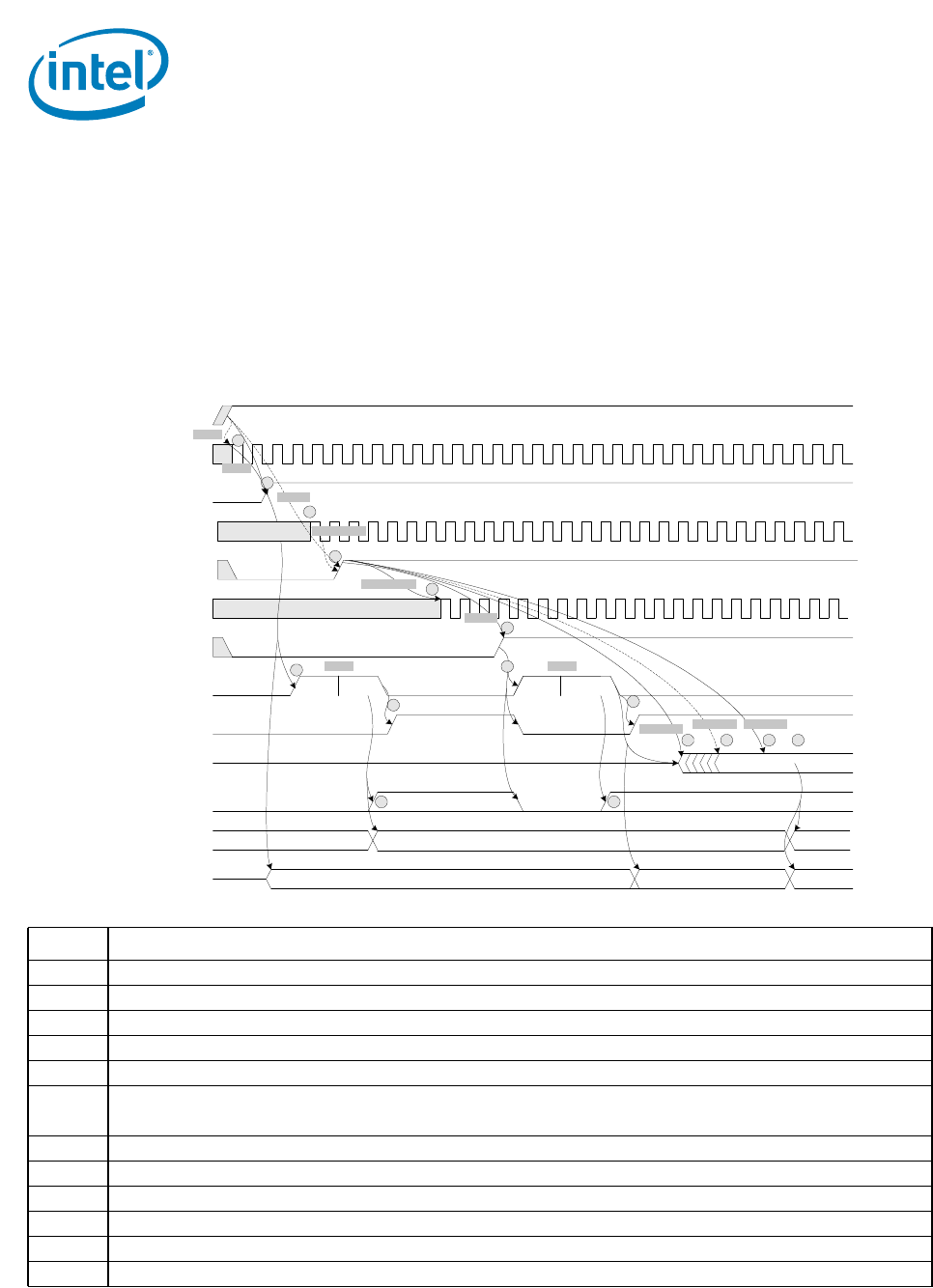
Intel® 82575EB Gigabit Ethernet Controller — Power-State Transitions Timing
Intel® 82575EB Gigabit Ethernet Controller 324632-003
Software Developer’s Manual and EEPROM Guide Revision: 2.1
226 January 2011
7.4.2 Power-State Transitions Timing
The following sections give detailed timing for the state transitions. The timing diagrams are not to
scale, and the dotted connecting lines represent the 82575 requirements, and the solid connecting
lines, 82575 guarantees. The clocks edges are shown to indicate running clocks only. They are not used
to indicate the actual number of cycles for any operation.
7.4.2.1 Power Up (Off to Dup to D0u to D0a)
Notes
1 Xosc is stable txog after the power is stable.
2 Internal_Power_On_Reset is asserted after all power supplies are good and tppg, after Xosc, is stable.
3 An EEPROM read starts on the rising edge of Internal_Power_On_Reset.
4 After reading the EEPROM, the PHY reset is de-asserted.
5 APM wake-up mode may be enabled based on what is read from the EEPROM.
6 The PCIe* reference clock is valid tPWRGDPE_RST-CLK before the assertion of PE_RST_N.
Per the PCIe* Specification.
7 PE_RST_N is asserted tPVPGL after power is stable.
8 The Internal PCIe* clock is valid and stable tppg-clkint from PE_RST_N de-assertion.
9 The PCIe* internal PE_RST_N signal is asserted tclkpr after the external PE_RST_N signal.
10 Assertion of the internal PCIe* PE_RST_N causes the EEPROM to be re-read, asserts PHY reset, and disables wake up.
11 After reading the EEPROM, PHY reset is de-asserted.
12 Link training starts after tpgtrn from PE_RST_N de-assertion.
Internal PCIe*
Clock (2.5 GHz)
Internal PwrGd (PLL)
DState D0u
Reading EEPROM
D0a
PHY Reset
PCIe* Link Up L0
Wakeup Enabled
4
5
7
Dr
10
11
12
3
5
APM/SMBus Wakeup
Power
Internal Power On
Reset
2
PCIe*
Reference Clock
PwrGd (PCIe*)
Read
3GIO
Read
rest
Read
3GIO
Read
rest
Xosc
1
6
8
txog
tee tee
9
tppg-clkint
13 14
PHY Power State Iddq Power-managed (Iddq or reduced link speed) On
APM/SMBus Wakeup
tpgtrn
15
tpgres
tpgcfg
tPWRGD-CLK
tPVPGL
tppg
tclkpr
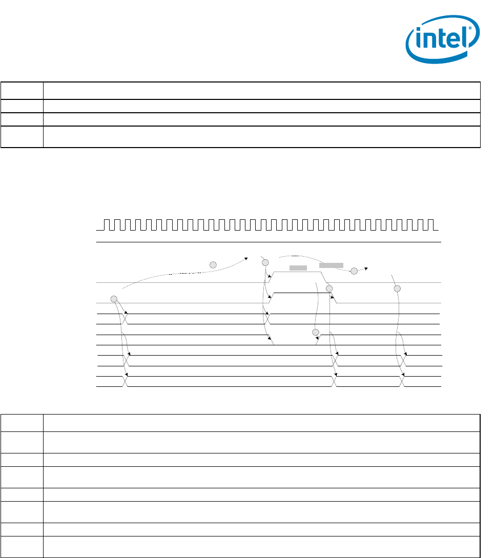
Power-State Transitions Timing — Intel® 82575EB Gigabit Ethernet Controller
324632-003 Intel® 82575EB Gigabit Ethernet Controller
Revision: 2.1 Software Developer’s Manual and EEPROM Guide
January 2011 227
7.4.2.2 Transition from D0a to D3 and Back without PE_RST_N
13 A first PCIe* configuration access might arrive after tpgcfg from PE_RST_N de-assertion.
14 A first PCIe* configuration response can be sent after tpgres from PE_RST_N de-assertion.
15 Writing a 1b to the Memory Access Enable bit in the PCI Command Register transitions the 82575 from D0u to D0
state.
Notes
1 Writing 11b to the Power State field of the Power Management Control/Status Register (PMCSR) transitions the 82575
to D3.
2 The system keeps the 82575 in D3 for an arbitrary amount of time.
3 To exit D3, the system writes 00b to the Power State field of the Power Management Control/Status Register
(PMCSR).
4 APM wake up or SMB mode can be enabled based on the EEPROM contents.
5 After reading the EEPROM, the reset to the PHY is de-asserted. The PHY operates at a reduced speed if APM wake up
or SMB is enabled. Otherwise, it is powered down.
6 The system can delay an arbitrary time before enabling memory access.
7 Writing a 1b to the Memory Access Enable bit or to the I/O Access Enable bit in the PCI Command Register transitions
the 82575 from D0u to D0 and returns the PHY to full power and full speed operation.
Notes
PCIe*
Reference Clock
PCIe* PwrGd
PHY Reset
PCIe* Link
Reading EEPROM Read EEPROM
DState D3 D0u D0
Wakeup Enabled
Memory Access Enable
L0
D3 write
APM / SMBusAny mode
D0 Write
D0a
2
L1 L0
PHY Power State full FullPower Managed Power Managed
tee
1
3
4
5
6
7
td0mem
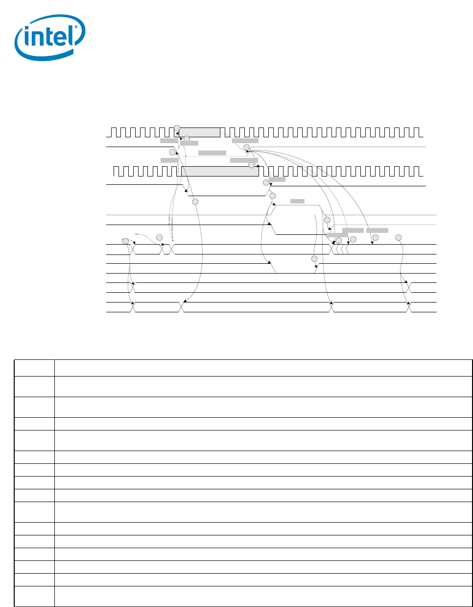
Intel® 82575EB Gigabit Ethernet Controller — Power-State Transitions Timing
Intel® 82575EB Gigabit Ethernet Controller 324632-003
Software Developer’s Manual and EEPROM Guide Revision: 2.1
228 January 2011
7.4.2.3 Transition from D0a to D3 and Back with PE_RST_N
Notes
1 Writing 11b to the Power State field of the Power Management Control/Status Register (PMCSR) transitions the 82575
to D3. The PCIe* link transitions to L1 state.
2 The system can delay an arbitrary amount of time between setting the D3 mode and transitioning the link to an L2 or
L3 state.
3 After a link transition, PE_RST_N is asserted.
4 The system must assert PE_RST_N before stopping the PCIe* reference clock. It must also wait tl2clk after link
transition to L2 or L3 before stopping the reference clock.
5 When PE_RST_N is asserted, the 82575 transitions to Dr state.
6 The system starts the PCIe* reference clock tPWRGDPE_RST-CLK before de-asserting PE_RST_N.
7 The internal PCIe* clock is valid and stable tppg-clkint from PE_RST_N de-assertion.
8 The PCIe* internal PE_RST_N signal is asserted tclkpr after the external PE_RST_N signal.
9 Assertion of the internal PCIe* PE_RST_N causes the EEPROM to be re-read, asserts a PHY reset, and disables wake
up.
10 APM wake-up mode might be enabled based on the EEPROM contents.
11 After reading the EEPROM, the PHY reset is de-asserted.
12 Link training starts after tpgtrn from PE_RST_N de-assertion.
13 A first PCIe* configuration access might arrive after tpgcfg from PE_RST_N de-assertion.
14 A first PCIe* configuration response can be sent after tpgres from PE_RST_N de-assertion.
15 Writing a 1b to the Memory Access Enable bit in the PCI Command Register transitions the 82575 from D0u to D0
state.
PCIe*
Reference Clock
PCIe* PwrGd
DState
PHY Power State
D0u
Reading EEPROM Read EEPROM
D0a
Power Managed Full
Reset to PHY
(active low)
PCIe* Link
Wakeup Enabled
Dr
11
Any Mode APM/SMBus
Full
D3 Write
D0a D3
15
L0 L1 L2/L3 L0
12
6
13 14
3
4a
4b
12
Internal PCIe*
Clock (2.5 GHz)
Internal PwrGd (PLL)
9
7
8
10
tee
tppg-clkint
tpgtrn
tpgres
tpgcfg
tclkpr
tpgdl
tl2clk
tclkpg tPWRGD-CLK
tl2pg
5
L0

Power-State Transitions Timing — Intel® 82575EB Gigabit Ethernet Controller
324632-003 Intel® 82575EB Gigabit Ethernet Controller
Revision: 2.1 Software Developer’s Manual and EEPROM Guide
January 2011 229
7.4.2.4 D0a to Dr and Back without Transition to D3
7.4.2.5 Timing Requirements
The 82575 requires the following start up and power state transitions.
Notes
1 The system must assert PE_RST_N before stopping the PCIe* reference clock. It must also wait tl2clk after link
transition to L2 or L3 before stopping the reference clock.
2 When PE_RST_N is asserted, the 82575 transitions to Dr state and the PCIe* link transitions to an electrical idle.
3 The system starts the PCIe* reference clock tPWRGDPE_RST-CLK before de-asserting PE_RST_N.
4 The internal PCIe* clock is valid and stable tppg-clkint from PE_RST_N de-assertion.
5 The PCIe* internal PE_RST_N signal is asserted tclkpr after the external PE_RST_N signal.
6 Assertion of the internal PCIe* PE_RST_N causes the EEPROM to be re-read, asserts a PHY reset, and disables wake
up.
7 APM wake-up mode can be enabled based on the EEPROM contents.
8 After reading the EEPROM, PHY reset is de-asserted.
9 Link training starts after tpgtrn from PE_RST_N de-assertion.
10 A first PCIe* configuration access might arrive after tpgcfg from PE_RST_N de-assertion.
11 A first PCIe* configuration response can be sent after tpgres from PE_RST_N de-assertion.
12 Writing a 1b to the Memory Access Enable bit in the PCI Command Register transitions the 82575 from D0u to D0
state.
PCIe*
Reference Clock
PCIe* PwrGd
DState
PHY Power State
D0u
Reading EEPROM Read EEPROM
D0a
Power Managed Full
Reset to PHY
(Active Low)
PCIe* Link
Wakeup Enabled
Dr
8
Any Mode APM/SMBus
Full
D0a
12
L0 L0
2
3
10 11
1
9
Internal PCIe*
Clock (2.5 GHz)
Internal PwrGd (PLL)
6
4
5
7
tee
tppg-clkint
tpgtrn
tpgres
tpgcfg
tclkpr
tpgdl
tclkpg tPWRGD-CLK

Intel® 82575EB Gigabit Ethernet Controller — 82575 and SerDes Power-Down State
Intel® 82575EB Gigabit Ethernet Controller 324632-003
Software Developer’s Manual and EEPROM Guide Revision: 2.1
230 January 2011
7.4.2.6 Timing Guarantees
The 82575 guarantees the following start up and power state transition related timing parameters.
7.4.3 82575 and SerDes Power-Down State
7.4.3.1 SerDes Power-Down State
The SerDes enters a power-down state when none of its clients is enabled and therefore, no need to
maintain a link. The following conditions must be met for the SerDes to enter a power-down mode:
• SerDes power-down is enabled through either the EEPROM SerDes Low Power Enable bit or the
same bit in CTRL_EXT.
• The LAN function associated with this SerDes is in a non-D0 state.
• APM WOL is inactive.
• ACPI PME is disabled for both LAN functions (in some Dr cases, ACPI power management is
irrelevant).
Parameter Description Min Max Notes
txog Xosc stable from power stable. 10 ms
tPWRGDPE_RST
-CLK
PCIe* clock valid to PCIe* power
good.
100 μs - As per PCIe* Specification.
tPVPGL Power rails stable to PCIe* PE_RST_N
in active
100 ms - As per PCIe* Specification.
Tpgcfg External PE_RST_N signal to first
configuration cycle.
100 ms As per PCIe* Specification.
td0mem 82575 programmed from D3hot to D0
state to next 82575 access.
10 ms As per PCIe* Management Specification.
tl2pg L2 link transition to PE_RST_N de-
assertion.
0 ns As per PCIe* Specification.
tl2clk L2 link transition to removal of PCIe*
reference clock.
100 ns As per PCIe* Specification.
Tclkpg PE_RST_N de-assertion to removal of
PCIe* reference clock.
0 ns As per PCIe* Specification.
Tpgdl PE_RST_N assertion time. 100 μs As per PCIe* Specification.
Parameter Description Min Max Notes
txog Xosc stable from power stable. 10 ms
tppg Internal power good delay from valid
power rail.
35 ms 35ms
tee EEPROM read duration. - 20 ms
tppg-clkint PCIe* PE_RST_N to internal PLL lock. 50 μs
tclkpr Internal PCIe* PE_RST_N from
external PCIe* PE_RST_N.
50 μs
tpgtrn PCIe* PE_RST_N to start of link
training.
20 ms As per PCIe* Specification.
Tpgres External PE_RST_N response to first
configuration cycle.
1 s As per PCIe* Specification.

Wake Up — Intel® 82575EB Gigabit Ethernet Controller
324632-003 Intel® 82575EB Gigabit Ethernet Controller
Revision: 2.1 Software Developer’s Manual and EEPROM Guide
January 2011 231
The SerDes also enters a power-down state in the following cases:
• When the 82575 is configured for PHY operation only.
• When the LAN0_DIS_N (or LAN1_DIS_N) signal for this LAN function indicates that the relevant
function should be disabled and the EEPROM SerDes Low-Power Enable bit is set.
7.4.3.2 82575 Power-Down State
The 82575 enters a global power-down state if all of the following conditions are met:
• The 82575 Power-Down Enable EEPROM bit was set (default hardware value is disabled).
• The 82575 is in Dr state.
• The link connections of both ports (PHY or SerDes) are in power down mode.
The 82575 also enters a power-down state when the DEV_OFF_N pin is active and the relevant EEPROM
bits were configured as previously stated. In addition, the manageability firmware can decide to power
down the 82575.
7.5 Wake Up
The 82575 supports two modes of wakeup management:
1. Advanced Power Management wakeup (APM).
2. ACPI/PCIe* defined wakeup.
The usual model is to activate only one of the two modes at a time but not both. If both modes are
activated at the same time, the 82575 might wakeup the system in unexpected events. For example, if
APM is enabled together with PCIe* PME, a magic packet might wakeup the system even if APMPME is
disabled, alternatively, if APM is enabled together with some PCIe* filters, packets matching these
filters might wakeup the system even if PCIe* PME is disabled.
7.5.1 Advanced Power Management Wakeup
Advanced Power Management Wake Up, or APM Wake Up, was previously known as Wake on LAN
(WOL). It is a feature that has been present in the 10/100 Mb/s NICs for several generations. Its basic
function is to receive a broadcast or unicast packet with an explicit data pattern and respond by
asserting a wake-up signal to notify the system about a wake-up event. In the earlier generations, this
was accomplished by using a special signal that ran across a cable to a defined connector on the
motherboard. The adapter asserted the signal for approximately 50 ms to signal a wake up. If the
82575 is configured appropriately, it uses an in-band PM_PME message to achieve this.
At power up, the 82575 reads the APM Enable bits from the EEPROM Initialization Control Word 2 into
the APM Enable (APME) bits of the Wakeup Control Register (WUC). These bits enable APM Wake Up.
When APM Wake Up is enabled, the 82575 checks all incoming packets for Magic Packets*. When the
82575 receives a matching Magic Packet, it acts accordingly. If the Assert PME on APM Wake Up
(APMPME) bit is set in the WUC register, the 82575:
• Sets the PME_Status bit in the PMCSR and issues a PM_PME message. In some cases, this might
first require assertion of the WAKE# signal to resume power and clock to the PCIe* interface.
• Stores the first 128 bytes of the packet in the Wake Up Packet Memory (WUPM).

Intel® 82575EB Gigabit Ethernet Controller — PCIe Power Management Wakeup
Intel® 82575EB Gigabit Ethernet Controller 324632-003
Software Developer’s Manual and EEPROM Guide Revision: 2.1
232 January 2011
• Sets the Magic Packet Received bit in the Wake Up Status Register (WUS).
• Sets the packet length in the Wake Up Packet Length Register (WUPL).
The 82575 maintains the first magic packet received in the Wake Up Packet Memory (WUPM) until the
software device driver writes a 1b to the Magic Packet Received MAG bit in the Wake Up Status Register
(WUS).
APM Wake Up is supported in all power states and only disabled if a subsequent EEPROM read results in
a cleared APM Wake Up bit or software explicitly writes a 0b to the APM Wake Up (APM) bit of the WUC
register.
7.5.2 PCIe Power Management Wakeup
• The 82575 supports PCIe* Power Management based wake ups. It can generate system wake-up
events from three sources:
• Reception of a Magic Packet.
• Reception of a network wake-up packet.
• Detection of a link change of state.
Activating PCIe* Power Management Wake Up requires the following steps:
• The driver programs the WUFC register indicating the wake-up packets. It also supplies the
necessary data to the IPv4 and IPv6 Address Table (IP4AT and IP6AT) and the Flexible Filter Mask
Table (FFMT), and the Flexible Filter Value Table (FFVT). It can also set the Link Status Change
(LNKC) bit in the Wake Up Filter Control Register (WUFC) to cause wake up when the link changes
state.
• At configuration time, the operating system writes a 1b to the PME_EN bit of the PMCSR.
After enabling wake up, the operating system typically writes 11b to the lower two bits of the PMCSR
placing the 82575 into low-power mode.
After wake up is enabled, the 82575 monitors the incoming packets. First, it filters the packets
according to its standard address filtering method and then filtering them with all of the enabled wake-
up filters. If a packet passes both the standard address filtering and at least one of the enabled wake-
up filters, the 82575:
• Sets the PME_Status bit in the PMCSR.
• If the PME_EN bit in the PMCSR is set, assert PE_WAKE_N or send a PM-PME message as defined in
the PCIe* specification.
• Stores the first 128 bytes of the packet in the Wake Up Packet Memory.
• Sets one or more of the received bits in the Wake Up Status Register (WUS). (The 82575 sets more
than one bit if a packet matches more than one filter.)
• Sets the packet length in the Wake Up Packet Length Register (WUPL).
If enabled, a link state change wake up causes similar results, setting PME_Status, asserting
PE_WAKE_N and setting the Link Status Changed (LNKC) bit in the Wake Up Status Register (WUS)
when the link goes up or down.
The 82575 supports the following change described in the PCIe* Base Specification, Rev. 1.1RD
(section 5.3.3.4): On receiving a PME_Turn_Off Message, the 82575 must block the transmission of
PM_PME Messages and transmit a PME_TO_Ack Message upstream. The 82575 is permitted to send a
PM_PME Message after the Link is returned to an L0 state through LDn.

Wake-Up Packets — Intel® 82575EB Gigabit Ethernet Controller
324632-003 Intel® 82575EB Gigabit Ethernet Controller
Revision: 2.1 Software Developer’s Manual and EEPROM Guide
January 2011 233
PE_WAKE_N remains asserted until the operating system either writes a 1b to the PME_Status bit of the
PMCSR or writes a 0b to the PME_EN bit.
After receiving a wake-up packet, the 82575 ignores any subsequent wake-up packets until the
software device driver clears all of the received bits in the Wake Up Status Register (WUS). It also
ignores link change events until the software device driver clears the Link Status Change (LNKC) bit in
the WUS.
Note: Wake on link change is not supported when in SerDes mode.
7.5.3 Wake-Up Packets
The 82575 supports various wakeup packets using two types of filters:
• Pre-defined filters
• Flexible filters
Each of these filters are enabled if the corresponding bit in the Wake Up Filter Control register (WUFC)
is set to 1b.
7.5.3.1 Pre-Defined Filters
The following packets are supported by the 82575 pre-defined filters:
• Directed Packet (including exact, multicast, and broadcast).
• Magic Packet.
• ARP/IPv4 Request Packet.
• Directed IPv4 Packet.
• Directed IPv6 Packet.
Each of these filters are enabled if the corresponding bit in the Wake Up Filter Control Register (WUFC)
is set to 1b.
The explanation of each filter includes a table detailing which bytes at which offsets are compared to
determine if the packet passes the filter. Both VLAN frames and LLC/Snap frames can increase the
given offsets if they are present.
7.5.3.1.1 Directed Exact Packet
The 82575 generates a wake-up event upon reception of any packet whose destination address
matches one of the 16 valid programmed Receive Addresses if the Directed Exact Wake Up Enable bit is
set in the Wake Up Filter Control Register (WUFC.EX).
7.5.3.1.2 Directed Multicast Packet
Offset Number of
Bytes Field Value Action Comment
0 6 Destination Address Compare Match any pre-programmed address.

Intel® 82575EB Gigabit Ethernet Controller — Wake-Up Packets
Intel® 82575EB Gigabit Ethernet Controller 324632-003
Software Developer’s Manual and EEPROM Guide Revision: 2.1
234 January 2011
For multicast packets, the upper bits of the destination address in the incoming packet index a bit
vector. This is the Multicast Table Array that indicates whether to accept the packet. If the Directed
Multicast Wake Up Enable bit is set in the Wake Up Filter Control Register (WUFC.MC) and the indexed
bit in the vector is 1b, then the 82575 generates a wake-up event. The exact bits used in the
comparison are programmed by software in the Multicast Offset field of the Receive Control Register
(RCTL.MO).
7.5.3.1.3 Broadcast
If the Broadcast Wake Up Enable bit in the Wake Up Filter Control Register (WUFC.BC) is set, the 82575
generates a wake-up event when it receives a broadcast packet.
7.5.3.1.4 Magic Packet*
The definition for a Magic Packet* can be located at:
http://www.amd.com/us-en/assets/content_type/white_papers_and_tech_docs/20213.pdf.
The 82575 expects the destination address to either:
• Be the broadcast address (FF.FF.FF.FF.FF.FF).
• Match the value in the Receive Address Register 0 (RAH0, RAL0). This is initially loaded from the
EEPROM but might be changed by the software device driver.
• Match any other address filtering enabled by the software device driver.
The 82575 looks for the contents of Receive Address Register 0 (RAH0, RAL0) as the embedded IEEE
address. It will consider any non-FFh byte after a series of at least 6 FFs to be the start of the IEEE
address for comparison purposes. For example, it catches the case of 7 FFs followed by the IEEE
address. As soon as one of the first 96 bytes after a string of FFs does not match, it continues to search
for anther set of at least 6 FFs followed by the 16 copies of the IEEE address later in the packet. It
should be noted that this definition precludes the first byte of the destination address from equaling FF.
A Magic Packet destination address must match the address filtering enabled in the configuration
registers with the exception that broadcast packets will be considered to match even if the Broadcast
Accept bit of the Receive Control Register (RCTL.BAM) is 0b. If APM Wake Up is enabled in the EEPROM,
the 82575 starts with the Receive Address Register 0 (RAH0, RAL0) loaded from the EEPROM. This
allows the 82575 to accept packets with the matching IEEE address before the driver comes up.
Offset Number of
Bytes Field Value Action Comment
0 6 Destination Address Compare See above paragraph.
Offset Number of
Bytes Field Value Action Comment
0 6 Destination Address ff*6 Compare
Offset Number of
Bytes Field Value Action Comment
Wake-Up Packets — Intel® 82575EB Gigabit Ethernet Controller
324632-003 Intel® 82575EB Gigabit Ethernet Controller
Revision: 2.1 Software Developer’s Manual and EEPROM Guide
January 2011 235
Note: Accepting broadcast magic packets for wake up purposes when Broadcast Accept bit of the
Receive Control Register (RCTL.BAM) is 0b differs from older generation Intel Gigabit
Ethernet components. Previously, these devices initialized RCTL.BAM to 1b if APM was
enabled in the EEPROM but then required that bit to equal 1b to accept broadcast Magic
Packets, unless broadcast packets passed another perfect or multicast filter.
7.5.3.1.5 ARP/IPv4 Request Packet
The 82575 supports the reception of ARP request packets for wake up if the ARP bit is set in the Wake
Up Filter Control Register (WUFC). Four IPv4 addresses are supported and are programmed in the IPv4
Address Table (IP4AT). A successfully matched packet must contain a broadcast MAC address, a
Protocol Type of 0806h, an ARP OPCODE of 01h, and one of the four programmed IPv4 addresses. The
82575 also handles ARP request packets with VLAN tagging on both Ethernet II and Ethernet SNAP
types.
7.5.3.1.6 Directed IPv4 Packet
The 82575 supports the reception of Directed IPv4 packets for wake up if the IPv4 bit is set in the Wake
Up Filter Control Register (WUFC). Four IPv4 addresses are supported and are programmed in the IPv4
Address Table (IP4AT). A successfully matched packet must contain the station MAC address, a Protocol
Type of 0800h, and one of the four programmed IPv4 addresses. The 82575 also handles Directed IPv4
packets with VLAN tagging on both Ethernet II and Ethernet SNAP types.
0 6 Destination Address Compare MAC header processed by main
address filter.
6 6 Source Address Skip
12 8 Possible LLC/SNAP Header Skip
12 4 Possible VLAN Tag Skip
12 4 Type Skip
any 6 Synchronizing Stream FF*6+ Compare
any+6 96 16 copies of Node Address A*16 Compare Compared to Receive Address Register
0 (RAH0, RAL0).
Offset Number of
Bytes Field Value Action Comment
0 6 Destination Address Compare MAC header processed by main
address filter.
6 6 Source Address Skip
12 8 Possible LLC/SNAP Header Skip
12 4 Possible VLAN Tag Skip
12 2 Type 0806h Compare ARP
14 2 Hardware Type 0001h Compare
16 2 Protocol Type 0800h Compare
18 1 Hardware Size 06h Compare
19 1 Protocol Address Length 04h Compare
20 2 Operation 0001h Compare
22 6 Sender Hardware Address - Ignore
28 4 Sender IP Address - Ignore
32 6 Target Hardware Address - Ignore
38 4 Target IP Address IP4AT Compare May match any of 4 values in IP4AT.

Intel® 82575EB Gigabit Ethernet Controller — Wake-Up Packets
Intel® 82575EB Gigabit Ethernet Controller 324632-003
Software Developer’s Manual and EEPROM Guide Revision: 2.1
236 January 2011
7.5.3.1.7 Directed IPv6 Packet
The 82575 supports reception of Directed IPv6 packets for wake up if the IPv6 bit is set in the Wake Up
Filter Control Register (WUFC). One IPv6 address is supported and it is programmed in the IPv6
Address Table (IP6AT). A successfully matched packet must contain the station MAC address, a Protocol
Type of 86DDh, and the programmed IPv6 address. In addition, the IPAV.V60 bit should be set. The
82575 also handles Directed IPv6 packets with VLAN tagging on both Ethernet II and Ethernet SNAP
types.
7.5.3.2 Flexible Filter
The 82575 supports a total of four flexible filters. Each filter can be configured to recognize any
arbitrary pattern within the first 128 bytes of the packet. The flexible filter is configured by software
programming mask values into the Flexible Filter Mask Table (FFMT), required values into the Flexible
Offset Number of
Bytes Field Value Action Comment
0 6 Destination Address Compare MAC Header processed by main
address filter.
6 6 Source Address Skip
12 8 Possible LLC/SNAP Header Skip
12 4 Possible VLAN Tag Skip
12 2 Type 0800h Compare IP
14 1 Version/ HDR length 4Xh Compare Check IPv4.
15 1 Type of Service - Ignore
16 2 Packet Length - Ignore
18 2 Identification - Ignore
20 2 Fragment Information - Ignore
22 1 Time to Live - Ignore
23 1 Protocol - Ignore
24 2 Header Checksum - Ignore
26 4 Source IP Address - Ignore
30 4 Destination IP Address IP4AT Compare May match any of 4 values in IP4AT.
Offset Number of
Bytes Field Value Action Comment
0 6 Destination Address Compare MAC Header processed by main
address filter.
6 6 Source Address Skip
12 8 Possible LLC/SNAP Header Skip
12 4 Possible VLAN Tag Skip
12 2 Type 0800h Compare IP
14 1 Version / Priority 6Xh Compare Check IPv6.
15 3 Flow Label - Ignore
18 2 Payload Length - Ignore
20 1 Next Header - Ignore
21 1 Hop Limit - Ignore
22 16 Source IP Address - Ignore
38 16 Destination IP Address IP6AT Compare Match value in IP6AT.

Wake-Up Packets — Intel® 82575EB Gigabit Ethernet Controller
324632-003 Intel® 82575EB Gigabit Ethernet Controller
Revision: 2.1 Software Developer’s Manual and EEPROM Guide
January 2011 237
Filter Value Table (FFVT). These contain separate values for each filter. The software must also enable
the filter in the Wake Up Filter Control Register (WUFC) and enable the overall wake up functionality
must be enabled by setting PME_EN in the PMCSR or the WUC register.
When flexible filtering is enabled, the flexible filters scan incoming packets for a match. If the filter
encounters any byte in the packet where the mask bit is one and the byte does not match the byte
programmed in the Flexible Filter Value Table (FFVT), then the filter will fail that packet. If the filter
reaches the required length without failing the packet, it passes the packet and generates a wake-up
event. It will ignore any mask bits set to one beyond the required length.
Note: The minimum length of a flex filter is two bytes.
The following packets listed in subsequent sections are for reference purposes only. The flexible filter
can be used to filter these packets.
7.5.3.2.1 IPX Diagnostic Responder Request Packet
An IPX Diagnostic Responder Request Packet must contain a valid MAC address, a Protocol Type of
8137h, and an IPX Diagnostic Socket of 0456h. It might include LLC/SNAP headers and VLAN tags.
Since filtering this packet relies on the flexible filters, which use offsets directly specified by the
operating system, the operating system must account for the extra offset due to the LLC/SNAP headers
and VLAN tags.
7.5.3.2.2 Directed IPX Packet
A valid Directed IPX Packet contains the station MAC address, a Protocol Type of 8137h, and an IPX
Node Address equal to the station MAC address. It may include LLC/SNAP headers and VLAN tags.
Since filtering this packet relies on the flexible filters, which use offsets directly specified by the
operating system, the operating system must account for the extra offset due to the LLC/SNAP headers
and VLAN tags.
Offset Number of
Bytes Field Value Action Comment
0 6 Destination Address Compare
6 6 Source Address Skip
12 8 Possible LLC/SNAP Header Skip
12 4 Possible VLAN Tag Skip
12 2 Type 8137h Compare IPX
14 16 Some IPX Data - Ignore
30 2 IPX Diagnostic Socket 0456h Compare
Offset Number of
Bytes Field Value Action Comment
0 6 Destination Address Compare MAC Header processed by main
address filter.
6 6 Source Address Skip
12 8 Possible LLC/SNAP Header Skip
12 4 Possible VLAN Tag Skip
12 2 Type 8137h Compare IPX.
14 10 Some IPX Data - Ignore
24 6 IPX Node Address Receive
Address 0
Compare Must match Receive Address 0.

Intel® 82575EB Gigabit Ethernet Controller — Wake-Up Packets
Intel® 82575EB Gigabit Ethernet Controller 324632-003
Software Developer’s Manual and EEPROM Guide Revision: 2.1
238 January 2011
7.5.3.2.3 IPv6 Neighbor Discovery Filter
In Ipv6, a Neighbor Discovery packet is used for address resolution. A flexible filter can be used to
check for a Neighborhood Discovery Packet.
7.5.3.3 Wake Up Packet Storage
The 82575 saves the first 128 bytes of the wake-up packet in its internal buffer, which can be read
through the Wake Up Packet Memory (WUPM) after the system has been woken up.
§ §

DCA — Intel® 82575EB Gigabit Ethernet Controller
324632-003 Intel® 82575EB Gigabit Ethernet Controller
Revision: 2.1 Software Developer’s Manual and EEPROM Guide
January 2011 239
8.0 DCA
This section describes the Direct Cache Access (DCA) functionality for the 82575.
Direct Cache Access (DCA) is a method to improve network I/O performance by placing some posted
inbound writes directly within processor cache. DCA can significantly reduce processor cache miss
rates.
DCA provides a mechanism where the posted write data from an I/O device, such as an Ethernet NIC,
can be placed into the processor cache with a hardware pre-fetch. This mechanism is initialized upon a
power good reset. A software device driver for the I/O device configures it for DCA and sets up the
appropriate processor ID and bus ID for the device to send data. The device then encapsulates that
information in PCIe* TLP headers (in the TAG field) to trigger a hardware pre-fetch by the MCH to the
processor cache.
DCA implementation is controlled by separate registers (RXCTL and TXCTL) for each receive and
transmit queues. In addition, a DCA-enable bit can be found in the GCR register and a DCA_ID register
can be found for each port in order to make visible the function, device, and bus numbers to the
software device driver.
The RXCTL and TXCTL registers can be written by software and can be changed at any time. When
software changes the register contents, hardware applies changes only after all the previous packets in
progress for DCA has completed.
In order to implement DCA, the 82575 has to be aware of the data movement engine version being
used. The software device driver initializes the 82575 to make it aware of the data movement engine
version. DCA_BUS_SELECT CTRL is used in order to properly define the system configuration.
There are two modes for DCA implementation:
1. Data Movement Engine 1: The DCA target ID is derived from processor ID
2. Data Movement Engine 2: The DCA target ID is derived from APIC ID.
The software device driver selects one of these modes through the DCA Mode register.
8.1 Implementation Details
8.1.1 PCIe* Message Format for DCA (MWr Mode)
Figure 25 shows the format of the PCIe* message for DCA.
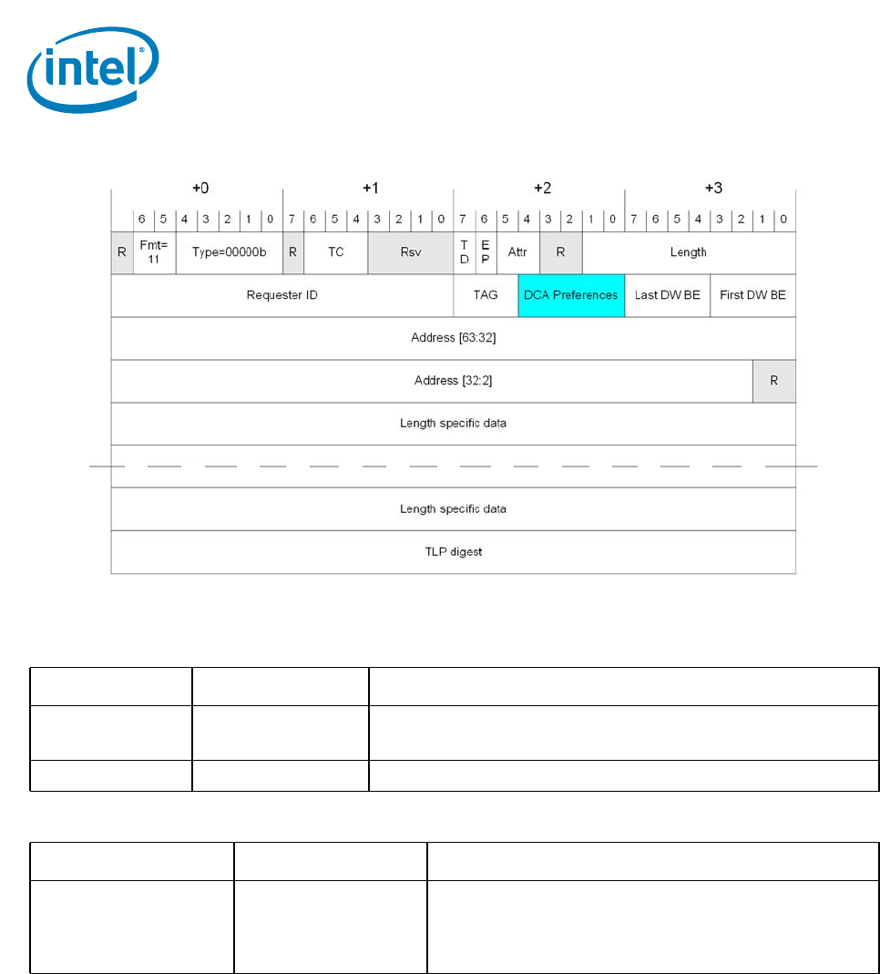
Intel® 82575EB Gigabit Ethernet Controller — PCIe* Message Format for DCA (MWr Mode)
Intel® 82575EB Gigabit Ethernet Controller 324632-003
Software Developer’s Manual and EEPROM Guide Revision: 2.1
240 January 2011
Figure 25. PCIe* Message Format for DCA
The DCA preferences field has the following formats data movement engine 1 systems:
For data movement engine 2 systems:
Note: All functions within the 82575 have to adhere to the tag encoding rules for DCA writes.
Even if a given function is not capable of DCA, but other functions are capable of DCA,
memory writes from the non-DCA function must set the tag field to 00000b.
§ §
Bits Name Description
0 DCA Indication 0b = DCA disabled.
1b = DCA enabled.
1 DCA Target ID The DCA Target ID specifies the target cache for the data.
Bits Name Description
7:0 DCA Target ID 0000,0000b: DCA is disabled
Other: Target Core Id derived from APIC ID
Note: The 82575 supports programming of only five bits of the
eight possible. In the 82575 A0, the disable tag is 11111b.
Ethernet Interface — Intel® 82575EB Gigabit Ethernet Controller
324632-003 Intel® 82575EB Gigabit Ethernet Controller
Revision: 2.1 Software Developer’s Manual and EEPROM Guide
January 2011 241
9.0 Ethernet Interface
The 82575 provides a complete CSMA/CD function supporting IEEE 802.3 (10 Mb/s), 802.3u (100 Mb/
s), 802.3z and 802.3ab (1000 Mb/s) implementations. It performs all of the functions required for
transmission, reception and collision handling called out in the standards.
• Each 82575 MAC can be configured to be used a different media interface. While the most likely
application is expected to be based on use of the internal copper PHY, the 82575 supports the
following configurations:
• Internal Copper PHY.
• External SerDes device such as an optical SerDes (SFP or onboard) or backplane connections.
• External SGMII device. This mode is used for SFP connections or external SGMII PHYs.
Selection between the various configurations is programmable via each MAC's Extended Device Control
Register (CTRL_EXT.LINK_MODE bits) and defaulted via EEPROM settings. lists the encoding on the
LINK_MODE field for each of the modes.
Table 78. Link Mode Encoding
The GMII/MII mode used to communicate between the MAC and the internal PHY and SGMII mode
supports 10/100/1000 Mb/s operation, with both half- and full-duplex operation at 10/100 Mb/s, and
full-duplex operation at 1000 Mb/s.
The SerDes function can be used to implement a Fiber/optics-based solution or backplane connection
without requiring an external transceiver/SerDes.
Note: There are two SerDes modes supported by the 82575, a legacy mode
(EXT_CTRL.LINK_MODE = 01b) and a recommended one (EXT_CTRL.LINK_MODE = 11b).
The following description refers to both modes. Both modes implement the same protocol.
However the control and status registers used in the two modes are different.
The SGMII interface can be used to connect to SFP modules; however, the following limitations apply:
• No Tx clock
• AC coupling only
Link Mode 82575 Mode
00b Internal PHY
01b Reserved
10b SGMII
11b New SerDes

Intel® 82575EB Gigabit Ethernet Controller — Internal MAC/PHY 10/100/1000Base-T Interface
Intel® 82575EB Gigabit Ethernet Controller 324632-003
Software Developer’s Manual and EEPROM Guide Revision: 2.1
242 January 2011
The internal copper PHY features 10/100/1000BASE-T signaling and is capable of performing intelligent
power-management based on both the system power-state and LAN energy-detection (detection of
unplugged cables). Power management includes ability to shut-down to extremely low (powered-down)
state when not needed as well as ability to auto-negotiate to lower-speed 10/100 Mb/s operation when
the system is in low power-states.
9.1 Internal MAC/PHY 10/100/1000Base-T
Interface
The 82575 MAC and PHY communicate through an internal 10/100/1000Base-T interface that can be
configured for either 1000 Mb/s operation (GMII) or 10/100 Mb/s (MII) mode of operation. For proper
network operation, both MAC and PHY must be properly configured (either explicitly via software or via
hardware auto-negotiation) to identical speed and duplex settings. All MAC configuration is performed
using device control registers mapped into system memory or I/O space; an internal MDIO/MDC
interface accessible via software is used to configure the PHY operation.
The internal 1000Base-T mode of operation is similar to 10/100Base-T mode of operation. 1000Base-T
mode uses the same MDIO/MDC management interface and registers for PHY configuration as 10/
100Base-T mode. These common elements of operation enable the MAC and PHY to cooperatively
determine link partner's operational capability and configure the hardware based on those capabilities.
• RX_DATA (receive data): Data received by the PHY is transferred to the MAC in 8-bit quantities at
125 MHz in GMII mode.
• RX_ER (receive error): Receive errors are detected by the PHY and signaled to the MAC. Receive
errors may include link coding errors, or any other error detected by the PHY. If receive errors
signaled during packet reception, the MAC can be configured to either receive or drop these
packets.
• RX_DV (receive data valid): This signal is asserted from the PHY to the MAC to transfer valid frame
data to the MAC. It is asserted from the first through the final bytes of a frame, de-asserted after
the final byte. The PHY asserts carriers sense with this data-valid signal de-asserted to indicate to
the MAC reception of broken packet headers (fragments).
9.1.1 MDIO/MDC
The 82575 implements an internal IEEE 802.3 MII Management Interface (also known as the
Management Data Input/Output or MDIO Interface) between the MAC and PHY. This interface provides
the MAC and software the ability to monitor and control the state of the PHY. The internal MDIO
interface defines a physical connection, a special protocol that runs across the connection, and an
internal set of addressable registers. The internal interface consists of a data line (MDIO) and clock line
(MDC), which are accessible by software via the MAC register space.
• MDC (management data clock) — This signal is used by the PHY as a clock timing reference for
information transfer on the MDIO signal. The MDC is not required to be a continuous signal and can
be frozen when no management data is transferred. The MDC signal has a maximum operating
frequency of 2.5 MHz.
• MDIO (management data I/O) — This internal signaling between the MAC and PHY logically
represents a bi-directional data signal used to transfer control information and status to and from
the PHY (to read and write the PHY management registers). Asserting and interpreting value(s) on
this interface requires knowledge of the special MDIO protocol to avoid possible internal signal
contention or miscommunication to/from the PHY.

Duplex Operation for Copper PHY Operation — Intel® 82575EB Gigabit Ethernet Controller
324632-003 Intel® 82575EB Gigabit Ethernet Controller
Revision: 2.1 Software Developer’s Manual and EEPROM Guide
January 2011 243
Software can use MDIO accesses to read or write registers in either 1000Base-T or 10/100Base-T mode
by accessing the 82575’s MDIC register.
When working in SGMII/SerDes mode, the external PHY (if applicable) can be accessed either through
MDC/MDIO as previously described or via an I2C bus using the I2CCMD register. The I2C bus or the
MDC/MDIO bus are connected via the same pins, and are mutually exclusive. In order to be able to
control an external device, either by SFP or MDC/MDIO, the I2C SFP Enable bit in Initialization Control 3
EEPROM word should be set.
As the MDC/MDIO command can be targeted either to the internal PHY or to an external bus, the
MDIC.Destination bit is used to define the target of the transaction.
Note: Each port has its own MDC/MDIO or I2C bus and there is no sharing between the ports of
the control port. In order to control both port PHYs via the same control bus, accesses to
both PHYs should be done via the same port with different device addresses.
9.2 Duplex Operation for Copper PHY
Operation
The 82575 supports half-duplex and full-duplex 10/100 Mb/s MII mode either through internal copper
PHY or SGMII interface. However, only full-duplex mode is supported when SerDes mode is used or in
any 1000 Mb/s connection.
Configuration of the duplex operation of the 82575 can be forced or determined via the Auto-
Negotiation process. See Section 9.3 for details on link configuration setup and resolution.
9.2.1 Full Duplex
All aspects of the IEEE 802.3, 802.3u, 802.3z, and 802.3ab specifications are supported in full duplex
operation. Full duplex operation is enabled by several mechanisms depending on the speed
configuration of the 82575 and the specific capabilities of the PHY used in the application. During full
duplex operation, the 82575 can transmit and receive packets simultaneously across the link interface.
In full-duplex 10/100/1000Base-T mode, transmission and reception are delineated independently by
the 10/100/1000Base-T control signals. Transmission starts upon the assertion of TX_EN, which
indicates there is valid data on the TX_DATA bus driven from the MAC to the PHY. Reception is signaled
by the PHY by the assertion of the RX_DV signal which indicates valid receive data on the RX_DATA
lines to the MAC.
In SerDes mode, the transmission and reception of packets is indicated by symbols imbedded in the
data stream. These symbols delineate the packet encapsulation and the protocol does not rely on other
control signals.

Intel® 82575EB Gigabit Ethernet Controller — Half Duplex
Intel® 82575EB Gigabit Ethernet Controller 324632-003
Software Developer’s Manual and EEPROM Guide Revision: 2.1
244 January 2011
9.2.2 Half Duplex
In half duplex mode, the 82575 attempts to avoid contention with other traffic on the wire, by
monitoring the carrier sense signal provided by the PHY, and deferring to passing traffic. When the
Internal Carrier Sense signal is deasserted or after sufficient InterPacket Gap (IPG) has elapsed after a
transmission, frame transmission can begin. The MAC signals the PHY with TX_EN at the start of
transmission.
In the case of a collision, the PHY/SGMII detects the collision and asserts the COL signal to the MAC.
Transmission of the frame stops within four link clock times, and the 82575 sends a JAM sequence onto
the link. After the end of a collided transmission, the 82575 backs off and attempt to retransmit per the
standard CSMA/CD method. Note that the re-transmissions are done from the data stored internally in
the 82575 MAC transmit packet buffer (no re-access to the data in host memory is performed).
The MAC behavior is different if a regular collision or a late collision is detected. If a regular collision is
detected, the MAC always tries to retransmit until the number of excessive collision is reached. In case
of late collision, the MAC retransmission is configurable. In addition, statistics are gathered on late
collisions.
In the case of a successful transmission, the 82575 is ready to transmit any other frame(s) queued in
the MAC’s transmit FIFO after the minimum Inter Frame Spacing (IFS) of the link has elapsed.
During transmit, the PHY is expected to signal a carrier-sense (assert the CRS signal) back to the MAC
before one slot time has elapsed. The transmission completes successfully even if the PHY fails to
indicate CRS within the slot time window; if this situation occurs, the PHY can either be configured
incorrectly or be in a link down situation. Such an event is counted in the Transmit without CRS statistic
register (see Section 14.8.12).
9.2.3 Gigabit Physical Coding Sub-Layer (PCS) for
SerDes
The 82575 integrates the 802.3z PCS function on-chip. The on-chip PCS circuitry is used when the link
interface is configured for Serdes or SGMII operation and is bypassed for internal PHY mode.
The packet encapsulation is based on the Fibre Channel physical layer (FC0/FC1) and uses the same
coding scheme to maintain transition density and DC balance. The physical layer device is the SerDes
and is used for 1000BASE-SX, -LX, or -CX configurations.
9.2.3.1 8B10B Encoding/Decoding
The Gigabit PCS circuitry uses the same transmission coding scheme used in the Fibre Channel physical
layer specification. The 8B10B coding scheme was chosen by the IEEE standards committee in order to
provide a balanced, continuous stream with sufficient transition density to allow for clock recovery at
the receiving station. There is a 25 percent overhead for this transmission code which accounts for the
data signaling rate of 1250 Mb/s with 1000 Mb/s of actual data.
SGMII Encoding in 10/100 Mb/s — Intel® 82575EB Gigabit Ethernet Controller
324632-003 Intel® 82575EB Gigabit Ethernet Controller
Revision: 2.1 Software Developer’s Manual and EEPROM Guide
January 2011 245
9.2.3.2 Code Groups and Ordered Sets
Code group and ordered set definitions are defined in clause 36 of the IEEE 802.3z standard. These
represent special symbols used in the encapsulation of Gigabit Ethernet packets. Table 79 lists a brief
description of defined ordered sets for informational purposes only.
Table 79. Code Group and Ordered Set Usage
9.2.4 SGMII Encoding in 10/100 Mb/s
When working in SGMII mode at 10 or 100 Mb/s, the code group of each byte is duplicated 100 or 10
times respectively, in order to match the link rate and the SerDes interface rate. The 82575 samples
one copy from each received set before sending it to the MAC.
Note: If an RXERR is asserted (1b), one of the replications might be ignored by the 82575. In this
case the packet might be accepted or dropped due to subsequent CRC errors. This behavior
might be observed depending on the placement of the external PHY.
Code Ordered_Set # of Code
Groups Usage
/C/ Configuration 4 General reference to configuration ordered sets, either
/C1/ or /C2/, which is used during Auto Negotiation to advertise &
negotiate link operation information between link partners. Last two code
groups contain config base and next page registers.
/C1/ Configuration 1 4 See /C/. Differs from /C2/ in second code group for maintaining proper
signaling disparity.
/C2/ Configuration 2 4 See /C/. Differs from /C1/ in second code group for maintaining proper
signaling disparity.
/I/ IDLE 2 General reference to IDLE ordered sets. IDLE characters are continually
transmitted by the end stations and are replaced by encapsulated packet
data. The transitions in the IDLE stream allow the SerDes to maintain clock
and symbol synchronization between to link partners.
/I1/ IDLE 1 2 See /I/. Differs from /I2/ in second code group for maintaining proper
signaling disparity.1
1. The concept of running disparity is defined in the standard. In summary, this refers to the 1-0 and 0-1 transitions within 8B10B
code groups
/I2/ IDLE 2 2 See /I/. Differs from /I1/ in second code group for maintaining proper
signaling disparitya.
/S/ Start_of_Packet 1 The SPD (start_of_packet delimiter) ordered set is used to indicate the
starting boundary of a packet transmission. This symbol replaces the first
byte of the preamble received from the MAC layer.
/T/ End_of_Packet 1 The EPD (end_of_packet delimiter) is comprised of three ordered sets. The
/T/ symbol is always the first of these and indicates the ending boundary of
a packet.
/V/ Error_Propagation 1 The /V/ ordered set is used by the PCS to indicate error propagation
between stations. This is normally intended to be used by repeaters to
indicate collisions.

Intel® 82575EB Gigabit Ethernet Controller — Auto-Negotiation and Link Setup
Intel® 82575EB Gigabit Ethernet Controller 324632-003
Software Developer’s Manual and EEPROM Guide Revision: 2.1
246 January 2011
9.3 Auto-Negotiation and Link Setup
The method for configuring the link between two link partners is highly dependent on the mode of
operation as well as the functionality provided by the specific physical layer device (PHY or SerDes). For
SerDes mode, the 82575 provides the complete 802.3z PCS function. For internal PHY mode, the PCS
and Auto-Negotiation functions are maintained within the PHY. For SGMII mode, the 82575 supports
the SGMII link Auto-Negotiation process, whereas the link Auto-Negotiation is done by the external
SGMII PHY.
Configuration of the link can be accomplished by several methods ranging from software’s forcing link
settings, software-controlled negotiation, MAC-controlled auto-negotiation, to Auto-Negotiation
initiated by a PHY. The following sections describe processes of bringing the link up including
configuration of the 82575 and the transceiver as well as the various methods of determining duplex
and speed configuration.
The process of determining link configuration differs slightly based on the specific link mode (internal
PHY, external SerDes, SGMII) being used.
When operating in internal PHY mode, the PHY performs Auto-Negotiation per 802.3ab clause 40 and
extensions to clause 28. Link resolution is obtained by the MAC from the PHY after the link has been
established. The MAC accomplishes this via the MDIO interface, via specific signals from the internal
PHY to the MAC or by MAC auto detection functions.
When operating in SGMII mode, the PCS layer performs SGMII Auto-Negotiation per the SGMII
specification. The external PHY is responsible for the Ethernet auto-negotiation process.
9.3.1 SerDes Link Configuration
When using SerDes link mode, link mode configuration can be performed using the PCS function in the
82575. The hardware supports both hardware and software Auto-Negotiation methods for determining
the link configuration as well as allowing for manually configuration to force the link. Hardware Auto-
Negotiation is the preferred method.
9.3.1.1 SerDes Mode Auto-Negotiation
In SerDes mode and at power up or reset via GIO_PWR_GOOD, the 82575 initiates Auto-Negotiation
based on the default settings in the Device Control and Transmit Configuration or PCS Link Control
Word registers as well as settings read from the EEPROM. If enabled in the EEPROM, the 82575
immediately performs Auto-Negotiation.
The 82575 fully supports the IEEE 802.3z Auto-Negotiation function when using the on-chip PCS and
internal SerDes.
Note: Since speed for SerDes modes is fixed at 1000 Mb/s, speed settings in the Device Control
register are unaffected by the Auto-Negotiation process.
There are two implementations accessible in the design:
1. A full hardware Auto-Negotiation implementation that does not require software intervention in
order to successfully reach a negotiated link configuration.
2. Software driven negotiation.

SerDes Link Configuration — Intel® 82575EB Gigabit Ethernet Controller
324632-003 Intel® 82575EB Gigabit Ethernet Controller
Revision: 2.1 Software Developer’s Manual and EEPROM Guide
January 2011 247
A set of registers is provided to facilitate hardware Auto-Negotiation.
Note: Hardware Auto-Negotiation can be initiated at power up or assertion of GIO_PWR_GOOD by
enabling specific bits in the EEPROM.
9.3.1.2 PCS Hardware Auto-Negotiation
Hardware supports negotiation of the link configuration per clause 37 of the 802.3z standard. This is
accomplished by the exchange of /C/ ordered sets that contain the capabilities defined in the
PCS_ANADV register in the 3rd and 4th symbols of the ordered sets. Next page are supported using the
PCS_NPTX_AN register.
Bits FD and LU of the Device Status register (STATUS), and bits in the PCS_LSTS register provide status
information regarding the negotiated link.
Auto-Negotiation can be initiated by the following:
• LRST transition from 1b to 0b
• PCS_LCMD.AN_ENABLE transition from 0b to 1b
• Receipt of /C/ ordered set during normal operation
• Receipt of different value of the /C/ ordered set during the negotiation process
• Transition from loss of synchronization to synchronized state (if AN_ENABLE is set).
• PCS_LCMD.AN_RESTART transition from 0b to 1b
Resolution of the negotiated link determines 82575 operation with respect to flow control capability and
duplex settings. These negotiated capabilities override advertised and software controlled 82575
configuration.
Software must configure the PCS_ANADV fields to the desired advertised base page. The bits in the
Device Control register are not mapped to the txConfigWord field in hardware until after Auto-
Negotiation completes. The figures that follow show the mapping of the PCS_ANADV fields to the
Config_reg Base Page encoding per clause 37 of the standard.
Figure 26. 802.3z Advertised Base Page Mapping
The partner advertisement can be seen in the PCS_ LPAB and PCS_ LPABNP registers.
9.3.1.3 Forcing Link
Forcing link can be accomplished by software writing a 1b to CTRL.SLU which forces the MAC PCS logic
into a link up state (enables listening to incoming characters when LOS is de-asserted by the internal or
external SerDes).
Note: The PCS_LCMD.AN_ENABLE bit must be set to logic 0b to enable for forcing link.
When link is forced via the CTRL.SLU bit, the link does not come up unless the LOS signal is
de-asserted or an energy indication is received from the SerDes receiver, implying that
15 14 13:12 11:9 8:7 6 5 4:0
Nextp ACK RFLT Rsv ASM HD FD Rsv
15 14 13:12 11:9 8:7 6 5 4:0
Nextp ACK RFLT Rsv ASM HD FD Rsv

Intel® 82575EB Gigabit Ethernet Controller — SerDes Link Configuration
Intel® 82575EB Gigabit Ethernet Controller 324632-003
Software Developer’s Manual and EEPROM Guide Revision: 2.1
248 January 2011
there is a valid signal being received by the optics or the SerDes. The source of the signal
detect is a fixed bit (ENRGSRC) in register CONNSW.
An interrupt bit (RXCFG) has been added to the interrupt registers to flag software that the hardware is
receiving configuration symbols (/C/ codes). Software should unmask (enable) this interrupt when
forcing link. When the link is forced, the link partner can begin to Auto-Negotiate based due to a reset
or enabling of Auto-Negotiation. The reception of /C/ codes causes an interrupt to software and the
proper hardware configuration might be set.
9.3.1.4 Hardware Detection of Non-Auto-Negotiation Partner
Hardware can detect a SerDes partner that sends idle code groups continuously but do not initiate or
answer to an auto-negotiation process. In this case, hardware initiates an auto-negotiation process,
and if it fails after some timeout, a link up is assumed. To enable this functionality the
PCS_LCTL.AN_TIMEOUT_EN bit should be set.
9.3.1.5 SGMII Auto-Negotiation
SGMII protocol includes an auto-negotiation process in order to establish the MAC to PHY connection.
This auto-negotiation process is not dependent on the SRDS0/1_SIG_DET signal, as this signal
indicates the status of the PHY signal detection (usually used in Optical PHY).
The outcome of this auto-negotiation information process is as follows:
• Link status
• Speed
• Duplex
This information is used by hardware to configure the MAC when operating in SGMII mode.
Bits FD and LU of the Device Status register (STATUS) and bits in the PCS_LSTS register provide status
information regarding the negotiated link.
Auto-Negotiation may be initiated by the following:
• LRST transition from 1b to 0b
• PCS_LCMD.AN_ENABLE transition from 0b to 1b
• Receipt of /C/ ordered set during normal operation
• Receipt of different value of the /C/ ordered set during the negotiation process
• Transition from loss of synchronization to synchronized state (if AN_ENABLE is set).
• PCS_LCMD.AN_RESTART transition from 0b to 1b
Resolution of the negotiated link determines 82575 operation with respect to speed and duplex
settings. These negotiated capabilities override advertised and software controlled 82575 configuration.
When operating in SGMII mode, there is no need to set the PCAS_ANADV register, as the MAC
advertisement word is fixed. The result of the SGMII level auto-negotiation can be read from the
PCS_LPAB register.

Copper PHY Link Configuration — Intel® 82575EB Gigabit Ethernet Controller
324632-003 Intel® 82575EB Gigabit Ethernet Controller
Revision: 2.1 Software Developer’s Manual and EEPROM Guide
January 2011 249
9.3.2 Copper PHY Link Configuration
When operating with the internal PHY, link configuration is generally determined by PHY Auto-
Negotiation. The software device driver must intervene in cases where a successful link is not
negotiated or the programmer desires to manually configure the link. The following sections discuss the
methods of link configuration for copper PHY operation.
9.3.2.1 PHY Auto-Negotiation (Speed, Duplex, and Flow
Control)
When using a copper PHY, the PHY performs the Auto-Negotiation function. The actual operational
details of this operation are described in the IEEE P802.3ab draft standard and are not included here.
Auto-Negotiation provides a method for two link partners to exchange information in a systematic
manner in order to establish a link configuration providing the highest common level of functionality
supported by both partners. Once configured, the link partners exchange configuration information to
resolve link settings such as:
• Speed: 10/100/1000 Mb/s
• Duplex: Full- or Half-
• Flow Control Operation
PHY specific information required for establishing the link is also exchanged.
Note: If flow control is enabled in the 82575, the settings for the desired flow control behavior
must be set by software in the PHY registers and Auto-Negotiation restarted. After Auto-
Negotiation completes, the software device driver must read the PHY registers to determine
the resolved flow control behavior of the link and reflect these in the MAC register settings
(CTRL.TFCE and CTRL.RFCE).
Once PHY Auto-negotiation completes, the PHY asserts a link indication (LINK) to the MAC.
Software must have set the Set Link Up bit in the Device Control Register (CTRL.SLU)
before the MAC recognizes the LINK indication from the PHY and can consider the link to be
up.
9.3.2.2 MAC Speed Resolution
For proper link operation, both the MAC and PHY must be configured for the same speed of link
operation. The speed of the link can be determined and set by several methods with the 82575. These
include:
• Software-forced configuration of the MAC speed setting based on PHY indications and can be
determined as follows:
— Software reads of PHY registers directly to determine the PHY’s auto-negotiated speed
— Software reads the PHY’s internal PHY-to-MAC speed indication (SPD_IND) using the MAC
STATUS.SPEED register
— Software signals the MAC to attempt to auto-detect the PHY speed from the PHY-to-MAC
RX_CLK, then programs the MAC speed accordingly
• MAC automatically detects and sets the link speed of the MAC based on PHY indications by using
the PHY's internal PHY-to-MAC speed indication (SPD_IND) and automatically setting the MAC
speed.
9.3.2.2.1 Forcing MAC Speed

Intel® 82575EB Gigabit Ethernet Controller — Copper PHY Link Configuration
Intel® 82575EB Gigabit Ethernet Controller 324632-003
Software Developer’s Manual and EEPROM Guide Revision: 2.1
250 January 2011
There might be circumstances when the software device driver must forcibly set the link speed of the
MAC. This occurs when the link is manually configured. To force the MAC speed, the software device
driver must set the CTRL.FRCSPD (force-speed) bit to 1b and then write the speed bits in the Device
Control register (CTRL.SPEED) to the desired speed setting. See Section 14.3.1 for details.
Note: Forcing the MAC speed using CTRL.FRCSPD overrides all other mechanisms for configuring
the MAC speed and can yield non-functional links if the MAC and PHY are not operating at
the same speed/configuration.
When forcing the 82575 to a specific speed configuration, the software device driver must also ensure
the PHY is configured to a speed setting consistent with MAC speed settings. This implies that software
must access the PHY registers to either force the PHY speed or to read the PHY status register bits that
indicate link speed of the PHY.
Note: The forcing of the speed settings by CTRL.SPEED can also be accomplished by setting the
CTRL_EXT.SPD_BYPS bit. This bit bypasses the MAC’s internal clock switching logic and
gives the software device driver complete control over when the speed setting takes place.
The CTRL.FRCSPD bit uses the MAC’s internal clock switching logic which does delay the
affect of the speed change.
9.3.2.2.2 Using Internal PHY Direct Link-Speed Indication
The 82575’s internal PHY provides a direct internal indication of its speed to the MAC (SPD_IND). When
using the internal PHY, the most direct method for determining the PHY link speed and either manually
or automatically configuring the MAC speed is based on these direct speed indications.
For MAC speed to be set/determined from these direct internal indications from the PHY, the MAC must
be configured such that CTRL.ASDE and CTRL.FRCSPD are both 0b (both auto-speed detection and
forced-speed override disabled). With the CTRL register configured, the MAC speed is reconfigured
automatically each time the PHY indicates a new link-up event to the MAC.
When MAC speed is neither forced nor auto-sensed by the MAC, the current MAC speed setting and the
speed indicated by the PHY is reflected in the Device Status register bits STATUS.SPEED.
9.3.2.3 MAC Full/Half Duplex Resolution
The duplex configuration of the link is also resolved by the PHY during the Auto-Negotiation process.
The 82575’s internal PHY provides an internal indication to the MAC of the resolved duplex configuration
using an internal full-duplex indication (FDX).
When using the internal PHY, this internal duplex indication is normally sampled by the MAC each time
the PHY indicates the establishment of a good link (LINK indication). The PHY’s indicated duplex
configuration is applied in the MAC and reflected in the MAC Device Status register (STATUS.FD).
Software can override the duplex setting of the MAC via the CTRL.FD bit when the CTRL.FRCDPLX
(force duplex) bit is set. If CTRL.FRCDPLX is 0b, the CTRL.FD bit is ignored and the PHY’s internal
duplex indication applied.
9.3.2.4 Using PHY Registers
The software device driver might be required under some circumstances to read from, or write to, the
MII management registers in the PHY. These accesses are performed via the MDIC registers. The MII
registers enable the software device driver to have direct control over the PHY’s operation which might
include:

Loss of Signal/Link Status Indication — Intel® 82575EB Gigabit Ethernet Controller
324632-003 Intel® 82575EB Gigabit Ethernet Controller
Revision: 2.1 Software Developer’s Manual and EEPROM Guide
January 2011 251
• Resetting the PHY
• Setting preferred link configuration for advertisement during the Auto-Negotiation process
• Restarting the Auto-Negotiation process
• Reading Auto-Negotiation status from the PHY
• Forcing the PHY to a specific link configuration
9.3.2.5 Comments Regarding Forcing Link
Forcing link in internal PHY mode requires the software driver to configure both the MAC and the PHY in
a consistent manner with respect to each other as well as the link partner. After initialization, the
software driver configures the desired modes in the MAC, then accesses the PHY MII registers to set the
PHY to the same configuration.
Before enabling the link, the speed and duplex settings of the MAC can be forced by software using the
CTRL.FRCSPD, CTRL.FRCDPX, CTRL.SPEED, and CTRL.FD bits. After the PHY and MAC have both been
configured, the software device driver should write a 1b to the CTRL.SLU bit.
9.3.3 Loss of Signal/Link Status Indication
For either internal PHY, SerDes or SGMII modes of operation, an LOS/LINK signal provides an indication
of physical link status to the MAC. When the MAC is configured for Optical SerDes mode, the input
reflects loss-of-signal connection from the optics. In backplane mode, where there is no LOS external
indication, an internal indication from the SerDes receiver can be used. In SFP systems the LOS
indication from the SFP can be used. In internal PHY mode, this signal from the PHY indicates whether
the link is up or down; typically indicated after successful Auto-Negotiation. Assuming that the MAC has
been configured with CTRL.SLU = 1b, the MAC status bit STATUS.LU, when read generally reflects
whether the PHY or SerDes has link (except under forced-link setup where even the PHY link indication
may have been forced).
When the link indication from the PHY is de-asserted (or the loss-of-signal asserted from the SerDes),
the MAC considers this to be a transition to a link-down situation (for example, cable unplugged, loss of
link partner, etc.). If the Link Status Change (LSC) interrupt is enabled, the MAC generates an interrupt
to be serviced by the software device driver.
9.3.4 Flow Control
Flow control as defined in IEEE specification 802.3x, as well as the specific operation of asymmetrical
flow control defined by 802.3z, are supported. The following registers are defined for the
implementation of flow control:
Table 80. Flow Control Registers
Register Name Description
CTRL.RFCE Enables the reception of legacy flow control packets
CTRL.TFCE Enables the transmission of legacy flow control packets
Flow Control Address Low, High (FCAL/H) 6-byte flow control multicast address
Flow Control Type (FCT) 16-bit field to indicate flow control type
Flow Control Receive Thresh Hi (FCRTH) 13-bit high water mark indicating receive buffer fullness

Intel® 82575EB Gigabit Ethernet Controller — Flow Control
Intel® 82575EB Gigabit Ethernet Controller 324632-003
Software Developer’s Manual and EEPROM Guide Revision: 2.1
252 January 2011
Flow control is implemented as a means of reducing the possibility of receive buffer overflows which
result in the dropping of received packets, and allows for local control of network congestion levels. This
can be accomplished by sending an indication to a transmitting station of a nearly-full receive buffer
condition at a receiving station.
The implementation of asymmetric flow control allows for one link partner to send flow control packets
while being allowed to ignore their reception. For example, not required to respond to PAUSE frames.
9.3.4.1 MAC Control Frames and Reception of Flow Control
Packets
Three comparisons are used to determine the validity of a flow control frame:
1. A match on the 6-byte multicast address for MAC Control Frames or to the station address of the
device (Receive Address Register 0).
2. A match on the type field.
3. A comparison of the MAC Control Opcode field.
Standard 802.3x defines the MAC Control Frame multicast address as 01_80_C2_00_00_01h. This
address must be loaded into the Flow Control Address Low/High registers (FCAL/H).
The Flow Control Type register (FCT) contains a 16-bit field that is compared against the flow control
packet’s type field to determine if it is a valid flow control packet: XON or XOFF. 802.3x reserves this
value as 8808h. This number must be loaded into the Flow Control Type (FCT) register.
The final check for a valid PAUSE frame is the MAC Control Opcode. At this time only the PAUSE control
frame opcode is defined. It has a value of 0001h.
Frame based flow control differentiates XOFF from XON based on the value of the PAUSE timer field.
Non-zero values constitute XOFF frames while a value of zero constitutes an XON frame. Values in the
timer field are in units of slot time. A “slot time” is hard wired to a 64-byte time or 512-bit time.
Note: An XON frame signals a pause cancellation from being initiated by an XOFF frame (Pause
for zero slot times).
Flow Control Receive Thresh Lo (FCRTL) 13-bit low water mark indicating receive buffer emptiness
Flow Control Transmit Timer Value (FCTTV) 16 bit timer value to include in transmitted PAUSE frame
Flow Control Refresh Threshold Value (FCRTV) 16-bit PAUSE refresh threshold value
Table 80. Flow Control Registers
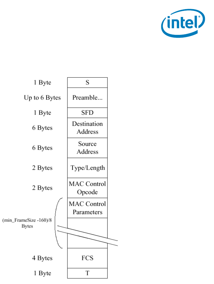
Flow Control — Intel® 82575EB Gigabit Ethernet Controller
324632-003 Intel® 82575EB Gigabit Ethernet Controller
Revision: 2.1 Software Developer’s Manual and EEPROM Guide
January 2011 253
Note: “S” is the Start-of-Packet delimiter and “T” is the first part of the End-of-Packet delimiters for 802.3z encapsulation.
Figure 27. 802.3x MAC Control Frame Format
The receiver is enabled to receive flow control frames if flow control is enabled through the RFCE bit in
the Device Control register (CTRL).
Note: Flow control capability must be negotiated between link partners via the Auto-Negotiation
process. The Auto-Negotiation process can modify the value of these bits based on the
resolved capability between the local device and the link partner.
Once the receiver has validated the reception of an XOFF, or PAUSE frame, the 82575 performs the
following:
• Increment the appropriate statistics register(s)
• Set the TXOFF bit in the Device Status Register (STATUS)
• Initialize the pause timer based on the packet’s PAUSE timer field
• Disable packet transmission or schedule the disabling of transmission after the current packet
completes.

Intel® 82575EB Gigabit Ethernet Controller — Discard PAUSE Frames and Pass MAC Control
Frames
Intel® 82575EB Gigabit Ethernet Controller 324632-003
Software Developer’s Manual and EEPROM Guide Revision: 2.1
254 January 2011
Resumption of transmission can occur under the following conditions:
• Expiration of the PAUSE timer
• Reception of on XON frame (a frame with its PAUSE timer set to 0b)
Either condition clears the TXOFF status bit in the Device Status Register and transmission might
resume. Hardware records the number of received XON frames.
Note: When flow control reception is disabled (CTRL.RFCE = 0b), flow control packets are not
recognized and are parsed as regular packets.
9.3.5 Discard PAUSE Frames and Pass MAC Control
Frames
Two bits in the Receive Control register (RCTL) are implemented specifically for control over receipt of
PAUSE and MAC control frames. These bits are Discard PAUSE Frames (DPF) and Pass MAC Control
Frames (PMCF). See Section 14.3.47 for DPF and PMCF bit definitions.
The DPF bit forces the discarding of any valid PAUSE frame addressed to the 82575’s station address. If
the packet is a valid PAUSE frame and is addressed to the station address (receive address [0]), the
82575 does not pass the packet to host memory if the DPF bit is set to logic high. When DPF is cleared
to 0b, a valid flow control packet is transferred via DMA. This bit has no affect on PAUSE operation, only
the DMA function.
The PMCF bit allows for the passing of any valid MAC control frames to the system which do not have a
valid PAUSE opcode. In other words, the frame can have the correct MAC control frame multicast
address (or the MAC station address) as well as the correct type field match with the FCT register, but
does not have the defined PAUSE opcode of 0001h. Frames of this type are transferred to host memory
when PMCF is logic high.
9.3.6 Transmission of PAUSE Frames
Transmitting PAUSE frames is enabled by software writing a 1b to the CTRL.TFCE bit.
Similar to the reception flow control packets described earlier, XOFF packets can be transmitted only if
this configuration has been negotiated between the link partners via the Auto-Negotiation process. In
other words, the setting of this bit indicates the desired configuration.
The content of the Flow Control Receive Threshold High register determines at what point hardware
first transmits a PAUSE frame. Hardware monitors the fullness of the receive FIFO and compares it with
the contents of FCRTH. When the threshold is reached, hardware sends a PAUSE frame with its pause
time field equal to FCTTV.
At this time, hardware starts counting an internal shadow counter (reflecting the pause timeout counter
at the partner end) from zero. When the counter reaches the value indicated in FCRTV register, then, if
the PAUSE condition is still valid (meaning that the buffer fullness is still above the low watermark), an
XOFF message is sent again.
Once the receive buffer fullness reaches the low water mark, hardware sends an XON message (a
PAUSE frame with a timer value of 0). Software enables this capability with the XONE field of the
FCRTL.

Software Initiated PAUSE Frame Transmission — Intel® 82575EB Gigabit Ethernet Controller
324632-003 Intel® 82575EB Gigabit Ethernet Controller
Revision: 2.1 Software Developer’s Manual and EEPROM Guide
January 2011 255
Hardware sends a PAUSE frame if it has previously sent one and the FIFO overflows even if the refresh
timer did not expire. This minimizes the amount of packets dropped if the first PAUSE frame did not
reach its target. Since the manageability receive packets use the same data path, the behavior is
identical when manageability packets are received.
Note: Transmitting Flow Control frames should only be enabled in full duplex mode per the IEEE
802.3 standard. Software should ensure that the transmission of flow control packets is
disabled when the 82575 is operating in half-duplex mode.
9.3.7 Software Initiated PAUSE Frame Transmission
The 82575 has the added capability to transmit an XOFF frame through software. This function is
accomplished by software writing a 1b to the SWXOFF bit of the Transmit Control register (TCTL). Once
this bit is set, hardware initiates the transmission of a PAUSE frame in a manner similar to that
automatically generated by hardware.
The SWXOFF bit is self clearing after the PAUSE frame has been transmitted. Note that the Flow Control
Refresh Threshold mechanism does not work in case of software-initiated flow control. As a result, it is
software’s responsibility to re-generate PAUSE frames before expiration of the pause counter at the
other partner’s end.
The state of the CTRL.TFCE bit or the negotiated flow control configuration does not affect software
generated PAUSE frame transmission.
Note: Software sends an XON frame by programming a 0b in the PAUSE timer field of the FCTTV
register. The software emission of XON packet is not allowed while the hardware flow
control mechanism is active, as both use the FCTIV registers for different purposes.
• XOFF transmission is not supported in 802.3x for half duplex links. Software should not initiate an
XOFF or XON transmission if the 82575 is configured for half duplex operation.
• When flow control is disabled, pause packets (XON/XOFF/other FC) are not detected as Flow
Control packets and can be counted in all kinds of counters (for example, multicast).
9.4 Loopback Support
The 82575 supports four types of loopback in the LAN interfaces:
• MAC Loopback (Point 1)
• Internal PHY Loopback (Point 2)
• Internal SerDes Loopback (Point 3)
• External PHY Loopback (Point 4)
By setting the 82575 to loopback mode, packets that are transmitted towards the line are looped back
to the host. The 82575 is fully functional in these modes, just not transmitting data over the lines.
Figure 28 shows the points of loopback.
Note: For more details about loopback usage and test setup, refer to the Intel® Ethernet
Controllers Loopback Modes application note.
Intel® 82575EB Gigabit Ethernet Controller — MAC Loopback
Intel® 82575EB Gigabit Ethernet Controller 324632-003
Software Developer’s Manual and EEPROM Guide Revision: 2.1
256 January 2011
Figure 28. 82575 Loopback Modes
9.4.1 MAC Loopback
In MAC loopback, the PHY and SerDes blocks are not functional and data is looped back before these
blocks. MAC loopback is operational only when operating in PHY mode (CTRL_EXT.LINK_MODE = 00b).
9.4.1.1 Setting the 82575 to MAC Loopback Mode
The following procedure should be used to place the 82575 in MAC loopback mode:
• Set RCTL.LBM to 01b (bits 7:6)
• Set CTRL.SLU (bit 6; should be set by default)
• Set CTRL.FRCSPD and FRCDPLX (bits 11 and 12)
• Set CTRL.SPEED to 10b (1 Gb/s) and CTRL.FD
• Set CTRL.ILOS.
Filter configuration and other TX/RX processes are as the same as I n normal mode.
Note: This configuration can be used when there is no link in the PHY. If there is a link then the
ILOS bit should be cleared.
9.4.2 Internal PHY Loopback
In internal PHY loopback, the SerDes block is not functional and data is looped back at the end of the
PHY functionality. This means that the only design that is functional in copper mode is involved in the
loopback.
9.4.2.1 Setting the 82575 to Internal PHY Loopback Mode
The following procedure should be used to put the 82575 in internal PHY loopback mode:
• Set Link mode to PHY: CTRL_EXT.LINK_MODE (CSR 18h, bits 23:22) = 00b
• In the PHY control register (address 0 in the PHY):
— Set duplex mode (bit 8)
MAC
Packet Buffer
and DMA
SerDes
Interface
Internal
PHY
GMII
PCIe
SerDes
SGMII
1GbT
2
3
4
1

Internal SerDes Loopback — Intel® 82575EB Gigabit Ethernet Controller
324632-003 Intel® 82575EB Gigabit Ethernet Controller
Revision: 2.1 Software Developer’s Manual and EEPROM Guide
January 2011 257
— Clear the Loopback bit (bit 14)
— Set the Auto Neg Enable bit (bit 12)
— Register values should be:
a. For 10 Mb/s 4100h.
b. For 100 Mb/s 6100h.
c. For 1000 Mb/s 4140h.
d. In the Port Control register, address 16 (10h) in the PHY, set bit 14 (Link Disable). This is not
required for 1 Gb/s but required for 10/100 Mb/s.
9.4.3 Internal SerDes Loopback
In internal SerDes loopback, the PHY block is not functional and data is looped back at the end of the
SerDes functionality. This means that the only design that is functional in SerDes/SGMII mode is
involved in the loopback.
9.4.3.1 Setting Internal SerDes Loopback Mode
The following procedure should be used to put the 82575 in SerDes loopback mode:
• Set link mode to SerDes: CTRL_EXT.LINK_MODE (CSR 18h, bits 23:22) = 11b
• Configure the SerDes (register 4, bit 1) to loopback: write to SERDESCTL (CSR 00024h) the value
410h
• Move to force mode by setting the following bits:
— CTRL.FD (CSR 0h, bit 0) = 1b
— CTRL.SLU (CSR 0h, bit 6) = 1b
— CTRL.RFCE (CSR 0h, bit 27) = 0b
— CTRL.TFCE (CSR 0h, bit 28) = 0b
— CTRL.LRST (CSR 0h, bit 3) = 0b
— PCS_LCTL.FORCE_LINK (CSR 04208h, bit 5) = 1b
— PCS_LCTL.FSD (CSR 04208h, bit 4) = 1b
— PCS_LCTL.FDV (CSR 04208h, bit 3) = 1b
— PCS_LCTL.FLV (CSR 04208h, bit 0) = 1b
— PCS_LCTL.AN_ENABLE (CSR 04208h, bit 16) = 0b
— CONNSW.ENRGSRC (CSR 00034h, bit 2) = 0b
9.4.4 External PHY Loopback
In external PHY loopback, the SerDes block is not functional and data is sent through the MDI interface
and looped back using an external loopback plug. This means that the only design that is functional in
copper mode is involved in the loopback. If connected at 10/100 Mb/s, the loopback operates without
any special setup.

Intel® 82575EB Gigabit Ethernet Controller — External PHY Loopback
Intel® 82575EB Gigabit Ethernet Controller 324632-003
Software Developer’s Manual and EEPROM Guide Revision: 2.1
258 January 2011
9.4.4.1 Setting External PHY Loopback Mode
The following procedure should be used to put the 82575 in external PHY loopback mode:
• Set Link mode to PHY: CTRL_EXT.LINK_MODE (CSR 18h, bits 23:22) = 00b
• In the PHY control register (address 0 in the PHY):
— Set duplex mode (bit 8)
— Clear the Loopback bit (bit 14)
— Set the Auto Neg Enable bit (bit 12)
• Restart auto-negotiation (set bit 19)
• Reset the PHY (set bit 15)
• Wait for auto-negotiation to complete and then transmit and receive normally.
§ §
802.1q VLAN Support — Intel® 82575EB Gigabit Ethernet Controller
324632-003 Intel® 82575EB Gigabit Ethernet Controller
Revision: 2.1 Software Developer’s Manual and EEPROM Guide
January 2011 259
10.0 802.1q VLAN Support
The 82575 provides several specific mechanisms to support 802.1q VLANs:
• Optional adding (for transmits) and stripping (for receives) of IEEE 802.1q VLAN tags
• Optional ability to filter packets belonging to certain 802.1q VLANs
10.1 802.1q VLAN Packet Format
Table 81 compares an untagged 802.3 Ethernet packet with an 802.1q VLAN tagged packet.
Table 81. VLAN Packet Format Comparison
Note: The CRC for the 802.1q tagged frame is re-computed so that it covers the entire tagged
frame including the 802.1q tag header. Also, max frame size for an 802.1q VLAN packet is
1522 octets as opposed to 1518 octets for a normal 802.3z Ethernet packet.
10.1.1 802.1q Tagged Frames
For 802.1q, the Tag Header field consists of four octets comprised of the Tag Protocol Identifier (TPID)
and Tag Control Information (TCI), each taking 2 octets. The first 16 bits of the tag header make up the
TPID. It contains the “protocol type” which identifies the packet as a valid 802.1q tagged packet.
The two octets making up the TCI contain three fields (see Table 82 for details):
• User Priority (UP)
• Canonical Form Indicator (CFI). The CFI should be 0b for transmits. For receives, the 82575 has the
capability to filter out packets that have this bit set. See the CFIEN and CFI bits in the RCTL as
described in Section 14.3.47.
• VLAN Identifier (VID)
802.3 Packet #Octets 802.1q VLAN Packet #Octets
DA 6 DA 6
SA 6 SA 6
Type/Length 2 8021.q Tag 4
Data 46-1500 Type/Length 2
CRC 4 Data 46-1500
CRC* 4

Intel® 82575EB Gigabit Ethernet Controller — Transmitting and Receiving 802.1q Packets
Intel® 82575EB Gigabit Ethernet Controller 324632-003
Software Developer’s Manual and EEPROM Guide Revision: 2.1
260 January 2011
Table 82. 802.1q Tagged Frames
10.2 Transmitting and Receiving 802.1q
Packets
Since the 802.1q tag is only four bytes, adding and stripping of tags can done completely in software.
(For transmits, software inserts the tag into packet data before it builds the transmit descriptor list, and
for receives, software strips the four byte tag from the packet data before delivering the packet to
upper layer software.)
However, because adding and stripping of tags in software results in more overhead for the host, the
82575 has additional capabilities to add and strip tags in hardware, as discussed in the following two
sections.
10.2.1 Adding 802.1q Tags on Transmits
Software might command the 82575 to insert an 802.1q VLAN tag on a per packet or per flow basis. If
CTRL.VME is set to 1b, and the VLE bit in the transmit descriptor is set to 1b, then the 82575 inserts a
VLAN tag into the packet that it transmits over the wire. The Tag Protocol Identifier (TPID) field of the
802.1q tag comes from the VET register. 8021.Q tag insertion is done in different ways for legacy and
advanced Tx descriptors:
• Legacy Transmit Descriptors: The Tag Control Information (TCI) of the 802.1q tag comes from the
VLAN field (Section 5.3.3.5) of the descriptor. Refer to Table 83 for more on hardware insertion of
tags for transmits.
• Advanced Transmit Descriptor: The Tag Control Information (TCI) of the 802.1q tag comes from the
VLAN Tag field (Section 5.3.3.5) of the advanced context descriptor. The IDX field of the advanced
Tx descriptor should be set to the adequate context can result in unexpected behavior.
Octet 1 Octet 2
UP CF
I
VID
Table 83. VLAN Tag Insertion Decision Table
VLE Action
0b Send generic Ethernet packet.
1b Send 802.1Q packet; the Ethernet Type field comes from the VET register and the VLAN data comes from the
VLAN field of the TX descriptor;
Note: This table is relevant only if VMVIR.VLANA = 00b (use descriptor command) for the queue.

Stripping 802.1q Tags on Receives — Intel® 82575EB Gigabit Ethernet Controller
324632-003 Intel® 82575EB Gigabit Ethernet Controller
Revision: 2.1 Software Developer’s Manual and EEPROM Guide
January 2011 261
10.2.2 Stripping 802.1q Tags on Receives
Software can instruct the 82575 to strip 802.1q VLAN tags from received packets. If the CTRL.VME bit
is set to 1b, and the incoming packet is an 802.1q VLAN packet (its Ethernet Type field matched the
VET register), then the 82575 strips the 4-byte VLAN tag from the packet, and stores the TCI in the
Special field of the receive descriptor.
The 82575 also sets the VP bit in the receive descriptor to indicate that the packet had a VLAN tag that
was stripped. If the CTRL.VME bit is not set, the 802.1Q packets can still be received if they pass the
receive filter. In this case, the VLAN tag is not stripped and the VP bit is not set. Refer to Table 84 for
more information regarding receive packet filtering.
10.3 802.1q VLAN Packet Filtering
VLAN filtering is enabled by setting the RCTL.VFE bit to 1b. If enabled, hardware compares the type
field of the incoming packet to a 16-bit field in the VLAN EtherType (VET) register. If the VLAN type field
in the incoming packet matches the VET register, the 802.1q VLAN packet is then compared against the
VLAN Filter Table Array for acceptance.
The Virtual LAN ID field indexes a 4096 bit vector. If the indexed bit in the vector is 1b, there is a Virtual
LAN match. Software can set the entire bit vector to 1b’s if the node does not implement 802.1q
filtering.
In summary, the 4096 bit vector is comprised of 128 32-bit registers. The VLAN Identifier (VID) field
consists of 12 bits. The upper 7 bits of this field are decoded to determine the 32-bit register in the
VLAN Filter Table Array to address and the lower 5 bits determine which of the 32 bits in the register to
evaluate for matching.
Two other bits in the Receive Control register (see Section 14.3.47), CFIEN and CFI, are also used in
conjunction with 802.1q VLAN filtering operations. CFIEN enables the comparison of the value of the
CFI bit in the 802.1q packet to the Receive Control register CFI bit as an acceptance criteria for the
packet.
Table 84 lists reception actions according to control bit settings.
Note: The VFE bit does not affect whether the VLAN tag is stripped. It only affects whether the
VLAN packet passes the receive filter.
A packet is defined as a VLAN/802.1q packet if its type field matches the VET.

Intel® 82575EB Gigabit Ethernet Controller — Double VLAN Support
Intel® 82575EB Gigabit Ethernet Controller 324632-003
Software Developer’s Manual and EEPROM Guide Revision: 2.1
262 January 2011
Table 84. Packet Reception Decision Table
10.4 Double VLAN Support
The 82575 supports a mode where all received and sent packet have at least one VLAN tag in addition
to the regular tagging which may optionally be added. This mode is used for systems where the
switches add an additional tag containing switching information.
When a port of the 82575 is working in this mode, the 82575 assumes that all packets received or sent
to this port have at least one VLAN, including packet received or sent on the NC-SI interface.
One exception to this rule are flow control PAUSE packets which are not expected to have any VLAN.
Insertion or stripping of VLAN is done on the second VLAN if it exists. All the filtering functions of the
82575 (Rx filtering) ignores the first VLAN in this mode.
This mode is activated by setting CTRL_EXT.EXTENDED_VLAN bit. The default of this bit is set according
to bit 1 in word 24h/14h of the EEPROM for ports 0 and 1, respectively.
The type of the VLAN tag used for the additional VLAN is defined in the VET.VET_EXT field.
The Rx filter detects the presence of this VLAN and indicates it in the RDESC.STATUS.VEXT bit.
§ §
Is packet
802.1q? CTRL.
VME RCTL.
VFE Action
No X X Normal packet reception.
Yes 0 0 Receive a VLAN packet if it passes the standard filters (only). Leave the packet as
received in the data buffer. Clear the VP bit in the receive descriptor.
Yes 0 1 Receive a VLAN packet if it passes the standard filters and the VLAN filter table. Leave
the packet as received in the data buffer (the VLAN tag is not stripped). Clear the VP
bit in the receive descriptor.
Yes 1 0 Receive a VLAN packet if it passes the standard filters (only). Strip off the VLAN
information (four bytes) from the incoming packet and store in the descriptor. Set the
VP bit in the receive descriptor.
Yes 1 1 Receive a VLAN packet if it passes the standard filters and the VLAN filter table. Strip
off the VLAN information (four bytes) from the incoming packet and store in the
descriptor. Set the VP bit in the receive descriptor.

PHY Functionality and Features — Intel® 82575EB Gigabit Ethernet Controller
324632-003 Intel® 82575EB Gigabit Ethernet Controller
Revision: 2.1 Software Developer’s Manual and EEPROM Guide
January 2011 263
11.0 PHY Functionality and Features
The PHY default configuration is determined by data from the EEPROM, read right after power-on reset.
11.1 Auto MDIO Register Initialization
The 82575 PHYs support an option for automatically initializing MDIO registers with values from
EEPROM/ROM, in case defaults in hardware are not adequate. In the 82575, this is performed by
firmware.
There are two types of register initialization:
1. General register initialization - any register in a PHY can be initialized.
2. Customer visible mirror bit initialization - there are some bits in PHY that are a mirror of a customer
visible EEPROM bits (PHY register 25 bits 3:0 and 6 and PHY register 26 bit 0).
After any PHY reset (power down included), a PHY needs to be initialized.
The register initialization is done by the firmware through the MAC/PHY MDIO interface (MDIC).
11.1.1 General Register Initialization
A block of data is allocated in EEPROM/ROM. This block holds register addresses and data in MDIC
format.
Each time a PHY reset ends, this block is read from EEPROM /ROM (first from ROM then from EEPROM)
by firmware and is written to the PHY registers through the MDIC register and MDIO interface.
11.1.2 Visible Mirror Bit Initialization
There are a number of visible bits that reside in the EEPROM/MAC control registers that have a mirror
bit in the PHY registers. These bits are also updated by firmware after every PHY reset.
These bits are updated after the General Register initialization and through a read modify write
sequence.
The current visible mirror bits are in PHY register 25 (bits 3:0 and bit 6) and PHY register 26 (bit 0).
The PHY might perform some low level initialization such as DSP configuration based on EEPROM
settings. The details of those initialization are beyond the scope of this Software Developers Manual.
Intel® 82575EB Gigabit Ethernet Controller — Determining Link State
Intel® 82575EB Gigabit Ethernet Controller 324632-003
Software Developer’s Manual and EEPROM Guide Revision: 2.1
264 January 2011
11.2 Determining Link State
The PHY and its link partner determine the type of link established through one of three methods:
• Auto-Negotiation
• Parallel Detection
• Forced Operation
Auto-Negotiation is the only method allowed by the 802.3ab standard for establishing a 1000BASE-T
link, although forced operation could be used for test purposes. For 10/100 links, any of the three
methods can be used. The sections that follow discuss each in greater detail.
Figure 29 provides an overview of link establishment. First the PHY checks if Auto-Negotiation is
enabled. By default, the PHY supports Auto-Negotiation (PHY register 0, bit 12). If not, the PHY forces
operation as directed. If Auto-Negotiation is enabled, the PHY begins transmitting Fast Link Pulses
(FLPs) and receiving FLPs from its link partner. If FLPs are received by the PHY, Auto-Negotiation
proceeds. It also can receive 100BASE-TX MLT3 and 10BASE-T Normal Link Pulses (NLPs). If either
MLT3 or NLPs are received, it aborts FLP transmission and immediately brings up the corresponding
half-duplex link.
Figure 29. Overview of Link Establishment
11.2.1 False Link
The PHY does not falsely establish link with a partner operating at a different speed. For example, the
PHY does not establish a 1000 Mb/s or 10 Mb/s link with a 100 Mb/s link partner.
Power-Up, Reset,
Link Failure
Start
A/N
Enabled
?
Speed
0.13
?
No Send FLP
Send NLP
0 = 10M
Send IDLES
1 = 100M
Detect
10Mbps
?
Link
Down
No
Link
Up
Yes
Detect
10Mbps
?
Take
Link
Down
No
Take
Link
Up
Yes
Detect
FLP
Auto
Negotiate
Detect
IDLES
Detect
NLP
10M
Half-Duplex
Link
Yes
No
Parallel
Detect
100M
Half-Duplex
Link
Yes
No Yes
Yes

Forced Operation — Intel® 82575EB Gigabit Ethernet Controller
324632-003 Intel® 82575EB Gigabit Ethernet Controller
Revision: 2.1 Software Developer’s Manual and EEPROM Guide
January 2011 265
When the PHY is first powered on, reset, or encounters a link down state, it must determine the line
speed and operating conditions to use for the network link.
The PHY first checks the MDIO registers (initialized via the Hardware Control Interface or written by
software) for operating instructions. Using these mechanisms, programmers can command the PHY to
do one of the following:
• Force twisted-pair link operation to:
— 1000-T Full Duplex
— 1000-T Half Duplex
— 100-TX, Full Duplex
— 100-TX, Half Duplex
— 10BASE-T, Full Duplex
— 10BASE-T, Half Duplex
• Allow Auto-Negotiation/parallel-detection.
In the first six cases (forced operation), the PHY immediately begins operating the network interface as
commanded. In the last case, the PHY begins the Auto-Negotiation/parallel-detection process.
11.2.2 Forced Operation
Forced operation can be used to establish 10 and 100 links, and 1000 links for test purposes. In this
method, Auto-Negotiation is disabled completely and the link state of the PHY is determined by PHY
register 0d.
Note: When speed is forced, the MDI/MDI-X crossover feature is not functional.
In forced operation, the programmer sets the link speed (10, 100, or 1000) and duplex state (full or
half). For Gigabit (1000) links, the programmer must explicitly designate one side as the Master and
the other as the Slave. Table 85 summarizes link establishment procedures.
11.2.3 Auto Negotiation
The PHY supports the IEEE 802.3u Auto-Negotiation scheme with next page capability. Next Page
exchange uses PHY register 7d to send information and PHY register 8d to receive them. Next Page
exchange can only occur if both ends of the link advertise their ability to exchange Next Pages.
Table 85. Determining Duplex State Via Parallel Detection
Configuration Result
Both sides set for Auto-Negotiate. Link is established via Auto-Negotiation.
Both sides set for forced operation. No problem as long as duplex settings match.
One side set for Auto-Negotiation and the other for forced,
half-duplex.
Link is established via parallel detect.
One side set for Auto-Negotiation and the other for forced full-
duplex.
Link is established; however, sides disagree, resulting in
transmission problems. Forced side is full-duplex, Auto-
Negotiation side is half-duplex.

Intel® 82575EB Gigabit Ethernet Controller — Parallel Detection
Intel® 82575EB Gigabit Ethernet Controller 324632-003
Software Developer’s Manual and EEPROM Guide Revision: 2.1
266 January 2011
11.2.4 Parallel Detection
Parallel detection can only be used to establish 10 and 100 links. It occurs when the PHY tries to
negotiate (transmit FLPs to its link partner), but instead of sensing FLPs from the link partner, it senses
100BASE-TX MLT3 code or 10BASE-T Normal Link Pulses (NLPs) instead. In this case, the PHY
immediately stops Auto-Negotiation (terminates transmission of FLPs) and immediately brings up
whatever link corresponds to what it has sensed (MLT3 or NLPs). If the PHY senses both of the
technologies together, a parallel detection fault is detected and the PHY continues sending FLPs
With parallel detection, it is impossible to determine the true duplex state of the link partner, and the
IEEE standard requires the PHY to assume a half-duplex link. Parallel detection also does not allow
exchange of flow-control ability (PAUSE and ASM_DIR) or Master/Slave relationship required by
1000BASE-T. For this reason, parallel detection cannot be used to establish Gigabit Ethernet links.
11.2.5 Auto Cross-Over
Twisted pair Ethernet PHY's must be correctly configured for MDI or MDI-X operation to interoperate.
The PHY supports the automatic MDI/MDI-X configuration originally developed for 1000Base-T and
standardized in IEEE 802.3u section 40. Manual (non-automatic) configuration is still possible.
For 1000BASE-T links, pair identification is determined automatically in accordance with the standard.
For 10/100 links and during auto-negotiation, pair usage is determined by bits 12 and 13 in the PHY
Port Control Register (18d).
In addition, the PHY has an Automatic Crossover Detection function. If bit 12 in PHY register 18d = 1b,
the PHY automatically detects which application is being used and configures itself accordingly.
11.2.5.1 Support for Different Board Layouts
In order to support different board layouts, the 82575 supports an internal flip of the lanes.
The following table lists the logical assignment of the physical lanes in each mode:
The default mode is non-flip chip and auto-MDI-X. For example, MDI or MDI-X mode is set during the
auto-negotiation process (as described in IEEE 802.3, section 40.4.4 Automatic MDI/MDI-X
Configuration).
Flip Chip Non-Flip Chip
MDI Mode A d
B c
C b
D a
A a
B b
C c
D d
MDI-X Mode A c
B d
C a
D b
A b
B a
C d
D c

Link Criteria — Intel® 82575EB Gigabit Ethernet Controller
324632-003 Intel® 82575EB Gigabit Ethernet Controller
Revision: 2.1 Software Developer’s Manual and EEPROM Guide
January 2011 267
11.3 Link Criteria
Once the link state is determined—via Auto-Negotiation, parallel detection or forced operation— the
PHY and its link partner bring up the link.
11.3.1 1000BASE-T
For 1000BASE-T links, the PHY and its link partner enter a training phase. They exchange idle symbols
and use the information gained to set their adaptive filter coefficients.
Either side indicates completion of the training phase to its link partner by changing the encoding of the
idle symbols it transmits. When both sides so indicate, the link is up. Each side continues sending idle
symbols whenever it has no data to transmit. The link is maintained as long as valid idle or data
symbols are received.
11.3.2 100BASE-TX
For 100BASE-TX links, the PHY and its link partner immediately begin transmitting idle symbols. Each
side continues sending idle symbols whenever it has no data to transmit. The link is maintained as long
as valid idle symbols or data is received.
In 100 Mb/s mode, the PHY establishes a link whenever the scrambler becomes locked and remains
locked. Link will remain up unless the descrambler receives idles at less than a specified rate.
11.3.3 10BASE-T
For 10BASE-T links, the PHY and its link partner begin exchanging Normal Link Pulses (NLPs). The PHY
transmits an NLP every 16 ms, and expects to receive one every 10 to 20 ms. The link is maintained as
long as normal link pulses are received.
11.4 Link Enhancements
The PHY offers two enhanced link functions, each of which are discussed in the sections that follow:
• SmartSpeed
• Flow Control
11.4.1 SmartSpeed
SmartSpeed is an enhancement to auto-negotiation that enables the PHY to react intelligently to
network conditions that prohibit establishment of a 1000BASE-T link, such as cable problems. Such
problems might allow auto-negotiation to complete, but then inhibit completion of the training phase.
Normally, if a 1000BASE-T link fails, the PHY returns to the auto-negotiation state with the same speed
settings indefinitely. With SmartSpeed enabled, after a configurable number (1-5, PHY Register 27d bits
8:6) of failed attempts, the PHY automatically downgrades the highest ability it advertises to the next

Intel® 82575EB Gigabit Ethernet Controller — Flow Control
Intel® 82575EB Gigabit Ethernet Controller 324632-003
Software Developer’s Manual and EEPROM Guide Revision: 2.1
268 January 2011
lower speed: from 1000 to 100 to 10. Once a link is established, and if it is later broken, the PHY
automatically upgrades the capabilities advertised to the original setting. This allows the PHY to
automatically recover once the cable plant is repaired.
11.4.1.1 Using SmartSpeed
SmartSpeed is enabled by setting PHY register 16d, bit 7 to 1b. When SmartSpeed downgrades the PHY
advertised capabilities, it sets bit 5 of PHY register 19. When link is established, its speed is indicated in
PHY register 17, bits 15:14. SmartSpeed automatically resets the highest-level Auto-Negotiation
abilities advertised, if link is established and then lost for more than two seconds.
11.4.2 Flow Control
Flow control enables congested nodes to pause traffic. MACs indicate their ability to implement flow
control during Auto-Negotiation.
The PHY transparently supports MAC-to-MAC advertisement of flow control through its Auto-Negotiation
process. Prior to Auto-Negotiation, the MAC indicates its flow control capabilities via PHY register 4d, bit
10 (Pause) and PHY register 4d, bit 11 (ASM_DIR). After Auto-Negotiation, the link partner’s flow
control capabilities are indicated in PHY register 5d, bits 11:10.
Table 86 lists the intended operation for the various settings of ASM_DIR and Pause. This information is
provided for reference only; it is the responsibility of the MAC to implement the correct function. The
PHY merely enables the two MACs to communicate their abilities to each other.
Table 86. Pause And Asymmetric Pause Settings
ASM_DIR Settings Local
(PHY Register 4d, Bit 10)
and Remote (PHY Register
5d, Bit 10)
Pause Setting -
Local (PHY Register
4d, Bit 9)
Pause Setting -
Remote (PHY
Register 5d, Bit 9) Result
Both ASM_DIR = 1b 1b 1b Symmetric - Either side can flow control the
other
1b 0b Asymmetric - Remote can flow control local
only
0b 1b Asymmetric - Local can flow control remote
0b 0b No flow control
Either or both
ASM_DIR = 0b
1b 1b Symmetric - Either side can flow control the
other
Either or both = 0b No flow control

Management Data Interface — Intel® 82575EB Gigabit Ethernet Controller
324632-003 Intel® 82575EB Gigabit Ethernet Controller
Revision: 2.1 Software Developer’s Manual and EEPROM Guide
January 2011 269
11.5 Management Data Interface
The PHY supports the IEEE 802.3 MII Management Interface also known as the Management Data
Input/Output (MDIO) Interface. The MDIO interface consists of a physical connection to the MAC, a
specific protocol which runs across the connection, and a 16-bit MDIO register set.
PHY Registers 0d through 10d and 15d are required and their functions are specified by the IEEE 802.3
specification. Additional registers are included for expanded functionality.
11.6 Low Power Operation
The 82575 can be get into a low-power state according to MAC control (Power Management controls) or
via PHY register 0d. In either power down mode, the 82575 is not capable of receiving or transmitting
packets.
11.7 Power Down via the PHY Register
The PHY can be powered down using the control bit found in PHY register 0d, bit 11. This bit powers
down a significant portion of the port but clocks to the register section remain active. This enables the
PHY management interface to remain active during power-down. The power-down bit is active high.
When the PHY exits software power-down (PHY register 0d, bit 11 = 0b), it re-initializes all analog
functions, but retains its previous configuration settings.
11.8 1000 Mb/s Operation
This section provides an overview of 1000BASE-T functions, followed by discussion and review of the
internal functional blocks shown in Figure 30.
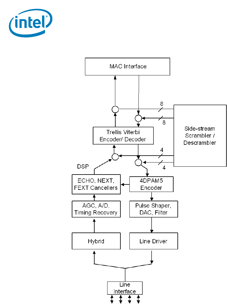
Intel® 82575EB Gigabit Ethernet Controller — Transmit Functions
Intel® 82575EB Gigabit Ethernet Controller 324632-003
Software Developer’s Manual and EEPROM Guide Revision: 2.1
270 January 2011
Figure 30. 1000 Base-T PHY Functions Overview
11.8.1 Transmit Functions
This section describes functions used when the Media Access Controller (MAC) transmits data through
the PHY and out onto the twisted-pair connection.
11.8.1.1 Scrambler
The scrambler randomizes the transmitted data. The purpose of scrambling is two fold:
1. Scrambling eliminates repeating data patterns from the 4DPAM5 waveform to reduce EMI.

Transmit FIFO — Intel® 82575EB Gigabit Ethernet Controller
324632-003 Intel® 82575EB Gigabit Ethernet Controller
Revision: 2.1 Software Developer’s Manual and EEPROM Guide
January 2011 271
2. Each channel (A, B, C, D) gets a unique signature that the receiver uses for identification.
The scrambler is driven by a Linear Feedback Shift Register (LFSR), which is randomly loaded at power-
up. The LFSR function used by the Master differs from that used by the Slave, giving each direction its
own unique signature. The LFSR, in turn, generates uncorrelated outputs. These outputs randomize the
inputs to the 4DPAM5 and Trellis encoders and randomize the sign of the 4DPAM5 outputs.
11.8.2 Transmit FIFO
The transmit FIFO re-synchronizes data transmitted by the MAC to the transmit reference used by the
PHY.
11.8.2.1 Transmit Phase-Locked Loop PLL
This function generates the 125 MHz timing reference used by the PHY to transmit 4DPAM5 symbols.
When the PHY is the Master side of the link, the crystal input is the reference for the transmit PLL.
When the PHY is the Slave side of the link, the recovered receive clock is the reference for the transmit
PLL.
11.8.2.2 Trellis Encoder
The Trellis Encoder uses the two high-order bits of data and its previous output to generate a ninth bit,
which determines if the next 4DPAM5 pattern should be even or odd. This function provides forward
error correction and enhances the signal-to-noise (SNR) ratio by a factor of 6 dB.
11.8.2.3 4DPAM5 Encoder
The 4DPAM5 encoder translates 8B codes transmitted by the MAC into 4DPAM5 symbols. The encoder
operates at 125 Mhz, which is both the frequency of the MAC interface and the baud rate used by
1000BASE-T.
Each 8B code represents one of 256 data patterns. Each 4DPAM5 symbol consists of one of five signal
levels (-2,-1,0,1,2) on each of the four twisted pair (A,B,C,D) representing 54 or 625 possible patterns
per baud period. Of these, 113 patterns are reserved for control codes, leaving 512 patterns for data.
These data patterns are divided into two groups of 256 even and 256 odd data patterns. As a result,
each 8B octet has two possible 4DPAM5 representations—one even and one odd pattern.
11.8.2.4 Spectral Shaper
This function causes the 4DPAM5 waveform to have a spectral signature that is very close to that of the
MLT3 waveform used by 100BASE-TX. This enables 1000BASE-T to take advantage of infrastructure
(cables, magnetics) designed for 100BASE-TX.
The shaper works by transmitting 75% of a 4DPAM5 code in the current baud period, and adding the
remaining 25% into the next baud period.
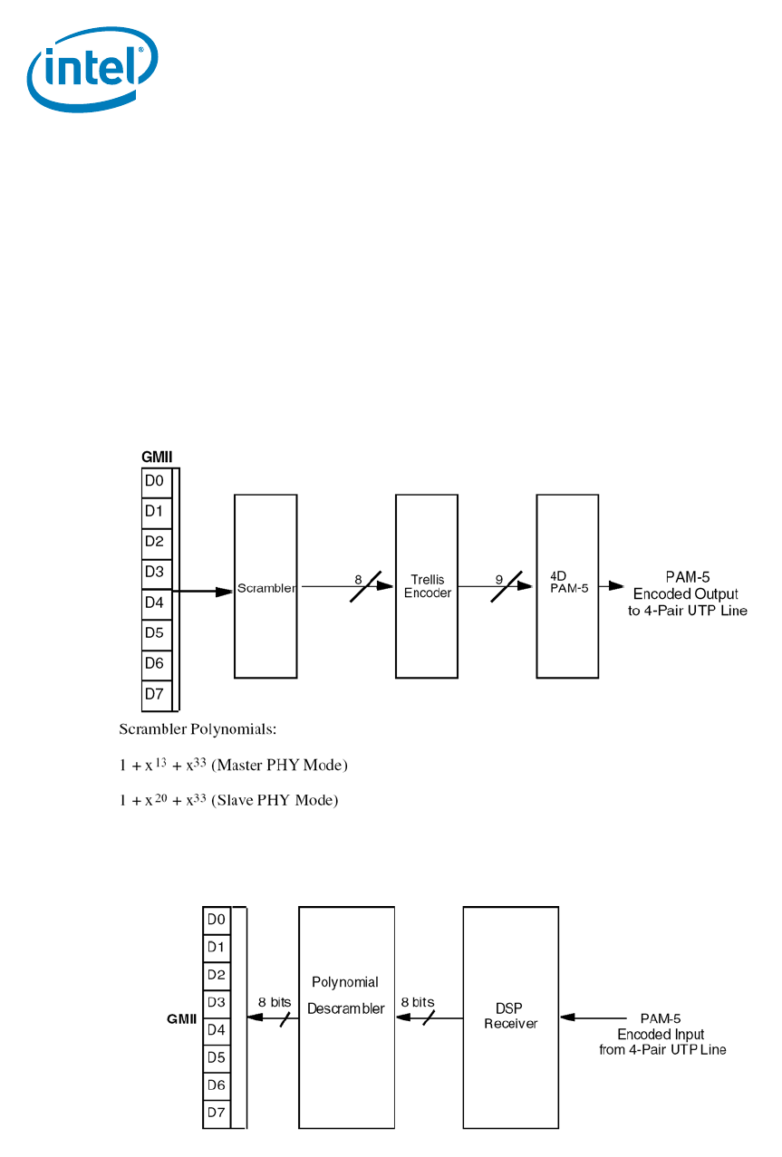
Intel® 82575EB Gigabit Ethernet Controller — Transmit FIFO
Intel® 82575EB Gigabit Ethernet Controller 324632-003
Software Developer’s Manual and EEPROM Guide Revision: 2.1
272 January 2011
11.8.2.5 Low-Pass Filter
To aid with EMI, this filter attenuates signal components more than 180 Mhz. In 1000BASE-T, the
fundamental symbol rate is 125 Mhz.
11.8.2.6 Line Driver
The line driver drives the 4DPAM5 waveforms onto the four twisted-pair channels (A, B, C, D), adding
them onto the waveforms that are simultaneously being received from the link partner.
11.8.2.7 Transmit/Receive Flow
Figure 31. 1000BASE-T Transmit Flow And Line Coding Scheme
Figure 32. 1000BASE-T Receive Flow

Receive Functions — Intel® 82575EB Gigabit Ethernet Controller
324632-003 Intel® 82575EB Gigabit Ethernet Controller
Revision: 2.1 Software Developer’s Manual and EEPROM Guide
January 2011 273
11.8.3 Receive Functions
This section describes function blocks that are used when the PHY receives data from the twisted pair
interface and passes it back to the MAC.
11.8.3.1 Hybrid
The hybrid subtracts the transmitted signal from the input signal, allowing the use of simple 100BASE-
TX compatible magnetics.
11.8.3.2 Automatic Gain Control
The Automatic Gain Control (AGC) normalizes the amplitude of the received signal, adjusting for the
attenuation produced by the cable.
11.8.3.3 Timing Recovery
This function re-generates a receive clock from the incoming data stream which is used to sample the
data. On the Slave side of the link, this clock is also used to drive the transmitter.
11.8.3.4 Analog-to-Digital Converter
The Analog-to-Digital (ADC) function converts the incoming data stream from an analog waveform to
digitized samples for processing by the DSP core.
11.8.3.5 Digital Signal Processor
The Digital Signal Processor (DSP) provides per-channel adaptive filtering, which eliminates various
signal impairments including:
• Inter-symbol interference (equalization).
• Echo caused by impedance mismatch of the cable.
• Near-end crosstalk (NEXT) between adjacent channels (A, B, C, D).
• Far-end crosstalk (FEXT)
• Propagation delay variations between channels of up to 120 ns.
• Extraneous tones that have been coupled into the receive path.
The adaptive filter coefficients are initially set during the training phase. They are continuously adjusted
(adaptive equalization) during operation through the decision-feedback loop.
11.8.3.6 Descrambler
The descrambler identifies each channel by its characteristic signature, removing the signature and re-
routing the channel internally. In this way, the receiver can correct for channel swaps and polarity
reversals. The descrambler uses the same base LFSR used by the transmitter on the other side of the
link.

Intel® 82575EB Gigabit Ethernet Controller — 100 Mb/s Operation
Intel® 82575EB Gigabit Ethernet Controller 324632-003
Software Developer’s Manual and EEPROM Guide Revision: 2.1
274 January 2011
The descrambler requires approximately 15 s. to lock, normally accomplished during the training
phase.
11.8.3.7 Viterbi Decoder/Decision Feedback Equalizer (DFE)
The Viterbi decoder generates clean 4DPAM5 symbols from the output of the DSP. The decoder includes
a Trellis encoder identical to the one used by the transmitter. The Viterbi decoder simultaneously looks
at the received data over several baud periods. For each baud period, it predicts whether the symbol
received should be even or odd, and compares that to the actual symbol received. The 4DPAM5 code is
organized in such a way that a single level error on any channel changes an even code to an odd one
and vice versa. In this way, the Viterbi decoder can detect single-level coding errors, effectively
improving the Signal-To-Noise (SNR). When an error occurs, this information is quickly fed back into
the equalizer to prevent future errors.
11.8.3.8 4DPAM5 Decoder
The 4DPAM5 decoder generates 8B data from the output of the Viterbi decoder.
11.9 100 Mb/s Operation
The MAC passes data to the PHY over the MII. The PHY encodes and scrambles the data, then transmits
it using MLT-3 for 100TX over copper. The PHY descrambles and decodes MLT-3 data received from the
network. When the MAC is not actively transmitting data, the PHY sends out idle symbols on the line.
11.10 10 Mb/s Operation
The PHY operates as a standard 10 Mb/s transceiver. Data transmitted by the MAC as 4-bit nibbles is
serialized, Manchester-encoded, and transmitted on the MDI[0]+/- outputs. Received data is decoded,
de-serialized into 4-bit nibbles and passed to the MAC across the internal MII. The PHY supports all the
standard 10 Mb/s functions.
11.10.1 Link Test
In 10 Mb/s mode, the PHY always transmits link pulses. If the Link Test Function is enabled, it monitors
the connection for link pulses. Once it detects 2 to 7 link pulses, data transmission is enabled and
remains enabled as long as the link pulses or data reception continues. If the link pulses stop, the data
transmission is disabled.
If the Link Test function is disabled, the PHY might transmit packets regardless of detected link pulses.
Setting PHY register 16d, bit 14 can disable the Link Test function.

10Base-T Link Failure Criteria and Override — Intel® 82575EB Gigabit Ethernet Controller
324632-003 Intel® 82575EB Gigabit Ethernet Controller
Revision: 2.1 Software Developer’s Manual and EEPROM Guide
January 2011 275
11.10.2 10Base-T Link Failure Criteria and Override
Link failure occurs if Link Test is enabled and link pulses stop being received. If this condition occurs,
the PHY returns to the Auto-Negotiation phase if Auto-Negotiation is enabled. Setting PHY register 16d,
bit 14 disables the Link Integrity Test function, then the PHY transmits packets, regardless of link
status.
11.10.3 Jabber
If the MAC begins a transmission that exceeds the jabber timer, the PHY disables the transmit and
loopback functions and asserts collision indication to the MAC. The PHY automatically exits jabber mode
after 250-750 ms. This function can be disabled by setting PHY register 16d, bit 10 to 1b.
11.10.4 Polarity Correction
The PHY automatically detects and corrects for the condition where the receive signal (MDI_PLUS[0]/
MDI_MINUS[0]) is inverted. Reversed polarity is detected if eight inverted link pulses, or four inverted
end-of-frame markers, are received consecutively. If link pulses or data are not received for 96-130 ms,
the polarity state is reset to a non-inverted state.
11.10.5 Dribble Bits
The PHY device handles dribble bits for all of its modes. If between one to four dribble bits are received,
the nibble is passed across the interface. The data passed across is padded with 1b’s if necessary. If
between five to seven dribble bits are received, the second nibble is not sent onto the internal MII bus
to the MAC. This ensures that dribble bits between 1-7 do not cause the MAC to discard the frame due
to a CRC error.
§ §

Intel® 82575EB Gigabit Ethernet Controller — Dribble Bits
Intel® 82575EB Gigabit Ethernet Controller 324632-003
Software Developer’s Manual and EEPROM Guide Revision: 2.1
276 January 2011
NOTE: This page intentionally left blank.

Configurable LED Outputs — Intel® 82575EB Gigabit Ethernet Controller
324632-003 Intel® 82575EB Gigabit Ethernet Controller
Revision: 2.1 Software Developer’s Manual and EEPROM Guide
January 2011 277
12.0 Configurable LED Outputs
The 82575 implements four output drivers intended for driving external LED circuits per port. Each LAN
device provides an independent set of LED outputs (these pins and their function are bound to a specific
LAN device). Each of the four LED outputs can be individually configured to select the particular event,
state, or activity that is indicated on that output. n addition, each LED can be individually configured for
output polarity as well as for blinking versus non-blinking (steady-state) indication.
The configuration for LED outputs is specified via the LEDCTL register. In addition, the hardware-default
configuration for all the LED outputs can be specified via EEPROM fields, thereby supporting LED
displays configurable to a particular OEM preference.
Each of the four LED’s can be configured to use one of a variety of sources for output indication. The
MODE bits control the LED source:
• LINK_100/1000 is asserted when link is established at either 100 or 1000 Mb/s.
• LINK_10/1000 is asserted when link is established at either 10 or 1000 Mb/s.
• LINK_UP is asserted when any speed link is established and maintained.
• ACTIVITY is asserted when link is established and packets are being transmitted or received.
• LINK/ACTIVITY is asserted when link is established AND there is NO transmit or receive activity
• LINK_10 is asserted when a 10 Mb/s link is established and maintained.
• LINK_100 is asserted when a 100 Mb/s link is established and maintained.
• LINK_1000 is asserted when a 1000 Mb/s link is established and maintained.
• FULL_DUPLEX is asserted when the link is configured for full duplex operation.
• COLLISION is asserted when a collision is observed.
• PAUSED is asserted when the 82575's transmitter is flow controlled.
• LED_ON is always asserted; LED_OFF is always de-asserted.
The IVRT bits enable the LED source to be inverted before being output or observed by the blink-control
logic. LED outputs are assumed to normally be connected to the negative side (cathode) of an external
LED.
The BLINK bits control whether the LED should be blinked (either 200 ms on and 200 ms off or 83 ms
on and 83 ms off) while the LED source is asserted. The blink control might be especially useful for
ensuring that certain events, such as ACTIVITY indication, cause LED transitions, which are sufficiently
visible to a human eye.
Note: The LINK/ACTIVITY source functions slightly different from the others when BLINK is
enabled. The LED is off if there is no LINK, on if there is LINK and no ACTIVITY, and blinking
if there is LINK and ACTIVITY.
§ §

Intel® 82575EB Gigabit Ethernet Controller — Configurable LED Outputs
Intel® 82575EB Gigabit Ethernet Controller 324632-003
Software Developer’s Manual and EEPROM Guide Revision: 2.1
278 January 2011
NOTE: This page intentionally left blank.

Dual Port Characteristics — Intel® 82575EB Gigabit Ethernet Controller
324632-003 Intel® 82575EB Gigabit Ethernet Controller
Revision: 2.1 Software Developer’s Manual and EEPROM Guide
January 2011 279
13.0 Dual Port Characteristics
The 82575 architecture includes two instances both the MAC and PHY. With both MAC/PHY pairs
operating, the 82575 appears as a multi-function PCIe* device containing two identically-functioning
devices. To avoid confusion, each MAC (when combined with either an internal/external PHY or SerDes)
is referred to as “LANx”, where x = “A” or
x = “B” to refer to each logical LAN device (LAN 0 or LAN 1).
This section details specific features common to each MAC or PHY, resources/interfaces for which
dedicated independent hardware/software interfaces exists for each LAN, as well as resources which
are shared by both LAN devices.
The 82575 normally appears to the system as a single, multi-function PCIe* device. It provides the
ability to selectively disable one of the internal LAN functions, thereby allowing it to appear to the
system as a single-function, single-LAN device. The mechanisms for controlling this behavior and the
resulting appearance to the system are described in Section 13.5 entitled, “LAN Disable”.
13.1 Features of Each MAC
The 82575 is designed to have the capability to appear as two independent instances of a gigabit
controller. The following section details major features that can be considered to be distinct features
available to each 82575 MAC independently.
13.1.1 PCIe* Interface
The 82575 contains a single physical PCIe* core interface. The 82575 is designed so that each of the
logical LAN devices (LAN 0, LAN 1) appears as a distinct function implementing, amongst other
registers, the following PCIe* device header space:
Byte Offset Byte 0 Byte 1 Byte 2 Byte 3
0h Device ID Vendor ID
4h Status Register Command Register
8h Class Code 020000h Revision ID (02h)
Ch 00h Header Type 00h Latency Timer Cache Line Size
10h Base Address 0
14h Base Address 1
18h Base Address 2
1Ch Base Address 3
20h Base Address 4
24h Base Address 5

Intel® 82575EB Gigabit Ethernet Controller — PCIe* Interface
Intel® 82575EB Gigabit Ethernet Controller 324632-003
Software Developer’s Manual and EEPROM Guide Revision: 2.1
280 January 2011
Many of the fields of the PCIe* header space contain hardware default values that are either fixed or
can be overridden using EEPROM, but cannot be independently specified for each logical LAN device.
The following fields are considered to be common to both LAN devices:
The following fields are implemented unique to each LAN device:
28h Cardbus CIS Pointer (not used)
2Ch Subsystem ID Subsystem Vendor ID
30h Expansion ROM Base Address
34h Reserved Cap_Ptr
38h Reserved
3Ch Max_Latency 00h Min_Grant
FFh
Interrupt Pin
01h or 02h)
Interrupt Line
00h
Vendor ID Vendor ID is fixed to 8086 and is not readable from EEPROM.
Revision The revision number of the 82575 is reflected identically for both LAN devices.
Header Type This field indicates if a device is single function or multifunction. The value reflected in this field is
reflected identically for both LAN devices, but the actual value reflected depends on LAN Disable
configuration.
When both 82575 LAN ports are enabled, both PCI headers return 80h in this field, acknowledging
being part of a multi-function device. LAN A exists as device “function 0”, while LAN B exists as
device “function 1”.
If one of the LAN ports is disabled, then only a single-function device is indicated (this field returns
a value of 00h), and the LAN exists as device “function 0”.
Subsystem ID The Subsystem ID of the 82575 can be specified via EEPROM, but only a single value can be
specified. The value is reflected identically for both LAN devices.
Subsystem Vendor ID The Subsystem Vendor ID of the 82575 can be specified via EEPROM, but only a single value can
be specified. The value is reflected identically for both LAN devices.
Class Code,
Cap_Ptr,
Max Latency,
Min Grant
These fields reflect fixed values that are constant values reflected for both LAN devices.
Device ID The Device ID reflected for each LAN device can be independently specified via EEPROM.
Command,
Status
Each LAN device implements its own command/status registers.
Latency Timer,
Cache Line Size
Each LAN device implements these registers uniquely. The system should program these fields
identically for each LAN to ensure consistent behavior and performance of each device.
Memory BAR,
Flash BAR,
IO BAR,
Expansion ROM BAR
Each LAN device implements its own Base Address registers, allowing each device to claim its own
address region(s).
Interrupt Pin Each LAN device independently indicates which interrupt pin (INTA# or INTB#) is used by that
82575’s MAC to signal system interrupts. The value for each LAN device can be independently
specified via EEPROM, but only if both LAN devices are enabled.
Byte Offset Byte 0 Byte 1 Byte 2 Byte 3

MAC Configuration Register Space — Intel® 82575EB Gigabit Ethernet Controller
324632-003 Intel® 82575EB Gigabit Ethernet Controller
Revision: 2.1 Software Developer’s Manual and EEPROM Guide
January 2011 281
13.1.2 MAC Configuration Register Space
All device control/status registers detailed in Section 14.3, Main Register Descriptions, are implemented
per-LAN device. Each LAN device can be accessed using memory or I/O cycles, depending on the
specific BAR setting(s) established for that LAN device.
Register accesses to each MAC instance are independent. An outstanding read for one LAN device does
not impact the 82575’s ability to accept a register access to the other LAN. PCIe* bus operation, where
each register access results in a completion by one LAN device, in no way prevents the other LAN
device from accepting and servicing its register space as the 82575’s PCIe* core supports two credits
for memory accesses.
13.1.3 SDP, LED, INT# Output
Each LAN device provides an independent set of LED outputs and software-programmable I/O pins
(SDP). Four LED outputs and four SDP pins are provided per LAN device. These pins and their function
are bound to a specific LAN device (eight SDP pins cannot be associated with a single LAN device, for
example).
13.2 Shared EEPROM
The 82575 uses a single EEPROM device to configure hardware default parameters for both LAN
devices, including Ethernet Individual Addresses (IA), LED behaviors, receive packet-filters for
manageability and wakeup capability, etc. Certain EEPROM words are used to specify hardware
parameters which are LAN device-independent (such as those that affect circuits behavior). Other
EEPROM words are associated with a specific LAN device. LAN 0 and LAN 1 accesses the EEPROM to
obtain their respective configuration settings.
13.3 Shared FLASH
The 82575 provides an interface to an external FLASH/ROM memory device, as described in
Section 4.0. This FLASH/ROM device can be mapped into memory and/or I/O address space for each
LAN device through the use of PCI Base Address Registers (BARs). Bit 3 of the EEPROM Initialization
Control Word 3 associated with each LAN device selectively disables/enables whether the FLASH can be
mapped for each LAN device by controlling the BAR register advertisement and writeability.
13.3.1 FLASH Access Contention
The 82575 implements internal arbitration between Flash accesses initiated through the LAN "A" device
and those initiated through the LAN "B" device. If accesses from both LAN devices are initiated during
the same approximate size window, The first one is served first and only then the next one, Note that
the 82575 does not synchronize between the two entities accessing the Flash though contentions
caused from one entity reading and the other modifying the same locations is possible.

Intel® 82575EB Gigabit Ethernet Controller — Link Mode/Configuration
Intel® 82575EB Gigabit Ethernet Controller 324632-003
Software Developer’s Manual and EEPROM Guide Revision: 2.1
282 January 2011
To avoid this contention, accesses from both LAN devices MUST be synchronized using external
software synchronization of the memory or I/O transactions responsible for the access. It might be
possible to ensure contention-avoidance simply by nature of software sequentially.
13.4 Link Mode/Configuration
The 82575 provides significant amount of flexibility in pairing a LAN device with a particular type of
media (copper or fiber-optic) as well as the specific transceiver/interface used to communicate with the
media. Each MAC, representing a distinct LAN device, can be coupled with an internal copper PHY (the
default) or SerDes interface independently. The link configuration specified for each LAN device can be
specified in the LINK_MODE field of the Extended Device Control Register (CTRL_EXT) and initialized
from the EEPROM Initialization Control Word 3 associated with each LAN device
13.5 LAN Disable
For a LOM design, it might be desirable for the system to provide BIOS-setup capability for selectively
enabling or disabling LOM devices. This might allow an end-user more control over system resource-
management, avoid conflicts with add-in NIC solutions, etc. The 82575 provides support for selectively
enabling or disabling one or both LAN device(s) in the system.
13.5.1 Overview
Device presence (or non-presence) must be established early during BIOS execution in order to ensure
that BIOS resource-allocation (of interrupts, of memory or IO regions) is done according to devices that
are present only. This is frequently accomplished using a BIOS CVDR (Configuration Values Driven on
Reset) mechanism. The 82575 LAN-disable mechanism is implemented in order to be compatible with
such a solution. The 82575 samples two pins (strapping) on PCIe* reset to determine the LAN-enable
configuration. The 82575 also enables the same through EEPROM presetting.
The LAN disabling can be done at two different levels. Either the LAN is disabled completely, or the
function is not apparent on the PCIe* configuration space. In this case, the LAN function is still available
for the manageability accesses. The selection between the two modes is done using the
PHY_in_LAN_disable EEPROM bit.
When a particular LAN is fully disabled, all internal clocks to that LAN are disabled, the 82575 is held in
reset, and the internal PHY for that LAN is powered-down. In both modes, The 82575 does not respond
to PCI configuration cycles, unless it is function #0, in which case, the function presents itself as a
dummy device. Effectively, the LAN device becomes invisible to the system from both a configuration
and power-consumption standpoint.
As mentioned all PCI functions can be enabled or disabled and an additional EEPROM bit (LAN Function
Sel) enables to swap between the two LAN functions.
It is desired to keep all the functions at their respective location, even when other functions are
disabled. If function #0 (either LAN0 or LAN1) is disabled, then it does not disappear from the PCIe*
configuration space. Rather, the function presents itself as a dummy function. The device ID and class

Multi-Function Advertisement — Intel® 82575EB Gigabit Ethernet Controller
324632-003 Intel® 82575EB Gigabit Ethernet Controller
Revision: 2.1 Software Developer’s Manual and EEPROM Guide
January 2011 283
code of this function changes to other values 10A6h and FF00h, respectively. In addition the function
does not require any memory or I/O space and does not require an interrupt line. Also MSI and MSI-X
capability structure does not appear in this mode. Memory, I/O and master enable bits are read only.
13.5.2 Multi-Function Advertisement
If the LAN 1 port is disabled, the 82575 no longer is a multi-function device. It normally reports a 80h
in the PCI Configuration Header field Header Type, indicating multi-function capability. However, if a
LAN ID is disabled, it reports a 0h in this filed to signify single-function capability.
13.5.3 Legacy Interrupt Use
When both LAN devices are enabled, the 82575 can use interrupt pins INTA# to INTC# for interrupt
reporting. The EEPROM Initialization Control Word 3 (bits 12:11) associated with each LAN device
controls which of these interrupts are used for each LAN device. The specific interrupt pin used is
reported in the PCI Configuration Header Interrupt Pin field associated with each LAN device.
However, if either LAN device is disabled, then INTA# must be used for the remaining LAN device,
regardless of the EEPROM configuration. Under these circumstances, the Interrupt Pin field of the PCI
Header always reports a value of 1h, indicating INTA# usage.
13.5.4 Power Reporting
When both LAN devices are enabled, the PCI Power Management Register Block has the capability of
reporting a Common Power value. The Common Power value is reflected in the data field of the PCI
Power Management registers. The value reported as Common Power is specified via EEPROM, and is
reflected in the data field each time the Data_Select field has a value of 8h (8h = Common Power Value
Select).
When only one LAN is enabled and the 82575 appears as a single-function device, the Common Power
value, if selected, reports 0h (undefined value), as Common Power is undefined for a single-function
device.
13.6 Device Disable
For a LOM design, it might be desirable for the system to provide BIOS-setup capability for selectively
enabling or disabling LOM devices. This allows an end-user more control over system resource-
management; avoid conflicts with add-in NIC solutions, etc. The 82575 provides support for selectively
enabling or disabling it.
Note: If the 82575 is configured to provide a 50 MHz NC-SI clock (via the NC-SI Output Clock
EEPROM bit), then the \Device should not be disabled.
Device Disable is initiated by asserting the asynchronous DEV_OFF_N pin. The DEV_OFF_N pin should
always be connected to enable correct device operation.
The EEPROM Device Disable Power Down En bit enables device disable mode (hardware default is that
the mode is disabled).

Intel® 82575EB Gigabit Ethernet Controller — BIOS Handling of Device Disable
Intel® 82575EB Gigabit Ethernet Controller 324632-003
Software Developer’s Manual and EEPROM Guide Revision: 2.1
284 January 2011
While in device disable mode, the PCIe* link is in L3 state. The PHY is in power down mode. Output
buffers are tri-stated.
Asserting or deasserting the PCIe* PE_RST_N does not have any effect while the 82575 is in device
disable mode (for example, the 82575 stays in the respective mode as long as DEV_OFF_N is asserted).
However, the 82575 might momentarily exit the device disable mode from the time PCIe* PE_RST_N is
de-asserted again and until the EEPROM is read.
During power-up, the DEV_OFF_N pin is ignored until the EEPROM is read. From that point, the 82575
might enter Device Disable if DEV_OFF_N is asserted.
Deasserting the DEV_OFF_N pin causes a fundamental reset to the 82575.
Note: The DEV_OFF_N pin should maintain its state during system reset and system sleep states.
It should also insure the proper default value on system power-up. For example, a designer
could use a GPIO pin that defaults to 1b (enable) and is on system suspend power (it
maintains state in S0-S5 ACPI states).
13.6.1 BIOS Handling of Device Disable
1. Assume that following a power up sequence, the DEV_OFF_N signals is driven high (else it is
already disabled).
2. The PCIe* is established following the GIO_PWR_GOOD
3. BIOS recognizes that the entire 82575 should be disabled.
4. The BIOS drives the DEV_OFF_N signal to the low level.
5. As a result, the 82575 samples the DEV_OFF_N signals and enters device disable mode.
6. The BIOS could put the Link in the Electrical IDLE state (at the other end of the PCIe* link) by
clearing the LINK Disable bit in the Link Control Register.
7. Proceed with normal operation
8. Re-enable could be done by driving the DEV_OFF_N signal high, followed later by bus enumeration.
13.7 Copper/Fiber Switch
The 82575 component provides significant amount of flexibility in pairing a LAN device with a particular
type of media (for example, copper or fiber-optic) as well as the specific transceiver/interface used to
communicate with the media. Each MAC, representing a distinct LAN device, can be coupled with an
internal copper PHY (the default) or SerDes interface independently. The link configuration specified for
each LAN device can be specified in the LINK_MODE field of the Extended Device Control Register
(CTRL_EXT) and initialized from the EEPROM Initialization Control Word 3 associated with each LAN
device.
In some applications, software might need to be aware of the presence of a link on the connection not
currently active. In order to supply such an indication, any of the 82575 ports can set the
AUTOSENSE_EN bit in the CONNSW register (address 00034h) in order to enable sensing of the non
active connection activity. When in SerDes detect mode, software should define which indication is used
to detect the energy change in SerDes/SGMII mode. It can be either the external signal detect pin or
the internal signal detect. This is done using the CONNSW.ENRGSRC bit.

Copper/Fiber Switch — Intel® 82575EB Gigabit Ethernet Controller
324632-003 Intel® 82575EB Gigabit Ethernet Controller
Revision: 2.1 Software Developer’s Manual and EEPROM Guide
January 2011 285
Software can then enable the OMED interrupt in ICR in order to get an indication on any detection of
energy in the non active connection.
The following procedure should be followed in order to enable the auto-sense mode:
• SerDes Detect Mode (PHY is active):
1. Set CONNSW.ENRGSRC to determine the sources for the signal detect indication (1b = external
SIG_DET, 0b = internal SerDes electrical idle). The default of this bit is set by the EEPROM.
2. Set CONNSW.AUTOSENSE_EN.
3. When signal is detected on the SerDes link, the 82575 sets the interrupt bit OMED in ICR and if
enabled, issue an interrupt. The CONNSW.AUTOSENSE_EN is cleared unless CONNSW.ASCLR_DIS
is set. In such a case the host driver is responsible for the clearing of the AUTOSENSE_EN bit.
• PHY Detect Mode:
1. Set CONNSW.AUTOSENSE_CONF = 1b.
2. Reset the PHY by assertion and de-assertion of CTRL.PHY_RST.
3. Wait until EEMNGCTL.CFG_DONE is set.
4. Enter the PHY to Link-Disconnect mode by setting PHY register 25 (bit 5) via MDIC register.
5. Set CONNSW.AUTOSENSE_EN = 1b and clear CONNSW.AUTOSENSE_CONF.
6. When signal is detected on the PHY link, the 82575 sets the interrupt bit OMED in ICR and if
enabled, issue an interrupt.
7. The 82575 puts the PHY in power down unless CONNSW.ASCLR_DIS is set. In such a case the host
driver is responsible for the clearing of the AUTOSENSE_EN bit.
According to the result of the interrupt, software can then decide to switch to the other core.
The following procedures needs to be followed to actually switch between the two modes:
• Internal PHY to SerDes Transition:
1. Disable Receiver by clearing RCTL.RXEN.
2. Disable Transmitter by clearing TCTL.EN.
3. Verify that the 82575 has stopped processing outstanding cycles and is idle.
4. Modify LINK mode to SerDes or SGMII by setting CTRL_EXT.LINK_MODE to 10b or 11b,
respectively.
5. Enable/Disable flow control values within the MAC.
6. Set up Tx and Rx queues and enable Tx and Rx processes.
• SerDes to Internal PHY Transition:
1. Disable Receiver by clearing RCTL.RXEN.
2. Disable Transmitter by clearing TCTL.EN.
3. Verify that the 82575 has stopped processing outstanding cycles and is idle.
4. Modify LINK mode to PHY mode by setting CTRL_EXT.LINK_MODE to 00b.
5. Set Link Up indication by setting CTRL.SLU.
6. Reset the PHY by setting CTRL.PHY_RST, waiting 10 ms and clearing CTRL.PHY_RST.
7. Set up PHY with desired auto-negotiation parameters.
8. Set up Tx and Rx queues and enable Tx and Rx processes.
The 82575's link mode is controlled by the Extended Device Control register:

Intel® 82575EB Gigabit Ethernet Controller — Copper/Fiber Switch
Intel® 82575EB Gigabit Ethernet Controller 324632-003
Software Developer’s Manual and EEPROM Guide Revision: 2.1
286 January 2011
CTRL_EXT (00018h) bits 23:22. The default value for the LINK_MODE setting is directly mapped from
the EEPROM's initialization Control Word 3 (bits 1:0). Software can modify the LINK_MODE indication
by writing the corresponding value into this register.
Note:
• Before dynamically cycling a mode, ensure via the software device driver that the current mode of
operation is not in the process of transmitting or receiving data. This is achieved by disabling the
transmitter and receiver, waiting until the 82575 is in an idle state and then beginning the process
for changing the link mode.
• The mode switch in this method, is only valid until the next hardware reset of the 82575. After a
hardware reset, the link mode is restored to the default set by the EEPROM. To get a permanent
change of the link mode, the default in the EEPROM should be changed.
• The auto switch capability can be used in either port independent of the usage of the other port.
§ §

Copper/Fiber Switch — Intel® 82575EB Gigabit Ethernet Controller
324632-003 Intel® 82575EB Gigabit Ethernet Controller
Revision: 2.1 Software Developer’s Manual and EEPROM Guide
January 2011 287
NOTE: This page intentionally left blank.

Intel® 82575EB Gigabit Ethernet Controller — Copper/Fiber Switch
Intel® 82575EB Gigabit Ethernet Controller 324632-003
Software Developer’s Manual and EEPROM Guide Revision: 2.1
288 January 2011

Register Descriptions — Intel® 82575EB Gigabit Ethernet Controller
324632-003 Intel® 82575EB Gigabit Ethernet Controller
Revision: 2.1 Software Developer’s Manual and EEPROM Guide
January 2011 287
14.0 Register Descriptions
This section details the state inside the 82575 that are visible to the programmer. In some cases, it
describes hardware structures invisible to software in order to clarify a concept.
The internal register/memory space is described in the following sections and divided up into the
following categories:
• General
• Interrupt
• MAC Receive
• MAC Transmit
• Statistics
• Wake Up
• PCIe*
• Diagnostics (including packet buffer memory access)
• Packet Generator
• PHY Receive, Transmit and Special Function
Note: The PHY registers are accessed through the MDI/O interface (see Section 14.3.8 for PHY
register descriptions).
The 82575’s address space is mapped into five regions with PCI Base Address Registers described in the
table below. These regions are shown as follows.
Both the Flash and Expansion ROM Base Address Registers map the same Flash memory. The internal
registers and memories and Flash can be access through I/O space by doing a level of indirection, as
explained later.
14.1 Register Conventions
All registers in the 82575 are defined to be 32 bits and should be accessed as 32-bit double words.
There are some exceptions to this rule:
Internal registers and memories (including PHY) Memory 128 KB
Flash (optional) Memory 64 - 512 KB
Expansion ROM (optional) Memory 64 - 512 KB
Internal registers and memories, Flash (optional) I/O Windows Mapped 32 Bytes
MSI-X (optional) Memory 16 KB

Intel® 82575EB Gigabit Ethernet Controller — Register Conventions
Intel® 82575EB Gigabit Ethernet Controller 324632-003
Software Developer’s Manual and EEPROM Guide Revision: 2.1
288 January 2011
• Register pairs where two 32-bit registers make up a larger logical size.
• Accesses to Flash memory (through the Expansion ROM space, secondary BAR space, or the I/O
space) can be byte, word, or double word accesses.
Reserved bit positions. Some registers contain certain bits that are marked as “reserved.” These bits
should never be set to a value of 1b by software. Reads from registers containing reserved bits can
return indeterminate values in the reserved bit positions unless read values are explicitly stated. When
read, these reserved bits should be ignored by software.
Reserved and/or undefined addresses. Any register address not explicitly declared in this
specification should be considered to be reserved and should not be written. Writing to reserved or
undefined register addresses can cause indeterminate behavior. Reads from reserved or undefined
configuration register addresses can return indeterminate values unless read values are explicitly
stated for specific addresses.
Initial values. Most registers define the initial hardware values prior to being programmed. In some
cases, hardware initial values are undefined and are listed as such via the text “undefined,” “unknown,”
or “X.” Some such values might need setting through EEPROM configuration or software in order for
proper operation to occur; this need is dependent on the function of the bit. Other registers might cite
a hardware default that is overridden by a higher precedence operation. Operations that might
supersede hardware defaults can include a valid EEPORM load, completion of a hardware operation
(such as hardware Auto-Negotiation), or writing of a different register whose value is then reflected in
another bit.
For registers that should be accessed as 32-bit double words, partial writes (less than a 32-bit double
word) is ignored. Partial reads return all 32 bits of data regardless of the byte enables.
Note: Partial reads to read-on-clear registers (like ICR) can have unexpected results since all 32
bits are actually read regardless of the byte enables. Partial reads should not be done.
All statistics registers are implemented as 32-bit registers. Though some logical statistics
registers represent counters in excess of 32-bits in width, registers must be accessed using
32-bit operations. For example, independent access to each 32-bit field.
Refer to the special notes for VLAN Filter Table, Multicast Table Arrays and Packet Buffer Memory
appears in the specific register definitions.
The 82575 register fields are assigned one of the attributes listed in Table 87.

Memory and I/O Address Decoding — Intel® 82575EB Gigabit Ethernet Controller
324632-003 Intel® 82575EB Gigabit Ethernet Controller
Revision: 2.1 Software Developer’s Manual and EEPROM Guide
January 2011 289
Table 87. Field Attributes
14.1.1 Memory and I/O Address Decoding
14.1.1.1 Memory-Mapped Access to Internal Registers and
Memories
The internal registers and memories can be accessed as direct memory-mapped offsets from the base
address register (BAR0 see Section 6.6.4).
14.1.1.2 Memory-Mapped Access to FLASH
The external Flash can be accessed using direct memory-mapped offsets from the Flash Base Address
register (BAR1 see Section 6.6.4). The Flash is only accessible if enabled through the EEPROM
Initialization Control Word, and if the Flash Base Address register contains a valid (non-zero) base
memory address. For accesses, the offset from the Flash BAR corresponds to the offset into the flash
actual physical memory space.
14.1.1.3 Memory-Mapped Access to MSI-X Tables
The MSI-X tables can be accessed as direct memory-mapped offsets from the Base Address register
(BAR3 see Section 6.6.4). See Section 14.1.1.4 for the appropriate offset for each specific internal
register.
Attribute Description
RW Read-Write field: Register bits are read-write and can be either set or cleared by software to the desired state.
RWS Read-Write Status field: Register bits are read-write and can be either set or cleared by software to the desired
state. However, the value of this field might be changed by hardware to reflect a status change.
RO Read-only register: Register bits are read-only and cannot be altered by software. Register bits can be
initialized by hardware mechanisms such as pin strapping or serial EEPROM or reflect status of the hardware
state.
R/W1C Read-only status, Write-1b-to-clear status register: Register bits indicate status when read, a set bit indicating
a status event can be cleared by writing a 1b. Writing a 0b to R/W1C bits has no effect. These bits are
considered as status bits.
RSV Reserved. These fields should not be written.
RC Read-only status, Read-to-clear status register: Register bits indicate status when read, a set bit indicating a
status event is cleared by reading it.
SC Self Clear field: a command field that is self clearing. These fields are always read as 0b.
WO Write only field: a command field that can not be read, These fields read value is undefined.
RC/W1C Read-only status, Write-1b-to-clear status register: Read-to-clear status register Register bits indicate status
when read, a set bit indicating a status event can be cleared by writing a 1b or by reading the register. Writing
a 0b to RC/W1C bits has no effect.
RS Read Set – this is the attribute used for Semaphore bits. These bits are set by read in case the previous value
was 0b. In this case the read value is 0b; otherwise the read value is 1b. Cleared by writing 0b.
Intel® 82575EB Gigabit Ethernet Controller — I/O-Mapped Internal Register, Internal Memory,
and Flash
Intel® 82575EB Gigabit Ethernet Controller 324632-003
Software Developer’s Manual and EEPROM Guide Revision: 2.1
290 January 2011
14.1.1.4 Memory-Mapped Access to Expansion ROM
The external Flash can also be accessed as a memory-mapped expansion ROM. Accesses to offsets
starting from the Expansion ROM Base Address (see Section 6.6.4) reference the Flash provided that
access is enabled through the EEPROM Initialization Control Word, and if the Expansion ROM Base
Address register contains a valid (non-zero) base memory address.
14.1.2 I/O-Mapped Internal Register, Internal
Memory, and Flash
To support pre-boot operation (prior to the allocation of physical memory base addresses), all internal
registers, memories, and Flash can be accessed using I/O operations. I/O accesses are supported only
if an I/O Base Address is allocated and mapped (BAR2 Section 6.6.4), the BAR contains a valid (non-
zero value), and I/O address decoding is enabled in the PCIe* configuration.
When an I/O BAR is mapped, the I/O address range allocated opens a 32-byte window in the system I/
O address map. Within this window, two I/O addressable registers are implemented: IOADDR and
IODATA. The IOADDR register is used to specify a reference to an internal register, memory, or Flash,
and then the IODATA register is used as a window to the register, memory or Flash address specified by
IOADDR:
14.1.2.1 IOADDR
The IOADDR register must always be written as a DWORD access. Writes that are less than 32 bits are
ignored. Reads of any size return a DWORD of data. However, the chipset or processor can only return
a subset of that DWORD.
For software programmers, the IN and OUT instructions must be used to cause I/O cycles to be used on
the PCIe* bus. Since writes must be to a 32-bit quantity, the source register of the OUT instruction
must be EAX (the only 32-bit register supported by the OUT command). For reads, the IN instruction
can have any size target register, but it is recommended that the 32-bit EAX register be used.
Since only a particular range is addressable, the upper bits of this register are hard coded to 0b. Bits 31
through 20 are not write-able and always read back as 0b.
At hardware reset (Internal_Power_On_Reset) or PCI Reset, this register value resets to 00h. Once
written, the value is retained until the next write or reset.
Offset Abbreviation Name RW Size
00h IOADDR Internal Register, Internal Memory, or Flash Location Address
00000h - 1FFFFh — Internal Registers and Memories
20000h - 7FFFFh — Undefined
80000h - 87FFFFh — Flash
RW 4 bytes
04h IODATA Data field for reads or writes to the Internal Register Internal
Memory, or Flash location as identified by the current value in
IOADDR. All 32 bits of this register are read/write-able.
RW 4 bytes
08h - 1Fh Reserved Reserved. RO 4 bytes

I/O-Mapped Internal Register, Internal Memory, and Flash — Intel® 82575EB Gigabit Ethernet
Controller
324632-003 Intel® 82575EB Gigabit Ethernet Controller
Revision: 2.1 Software Developer’s Manual and EEPROM Guide
January 2011 291
14.1.2.2 IODATA
The IODATA register must always be written as a DWORD access when the IOADDR register contains a
value for the Internal Register and Memories (00000h - 1FFFCh). In this case, writes less than 32 bits
are ignored.
The IODATA register can be written as a byte, word, or Dword access when the IOADDR register
contains a value for the Flash (80000h - FFFFFh). In this case, the value in IOADDR must be properly
aligned to the data value. The table below lists the supported configurations:
Note: Software might need to implement special code to access the Flash memory at a byte or
word at a time. Example code that reads a Flash byte is shown here:
char *IOADDR;
char *IODATA;
IOADDR = IOBASE + 0;
IODATA = IOBASE + 4;
*(IOADDR) = Flash_Byte_Address;
Read_Data = *(IODATA + (Flash_Byte_Address % 4));
Reads to IODATA of any size returns a Dword of data. However, the chipset or processor can only return
a subset of that Dword.
For software programmers, the IN and OUT instructions must be used to cause I/O cycles to be used on
the PCIe* bus. Where 32-bit quantities are required on writes, the source register of the OUT
instruction must be EAX (the only 32-bit register supported by the OUT command).
Writes and reads to IODATA when the IOADDR register value is in an undefined range (20000h -
7FFFCh) should not be performed. Results can be indeterminate.
Note: There are no special software timing requirements on accesses to IOADDR or IODATA. All
accesses are immediate except when data is not readily available or acceptable. In this
Access Type IOADDR Register Bits [1:0] Target IODATA Access BE[3:0]# Bits in
Data Phase
BYTE (8 bits) 00b 1110b
01b 1101b
10b 1011b
11b 0111b
WORD (16 bits) 00b 1100b
10b 0011b
DWORD (32 bits) 00b 0000b

Intel® 82575EB Gigabit Ethernet Controller — Register Summary
Intel® 82575EB Gigabit Ethernet Controller 324632-003
Software Developer’s Manual and EEPROM Guide Revision: 2.1
292 January 2011
case, the 82575 delays the results through normal bus methods. For example, a split
transaction or transaction retry.
Because a register/memory/flash read or write takes two IO cycles to complete, software must provide
a guarantee that the two IO cycles occur as an atomic operation. Otherwise, results can be
indeterminate.
14.1.2.3 Undefined I/O Offsets
I/O offsets 08h through 1Fh are considered to be reserved offsets with the I/O window. Dword reads
from these addresses will return FFFFh; writes to these addresses are discarded.
14.2 Register Summary
All 82575's non-PCIe* configuration registers, except from the MSI-X register, are listed in the table.
These registers are ordered by grouping and are not necessarily listed in order that they appear in the
address space.
Category Offset Abbreviation Name R/W Page
General 00000h
00004h
CTRL Device Control R/W 299
General 00008h STATUS Device Status RO 302
General 00010h EEC EEPROM/Flash Control R/W 303
General 00014h EERD EEPROM Read R/W 305
General 00018h CTRL_EXT Extended Device Control R/W 306
General 0001Ch FLA Flash Access R/W 309
General 00020h MDIC MDI Control R/W 310
General 00024h SERDESCTL Serdes_ana R/W 326
General 00028h FCAL Flow Control Address Low R/W 328
General 0002Ch FCAH Flow Control Address High R/W 328
General 00030h FCT Flow Control Type R/W 329
General 00034h CONNSW Copper/Fiber Switch Control R/W 326
General 00038h VET VLAN EtherType R/W 327
General 05B78h UFUSE Fuse Register RO 327
General 00028h FCAL Flow Control Address Low R/W 328
General 0002Ch FCAH Flow Control Address High R/W 328
General 00030h FCT Flow Control Type R/W 329
General 00170h FCTTV Flow Control Transmit Timer Value R/W 329
General 00E00h LEDCTL LED Control R/W 329
General 01000h PBA Packet Buffer Allocation R/W 331
General 01008h PBS Packet Buffer Size R/W 332
General 01028h I2CCMD SFP I2C Command R/W 332
General 0102Ch I2CPARAMs SFP I2C Parameter R/W 333
General 0103C FLASHOP FLASH Opcode R/W 334
General 01038h EEDIAG EEPROM Diagnostic R/W 334
General 01010h EEMNGCTL Manageability EEPROM Control Register RO 335

Register Summary — Intel® 82575EB Gigabit Ethernet Controller
324632-003 Intel® 82575EB Gigabit Ethernet Controller
Revision: 2.1 Software Developer’s Manual and EEPROM Guide
January 2011 293
General 01014h EEMNGDATA Manageability EEPROM Read/Write Data RO 336
General 01018h FLMNGCTL Manageability Flash Control Register R/W 336
General 0101Ch FLMNGDATA Manageability Flash Read Data R/W 336
General 01020h FLMNGCNT Manageability Flash Read Counter R/W 337
General 01204h EEARBC EEPROM Auto Read Bus control R/W 337
General 01040h WDSTP Watchdog Setup R/W 338
General 01044h WDSWSTS Watchdog SW R/W 338
General 01048h FRTIMER Free Running Timer R/WS 339
General 0104Ch TCPTIMER TCP Timer R/W 339
Interrupt 000C0h ICR Interrupt Cause Read RC/
W1C
340
Interrupt 000C8h ICS Interrupt Cause Set WO 341
Interrupt 000D0h IMS Interrupt Mask Set/Read R/W 342
Interrupt 000D8h IMC Interrupt Mask Clear WO 343
Interrupt 000E0h IAM Interrupt Acknowledge Auto Mask R/W 344
Interrupt 01520h EICS Extended Interrupt Cause Set WO 345
Interrupt 01524h EIMS Extended Interrupt Mask Set/Read R/WS 346
Interrupt 01528h EIMC Extended Interrupt Mask Clear WO 346
Interrupt 0152Ch EIAC Extended Interrupt Auto Clear R/W 347
Interrupt 01530h EIAM Extended Interrupt Auto Mask R/W 347
Interrupt 01580h EICR Extended Interrupt Cause Read RC/
W1C
347
Interrupt 05A80h:
05A9Ch
IMIR Immediate Interrupt Rx[7:0] R/W 349
Interrupt 05AA0h:
05ABCh
IMIREX Immediate Interrupt Rx Extended[7:0] R/W 350
Interrupt 05AC0h IMIRVP Immediate Interrupt Rx VLAN Priority R/W 350
Interrupt 01600h:
01624h
MSIXBM MSI-X Cause Allocation Bit Map Table R/W 351
Interrupt 01680h:
016A4h
EITR Extended Interrupt Throttling Rate 9 - 0 R/W 348
Receive 00100h RCTL Receive Control R/W 351
Receive 0280Ch:
02B0Ch
SRRCTL[3:0] Split and Replication Receive Control Register
Queue 3:0
R/W 354
Receive 05480h:
0548Ch
PSRTYPE[3:0] Packet Split Receive Type (n) R/W 355
Receive 02160h FCRTL Flow Control Receive Threshold Low R/W 356
Receive 02168h FCRTH Flow Control Receive Threshold High R/W 357
Receive 02460h FCRTV Flow Control Refresh Timer Value R/W 357
Receive 02800h:
02B00h
RDBAL Receive Descriptor Base Low Queue 3:0 R/W 358
Receive 02804h:
02B04h
RDBAH Receive Descriptor Base High Queue 3:0 R/W 358
Receive 02808h:
02B08h
RDLEN Receive Descriptor Length Queue 3:0 R/W 358
Receive 02810h:
02B10h
RDH Receive Descriptor Head Queue 3:0 R/W 359
Receive 02818h:
02B18h
RDT Receive Descriptor Tail Queue 3:0 R/W 359
Category Offset Abbreviation Name R/W Page

Intel® 82575EB Gigabit Ethernet Controller — Register Summary
Intel® 82575EB Gigabit Ethernet Controller 324632-003
Software Developer’s Manual and EEPROM Guide Revision: 2.1
294 January 2011
Receive 02814h:
02B28h
RXDCTL Receive Descriptor Control Queue 3:0 R/W 360
Receive 02814h:
02B14h
RXCTL Rx DCA Control Queue 3:0 R/W 376
Receive 05000h RXCSUM Receive Checksum Control R/W 361
Receive 05004h RLPML Receive Long Packet Maximum Length R/W 362
Receive 05008h RFCTL Receive Filter Control R/W 362
Receive 05200h-
053FCh
MTA[127:0] Multicast Table Array (n) R/W 379
Receive 05400h:
05428h
RAL Receive Address Low (15:0) R/W 380
Receive 05404h:
0547C
RAH Receive Address High (15:0) R/W 380
Receive 0581Ch VMD_CTL VMDq Control Register R/W 384
Receive 05600h-
057FCh
VFTA[127:0] VLAN Filter Table Array (n) R/W 385
Receive 0B100h:
0B1FCh
VFQA0 VLAN Filter Queue Array 0 R/W 385
Receive 0B200h:
0B3FCh
VFQA1 VLAN Filter Queue Array 1 R/W 385
Receive 05818h MRQC Multiple Receive Queues Command R/W 382
Receive 05C00-
05C7Ch
RETA Redirection Table R/W 383
Receive 05C80-
05CAFh
RSSRK RSS Random Key R/W 384
Transmit 00400h TCTL Transmit Control R/W 363
Transmit 00404h TCTL_EXT Transmit Control Extended R/W 364
Transmit 00410h TIPG Transmit IPG R/W 365
Transmit 03590h DTXCTL DMA Tx Control R/W 365
Transmit 03800h:
03B00
TDBAL Transmit Descriptor Base Low Queue 3:0 R/W 366
Transmit 03804h:
03B04h
TDBAH Transmit Descriptor Base High Queue 3:0 R/W 366
Transmit 03808h:
03B08h
TDLEN Transmit Descriptor Length Queue 3:0 R/W 367
Transmit 03810h:
03B10h
TDH Transmit Descriptor Head Queue 3:0 R/W 367
Transmit 03814h:
03B14
TXCTL Transmit DCA CTRL Queue 3:0 R/W 378
Transmit 03818h
03B18h
TDT Transmit Descriptor Tail Queue 3:0 R/W 367
Transmit 03828h
03B28h
TXDCTL Transmit Descriptor Control Queue 3:0 R/W 367
Transmit 03838h:
03B38h
TDWBAL Transmit Descriptor WB Address Low Queue 3:0 R/W 369
Transmit 0383Ch:
03B3C
TDWBAH Transmit Descriptor WB Address High Queue 3:0 R/W 370
Statistics 04000h CRCERRS CRC Error Count RC 416
Statistics 04004h ALGNERRC Alignment Error Count RC 417
Statistics 04008h SYMERRS Symbol Error Count RC 417
Statistics 0400Ch RXERRC RX Error Count RC 417
Statistics 04010h MPC Missed Packets Count RC 417
Category Offset Abbreviation Name R/W Page

Register Summary — Intel® 82575EB Gigabit Ethernet Controller
324632-003 Intel® 82575EB Gigabit Ethernet Controller
Revision: 2.1 Software Developer’s Manual and EEPROM Guide
January 2011 295
Statistics 04014h SCC Single Collision Count RC 418
Statistics 04018h ECOL Excessive Collisions Count RC 418
Statistics 0401Ch MCC Multiple Collision Count RC 418
Statistics 04020h LATECOL Late Collisions Count RC 418
Statistics 04028h COLC Collision Count RC 418
Statistics 04030h DC Defer Count RC 419
Statistics 04034h TNCRS Transmit - No CRS RC 419
Statistics 04040h RLEC Receive Length Error Count RC 419
Statistics 04048h XONRXC XON Received Count RC 419
Statistics 0404Ch XONTXC XON Transmitted Count RC 420
Statistics 04050h XOFFRXC XOFF Received Count RC 420
Statistics 04054h XOFFTXC XOFF Transmitted Count RC 420
Statistics 04058h FCRUC FC Received Unsupported Count RC 420
Statistics 0405Ch PRC64 Packets Received (64 Bytes) Count RC 421
Statistics 04060h PRC127 Packets Received (65-127 Bytes) Count RC 421
Statistics 04064h PRC255 Packets Received (128-255 Bytes) Count RC 421
Statistics 04068h PRC511 Packets Received (256-511 Bytes) Count RC 421
Statistics 0406Ch PRC1023 Packets Received (512-1023 Bytes) Count RC 422
Statistics 04070h PRC1522 Packets Received (1024-Max Bytes) RC 422
Statistics 04074h GPRC Good Packets Received Count RC 422
Statistics 04078h BPRC Broadcast Packets Received Count RC 423
Statistics 0407Ch MPRC Multicast Packets Received Count RC 423
Statistics 04080h GPTC Good Packets Transmitted Count RC 423
Statistics 04088h GORCL Good Octets Received Count (Low) RC 424
Statistics 0408Ch GORCH Good Octets Received Count (Hi) RC 424
Statistics 04090h GOTCL Good Octets Transmitted Count (Low) RC 424
Statistics 04094h GOTCH Good Octets Transmitted Count (Hi) RC 424
Statistics 040A0h RNBC Receive No Buffers Count RC 424
Statistics 040A4h RUC Receive Undersize Count RC 425
Statistics 040A8h RFC Receive Fragment Count RC 425
Statistics 040ACh ROC Receive Oversize Count RC 425
Statistics 040B0h RJC Receive Jabber Count RC 425
Statistics 040B4h MNGPRC Management Packets Received Count RC 426
Statistics 040B8h MPDC Management Packets Dropped Count RC 426
Statistics 040BCh MNGPTC Management Pkts Transmitted Count RC 426
Statistics 040C0h TORL Total Octets Received (Lo) RC 427
Statistics 040C4h TORH Total Octets Received (Hi) RC 427
Statistics 040C8h TOTL Total Octets Transmitted (Low) RC 427
Statistics 040CCh TOTH Total Octets Transmitted (Hi) RC 427
Statistics 040D0h TPR Total Packets Received RC 427
Statistics 040D4h TPT Total Packets Transmitted RC 428
Statistics 040D8h PTC64 Packets Transmitted (64 Bytes) Count RC 428
Statistics 040DCh PTC127 Packets Transmitted (65-127 Bytes) Count RC 428
Statistics 040E0h PTC255 Packets Transmitted (128-255 Bytes) Count RC 429
Statistics 040E4h PTC511 Packets Transmitted (256-511 Bytes) Count RC 429
Category Offset Abbreviation Name R/W Page

Intel® 82575EB Gigabit Ethernet Controller — Register Summary
Intel® 82575EB Gigabit Ethernet Controller 324632-003
Software Developer’s Manual and EEPROM Guide Revision: 2.1
296 January 2011
Statistics 040E8h PTC1023 Packets Transmitted (512-1023 Bytes) Count RC 429
Statistics 040ECh PTC1522 Packets Transmitted (1024-1522) Count RC 429
Statistics 040F0h MPTC Multicast Packets Transmitted Count RC 430
Statistics 040F4h BPTC Broadcast Packets Transmitted Count RC 430
Statistics 040F8h TSCTC TCP Segmentation Context Transmitted Count RC 430
Statistics 04100h IAC Interrupt Assertion Count RC 431
Statistics 04104h RPTHC Rx Packets to Host Count RC 431
Statistics 04118h TXQEC Tx Queue Empty Count RC 431
Statistics 04120h RXDMTC Rx Descriptor Minimum Threshold Count RC 431
Statistics 04124h ICRXOC Interrupt Cause Rx Overrun Count RC 431
Statistics 04228h SCVPC SerDes/SGMII Code Violation Packet Count R/WS 432
Wakeup 05800h WUC Wake Up Control R/W 385
Wakeup 05808h WUFC Wakeup Filter Control R/W 386
Wakeup 05810h WUS Wakeup Status R/
W1C
387
Wakeup 05838h IPAV IP Address Valid R/W 387
Wakeup 05840h-
05858h
IP4AT IPv4 Address Table R/W 388
Wakeup 05880h-
0588Fh
IP6AT IPv6 Address Table R/W 388
Wakeup 05900h WUPL Wakeup Packet Length RC 389
Wakeup 05A00h-
05A7Ch
WUPM Wakeup Packet Memory RC 389
Wakeup 09000h-
093F8h
FFMT Flexible Filter Mask Table R/W 389
Wakeup 09800h-
09BF8h
FFVT Flexible Filter Value Table R/W 390
Wakeup 05F00h-
05F18h
FFLT Flexible Filter Length Table R/W 390
MNG 05010h-
0502Ch
MAVTV VLAN TAG Value 0:7 R/W 391
MNG 05030h-
0504Ch
MFUTP[7:0] Management Flex UDP/TCP Ports R/W 392
MNG 05820h MANC Management Control R/W 392
MNG 05824h MFVAL Manageability Filters Valid R/W 393
MNG 05860h MANC2H Management Control to Host R/W 394
MNG 05890h-
058ACh
MDEF[7:0] Manageability Decision Filters R/W 394
MNG 058B0h-
058ECh
MIPAF Manageability IP Address Filter R/W 395
MNG 05910h:
05928h
MMAL[3:0] Manageability MAC Address Low 3:0 R/W 398
MNG 05914h:
0592Ch
MMAH[3:0] Manageability MAC Address High 3:0 R/W 398
MNG 09400h-
097F8h
FTFT Flexible TCO Filter Table R/W 398
PCIe* 05B00h GCR PCIe* Control R/W 400
PCIe* 05B08h FUNCTAG Function Tag R/W 403
PCIe* 05B10h GSCL_1 PCIe* statistics Control #1 R/W 403
PCIe* 05B14h GSCL_2 PCIe* statistics Control #2 R/W 403
Category Offset Abbreviation Name R/W Page

Register Summary — Intel® 82575EB Gigabit Ethernet Controller
324632-003 Intel® 82575EB Gigabit Ethernet Controller
Revision: 2.1 Software Developer’s Manual and EEPROM Guide
January 2011 297
PCIe* 05B18h GSCL_3 PCIe* statistics Control #3 R/W 407
PCIe* 05B1Ch GSCL_4 PCIe* statistics Control #4 R/W 407
PCIe* 05B20h GSCN_0 PCIe* Counter #0 R/W 407
PCIe* 05B24h GSCN_1 PCIe* Counter #1 R/W 407
PCIe* 05B28h GSCN_2 PCIe* Counter #2 R/W 408
PCIe* 05B2Ch GSCN_3 PCIe* Counter #3 R/W 408
PCIe* 05B30h FACTPS Function Active and Power State to MNG R/W 408
PCIe* 05B34h GIOANACTL0 SerDes/CCM/PCIe* CSR R/W 409
PCIe* 05B38h GIOANACTL1 SerDes/CCM/PCIe* CSR R/W 409
PCIe* 05B3Ch GIOANACTL2 SerDes/CCM/PCIe* CSR R/W 409
PCIe* 05B40h GIOANACTL3 SerDes/CCM/PCIe* CSR R/W 410
PCIe* 05B44h GIOANACTLALL SerDes/CCM/PCIe* CSR R/W 410
PCIe* 05B48h CCMCTL SerDes/CCM/PCIe* CSR R/W 410
PCIe* 05B4Ch SCCTL SerDes/CCM/PCIe* CSR R/W 410
PCIe* 05B50h SWSM Software Semaphore R/W 411
PCIe* 05B54h FWSM Firmware Semaphore R/WS 411
PCIe* 05B5Ch SW_FW_SYNC Software-Firmware Synchronization R/WS 413
PCIe* 05B64h MREVID Mirrored Revision ID RO 415
PCIe* 05B68h PBACL MSI-X PBA Clear R/
W1C
415
PCIe* 05B70h DCA_ID DCA Requester ID Information RO 415
PCIe* 05B74h DCA_CTRL DCA Control R/W 416
Diagnostic 02410h RDFH Receive Data FIFO Head R/W 432
Diagnostic 02418h RDFT Receive Data FIFO Tail R/W 432
Diagnostic 02420h RDFHS Receive Data FIFO Head Saved R/W 433
Diagnostic 02428h RDFTS Receive Data FIFO Tail Saved R/W 433
Diagnostic 02430h:
0243Ch
RDFPCQ Receive Data FIFO Packet Count Queue 3:0 R/W 433
Diagnostic 02458h PBDIAG PB Diagnostic R/W 434
Diagnostic 02454h PBDESCRP Rx and PB Descriptor Read Pointer RO 434
Diagnostic 0245Ch PBECCSTS Packet Buffer ECC Control RC 436
Diagnostic 02468h RDHESTS Rx Descriptor Handler ECC Status RO 437
Diagnostic 0246Ch TDHESTS Tx Descriptor Handler ECC Status RO 437
Diagnostic 03438h PBEEI Packet Buffer ECC Error Inject R/W 436
Diagnostic 025F8h RDHEEI Rx Descriptor Handler ECC Error Injection R/W 440
Diagnostic 035F8h TDHEEI Tx Descriptor Handler ECC Error Injection R/W 441
Diagnostic 025FCh RDHMP Rx Descriptor Handler Memory Page Number R 439
Diagnostic 03400h PBMPN Packet Buffer memory Page Number R/W 438
Diagnostic 03410h TDFH Transmit Data FIFO Head R/W 434
Diagnostic 03418h TDFT Transmit Data FIFO Tail R/W 435
Diagnostic 03420h TDFHS Transmit Data FIFO Head Saved R/W 435
Diagnostic 03428h TDFTS Transmit Data FIFO Tail Saved R/W 435
Diagnostic 03430h TDFPC Transmit Data FIFO Packet Count R/W 436
Diagnostic 035FCh TDHMP Tx Descriptor Handler Memory Page Number R/W 439
Diagnostic 10000h-
10FFCh
PBM Packet Buffer Memory (n) R/W 438
Category Offset Abbreviation Name R/W Page

Intel® 82575EB Gigabit Ethernet Controller — Main Register Descriptions
Intel® 82575EB Gigabit Ethernet Controller 324632-003
Software Developer’s Manual and EEPROM Guide Revision: 2.1
298 January 2011
Note: The PHY registers are accessed through the MDI/O interface.
14.3 Main Register Descriptions
This section contains detailed register descriptions for general purpose, DMA, interrupt, receive, and
transmit registers. These registers correspond to the main functions of the 82575.
Packet
Generator
04280h PGDAL PG Destination Address Low R/W 441
Packet
Generator
04284h PGDAH PG Destination Address High R/W 441
Packet
Generator
04288h PGSAL PG Source Address Low R/W 442
Packet
Generator
0428Ch PGSAH PG Source Address High R/W 442
Packet
Generator
04290h PGIPG PG Inter Packet Gap R/W 442
Packet
Generator
04294h PGPL PG Packet Length R/W 443
Packet
Generator
04298h PGNP PG Number Of Packets R/W 443
Packet
Generator
0429Ch PGSTS PG Status RO 444
Packet
Generator
042A4h PGCTL PG Control R/W 444
PCS 04200h PCS_CFG PCS Configuration 0 R/W 370
PCS 04208h PCS_LCTL PCS Link Control R/W 371
PCS 0420Ch PCS_LSTS PCS Link Status RO 372
PCS 04218h PCS_ANADV AN Advertisement R/W 373
PCS 0421Ch PCS_LPAB Link Partner Ability RO 374
PCS 04220h PCS_NPTX AN Next Page Transmit R/W 375
PCS 04224h PCS_LPABNP Link Partner Ability Next Page RO 376
MSI-X 00000h:
00090h
MSIXTADD MSI-X Table Entry Lower Address R/W 446
MSI-X 00004h:
00094h
MSIXTUADD MSI-X Table Entry Upper Address R/W 446
MSI-X 00008h:
00098h
MSIXTMSG MSI-X Table Entry Message R/W 446
MSI-X 0000Ch:
0009Ch
MSIXTVCTRL MSI-X Table Vector Control R/W 446
MSI-X 02000h:
02004h
MSIXPBA MSI-X Pending Bit Array RO 447
Category Offset Abbreviation Name R/W Page

Device Control Register - CTRL (00000h; R/W) — Intel® 82575EB Gigabit Ethernet Controller
324632-003 Intel® 82575EB Gigabit Ethernet Controller
Revision: 2.1 Software Developer’s Manual and EEPROM Guide
January 2011 299
14.3.1 Device Control Register - CTRL (00000h; R/W)
This register, as well as the Extended Device Control register (CTRL_EXT), controls the major
operational modes for the 82575. While software writes to this register to control the 82575 settings,
several bits (such as FD and SPEED) can be overridden depending on other bit settings and the
resultant link configuration determined by the PHY's Auto-Negotiation resolution.
Note: In half-duplex mode, the 82575 transmits carrier extended packets and can receive both
carrier extended packets and packets transmitted with bursting.
When using an internal PHY or SGMII, the FD (duplex) and SPEED configuration of the 82575 is
normally determined from the link configuration process. Software can specifically override/set these
82575 MAC settings via these bits in a forced-link scenario; if so, the values used to configure the
82575 MAC must be consistent with the PHY settings.
When operating in SerDes mode, the SPEED field value is ignored. In SerDes mode with Auto-
Negotiation enabled, the FD bit is set to the negotiated duplex value.
If hardware AN is enabled, the transmitter sends configuration words until AN completes.
When the 82575 MAC is operating in a 10/100/1000BASE-T (internal PHY) mode, manual link
configuration is controlled through the PHY's 10/100BASE-T management interface.
A signal called LOS (loss-of-signal) indicates when no laser light is being received when the 82575 is
used in a 1000BASE-SX or -LX implementation. This prevents false carrier cases occurring when
transmission out a non-existent fiber couples into the input. Note that there is no standard polarity for
this signal coming from different manufacturers. The ILOS bit provides for inversion of the signal from
different external SerDes vendors and should be set when external SerDes provides a negative-true
loss-of-signal. This bit also inverts the LINK input that provides link status indication from the PHY (in
10/100/1000BASE-T mode) and therefore should be set to 0b for proper internal PHY operation.
The ADVD3WUC bit (Advertise D3Cold Wakeup Capability Enable control) enables the AUX_PWR pin to
determine whether D3Cold support is advertised. If full 1Gb/s operation in D3 state is desired but the
system’s power requirements in this mode would exceed the D3Cold Wakeup-Enabled specification limit
(375 mA at 3.3V), this bit can be used to prevent the capability from being advertised to the system.
When using the internal PHY, by default the PHY re-negotiates the lowest functional link speed in D3
and D0u states. The LPLU bit enables this capability to be disabled, if full 1Gb/s speed is desired in
these states.
Note: The 82575’s internal PHY automatically detects an unplugged LAN cable and reduces
operational power to the minimal amount required to maintain system operation. 82575
operations is not affected except for the inability to transmit/receive due to the lost link.
Device Reset (RST) can be used to globally reset the entire 82575. This register is provided as a
software mechanism to recover from an indeterminate or suspected hung hardware state. Most
registers (receive, transmit, interrupt, statistics, etc.), and state machines are set to their power-on
reset values, approximating the state following a power-on or PCI reset. However, PCIe* configuration
registers are not reset, thereby leaving the 82575 mapped into system memory space and accessible
by a software device driver. One internal configuration register, Packet Buffer Allocation (PBA), also
retains its value through a global reset.
Note: To ensure that global device reset has fully completed and that the 82575 responds to
subsequent accesses, an approximate one microsecond wait is required, after setting,
before attempting to check to see if the bit has cleared or to access (read or write) any
other 82575 register.

Intel® 82575EB Gigabit Ethernet Controller — Device Control Register - CTRL (00000h; R/W)
Intel® 82575EB Gigabit Ethernet Controller 324632-003
Software Developer’s Manual and EEPROM Guide Revision: 2.1
300 January 2011
Field Bit(s) Initial
Value Description
FD 0 1b Full-Duplex
Controls the MAC duplex setting when explicitly set by software.
0b = half duplex.
1b = full duplex.
Reserved 1 0b This bit is reserved and should be set to 0b for future compatibility.
GIO Master
Disable
2 0b When set to 1b, the function of this bit blocks new master requests including
manageability requests. If no master requests are pending by this function, the GIO
Master Enable Status bit is set.
Reserved 3 1b1Reserved
Reserved 4 0b1Reserved
Factory use only. Should be written with 0b.
Reserved 5 0b1Reserved
Must be set to 0b.
SLU 6 0b1Set Link Up
When the MAC link mode is set for 10/100/1000Base-T mode (internal PHY), Set
Link Up must be set to 1b to permit the MAC to recognize the LINK signal from the
PHY, which indicates the PHY has gotten the link up, and to receive and transmit
data.
The Set Link Up is normally initialized to 0b. However, if the APM Enable bit (bit 10)
of Word 14/24 is set in the EEPROM then it is initialized to 1b.
ILOS 7 0b1Invert Loss-of-Signal (LOS/LINK) Signal
0b = Do not invert (active high input signal).
1b = Invert signal (active low input signal).
SPEED 9:8 10b Speed selection.
These bits determine the speed configuration and are written by software after
reading the PHY configuration through the MDIO interface.
These signals are ignored when Auto-Speed Detection is enabled.
00b = 10 Mb/s.
01b = 100 Mb/s.
10b = 1000 Mb/s.
11b = not used.
Reserved 10 0b Reserved
Write as 0b to ensure future compatibility.
FRCSPD 11 0b1Force Speed
This bit is set when software needs to manually configure the MAC speed settings
according to the SPEED bits. When using a PHY device, note that the PHY device
must resolve to the same speed configuration or software must manually set it to
the same speed as the MAC. The default is asserted. Software must clear this bit to
enable the PHY or ASD function to control the MAC speed setting. Note that this bit
is superseded by the CTRL_EXT.SPD_BYPS bit which has a similar function.
FRCDPLX 12 0b Force Duplex
When set to 1b, software can override the duplex indication from the PHY that is
indicated in the FDX to the MAC. Otherwise, in 10/100/1000Base-T link mode, the
duplex setting is sampled from the PHY FDX indication into the MAC on the asserting
edge of the PHY LINK signal. When asserted, the CTRL.FD bit sets duplex.
Reserved 15:13 000b Reserved
Reads as 000b.

Device Control Register - CTRL (00000h; R/W) — Intel® 82575EB Gigabit Ethernet Controller
324632-003 Intel® 82575EB Gigabit Ethernet Controller
Revision: 2.1 Software Developer’s Manual and EEPROM Guide
January 2011 301
SDP0_GPIEN 16 0b General Purpose Interrupt Detection Enable for SDP0
If software-controlled IO pin SDP0 is configured as an input, this bit (when 1b)
enables the use for GPI interrupt detection.
SDP1_GPIEN 17 0b General Purpose Interrupt Detection Enable for SDP1
If software-controlled IO pin SDP1 is configured as an input, this bit (when 1b)
enables the use for GPI interrupt detection.
SDP0 DATA
(RWS)
18 0b1SDP0 Data Value
Used to read or write the value of software-controlled IO pin SDP0. If SDP0 is
configured as an output (SDP0_IODIR = 1b), this bit controls the value driven on
the pin (initial value EEPROM-configurable). If SDP0 is configured as an input, reads
return the current value of the pin.
When the SDP0_WDE bit is set, this field indicates the polarity of the watchdog
indication.
SDP1 DATA
(RWS)
19 0b1SDP1 Data Value
Used to read or write the value of software-controlled IO pin SDP1. If SDP1 is
configured as an output (SDP1_IODIR = 1b), this bit controls the value driven on
the pin (initial value EEPROM-configurable). If SDP0 is configured as an input, reads
return the current value of the pin.
ADVD3WUC 20 1b1D3Cold Wakeup Capability Advertisement Enable
When set, D3Cold wakeup capability is advertised based on whether AUX_PWR
advertises presence of auxiliary power (yes if AUX_PWR is indicated, no otherwise).
When 0b, however, D3Cold wakeup capability is not advertised even if AUX_PWR
presence is indicated. Note that the initial value is EEPROM configurable.
SDP0_WDE 21 0b1SDP0 used for Watchdog indication
When set, SDP0 is used as a watchdog indication. When set, the SDP0_DATA bit
indicates the polarity of the watchdog indication. In this mode, SDP0_IODIR must be
set to an output.
SDP0_IODIR 22 0b1SDP0 Pin Directionality
Controls whether software-controllable pin SDP0 is configured as an input or output
(0b = input, 1b = output). Initial value is EEPROM-configurable. This bit is not
affected by software or system reset, only by initial power-on or direct software
writes.
SDP1_IODIR 23 0b1SDP1 Pin Directionality
Controls whether software-controllable pin SDP1 is configured as an input or output
(0b = input, 1b = output). Initial value is EEPROM-configurable. This bit is not
affected by software or system reset, only by initial power-on or direct software
writes.
Reserved 25:24 0b1Reserved. Formerly used as SDP3and SDP2 pin input/output direction control,
respectively.
RST 26 0b Device Reset
This bit performs a reset of the entire 82575, resulting in a state nearly
approximating the state following a power-up reset or internal PCIe* reset, except
for system PCI configuration.
0b = Normal.
1b = Reset.
This bit is self clearing and is referred to as software reset or global reset.
RFCE 27 0b Receive Flow Control Enable
When set, indicates that the 82575 responds to the reception of flow control
packets. Reception of flow control packets requires the correct loading of the FCAL/H
and FCT registers. If Auto-Negotiation is enabled, this bit is set to the negotiated
duplex value.
TFCE 28 0b Transmit Flow Control Enable
When set, indicates that the 82575 transmits flow control packets (XON and XOFF
frames) based on the receiver fullness. If Auto-Negotiation is enabled, this bit is set
to the negotiated duplex value.
Field Bit(s) Initial
Value Description

Intel® 82575EB Gigabit Ethernet Controller — Device Status Register - STATUS (00008h; R)
Intel® 82575EB Gigabit Ethernet Controller 324632-003
Software Developer’s Manual and EEPROM Guide Revision: 2.1
302 January 2011
14.3.2 Device Status Register - STATUS (00008h; R)
This register provides software status for the 82575’s settings and modes of operation.
Reserved 29 0b Reserved
Should be written with 0b to ensure future compatibility. Read as 0b.
VME 30 0b VLAN Mode Enable
When set to 1b, all packets transmitted from the 82575 that have VLE bit set in their
descriptor is sent with an 802.1Q header added to the packet. The contents of the
header come from the transmit descriptor and from the VLAN type register. On
receive, VLAN information is stripped from 802.1Q packets.
PHY_RST 31 0b PHY Reset
Controls a hardware-level reset to the internal PHY.
0b = Normal operation.
1b = PHY reset asserted.
1. If the signature bits of the EEPROM’s Initialization Control Word 1 match (01b), these bits are read from the EEPROM.
Field Bit(s) Initial
Value Description
FD 0 X Full-Duplex
FD reflects the actual MAC duplex configuration. This normally reflects the duplex
setting for the entire link, as it normally reflects the duplex configuration negotiated
between the PHY and link partner (copper link) or MAC and link partner (fiber link).
0b = half duplex.
1b = full duplex.
LU 1 X Link Up
For this bit to be valid, the Set Link Up bit in the Device Control Register (CTRL.SU) must
be set.
Link up provides a useful indication of whether something is attached to the port.
Successful negotiation of features/link parameters results in link activity. The link
startup process (and consequently the duration for this activity after reset) can be
several 100's of ms. When the MAC is operating in 10/100/1000BASE-T mode (internal
PHY), this reflects whether the PHY's LINK indication is present. if Auto-Negotiation is
enabled, this can also indicate successful auto-negotiation.
0b = No link established.
1b = Link established.
LAN ID 3:2 0b LAN ID
Provides software a mechanism to determine the LAN identifier for the MAC.
00b = LAN 0.
01b = LAN 1.
TXOFF 4 X Transmission Paused
This bit indicates the state of the transmit function when symmetrical flow control has
been enabled and negotiated with the link partner. This bit is set to 1b when
transmission is paused due to the reception of an XOFF frame. It is cleared (0b) upon
expiration of the pause timer or the receipt of an XON frame.
Reserved 5 X Reserved
Field Bit(s) Initial
Value Description
EEPROM/Flash Control Register - EEC (00010h; R/W) — Intel® 82575EB Gigabit Ethernet
Controller
324632-003 Intel® 82575EB Gigabit Ethernet Controller
Revision: 2.1 Software Developer’s Manual and EEPROM Guide
January 2011 303
14.3.3 EEPROM/Flash Control Register - EEC (00010h;
R/W)
This register provides software direct access to the EEPROM. Software can control the EEPROM by
successive writes to this register. Data and address information is clocked into the EEPROM by software
toggling the EE_SK and EE_DI bits (0 and 2) of this register with EE_CS set to 0b. Data output from the
EEPROM is latched into the EE_DO bit (bit 3) via the internal 62.5 MHz clock and can be accessed by
software via reads of this register.
Note: Attempts to write to the FLASH device when writes are disabled (FWE is not equal to 10b)
should not be attempted. Behavior after such an operation is undefined and can result in
component and/or system hangs.
SPEED 7:6 X Link Speed Setting
Reflects the speed setting of the MAC and/or link when it is operating in 10/100/
1000BASE-T mode (internal PHY).
When the MAC is operating in 10/100/1000BASE-T mode with the internal PHY, these
bits normally reflect the speed of the actual link, negotiated by the PHY and link partner
and reflected internally from the PHY to the MAC (SPD_IND). These bits also might
represent the speed configuration of the MAC only, if the MAC speed setting has been
forced via software (CTRL.SPEED) or if MAC auto-speed detection is used.
If Auto-Speed Detection is enabled, the 82575's speed is configured only once after the
LINK signal is asserted by the PHY.
00b = 10 Mb/s.
01b = 100 Mb/s.
10b = 1000 Mb/s.
11b = 1000 Mb/s.
ASDV 9:8 X Auto-Speed Detection Value
Speed result sensed by the 82575’s MAC auto-detection function.
These bits are provided for diagnostics purposes only. The ASD calculation can be
initiated by software writing a logic 1b to the CTRL_EXT.ASDCHK bit. The resultant
speed detection is reflected in these bits.
PHYRA 10 1b PHY Reset Asserted
This read/write bit is set by hardware following the assertion of a PHY reset; it is cleared
by writing a 0b to it. This bit is also used by firmware indicating a required initialization
of the 82575’s PHY.
Reserved 18:11 0h Reserved
GIO Master
Enable Status
19 1b This bit is cleared by the 82575 when the GIO Master Disable bit is set and no master
requests are pending by this function. Indicates that no master requests are issued by
this function as long as the GIO Master Disable bit is set.
Reserved 30:20 0h Reserved
DMA Clock
Gating Enable
31 0b1DMA clock gating Enable bit loaded from the EEPROM.
Indicates that the 82575 supports DMA clock gating.
1. If the signature bits of the EEPROM’s Initialization Control Word 1 match (01b), this bit is read from the
EEPROM.
Field Bit(s) Initial
Value Description

Intel® 82575EB Gigabit Ethernet Controller — EEPROM/Flash Control Register - EEC (00010h; R/
W)
Intel® 82575EB Gigabit Ethernet Controller 324632-003
Software Developer’s Manual and EEPROM Guide Revision: 2.1
304 January 2011
Field Bit Initial
Value Description
EE_SK 0 0b Clock input to the EEPROM
When EE_GNT = 1b, the EE_SK output signal is mapped to this bit and provides the
serial clock input to the EEPROM. Software clocks the EEPROM via toggling this bit with
successive writes.
EE_CS 1 0b Chip select input to the EEPROM
When EE_GNT = 1b, the EE_CS output signal is mapped to the chip select of the
EEPROM device. Software enables the EEPROM by writing a 1b to this bit.
EE_DI 2 0b Data input to the EEPROM
When EE_GNT = 1b, the EE_DI output signal is mapped directly to this bit. Software
provides data input to the EEPROM via writes to this bit.
EE_DO (RO) 3 X Data output bit from the EEPROM
The EE_DO input signal is mapped directly to this bit in the register and contains the
EEPROM data output. This bit is RO from a software perspective; writes to this bit have
no effect.
FWE 5:4 01b Flash Write Enable Control
These two bits, control whether writes to Flash memory are allowed.
00b = Flash erase (along with bit 31 in the FLA register).
01b = Flash writes disabled.
10b = Flash writes enabled.
11b = Not allowed.
EE_REQ 6 0b Request EEPROM Access
The software must write a 1b to this bit to get direct EEPROM access. It has access
when EE_GNT is 1b. When the software completes the access it must write a 0b.
EE_GNT 7 0b Grant EEPROM Access
When this bit is 1b the software can access the EEPROM using the SK, CS, DI, and DO
bits.
EE_PRES (RO) 8 1b EEPROM Present
This bit indicates that an EEPROM is present by monitoring the EE_DO input for an
active-low acknowledge by the serial EEPROM during initial EEPROM scan. 1b =
EEPROM present.
Auto_RD (RO) 9 0b EEPROM Auto Read Done
When set to 1b, this bit indicates that the auto read by hardware from the EEPROM is
done. This bit is also set when the EEPROM is not present or when its signature is not
valid.

EEPROM Read Register - EERD (00014h; RW) — Intel® 82575EB Gigabit Ethernet Controller
324632-003 Intel® 82575EB Gigabit Ethernet Controller
Revision: 2.1 Software Developer’s Manual and EEPROM Guide
January 2011 305
14.3.4 EEPROM Read Register - EERD (00014h; RW)
This register is used by software to cause the 82575 to read individual words in the EEPROM. To read a
word, software writes the address to the Read Address field and simultaneously writes a 1b to the Start
Read field. The 82575 reads the word from the EEPROM and places it in the Read Data field, setting the
Read Done field to 1b. Software can poll this register, looking for a 1b in the Read Done field, and then
using the value in the Read Data field.
When this register is used to read a word from the EEPROM, that word does not influence any of the
82575's internal registers even if it is normally part of the auto-read sequence.
EE_ADDR_SIZE 10 0b EEPROM Address Size
This field defines the address size of the EEPROM.
This bit is set by the EEPROM size auto-detect mechanism. If no EEPROM is present or
the signature is not valid, a 16-bit address is assumed.
0b = 8- and 9-bit.
1b = 16-bit.
EE_SIZE (RO) 14:1110010b EEEPROM Size
This field defines the size of the EEPROM:
Field ValueaaaaaEEPROM SizeaaaaaEEPROM Address Size
0000baaaaaaaaaa128 bytesaaaaaaaaaa1 byte
0001baaaaaaaaaa256 bytesaaaaaaaaaa1 byte
0010baaaaaaaaaa512 bytesaaaaaaaaaa1 byte
0011baaaaaaaaaa1 KBaaaaaaaaaaaaaa2 bytes
0100baaaaaaaaaa2 KBaaaaaaaaaaaaaa2 bytes
0101baaaaaaaaaa4 KBaaaaaaaaaaaaaa2 bytes
0110babaaaaaaaa8 KBaaaaaaaaaaaaaa2 bytes
0111babaaaaaaaa16 KBaaaaaaaaaaaaa2 bytes
1000baaaaaaaaaa32 KBaaaaaaaaaaaaa2 bytes
1001b:1111baaaReservedaaaaaaaaaa Reserved
Reserved 31:15 0b Reserved
Reads as 0b.
1. These bits are read from the EEPROM.
Field Bit(s) Initial
Value Description
START 0 0b Start Read
Writing a 1b to this bit causes the EEPROM to read a (16-bit) word at the address stored in
the EE_ADDR field and then storing the result in the EE_DATA field. This bit is self-clearing.
Field Bit Initial
Value Description
Intel® 82575EB Gigabit Ethernet Controller — Extended Device Control Register - CTRL_EXT
(00018h, R/W)
Intel® 82575EB Gigabit Ethernet Controller 324632-003
Software Developer’s Manual and EEPROM Guide Revision: 2.1
306 January 2011
14.3.5 Extended Device Control Register - CTRL_EXT
(00018h, R/W)
This register provides extended control of the 82575’s functionality beyond that provided by the Device
Control register (CTRL).
The 82575 allows up to four externally controlled interrupts. All software-definable pins, can be mapped
for use as GPI interrupt bits. These mappings are enabled by the SDPx_GPIEN bits only when these
signals are also configured as inputs via SDPx_IODIR. When configured to function as external interrupt
pins, a GPI interrupt is generated when the corresponding pin is sampled in an active-high state.
The bit mappings are shown in Table 88 for clarity.
Table 88. Bit Mappings
Note:
1. If software uses the EE_RST function and desires to retain current configuration information, the
contents of the control registers should be read and stored by software. Control register values are
changed by a read of the EEPROM which occurs upon assertion of the EE_RST bit.
2. The EEPROM reset function can read configuration information out of the EEPROM which affects the
configuration of PCIe* space BAR settings. The changes to the BARs are not visible unless the
system reboots and the BIOS is allowed to re-map them.
3. The SPD_BYPS bit performs a similar function to the CTRL.FRCSPD bit in that the 82575’s speed
settings are determined by the value software writes to the CRTL.SPEED bits. However, with the
SPD_BYPS bit asserted, the settings in CTRL.SPEED take effect rather than waiting until after the
82575’s clock switching circuitry performs the change.
DONE 1 0b Read Done
Set to 1b when the EEPROM read completes.
Set to 0b when the EEPROM read is in progress.
Writes by software are ignored.
ADDR 15:2 0h Read Address
This field is written by software along with Start Read to indicate the word to read.
DATA (RO) 31:16 X Read Data. Data returned from the EEPROM read.
SDP Pin Used as GPI CTRL_EXT Field Settings Resulting ICR Bit
(GPI)
Directionality Enable as GPI interrupt
3 SDP3_IODIR SDP3_GPIEN 14
2 SDP2_IODIR SDP2_GPIEN 13
1 SDP1_IODIR SDP1_GPIEN 12
0 SDP0_IODIR SDP0_GPIEN 11

Extended Device Control Register - CTRL_EXT (00018h, R/W) — Intel® 82575EB Gigabit Ethernet
Controller
324632-003 Intel® 82575EB Gigabit Ethernet Controller
Revision: 2.1 Software Developer’s Manual and EEPROM Guide
January 2011 307
Field Bit(s) Initial
Value Description
NSICR 0 0b Non Selective Interrupt clear on read
When set, every read of ICR clears it. When this bit is cleared, an ICR read
causes it to be cleared only if an actual interrupt was asserted or IMS = 0b.
This bit should be cleared by software device drivers not using the extended
interrupts capabilities and set otherwise.
Reserved 1 0b Reserved. Should be written as 0b to ensure future compatibility.
SDP2_GPIEN 2 0b General Purpose Interrupt Detection Enable for SDP2
If software-controllable IO pin SDP2 is configured as an input, this bit (when
set to 1b) enables use for GPI interrupt detection.
SDP3_GPIEN 3 0b General Purpose Interrupt Detection Enable for SDP3
If software-controllable IO pin SDP3 is configured as an input, this bit (when
set to 1b) enables use for GPI interrupt detection.
Reserved 5:4 00b Reserved.
Reads as 00b.
SDP2_DATA 6 0b1SDP2 Data Value. Used to read (write) the value of software-controllable IO
pin SDP2. If SDP2 is configured as an output (SDP2_IODIR = 1b), this bit
controls the value driven on the pin (initial value EEPROM-configurable). If
SDP2 is configured as an input, reads return the current value of the pin.
SDP3_DATA 7 0b1SDP3 Data Value. Used to read (write) the value of software-controllable IO
pin SDP3. If SDP3 is configured as an output (SDP3_IODIR = 1b), this bit
controls the value driven on the pin (initial value EEPROM-configurable). If
SDP3 is configured as an input, reads return the current value of the pin.
Reserved 9:8 0b1Reserved
Formally used as SDP5 and SDP4 pin input/output direction control,
respectively.
SDP2_IODIR 10 0b1SDP2 Pin Directionality. Controls whether software-controllable pin SDP2 is
configured as an input or output (0b = input, 1b = output). Initial value is
EEPROM-configurable. This bit is not affected by software or system reset,
only by initial power-on or direct software writes.
SDP3_IODIR 11 0b1SDP3 Pin Directionality. Controls whether software-controllable pin SDP3 is
configured as an input or output (0b = input, 1b = output). Initial value is
EEPROM-configurable. This bit is not affected by software or system reset,
only by initial power-on or direct software writes.
ASDCHK 12 0b ASD Check
Initiates an Auto-Speed-Detection (ASD) sequence to sense the frequency of
the PHY receive clock (RX_CLK). The results are reflected in STATUS.ASDV.
This bit is self-clearing.
EE_RST 13 0b EEPROM Reset
When set, initiates a reset-like event to the EEPROM function. This causes the
EEPROM to be read as if a RST# assertion had occurred. All 82575 functions
should be disabled prior to setting this bit. This bit is self-clearing.
RESERVED 14 0b Reserved. Should be set to 0b.
SPD_BYPS 15 0b Speed Select Bypass
When set to 1b, all speed detection mechanisms are bypassed, and the 82575
is immediately set to the speed indicated by CTRL.SPEED. This provides a
method for software to have full control of the speed settings of the 82575
and when the change takes place by overriding the hardware clock switching
circuitry.
NS_DIS 16 0 No Snoop Disable
When set to 1b, the 82575 does not set the no snoop attribute in any PCIe*
packet, independent of PCIe* configuration and the setting of individual no
snoop enable bits. When set to 0b, behavior of no snoop is determined by
PCIe* configuration and the setting of individual no snoop enable bits.

Intel® 82575EB Gigabit Ethernet Controller — Extended Device Control Register - CTRL_EXT
(00018h, R/W)
Intel® 82575EB Gigabit Ethernet Controller 324632-003
Software Developer’s Manual and EEPROM Guide Revision: 2.1
308 January 2011
RO-DIS 17 0b Relaxed Ordering Disabled
When set to 1b, the 82575 does not request any relaxed ordering transactions
in PCIe* mode regardless of the state of bit 1 in the PCIe* command register.
When this bit is cleared and bit 1 of the PCIe* command register is set, the
82575 requests relaxed ordering transactions as provided by registers RXCTL
and TXCTL (per queue and per flow).
SerDes Low Power
Enable
18 0b1When set, allows the SerDes to enter a low power state when the function is
in Dr state as described in Section 7.4.1.1.
DMA Dynamic
Gating Enable
19 0b1When set, enables dynamic clock gating of the DMA and MAC units.
PHY Power Down
Enable
20 1b1When set, enables the PHY to enter a low-power state as described in
Section 7.4.0.3.
Reserved 21 0b Reserved. Should be set to 0b.
LINK_MODE 23:22 0b1Link Mode
This controls which interface is used to talk to the link.
00b = Direct copper (1000Base-T) interface (10/100/1000Base-T internal PHY
mode).
01b = Internal SerDes (legacy) interface.
10b = SGMII.
11b = Internal SerDes (new) interface.
EIAME 24 0b Extended Interrupt Auto Mask Enable
When set (usually in MSI-X mode), after sending an MSI-X message, bits set
in EIAM associated with this message are cleared. Otherwise, EIAM is used
only after a read or write of the EICR/EICS registers.
I2C Enabled 25 0b1Enable I2C
This bit enables the I2C bus that can be used to access SFP modules in the
EEPROM. If cleared, the I2C pads are isolated and accesses through I2CCMD
are ignored.
Extended VLAN 26 0b Extended VLAN
When set, all incoming Rx packets are expected to have at least one VLAN
with the Ether type as defined in VET.EXT_VET that should be ignored. The
packets can have a second VLAN that should be used for all filtering purposes.
All Tx packets are expected to have at least one VLAN added to them by the
host. In the case of an additional VLAN request (VLE) the second VLAN is
added after the VLAN is added by the host. This bit should only be reset only
by a PCIe* reset and should only be changed while Tx & Rx processes are
stopped.
Reserved 27 0b Reserved
Was IAME.
DRV_LOAD 28 0b Driver Loaded
This bit should be set by the driver after it loaded. This bit should be cleared
when the driver unloads or after a PCIe* soft reset. The MNG controller loads
this bit to indicate to the manageability controller that the driver has loaded.
Reserved 29 0b Reserved
Reads as 0b.
MEHE 30 0b Memory Error Handling Enable
When set, the 82575 reactions to uncorrectable memory error detection is
activated.
PBA_support 31 1b PBA Support
When set, setting one of the extended interrupts masks via EIMS causes the
PBA bit of the associated MSI-X vector to be cleared. Otherwise, the 82575
behaves in a way supporting legacy INT-x interrupts.
Should be cleared when working in INT-x or MSI mode and set in MSI-X mode.
Field Bit(s) Initial
Value Description

Flash Access - FLA (0001Ch; R/W) — Intel® 82575EB Gigabit Ethernet Controller
324632-003 Intel® 82575EB Gigabit Ethernet Controller
Revision: 2.1 Software Developer’s Manual and EEPROM Guide
January 2011 309
14.3.6 Flash Access - FLA (0001Ch; R/W)
This register provides software direct access to the Flash. Software can control the Flash by successive
writes to this register. Data and address information is clocked into the Flash by software toggling the
FL_SCK bit (bit 0) of this register with FL_CE set to 1b. Data output from the Flash is latched into the
FL_SO bit (bit 3) of this register via the internal 125 MHz clock and can be accessed by software via
reads of this register.
Note: In the 82575, the Flash Access register is only reset at Internal_Power_On_Reset and not
as legacy devices at a software reset.
1. These bits are read from the EEPROM.
Field Bit(s) Initial
Value Description
FL_SCK 0 0b Clock Input to the FLASH
When FL_GNT is 1b, the FL_SCK out signal is mapped to this bit and provides the
serial clock input to the FLASH device. Software clocks the FLASH memory via
toggling this bit with successive writes.
FL_CE 1 0b Chip Select Input to the FLASH
When FL_GNT is 1b, the FL_CE output signal is mapped to the chip select of the
FLASH device. Software enables the FLASH by writing a 0b to this bit.
FL_SI 2 0b Data Input to the FLASH
When FL_GNT is 1b, the FL_SI output signal is mapped directly to this bit. Software
provides data input to the FLASH via writes to this bit.
FL_SO 3 X Data Output Bit from the FLASH
The FL_SO input signal is mapped directly to this bit in the register and contains
the FLASH memory serial data output. This bit is read only from the software
perspective — writes to this bit have no effect.
FL_REQ 4 0b Request FLASH Access
The software must write a 1b to this bit to get direct FLASH memory access. It has
access when FL_GNT is 1b. When the software completes the access it must write a
0b.
FL_GNT 5 0b Grant FLASH Access
When this bit is 1b, the software can access the FLASH memory using the FL_SCK,
FL_CE, FL_SI, and FL_DO bits.
FLA_add_size 6 0b FLASH Address Size
When Flash_add_size is set, all flashes (including 64 KB) are accessed using 3
bytes of the address. If this bit is set by one of the functions, it is also reflected in
the other one.
Reserved 29:7 0b Reserved
Reads as 0b.
FL_BUSY 30 0b FLASH Busy
This bit is set to 1b while a write or an erase to the FLASH memory is in progress.
While this bit is clear (read as 0b) software can access to write a new byte to the
FLASH device.
FL_ER 31 0b FLASH Erase Command
This command is sent to the FLASH component only if the EEC.FWE field is cleared.
This bit is automatically cleared and read as 0b.

Intel® 82575EB Gigabit Ethernet Controller — MDI Control Register - MDIC (00020h; R/W)
Intel® 82575EB Gigabit Ethernet Controller 324632-003
Software Developer’s Manual and EEPROM Guide Revision: 2.1
310 January 2011
14.3.7 MDI Control Register - MDIC (00020h; R/W)
Software uses this register to read or write Management Data Interface (MDI) registers in the internal
PHY or an external SGMII PHY.
For an MDI read cycle, the sequence of events is as follows:
• The processor performs a PCIe* write cycle to the MII register with:
— Ready = 0b
— Interrupt Enable set to 1b or 0b
— Opcode = 10b (read)
— PHYADD = PHY address from the MDI register
— REGADD = Register address of the specific register to be accessed (0 through 31)
• The MAC applies the following sequence on the MDIO signal to the PHY:
<PREAMBLE><01><10><PHYADD><REGADD><Z> where Z stands for the MAC tri-stating the
MDIO signal
• The PHY returns the following sequence on the MDIO signal:
<0><DATA><IDLE>
• The MAC discards the leading bit and places the following 16 data bits in the MII register
• The 82575 asserts an interrupt indicating MDI “Done” if the Interrupt Enable bit was set
• The 82575 sets the Ready bit in the MII register indicating the Read is complete.
• The processor might read the data from the MII register and issue a new MDI command
For a MDI write cycle, the sequence of events is as follows:
• Ready = 0b
• Interrupt Enable set to 1b or 0b
• Opcode = 01b (write)
• PHYADD = PHY address from the MDI register
• REGADD = Register address of the specific register to be accessed (0 through 31)
• Data = Specific data for desired control of the PHY
• The MAC applies the following sequence on the MDIO signal to the PHY:
<PREAMBLE><01><01><PHYADD><REGADD><10><DATA><IDLE>
• The 82575 asserts an interrupt indicating MDI “Done” if the Interrupt Enable bit was set
• The 82575 sets the Ready bit in the MII register to indicate that the write operation completed
• The CPU might issue a new MDI command
Note: An MDI read or write might take as long as 64 s from the processor write to the Ready bit
assertion.
If an invalid opcode is written by software, the MAC does not execute any accesses to the PHY registers.
If the PHY does not generate a 0b as the second bit of the turn-around cycle for reads, the MAC aborts
the access, sets the E (error) bit, writes FFFFh to the data field to indicate an error condition, and sets
the Ready bit.
PHY Registers — Intel® 82575EB Gigabit Ethernet Controller
324632-003 Intel® 82575EB Gigabit Ethernet Controller
Revision: 2.1 Software Developer’s Manual and EEPROM Guide
January 2011 311
Note: After a PHY reset, access through the MDIC register should not be attempted for
300 s.
14.3.8 PHY Registers
This document uses a special nomenclature to define the read/write mode of individual bits in each
register. See Table 89.
For all binary equations appearing in the register map, the symbol “|” is equivalent to a binary OR
operation.
Field Bit(s) Initial
Value Description
DATA 15:0 X Data
In a Write command, software places the data bits and the MAC shifts them
out to the PHY. In a Read command, the MAC reads these bits serially from
the PHY and software can read them from this location.
REGADD 20:16 0b PHY Register Address: Reg. 0, 1, 2, ...31
PHYADD 25:21 0b PHY Address
OP 27:26 0b Opcode
01b = MDI Write
10b = MDI Read
All other values are reserved.
R (RWS) 28 0b Ready Bit
Set to 1b by the 82575 at the end of the MDI transaction (for example,
indication of a Read or Write completion). It should be reset to 0b by software
at the same time the command is written.
I 29 0b Interrupt Enable
When set to 1b by software, it causes an Interrupt to be asserted to indicate
the end of an MDI cycle.
E (RWS) 30 0b Error
This bit is set to 1b by hardware when it fails to complete an MDI read.
Software should make sure this bit is clear (0b) before issuing an MDI read or
write command.
Destination 31 0b Destination
0b = The transaction is to the internal PHY.
1b = The transaction is directed to the I2C Interface.

Intel® 82575EB Gigabit Ethernet Controller — PHY Registers
Intel® 82575EB Gigabit Ethernet Controller 324632-003
Software Developer’s Manual and EEPROM Guide Revision: 2.1
312 January 2011
Table 89. PHY Register Bit Mode Definitions
14.3.8.1 PHY Control Register - PCTRL (00d; R/W)
Register Mode Description
LH Latched High. Event is latched and erased when read.
LL Latched Low. Event is latched and erased when read. For example, Link Loss is latched when the PHY Control
Register bit 2 = 0b. After read, if the link is good, the PHY Control Register bit 2 is set to 1b.
RO Read Only.
R/W Read and Write.
SC Self-Clear. The bit is set, automatically executed, and then reset to normal operation.
CR Clear after Read. For example, 1000BASE-T Status Register bits 7:0 (Idle Error Counter).
Update Value written to the register bit does not take effect until software PHY reset is executed.
Field Bit(s) Description Mode Default
Reserved 5:0 Reserved
Always read as 0b. Write to 0b for normal operation
RW Always
000000b
Speed Selection 1000
Mb/s (MSB)
6Speed Selection is determined by bits 6 (MSB) and 13 (LSB) as
follows.
11b = Reserved
10b = 1000 Mb/s
01b = 100 Mb/s
00b = 10 Mb/s
A write to these bits do not take effect until a software reset is
asserted, Restart Auto-Negotiation is asserted, or Power Down
transitions from power down to normal operation.
Note: If auto-negotiation is enabled, this bit is ignored.
R/W 00b
Collision Test 7 1b = Enable COL signal test.
0b = Disable COL signal test.
Note: This bit is ignored unless loopback is enabled (bit 14 =
1b).
R/W 0b
Duplex Mode 8 1b = Full Duplex.
0b = Half Duplex.
Note: If auto-negotiation is enabled, this bit is ignored.
R/W 1b
Restart Auto-
Negotiation
9 1b = Restart Auto-Negotiation Process.
0b = Normal operation.
Auto-Negotiation automatically restarts after hardware or
software reset regardless of whether or not the restart bit is set.
WO,
SC
0b
Isolate 10 This bit has no effect on PHY functionality. Program to 0b for
future compatibility.
R/W 0b
Power Down 11 1b = Power down.
0b = Normal operation.
When using this bit, PHY default configuration is lost and is not
loaded from the EEPROM after de-asserting the Power Down bit.
R/W 0b
Auto-Negotiation Enable 12 1b = Enable Auto-Negotiation Process.
0b = Disable Auto-Negotiation Process.
This bit must be enabled for 1000BASE-T operation.
R/W 1b

PHY Registers — Intel® 82575EB Gigabit Ethernet Controller
324632-003 Intel® 82575EB Gigabit Ethernet Controller
Revision: 2.1 Software Developer’s Manual and EEPROM Guide
January 2011 313
14.3.8.2 PHY Status Register - PSTATUS (01d; R)
Speed Selection (LSB) 13 See Speed Selection (MSB), bit 6.
Note: If auto-negotiation is enabled, this bit is ignored.
R/W 1b
Loopback 14 1b = Enable loopback.
0b = Disable loopback.
R/W 0b
Reset 15 1b = PHY reset.
0b = Normal operation.
Note: When using PHY Reset, the PHY default configuration is
not loaded from the EEPROM.
WO,
SC
0b
Field Bit(s) Description Mode Default
Extended Capability 0 1b = Extended register capabilities. RO 1b
Jabber Detect 1 1b = Jabber condition detected.
0b = Jabber condition not detected.
RO
LH
0b
Link Status 2 1b = Link is up.
0b = Link is down.
RO,
LL
0b
Auto-Negotiation Ability 3 1b = PHY able to perform Auto-Negotiation.
0b = PHY is not able to perform Auto-Negotiation.
RO 1b
Remote Fault 4 1b = Remote fault condition detected.
0b = Remote fault condition not detected.
RO
LH
0b
Auto-Negotiation
Complete
5 1b = Auto-Negotiation process complete.
0b = Auto-Negotiation process not complete.
RO 0b
MF Preamble
Suppression
6 0b = PHY does not accept management frames with preamble
suppressed.
1b = PHY accepts management frames with preamble
suppressed.
RO 0b
Reserved 7 Reserved. Ignore on reads. RO 0b
Extended Status 8 1b = Extended status information in the Extended PHY Status
Register (15d).
0b = No extended status information in the Extended PHY Status
Register (15d).
RO 1b
100BASE-T2 Half
Duplex
9 0b = PHY not able to perform half duplex 100BASE-T2.
1b = PHY able to perform half duplex 100BASE-T2 (not
supported).
RO 0b
100BASE-T2 Full
Duplex
10 0b = PHY not able to perform full duplex 100BASE-T2.
1b = PHY able to perform full duplex 100BASE-T2 (not
supported).
RO 0b
10 Mb/s Half Duplex 11 1b = PHY able to perform half duplex 10BASE-T.
0b = PHY not able to perform half duplex 10BASE-T.
RO 1b
10 Mb/s Full Duplex 12 1b = PHY able to perform full duplex 10BASE-T.
0b = PHY not able to perform full duplex 10BASE-T.
RO 1b
Field Bit(s) Description Mode Default

Intel® 82575EB Gigabit Ethernet Controller — PHY Registers
Intel® 82575EB Gigabit Ethernet Controller 324632-003
Software Developer’s Manual and EEPROM Guide Revision: 2.1
314 January 2011
14.3.8.3 PHY Identifier Register 1 (LSB) - PHY ID 1 (02d; R)
14.3.8.4 PHY Identifier Register 2 (MSB) - PHY ID 2 (03d; R)
14.3.8.5 Auto-Negotiation Advertisement Register - ANA (04d;
R/W)
100BASE-X Half Duplex 13 1b = PHY able to perform half duplex 100BASE-X.
0b = PHY able to perform half duplex 100BASE-X.
RO 1b
100BASE-X Full Duplex 14 1b = PHY able to perform full duplex 100BASE-X.
0b = PHY not able to perform full duplex 100BASE-X.
RO 1b
100BASE-T4 15 0b = PHY not able to perform 100BASE-T4.
1b = PHY able to perform 100BASE-T4.
RO 0b
Field Bit(s) Description Mode Default
PHY ID Number 15:0 The PHY identifier composed of bits 3 through 18 of the
Organizationally Unique Identifier (OUI)
RO 02A8h
Field Bit(s) Description Mode Default
Manufacturer’s Revision
Number
3:0 4 bits containing the manufacturer’s revision number. RO 0h
Manufacturer’s Model
Number
9:4 6 bits containing the manufacturer’s part number. RO 38h
PHY ID Number 15:10 The PHY identifier composed of bits 19 through 24 of the OUI RO 00h
Field Bit(s) Description Mode Default
Selector Field 4:0 00001b = 802.3
Other combinations are reserved.
Unspecified or reserved combinations should not be
transmitted.
Note: Setting this field to a value other than 00001b can cause
auto negotiation to fail.
R/W 00001b
10Base-T 5 1b = DTE is 10BASE-T capable.
0b = DTE is not 10BASE-T capable.
R/W 1b
10Base-T Full Duplex 6 1b = DTE is 10BASE-T full duplex capable.
0b = DTE is not 10BASE-T full duplex capable.
R/W 1b
100Base-TX 7 1b = DTE is 100BASE-TX capable.
0b = DTE is not 100BASE-TX capable.
R/W 1b1
100BASE-TX Full Duplex 8 1b = DTE is 100BASE-TX full duplex capable.
0b = DTE is not 100BASE-TX full duplex capable.
R/W 1b1
100BASE-T4 90b = Not capable of 100BASE-T4.
1b = Capable of 100BASE-T4 (not supported).
R/W 0b
Field Bit(s) Description Mode Default

PHY Registers — Intel® 82575EB Gigabit Ethernet Controller
324632-003 Intel® 82575EB Gigabit Ethernet Controller
Revision: 2.1 Software Developer’s Manual and EEPROM Guide
January 2011 315
14.3.8.6 Auto-Negotiation Base Page Ability Register - (05d; R)
PAUSE 10 Advertise to Partner that Pause operation (as defined in 802.3x)
is desired.
R/W 1b
ASM_DIR 11 Advertise Asymmetric Pause direction bit. This bit is used in
conjunction with PAUSE.
R/W 1b
Reserved 12 Always read as 0b. Write to 0b for normal operation. R/W 0b
Remote Fault 13 1b = Set Remote Fault bit.
0b = Do not set Remote Fault bit.
R/W 0b
Reserved 14 Always read as 0b. Write to 0b for normal operation. R/W 0b
Next Page 15 1b = Manual control of Next Page (Software).
0b = 82575 control of Next Page (Auto).
R/W 0b
1. If EEPROM ADV10LU (word 21h, bit 3) is asserted, then the default is set to 0b; otherwise, the default is 1b.
Field Bit(s) Description Mode Default
Selector Fields[4:0] 4:0 <00001> = IEEE 802.3
Other combinations are reserved.
Unspecified or reserved combinations shall not be transmitted.
If field does not match PHY Register 04d, bits 4:0, the AN
process does not complete and no HCD is selected.
RO N/A
10BASE-T 51b = Link Partner is 10BASE-T capable.
0b = Link Partner is not 10BASE-T capable.
RO N/A
10BASE-T Full Duplex 6 1b = Link Partner is 10BASE-T full duplex capable.
0b = Link Partner is not 10BASE-T full duplex capable.
RO N/A
100BASE-TX 71b = Link Partner is 100BASE-TX capable.
0b = Link Partner is not 100BASE-TX capable.
RO N/A
100BASE-TX Full Duplex 8 1b = Link Partner is 100BASE-TX full duplex capable.
0b = Link Partner is not 100BASE-TX full duplex capable.
RO N/A
100BASE-T4 91b = Link Partner is 100BASE-T4 capable.
0b = Link Partner is not 100BASE-T4 capable.
RO N/A
LP Pause 10 Link Partner uses Pause Operation as defined in 802.3x. RO N/A
LP ASM_DIR 11 Asymmetric Pause Direction Bit
1b = Link Partner is capable of asymmetric pause.
0b = Link Partner is not capable of asymmetric pause.
RO N/A
Reserved 12 Always read as 0b. Write as 0b. RO 0b
Remote Fault 13 1b = Remote fault.
0b = No remote fault.
RO N/A
Acknowledge 14 1b = Link Partner has received Link Code Word from the PHY.
0b = Link Partner has not received Link Code Word from the
PHY.
RO N/A
Next Page 15 1b = Link Partner has ability to send multiple pages.
0b = Link Partner has no ability to send multiple pages.
RO N/A
Field Bit(s) Description Mode Default

Intel® 82575EB Gigabit Ethernet Controller — PHY Registers
Intel® 82575EB Gigabit Ethernet Controller 324632-003
Software Developer’s Manual and EEPROM Guide Revision: 2.1
316 January 2011
14.3.8.7 Auto-Negotiation Expansion Register - ANE (06d; R)
14.3.8.8 Auto-Negotiation Next Page Transmit Register - NPT
(07d; R/W)
Field Bit(s) Description Mode Default
Link Partner Auto-
Negotiation Able
01b = Link Partner is Auto-Negotiation able.
0b = Link Partner is not Auto-Negotiation able.
RO 0b
Page Received 1 Indicates that a new page has been received and the received
code word has been loaded into PHY register 05d (base pages)
or PHY register 08d (next pages) as specified in clause 28 of
802.3. This bit clears on read. If PHY register 16d bit 1
(Alternate NP Feature) is set, the Page Received bit also clears
when mr_page_rx = false or transmit_disable = true.
RO/LH 0b
Next Page Able 2 1b = Local device is next page able.
0b = Local device is not next page able.
RO 1b
Link Partner Next Page
Able
3 1b = Link Partner is next page able.
0b = Link Partner is not next page able.
RO 0b
Parallel Detection Fault 4 1b = Parallel detection fault has occured.
0b = Parallel detection fault has not occured.
RO/LH 0b
Base Page 5 This bit indicates the status of the auto-negotiation variable,
base page. If flags synchronization with the auto-negotiation
state diagram enabling detection of interrupted links. This bit is
only used if PHY register 16d, bit 1 (Alternate NP Feature) is
set.
1b = base_page = true.
0b = base_page = false.
RO/LH 0b
Reserved 15:6 Always read as 0b. RO 0b
Field Bit(s) Description Mode Default
Message/Unformatted
Field
10:0 11-bit message code field. R/W 1b
Toggle 11 1b = Previous value of the transmitted Link Code Word = 0b.
0b = Previous value of the transmitted Link Code Word = 1b.
RO 0b
Acknowledge 2 12 1b = Complies with message.
0b = Cannot comply with message.
R/W 0b
Message Page 13 1b = Message page.
0b = Unformatted page.
R/W 1b
Reserved 14 Always read as 0b. Write to 0b for normal operation. RO 0b
Next Page 15 1b = Additional next pages follow.
0b = Last page.
R/W 0b

PHY Registers — Intel® 82575EB Gigabit Ethernet Controller
324632-003 Intel® 82575EB Gigabit Ethernet Controller
Revision: 2.1 Software Developer’s Manual and EEPROM Guide
January 2011 317
14.3.8.9 Auto-Negotiation Next Page Ability Register - LPN
(08d; R)
14.3.8.10 1000BASE-T/100BASE-T2 Control Register - GCON
(09d; R/W)
Bit(s) Field Description Mode Default
10:0 Message/Unformatted
Field
11-bit message code field. RO 0b
11 Toggle 1b = Previous value of the transmitted Link Code Word = 0b.
0b = Previous value of the transmitted Link Code Word = 1b.
RO 0b
12 Acknowledge 2 1b = Link Partner complies with the message.
0b = Link Partner cannot comply with the message.
RO 0b
13 Message Page 1b = Page sent by the Link Partner is a Message Page.
0b = Page sent by the Link Partner is an Unformatted Page.
RO 0b
14 Acknowledge 1b = Link Partner has received Link Code Word from the PHY.
0b = Link Partner has not received Link Code Word from the
PHY.
RO 0b
15 Next Page 1b = Link Partner has additional next pages to send.
0b = Link Partner has no additional next pages to send.
RO 0b
Bit(s) Field Description Mode Default
7:0 Reserved Always read as 0b. Write to 0b for normal operation. R/W 0b
81000BASE-T Half Duplex 1b = DTE is 1000BASE-T capable.
0b = DTE is not 1000BASE-T capable. This bit is used by Smart
Negotiation.
R/W 0b
911000BASE-T Full Duplex 1b = DTE is 1000BASE-T full duplex capable.
0b = DTE is not 1000BASE-T full duplex capable. This bit is used
by Smart Negotiation.
R/W 1b
10 Port Type 1b = Prefer multi-port device (Master).
0b = Prefer single port device (Slave).
This bit is only used when PHY register 9, bit 12 is set to 0b.
R/W 0b
11 Master/Slave
Config Value
1b = Configure PHY as MASTER during MASTER-SLAVE
negotiation (only when PHY register 9, bit 12 is set to 1b.
0b = Configure PHY as SLAVE during MASTER-SLAVE
negotiation (only when PHY register 9, bit 12 is set to 1b.
R/W 0b
12 Master/Slave Config
Enable
1b = Manual Master/Slave configuration.
0b = Automatic Master/Slave configuration.
R/W 0b
15:13 Test mode 000b = Normal Mode.
001b = Pulse and Droop Template.
010b = Jitter Template.
011b = Jitter Template.
100b = Distortion Packet.
101b, 110b, 111b = Reserved.
R/W 000b

Intel® 82575EB Gigabit Ethernet Controller — PHY Registers
Intel® 82575EB Gigabit Ethernet Controller 324632-003
Software Developer’s Manual and EEPROM Guide Revision: 2.1
318 January 2011
14.3.8.11 1000BASE-T/100BASE-T2 Status Register - GSTATUS
(10d; R)
1. The default of this bit is affected by the EEPROM bit configuration of the 82575.
If EEPPROM bit AN-1000DIS is asserted, then the default is set to 0b.
If EEPPROM bit ADV10LU (word 21h, bit 3) is asserted, then the default is set to 0b.
Field Bit(s) Description Mode
Idle Error Count 7:0 Idle Error counter Value.
This register counts the number of invalid idle codes when link is high and
the PHY is in either 1000BASE-T or 100BASE-T modes. If an overflow, these
bits are held at all 1b. They are cleared on read or a hard or soft reset.
RO, LH
Reserved 9:8 Reserved. Always set to 00b. RO
LP 1000T HD 10 1b = Link Partner is capable of 1000BASE-T half duplex.
0b = Link Partner is not capable of 1000BASE-T half duplex.
Values in bits 11:10 are not valid until the ANE Register Page Received bit
equals 1b.
RO
LP 1000T FD 11 1b = Link Partner is capable of 1000BASE-T full duplex.
0b = Link Partner is not capable of 1000BASE-T full duplex.
Values in bits 11:10 are not valid until the ANE Register Page Received bit
equals 1b.
RO
Remote Receiver Status 12 1b = Remote Receiver OK.
0 b = Remote Receiver Not OK.
RO
Local Receiver Status 13 1b = Local Receiver OK.
0b = Local Receiver Not OK.
RO
Master/Slave Resolution 14 1b = Local PHY configuration resolved to Master.
0b = Local PHY configuration resolved to Slave.
Values in bits 11:10 are not valid until the ANE Register Page Received bit
equals 1b.
RO
Master/Slave
Config Fault
15 1b = Master/Slave configuration fault detected.
0b = No Master/Slave configuration fault detected.
RO, LH

PHY Registers — Intel® 82575EB Gigabit Ethernet Controller
324632-003 Intel® 82575EB Gigabit Ethernet Controller
Revision: 2.1 Software Developer’s Manual and EEPROM Guide
January 2011 319
14.3.8.12 Extended Status Register - ESTATUS (15d; R)
14.3.8.13 Port Configuration Register - PCONF (16d; R/W)
Field Bit(s) Description Mode Default
Reserved 11:0 Reserved. Always read as 0b. RO 0b
1000BASE-T Half Duplex 12 1b = 1000BASE-T half duplex capable.
0b = not 1000BASE-T half duplex capable.
RO 1b
1000BASE-T Full Duplex 13 1b = 1000BASE-T full duplex capable.
0b = Not 1000BASE-T full duplex capable.
RO 1b
1000BASE-X Half
Duplex
14 1b =1000BASE-X half duplex capable.
0b = Not 1000BASE-X half duplex capable.
RO 0b
1000BASE-X Full Duplex 15 1b =1000BASE-X full duplex capable.
0b = Not 1000BASE-X full duplex capable.
RO 0b
Field Bit(s) Description Mode Default
Reserved 0 Always read as 0b. Write to 0b for normal operation. R/W 0b
Alternate NP Feature 1 1b = Enable alternate Auto-Negotiate next page feature.
0b = Disable alternate Auto-Negotiate next page feature.
R/W 0b
Reserved 3:2 Always read as 0b. Write to 0b for normal operation. R/W 0b
Auto MDIX Parallel
Detect Bypass
4 Auto_MDIX Parallel Detect Bypass. Bypasses the fix to IEEE
auto-MDIX algorithm for the case where the PHY is in forced-
speed mode and the link partner is auto-negotiating.
1b = Strict 802.3 Auto-MDIX algorithm.
0b = Auto-MDIX algorithm handles Auto-Negotiation disabled
modes. This is accomplished by lengthening the auto-MDIX
switch timer before attempting to swap pairs on the first time
out.
R/W 0b
PRE_EN 5 Preamble Enable
0b = Set RX_DV high coincident with SFD.
1b = Set RX_DV high and RXD = preamble (after CRS is
asserted).
R/W 1b
Reserved 6 Always read as 0b. Write to 0b for normal operation. R/W 0b
Smart Speed 7 1b = Smart Speed selection enabled.
0b = Smart Speed selection disabled.
Note: The default of this bit is determined by the EEPROM
speed bit (word 21h, bit 5).
R/W 0b
TP Loopback (10BASE-
T)
81b = Disable TP loopback during half-duplex operation.
0b = Normal operation.
R/W 1b
Reserved 9 Always read as 0b. Write to 0b for normal operation. R/W 0b
Jabber (10BASE-T) 10 1b = Disable jabber.
0b = Enable jabber.
R/W 0b
Bypass 4B5B (100BASE-
TX)
11 1b = Bypass4B5B encoder and decoder.
0b = Normal operation.
R/W 0b
Bypass Scramble
(100BASE-TX)
12 1b = Bypass scrambler and descrambler.
0b = Normal operation.
R/W 0b

Intel® 82575EB Gigabit Ethernet Controller — PHY Registers
Intel® 82575EB Gigabit Ethernet Controller 324632-003
Software Developer’s Manual and EEPROM Guide Revision: 2.1
320 January 2011
14.3.8.14 Port Status 1 Register - PSTAT (17d; RO)
Transmit Disable 13 1b = Disable twisted-pair transmitter.
0b = Normal operation.
R/W 0b
Link Disable 14 1b = Force link pass
0b = Normal operation
For 10BASE-T, this bit forces the link signals to be active. In
100BASE-T mode, setting this bit should force the Link Monitor
into it’s LINKGOOD state. For Gigabit operation, this merely
bypasses Auto-Negotiation—the link signals still correctly
indicate the appropriate status.
R/W 0b
Reserved 15 Always read as 0b. Write 0b for normal operation. R/W 0b
Field Bit(s) Description Mode Default
LFIT Indicator 0 Status bit indicating the Auto-Negotiation Link Fail Inhibit Timer
has expired. This indicates that the Auto-Negotiation process
completed page exchanges but was unable to bring up the
selected MAU’s link.
1b = Auto-Negotiation has aborted Link establishment following
normal page exchange.
0b = Auto-Negotiation has either completed normally, or is still
in progress.
This bit is cleared when read or when one of the following
occurs:
Link comes up (PHY register 17d, bit 10 = 1b).
Auto-Negotiation is disabled (PHY register 00d, bit 12 = 0b).
Auto-Negotiation is restarted (PHY register 00d, bit 9 = 1b).
RO/
LH/SC
0b
Polarity Status 1 1b = 10BASE-T polarity is reversed.
0b = 10BASE-T polarity is normal.
RO 0b
Reserved 8:2 Ignore these bits. RO 0b
Duplex Mode 9 1b = Full duplex.
0b = Half duplex.
RO 0b
Link 10 Indicates the current status of the link. Differs from PHY
register 01, bit 2 in that this bit changes anytime the link status
changes. PHY register 01, bit 2 latches low and stays low until
read regardless of link status.
1b = Link is currently up.
0b = Link is currently down.
RO 0b
MDI-X Status 11 Status indicator of the current MDI/MDI-X state of the twisted
pair interface. This status bit is valid regardless of the MAU
selected.
1b = PHY has selected MDI-X (crossed over).
0b = PHY has selected MDI (NOT crossed over).
RO 0b
Field Bit(s) Description Mode Default

PHY Registers — Intel® 82575EB Gigabit Ethernet Controller
324632-003 Intel® 82575EB Gigabit Ethernet Controller
Revision: 2.1 Software Developer’s Manual and EEPROM Guide
January 2011 321
14.3.8.15 Port Control Register - PCONT (18d; R/W)
Receive Status 12 1b = PHY currently receiving a packet.
0b = PHY receiver is IDLE.
When in internal loopback, this bit reads as 0b.
RO 0b
Transmit Status 13 1b = PHY currently transmitting a packet.
0b = PHY transmitter is IDLE.
When in internal loopback, this bit reads as 0b.
RO 00b
Data Rate 15:14 00b = Reserved.
01b = PHY operating in 10BASE-T mode.
10b = PHY operating in 100BASE-TX mode.
11b = PHY operating in 1000BASE-T mode.
RO 0b
Field Bit(s) Description Mode Default
Reserved 3:0 Always read as 0b. Write to 0b for normal operation. R/W 0b
TP Loopback 4 Allow gigabit loopback on twisted pairs. R/W 0b
Reserved 8:5 Always read as 0000b. Write to 0000b for normal operation. R/W 0000b
Non-Compliant
Scrambler Compensation
9 1b = Detect and correct for non-compliant scrambler.
0b = Detect and report non-compliant scrambler.
Note: The default of this bit is affected by the EEPROM bit
configurations of the 82575. If EEPROM word 21h, bit 2 is
asserted, then the default is set to 1b.
R/W 0b
TEN_CRS_Select 10 1b = Extend CRS to cover 1000Base-T latency and RX_DV.
0b = Do not extend CRS (RX_DV can continue past CRS).
R/W 1b
Flip_Chip 11 Used for applications where the core or application is mirror-
imaged. Channel D acts like channel A with t10pol_inv set and
vice-versa. Channel C acts like channel B with t10pol_inv set
and vice-versa. This forces the correctness of all MDI/MDIX
and polarity issues.
R/W 0b
Auto-MDI-X 12 Auto-MDI-X algorithm enable.
1b = Enable Auto-MDI-X mode.
0b = Disable Auto-MDI-X mode (manual mode).
Note: When forcing speed to 10Base-T or 100Base-T, use
manual mode. Clear the bit and set PHY register 18d, bit 13
according to the required MDI-X mode.
R/W 1b
Field Bit(s) Description Mode Default

Intel® 82575EB Gigabit Ethernet Controller — PHY Registers
Intel® 82575EB Gigabit Ethernet Controller 324632-003
Software Developer’s Manual and EEPROM Guide Revision: 2.1
322 January 2011
14.3.8.16 Link Health Register - LINK (19d; RO)
MDI-X Mode 13 Force MDI-X mode. Valid only when operating in manual
mode. (PHY register 18d, bit 12 = 0b.
1b = MDI-X (cross over).
0b = MDI (no cross over).
R/W 0b
Reserved 14 Always read as 0b. Write to 0b for normal operation. R/W 0b
Jitter Test Clock 15 This configuration bit is used to enable the 82575 to drive its
differential transmit clock out through the appropriate Analog
Test (ATEST+/-) output pads. This feature is required in order
to demonstrate conformance to the IEEE Clause 40 jitter
specification.
When high, it sends Jitter Test Clock out.
This bit works in conjunction with internal PHY register 4011h,
bit 15. In order to have the clock probed out, it is required to
perform the following write sequence:
PHY register 18d, bit 15 = 1b
PHY register 31d = 4010h (page select)
PHY register 17d = 0080h
PHY register 31d = 0000h (page select)
R/W 0b
Field Bit(s) Description Mode HW Rst
Valid Channel A 0 The channel A DSP had converged to incoming data. RO 0b
Valid Channel B 1 The channel B DSP had converged to incoming data. RO 0b
Valid Channel C 2The channel C DSP had converged to incoming data. RO 0b
Valid Channel D 3 The channel D DSP had converged to incoming data.
If An_Enable is true, valid_chan_A = dsplockA latched on the
rising edge of link_fail_inhibit_timer_done and link = 0b. If
An_enable is false, valid_chan_
A = dsplockA.
RO 0b
Auto-Negotiation Active 4 Auto-Negotiate is actively deciding HCD. RO 0b
Reserved 5Always read as 0b. RO 0b
Auto-Negotiation Fault 6 Auto-Negotiate Fault: This is the logical OR of PHY register 01d,
bit 4, PHY register 06d, bit 4, and PHY register 10d, bit 15.
RO 0b
Reserved 7Always read as 0b. RO 0b
Data Err[0] 8 Mode:
10: 10 Mbps polarity error.
100: Symbol error.
1000: Gig idle error.
LH 0b
Data Err[1] 9 Mode:
10: N/A.
100: Scrambler unlocked.
1000: Local receiver not OK.
RO/LH 0b
Count Overflow 10 32 idle error events were counted in less than 1 ms. RO/LH 0b
Gigabit Rem Rcvr NOK 11 Gig has detected a remote receiver status error. This is a
latched high version of PHY register 10d, bit 12.
RO/LH 0b
Field Bit(s) Description Mode Default

PHY Registers — Intel® 82575EB Gigabit Ethernet Controller
324632-003 Intel® 82575EB Gigabit Ethernet Controller
Revision: 2.1 Software Developer’s Manual and EEPROM Guide
January 2011 323
14.3.8.17 1000Base-T FIFO Register - PFIFO (20d; R/W)
Gigabit Master
Resolution
12 Gig has resolved to master. This is a duplicate of PHY register
10d, bit 14.
Programmers must read PHY register 10d, bit 14 to clear this
bit.
RO 0b
Gigabit Master Fault 13 A fault has occurred with the gig master/slave resolution
process. This is a copy of PHY register 10, bit 15.
Programmers must read PHY register 10, bit 15 to clear this bit.
RO 0b
Gigabit Scrambler Error 14 1b indicates that the PHY has detected gigabit connection errors
that are most likely due to a non-IEEE compliant scrambler in
the link partner.
0b = Normal scrambled data.
Definition is: If an_enable is true and in Gigabit mode, on the
rising edge of internal signal link_fail_inibit timer_done, the
dsp_lock is true but loc_rcvr_OK is false.
RO 0b
SS Downgrade 15 Smart Speed has downgraded the link speed from the
maximum advertised.
RO/LH 0b
Field Bit(s) Description Mode Default
Buffer Size 3:0 An unsigned integer that stipulates the number of write clocks
to delay the read controller after internal 1000Base-T’s tx_en
is first asserted. This buffer protects from underflow at the
expense of latency. The maximum value that can be set is 13d
or Dh.
R/W 0101b
Reserved 7:4 Always read as 0b. Write to 0b for normal operation. R/W 0000b
FIFO Out Steering 9:8 00b, 01b: Enable the output data bus from 1000Base-T FIFO
to transmitters, drives zeros on the output loop-back bus from
1000Base-T FIFO to external application and to DSP RX-FIFOs
in test mode.
10b: Drive zeros on output bus from 1000Base-T FIFO to
transmitters, enable data on the output loop-back bus from
1000Base-T FIFO to external application and to DSP RX-FIFOs
in test mode.
11b: Enable the output data bus from 1000Base-T FIFO to
both transmitters and loop-back bus.
R/W 00b
Disable Error Out 10 When set, disables the addition of under/overflow errors to
the output data stream on internal 1000Base-T’s tx_error.
R/W 0b
Reserved 13:11 Always read as 0b. Write to 0b for normal operation. R/W 0b
FIFO Overflow 14 Status bit set when read clock that is slower than internal
1000Base-T’s gtx_clk has allowed the FIFO to fill to capacity
mid packet. Decrease buffer size.
RO/LH 0b
FIFO Underflow 15 Status bit set when read clock that is faster than internal
1000Base-T’s gtx_clk empties the FIFO mid packet. Increase
the buffer size.
RO/LH 0b
Field Bit(s) Description Mode HW Rst

Intel® 82575EB Gigabit Ethernet Controller — PHY Registers
Intel® 82575EB Gigabit Ethernet Controller 324632-003
Software Developer’s Manual and EEPROM Guide Revision: 2.1
324 January 2011
14.3.8.18 Channel Quality Register - CHAN (21d; RO)
14.3.8.19 PHY Power Management - (25d; R/W)
14.3.8.20 Special Gigabit Disable Register - (26d; R/W)
Field Bit(s) Description Mode Default
MSE_A 3:0 The converged mean square error for Channel A. RO 0b
MSE_B 7:4 The converged mean square error for Channel B. RO 0b
MSE_C 11:8 The converged mean square error for Channel C. RO 0b
MSE D 15:12 The converged mean square error for Channel D. This field is
only meaningful in gigabit, or in 100BASE-TX if this is the
receive pair.
Use of this field is complex and needs interpretation based on
the chosen threshold value.
RO 0b
Field Bit(s) Description Mode Default
Reserved 15:9 Always read as 0b. Write to 0b for normal operation. R/W 0b
rst_compl 8 Indicates PHY internal reset cleared. LH 0b
Reserved 7Reserved. R/W 0b
Disable 1000 6 When set, disables 1000 Mb/s in all power modes. Note that
this bit can be loaded from EEPROM.
R/W 0b
Reserved 5 Always read as 0b. Write to 0b for normal operation. R/W 0b
Link Energy Detect 4 This bit is set when the PHY detects energy on the link. Note
that this bit is valid only if AN enabled (PHY register 00b, bit
12) and SPD_EN is enabled (PHY register 25d, bit 0).
R/W 0b
Disable 1000 nD0a 3 Disables 1000 Mb/s operation in non-D0a states. Note that
this bit can be loaded from EEPROM.
R/W 0b
LPLU 2 Low Power on Link Up
When set, enables the decrease in link speed while in non-
D0a states when the power policy and power management
state specify it. Note that bit can be loaded from EEPROM.
R/W 1b
D0LPLU 1 D0 Low Power Link Up
When set, configures the PHY to negotiate for a low speed link
while in D0a state.
R/W 0b
Reserved 0Reserved R/W 0b
Field Bit(s) Description Mode Default
Reserved 15:0 Always read as 0b. Write to 0b for normal operation. R/W 0h

PHY Registers — Intel® 82575EB Gigabit Ethernet Controller
324632-003 Intel® 82575EB Gigabit Ethernet Controller
Revision: 2.1 Software Developer’s Manual and EEPROM Guide
January 2011 325
14.3.8.21 Misc Cntrl Register 1 - (27d; R/W)
14.3.8.22 Misc Cntrl Register 2 - (28d; RO)
Note: Bits 13:8 might differ from the corresponding bits in PHY register 04d and 09d due to non-IEEE PHY features (lplu,
an1000_dis, and smart-speed).
Field Bit(s) Description Mode Default
Reserved 15 Ignore this bit. R/W 0b
Reserved 14:9 Always read as 0b. Write to 0b for normal operation. R/W 0b
ss_cfg_cntr 8:6 Smart speed counter configuration: 1-5 (001b:101b). R/W 010b
T10_auto_pol_dis 5 When set, disables the auto-polarity mechanism in the 10
block.
R/W 0b
Reserved 4:0 Always read as 0b. Write to 0b for normal operation. R/W 0b
Field Bit(s) Description Mode Default
Reserved 15:14 Always read as 0b. Write to 0b for normal operation. R/W 0b
Act_an_adv_gigfdx 13 Indicates the actual AN advertisement of the PHY for 1000
Full-Duplex Capability.
0b = Not 1000 Full Duplex Capable.
1b = 1000 Full Duplex Capable.
RO 0b
Act_an_adv_gighdx 12 Indicates the actual AN advertisement of the PHY for 1000
Half-Duplex Capability.
0b = Not 1000 Half Duplex Capable.
1b = 1000 Half Duplex Capable.
RO 0b
Act_an_adv_100fd 11 Indicates the actual AN advertisement of the PHY for 100 Full-
Duplex Capability.
0b = Not 100 Full Duplex Capable.
1b = 100 Full Duplex Capable.
RO 0b
Act_an_adv_100hd 10 Indicates the actual AN advertisement of the PHY for 100 half-
Duplex Capability.
0b = Not 100 Half Duplex Capable.
1b = 100 Half Duplex Capable.
RO 0b
Act_an_adv_10fdx 9 Indicates the actual AN advertisement of the PHY for 10 Full-
Duplex Capability.
0b = Not 10 Full Duplex Capable.
1b = 10 Full Duplex Capable.
RO 0b
Act_an_adv_10hdx 8 Indicates the actual AN advertisement of the PHY for 10 Half-
Duplex Capability.
0b = Not 10 Half Duplex Capable.
1b = 10 Half Duplex Capable.
RO 0b
Reserved 7:0 Reserved. R/W 0b

Intel® 82575EB Gigabit Ethernet Controller — SERDES ANA - SERDESCTL (00024h; R/W)
Intel® 82575EB Gigabit Ethernet Controller 324632-003
Software Developer’s Manual and EEPROM Guide Revision: 2.1
326 January 2011
14.3.8.23 Page Select Core Register - (31d; WO)
14.3.9 SERDES ANA - SERDESCTL (00024h; R/W)
14.3.10 Copper/Fiber Switch Control - CONNSW
(00034h; R/W)
Field Bit(s) Description Mode Default
PAGE_SEL 15:0 This register is used to swap out the Base Page containing the
IEEE registers for Intel reserved test and debug pages
residing within the Extended Address space.
WO 0b
Field Bit(s) Initial
Value Description
Done Indication 31 1b When a write operation completes, this bit is set to 1b indicating that new data
can be written. This bit is over written to 0b by new data.
Reserved 30:16 0b Reserved.
Address 15:8 0b Address to SerDes.
Data 7:0 0b Data to SerDes.
Field Bit(s) Initial
Value Description
AUTOSENSE_EN 0 0B Auto Sense Enable
When set, the auto sense mode is active. In this mode the non-active link is
sensed by hardware as follows
PHY Sensing: The electrical idle detector of the receiver of the PHY is activated
while in SerDes or SGMII mode.
SerDes sensing: The electrical idle detector of the receiver of the SerDes is
activated while in internal PHY mode, assuming the ENRGSRC bit is cleared
If energy is detected in the non active media, the OMED bit in the ICR register
is set and this bit is cleared. This includes the case where energy was present at
the non-active media when this bit is being set.
AUTOSENSE_
CONF
1 0b Auto Sense Config Mode
This bit should be set during the configuration of the PHY/SerDes towards the
activation of the auto-sense mode. While this bit is set, the PHY/SerDes is
active even though the active link is set to SerDes or SGMII/PHY. Energy
detection while this bit is set will not be reflected to the OMED interrupt.
ENRGSRC 2 0b1SerDes Energy Detect Source
If set, the OMED interrupt cause is set after asserting the external signal detect
pin. If cleared, the OMED interrupt cause is set after exiting from electrical idle
of the SerDes receiver.
This bit also defines the source of the signal detect indication used to set link up
while is SerDes mode.
Reserved 3 0b Reserved
Must be set to 0b.
Reserved 8:4 0h Reserved

VLAN Ether Type - VET (00038h; R/W) — Intel® 82575EB Gigabit Ethernet Controller
324632-003 Intel® 82575EB Gigabit Ethernet Controller
Revision: 2.1 Software Developer’s Manual and EEPROM Guide
January 2011 327
14.3.11 VLAN Ether Type - VET (00038h; R/W)
This register contains the type field hardware matches against to recognize an 802.1Q (VLAN) Ethernet
packet and uses when add and transmit VLAN Ethernet packets. To be compliant with the 802.3ac
standard, this register should be programmed with the value 8100h. For VLAN transmission the upper
byte is first on the wire (VET[15:8]).
14.3.12 Fuse Register - UFUSE (5B78h; RO)
SerDesD (RO) 9 X SerDes Signal Detect Indication
Indicates the SerDes signal detect value according to the selected source
(either external or internal). Valid only if LINK_MODE is SerDes or SGMII.
PHYSD (RO) 10 X PHY Signal Detect Indication
Valid only if LINK_MODE is the PHY and the receiver is not in electrical idle.
Reserved 31:11 0h Reserved
1. Words 24h and 14h (bit 15) in the EEPROM defines the default of the ENRGSRC bit in this register for LAN0 and LAN1 respectively.
Field Bit(s) Initial
Value Description
VET 15:0 8100h VLAN EtherType
Should be programmed with 8100h.
VET EXT 31:16 8100h External VLAN Ether Type.
Field Bit(s) Initial Value Description
Number of LANs 0 Fuse
dependent
If disabled, LAN1 is disabled, otherwise both ports are enabled
Note: Fuse is always enabled.
PCIEPerf 1 Fuse
dependent
PCIe* performance (high or low PCIe* lane count).
See Table 90.
Note: This fuse use is always enabled.
Manageability 2 Fuse
dependent
0b - Reserved.
1b = Enable manageability.
I/OAT 3 Fuse
dependent
Enables DMA engine unlocking and header replication.
Copper-SerDes 4 Fuse
dependent
When enabled, both SerDes and 1000BASE-T PHY are enabled,
including SFP.
When blown, 1000BASE-T is disabled (consider de-powering).
IDV Enable 5 Fuse
dependent
When enabled, IDV DFT feature is enabled.
VT/iSCSI Enable 6 Fuse
dependent
When enabled, VT and iSCSI support is enabled.
Spare fuses 9:7 Fuse
dependent
Two spare fuses.
LNO NIC 10 Fuse
dependent
Anti-counterfeit measures to identify returned NICs.
Software readable fuse; no action required.

Intel® 82575EB Gigabit Ethernet Controller — Flow Control Address Low - FCAL (00028h; R/W)
Intel® 82575EB Gigabit Ethernet Controller 324632-003
Software Developer’s Manual and EEPROM Guide Revision: 2.1
328 January 2011
Table 90. PCIe* Performance
14.3.13 Flow Control Address Low - FCAL (00028h; R/
W)
Flow control packets are defined by 802.3X to be either a unique multicast address or the station
address with the Ether Type field indicating PAUSE. The FCA registers provide the value hardware
compares incoming packets against to determine that it should PAUSE its output.
The FCAL register contains the lower bits of the internal 48-bit Flow Control Ethernet address. All 32
bits are valid. Software can access the High and Low registers as a register pair if it can perform a 64-
bit access to the PCIe* bus. This register should be programmed with 00_C2_80_01h. The complete
flow control multicast address is: 01_80_C2_00_00_01h; where 01h is the first byte on the wire, 80h is
the second, etc.
Note: Any packet matching the contents of {FCAH, FCAL, FCT} when CTRL.RFCE is set is acted on
by the 82575. Whether flow control packets are passed to the host (software) depends on
the state of the RCTL.DPF bit and whether the packet matches any of the normal filters
14.3.14 Flow Control Address High - FCAH (0002Ch; R/
W)
This register contains the upper bits of the 48-bit Flow Control Ethernet address. Only the lower 16 bits
of this register have meaning. The complete Flow Control address is {FCAH, FCAL}. This register should
be programmed with 01_00h. The complete flow control multicast address is: 01_80_C2_00_00_01h;
where 01h is the first byte on the wire, 80h is the second, etc.
ULT Lockout 11 Fuse
dependent
Indicates if the ULT information is valid.
CLS Lockout 12 Fuse
dependent
Indicates the class programming was done.
Reserved 31:13 00h Reserved.
Port Enabled Disabled
Single port x2 x1
Dual port x4 x2
Field Bit(s) Initial
Value Description
FCAL 31:0 X Flow Control Address Low
Should be programmed with 00_C2_80_01h
Field Bit(s) Initial
Value Description
FCAH 15:0 X Flow Control Address High
Should be programmed with 01_00h.
Reserved 31:16 0b Reserved
Reads as 0b.

Flow Control Type - FCT (00030h; R/W) — Intel® 82575EB Gigabit Ethernet Controller
324632-003 Intel® 82575EB Gigabit Ethernet Controller
Revision: 2.1 Software Developer’s Manual and EEPROM Guide
January 2011 329
14.3.15 Flow Control Type - FCT (00030h; R/W)
This register contains the type field that hardware matches to recognize a flow control packet. Only the
lower 16 bits of this register have meaning. This register should be programmed with 88_08h. The
upper byte is first on the wire FCT[15:8].
14.3.16 Flow Control Transmit Timer Value - FCTTV
(00170h; R/W)
The 16-bit value in the TTV field is inserted into a transmitted frame (either XOFF frames or any PAUSE
frame value in any software transmitted packets). It counts in units of slot time, usually 4 bytes. If
software needs to send an XON frame, it must set TTV to 0b prior to initiating the PAUSE frame.
Note: The 82575 uses a fixed slot time of 64 byte times.
14.3.17 LED Control - LEDCTL (00E00h; RW)
Field Bit(s) Initial
Value Description
FCT 15:0 X Flow Control Type
Should be programmed with 88_08h.
Reserved 31:16 0b Reserved
Reads as 0b.
Field Bit(s) Initial
Value Description
TTV 15:0 X Transmit Timer Value
These bits are included in the XOFF frame.
Reserved 31:16 0b Reserved
Reads as 0b.
Should be written to 0b for future compatibility.
Field Bit Initial
Value Description
LED0_MODE 3:0 0010b1LED0/LINK# Mode
This field specifies the control source for the LED0 output. An initial value of
0010b selects LINK_UP# indication.
Reserved 4 0b Reserved
GLOBAL_
BLINK_MODE
50b
1Global Blink Mode
This field specifies the blink mode of all the LEDs.
0b = Blink at 200 ms on and 200 ms off.
1b = Blink at 83 ms on and 83 ms off.
LED0_IVRT 6 0b1LED0/LINK# Invert
This field specifies the polarity/ inversion of the LED source prior to output or blink
control.
0b = Do not invert LED source.
1b = Invert LED source.
Intel® 82575EB Gigabit Ethernet Controller — LED Control - LEDCTL (00E00h; RW)
Intel® 82575EB Gigabit Ethernet Controller 324632-003
Software Developer’s Manual and EEPROM Guide Revision: 2.1
330 January 2011
14.3.17.1 MODE Encodings for LED Outputs
Table 91 lists the MODE encodings used to select the desired LED signal source for each LED output.
Note: When LED Blink mode is enabled the appropriate LED Invert bit should be set to 0b.
The dynamic LED modes (FILTER_ACTIVITY, LINK/ACTIVITY, COLLISION, ACTIVITY, PAUSED) should be
used with LED Blink mode enabled.
When LED blink mode is enabled, the blinking frequencies are 1/5 of the rates listed in the Table 91.
LED0_BLINK 7 0b1LED0/LINK# Blink
This field specifies whether to apply blink logic to the (possibly inverted) LED
control source prior to the LED output.
0b = Do not blink asserted LED output.
1b = Blink asserted LED output.
LED1_MODE 11:8 0011b1LED1/ACTIVITY# Mode
This field specifies the control source for the LED1 output. An initial value of
0011b selects FILTER ACTIVITY# indication.
Reserved 12 0b Reserved
Read-only as 0b. Write as 0b for future compatibility.
Reserved 13 0b Reserved
LED1_IVRT 14 0b1LED1/ACTIVITY# Invert
LED1_BLINK 15 1b1LED1/ACTIVITY# Blink
LED2_MODE 19:16 0110b1LED2/LINK100# Mode
This field specifies the control source for the LED2 output. An initial value of
0011b selects LINK100# indication.
Reserved 20 0b Reserved
Read-only as 0b. Write as 0b for future compatibility.
Reserved 21 0b Reserved
LED2_IVRT 22 0b1LED2/LINK100# Invert
LED2_BLINK 23 0b1LED2/LINK100# Blink
LED3_MODE 27:24 0111b1LED3/LINK1000# Mode
This field specifies the control source for the LED3 output. An initial value of
0111b selects LINK1000# indication.
Reserved 28 0b Reserved
Read-only as 0b. Write as 0b for future compatibility.
Reserved 29 0b Reserved
LED3_IVRT 30 0b1LED3/LINK1000# Invert
LED3_BLINK 31 0b1LED3/LINK1000# Blink
1. These bits are read from the EEPROM.
Field Bit Initial
Value Description

Packet Buffer Allocation - PBA (01000h; R/W) — Intel® 82575EB Gigabit Ethernet Controller
324632-003 Intel® 82575EB Gigabit Ethernet Controller
Revision: 2.1 Software Developer’s Manual and EEPROM Guide
January 2011 331
Table 91. Mode Encodings
14.3.18 Packet Buffer Allocation - PBA (01000h; R/W)
This register sets the on-chip receive and transmit storage allocation ratio. The receive allocation value
is read/write for the lower six bits. The transmit allocation is read-only and is calculated based on RXA
and CBA. The partitioning size is 1 KB.
Note: Programming this register does not automatically re-load or initialize internal packet-buffer
RAM pointers. Software must reset both transmit and receive operation (using the global
device reset CTRL.RST bit) after changing this register in order for it to take effect. The PBA
register itself is not reset by assertion of the global reset, but is only reset upon initial
hardware power-on.
For best performance, the transmit buffer allocation should be set to accept two full-sized
packets (For good 9 KB jumbo frame performance, the transmit allocation should be a
minimum of
18 KB).
Transmit packet buffer size should be configured to be more than 8 KB.
Mode Selected Mode Source Indication
0000b LINK_10/1000 Asserted when either 10 or 1000 Mb/s link is established and maintained.
0001b LINK_100/1000 Asserted when either 100 or 1000 Mb/s link is established and maintained.
0010b LINK_UP Asserted when any speed link is established and maintained.
0011b FILTER_ACTIVIT
Y
Asserted when link is established and packets are being transmitted or received that
passed MAC filtering.
0100b LINK/ACTIVITY Asserted when link is established and when there is no transmit or receive activity.
0101b LINK_10 Asserted when a 10 Mb/s link is established and maintained.
0110b LINK_100 Asserted when a 100 Mb/s link is established and maintained.
0111b LINK_1000 Asserted when a 1000 Mb/s link is established and maintained.
1000b SDP_MODE LED activation is a reflection of the SDP signal. SDP0, SDP1, SDP2, SDP3 are
reflected to LED0, LED1, LED2, LED3 respectively.
1001b FULL_DUPLEX Asserted when the link is configured for full duplex operation (de-asserted in half-
duplex).
1010b COLLISION Asserted when a collision is observed.
1011b ACTIVITY Asserted when either 10 or 1000 Mb/s link is established and maintained.
1100b BUS_SIZE Asserted when either 100 or 1000 Mb/s link is established and maintained.
1101b PAUSED Asserted when any speed link is established and maintained.
1110b LED_ON Asserted when link is established and packets are being transmitted or received that
passed MAC filtering.
1111b LED_OFF Asserted when link is established and when there is no transmit or receive activity.
Field Bit(s) Initial Value Description
RXA 9:0 0022h Receive Packet Buffer Allocation in KB
The upper four bits are read only as 0b. Default is
34 KB.
Reserved 15:10 00h Reserved.
TXA (RO) 31:16 000Eh Transmit Packet Buffer Allocation in KB
These bits read only. Default is 14 KB.

Intel® 82575EB Gigabit Ethernet Controller — Packet Buffer Size - PBS (01008h; R/W)
Intel® 82575EB Gigabit Ethernet Controller 324632-003
Software Developer’s Manual and EEPROM Guide Revision: 2.1
332 January 2011
14.3.19 Packet Buffer Size - PBS (01008h; R/W)
This register sets the on-chip receive and transmit storage allocation size, The allocation value is read/
write for the lower 6 bits. These legal values must be 8 KB aligned (the least 3 bits are 0b). The division
between transmit and receive is done according to the PBA register.
Note: Programming this register does not automatically re-load or initialize internal packet-buffer
RAM pointers. Software must reset both the transmit and receive operation (using the
global device reset CTRL.RST bit) after changing this register in order for it to take effect.
The PBS register itself is not reset by asserting global reset, but is only reset upon initial
hardware power-on.
Programming this register should be aligned with programming the PBA register hardware operation (if
PBA and PBS are not coordinated and not determined).
14.3.20 SFP 12C Command - I2CCMD (01028h; R/W)
This register is used by software to read or write to the EEPROM’s SFP modules.
Note: According to the SFP specification, only reads are allowed from this interface; however, SFP
vendors also provide a writable register through this interface (for example, PHY registers).
As a result, write capability is also supported.
Field Bit(s) Initial Value Description
PBS 15:0 0030h Packet Buffer Size in KB
This value must be a multiple of 8 KB. The upper 10 bytes
are always 0b. The default value is 48. The PBA register
defines how the packet buffer is allocated between transmit
and receive.
Reserved 30:16 0000h Reserved
Reads as 0b.
PB_MNG 31 0b Packet Buffer for Manageability
When set to 1b, all Rx/Tx traffic is not written to the packet
buffer so that the packet buffer could be used as memory
for manageability controller code.
Field Bit(s) Initial Value Description
DATA 15:0 X Data
In a write command, software places the data bits and then
the MAC shifts them out to the I2C bus. In a read command,
the MAC reads these bits serially from the I2C bus and then
software reads them from this location.
Note: This field is read in byte order not in word order.
REGADD 23:16 0h I2C Register Address
For example, register 0, 1, 2, . . . 255.
PHYADD 26:24 0h Device Address Bits 1-3
The actual address used is b{1010, PHYADD[2:0], 0}.
OP 27 0b Op Code
0b = I2C write.
1b = I2C read.

SFP 12C Parameters - I2CPARAMS (0102Ch; R/W) — Intel® 82575EB Gigabit Ethernet Controller
324632-003 Intel® 82575EB Gigabit Ethernet Controller
Revision: 2.1 Software Developer’s Manual and EEPROM Guide
January 2011 333
14.3.21 SFP 12C Parameters - I2CPARAMS (0102Ch; R/
W)
This register is used to set the parameters for the I2C access to the SFP module and to allow bit bang
access to the I2C interface
Reset 28 0b Reset Sequence
If set, sends a reset sequence before the actual read or
write.
This bit is self clearing.
A reset sequence is defined as nine consecutive stop
conditions.
R 29 0b Ready Bit
Set to 1b by the 82575 at the end of the I2C transaction. For
example, indicates a read or write has completed.
Reset by a software write of a command.
I 30 0b Interrupt Enable
When set to 1b by software, it causes an Interrupt to be
asserted to indicate the end of an I2C cycle (ICR.MDAC).
E 31 0b Error
This bit set is to 1b by hardware when it fails to complete an
I2C read. Reset by a software write of a command.
Field Bit(s) Initial Value Description
Write Time 4:0 110b Write Time
Defines the delay between a write access and the next
access. The value is in microseconds. A value of zero is not
valid.
Reserved 7:5 000b Reserved
I2CBB_EN 8 0b I2C Bit Bang Enable
If set, the I2C_CLK and I2C_DATA lines are controlled via
the CLK, DATA and DATA_OE_N fields of this register.
Otherwise, they are controlled by the hardware machine
activated via the I2CCMD or MDIC registers.
CLK 9 0b I2C Clock
While in bit bang mode, controls the value driven on the
I2C_CLK pad of this port.
DATA_OUT 10 0b I2C_DATA
While in bit bang mode and when the DATA_OE_N field is
zero, controls the value driven on the I2C_DATA pad of this
port.

Intel® 82575EB Gigabit Ethernet Controller — Flash Opcode - FLASHOP (0103Ch; R/W)
Intel® 82575EB Gigabit Ethernet Controller 324632-003
Software Developer’s Manual and EEPROM Guide Revision: 2.1
334 January 2011
14.3.22 Flash Opcode - FLASHOP (0103Ch; R/W)
This register enables the host or the firmware to define the op-code used in order to erase a sector of
the flash or the complete flash. This register is reset only at Internal_Power_On_Reset assertion.
Note: The default values fit to Atmel* Serial Flash Memory devices.
14.3.23 EEPROM Diagnostic - EEDIAG (01038h; RO)
This register reflects the values of EEPROM bits influencing the hardware that are not reflected
otherwise.
DATA_OE_N 11 0b I2C_DATA_OE_N
While in bit bang mode, controls the direction of the
I2C_DATA pad of this port.
0b = Pad is output.
1b = Pad is input.
DATA_IN (RO) 12 X I2C_DATA_IN
Reflects the value of the I2C_DATA pad. While in bit bang
mode and when the DATA_OE_N field is zero, this field
reflects the value set in the DATA_OUT field.
Reserved 31:13 0h Reserved
Field Bit(s) Initial Value Description
DERASE 7:0 0062h Flash Device Erase Instruction
The op-code for the Flash erase instruction.
SERASE 15:8 0052h Flash Block Erase Instruction
The op-code for the Flash block erase instruction. Relevant
only to Flash access by manageability.
Reserved 31:16 0h Reserved
Field Bit(s) Initial Value Description
LAN0 Disable
Strap Behavior
0 0b Reflects the inverse of bit 13 in EEPROM word 20h controlling behavior
of disabling strap for LAN0.
LAN1 Disable
Strap Behavior
1 0b Reflects the inverse of bit 13 in EEPROM word 10h controlling behavior
of disabling strap for LAN1.
LAN1 Disable 2 0b Reflects bit 11 in EEPROM word 10h controlling the disabling of LAN1
as PCIe*.
LAN1 PCI
Disable
3 0b Reflects bit 10 in EEPROM word 10h controlling the disabling of LAN1
as PCIe*.
EEPROM
Deadlock
Release Enable
4 0b Reflects bit 5 in EEPROM word 0Ah controlling the EEPROM deadlock
release enable.
Dynamic IDDQ
Enable
5 0b Reflects bit 15 in EEPROM work 1Eh controlling the dynamic IDDQ
enable.
PLL Shutdown
Enable
6 0b Reflects bit 4 in EEPROM 0Fh controlling the PLL shutdown enable
control.
PLL Switch 7 0b Reflects bit 5 in EEPROM word 21h controlling the timing of the switch
to PLL clock.
NC-SI Clock
Out
8 0b Reflects the NC-SI clock out setting in bit 13 of EEPROM word 15h.

Manageability EEPROM Control Register - EEMNGCTL (01010h; RO) — Intel® 82575EB Gigabit
Ethernet Controller
324632-003 Intel® 82575EB Gigabit Ethernet Controller
Revision: 2.1 Software Developer’s Manual and EEPROM Guide
January 2011 335
14.3.24 Manageability EEPROM Control Register -
EEMNGCTL (01010h; RO)
This register is reserved for firmware access to the EEPROM and is read-only by the host.
NC-SI Clock
and I/O Pads
Strength
10:9 00b Reflects the NC-SI clock and I/O pad drive strength settings in bits
15:14 of EEPROM word 15h.
SDP_IDDQ_EN 11 0b Reflects SDP behavior in the dynamic IDDQ setting in bit 6 of EEPROM
word Ah.
EEPROM
Parallel State
13:12 X State of the EEPROM parallel access arbitration state machine.
EEPROM Serial
State
15:14 X State of the EEPROM serial access arbitration state machine.
Flash Serial
State
17:16 X State of the Flash serial access arbitration state machine.
Flash Read
Data State
19:18 X State of the Flash read data bus arbitration state machine.
Flash Parallel
State
22:20 X State of the Flash parallel access arbitration state machine.
Reserved 30:23 0h Reserved
Deadlock
Release
31 X Indicates a deadlock condition was detected in the EEPROM and the
current grant was released.
Field Bit(s) Initial
Value Description
Reserved 17:0 00h Reserved
CFG_DONE 0 18 0b MNG Configuration Cycle is Done for Port 0
This bit indicates that the MNG configuration cycle (SerDes, PHY, GIO and PLLs) is
done for port 0.
This bit is set to 1b by MNG firmware to indicate that the configuration is done
and cleared by hardware on any of the reset sources that cause the firmware to
init the PHY. Writing a 0b by firmware does not affect the state of this bit.
Note: The Port 0 software device driver should not try to access the PHY for
configuration before this bit is set (see Section 3.0).
CFG_DONE 1 19 0b MNG Configuration Cycle is Done for Port 1
This bit indicates that the MNG configuration cycle (SerDes, PHY, GIO and PLLs) is
done for port 1.
This bit is set to 1b by MNG firmware to indicate that the configuration is done
and cleared by hardware on any of the reset sources that cause the firmware to
init the PHY. Writing a 0b by firmware does not affect the state of this bit.
Note: The Port 1 software device driver should not try to access the PHY for
configuration before this bit is set (see Section 3.0).
Reserved 31:20 00h Reserved

Intel® 82575EB Gigabit Ethernet Controller — Manageability EEPROM Read/Write Data -
EEMNGDATA (1014h; RO)
Intel® 82575EB Gigabit Ethernet Controller 324632-003
Software Developer’s Manual and EEPROM Guide Revision: 2.1
336 January 2011
14.3.25 Manageability EEPROM Read/Write Data -
EEMNGDATA (1014h; RO)
14.3.26 Manageability Flash Control Register -
FLMNGCTL (1018h; R/W)
14.3.27 Manageability Flash Read Data - FLMNGDATA
Field Bit(s) Initial
Value Description
WRDATA 15:0 00h Write Data
Data written to the EEPROM.
RDDATA 31:16 X Read Data
Data returned from the EEPROM read.
Field Bit(s) Initial Value Description
ADDR 23:0 00h Address
This field is written by manageability along with Start Read or Start Write to
indicate the Flash address to read or write.
CMD 24:25 00h Command
Indicates which command should be executed. Valid only when the CMDV bit i–
set.
00b - Read command.
01b - Write command.
10b – Sector erase.
11b – Erase.
The op-codes used for Erase and Sector Erase commands are fixed according to
the values set in the FLASHOP register.
CMDV 26 0b Command Valid
When set, indicates that the manageability firmware issues a new command.
Cleared by hardware at the end of the command.
FLBUSY 27 0b Flash Busy
This bit indicates that the Flash is busy processing a Flash transaction and
shouldn’t be accessed.
Reserved 29:28 00h Reserved
DONE 30 1b Read Done
This bit clears after the CMDV bit is set by manageability and is set back again
when the Flash single read transaction completes.
When reading a burst transaction, the bit is cleared every time manageability
reads the FLMNGRDDATA register.
WRDONE 31 1b Global Done
This bit clears after the CMDV bit is set by manageability and is set back again
when the all Flash transactions complete. For example, the Flash unit finished to
read all the requested read or other single access (write and erase).

Manageability Flash Read Counter - FLMNGCNT (1020h; R/W) — Intel® 82575EB Gigabit Ethernet
Controller
324632-003 Intel® 82575EB Gigabit Ethernet Controller
Revision: 2.1 Software Developer’s Manual and EEPROM Guide
January 2011 337
(101Ch; R/W)
14.3.28 Manageability Flash Read Counter - FLMNGCNT
(1020h; R/W)
14.3.29 EEPROM Auto Read Bus Control - EEARBC
(01024h; R/W)
In EEPROM-less implementations, this register is used to program the 82575 the same way it should be
programmed if an EEPROM was present.
Note: A separate Application Note is required to enable implementing the software device driver.
Field Bit(s) Initial
Value Description
DATA 31:0 00h Read/write Data
On read transactions, this register contains the data returned from the Flash read.
On write transactions, bits 7:0 are written to the Flash.
Field Bit(s) Initial
Value Description
Abort 31 0b Abort
Writing a 1b to this bit aborts the current burst read operation. It is self-cleared by the
Flash interface block when the Abort command is executed.
Reserved 30:25 00h Reserved
RDCNT 24:0 00h Read Counter
This counter holds the size of the Flash burst read in Dwords.
Field Bit(s) Initial Value Description
VALID_CORE 0 0b Valid Write Active to Core 0
Write strobe to Core 0. Firmware/software sets this bit for write
access. Software should clear this bit to terminate the write
transaction.
VALID_CORE1 1 0b Valid Write Active to Core 1
Write strobe to Core 1. Firmware/software sets this bit for write
access. Software should clear this bit to terminate the write
transaction.
VALID_
COMMON
2 0b Valid Write Active to Common
Write strobe to Common. Firmware/software sets this bit for write
access. Software should clear this bit to terminate the write
transaction.
Reserved 3 0b Reserved
Reads as 0b.
ADDR 12:4 0h Write Address
This field specifies the 16-bit word address of the EEPROM data.
Reserved
15:13
0h 0b Reserved
Reads as 0b.
DATA 31:16 0h Data written into the EEPROM auto read bus.

Intel® 82575EB Gigabit Ethernet Controller — Watchdog Setup - WDSTP (01040h; R/W)
Intel® 82575EB Gigabit Ethernet Controller 324632-003
Software Developer’s Manual and EEPROM Guide Revision: 2.1
338 January 2011
Note:
• More than one valid bit can be set for write accesses. This results in writing the specific address to
more than one destination.
• Not all EEPROM addresses are part of the auto read. By using this register software can write to the
hardware registers that are configured during auto read only.
• Write access to address 12h in the EEPROM is protected if a valid EEPROM exist. This limitation
protects the secured EEPROM mechanism.
14.3.30 Watchdog Setup - WDSTP (01040h; R/W)
14.3.31 Watchdog SW Device Status - WDSWSTS
(01044h; R/W)
Field Bit(s) Initial Value Description
WD_Enable 0 0b1
1. Value read from the EEPROM.
Enable Watchdog Timer
WD_Timer_
Load_enable
(SC)
1 0b Enables the load of the watchdog timer by writing to WD_Timer field. If
this bit is not set, the WD_Timer field is loaded by the value of
WD_Timeout.
Note: Writing to this field is only for DFX purposes.
Reserved 15:2 0h Reserved
WD_Timer
(RWS)
23:16 WD_Timeout Indicates the current value of the timer. Resets to the timeout value
each time the 82575 functional bit in Software Device Status register is
set. If this timer expires, the WD interrupt to the firmware and the WD
SDP is asserted. As a result, this timer is stuck at zero until it is re-
armed.
Note: Writing to this field is only for DFX purposes.
WD_Timeout 31:24 0h1Defines the number of seconds until the watchdog expires. The
granularity of this timer is 1 sec. The minimal value allowed for this
register when the watchdog mechanism is enabled is two. Setting this
field to 1b might cause the watchdog to expire immediately.
Field Bit(s) Initial Value Description
Dev_Functiona
l (SC)
0 0b Each time this bit is set, the watchdog timer is re-armed.
This bit is self clearing
Force_WD
(SC)
1 0b Setting this bit causes the WD timer to expire immediately. The
WD_timer field is set to 0b. It can be used by software in order to
indicate some fatal error detected in the software or in the hardware.
This bit is self clearing.
Reserved 23:2 0h Reserved
Stuck Reason 31:24 0h This field can be used by software to indicate to the firmware the
reason the 82575 is malfunctioning. The encoding of this field is
software/firmware dependent. A value of 0b indicates a functional
82575.

Free Running Timer - FRTIMER (01048h; RWS) — Intel® 82575EB Gigabit Ethernet Controller
324632-003 Intel® 82575EB Gigabit Ethernet Controller
Revision: 2.1 Software Developer’s Manual and EEPROM Guide
January 2011 339
14.3.32 Free Running Timer - FRTIMER (01048h; RWS)
This register reflects the value of a free running timer that can be used for various timeout indications.
The register is reset by a PCI reset and/or software reset.
Note: Writing to this register is for DFX purposes only.
14.3.33 TCP Timer - TCPTIMER (0104Ch; R/W)
Field Bit(s) Initial Value Description
Microsecond 19:0 0h Number of microseconds in the current second.
Seconds 31:20 0h Number of seconds from the timer start (up to 4095 seconds).
Reserved 23:2 0h Reserved
Stuck Reason 31:24 0h This field can be used by software to indicate to the firmware the
reason the 82575 is malfunctioning. The encoding of this field is
software/firmware dependent. A value of 0b indicates a functional
82575.
Field Bit(s) Initial Value Description
Duration 7:0 0h Duration
Duration of the TCP interrupt interval in s.
KickStart (WS) 8 0b Counter Kick-Start
Writing a 1b to this bit kick-starts the counter down-count from the
initial value defined in the Duration field. Writing a 0b has no effect.
TCPCountEn 9 0b TCP Count Enable
1b = TCP timer counting enabled.
0b = TCP timer counting disabled.
Once enabled, the TCP counter counts from its internal state. If the
internal state is equal to 0b, the down-count does not restart until
KickStart is activated. If the internal state is not 0b, the down-count
continues from internal state.
This enables a pause in the counting for debug purpose.
TCPCountFinis
h (WS)
10 0b TCP Count Finish
This bit enables software to trigger a TCP timer interrupt, regardless of
the internal state.
Writing a 1b to this bit triggers an interrupt and resets the internal
counter to its initial value. Down-count does not restart until either
KickStart is activated or Loop is set.
Writing a 0b has no effect.
Loop 11 0b TCP Loop
When set to 1b, the TCP counter reloads duration each time it reaches
zero, and continues down-counting from this point without kick-
starting.
When set to 0b, the TCP counter stops at a zero value and does not re-
start until KickStart is activated.
Note: Setting this bit alone is not enough to start the timer activity.
The KickStart bit should also be set.
Reserved 31:12 - Reserved

Intel® 82575EB Gigabit Ethernet Controller — Interrupt Cause Read Register - ICR (000C0H; R)
Intel® 82575EB Gigabit Ethernet Controller 324632-003
Software Developer’s Manual and EEPROM Guide Revision: 2.1
340 January 2011
14.3.34 Interrupt Cause Read Register - ICR (000C0H;
R)
This register contains the interrupt conditions for the 82575 that are not present directly in the EICR.
Each time an ICR interrupt causing event occurs, the corresponding interrupt bit is set in this register.
The EICR.Other bit is reflects the setting of interrupt causes from ICR as masked by the Interrupt Mask
Set/Read register. Each time all un-masked causes in ICR are cleared, the EICR.Other bit is also
cleared.
ICR bits are cleared on register read. Clear-on-read may be enabled/disabled through a general
configuration register bit.
Auto clear is not available for the bits in this register.
In order to prevent unwanted LSC interrupts during initialization, software should disable this interrupt
until the end of initialization.
Field Bit(s) Initial
Value Description
TXDW 0 0b Transmit Descriptor Written Back
Set when the 82575 writes back a Tx descriptor to memory.
Reserved 1 0b Reserved
Should be set to 0b for compatibility.
LSC 2 0b Link Status Change
This bit is set each time the link status changes (either from up to down, or from down
to up). This bit is affected by the LINK indication from the PHY (internal PHY mode).
RXSEQ 3 0b Receive Sequence Error
Incoming packets with a bad delimiter sequence set this bit. In other 802.3
implementations, this would be classified as a framing error. A valid sequence consists
of:
idle SOF data pad (opt) EOF fill (opt) idle.
RXDMT0 4 0b Receive Descriptor Minimum Threshold Reached
Indicates that the minimum number of receive descriptors are available and software
should load more receive descriptors.
Reserved 5 0b Reserved
RXO 6 0b Receiver Overrun
Set on receive data FIFO overrun. Could be a result caused by no available receive
buffers or because PCIe* receive bandwidth is inadequate.
RXDW 7 0b Receiver Descriptor Write Back
Set when the 82575 writes back an Rx descriptor to memory.
Reserved 8 0b Reserved
Reads as 0b.
MDAC 9 0b MDIO Access Complete
Set when an MDIO access or an SFP I2C transaction completes.
Reserved 10 0b Reserved
GPI_SDP0 11 0b General Purpose Interrupt on SDP0
If GPI interrupt detection is enabled on this pin (via CTRL_EXT), this interrupt cause is
set when the SDP0 is sampled high.
GPI_SDP1 12 0b General Purpose Interrupt on SDP1
If GPI interrupt detection is enabled on this pin (via CTRL_EXT), this interrupt cause is
set when the SDP1 is sampled high.

Interrupt Cause Set Register - ICS (000C8h; WO) — Intel® 82575EB Gigabit Ethernet Controller
324632-003 Intel® 82575EB Gigabit Ethernet Controller
Revision: 2.1 Software Developer’s Manual and EEPROM Guide
January 2011 341
14.3.35 Interrupt Cause Set Register - ICS (000C8h;
WO)
Software uses this register to set an interrupt condition. Any bit written with a 1b sets the
corresponding interrupt. This results in the corresponding bit being set in the Interrupt Cause Read
Register (see Section 14.3.34). A PCIe* interrupt is generated if one of the bits in this register is set
and the corresponding interrupt is enabled through the Interrupt Mask Set/Read Register (see
Section 14.3.36).
Bits written with 0 are unchanged.
GPI_SDP2 13 0b General Purpose Interrupt on SDP2
If GPI interrupt detection is enabled on this pin (via CTRL_EXT), this interrupt cause is
set when the SDP2 is sampled high.
GPI_SDP3 14 0b General Purpose Interrupt on SDP3
If GPI interrupt detection is enabled on this pin (via CTRL_EXT), this interrupt cause is
set when the SDP3 is sampled high.
Reserved 17:15 000b Reserved
MNG 18 0b Manageability Event Detected
Indicates that a manageability event happened. When the 82575 is at power down
mode, the IPMI can generate a PME for the same events that would cause an interrupt
when the 82575 is at the D0 state.
Reserved 19 0b Reserved
OMED 20 0b Other Media Energy Detect
When in SerDes/SGMII mode, indicates that link status has changed on the 1000BASE-T
PHY or when in 1000BASE-T PHY mode, there is a change in SerDes/SGMII link status.
Reserved 21 0b Reserved
RX PBUR 22 0b Rx Packet Buffer Unrecoverable Error
This bit is set when an unrecoverable error is detected in the packet buffer memory for a
Rx packet.
TX PBUR 23 0b Tx Packet Buffer Unrecoverable Error
This bit is set when an unrecoverable error is detected in the packet buffer memory for a
Tx packet.
RX DHER 24 0b Rx Descriptor Handler Error
This bit is set when an unrecoverable error is detected in the descriptor handler memory
for Rx descriptors.
TX DHER 25 0b Tx Descriptor Handler Error
This bit is set when an unrecoverable error is detected in the descriptor handler memory
for Tx descriptors.
SW WD 26 0b SW Watchdog
This bit is set after a software watchdog timer times out.
Reserved 27 0b Reserved
OUTSYNC 28 0b DMA Tx Detected out of Sync Situation
Occurs when the amount of data in DMA is not equal to the amount of data pointed to by
the descriptor.
Note: This bit should never get set during normal operation.
Reserved 31:29 0000b Reserved
Field Bit(s) Initial
Value Description

Intel® 82575EB Gigabit Ethernet Controller — Interrupt Mask Set/Read Register - IMS (000D0h;
R/W)
Intel® 82575EB Gigabit Ethernet Controller 324632-003
Software Developer’s Manual and EEPROM Guide Revision: 2.1
342 January 2011
14.3.36 Interrupt Mask Set/Read Register - IMS
(000D0h; R/W)
Reading this register returns bits have an interrupt mask set. An interrupt is enabled if its
corresponding mask bit is set to 1b and disabled if its corresponding mask bit is set to 0b. A PCIe*
interrupt is generated each time one of the bits in this register is set and the corresponding interrupt
condition occurs. The occurrence of an interrupt condition is reflected by having a bit set in the
Interrupt Cause Read Register (see Section 14.3.34).
A particular interrupt can be enabled by writing a 1b to the corresponding mask bit in this register. Any
bits written with a 0b are unchanged. As a result, if software desires to disable a particular interrupt
condition that had been previously enabled, it must write to the Interrupt Mask Clear Register (see
Section 14.3.37) rather than writing a 0b to a bit in this register.
Field Bit(s) Initial
Value Description
TXDW 0 0b Sets the Transmit Descriptor Written Back Interrupt.
Reserved 1 - Reserved
LSC 2 0b Sets the Link Status Change Interrupt.
RXSEQ 3 0b Sets the Receive Sequence Error Interrupt.
RXDMT0 4 0b Sets the Receive Descriptor Minimum Threshold Hit Interrupt.
Reserved 5 0b Reserved.
RXO 6 0b Sets the Receiver Overrun Interrupt. Sets on Receive Data FIFO Overrun.
RXDW 7 0b Receiver Descriptor Write Back
Set when the 82575 writes back an Rx descriptor to memory.
Reserved 8 0b Reserved
Reads as 0b.
MDAC 9 0b Sets the MDI/O Access Complete Interrupt.
RXCFG 10 0b Sets the Receiving /C/ Ordered Sets Interrupt.
GPI_SDP0 11 0b Sets the General Purpose Interrupt, related to SDP0 pin.
GPI_SDP1 12 0b Sets the General Purpose Interrupt, related to SDP1 pin.
GPI_SDP2 13 0b Sets the General Purpose Interrupt, related to SDP2 pin.
GPI_SDP3 14 0b Sets the General Purpose Interrupt, related to SDP3 pin.
Reserved 17:15 0b Reserved.
MNG 18 0b Sets the Management Event Interrupt.
Reserved 19 0b Reserved.
OMED 20 0b Sets the Other Media Energy Detected Interrupt.
Reserved 21 0b Reserved.
RX PBUR 22 0b Sets the Receive Packet Buffer Unrecoverable Error Interrupt.
TX PBUR 23 0b Sets the Transmit Packet Buffer Unrecoverable Error Interrupt.
RX DHER 24 0b Sets the Rx Descriptor Handler Error Interrupt.
TX DHER 25 0b Sets the Tx Descriptor Handler Error Interrupt.
SW WD 26 0b Sets the Software Watchdog Interrupt.
Reserved 27 0b Reserved.
OUTSYNC 28 0b Sets the DMA Tx Out of Sync Interrupt.
Reserved 31:29 0000b Reserved.

Interrupt Mask Clear Register - IMC (000D8h; W) — Intel® 82575EB Gigabit Ethernet Controller
324632-003 Intel® 82575EB Gigabit Ethernet Controller
Revision: 2.1 Software Developer’s Manual and EEPROM Guide
January 2011 343
14.3.37 Interrupt Mask Clear Register - IMC (000D8h;
W)
Software uses this register to disable an interrupt. Interrupts are presented to the bus interface only
when the mask bit is set to 1b and the cause bit set to 1b. The status of the mask bit is reflected in the
Interrupt Mask Set/Read Register (see Section 14.3.36), and the status of the cause bit is reflected in
the Interrupt Cause Read Register (see Section 14.3.34). Reading this register returns the value of the
IMS register.
Software blocks interrupts by clearing the corresponding mask bit. This is accomplished by writing a 1b
to the corresponding bit in this register. Bits written with 0b are unchanged (their mask status does not
change).
Field Bit(s) Initial
Value Description
TXDW 0 0b Sets/Reads the Transmit Descriptor Written Back Interrupt.
Reserved 1 - Reserved
LSC 2 0b Sets/Reads the Link Status Change Interrupt.
RXSEQ 3 0b Sets/Reads the Receive Sequence Error Interrupt.
RXDMT0 4 0b Sets/Reads the Receive Descriptor Minimum Threshold Hit Interrupt.
Reserved 5 0b Reserved.
RXO 6 0b Sets/Reads the Receiver Overrun Interrupt. Sets on Receive Data FIFO Overrun.
RXDW 7 0b Receiver Descriptor Write Back
Set when the 82575 writes back an Rx descriptor to memory.
Reserved 8 0b Reserved
Reads as 0b.
MDAC 9 0b Sets/Reads the MDIO/SFP Access Complete Interrupt.
RXCFG 10 0b Sets/Reads the Receiving /C/ Ordered Sets Interrupt.
GPI_SDP0 11 0b Sets/Reads the General Purpose Interrupt, related to SDP0 pin.
GPI_SDP1 12 0b Sets/Reads the General Purpose Interrupt, related to SDP1 pin.
GPI_SDP2 13 0b Sets/Reads the General Purpose Interrupt, related to SDP2 pin.
GPI_SDP3 14 0b Sets/Reads the General Purpose Interrupt, related to SDP3 pin.
Reserved 17:15 0b Reserved.
MNG 18 0b Sets/Reads the Management Event Interrupt.
Reserved 19 0b Reserved.
OMED 20 0b Sets/Reads the Other Media Energy Detected Interrupt.
Reserved 21 0b Reserved.
RX PBUR 22 0b Sets/Reads the Receive Packet Buffer Unrecoverable Error Interrupt.
TX PBUR 23 0b Sets/Reads the Transmit Packet Buffer Unrecoverable Error Interrupt.
RX DHER 24 0b Sets the Rx Descriptor Handler Error Interrupt.
TX DHER 25 0b Sets the Tx Descriptor Handler Error Interrupt.
SW WD 26 0b Sets the Software Watchdog Interrupt.
Reserved 27 0b Reserved.
OUTSYNC 28 0b Sets/Reads the DMA Tx Out of Sync Interrupt.
Reserved 31:29 0000b Reserved.

Intel® 82575EB Gigabit Ethernet Controller — Interrupt Acknowledge Auto Mask Register - IAM
(000E0h; R/W)
Intel® 82575EB Gigabit Ethernet Controller 324632-003
Software Developer’s Manual and EEPROM Guide Revision: 2.1
344 January 2011
On interrupt handling, the software device driver should set all the bits in this register related to the
current interrupt request even though the interrupt was triggered by part of the causes that were
allocated to this vector.
14.3.38 Interrupt Acknowledge Auto Mask Register -
IAM (000E0h; R/W)
Field Bit(s) Initial
Value Description
TXDW 0 0b Clears the Transmit Descriptor Written Back Interrupt.
Reserved 1 - Reserved
LSC 2 0b Clears the Link Status Change Interrupt.
RXSEQ 3 0b Clears the Receive Sequence Error Interrupt.
RXDMT0 4 0b Clears the Receive Descriptor Minimum Threshold Hit Interrupt.
Reserved 5 0b Reserved.
RXO 6 0b Clears the Receiver Overrun Interrupt. Sets on Receive Data FIFO Overrun.
RXDW 7 0b Receiver Descriptor Write Back
Set when the 82575 writes back an Rx descriptor to memory.
Reserved 8 0b Reserved
Reads as 0b.
MDAC 9 0b Clears the MDIO/SFP Access Complete Interrupt.
RXCFG 10 0b Clears the Receiving /C/ Ordered Sets Interrupt.
GPI_SDP0 11 0b Clears the General Purpose Interrupt, related to SDP0 pin.
GPI_SDP1 12 0b Clears the General Purpose Interrupt, related to SDP1 pin.
GPI_SDP2 13 0b Clears the General Purpose Interrupt, related to SDP2 pin.
GPI_SDP3 14 0b Clears the General Purpose Interrupt, related to SDP3 pin.
Reserved 17:15 0b Reserved.
MNG 18 0b Clears the Management Event Interrupt.
Reserved 19 0b Reserved.
OMED 20 0b Clears the Other Media Energy Detected Interrupt.
Reserved 21 0b Reserved.
RX PBUR 22 0b Clears the Receive Packet Buffer Unrecoverable Error Interrupt.
TX PBUR 23 0b Clears the Transmit Packet Buffer Unrecoverable Error Interrupt.
RX DHER 24 0b Clears the Rx Descriptor Handler Error Interrupt.
TX DHER 25 0b Clears the Tx Descriptor Handler Error Interrupt.
SW WD 26 0b Clears the Software Watchdog Interrupt.
Reserved 27 0b Reserved.
OUTSYNC 28 0b Clears the DMA Tx Out of Sync Interrupt.
Reserved 31:29 0000b Reserved.
Field Bit(s) Initial
Value Description
IAM_VALUE 31:0 0b Each time the CTRL_EXT.IAME bit is set, an ICR read or write has the side
effect of writing the contents of this register to the IMC register.

Extended Interrupt Cause - EICR (01580h; RC/W1C) — Intel® 82575EB Gigabit Ethernet
Controller
324632-003 Intel® 82575EB Gigabit Ethernet Controller
Revision: 2.1 Software Developer’s Manual and EEPROM Guide
January 2011 345
14.3.39 Extended Interrupt Cause - EICR (01580h; RC/
W1C)
This register contains the frequent interrupt conditions for the 82575. Each time an interrupt causing
event occurs, the corresponding interrupt bit is set in this register. An interrupt is generated each time
one of the bits in this register is set and the corresponding interrupt is enabled via the Interrupt Mask
Set/Read register. The interrupt might be delayed by the selected Interrupt Throttling register.
Note that the software device driver cannot determine RxQ and TxQ bits as to what was the cause of
the interrupt:
• Receive Descriptor Write Back, Receive Queue Full, Receive Descriptor Minimum Threshold hit,
Dynamic Interrupt Moderation for Rx.
• Transmit Descriptor Write Back, Transmit Queue Empty, Transmit Descriptor Low Threshold hit for
Tx.
Writing a 1b to any bit in the register clears that bit. Writing a 0b to any bit has no effect on that bit.
Register bits are cleared on register read.
Auto clear can be enabled for any or all of the bits in this register.
14.3.40 Extended Interrupt Cause Set - EICS (01520h;
WO)
Software uses this register to set an interrupt condition. Any bit written with a 1b sets the
corresponding bit in the Extended Interrupt Cause Read register. An interrupt is then generated if one
of the bits in this register is set and the corresponding interrupt is enabled via the Extended Interrupt
Mask Set/Read register. Bits written with 0b are unchanged.
Note: In order to set bit 31 of the EICR (Other Causes), the ICS and IMS registers should be used
in order to enable one of the legacy causes.
Field Bit(s) Initial
Value Description
RxQ 3:0 0000b Receive Queue Interrupts
One bit per receive queue, activated on receive queue events for the corresponding bit,
such as:
Receive Descriptor Write Back.
Receive Descriptor Minimum Threshold hit.
Reserved 7:4 0000b Reserved
TxQ 11:8 0000b Transmit Queue Interrupts
One bit per transmit queue, activated on transmit queue events for the corresponding
bit such as Transmit Descriptor Write Back.
Reserved 29:12 0h Reserved
TCP Timer 30 0b TCP Timer Expired
Activated when the TCP timer reaches its terminal count.
Other Cause 31 0b Interrupt Cause Active
Activated when any bit in the ICR register is set.
Intel® 82575EB Gigabit Ethernet Controller — Extended Interrupt Mask Set/Read - EIMS
(01524h; RWS)
Intel® 82575EB Gigabit Ethernet Controller 324632-003
Software Developer’s Manual and EEPROM Guide Revision: 2.1
346 January 2011
14.3.41 Extended Interrupt Mask Set/Read - EIMS
(01524h; RWS)
Reading of this register returns which bits have an interrupt mask set. An interrupt in EICR is enabled if
its corresponding mask bit is set to 1b and disabled if its corresponding mask bit is set to 0b. A PCI
interrupt is generated each time one of the bits in this register is set and the corresponding interrupt
condition occurs (subject to throttling). The occurrence of an interrupt condition is reflected by having a
bit set in the Extended Interrupt Cause Read register.
An interrupt might be enabled by writing a 1b to the corresponding mask bit location (as defined in the
ICR register) in this register. Any bits written with a 0b are unchanged. As a result, if software needs to
disable an interrupt condition that had been previously enabled, it must write to the Extended Interrupt
Mask Clear register rather than writing a 0b to a bit in this register.
14.3.42 Extended Interrupt Mask Clear - EIMC (01528h;
WO)
This register provides software a way to disable certain or all interrupts. Software disables a given
interrupt by writing a 1b to the corresponding bit in this register.
On interrupt handling, the software device driver should set all the bits in this register related to the
current interrupt request even though the interrupt was triggered by part of the causes that were
allocated to this vector.
Interrupts are presented to the bus interface only when the mask bit is set to 1b and the cause bit is
set to 1b. The status of the mask bit is reflected in the Extended Interrupt Mask Set/Read register and
the status of the cause bit is reflected in the Interrupt Cause Read register.
Field Bit(s) Initial
Value Description
RxQ 3:0 0000b Sets the corresponding EICR RxQ interrupt condition.
Reserved 7:4 0000b Reserved
TxQ 11:8 0000b Sets the corresponding EICR TxQ interrupt condition.
Reserved 29:12 0h Reserved
TCP Timer 30 0b Sets the corresponding EICR TCP interrupt condition.
Reserved 31 0b Reserved
Field Bit(s) Initial
Value Description
RxQ 3:0 0000b Mask bit for the corresponding EICR RxQ interrupt condition.
Reserved 7:4 0000b Reserved
TxQ 11:8 0000b Mask bit for the corresponding EICR TxQ interrupt condition.
Reserved 29:12 0h Reserved
TCP Timer 30 0b Mask bit for the corresponding EICR TCP timer interrupt condition.
Other Cause 31 1b Mask bit for the corresponding EICR other cause interrupt condition.
Extended Interrupt Auto Clear - EIAC (0152Ch; R/W) — Intel® 82575EB Gigabit Ethernet
Controller
324632-003 Intel® 82575EB Gigabit Ethernet Controller
Revision: 2.1 Software Developer’s Manual and EEPROM Guide
January 2011 347
Software blocks interrupts by clearing the corresponding mask bit. This is accomplished by writing a 1b
to the corresponding bit location (as defined in the ICR register) of that interrupt in this register. Bits
written with 0b are unchanged (for example, their mask status does not change).
14.3.43 Extended Interrupt Auto Clear - EIAC (0152Ch;
R/W)
This register is mapped like the EICS, EIMS, and EIMC registers, with each bit mapped to the
corresponding bit in the EICR. EICR bits that have auto clear set are cleared when internally sent even
if the MSI-X message that they trigger is sent on the PCIe* bus is not set (masked). Note that the MSI-
X message can be delayed by EITR moderation from the time the EICR bit is activated. Bits without
auto clear set also need to be cleared with write-to-clear.
Note: Read-to-clear is not compatible with auto clear, so if any bits are set to auto clear, the EICR
register should not be read.
14.3.44 Extended Interrupt Auto Mask Enable - EIAM
(01530h; R/W)
Each bit in this register enables clearing of the corresponding bit in EIMS following read- or write-to-
clear to EICR or setting of the corresponding bit in EIMS following a write-to-set to EICS.
In MSI-X mode, this register controls which of the bits in EIMC to clear upon interrupt generation.
Field Bit(s) Initial
Value Description
RxQ 3:0 0000b Mask bit for the corresponding EICR RxQ interrupt condition.
Reserved 7:4 0000b Reserved
TxQ 11:8 0000b Mask bit for the corresponding EICR TxQ interrupt condition.
Reserved 29:12 0h Reserved
TCP Timer 30 0b Mask bit for the corresponding EICR TCP timer interrupt condition.
Other Cause 31 1b Mask bit for the corresponding EICR other cause interrupt condition.
Field Bit(s) Initial
Value Description
RxQ 3:0 0000b Auto clear bit for the corresponding EICR RxQ interrupt condition.
Reserved 7:4 0000b Reserved
TxQ 11:8 0000b Auto clear bit for the corresponding EICR TxQ interrupt condition.
Reserved 29:12 0h Reserved
TCP Timer 30 0b Auto clear bit for the corresponding EICR TCP timer interrupt condition.
Other Cause 31 1b Auto clear bit for the corresponding EICR other cause interrupt condition.
Field Bit(s) Initial
Value Description
RxQ 3:0 0000b Auto mask bit for the corresponding EICR RxQ interrupt condition.
Reserved 7:4 0000b Reserved
TxQ 11:8 0000b Auto mask bit for the corresponding EICR TxQ interrupt condition.

Intel® 82575EB Gigabit Ethernet Controller — Interrupt Throttle - EITR (01680h + 4*n [n = 0..9];
R/W)
Intel® 82575EB Gigabit Ethernet Controller 324632-003
Software Developer’s Manual and EEPROM Guide Revision: 2.1
348 January 2011
14.3.45 Interrupt Throttle - EITR (01680h + 4*n [n =
0..9]; R/W)
• Interrupt Throttle Register Queue 0 EITR0 (0x01680)
• Interrupt Throttle Register Queue 1 EITR1 (0x01684)
• Interrupt Throttle Register Queue 2 EITR2 (0x01688)
• Interrupt Throttle Register Queue 3 EITR3 (0x0168C)
• Interrupt Throttle Register Queue 4 EITR4 (0x01690)
• Interrupt Throttle Register Queue 5 EITR5 (0x01694)
• Interrupt Throttle Register Queue 6 EITR6 (0x01698)
• Interrupt Throttle Register Queue 7 EITR7 (0x0169C)
• Interrupt Throttle Register Queue 8 EITR8 (0x016A0)
• Interrupt Throttle Register Queue 9 EITR9 (0x016A4)
Each EITR is responsible for an interrupt cause. The allocation of EITR-to-interrupt cause is through
MSI-X allocation registers.
Software uses this register to pace (or even out) the delivery of interrupts to the host processor. This
register provides a guaranteed inter-interrupt delay between interrupts asserted by the 82575,
regardless of network traffic conditions. To independently validate configuration settings, software can
use the following algorithm to convert the inter-interrupt interval value to the common interrupts/sec
performance metric:
interrupts/sec = (256 10-9sec interval)-1
For example, if the interval is programmed to 500d, the 82575 guarantees the processor will not be
interrupted by it for 128 s from the last interrupt. The maximum observable interrupt rate from the
82575 should never exceed 7813 interrupts/sec.
Inversely, inter-interrupt interval value can be calculated as:
inter-interrupt interval = (256 10-9sec interval)-1
The optimal performance setting for this register is very system and configuration specific. An initial
suggested range is 65 to -5580 (28B - 15CC).
Note: When working at 10/100 Mb/s and running at ¼ clock, the interval time is doubled by four.
Setting EITR to a non zero value can cause an interrupt cause Rx/Tx statistics miscount.
Reserved 29:12 0h Reserved
TCP Timer 30 0b Auto mask bit for the corresponding EICR TCP timer interrupt condition.
Other Cause 31 1b Auto mask bit for the corresponding EICR other cause interrupt condition.
Field Bit(s) Initial
Value Description

Immediate Interrupt Rx - IMIR (05A80h + 4*n [n = 0..7]; R/W) — Intel® 82575EB Gigabit
Ethernet Controller
324632-003 Intel® 82575EB Gigabit Ethernet Controller
Revision: 2.1 Software Developer’s Manual and EEPROM Guide
January 2011 349
14.3.46 Immediate Interrupt Rx - IMIR (05A80h + 4*n
[n = 0..7]; R/W)
This register defines the filtering that corrects which packet triggers dynamic interrupt moderation.
Another register includes a size threshold and a control bits bitmap to trigger an immediate interrupt.
Note: The Port field should be written in network order.
Note: If PORT_IM_EN is set for a given filter, then at least one of the PORT_BP, Size_BP, and
CtrlBit_BP bits should be cleared.
Field Bit(s) Initial
Value Description
Reserved 1:0 00b Reserved
Interval 14:2 0h Minimum inter-interrupt interval. The interval is specified in 256 ns increments. A zero
disables interrupt throttling logic.
Reserved 15 0b Reserved
Counter (RWS) 31:16 0h Down Counter
Loaded with the interval value each time the associated interrupt is signaled. Counts
down to 0 and stops. The associated interrupt is signaled each time this counter is zero
and an associated (via the Interrupt Select register) EICR bit is set.
This counter can be directly written by software at any time to alter the throttle’s
performance.
Field Bit(s) Initial
Value Description
PORT 15:0 X Destination TCP Port
This field is compared with the destination TCP port in incoming packets.
PORT_IM_EN 16 0b Destination TCP Port Enable
Allows issuing an immediate interrupt if the following three conditions are met:
Packet TCP destination port is equal to Port field.
Packet length of incoming packet is smaller than Size_Thresh in the IMIREX register.
At least one of the TCP control bits of incoming packets is set and the corresponding bit
in CtrlBit field in the Im_Int_Rx_Ext register is set.
PORT_BP 17 X Port Bypass
When set to 1b, the TCP port check is bypassed and only other conditions are checked.
When set to 0b, the TCP port is checked to fit the port field.
Reserved 31:18 0h Reserved

Intel® 82575EB Gigabit Ethernet Controller — Immediate Interrupt Rx Extended - IMIREXT
(05AA0h + 4*n [n = 0..7]; R/W)
Intel® 82575EB Gigabit Ethernet Controller 324632-003
Software Developer’s Manual and EEPROM Guide Revision: 2.1
350 January 2011
14.3.47 Immediate Interrupt Rx Extended - IMIREXT
(05AA0h + 4*n [n = 0..7]; R/W)
Note: The size used for this comparison is the size of the packet as forwarded to the host and
does not include any of the fields stripped by the MAC (VLAN or CRC). As a result, setting
the RCTL.SECRC & CTRL.VME bits should be taken into account while calculating the size
threshold.
Note: The value of the IMIR and IMIREXT registers after reset is unknown (apart from the
IMIR.PORT_IM_EN bit which is guaranteed to be cleared). Therefore, both registers should
be programmed before IMIR.PORT_IM_EN is set for a given flow.
14.3.48 Immediate Interrupt Rx VLAN Priority - IMIRVP
(05AC0h; R/W)
Field Bit(s) Initial
Value Description
Size_Thresh 11:0 X Size Threshold
These 12 bits define a size threshold; a packet with a length below this threshold
triggers an interrupt. Enabled by Size_Thresh_en.
CtrlBit 18:13 X Control Bit
When a bit in this field equals 1b, an interrupt is immediately issued after receiving a
packet with the corresponding TCP control bits turned on.
Bit 13 (URG): Urgent pointer field significant
Bit 14 (ACK): Acknowledgment field
Bit 15 (PSH): Push function
Bit 16 (RST): Reset the connection
Bit 17 (SYN): Synchronize sequence numbers
Bit 18 (FIN): No more data from sender
CtrlBit_BP 19 X Control Bits Bypass
When set to 1b, the control bits check is bypassed.
When set to 0b, the control bits check is performed.
Reserved 31:20 0h Reserved
Field Bit(s) Initial
Value Description
Vlan_Pri 2:0 000b VLAN Priority
This field includes the VLAN priority threshold. When Vlan_pri_en is set to 1b, then an
incoming packet with a VLAN tag with a priority equal or higher to VlanPri triggers an
immediate interrupt, regardless of the EITR moderation.
Vlan_pri_en 3 0b VLAN Priority Enable
When set to 1b, an incoming packet with VLAN tag with a priority equal or higher to
Vlan_Pri triggers an immediate interrupt, regardless of the EITR moderation.
When set to 0b, the interrupt is moderated by EITR.
Reserved 31:4 0h Reserved

MSI-X Allocation - MSIXBM (01600h + 4*n [n = 0..9]; R/W) — Intel® 82575EB Gigabit Ethernet
Controller
324632-003 Intel® 82575EB Gigabit Ethernet Controller
Revision: 2.1 Software Developer’s Manual and EEPROM Guide
January 2011 351
14.3.49 MSI-X Allocation - MSIXBM (01600h + 4*n [n =
0..9]; R/W)
• MSI-X Allocation Register - MSIXBM0 (01600h)
• MSI-X Allocation Register - MSIXBM1 (01604h)
• MSI-X Allocation Register - MSIXBM2 (0160Ch)
• MSI-X Allocation Register - MSIXBM3 (01610h)
• MSI-X Allocation Register - MSIXBM4 (01614h)
• MSI-X Allocation Register - MSIXBM5 (01618h)
• MSI-X Allocation Register - MSIXBM6 (0161Ch)
• MSI-X Allocation Register - MSIXBM7 (0161Ch)
• MSI-X Allocation Register - MSIXBM8 (01620h)
• MSI-X Allocation Register - MSIXBM9 (01624h)
Each of these registers allocates interrupt causes to one of the 16 possible MSI-X vectors. MSIXBM[0]
allocates interrupts to vector 0, MSIXBM[1] allocates interrupts to vector 1, etc.
It is responsibility of software to prevent allocation of an event to multiple vectors; otherwise platform
behavior is un-defined.
14.3.50 Receive Control Register - RCTL (00100h; R/W)
This register controls all 82575 receiver functions.
Field Bit(s) Initial
Value Description
RxQ 3:0 0/1b Receive Queues
When a bit in this field is set to 1b, an interrupt occurring in the corresponding RX
queue triggers the allocated MSI-X vector.
The default for MSIXBM0 is 1h. For all other vectors the default is 0h.
Reserved 7:4 0/1b Reserved
TxQ 11:8 0/1b Transmit Queues
When a bit in this field is set to 1b, an interrupt occurring in the corresponding RX
queue triggers the allocated MSI-X vector.
The default for MSIXBM0 is 1b. For all other vectors the default is 0b.
Reserved 29:12 0/1h Reserved
TCP Timer 30 0/1b TCP Timer
When set to 1b, an interrupt issued by the TCP timer triggers the allocated MSI-X
vector.
The default for MSIXBM0 is 1b. For all other vectors the default is 0b.
Other Causes 31 0/1b Other Causes
When set to 1b, an interrupt issued by other causes triggers the allocated MSI-X vector.
The default for MSIXBM0 is 1b. For all other vectors the default is 0b.

Intel® 82575EB Gigabit Ethernet Controller — Receive Control Register - RCTL (00100h; R/W)
Intel® 82575EB Gigabit Ethernet Controller 324632-003
Software Developer’s Manual and EEPROM Guide Revision: 2.1
352 January 2011
Field Bit(s) Initial
Value Description
Reserved 0 0b Reserved
Write to 0b for future compatibility.
RXEN 1 0b Receiver Enable
The receiver is enabled when this bit is set to 1b. Writing this bit to 0b stops reception
after receipt of any in progress packet. All subsequent packets are then immediately
dropped until this bit is set to 1b.
SBP 2 0b Store Bad Packets
0b = do not store.
1b = store bad packets.
This bit controls the MAC receive behavior. A packet is required to pass the address (or
normal) filtering before the SBP bit becomes effective. If SBP = 0b, then all packets
with layer 1 or 2 errors are rejected. The appropriate statistic would be incremented. If
SBP = 1b, then these packets are received (and transferred to host memory). The
receive descriptor error field (RDESC.ERRORS) should have the corresponding bit(s) set
to signal the software device driver that the packet is erred. In some operating systems
the software device driver passes this information to the protocol stack. In either case,
if a packet only has layer 3+ errors, such as IP or TCP checksum errors, and passes
other filters, the packet is always received (layer 3+ errors are not used as a packet
filter).
Note: Symbol errors before the SFD are ignored. Any packet must have a valid SFD
(RX_DV with no RX_ER in 10/100/1000BASE-T mode) in order to be recognized by the
82575 (even bad packets). Also, erred packets are not routed to the MNG even if this
bit is set.
UPE 3 0b Unicast Promiscuous Enabled
0b = Disabled.
1b = Enabled.
MPE 4 0b Multicast Promiscuous Enabled
0b = Disabled.
1b = Enabled.
LPE 5 0b Long Packet Reception Enable
0b = Disabled.
1b = Enabled.
LPE controls whether long packet reception is permitted. Hardware discards long
packets if LPE is 0b. A long packet is one longer than 1522 bytes. If LPE is 1b, the
maximum packet size that the 82575 can receive is 16383 bytes.
LBM 7:6 00b Loopback mode.
Controls the loopback mode of the 82575.
00b = Normal operation (or PHY loopback in 10/100/1000BASE-T mode).
01b = MAC loopback (test mode).
10b = Undefined.
11b = Loopback via internal SerDes (SerDes/SGMII mode only).
When using the internal PHY, LBM should remain set to 00b and the PHY instead
configured for loopback through the MDIO interface.
Note: PHY devices require programming for loopback operation using MDIO accesses.

Receive Control Register - RCTL (00100h; R/W) — Intel® 82575EB Gigabit Ethernet Controller
324632-003 Intel® 82575EB Gigabit Ethernet Controller
Revision: 2.1 Software Developer’s Manual and EEPROM Guide
January 2011 353
RDMTS 9:8 00b Receive Descriptor Minimum Threshold Size
The corresponding interrupt is set each time the fractional number of free descriptors
becomes equal to RDMTS.
RDMTS[1:0] determines the threshold value for free receive descriptors. See
Section 14.3.41 for details regarding RDLEN.
00b = Free buffer threshold is set to 1/2 of RDLEN.
01b = Free buffer threshold is set to 1/4 of RDLEN.
10b = Free buffer threshold is set to 1/8 of RDLEN.
11b = Reserved.
Reserved 11:10 00b Reserved
Set to 0b for compatibility.
MO 13:12 00b Multicast Offset
Determines which bits of the incoming multicast address are used in looking up the bit
vector.
00b = bits [47:36] of received destination multicast address.
01b = bits [46:35] of received destination multicast address.
10b = bits [45:34] of received destination multicast address.
11b = bits [43:32] of received destination multicast address.
Reserved 14 0b Reserved
BAM 15 0b Broadcast Accept Mode.
0b = Ignore broadcast (unless it matches through exact or imperfect filters).
1b = Accept broadcast packets.
BSIZE 17:16 00b Receive Buffer Size
BSIZE controls the size of the receive buffers and permits software to trade-off
descriptor performance versus required storage space. Buffers that are 2048 bytes
require only one descriptor per receive packet maximizing descriptor efficiency.
00b = 2048 Bytes.
01b = 1024 Bytes.
10b = 512 Bytes.
11b = 256 Bytes.
Note: BSIZE is not modified when RXEN is set to 1b.
VFE 18 0b VLAN Filter Enable
0b = Disabled (filter table does not decide packet acceptance).
1b = Enabled (filter table decides packet acceptance for 802.1Q packets).
Three bits control the VLAN filter table. The first determines whether the table
participates in the packet acceptance criteria. The next two are used to decide whether
the CFI bit found in the 802.1Q packet should be used as part of the acceptance
criteria.
CFIEN 19 0b Canonical Form Indicator Enable
0b = Disabled (CFI bit found in received 802.1Q packet’s tag is not compared to decide
packet acceptance).
1b = Enabled (CFI bit found in received 802.1Q packet’s tag must match RCTL.CFI to
accept 802.1Q type packet.
CFI 20 0b Canonical Form Indicator bit value
If CFI is set, then 802.1Q packets with CFI equal to this field is accepted; otherwise,
the 802.1Q packet is discarded.
Reserved 21 0b Reserved
Should be written with 0b to ensure future compatibility.
Field Bit(s) Initial
Value Description

Intel® 82575EB Gigabit Ethernet Controller — Split and Replication Receive Control - SRRCTL
(0280Ch + 100*n [n=0..3]; R/W)
Intel® 82575EB Gigabit Ethernet Controller 324632-003
Software Developer’s Manual and EEPROM Guide Revision: 2.1
354 January 2011
14.3.51 Split and Replication Receive Control - SRRCTL
(0280Ch + 100*n [n=0..3]; R/W)
• Split and Replication Receive Control Register (queue 0) - SRRCTL0 (0280Ch)
• Split and Replication Receive Control Register (queue 1) - SRRCTL1 (0290Ch)
• Split and Replication Receive Control Register (queue 2) - SRRCTL2 (02A0Ch)
• Split and Replication Receive Control Register (queue 3) - SRRCTL3 (02B0Ch)
DPF 22 0b Discard Pause Frames with Station MAC Address
Controls whether pause frames directly addressed to this station are forwarded to the
host.
0b = incoming pause frames with station MAC address are forwarded to the host.
1b = incoming pause frames with station MAC address are discarded.
Note: Pause frames with other MAC addresses (for example, multicast address) are
always discarded unless the specific address is added to the accepted MAC addresses
(either multicast or unicast).
PMCF 23 0b Pass MAC Control Frames
Filters out unrecognized pause and other control frames.
0b = Pass/forward pause frames.
1b = Filter pause frames (default).
PMCF controls the DMA function of MAC control frames (other than flow control). A MAC
control frame in this context must be addressed to either the MAC control frame
multicast address or the station address, match the type field, and NOT match the
PAUSE opcode of 0001h. If PMCF = 1b then frames meeting this criteria are transferred
to host memory.
Reserved 25:24 0b0 Reserved
Should be written with 0b to ensure future compatibility.
SECRC 26 0b Strip Ethernet CRC from incoming packet
Causes the CRC to be stripped from all packets.
0b = No CRC strip.
1b = Strip CRC.
This bit controls whether the hardware strips the Ethernet CRC from the received
packet. This stripping occurs prior to any checksum calculations. The stripped CRC is
not transferred to host memory and is not included in the length reported in the
descriptor.
Reserved 31:27 0h Reserved
Should be written with 0b to ensure future compatibility.
Field Bit(s) Initial
Value Description

Packet Split Receive Type - PSRTYPE (05480h + 4*n [n=0..3]; R/W) — Intel® 82575EB Gigabit
Ethernet Controller
324632-003 Intel® 82575EB Gigabit Ethernet Controller
Revision: 2.1 Software Developer’s Manual and EEPROM Guide
January 2011 355
14.3.52 Packet Split Receive Type - PSRTYPE (05480h +
4*n [n=0..3]; R/W)
This register enables or disables each type of header that needs split.
• Packet Split Receive Type Register (queue 0) - PSRTYPE0 (05480h)
• Packet Split Receive Type Register (queue 1) - PSRTYPE1 (05484h)
• Packet Split Receive Type Register (queue 2) - PSRTYPE2 (05488h)
• Packet Split Receive Type Register (queue 3) - PSRTYPE3 (0548Ch)
Field Bit(s) Initial
Value Description
BSIZEPACKET 6:0 0h Receive Buffer Size for Packet Buffer
The value is in 1 KB resolution. Value can be from 1 KB to 127 KB. Default buffer size is
0 KB.
If this field is equal 0b, then RCTL.BSIZE determines the packet buffer size.
Reserved 7 0b Reserved
Should be written with 0b to ensure future compatibility.
BSIZEHEADER 11:8 4h Receive Buffer Size for Header Buffer
The value is in 64 bytes resolution. Value can be from 64 bytes to 1024 bytes. Default
buffer size is 256 bytes. This field must be greater than 0 if the value of DESCTYPE is
greater or equal to 2.
Reserved 13:12 00b Reserved
Must be set to 00b.
Reserved 24:14 0h Reserved.
DESCTYPE 27:25 000b Defines the descriptor in Rx
000b = Legacy.
001b = Advanced descriptor one buffer.
010b = Advanced descriptor header splitting.
011b = Always advanced descriptor header replication.
100b = Advanced descriptor header replication large packet only (larger than header
buffer size.
101b = Advanced descriptor header splitting (always use header buffer.
111b = Reserved.
In non I/OAT, only values 0, 1, 2 and 5 are enabled, writing a value of 3 or 4 is
considered as if a value of 1 was written.
Reserved 30:28 0h Reserved
Should be written with 0b to ensure future compatibility.
Drop_En 31 0/1b Drop Enabled
If set, packets received to the queue when no descriptors are available to store them
are dropped. The packet is dropped only if there are not enough free descriptors in the
host descriptor ring to store the packet. If there are enough descriptors in the host, but
they are not yet fetched by the 82575, then the packet is not dropped and there are no
release of packets until the descriptors are fetched.
Default is 0b for queue 0 and 1b for the other queues.

Intel® 82575EB Gigabit Ethernet Controller — Flow Control Receive Threshold Low - FCRTL
(02160h; R/W)
Intel® 82575EB Gigabit Ethernet Controller 324632-003
Software Developer’s Manual and EEPROM Guide Revision: 2.1
356 January 2011
14.3.53 Flow Control Receive Threshold Low - FCRTL
(02160h; R/W)
This register contains the receive threshold used to determine when to send an XON packet The
complete register reflects the threshold in units of bytes. The lower 4 bits must be programmed to 0b
(16 byte granularity). Software must set XONE to enable the transmission of XON frames. Each time
hardware crosses the receive-high threshold (becoming more full), and then crosses the receive-low
threshold and XONE is enabled (1b), hardware transmits an XON frame. When XONE is set, the RTL
field should be programmed to at least 1b (at least 16 bytes).
Flow control reception/transmission are negotiated capabilities by the Auto-Negotiation process. When
the 82575 is manually configured, flow control operation is determined by the CTRL.RFCE and
CTRL.TFCE bits.
Field Bit(s) Initial
Value Description
Reserved 0 0b Reserved
PSR_type1 1 1b Header includes MAC, (VLAN/SNAP) IPv4 only
PSR_type2 2 1b Header includes MAC, (VLAN/SNAP) IPv4, TCP only
PSR_type3 3 1b Header includes MAC, (VLAN/SNAP) IPv4, UDP only
PSR_type4 4 1b Header includes MAC, (VLAN/SNAP) IPv4, IPv6 only
PSR_type5 5 1b Header includes MAC, (VLAN/SNAP) IPv4, IPv6, TCP only
PSR_type6 6 1b Header includes MAC, (VLAN/SNAP) IPv4, IPv6, UDP only
PSR_type7 7 1b Header includes MAC, (VLAN/SNAP) IPv6 only
PSR_type8 8 1b Header includes MAC, (VLAN/SNAP) IPv6, TCP only
PSR_type9 9 1b Header includes MAC, (VLAN/SNAP) IPv6, UDP only
Reserved 10 1b Reserved
PSR_type11 11 1b Header includes MAC, (VLAN/SNAP) IPv4, TCP, NFS only
PSR_type12 12 1b Header includes MAC, (VLAN/SNAP) IPv4, UDP, NFS only
Reserved 13 1b Reserved
PSR_type14 14 1b Header includes MAC, (VLAN/SNAP) IPv4, IPv6, TCP, NFS only
PSR_type15 15 1b Header includes MAC, (VLAN/SNAP) IPv4, IPv6, UDP, NFS only
Reserved 16 1b Reserved
PSR_type17 17 1b Header includes MAC, (VLAN/SNAP) IPv6, TCP, NFS only
PSR_type18 18 1b Header includes MAC, (VLAN/SNAP) IPv6, UDP, NFS only
Reserved 31:19 0h Reserved
Field Bit(s) Initial
Value Description
Reserved 3:0 0000b Reserved
Must be written with 0b.

Flow Control Receive Threshold High - FCRTH (02168h; R/W) — Intel® 82575EB Gigabit Ethernet
Controller
324632-003 Intel® 82575EB Gigabit Ethernet Controller
Revision: 2.1 Software Developer’s Manual and EEPROM Guide
January 2011 357
14.3.54 Flow Control Receive Threshold High - FCRTH
(02168h; R/W)
This register contains the receive threshold used to determine when to send an XOFF packet. The
complete register reflects the threshold in units of bytes. This value must be at maximum 48 bytes less
than the maximum number of bytes allocated to the Receive Packet Buffer (PBA, RXA), and the lower 4
bits must be programmed to 0b (16 byte granularity). The value of RTH should also be bigger than
FCRTL.RTL. Each time the receive FIFO reaches the fullness indicated by RTH, hardware transmits a
PAUSE frame if the transmission of flow control frames is enabled.
Flow control reception/transmission are negotiated capabilities by the Auto-Negotiation process. When
the 82575 is manually configured, flow control operation is determined by the CTRL.RFCE and
CTRL.TFCE bits.
14.3.55 Flow Control Refresh Threshold Value - FCRTV
(02460h; R/W)
RTL 15:4 0h Receive Threshold Low.
FIFO low water mark for flow control transmission. This field is in 16 bytes granularity.
Reserved 30:16 0h Reserved
Should be written with 0b for future compatibility.
Reads as 0b.
XONE 31 0b XON Enable
0b = Disabled.
1b = Enabled.
Field Bit(s) Initial
Value Description
Reserved 3:0 0000b Reserved
Must be written with 0b.
RTH 15:4 0h Receive Threshold High
FIFO high water mark for flow control transmission. This field is in 16 bytes granularity.
Reserved 19:16 0h Reserved
Must be set to 0b.
Reserved 31:20 0h Reserved
Should be written to 0b for future compatibility.
Reads as 0b.
Field Bit(s) Initial
Value Description
FC_refresh_th 15:0 0h Flow Control Refresh Threshold
This value indicates the threshold value of the flow control shadow counter; when the
counter reaches this value, and the conditions for PAUSE state are still valid (buffer
fullness above low threshold value), a PAUSE (XOFF) frame is sent to link partner.
If this field contains zero value, the Flow Control Refresh is disabled.
Reserved 31:16 - Reserved
Intel® 82575EB Gigabit Ethernet Controller — Receive Descriptor Base Address High - RDBAH
(02804h + 100*n [n=0..3]; R/W)
Intel® 82575EB Gigabit Ethernet Controller 324632-003
Software Developer’s Manual and EEPROM Guide Revision: 2.1
358 January 2011
14.3.55.1 Receive Descriptor Base Address Low - RDBAL
(02800h + 100*n [n=0..3]; R/W)
This register contains the lower bits of the 64-bit descriptor base address. The lower four bits are
always ignored. The Receive Descriptor Base Address must point to a 128 byte-aligned block of data.
• Queue0 - RDBAL0 (02800h)
• Queue1 - RDBAL1 (02900h)
• Queue2 - RDBAL2 (02A00h)
• Queue3 - RDBAL3 (02B00h)
14.3.56 Receive Descriptor Base Address High - RDBAH
(02804h + 100*n [n=0..3]; R/W)
This register contains the upper 32 bits of the 64-bit descriptor base address
• Queue0 - RDBAH0 (02804h)
• Queue1 - RDBAH1 (02904h)
• Queue2 - RDBAH2 (02A04h)
• Queue3 - RDBAH3 (02B04h)
14.3.57 Receive Descriptor Length - RDLEN (02808h +
100*n [n=0..3]; R/W)
This register sets the number of bytes allocated for descriptors in the circular descriptor buffer. It must
be 128-byte aligned.
• Queue0 - RDLEN0 (02808h)
• Queue1 - RDLEN1 (02908h)
• Queue2 - RDLEN2 (02A08h)
• Queue3 - RDLEN3 (02B08h)
Field Bit(s) Initial
Value Description
Reserved 6:0 00h Ignored on writes.
Returns 00h on reads.
RDBAL 31:7 X Receive Descriptor Base Address Low
Field Bit(s) Initial
Value Description
RDBAH 31:0 X Receive Descriptor Base Address [63:32]
Receive Descriptor Head - RDH (02810h + 100*n [n=0..3]; R/W) — Intel® 82575EB Gigabit
Ethernet Controller
324632-003 Intel® 82575EB Gigabit Ethernet Controller
Revision: 2.1 Software Developer’s Manual and EEPROM Guide
January 2011 359
14.3.58 Receive Descriptor Head - RDH (02810h +
100*n [n=0..3]; R/W)
The value in this register might point to descriptors that are still not in host memory. As a result, the
host cannot rely on this value in order to determine which descriptor to process.
• Queue0 - RDH0 (02810h)
• Queue1 - RDH1 (02910h)
• Queue2 - RDH2 (02A10h)
• Queue3 - RDH3 (02B10h)
14.3.59 Receive Descriptor Tail - RDT (02818h + 100*n
[n=0..3]; R/W)
This register contains the tail pointers for the receive descriptor buffer. The register points to a 16-byte
datum. Software writes the tail register to add receive descriptors to the hardware free list for the ring.
• Queue0 - RDT0 (02818h)
• Queue1 - RDT1 (02918h)
• Queue2 - RDT2 (02A18h)
• Queue3 - RDT3 (02B18h)
Note: Writing the RDT register while the corresponding queue is disabled is ignored by the 82575.
Field Bit(s) Initial
Value Description
Reserved 6:0 00h Ignored on writes.
Reads back as 00h.
LEN 19:7 00h Descriptor Length
Reserved 31:20 00h Reserved
Reads as 0b.
Should be written to 0b for future compatibility.
Field Bit(s) Initial
Value Description
RDH 15:0 0h Receive Descriptor Head
Reserved 31:16 0h Reserved
Should be written to 0b.
Field Bit(s) Initial
Value Description
RDT 15:0 0h Receive Descriptor Tail
Reserved 31:16 0h Reserved
Reads as 0b.
Should be written to 0b for future compatibility.

Intel® 82575EB Gigabit Ethernet Controller — Receive Descriptor Control - RXDCTL (02828h +
100*n [n=0..3]; R/W)
Intel® 82575EB Gigabit Ethernet Controller 324632-003
Software Developer’s Manual and EEPROM Guide Revision: 2.1
360 January 2011
14.3.60 Receive Descriptor Control - RXDCTL (02828h +
100*n [n=0..3]; R/W)
This register controls the fetching and write-back of receive descriptors. The three threshold values are
used to determine when descriptors are read from and written to host memory. The values are in units
of descriptors (each descriptor is 16 bytes).
• Queue0 - RXDCTL0 (02828h)
• Queue1 - RXDCTL1 (02928h)
• Queue2 - RXDCTL2 (02A28h)
• Queue3 - RXDCTL3 (02B28h)
Field Bit(s) Initial
Value Description
PTHRESH 5:0 00h Prefetch Threshold
PTHRESH is used to control when a prefetch of descriptors is considered. This threshold
refers to the number of valid, unprocessed receive descriptors the 82575 has in its on-
chip buffer. If this number drops below PTHRESH, the algorithm considers pre-fetching
descriptors from host memory. This fetch does not happen unless there are at least
HTHRESH valid descriptors in host memory to fetch.
Note: HTHRESH should be given a non zero value each time PTHRESH is used.
Reserved 7:6 00h Reserved
HTHRESH 13:8 00h Host Threshold
Reserved 15:14 00h Reserved
WTHRESH 21:16 01h Write-Back Threshold
WTHRESH controls the write-back of processed receive descriptors. This threshold
refers to the number of receive descriptors in the on-chip buffer that are ready to be
written back to host memory. In the absence of external events (explicit flushes), the
write-back occurs only after at least WTHRESH descriptors are available for write-back.
Possible values:
PTHRESH = 0, 47
WTHRESH = 0, 63
HTHRESH = 0, 63
Note: Since the default value for write-back threshold is 1b, the descriptors are
normally written back as soon as one cache line is available. WTHRESH must contain a
non-zero value to take advantage of the write-back bursting capabilities of the 82575.
Reserved 24:22 00h Reserved
ENABLE 25 1/0b Receive Queue Enable
When set, the Enable bit enables the operation of the specific receive queue.
1b = Default value for queue 1.
0b = Default value for queue 3:0.
Setting this bit initializes all internal registers of the specific queue. Until then, the state
of the queue is kept and can be used for debug purposes.
When disabling a queue, this bit is cleared only after all activity in the queue has
stopped.
SWFLUSH (WC) 26 0b Receive Software Flush
Enables software to trigger receive descriptor write-back flushing, independently of
other conditions.
This bit is cleared by hardware.
Reserved 31:27 00h Reserved

Receive Checksum Control - RXCSUM (05000h; R/W) — Intel® 82575EB Gigabit Ethernet
Controller
324632-003 Intel® 82575EB Gigabit Ethernet Controller
Revision: 2.1 Software Developer’s Manual and EEPROM Guide
January 2011 361
14.3.61 Receive Checksum Control - RXCSUM (05000h;
R/W)
The Receive Checksum Control register controls the receive checksum offloading features of the 82575.
The 82575 supports the offloading of three receive checksum calculations: the Packet Checksum, the IP
Header Checksum, and the TCP/UDP Checksum.
Note: This register should only be initialized (written) when the receiver is not enabled (for
example, only write this register when RCTL.EN = 0b)
Field Bit(s) Initial
Value Description
PCSS 7:0 0h Packet Checksum Start
Controls the packet checksum calculation. The packet checksum shares the same
location as the RSS field and is reported in the receive descriptor when the
RXCSUM.PCSD bit is cleared.
If RXCSUM.IPPCSE cleared (the default value), the checksum calculation that is
reported in the Rx Packet checksum field is the unadjusted 16-bit ones complement of
the packet. The packet checksum starts from the byte indicated by RXCSUM.PCSS (0b
corresponds to the first byte of the packet), after VLAN stripping if enabled by the
CTRL.VME. For example, for an Ethernet II frame encapsulated as an 802.3ac VLAN
packet and with RXCSUM.PCSS set to 14, the packet checksum would include the
entire encapsulated frame, excluding the 14-byte Ethernet header (DA, SA, Type/
Length) and the 4-byte VLAN tag. The packet checksum does not include the Ethernet
CRC if the RCTL.SECRC bit is set. Software must make the required offsetting
computation (to back out the bytes that should not have been included and to include
the pseudo-header) prior to comparing the packet checksum against the TCP
checksum stored in the packet checksum is aimed to accelerate checksum calculation
of fragmented UDP packets.
Note: The PCSS value should not exceed a pointer to the IP header start. If
exceeded, the IP header checksum or TCP/UDP checksum will not be calculated
correctly.
IPOFLD 8 1b IP Checksum Off-load Enable
RXCSUM.IPOFLD is used to enable the IP Checksum off-loading feature. If
RXCSUM.IPOFLD is set to 1b, the 82575 calculates the IP checksum and indicates a
pass/fail indication to software via the IP Checksum Error bit (IPE) in the Error field of
the receive descriptor. Similarly, if RXCSUM.TUOFLD is set to 1b, the 82575 calculates
the TCP or UDP checksum and indicates a pass/fail indication to software via the TCP/
UDP Checksum Error bit (TCPE). Similarly, if RFCTL.IPv6_DIS and
RFCTL.IP6Xsum_DIS are cleared to 0b and RXCSUM.TUOFLD is set to 1b, the 82575
calculates the TCP or UDP checksum for IPv6 packets. It then indicates a pass/fail
condition in the TCP/UDP Checksum Error bit (RDESC.TCPE).
This applies to checksum offloading only. Supported frame types:
Ethernet II
Ethernet SNAP
TUOFLD 9 1b TCP/UDP Checksum Off-load Enable
Reserved 10 0b Reserved
CRCOFL 11 0b CRC32 Offload Enable
Enables the CRC32 checksum off-loading feature. If RXCSUM.CRCOFL is set to 1b, the
82575 calculates the CRC32 checksum and indicates a pass/fail indication to software
via the CRC32 Checksum Valid bit (CRCV) in the Extended Status field of the receive
descriptor.
In non I/OAT, this bit is read only as 0b.

Intel® 82575EB Gigabit Ethernet Controller — Receive Long Packet Maximum Length - RLPML
(05004; R/W)
Intel® 82575EB Gigabit Ethernet Controller 324632-003
Software Developer’s Manual and EEPROM Guide Revision: 2.1
362 January 2011
14.3.62 Receive Long Packet Maximum Length - RLPML
(05004; R/W)
14.3.63 Receive Filter Control Register - RFCTL
(05008h; R/W)
IPPCSE 12 0b IP Payload Checksum Enable
See PCSS description.
PCSD 13 0b Packet Checksum Disable
The packet checksum and IP identification fields are mutually exclusive with the RSS
hash. Only one of the two options is reported in the Rx descriptor.
RXCSUM.PCSD Legacy Rx Descriptor (SRRCTL.DESCTYPE = 000b):
0b (checksum enable) - Packet checksum is reported in the Rx descriptor.
1b (checksum disable) - Not supported.
RXCSUM.PCSD Extended or Header Split Rx Descriptor (SRRCTL.DESCTYPE = 000b):
0b (checksum enable) - checksum and IP identification are reported in the Rx
descriptor.
1b (checksum disable) - RSS Hash value is reported in the Rx descriptor.
Reserved 31:14 0h Reserved
Field Bit(s) Initial
Value Description
RLPML 13:0 2400h Maximum allowed long packet length.
Reserved 31:14 0h Reserved
Field Bit(s) Initial
Value Description
Reserved 0 1b Must be set to 1b.
Reserved 4:0 0b Reserved
NFSW_DIS 6 0b NFS Write Disable
Disables filtering of NFS write request headers.
NFSR_DIS 7 0b NFS Read Disable
Disables filtering of NFS read reply headers.
NFS_VER 9:8 00b NFS Version
00b = NFS version 2.
01b = NFS version 3.
10b = NFS version 4.
11b = Reserved for future use.
IPv6_DIS 10 0b IPv6 Disable
Disables IPv6 packet filtering. Any received IPv6 packet is parsed only as an L2 packet.
IPv6XSUM_DIS 11 0b IPv6 XSUM Disable
Disables XSUM on IPv6 packets.
Reserved 13:12 00b Reserved

Transmit Control Register - TCTL (00400h; R/W) — Intel® 82575EB Gigabit Ethernet Controller
324632-003 Intel® 82575EB Gigabit Ethernet Controller
Revision: 2.1 Software Developer’s Manual and EEPROM Guide
January 2011 363
14.3.64 Transmit Control Register - TCTL (00400h; R/
W)
This register controls all transmit functions for the 82575.
Software can choose to abort packet transmission in less than the Ethernet mandated 16 collisions. For
this reason, hardware provides CT.
Note: While 802.3x flow control is only defined during full duplex operation, the sending of PAUSE
frames via the SWXOFF bit is not gated by the duplex settings within the 82575. Software
should not write a 1b to this bit while the 82575 is configured for half-duplex operation.
RTLC configures the 82575 to perform retransmission of packets when a late collision is detected. Note
that the collision window is speed dependent: 64 bytes for 10/100 Mb/s and
512 bytes for 1000 Mb/s operation. If a late collision is detected when this bit is disabled, the transmit
function assumes the packet has successfully transmitted. This bit is ignored in full-duplex mode.
IPFRSP_DIS 14 0b IP Fragment Split Disable
When this bit is set the header of IP fragmented packets are not set.
Reserved 15 0b Reserved
Reserved 17:16 00b Reserved
Must be set to 00b.
LEF 18 0b Forward Length Error Packets
If set, packets with length error are forwarded to the host. Otherwise, are dropped.
Reserved 31:19 00h Reserved
Should be written with 0b to ensure future capability.
Field Bit(s) Initial
Value Description
Reserved 0 0b Reserved
Write as 0b for future compatibility.
EN 1 0b Transmit Enable
The transmitter is enabled when this bit is set to 1b. Writing 0b to this bit stops
transmission after any in progress packets are sent. Data remains in the transmit FIFO
until the device is re-enabled. Software should combine this operation with reset if the
packets in the TX FIFO should be flushed.
Reserved 2 0b Reserved
Reads as 0b.
Should be written to 0b for future compatibility.
PSP 3 0b Pad Short Packets
0b = Do not pad.
1b = Pad.
Padding makes the packet 64 bytes long. This is not the same as the minimum
collision distance.
If padding of short packets is allowed, the value in the Tx descriptor length field
should be not less than 17 bytes.

Intel® 82575EB Gigabit Ethernet Controller — Transmit Control Extended - TCTL_EXT (00404;R/
W)
Intel® 82575EB Gigabit Ethernet Controller 324632-003
Software Developer’s Manual and EEPROM Guide Revision: 2.1
364 January 2011
14.3.65 Transmit Control Extended - TCTL_EXT
(00404;R/W)
This register controls late collision detection.
COLD is used to determine the latest time in which a collision indication is considered as a valid collision
and not a late collision. When using the internal PHY, the default value of 41h provides a behavior
consistent with the 802.3 spec requested behavior. However, when using an SGMII connected PHY, the
SGMII adds some delay on top of the time budget allowed by the specification (collisions in valid
network topographies even after 512 bit time can be expected). In order to accommodate this
condition, COLD should be updated to take the SGMII inbound and outbound delays. The delay induced
by the 82575 is 16 bit time in 10 Mb/s (add two to the COLD field value) and 40 bit time in 100 Mb/s
(add five to the COLD field value). A delay induced by the specific PHY used should also be added.
CT 11:4 0Fh Collision Threshold
This determines the number of attempts at retransmission prior to giving up on the
packet (not including the first transmission attempt). While this can be varied, it
should be set to a value of 15 in order to comply with the IEEE specification requiring
a total of 16 attempts. The Ethernet back-off algorithm1 is implemented and clamps to
the maximum number of slot-times after 10 retries. This field only has meaning when
in half-duplex operation.
BST 21:12 3Fh Back-Off Slot Time
This value determines the back-off slot time value in byte time.
SWXOFF 22 0b Software XOFF Transmission
When set to 1b, the 82575 schedules the transmission of an XOFF (PAUSE) frame
using the current value of the PAUSE timer (FCTTV.TTV). This bit self-clears upon
transmission of the XOFF frame.
PBE 23 0b Packet Burst Enable
The 82575 does not support packet bursting for 1Gb/s half-duplex transmit operation.
This bit must be set to 0b.
RTLC 24 0b Re-transmit on Late Collision
When set, enables the 82575 to re-transmit on a late collision event.
Reserved 25 0b Reserved
Reserved 27:26 01h Reserved
Reserved 31:28 0Ah Reserved
1. The 82575’s Back-off Algorithm is not fully compliant with the 802.3 specification.
Field Bit(s) Initial
Value Description
Reserved 9:0 40h Reserved
COLD 19:10 42h Collision Distance
Used to determine the latest time in which a collision indication is considered as
a valid collision and not a late collision.
Reserved 31:20 0h Reserved.
Field Bit(s) Initial
Value Description

Transmit IPG Register - TIPG (00410;R/W) — Intel® 82575EB Gigabit Ethernet Controller
324632-003 Intel® 82575EB Gigabit Ethernet Controller
Revision: 2.1 Software Developer’s Manual and EEPROM Guide
January 2011 365
14.3.66 Transmit IPG Register - TIPG (00410;R/W)
This register controls the Inter Packet Gap (IPG) timer. The recommended TIPG value to achieve 802.3
compliant minimum transmit IPG values in full and half duplex is 00702008h.
14.3.67 DMA Tx Control - DTXCTL (03590h; R/W)
This register controls whether an IP identification field scrolls on 15-bit or 16-bit boundaries in TSO
packets.
Field Bit(s) Initial
Value Description
IPGT 9:0 08h IPG Back to Back
Specifies the IPG length for back to back transmissions in both full and half
duplex.
Measured in increments of the MAC clock:
8 ns MAC clock when operating @ 1 Gb/s.
80 ns MAC clock when operating @ 100 Mb/s.
800 ns MAC clock when operating @ 10 Mb/s.
IPGT specifies the IPG length for back-to-back transmissions in both full
duplex and half duplex. Note that an offset of 4 byte times is added to the
programmed value to determine the total IPG. As a result, a value of 8 is
recommended to achieve a 12 byte time IPG.
IPGR1 19:10 08h IPG Part 1
Specifies the portion of the IPG in which the transmitter defers to receive
events. IPGR1 should be set to 2/3 of the total effective IPG (8).
Measured in increments of the MAC clock:
8 ns MAC clock when operating @ 1 Gb/s.
80 ns MAC clock when operating @ 100 Mb/s
800 ns MAC clock when operating @ 10 Mb/s.
IPGR 29:20 06h IPG After Deferral
Specifies the total IPG time for non back-to-back transmissions (transmission
following deferral) in half duplex.
Measured in increments of the MAC clock:
8 ns MAC clock when operating @ 1 Gb/s.
80 ns MAC clock when operating @ 100 Mb/s
800 ns MAC clock when operating @ 10 Mb/s.
An offset of 5-byte times must be added to the programmed value to
determine the total IPG after a defer event. A value of 7 is recommended to
achieve a 12-byte effective IPG. Note that the IPGR must never be set to a
value greater than IPGT. If IPGR is set to a value equal to or larger that IPGT,
it overrides the IPGT IPG setting in half duplex resulting in inter-packet gaps
that are larger then intended by IPGT. In this case, full duplex is unaffected
and always relies on IPGT.
The recommended TIPG value to achieve 802.3 compliant minimum transmit
IPG values in full and half duplex is 00601008h.
Reserved 31:30 00b Reserved
Read as 0b.
Should be written with 0b for future compatibility.

Intel® 82575EB Gigabit Ethernet Controller — Transmit Descriptor Base Address Low - TDBAL
(03800h + 100*n [n=0..3]; R/W)
Intel® 82575EB Gigabit Ethernet Controller 324632-003
Software Developer’s Manual and EEPROM Guide Revision: 2.1
366 January 2011
14.3.68 Transmit Descriptor Base Address Low - TDBAL
(03800h + 100*n [n=0..3]; R/W)
These registers contain the lower bits of the 64-bit descriptor base address. The lower 4 bits are
ignored. The Transmit Descriptor Base Address must point to a 128-byte aligned block of data.
• Queue0 - TDBAL0 (03800h)
• Queue1 - TDBAL1 (03900h)
• Queue2 - TDBAL2 (03A00h)
• Queue3 - TDBAL3 (03B00h)
14.3.69 Transmit Descriptor Base Address High - TDBAH
(03804h + 100*n [n=0..3]; R/W)
These registers contain the upper 32 bits of the 64-bit descriptor base address.
• Queue0 - TDBAH0 (03804h)
• Queue1 - TDBAH1 (03904h)
• Queue2 - TDBAH2 (03A04h)
• Queue3 - TDBAH3 (03B04h)
Field Bit(s) Initial
Value Description
IPID_15‘ 0 0b IP Identification 15-Bit
When set to 1b, the IP identification field increments and wraps around on 15-
bit base. For example, if IP ID is equal to 7FFFh then the next value is 0000h;
if IP ID is equal to FFFFh then the next value is 8000h.
When set to 0b, the IP Identification field increments and wraps around on 16-
bit base. In this case, the value following 7FFFh is 8000h and the value
following FFFFh is 0000h.
This feature enables software to manage two subgroups of connections.
Reserved 31:1 0h Reserved
Field Bit(s) Initial
Value Description
Reserved 6:0 00h Ignored on writes.
Returns 00h on reads.
TDBAL 31:7 X Transmit Descriptor Base Address Low
Field Bit(s) Initial
Value Description
TDBAH 31:0 X Transmit Descriptor Base Address [63:32]

Transmit Descriptor Length - TDLEN (03808h + 100*n [n=0..3]; R/W) — Intel® 82575EB Gigabit
Ethernet Controller
324632-003 Intel® 82575EB Gigabit Ethernet Controller
Revision: 2.1 Software Developer’s Manual and EEPROM Guide
January 2011 367
14.3.70 Transmit Descriptor Length - TDLEN (03808h +
100*n [n=0..3]; R/W)
These registers contain the descriptor length and must be 128-byte aligned.
• Queue0 - TDLEN0 (03808h)
• Queue1 - TDLEN1 (03908h)
• Queue2 - TDLEN2 (03A08h)
• Queue3 - TDLEN3 (03B08h)
14.3.71 Transmit Descriptor Head - TDH (03810h +
100*n [n=0..3]; R/W)
These registers contain the head pointer for the transmit descriptor ring. It points to a 16-byte datum.
Hardware controls this pointer.
Note: The values in these registers might point to descriptors that are still not in host memory. As
a result, the host cannot rely on these values in order to determine which descriptor to
release.
• Queue0 - TDH0 (03810h)
• Queue1 - TDH1 (03910h)
• Queue2 - TDH2 (03A10h)
• Queue3 - TDH3 (03B10h)
14.3.72 Transmit Descriptor Tail - TDT (03818h + 100*n
[n=0..3]; R/W)
These registers contain the tail pointer for the transmit descriptor ring and points to a 16-byte datum.
Software writes the tail pointer to add more descriptors to the transmit ready queue. Hardware
attempts to transmit all packets referenced by descriptors between head and tail.
• Queue0 - TDT0 (03818h)
Field Bit(s) Initial
Value Description
reserved 6:0 00h Ignore on writes.
Reads back as 00h.
LEN 19:7 0h Descriptor Length
Reserved 31:20 0h Reserved
Reads as 0b.
Should be written to 0b.
Field Bit(s) Initial
Value Description
TDH 15:0 0h Transmit Descriptor Head
Reserved 31:16 0h Reserved
Should be written to 0b.

Intel® 82575EB Gigabit Ethernet Controller — Transmit Descriptor Control - TXDCTL (03828h +
100*n [n=0..3]; R/W)
Intel® 82575EB Gigabit Ethernet Controller 324632-003
Software Developer’s Manual and EEPROM Guide Revision: 2.1
368 January 2011
• Queue1 - TDT1 (03918h)
• Queue2 - TDT2 (03A18h)
• Queue3 - TDT3 (03B18h)
14.3.73 Transmit Descriptor Control - TXDCTL (03828h
+ 100*n [n=0..3]; R/W)
These registers control the fetching and write-back of transmit descriptors. The three threshold values
are used to determine when descriptors are read from and written to host memory. The values are in
units of descriptors (each descriptor is 16 bytes).
Since write-back of transmit descriptors is optional (under the control of RS bit in the descriptor), not
all processed descriptors are counted with respect to WTHRESH. Descriptors start accumulating after a
descriptor when RS is set. In addition, with transmit descriptor bursting enabled, some descriptors are
written back that did not have RS set in their respective descriptors.
Note: When WTHRESH = 0b, only descriptors with the RS bit set are written back
• Queue0 - TXDCTL0 (03828h)
• Queue1 - TXDCTL1 (03928h)
• Queue2 - TXDCTL2 (03A28h)
• Queue3 - TXDCTL3 (03B28h)
Field Bit(s) Initial
Value Description
TDT 15:0 00h Transmit Descriptor Tail
Reserved 31:16 00h Reserved
Reads as 0b.
Should be written to 00h for future compatibility.
Field Bit(s) Initial
Value Description
PTHRESH 5:0 00h Prefetch Threshold
Controls when a prefetch of descriptors is considered. This threshold refers to the
number of valid, unprocessed transmit descriptors the 82575 has in its on-chip buffer.
If this number drops below PTHRESH, the algorithm considers pre-fetching descriptors
from host memory. However, this fetch does not happen unless there are at least
HTHRESH valid descriptors in host memory to fetch.
Note: HTHRESH should be given a non zero value each time PTHRESH is used.
Reserved 7:6 00h Reserved
HTHRESH 13:8 00h Host Threshold
Reserved 15:14 00h Reserved
Reads as 0b. Should be written as 0b for future compatibility.
WTHRESH 21:16 00h Write-Back Threshold
Controls the write-back of processed transmit descriptors. This threshold refers to the
number of transmit descriptors in the on-chip buffer that are ready to be written back
to host memory. In the absence of external events (explicit flushes), the write-back
occurs only after at least WTHRESH descriptors are available for write-back.
Note: Since the default value for write-back threshold is 0b, descriptors are normally
written back as soon as they are processed. WTHRESH must be written to a non-zero
value to take advantage of the write-back bursting capabilities of the 82575.

Tx Descriptor Completion Write-Back Address Low - TDWBAL (03838h + 100*n [n=0..3]; R/W)
— Intel® 82575EB Gigabit Ethernet Controller
324632-003 Intel® 82575EB Gigabit Ethernet Controller
Revision: 2.1 Software Developer’s Manual and EEPROM Guide
January 2011 369
14.3.74 Tx Descriptor Completion Write-Back Address
Low - TDWBAL (03838h + 100*n [n=0..3]; R/
W)
• Queue0 - TDWBAL0 (03838h)
• Queue1 - TDWBAL1 (03938h)
• Queue2 - TDWBAL2 (03A38h)
• Queue3 - TDWBAL3 (03B38h)
Reserved 24:22 00h Reserved
ENABLE 25 1/0b Transmit Queue Enable
When set, this bit enables the operation of a specific transmit queue:
Default value for Q0 = 1b.
Default value for Q3:1 = 0b.
Setting this bit initializes all the internal registers of a specific queue. Until then, the
state of the queue is kept and can be used for debug purposes.
When disabling a queue, this bit is cleared only after all activity at the queue stopped.
Note: This bit is valid only if the queue is actually enabled, thus if RCTL.RXEN is
cleared, this bit remain 0b.
SWFLSH 26 0b Transmit Software Flush
This bit enables software to trigger descriptor write-back flushing, independently of
other conditions.
This bit is self cleared by hardware.
Priority 27 0b Priority
Sets the arbitration priority for this queue.
0b = Low priority.
1b = High priority.
Reserved 31:28 0h Reserved
Field Bit(s) Initial
Value Description
Head_WB_En 0 0b Head Write-Back Enable
1b = Head write-back enabled.
0b = Head write-back is disabled.
When head_WB_en is set, SN_WB_en is ignored and no descriptor write-back is
executed.
Reserved 1 0b Reserved
HeadWB_Low 31:2 0h Lowest 32 bits of the head write-back memory location (DWORD aligned). Note that the
last two bits are always 00b.
Field Bit(s) Initial
Value Description

Intel® 82575EB Gigabit Ethernet Controller — Tx Descriptor Completion Write-Back Address High
- TDWBAH (0383Ch + 100*n [n=0..3]; R/W)
Intel® 82575EB Gigabit Ethernet Controller 324632-003
Software Developer’s Manual and EEPROM Guide Revision: 2.1
370 January 2011
14.3.75 Tx Descriptor Completion Write-Back Address
High - TDWBAH (0383Ch + 100*n [n=0..3]; R/
W)
• Queue0 - TDWBAH0 (0383Ch)
• Queue1 - TDWBAH1 (0393Ch)
• Queue2 - TDWBAH2 (03A3Ch)
• Queue3 - TDWBAH3 (03B3Ch)
14.3.76 PCS Configuration 0 - PCS_CFG (04200h; R/W)
Field Bit(s) Initial
Value Description
HeadWB_High 31:0 0h Highest 32 bits of the head write-back memory location (for 64-bit addressing).
Field Bit(s) Initial
Value Description
Reserved 2:0 000b Reserved
PCS Enable 3 1b PCS Enable
Enables the PCS logic of the MAC. Should be set in both SGMII and SerDes mode for
normal operation.
Clearing this bit disables RX/TX of both data and control codes. Use this to force link
down at the far end.
Reserved 29:4 0h Reserved
PCS Isolate 30 0b PCS Isolate
Setting this bit isolates the PCS logic from the MAC's data path. PCS control codes are
still sent and received.
SRESET 31 0b Soft Reset
Setting this bit puts all modules within the MAC in reset except the Host Interface. The
Host Interface is reset via HRST. This bit is NOT self clearing; GMAC is in a reset state
until this bit is set.

PCS Link Control - PCS_LCTL (04208h; R/W) — Intel® 82575EB Gigabit Ethernet Controller
324632-003 Intel® 82575EB Gigabit Ethernet Controller
Revision: 2.1 Software Developer’s Manual and EEPROM Guide
January 2011 371
14.3.77 PCS Link Control - PCS_LCTL (04208h; R/W)
Field Bit(s) Initial
Value Description
FLV 0 0b Forced Link Value
This bit denotes the link condition when force link is set.
0b = Forced link down.
1b = Forced link up.
FSV 2:1 10b Forced Speed Value
These bits denote the speed when force speed and duplex is set. This value is also used
when AN is disabled or when in SerDes mode.
00b = 10 Mb/s (SGMII).
01b = 100 Mb/s (SGMII).
10b = 1000 Mb/s (SerDes/SGMII).
11b = Reserved.
FDV 3 1b Forced Duplex Value
This bit denotes the duplex mode when force speed and duplex is set. This value is also
used when AN is disabled or when in SerDes mode.
1b = Full duplex (SerDes/SGMII).
0b = Half duplex (SGMII).
FSD 4 0b Force Speed and Duplex
If this bit is set, then speed and duplex mode is forced to forced speed value and forced
duplex value, respectively. Otherwise, speed and duplex mode are decided by internal
AN/SYNC state machines.
FORCE LINK 5 0b Force Link
If this bit is set, then the internal LINK_OK variable is forced to forced link value (bit 0
of this register). Otherwise, LINK_OK is decided by internal AN/SYNC state machines.
LINK LATCH
LOW
6 0b Link Latch Low Enable
If this bit is set, then link OK going LOW (negative edge) is latched until a processor
read. Afterwards, link OK is continuously updated until link OK again goes LOW
(negative edge is seen).
Reserved 15:7 - Reserved
AN_ENABLE 16 0b1AN Enable
Setting this bit enables the AN process.
AN RESTART 17 0b AN Restart
Setting this bit restarts the AN process.
This bit is self clearing.
AN TIMEOUT EN 18 1b AN Timeout Enable
This bit enables the AN Timeout feature. During AN, if the link partner does not respond
with AN pages, but continues to send good IDLE symbols, then LINK UP is assumed.
(This enables LINK UP condition when link partner is not AN-capable and does not
affect otherwise).
This bit should not be set in SGMII mode.
AN SGMII
BYPASS
19 0b AN SGMII Bypass
If this bit is set, then IDLE detect state is bypassed during AN in SGMII mode. This
reduces the acknowledge time in SGMII mode.
AN SGMII
TRIGGER
20 0B AN SGMII Trigger
If this bit is cleared, then AN is not automatically triggered in SGMII mode even if SYNC
fails. AN is triggered only in response to PHY messages or by a manual setting like
changing the AN Enable/Restart bits.

Intel® 82575EB Gigabit Ethernet Controller — PCS Link Status - PCS_LSTS (0420Ch; R/W)
Intel® 82575EB Gigabit Ethernet Controller 324632-003
Software Developer’s Manual and EEPROM Guide Revision: 2.1
372 January 2011
14.3.78 PCS Link Status - PCS_LSTS (0420Ch; R/W)
Reserved 23:21 000b Reserved
FAST LINK
TIMER
24 0b Fast Link Timer
AN timer is reduced if this bit is set.
LINK OK FIX EN 25 1b Link OK Fix Enable
Control for enabling/disabling LinkOK/SyncOK fix. Should be set for normal operation.
Reserved 31:26 0h Reserved
1. Read from EEPROM word 0Fh, bit 11.
Field Bit(s) Initial
Value Description
LINK OK 0 0b Link OK
This bit denotes the current link ok status.
0b = Link down.
1b = Link up/OK.
SPEED 2:1 10b Speed
This bit denotes the current operating Speed.
00b = 10 Mb/s.
01b = 100 Mb/s.
10b = 1000 Mb/s.
11b = Reserved.
DUPLEX 3 1b Duplex
This bit denotes the current duplex mode.
1b = Full duplex.
0b = Half duplex.
SYNC OK 4 0b Sync OK
This bit indicates the current value of Sync OK from the PCS Sync state machine.
Reserved 15:5 - Reserved
AN COMPLETE 16 0b AN Complete
This bit indicates that the AN process has completed.
Reserved 15:7 - Reserved
AN_ENABLE 16 0b AN Enable
Setting this bit enables the AN process.
Reserved 17 0b Reserved
AN TIMEDOUT 18 0b AN Timed Out
This bit indicates an AN process was timed out. Valid after the AN Complete bit is set.
Field Bit(s) Initial
Value Description

AN Advertisement - PCS_ANADV (04218h; R/W) — Intel® 82575EB Gigabit Ethernet Controller
324632-003 Intel® 82575EB Gigabit Ethernet Controller
Revision: 2.1 Software Developer’s Manual and EEPROM Guide
January 2011 373
14.3.79 AN Advertisement - PCS_ANADV (04218h; R/
W)
AN REMOTE
FAULT
19 0b AN Remote Fault
This bit indicates that an AN page was received with a remote fault indication during an
AN process.
This bit cleared on reads.
AN ERROR
(RWS)
20 0B AN Error
This bit indicates that a AN error condition was detected in SerDes/SGMII mode. Valid
after the AN Complete bit is set.
AN error conditions:
SerDes mode:
Both node not Full Duplex or Remote Fault indicated or received.
SGMII mode:
PHY is set to1000 Mb/s Half Duplex mode.
Software can also force a AN error condition by writing to this bit (or can clear a
existing AN error condition).
This bit is cleared at the start of AN.
Reserved 31:21 0h Reserved
Field Bit(s) Initial
Value Description
Reserved 4:0 - Reserved
FDCAP 5 1b Full Duplex
Setting this bit indicates that the 82575 is capable of full duplex operation. This bit
should be set to 1b for normal operation.
HDCAP (RO) 6 0b Half Duplex
This bit indicates that the 82575 is capable of half duplex operation. This bit is tied to
0b because the 82575 does not support half duplex in SerDes mode.
ASM 8:7 0b1Local PAUSE Capabilities
The 82575's PAUSE capability is encoded in this field.
00b = No PAUSE.
01b = Symmetric PAUSE.
10b = Asymmetric PAUSE to link partner.
11b = Both symmetric an- asymmetric PAUSE to the 82575.
Reserved 11:9 - Reserved
RFLT 13:12 00b Remote Fault
The 82575's remote fault condition is encoded in this field. The 82575 might indicate a
fault by setting a non-zero remote fault encoding and re-negotiating.
00b = No error, link OK.
01b = Link failure.
10b = Offline.
11b = Auto-negotiation error.
Field Bit(s) Initial
Value Description

Intel® 82575EB Gigabit Ethernet Controller — Link Partner Ability - PCS_LPAB (0421Ch; RO)
Intel® 82575EB Gigabit Ethernet Controller 324632-003
Software Developer’s Manual and EEPROM Guide Revision: 2.1
374 January 2011
14.3.80 Link Partner Ability - PCS_LPAB (0421Ch; RO)
Reserved 14 - Reserved
NEXTP 15 0b Next Page Capable
The 82575 asserts this bit to request a next page transmission.
The 82575 clears this bit when no subsequent next pages are requested.
Reserved 31:16 0h Reserved
1. Loaded from EEPROM word 0Fh, bits 13:12.
Field Bit(s) Initial
Value Description
Reserved 4:0 - Reserved
LPFD 5 0b LP Full Duplex (SerDes)
When set to 1b, the link partner is capable of full duplex operation. When set to 0b, the
link partner is not capable of full duplex mode.
This bit is reserved while in SGMII mode.
LPHD 6 0b LP Half Duplex (SerDes)
When set to 1b, the link partner is capable of half duplex operation. When set to 0b, the
link partner is not capable of half duplex mode.
This bit is reserved while in SGMII mode.
LPASM 8:7 00b LP ASMDR/LP PAUSE (SerDes)
The link partner's PAUSE capability is encoded in this field.
00b = No PAUSE.
01b = Symmetric PAUSE.
10b = Asymmetric PAUSE to link partner.
11b = Both symmetric and asymmetric PAUSE to the 82575.
These bits are reserved while in SGMII mode.
Reserved 9 - Reserved
SGMII SPEED 11:10 00b SerDes: reserved.
Speed (SGMII): Speed indication from the PHY.
PRF 13:12 00b LP Remote Fault (SerDes)
The link partner's remote fault condition is encoded in this field.
00b = No error, link ok.
10b = Link failure.
01b = Offline.
11b = Auto-negotiation error.
SGMII[13]: Reserved
SGMII[12]: Duplex mode indication from the PHY.
Field Bit(s) Initial
Value Description

Next Page Transmit - PCS_NPTX (04220h; RO) — Intel® 82575EB Gigabit Ethernet Controller
324632-003 Intel® 82575EB Gigabit Ethernet Controller
Revision: 2.1 Software Developer’s Manual and EEPROM Guide
January 2011 375
14.3.81 Next Page Transmit - PCS_NPTX (04220h; RO)
ACK 14 0b Acknowledge (SerDes)
The link partner has acknowledge page reception.
SGMII: Reserved.
LPNEXTP 15 0b LP Next Page Capable (SerDes)
The link partner asserts this bit to indicate its ability to accept next pages.
SGMII: Link-OK indication from the PHY.
Reserved 31:16 - Reserved
Field Bit(s) Initial
Value Description
CODE 10:0 0h Message/Unformatted Code Field
The Message Field is a 11-bit wide field that encodes 2048 possible messages.
Unformatted Code Field is a 11-bit wide field that might contain an arbitrary value.
TOGGLE 11 0b Toggle
This bit is used to ensure synchronization with the Link Partner during Next Page
exchange. This bit always takes the opposite value of the Toggle bit in the previously
exchanged Link Code Word. The initial value of the Toggle bit in the first Next Page
transmitted is the inverse of bit 11 in the base Link Code Word and, therefore, can
assume a value of 0b or 1b. The Toggle bit is set as follows:
0b = Previous value of the transmitted Link Code Word when 1b
1b = Previous value of the transmitted Link Code Word when 0b.
ACK2 12 0b Acknowledge 2
Used to indicate that a device has successfully received its Link Partners' Link Code
Word.
PGTYPE 13 0b Message/Unformatted Page
This bit is used to differentiate a Message Page from an Unformatted Page. The
encodings are:
0b = Unformatted page.
1b = Message page.
Reserved 14 - Reserved
NXTPG 15 0b Next Page
Used to indicate whether or not this is the last Next Page to be transmitted. The
encodings are:
0b = Last page.
1b = Additional Next Pages follow.
Reserved 31:16 - Reserved
Field Bit(s) Initial
Value Description

Intel® 82575EB Gigabit Ethernet Controller — Link Partner Ability Next Page - PCS_LPABNP
(04224h; RO)
Intel® 82575EB Gigabit Ethernet Controller 324632-003
Software Developer’s Manual and EEPROM Guide Revision: 2.1
376 January 2011
14.3.82 Link Partner Ability Next Page - PCS_LPABNP
(04224h; RO)
14.4 DCA Registers
This section contains detailed descriptions for those registers associated with the 82575’s DCA
capabilities.
14.4.1 Rx DCA Control Registers - RXCTL (02814h 100h
*n [n=0..3]; R/W)
Note: RX data write no-snoop is activated when the NSE bit is set in the receive descriptor.
• Queue0 - RXCTL0 (02814h)
• Queue1 - RXCTL1 (02914h)
• Queue2 - RXCTL2 (02A14h)
Field Bit(s) Initial
Value Description
CODE 10:0 - Message/Unformatted Code Field
The Message Field is a 11-bit wide field that encodes 2048 possible messages.
Unformatted Code Field is a 11-bit wide field that might contain an arbitrary value.
TOGGLE 11 - Toggle
This bit is used to ensure synchronization with the Link Partner during Next Page
exchange. This bit always takes the opposite value of the Toggle bit in the previously
exchanged Link Code Word. The initial value of the Toggle bit in the first Next Page
transmitted is the inverse of bit 11 in the base Link Code Word and, therefore, can
assume a value of 0b or 1b. The Toggle bit is set as follows:
0b = Previous value of the transmitted Link Code Word when 1b
1b = Previous value of the transmitted Link Code Word when 0b.
ACK2 12 - Acknowledge 2
Used to indicate that a device has successfully received its Link Partners' Link Code
Word.
MSGPG 13 - Message Page
This bit is used to differentiate a Message Page from an Unformatted Page. The
encodings are:
0b = Unformatted page.
1b = Message page.
ACK 14 - Acknowledge
The Link Partner has acknowledged Next Page reception.
NXTPG 15 - Next Page
Used to indicate whether or not this is the last Next Page to be transmitted. The
encodings are:
0b = Last page.
1b = Additional Next Pages follow.
Reserved 31:16 - Reserved

Rx DCA Control Registers - RXCTL (02814h 100h *n [n=0..3]; R/W) — Intel® 82575EB Gigabit
Ethernet Controller
324632-003 Intel® 82575EB Gigabit Ethernet Controller
Revision: 2.1 Software Developer’s Manual and EEPROM Guide
January 2011 377
• Queue3 - RXCTL3 (02B14h)
Field Bit(s) Initial
Value Description
CPUID 4:0 0h Physical ID
In a data movement engine 1 platform, the software device driver, upon discovery of
the physical CPU ID and CPU Bus ID, programs it into these bits for hardware to
associate Physical CPU and Bus ID with the adequate RSS Queue. Bits 2:1 are Target
Agent IDs, bit 3 is the Bus ID. Bits 2:0 are copied into bits 3:1 in the TAG field of the
TLP headers of PCIe* messages.
In data movement engine 2 platforms, the software device driver programs a value,
based on the relevant APIC ID, corresponding to the adequate RSS queue. This value is
copied in the 4:0 bits of the DCA Preferences field in the TLP headers of PCIe*
messages.
RX Descriptor
DCA EN
5 0b Descriptor DCA Enable
When set, hardware enables DCA for all Rx descriptors written back into memory.
When cleared, hardware does not enable DCA for descriptor write-backs. This bit is
cleared as a default.
Rx Header DCA
EN
6 0b Rx Header DCA Enable
When set, hardware enables DCA for all received header buffers. When cleared,
hardware does not enable DCA for Rx headers. This bit is cleared as a default.
Rx Payload DCA
EN
7 0b Payload DCA Enable
When set, hardware enables DCA for all Ethernet payloads written into memory. When
cleared, hardware does not enable DCA for Ethernet payloads. This bit is cleared as a
default.
RXdescRead
NSEn
8 0b Rx Descriptor Read No Snoop Enable
This bit must be reset to 0b to ensure correct functionality (unless the software device
driver can guarantee the data is present in the main memory before the DMA process
occurs).
RXdescRead
ROEn
9 0b Rx Descriptor Read Relax Order Enable
RXdescWBNSen 10 0b Rx Descriptor Write-Back No Snoop Enable
This bit must be reset to 0b to ensure correct functionality of descriptor write-back.
RXdescWBROen
(RO)
11 0b Rx Descriptor Write-Back Relax Order Enable
This bit must be reset to 0b to ensure correct functionality of descriptor write-back.
RXdataWrite
NSEn
12 0b Rx Data Write No Snoop Enable (header replication: header and data)
When set to 0b, the last bit of the Packet Buffer Address field in the advanced receive
descriptor is used as the LSB of the packet buffer address (A0), thus enabling 8-bit
alignment of the buffer.
When set to 1b, the last bit of the Packet Buffer Address field in advanced receive
descriptor is used as the No-Snoop Enabling (NSE) bit (buffer is 16-bit aligned). If also
set to 1b, the NSE bit determines whether the data buffer is snooped or not.
RXdataWrite
ROEn
13 1b Rx Data Write Relax Order Enable (header replication: header and data)
RxRepHeader
NSEn
14 0b Rx Replicated/Split Header No Snoop Enable
This bit must be reset to 0b to ensure correct functionality of header write to host
memory.
RxRepHeader
ROEn
15 1b Rx Replicated/Split Header Relax Order Enable
Reserved 31:16 0b Reserved

Intel® 82575EB Gigabit Ethernet Controller — Tx DCA Control Registers - TXCTL (03814h + 100h
*n [n=0..3]; R/W)
Intel® 82575EB Gigabit Ethernet Controller 324632-003
Software Developer’s Manual and EEPROM Guide Revision: 2.1
378 January 2011
14.4.2 Tx DCA Control Registers - TXCTL (03814h +
100h *n [n=0..3]; R/W)
• Queue0 - TXCTL0 (03814h)
• Queue1 - TXCTL1 (03914h)
• Queue2 - TXCTL2 (03A14h)
• Queue3 - TXCTL3 (03B14h)
14.5 Filter Registers
This section contains detailed descriptions for those registers associated with the 82575’s address filter
capabilities.
Field Bit(s) Initial
Value Description
CPUID 4:0 0h Physical ID
In a data movement engine 1 platform, the software device driver, upon discovery of
the physical CPU ID and CPU Bus ID, programs it into these bits for hardware to
associate Physical CPU and Bus ID with the adequate Tx queue. Bits 2:1 are Target
Agent IDs, bit 3 is the Bus ID. Bits 2:0 are copied into bits 3:1 in the TAG field of the
TLP headers of PCIe* messages.
In data movement engine 2 platforms, the software device driver programs a value,
based on the relevant APIC ID, corresponding to the adequate Tx queue. This value is
copied in the 4:0 bits of the DCA Preferences field in the TLP headers of PCIe*
messages.
TX Descriptor
DCA EN
5 0b Descriptor DCA Enable
When set, hardware enables DCA for all Tx descriptors written back into memory. When
cleared, hardware does not enable DCA for descriptor write-backs. This bit is cleared as
a default and also applies to head write-back when enabled.
Reserved 7:6 00b Reserved
TXdescRDNSen 8 0b Tx Descriptor Read No Snoop Enable
This bit must be reset to 0b to ensure correct functionality (unless the software device
driver has written this bit with a write-through instruction).
TXdescRDROEn 9 1b Tx Descriptor Read Relax Order Enable
TXdescWBNSen 10 0b Tx Descriptor Write-Back No Snoop Enable
This bit must be reset to 0b to ensure correct functionality of descriptor write-back.
Also applies to head write-back, when enabled.
RXdescWBROen 11 0b Tx Descriptor Write-Back Relax Order Enable
Applies to head write-back, when enabled.
TXDataRead
NSEn
12 0b Tx Data Read No Snoop Enable
TXDataRead
ROEn
13 1b Tx Data Read Relax Order Enable
Reserved 31:14 - Reserved
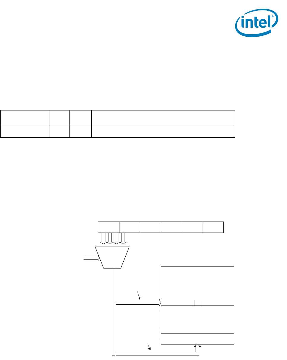
Multicast Table Array - MTA (05200h + 4*n [n..127]; R/W) — Intel® 82575EB Gigabit Ethernet
Controller
324632-003 Intel® 82575EB Gigabit Ethernet Controller
Revision: 2.1 Software Developer’s Manual and EEPROM Guide
January 2011 379
14.5.1 Multicast Table Array - MTA (05200h + 4*n
[n..127]; R/W)
There is one register per 32 bits of the Multicast Address Table for a total of 128 registers (the
MTA[127:0] designation). Software must mask to the desired bit on reads and supply a 32-bit word on
writes. The first bit of the address used to access the table is set according to the RX_CTRL.MO field.
Note: All accesses to this table must be 32 bit.
Figure 33 shows the multicast lookup algorithm. The destination address shown represents the
internally stored ordering of the received DA. Note that bit 0 indicated in this diagram is the first on the
wire.
Figure 33. Multicast Table Array
Field Bit(s) Initial
Value Description
Bit Vector 31:0 X Word wide bit vector specifying 32 bits in the multicast address
filter table.
47:40 39:32 31:24 23:16 15:8 7:0
pointer[11:5]
Multicast Table Arra
y
32 x 128
(4096 bit vector)
...
...
pointer[4:0]
word
bit
?
Destination Address
RCTL.MO[1:0]

Intel® 82575EB Gigabit Ethernet Controller — Receive Address Low - RAL (05400h + 8*n
[n=0..15]; R/W)
Intel® 82575EB Gigabit Ethernet Controller 324632-003
Software Developer’s Manual and EEPROM Guide Revision: 2.1
380 January 2011
14.5.2 Receive Address Low - RAL (05400h + 8*n
[n=0..15]; R/W)
Note: "n" is the exact unicast/multicast address entry and it is equals to 0,1,…15.
These registers contain the lower bits of the 48 bit Ethernet address. All 32 bits are valid.
These registers are reset by a software reset or platform reset. If an EEPROM is present, the first
register (RAL0) is loaded from the EEPROM after a software or platform reset.
Note: The RAL field should be written in network order.
14.5.3 Receive Address High - RAH (05404h + 8n
[n=0..15]; R/W)
"n" is the exact unicast/multicast address entry and it is equals to 0,1,…15.
These registers contain the upper bits of the 48 bit Ethernet address. The complete address is [RAH,
RAL]. AV determines whether this address is compared against the incoming packet and is cleared by a
master reset.
ASEL enables the 82575 to perform special filtering on receive packets.
After reset, if an EEPROM is present, the first register (Receive Address Register 0) is loaded from the
IA field in the EEPROM with its Address Select field set to 00b and its Address Valid field set to 1b. If no
EEPROM is present, the Address Valid field is set to 0b and the Address Valid field for all of the other
registers is set to 0b.
Note: The RAH field should be written in network order.
The first receive address register (RAH0) is also used for exact match pause frame checking (DA
matches the first register). As a result, RAH0 should always be used to store the individual Ethernet
MAC address of the 82575.
Field Bit(s) Initial
Value Description
RAL 31:0 X Receive address low
Contains the lower 32-bit of the 48-bit Ethernet address.

VLAN Filter Table Array - VFTA (05600h + 4*n [n=0..127]; R/W) — Intel® 82575EB Gigabit
Ethernet Controller
324632-003 Intel® 82575EB Gigabit Ethernet Controller
Revision: 2.1 Software Developer’s Manual and EEPROM Guide
January 2011 381
14.5.4 VLAN Filter Table Array - VFTA (05600h + 4*n
[n=0..127]; R/W)
There is one register per 32 bits of the VLAN Filter Table. The size of the word array depends on the
number of bits implemented in the VLAN Filter Table. Software must mask to the desired bit on reads
and supply a 32-bit word on writes.
Note: All accesses to this table must be 32 bit.
The algorithm for VLAN filtering using the VFTA is identical to that used for the Multicast Table Array.
Refer to Section 14.5.1 for a block diagram of the algorithm. If VLANs are not used, there is no need to
initialize the VFTA.
Field Bit(s) Initial
Value Description
RAH 15:0 X Receive address High
Contains the upper 16 bits of the 48-bit Ethernet address.
ASEL 17:16 X Address Select
Selects how the address is to be used in the address filtering.
00b = Destination address (required for normal mode)
01b = Source address
10b = Reserved
11b = Reserved
QSEL 19:18 00b Queue Select
Association through MAC address - selects one of the four receive queues for
packets matching this destination address.
00b = Queue 0
01b = Queue 1
10b = Queue 2
11b = Queue 3
Association through MAC address + RSS - serves as a pool bit, identifying the
target pool:
QSEL[19] = 0b - pool 0
QSEL[19] = 1b - pool 1
Reserved 30:20 0b Reserved
Reads as 0b.
Ignored on writes.
AV 31 Address Valid
Cleared after master reset. If an EEPROM is present, the Address Valid field of
the Receive Address Register 0 is set to 1b after a software or PCI reset or
EEPROM read.
In entries 0-15 this bit is cleared by master reset.
Field Bit(s) Initial
Value Description
Bit Vector 31:0 X Double-word wide bit vector specifying 32 bits in the VLAN Filter table.

Intel® 82575EB Gigabit Ethernet Controller — Multiple Receive Queues Command Register - MRQC
(05818h; R/W)
Intel® 82575EB Gigabit Ethernet Controller 324632-003
Software Developer’s Manual and EEPROM Guide Revision: 2.1
382 January 2011
14.5.5 Multiple Receive Queues Command Register -
MRQC (05818h; R/W)
Notes:
1. MRQC_EN is used for enable/disable RSS hashing and also for enabling multiple receive queues. Disabling this feature is not
recommended. Model usage is to reset the 82575 after disabling the RSS.
2. Packet would be tagged as IPv6 if it is without any of the Home-Address-Option field and Routing-Header-Type-2 field. As a
result, if a packet is tagged with IPv6 (type 5) in this case, the device driver would have to convert it to IPv6Ex (type 4).
Field Bit(s) Initial
Value Description
MRQE 2:0 00h Multiple Receive Queues Enable
Enables support for Multiple Receive Queues and defines the mechanism that controls
queue allocation. Note that the RXCSUM.PCSD bit must also be set to enable Multiple
Receive Queues.
000b = Multiple Receive Queues are disabled.
001b = Reserved.
010b = Multiple receive queues as defined by RSS for four queues.
011b = Multiple receive queues as defined by VMDq based on packet destination MAC
address.
100b = Multiple receive queues as defined by VMDq based on packet VLAN tag ID.
101b = Multiple receive queues as defined by VMDq based on packet destination MAC
address and RSS.
110b = Multiple receive queues as defined by VMDq based on packet VLAN tag ID and
RSS.
111b = Reserved.
In SKUs not supporting VT, The only functional values for this field are 000b and 010b.
Writing any other value is treated as if a value of zero was written. A value other than
zero might cause unexpected results.
Note: When RSS is enabled (MRQC.MRQE equals 010b, 101b or 110b), TCP Rx
checksum must also be enabled (RXCSUM.TUOFL = 1b).
RSS Interrupt
Enable
2 0h RSS Interrupt Enable
When set, this bit enables interrupt control by the RSS Interrupt Mask register. When
cleared, a receive packet generates an interrupt indication independent of the RSS
Interrupt registers.
Reserved 15:3 0h Reserved.
RSS Field
Enable
31:16 0h Each bit, when set, enables a specific field selection to be used by the hash function.
Several bits can be set at the same time.
Bit[16] = Enable TcpIPv4 hash function
Bit[17] = Enable IPv4 hash function
Bit[18] = Enable TcpIPv6Ex hash function
Bit[19] = Enable IPv6Ex hash function
Bit[20] = Enable IPv6 hash function
Bit[21] = Enable TCPIPv6 has function
Bit[22] = Enable UDPIPv4
Bit[23] = Enable UDPIPv6
Bit[24] = Enable UDPIPv6Ext
Bits[31:25] = Reserved; set to 0b.
Redirection Table - RETA (05C00h + 4*n [n=0..31]; R/W) — Intel® 82575EB Gigabit Ethernet
Controller
324632-003 Intel® 82575EB Gigabit Ethernet Controller
Revision: 2.1 Software Developer’s Manual and EEPROM Guide
January 2011 383
14.5.6 Redirection Table - RETA (05C00h + 4*n
[n=0..31]; R/W)
The redirection table is a 128-entry table with each entry being eight bits wide. Only seven bits of each
entry are used to store the tag value (five bits for the CPU index and two bits for queue index). The
table is configured through the following R/W registers.
. . .
Each entry (byte) of the indirection table contains the following information.
• Bits 7:6 - Queue index pool 1 or regular RSS.
• Bits 5:4 - Reserved
• Bits 3:2 - Queue index pool 0 (relevant only if MRQC.MRQE = 101b or 110b)
• Bits 1:0 - Reserved
The contents of the indirection table are not defined following reset of the Memory Configuration
registers. System software must initialize the table prior to enabling multiple receive queues. It might
also update the indirection table during run time. Such updates of the table are not synchronized with
the arrival time of received packets. Therefore, it is not guaranteed that a table update takes effect on
a specific packet boundary.
Note: If the operating system provides an indirection table whose size is smaller than 128 bytes,
software usually replicates the operating system-provided indirection table to span the
whole 128 bytes of the hardware's indirection table
DW 31 24 23 16 15 8 7 0
0 Tag 3 Tag 2 Tag 1 Tag 0
1 . . . . . .
DW 31 24 23 16 15 8 7 0
30
31 Tag 127 ... ... ...
Field Bit(s) Initial
Value Description
Entry 0 7:0 X Determines the tag value and physical queue for index 4*n + 0 (n=0..31).
Entry 1 15:8 X Determines the tag value and physical queue for index 4*n + 1 (n=0..31).
Entry 2 23:16 X Determines the tag value and physical queue for index 4*n + 2 (n=0..31).
Entry 3 31:24 X Determines the tag value and physical queue for index 4*n + 3 (n=0..31).
7:6 5:4 3:2 1:0
Queue index pool 1
(default)
Reserved Queue index pool 0 Reserved
Intel® 82575EB Gigabit Ethernet Controller — RSS Random Key Register - RSSRK (05C80h + 4*n
[n=0..9]; R/W)
Intel® 82575EB Gigabit Ethernet Controller 324632-003
Software Developer’s Manual and EEPROM Guide Revision: 2.1
384 January 2011
14.5.7 RSS Random Key Register - RSSRK (05C80h +
4*n [n=0..9]; R/W)
The RSS Random Key register stores a 40 byte key used by the RSS hash function.
. . .
14.5.8 VMDq Control - VMD_CTRL (0581Ch; R/W)
DW 31 24 23 16 15 8 7 0
0 K[3] K[2] K[1] K[0]
1 . . .
DW 31 24 23 16 15 8 7 0
6
7 K[39} ... ... K[36]
Field Bit(s) Initial Value Description
K0 7:0 00h Byte n*4 of the RSS random key (n=0,1,…9).
K1 15:8 00h Byte n*4+1 of the RSS random key (n=0,1,…9).
K2 23:16 00h Byte n*4+2 of the RSS random key (n=0,1,…9).
K3 31:24 00h Byte n*4+3 of the RSS random key (n=0,1,…9).
Field Bit(s) Initial
Value Description
Default VMDq
Queue #0
1:0 00b Determines the target queue for received packets that cannot be classified by the
VMDq procedures (for example, broadcast packets) or packets allocated to pool 0
that cannot be decoded by RSS. Operates differently in each mode:
Association through MAC address - defines default queue number.
Association through MAC address + RSS - Defines the default queue for packets
allocated to pool 0.
Reserved 6:2 0h Reserved
Default VMDq
Queue #1
8:7 00b Determines the target queue for received packets that cannot be classified by the
VMDq procedures (for example, broadcast packets) or packets allocated to pool 1
that cannot be decoded by RSS. Operates differently in each mode:
Association through MAC address - reserved.
Association through MAC address + RSS - defines the default queue for packets
allocated to pool 1.
Reserved 30:9 0h Reserved
Default Pool 31 0b Determines the target pool for received packets that cannot be classified by the
VMDq procedures (for example, broadcast packets). Operates differently in each
mode:
Association through MAC address - reserved
Association through MAC address + RSS - defines the default pool for packets that
cannot be allocated to any pool.

VLAN Filter Queue Array 0 - VFQA0 (0B100h + 4*n [n=0…127]; R/W) — Intel® 82575EB Gigabit
Ethernet Controller
324632-003 Intel® 82575EB Gigabit Ethernet Controller
Revision: 2.1 Software Developer’s Manual and EEPROM Guide
January 2011 385
14.5.9 VLAN Filter Queue Array 0 - VFQA0 (0B100h +
4*n [n=0…127]; R/W)
This register set classifies receive packets into Rx queues in some schemes for multiple queues. There
is one register per 32 bits of the VLAN Filter Queue Array 0. The VLAN Filter Queue Array 0, together
with the VLAN Filter Queue Array 1, determines the receive queue for received VLAN packets.
• All accesses to this table must be 32 bit.
14.5.10 VLAN Filter Queue Array 1 - VFQA1 (0B200h +
4*n [n=0…127]; R/W)
This register set classifies receive packets into Rx queues in some schemes for multiple queues. There
is one register per 32 bits of the VLAN Filter Queue Array 1. The VLAN Filter Queue Array 1, together
with the VLAN Filter Queue Array 0, determines the receive queue for received VLAN packets. VLAN
Filter Queue Array 1 can alternatively serve as a pool bit in some of the classification schemes.
Note: All accesses to this table must be 32 bit.
14.6 Wakeup Registers
This section contains detailed descriptions for those registers associated with the 82575’s wakeup
capabilities.
14.6.1 Wakeup Control Register - WUC (05800h; R/W)
The PME_En and PME_Status bits of this register are reset when Internal_Power_On_Reset is 0b. When
AUX_PWR = 0b, this register is also reset by de-asserting PE_RST_N and when transitioning from D3 to
D0. The other bits are reset using the standard internal resets.
Field Bit(s) Initial
Value Description
Bit Vector 31:0 0h Double word wide bit vector specifying 32 bits in the VLAN filter queue
array 0.
Field Bit(s) Initial
Value Description
Bit Vector 31:0 0h Double word wide bit vector specifying 32 bits in the VLAN filter queue
array 1.

Intel® 82575EB Gigabit Ethernet Controller — Wakeup Filter Control Register - WUFC (05808h; R/
W)
Intel® 82575EB Gigabit Ethernet Controller 324632-003
Software Developer’s Manual and EEPROM Guide Revision: 2.1
386 January 2011
14.6.2 Wakeup Filter Control Register - WUFC
(05808h; R/W)
This register is used to enable each of the pre-defined and flexible filters for wakeup support. A value of
1b means the filter is turned on.; A value of 0b means the filter is turned off.
If the NoTCO bit is set, then any packet that passes the manageability packet filtering described in the
Total Cost of Ownership (TCO) System Management Bus Interface Application Note does not cause a
Wake Up event even if it passes one of the Wake Up Filters. This bit is set at initialization and during
any EEPROM read if the SMBus Enable bit of the EEPROM's Management Control word is 1b. Otherwise
its initial value is 0b.
Field Bit(s) Initial
Value Description
APME 0 0b1
1. Loaded from the EEPROM.
Advance Power Management Enable
If set to 1b, APM Wakeup is enabled.
If this bit is set and the APMPME bit is cleared, reception of a magic packet asserts
the WUS.MAG bit but does not assert a PME.
PME_En 1 0b PME_En
This read/write bit is used by the software device driver to access the PME_En bit of
the Power Management Control / Status Register (PMCSR) without writing to the
PCIe* configuration space.
PME_Status 2 0b PME_Status
This bit is set when the 82575 receives a wakeup event. It is the same as the
PME_Status bit in the Power Management Control / Status Register (PMCSR).
Writing a 1b to this bit clears the PME_Status bit in the PMCSR.
APMPME 3 0b1Assert PME On APM Wakeup
If set to 1b, the 82575 sets the PME_Status bit in the Power Management Control /
Status Register (PMCSR) and asserts PME# when APM Wakeup is enabled and the
82575 receives a matching Magic Packet.
Reserved 31:4 0h Reserved
Field Bit(s) Initial Value Description
LNKC 0 0b Link Status Change Wakeup Enable.
MAG 1 0b Magic Packet Wakeup Enable.
EX 2 0b Directed Exact Wakeup Enable.
MC 3 0b Directed Multicast Wakeup Enable.
BC 4 0b Broadcast Wakeup Enable.
ARP 5 0b ARP Request Packet Wakeup Enable.
IPv4 6 0b Directed IPv4 Packet Wakeup Enable.
IPv6 7 0b Directed IPv6 Packet Wakeup Enable.
Reserved 14:8 0b Reserved. Set these bits to 0b.
NoTCO 15 0 Ignore TCO/management packets for wakeup.
FLX0 16 0b Flexible Filter 0 Enable.
FLX1 17 0b Flexible Filter 1 Enable.
Wakeup Status Register - WUS (05810h; R/W1C) — Intel® 82575EB Gigabit Ethernet Controller
324632-003 Intel® 82575EB Gigabit Ethernet Controller
Revision: 2.1 Software Developer’s Manual and EEPROM Guide
January 2011 387
14.6.3 Wakeup Status Register - WUS (05810h; R/
W1C)
This register is used to record statistics about all wakeup packets received. If a packet matches multiple
criteria then multiple bits could be set. Writing a 1b to any bit clears that bit.
This register is not cleared when RST# is asserted. It is only cleared when Internal_Power_On_Reset is
de-asserted or when cleared by the software device driver.
Note: If additional packets are received that matches one of the wakeup filters, after the original
wakeup packet is received, the WUS register is updated with the matching filters
accordingly.
14.6.4 IP Address Valid - IPAV (5838h; R/W)
The IP Address Valid indicates whether the IP addresses in the IP Address Table are valid.
FLX2 18 0b Flexible Filter 2 Enable.
FLX3 19 0b Flexible Filter 3 Enable.
Reserved 31:20 0h Reserved.
Field Bit(s) Initial Value Description
LNKC 0 0b Link Status Change.
MAG 1 0b Magic Packet Received.
EX 2 0b Directed Exact Packet Received
The packet’s address matched one of the 16 pre-programmed exact values in the
Receive Address registers.
MC 3 0b Directed Multicast Packet Received
The packet was a multicast packet hashed to a value that corresponded to a 1 bit in
the Multicast Table Array.
BC 4 0b Broadcast Packet Received.
ARP 5 0b ARP Request Packet Received.
IPv4 6 0b Directed IPv4 Packet Received.
IPv6 7 0b Directed IPv6 Packet Received.
MNG 8 0b Indicates that a manageability event that should cause a PME happened.
Reserved 15:9 0b Reserved.
FLX0 16 0b Flexible Filter 0 Match.
FLX1 17 0b Flexible Filter 1 Match.
FLX2 18 0b Flexible Filter 2 Match.
FLX3 19 0b Flexible Filter 3 Match.
Reserved 31:20 0b Reserved.
Field Bit(s) Initial Value Description
V40 0 0b IPv4 Address 0 Valid.
V41 1 0b IPv4 Address 1 Valid.
Field Bit(s) Initial Value Description
Intel® 82575EB Gigabit Ethernet Controller — IPv4 Address Table - IP4AT (05840h + 8*n
[n=0..3]; R/W)
Intel® 82575EB Gigabit Ethernet Controller 324632-003
Software Developer’s Manual and EEPROM Guide Revision: 2.1
388 January 2011
14.6.5 IPv4 Address Table - IP4AT (05840h + 8*n
[n=0..3]; R/W)
The IPv4 Address Table is used to store the four IPv4 addresses for the ARP/IPv4 Request packet and
Directed IP packet wakeup.
Note: This table is not cleared by any reset.
14.6.6 IPv6 Address Table - IP6AT (05880h +
4*n[n=0..3]; R/W)
The IPv6 Address Table is used to store the IPv6 addresses for Neighbor Discovery packet filtering and
Directed IP packet wakeup.
Note: This table is not cleared by any reset.
V42 2 0b IPv4 Address 2 Valid.
V43 3 0b IPv4 Address 3 Valid.
Reserved 15:4 0h Reserved.
V60 16 0b IPv6 Address 0 Valid.
Reserved 31:17 0b Reserved.
DWORD# Address 31 0
0 5840h IPV4ADDR0
2 5848h IPV4ADDR1
3 5850h IPV4ADDR2
4 5858h IPV4ADDR3
Field Dword # Address Bit(s) Initial Value Description
IPV4ADDR0 0 5840h 31:0 X IPv4 Address 0
IPV4ADDR1 2 5848h 31:0 X IPv4 Address 1
IPV4ADDR2 4 5850h 31:0 X IPv4 Address 2
IPV4ADDR3 6 5858h 31:0 X IPv4 Address 3
DWORD# Address 31 0
0 5880h IPV6ADDR0
1 5884h
2 5888h
3 588Ch
Wakeup Packet Length - WUPL (05900h; RC) — Intel® 82575EB Gigabit Ethernet Controller
324632-003 Intel® 82575EB Gigabit Ethernet Controller
Revision: 2.1 Software Developer’s Manual and EEPROM Guide
January 2011 389
14.6.7 Wakeup Packet Length - WUPL (05900h; RC)
This register indicates the length of the first wakeup packet received. It is valid if one of the bits in the
Wakeup Status register (WUS) is set. It is not cleared by any reset.
14.6.8 Wakeup Packet Memory (128 Bytes) - WUPM
(05A00h + 4*n [n=0..31]; RC)
This register is read-only and it is used to store the first 128 bytes of the wakeup packet for software
retrieval after system wakeup. It is not cleared by any reset.
14.6.9 Flexible Filter Mask Table - FFMT (09000h + 8*n
[n=0..127]; R/W)
The Flexible Filter Mask and Table is used to store the four 1-bit masks for each of the first 128 data
bytes in a packet, one for each Flexible Filter. If the mask bit is set to 1b, the corresponding Flexible
Filter compares the incoming data byte at the index of the mask bit to the data byte stored in the
Flexible Filter Value Table.
Before writing to the Flexible Filter Mask Table the driver must first disable the flexible filters by writing
0b’s to the Flexible Filter Enable bits of the Wakeup Filter Control Register (WUFC.FLXn).
Field Dword # Address Bit(s) Initial Value Description
IPV6ADDR0 0 5880h 31:0 X IPv6 Address 0, bytes 1-4
1 5884h 31:0 X IPv6 Address 0, bytes 5-8
2 5888h 31:0 X IPv6 Address 0, bytes 9-12
3 588Ch 31:0 X IPv6 Address 0, bytes 16-13
Field Bit(s) Initial Value Description
LEN 11:0 X Length of wakeup packet. (If jumbo frames is enabled and the packet is longer than
2047 bytes then this field is 2047.)
Reserved 31:12 0h Reserved
Field Bit(s) Initial
Value Description
WUPD 31:0 X Wakeup Packet Data
31 0 31 4 3 0
Reserved Reserved Byte 0 Mask
Reserved Reserved Byte 1 Mask
Reserved Reserved Byte 2 Mask
Reserved Reserved Byte 126 Mask
Reserved Reserved Byte 127 Mask
Intel® 82575EB Gigabit Ethernet Controller — Flexible Filter Value Table - FFVT (09800h + 8*n
[n=0..127]; R/W)
Intel® 82575EB Gigabit Ethernet Controller 324632-003
Software Developer’s Manual and EEPROM Guide Revision: 2.1
390 January 2011
14.6.10 Flexible Filter Value Table - FFVT (09800h + 8*n
[n=0..127]; R/W)
The Flexible Filter Value and Table is used to store the one value for each byte location in a packet for
each flexible filter. If the corresponding mask bit is set to 1b, the Flexible Filter compares the incoming
data byte to the values stored in this table.
Before writing to the Flexible Filter Value Table the driver must first disable the flexible filters by writing
0b’s to the Flexible Filter Enable bits of the Wakeup Filter Control Register (WUFC.FLXn).
14.6.11 Flexible Filter Length Table - FFLT (05F00h +
8*n [n=0..3]; R/W)
The flexible filter length table stores the minimum packet lengths required to pass each of the flexible
filters. Any packets that are shorter than the programmed length do not pass that filter. Each flexible
filter considers a packet that doesn't have any mismatches up to that point to have passed the flexible
filter when it reaches the required length. It does not check any bytes past that point.
Field Dword
#Address Bit(s) Initial Value Description
MASK0 0 9000h 7:0 X Mask for Filter [3:0] for Byte 0
MASK1 2 9008h 7:0 X Mask for Filter [3:0] for Byte 2
MASK2 4 9010h 7:0 X Mask for Filter [3:0] for Byte 3
...
MASK12
7
254 93F8h 7:0 X Mask for Filter [3:0] for Byte 127
31 0 31 24 23 16 15 8 7 0
Reserved Byte0: Value3 Value2 Value1 Value0
Reserved Byte1: Value3 Value2 Value1 Value0
Reserved Byte2: Value3 Value2 Value1 Value0
Reserved Byte127: Value3 Value2 Value1 Value0
Field Dword
#Address Bit(s) Initial Value Description
MASK0 0 9800h 15:0 X Mask for Filter [3:0] for Byte 0
MASK1 2 9808h 15:0 X Mask for Filter [3:0] for Byte 2
MASK2 4 9810h 15:0 X Mask for Filter [3:0] for Byte 3
...
MASK12
7
254 9BF8h 15:0 X Mask for Filter [3:0] for Byte 127
Manageability Registers — Intel® 82575EB Gigabit Ethernet Controller
324632-003 Intel® 82575EB Gigabit Ethernet Controller
Revision: 2.1 Software Developer’s Manual and EEPROM Guide
January 2011 391
All reserved fields read as 0's and ignore writes.
Note: Before writing to the flexible filter length table the software device driver must first disable
the flexible filters by writing 0's to the Flexible Filter Enable bits of the Wake Up Filter
Control (WUFC.FLXn) register.
Flexible filter cannot operate with a 1-byte pattern. Filters operate properly with all other
allowed pattern length (2-7FFh).
14.7 Manageability Registers
All management registers are controlled by the BMC for both read and write. Host accesses to the
management registers are blocked (read and write) unless debug write is enabled. The attributes for
the fields in this section refer to the BMC access rights.
14.7.1 Management VLAN TAG Value - MAVTV (5010h
+4*n [n=0..7]; R/W)
Where “n” is the VLAN filter serial number, equal to 0,1,…7.
The MAVTV registers are written by the BMC and are not accessible to the host for writing. The registers
are used to filter manageability packets as described in the Intel® 82575 GbE Controller System
Manageability Interface Application Note.
31 0 31 11 10 0
Reserved Reserved Reserved Length 0
Reserved Reserved Length 1
Reserved Reserved Length 2
Reserved Reserved Length 3
Field Bits Initial
Value Description
LEN 10:0 0b Minimum length for flexible filter i (i=0..3)
Reserved 11:31 0b Reserved
Field Bits Initial
Value Description
VID 11:0 00h Contains the VLAN ID that should be compared with the incoming
packet if the corresponding bit in MFVAL.VLAN is set.
Rsv 31:12 00h Reserved.

Intel® 82575EB Gigabit Ethernet Controller — Management Flex UDP/TCP Ports - MFUTP (5030h
+ 4*n [n=0..7]; R/W)
Intel® 82575EB Gigabit Ethernet Controller 324632-003
Software Developer’s Manual and EEPROM Guide Revision: 2.1
392 January 2011
14.7.2 Management Flex UDP/TCP Ports - MFUTP
(5030h + 4*n [n=0..7]; R/W)
Where each 32-bit register (n=0,…,7) refers to two port filters (register 0 refers to ports 0 and 1,
register 2 refers to ports 2 and 3, etc.).
The MFUTP registers are written by the BMC and not accessible to the host for writing. The registers are
used to filter manageability packets as described the Intel® 82575 GbE Controller System
Manageability Interface Application Note.
Reset - The MFUTP registers are cleared on Internal_Power_On_Reset only. The initial values for this
register can be loaded from the EEPROM after a power-on reset.
Note: The MFUTP_even and MFUTP_odd fields should be written in network order.
14.7.3 Management Control Register - MANC (05820h;
R/W)
The MANC register is written by the BMC and is not accessible to the host for writing.
Field Bits Initial
Value Description
MFUTP_even 15:0 0b i Management flex UDP/TCP port.
MFUTP_odd 31:16 0b i + 1 Management flex UDP/TCP port.
Field Bits Initial
Value Description
Reserved 15:0 0b Reserved.
TCO_RESET 16 0b TCO Reset Occurred
Set to 1b on a TCO reset.
This bit is only reset by an Internal_Power_On_Reset.
RCV_TCO_EN 17 0b Receive TCO Packets Enabled
When this bit is set, it enables the receive flow from the wire to the
manageability block.
KEEP_PHY_LINK_UP 18 0b Block PHY Reset and Power State Changes
When this bit is set, the PHY reset and power state changes do not get to the
PHY. This bit cannot be written unless the Keep_PHY_Link_Up_En EEPROM bit is
set.
This bit is reset after an Internal_Power_On_Reset.
RCV_ALL 19 0b Receive All Enable
When set, all received packets that passed L2 filtering are directed to the
manageability block.
MCST_PASS_L2 20 0b Receive All Multicast
When set, all received multicast packets pass L2 filtering and can be directed to
the manageability block by one of the decision filters. Broadcast packets are not
forwarded by this bit.
EN_MNG2HOST 21 0b Enable MNG Packets to Host Memory
This bit enables the functionality of the MANC2H register. When set, the packets
that are specified in the MANC2H register are also sent to host memory as long
as they pass the manageability filters.

Manageability Filters Valid - MFVAL (5824h; R/W) — Intel® 82575EB Gigabit Ethernet Controller
324632-003 Intel® 82575EB Gigabit Ethernet Controller
Revision: 2.1 Software Developer’s Manual and EEPROM Guide
January 2011 393
14.7.4 Manageability Filters Valid - MFVAL (5824h; R/
W)
The manageability filters valid registers indicate which filter registers contain a valid entry.
Reset - The MFVAL register is cleared on an Internal_Power_On_Reset and firmware reset.
The initial values for this register can be loaded from the EEPROM after an Internal_Power_On_Reset or
firmware reset. The MFVAL register is written by the BMC and is not accessible to the host for writing.
Reserved 22 0b Reserved.
EN_XSUM_FILTER 23 0b Enable Xsum Filtering to Manageability
When set, only packets that pass L3 and L4 checksums are send to the
manageability block.
Hardware does not calculate the checksum of packets whose L2 + L3 header is
bigger than 256 bytes. The BMC should take care of the checksum check of such
packets.
EN_IPv4_FILTER 24 0b Enable IPv4 address Filters
When set, the last 128 bits of the MIPAF register are used to store four IPv4
addresses for IPv4 filtering. When cleared, these bits store a single IPv6 filter.
FIXED_NET_TYPE 25 0b Fixed Next Type
If set, only packets matching the net type defined by the NET_TYPE field pass to
manageability. Otherwise, both tagged and un-tagged packet can be forwarded
to manageability engine.
NET_TYPE 26 0b Net Type
0b = Pass only un-tagged packets.
1b = Pass only VLAN tagged packets.
Valid only if FIXED_NET_TYPE is set.
Reserved 31:27 00h Reserved.
Field Bits Initial
Value Description
MAC 3:0 00h1
1. Loaded from the EEPROM.
MAC
Indicates that if the MAC unicast filter registers (MMAH, MMAL) contain valid MAC
addresses. Bit 0 corresponds to filter 0, etc.
Reserved 7:4 00h1Reserved.
VLAN 15:8 00h1VLAN
Indicates that if the VLAN filter registers (MAVTV) contain valid VLAN tags. Bit 8
corresponds to filter 0, etc.
IPv4 19:16 00h1IPv4
Indicates that if the IPv4 address filters (MIPAF) contain valid IPv4 addresses. Bit 16
corresponds to IPv4 address 0. These bits apply only when IPv4 address filters are
enabled (MANC.EN_IPv4_FILTER=1b)
Reserved 23:20 00h1Reserved.
IPv6 27:24 00h1IPv6
Indicates that if the IPv6 address filter registers (MIPAF) contain valid IPv6 addresses. Bit
24 corresponds to address 0, etc. Bit 27 (filter 3) applies only when the IPv4 address
filters are not enabled (MANC.EN_IPv4_FILTER=0b).
Reserved 31:28 00h1Reserved.

Intel® 82575EB Gigabit Ethernet Controller — Management Control to Host Register - MANC2H
(5860h; R/W)
Intel® 82575EB Gigabit Ethernet Controller 324632-003
Software Developer’s Manual and EEPROM Guide Revision: 2.1
394 January 2011
14.7.5 Management Control to Host Register - MANC2H
(5860h; R/W)
The MANC2H register enables the routing of manageability packets to the host based on the decision
filter that routed it to the manageability micro-controller. Each manageability decision filter (MDEF) has
a corresponding bit in the MANC2H register. When a manageability decision filter (MDEF) routes a
packet to manageability, it also routes the packet to the host if the corresponding MANC2HOST bit is set
and if the EN_MNG2HOST bit is set. The EN_MNG2HOST bit serves as a global enable for the MANC2H
bits.
Reset - The MANC2H register is cleared on an Internal_Power_On_Reset and a firmware reset. The
initial values for this register can be loaded from the EEPROM after an Internal Power On Rest or
firmware reset.
14.7.6 Manageability Decision Filters- MDEF (5890h +
4*n [n=0..7]; R/W)
Where “n” is the decision filter.
Field Bits Initial
Value Description
Host Enable 7:0 00h1
1. Loaded from the EEPROM.
Host Enable
When set, indicates that packets routed by the manageability filters to the
manageability system are also sent to the host. Bit 0 corresponds to decision rule
0, etc.
Reserved 31:8 00h1Reserved
Field Bits Initial
Value Description
Unicast AND 0 0b1Unicast
Controls the inclusion of unicast address filtering in the manageability filter decision (AND
section).
Broadcast
AND
10b
1Broadcast
Controls the inclusion of broadcast address filtering in the manageability filter decision
(AND section).
VLAN AND 2 0b1VLAN
Controls the inclusion of VLAN address filtering in the manageability filter decision (AND
section).
IP Address 3 0b1IP Address
Controls the inclusion of IP address filtering in the manageability filter decision (AND
section).
Unicast OR 4 0b1Unicast
Controls the inclusion of unicast address filtering in the manageability filter decision (OR
section).
Broadcast
OR
50b
1Broadcast
Controls the inclusion of broadcast address filtering in the manageability filter decision
(OR section).

Manageability IP Address Filter - MIPAF (0x58B0-0x58EC; RW) — Intel® 82575EB Gigabit
Ethernet Controller
324632-003 Intel® 82575EB Gigabit Ethernet Controller
Revision: 2.1 Software Developer’s Manual and EEPROM Guide
January 2011 395
14.7.7 Manageability IP Address Filter - MIPAF
(0x58B0-0x58EC; RW)
The Manageability IP Address Filter register stores IP addresses for manageability filtering. The MIPAF
register can be used in two configurations, depending on the value of the MANC. EN_IPv4_FILTER bit:
• EN_IPv4_FILTER = 0b: the last 128 bits of the register store a single IPv6 address (IPV6ADDR3)
• EN_IPv4_FILTER = 1b: the last 128 bits of the register store four IPv4 addresses (IPV4ADDR[3:0])
The initial values for these registers can be loaded from the EEPROM after power-up reset. The
registers are written by the BMC and not accessible to the host for writing.
Reset - The registers are cleared on Internal_Power_On_Reset only.
The MIPAF registers value should be configured to the register in host order.
EN_IPv4_FILTER = 0b:
Multicast
AND
60b
1Multicast
Controls the inclusion of Multicast address filtering in the manageability filter decision
(AND section). Broadcast packets are not included by this bit. The packet must pass some
L2 filtering to be included by this bit – either by the MANC.MCST_PASS_L2 or by some
dedicated MAC address.
ARP Request 7 0b1ARP Request
Controls the inclusion of ARP Request filtering in the manageability filter decision (OR
section).
ARP
Response
80b
1ARP Response
Controls the inclusion of ARP Response filtering in the manageability filter decision (OR
section).
Neighbor
Discovery
90b
1Neighbor Discovery
Controls the inclusion of Neighbor Discovery filtering in the manageability filter decision
(OR section). The neighbor types accepted by this filter are types 86h, 87h, 88h & 89h
Port 0x298 10 0b1Port 0x298
Controls the inclusion of Port 0x298 filtering in the manageability filter decision (OR
section).
Port 0x26F 11 0b1Port 0x26F
Controls the inclusion of Port 0x26F filtering in the manageability filter decision (OR
section).
Flex port 27:12 00h1Flex port
Controls the inclusion of Flex port filtering in the manageability filter decision (OR
section). Bit 12 corresponds to flex port 0, etc.
Flex TCO 31:28 00h1Flex TCO
Controls the inclusion of Flex TCO filtering in the manageability filter decision (OR
section). Bit 28 corresponds to Flex TCO filter 0, etc.
1. Loaded from the EEPROM.
DWORD# Address 31 0
0 58B0h IPV6ADDR0
1 58B4h
2 58B8h
3 58BCh

Intel® 82575EB Gigabit Ethernet Controller — Manageability IP Address Filter - MIPAF (0x58B0-
0x58EC; RW)
Intel® 82575EB Gigabit Ethernet Controller 324632-003
Software Developer’s Manual and EEPROM Guide Revision: 2.1
396 January 2011
EN_IPv4_FILTER = 1b:
4 58C0h IPV6ADDR1
5 58C4h
6 58C8h
7 58CCh
8 58D0h IPV6ADDR2
9 58D4h
10 58D8h
11 58DCh
12 58E0h IPV6ADDR3
13 58E4h
14 58E8h
15 58ECh
Field Dword # Address Bit(s) Initial Value Description
0 58B0h 31:0 X IPv6 Address 0, bytes 1-4 (least significant byte is
first on the wire)
IPV6ADDR0 1 58B4h 31:0 X IPv6 Address 0, bytes 5-8
2 58B8h 31:0 X IPv6 Address 0, bytes 9-12
3 58BCh 31:0 X IPv6 Address 0, bytes 16-13
0 58C0h 31:0 X IPv6 Address 1, bytes 1-4 (least significant byte is
first on the wire)
IPV6ADDR1 1 58C4h 31:0 X IPv6 Address 1, bytes 5-8
2 58C8h 31:0 X IPv6 Address 1, bytes 9-12
3 58CCh 31:0 X IPv6 Address 1, bytes 16-13
0 58D0h 31:0 X IPv6 Address 2, bytes 1-4 (least significant byte is
first on the wire)
IPV6ADDR2 1 58D4h 31:0 X IPv6 Address 2, bytes 5-8
2 58D8h 31:0 X IPv6 Address 2, bytes 9-12
3 58DCh 31:0 X IPv6 Address 2, bytes 16-13
3 0 58E0h 31:0 X IPv6 Address 3, bytes 1-4 (least significant byte is
first on the wire)
IPV6ADDR 1 58E4h 31:0 X IPv6 Address 3, bytes 5-8
2 58E8h 31:0 X IPv6 Address 3, bytes 9-12
3 58ECh 31:0 X IPv6 Address 3, bytes 16-13
DWORD# Address 31 0
0 58B0h
1 58B4h IPV6ADDR0
2 58B8h
3 58BCh
4 58C0h
5 58C4h IPV6ADDR1
6 58C8h

Manageability IP Address Filter - MIPAF (0x58B0-0x58EC; RW) — Intel® 82575EB Gigabit
Ethernet Controller
324632-003 Intel® 82575EB Gigabit Ethernet Controller
Revision: 2.1 Software Developer’s Manual and EEPROM Guide
January 2011 397
7 58CCh
8 58D0h
9 58D4h IPV6ADDR2
10 58D8h
11 58DCh
12 58E0h IPV4ADDR0
13 58E4h IPV4ADDR1
14 58E8h IPV4ADDR2
15 58ECh IPV4ADDR3
Field Dword # Address Bit(s) Initial Value Description
0 58B0h 31:0 X IPv6 Address 0, bytes 1-4 (least significant
byte is first on the wire)
IPV6ADDR0 1 58B4h 31:0 X IPv6 Address 0, bytes 5-8
2 58B8h 31:0 X IPv6 Address 0, bytes 9-12
3 58BCh 31:0 X IPv6 Address 0, bytes 16-13
0 58C0h 31:0 X IPv6 Address 1, bytes 1-4 (least significant
byte is first on the wire)
IPV6ADDR1 1 58C4h 31:0 X IPv6 Address 1, bytes 5-8
2 58C8h 31:0 X IPv6 Address 1, bytes 9-12
3 58CCh 31:0 X IPv6 Address 1, bytes 16-13
0 58D0h 31:0 X IPv6 Address 2, bytes 1-4 (least significant
byte is first on the wire)
IPV6ADDR2 1 58D4h 31:0 X IPv6 Address 2, bytes 5-8
2 58D8h 31:0 X IPv6 Address 2, bytes 9-12
3 58DCh 31:0 X IPv6 Address 2, bytes 16-13
IPV4ADDR0 0 58E0h 31:0 X IPv4 Address 0 (least significant byte is first
on the wire)
IPV4ADDR1 1 58E4h 31:0 X IPv4 Address 1 (least significant byte is first
on the wire)
IPV4ADDR2 2 58E8h 31:0 X IPv4 Address 2 (least significant byte is first
on the wire)
IPV4ADDR3 3 58ECh 31:0 X IPv4 Address 3 (least significant byte is first
on the wire)
Field Bit(s) Initial
Value Description
IP_ADDR 4 bytes 31:0 X Four bytes of IP (v6 or v4) address
i mod 4 = 0 bytes 1 – 4
i mod 4 = 1 bytes 5 – 8
i mod 4 = 0 bytes 9 – 12
i mod 4 = 0 bytes 13 – 16
where i div four is the index of IP address (0..3).
Intel® 82575EB Gigabit Ethernet Controller — Manageability MAC Address Low - MMAL (5910h +
8*n[n=0..3]; RW)
Intel® 82575EB Gigabit Ethernet Controller 324632-003
Software Developer’s Manual and EEPROM Guide Revision: 2.1
398 January 2011
14.7.8 Manageability MAC Address Low - MMAL (5910h
+ 8*n[n=0..3]; RW)
These registers contain the lower bits of the 48 bit Ethernet address. The MMAL registers are written by
the BMC and not accessible to the host for writing. The registers are used to filter manageability
packets.
Reset - The MMAL registers are cleared on Internal_Power_On_Reset only. The initial values for this
register can be loaded from the EEPROM by the management firmware after power-up reset.
The MMAL value should be configured to the register in host order.
14.7.9 Manageability MAC Address High - MMAH
(0x5914 + 8*n[n=0..3]; RW)
These registers contain the upper bits of the 48 bit Ethernet address. The complete address is {MMAH,
MMAL}. The MMAH registers are written by the BMC and not accessible to the host for writing. The
registers are used to filter manageability packets.
Reset - The MMAL registers are cleared on Internal_Power_On_Reset only. The initial values for this
register can be loaded from the EEPROM by the management firmware after power-up reset or
firmware reset.
The MMAH value should be configured to the register in host order.
14.7.10 Flexible TCO Filter Table Registers - FTFT
(09400h-097FCh; RW)
Each of the Four Flexible TCO Filters Table (FTFT) registers contains a 128-byte pattern and a
corresponding 128-bit mask array. If enabled, the first 128 bytes of the received packet are compared
against the non-masked bytes in the FTFT register.
Field Bit(s) Initial
Value Description
MMAL 31:0 X Manageability MAC Address Low
The lower 32 bits of the 48 bit Ethernet address.
Field Bit(s) Initial
Value Description
MMAH 15:0 X Manageability MAC Address High
The upper 16 bits of the 48 bit Ethernet address.
Reserved 31:16 00h Reserved
Reads as 00h. Ignored on writes.

Flexible TCO Filter Table Registers - FTFT (09400h-097FCh; RW) — Intel® 82575EB Gigabit
Ethernet Controller
324632-003 Intel® 82575EB Gigabit Ethernet Controller
Revision: 2.1 Software Developer’s Manual and EEPROM Guide
January 2011 399
Each 128-byte filter is composed of 32 Dword entries, where each two Dwords are accompanied by an
8-bit mask, one bit per filter byte. The bytes in each two Dwords are written in network order. For
example, byte0 written to bits [7:0], byte1 to bits [15:8] etc. The mask field is set so that bit0 in the
mask masks byte0, bit 1 masks byte 1 etc. A value of one in the mask field means that the appropriate
byte in the filter should be compared to the appropriate byte in the incoming packet.
Note: The mask field must be 8 bytes aligned even if the length field is not 8 bytes aligned as the
hardware implementation compares 8 bytes at a time so it should get extra masks until the
end of the next Qword. Any mask bit that is located after the length should be set to zero
indicating no comparison should be done.
In case the actual length, which is defined by the length field register and the mask bits, is
not 8 bytes aligned there might be a case that a packet which is shorter than the actual
required length pass the flexible filter. This can happen due to comparison of up to 7 bytes
that come after the packet but are not a real part of the packet.
The last Dword of each filter contains a length field defining the number of bytes from the beginning of
the packet compared by this filter. If actual packet length is less than the length specified by this field,
the filter fails. Otherwise, it depends on the result of actual byte comparison. The value should not be
greater than 128.
The initial values for the FTFT registers can be loaded from the EEPROM after power-up reset. The FTFT
registers are written by the BMC and not accessible to the host for writing. The registers are used to
filter manageability packets.
Reset - The FTFT registers are cleared on Internal_Power_On_Reset only.
…………..
31 8 31 8 7 0 31 0 31 0
Reserved Reserved Mask [7:0] Dword 1 Dword 0
Reserved Reserved Mask [15:8] Dword 3 Dword 2
Reserved Reserved Mask [23:16] Dword 5 Dword 4
Reserved Reserved Mask [31:24] Dword 7 Dword 6
31 8 31 8 7 0 31 0 31 0
Reserved Reserved Mask [127:120] Dword 29 Dword 28
Length Reserved Mask [127:120] Dword 31 Dword 30
Field Dword Address Bit(s) Initial Value
Filter 0 Dword0 0 09400h 31:0 X
Filter 0 Dword1 1 09404h 31:0 X
Filter 0 Mask[7:0] 2 09408h 7:0 X
Reserved 3 0940Ch X
Filter 0 Dword2 4 09410h 31:0 X
…
Filter 0 Dword30 60 094F0h 31:0 X
Filter 0 Dword31 61 094F4h 31:0 X
Filter 0 Mask[127:120] 62 094F8h 7:0 X
Length 63 094FCh 6:0 X

Intel® 82575EB Gigabit Ethernet Controller — Legacy Sensor Polling Mask 1...8 Register
(F8h:FFh)
Intel® 82575EB Gigabit Ethernet Controller 324632-003
Software Developer’s Manual and EEPROM Guide Revision: 2.1
400 January 2011
14.7.11 Legacy Sensor Polling Mask 1...8 Register
(F8h:FFh)
This register provides software an interface for the 8 legacy sensor polling data masks.
Each polling mask has the following format:
These registers are initialized to 0b after all EPROM reload events.
14.8 PCIe* Registers
14.8.1 PCIe* Control - GCR (05B00h; R)
Register Description
F8h Legacy Sensor Polling Mask #1.
F9h Legacy Sensor Polling Mask #2.
FAh Legacy Sensor Polling Mask #3.
FBh Legacy Sensor Polling Mask #4.
FCh Legacy Sensor Polling Mask #5.
FDh Legacy Sensor Polling Mask #6.
FEh Legacy Sensor Polling Mask #7.
FFh Legacy Sensor Polling Mask #8.
Bits Name Type Description / Function Default
7:0 POLL_MSK R/W Polling Mask for Polling Descriptor #N
This register is used to read and write the data mask
for Legacy Sensor Polling Descriptor #N.
0
Field Bit(s) Initial
Value Description
Reserved 31 0b Reserved
Self_Test_Result 30 0b If set, self test result finished successfully (after an Internal_Power_On_Reset).
GIO_Good_10s 29 0b Force good PCIe* L0s training (after an Internal_Power_On_Reset).
GIO_Dis_Rd_Err 28 0b Disable running disparity error of PCIe* 108b decoders (after an
Internal_Power_On_Reset).
L1_Act_Without_
L0s_Rx
27 0b If set, enables the 82575 to enter ASPM L1 active without any correlation of L0s_rx
(after an Internal_Power_On_Reset).
L1_Entry_Latency
(RO)
26:25 11b Determines the idle time of the PCIe* link in L0s state before initiating a transition
to L1 state. Initial value is loaded from the EEPROM.
00b - 64 s
01b - 256 s
10b - 1 ms
11b - 4 ms
PCIe* Control - GCR (05B00h; R) — Intel® 82575EB Gigabit Ethernet Controller
324632-003 Intel® 82575EB Gigabit Ethernet Controller
Revision: 2.1 Software Developer’s Manual and EEPROM Guide
January 2011 401
L0s_Entry_Lat 24 0b L0s Entry Latency
Set to 0b to indicate L0s entry latency is the same as L0s exit latency. Set to 1b to
indicate L0s entry latency is (L0s exit latency/4).
Reserved 23 0b Reserved
Reserved 22 1b Reserved
Must be set to 1b.
hdr_log Inversion 21 0b If set, the header log in error reporting is written as 31:0 to log1, 63:643 in log2. If
not set, the header is written as 127:96 in log1 95:64 in log 2 …..
PBA_CL_DEAS 20 0b If cleared, PBA is cleared on de-assertion of MSI-X request.
g_sa_250_2ph_en 19 0b Enables probed-data speed reduction to enable slow pads reflect 250 Mbaud signals
by splitting them into two phases, each 62.5 Mbaud. Effective only in GIO analog
standalone mode.
1b = enable (default).
0b = disabled.
PCIe* Capability
Version (RO)
18 0b Reports the PCIe* Capability Version Supported
0b = Capability version = 1h.
1b = Capability version = 2h.
Completion_
Timeout_Disable
(RO or RW1)
17 0b Indicates if PCIe* Completion Timeout is Supported (after an
Internal_Power_On_Reset)
0b = Completion timeout enabled.
1b = Completion timeout disabled.
Completion_
Timeout_Resend
16 1b When set, enables to resend a request once the completion timeout expired
0b = Do not resend request on completion timeout.
1b = Resend request on completion timeout.
This bit is used no matter which timeout mechanism is used.

Intel® 82575EB Gigabit Ethernet Controller — PCIe* Control - GCR (05B00h; R)
Intel® 82575EB Gigabit Ethernet Controller 324632-003
Software Developer’s Manual and EEPROM Guide Revision: 2.1
402 January 2011
Completion_
Timeout_Value
(RO or RW1)
15:12 0h Indicates the selected value for completion timeout (after an
Internal_Power_On_Reset).
Decoding of this field depends on the PCIe* capability version:
Capability version = 1 (bits 13:12):
00b = 50 s to 10 ms (default)
01b = 10 ms to 200 ms
10b = 200 ms to 4 s
11b = 4 s to 64 s
Bits 15:14 are reserved
Capability version = 2:
0000b = 50 s to 50 ms
0001b = 50 s to 100 s
0010b = 1 ms to 10 ms
0011b = Reserved
0100b = Reserved
0101b = 16 ms to 55 ms
0110b = 65 ms to 210 ms
0111b = Reserved
1000b = Reserved
1001b = 260 ms to 900 ms
1010b = 1 s to 3.5 s
1011b = Reserved
1100b = Reserved
1101b = 4 s to 13 s
1110b = 17 s to 64 s
1111b = Reserved
Reserved 11:10 00b Reserved
Rx_L0s_Adjustme
nt
9 1b If set, the replay timer always adds the required L0s adjustment (after an
Internal_Power_On_Reset).
When set to 0b, adds it only when Tx L0s are active (after an
Internal_Power_On_Reset).
FW
Self_Test_Enable
8 0b When set, firmware should perform a self test (after an Internal_Power_On_Reset).
Reserved 7:3 0h Reserved
CBDE (RO) 2 0b Data Movement Engine Transfer Enabled
Reflects the transfer enable bit received from the CB_RESPONSE message.
Field Bit(s) Initial
Value
Description
CBA (RO) 1 0b Data Movement Engine Active
This bit is set to 1b following reception of the response VDM sent by the data
movement engine.
If the I/OAT fuse is fused out, then this bit remains reset to 0b.
CBDB (WO) 0 0b Data Movement Engine Doorbell
This bit is used by the software device driver to trigger sending the data movement
engine.

Function Tag - FUNCTAG (05B08h; R/W) — Intel® 82575EB Gigabit Ethernet Controller
324632-003 Intel® 82575EB Gigabit Ethernet Controller
Revision: 2.1 Software Developer’s Manual and EEPROM Guide
January 2011 403
14.8.2 Function Tag - FUNCTAG (05B08h; R/W)
14.8.3 PCIe* Statistics Control #1 - GSCL_1 (05B10h;
R)
14.8.4 PCIe* Statistics Control #2 - GSCL_2 (05B14h;
R)
This counter contains the mapping of an event (which counter counts what event).
Field Bit(s) Initial
Value Description
cnt_0_tag 4:0 0h Tag number for event 6/1D, if located in counter 0.
cnt_0_func 7:5 0h Function number for event 6/1D, if located in counter 0.
cnt_1_tag 12:8 0h Tag number for event 6/1D, if located in counter 2.
cnt_1_func 15:13 0h Function number for event 6/1D, if located in counter 1.
cnt_2_tag 20:16 0h Tag number for event 6/1D, if located in counter 2.
cnt_2_func 23:21 0h Function number for event 6/1D, if located in counter 2.
cnt_3_tag 28:24 0h Tag number for event 6/1D, if located in counter 3.
cnt_3_func 31:29 0h Function number for event 6/1D, if located in counter 3.
Field Bit(s) Initial
Value Description
GIO_COUNT_
START
31 0b Start indication of PCIe* statistic counters.
GIO_COUNT_
STOP
30 0b Stop indication of PCIe* statistic counters.
GIO_COUNT_
RESET
29 0b Reset indication of PCIe* statistic counters.
GIO_64_BIT_
EN
28 0b Enable two 64-bit counters instead of four 32-bit counters.
GIO_COUNT_
TEST
27 0b Test Bit
Firmware counters for testability.
Reserved 26:4 0b Reserved.
GIO_COUNT_
EN_3
3 0b Enable PCIe* Statistic Counter Number 3.
GIO_COUNT_
EN_2
2 0b Enable PCIe* Statistic Counter Number 2.
GIO_COUNT_
EN_1
1 0b Enable PCIe* Statistic Counter Number 1.
GIO_COUNT_
EN_0
0 b0 Enable PCIe* Statistic Counter Number 0.

Intel® 82575EB Gigabit Ethernet Controller — PCIe* Statistics Control #2 - GSCL_2 (05B14h; R)
Intel® 82575EB Gigabit Ethernet Controller 324632-003
Software Developer’s Manual and EEPROM Guide Revision: 2.1
404 January 2011
Table 92 lists the encoding of the events.
Table 92. Event Encodings
Field Bit(s) Initial
Value Description
GIO_EVENT_
NUM_3
31:24 0b Event number that counter 3 counts.
GIO_EVENT_
NUM_2
23:16 0b Event number that counter 2 counts.
GIO_EVENT_
NUM_1
15:8 0b Event number that counter 1 counts.
GIO_EVENT_
NUM_0
7:0 0b Event number that counter 0 counts.
Transaction Layer Events Event
Mapping
(Hex) Description
Dwords of transaction layer packet
transmitted (transferred to the physical
layer), include payload and header.
0Each 125 MHz cycle, the counter increases by one (1 dw) or 2 (2
dw).
Counted: completion, memory, message (not replied)
All types of transmitted packets. 1Only TLP packets. Each cycle, the counter increases by one if TLP
packet was transmitted to the link.
Counted: completion, memory, message (not replied)
Transmit TLP Packets of function #0 2 Each cycle, the counter increases by one, if the packet was
transmitted.
Counted: memory, message of function 0 (not replied)
Transmit TLP Packets of function #1 3 Each cycle, the counter increases by one, if the packet was
transmitted
Counted: memory, message of function 1 (not replied)
Non posted Transmit TLP packets of
function #0
4Each cycle, the counter increases by one, if the packet was
transmitted
Counted: memory (np) of function 0 (not replied)
Non posted Transmit TLP packets of
function #1
5Each cycle, the counter increases by one, if the packet was
transmitted
Counted: memory (np) of function 1 (not replied)
Transmit TLP Packets of function X and tag
Y, according to FUNC_TAG register
6Each cycle, the counter increases by one, if the packet was
transmitted
Counted: memory, message for a given func# and tag# (not
replied)
All types of received packets (TLP only) 1A Each cycle, the counter increases by one, if the packet was
received
Counted: completion (only good), memory, I/O, config
Receive TLP Packets of function #0 1B Each cycle, the counter increases by one, if the packet was
transmitted.
Counted: good completions of func#0
Receive TLP Packets of function #1 1C Each cycle, the counter increases by one, if the packet was
transmitted
Counted: good completions of func#1
Receive Completion Packets 1D Each cycle, the counter increases by one, if the packet was
received.
Counted: good completions for a given func# and tag#

PCIe* Statistics Control #2 - GSCL_2 (05B14h; R) — Intel® 82575EB Gigabit Ethernet Controller
324632-003 Intel® 82575EB Gigabit Ethernet Controller
Revision: 2.1 Software Developer’s Manual and EEPROM Guide
January 2011 405
Clock counter 20 Counts GIO cycles.
Bad TLP from LL 21 Each cycle, the counter increases by one, if bad TLP is received
(bad crc, error reported by AL, misplaced special char, reset in
thI of received tlp).
Header dwords of Transaction layer packet
transmitted.
25 Only TLP, each 125 MHz cycle the counter increases by one (1 dw
of header) or 2 (2 dw of header).
Counted: completion, memory, message (not replied)
Header dwords of Transaction layer packet
received.
26 Only TLP, each 125 MHz cycle the counter increases by one (1 dw
of header) or 2 (2 dw of header).
Counted: completion, memory, message
Transaction layer stalls transmitting due to
lack of flow control credits of the next part.
27 The counter counts the number of times Transaction layer Stop
transmitting because of this (per packet).
Counted: completion, memory, message
Retransmitted packets. 28 The Counter increases for each retransmitted packet.
Counted: completion, memory, message
Stall due to retry buffer full 29 The counter counts the number of times Transaction layer stop
transmitting because Retry buffer is full (per packet).
Counted: completion, memory, message
Retry buffer is under threshold 2A Threshold specified by software, Retry buffer is under threshold
per packet.
Counted: completion, memory, message
PRH (posted request header) flow control
credits (of the next part) below threshold
2B Threshold specified by software.
The counter increases each time number of the specific flow
control credits is lower than threshold.
Counted: According to credit type
PRD (posted request data) flow control
credits (of the next part) below threshold
2C
NPRH (non posted request header) flow
control credits (of the next part) below
threshold
2D
CPLH (completion header) flow control
credits (of the next part) below threshold
2E
CPLD (completion data) flow control credits
(of the next part) below threshold
2F
PRH (posted request header) flow control
credits (of local part) get to 0.
30 Threshold specified by software.
The counter increases each time number of the specific flow
control credits is get the value 0 (The period that the credit is 0
not counted).
Counted: According to credit type
NPRH (non posted request header) flow
control credits (of local part) get to 0.
31
PRD (posted request data) flow control
credits (of local part) get to 0.
32
NPRD (non posted request data) flow
control credits (of local part) get to 0.
33
Dwords of Transaction layer packet
received, include payload and header.
34 Each 125 MHz cycle the counter increases by one (1 dw) or 2 (2
dw).
Counted: completion, memory, message, I/O, config
Messages packets received 35 Each 125 MHz cycle the counter increases by one
Counted: messages (only good)
Received packets to func_logic. 36 Each 125 MHz cycle the counter increases by one
Counted: memory, I/O, config (only good)

Intel® 82575EB Gigabit Ethernet Controller — PCIe* Statistics Control #2 - GSCL_2 (05B14h; R)
Intel® 82575EB Gigabit Ethernet Controller 324632-003
Software Developer’s Manual and EEPROM Guide Revision: 2.1
406 January 2011
Average latency of read request – from
initialization until end of completions.
Estimated latency is ~5 s.
40 + 41 The software will select the client need to be tested.
The statistic counter will count the number of read request of the
required client.
In addition, the accumulated time of all requests will be saved in
a time accumulator.
The average time for read request will be
[Accumulated time / Number of read requests]
(Event 41 is for the counter)
Average latency of read request RTT– from
initialization until the first completion is
arrived (Round Trip Time).
Estimated latency is 1uSec
42 + 43 The software will select the client need to be tested.
The statistic counter will count the number of read request of the
required client.
In addition, the accumulated time of all RTT will be saved in a
time accumulator.
The average time for read request will be
[Accumulated time / Number of read requests]
(Event 43 is for the counter)
Requests that reached Time Out. 44 Number of requests that reached Time Out.
Completion Latency above Threshold 45 + 46 The software will select the client need to be tested.
The software will program the required threshold (in GSCL_4 –
units of 96 ns).
One statistic counter will count the time from the beginning of
the request until end of completions.
The other counter will count the number of events.
If the time is above threshold – add 1 to the event counter.
(Event 46 is for the counter)
Completion Latency above Threshold – for
RTT
47 + 48 The software will select the client need to be tested.
The software will program the required threshold (in GSCL_4 –
units of 96 ns).
One statistic counter will count the time from the beginning of
the request until first completion arrival.
The other counter will count the number of events.
If the time is above threshold – add 1 to the event counter.
(Event 48 is for the counter)
Dwords of packet transmitted (transferred
to the physical layer), include payload and
header.
50 Include DLLP (Link layer packets) and TLP (transaction layer
packets transmitted.
Each 125 MHz cycle the counter increase in 1 (1 dw) or 2 (2 dw).
Dwords of packet received (transferred to
the physical layer), include payload and
header.
51 Include DLLP (Link layer packets) and TLP (transaction layer
packets transmitted.
Each 125 MHz cycle the counter increase in 1 (1 dw) or 2 (2 dw).
All types of DLLP packets transmitted from
link layer.
52 Each cycle, the counter increases by one, if DLLP packet was
transmitted.
Flow control DLLP transmitted from link
layer.
53 Each cycle, the counter increases by one, if message was
transmitted
Ack DLLP transmitted. 54 Each cycle, the counter increases by one, if message was
transmitted.
All types of DLLP packets received. 55 Each cycle, the counter increases by one, if DLLP was received.

PCIe* Statistics Control #3 - GSCL_3 (05B18h; R/W) — Intel® 82575EB Gigabit Ethernet
Controller
324632-003 Intel® 82575EB Gigabit Ethernet Controller
Revision: 2.1 Software Developer’s Manual and EEPROM Guide
January 2011 407
14.8.5 PCIe* Statistics Control #3 - GSCL_3 (05B18h;
R/W)
This counter holds the threshold values needed for some of the event counting. The event increases
only after the value passes the threshold boundary.
14.8.6 PCIe* Statistics Control #4 - GSCL_4 (05B1Ch;
R/W)
This counter holds the threshold values needed for some of the event counting. The event increases
only after the value passes the threshold boundary.
14.8.7 PCIe* Counter #0 - GSCN_0 (05B20h; R/W)
14.8.8 PCIe* Counter #1 - GSCN_1 (05B24h; R/W)
Flow control DLLP received in Link layer. 56 Each cycle, the counter increases by one, if message was
received.
Ack DLLP received. 57 Each cycle, the increases by one, if message was received.
Nack DLLP received. 58 Each cycle, the counter increases by one, if message was
transmitted
Field Bit(s) Initial
Value Description
Reserved 31:28 0b Reserved.
GIO_FC_TH_1 27:16 0b Threshold of flow control credits.
Optional values: 0 - (256-1).
Reserved 15:12 0b Reserved.
GIO_FC_TH_0 11:0 0b Threshold of flow control credits.
Optional values: 0 - (256-1).
Field Bit(s) Initial
Value Description
Reserved 31:16 0b Reserved.
GIO_RB_TH 15:10 0b Retry buffer threshold.
GIO_COML_TH 9:0 0b Completions latency threshold.
31 0
Event Counter
31 0
Event Counter

Intel® 82575EB Gigabit Ethernet Controller — PCIe* Counter #2 - GSCN_2 (05B28h; R/W)
Intel® 82575EB Gigabit Ethernet Controller 324632-003
Software Developer’s Manual and EEPROM Guide Revision: 2.1
408 January 2011
14.8.9 PCIe* Counter #2 - GSCN_2 (05B28h; R/W)
14.8.10 PCIe* Counter #3 - GSCN_3 (05B2Ch; R/W)
14.8.11 Function Active and Power State to MNG -
FACTPS (05B30h; R)
Firmware uses this register for configuration.
31 0
Event Counter
31 0
Event Counter
Field Bit(s) Initial
Value Description
PM State
Changed
31 0b Indication that one or more of the functions power states had changed. This bit is also
a signal to the MNG unit to create an interrupt.
This bit is cleared on read, and is not set for at least 8 cycles after it was cleared.
LAN Function
Sel
30 0b When both LAN ports are enabled and the LAN Function Sel equals 0b, LAN 0 is routed
to PCIe* Function 0 and LAN 1 is routed to PCIe* Function 1. If the LAN Function Sel
equals 1b, LAN 0 is routed to PCIe* Function 1 and LAN 1 is routed to PCIe* Function 0.
If any of the LAN functions are disabled, the other one is routed to PCIe* Function 0
regardless of the LAN Function Sel. This bit is initiated by EEPROM word 21h.
MNGCG 29 0b MNG Clock Gated
When set, indicates that the manageability clock is gated.
Reserved 28:10 0h Reserved
Func1 Aux_En 9 0b Function 1 Auxiliary (AUX) Power PM Enable bit shadow from the configuration space.
LAN1 Valid 8 0b LAN 1 Enable
When set to 0b, it indicates that the LAN 0 function is disabled. When the function is
enabled, the bit is set to 1b. The LAN 0 enable is set by the LAN 1 Enable /
TEST_POINT[3] strapping pin.
Func1 Power
State
7:6 00b Power state indication of Function 1
00b -> DR
01b -> D0u
10b -> D0a
11b -> D3
Reserved 5:4 0b Reserved.

SerDes/CCM/PCIe* CSR - GIOANACTL0 (05B34h; R/W) — Intel® 82575EB Gigabit Ethernet
Controller
324632-003 Intel® 82575EB Gigabit Ethernet Controller
Revision: 2.1 Software Developer’s Manual and EEPROM Guide
January 2011 409
14.8.12 SerDes/CCM/PCIe* CSR - GIOANACTL0
(05B34h; R/W)
Firmware uses this register for analog circuit configuration.
14.8.13 SerDes/CCM/PCIe* CSR - GIOANACTL1
(05B38h; R/W)
Firmware uses this register for analog circuit configuration.
14.8.14 GIOANACTL2 (05B3Ch; R/W)
Firmware uses this register for analog circuit configuration.
Func0 Aux_En 3 0b Function 0 Auxiliary (AUX) Power PM Enable bit shadow from the configuration space.
LAN0 Valid 2 0b LAN 0 Enable
When set to 0b, it indicates that the LAN 0 function is disabled. When the function is
enabled, the bit is set to 1b.
The LAN 0 enable is set by the LAN 0 Enable / TEST_POINT[2] strapping pin.
Func0 Power
State
1:0 00b Power state indication of Function 0
00b -> DR
01b -> D0u
10b -> D0a
11b -> D3
Field Bit(s) Initial
Value Description
Done Indication 31 1b When a write operation completes this bit is set to 1b indicating that new data
can be written. This bit is over written to 0b by new data.
Reserved 30:16 0b Reserved.
Address 15:8 0b Address to SerDes.
Data 7:0 0b Data to SerDes.
Field Bit(s) Initial
Value Description
Done Indication 31 1b When a write operation completes this bit is set to 1b indicating that new data
can be written. This bit is over written to 0b by new data.
Reserved 30:16 0b Reserved.
Address 15:8 0b Address to SerDes.
Data 7:0 0b Data to SerDes.
Field Bit(s) Initial
Value Description
Done Indication 31 1b When a write operation completes this bit is set to 1b indicating that new data
can be written. This bit is over written to 0b by new data.

Intel® 82575EB Gigabit Ethernet Controller — GIOANACTL3 (05B40h; R/W)
Intel® 82575EB Gigabit Ethernet Controller 324632-003
Software Developer’s Manual and EEPROM Guide Revision: 2.1
410 January 2011
14.8.15 GIOANACTL3 (05B40h; R/W)
Firmware uses this register for analog circuit configuration.
14.8.16 SerDes/CCM/PCIe* CSR - GIOANACTLALL
(05B44h; R/W)
Firmware uses this register for analog circuit configuration.
14.8.17 SerDes/CCM/PCIe* CSR - CCMCTL (05B48h; R/
W)
Firmware uses this register for analog circuit configuration.
14.8.18 SerDes/CCM/PCIe* CSR - SCCTL (05B4Ch; R/
W)
Firmware uses this register for analog circuit configuration.
Reserved 30:16 0b Reserved.
Address 15:8 0b Address to SerDes.
Data 7:0 0b Data to SerDes.
Field Bit(s) Initial
Value Description
Done Indication 31 1b When a write operation completes this bit is set to 1b indicating that new data
can be written. This bit is over written to 0b by new data.
Reserved 30:16 0b Reserved.
Address 15:8 0b Address to SerDes.
Data 7:0 0b Data to SerDes.
Field Bit(s) Initial
Value Description
Done
Indication
31 1b When a write operation completes this bit is set to 1b indicating that new data can be
written. This bit is over written to 0b by new data.
Reserved 30:16 0b Reserved.
Address 15:8 0b Address to SerDes.
Data 7:0 0b Data to SerDes.
Field Bit(s) Initial
Value Description
Done Indication 31 1b When a write operation completes this bit is set to 1b indicating that new data
can be written. This bit is over written to 0b by new data.
Reserved 30:16 0b Reserved.
Address 15:8 0b Address to SerDes.
Data 7:0 0b Data to SerDes.

Software Semaphore - SWSM (05B50h; R/W) — Intel® 82575EB Gigabit Ethernet Controller
324632-003 Intel® 82575EB Gigabit Ethernet Controller
Revision: 2.1 Software Developer’s Manual and EEPROM Guide
January 2011 411
14.8.19 Software Semaphore - SWSM (05B50h; R/W)
14.8.20 Firmware Semaphore - FWSM (05B58h; R/WS)
Field Bit(s) Initial
Value Description
Done
Indication
31 1b When a write operation completes this bit is set to 1b indicating that new data
can be written. This bit is over written to 0b by new data.
Reserved 30:16 0b Reserved.
Address 15:8 0b Address to SerDes.
Data 7:0 0b Data to SerDes.
Field Bit(s) Initial
Value Description
Reserved 31:4 0h Reserved
EEUR 3 0h EEPROM Update Request
EEPROM request update from firmware. Software should clear this bit after
the FWSMFW_valid bit is set.
WMNG (SC) 2 0h Wake MNG clock
When this bit is set, hardware wakes the MNG clock (if gated).
Asserting this bit does not clear the CFG_DONE bit in the EEMNGCTL register.
This bit is self cleared on writes.
SWESMBI 1 0h Software EEPROM Semaphore bit
This bit should be set only by the device driver (read only to firmware). The
bit is not set if bit 0 in the FWSM register is set.
The device driver should set this bit and than read it to see if it was set. If it
was set, it means that the device driver can read/write from/to the EEPROM.
The device driver should clear this bit after completing EEPROM access.
Hardware clears this bit on PCIe* reset.
SMBI (RS) 0 0h Semaphore Bit
This bit is set by hardware when this register is read by the device driver and
cleared when the HOST driver writes a 0b to it.
The first time this register is read, the value is 0b. In the next read the value
is 1b (hardware mechanism). The value remains 1b until the software device
driver clears it.
This bit can be used as a semaphore between the two device's drivers in the
82575.
This bit is cleared on PCIe* reset.
Field Bit(s) Initial
Value Description
Reserved 31:29 0h Reserved.
Unlock_EEP 28 0h Unlock EEPROM
Set to 1b by software in order to allow re-writing to EEPROM word 12h (EEPROM
Sizing and Protection).
Cleared by firmware once EEPROM word 12h is unlocked.

Intel® 82575EB Gigabit Ethernet Controller — Firmware Semaphore - FWSM (05B58h; R/WS)
Intel® 82575EB Gigabit Ethernet Controller 324632-003
Software Developer’s Manual and EEPROM Guide Revision: 2.1
412 January 2011
PHY_SERDES1_
Config_Err_Ind
27 0h PHY/SerDes1 configuration error indication
Set to 1b by firmware when it fails to configure LAN1 PHY/SerDes.
Cleared by firmware upon successful configuration of LAN1 PHY/SerDes.
PHY_SERDES0_
Config_Err_Ind
26 0h PHY/SerDes0 configuration error indication
Set to 1b by firmware when it fails to configure LAN0 PHY/SerDes.
Cleared by firmware upon successful configuration of LAN0 PHY/SerDes.
PCIe*_
Config_Err_
Ind
25 0h PCIe* configuration error indication
Set to 1b by firmware when it fails to configure PCIe* interface.
Cleared by firmware upon successful configuration of PCIe* interface.
Field Bit(s) Initial
Value Description
Ext_Err_Ind 24:19 0h External error indication
Firmware writes here the reason that the firmware has reset / clock gated. For
example, EEPROM, flash, patch corruption, etc.
Possible values:
00h: No Error
01h: Invalid EEPROM checksum
02h: Unlocked secured EEPROM
03h: Clock Off host command
04h: Invalid FLASH checksum
05h: C0 checksum failed
06h: C1 checksum failed
07h: C2 checksum failed1
08h: C3 checksum failed
09h: TLB table exceeded
0Ah: DMA load failed
0Bh: Bad hardware version in patch load
0Ch: Flash device not supported
0Dh: Unspecified Error
3Fh: Reserved - max error value.
Reset_Cnt 18:16 0h Reset Counter
Firmware increments the count at every reset.
FW_Val_Bit 15 0h Firmware Valid Bit
Hardware clears this bit in reset de-assertion so software can know firmware mode
(bits 1-5) is invalid. Firmware should set this bit to 1b when it is ready (end of boot
sequence).
Reserved 14:7 0h Reserved
EEP_Reload_
Ind
6 0h EEPROM reloaded indication
Set to 1b after firmware reloads the EEPROM.
Cleared by firmware once the “Clear Bit” host command is received from host
software.
Software-Firmware Synchronization - SW_FW_SYNC (05B5Ch; R/WS) — Intel® 82575EB Gigabit
Ethernet Controller
324632-003 Intel® 82575EB Gigabit Ethernet Controller
Revision: 2.1 Software Developer’s Manual and EEPROM Guide
January 2011 413
Notes:
1. This register should be written only by the manageability firmware. The device driver should only read this register.
2. Firmware ignores the EEPROM semaphore in operating system hung states.
3. Bits 15:0 are cleared on firmware reset.
14.8.21 Software-Firmware Synchronization -
SW_FW_SYNC (05B5Ch; R/WS)
This register is used to synchronize software and firmware. Note that this register is common to both
ports 0 and 1.
14.8.21.1 Using the Software-Firmware Synchronization
Register
Under reset conditions:
• The software-controlled bits (15:0) are reset as any other CSR (for example, on global resets,
D3hot exit, software reset, and forced TCO). Software is expected to clear the bits on entry to D3
state.
• The firmware-controlled bits (31:16) are reset after an Internal_Power_On_Reset and firmware
reset.
Reserved 5:4 00b Reserved
FW_Mode 3:1 0h Firmware Mode
Indicates the firmware mode as follows:
000b = No MNG.
010b = PT mode.
011b = Reserved.
100b = Host Interface enable only.
EEP_FW_
Semaphore
0 0h EEPROM Firmware Semaphore
Firmware should set this bit to 1b before accessing the EEPROM. If software using
the SWSM does not lock the EEPROM, firmware is able to set this bit to 1b. Firmware
should set this bit to 0b after completing EEPROM access.
Field Bit(s) Initial
Value Description
SW_EEP_SM 0 0b When set to 1b, EEPROM access is owned by software.
SW_PHY_SM0 1 0b When set to 1b, PHY 0 access is owned by software.
SW_PHY_SM1 2 0b When set to 1b, PHY 1 access is owned by software.
SW_MAC_CSR_SM 3 0b When set to 1b, software owns access to shared CSRs.
Reserved 15:4 00h Reserved
FW_EEP_SM 16 0b When set to 1b, EEPROM access is owned by firmware.
FW_PHY_SM0 17 0b When set to 1b, PHY 0 access is owned by firmware.
FW_PHY_SM1 18 0b When set to 1b, PHY 1 access is owned by firmware.
FW_MAC_CSR_SM 19 0b When set to 1b, firmware owns access to shared CSRs.
Reserved 31:20 0b Reserved for future use.

Intel® 82575EB Gigabit Ethernet Controller — Software-Firmware Synchronization -
SW_FW_SYNC (05B5Ch; R/WS)
Intel® 82575EB Gigabit Ethernet Controller 324632-003
Software Developer’s Manual and EEPROM Guide Revision: 2.1
414 January 2011
Software and firmware synchronize accesses to shared resources in the 82575 through a semaphore
mechanism and a shared configuration register. The SWESMBI bit in the Software Semaphore Register
(SWSM) and the EEP_FW_semaphore bit in the Firmware Semaphore Register (FWSM) serve as a
semaphore mechanism between software and firmware. Once software or firmware takes control over
the semaphore, it might access the Software-Firmware Synchronization Register (SW_FW_SYNC) and
claim ownership of a specific resource. The Software-Firmware Synchronization Register includes pairs
of bits (one owned by software and the other by firmware), where each pair of bits control a different
resource. A resource is owned by software or firmware when the respective bit is set. Note that
programmers cannot set both bits in a pair set at the same time.
When software or firmware gains control over the Software-Firmware Synchronization Register, it
checks if a certain resource is owned by the other (the bit is set). If not, it might set its bits for that
resource, taking ownership of the resource. The same process (claiming the semaphore and accessing
the Software-Firmware Synchronization Register) is done when a resource is freed up.
The following example shows how software can use this mechanism to own a resource (firmware
accesses are done in an analogous manner):
1. Software takes control over the software/firmware semaphore
a. Software writes a 1b to the SWESMBI bit in the Software Semaphore Register (SWSM)
b. Software then reads the SWESMBI. If set, software owns the semaphore. If cleared, this is an
indication that firmware currently owns the semaphore. Software should retry the previous step
after some delay.
2. Software reads the Software-Firmware Synchronization Register (SW_FW_SYNC) and checks the
firmware bit in the pair of bits that control the resource is requests to own.
a. If the bit is cleared (firmware does not own the resource), software sets the software bit in the
pair of bits that control the resource is requests to own.
b. If the bit is set (firmware owns the resource), go to step 4.
3. Software releases the software/firmware semaphore by clearing the SWESMBI bit in the Software
Semaphore Register (SWSM).
4. Software did not succeed in owning the resource (continued from step 2b) - software repeats the
process after some delay.
The following example shows how software can use this mechanism to release a resource (firmware
accesses are done in an analogous manner):
1. Software takes control over the software/firmware semaphore
a. Software writes a 1b to the SWESMBI bit in the Software Semaphore Register (SWSM).
b. Software then reads the SWESMBI bit. If set, software owns the semaphore. If cleared, this is
an indication that firmware currently owns the semaphore. software should retry the previous
step after some delay.
2. Software writes a 0b to the software bit in the pair of bits that control the resource is requests to
release.
3. Software releases the software/firmware semaphore by clearing the SWESMBI bit in the Software
Semaphore Register (SWSM).
4. Software waits some delay before attempting to control the semaphore again
Note: There are distinct bits for each PHY port.

Mirrored Revision ID - MREVID (05B64h; R/W) — Intel® 82575EB Gigabit Ethernet Controller
324632-003 Intel® 82575EB Gigabit Ethernet Controller
Revision: 2.1 Software Developer’s Manual and EEPROM Guide
January 2011 415
14.8.22 Mirrored Revision ID - MREVID (05B64h; R/W)
14.8.23 MSI-X PBA Clear - PBACL (05B68h; R/W1C)
14.8.24 DCA Requester ID Information - DCA_ID
(05B70h; R/W)
The DCA requester ID field, composed of Device ID, Bus #, and Function # is set up in MMIO space for
software to program the DCA Requester ID Authentication register.
Field Bit(s) Initial
Value Description
Reserved 7:0 01h1
1. Loaded from the EEPROM.
Reserved
Default RevID 15:8 02h Mirroring of Default Rev ID before an EEPROM load.
Set to 02h.
Reserved 31:16 00h Reserved
Field Bit(s) Initial
Value Description
PENBIT 9:0 0h MSI-X Pending bits Clear
Writing a 1b to any bit clears the corresponding MSIXPBA bit; writing a 0b has no
effect.
Reading this register returns zeros.
Reserved 31:10 0h Reserved
Field Bit(s) Initial
Value Description
Function
Number
2:0 000B Function Number
Function number assigned to the function based on BIOS/OS enumeration.
Device Number 7:3 0h Device Number
Device number assigned to the function based on BIOS/OS enumeration.
Bus Number 15:8 0h Bus Number
Bus number assigned to the function based on BIOS/OS enumeration.
Reserved 31:16 0h Reserved

Intel® 82575EB Gigabit Ethernet Controller — DCA Control - DCA_CTRL (05B74h; R/W)
Intel® 82575EB Gigabit Ethernet Controller 324632-003
Software Developer’s Manual and EEPROM Guide Revision: 2.1
416 January 2011
14.8.25 DCA Control - DCA_CTRL (05B74h; R/W)
Note: The DCA tag disabled value in data movement engine 2 mode in the 82575 A0 is 11111b.
14.9 Statistics Registers
All Statistics registers reset when read. In addition, they stick at FFFF_FFFFh when the maximum value
is reached.
For the receive statistics it should be noted that a packet is indicated as received if it passes the
82575's filters and is placed into the packet buffer memory. A packet does not have to be transferred to
host memory in order to be counted as received.
Due to divergent paths between interrupt-generation and logging of relevant statistics counts, it might
be possible to generate an interrupt to the system for a noteworthy event prior to the associated
statistics count actually being incremented. This is extremely unlikely due to expected delays
associated with the system interrupt-collection and ISR delay, but might be observed as an interrupt for
which statistics values do not quite make sense. Hardware guarantees that any event noteworthy of
inclusion in a statistics count is reflected in the appropriate count within 1 s; a small time-delay prior
to a read of statistics might be necessary to avoid the potential for receiving an interrupt and observing
an inconsistent statistics count as part of the ISR.
14.9.1 CRC Error Count - CRCERRS (04000h; RC)
Counts the number of receive packets with CRC errors. In order for a packet to be counted in this
register, it must pass address filtering and must be 64 bytes or greater (from <Destination Address>
through <CRC>, inclusively) in length. If receives are not enabled, then this register does not
increment.
Note: This counter also includes the alignment errors counted by the ALGNERRC register.
Field Bit(s) Initial
Value Description
DCA_DIS 0 1b DCA Disable
0b = DCA tagging is enabled for this port.
1b = DCA tagging is disabled for this port.
DCA_MODE 4:1 0h DCA Mode
000b = Data movement engine 1 is supported. The TAG field in the TLP header is based
on the following coding: bit 0 is DCA enable; bits 3:1 are CPU ID).
001b = Data movement engine 2 is supported. When DCA is disabled for a given
message, the TAG field is 0000,0000b. If DCA is enabled, the TAG is set per queue as
programmed in the relevant DCA Control register.
All other values are undefined.
Reserved 31:5 0h Reserved
Field Bit(s) Initial
Value Description
CEC 31:0 0b CRC error count

Alignment Error Count - ALGNERRC (04004h; RC) — Intel® 82575EB Gigabit Ethernet Controller
324632-003 Intel® 82575EB Gigabit Ethernet Controller
Revision: 2.1 Software Developer’s Manual and EEPROM Guide
January 2011 417
14.9.2 Alignment Error Count - ALGNERRC (04004h;
RC)
Counts the number of receive packets with alignment errors (the packet is not an integer number of
bytes in length). In order for a packet to be counted in this register, it must pass address filtering and
must be 64 bytes or greater (from <Destination Address> through <CRC>, inclusively) in length. If
receives are not enabled, then this register does not increment. This register is valid only in MII mode
during 10/100 Mb/s operation.
14.9.3 Symbol Error Count - SYMERRS (04008h; RC)
Counts the number of symbol errors between reads. The count increases for every bad symbol
received, whether or not a packet is currently being received and whether or not the link is up. When
working in SerDes/SGMII mode these statistics can be read from the SCVPC register.
14.9.4 RX Error Count - RXERRC (0400Ch; RC)
Counts the number of packets received in which RX_ER was asserted by the PHY. In order for a packet
to be counted in this register, it must pass address filtering and must be 64 bytes or greater (from
<Destination Address> through <CRC>, inclusively) in length. If receives are not enabled, then this
register does not increment.
14.9.5 Missed Packets Count - MPC (04010h; RC)
Counts the number of missed packets. Packets are missed when the receive FIFO has insufficient space
to store the incoming packet. This can be caused because of too few buffers allocated, or because there
is insufficient bandwidth on the PCI bus. Events setting this counter cause RXO, the Receiver Overrun
Interrupt, to be set. This register does not increment if receives are not enabled.
These packets are also counted in the Total Packets Received register as well as in Total Octets
Received.
Field Bit(s) Initial
Value Description
AEC 31:0 0b Alignment error count
Field Bit(s) Initial
Value Description
SYMERRS 31:0 0b Symbol Error Count
Field Bit(s) Initial
Value Description
RXEC 31:0 0b RX error count
Field Bit(s) Initial
Value Description
MPC 31:0 0b Missed Packets Count

Intel® 82575EB Gigabit Ethernet Controller — Single Collision Count - SCC (04014h; RC)
Intel® 82575EB Gigabit Ethernet Controller 324632-003
Software Developer’s Manual and EEPROM Guide Revision: 2.1
418 January 2011
14.9.6 Single Collision Count - SCC (04014h; RC)
This register counts the number of times that a successfully transmitted packet encountered a single
collision. This register only increments if transmits are enabled and the 82575 is in half-duplex mode.
14.9.7 Excessive Collisions Count - ECOL (04018h; RC)
When 16 or more collisions have occurred on a packet, this register increments, regardless of the value
of collision threshold. If collision threshold is set below 16, this counter won’t increment. This register
only increments if transmits are enabled and the 82575 is in half-duplex mode.
14.9.8 Multiple Collision Count - MCC (0401Ch; RC)
This register counts the number of times that a transmit encountered more than one collision but less
than 16. This register only increments if transmits are enabled and the 82575 is in half-duplex mode.
14.9.9 Late Collisions Count - LATECOL (04020h; RC)
Late collisions are collisions that occur after one slot time. This register only increments if transmits are
enabled and the 82575 is in half-duplex mode.
14.9.10 Collision Count - COLC (04028h; RC)
This register counts the total number of collisions seen by the transmitter. This register only increments
if transmits are enabled and the 82575 is in half-duplex mode. This register applies to clear as well as
secure traffic.
Field Bit(s) Initial
Value Description
SCC 31:0 0b Number of times a transmit encountered a single collision.
Field Bit(s) Initial
Value Description
ECC 31:0 0b Number of packets with more than 16 collisions.
Field Bit(s) Initial
Value Description
MCC 31:0 0b Number of times a successful transmit encountered multiple collisions.
Field Bit(s) Initial
Value Description
LCC 31:0 0b Number of packets with late collisions.
Field Bit(s) Initial
Value Description
CCC 31:0 0b Total number of collisions experienced by the transmitter.

Defer Count - DC (04030h; RC) — Intel® 82575EB Gigabit Ethernet Controller
324632-003 Intel® 82575EB Gigabit Ethernet Controller
Revision: 2.1 Software Developer’s Manual and EEPROM Guide
January 2011 419
14.9.11 Defer Count - DC (04030h; RC)
This register counts defer events. A defer event occurs when the transmitter cannot immediately send
a packet due to the medium being busy either because another device is transmitting, the IPG timer
has not expired, half-duplex deferral events, reception of XOFF frames, or the link is not up. This
register only increments if transmits are enabled. This counter does not increment for streaming
transmits that are deferred due to TX IPG.
14.9.12 Transmit with No CRS - TNCRS (04034h; RC)
This register counts the number of successful packet transmission in which the CRS input from the PHY
was not asserted within one slot time of start of transmission from the MAC. Start of transmission is
defined as the assertion of TX_EN to the PHY.
The PHY should assert CRS during every transmission. Failure to do so might indicate that the link has
failed, or the PHY has an incorrect link configuration. This register only increments if transmits are
enabled. This register is not valid in SGMII mode and is only valid when the 82575 is operating at half
duplex.
14.9.13 Receive Length Error Count - RLEC (04040h;
RC)
This register counts receive length error events. A length error occurs if an incoming packet passes the
filter criteria but is undersized or oversized. Packets less than 64 bytes are undersized. Packets over
1518/1522/1526 bytes (according to the number of VLAN tags present) are oversized if Long Packet
Enable (LPE) is 0b. If LPE is 1b, then an incoming, packet is considered oversized if it exceeds the size
defined in RLPML.PML field.
If receives are not enabled, this register does not increment. These lengths are based on bytes in the
received packet from <Destination Address> through <CRC>, inclusively.
14.9.14 XON Received Count - XONRXC (04048h; RC)
This register counts the number of valid XON packets received. XON packets can use the global
address, or the station address. This register only increments if receives are enabled.
Field Bit(s) Initial
Value Description
CDC 31:0 0b Number of defer events.
Field Bit(s) Initial
Value Description
TNCRS 31:0 0b Number of transmissions without a CRS assertion from the PHY.
Field Bit(s) Initial
Value Description
RLEC 31:0 0b Number of packets with receive length errors.

Intel® 82575EB Gigabit Ethernet Controller — XON Transmitted Count - XONTXC (0404Ch; RC)
Intel® 82575EB Gigabit Ethernet Controller 324632-003
Software Developer’s Manual and EEPROM Guide Revision: 2.1
420 January 2011
14.9.15 XON Transmitted Count - XONTXC (0404Ch; RC)
This register counts the number of XON packets transmitted. These can be either due to a full queue or
due to software initiated action (using TCTL.SWXOFF). This register only increments if transmits are
enabled.
14.9.16 XOFF Received Count - XOFFRXC (04050h; RC)
This register counts the number of valid XOFF packets received. XOFF packets can use the global
address or the station address. This register only increments if receives are enabled.
14.9.17 XOFF Transmitted Count - XOFFTXC (04054h;
RC)
This register counts the number of XOFF packets transmitted. These can be either due to a full queue or
due to software initiated action (using TCTL.SWXOFF). This register only increments if transmits are
enabled.
14.9.18 FC Received Unsupported Count - FCRUC
(04058h; RC)
This register counts the number of unsupported flow control frames that are received.
The FCRUC counter increments when a flow control packet is received that matches either the reserved
flow control multicast address (in FCAH/L) or the MAC station address, and has a matching flow control
type field match (to the value in FCT), but has an incorrect opcode field. This register only increments if
receives are enabled.
Field Bit(s) Initial
Value Description
XONRXC 31:0 0b Number of XON packets received.
Field Bit(s) Initial
Value Description
XONTXC 31:0 0b Number of XON packets transmitted.
Field Bit(s) Initial
Value Description
XOFFRXC 31:0 0b Number of XOFF packets received.
Field Bit(s) Initial
Value Description
XOFFTXC 31:0 0b Number of XOFF packets transmitted.
Field Bit(s) Initial
Value Description
FCRUC 31:0 0b Number of unsupported flow control frames received.

Packets Received (64 Bytes) Count - PRC64 (0405Ch; RC) — Intel® 82575EB Gigabit Ethernet
Controller
324632-003 Intel® 82575EB Gigabit Ethernet Controller
Revision: 2.1 Software Developer’s Manual and EEPROM Guide
January 2011 421
14.9.19 Packets Received (64 Bytes) Count - PRC64
(0405Ch; RC)
This register counts the number of good packets received that are exactly 64 bytes (from <Destination
Address> through <CRC>, inclusively) in length. Packets that are counted in the Missed Packet Count
register are not counted in this register. Packets sent to the manageability engine are included in this
counter. This register does not include received flow control packets and increments only if receives are
enabled.
14.9.20 Packets Received (65-127 Bytes) Count -
PRC127 (04060h; RC)
This register counts the number of good packets received that are 65-127 bytes (from <Destination
Address> through <CRC>, inclusively) in length. Packets that are counted in the Missed Packet Count
register are not counted in this register. Packets sent to the manageability engine are included in this
counter. This register does not include received flow control packets and increments only if receives are
enabled.
14.9.21 Packets Received (128-255 Bytes) Count -
PRC255 (04064h; RC)
This register counts the number of good packets received that are 128-255 bytes (from <Destination
Address> through <CRC>, inclusively) in length. Packets that are counted in the Missed Packet Count
register are not counted in this register. Packets sent to the manageability engine are included in this
counter. This register does not include received flow control packets and increments only if receives are
enabled.
14.9.22 Packets Received (256-511 Bytes) Count -
PRC511 (04068h; RC)
This register counts the number of good packets received that are 256-511 bytes (from <Destination
Address> through <CRC>, inclusively) in length. Packets that are counted in the Missed Packet Count
register are not counted in this register. Packets sent to the manageability engine are included in this
counter. This register does not include received flow control packets and increments only if receives are
enabled.
Field Bit(s) Initial
Value Description
PRC64 31:0 0b Number of packets received that are 64 bytes in length.
Field Bit(s) Initial
Value Description
PRC127 31:0 0b Number of packets received that are 65-127 bytes in length.
Field Bit(s) Initial
Value Description
PRC255 31:0 0b Number of packets received that are 128-255 bytes in length.
Intel® 82575EB Gigabit Ethernet Controller — Packets Received (512-1023 Bytes) Count -
PRC1023 (0406Ch; RC)
Intel® 82575EB Gigabit Ethernet Controller 324632-003
Software Developer’s Manual and EEPROM Guide Revision: 2.1
422 January 2011
14.9.23 Packets Received (512-1023 Bytes) Count -
PRC1023 (0406Ch; RC)
This register counts the number of good packets received that are 512-1023 bytes (from <Destination
Address> through <CRC>, inclusively) in length. Packets that are counted in the Missed Packet Count
register are not counted in this register. Packets sent to the manageability engine are included in this
counter. This register does not include received flow control packets and increments only if receives are
enabled.
14.9.24 Packets Received (1024 to Max Bytes) Count -
PRC1522 (04070h; RC)
This register counts the number of good packets received that are from 1024 bytes to the maximum
(from <Destination Address> through <CRC>, inclusively) in length. The maximum is dependent on
the current receiver configuration (for example, LPE, etc.) and the type of packet being received. If a
packet is counted in Receive Oversized Count, it is not counted in this register (see Section 14.9.34).
This register does not include received flow control packets and only increments if the packet has
passed address filtering and receives are enabled. Packets sent to the manageability engine are
included in this counter.
Due to changes in the standard for maximum frame size for VLAN tagged frames in 802.3, the 82575
accepts packets that have a maximum length of 1522 bytes. The RMON statistics associated with this
range has been extended to count 1522 byte long packets. If CTRL.Extended_VLAN is set, packets up
to 1526 bytes are counted by this counter.
14.9.25 Good Packets Received Count - GPRC (04074h;
RC)
This register counts the number of good packets received of any legal length. The legal length for the
received packet is defined by the value of Long Packet Enable (CTRL.LPE) (see Section 14.9.34). This
register does not include received flow control packets and only counts packets that pass filtering. This
register only increments if receives are enabled. This register does not count packets counted by the
Missed Packet Count (MPC) register. Packets sent to the manageability engine are included in this
counter.
Note: GPRC can count packets interrupted by a link disconnect although they have a CRC error.
Field Bit(s) Initial
Value Description
PRC511 31:0 0b Number of packets received that are 256-511 bytes in length.
Field Bit(s) Initial
Value Description
PRC1023 31:0 0b Number of packets received that are 512-1023 bytes in length.
Field Bit(s) Initial
Value Description
PRC1522 31:0 0b Number of packets received that are 1024-Max bytes in length.

Broadcast Packets Received Count - BPRC (04078h; RC) — Intel® 82575EB Gigabit Ethernet
Controller
324632-003 Intel® 82575EB Gigabit Ethernet Controller
Revision: 2.1 Software Developer’s Manual and EEPROM Guide
January 2011 423
14.9.26 Broadcast Packets Received Count - BPRC
(04078h; RC)
This register counts the number of good (no errors) broadcast packets received. This register does not
count broadcast packets received when the broadcast address filter is disabled. This register only
increments if receives are enabled. This register does not count packets counted by the Missed Packet
Count (MPC) register. Packets sent to the manageability engine are included in this counter.
14.9.27 Multicast Packets Received Count - MPRC
(0407Ch; RC)
This register counts the number of good (no errors) multicast packets received. This register does not
count multicast packets received that fail to pass address filtering nor does it count received flow
control packets. This register only increments if receives are enabled. This register does not count
packets counted by the Missed Packet Count (MPC) register. Packets sent to the manageability engine
are included in this counter.
14.9.28 Good Packets Transmitted Count - GPTC
(04080h; RC)
This register counts the number of good (no errors) packets transmitted. A good transmit packet is
considered one that is 64 or more bytes in length (from <Destination Address> through <CRC>,
inclusively) in length. This does not include transmitted flow control packets. This register only
increments if transmits are enabled. The register counts clear as well as secure packets.
Field Bit(s) Initial
Value Description
GPRC 31:0 0b Number of good packets received (of any length).
Field Bit(s) Initial
Value Description
BPRC 31:0 0b Number of broadcast packets received.
Field Bit(s) Initial
Value Description
MPRC 31:0 0b Number of multicast packets received.
Field Bit(s) Initial
Value Description
GPTC 31:0 0b Number of good packets transmitted.
Intel® 82575EB Gigabit Ethernet Controller — Good Octets Received Count - GORCL (04088h;
RC)/GORCH (0408Ch; RC)
Intel® 82575EB Gigabit Ethernet Controller 324632-003
Software Developer’s Manual and EEPROM Guide Revision: 2.1
424 January 2011
14.9.29 Good Octets Received Count - GORCL (04088h;
RC)/GORCH (0408Ch; RC)
These registers make up a 64-bit register that counts the number of good (no errors) octets received.
This register includes bytes received in a packet from the <Destination Address> field through the
<CRC> field, inclusively. This register resets each time the upper 32 bits are read (GORCH).
In addition, it sticks at FFFFh_FFFFh_FFFFh_FFFFh when the maximum value is reached. Only octets of
packets that pass address filtering are counted in this register. This register does not count octets of
packets counted by the Missed Packet Count (MPC) register. Octets of packets sent to the manageability
engine are included in this counter. This register only increments if receives are enabled.
These octets do not include octets of received flow control packets.
14.9.30 Good Octets Transmitted Count - GOTCL
(04090h; RC)/ GOTCH (04094; RC)
These registers make up a 64-bit register that counts the number of good (no errors) packets
transmitted. This register must be accessed using two independent 32-bit accesses. This register resets
each time the upper 32 bits are read (GOTCH).
In addition, it sticks at FFFF_FFFF_FFFF_FFFFh when the maximum value is reached. This register
includes bytes transmitted in a packet from the <Destination Address> field through the <CRC> field,
inclusively. This register counts octets in successfully transmitted packets that are 64 or more bytes in
length. This register only increments if transmits are enabled. The register counts clear as well as
secure octets.
These octets do not include octets in transmitted flow control packets.
14.9.31 Receive No Buffers Count - RNBC (040A0h; RC)
This register counts the number of times that frames were received when there were no available
buffers in host memory to store those frames (receive descriptor head and tail pointers were equal).
The packet is still received if there is space in the FIFO. This register only increments if receives are
enabled.
This register does not increment when flow control packets are received.
Field Bit(s) Initial
Value Description
GORCL 31:0 0b Number of good octets received – lower 4 bytes.
GORCH 31:0 0b Number of good octets received – upper 4 bytes.
Field Bit(s) Initial
Value Description
GOTCL 31:0 0b Number of good octets transmitted – lower 4 bytes.
GOTCH 31:0 0b Number of good octets transmitted – upper 4 bytes.

Receive Undersize Count - RUC (040A4h; RC) — Intel® 82575EB Gigabit Ethernet Controller
324632-003 Intel® 82575EB Gigabit Ethernet Controller
Revision: 2.1 Software Developer’s Manual and EEPROM Guide
January 2011 425
14.9.32 Receive Undersize Count - RUC (040A4h; RC)
This register counts the number of received frames that passed address filtering, and were less than
minimum size (64 bytes from <Destination Address> through <CRC>, inclusively), and had a valid
CRC. This register only increments if receives are enabled.
14.9.33 Receive Fragment Count - RFC (040A8h; RC)
This register counts the number of received frames that passed address filtering, and were less than
minimum size (64 bytes from <Destination Address> through <CRC>, inclusively), but had a bad CRC
(this is slightly different from the Receive Undersize Count register). This register only increments if
receives are enabled.
14.9.34 Receive Oversize Count - ROC (040ACh; RC)
This register counts the number of received frames with valid CRC field that passed address filtering,
and were greater than maximum size. Packets over 1522 bytes are oversized if LongPacketEnable
(RCTL.LPE) is 0b. If LongPacketEnable is 1b, then an incoming packet is considered oversized if it
exceeds 16384 bytes.
If receives are not enabled, this register does not increment. These lengths are based on bytes in the
received packet from <Destination Address> through <CRC>, inclusively.
Note: The maximum size of a packet when LPE is 0b is fixed according to the
CTRL_EXT.Extended_VLAN bit and the detection of a VLAN tag in the packet.
14.9.35 Receive Jabber Count - RJC (040B0h; R)
This register counts the number of received frames that passed address filtering, and were greater than
maximum size and had a bad CRC (this is slightly different from the Receive Oversize Count register).
Field Bit(s) Initial
Value Description
RNBC 31:0 0b Number of receive no buffer conditions.
Field Bit(s) Initial
Value Description
RUC 31:0 0b Number of receive undersize errors.
Field Bit(s) Initial
Value Description
RFC 31:0 0b Number of receive fragment errors.
Field Bit(s) Initial
Value Description
ROC 31:0 0b Number of receive oversize errors.

Intel® 82575EB Gigabit Ethernet Controller — Management Packets Received Count - MNGPRC
(040B4h; RC)
Intel® 82575EB Gigabit Ethernet Controller 324632-003
Software Developer’s Manual and EEPROM Guide Revision: 2.1
426 January 2011
Packets over 1518/1522/1526 bytes are oversized if LPE is 0b. If LPE is 1b, then an incoming packet is
considered oversized if it exceeds RLPML.LPML bytes.
If receives are not enabled, this register does not increment. These lengths are based on bytes in the
received packet from <Destination Address> through <CRC>, inclusively.
Note: The maximum size of a packet when LPE is 0b is fixed according to the
CTRL_EXT.Extended_VLAN bit and the detection of a VLAN tag in the packet.
14.9.36 Management Packets Received Count - MNGPRC
(040B4h; RC)
This register counts the total number of packets received that pass the management filters as
described in the Total Cost of Ownership (TCO) System Management Bus Interface Application Note.
Any packets with errors are not counted, except packets that are dropped because the management
receive FIFO is full.
14.9.37 Management Packets Dropped Count - MPDC
(040B8h; RC)
This register counts the total number of packets received that pass the management filters as
described in the Total Cost of Ownership (TCO) System Management Bus Interface Application Note and
then are dropped because the management receive FIFO is full. Management packets include any
packet directed to the manageability console (for example, BMC and ARP packets).
14.9.38 Management Packets Transmitted Count -
MNGPTC (040BCh; RC)
This register counts the total number of transmitted packets originating from the manageability path.
Field Bit(s) Initial
Value Description
RJC 31:0 0b Number of receive jabber errors.
Field Bit(s) Initial
Value Description
MNGPRC 31:0 0b Number of management packets received.
Field Bit(s) Initial
Value Description
MPDC 31:0 0b Number of management packets dropped.
Field Bit(s) Initial
Value Description
MPTC 31:0 0b Number of management packets transmitted.
Total Octets Received - TORL (040C0h; RC) / TORH (040C4h; RC) — Intel® 82575EB Gigabit
Ethernet Controller
324632-003 Intel® 82575EB Gigabit Ethernet Controller
Revision: 2.1 Software Developer’s Manual and EEPROM Guide
January 2011 427
14.9.39 Total Octets Received - TORL (040C0h; RC) /
TORH (040C4h; RC)
These registers make up a logical 64-bit register which counts the total number of octets received.
This register must be accessed using two independent 32-bit accesses. This register resets each time
the upper 32 bits are read (TORH). In addition, it sticks at FFFF_FFFF_FFFF_FFFFh when the maximum
value is reached.
All packets received have their octets summed into this register, regardless of their length, whether
they are erred, or whether they are flow control packets. This register includes bytes received in a
packet from the <Destination Address> field through the <CRC> field, inclusively. This register only
increments if receives are enabled.
Note: Broadcast rejected packets are counted in this counter (as opposed to all other rejected
packets that are not counted).
14.9.40 Total Octets Transmitted - TOTL (040C8h; RC /
TOTH (040CCh; RC)
These registers make up a 64-bit register that counts the total number of octets transmitted. This
register must be accessed using two independent 32-bit accesses. This register resets each time the
upper 32 bits are read (TOTH). In addition, it sticks at FFFF_FFFF_FFFF_FFFFh when the maximum
value is reached.
All transmitted packets have their octets summed into this register, regardless of their length or
whether they are flow control packets. This register includes bytes transmitted in a packet from the
<Destination Address> field through the <CRC> field, inclusively.
Octets transmitted as part of partial packet transmissions (for example, collisions in half-duplex mode)
are not included in this register. This register only increments if transmits are enabled.
14.9.41 Total Packets Received - TPR (040D0h; RC)
This register counts the total number of all packets received. All packets received are counted in this
register, regardless of their length, whether they have errors, or whether they are flow control packets.
This register only increments if receives are enabled.
Note: Broadcast rejected packets are counted in this counter (as opposed to all other rejected
packets that are not counted).
TPR can count packets interrupted by a link disconnect although they have a CRC error.
Field Bit(s) Initial
Value Description
TORL 31:0 0b Number of total octets received – lower 4 bytes.
TORH 31:0 0b Number of total octets received – upper 4 bytes.
Field Bit(s) Initial
Value Description
TOTL 31:0 0b Number of total octets transmitted – lower 4 bytes.
TOTH 31:0 0b Number of total octets transmitted – upper 4 bytes.

Intel® 82575EB Gigabit Ethernet Controller — Total Packets Transmitted - TPT (040D4h; RC)
Intel® 82575EB Gigabit Ethernet Controller 324632-003
Software Developer’s Manual and EEPROM Guide Revision: 2.1
428 January 2011
14.9.42 Total Packets Transmitted - TPT (040D4h; RC)
This register counts the total number of all packets transmitted. All packets transmitted are counted in
this register, regardless of their length, or whether they are flow control packets.
Partial packet transmissions (collisions in half-duplex mode) are not included in this register. This
register only increments if transmits are enabled. This register counts all packets, including standard
packets, secure packets, packets received over the SMBus.
14.9.43 Packets Transmitted (64 Bytes) Count - PTC64
(040D8h; RC)
This register counts the number of packets transmitted that are exactly 64 bytes (from <Destination
Address> through <CRC>, inclusively) in length. Partial packet transmissions (collisions in half-duplex
mode) are not included in this register. This register does not include transmitted flow control packets
(which are 64 bytes in length). This register only increments if transmits are enabled. This register
counts all packets, including standard packets, secure packets
14.9.44 Packets Transmitted (65-127 Bytes) Count -
PTC127 (040DCh; RC)
This register counts the number of packets transmitted that are 65-127 bytes (from <Destination
Address> through <CRC>, inclusively) in length. Partial packet transmissions (for example, collisions in
half-duplex mode) are not included in this register. This register only increments if transmits are
enabled. This register counts all packets, including standard packets, secure packets, packets received
over the SMBus.
Field Bit(s) Initial
Value Description
TPR 31:0 0b Number of all packets received.
Field Bit(s) Initial
Value Description
TPT 31:0 0b Number of all packets transmitted.
Field Bit(s) Initial
Value Description
PTC64 31:0 0b Number of packets transmitted that are 64 bytes in length.
Field Bit(s) Initial
Value Description
PTC127 31:0 0b Number of packets transmitted that are 65-127 bytes in length.

Packets Transmitted (128-255 Bytes) Count - PTC255 (040E0h; RC) — Intel® 82575EB Gigabit
Ethernet Controller
324632-003 Intel® 82575EB Gigabit Ethernet Controller
Revision: 2.1 Software Developer’s Manual and EEPROM Guide
January 2011 429
14.9.45 Packets Transmitted (128-255 Bytes) Count -
PTC255 (040E0h; RC)
This register counts the number of packets transmitted that are 128-255 bytes (from <Destination
Address> through <CRC>, inclusively) in length. Partial packet transmissions (collisions in half-duplex
mode) are not included in this register. This register only increments if transmits are enabled. This
register counts all packets, including standard packets, secure packets.
14.9.46 Packets Transmitted (256-511 Bytes) Count -
PTC511 (040E4h; RC)
This register counts the number of packets transmitted that are 256-511 bytes (from <Destination
Address> through <CRC>, inclusively) in length. Partial packet transmissions (for example, collisions in
half-duplex mode) are not included in this register. This register only increments if transmits are
enabled. This register counts all packets, including standard and secure packets. Management packets
must never be more than 200 bytes.
14.9.47 Packets Transmitted (512-1023 Bytes) Count -
PTC1023 (040E8h; RC)
This register counts the number of packets transmitted that are 512-1023 bytes (from <Destination
Address> through <CRC>, inclusively) in length. Partial packet transmissions (for example, collisions in
half-duplex mode) are not included in this register. This register only increments if transmits are
enabled. This register counts all packets, including standard and secure packets. Management packets
must never be more than 200 bytes.
14.9.48 Packets Transmitted (1024 Bytes or Greater)
Count - PTC1522 (040ECh; RC)
This register counts the number of packets transmitted that are 1024 or more bytes (from <Destination
Address> through <CRC>, inclusively) in length. Partial packet transmissions (for example, collisions in
half-duplex mode) are not included in this register. This register only increments if transmits are
enabled.
Field Bit(s) Initial
Value Description
PTC255 31:0 0b Number of packets transmitted that are 128-255 bytes in length.
Field Bit(s) Initial
Value Description
PTC511 31:0 0b Number of packets transmitted that are 256-511 bytes in length.
Field Bit(s) Initial
Value Description
PTC1023 31:0 0b Number of packets transmitted that are 512-1023 bytes in length.

Intel® 82575EB Gigabit Ethernet Controller — Multicast Packets Transmitted Count - MPTC
(040F0h; RC)
Intel® 82575EB Gigabit Ethernet Controller 324632-003
Software Developer’s Manual and EEPROM Guide Revision: 2.1
430 January 2011
Due to changes in the standard for maximum frame size for VLAN tagged frames in 802.3, the 82575
transmits packets that have a maximum length of 1522 bytes. The RMON statistics associated with this
range has been extended to count 1522 byte long packets. This register counts all packets, including
standard and secure packets (management packets must never be more than 200 bytes). If
CTRL.Extended_VLAN is set, packets up to 1526 bytes are counted by this counter.
14.9.49 Multicast Packets Transmitted Count - MPTC
(040F0h; RC)
This register counts the number of multicast packets transmitted. This register does not include flow
control packets and increments only if transmits are enabled. Counts clear as well as secure traffic.
14.9.50 Broadcast Packets Transmitted Count - BPTC
(040F4h; RC)
This register counts the number of broadcast packets transmitted. This register only increments if
transmits are enabled. This register counts all packets, including standard and secure packets
(management packets must never be more than 200 bytes).
14.9.51 TCP Segmentation Context Transmitted Count -
TSCTC (040F8h; RC)
This register counts the number of TCP segmentation offload transmissions and increments once the
last portion of the TCP segmentation context payload is segmented and loaded as a packet into the on-
chip transmit buffer. Note that it is not a measurement of the number of packets sent out (covered by
other registers). This register only increments if transmits and TCP segmentation offload are enabled.
This counter only counts pure TSO transmissions.
Field Bit(s) Initial
Value Description
PTC1522 31:0 0b Number of packets transmitted that are 1024 or more bytes in length.
Field Bit(s) Initial
Value Description
MPTC 31:0 0b Number of multicast packets transmitted.
Field Bit(s) Initial
Value Description
BPTC 31:0 0b Number of broadcast packets transmitted count.
Field Bit(s) Initial
Value Description
TSCTC 31:0 0b Number of TCP Segmentation contexts transmitted count.

Interrupt Assertion Count - IAC (04100h; RC) — Intel® 82575EB Gigabit Ethernet Controller
324632-003 Intel® 82575EB Gigabit Ethernet Controller
Revision: 2.1 Software Developer’s Manual and EEPROM Guide
January 2011 431
14.9.52 Interrupt Assertion Count - IAC (04100h; RC)
This counter counts the total number of LAN interrupts generated in the system. In case of MSI-X
systems, this counter reflects the total number of MSI-X messages that are emitted.
14.9.53 Rx Packets to Host Count - RPTHC (04104h; RC)
14.9.54 Transmit Queue Empty Count - TXQEC (04118h;
RC)
14.9.55 Receive Descriptor Minimum Threshold Count -
RXDMTC (04120h; RC)
14.9.56 Interrupt Cause Receiver Overrun Count -
ICRXOC (04124h; RC)
Field Bit(s) Initial
Value Description
IAC 31:0 0b This is a count of all the LAN interrupt assertions that have occurred.
Field Bit(s) Initial
Value Description
RPHTC 31:0 0b This is a count of all the received packets sent to the host.
Field Bit(s) Initial
Value Description
TXQEC 31:0 0b This is a count of the transmit queue empty events.
Field Bit(s) Initial
Value Description
RXDMTC 31:0 0b This is a count of the receive descriptor minimum threshold events.
Field Bit(s) Initial
Value Description
ICRXOC 31:0 0b This is a count of the receive overrun interrupt events that have generated interrupts.

Intel® 82575EB Gigabit Ethernet Controller — SerDes/SGMII Code Violation Packet Count - SCVPC
(04228h; R/WS)
Intel® 82575EB Gigabit Ethernet Controller 324632-003
Software Developer’s Manual and EEPROM Guide Revision: 2.1
432 January 2011
14.9.57 SerDes/SGMII Code Violation Packet Count -
SCVPC (04228h; R/WS)
This register contains the number of code violation packets received on a particular GbE port. Code
violation is defined as a invalid received code in the middle of a packet.
14.10 Diagnostics Registers
The 82575 contains several diagnostic registers. These registers enable software to directly access the
contents of the 82575’s internal Packet Buffer Memory (PBM), also referred to as FIFO space. These
registers also give software visibility into what locations in the PBM that the hardware currently
considers to be the “head” and “tail” for both transmit and receive operations.
14.10.1 Receive Data FIFO Head Register - RDFH
(02410h; RO)
This register stores the head of the on–chip receive data FIFO. Since the internal FIFO is organized in
units of 64-bit words, this field contains the 64-bit offset of the current Receive FIFO Head. So a value
of “8h” in this register corresponds to an offset of 8 Qwords into the Receive FIFO space. This register is
available for diagnostic purposes only, and should not be written during normal operation.
14.10.2 Receive Data FIFO Tail Register - RDFT
(02418h; RO)
This register stores the tail of the on–chip receive data FIFO. Since the internal FIFO is organized in
units of 64-bit words, this field contains the 64-bit offset of the current Receive FIFO Tail. So a value of
“8h” in this register corresponds to an offset of eight Qwords or into the Receive FIFO space. This
register is available for diagnostic purposes only, and should not be written during normal operation.
Field Bit(s) Initial
Value Description
CODEVIO 31:0 X Code Violation Packet Count
At any point of time this field specifies the number of unknown protocol packets
received. Valid only in SGMII/SerDes mode.
Field Bit(s) Initial
Value Description
FIFO Head 12:0 0b Receive FIFO Head pointer.
Reserved 30:13 0b Reads as 0b. Should be written to 0b for future compatibility.
FIFO Full 31 0b Rx Memory Full Signal
Field Bit(s) Initial
Value Description
FIFO Tail 12:0 0b Receive FIFO Tail pointer.
Reserved 31:13 0b Reads as 0b. Should be written to 0b for future compatibility.
Receive Data FIFO Head Saved Register - RDFHS (02420h; RO) — Intel® 82575EB Gigabit Ethernet
Controller
324632-003 Intel® 82575EB Gigabit Ethernet Controller
Revision: 2.1 Software Developer’s Manual and EEPROM Guide
January 2011 433
14.10.3 Receive Data FIFO Head Saved Register -
RDFHS (02420h; RO)
This register stores a copy of the Receive Data FIFO Head register in case the internal register needs to
be restored. This register is available for diagnostic purposes only, and should not be written during
normal operation.
14.10.4 Receive Data FIFO Tail Saved Register - RDFTS
(02428h; RO)
This register stores a copy of the Receive Data FIFO Tail register in case the internal register needs to
be restored. This register is available for diagnostic purposes only, and should not be written during
normal operation.
14.10.5 Receive Data FIFO Packet Count - RDFPCQ
(02430h + 4 *n [n=0..3]; RO)
These registers reflect the number of receive packets that are currently in the Receive FIFO that are
dedicated to a given queue.
This counter is reset when the Rx path is enabled by asserting RCTL.RXEN.
• Queue 0 - RDFPCQ0 (02430h; R/W)
• Queue 1 - RDFPCQ1 (02434h; R/W)
• Queue 2 - RDFPCQ2 (02438h; R/W)
• Queue 3 - RDFPCQ3 (0243Ch; R/W)
Field Bit(s) Initial
Value Description
FIFO Head 12:0 0b A “saved” value of the Receive FIFO Head pointer.
Reserved 31:13 0b Reads as 0b. Should be written to 0b for future compatibility.
Field Bit(s) Initial
Value Description
FIFO Tail 12:0 0b A “saved” value of the Receive FIFO Tail pointer.
Reserved 31:13 0b Reads as 0b. Should be written to 0b for future compatibility.
Field Bit(s) Initial
Value Description
RX FIFO
Packet Count
11:0 0b The number of received packets currently in the Rx FIFO.
Reserved 31:12 0b Reads as 0b. Should be written to 0b for future compatibility.

Intel® 82575EB Gigabit Ethernet Controller — PB Descriptor Read Pointers - PBDESCRP (02454h;
RO)
Intel® 82575EB Gigabit Ethernet Controller 324632-003
Software Developer’s Manual and EEPROM Guide Revision: 2.1
434 January 2011
14.10.6 PB Descriptor Read Pointers - PBDESCRP
(02454h; RO)
14.10.7 Packet Buffer Diagnostic - PBDIAG (02458h; R/
W)
14.10.8 Transmit Data FIFO Head Register - TDFH
(03410h; RO)
This register stores the head of the on–chip transmit data FIFO. Since the internal FIFO is organized in
units of 64-bit words, this field contains the 64-bit offset of the current Transmit FIFO Head. A value of
8h in this register corresponds to an offset of 8 Qwords into the Transmit FIFO space. This register is
available for diagnostic purposes only, and should not be written during normal operation.
Field Bit(s) Initial
Value Description
rx_desc_rd_ptr 15:0 0h Rx descriptor read pointer value.
Reserved 31:16 0h Reserved.
Field Bit(s) Initial
Value Description
Rx_win_
threshold
11:0 600h Threshold in (qwords) of Rx FIFO for arbitration.
If the Rx FIFO has more data than this threshold then the Rx logic wins the arbitration
for writing a header to the header FIFO.
24 KB is the default.
Reserved 15:12 - Reserved.
Reserved 19:16 0010b Reserved.
DBU_empty
(RO)
20 - All FIFOs (Rx and Tx) are empty.
Cfg_rx_wait 21 0b Stop reading data from the receive data buffer to the DMA Rx machine. Diagnostic
only.
Cfg_tx_wait 22 0b Stop reading data from the transmit data buffer towards the Tx MAC. Diagnostic only
Far End
Loopback
23 0b Enable far end loopback at the packet buffer.
0b = Disable.
1b = Enable.
Reserved 25:24 00b Reserved
Always set to 00b.
Reserved 28:26 000b Reserved
Must be written with 000b.
STAT_SEL 31:29 0h
Field Bit(s) Initial
Value Description

Transmit Data FIFO Tail Register - TDFT (03418h; R/WS) — Intel® 82575EB Gigabit Ethernet
Controller
324632-003 Intel® 82575EB Gigabit Ethernet Controller
Revision: 2.1 Software Developer’s Manual and EEPROM Guide
January 2011 435
14.10.9 Transmit Data FIFO Tail Register - TDFT
(03418h; R/WS)
This register stores the head of the on–chip transmit data FIFO. Since the internal FIFO is organized in
units of 64-bit words, this field contains the 64-bit offset of the current Transmit FIFO Tail. A value of 8h
in this register corresponds to an offset of 8 Qwords into the Transmit FIFO space. This register is
available for diagnostic purposes only, and should not be written during normal operation.
14.10.10 Transmit Data FIFO Head Saved Register -
TDFHS (03420h; R/WS)
This register stores a copy of the Transmit Data FIFO Head register in case that internal register needs
to be restored. This register points to the header of the last packet in the packet buffer, even if it was
already transmitted. This register is available for diagnostic purposes only, and should not be written
during normal operation.
14.10.11 Transmit Data FIFO Tail Saved Register - TDFTS
(03428h; R/WS)
This register stores a copy of the Transmit Data FIFO Tail register in case the internal register needs to
be restored. This register points to the tail of the last packet in the packet buffer, even if it was already
transmitted. This register is available for diagnostic purposes only, and should not be written during
normal operation.
FIFO Head 12:0 0b Transmit FIFO Head pointer. Note that the initial value equals PBA.RXA times 128.
Reserved 30:13 10000h Reads as 0b. Should be written to 0b for future compatibility.
Tx Memory Full 31 0b Tx FIFO memory full indication.
Field Bit(s) Initial
Value Description
FIFO Tail 12:0 0h Transmit FIFO tail pointer. Note that after reset, the initial value is 0b. After Tx is
enabled, the initial value equals PBA.RXA times 64.
Reserved 31:13 0h Reads as 0b. Should be written to 0b for future compatibility.
Field Bit(s) Initial
Value Description
FIFO Head 12:0 0b Transmit FIFO Last Packet Header Pointer
Note that after reset, the initial value is 0b. After Tx is enabled, initial value equals
PBA.RXA times 64.
Reserved 31:13 0b Reads as 0b. Should be written to 0b for future compatibility.
Field Bit(s) Initial
Value Description
FIFO Tail 12:0 0b Transmit FIFO Last Packet Tail Pointer
Note that after reset, the initial value is 0b. After Tx is enabled, initial value equals
PBA.RXA times 64.
Reserved 31:13 0b Reads as 0b. Should be written to 0b for future compatibility.

Intel® 82575EB Gigabit Ethernet Controller — Transmit Data FIFO Packet Count - TDFPC (03430h;
RO)
Intel® 82575EB Gigabit Ethernet Controller 324632-003
Software Developer’s Manual and EEPROM Guide Revision: 2.1
436 January 2011
14.10.12 Transmit Data FIFO Packet Count - TDFPC
(03430h; RO)
This register reflects the number of packets to be transmitted that are currently in the Transmit FIFO.
This register is available for diagnostic purposes only, and should not be written during normal
operation.
This counter is reset when the Tx path is enabled by asserting TCTL.EN.
14.10.13 Packet Buffer ECC Error Inject - PBEEI (03438h;
RO)
Field Bit(s) Initial
Value Description
TX FIFO Packet
Countl
11:0 0h The number of packets to be transmitted that are currently in the TX FIFO.
Reserved 31:12 0h Reads as 0b. Should be written to 0b for future compatibility.
Field Bit(s) Initial
Value Description
Tx Header
Injection
Enable
0 0b Inject an Error on Tx Buffer on Header Line
When this bit is set an error is injected in the next write cycle to a header line of the Tx
buffer. Auto cleared by hardware when an error is injected.
Tx Data
Injection
Enable
1 0b Inject an Error on Tx Buffer on Data Line
When this bit is set an error is injected in the next write cycle to a data line of the Tx
buffer. Auto cleared by hardware when an error is injected.
Rx Header
Injection
Enable
2 0b Inject an Error on Rx Buffer on Header Line
When this bit is set an error is injected in the next write cycle to a header line of the Rx
buffer. Auto cleared by hardware when an error is injected.
Rx Data
Injection
Enable
3 0b Inject an Error on Rx Buffer on Data Line
When this bit is set an error is injected in the next write cycle to a data line of the Rx
buffer. Auto cleared by hardware when an error is injected.
Reset Data 4 0b Reset Data
Clears all bits in the data line on which the error is inserted.
Reserved 15:5 0h Reserved
Error1 Bit
Location
23:16 FFh No Error Injection on This Bit
Maximum allowed value is 135 for error injection.
Error2 Bit
Location
31:24 FFh No Error Injection on This Bit
Maximum allowed value is 135 for error injection.

Tx Descriptor Handler ECC Error Inject - TDHEEI (035F8h; R/W) — Intel® 82575EB Gigabit
Ethernet Controller
324632-003 Intel® 82575EB Gigabit Ethernet Controller
Revision: 2.1 Software Developer’s Manual and EEPROM Guide
January 2011 437
14.10.14 Tx Descriptor Handler ECC Error Inject - TDHEEI
(035F8h; R/W)
14.10.15 Rx Descriptor Handler ECC Error Inject -
RDHEEI (025F8h; R/W)
Field Bit(s) Initial
Value Description
Descriptor
Fetch Injection
Enable
0 0b Descriptor Fetch Injection Enable
When this bit is set, an error is injected the next time the Tx descriptor handler fetches
a descriptor for DMA processing.
This bit is auto cleared by hardware when an error is injected.
Descriptor
Writeback
Injection
Enable (WC)
1 0b Descriptor Writeback Injection Enable
When this bit is set, an error is injected the next time the Tx descriptor handler fetches
a descriptor for DMA processing.
This bit is auto cleared by hardware when an error is injected.
Reset Data 2 0b Reset Data
Clears all bits in the data line on which the error is inserted.
Reserved 15:3 0h Reserved
Error1 Bit
Location
23:16 FFh No Error Injection on This Bit
Maximum allowed value is 135 for error injection.
Error2 Bit
Location
31:24 FFh No Error Injection on This Bit
Maximum allowed value is 135 for error injection.
Field Bit(s) Initial
Value Description
Descriptor
Fetch Injection
Enable
0 0b Descriptor Fetch Injection Enable
When this bit is set, an error is injected the next time the Rx descriptor handler fetches
a descriptor for DMA processing.
This bit is auto cleared by hardware when an error is injected.
Descriptor
Writeback
Injection
Enable (WC)
1 0b Descriptor Writeback Injection Enable
When this bit is set, an error is injected the next time the Rx descriptor handler fetches
a descriptor for DMA processing.
This bit is auto cleared by hardware when an error is injected.
Reset Data 2 0b Reset Data
Clears all bits in the data line on which the error is inserted.
Reserved 15:3 0h Reserved
Error1 Bit
Location
23:16 FFh No Error Injection on This Bit
Maximum allowed value is 135 for error injection.
Error2 Bit
Location
31:24 FFh No Error Injection on This Bit
Maximum allowed value is 135 for error injection.

Intel® 82575EB Gigabit Ethernet Controller — Packet Buffer Memory - PBM (10000h - 10FFCh; R/
W)
Intel® 82575EB Gigabit Ethernet Controller 324632-003
Software Developer’s Manual and EEPROM Guide Revision: 2.1
438 January 2011
14.10.16 Packet Buffer Memory - PBM (10000h - 10FFCh;
R/W)
All PBM (FIFO) data is available to diagnostics. Locations can be accessed as 32-bit or 64-bit words.
The packet buffer line is 128 bits. In order to write to the packet buffer programmers should write four
times in a row (for example, to addresses 10000h, 10004h, 10008h, and 1000Ch). Only after writing
the last address can data be loaded and the new value read.
The internal PBM is 48 KB in size. Software can configure the amount of PBM space that is used as the
transmit FIFO versus the receive FIFO. The default is 14 KB of transmit FIFO space and 34 KB of receive
FIFO space. Regardless of the individual FIFO sizes that software configures, the Rx FIFO is located first
in the memory mapped PBM space. For the default FIFO configuration, the Rx FIFO occupies the first 34
KB of the packet buffer while the Tx FIFO occupies the last
14 KB of the packet buffer.
Note: The packet buffer is accessible by pages of 4 KB. This accessed page is set in the PBMPN
register.
14.10.17 Packet Buffer Memory Page NPBMPN Register
Bit Description
14.10.18 Rx Descriptor Handler Memory Page Number -
RDHMP (025FCh; R/W)
Field Bit(s) Initial
Value Description
FIFO Data 31:0 X Packet Buffer Data
Field Bit(s) Initial
Value Description
Page 5:0 0h Packet Buffer Accessed Page (4 KB)
Allowed values for the 82575 are 00h:0Bh
Reserved 31:6 0h Reserved
Field Bit(s) Initial
Value Description
Page 3:0 0h Rx Descriptor Handler Accessed Page (4KB)
Only allowed value for the 82575 is zero.
Reserved 27:4 0h Reserved
Tx Descriptor Handler Memory Page Number - TDHMP (035FCh; R/W) — Intel® 82575EB Gigabit
Ethernet Controller
324632-003 Intel® 82575EB Gigabit Ethernet Controller
Revision: 2.1 Software Developer’s Manual and EEPROM Guide
January 2011 439
Note: The queue depth field must be updated before the receive queues are enabled (before
writing to any CSR that controls the queues).
14.10.19 Tx Descriptor Handler Memory Page Number -
TDHMP (035FCh; R/W)
Note: The queue depth field must be updated before the receive queues are enabled (before
writing to any CSR that controls the queues).
Freeze 28 0b Stop Descriptor Handler
When set, the descriptor handler stops at the next stable point. This allows reading of
coherent values of all registers.
Reserved 29 0b Reserved
Queue Depth 31:30 00b Defines the number of descriptors (per queue) in the cache.
00b = 64 descriptors
01b = 32 descriptors
10b = 16 descriptors
11b = 8 descriptors
Field Bit(s) Initial
Value Description
Page 3:0 0h Tx Descriptor Handler Accessed Page (4KB)
Only allowed value for the 82575 is zero.
Reserved 27:4 0h Reserved
Freeze 28 0b Stop Descriptor Handler
When set, the descriptor handler stops at the next stable point. This allows reading of
coherent values of all registers.
Reserved 29 0b Reserved
Queue Depth 31:30 00b Defines the number of descriptors (per queue) in the cache.
00b = 64 descriptors
01b = 32 descriptors
10b = 16 descriptors
11b = 8 descriptors

Intel® 82575EB Gigabit Ethernet Controller — Packet Buffer ECC Status - PBECCSTS (0245Ch; R/
W)
Intel® 82575EB Gigabit Ethernet Controller 324632-003
Software Developer’s Manual and EEPROM Guide Revision: 2.1
440 January 2011
14.10.20 Packet Buffer ECC Status - PBECCSTS (0245Ch;
R/W)
14.10.21 Rx Descriptor Handler ECC Status - RDHESTS
(02468h; R/W)
Field Bit(s) Initial
Value Description
Corr_err_cnt 7:0 0h Correctable Error Count
This counter is increment every time a correctable error is detected; the counter stops
after reaching FFh.
These bits are cleared by reads.
Uncorr_err_cnt 15:8 0h Uncorrectable Error Count
This counter is increment every time an uncorrectable error is detected; the counter
stops after reaching FFh.
These bits are cleared by reads.
ECC Enable
(RW)
16 1b ECC Enable for Packet Buffer
Reserved 25:17 0b Reserved
Pb_cor_err_sta 26 0b Status of PB Correctable Error
This bit is cleared by a read.
Pb_uncor_err_
sta
27 0b Status of PB Uncorrectable Error
This bit is cleared by a read.
rx_desch_cor_
err_sts
28 0b Status of Rx Descriptor Handler Correctable Error
This bit is cleared by a read.
rx_desch_
uncor_err_sts
29 0b Status of Rx Descriptor Handler Uncorrectable Error
This bit is cleared by a read.
tx_desch_cor_
err_sts
30 0b Status of Tx Descriptor Handler Correctable Error
This bit is cleared by a read.
tx_desch_
uncor_err_sts
31 0b Status of Tx Descriptor Handler Uncorrectable Error
This bit is cleared by a read.
Field Bit(s) Initial
Value Description
Corr_err_cnt 7:0 0h Correctable Error Count
This counter is increment every time a correctable error is detected in the Rx descriptor
handler memory; the counter stops after reaching FFh.
These bits are cleared by reads.
Uncorr_err_cnt 15:8 0h Uncorrectable Error Count
This counter is increment every time a correctable error is detected in the Rx descriptor
handler memory; the counter stops after reaching FFh.
These bits are cleared by reads.
RDHECC
Enable
16 1b Rx Descriptor Handler ECC Enable
Reserved 31:17 0b Reserved

Tx Descriptor Handler ECC Status - TDHESTS (0246Ch; R/W) — Intel® 82575EB Gigabit Ethernet
Controller
324632-003 Intel® 82575EB Gigabit Ethernet Controller
Revision: 2.1 Software Developer’s Manual and EEPROM Guide
January 2011 441
14.10.22 Tx Descriptor Handler ECC Status - TDHESTS
(0246Ch; R/W)
14.11 Packet Generator Registers
This section contains detailed descriptions for those registers associated with the 82575’s packet
generator capabilities.
14.11.1 Packet Generator Destination Address Low -
PGDAL (04280h; R/W)
14.11.2 Packet Generator Destination Address High -
PGDAH (04284h; R/W)
Field Bit(s) Initial
Value Description
Corr_err_cnt 7:0 0h Correctable Error Count
This counter is increment every time a correctable error is detected in the Tx descriptor
handler memory; the counter stops after reaching FFh.
These bits are cleared by reads.
Uncorr_err_cnt 15:8 0h Uncorrectable Error Count
This counter is increment every time a correctable error is detected in the Tx descriptor
handler memory; the counter stops after reaching FFh.
These bits are cleared by reads.
TDHECC
Enable
16 1b Tx Descriptor Handler ECC Enable
Reserved 31:17 0b Reserved
Field Bit(s) Initial
Value Description
DA 31:0 0h Packet Generator Destination Address Low
The lower 32 bits of the 48 bit Ethernet destination address used for packets sent by
the packets generator.
Field Bit(s) Initial
Value Description
DA 15:0 0h Packet Generator Destination Address High
The higher 16 bits of the 48-bit Ethernet destination address used for packets sent by
the packets generator.
Reserved 31:16 0h Reserved

Intel® 82575EB Gigabit Ethernet Controller — Packet Generator Source Address Low - PGSAL
(04288h; R/W)
Intel® 82575EB Gigabit Ethernet Controller 324632-003
Software Developer’s Manual and EEPROM Guide Revision: 2.1
442 January 2011
14.11.3 Packet Generator Source Address Low - PGSAL
(04288h; R/W)
14.11.4 Packet Generator Source Address High - PGSAH
(0428Ch; R/W)
14.11.5 Packet Generator Inter Packet Gap - PGIPG
(04290h; R/W)
The actual gap between consecutive packets is a random value between min IPG and max IPG
determined according to a 16 bit LFSR.
The LFSR polynomial used is X^16 + X^10 + X^7 + X^1. Seed: 16'hFFFF
In order to get a constant rate, min IPG should be equal to max IPG.
Min IPG should always be smaller or equal to max IPG.
Field Bit(s) Initial
Value Description
DA 31:0 0h Packet Generator Source Address Low
The lower 32 bits of the 48-bit Ethernet destination address used for packets sent by
the packets generator.
Field Bit(s) Initial
Value Description
DA 15:0 0h Packet Generator Source Address High
The higher 16 bits of the 48-bit Ethernet destination address used for packets sent by
the packets generator.
Reserved 31:16 0h Reserved
Field Bit(s) Initial
Value Description
Min IPG 15:0 0h Minimum IPG
Minimum gap between packets sent by the packet generator.
Max IPG 31:16 0h Maximum IPG
Maximum gap between packets sent by the packet generator. Any configuration below
22 (20 if CRC is not added) results in the minimum IPG on the line.

Packet Generator Packet Length - PGPL (04294h; R/W) — Intel® 82575EB Gigabit Ethernet
Controller
324632-003 Intel® 82575EB Gigabit Ethernet Controller
Revision: 2.1 Software Developer’s Manual and EEPROM Guide
January 2011 443
14.11.6 Packet Generator Packet Length - PGPL
(04294h; R/W)
The actual boundaries for the packet size are the sizes defined in this registers + 16 bytes of header
(DA, SA, Length, 00).
The actual size for a given packet data is a value between min data length and max data length
determined by PGCTL.length_mode.
When using an LFSR, the polynomial used is X^16 + X^10 + X^7 + X^1. Seed: 16'hFFFF
In order to get a constant size, min data length should be equal to max data length.
Min data length should always be smaller or equal to max data length.
If padding is enabled by TCTL.PSP, the minimum packet size on the network is 64 bytes.
14.11.7 Packet Generator Number of Packets - PGNP
(04298h; R/W)
Field Bit(s) Initial
Value Description
Min Data
Length
15:0 0h Minimum Data Length
The minimum size of the data in packets sent by the packet generator. The minimum
value allowed for this field is 1.
Max Data
Length
31:16 0h Maximum Data Length
The maximum size of the data in packets sent by the packet generator. The maximum
value allowed for this field is 9 KB.
Field Bit(s) Initial
Value Description
Number of
Packets
15:0 0h Number of Packets to Send
A value of FFFFh equals packets continuously sent.
LFSR_LEN_
SIZE
20:16 0h LFSR Length Size
Number of bits used for LFSR pseudo random generator used to generate the packet
length.
Reserved 22:21 00b Reserved
LFSR_IPG_
SIZE
27:23 0h LFSR IPG Size
Number of bits used for LFSR pseudo random generator used to generate the inter
packet gap.
Reserved 28 0b Reserved
Stop 29 0b Stop
Stop to send packets - useful when the number of packets is unlimited.
Start Tx (SC) 30 0b Start Tx
Start to send packets.
Start Rx (SC) 31 0b Start Rx
Start to receive packets.

Intel® 82575EB Gigabit Ethernet Controller — Packet Generator StaPGSTS Bit Description
Intel® 82575EB Gigabit Ethernet Controller 324632-003
Software Developer’s Manual and EEPROM Guide Revision: 2.1
444 January 2011
14.11.8 Packet Generator StaPGSTS Bit Description
14.11.9 Packet Generator ContPGCTL Bit Description
Field Bit(s) Initial
Value Description
Fail Data 0 0b Fail Data
The data received is different than the data expected.
Fail Header 1 0b Fail Header
The header received is different than the header expected (DA and SA).
Fail Length 2 0b Fail Header
The length field received is different than the length field expected.
Receive Done 3 0b Receive Done
Receive process done. Cleared when PGNP.Start is set.
Transmit Done 4 0b Transmit Done
Transmit process done. Cleared when PGNP.Start is set.
Reserved 15:5 0h Reserved
NRCVPK 31:16 0h Number of Received Packets
Field Bit(s) Initial
Value Description
PG Mode 0 0b Packet Generator Mode
When set, the source of packets sent to the network is the packet generator. When
cleared, the packets from the host or manageability are used to feed the MAC.
Add CRC 1 1b Add CRC
1b = Added by MAC.
0b = No CRC added.
Destination 3:2 00b Destination of Packets
00b = Send To MAC.
01b = Reserved.
10b = Send to MAC and MNG.
10b = Send to MNG.
Length 4 0b Length Mode
Defines the algorithm used to determine the packet length.
0b = Incremental.
1b = Use LFSR output.
MSI-X Registers — Intel® 82575EB Gigabit Ethernet Controller
324632-003 Intel® 82575EB Gigabit Ethernet Controller
Revision: 2.1 Software Developer’s Manual and EEPROM Guide
January 2011 445
14.12 MSI-X Registers
These registers are used to configure the MSI-X mechanism. The address and upper address registers
sets the address for each of the vectors. The message register sets the data sent to the relevant
address. The vector control registers are used to enable specific vectors.
The pending bit array register indicates which vectors have pending interrupts.
The structure is listed in Table 93.
Table 93. MSI-X Table Structure
Note: N = 10.
Note: N = 10. As a result, only QWORD0 is implemented.
Data Mode 6:5 00b Data Mode
Defines the algorithm used to determine the data content:
00b = Constant: All the data is equal to PGCTL.data_const field.
01b = Incremental: Each word is incremented by 1 relative to the previous word. The
value of the first word of the packet is the packet index modulo 65356 (where the index
of the first packet sent after start is asserted is zero).
10b = Use 16-bit LFSR output. The polynomial of the LFSR is X^16 + X^10 + X^7 +
X^1 and the seed is16'hFFFF. The LFSR is shifted every 4th word and provides the
value for the next four words (for example, each four consecutive words have the same
value). The LFSR is reset when PGNP.Start is asserted, but is not reset between
packets.
11b = Reserved.
Stop on Error 7 0b Stop on Error
Stop sending packets when an error is found by the receive side.
Reserved 15:8 0h Reserved
Constant Data 31:16 0h Constant Data
The data used when Data Mode = 00b.
DWORD3 DWORD2 DWORD1 DWORD0
Vector Control Msg Data Msg Upper Addr Msg Addr Entry 0 Base
Vector Control Msg Data Msg Upper Addr Msg Addr Entry 1 Base + 1*16
Vector Control Msg Data Msg Upper Addr Msg Addr Entry 2 Base + 2*16
… … … … …
Vector Control Msg Data Msg Upper Addr Msg Addr Entry (N-1) Base + (N-1) *16
63:0
Pending Bits 0 through 63 QWORD0 Base
Pending Bits 64 through 127 QWORD1 Base+1*8
…… …
Pending Bits ((N-1) div 64)*64 through
N-1
QWORD((N-1) div 64) BASE + ((N-1) div 64)*8

Intel® 82575EB Gigabit Ethernet Controller — MSI-X Table Entry Lower Address - MSIXTADD
(00000h - 00090h; R/W)
Intel® 82575EB Gigabit Ethernet Controller 324632-003
Software Developer’s Manual and EEPROM Guide Revision: 2.1
446 January 2011
14.12.1 MSI-X Table Entry Lower Address - MSIXTADD
(00000h - 00090h; R/W)
14.12.2 MSI-X Table Entry Upper Address - MSIXTUADD
(BAR3: 0004h + n*10h [n=0..9]; RW)
14.12.3 MSI-X Table Entry Message - MSIXTMSG (BAR3:
0008h + n*10h [n=0..9]; RW)
14.12.4 MSI-X Table Entry Vector Control - MSIXVCTRL
(BAR3: 000Ch + n*10h [n=0..9]; RW)
Field Bit(s) Initial
Value Description
Message Address
LSB (RO)
1:0 0h For proper DWORD alignment, software must always write 0b’s to these two
bits. Otherwise, the result is undefined.
Message Address 31:2 0h System-Specific Message Lower Address
For MSI-X messages, the contents of this field from an MSI-X table entry
specifies the lower portion of the DWORD-aligned address for the memory
write transaction.
Field Bit(s) Initial
Value Description
Message
Address
31:0 0h System-Specific Message Upper Address
Field Bit(s) Initial
Value Description
Message Data 31:0 0h System-Specific Message Data
For MSI-X messages, the contents of this field from an MSI-X table entry specifies the
data written during the memory write transaction.
In contrast to message data used for MSI messages, the low-order message data bits
in MSI-X messages are not modified by the function.
Field Bit(s) Initial
Value Description
Mask 0 1b When this bit is set, the function is prohibited from sending a message using this MSI-
X table entry. However, any other MSI-X table entries programmed with the same
vector are still capable of sending an equivalent message unless they are also masked.
Reserved 31:1 0h Reserved

MSI-X Pending Bit Array - MSIXPBA Bit Description — Intel® 82575EB Gigabit Ethernet Controller
324632-003 Intel® 82575EB Gigabit Ethernet Controller
Revision: 2.1 Software Developer’s Manual and EEPROM Guide
January 2011 447
14.12.5 MSI-X Pending Bit Array - MSIXPBA Bit
Description
§ §
Field Bit(s) Initial
Value Description
Pending Bits 9:0 0h For each pending bit that is set, the function has a pending message for the associated
MSI-X Table entry.
Pending bits that have no associated MSI-X table entry are reserved.
Reserved 31:10 0h Reserved

Intel® 82575EB Gigabit Ethernet Controller — MSI-X Pending Bit Array - MSIXPBA Bit Description
Intel® 82575EB Gigabit Ethernet Controller 324632-003
Software Developer’s Manual and EEPROM Guide Revision: 2.1
448 January 2011
NOTE: This page intentionally left blank.

Diagnostics and Testability — Intel® 82575EB Gigabit Ethernet Controller
324632-003 Intel® 82575EB Gigabit Ethernet Controller
Revision: 2.1 Software Developer’s Manual and EEPROM Guide
January 2011 449
15.0 Diagnostics and Testability
15.1 Diagnostics
To assist in test and debug of device-driver software, a set of software-usable features have been
provided in the 82575. These features include controls for specific test-mode usage, as well as some
registers for verifying device internal state against what the device-driver might be expecting.
The 82575 provides software visibility (and controllability) into certain major internal data structures,
including all of the transmit & receive FIFO space. However, interlocks are not provided for any
operations, so diagnostic accesses may only be performed under very controlled circumstances.
The 82575 also provides software-controllable support for certain loopback modes, to allow a device-
driver to test transmit and receive flows to itself. Loopback modes can also be used to diagnose
communication problems and attempt to isolate the location of a break in the communications path.
15.1.1 FIFO Pointer Accessibility
The 82575's internal pointers into its transmit and receive data FIFOs are visible through the head and
tail diagnostic data FIFO registers listed in Section 13. Diagnostics software can read these FIFO
pointers to confirm expected hardware state following a sequence of operation(s). Diagnostic software
can further write to these pointers as a partial-step to verify expected FIFO contents following specific
operation, or to subsequently write data directly to the data FIFOs.
15.1.2 FIFO Data Accessibility
The 82575's internal transmit and receive data FIFOs contents are directly readable and writeable
through the PBM register. The specific locations read or written are determined by the values of the
FIFO pointers, which may be read and written. When accessing the actual FIFO data structures,
locations must be accessed as 32-bit words. See section 13.
15.1.3 Loopback Operations
Loopback operations are supported by the 82575 to assist with system and 82575 debug. Loopback
operations can be used to test transmit and receive aspects of software device drivers, as well as to
verify electrical integrity of the connections between the 82575 and the system (PCIe* bus
connections, etc.). Loopback operations are supported as follows:
Configuration for loopback operations vary depending on the link configuration being used.

Intel® 82575EB Gigabit Ethernet Controller — Testability
Intel® 82575EB Gigabit Ethernet Controller 324632-003
Software Developer’s Manual and EEPROM Guide Revision: 2.1
450 January 2011
• MAC Loopback while operating with the internal PHY.
• MAC Loopback, by setting the LBM bits in RCTL register to 11b.
• Loopback - 10/100/1000BASE-T PHY: To configure for loopback operation when using internal PHY
mode or 10/100/1000BASE-T mode, the RCTL.LBM should remain configured as for normal
operation (set = 00b). The PHY must be programmed, using MDIO accesses to its MII management
registers, to perform loopback within the PHY.
• Loopback - SerDes: To configure for loopback operation when operating the MAC in SerDes, the
RCTL.LBM should be set =11b. For external SerDes interface operation, this LBM encoding asserts
the EWRAP output pin, which should be connected to the SerDes so as to enable loopback in the
SerDes when asserted.
Note: All loopback modes are only allowed when the 82575 is configured for full duplex operation.
MAC loopback is not functional when the MAC is configured to work at 10 Mb/s.
15.2 Testability
The 82575 uses full Boundary Scan/IEEE 1149.1 JTAG standard test methods. The TAP controller
supports EXTEST, SAMPLE/PRELOAD, IDCODE, and BYPASS instructions.
15.2.1 EXTEST Instruction
This instruction allows testing of off-chip circuitry and board level interconnections. Data is typically
loaded onto the latched parallel outputs of the boundary-scan shift register stages using the SAMPLE/
PRELOAD instruction prior to selection of the EXTEST instruction.
15.2.2 SAMPLE/PRELOAD Instruction
In SAMPRE, the boundary scan cells latch values from the 82575 external balls, enabling a programmer
to shift them out through JTAG TDO. Unlike the IEEE standard specification, the 82575 does not support
SAMPLE command and does not enable a snapshot of the normal operation of the component to be
taken and examined. Therefore, in SAMPRE command pads, bidirectional buffers become inputs.
15.2.3 IDCODE Instruction
The IDCODE instruction provides information on the base component. When the 82575 identification
register is included in a component design, the IDCODE instruction is forced into the instruction
register’s parallel output latches.
Note: IDCODE is the default instruction after JTAG FSM is reset.
For example, the 82575’s ID is determined and derived from the manufacturer as follows:
Component
Product Code Ver V Product Gen Model Manf ID 1 ID Code
(hex)
82575 0000 0 001000 0101 01010 00000001001 1 010aa13

BYPASS Instruction — Intel® 82575EB Gigabit Ethernet Controller
324632-003 Intel® 82575EB Gigabit Ethernet Controller
Revision: 2.1 Software Developer’s Manual and EEPROM Guide
January 2011 451
15.2.4 BYPASS Instruction
This instruction is the only instruction defined by the standard that causes operation of the bypass
register. The bypass register contains a single-shift register stage and is used to provide a minimum
length serial path between the TDI and TDO pins of a component when no test operation of that
component is required. This allows more rapid movement of test data to and from other components on
a board that are required to perform test operations.
§ §

Intel® 82575EB Gigabit Ethernet Controller — BYPASS Instruction
Intel® 82575EB Gigabit Ethernet Controller 324632-003
Software Developer’s Manual and EEPROM Guide Revision: 2.1
452 January 2011
NOTE: This page intentionally left blank.

Statistics — Intel® 82575EB Gigabit Ethernet Controller
324632-003 Intel® 82575EB Gigabit Ethernet Controller
Revision: 2.1 Software Developer’s Manual and EEPROM Guide
January 2011 453
16.0 Statistics
The 82575 supports different statistics counters as described in Section 14.0. The statistics can be used
to create statistics reports according to different standards. The 82575 statistics allows support for the
following standards:
• IEEE 802.3 clause 30 management - DTE section
• NDIS 6.0 OID_GEN_STATISTICS
• RFC 2819 - RMON Ethernet statistics group
• Linux Kernel (version 2.6) net_device_stats
The following section describes the matching between the internal statistics and the counters requested
by the different standards.
16.1 IEEE 802.3 Clause 30 Management
The 82575 supports the Basic and Mandatory Packages defined in clause 30 of the IEEE 802.3
specification. The following table lists the matching between the internal statistics and the counters
requested by these packages.
In addition, part of the recommended package is also implemented as listed in the following table:
Mandatory Package
Capability 82575 Counter Notes and Limitations
FramesTransmittedOK GPTC The 82575 doesn’t include flow control packets.
SingleCollisionFrames SCC
MultipleCollisionFrames MCC
FramesReceivedOK GPRC The 82575 doesn’t include flow control packets.
FrameCheckSequenceErrors CRCERRS,
ALGNERRC
CRCERRS also includes alignment errors. In order to obtain
FrameCheckSequenceErrors, ALGNERRC should be subtracted from
CRCERRS.
AlignmentErrors ALGNERRC
Recommended Package Capability 82575 Counter Notes and Limitations
OctetsTransmittedOK GOTCH/GOTCL The 82575 also counts the DA/SA/LT/CRC as part
of the octets. The 82575 doesn’t count flow control
packets.
FramesWithDeferredXmissions DC
LateCollisions LATECOL
FramesAbortedDueToXSColls ECOL

Intel® 82575EB Gigabit Ethernet Controller — OID_GEN_STATISTICS
Intel® 82575EB Gigabit Ethernet Controller 324632-003
Software Developer’s Manual and EEPROM Guide Revision: 2.1
454 January 2011
A part of the optional package is also implemented as listed in the following table:
16.2 OID_GEN_STATISTICS
The 82575 supports the part of the OID_GEN_STATISTICS as defined by Microsoft* NDIS 6.0
specification. The following table lists the matching between the internal statistics and the counters
requested by this structure.
FramesLostDueToIntMACXmitError HTDMPC The 82575 counts the excessive collisions in this
counter, while 802.3 increments no other counters,
while this counter is incremented
CarrierSenseErrors TNCRS The 82575 doesn’t count cases of CRS de-
assertion in the middle of the packet. However,
such cases are not expected when the internal PHY
is used.
OctetsReceivedOK TORL+TORH The 82575 also counts the DA/SA/LT/CRC as part
of the octets. The 82575 doesn’t count flow control
packets.
FramesLostDueToIntMACRcvError RNBC
SQETestErrors N/A
MACControlFramesTransmitted N/A
MACControlFramesReceived N/A
UnsupportedOpcodesReceived FCURC
PAUSEMACCtrlFramesTransmitted XONTXC + XOFFTXC
PAUSEMACCtrlFramesReceived XONRXC + XOFFRXC
Optional Package Capability 82575 Counter Notes
MulticastFramesXmittedOK MPTC The 82575 doesn’t count flow control packets.
BroadcastFramesXmittedOK BPTC
MulticastFramesReceivedOK MPRC The 82575 doesn’t count flow control packets.
BroadcastFramesReceivedOK BPRC
InRangeLengthErrors LENERRS
OutOfRangeLengthField N/A These packets are parsed as Ethernet II packets.
FrameTooLongErrors ROC + RJC
OID Entry 82575 Counters Notes
ifInDiscards; CRCERRS + RLEC + RXERRC + MPC + RNBC
ifInErrors; CRCERRS + RLEC + RXERRC
ifHCInOctets; GORCL/GOTCL
ifHCInUcastPkts; GPRC - MPRC - BPRC
ifHCInMulticastPkts; MPRC
ifHCInBroadcastPkts; BPRC
ifHCOutOctets; GOTCL/GOTCH
ifHCOutUcastPkts; GPTC - MPTC - BPTC
ifHCOutMulticastPkts; MPTC
ifHCOutBroadcastPkts; BPTC
ifOutErrors; ECOL + LATECOL

RMON — Intel® 82575EB Gigabit Ethernet Controller
324632-003 Intel® 82575EB Gigabit Ethernet Controller
Revision: 2.1 Software Developer’s Manual and EEPROM Guide
January 2011 455
16.3 RMON
The 82575 supports the part of the RMON Ethernet statistics group as defined by IETF RFC 2819. The
following table lists the matching between the internal statistics and the counters requested by this
group.
16.4 Linux net_device_stats
The 82575 supports part of the net_device_stats as defined by Linux Kernel version 2.6 (defined in
<linux/netdevice.h>). The following table lists the matching between the internal statistics and the
counters requested by this structure.
ifOutDiscards; ECOL
ifHCInUcastOctets; N/A
ifHCInMulticastOctets; N/A
ifHCInBroadcastOctets; N/A
ifHCOutUcastOctets; N/A
ifHCOutMulticastOctets; N/A
ifHCOutBroadcastOctets; N/A
RMON Statistic 82575 Counters Notes
etherStatsDropEvents MPC + RNBC
etherStatsOctets TOTL + TOTH
etherStatsPkts TPR
etherStatsBroadcastPkts BPRC
etherStatsMulticastPkts MPRC The 82575 doesn’t count flow control packets.
etherStatsCRCAlignErrors CRCERRS
etherStatsUndersizePkts RUC
etherStatsOversizePkts ROC
etherStatsFragments RFC Should count bad aligned fragments as well.
etherStatsJabbers RJC Should count bad aligned jabbers as well.
etherStatsCollisions COLC
etherStatsPkts64Octets PRC64 RMON counts bad packets as well.
etherStatsPkts65to127Octets PRC127 RMON counts bad packets as well.
etherStatsPkts128to255Octets PRC255 RMON counts bad packets as well.
etherStatsPkts256to511Octets PRC511 RMON counts bad packets as well.
etherStatsPkts512to1023Octets PRC1023 RMON counts bad packets as well.
etherStatsPkts1024to1518Octets PRC1522 RMON counts bad packets as well.
net_device_stats Field 82575 Counters Notes
rx_packets GPRC The 82575 doesn’t count flow control
packets.
tx_packets GPTC The 82575 doesn’t count flow control
packets.
rx_bytes GORCL + GORCH

Intel® 82575EB Gigabit Ethernet Controller — Linux net_device_stats
Intel® 82575EB Gigabit Ethernet Controller 324632-003
Software Developer’s Manual and EEPROM Guide Revision: 2.1
456 January 2011
§ §
tx_bytes GOTCL + GOTCH
rx_errors CRCERRS + RLEC + RXERRC
tx_errors ECOL + LATECOL
rx_dropped N/A
tx_dropped N/A
multicast MPTC
collisions COLC
rx_length_errors RLEC
rx_over_errors N/A
rx_crc_errors CRCERRS - ALGNERRC
rx_frame_errors ALGNERRC
rx_fifo_errors HRMPC
rx_missed_errors MPC
tx_aborted_errors ECOL
tx_carrier_errors N/A
tx_fifo_errors N/A
tx_heartbeat_errors N/A
tx_window_errors LATECOL
rx_compressed N/A
tx_compressed N/A
