Intel 80960HD User Manual To The 5e117b32 67b7 4ac3 Bb03 Db7fc657a643
User Manual: Intel 80960HD to the manual
Open the PDF directly: View PDF ![]() .
.
Page Count: 104 [warning: Documents this large are best viewed by clicking the View PDF Link!]

80960HA/HD/HT 32-Bit High-Performance
Superscalar Processor
Datasheet
Product Features
■32-Bit Parallel Architecture
—Load/Store Architecture
—Sixteen 32-Bit Global Registers
—Sixteen 32-Bit Local Registers
—1.28 Gbyte Internal Bandwidth
(80MHz)
—On-Chip Register Cache
■Processor Core Clock
—80960HA is 1x Bus Clock
—80960HD is 2x Bus Clock
—80960HT is 3x Bus Clock
■Binary Compatible with Other 80960
Processors
■Issue Up To 150 Million Instructions per
Second
■High-Performance On-Chip Storage
—16 Kbyte Four-Way Set-Associative
Instruction Cache
—8 Kbyte Four-Way Set-Associative Data
Cache
—2 Kbyte General Purpose RAM
■Separate 128-Bit Internal Paths For
Instructions/Data
■3.3 V Supply Voltage
—5V Tolerant Inputs
—TTL Compatible Outputs
■Guarded Memory Unit
—Provides Memory Protection
—User/Supervisor Read/Write/Execute
■32-Bit Demultiplexed Burst Bus
—Per-Byte Parity Generation/Checking
—Address Pipelining Option
—Fully Programmable Wait State Generator
—Supports 8-, 16- or 32-Bit Bus Widths
—160 Mbyte/s External Bandwidth
(40 MHz)
■High-Speed Interrupt Controller
—Up to 240 External Interrupts
—31 Fully Programmable Priorities
—Separate, Non-maskable Interrupt Pin
■Dual On-Chip 32-Bit Timers
—Auto Reload Capability and One-Shot
—CLKIN Prescaling, divided by 1, 2, 4 or 8
—JTAG Support - IEEE 1149.1 Compliant
Order Number: 272495-008
September 2002

2 Datasheet
INFORMATION IN THIS DOCUMENT IS PROVIDED IN CONNECTION WITH INTEL® PRODUCTS. NO LICENSE, EXPRESS OR IMPLIED, BY
ESTOPPEL OR OTHERWISE, TO ANY INTELLECTUAL PROPERTY RIGHTS IS GRANTED BY THIS DOCUMENT. EXCEPT AS PROVIDED IN
INTEL’S TERMS AND CONDITIONS OF SALE FOR SUCH PRODUCTS, INTEL ASSUMES NO LIABILITY WHATSOEVER, AND INTEL DISCLAIMS
ANY EXPRESS OR IMPLIED WARRANTY, RELATING TO SALE AND/OR USE OF INTEL PRODUCTS INCLUDING LIABILITY OR WARRANTIES
RELATING TO FITNESS FOR A PARTICULAR PURPOSE, MERCHANTABILITY, OR INFRINGEMENT OF ANY PATENT, COPYRIGHT OR OTHER
INTELLECTUAL PROPERTY RIGHT. Intel products are not intended for use in medical, life saving, life sustaining applications.
Intel may make changes to specifications and product descriptions at any time, without notice.
Designers must not rely on the absence or characteristics of any features or instructions marked "reserved" or "undefined." Intel reserves these for
future definition and shall have no responsibility whatsoever for conflicts or incompatibilities arising from future changes to them.
The 80960HA/HD/HT 32-Bit High-Performance Superscalar Processor may contain design defects or errors known as errata which may cause the
product to deviate from published specifications. Current characterized errata are available on request.
Contact your local Intel sales office or your distributor to obtain the latest specifications and before placing your product order.
Copies of documents which have an ordering number and are referenced in this document, or other Intel literature may be obtained by calling
1-800-548-4725 or by visiting Intel’s website at http://www.intel.com.
Copyright © Intel Corporation, 2002
AlertVIEW, AnyPoint, AppChoice, BoardWatch, BunnyPeople, CablePort, Celeron, Chips, CT Connect, CT Media, Dialogic, DM3, EtherExpress,
ETOX, FlashFile, i386, i486, i960, iCOMP, InstantIP, Intel, Intel logo, Intel386, Intel486, Intel740, IntelDX2, IntelDX4, IntelSX2, Intel Create & Share,
Intel GigaBlade, Intel InBusiness, Intel Inside, Intel Inside logo, Intel NetBurst, Intel NetMerge, Intel NetStructure, Intel Play, Intel Play logo, Intel
SingleDriver, Intel SpeedStep, Intel StrataFlash, Intel TeamStation, Intel Xeon, Intel XScale, IPLink, Itanium, LANDesk, LanRover, MCS, MMX, MMX
logo, Optimizer logo, OverDrive, Paragon, PC Dads, PC Parents, PDCharm, Pentium, Pentium II Xeon, Pentium III Xeon, Performance at Your
Command, RemoteExpress, Shiva, SmartDie, Solutions960, Sound Mark, StorageExpress, The Computer Inside., The Journey Inside,
TokenExpress, Trillium, VoiceBrick, Vtune, and Xircom are trademarks or registered trademarks of Intel Corporation or its subsidiaries in the United
States and other countries.
*Other names and brands may be claimed as the property of others.

Datasheet3
Contents
Contents
1.0About This Document ...................................................................................................................9
2.0Intel 80960Hx Processor...............................................................................................................9
2.1 The i960® Processor Family...............................................................................................10
2.2 Key 80960Hx Features.......................................................................................................10
2.2.1Execution Architecture...........................................................................................10
2.2.2Pipelined, Burst Bus..............................................................................................10
2.2.3On-Chip Caches and Data RAM............................................................................11
2.2.4Priority Interrupt Controller.....................................................................................11
2.2.5Guarded Memory Unit ...........................................................................................11
2.2.6Dual Programmable Timers...................................................................................12
2.2.7Processor Self Test ...............................................................................................12
2.3 Instruction Set Summary....................................................................................................13
3.0Package Information...................................................................................................................14
3.1 Pin Descriptions..................................................................................................................15
3.2 80960Hx Mechanical Data..................................................................................................20
3.2.1 80960Hx PGA Pinout.............................................................................................20
3.2.2 80960Hx PQ4 Pinout .............................................................................................26
3.3 Package Thermal Specifications........................................................................................31
3.4 Heat Sink Adhesives...........................................................................................................34
3.5 PowerQuad4 Plastic Package ............................................................................................34
3.6 Stepping Register Information ............................................................................................34
3.7 Sources for Accessories.....................................................................................................36
4.0Electrical Specifications.............................................................................................................37
4.1 Absolute Maximum Ratings................................................................................................37
4.2 Operating Conditions..........................................................................................................37
4.3 Recommended Connections..............................................................................................38
4.4 VCC5 Pin Requirements (VDIFF)........................................................................................38
4.5 VCCPLL Pin Requirements ................................................................................................39
4.6 DC Specifications ...............................................................................................................40
4.7 AC Specifications................................................................................................................42
4.7.1AC Test Conditions................................................................................................45
4.8 AC Timing Waveforms........................................................................................................46
5.0Bus Waveforms...........................................................................................................................54
5.1 80960Hx Boundary Scan Chain.........................................................................................84
5.2 Boundary Scan Description Language Example ................................................................88
Figures
1 80960Hx Block Diagram...............................................................................................................9
2 80960Hx 168-Pin PGA Pinout—View from Top (Pins Facing Down).........................................20
3 80960Hx 168-Pin PGA Pinout—View from Bottom (Pins Facing Up) ........................................21
4 80960Hx 208-Pin PQ4 Pinout.....................................................................................................26
5Measuring 80960Hx PGA Case Temperature............................................................................31
6 80960Hx Device Identification Register......................................................................................34

Contents
4 Datasheet
7VCC5 Current-Limiting Resistor .................................................................................................38
8AC Test Load..............................................................................................................................45
9CLKIN Waveform........................................................................................................................ 46
10 Output Delay Waveform.............................................................................................................46
11 Output Delay Waveform.............................................................................................................46
12 Output Float Waveform..............................................................................................................47
13 Input Setup and Hold Waveform................................................................................................47
14 NMI, XINT7:0 Input Setup and Hold Waveform..........................................................................47
15 Hold Acknowledge Timings........................................................................................................48
16 Bus Backoff (BOFF) Timings......................................................................................................48
17 TCK Waveform...........................................................................................................................49
18 Input Setup and Hold Waveforms for TBSIS1 and TBSIH1..........................................................49
19 Output Delay and Output Float for TBSOV1 and TBSOF1 ........................................................50
20 Output Delay and Output Float Waveform for TBSOV2 and TBSOF2 .......................................50
21 Input Setup and Hold Waveform for TBSIS2 and TBSIH2 .........................................................50
22 Rise and Fall Time Derating at 85 °C and Minimum VCC..........................................................51
23 ICC Active (Power Supply) vs. Frequency...................................................................................51
24 ICC Active (Thermal) vs. Frequency............................................................................................52
25 Output Delay or Hold vs. Load Capacitance..............................................................................52
26 Output Delay vs. Temperature...................................................................................................53
27 Output Hold Times vs. Temperature..........................................................................................53
28 Output Delay vs. VCC ................................................................................................................53
29 Cold Reset Waveform................................................................................................................54
30 Warm Reset Waveform..............................................................................................................55
31 Entering ONCE Mode.................................................................................................................56
32 Non-Burst, Non-Pipelined Requests without Wait States...........................................................57
33 Non-Burst, Non-Pipelined Read Request with Wait States ........................................................58
34 Non-Burst, Non-Pipelined Write Request with Wait States ........................................................59
35 Burst, Non-Pipelined Read Request without Wait States, 32-Bit Bus........................................60
36 Burst, Non-Pipelined Read Request with Wait States, 32-Bit Bus.............................................61
37 Burst, Non-Pipelined Write Request without Wait States, 32-Bit Bus........................................62
38 Burst, Non-Pipelined Write Request with Wait States, 32-Bit Bus.............................................63
39 Burst, Non-Pipelined Read Request with Wait States, 16-Bit Bus.............................................64
40 Burst, Non-Pipelined Read Request with Wait States, 8-Bit Bus...............................................65
41 Non-Burst, Pipelined Read Request without Wait States, 32-Bit Bus........................................66
42 Non-Burst, Pipelined Read Request with Wait States, 32-Bit Bus............................................. 67
43 Burst, Pipelined Read Request without Wait States, 32-Bit Bus................................................68
44 Burst, Pipelined Read Request with Wait States, 32-Bit Bus.....................................................69
45 Burst, Pipelined Read Request with Wait States, 8-Bit Bus .......................................................70
46 Burst, Pipelined Read Request with Wait States, 16-Bit Bus.....................................................71
47 Using External READY............................................................................................................... 72
48 Terminating a Burst with BTERM...............................................................................................73
49 BREQ and BSTALL Operation ...................................................................................................74
50 BOFF Functional Timing. BOFF occurs during a burst or non-burst data cycle.........................75
51 HOLD Functional Timing ............................................................................................................76
52 LOCK Delays HOLDA Timing..................................................................................................... 77
53 FAIL Functional Timing...............................................................................................................77
54 A Summary of Aligned and Unaligned Transfers for 32-Bit Regions..........................................78
55 A Summary of Aligned and Unaligned Transfers for 32-Bit Regions (Continued)...................... 79
56 A Summary of Aligned and Unaligned Transfers for 16-Bit Bus.................................................80

Datasheet5
Contents
57 A Summary of Aligned and Unaligned Transfers for 8-Bit Bus...................................................81
58 Idle Bus Operation......................................................................................................................82
59 Bus States..................................................................................................................................83
Tables
1 80960Hx Product Description .......................................................................................................9
2Fail Codes For BIST (bit 7 = 1)...................................................................................................12
3Remaining Fail Codes (bit 7 = 0)................................................................................................12
4 80960Hx Instruction Set .............................................................................................................13
5 80960HA/HD/HT Package Types and Speeds...........................................................................14
6Pin Description Nomenclature....................................................................................................15
7 80960Hx Processor Family Pin Descriptions..............................................................................16
8 80960Hx 168-Pin PGA Pinout—Signal Name Order..................................................................22
9 80960Hx 168-Pin PGA Pinout—Pin Number Order...................................................................24
10 80960Hx PQ4 Pinout—Signal Name Order................................................................................27
11 80960Hx PQ4 Pinout—Pin Number Order .................................................................................29
13 80960Hx 168-Pin PGA Package Thermal Characteristics.........................................................32
12 Maximum TA at Various Airflows in ° C (PGA Package Only).....................................................32
15 80960Hx 208-Pin PQ4 Package Thermal Characteristics..........................................................33
14 Maximum TA at Various Airflows in ° C (PQ4 Package Only)......................................................33
17 80960Hx Device ID Model Types ...............................................................................................35
18 Device ID Version Numbers for Different Steppings...................................................................35
16 Fields of 80960Hx Device ID ......................................................................................................35
19 Absolute Maximum Ratings........................................................................................................37
20 Operating Conditions..................................................................................................................37
21 VDIFF Specification for Dual Power Supply Requirements (3.3 V, 5 V)......................................39
22 80960Hx DC Characteristics ......................................................................................................40
23 80960Hx AC Characteristics.......................................................................................................42
25 80960Hx Boundary Scan Test Signal Timings ...........................................................................44
24 AC Characteristics Notes............................................................................................................44
26 80960Hx Boundary Scan Chain.................................................................................................84

Contents
6 Datasheet
Revision History
Date Revision History
September 2002 008
Formatted the datasheet in a new template.
In “32-Bit Parallel Architecture” on page 1:
•Removed operating frequency of 16/32 (bus/core) from 80960HD.
•Removed operating frequency of 20/60 (bus/core) from 80960HT.
In Table 5 “80960HA/HD/HT Package Types and Speeds” on page 14:
•Removed core speed of 32 MHz and bus speed of 16 MHz, and order
number A80960HD32-S-L2GG from the 168L PGA package, 80960HD
device.
•Removed core speed of 60 MHz and bus speed of 20 MHz, and order
number A80960HT60 from the 168L PGA package, 80960HT device.
•Removed core speed of 32 MHz and bus speed of 16 MHz, and order
number FC80960HD32-S-L2GL from the 208L PQFP package,
80960HD device.
•Removed core speed of 60 MHz and bus speed of 20 MHz, and order
number FC80960HT60-S-L2G2 from the 208L PQFP package,
80960HT device.
July 1998 007
In “32-Bit Parallel Architecture” on page 1:
•Revised 1.2 Gbyte Internal Bandwidth (75 MHz) to 1.28 Gbyte Internal
Bandwidth (80 MHz).
In Section 3.0, “Package Information” on page 14:
•Added paragraph two and Table 5 “80960HA/HD/HT Package Types
and Speeds” on page 14.
In Table 7 “80960Hx Processor Family Pin Descriptions” on page 16:
•Corrected minor typeset and spacing errors.
•BREQ; Revised description.
•ONCE; last sentence, changed ‘low’ to ‘high’.
•TDI and TMS; removed last sentence stating, “Pull this pin low when
not in use.”
In Figure 2 “80960Hx 168-Pin PGA Pinout—View from Top (Pins Facing
Down)” on page 20:
•Added insert package marking diagram.
In Figure 4 “80960Hx 208-Pin PQ4 Pinout” on page 26:
•Added insert package marking diagram.
In Table 10 “80960Hx PQ4 Pinout—Signal Name Order” on page 27:
•Corrected TDO (‘O’ was zero) and revised alphabetical ordering.
In Table 11 “80960Hx PQ4 Pinout—Pin Number Order” on page 29:
•Corrected TDO (‘O’ was zero) and revised alphabetical ordering.
In Section 4.1, “Absolute Maximum Ratings” on page 37:
•Revised VCC to VCC5 for Voltage on Other Pins with respect to VSS.
In Section 4.5, “VCCPLL Pin Requirements” on page 39:
•Added section.
In Table 22 “80960Hx DC Characteristics” on page 40:
•Added footnote (1) to ILO notes column for TDO pin.
•Added footnote (10) to CIN, COUT and CI/O pin.

Datasheet7
Contents
July 1998
(continued) 007
(continued)
In Table 23 “80960Hx AC Characteristics” on page 42:
•Added overbars where required.
•Modified TDVNH to list separate specifications for 3.3 V and 5 V.
•Modified TOV2, TOH2 and TTVEL to reflect specific 80960HA, 80960HD
and 80960HT values.
In Figure 23 “ICC Active (Power Supply) vs. Frequency” on page 51:
•Changed ‘5’ to ‘0’ on the CLKIN Frequency axis.
In Figure 49 “BREQ and BSTALL Operation” on page 74:
•Added figure and following text.
August 1997 006 Fixed several font and format issues.
Date Revision History

Contents
8 Datasheet
This page intentionally left blank.
80960HA/HD/HT
Datasheet9
1.0About This Document
This document describes the parametric performance of Intel’s 80960Hx embedded superscalar
microprocessors. Detailed descriptions for functional topics, other than parametric performance,
are published in the i960® Hx Microprocessor User’s Guide (272484).
In this document, ‘80960Hx’ and ‘i960 Hx processor’ refer to the products described in Table 1.
Throughout this document, information that is specific to each is clearly indicated.
2.0Intel 80960Hx Processor
The Intel 80960Hx processor provides new performance levels while maintaining backward
compatibility (pin1 and software) with the i960 CA/CF processor. This newest member of the
family of i960 32-bit, RISC-style, embedded processors allows customers to create scalable
designs that meet multiple price and performance points. This is accomplished by providing
processors that may run at the bus speed or faster using Intel’s clock multiplying technology
(see Table 1). The 80960Hx core is capable of issuing 150 million instructions per second, using a
sophisticated instruction scheduler that allows the processor to sustain a throughput of two
instructions every core clock, with a peak performance of three instructions per clock. The
80960Hx-series comprises three processors, which differ in the ratio of core clock speed to external
bus speed.
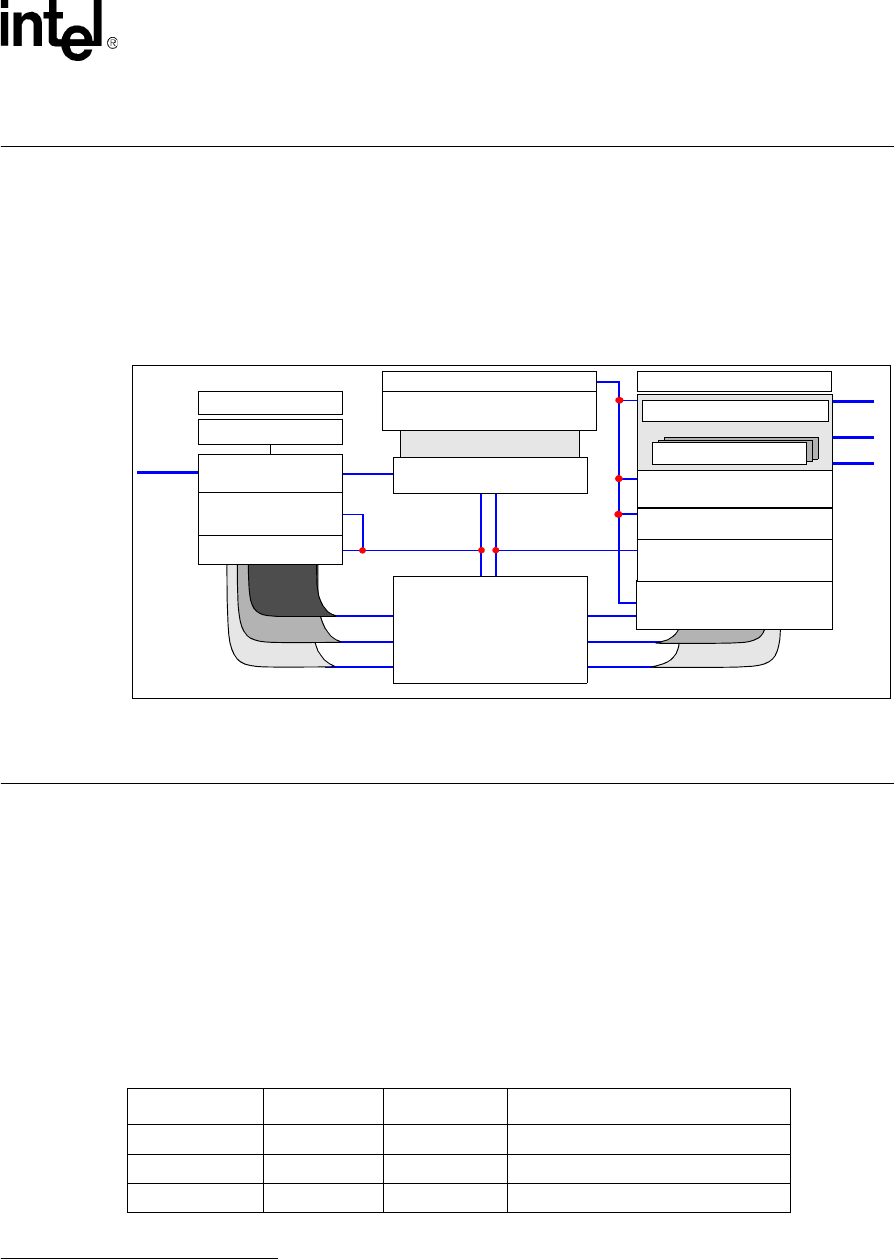
Figure 1. 80960Hx Block Diagram
Execution Unit
Programmable
Bus Controller
Bus Request Queues
Six-Port Register File
32-bit Base Bus
Instruction Cache
128-Bit Cache Bus
Instruction Prefetch Queue
Interrupt Controller
Control
Address
Data
Memory-Side
Machine Bus
Register-Side
Machine Bus
Memory Region Configuration
Multiply/Divide Unit
Interrupt
Port
Address Generation Unit
Data Cache
16 Kbyte, Four-Way Set-Associative
8 Kbyte, Four-Way Set-Associative
Guarded Memory Unit
Timers
JTAG Port
Parallel Instruction Scheduler
Data RAM - 2 Kbyte
Register Cache - 5 to 15 sets
64-bit SRC1 Bus
64-bit SRC2 Bus
64-bit DST Bus
128-bit Load Bus
128-bit Store Bus
1.The 80960Hx is not “drop-in” compatible in an 80960Cx-based system. Customers may design systems that accept either 80960Hx or Cx
processors.
Table 1. 80960Hx Product Description
ProductCoreVoltageOperating Frequency (bus/core)
80960HA 1x3.3V†25/25, 33/33, 40/40
80960HD 2x3.3V†25/50, 33/66, 40/80
80960HT 3x3.3V†25/75
†Processor inputs are 5 V tolerant.

80960HA/HD/HT
10 Datasheet
In addition to expanded clock frequency options, the 80960Hx provides essential enhancements for
an emerging class of high-performance embedded applications. Features include a larger
instruction cache, data cache, and data RAM than any other 80960 processor to date. It also boasts
a 32-bit demultiplexed and pipelined burst bus, fast interrupt mechanism, guarded memory unit,
wait state generator, dual programmable timers, ONCE and IEEE 1149.1-compliant boundary scan
test and debug support, and new instructions.
2.1The i960® Processor Family
The i960® processor family is a 32-bit RISC architecture created by Intel to serve the needs of
embedded applications. The embedded market includes applications as diverse as industrial
automation, avionics, image processing, graphics and communications.
Because all members of the i960 processor family share a common core architecture, i960
applications are code-compatible. Each new processor in the family adds its own special set of
functions to the core to satisfy the needs of a specific application or range of applications in the
embedded market.
2.2Key 80960Hx Features
2.2.1Execution Architecture
Independent instruction paths inside the processor allow the execution of multiple, out-of-sequence
instructions per clock. Register and resource scoreboarding interlocks maintain the logical integrity
of sequential instructions that are being executed in parallel. To sustain execution of multiple
instructions in each clock cycle, the processor decodes multiple instructions in parallel and
simultaneously issues these instructions to parallel processing units. The various processing units
are then able to independently access instruction operands in parallel from a common register set.
Local Register Cache integrated on-chip provides automatic register management on call/return
instructions. Upon a call instruction, the processor allocates a set of local registers for the called
procedure, then stores the registers for the previous procedure in the on-chip register cache. As
additional procedures are called, the cache stores the associated registers such that the most recently
called procedure is the first available by the next return (ret) instruction. The processor may store up
to fifteen register sets, after which the oldest sets are stored (spilled) into external memory.
The 80960Hx supports the 80960 architecturally-defined branch prediction mechanism. This
allows many branches to execute with no pipeline break. With the 80960Hx’s efficient pipeline, a
branch may take as few as zero clocks to execute. The maximum penalty for an incorrect prediction
is two core clocks.
2.2.2Pipelined, Burst Bus
A 32-bit high performance bus controller interfaces the 80960Hx core to the external memory and
peripherals. The Bus Control Unit features a maximum transfer rate of 160 Mbytes per second (at a
40 MHz external bus clock frequency). A key advantage of this design is its versatility. The user
may independently program the physical and logical attributes of system memory. Physical
attributes include wait state profile, bus width, and parity. Logical attributes include cacheability
and Big or Little Endian byte order. Internally programmable wait states and 16 separately
configurable physical memory regions allow the processor to interface with a variety of memory

80960HA/HD/HT
Datasheet11
subsystems with minimum system complexity. To reduce the effect of wait states, the bus design is
decoupled from the core. This lets the processor execute instructions while the bus performs
memory accesses independently.
The Bus Controller’s key features include:
•Demultiplexed, Burst Bus to support most efficient DRAM access modes
•Address Pipelining to reduce memory cost while maintaining performance
•32-, 16- and 8-bit modes to facilitate I/O interfacing
•Full internal wait state generation to reduce system cost
•Little and Big Endian support
•Unaligned Access support implemented in hardware
•Three-deep request queue to decouple the bus from the core
•Independent physical and logical address space characteristics
2.2.3On-Chip Caches and Data RAM
As shown in Figure 1, the 80960Hx provides generous on-chip cache and storage features to
decouple CPU execution from the external bus. The processor includes a 16 Kbyte instruction
cache, an 8 Kbyte data cache and 2 Kbytes of Data RAM. The caches are organized as 4-way set
associative. Stores that hit the data cache are written through to memory. The data cache performs
write allocation on cache misses. A fifteen-set stack frame cache allows the processor to rapidly
allocate and deallocate local registers. All of the on-chip RAM sustains a 4-word (128-bit) access
every clock cycle.
2.2.4Priority Interrupt Controller
The interrupt unit provides the mechanism for the low latency and high throughput interrupt
service essential for embedded applications. A priority interrupt controller provides full
programmability of 240 interrupt sources with a typical interrupt task switch (latency) time of 17
core clocks. The controller supports 31 priority levels. Interrupts are prioritized and signaled within
10 core clocks of the request. When the interrupt has a higher priority than the processor priority,
the context switch to the interrupt routine would typically complete in another seven bus clocks.
External agents post interrupts through the 8-bit external interrupt port. The Interrupt unit also
handles the two internal sources from the Timers. Interrupts may be level- or edge-triggered.
2.2.5Guarded Memory Unit
The Guarded Memory Unit (GMU) provides memory protection without the address translation
found in Memory Management Units. The GMU contains two memory protection schemes: one
prevents illegal memory accesses, the other detects memory access violations. Both signal a fault
to the processor. The programmable protection modes are: user read, write or execute; and
supervisor read, write or execute.

80960HA/HD/HT
12 Datasheet
2.2.6Dual Programmable Timers
The processor provides two independent 32-bit timers, with four programmable clock rates. The
user configures the timers through the Timer Unit registers. These registers are memory-mapped
within the 80960Hx, addressable on 32-bit boundaries. The timers have a single-shot mode and
auto-reload capabilities for continuous operation. Each timer has an independent interrupt request
to the processor’s interrupt controller.
2.2.7Processor Self Test
When a system error is detected, the FAIL pin is asserted, a fail code message is driven onto the
address bus, and the processor stops execution at the point of failure. The only way to resume
normal operation is to perform a RESET operation. Because System Error generation may occur
sometime after the bus confidence test and even after initialization during normal processor
operation, the FAIL pin is HIGH (logic “1”) before the detection of a System Error.
The processor uses only one read bus-transaction to signal the fail code message; the address of the
bus transaction is the fail code itself. The fail code is of the form: 0xfeffffnn; bits 6 to 0 contain a
mask recording the possible failures. Bit 7, when set to 1, indicates that the mask contains failures
from the internal Built-In Self-Test (BIST); when 0, the mask indicates other failures.
Ignore reserved bits 0 and 1. Also ignore bits 5 and 6 when bit 7 is clear (=0).
The mask is shown in Table 2 and Table 3.
Table 2. Fail Codes For BIST (bit 7 = 1)
BitWhen Set
6On-chip Data-RAM failure detected by BIST.
5Internal Microcode ROM failure detected by BIST.
4Instruction cache failure detected by BIST.
3Data cache failure detected by BIST.
2Local-register cache or processor core failure detected by BIST.
1Reserved. Always zero.
0Reserved. Always zero.
Table 3. Remaining Fail Codes (bit 7 = 0)
BitWhen Set
6Reserved. Always one.
5Reserved. Always one.
4A data structure within the IMI is not aligned to a word boundary.
3A System Error during normal operation has occurred.
2The Bus Confidence test has failed.
1Reserved. Always zero.
0Reserved. Always zero.

80960HA/HD/HT
Datasheet13
2.3Instruction Set Summary
Table 4 summarizes the 80960Hx instruction set by logical groupings.
Table 4. 80960Hx Instruction Set
Data MovementArithmeticLogical Bit / Bit Field / Byte
Load
Store
Move
Load Address
Conditional Select2
Add
Subtract
Multiply
Divide
Remainder
Modulo
Shift
Extended Shift
Extended Multiply
Extended Divide
Add with Carry
Subtract with Carry
Rotate
Conditional Add2
Conditional Subtract2
And
Not And
And Not
Or
Exclusive Or
Not Or
Or Not
Nor
Exclusive Nor
Not
Nand
Set Bit
Clear Bit
Not Bit
Alter Bit
Scan For Bit
Span Over Bit
Extract
Modify
Scan Byte for Equal
Byte Swap2
Comparison Branch Call/Return Fault
Compare
Conditional Compare
Compare and Increment
Compare and Decrement
Compare Byte2
Compare Short2
Test Condition Code
Check Bit
Unconditional Branch
Conditional Branch
Compare and Branch
Call
Call Extended
Call System
Return
Branch and Link
Conditional Fault
Synchronize Faults
Debug Processor Mgmt AtomicCache Control
Modify Trace Controls
Mark
Force Mark
Flush Local Registers
Modify Arithmetic Controls
Modify Process Controls
Interrupt Enable/ Disable1, 2
System Control1
Atomic Add
Atomic Modify
Instruction Cache
Control1, 2
Data Cache Control1, 2
NOTES:
1. 80960Hx extensions to the 80960 core instruction set.
2. 80960Hx extensions to the 80960Cx instruction set.
80960HA/HD/HT
14 Datasheet
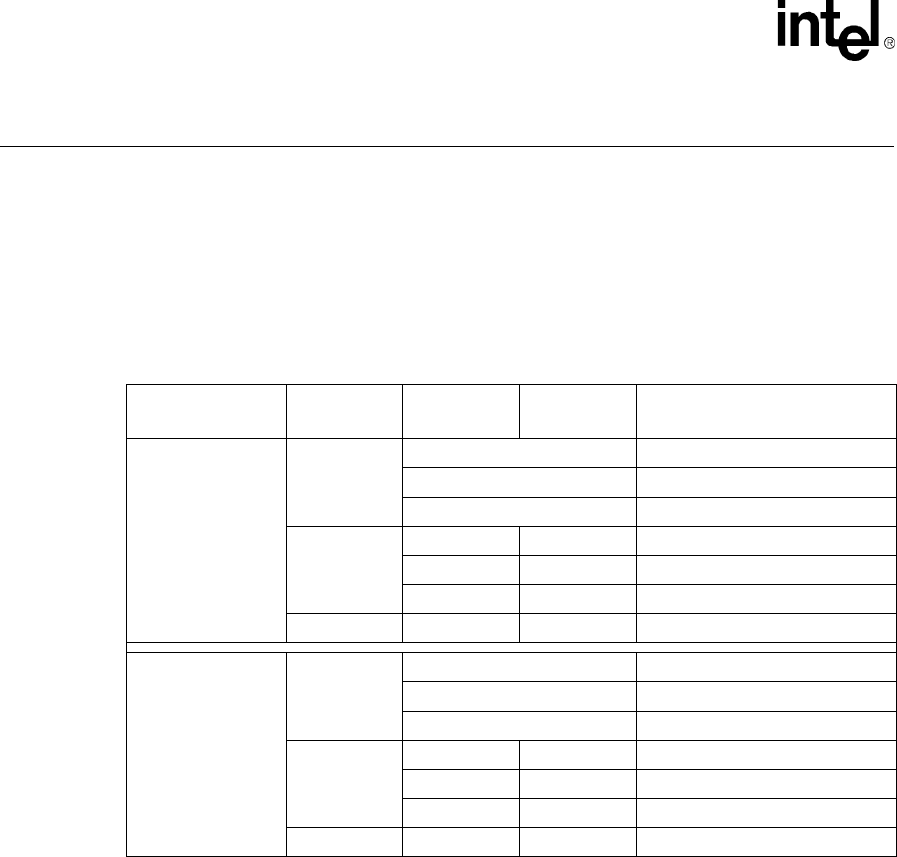
3.0 Package Information
This section describes the pins, pinouts and thermal characteristics for the 80960Hx in the 168-pin
ceramic Pin Grid Array (PGA) package, 208-pin PowerQuad2* (PQ4). For complete package
specifications and information, see the Intel Packaging Handbook (Order# 240800).
The 80960HA/HD/HT is offered with eight speeds and two package types (Table 5). Both the
168-pin ceramic Pin Grid Array (PGA) and the 208-pin PowerQuad2* (PQ4) devices are specified
for operation at VCC =3.3 V±0.15 V over a case temperature range of 0 °C to 85 °C.
Table 5. 80960HA/HD/HT Package Types and Speeds
Package/Name Device Core Speed
(MHz)Bus Speed
(MHz)Order #
168L PGA
80960HA
25 A80960HA25 S L2GX
33 A80960HA33 S L2GY
40 A80960HA40 S L2GZ
80960HD
50 25 A80960HD50 S L2GH
66 33 A80960HD66 S L2GJ
80 40 A80960HD80 S L2GK
80960HT 75 25 A80960HT75 S L2GP
208L PQFP
(also known as PQ4)
80960HA
25 FC80960HA25 S L2GU
33 FC80960HA33 S L2GV
40 FC80960HA40 S L2GW
80960HD
50 25 FC80960HD50 S L2GM
66 33 FC80960HD66 S L2GN
80 40 FC80960HD80 S L2LZ
80960HT 75 25 FC80960HT75 S L2GT

80960HA/HD/HT
Datasheet15
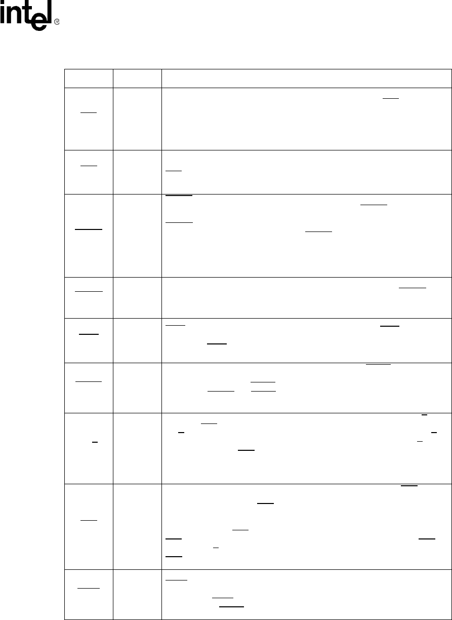
3.1 Pin Descriptions
This section defines the 80960Hx pins. Table 6 presents the legend for interpreting the pin
descriptions in Table 7. All pins float while the processor is in the ONCE mode, except TDO,
which may be driven active according to normal JTAG specifications.
Table 6. Pin Description Nomenclature
SymbolDescription
IInput only pin.
OOutput only pin.
I/OPin may be input or output.
-Pin must be connected as indicated for proper device functionality.
S(E)Synchronous edge sensitive input. This input must meet the setup and hold times relative to
CLKIN to ensure proper operation of the processor.
S(L) Synchronous level sensitive input. This input must meet the setup and hold times relative to
CLKIN to ensure proper operation of the processor.
A(E)Asynchronous edge-sensitive input.
A(L) Asynchronous level-sensitive input.
H(...)
While the processor bus is in the HOLD state (HOLDA asserted), the pin:
H(1) is driven to VCC
H(0) is driven to VSS
H(Z) floats
H(Q) continues to be a valid output
B(...)
While the processor is in the bus backoff state (BOFF asserted), the pin:
B(1) is driven to VCC
B(0) is driven to VSS
B(Z) floats
B(Q) continues to be a valid output
R(...)
While the processor’s RESET pin is asserted, the pin:
R(1) is driven to VCC
R(0) is driven to VSS
R(Z) floats
R(Q) continues to be a valid output

80960HA/HD/HT
16 Datasheet
Table 7. 80960Hx Processor Family Pin Descriptions (Sheet 1 of 4)
Name TypeDescription
A31:2
O
H(Z)
B(Z)
R(Z)
ADDRESS BUS carries the upper 30 bits of the physical address. A31 is the most
significant address bit and A2 is the least significant. During a bus access, A31:2
identify all external addresses to word (4-byte) boundaries. The byte enable
signals indicate the selected byte in each word. During burst accesses, A3 and
A2 increment to indicate successive addresses.
D31:0
I/O
S(L)
H(Z)
B(Z)
R(Z)
DATA BUS carries 32, 16, or 8-bit data quantities depending on bus width
configuration. The least significant bit of the data is carried on D0 and the most
significant on D31. The lower eight data lines (D7:0) are used when the bus is
configured for 8-bit data. When configured for 16-bit data, D15:0 are used.
DP3:0
I/O
S(L)
H(Z)
B(Z)
R(Z)
DATA PARITY carries parity information for the data bus. Each parity bit is
assigned a group of eight data bus pins as follows:
DP3 generates/checks parity for D31:24
DP2 generates/checks parity for D23:16
DP1 generates/checks parity for D15:8
DP0 generates/checks parity for D7:0
Parity information is generated for a processor write cycle and is checked for a
processor read cycle. Parity checking and polarity are programmable. Parity
generation/checking is only performed for the size of the data accessed.
PCHK
O
H(Q)
B(Q)
R(1)
PARITY CHECK indicates the result of a parity check operation. An asserted
PCHK indicates that the previous bus read access resulted in a parity check error.
BE3:0
O
H(Z)
B(Z)
R(1)
BYTE ENABLES select which of the four bytes addressed by A31:2 are active
during a bus access. Byte enable encoding is dependent on the bus width of the
memory region accessed:
32-bit bus:
BE3 enables D31:24
BE2 enables D23:16
BE1 enables D15:8
BE0 enables D7:0
16-bit bus:
BE3 becomes Byte High Enable (enables D15:8)
BE2 is not used (state is undefined)
BE1 becomes Address Bit 1 (A1)
BE0 becomes Byte Low Enable (enables D7:0)
8-bit bus:
BE3 is not used (state is undefined)
BE2 is not used (state is undefined)
BE1 Address Bit 1 (A1)
BE0 Address Bit 0 (A0)
W/R
O
H(Z)
B(Z)
R(0)
WRITE/READ is low for read accesses and high for write accesses.
W/R becomes valid during the address phase of a bus cycle and remains valid
until the end of the cycle for non-pipelined accesses. For pipelined accesses, W/
R changes state when the next address is presented.
0= Read
1= Write
D/C
O
H(Z)
B(Z)
R(0)
DATA/CODE indicates that a bus access is a data access or an instruction
access. D/C has the same timing as W/R.
0 = Code
1 = Data
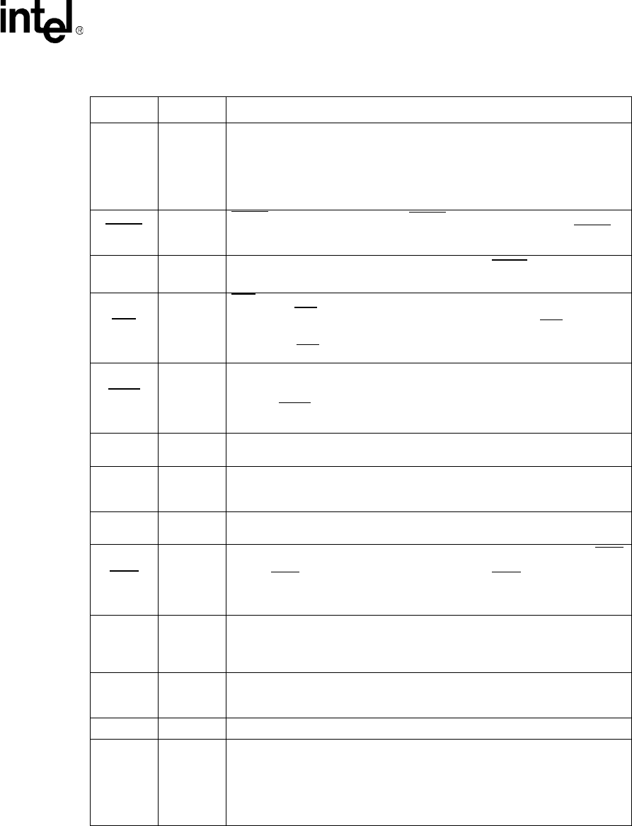
80960HA/HD/HT
Datasheet17
SUP
O
H(Z)
B(Z)
R(1)
SUPERVISOR ACCESS indicates whether the current bus access originates
from a request issued while in supervisor mode or user mode. SUP may be used
by the memory subsystem to isolate supervisor code and data structures from
non-supervisor access.
0 = Supervisor Mode
1 = User Mode
ADS
O
H(Z)
B(Z)
R(1)
ADDRESS STROBE indicates a valid address and the start of a new bus access.
ADS is asserted for the first clock of a bus access.
READYI
S(L)
READY, when enabled for a memory region, is asserted by the memory
subsystem to indicate the completion of a data transfer. READY is used to
indicate that read data on the bus is valid, or that a write transfer has completed.
READY works in conjunction with the internal wait state generator to
accommodate various memory speeds. READY is sampled after any
programmed wait states:
During each data cycle of a burst access
During the data cycle of a non-burst access
BTERMI
S(L)
BURST TERMINATE, when enabled for a memory region, is asserted by the
memory subsystem to terminate a burst access in progress. When BTERM is
asserted, the current burst access is terminated and another address cycle
occurs.
WAIT
O
H(Z)
B(Z)
R(1)
WAIT indicates the status of the internal wait-state generator. WAIT is asserted
when the internal wait state generator generates NWAD, NRAD, NWDD and NRDD
wait states. WAIT may be used to derive a write data strobe.
BLAST
O
H(Z)
B(Z)
R(1)
BURST LAST indicates the last transfer in a bus access. BLAST is asserted in
the last data transfer of burst and non-burst accesses after the internal wait-state
generator reaches zero. BLAST remains active as long as wait states are inserted
through the READY pin. BLAST becomes inactive after the final data transfer in a
bus cycle.
DT/R
O
H(Z)
B(Z)
R(0)
DATA TRANSMIT/RECEIVE indicates direction for data transceivers. DT/R is
used with DEN to provide control for data transceivers connected to the data bus.
DT/R is driven low to indicate the processor expects data (a read cycle). DT/R is
driven high when the processor is “transmitting” data (a store cycle). DT/R only
changes state when DEN is high.
0 = Data Receive
1 = Data Transmit
DEN
O
H(Z)
B(Z)
R(1)
DATA ENABLE indicates data transfer cycles during a bus access. DEN is
asserted at the start of the first data cycle in a bus access and de-asserted at the
end of the last data cycle. DEN remains asserted for an entire bus request, even
when that request spans several bus accesses. For example, a ldq instruction
starting at an unaligned quad word boundary is one bus request spanning at least
two bus accesses. DEN remains asserted throughout all the accesses (including
ADS states) and de-asserts when the Iqd instruction request is satisfied. DEN is
used with DT/R to provide control for data transceivers connected to the data bus.
DEN remains asserted for sequential reads from pipelined memory regions.
LOCK
O
H(Z)
B(Z)
R(1)
BUS LOCK indicates that an atomic read-modify-write operation is in progress.
LOCK may be used by the memory subsystem to prevent external agents from
accessing memory that is currently involved in an atomic operation (e.g., a
semaphore). LOCK is asserted in the first clock of an atomic operation and de-
asserted when BLAST is deasserted in the last bus cycle.
Table 7. 80960Hx Processor Family Pin Descriptions (Sheet 2 of 4)
Name TypeDescription

80960HA/HD/HT
18 Datasheet
HOLD I
S(L)
HOLD REQUEST signals that an external agent requests access to the
processor’s address, data, and control buses. When HOLD is asserted, the
processor:
Completes the current bus request.
Asserts HOLDA and floats the address, data, and control buses.
When HOLD is deasserted, the HOLDA pin is deasserted and the processor
reassumes control of the address, data, and control pins.
HOLDA
O
H(1)
B(0)
R(Q)
HOLD ACKNOWLEDGE indicates to an external master that the processor has
relinquished control of the bus. The processor grants HOLD requests and enters
the HOLDA state while the RESET pin is asserted.
HOLDA is never granted while LOCK is asserted.
BOFF I
S(L)
BUS BACKOFF forces the processor to immediately relinquish control of the bus
on the next clock cycle. When READY/BTERM is enabled and:
When BOFF is asserted, the address, data, and control buses are floated on the
next clock cycle and the current access is aborted.
When BOFF is deasserted, the processor resumes by regenerating the aborted
bus access.
See Figure 16 on page 48 for BOFF timing requirements.
BREQ
O
H(Q)
B(Q)
R(0)
BUS REQUEST indicates that a bus request is pending in the bus controller.
BREQ does not indicate whether or not the processor is stalled. See BSTALL for
processor stall status. BREQ may be used with BSTALL to indicate to an external
bus arbiter the processor’s bus ownership requirements.
BSTALL
O
H(Q)
B(Q)
R(0)
BUS STALL indicates that the processor has stalled pending the result of a
request in the bus controller. When BSTALL is asserted, the processor must
regain bus ownership to continue processing (i.e., it may no longer execute
strictly out of on-chip cache memory).
CT3:0
O
H(Z)
B(Z)
R(Z)
CYCLE TYPE indicates the type of bus cycle currently being started or processor
state. CT3:0 encoding follows:
Cycle TypeADSCT3:0
Program-initiated access using 8-bit bus00000
Program-initiated access using 16-bit bus00001
Program-initiated access using 32-bit bus00010
Event-initiated access using 8-bit bus 00100
Event-initiated access using 16-bit bus 00101
Event-initiated access using 32-bit bus 00110
Reserved 00X11
Reserved for future products01XXX
Reserved 1XXXX
XINT7:0
I
A(E)
A(L)
EXTERNAL INTERRUPT pins are used to request interrupt service. These pins
may be configured in three modes:
Dedicated Mode: Each pin is assigned a dedicated interrupt level. Dedicated
inputs may be programmed to be level (low or high) or edge (rising or falling)
sensitive.
Expanded Mode: All eight pins act as a vectored interrupt source. The interrupt
pins are level sensitive in this mode.
Mixed Mode: The XINT7:5 pins act as dedicated sources and the XINT4:0 pins
act as the five most significant bits of a vectored source. The least significant bits
of the vectored source are set to “010” internally.
NMI I
A(E)
NON-MASKABLE INTERRUPT causes a non-maskable interrupt event to occur.
NMI is the highest priority interrupt source. NMI is falling edge triggered.
Table 7. 80960Hx Processor Family Pin Descriptions (Sheet 3 of 4)
Name TypeDescription
80960HA/HD/HT
Datasheet19
CLKINI
CLOCK INPUT provides the time base for the 80960Hx. All internal circuitry is
synchronized to CLKIN. All input and output timings are specified relative to
CLKIN.
For the 80960HD, the 2x internal clock is derived by multiplying the CLKIN
frequency by two. For the 80960HT, the 3x internal clock is derived by multiplying
the CLKIN frequency by three.
RESETI
A(L)
RESET forces the device into reset. RESET causes all external and internal
signals to return to their reset state (when defined). The rising edge of RESET
starts the processor boot sequence.
STESTI
S(L)
SELF TEST, when asserted during the rising edge of RESET, causes the
processor to execute its built in self-test.
FAIL
O
H(Q)
B(Q)
R(0)
FAIL indicates a failure of the processor’s built-in self-test performed during
initialization. FAIL is asserted immediately out of reset and toggles during self-test
to indicate the status of individual tests. When self-test passes, FAIL is de-
asserted and the processor branches to the user’s initialization code. When self-
test fails, the FAIL pin asserts and the processor ceases execution.
ONCE I
ON-CIRCUIT EMULATION control: the processor samples this pin during reset.
When it is asserted low at the end of reset, the processor enters ONCE mode. In
ONCE mode, the processor stops all clocks and floats all output pins except the
TDO pin. ONCE uses an internal pull-up resistor; see RPU definition in Table 22,
“80960Hx DC Characteristics” on page 40. Pull this pin high when not in use.
TCK ITEST CLOCK provides the clocking function for IEEE 1149.1 Boundary Scan
testing.
TDI I TEST DATA INPUT is the serial input pin for IEEE 1149.1 Boundary Scan testing.
TDI uses an internal pull-up resistor; see RPU definition in Table 22, “80960Hx DC
Characteristics” on page 40.
TDO OTEST DATA OUTPUT is the serial output pin for IEEE 1149.1 Boundary Scan
testing. ONCE does not disable this pin.
TRST I
TEST RESET asynchronously resets the Test Access Port (TAP) controller. TRST
must be held low at least 10,000 clock cycles after power-up. One method is to
provide TRST with a separate power-on-reset circuit. TRST includes an internal
pull-up resistor; see RPU definition in Table 22, “80960Hx DC Characteristics” on
page 40. Pull this pin low when not in use.
TMSI
TEST MODE SELECT is sampled at the rising edge of TCK. TCK controls the
sequence of TAP controller state changes for IEEE 1149.1 Boundary Scan
testing. TMS uses an internal pull-up resistor; see RPU definition in Table 22,
“80960Hx DC Characteristics” on page 40.
VCC5 I5V REFERENCE VOLTAGE input is the reference voltage for the 5 V-tolerant I/O
buffers. Connect this signal to +5 V for use with inputs which exceed 3.3V. When
all inputs are from 3.3V components, connect this signal to 3.3V.
VCCPLL IPLL VOLTAGE is the +3.3VDC analog input for the PLL.
VOLDET O
VOLTAGE DETECT signal allows external system logic to distinguish between a
5V 80960Cx processor and the 3.3V 80960Hx processor. This signal is active
low for a 3.3V 80960Hx (it is high impedance for 5 V 80960Cx). This pin is
available only on the PGA version.
0 = 80960Hx
1 = 80960Cx
Table 7. 80960Hx Processor Family Pin Descriptions (Sheet 4 of 4)
Name TypeDescription
80960HA/HD/HT
20 Datasheet
3.2 80960Hx Mechanical Data
3.2.180960Hx PGA Pinout
Figure 2 depicts the complete 80960Hx PGA pinout as viewed from the top side of the component
(i.e., pins facing down). Figure 3 shows the complete 80960Hx PGA pinout as viewed from the
pin-side of the package (i.e., pins facing up). Table 9 lists the 80960Hx pin names with package
location. See Section 4.3, “Recommended Connections” on page 38 for specifications and
recommended connections.
Figure 2. 80960Hx 168-Pin PGA Pinout—View from Top (Pins Facing Down)
D5D7D8D9D11D12D13D15D16D17D19D21D24D25
D2D4D6VCC
D10VCC
VCC
D14VCC
D18D20D23D27D29
NCD0VCC
VSS
VSS
VSS
VSS
VSS
VSS
VCC
D22D31READYD26
D28BTERM
HOLDA
D30HOLD
BE3
VCC
ADSBE2
VSS
VCC
BE1
VSS
VCC
BLAST
VSS
BE0
DEN
VSS
VCC
W/R
VSS
VCC
DT/R
A29LOCK
SUPWAITBSTALL
A28
A30BREQD/C
D3
D1
ONCE
VSS
VCC5
VCC
VSS
VSS
VSS
VSS
VSS
CLKIN
VCC
VSS
BOFF
STEST
DP1
DP3
TCK
TMS
VCC
PCHK
VCC
VCCPLL
VCC
NC
NC
VCC
VSS
FAIL
DP0
DP2
VOLDET
TRST
TDI
TDO
NC
NC
CTO
CT2
CT3
CT1
VSS
A2
VCC
A22A25
A20VSS
A3A5
NMIVCC
VSS
VSS
VSS
VSS VSS
A24A31A26
A4VCC
A6A8A9A10A11A12A14A15A17A18
VCC
VCC
VCC
A13VCC
A16A19A21A23A27A7 XINT6
XINT7
XINT4
XINT3
XINT5
XINT0
RESET
XINT2
XINT1
1
2
3
4
5
6
7
8
9
10
11
12
13
14
15
16
17
1
2
3
4
5
6
7
8
9
10
11
12
13
14
15
16
17
ABCDEFGHJKLMNPQRS
ABCDEFGHJKLMNPQRS
i©19xx
A80960Hx
XXXXXXXX SS
M
80960HA/HD/HT
Datasheet21
Figure 3. 80960Hx 168-Pin PGA Pinout—View from Bottom (Pins Facing Up)
D5 D7 D8 D9 D11D12 D13 D15 D16 D17 D19 D21 D24 D25
D2 D4 D6 VCC D10 VCC VCC D14 VCC D18D20 D23 D27 D29
NC D0 VCC VSS VSS VSS VSS VSS VSS VCC D22 D31 READY
D26
D28 BTERM HOLDA
D30 HOLDBE3
VCC ADS BE2
VSS VCC BE1
VSS VCC BLAST
VSS BE0 DEN
VSS VCC W/R
VSS VCC DT/R
A29 LOCK
SUPWAITBSTALL
A28
A30BREQD/C
D3
D1
ONCE
VSS
VCC5
VCC
VSS
VSS
VSS
VSS
VSS
CLKIN
VCC
VSS
BOFF
STEST
DP1
DP3
TCK
TMS
VCC
PCHK
VCC
VCCPLL
VCC
NC
NC
VCC
VSS
FAIL
DP0
DP2
VOLDET
TRST
TDI
TDO
NC
NC
CT0
CT2
CT3
CT1
VSS
A2
VCC
A22A25
A20VSS
A3 A5
NMIVCC VSS VSS VSS VSS
VSS A24A31A26
A4 VCC
A6 A8A9 A10A11 A12 A14 A15 A17 A18
VCC VCC VCC A13VCC A16A19 A21 A23A27A7
XINT6
XINT7
XINT4
XINT3
XINT5
XINT0
RESET
XINT2
XINT1
1
2
3
4
5
6
7
8
9
10
11
12
13
14
15
16
17
1
2
3
4
5
6
7
8
9
10
11
12
13
14
15
16
17
ABCDEFGHJKLMNPQRS
ABCDEFGHJKLMNPQRS
Package Lid

80960HA/HD/HT
22 Datasheet
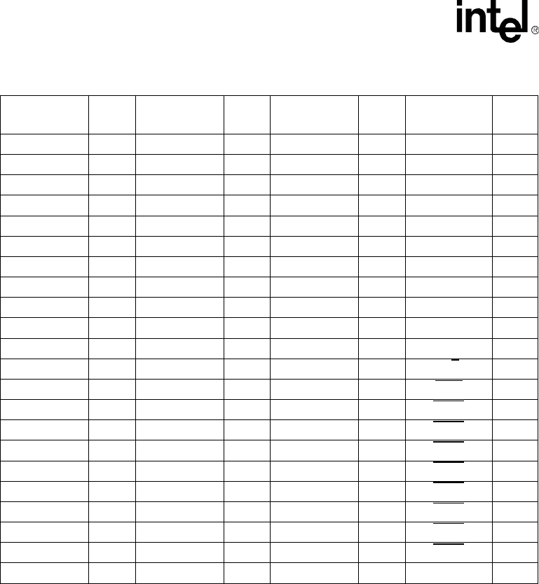
Table 8. 80960Hx 168-Pin PGA Pinout—Signal Name Order (Sheet 1 of 2)
Signal NamePGA
PinSignal NamePGA
PinSignal NamePGA
PinSignal NamePGA
Pin
A2 D16 ADS R6 D14 L2 LOCK S14
A3 D17 BE0R9 D15 L1 NC A9
A4 E16 BE1S7 D16 M1 NC A10
A5 E17 BE2S6 D17 N1 NC B13
A6 F17BE3S5 D18 N2 NC B14
A7 G16BLASTS8 D19 P1 NC D3
A8 G17BOFFB1 D20 P2 NMID15
A9 H17 BREQR13 D21 Q1 ONCE C3
A10 J17 BSTALL R12 D22 P3 PCHK B8
A11K17 BTERMR4 D23 Q2 READYS3
A12 L17 CLKIN C13 D24 R1 RESETA16
A13 L16 CT0A11D25 S1 STESTB2
A14 M17CT1A12 D26 Q3 SUPQ12
A15 N17 CT2A13 D27 R2 TCK B5
A16 N16 CT3A14 D28 Q4 TDIA7
A17 P17 D/C S13 D29 S2 TDO A8
A18 Q17D0 E3 D30 Q5 TMSB6
A19 P16 D1 C2 D31 R3 TRST A6
A20 P15 D2 D2 DENS9 VCC B7
A21 Q16D3 C1 DP0A3 VCC B9
A22 R17 D4 E2 DP1B3 VCC B11
A23 R16 D5 D1 DP2A4 VCC B12
A24 Q15D6 F2 DP3B4 VCC C6
A25 S17 D7 E1 DT/R S11VCC C14
A26 R15 D8 F1 FAILA2 VCC E15
A27 S16 D9 G1 ——VCC F3
A28 Q14D10 H2 ——VCC F16
A29 R14 D11H1 ——VCC G2
A30 Q13D12 J1 HOLD R5 VCC H16
A31 S15 D13 K1 HOLDA S4 VCC J2

80960HA/HD/HT
Datasheet23
VCC J16 VCCPLL B10VSS H3 VSS Q10
VCC K2 VOLDET A5 VSS H15VSS Q11
VCC K16VSS A1 VSS J3 W/R S10
VCC M2 VSS C4 VSS J15 WAITS12
VCC M16 VSS C7 VSS K3 XINT0B15
VCC N3 VSS C8 VSS K15XINT1A15
VCC N15VSS C9 VSS L3 XINT2A17
VCC Q6 VSS C10VSS L15 XINT3B16
VCC R7 VSS C11VSS M3 XINT4C15
VCC R8 VSS C12VSS M15 XINT5B17
VCC R10VSS F15VSS Q7 XINT6C16
VCC R11VSS G3 VSS Q8 XINT7C17
VCC5 C5 VSS G15VSS Q9 ——
Table 8. 80960Hx 168-Pin PGA Pinout—Signal Name Order (Sheet 2 of 2)
Signal NamePGA
PinSignal NamePGA
PinSignal NamePGA
PinSignal NamePGA
Pin

80960HA/HD/HT
24 Datasheet
Table 9. 80960Hx 168-Pin PGA Pinout—Pin Number Order (Sheet 1 of 2)
PGA
PinSignal NamePGA
PinSignal NamePGA
PinSignal NamePGA
PinSignal Name
A1 VSS B14 NC E15 VCC K15 VSS
A2 FAILB15 XINT0E16 A4 K16 VCC
A3 DP0B16 XINT3E17 A5 K17 A11
A4 DP2B17 XINT5F1 D8 L1 D15
A5 VOLDETC1 D3 F2 D6 L2 D14
A6 TRSTC2 D1 F3 VCC L3 VSS
A7 TDI C3 ONCE F15VSS L15VSS
A8 TDO C4 VSS F16VCC L16A13
A9 NC C5 VCC5 F17A6 L17A12
A10 NC C6 VCC G1 D9 M1 D16
A11CT0 C7 VSS G2 VCC M2 VCC
A12 CT1 C8 VSS G3 VSS M3 VSS
A13 CT2 C9 VSS G15VSS M15VSS
A14 CT3 C10 VSS G16A7 M16VCC
A15 XINT1C11VSS G17A8 M17A14
A16 RESETC12 VSS H1 D11N1 D17
A17 XINT2C13 CLKINH2 D10 N2 D18
B1 BOFF C14 VCC H3 VSS N3 VCC
B2 STESTC15 XINT4H15 VSS N15 VCC
B3 DP1C16 XINT6H16 VCC N16 A16
B4 DP3C17 XINT7H17 A9 N17 A15
B5 TCK D1 D5 J1 D12 P1 D19
B6 TMSD2 D2 J2 VCC P2 D20
B7 VCC D3 NC J3 VSS P3 D22
B8 PCHK D15 NMI J15 VSS P15 A20
B9 VCC D16 A2 J16 VCC P16 A19
B10 VCCPLL D17 A3 J17 A10P17 A17
B11VCC E1 D7 K1 D13 Q1 D21
B12 VCC E2 D4 K2 VCC Q2 D23
B13 NC E3 D0 K3 VSS Q3 D26

80960HA/HD/HT
Datasheet25
Q4 D28 Q16A21R11VCC S6 BE2
Q5 D30 Q17A18R12 BSTALL S7 BE1
Q6 VCC R1 D24 R13 BREQ S8 BLAST
Q7 VSS R2 D27 R14 A29S9 DEN
Q8 VSS R3 D31 R15 A26S10 W/R
Q9 VSS R4 BTERMR16 A23S11DT/R
Q10VSS R5 HOLD R17 A22S12 WAIT
Q11VSS R6 ADSS1 D25 S13 D/C
Q12SUPR7 VCC S2 D29 S14 LOCK
Q13A30R8 VCC S3 READYS15 A31
Q14A28R9 BE0S4 HOLDA S16 A27
Q15A24R10 VCC S5 BE3S17 A25
Table 9. 80960Hx 168-Pin PGA Pinout—Pin Number Order (Sheet 2 of 2)
PGA
PinSignal NamePGA
PinSignal NamePGA
PinSignal NamePGA
PinSignal Name

80960HA/HD/HT
26 Datasheet
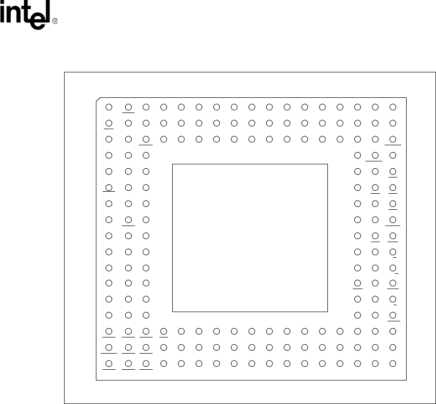
3.2.280960Hx PQ4 Pinout
Figure 4. 80960Hx 208-Pin PQ4 Pinout
PIN 1
PIN 208
PIN 52
PIN 53
PIN 104
PIN 157
PIN 156
VCC
VSS
VSS
VCC
FAIL
ONCE
VSS
VCC
BOFF
VCC
D0
D1
D2
D3
VSS
VCC
VSS
VCC
D4
D5
D6
D7
VSS
VCC
D8
D9
D10
VCC
VSS
VCC
D12
D13
D14
D15
VCC
D16
D17
D18
D19
VSS
VCC
D21
D22
D23
PIN 105
VSS
D24
D25
D26
D27
VSS
VCC
VCC
D28
D29
D30
D31
VSS
VCC
BTERM
READY
HOLD
HOLDA
VSS
VCC
VSS
VCC
VSS
VCC
ADS
BE3
BE2
VSS
VCC
BE1
BE0
BLAST
DEN
VSS
VCC
W/R
DT/R
WAIT
BSTALL
VCC
VSS
VSS
VCC
D/C
SUP
VSS
LOCK
BREQ
VCC
VCC
VSS
VSS
VSS
VCC
VCC
VSS
A2
A3
VCC
VSS
A4
A5
A6
A7
VCC
VSS
A8
A9
A10
A11
VCC
VSS
A12
A13
A14
A15
VCC
VSS
VSS
VCC
A16
A17
A18
A19
VCC
VSS
A20
A21
A22
A23
VCC
VSS
VCC
VSS
A24
A25
A26
A27
VCC
VSS
A28
A29
A30
VSS
VCC
NMI
XINT7
XINT6
XINT5
XINT4
VSS
VCC
XINT3
XINT2
XINT1
XINT0
VSS
VCC
VSS
VCC
RESET
CLKIN
VCCPLL
VSS
VCC
CT3
CT2
CT1
CT0
VSS
VCC
VSS
VCC
TDO
PCHK
VSS
TDI
TMS
TRST
TCK
VSS
VCC
VCC5
VCC
VSS
VCC
DP3
DP2
VCC
VSS
DP0
DP1
STEST
D11
VSS
A31
VSS
VCC
D20
VCC
VSS
VSS iXXXXXXXX SS
M ©19xx
i960®
FC80960Hx
VCC
VSS

80960HA/HD/HT
Datasheet27
Table 10. 80960Hx PQ4 Pinout—Signal Name Order (Sheet 1 of 2)
Signal NamePQ4
PinSignal NamePQ4
PinSignal NamePQ4
PinSignal NamePQ4
Pin
A2 151 BE083 D16 39 PCHK 189
A3 150 BE182 D17 40 READY 68
A4 147 BE279 D18 41 RESET174
A5 146 BE378 D19 42 STEST208
A6 145 BLAST84 D20 45 SUP97
A7 144 BOFF 10 D21 50 TCK194
A8 141 BREQ100 D22 51 TDI 191
A9 140 BSTALL 91 D23 52 TDO188
A10 139 BTERM67 D24 54 TMS192
A11138 CLKIN 175 D25 55 TRST193
A12 135 CT0 183 D26 56 VCC 1
A13 134 CT1 182 D27 57 VCC 4
A14 133 CT2 181 D28 61 VCC 9
A15 132 CT3 180 D29 62 VCC 11
A16 127 D/C96 D30 63 VCC 17
A17 126 D0 12 D31 64 VCC 19
A18 125 D1 13 DEN85 VCC 25
A19 124 D2 14 DP0206 VCC 31
A20 121 D3 15 DP1207 VCC 33
A21 120 D4 20 DP2203 VCC 38
A22 119 D5 21 DP3202 VCC 44
A23 118 D6 22 DT/R 89 VCC 46
A24 113 D7 23 FAIL5VCC 49
A25 112 D8 26 ——VCC 59
A26 111 D9 27 ——VCC 60
A27 110 D10 28 ——VCC 66
A28 107 D1129 HOLD69 VCC 71
A29 106 D12 34 HOLDA 72 VCC 74
A30 105 D13 35 LOCK 99 VCC 76
A31 104 D14 36 NMI159 VCC 81
ADS 77 D15 37 ONCE 6VCC 87
80960HA/HD/HT
28 Datasheet
VCC 92 VCC 187 VSS 70 VSS 164
VCC 95 VCC 196 VSS 73 VSS 170
VCC 101 VCC 199 VSS 75 VSS 172
VCC 102 VCC 201 VSS 80 VSS 178
VCC 109 VCC 204 VSS 86 VSS 184
VCC 115 VCC5 197 VSS 93 VSS 186
VCC 117 VCCPLL 177 VSS 94 VSS 190
VCC 123 VSS 2VSS 98 VSS 195
VCC 128 VSS 3VSS 103 VSS 198
VCC 131 VSS 7V
SS 108 VSS 200
VCC 137 VSS 8VSS 114 VSS 205
VCC 143 VSS 16 VSS 116 W/R88
VCC 149 VSS 18 VSS 122 WAIT90
VCC 153 VSS 24 VSS 129 XINT0169
VCC 154 VSS 30 VSS 130 XINT1168
VCC 158 VSS 32 VSS 136 XINT2167
VCC 165 VSS 43 VSS 142 XINT3166
VCC 171 VSS 47 VSS 148 XINT4163
VCC 173 VSS 48 VSS 152 XINT5162
VCC 176 VSS 53 VSS 155 XINT6161
VCC 179 VSS 58 VSS 156 XINT7160
VCC 185 VSS 65 VSS 157 ——
Table 10. 80960Hx PQ4 Pinout—Signal Name Order (Sheet 2 of 2)
Signal NamePQ4
PinSignal NamePQ4
PinSignal NamePQ4
PinSignal NamePQ4
Pin

80960HA/HD/HT
Datasheet29
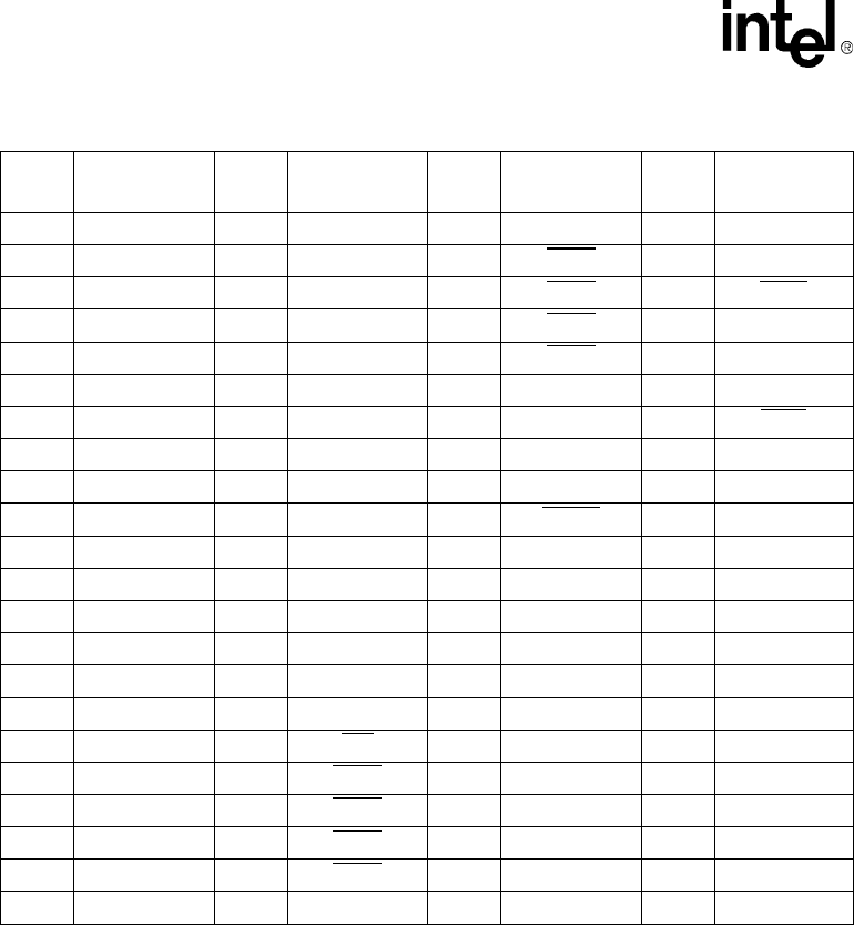
Table 11. 80960Hx PQ4 Pinout—Pin Number Order (Sheet 1 of 2)
PQ4
PinSignal NamePQ4
PinSignal NamePQ4
PinSignal NamePQ4
PinSignal Name
1VCC 31 VCC 61 D28 91 BSTALL
2VSS 32 VSS 62 D29 92 VCC
3VSS 33 VCC 63 D30 93 VSS
4VCC 34 D12 64 D31 94 VSS
5FAIL 35 D13 65 VSS 95 VCC
6ONCE 36 D14 66 VCC 96 D/C
7VSS 37 D15 67 BTERM97 SUP
8VSS 38 VCC 68 READY98 VSS
9VCC 39 D16 69 HOLD 99 LOCK
10 BOFF40 D17 70 VSS 100 BREQ
11 VCC 41 D18 71 VCC 101 VCC
12 D0 42 D19 72 HOLDA 102 VCC
13 D1 43 VSS 73 VSS 103 VSS
14 D2 44 VCC 74 VCC 104 A31
15 D3 45 D20 75 VSS 105 A30
16 VSS 46 VCC 76 VCC 106 A29
17 VCC 47 VSS 77 ADS107 A28
18 VSS 48 VSS 78 BE3108 VSS
19 VCC 49 VCC 79 BE2109 VCC
20 D4 50 D21 80 VSS 110 A27
21 D5 51 D22 81 VCC 111 A26
22 D6 52 D23 82 BE1112 A25
23 D7 53 VSS 83 BE0113 A24
24 VSS 54 D24 84 BLAST114 VSS
25 VCC 55 D25 85 DEN115 VCC
26 D8 56 D26 86 VSS 116 VSS
27 D9 57 D27 87 VCC 117 VCC
28 D10 58 VSS 88 W/R118 A23
29 D1159 VCC 89 DT/R 119 A22
30 VSS 60 VCC 90 WAIT120 A21
80960HA/HD/HT
30 Datasheet
121 A20143 VCC 165 VCC 187 VCC
122 VSS 144 A7 166 XINT3188 TDO
123 VCC 145 A6 167 XINT2189 PCHK
124 A19146 A5 168 XINT1190 VSS
125 A18147 A4 169 XINT0191 TDI
126 A17148 VSS 170 VSS 192 TMS
127 A16149 VCC 171 VCC 193 TRST
128 VCC 150 A3 172 VSS 194 TCK
129 VSS 151 A2 173 VCC 195 VSS
130 VSS 152 VSS 174 RESET196 VCC
131 VCC 153 VCC 175 CLKIN197 VCC5
132 A15154 VCC 176 VCC 198 VSS
133 A14155 VSS 177 VCCPLL 199 VCC
134 A13156 VSS 178 VSS 200 VSS
135 A12157 VSS 179 VCC 201 VCC
136 VSS 158 VCC 180 CT3 202 DP3
137 VCC 159 NMI 181 CT2 203 DP2
138 A11160 XINT7182 CT1 204 VCC
139 A10161 XINT6183 CT0 205 VSS
140 A9 162 XINT5184 VSS 206 DP0
141 A8 163 XINT4185 VCC 207 DP1
142 VSS 164 VSS 186 VSS 208 STEST
Table 11. 80960Hx PQ4 Pinout—Pin Number Order (Sheet 2 of 2)
PQ4
PinSignal NamePQ4
PinSignal NamePQ4
PinSignal NamePQ4
PinSignal Name
80960HA/HD/HT
Datasheet31
3.3 Package Thermal Specifications
The 80960Hx is specified for operation when TC (case temperature) is within the range of
0 °C to 85 °C. TC may be measured in any environment to determine whether the 80960Hx is
within the specified operating range. Measure the case temperature at the center of the top surface,
opposite the pins. Refer to Figure 5.
TA (ambient temperature) is calculated from θCA (thermal resistance from case to ambient) using
Equation 1:
Equation 1. Calculation of Ambient Temperature (TA)
Table 12 shows the maximum TA allowable (without exceeding TC) at various airflows and
operating frequencies (fCLKIN).
Note that TA is greatly improved by attaching fins or a heatsink to the package. P (maximum power
consumption) is calculated by using the typical ICC as tabulated in Section 4.6, “DC
Specifications” on page40 and VCC of 3.3 V.
TATCPθCA
⋅()–=
Figure 5. Measuring 80960Hx PGA Case Temperature
Measure PGA/PQ4 temperature at
center of top surface
80960HA/HD/HT
32 Datasheet
Table 12. Maximum TA at Various Airflows in ° C (PGA Package Only)
Airflow-ft/min (m/sec)
fCLKIN
(MHz)0
(0) 200
(1.01) 400
(2.03) 600
(3.04) 800
(4.06) 1000
(5.07)
Core
1X Bus
Clock
TA with
Heatsink†
25
33
40
69
63
59
74
70
67
78
75
73
79
77
75
80
79
77
80
79
77
TA
without
Heatsink
25
33
40
64
56
50
67
62
56
71
67
63
74
70
67
75
72
69
76
74
71
Core
2X Bus
Clock
TA with
Heatsink†
16
25
33
40
68
58
49
41
73
66
60
55
77
73
69
65
79
75
71
68
80
77
74
72
80
77
74
72
TA
without
Heatsink
16
25
33
40
62
49
38
27
66
56
46
38
71
62
55
48
73
66
60
55
75
68
63
58
76
71
66
62
Core
3X Bus
Clock
TA with
Heatsink†20
25 53
45 63
58 71
67 73
70 76
73 76
73
TA
without
Heatsink
20
25 43
33 51
42 58
51 63
58 66
61 68
64
†*0.285” high unidirectional heatsink (AI alloy 6061, 50 mil fin width, 150 mil center-to-center fin spacing).
Table 13. 80960Hx 168-Pin PGA Package Thermal Characteristics
Thermal Resistance — ° C/Watt
Parameter
Airflow — ft./min (m/sec)
0
(0)200
(1.01) 400
(2.03) 600
(3.07) 800
(4.06) 1000
(5.07)
θ Junction-to-Case
(Case measured as
shown in Figure 5.) 1.5 1.51.5 1.51.5 1.5
θ Case-to-Ambient
(No Heatsink) 17 14 11 9 8 7
θ Case-to-Ambient
(With Heatsink)31396544
NOTES:
1. This table applies to 80960Hx PGA plugged into socket or soldered directly to board.
2. θJA = θJC + θCA
3. 0.285” high unidirectional heatsink (AI alloy 6061, 50 mil fin width, 150 mil center-to-center fin spacing).
θJC
θJA
80960HA/HD/HT
Datasheet33
Table 14. Maximum TA at Various Airflows in °C (PQ4 Package Only)
Airflow-ft/min (m/sec)
fCLKIN
(MHz) 0
(0) 200
(1.01) 400
(2.03) 600
(3.04) 800
(4.06) 1000
(5.07)
Core
1X Bus
Clock
TA with
Heatsink†
25
33
40
71
67
63
76
74
71
79
77
75
79
77
75
80
79
77
80
79
77
TA
without
Heatsink
25
33
40
70
65
61
73
68
65
75
72
69
75
72
69
76
74
71
76
74
71
Core
2X Bus
Clock
TA with
Heatsink†
16
25
33
40
71
62
55
48
76
71
66
62
79
75
71
68
79
75
71
68
80
77
74
72
80
77
74
72
TA
without
Heatsink
16
25
33
40
69
60
52
42
72
64
57
51
75
68
63
58
75
68
63
58
76
71
66
62
76
71
66
62
Core
3X Bus
Clock
TA with
Heatsink†20
25 58
51 68
64 73
70 73
70 76
73 76
73
TA
without
Heatsink
20
25 56
48 61
55 66
61 66
61 68
64 68
64
†0.285” high unidirectional heatsink (AI alloy 6061, 50 mil fin width, 150 mil center-to-center fin spacing).
Table 15. 80960Hx 208-Pin PQ4 Package Thermal Characteristics
Thermal Resistance — °C/Watt
Parameter
Airflow — ft./min (m/sec)
0
(0) 200
(1.01) 400
(2.03) 600
(3.07) 800
(4.06) 1000
(5.07)
θ Junction-to-Case
(Case measured as
shown in Figure 5.) 111111
θ Case-to-Ambient
(No Heatsink)12108877
θ Case-to-Ambient
(With Heatsink)31175544
NOTES:
1. This table applies to 80960Hx PQ4 plugged into socket or soldered directly to board.
2. θJA = θJC + θCA
3. 0.285” high unidirectional heatsink (AI alloy 6061, 50 mil fin width, 150 mil center-to-center fin spacing).
θJC
θJA
80960HA/HD/HT
34 Datasheet
3.4Heat Sink Adhesives
Intel recommends silicone-based adhesives to attach heat sinks to the PGA package. There is no
particular recommendation concerning the PQ4 package.
3.5PowerQuad4 Plastic Package
The 80960Hx family is available in an improved version of the common 208-lead SQFP plastic
package called the PowerQuad4* (PQ4). The PQ4 package dimensions and lead pitch are identical
to the SQFP package and the former PQ2 package, so the PQ4 fits into the same board footprint.
The advantage of the PQ4 package is the superior thermal conductivity that allows the plastic
version of the 80960Hx to operate with the same 0 °C to 85 °C temperature specifications as the
more expensive ceramic PGA package.
The PQ4 package integrates a copper heat sink within the package to dissipate heat effectively. See
Table 14 and Table 15 for more information.
3.6 Stepping Register Information
The memory-mapped register at FF008710H contains the 80960Hx Device ID. The ID is identical
to the ID obtained from a JTAG Query. Figure 6 defines the current 80960Hx Device IDs. The
value for device identification is compliant with the IEEE 1149.1 specification and Intel standards.
Table 16 describes the fields of the device ID.
Figure 6. 80960Hx Device Identification Register
28 24 20 40
16 12 8
110010000000
Manufacturer ID
Part Number
Version ModelGen
Product
TypeVCC
01000010001
1

80960HA/HD/HT
Datasheet35
Table 16. Fields of 80960Hx Device ID
FieldValueDefinition
Version See Table 18. Indicates major stepping changes.
VCC 1 = 3.3V device Indicates that a device is 3.3V.
Product Type 00 0100
(Indicates i960 CPU) Designates type of product.
Generation Type 0010 = H-series Indicates the generation (or series) the product belongs to.
Model See Table 17.Indicates member within a series and specific model
information.
Manufacturer ID000 0000 1001
(Indicates Intel)Manufacturer ID assigned by IEEE.
Table 17. 80960Hx Device ID Model Types
Device Version VCC ProductGen.Model Manufacturer ID‘1’
80960HA
See Table 18.
1 000100 0010 00000 00000001001 1
80960HD 1 000100 0010 00001 00000001001 1
80960HT 1 000100 0010 00010 00000001001 1
Table 18. Device ID Version Numbers for Different Steppings
Stepping Version
A0 0000
A1 0001
A2 0001
B0, B2 0010
NOTE:This data sheet applies to the B2 stepping.

80960HA/HD/HT
36 Datasheet
3.7Sources for Accessories
The following is a list of suggested sources for 80960Hx accessories. This is neither an
endorsement nor a warranty of the performance of any of the listed products and/or companies.
Sockets
•3M Textool Test and Interconnection Products
6801 River Place Blvd. MS 130-3N-29
Austin, TX 78726-9000
(800) 328-0411 FAX: (800) 932-9373
•Concept Mfg, Inc. (Decoupling Sockets)
400 Walnut St. Suite 609
Redwood City, CA 94063
(415) 365-1162 FAX: (415) 365-1164
Heatsinks/Fins
•Thermalloy, Inc.
2021 West Valley View Lane
Dallas, TX 75234-8993
(972) 243-4321 FAX: (972) 241-4656
•Wakefield Engineering, Inc.
60 Audubon Road
Wakefield, MA 01880
(617) 245-5900 FAX: (617) 246-0874
•Aavid Thermal Technologies, Inc.
One Kool Path
Laconia, NH 03247-0400
(603) 523-3400
80960HA/HD/HT
Datasheet37
4.0Electrical Specifications
4.1 Absolute Maximum Ratings
Warning:Stressing the device beyond the “Absolute Maximum Ratings” may cause permanent damage.
These are stress ratings only. Operation beyond the “Operating Conditions” is not recommended
and extended exposure beyond the “Operating Conditions” may affect device reliability.
4.2Operating Conditions
Table 19. Absolute Maximum Ratings
Parameter Maximum Rating
Storage Temperature –65 ºC to +150 ºC
Case Temperature Under Bias –65 ºC to +110 ºC
Supply Voltage with respect to VSS –0.5V to + 4.6V
Voltage on VCC5 with respect to VSS –0.5V to + 6.5V
Voltage on Other Pins with respect to VSS –0.5V to VCC5 + 0.5V
Table 20. Operating Conditions
SymbolParameterMinMax Units
VCC Supply Voltage 3.15 3.45 V
VCC5 Input Protection Bias 3.15 5.5V
fCLKIN 1xcore Input Clock Frequency - 1x Core (80960HA)16 40 MHz
fCLKIN 2xcore Input Clock Frequency - 2x Core (80960HD) 16 40 MHz
fCLKIN 3xcore Input Clock Frequency - 3x Core (80960HT)16 25 MHz
TCCase Temp Under Bias (PGA and PQ4 Packages)0 85 oC
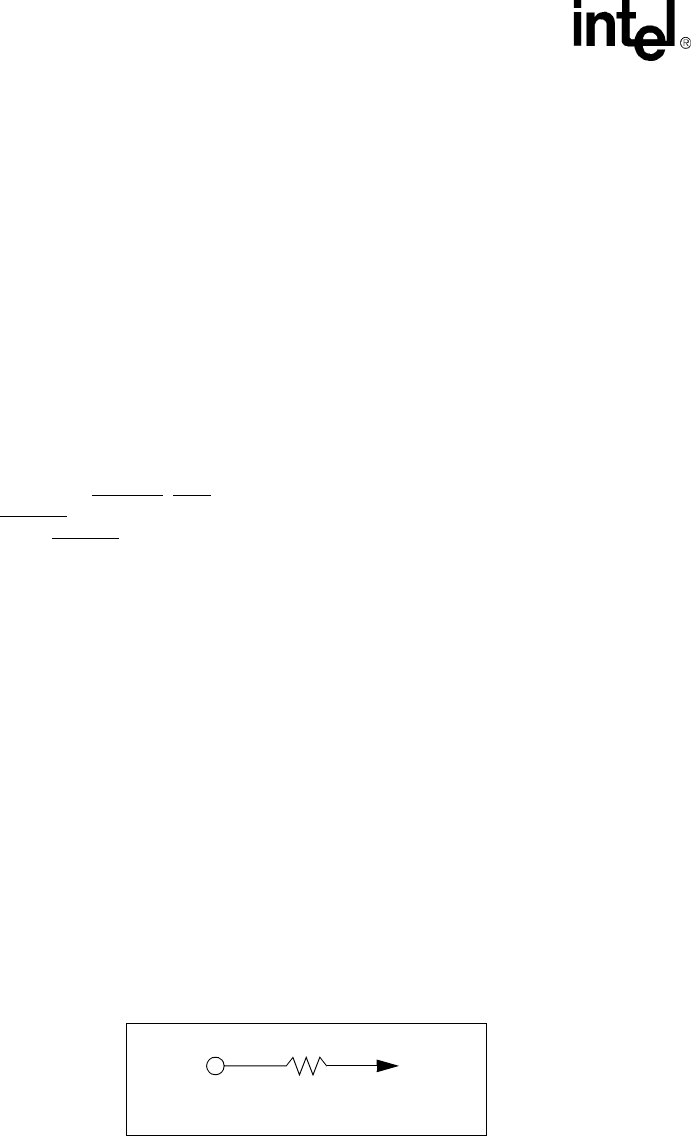
80960HA/HD/HT
38 Datasheet
4.3 Recommended Connections
Power and ground connections must be made to multiple VCC and VSS (GND) pins. Every
80960Hx-based circuit board should include power (VCC) and ground (VSS) planes for power
distribution. Every VCC pin must be connected to the power plane; every VSS pin must be
connected to the ground plane. Pins identified as “NC” —no connect pins—must not be connected
in the system.
Liberal decoupling capacitance should be placed near the 80960Hx. The processor may cause
transient power surges when its output buffers transition, particularly when connected to large
capacitive loads.
Low inductance capacitors and interconnects are recommended for best high-frequency electrical
performance. Inductance may be reduced by shortening the board traces between the processor and
decoupling capacitors as much as possible. Capacitors specifically designed for PGA packages
offer the lowest possible inductance.
For reliable operation, always connect unused inputs to an appropriate signal level. In particular,
any unused interrupt (XINT7:0, NMI) input should be connected to VCC through a pull-up resistor,
as should BTERM when not used. Pull-up resistors should be in the range of 20 KΩ for each pin
tied high. When READY or HOLD are not used, the unused input should be connected to ground.
N.C. pins must always remain unconnected.
4.4 VCC5 Pin Requirements (VDIFF)
In mixed-voltage systems that drive 80960Hx processor inputs in excess of 3.3 V, the VCC5 pin
must be connected to the system’s 5 V supply. To limit current flow into the VCC5 pin, there is a
limit to the voltage differential between the VCC5 pin and the other VCC pins. The voltage
differential between the 80960Hx VCC5 pin and its 3.3 V VCC pins should never exceed 2.25 V.
This limit applies to power-up, power-down, and steady-state operation. Table 21 outlines this
requirement.
Meeting this requirement ensures proper operation and ensures that the current draw into the VCC5
pin does not exceed the ICC5 specification.
When the voltage difference requirements cannot be met due to system design limitations, an
alternate solution may be employed. As shown in Figure 7, a minimum of 100Ω series resistor
may be used to limit the current into the VCC5 pin. This resistor ensures that current drawn by the
VCC5 pin does not exceed the maximum rating for this pin.
This resistor is not necessary in systems that may ensure the VDIFF specification.
In 3.3V-only systems and systems that drive 80960Hx pins from 3.3V logic, connect the VCC5
pin directly to the 3.3 V VCC plane.
Figure 7. VCC5 Current-Limiting Resistor
+5 V (±0.25 V) VCC5 Pin
100 Ω
(±5%, 0.5 W)

80960HA/HD/HT
Datasheet39
4.5VCCPLL Pin Requirements
When the voltage on the VCCPLL power supply pin exceeds the VCC pin voltage by 0.5V at any
time, including the power up and power down sequences, excessive currents may permanently
damage on-chip electrostatic discharge (ESD) protection diodes. The damage may accumulate over
multiple episodes.
Pragmatically, this problem only occurs when the VCCPLL and VCC pins are driven by separate
power supplies or voltage regulators. Applications that use one power supply for VCCPLL and
VCC are not typically at risk. Verify that your application does not allow the VCCPLL voltage to
exceed VCC by 0.5 V.
The VCCPL low-pass filter recommended in the Developer’s Manual does not promote this
problem.
Table 21. VDIFF Specification for Dual Power Supply Requirements (3.3 V, 5 V)
Sym Parameter MinMax UnitsNotes
VDIFF VCC5-VCC
Difference2.25 VVCC5 input should not exceed VCC by more than 2.25 V during
power-up and power-down, or during steady-state operation.

80960HA/HD/HT
40 Datasheet
4.6 D.C. Specifications
Table 22. 80960Hx D.C. Characteristics (Sheet 1 of 2)
Per the conditions described in Section 4.3, “Recommended Connections” on page 38.
Symbol ParameterMin TypMax UnitsNotes
VIL Input Low Voltage – 0.3+0.8V
VIH Input High Voltage 2.0VCC5 +0.3V
VOL Output Low Voltage
All outputs except FAIL
0.4
0.2VIOL = 3 mA
IOL = 100 µA
VOL Output Low Voltage FAIL pin 0.4 VIOL = 5 mA
VOH Output High Voltage 2.4
VCC – 0.2V
VIOH = –3 mA
IOH = –100 µA
ILI
Input Leakage Current
Non-Test Inputs
TDI, TMS, TRST and ONCE
-1 1
-110
µA
µA
0 ≤ VIN ≤ VCC
VIN = 0V
ILO
Output Leakage Current
Non-Test Outputs
TDO pin
1
5
µA
µA
0.45 ≤ VOUT ≤ VCC
0.45 ≤ VOUT ≤ VCC
ICC Active
(Power
Supply)
80960HA 25
33
40
80960HD 32
50
66
80
80960HT 60
75
579
765
927
631
985
1300
1578
1165
1455
mA 4, 5
ICC Active
(Thermal)
80960HA 25
33
40
80960HD 32
50
66
80
80960HT 60
75
392
518
628
413
645
851
1034
752
938
mA 4, 6
ICC Test
(Reset
Mode)
80960HA 25
33
40
80960HD 32
50
66
80
80960HT 60
75
330
436
528
382
595
785
955
702
878
mA 7, 8
ICC Test
(ONCE
mode) 25 mA7

80960HA/HD/HT
Datasheet41
ICC5
Current on
the VCC5
Pin
80960HA
80960HD
80960HT
200
200
200 µA 9
CIN
Input Capacitance for:
PQ4
PGA12
12 pF
pF
FC = 1 MHz10
COUTOutput Capacitance of each
output pin 12 pF FC = 1 MHz3, 10
CI/O I/O Pin Capacitance 12 pF FC = 1 MHz10
RPU
Internal Pull-Up Resistance
for ONCE, TMS, TDI and
TRST30 65 100 kΩ
NOTES:
1. ICC Maximum is measured at worst case frequency, VCC, and temperature, with device operating and
outputs loaded to the test conditions described in Section 4.7.1, “AC Test Conditions” on page 45.
2. ICC Typical is not tested.
3. Output Capacitance is the capacitive load of a floating output.
4. Measured with device operating and outputs loaded to the test conditions in Figure 8, “AC Test Load” on
page 45. Input signals rise to VCC and fall to VSS.
5. ICC Active (Power Supply) value is provided for selecting your system’s power supply. It is measured using
one of the worst case instruction mixes with VCC = 3.45 V. This parameter is characterized but not tested.
6. ICC Active (Thermal) value is provided for your system’s thermal management. Typical ICC is measured with
VCC = 3.3V and temperature = 25° C. This parameter is characterized but not tested.
7. ICC Test (Power modes) refers to the ICC values that are tested when the 80960HA/HD/HT is in Reset mode
or ONCE mode with VCC = 3.45 V.
8.Worst case is VCC = 3.45 V, 0 ° C.
9. ICC5 is tested at VCC = 3.0V, VCC5 = 5.25 V.
10.Pin capacitance is characterized, but not tested.
Table 22. 80960Hx D.C. Characteristics (Sheet 2 of 2)
Per the conditions described in Section 4.3, “Recommended Connections” on page 38.
SymbolParameterMin TypMax UnitsNotes

80960HA/HD/HT
42 Datasheet
4.7 A.C. Specifications
Table 23. 80960Hx A.C. Characteristics (Sheet 1 of 2)
Per conditions in Section 4.2, “Operating Conditions” on page 37 and Section 4.7.1, “AC Test Conditions” on page 45.
SymbolParameter MinMax UnitsNotes
Input Clock1, 7
TF
CLKIN Frequency80960HA
80960HD 80960HT
16
16
16
40
40
25
MHz
MHz
MHz
T
CLKIN Period
80960HA
80960HD 80960HT
25
25
40
62.5
62.5
62.5
ns
ns
ns
TCS CLKIN Period Stability-250 +250 ps11
TCH CLKIN High Time 8 ns11
TCL
CLKIN Low Time 80960HA
80960HD 80960HT
8
8
8
ns
ns
ns 11
TCR CLKIN Rise Time 0 4 ns 11
TCF CLKIN Fall Time 0 4 ns 11
Synchronous Outputs1, 2, 3, 6
TOV1, TOH1
Output Valid Delay and Output Hold for all
outputs except DT/R, BLAST and BREQ for
3.3V and 5 V inputs and I/Os.1.59.5ns
TOV2, TOH2
Output Valid Delay and Output Hold for DT/R
80960HA
80960HD
80960HT
T/2 + 1.5
3T/4 + 1.5
5T/6 + 1.5
T/2 + 9.5
3T/4 + 9.5
5T/6 + 9.5
ns
ns
ns
TOV3, TOH3Output Valid Delay and Output Hold for BLAST1.5 9 ns
TOV4, TOH4Output Valid Delay and Output Hold for BREQ 0.5 9 ns
TOV5, TOH5Output Valid Delay and Output Hold for A3:2 1.5 8.5
TOF Output Float for all outputs1.5 9 ns 11
Synchronous Inputs1, 7, 8, 9
TIS1Input Setup for all inputs except READY, BTERM,
HOLD, and BOFF 2.5ns
TIH1Input Hold for all inputs except READY, BTERM,
HOLD, and BOFF 2.5ns
NOTE:See Table 24, “AC Characteristics Notes” on page 44 for all notes related to AC specifications.
80960HA/HD/HT
Datasheet43
TIS2Input Setup for READY, BTERM, HOLD, and
BOFF 6ns
TIH2Input Hold for READY, BTERM, HOLD, and
BOFF 2.5ns
Relative Output Timings1, 2, 3, 6, 10
TAVSH1A31:2 Valid to ADS Rising T – 5T + 5ns10
TAVSH2BE3:0, W/R, SUP, D/C Valid to ADS Rising T – 5T + 5ns10
TAVEL1 A31:2 Valid to DEN Falling T – 5T + 5ns10
TAVEL2 BE3:0, W/R, SUP Valid to DEN Falling T – 5T + 5ns10
TNLQV WAIT Falling to Output Data Valid -5 5 ns10
TDVNH Output Data Valid to WAIT Rising -5 + N*T 5 + N*T ns 4, 10
TNLNH WAIT Falling to WAIT Rising -4 + N*T 4 + N*T ns 4, 10
TNHQXOutput Data Hold after WAIT Rising -5 +
(N+1)*T 5 + (N+1)*Tns5, 10
TEHTV DT/R Hold after DEN High T/2 – 5 Infinitens 10
TTVEL
DT/R Valid to DEN Falling
80960HA
80960HD
80960HT
T/2 – 4
T/4 – 4
T/6 – 4
ns
ns
ns
10
Relative Input Timings1, 7, 10
TIS7XINT7:0, NMI Input Setup 6 ns 9
TIH7XINT7:0, NMI Input Hold 2.5ns 9
TIS8RESET Input Setup 3 ns 8
TIH8RESET Input HoldT/4 + 1 ns 8
Table 23. 80960Hx A.C. Characteristics (Sheet 2 of 2)
Per conditions in Section 4.2, “Operating Conditions” on page 37 and Section 4.7.1, “AC Test Conditions” on page 45.
SymbolParameterMinMax UnitsNotes
NOTE:See Table 24, “AC Characteristics Notes” on page 44 for all notes related to AC specifications.

80960HA/HD/HT
44 Datasheet
Table 24. A.C. Characteristics Notes
NOTES:
1. See Section 4.8, “AC Timing Waveforms” on page 46 for waveforms and definitions.
2. See Figure 25, “Output Delay or Hold vs. Load Capacitance” on page 52 for capacitive derating information
for output delays and hold times.
3. See Figure 22, “Rise and Fall Time Derating at 85 °C and Minimum VCC” on page 51 for capacitive
derating information for rise and fall times.
4. Where N is the number of NRAD, NRDD, NWAD or NWDD wait states that are programmed in the Bus
Controller Region Table. WAIT never goes active when there are no wait states in an access.
5. N = Number of wait states inserted with READY.
6. These specifications are ensured by the processor.
7. These specifications must be met by the system for proper operation of the processor.
8. RESET is an asynchronous input that has no required setup and hold time for proper operation. However,
to ensure the device exits the reset mode synchronized to a particular clock edge, the rising edge of
RESET must meet setup and hold times to the rising edge of the CLKIN.
9. The interrupt pins are synchronized internally by the 80960Hx. They have no required setup or hold times
for proper operation. These pins are sampled by the interrupt controller every clock and must be active for
at least two consecutive CLKIN rising edges when asserting them asynchronously. To ensure recognition at
a particular clock edge, the setup and hold times shown must be met.
10.Relative Output timings are not tested.
11.Not tested.
12.The processor minimizes changes to the bus signals when transitioning from a bus cycle to an idle bus for
the following signals: A31:4, SUP, CT3:0, D/C, LOCK, W/R, BE3:0.
Table 25. 80960Hx Boundary Scan Test Signal Timings
Symbol ParameterMin Max UnitsNotes
TBSFTCK Frequency0 8 MHz
TBSCTCK Period 125 Infinitens
TBSCH TCK High Time 40 ns Measured at 1.5V†
TBSCL TCK Low Time 40 ns Measured at 1.5V†
TBSCR TCK Rise Time 8 ns0.8V to 2.0 V†
TBSCF TCK Fall Time 8 ns2.0V to 0.8V†
TBSIS1Input Setup to TCK —
TDI, TMS8ns
TBSIH1Input Hold from TCK —
TDI, TMS 10 ns
TBSOV1TDO Valid Delay3 30 ns
TBSOF1TDO Float Delay 36 ns†
TBSOV2All Outputs (Non-Test)
Valid Delay 330ns
Relative to TCK
TBSOF2All Outputs (Non-Test)
Float Delay 36 ns Relative to TCK†
TBSIS2Input Setup to TCK - All
Inputs (Non-Test)8ns
TBSIH2Input Hold from TCK - All
Inputs (Non-Test)10 ns
†Not tested.
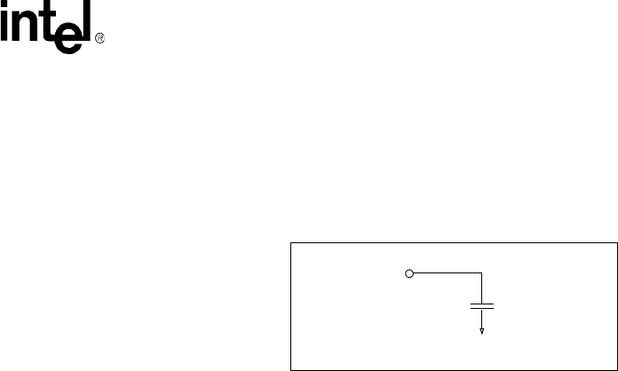
80960HA/HD/HT
Datasheet45
4.7.1 A.C. Test Conditions
A.C. values are derived using the 50 pF load shown in Figure 8. Figure 25, “Output Delay or Hold vs.
Load Capacitance” on page52, shows how timings vary with load capacitance. Input waveforms
(except for CLKIN) are assumed to have a rise and fall time of ≤2ns from 0.8V to 2.0V.
Figure 8. A.C. Test Load
Output Pin
CL = 50 pF for all signals
CL
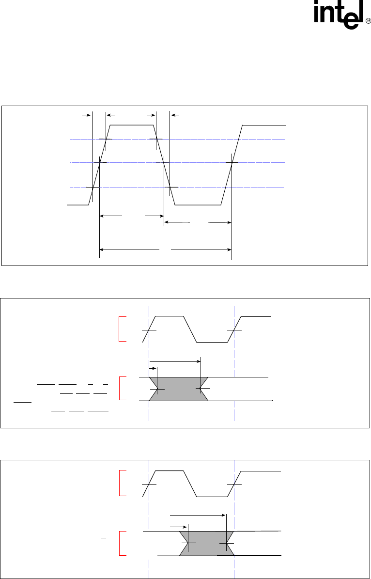
80960HA/HD/HT
46 Datasheet
4.8 A.C. Timing Waveforms
Figure 9. CLKIN Waveform
Figure 10. Output Delay Waveform
Figure 11. Output Delay Waveform
2.0 V
1.5 V
0.8 V
TCF
TCH TCL
T
TCR
CLKIN
Outputs:
1.5 V
1.5 V
TOV1
MinMax
TOH1
1.5 V
1.5 V
A31:2, D31:0 write only,
DP3:0 write only
PCHK, BE3:0, W/R, D/C,
SUP, ADS, DEN,
LOCK, HOLDA, BREQ, BSTALL,
CT3:0, FAIL, WAIT, BLAST
CLKIN 1.5V
1.5V
DT/R
MinMax
TOH2
1.5 V1.5 V
TOV2
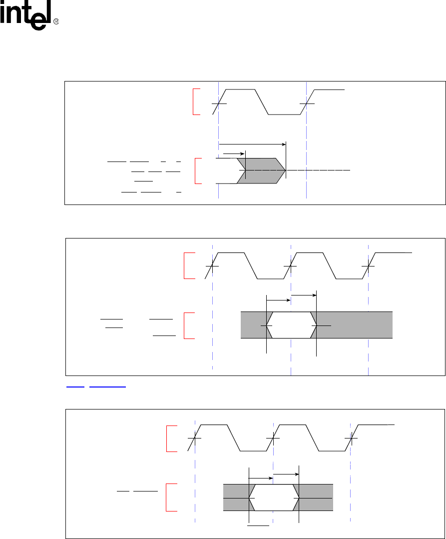
80960HA/HD/HT
Datasheet47
Figure 12. Output Float Waveform
Figure 13. Input Setup and Hold Waveform
Figure 14. NMI, XINT7:0 Input Setup and Hold Waveform
MinMax
TOF
Outputs:
A31:2, D31:0 write only,
DP3:0 write only
PCHK, BE3:0, W/R, D/C,
SUP, ADS, DEN,
LOCK, HOLDA,
CT3:0, WAIT, BLAST, DT/R
CLKIN 1.5V
1.5V
CLKIN
Inputs:
1.5 V1.5 V1.5 V
Valid
TIS TIH
READY, HOLD, BTERM,
BOFF, D31:0 on reads,
MinMin
DP3:0 on reads, RESET
CLKIN 1.5 V1.5 V1.5 V
Valid
TIS TIH
NMI, XINT7:0
MinMin
1.5 V
1.5 V
ABA
NOTE:A and B edges are established by de-assertion of RESET. See Figure 29, “Cold Reset Waveform” on page 54.
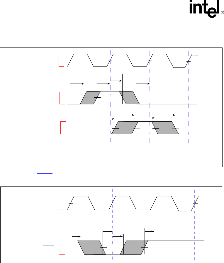
80960HA/HD/HT
48 Datasheet
Figure 15. Hold Acknowledge Timings
Figure 16. Bus Backoff (BOFF) Timings
CLKIN 1.5 V
1.5 V 1.5 V
HOLD
TIS
TIH
1.5 V
TIH TIS
HOLDA
TOV1
Min
MinMin
Min
TOV1 Max
Min
Max
Min
TOH1TOH1
TOV TOH — OUTPUT DELAY - The maximum output delay is referred to as the Output Valid Delay (TOV).
The minimum output delay is referred to as the Output Hold (TOH).
TIS TIH — INPUT SETUP AND HOLD - The input setup and hold requirements specify the sampling window
during which synchronous inputs must be stable for correct processor operation.
1.5 V
1.5 V
1.5 V 1.5 V
1.5 V
CLKIN 1.5V
1.5V 1.5V
BOFF
TIS
TIH TIH
TIS
1.5V1.5 V1.5 V
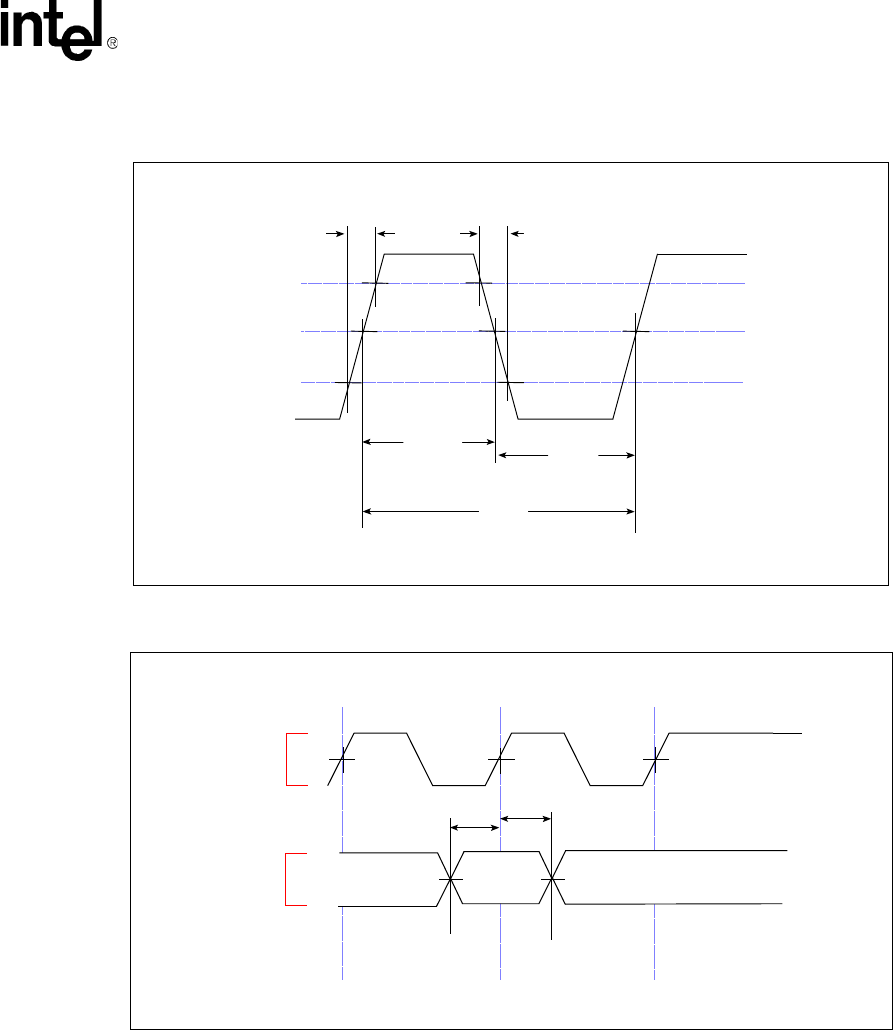
80960HA/HD/HT
Datasheet49
Figure 17. TCK Waveform
Figure 18. Input Setup and Hold Waveforms for TBSIS1 and TBSIH1
2.0V
1.5V
0.8V
TBSCF
TBSCH TBSCL
TBSC
TBSCR
TCLK
Inputs:
TMS
1.5 V1.5 V1.5 V
TDI1.5 V 1.5 V
Valid
TBSIS1 TBSIH1
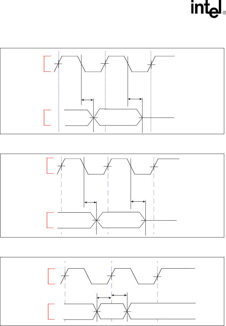
80960HA/HD/HT
50 Datasheet
Figure 19. Output Delay and Output Float for TBSOV1 and TBSOF1
Figure 20. Output Delay and Output Float Waveform for TBSOV2 and TBSOF2
Figure 21. Input Setup and Hold Waveform for TBSIS2 and TBSIH2
TCK1.5 V
1.5 V
1.5 V
1.5 V
TBSOV1
TDOValid
TBSOF1
TCK1.5 V
1.5 V
1.5 V
1.5 V
TBSOV2
Non-TestValid
TBSOF2
Outputs
TCK
Non-Test
1.5 V
1.5 V
1.5 V
1.5 V 1.5 V
Valid
TBSIS2 TBSIH2
Inputs
80960HA/HD/HT
Datasheet51
Figure 22. Rise and Fall Time Derating at 85 ° C and Minimum VCC
Figure 23. ICC Active (Power Supply) vs. Frequency
50pF 100pF 150pF
Time (ns)
CL (pF)
5
4
3
2
1
2.0 to 0.8V
0.8 to 2.0V
0
ICC Active (Power Supply) (mA)
CLKIN Frequency (MHz)
200
1800
1600
1400
1200
1000
800
600
400
10 20 30 40
HA
HT
HD
0
80960HA/HD/HT
52 Datasheet
Figure 24. ICC Active (Thermal) vs. Frequency
Figure 25. Output Delay or Hold vs. Load Capacitance
ICC Active (Thermal) (mA)
CLKIN Frequency (MHz)
200
1400
1200
1000
800
600
400
10 20 30 40
HA
HT
HD
50 100 150
CL (pF)
nom + 10
nom + 5
nom
Output Valid Delays (ns) @ 1.5 V
5.5 V Input Signals
3.3 V Input Signals
80960HA/HD/HT
Datasheet53
Figure 26. Output Delay vs. Temperature
Figure 27. Output Hold Times vs. Temperature
Figure 28. Output Delay vs. VCC
nom - 0.0
nom - 0.4
nom - 0.5
Output Valid Delays (ns) @ 1.5 V
nom - 0.3
nom - 0.2
nom - 0.1
Processor Case Temperature (°C)
85°C0° C
nom + 0.5
nom + 0.1
nom + 0
Output Hold Times (ns) @ 1.5 V
nom + 0.2
nom + 0.3
nom + 0.4
Processor Case Temperature (°C)
85°C0° C
nom + 0.5
-nom + 0.3
-nom + 0.5
Output Valid or Hold Delays (ns) @ 1.5 V
-nom + 0.1
nom + 0.1
nom + 0.3
VCC (volts)
3.15 3.45
80960HA/HD/HT
54 Datasheet
5.0 Bus Waveforms
Figure 29. Cold Reset Waveform
CLKIN
CT3:0, ADS,
W/R, DT/R,
D31:0,
STEST
RESET
VCC, VCC5,
LOCK, WAIT,
DEN, BLAST
BREQ, FAIL,
DP3:0
∼
∼
∼
∼
∼
∼
∼
∼
∼
∼
∼
∼
∼
∼∼
∼∼
∼∼
∼∼
∼∼
∼∼
∼∼
∼
Invalid
Valid
∼
∼
∼
∼
∼
∼
∼
∼
∼
∼
∼
∼
∼
∼
∼
∼
Inputs
Tsetup
1CLKIN Thold
1CLKIN
∼
∼
∼
∼
∼
∼
∼
∼
∼
∼
∼
∼
∼
∼
∼
∼
∼
∼
∼
∼∼
∼
∼
∼
∼
∼
∼
∼
A31:2, SUP
D/C, BE3:0
BABA
~
~
∼
∼
∼
∼
ONCE
NOTE:VCC stable: As specified in Table21, “VDIFF Specification for Dual Power Supply Requirements (3.3V, 5 V)” on page 39
RESET high to First Bus Activity,
HA=67, HD=34, HT=23
CLKIN periods
CLKIN and VCC Stable to RESET high,
minimum 10,000 CLKIN periods
for PLL stabilization.
BSTALL
80960HA/HD/HT
Datasheet55
Figure 30. Warm Reset Waveform
∼
∼∼
∼
∼
∼∼
∼
Maximum RESET Low to RESET State
16 CLKIN Periods1 CLKIN
∼
∼∼
∼
∼
∼∼
∼∼
∼
∼
∼
∼
∼
CLKIN
ADS,
DT/R
SUP,
D31:0,
STEST
RESET
LOCK, WAIT,
DEN, BLAST,
A31:2,
D/C, BE3:0
DP3:0
Valid
∼
∼∼
∼
Thold
Tsetup
1 CLKIN
∼
∼
∼
∼
W/R, BREQ, FAIL,
∼
∼
∼
∼
BSTALL
Minimum RESET Low Time
16 CLKIN Periods
RESET High to First Bus Activity,
HA=67, HD=34, HT=23
CLKIN Periods
80960HA/HD/HT
56 Datasheet
Figure 31. Entering ONCE Mode
CLKIN
ADS, BE3:0, A31:2,
RESET
ONCE
∼
∼
∼
∼
∼
∼
∼
∼∼
∼∼
∼
∼
∼
∼
∼
∼
∼
∼
∼
∼
∼
∼
∼
CLKIN and VCC Stable and RESET low and ONCE low to
RESET high, minimum 10,000 CLKIN Periods.
D31:0, LOCK, WAIT,
BLAST,W/R, D/C, DEN,
DT/R, HOLDA,
CT3:0, BSTALL, DP3:0,
PCHK
BLAST, FAIL, SUP,BREQ,
VCC, VCC5
∼
∼
∼
∼∼
∼
∼
∼
ONCE mode is entered within 1 CLKIN
period after ONCE becomes low while
RESET is low.
∼
∼
∼
∼
∼
∼
∼
∼
CLKIN may neither float nor remain idle.
It must continue to run.
NOTES:
1. ONCE mode may be entered prior to the rising edge of RESET: ONCE input is not latched until the rising
edge of RESET.
2. The ONCE input may be removed after the processor enters ONCE mode.
80960HA/HD/HT
Datasheet57
Figure 32. Non-Burst, Non-Pipelined Requests without Wait States
In
ADS
A31:2, SUP,
D/C,
LOCK, CT3:0
W/R
BLAST
DT/R
DEN
WAIT
D31:0,
CLKIN
AD ADAD
In
Valid Valid Valid
BurstBus
WidthOdd ParityNXDANWDDNWADNRDD
29 28 2124 23-22 20 12-819-16 15-14 7-6 4-0
Disabled
0OFF
00
0000
X
xx X
xEnabled
10
00 0
00000 0
00
Disabled
00
00000
Out
Function
Bit
Value
BE3:0,
DP3:0
PCHK
External
Ready
Control
Pipe-
Lining Parity EnableNRAD
NOTE:Bits 31-30, 27-25, 13, and 5 are reserved.
PMCON
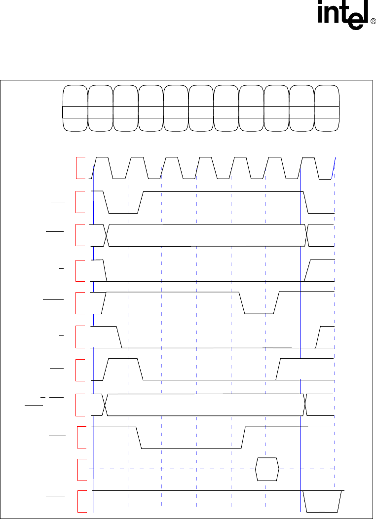
80960HA/HD/HT
58 Datasheet
Figure 33. Non-Burst, Non-Pipelined Read Request with Wait States
ADS
A31:2, BE3:0
W/R
BLAST
DT/R
DEN
WAIT
D31:0,
CLKIN
A321D1
In
Valid
Valid
A
DP3:0
PCHK
NOTE:Bits 31-30, 27-25, 13, and 5 are reserved.
BurstBus
WidthOdd ParityNXDA NWDD NWADNRDD
29 28 2124 23-22 20 12-819-16 15-14 7-6 4-0
Disabled
0OFF
01
0001
X
xx X
xEnabled
1X
xx X
xxxxx X
xx
Disabled
03
00011
Function
Bit
Value
External
Ready
Control
Pipe-
Lining ParityEnableNRAD
PMCON
D/C, SUP,
LOCK, CT3:0
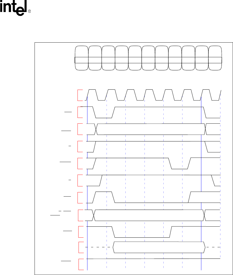
80960HA/HD/HT
Datasheet59
Figure 34. Non-Burst, Non-Pipelined Write Request with Wait States
ADS
A31:2,
W/R
BLAST
DT/R
DEN
WAIT
D31:0,
CLKIN
A3 21 D1
Out
A
Valid
Valid
BE3:0
DP3:0
PCHK
BurstBus
WidthOdd ParityNXDANWDDNWADNRDD
29 28 2124 23-22 20 12-819-16 15-147-6 4-0
Disabled
0OFF
01
0001
X
xx X
xEnabled
1X
xxxxx 3
00011 X
xx
Disabled
0X
xxxxx
Function
Bit
Value
External
Ready
Control
Pipe-
Lining Parity EnableNRAD
NOTE:Bits 31-30, 27-25, 13, and 5 are reserved.
PMCON
D/C, SUP,
LOCK, CT3:0
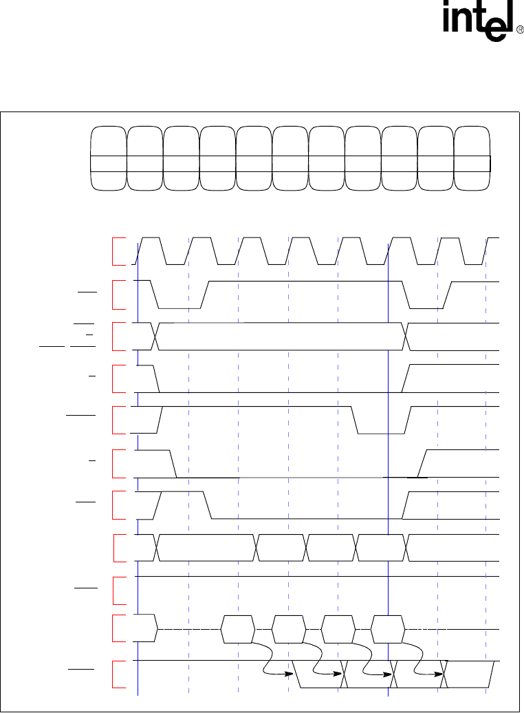
80960HA/HD/HT
60 Datasheet
Figure 35. Burst, Non-Pipelined Read Request without Wait States, 32-Bit Bus
In0
ADS
A31:4, SUP,
CT3:0,D/C,
BE3:0, LOCK
W/R
BLAST
DT/R
DEN
A3:2
WAIT
D31:0,
CLKIN
AD DD DA
In3In2In1
Valid
00 01 10 11
DP3:0
PCHK
BurstBus
WidthOdd ParityNXDA NWDD NWADNRDD
29 28 2124 23-22 20 12-819-16 15-14 7-6 4-0
Enabled
1OFF
00
0000
32-Bit
10 X
xEnabled
1X
xx X
xxxxx 0
00
Disabled
00
00000
Function
Bit
Value
External
Ready
Control
Pipe-
Lining Parity EnableNRAD
NOTE:Bits 31-30, 27-25, 13, and 5 are reserved.
PMCON
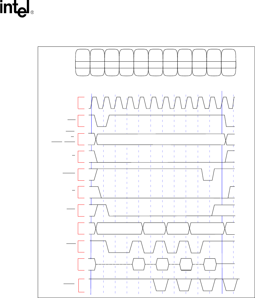
80960HA/HD/HT
Datasheet61
Figure 36. Burst, Non-Pipelined Read Request with Wait States, 32-Bit Bus
ADS
A31:4, SUP,
CT3:0, D/C,
BE3:0, LOCK
W/R
BLAST
DT/R
DEN
A3:2
WAIT
D31:0,
CLKIN
A21D1D1D1D1A
In1In2 In3
In0
Valid
00 1101 10
DP3:0
PCHK
BurstBus
WidthOdd ParityNXDA NWDD NWADNRDD
29 28 2124 23-22 20 12-819-16 15-14 7-6 4-0
Enabled
1OFF
01
0001
32-Bit
10 X
xEnabled
1X
xx X
xxxxx 1
01
Disabled
02
00010
Function
Bit
Value
External
Ready
Control
Pipe-
Lining Parity EnableNRAD
NOTE:Bits 31-30, 27-25, 13, and 5 are reserved.
PMCON
80960HA/HD/HT
62 Datasheet
Figure 37. Burst, Non-Pipelined Write Request without Wait States, 32-Bit Bus
ADS
A31:4, SUP,
CT3:0, D/C,
BE3:0, LOCK
W/R
BLAST
DT/R
DEN
A3:2
WAIT
D31:0,
CLKIN
AD DDDA
00 01 10 11
Out0 Out3
Out2
DP3:0
PCHK
Out1
BurstBus
WidthOdd ParityNXDA NWDD NWADNRDD
29 28 2124 23-22 20 12-819-16 15-14 7-6 4-0
Enabled
1OFF
00
0000
32-Bit
10 X
xEnabled
10
00 0
00000 X
xx
Disabled
0X
xxxxx
Function
Bit
Value
External
Ready
Control
Pipe-
Lining ParityEnableNRAD
NOTE:Bits 31-30, 27-25, 13, and 5 are reserved.
PMCON
Valid
80960HA/HD/HT
Datasheet63
Figure 38. Burst, Non-Pipelined Write Request with Wait States, 32-Bit Bus
ADS
A31:4, SUP,
CT3:0, D/C,
BE3:0, LOCK
W/R
BLAST
DT/R
DEN
A3:2
WAIT
D31:0,
CLKIN
A21D1D1D1D1A
Out0
Valid
00 1101 10
Out1 Out2 Out3
DP3:0
PCHK
BurstBus
WidthOdd ParityNXDANWDDNWADNRDD
29 28 2124 23-22 20 12-819-16 15-147-6 4-0
Enabled
1OFF32-bit
01
0001
10 X
xEnabled
11
01 2
00010 X
xx
Disabled
0X
xxxxx
Function
Bit
Value
External
Ready
Control
Pipe-
Lining Parity EnableNRAD
NOTE:Bits 31-30, 27-25, 13, and 5 are reserved.
PMCON
80960HA/HD/HT
64 Datasheet
Figure 39. Burst, Non-Pipelined Read Request with Wait States, 16-Bit Bus
ADS
SUP, CT3:0,
W/R
BLAST
DT/R
DEN
A3:2
WAIT
D31:0,
CLKIN
A21D1D1D1D1A
Valid
A3:2 = 00 or 10 A3:2 = 01 or 11
D15:0
A1=0
D15:0
A1=1 D15:0
A1=0D15:0
A1=1
D/C, LOCK,
A31:4, BE3/BHE,
BE1/A1
BE0/BLE
DP3:0
PCHK
BurstBus
WidthOdd ParityNXDANWDD NWADNRDD
29 28 2124 23-22 20 12-819-16 15-14 7-6 4-0
Enabled
1OFF
01
0001
16-BitX
xEnabled
1X
xx X
xxxxx 1
01
Disabled
02
00010
Function
Bit
Value
External
Ready
Control
Pipe-
Lining Parity EnableNRAD
NOTE:Bits 31-30, 27-25, 13, and 5 are reserved.
01
PMCON
80960HA/HD/HT
Datasheet65
Figure 40. Burst, Non-Pipelined Read Request with Wait States, 8-Bit Bus
ADS
SUP, CT3:0,
W/R
BLAST
DT/R
DEN
A3:2
WAIT
D31:0,
CLKIN
A21D1D1D1D1A
Valid
A3:2 = 00, 01, 10 or 11
D7:0
Byte 0
D7:0
Byte 1 D7:0
Byte 2
D7:0
Byte 3
D/C, LOCK,
A31:4
BE1/A1, A1:0 = 00 A1:0 = 01 A1:0 = 10 A1:0 =11
BE0/A0
DP3:0
PCHK
BurstBus
WidthOdd ParityNXDA NWDDNWAD NRDD
29 28 2124 23-22 20 12-819-16 15-14 7-6 4-0
Enabled
1OFF
01
0001
8-BitX
xEnabled
1X
xx X
xxxxx 1
01
Disabled
02
00010
Function
Bit
Value
External
Ready
Control
Pipe-
Lining Parity EnableNRAD
NOTE:Bits 31-30, 27-25, 13, and 5 are reserved.
00
PMCON
80960HA/HD/HT
66 Datasheet
Figure 41. Non-Burst, Pipelined Read Request without Wait States, 32-Bit Bus
ADS
A31:4, SUP,
CT3:0, D/C,
LOCK
BLAST
WAIT
D31:0,
CLKIN
IN
DIN
D’IN
D’’ IN
D’’’ IN
D’’’’
AA’
DA’’
D’A’’’
D’’
A’’’’
D’’’ D’’’’
Valid Valid Valid ValidValid Invalid
DT/R
DEN
A3:2
BE3:0Valid Valid Valid Valid Valid Invalid
W/R
DP3:0
PCHK
1.Non-pipelined request concludes, pipelined reads begin.
2. Pipelined reads conclude, non-pipelined requests begin.
12
BurstBus
WidthOdd ParityNXDA NWDDNWAD NRDD
29 28 2124 23-22 20 12-819-16 15-14 7-6 4-0
Disabled
0ON
1X
xxxx
32-BitX
xEnabled
1X
xx X
xxxxx X
xx
X
x0
00000
Function
Bit
Value
External
Ready
Control
Pipe-
Lining Parity EnableNRAD
NOTE:Bits 31-30, 27-25, 13, and 5 are reserved.
10
Invalid
PMCON
80960HA/HD/HT
Datasheet67
Figure 42. Non-Burst, Pipelined Read Request with Wait States, 32-Bit Bus
ADS
A31:4, SUP,
CT3:0, D/C,
W/R
BLAST
DT/R
DEN
A3:2
WAIT
D31:0,
CLKIN
BE3:0
A1 A’
D1D’
IN
D’
Valid Valid Invalid
IN
D
LOCK
Valid Valid Invalid
DP3:0
1. Non-pipelined request concludes, pipelined reads begin
2. Pipelined reads conclude, non-pipelined requests begin
PCHK
2
1
BurstBus
WidthOdd ParityNXDA NWDDNWAD NRDD
29 28 2124 23-22 20 12-819-16 15-14 7-64-0
Disabled
0ON
1X
xxxx
32-BitX
xEnabled
1X
xx X
xxxxx X
xx
X
x1
00001
Function
Bit
Value
External
Ready
Control
Pipe-
Lining Parity EnableNRAD
NOTE:Bits 31-30, 27-25, 13, and 5 are reserved.
10
Invalid
PMCON
80960HA/HD/HT
68 Datasheet
Figure 43. Burst, Pipelined Read Request without Wait States, 32-Bit Bus
ADS
A31:4, SUP,
CT3:0, D/C,
BE3:0, LOCK
W/R
BLAST
DT/R
DEN
A3:2
WAIT
D31:0,
CLKIN
ADDDA’D’D’
Valid Valid
In-
ValidValid01 10 1100
IN
DIN
DIN
DIN
DIN
DIN
D
Valid
D
In-
Valid
DP3:0
PCHK
12
BurstBus
WidthOdd ParityNXDA NWDDNWAD NRDD
29 28 2124 23-22 20 12-819-16 15-14 7-6 4-0
Enabled
1ON
1X
xxxx
32-BitX
xEnabled
1X
xx X
xxxxx 0
00
X
x0
00000
Function
Bit
Value
External
Ready
Control
Pipe-
Lining Parity EnableNRAD
NOTE:Bits 31-30, 27-25, 13, and 5 are reserved.
10
PMCON
1. Non-pipelined request concludes, pipelined reads begin
2. Pipelined reads conclude, non-pipelined requests begin
80960HA/HD/HT
Datasheet69
Figure 44. Burst, Pipelined Read Request with Wait States, 32-Bit Bus
ADS
A31:4, SUP,
CT3:0, D/C,
BE3:0, LOCK
W/R
A3:2
D31:0,
WAIT
BLAST
DT/R
DEN
CLKIN
IN
DIN
DIN
DIN
DIN
D’
A21 D1D1D1A’21
Valid
DD’
Valid In-
valid
In-
valid
00 01 10 11 ValidIn-
valid
DP3:0
PCHK
1. Non-pipelined request concludes, pipelined reads begin.
2. Pipelined reads conclude, non-pipelined requests begin.
2
1
NOTE:Bits 31-30, 27-25, 13, and 5 are reserved.
BurstBus
WidthOdd ParityNXDANWDD NWADNRDD
29 28 2124 23-22 20 12-819-16 15-14 7-6 4-0
Enabled
1ON
1X
xxxx
32-BitX
xEnabled
1X
xx X
xxxxx 1
01
X
x2
00010
Function
Bit
Value
External
Ready
Control
Pipe-
Lining Parity EnableNRAD
10
PMCON
80960HA/HD/HT
70 Datasheet
Figure 45. Burst, Pipelined Read Request with Wait States, 8-Bit Bus
ADS
A31:4, SUP,
CT3:0, D/C,
LOCK
W/R
A3:2
BE1/A1,
WAIT
BLAST
DT/R
DEN
CLKIN
D7:0
Byte 0 D7:0
Byte 1 D7:0
Byte 2 D7:0
Byte 3 D7:0
D’
A21D1D1D1A’21
DD’
In-
valid
Valid In-
valid
BE0/A0
D31:0,
A3:2 = 00, 01, 10, or 11Valid In-
valid
A1:0 = 00A1:0 = 01 A1:0 = 10A1:0 = 11
Valid Valid In-
valid
DP3:0
1.Non-pipelined request concludes, pipelined reads begin
2.Pipelined reads conclude, non-pipelined requests begin
PCHK
2
BurstBus
WidthOdd ParityNXDANWDD NWADNRDD
29 28 2124 23-22 20 12-819-16 15-14 7-6 4-0
Enabled
1ON
1X
xxxx
8-BitX
xEnabled
1X
xx X
xxxxx 1
01
X
x2
00010
Function
Bit
Value
External
Ready
Control
Pipe-
Lining Parity EnableNRAD
00
NOTE:Bits 31-30, 27-25, 13, and 5 are reserved.
PMCON
1
80960HA/HD/HT
Datasheet71
Figure 46. Burst, Pipelined Read Request with Wait States, 16-Bit Bus
ADS
A31:4, SUP,
CT3:0, D/C,
BE0/BLC,
W/R
A3:2
BE1/A1
WAIT
BLAST
DT/R
DEN
CLKIN
D15:0
A1=0 D15:0
A1=1 D15:0
A1=0 D15:0
A1=1 D15:0
D’
A21D1D1D1A’21
Valid
DD’
Valid In-
valid
In-
valid
A3:2 = 00 or 10 A3:2 = 01 or 11ValidIn-
valid
Valid In-
valid
BE3/BHE,
D31:0,
LOCK
DP3:0
PCHK
2
1
BurstBus
WidthOdd ParityNXDA NWDDNWADNRDD
29 28 2124 23-22 20 12-819-16 15-147-6 4-0
Enabled
1ON
1X
xxxx
16-BitX
xEnabled
1X
xx X
xxxxx 1
01
X
x2
00010
Function
Bit
Value
External
Ready
Control
Pipe-
Lining Parity EnableNRAD
NOTE:Bits 31-30, 27-25, 13, and 5 are reserved.
01
PMCON
1. Non-pipelined request concludes, pipelined reads begin
2. Pipelined reads conclude, non-pipelined requests begin
80960HA/HD/HT
72 Datasheet
Figure 47. Using External READY
CLKIN
ADS
A31:4, SUP,
DT/R
DEN
READY
W/R
CT3:0, D/C,
BLAST
BTERM
A3:2
WAIT
D31:0,
BE3:0, LOCK
D0 D1 D2D3 D0 D1 D2 D3
00 01 10 11 00 01 10 11
ValidValid
Quad-Word Read Request
NRAD = 0, NRDD = 0, NXDA = 0
Ready Enabled
Quad-Word Write Request
NWAD = 1, NWDD = 0, NWDA = 0
Ready Enabled
DP3:0
PCHK
A 1 D D D D1A 2D1D1D1D
NOTE: Pipelining must be disabled to use READY.
80960HA/HD/HT
Datasheet73
Figure 48. Terminating a Burst with BTERM
CLKIN
ADS
A31:4, SUP,
DT/R
DEN
READY
W/R
CT3:0, D/C,
BLAST
BTERM
A3:2
WAIT
D31:0,
BE3:0, LOCK
D0 D1 D2 D3
Valid
Quad-Word Read Request
NRAD = 0, NRDD = 0, NRDA = 0
Ready Enabled
00 01 10 11
Note: READY adds memory access time to data transfers, whether or not the
bus access is a burst access. BTERM interrupts a bus access, whether or not
the bus access has more data transfers pending. Either the READY signal or
the BTERM signal terminates a bus access when the signal is asserted during
the last (or only) data transfer of the bus access.
See Note
DP3:0
PCHK
D1 AD1DAA1D1
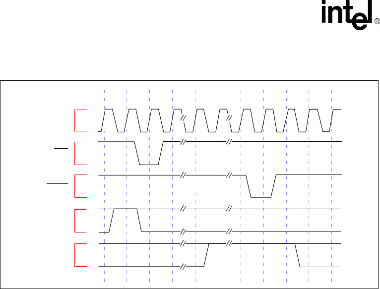
80960HA/HD/HT
74 Datasheet
The processor may stall (BSTALL asserted) even with an empty bus queue (BREQ deasserted).
Depending on the instruction stream and memory wait states, the two signals may be separated by
several CLKIN cycles.
Bus arbitration logic that logically ‘ANDs’ BSTALL and BREQ will not correctly grant the bus to
the processor in all stall cases, potentially degrading processor performance.
Do not logically ‘AND’ BSTALL and BREQ together in arbitration logic. Instead, the simplest bus
arbitration should logically “OR” BSTALL and BREQ to determine the processor’s bus ownership
requirements.
More sophisticated arbitration should recognize the priority nature of these two signals. Using a
traffic light analogy, BREQ is a ‘yellow light’ warning of a possible processor stall and BSTALL is
a ‘red light’ indicating a stall in progress.
Figure 49. BREQ and BSTALL Operation
CLKIN
ADS
BLAST
BREQ
BSTALL
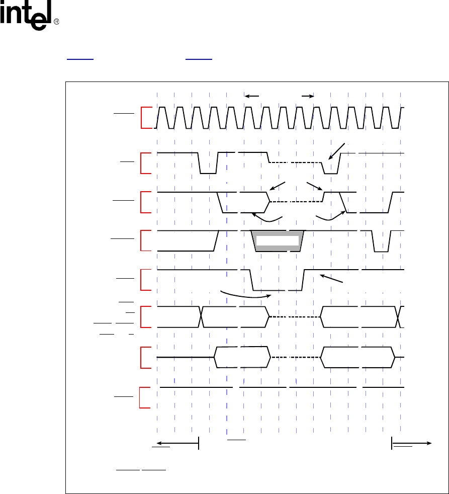
80960HA/HD/HT
Datasheet75
Figure 50. BOFF Functional Timing. BOFF occurs during a burst or non-burst data cycle.
ADS
BLAST
READY
BOFF
A31:2, SUP,
DP3:0 & D31:0,
BOFF may not
be asserted
BOFF may not
be asserted
BOFF may be asserted to suspend request
Begin Request End Request
Suspend Request
Non-Burst
CT3:0, D/C,
BE3:0, WAIT,
DEN, DT/R
(WRITES)
Burst
Resume Request
∼
∼
∼
∼
∼
∼
∼
∼
∼
∼
∼
∼
∼
∼
∼
∼
∼
∼
∼
∼
∼
∼
∼
∼
∼
∼
∼
∼
∼
∼
∼
∼
∼
∼
∼
∼
∼
∼
∼
∼
Note: READY/BTERM must be enabled; NRAD, NRDD, NWAD, NWDD= 0
∼
∼
∼
∼
ValidValid
CLKIN
PCHK
∼
∼
∼
∼
∼
∼∼
∼∼
∼∼
∼
A D A
May Change
BOFF Mode
Regenerate ADS
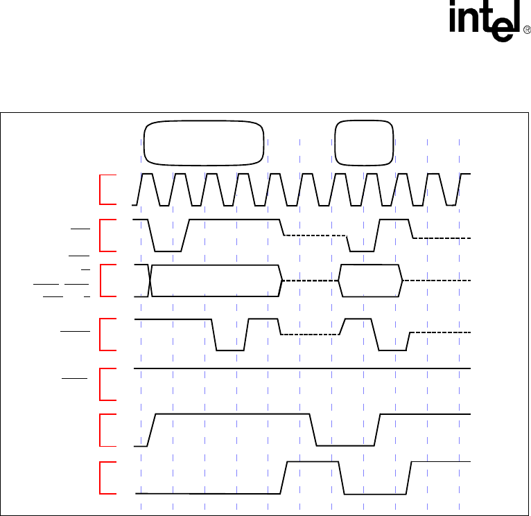
80960HA/HD/HT
76 Datasheet
Figure 51. HOLD Functional Timing
Word Read Request
NRAD=1, NXDA=1
Word Read
Request
NRAD=0,
NXDA=0
Hold StateHold State
CLKIN
ADS
A31:2, SUP,
CT3:0, D/C,
BE3:0, WAIT,
DEN, DT/R
BLAST
HOLD
HOLDA
ValidValid
LOCK
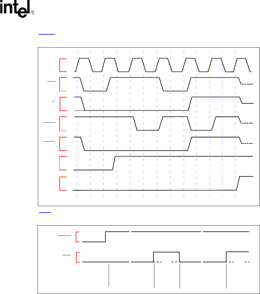
80960HA/HD/HT
Datasheet77
Figure 52. LOCK Delays HOLDA Timing
Figure 53. FAIL Functional Timing
CLKIN
ADS
BLAST
HOLD
HOLDA
LOCK
W/R
RESET
FAIL
257,517 Cycles30 Cycles 113 Cycles
(Bus Test)
Pass
(Internal Self-Test)
Pass
~
~
~
~
~
~
~
~
Fail Fail
80960HA:
80960HD: 128,761 Cycles 15 Cycles 94 Cycles
80960HT: 85,840 Cycles10 Cycles 90 Cycles
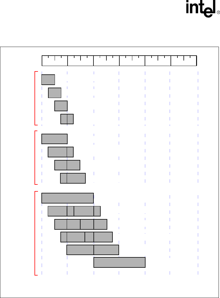
80960HA/HD/HT
78 Datasheet
Figure 54. A Summary of Aligned and Unaligned Transfers for 32-Bit Regions
04 812162024
01 234 56
One Double-Word
Short-Word
Load/Store
Word
Load/Store
Double-Word
Load/Store
Short Requests (Unaligned)
Short Request (Aligned)
Short Request (Aligned)
Byte, Byte Requests
Word Request (Aligned)
Trey, Byte, Requests
Short, Short Requests
Byte, Trey, Requests
Byte Offset
Word Offset
One Double-Word Burst (Aligned)
Trey, Byte, Trey, Byte, Requests
Short, Short, Short, Short Requests
Byte, Trey, Byte, Trey, Requests
Word, Word Requests
Request (Aligned)
NOTES:
1.All requests that are less than a word in size and are cacheable will be promoted to a word to be cached. This causes
adjacent requests to occur for full words to the same address.
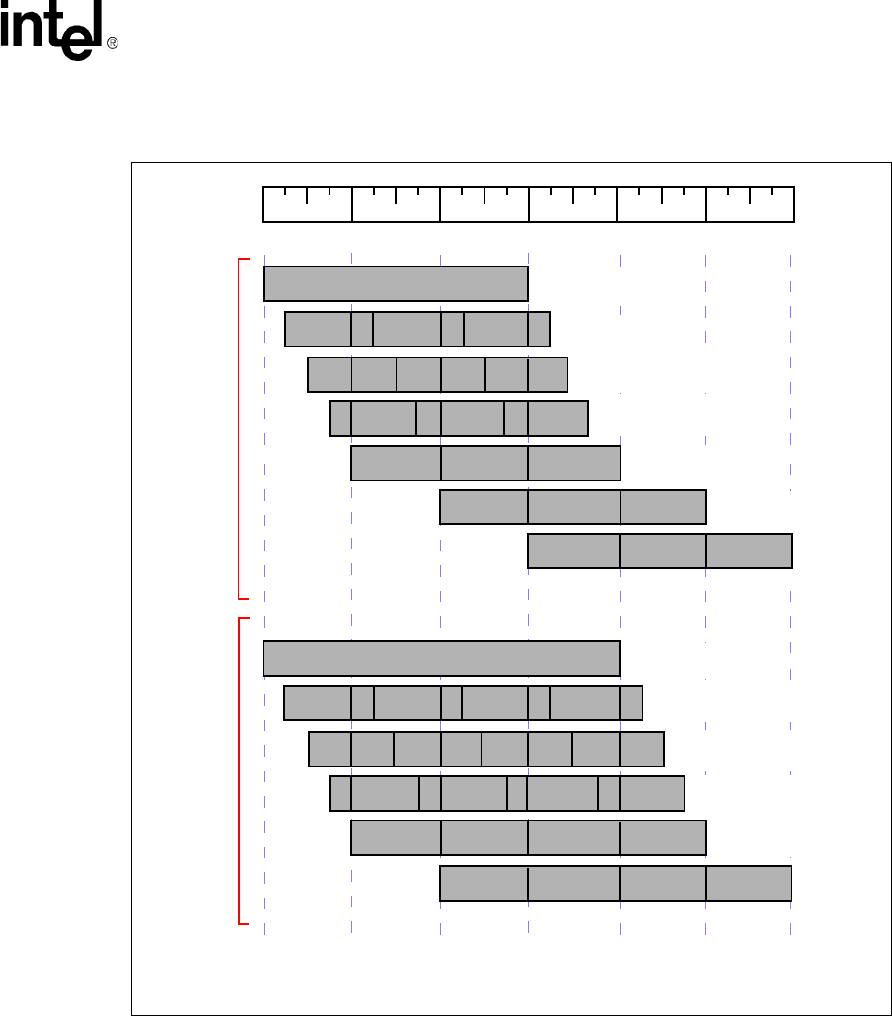
80960HA/HD/HT
Datasheet79
Figure 55. A Summary of Aligned and Unaligned Transfers for 32-Bit Regions (Continued)
04 812162024
0123456
Triple-Word
Load/Store
Quad-Word
Load/Store
Word, Word,
Word Requests
Requests
4 Word
Requests
Byte Offset
Word Offset
One Three-Word
Request (Aligned)
Trey, Byte, Trey, Byte,
Trey, Byte Requests
Short, Short, Short Requests
Short, Short, Short, Short
Byte, Trey, Byte, Trey, Byte, Trey Requests
Word, Word,
Word Requests
One Four-Word
Request (Aligned)
Trey, Byte, Trey, Byte, Trey, Byte
Trey, Byte Requests
8 Short Requests
Byte, Trey, Byte, Trey,
Byte, Trey, Byte, Trey, Requests
Requests
Word,
Word
Word,
4 Word
NOTES:
1.All requests that are less than a word in size and are cacheable will be promoted to a word to be cached. This causes
adjacent requests to occur for full words to the same address.
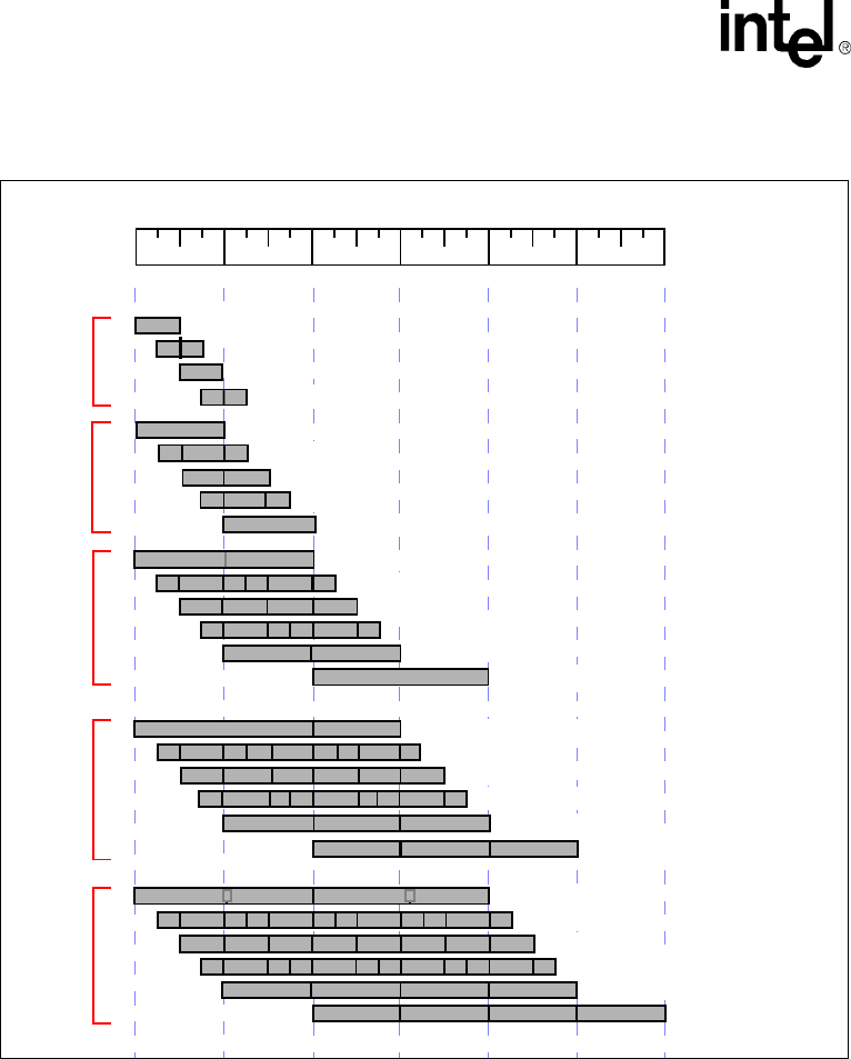
80960HA/HD/HT
80 Datasheet
Figure 56. A Summary of Aligned and Unaligned Transfers for 16-Bit Bus
04 812162024
01234 56
Byte Offset
Word Offset
Double Word
16-Bit Bus
Triple Word
16-Bit Bus
Quad Word
16-Bit Bus
Short
16-Bit Bus
Word
16-Bit Bus
Short
Four Short Burst
(Byte, Short, Byte) *2
(Short) *4
(Byte, Short, Byte)*2
Four Short Burst, Two Short Burst
(Byte, Short, Byte) *3
(Short) *6
(Byte, Short, Byte) *3
(Two Short Burst) *3
(Two Short Burst) *3
(Four Short Burst)*2
(Byte, Short, Byte) *4
(Short) *8
(Two Short Burst)*4
(Two Short Burst) *4
Short
Byte, Byte
(Byte, Short, Byte) *4
Four Short Burst
Two Short Burst
Byte, Short, Byte
(Short)*2
Two Short Burst
Byte, Short, Byte
Byte, Byte
(Two Short Burst)*2
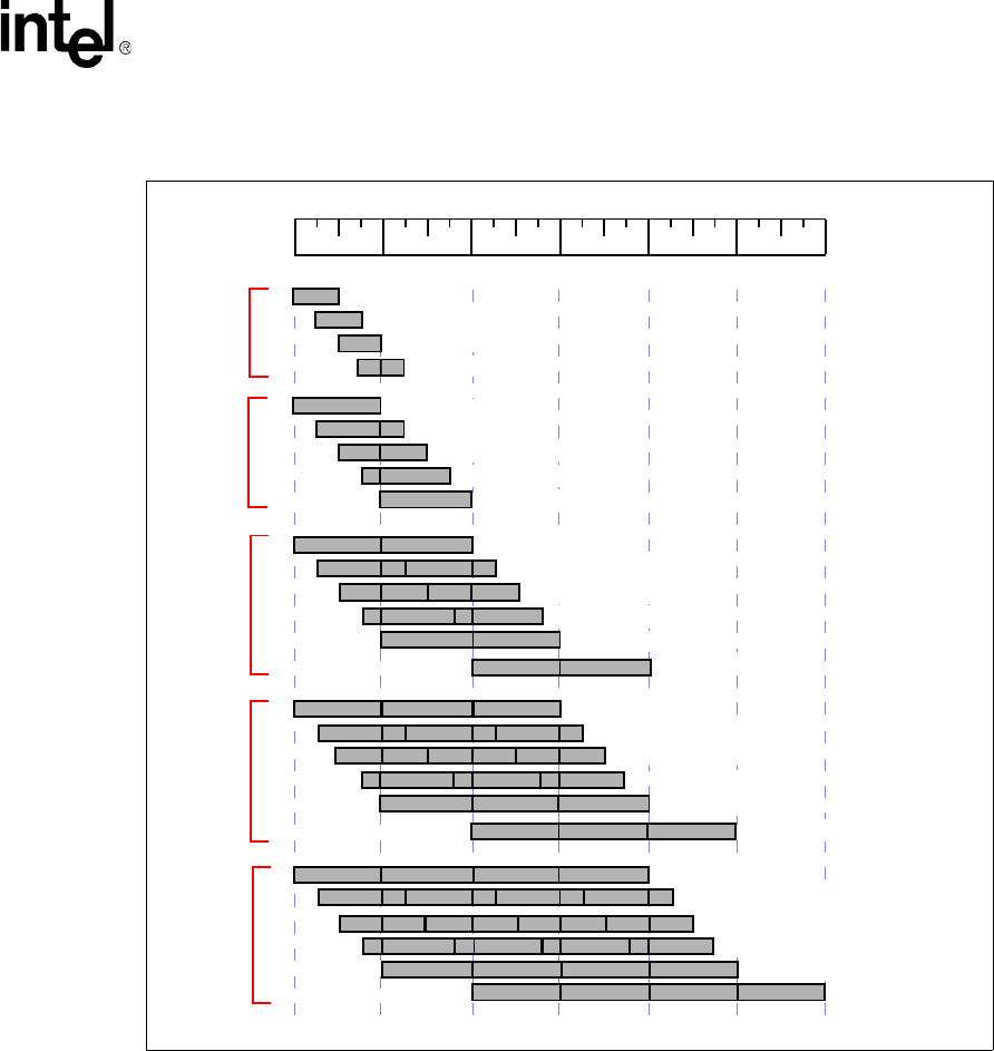
80960HA/HD/HT
Datasheet81
Figure 57. A Summary of Aligned and Unaligned Transfers for 8-Bit Bus
04 812162024
01234 56
Byte Offset
Word Offset
Short
8-Bit Bus
Word
8-Bit Bus
Triple Word
8-Bit Bus
Double Word
8-Bit Bus
Quad Word
16-Bit Bus
Two Byte Burst
Two Byte Burst
Two Byte Burst
Byte, Byte
Four Byte Burst
Three Byte Burst, Byte
(Two Byte Burst)*2
(Four Byte Burst)*3
(Two Byte Burst) *6
(Four Byte Burst)*3
Four Byte Burst
(Four Byte Burst) *2
(Three Byte Burst, Byte)*2
(Four Byte Burst) *2
(Two Byte Burst) *4
(Four Byte Burst) *2
(Three Byte Burst, Byte)*3
(Byte, Three Byte Burst) *3
(Four Byte Burst)*3
(Four Byte Burst)*4
(Two Byte Burst) *8
(Four Byte Burst)*4
(Four Byte Burst) *4
(Three Byte Burst, Byte)*4
(Byte, Three Byte Burst) *4
Byte, Three Byte Burst
(Byte, Three Byte Burst) *2
80960HA/HD/HT
82 Datasheet
Figure 58. Idle Bus Operation
CLKIN
ADS
A31:4, SUP, D/C,
LOCK
W/R
BLAST
DT/R
DEN
A3:2
WAIT
D31:0
READY,
BTERM
Write Request
NWAD=2, NXDA = 0
Ready Disabled
Idle Bus
(not in Hold Acknowledge state)
Read Request
NRAD=2, NXDA = 0
Ready Disabled
In
Out
Valid
Valid
Valid Valid
Valid Valid
PCHK
Valid Valid
BE3:0, CT3:0
80960HA/HD/HT
Datasheet83
Figure 59. Bus States
Ti = IDLE
Th = HOLD
Ta = ADDRESS
Td = DATA
Tb = BOFF’ed
Taw= address to data wait
To = ONCE
Ta
Tb
Td1
Taw2
Trw4
Tdw3
Th
Ti
To
Tdw= data to data wait
Tdw= data to address wait
!BOFF and READ and Nrdd = 0
READ and Nrdd > 0 or
WRITE and Nwdd > 0
BOFF
WdCNT = 1
!BOFF and
WaCNT = 1
WxCNT=1 and
HOLD
WxCNT > 1
BOFF
!BOFF
HOLD
HOLD
!HOLD
NOTES:
1. When the PMCON for the region has External Ready Control enabled, wait states are inserted as long
as READY and BTERM are de-asserted. When Read Pipelining is enabled, the Ta state of the
subsequent read access is concurrent with the last data cycle of the access. Because External Ready
Control is disabled for Read Pipelining, the address cycle occurs during BLAST.
2. WaCNT is decremented during Taw.
3. WdCNT is decremented during Tdw.
4. WxCNT is decremented during Trw.
!HOLD and WxCNT=1
and !REQUEST
!HOLD and WxCNT=1
and REQUEST
!RESET and
!HOLD and
REQUEST
RESET and
ONCE and
RESET
WaCNT > 1
READ and Nrad > 0 or
WRITE and Nwad > 0
!BOFF and READ and Nrad = 0 or
!BOFF and WRITE and Nwad = 0
!BOFF and READY and !BLAST or
!HOLD and BLAST and REQUEST and NXDA = 0
WdCNT > 1
KEY:
!BOFF and
and Nxda= 0
HOLD and BLAST
!BOFF and !HOLD and
Nxda = 0
BLAST and
and !BLAST or !BOFF and
WRITE and Nwdd = 0 and !BLAST or
Nxda > 0
REQUEST= One or more
requests in the bus queue.
READ= The current
access is a read.
WRITE= The current
access is a write.
RESET
BLAST and
BOFF
and !REQUEST
!ONCE
READY!
!BOFF and BTERM and !BLAST or !BOFF and

80960HA/HD/HT
84 Datasheet
5.1 80960Hx Boundary Scan Chain
Table 26. 80960Hx Boundary Scan Chain (Sheet 1 of 4)
#Boundary Scan Cell Cell TypeComment
DP3Bidirectional
DP2Bidirectional
DP0Bidirectional
DP1Bidirectional
STESTInput
FAILBAROutput
Enable for FAILBAR, BSTALL and
BREQ Control
ONCEBARInput
BOFFBAR Input
D0 Bidirectional
D1 Bidirectional
D2 Bidirectional
D3 Bidirectional
D4 Bidirectional
D5 Bidirectional
D6 Bidirectional
D7 Bidirectional
Enable for DP(3:0) and D(31:0) Control
D8 Bidirectional
D9 Bidirectional
D10 Bidirectional
D11Bidirectional
D12 Bidirectional
D13 Bidirectional
D14 Bidirectional
D15 Bidirectional
D16 Bidirectional
D17 Bidirectional
D18 Bidirectional
D19 Bidirectional
D20 Bidirectional
NOTES:
1. Cell#1 connects to TDO and cell #112 connects to TDI.
2. All outputs are tri-state.
3. In output and bidirectional signals, a logical 1 on the enable signal enables the output. A logical 0
tri-states the output.

80960HA/HD/HT
Datasheet85
D21 Bidirectional
D22 Bidirectional
D23 Bidirectional
D24 Bidirectional
D25 Bidirectional
D26 Bidirectional
D27 Bidirectional
D28 Bidirectional
D29 Bidirectional
D30 Bidirectional
D31 Bidirectional
BTERMBARInput
RDYBAR Input Appears as READYBAR in BSDL
file.
HOLD Input
HOLDAOutput
Enable for HOLDA control Control
ADSBAR Output
BE3BAR Output Appears as BEBAR(3:0) in BSDL
file.
BE2BAR Output
BE1BAR Output
BE0BAR Output
BLASTBAR Output
DENBAROutput
WRRDBAROutput Appears as WRBAR in BSDL file.
DTRBAROutput
Enable for DTRBARControl
WAITBAROutput
BSTALL Output
DATACODBAR Output Appears as DCBAR in BSDL file.
USERSUPBAR Output Appears as SUPBAR in BSDL file.
Enable for ADSBAR, BEBAR,
BLASTBAR, DENBAR, WRRDBAR,
WAITBAR, DCBAR, SUPBAR and
LOCKBAR,
Control
Table 26. 80960Hx Boundary Scan Chain (Sheet 2 of 4)
#Boundary Scan Cell Cell Type Comment
NOTES:
1. Cell#1 connects to TDO and cell #112 connects to TDI.
2. All outputs are tri-state.
3. In output and bidirectional signals, a logical 1 on the enable signal enables the output. A logical 0
tri-states the output.

80960HA/HD/HT
86 Datasheet
LOCKBAROutput
BREQ Output
A31 Output
A30 Output
A29 Output
A28 Output
A27 Output
A26 Output
A25 Output
A24 Output
A23 Output
A22 Output
A21 Output
A20 Output
A19 Output
A18 Output
A17 Output
A16 Output
Enable for A(31:0) and CT(3:0) Control
A15 Output
A14 Output
A13 Output
A12 Output
A11Output
A10 Output
A9 Output
A8 Output
A7 Output
A6 Output
A5 Output
A4 Output
A3 Output
A2 Output
NMIBARInput
Table 26. 80960Hx Boundary Scan Chain (Sheet 3 of 4)
#Boundary Scan Cell Cell TypeComment
NOTES:
1. Cell#1 connects to TDO and cell #112 connects to TDI.
2. All outputs are tri-state.
3. In output and bidirectional signals, a logical 1 on the enable signal enables the output. A logical 0
tri-states the output.

80960HA/HD/HT
Datasheet87
XINT7BAR Input Appears as XINTBAR(7:0) in
BSDL file.
XINT6BAR Input
XINT5BAR Input
XINT4BAR Input
XINT3BAR Input
XINT2BAR Input
XINT1BAR Input
XINT0BAR Input
RESETBARInput
CLKINInput
CT3Output Appears as CT(3:0) in BSDL file.
CT2Output
CT1Output
CT0Output
PCHK Output
Appears as PCHKBAR in BSDL
file.
PCHK enable Control
Table 26. 80960Hx Boundary Scan Chain (Sheet 4 of 4)
#Boundary Scan Cell Cell Type Comment
NOTES:
1. Cell#1 connects to TDO and cell #112 connects to TDI.
2. All outputs are tri-state.
3. In output and bidirectional signals, a logical 1 on the enable signal enables the output. A logical 0
tri-states the output.

80960HA/HD/HT
88 Datasheet
5.2 Boundary Scan Description Language Example
The Boundary-Scan Description Language (BSDL) for PGA Package Example, as shown in
Example 1, meets the de-facto standard means of describing essential features of ANSI/IEEE
1149.1-1993 compliant devices.
The Boundary-Scan Description Language (BSDL) for PQ2 Package Example is shown in
Example 2 on page 96.
Example 1. Boundary-Scan Description Language (BSDL) for PGA
Package Example (Sheet 1 of 8)
-- Copyright Intel Corp. 1995
- - ***************************************************************************
- - Intel Corporation makes no warranty for the use of its products and assumes no
responsibility for any errors which may appear in this document nor does it make
a commitment to update the information contained herein.
- - ***************************************************************************
- - Boundary-Scan Description Language (BSDL Version 0.0) is a de-facto standard
means of describing essential features of ANSI/IEEE 1149.1-1990 compliant
devices. This language is under consideration by the IEEE for formal inclusion
within a supplement to the 1149.1-1990 standard. The generation of the supplement
entails an extensive IEEE review and a formal acceptance balloting procedure
which may change the resultant form of the language. Be aware that this process
may extend well into 1993, and at this time the IEEE does not endorse or hold an
opinion on the language.
- - ***************************************************************************
--
-- i960(R) Processor BSDL Model

80960HA/HD/HT
Datasheet89
-- Project code HA
-- File **NOT** verified electrically
-- ------------------------------------------------
-- Rev 0.7 18 Dec 1995 Updated for A-1 stepping.
-- Rev 0.6 08 Dec 1994
-- Rev 0.5 21 Nov 1994
-- Rev 0.4 31 Oct 1994
-- Rev 0.3 26 July 1994
-- Rev 0.2 22 June 1994
-- Rev 0.1 16 Mar 1994
-- Rev 0.0 30 Aug 1993
entity Ha_Processor is
generic(PHYSICAL_PIN_MAP : string:= “PGA”);
port (A : out bit_vector(2 to 31);
ADSBAR : out bit;
BEBAR : out bit_vector(0 to 3);
BLASTBAR : out bit;
BOFFBAR : in bit;
BREQ : out bit;
BSTALL : out bit;
BTERMBAR : in bit;
CT : out bit_vector(0 to 3);
CLKIN : in bit;
D : inout bit_vector(0 to 31);
DENBAR : out bit;
DP : inout bit_vector(0 to 3);
DTRBAR : out bit;
DCBAR : out bit;
FAILBAR : out bit;
HOLD : in bit;
HOLDA : out bit;
LOCKBAR : out bit;
NMIBAR : in bit;
ONCEBAR : in bit;
PCHKBAR : out bit;
READYBAR : in bit;
RESETBAR : in bit;
STEST : in bit;
Example 1. Boundary-Scan Description Language (BSDL) for PGA
Package Example (Sheet 2 of 8)

80960HA/HD/HT
90 Datasheet
SUPBAR : out bit;
TCK : in bit;
TDI : in bit;
TDO : out bit;
TMS : in bit;
TRST : in bit;
WAITBAR : out bit;
WRBAR : out bit;
XINTBAR : in bit_vector(0 to 7);
FIVEVREF : linkage bit;
VCCPLL : linkage bit;
VOLTDET : out bit;
VCC1 : linkage bit_vector(0 to 23);
VCC2 : linkage bit_vector(0 to 20);
VSS1 : linkage bit_vector(0 to 25);
VSS2 : linkage bit_vector(0 to 22);
NC : linkage bit_vector(0 to 4)
);
use STD_1149_1_1990.all;
use i960ha_a.all;
attribute PIN_MAP of Ha_Processor : entity is PHYSICAL_PIN_MAP;
constant PGA:PIN_MAP_STRING :=
“A : (D16, D17, E16, E17, F17, G16, G17, H17, J17,”&
“ K17, L17, L16, M17, N17, N16, P17, Q17, P16,”&
“ P15, Q16, R17, R16, Q15, S17, R15, S16, Q14, ”&
“ R14, Q13, S15),
“ADSBAR : R06,”&
“BEBAR : (R09, S07, S06, S05),”&
“BLASTBAR : S08,”&
“BOFFBAR : B01,”&
“BREQ : R13,”&
“BSTALL : R12,”&
“BTERMBAR : R04,”&
“CT : (A11, A12, A13, A14),”&
“CLKIN : C13,”&
Example 1. Boundary-Scan Description Language (BSDL) for PGA
Package Example (Sheet 3 of 8)

80960HA/HD/HT
Datasheet91
“D : (E03, C02, D02, C01, E02, D01, F02, E01, F01,”&
“ G01, H02, H01, J01, K01, L02, L01, M01, N01,”&
“ N02, P01, P02, Q01, P03, Q02, R01, S01, Q03,”&
“R02, Q04, S02, Q05, R03),”&
“DENBAR : S09,”&
“DP : (A03, B03, A04, B04),”&
“DTRBAR : S11,”&
“DCBAR : S13,”&
“FAILBAR : A02,”&
“HOLD : R05,”&
“HOLDA : S04,”&
“LOCKBAR : S14,”&
“NMIBAR : D15,”&
“ONCEBAR : C03,”&
“PCHKBAR : B08,”&
“READYBAR : S03,”&
“RESETBAR : A16,”&
“STEST : B02,”&
“SUPBAR : Q12,”&
“TCK : B05,”&
“TDI : A07,”&
“TDO : A08,”&
“TMS : B06,”&
“TRST : A06,”&
“WAITBAR : S12,”&
“WRBAR : S10,”&
“ XINTBAR : (B15, A15, A17, B16, C15, B17, C16, C17),”&
“FIVEVREF : C05,”&
“VOLTDET : A05,”&
“VCCPLL : B10,”&
“ VCC1 : (M02, K02, J02, G02, N03, F03, C06, B07, B09, B11,”&
“ B12, C14, E15, F16, H16, J16, K16, M16, N15, Q06,”&
“ R07, R08, R10, R11),”&
“ VSS1 : (G03, H03, J03, K03, L03, M03, C07, C08, C09, C10,”&
“ C11, C12, Q07, Q08, Q09, Q10, Q11, F15, G15, H15,”&
“ J15, K15, L15, M15, A01, C04),”&
“NC : (A09, A10, B13, B14, D03)”;
Example 1. Boundary-Scan Description Language (BSDL) for PGA
Package Example (Sheet 4 of 8)

80960HA/HD/HT
92 Datasheet
attribute Tap_Scan_In of TDI : signal is true;
attribute Tap_Scan_Mode of TMS : signal is true;
attribute Tap_Scan_Out of TDO : signal is true;
attribute Tap_Scan_Reset of TRST : signal is true;
attribute Tap_Scan_Clock of TCK : signal is (66.0e6, BOTH);
attribute Instruction_Length of Ha_Processor: entity is 4;
attribute Instruction_Opcode of Ha_Processor: entity is
“BYPASS (1111),” &
“EXTEST (0000),” &
“SAMPLE (0001),” &
“IDCODE (0010),” &
“RUBIST (0111),” &
“CLAMP (0100),” &
“HIGHZ (1000),” &
“Reserved (1011, 1100)”;
attribute Instruction_Capture of Ha_Processor: entity is “0001”;
attribute Instruction_Private of Ha_Processor: entity is “Reserved” ;
attribute Idcode_Register of Ha_Processor: entity is
“0010”& --version,
“1000100001000000”& --part number
“00000001001”& --manufacturers identity
“1”; --required by the standard
attribute Register_Access of Ha_Processor: entity is
“Runbist[32] (RUBIST),” &
“Bypass (CLAMP, HIGHZ)”;
{***************************************************************************}
{ The first cell, cell 0, is closest to TDO }
{ BC_1:Control, Output3 CBSC_1:Bidir BC_4: Input, Clock }
{***************************************************************************}
Example 1. Boundary-Scan Description Language (BSDL) for PGA
Package Example (Sheet 5 of 8)

80960HA/HD/HT
Datasheet93
attribute Boundary_Cells of Ha_Processor: entity is “BC_4, BC_1, CBSC_1”;
attribute Boundary_Length of Ha_Processor: entity is 112;
attribute Boundary_Register of Ha_Processor: entity is
“0 (CBSC_1, DP(3), bidir, X, 17, 1, Z),” &
“1 (CBSC_1, DP(2), bidir, X, 17, 1, Z),” &
“2 (CBSC_1, DP(0), bidir, X, 17, 1, Z),” &
“3 (CBSC_1, DP(1), bidir, X, 17, 1, Z),” &
“4 (BC_4, STEST, input, X),” &
“5 (BC_1, FAILBAR, output3, X, 6, 1, Z),” &
“6 (BC_1, *, control, 1),” &
“7 (BC_4, ONCEBAR, input, X),” &
“8 (BC_4, BOFFBAR, input, X),” &
“9 (CBSC_1, D(0), bidir, X, 17, 1, Z),” &
“10 (CBSC_1, D(1), bidir, X, 17, 1, Z),” &
“11 (CBSC_1, D(2), bidir, X, 17, 1, Z),” &
“12 (CBSC_1, D(3), bidir, X, 17, 1, Z),” &
“13 (CBSC_1, D(4), bidir, X, 17, 1, Z),” &
“14 (CBSC_1, D(5), bidir, X, 17, 1, Z),” &
“15 (CBSC_1, D(6), bidir, X, 17, 1, Z),” &
“16 (CBSC_1, D(7), bidir, X, 17, 1, Z),” &
“17 (BC_1, *, control, 1),” &
“18 (CBSC_1, D(8), bidir, X, 17, 1, Z),” &
“19 (CBSC_1, D(9), bidir, X, 17, 1, Z),” &
“20 (CBSC_1, D(10), bidir, X, 17, 1, Z),” &
“21 (CBSC_1, D(11), bidir, X, 17, 1, Z),” &
“22 (CBSC_1, D(12), bidir, X, 17, 1, Z),” &
“23 (CBSC_1, D(13), bidir, X, 17, 1, Z),” &
“24 (CBSC_1, D(14), bidir, X, 17, 1, Z),” &
“25 (CBSC_1, D(15), bidir, X, 17, 1, Z),” &
“26 (CBSC_1, D(16), bidir, X, 17, 1, Z),” &
“27 (CBSC_1, D(17), bidir, X, 17, 1, Z),” &
“28 (CBSC_1, D(18), bidir, X, 17, 1, Z),” &
“29 (CBSC_1, D(19), bidir, X, 17, 1, Z),” &
“30 (CBSC_1, D(20), bidir, X, 17, 1, Z),” &
“31 (CBSC_1, D(21), bidir, X, 17, 1, Z),” &
“32 (CBSC_1, D(22), bidir, X, 17, 1, Z),” &
“33 (CBSC_1, D(23), bidir, X, 17, 1, Z),” &
“34 (CBSC_1, D(24), bidir, X, 17, 1, Z),” &
Example 1. Boundary-Scan Description Language (BSDL) for PGA
Package Example (Sheet 6 of 8)

80960HA/HD/HT
94 Datasheet
“35 (CBSC_1, D(25), bidir, X, 17, 1, Z),” &
“36 (CBSC_1, D(26), bidir, X, 17, 1, Z),” &
“37 (CBSC_1, D(27), bidir, X, 17, 1, Z),” &
“38 (CBSC_1, D(28), bidir, X, 17, 1, Z),” &
“39 (CBSC_1, D(29), bidir, X, 17, 1, Z),” &
“40 (CBSC_1, D(30), bidir, X, 17, 1, Z),” &
“41 (CBSC_1, D(31), bidir, X, 17, 1, Z),” &
“42 (BC_4, BTERMBAR, input, X),” &
“43 (BC_4, READYBAR, input, X),” &
“44 (BC_4, HOLD, input, X),” &
“45 (BC_1, HOLDA, output3, X, 46, 1, Z),” &
“46 (BC_1, *, control, 1),” &
“47 (BC_1, ADSBAR, output3, X, 61, 1, Z),” &
“48 (BC_1, BEBAR(3), output3, X, 61, 1, Z),” &
“49 (BC_1, BEBAR(2), output3, X, 61, 1, Z),” &
“50 (BC_1, BEBAR(1), output3, X, 61, 1, Z),” &
“51 (BC_1, BEBAR(0), output3, X, 61, 1, Z),” &
“52 (BC_1, BLASTBAR, output3, X, 61, 1, Z),” &
“53 (BC_1, DENBAR, output3, X, 61, 1, Z),” &
“54 (BC_1, WRBAR, output3, X, 61, 1, Z),” &
“55 (BC_1, DTRBAR, output3, X, 56, 1, Z),” &
“56 (BC_1, *, control, 1),” &
“57 (BC_1, WAITBAR, output3, X, 61, 1, Z),” &
“58 (BC_1, BSTALL, output3, X, 6, 1, Z),” &
“59 (BC_1, DCBAR, output3, X, 61, 1, Z),” &
“60 (BC_1, SUPBAR, output3, X, 61, 1, Z),” &
“61 (BC_1, *, control, 1),” &
“62 (BC_1, LOCKBAR, output3, X, 61, 1, Z),” &
“63 (BC_1, BREQ, output3, X, 6, 1, Z),” &
“64 (BC_1, A(31), output3, X, 80, 1, Z),” &
“65 (BC_1, A(30), output3, X, 80, 1, Z),” &
“66 (BC_1, A(29), output3, X, 80, 1, Z),” &
“67 (BC_1, A(28), output3, X, 80, 1, Z),” &
“68 (BC_1, A(27), output3, X, 80, 1, Z),” &
“69 (BC_1, A(26), output3, X, 80, 1, Z),” &
“70 (BC_1, A(25), output3, X, 80, 1, Z),” &
“71 (BC_1, A(24), output3, X, 80, 1, Z),” &
“72 (BC_1, A(23), output3, X, 80, 1, Z),” &
“73 (BC_1, A(22), output3, X, 80, 1, Z),” &
Example 1. Boundary-Scan Description Language (BSDL) for PGA
Package Example (Sheet 7 of 8)

80960HA/HD/HT
Datasheet95
“74 (BC_1, A(21), output3, X, 80, 1, Z),” &
“75 (BC_1, A(20), output3, X, 80, 1, Z),” &
“76 (BC_1, A(19), output3, X, 80, 1, Z),” &
“77 (BC_1, A(18), output3, X, 80, 1, Z),” &
“78 (BC_1, A(17), output3, X, 80, 1, Z),” &
“79 (BC_1, A(16), output3, X, 80, 1, Z),” &
“80 (BC_1, *, control, 1),” &
“81 (BC_1, A(15), output3, X, 80, 1, Z),” &
“82 (BC_1, A(14), output3, X, 80, 1, Z),” &
“83 (BC_1, A(13), output3, X, 80, 1, Z),” &
“84 (BC_1, A(12), output3, X, 80, 1, Z),” &
“85 (BC_1, A(11), output3, X, 80, 1, Z),” &
“86 (BC_1, A(10), output3, X, 80, 1, Z),” &
“87 (BC_1, A(9), output3, X, 80, 1, Z),” &
“88 (BC_1, A(8), output3, X, 80, 1, Z),” &
“89 (BC_1, A(7), output3, X, 80, 1, Z),” &
“90 (BC_1, A(6), output3, X, 80, 1, Z),” &
“91 (BC_1, A(5), output3, X, 80, 1, Z),” &
“92 (BC_1, A(4), output3, X, 80, 1, Z),” &
“93 (BC_1, A(3), output3, X, 80, 1, Z),” &
“94 (BC_1, A(2), output3, X, 80, 1, Z),” &
“95 (BC_4, NMIBAR, input, X),” &
“96 (BC_4, XINTBAR(7), input, X),” &
“97 (BC_4, XINTBAR(6), input, X),” &
“98 (BC_4, XINTBAR(5), input, X),” &
“99 (BC_4, XINTBAR(4), input, X),” &
“100(BC_4, XINTBAR(3), input, X),” &
“101(BC_4, XINTBAR(2), input, X),” &
“102(BC_4, XINTBAR(1), input, X),” &
“103(BC_4, XINTBAR(0), input, X),” &
“104(BC_4, RESETBAR, input, X),” &
“105(BC_4, CLKIN, input, X),” &
“106(BC_1, CT(3), output3, X, 80, 1, Z),” &
“107(BC_1, CT(2), output3, X, 80, 1, Z),” &
“108(BC_1, CT(1), output3, X, 80, 1, Z),” &
“109(BC_1, CT(0), output3, X, 80, 1, Z),” &
“110(BC_1, PCHKBAR, output3, X, 111, 1, Z),” &
“111(BC_1, *, control, 1)”;
end Ha_Processor;
Example 1. Boundary-Scan Description Language (BSDL) for PGA
Package Example (Sheet 8 of 8)

80960HA/HD/HT
96 Datasheet
Example 2. Boundary-Scan Description Language (BSDL) for PQ2
Package Example (Sheet 1 of 8)
-- Copyright Intel Corporation 1995, 1996
-- *****************************************************************************
-- Intel Corporation makes no warranty for the use of its products and assumes no
responsibility for any errors which may appear in this document nor does it make
a commitment to update the information contained herein.
-- *****************************************************************************
-- Boundary-Scan Description Language (BSDL Version 0.0) is a de-facto
-- standard means of describing essential features of ANSI/IEEE 1149.1-1990
compliant devices. This language is under consideration by the IEEE for formal
inclusion within a supplement to the 1149.1-1990 standard. The generation of the
supplement entails an extensive IEEE review and a formal acceptance balloting
procedure which may change the resultant form of the language. Be aware that this
process may extend well into 1993, and at this time the IEEE does not endorse or
hold an opinion on the language.
-- i960(R) Processor BSDL Model
-- Project code HA
-- File **NOT** verified electrically
-- -----------------------------------------------
-- Rev 0.8 4 Apr 1996 Changed for PQ2 Package
-- Rev 0.7 18 Dec 1995 Updated for A-1 stepping.
-- Rev 0.6 08 Dec 1994
-- Rev 0.5 21 Nov 1994
-- Rev 0.4 31 Oct 1994
-- Rev 0.3 26 July 1994
-- Rev 0.2 22 June 1994
-- Rev 0.1 16 Mar 1994
-- Rev 0.0 30 Aug 1993

80960HA/HD/HT
Datasheet97
entity Ha_Processor is
generic(PHYSICAL_PIN_MAP : string:= “PQ2”);
port (A : out bit_vector(2 to 31);
ADSBAR : out bit;
BEBAR : out bit_vector(0 to 3);
BLASTBAR : out bit;
BOFFBAR : in bit;
BREQ : out bit;
BSTALL : out bit;
BTERMBAR : in bit;
CT : out bit_vector(0 to 3);
CLKIN : in bit;
D : inout bit_vector(0 to 31);
DENBAR : out bit;
DP : inout bit_vector(0 to 3);
DTRBAR : out bit;
DCBAR : out bit;
FAILBAR : out bit;
HOLD : in bit;
HOLDA : out bit;
LOCKBAR : out bit;
NMIBAR : in bit;
ONCEBAR : in bit;
PCHKBAR : out bit;
READYBAR : in bit;
RESETBAR : in bit;
STEST : in bit;
SUPBAR : out bit;
TCK : in bit;
TDI : in bit;
TDO : out bit;
TMS : in bit;
TRST : in bit;
WAITBAR : out bit;
WRBAR : out bit;
XINTBAR : in bit_vector(0 to 7);
FIVEVREF : linkage bit;
VCCPLL : linkage bit;
Example 2. Boundary-Scan Description Language (BSDL) for PQ2
Package Example (Sheet 2 of 8)

80960HA/HD/HT
98 Datasheet
VCC1 : linkage bit_vector(0 to 23);
VCC2 : linkage bit_vector(0 to 23);
VSS1 : linkage bit_vector(0 to 23);
VSS2 : linkage bit_vector(0 to 23)
);
use STD_1149_1_1990.all;
use i960ha_a.all;
attribute PIN_MAP of Ha_Processor : entity is PHYSICAL_PIN_MAP;
constant PQ2:PIN_MAP_STRING :=
“A : (151, 150, 147, 146, 145, 144, 141, 140, 139, 138,”&
“ 135, 134, 133, 132, 127, 126, 125, 124, 121, 120,”&
“ 119, 118, 113, 112, 111, 110, 107, 106, 105, 104),”&
“ADSBAR : 77,”&
“BEBAR : (83, 82, 79, 78),”&
“BLASTBAR : 84,”&
“BOFFBAR : 10,”&
“BREQ : 100,”&
“BSTALL : 91,”&
“BTERMBAR : 67,”&
“CT : (183, 182, 181, 180),”&
“CLKIN : 175,”&
“D : (12, 13, 14, 15, 20, 21, 22, 23, 26, 27, 28, 29,”&
“ 34, 35, 36, 37, 39, 40, 41, 42, 45, 50, 51, 52,”&
“ 54, 55, 56, 57, 61, 62, 63, 64),”&
“DENBAR : 85,”&
“DP : (206, 207, 203, 202),”&
“DTRBAR : 89,”&
“DCBAR : 96,”&
“FAILBAR : 5,”&
“HOLD : 69,”&
“HOLDA : 72,”&
“LOCKBAR : 99,”&
“NMIBAR : 159,”&
Example 2. Boundary-Scan Description Language (BSDL) for PQ2
Package Example (Sheet 3 of 8)

80960HA/HD/HT
Datasheet99
“ONCEBAR : 6,”&
“PCHKBAR : 189,”&
“READYBAR : 68,”&
“RESETBAR : 174,”&
“STEST : 208,”&
“SUPBAR : 97,”&
“TCK : 194,”&
“TDI : 191,”&
“TDO : 188,”&
“TMS : 192,”&
“TRST : 193,”&
“WAITBAR : 90,”&
“WRBAR : 88,”&
“XINTBAR : (169, 168, 167, 166, 163, 162, 161, 160),”&
“FIVEVREF : 197,”&
“VCCPLL : 177,”&
“VCC1 : (1, 4, 9, 11, 17, 19, 25, 31, 33, 38, 44, 46,”&
“ 49, 59, 60, 66, 71, 74, 76, 81, 87, 92, 95, 101),”&
“VCC2 : (102, 109, 115, 117, 123, 128, 131, 137, 143, 149,”&
“ 153, 154, 158, 165, 171, 173, 176, 179, 185, 187,”&
“ 196, 199, 201, 204),”&
“VSS1 : (2, 3, 7, 8, 16, 18, 24, 30, 32, 43, 47, 48,”&
“ 53, 58, 65, 70, 73, 75, 80, 86, 93, 94, 98, 103),”&
“VSS2 : (108, 114, 116, 122, 129, 130, 136, 142, 148, 152,”&
“ 155, 156, 157, 164, 170, 172, 178, 184, 186, 190,”&
“ 195, 198, 200, 205)”;
attribute Tap_Scan_In of TDI : signal is true;
attribute Tap_Scan_Mode of TMS : signal is true;
attribute Tap_Scan_Out of TDO : signal is true;
attribute Tap_Scan_Reset of TRST : signal is true;
attribute Tap_Scan_Clock of TCK : signal is (66.0e6, BOTH);
attribute Instruction_Length of Ha_Processor: entity is 4;
attribute Instruction_Opcode of Ha_Processor: entity is
Example 2. Boundary-Scan Description Language (BSDL) for PQ2
Package Example (Sheet 4 of 8)

80960HA/HD/HT
100 Datasheet
“BYPASS (1111),” &
“EXTEST (0000),” &
“SAMPLE (0001),” &
“IDCODE (0010),” &
“RUBIST (0111),” &
“CLAMP (0100),” &
“HIGHZ (1000),” &
“Reserved (1011, 1100)”;
attribute Instruction_Capture of Ha_Processor: entity is “0001”;
attribute Instruction_Private of Ha_Processor: entity is “Reserved” ;
attribute Idcode_Register of Ha_Processor: entity is
“0001”& version,
“1000100001000000”& part number
“00000001001”& manufacturers identity
“1”; required by the standard
attribute Register_Access of Ha_Processor: entity is
“Runbist[32] (RUBIST),” &
“Bypass (CLAMP, HIGHZ)”;
*******************************************************************************
{ The first cell, cell 0, is closest to TDO }
{ BC_1:Control, Output3 CBSC_1:Bidir BC_4: Input, Clock }
*******************************************************************************
attribute Boundary_Cells of Ha_Processor: entity is “BC_4, BC_1, CBSC_1”;
attribute Boundary_Length of Ha_Processor: entity is 112;
attribute Boundary_Register of Ha_Processor: entity is
“0 (CBSC_1, DP(3), bidir, X, 17, 1, Z),” &
“1 (CBSC_1, DP(2), bidir, X, 17, 1, Z),” &
“2 (CBSC_1, DP(0), bidir, X, 17, 1, Z),” &
“3 (CBSC_1, DP(1), bidir, X, 17, 1, Z),” &
“4 (BC_4, STEST, input, X),” &
“5 (BC_1, FAILBAR, output3, X, 6, 1, Z),” &
Example 2. Boundary-Scan Description Language (BSDL) for PQ2
Package Example (Sheet 5 of 8)

80960HA/HD/HT
Datasheet101
“6 (BC_1, *, control, 1),” &
“7 (BC_4, ONCEBAR, input, X),” &
“8 (BC_4, BOFFBAR, input, X),” &
“9 (CBSC_1, D(0), bidir, X, 17, 1, Z),” &
“10 (CBSC_1, D(1), bidir, X, 17, 1, Z),” &
“11 (CBSC_1, D(2), bidir, X, 17, 1, Z),” &
“12 (CBSC_1, D(3), bidir, X, 17, 1, Z),” &
“13 (CBSC_1, D(4), bidir, X, 17, 1, Z),” &
“14 (CBSC_1, D(5), bidir, X, 17, 1, Z),” &
“15 (CBSC_1, D(6), bidir, X, 17, 1, Z),” &
“16 (CBSC_1, D(7), bidir, X, 17, 1, Z),” &
“17 (BC_1, *, control, 1),” &
“18 (CBSC_1, D(8), bidir, X, 17, 1, Z),” &
“19 (CBSC_1, D(9), bidir, X, 17, 1, Z),” &
“20 (CBSC_1, D(10), bidir, X, 17, 1, Z),” &
“21 (CBSC_1, D(11), bidir, X, 17, 1, Z),” &
“22 (CBSC_1, D(12), bidir, X, 17, 1, Z),” &
“23 (CBSC_1, D(13), bidir, X, 17, 1, Z),” &
“24 (CBSC_1, D(14), bidir, X, 17, 1, Z),” &
“25 (CBSC_1, D(15), bidir, X, 17, 1, Z),” &
“26 (CBSC_1, D(16), bidir, X, 17, 1, Z),” &
“27 (CBSC_1, D(17), bidir, X, 17, 1, Z),” &
“28 (CBSC_1, D(18), bidir, X, 17, 1, Z),” &
“29 (CBSC_1, D(19), bidir, X, 17, 1, Z),” &
“30 (CBSC_1, D(20), bidir, X, 17, 1, Z),” &
“31 (CBSC_1, D(21), bidir, X, 17, 1, Z),” &
“32 (CBSC_1, D(22), bidir, X, 17, 1, Z),” &
“33 (CBSC_1, D(23), bidir, X, 17, 1, Z),” &
“34 (CBSC_1, D(24), bidir, X, 17, 1, Z),” &
“35 (CBSC_1, D(25), bidir, X, 17, 1, Z),” &
“36 (CBSC_1, D(26), bidir, X, 17, 1, Z),” &
“37 (CBSC_1, D(27), bidir, X, 17, 1, Z),” &
“38 (CBSC_1, D(28), bidir, X, 17, 1, Z),” &
“39 (CBSC_1, D(29), bidir, X, 17, 1, Z),” &
“40 (CBSC_1, D(30), bidir, X, 17, 1, Z),” &
Example 2. Boundary-Scan Description Language (BSDL) for PQ2
Package Example (Sheet 6 of 8)

80960HA/HD/HT
102 Datasheet
“41 (CBSC_1, D(31), bidir, X, 17, 1, Z),” &
“42 (BC_4, BTERMBAR, input, X),” &
“43 (BC_4, READYBAR, input, X),” &
“44 (BC_4, HOLD, input, X),” &
“45 (BC_1, HOLDA, output3, X, 46, 1, Z),” &
“46 (BC_1, *, control, 1),” &
“47 (BC_1, ADSBAR, output3, X, 61, 1, Z),” &
“48 (BC_1, BEBAR(3), output3, X, 61, 1, Z),” &
“49 (BC_1, BEBAR(2), output3, X, 61, 1, Z),” &
“50 (BC_1, BEBAR(1), output3, X, 61, 1, Z),” &
“51 (BC_1, BEBAR(0), output3, X, 61, 1, Z),” &
“52 (BC_1, BLASTBAR, output3, X, 61, 1, Z),” &
“53 (BC_1, DENBAR, output3, X, 61, 1, Z),” &
“54 (BC_1, WRBAR, output3, X, 61, 1, Z),” &
“55 (BC_1, DTRBAR, output3, X, 56, 1, Z),” &
“56 (BC_1, *, control, 1),” &
“57 (BC_1, WAITBAR, output3, X, 61, 1, Z),” &
“58 (BC_1, BSTALL, output3, X, 6, 1, Z),” &
“59 (BC_1, DCBAR, output3, X, 61, 1, Z),” &
“60 (BC_1, SUPBAR, output3, X, 61, 1, Z),” &
“61 (BC_1, *, control, 1),” &
“62 (BC_1, LOCKBAR, output3, X, 61, 1, Z),” &
“63 (BC_1, BREQ, output3, X, 6, 1, Z),” &
“64 (BC_1, A(31), output3, X, 80, 1, Z),” &
“65 (BC_1, A(30), output3, X, 80, 1, Z),” &
“66 (BC_1, A(29), output3, X, 80, 1, Z),” &
“67 (BC_1, A(28), output3, X, 80, 1, Z),” &
“68 (BC_1, A(27), output3, X, 80, 1, Z),” &
“69 (BC_1, A(26), output3, X, 80, 1, Z),” &
“70 (BC_1, A(25), output3, X, 80, 1, Z),” &
“71 (BC_1, A(24), output3, X, 80, 1, Z),” &
“72 (BC_1, A(23), output3, X, 80, 1, Z),” &
“73 (BC_1, A(22), output3, X, 80, 1, Z),” &
“74 (BC_1, A(21), output3, X, 80, 1, Z),” &
“75 (BC_1, A(20), output3, X, 80, 1, Z),” &
Example 2. Boundary-Scan Description Language (BSDL) for PQ2
Package Example (Sheet 7 of 8)

80960HA/HD/HT
Datasheet103
“76 (BC_1, A(19), output3, X, 80, 1, Z),” &
“77 (BC_1, A(18), output3, X, 80, 1, Z),” &
“78 (BC_1, A(17), output3, X, 80, 1, Z),” &
“79 (BC_1, A(16), output3, X, 80, 1, Z),” &
“80 (BC_1, *, control, 1),” &
“81 (BC_1, A(15), output3, X, 80, 1, Z),” &
“82 (BC_1, A(14), output3, X, 80, 1, Z),” &
“83 (BC_1, A(13), output3, X, 80, 1, Z),” &
“84 (BC_1, A(12), output3, X, 80, 1, Z),” &
“85 (BC_1, A(11), output3, X, 80, 1, Z),” &
“86 (BC_1, A(10), output3, X, 80, 1, Z),” &
“87 (BC_1, A(9), output3, X, 80, 1, Z),” &
“88 (BC_1, A(8), output3, X, 80, 1, Z),” &
“89 (BC_1, A(7), output3, X, 80, 1, Z),” &
“90 (BC_1, A(6), output3, X, 80, 1, Z),” &
“91 (BC_1, A(5), output3, X, 80, 1, Z),” &
“92 (BC_1, A(4), output3, X, 80, 1, Z),” &
“93 (BC_1, A(3), output3, X, 80, 1, Z),” &
“94 (BC_1, A(2), output3, X, 80, 1, Z),” &
“95 (BC_4, NMIBAR, input, X),” &
“96 (BC_4, XINTBAR(7), input, X),” &
“97 (BC_4, XINTBAR(6), input, X),” &
“98 (BC_4, XINTBAR(5), input, X),” &
“99 (BC_4, XINTBAR(4), input, X),” &
“100(BC_4, XINTBAR(3), input, X),” &
“101(BC_4, XINTBAR(2), input, X),” &
“102(BC_4, XINTBAR(1), input, X),” &
“103(BC_4, XINTBAR(0), input, X),” &
“104(BC_4, RESETBAR, input, X),” &
“105(BC_4, CLKIN, input, X),” &
“106(BC_1, CT(3), output3, X, 80, 1, Z),” &
“107(BC_1, CT(2), output3, X, 80, 1, Z),” &
“108(BC_1, CT(1), output3, X, 80, 1, Z),” &
“109(BC_1, CT(0), output3, X, 80, 1, Z),” &
“110(BC_1, PCHKBAR, output3, X, 111,1, Z),” &
“111(BC_1, *, control, 1)”;
end Ha_Processor;
Example 2. Boundary-Scan Description Language (BSDL) for PQ2
Package Example (Sheet 8 of 8)

80960HA/HD/HT
104 Datasheet
This page intentionally left blank.
