Intel IXF1104 IXF1104_CSpec_Datasheet_Book User Manual To The 205ea831 77a6 4d70 Bf39 Cb66a5381fb4
User Manual: Intel IXF1104 to the manual
Open the PDF directly: View PDF ![]() .
.
Page Count: 227 [warning: Documents this large are best viewed by clicking the View PDF Link!]
- 1.0 Introduction
- 2.0 General Description
- 3.0 Ball Assignments and Ball List Tables
- 4.0 Ball Assignments and Signal Descriptions
- 4.1 Naming Conventions
- 4.2 Interface Signal Groups
- 4.3 Signal Description Tables
- Table 3. SPI3 Interface Signal Descriptions (Sheet 1 of 8)
- Table 4. SerDes Interface Signal Descriptions
- Table 5. GMII Interface Signal Descriptions (Sheet 1 of 2)
- Table 6. RGMII Interface Signal Descriptions (Sheet 1 of 2)
- Table 7. CPU Interface Signal Descriptions (Sheet 1 of 2)
- Table 8. Transmit Pause Control Interface Signal Descriptions
- Table 9. Optical Module Interface Signal Descriptions (Sheet 1 of 2)
- Table 10. MDIO Interface Signal Descriptions
- Table 11. LED Interface Signal Descriptions
- Table 12. JTAG Interface Signal Descriptions
- Table 13. System Interface Signal Descriptions
- Table 14. Power Supply Signal Descriptions
- 4.4 Ball Usage Summary
- 4.5 Multiplexed Ball Connections
- 4.6 Ball State During Reset
- 4.7 Power Supply Sequencing
- 4.8 Pull-Up/Pull-Down Ball Guidelines
- 4.9 Analog Power Filtering
- 5.0 Functional Descriptions
- 5.1 Media Access Controller (MAC)
- 5.2 SPI3 Interface
- 5.3 Gigabit Media Independent Interface (GMII)
- 5.4 Reduced Gigabit Media Independent Interface (RGMII)
- 5.5 MDIO Control and Interface
- 5.6 SerDes Interface
- 5.7 Optical Module Interface
- 5.7.1 IXF1104-Supported Optical Module Interface Signals
- 5.7.2 Functional Descriptions
- 5.7.3 I·C Module Configuration Interface
- 5.8 LED Interface
- 5.9 CPU Interface
- 5.10 TAP Interface (JTAG)
- 5.11 Loopback Modes
- 5.12 Clocks
- 6.0 Applications
- 7.0 Electrical Specifications
- Table 39. Absolute Maximum Ratings
- Table 40. Recommended Operating Conditions
- 7.1 DC Specifications
- 7.2 SPI3 AC Timing Specifications
- 7.3 RGMII AC Timing Specification
- 7.4 GMII AC Timing Specification
- 7.5 SerDes AC Timing Specification
- 7.6 MDIO AC Timing Specification
- 7.7 Optical Module and I2C AC Timing Specification
- 7.8 CPU AC Timing Specification
- 7.9 Transmit Pause Control AC Timing Specification
- 7.10 JTAG AC Timing Specification
- 7.11 System AC Timing Specification
- 7.12 LED AC Timing Specification
- 8.0 Register Set
- 8.1 Document Structure
- 8.2 Graphical Representation
- 8.3 Per Port Registers
- 8.4 Register Map
- Table 59. MAC Control Registers ($ Port Index + Offset) (Sheet 1 of 2)
- Table 60. MAC RX Statistics Registers ($ Port Index + Offset) (Sheet 1 of 2)
- Table 61. MAC TX Statistics Registers ($ Port Index + Offset)
- Table 62. PHY Autoscan Registers ($ Port Index + Offset)
- Table 63. Global Status and Configuration Registers ($ 0x500 - 0X50C)
- Table 64. RX FIFO Registers ($ 0x580 - 0x5BF) (Sheet 1 of 2)
- Table 65. TX FIFO Registers ($ 0x600 - 0x63E) (Sheet 1 of 2)
- Table 66. MDIO Registers ($ 0x680 - 0x683)
- Table 67. SPI3 Registers ($ 0x700 - 0x716) (Sheet 1 of 2)
- Table 68. SerDes Registers ($ 0x780 - 0x798)
- Table 69. Optical Module Registers ($ 0x799 - 0x79F)
- 8.4.1 MAC Control Registers
- Table 70. Station Address ($ Port_Index +0x00 - +0x01)
- Table 71. Desired Duplex ($ Port_Index + 0x02)
- Table 72. FD FC Type ($ Port_Index + 0x03)
- Table 73. Collision Distance ($ Port_Index + 0x05)
- Table 74. Collision Threshold ($ Port_Index + 0x06)
- Table 75. FC TX Timer Value ($ Port_Index + 0x07)
- Table 76. FD FC Address ($ Port_Index + 0x08 - + 0x09)
- Table 77. IPG Receive Time 1 ($ Port_Index + 0x0A)
- Table 78. IPG Receive Time 2 ($ Port_Index + 0x0B)
- Table 79. IPG Transmit Time ($ Port_Index + 0x0C)
- Table 80. Pause Threshold ($ Port_Index + 0x0E)
- Table 81. Max Frame Size (Addr: Port_Index + 0x0F)
- Table 82. MAC IF Mode and RGMII Speed ($ Port_Index + 0x10)
- Table 83. Flush TX ($ Port_Index + 0x11)
- Table 84. FC Enable ($ Port_Index + 0x12)
- Table 85. FC Back Pressure Length ($ Port_Index + 0x13)
- Table 86. Short Runts Threshold ($ Port_Index + 0x14)
- Table 87. Discard Unknown Control Frame ($ Port_Index + 0x15)
- Table 88. RX Config Word ($ Port_Index + 0x16) (Sheet 1 of 2)
- Table 89. TX Config Word ($ Port_Index + 0x17) (Sheet 1 of 2)
- Table 90. Diverse Config Write ($ Port_Index + 0x18) (Sheet 1 of 2)
- Table 91. RX Packet Filter Control ($ Port_Index + 0x19) (Sheet 1 of 2)
- Table 92. Port Multicast Address ($ Port_Index +0x1A - +0x1B)
- 8.4.2 MAC RX Statistics Register Overview
- 8.4.3 MAC TX Statistics Register Overview
- 8.4.4 PHY Autoscan Registers
- Table 95. PHY Control ($ Port Index + 0x60) (Sheet 1 of 2)
- Table 96. PHY Status ($ Port Index + 0x61) (Sheet 1 of 2)
- Table 97. PHY Identification 1 ($ Port Index + 0x62)
- Table 98. PHY Identification 2 ($ Port Index + 0x63) (Sheet 1 of 2)
- Table 99. Auto-Negotiation Advertisement ($ Port Index + 0x64) (Sheet 1 of 2)
- Table 100. Auto-Negotiation Link Partner Base Page Ability ($ Port Index + 0x65) (Sheet 1 of 2)
- Table 101. Auto-Negotiation Expansion ($ Port Index + 0x66)
- Table 102. Auto-Negotiation Next Page Transmit ($ Port Index + 0x67)
- 8.4.5 Global Status and Configuration Register Overview
- Table 103. Port Enable ($0x500)
- Table 104. Interface Mode ($0x501)
- Table 105. Link LED Enable ($0x502)
- Table 106. MAC Soft Reset ($0x505)
- Table 107. MDIO Soft Reset ($0x506)
- Table 108. CPU Interface ($0x508)
- Table 109. LED Control ($0x509)
- Table 110. LED Flash Rate ($0x50A)
- Table 111. LED Fault Disable ($0x50B)
- Table 112. JTAG ID ($0x50C)
- 8.4.6 RX FIFO Register Overview
- Table 113. RX FIFO High Watermark Port 0 ($0x580)
- Table 114. RX FIFO High Watermark Port 1 ($0x581)
- Table 115. RX FIFO High Watermark Port 2 ($0x582)
- Table 116. RX FIFO High Watermark Port 3 ($0x583)
- Table 117. RX FIFO Low Watermark Port 0 ($0x58A)
- Table 118. RX FIFO Low Watermark Port 1 ($0x58B)
- Table 119. RX FIFO Low Watermark Port 2 ($0x58C)
- Table 120. RX FIFO Low Watermark Port 3 ($0x58D)
- Table 121. RX FIFO Overflow Frame Drop Counter Ports 0 - 3 ($0x594 - 0x597)
- Table 122. RX FIFO Port Reset ($0x59E)
- Table 123. RX FIFO Errored Frame Drop Enable ($0x59F)
- Table 124. RX FIFO Overflow Event ($0x5A0)
- Table 125. RX FIFO Errored Frame Drop Counter Ports 0 - 3 ($0x5A2 - 0x5A5) (Sheet 1 of 2)
- Table 126. RX FIFO SPI3 Loopback Enable for Ports 0 - 3 ($0x5B2)
- Table 127. RX FIFO Padding and CRC Strip Enable ($0x5B3)
- Table 128. RX FIFO Transfer Threshold Port 0 ($0x5B8)
- Table 129. RX FIFO Transfer Threshold Port 1 ($0x5B9)
- Table 130. RX FIFO Transfer Threshold Port 2 ($0x5BA)
- Table 131. RX FIFO Transfer Threshold Port 3 ($0x5BB)
- 8.4.7 TX FIFO Register Overview
- Table 132. TX FIFO High Watermark Ports 0 - 3 ($0x600 - 0x603)
- Table 133. TX FIFO Low Watermark Register Ports 0 - 3 ($0x60A - 0x60D)
- Table 134. TX FIFO MAC Threshold Register Ports 0 - 3 ($0x614 - 0x617)
- Table 135. TX FIFO Overflow/Underflow/Out of Sequence Event ($0x61E) (Sheet 1 of 2)
- Table 136. Loop RX Data to TX FIFO (Line-Side Loopback) Ports 0 - 3 ($0x61F)
- Table 137. TX FIFO Port Reset ($0x620) (Sheet 1 of 2)
- Table 138. TX FIFO Overflow Frame Drop Counter Ports 0 - 3 ($0x621 - 0x624)
- Table 139. TX FIFO Errored Frame Drop Counter Ports 0 - 3 ($0x625 - 0x629)
- Table 140. TX FIFO Occupancy Counter for Ports 0 - 3 ($0x62D - 0x630)
- Table 141. TX FIFO Port Drop Enable ($0x63D)
- 8.4.8 MDIO Register Overview
- 8.4.9 SPI3 Register Overview
- 8.4.10 SerDes Register Overview
- 8.4.11 Optical Module Register Overview
- 9.0 Mechanical Specifications
- 10.0 Product Ordering Information

Intel® IXF1104 4-Port Gigabit Ethernet
Media Access Controller
Datasheet
The Intel® IXF1104 is a four-port Gigabit MAC that supports IEEE 802.3 10/100/1000 Mbps
applications. The IXF1104 supports a System Packet Interface Phase 3 (SPI3) system interface
to a network processor or ASIC, and concurrently supports copper and fiber physical layer
devices (PHYs).
The copper PHY interface implements the Gigabit Media Independent Interface (GMII) and the
Reduced Gigabit Media Independent Interface (RGMII) as defined in Version 1.2a of the
Hewlett-Packard* specification. RGMII has the benefit of reducing the PHY interface pin count
for high-port-count applications.
The fiber PHY interface implements an internal Serializer/Deserializer (SerDes) on each port to
allow direct connection to optical modules. The integration of the SerDes functionality reduces
PCB area requirements and system cost.
Product Features
4 Independent Ethernet MAC Ports which
support 3 interfaces for Copper or Fiber
Physical layer connectivity.
—IEEE 802.3 compliant
—RMON Statistics
—Independent Enable/Disable of any port
Copper Mode:
—RGMII for 10/100/1000 Mbps
connections
—GMII for 1000 Mbps full-duplex
connectivity
—IEEE 802.3 MDIO interface
Fiber Mode:
—Integrated SerDes interface for direct
connection to optical modules for
1000BASE-X connectivity
—Supports IEEE 802.3 fiber auto-
negotiation including forced mode
—Small Form Factor Pluggable (SFP)
Transceiver MSA compatible
System Packet Interface Level 3 (SPI3)
—Capable of data transfers at 4 Gbps in
both SPI3 modes:
32-bit Multi-PHY mode (133 Mhz)
4 x 8bit Single-PHY mode (125 Mhz)
Operating Temperature Ranges:
MIN MAX
Copper Mode: -40°C +85°C
Fiber Mode: 0°C +70°C
Flexible 32/16/8-bit CPU interface
Programmable Packet handling
—Filter packets with errors
—Filter broadcast, multicast, unicast and
VLAN packets
—Automatically pad transmitted packets
less than the minimum frame size
—Remove CRC from packets received
Performance Monitoring and Diagnostics
—CRC calculation and error detection
—Detection of length error, runt or overly
large packets
—Counters for dropped and errored
packets
—Loopback modes
—JTAG- and boundary-scan-capable
IEEE 802.3 Complaint Flow Control
—Loss-less flow control for up to 9.6 KB
packets and 5 km of fiber
—Jumbo frame support for 9.6 KB packets
Internal 32 KB receive FIFO and 10 KB
transmit FIFOs per channel
552-ball Ceramic Ball Grid Array (CBGA)
—1.8 V core, 2.5 V RGMII, GMII, OMI,
and 3.3 V SPI3 and CPU
—.18 µ CMOS process technology
Product Ordering Number:
HFIXF1104CE.B0 853714
Document Number: 278757
Revision Number: 007
Revision Date:
March 25, 2004

2Datasheet
Document Number: 278757
Revision Number: 007
Revision Date: March 25, 2004
Applications
Load Balancing Systems
MultiService Switch
Web Caching Appliances
Intelligent Backplane Interfaces
Edge Router
Base Station Controller
Redundant Line Cards
Base Transceiver Station
Serving GRPS Support Node (SGSN)
General Packet Radio Services (GGSN)
Packet Data Serving Note (PDSN)
Digital Subscriber Line Access Multiplexer
(DSLAM)
Cable Modem Termination System
(CMTS)
INFORMATION IN THIS DOCUMENT IS PROVIDED IN CONNECTION WITH INTEL® PRODUCTS. NO LICENSE, EXPRESS OR IMPLIED, BY
ESTOPPEL OR OTHERWISE, TO ANY INTELLECTUAL PROPERTY RIGHTS IS GRANTED BY THIS DOCUMENT. EXCEPT AS PROVIDED IN
INTEL'S TERMS AND CONDITIONS OF SALE FOR SUCH PRODUCTS, INTEL ASSUMES NO LIABILITY WHATSOEVER, AND INTEL DISCLAIMS
ANY EXPRESS OR IMPLIED WARRANTY, RELATING TO SALE AND/OR USE OF INTEL PRODUCTS INCLUDING LIABILITY OR WARRANTIES
RELATING TO FITNESS FOR A PARTICULAR PURPOSE, MERCHANTABILITY, OR INFRINGEMENT OF ANY PATENT, COPYRIGHT OR OTHER
INTELLECTUAL PROPERTY RIGHT. Intel products are not intended for use in medical, life saving, life sustaining, critical control or safety systems, or
in nuclear facility applications.
Intel may make changes to specifications and product descriptions at any time, without notice.
Designers must not rely on the absence or characteristics of any features or instructions marked “reserved” or “undefined.” Intel reserves these for
future definition and shall have no responsibility whatsoever for conflicts or incompatibilities arising from future changes to them.
The Intel® IXF1104 Media Access Controller may contain design defects or errors known as errata which may cause the product to deviate from
published specifications. Current characterized errata are available on request.
Contact your local Intel sales office or your distributor to obtain the latest specifications and before placing your product order.
Copies of documents which have an ordering number and are referenced in this document, or other Intel literature may be obtained by calling
1-800-548-4725 or by visiting Intel's website at http://www.intel.com.
AnyPoint, AppChoice, BoardWatch, BunnyPeople, CablePort, Celeron, Chips, CT Media, Dialogic, DM3, EtherExpress, ETOX, FlashFile, i386, i486,
i960, iCOMP, InstantIP, Intel, Intel Centrino, Intel logo, Intel386, Intel486, Intel740, IntelDX2, IntelDX4, IntelSX2, Intel Create & Share, Intel GigaBlade,
Intel InBusiness, Intel Inside, Intel Inside logo, Intel NetBurst, Intel NetMerge, Intel NetStructure, Intel Play, Intel Play logo, Intel SingleDriver, Intel
SpeedStep, Intel StrataFlash, Intel TeamStation, Intel Xeon, Intel XScale, IPLink, Itanium, MCS, MMX, MMX logo, Optimizer logo, OverDrive,
Paragon, PC Dads, PC Parents, PDCharm, Pentium, Pentium II Xeon, Pentium III Xeon, Performance at Your Command, RemoteExpress, SmartDie,
Solutions960, Sound Mark, StorageExpress, The Computer Inside., The Journey Inside, TokenExpress, VoiceBrick, VTune, and Xircom are
trademarks or registered trademarks of Intel Corporation or its subsidiaries in the United States and other countries.
*Other names and brands may be claimed as the property of others.
Copyright © 2004, Intel Corporation

Contents
Datasheet 3
Document Number: 278757
Revision Number: 007
Revision Date: March 25, 2004
Contents
1.0 Introduction..................................................................................................................................19
1.1 What You Will Find in This Document ................................................................................19
1.2 Related Documents ............................................................................................................19
2.0 General Description ....................................................................................................................20
3.0 Ball Assignments and Ball List Tables......................................................................................22
3.1 Ball Assignments ................................................................................................................22
3.2 Ball List Tables ...................................................................................................................23
3.2.1 Balls Listed in Alphabetic Order by Signal Name ..................................................23
3.2.2 Balls Listed in Alphabetic Order by Ball Location ..................................................29
4.0 Ball Assignments and Signal Descriptions ..............................................................................36
4.1 Naming Conventions ..........................................................................................................36
4.1.1 Signal Name Conventions .....................................................................................36
4.1.2 Register Address Conventions ..............................................................................36
4.2 Interface Signal Groups ......................................................................................................37
4.3 Signal Description Tables ...................................................................................................38
4.4 Ball Usage Summary ..........................................................................................................56
4.5 Multiplexed Ball Connections..............................................................................................57
4.5.1 GMII/RGMII/SerDes/OMI Multiplexed Ball Connections........................................57
4.5.2 SPI3 MPHY/SPHY Ball Connections.....................................................................58
4.6 Ball State During Reset ......................................................................................................60
4.7 Power Supply Sequencing..................................................................................................62
4.7.1 Power-Up Sequence..............................................................................................62
4.7.2 Power-Down Sequence .........................................................................................62
4.8 Pull-Up/Pull-Down Ball Guidelines......................................................................................63
4.9 Analog Power Filtering........................................................................................................63
5.0 Functional Descriptions..............................................................................................................65
5.1 Media Access Controller (MAC) .........................................................................................65
5.1.1 Features for Fiber and Copper Mode ....................................................................66
5.1.1.1 Padding of Undersized Frames on Transmit .........................................66
5.1.1.2 Automatic CRC Generation ...................................................................66
5.1.1.3 Filtering of Receive Packets ..................................................................66
5.1.1.4 CRC Error Detection ..............................................................................68
5.1.2 Flow Control...........................................................................................................68
5.1.2.1 802.3x Flow Control (Full-Duplex Operation).........................................69
5.1.3 Mixed-Mode Operation ..........................................................................................74
5.1.3.1 Configuration of the IXF1104 .................................................................74
5.1.3.2 Key Configuration Registers ..................................................................74
5.1.4 Fiber Mode.............................................................................................................75
5.1.4.1 Fiber Auto-Negotiation...........................................................................76
5.1.4.2 Determining If Link Is Established in Auto-Negotiation Mode ................76
5.1.4.3 Fiber Forced Mode.................................................................................76
5.1.4.4 Determination of Link Establishment in Forced Mode ...........................76
5.1.5 Copper Mode .........................................................................................................76

Contents
4Datasheet
Document Number: 278757
Revision Number: 007
Revision Date: March 25, 2004
5.1.5.1 Speed.....................................................................................................77
5.1.5.2 Duplex....................................................................................................77
5.1.5.3 Copper Auto-Negotiation .......................................................................77
5.1.6 Jumbo Packet Support ..........................................................................................77
5.1.6.1 Rx Statistics ...........................................................................................78
5.1.6.2 TX Statistics...........................................................................................78
5.1.6.3 Loss-less Flow Control...........................................................................78
5.1.7 Packet Buffer Dimensions .....................................................................................79
5.1.7.1 TX and RX FIFO Operation ...................................................................79
5.1.8 RMON Statistics Support.......................................................................................79
5.1.8.1 Conventions...........................................................................................81
5.1.8.2 IXF1104 Advantages .............................................................................82
5.2 SPI3 Interface.....................................................................................................................82
5.2.1 MPHY Operation....................................................................................................83
5.2.1.1 SPI3 RX Round Robin Data Transmission ............................................83
5.2.2 MPHY Logical Timing ............................................................................................83
5.2.2.1 Transmit Timing .....................................................................................84
5.2.2.2 Receive Timing ......................................................................................84
5.2.2.3 Clock Rates............................................................................................86
5.2.2.4 Parity......................................................................................................86
5.2.2.5 SPHY Mode ...........................................................................................86
5.2.2.6 SPHY Logical Timing.............................................................................87
5.2.2.7 Transmit Timing (SPHY)........................................................................87
5.2.2.8 Receive Timing (SPHY).........................................................................87
5.2.2.9 SPI3 Flow Control..................................................................................90
5.2.3 Pre-Pending Function............................................................................................92
5.3 Gigabit Media Independent Interface (GMII) ......................................................................92
5.3.1 GMII Signal Multiplexing........................................................................................93
5.3.2 GMII Interface Signal Definition.............................................................................93
5.4 Reduced Gigabit Media Independent Interface (RGMII) ....................................................95
5.4.1 Multiplexing of Data and Control............................................................................95
5.4.2 Timing Specifics.....................................................................................................96
5.4.3 TX_ER and RX_ER Coding...................................................................................96
5.4.3.1 In-Band Status .......................................................................................98
5.4.4 10/100 Mbps Functionality.....................................................................................98
5.5 MDIO Control and Interface................................................................................................98
5.5.1 MDIO Address.......................................................................................................99
5.5.2 MDIO Register Descriptions ..................................................................................99
5.5.3 Clear When Done..................................................................................................99
5.5.4 MDC Generation....................................................................................................99
5.5.4.1 MDC High-Frequency Operation ...........................................................99
5.5.4.2 MDC Low-Frequency Operation ............................................................99
5.5.5 Management Frames...........................................................................................100
5.5.6 Single MDI Command Operation.........................................................................100
5.5.7 MDI State Machine ..............................................................................................100
5.5.8 Autoscan Operation.............................................................................................102
5.6 SerDes Interface...............................................................................................................102
5.6.1 Features...............................................................................................................102
5.6.2 Functional Description.........................................................................................102
5.6.2.1 Transmitter Operational Overview .......................................................103
5.6.2.2 Transmitter Programmable Driver-Power Levels.................................103

Contents
Datasheet 5
Document Number: 278757
Revision Number: 007
Revision Date: March 25, 2004
5.6.2.3 Receiver Operational Overview ...........................................................104
5.6.2.4 Selective Power-Down.........................................................................104
5.6.2.5 Receiver Jitter Tolerance.....................................................................104
5.6.2.6 Transmit Jitter ......................................................................................105
5.6.2.7 Receive Jitter .......................................................................................105
5.7 Optical Module Interface...................................................................................................106
5.7.1 IXF1104-Supported Optical Module Interface Signals.........................................106
5.7.2 Functional Descriptions .......................................................................................107
5.7.2.1 High-Speed Serial Interface.................................................................107
5.7.2.2 Low-Speed Status Signaling Interface.................................................107
5.7.3 I²C Module Configuration Interface......................................................................109
5.7.3.1 I2C Control and Data Registers............................................................109
5.7.3.2 I2C Read Operation..............................................................................109
5.7.3.3 I2C Write Operation..............................................................................110
5.7.3.4 I²C Protocol Specifics...........................................................................111
5.7.3.5 Port Protocol Operation .......................................................................111
5.7.3.6 Clock and Data Transitions..................................................................111
5.8 LED Interface....................................................................................................................114
5.8.1 Modes of Operation .............................................................................................114
5.8.2 LED Interface Signal Description.........................................................................114
5.8.3 Mode 0: Detailed Operation.................................................................................115
5.8.4 Mode 1: Detailed Operation.................................................................................116
5.8.5 Power-On, Reset, Initialization ............................................................................117
5.8.6 LED DATA Decodes............................................................................................117
5.8.6.1 LED Signaling Behavior .......................................................................118
5.9 CPU Interface ...................................................................................................................119
5.9.1 Functional Description .........................................................................................120
5.9.1.1 Read Access........................................................................................120
5.9.1.2 Write Access ........................................................................................120
5.9.1.3 CPU Timing Parameters......................................................................121
5.9.2 Endian..................................................................................................................121
5.10 TAP Interface (JTAG) .......................................................................................................122
5.10.1 TAP State Machine..............................................................................................122
5.10.2 Instruction Register and Supported Instructions..................................................123
5.10.3 ID Register...........................................................................................................124
5.10.4 Boundary Scan Register......................................................................................124
5.10.5 Bypass Register...................................................................................................124
5.11 Loopback Modes ..............................................................................................................124
5.11.1 SPI3 Interface Loopback .....................................................................................124
5.11.2 Line Side Interface Loopback ..............................................................................125
5.12 Clocks...............................................................................................................................126
5.12.1 System Interface Reference Clocks.....................................................................126
5.12.1.1 CLK125 ................................................................................................127
5.12.2 SPI3 Receive and Transmit Clocks .....................................................................127
5.12.3 RGMII Clocks.......................................................................................................127
5.12.4 MDC Clock...........................................................................................................127
5.12.5 JTAG Clock..........................................................................................................128
5.12.6 I2C Clock..............................................................................................................128
5.12.7 LED Clock............................................................................................................128

Contents
6Datasheet
Document Number: 278757
Revision Number: 007
Revision Date: March 25, 2004
6.0 Applications...............................................................................................................................129
6.1 Change Port Mode Initialization Sequence.......................................................................129
7.0 Electrical Specifications ...........................................................................................................131
7.1 DC Specifications .............................................................................................................132
7.1.1 Undershoot / Overshoot Specifications ...............................................................134
7.1.2 RGMII Electrical Characteristics..........................................................................134
7.2 SPI3 AC Timing Specifications.........................................................................................136
7.2.1 Receive Interface Timing.....................................................................................136
7.2.2 Transmit Interface Timing....................................................................................138
7.3 RGMII AC Timing Specification ........................................................................................140
7.4 GMII AC Timing Specification...........................................................................................141
7.4.1 1000 Base-T Operation .......................................................................................141
7.4.1.1 1000 BASE-T Transmit Interface.........................................................141
7.4.1.2 1000BASE-T Receive Interface...........................................................142
7.5 SerDes AC Timing Specification.......................................................................................143
7.6 MDIO AC Timing Specification.........................................................................................144
7.6.1 MDC High-Speed Operation Timing....................................................................144
7.6.2 MDC Low-Speed Operation Timing.....................................................................144
7.6.3 MDIO AC Timing..................................................................................................145
7.7 Optical Module and I2C AC Timing Specification .............................................................146
7.7.1 I2C Interface Timing.............................................................................................146
7.8 CPU AC Timing Specification...........................................................................................148
7.8.1 CPU Interface Read Cycle AC Timing.................................................................148
7.8.2 CPU Interface Write Cycle AC Timing.................................................................148
7.9 Transmit Pause Control AC Timing Specification.............................................................150
7.10 JTAG AC Timing Specification .........................................................................................151
7.11 System AC Timing Specification.......................................................................................152
7.12 LED AC Timing Specification............................................................................................153
8.0 Register Set................................................................................................................................154
8.1 Document Structure..........................................................................................................154
8.2 Graphical Representation.................................................................................................154
8.3 Per Port Registers ............................................................................................................155
8.4 Register Map ....................................................................................................................155
8.4.1 MAC Control Registers........................................................................................162
8.4.2 MAC RX Statistics Register Overview.................................................................173
8.4.3 MAC TX Statistics Register Overview .................................................................177
8.4.4 PHY Autoscan Registers.....................................................................................180
8.4.5 Global Status and Configuration Register Overview ...........................................187
8.4.6 RX FIFO Register Overview ................................................................................192
8.4.7 TX FIFO Register Overview.................................................................................202
8.4.8 MDIO Register Overview.....................................................................................210
8.4.9 SPI3 Register Overview.......................................................................................212
8.4.10 SerDes Register Overview ..................................................................................219
8.4.11 Optical Module Register Overview ......................................................................221
9.0 Mechanical Specifications........................................................................................................223
9.1 Overview........................................................................................................................... 223
9.1.1 Features...............................................................................................................223

Contents
Datasheet 7
Document Number: 278757
Revision Number: 007
Revision Date: March 25, 2004
9.2 Package Specifics for the IXF1104...................................................................................223
9.3 Package Information.........................................................................................................224
9.3.1 Example Package Marking ..................................................................................226
10.0 Product Ordering Information ..................................................................................................227
Figures
1 Block Diagram ............................................................................................................................20
2 Internal Architecture....................................................................................................................21
3Intel
® IXF1104 552-Ball CBGA Assignments (Top View)...........................................................22
4 Interface Signals ........................................................................................................................37
5 Power Supply Sequencing..........................................................................................................62
6 Analog Power Supply Filter Network ..........................................................................................64
7 Packet Buffering FIFO ................................................................................................................70
8 Ethernet Frame Format ..............................................................................................................70
9 PAUSE Frame Format................................................................................................................71
10 Transmit Pause Control Interface...............................................................................................73
11 MPHY Transmit Logical Timing ..................................................................................................84
12 MPHY Receive Logical Timing ...................................................................................................85
13 MPHY 32-Bit Interface................................................................................................................85
14 SPHY Transmit Logical Timing...................................................................................................87
15 SPHY Receive Logical Timing....................................................................................................88
16 SPHY Connection for Two IXF1104 Ports (8-Bit Interface)........................................................89
17 MAC GMII Interconnect ..............................................................................................................93
18 RGMII Interface ..........................................................................................................................95
19 TX_CTL Behavior .......................................................................................................................97
20 RX_CTL Behavior.......................................................................................................................97
21 Management Frame Structure (Single-Frame Format) ............................................................100
22 MDI State..................................................................................................................................101
23 SerDes Receiver Jitter Tolerance.............................................................................................105
24 I2C Random Read Transaction.................................................................................................110
25 Data Validity Timing..................................................................................................................112
26 Start and Stop Definition Timing...............................................................................................112
27 Acknowledge Timing.................................................................................................................113
28 Random Read...........................................................................................................................114
29 Mode 0 Timing..........................................................................................................................115
30 Mode 1 Timing..........................................................................................................................117
31 Read Timing Diagram - Asynchronous Interface......................................................................120
32 Write Timing Diagram - Asynchronous Interface......................................................................121
33 SPI3 Interface Loopback Path..................................................................................................125
34 Line Side Interface Loopback Path...........................................................................................126
35 SPI3 Receive Interface Timing .................................................................................................136
36 SPI3 Transmit Interface Timing ................................................................................................138
37 RGMII Interface Timing.............................................................................................................140
38 1000BASE-T Transmit Interface Timing...................................................................................141
39 1000BASE-T Receive Interface Timing....................................................................................142
40 SerDes Timing Diagram ...........................................................................................................143
41 MDC High-Speed Operation Timing .........................................................................................144
42 MDC Low-Speed Operation Timing..........................................................................................144

Contents
8Datasheet
Document Number: 278757
Revision Number: 007
Revision Date: March 25, 2004
43 MDIO Write Timing Diagram ....................................................................................................145
44 MDIO Read Timing Diagram ....................................................................................................145
45 Bus Timing Diagram .................................................................................................................146
46 Write Cycle Diagram.................................................................................................................146
47 CPU Interface Read Cycle AC Timing......................................................................................148
48 CPU Interface Write Cycle AC Timing......................................................................................148
49 Pause Control Interface Timing................................................................................................150
50 JTAG AC Timing.......................................................................................................................151
51 System Reset AC Timing .........................................................................................................152
52 LED AC Interface Timing..........................................................................................................153
53 Memory Overview Diagram ......................................................................................................154
54 Register Overview Diagram......................................................................................................155
55 CBGA Package Diagram..........................................................................................................224
56 CBGA Package Side View Diagram.........................................................................................225
57 Intel® IXF1104 Example Package Marking ..............................................................................226
58 Ordering Information – Sample ................................................................................................227
Tables
1 Ball List in Alphanumeric Order by Signal Name........................................................................23
2 Ball List in Alphanumeric Order by Ball Location........................................................................29
3 SPI3 Interface Signal Descriptions.............................................................................................38
4 SerDes Interface Signal Descriptions.........................................................................................46
5 GMII Interface Signal Descriptions.............................................................................................47
6 RGMII Interface Signal Descriptions ..........................................................................................49
7 CPU Interface Signal Descriptions .............................................................................................50
9 Optical Module Interface Signal Descriptions.............................................................................52
8 Transmit Pause Control Interface Signal Descriptions...............................................................52
10 MDIO Interface Signal Descriptions ...........................................................................................53
11 LED Interface Signal Descriptions..............................................................................................54
12 JTAG Interface Signal Descriptions............................................................................................54
13 System Interface Signal Descriptions.........................................................................................54
14 Power Supply Signal Descriptions..............................................................................................55
15 Ball Usage Summary.................................................................................................................. 56
16 Line Side Interface Multiplexed Balls..........................................................................................57
17 SPI3 MPHY/SPHY Interface....................................................................................................... 58
18 Definition of Output and Bi-directional Balls During Hardware Reset.........................................60
19 Power Supply Sequencing .........................................................................................................63
20 Pull-Up/Pull-Down and Unused Ball Guidelines .........................................................................63
21 Analog Power Balls .................................................................................................................... 64
22 CRC Errored Packets Drop Enable Behavior.............................................................................68
23 Valid Decodes for TXPAUSEADD[2:0].......................................................................................73
24 Operational Mode Configuration Registers ................................................................................75
25 RMON Additional Statistics ........................................................................................................80
26 GMII Interface Signal Definitions................................................................................................94
27 RGMII Signal Definitions ............................................................................................................96
28 TX_ER and RX_ER Coding Description.....................................................................................96
29 SerDes Driver TX Power Levels...............................................................................................103
30 IXF1104-to-SFP Optical Module Interface Connections...........................................................106
31 LED Interface Signal Descriptions............................................................................................115
32 Mode 0 Clock Cycle to Data Bit Relationship...........................................................................116

Contents
Datasheet 9
Document Number: 278757
Revision Number: 007
Revision Date: March 25, 2004
33 Mode 1 Clock Cycle to Data Bit Relationship ...........................................................................117
34 LED_DATA# Decodes..............................................................................................................118
35 LED Behavior (Fiber Mode)......................................................................................................118
36 LED Behavior (Copper Mode) ..................................................................................................119
37 Byte Swapper Behavior ............................................................................................................122
38 Instruction Register Description................................................................................................123
39 Absolute Maximum Ratings......................................................................................................131
40 Recommended Operating Conditions.......................................................................................132
41 Intel® IXF1104 MAC DC Specifications ...................................................................................133
42 SerDes Transmit Characteristics..............................................................................................133
43 Intel® IXF1104 MAC SerDes Receive Characteristics.............................................................134
44 Undershoot / Overshoot Limits .................................................................................................134
45 RGMII Power ............................................................................................................................135
46 SPI3 Receive Interface Signal Parameters ..............................................................................137
47 SPI3 Transmit Interface Signal Parameters .............................................................................139
48 RGMII Interface Timing Parameters.........................................................................................140
49 GMII 1000BASE-T Transmit Signal Parameters ......................................................................141
50 GMII 1000BASE-T Receive Signal Parameters .......................................................................142
51 SerDes Timing Parameters ......................................................................................................143
52 MDIO Timing Parameters.........................................................................................................145
53 I2C AC Timing Characteristics..................................................................................................146
54 CPU Interface Write Cycle AC Signal Parameters ...................................................................149
55 Transmit Pause Control Interface Timing Parameters..............................................................150
56 JTAG AC Timing Parameters ...................................................................................................151
57 System Reset AC Timing Parameters......................................................................................152
58 LED Interface AC Timing Parameters ......................................................................................153
59 MAC Control Registers ($ Port Index + Offset) ........................................................................155
60 MAC RX Statistics Registers ($ Port Index + Offset)................................................................156
61 MAC TX Statistics Registers ($ Port Index + Offset) ................................................................157
62 PHY Autoscan Registers ($ Port Index + Offset)......................................................................158
63 Global Status and Configuration Registers ($ 0x500 - 0X50C) ................................................158
64 RX FIFO Registers ($ 0x580 - 0x5BF)......................................................................................158
65 TX FIFO Registers ($ 0x600 - 0x63E) ......................................................................................159
66 MDIO Registers ($ 0x680 - 0x683)...........................................................................................160
67 SPI3 Registers ($ 0x700 - 0x716).............................................................................................160
68 SerDes Registers ($ 0x780 - 0x798) ........................................................................................161
69 Optical Module Registers ($ 0x799 - 0x79F) ............................................................................161
70 Station Address ($ Port_Index +0x00 – +0x01)........................................................................162
71 Desired Duplex ($ Port_Index + 0x02) .....................................................................................162
72 FD FC Type ($ Port_Index + 0x03) ..........................................................................................162
73 Collision Distance ($ Port_Index + 0x05) .................................................................................163
74 Collision Threshold ($ Port_Index + 0x06) ...............................................................................163
75 FC TX Timer Value ($ Port_Index + 0x07) ...............................................................................163
76 FD FC Address ($ Port_Index + 0x08 – + 0x09) ......................................................................163
77 IPG Receive Time 1 ($ Port_Index + 0x0A) .............................................................................164
78 IPG Receive Time 2 ($ Port_Index + 0x0B) .............................................................................164
79 IPG Transmit Time ($ Port_Index + 0x0C) ...............................................................................164
80 Pause Threshold ($ Port_Index + 0x0E) ..................................................................................165
81 Max Frame Size (Addr: Port_Index + 0x0F) .............................................................................165
82 MAC IF Mode and RGMII Speed ($ Port_Index + 0x10) ..........................................................166

Contents
10 Datasheet
Document Number: 278757
Revision Number: 007
Revision Date: March 25, 2004
83 Flush TX ($ Port_Index + 0x11)................................................................................................166
84 FC Enable ($ Port_Index + 0x12).............................................................................................167
85 FC Back Pressure Length ($ Port_Index + 0x13).....................................................................167
86 Short Runts Threshold ($ Port_Index + 0x14)..........................................................................168
87 Discard Unknown Control Frame ($ Port_Index + 0x15)..........................................................168
88 RX Config Word ($ Port_Index + 0x16)....................................................................................168
89 TX Config Word ($ Port_Index + 0x17) ....................................................................................169
90 Diverse Config Write ($ Port_Index + 0x18).............................................................................170
91 RX Packet Filter Control ($ Port_Index + 0x19) .......................................................................171
92 Port Multicast Address ($ Port_Index +0x1A – +0x1B) ............................................................172
93 MAC RX Statistics ($ Port_Index + 0x20 – + 0x39)..................................................................173
94 MAC TX Statistics ($ Port_Index +0x40 – +0x58) ....................................................................177
95 PHY Control ($ Port Index + 0x60)...........................................................................................180
96 PHY Status ($ Port Index + 0x61) ............................................................................................181
97 PHY Identification 1 ($ Port Index + 0x62) ...............................................................................182
98 PHY Identification 2 ($ Port Index + 0x63) ...............................................................................182
99 Auto-Negotiation Advertisement ($ Port Index + 0x64) ............................................................183
100 Auto-Negotiation Link Partner Base Page Ability ($ Port Index + 0x65)...................................184
101 Auto-Negotiation Expansion ($ Port Index + 0x66) ..................................................................185
102 Auto-Negotiation Next Page Transmit ($ Port Index + 0x67) ...................................................186
103 Port Enable ($0x500)................................................................................................................187
104 Interface Mode ($0x501) ..........................................................................................................187
105 Link LED Enable ($0x502)........................................................................................................188
106 MAC Soft Reset ($0x505).........................................................................................................188
107 MDIO Soft Reset ($0x506) .......................................................................................................189
108 CPU Interface ($0x508)............................................................................................................189
109 LED Control ($0x509)...............................................................................................................189
110 LED Flash Rate ($0x50A).........................................................................................................190
111 LED Fault Disable ($0x50B).....................................................................................................190
112 JTAG ID ($0x50C)....................................................................................................................191
113 RX FIFO High Watermark Port 0 ($0x580)...............................................................................192
114 RX FIFO High Watermark Port 1 ($0x581)...............................................................................192
115 RX FIFO High Watermark Port 2 ($0x582)...............................................................................192
116 RX FIFO High Watermark Port 3 ($0x583)...............................................................................193
117 RX FIFO Low Watermark Port 0 ($0x58A)...............................................................................193
118 RX FIFO Low Watermark Port 1 ($0x58B)...............................................................................193
119 RX FIFO Low Watermark Port 2 ($0x58C)...............................................................................194
120 RX FIFO Low Watermark Port 3 ($0x58D)...............................................................................194
121 RX FIFO Overflow Frame Drop Counter Ports 0 - 3 ($0x594 – 0x597)....................................194
122 RX FIFO Port Reset ($0x59E)..................................................................................................195
123 RX FIFO Errored Frame Drop Enable ($0x59F).......................................................................195
124 RX FIFO Overflow Event ($0x5A0) ..........................................................................................196
125 RX FIFO Errored Frame Drop Counter Ports 0 - 3 ($0x5A2 - 0x5A5)......................................197
126 RX FIFO SPI3 Loopback Enable for Ports 0 - 3 ($0x5B2) .......................................................198
127 RX FIFO Padding and CRC Strip Enable ($0x5B3) .................................................................199
128 RX FIFO Transfer Threshold Port 0 ($0x5B8)..........................................................................200
129 RX FIFO Transfer Threshold Port 1 ($0x5B9)..........................................................................200
130 RX FIFO Transfer Threshold Port 2 ($0x5BA) .........................................................................201
131 RX FIFO Transfer Threshold Port 3 ($0x5BB) .........................................................................201
132 TX FIFO High Watermark Ports 0 - 3 ($0x600 – 0x603) ..........................................................202

Contents
Datasheet 11
Document Number: 278757
Revision Number: 007
Revision Date: March 25, 2004
133 TX FIFO Low Watermark Register Ports 0 - 3 ($0x60A – 0x60D)............................................203
134 TX FIFO MAC Threshold Register Ports 0 - 3 ($0x614 – 0x617).............................................204
135 TX FIFO Overflow/Underflow/Out of Sequence Event ($0x61E)..............................................205
136 Loop RX Data to TX FIFO (Line-Side Loopback) Ports 0 - 3 ($0x61F) ...................................206
137 TX FIFO Port Reset ($0x620)...................................................................................................206
138 TX FIFO Overflow Frame Drop Counter Ports 0 - 3 ($0x621 – 0x624) ....................................207
139 TX FIFO Errored Frame Drop Counter Ports 0 - 3 ($0x625 – 0x629) ......................................208
140 TX FIFO Occupancy Counter for Ports 0 - 3 ($0x62D – 0x630)...............................................209
141 TX FIFO Port Drop Enable ($0x63D)........................................................................................209
142 MDIO Single Command ($0x680).............................................................................................210
143 MDIO Single Read and Write Data ($0x681)............................................................................210
144 Autoscan PHY Address Enable ($0x682).................................................................................211
145 MDIO Control ($0x683).............................................................................................................211
146 SPI3 Transmit and Global Configuration ($0x700) ...................................................................212
147 SPI3 Receive Configuration ($0x701) ......................................................................................214
148 Address Parity Error Packet Drop Counter ($0x70A) ...............................................................218
149 TX Driver Power Level Ports 0 - 3 ($0x784).............................................................................219
150 TX and RX Power-Down ($0x787) ...........................................................................................219
151 RX Signal Detect Level Ports 0 - 3 ($0x793) ............................................................................219
152 Clock and Interface Mode Change Enable Ports 0 - 3 ($0x794) ..............................................220
153 Optical Module Status Ports 0-3 ($0x799)................................................................................221
154 Optical Module Control Ports 0 - 3 ($0x79A) ............................................................................221
155 I2C Control Ports 0 - 3 ($0x79B)...............................................................................................222
156 I2C Data Ports 0 - 3 ($0x79F)...................................................................................................222
157 Product Information ..................................................................................................................227

Contents
12 Datasheet
Document Number: 278757
Revision Number: 007
Revision Date: March 25, 2004
Revision History
Revision Number: 007
Revision Date: March 25, 2004
(Sheet 1 of 5)
Page # Description
All Globally replaced GBIC with Optical Module Interface.
All Globally edited signal names.
All
Globally changed SerDes and PLL analog power ball names as follows:
TXAVTT and RXAVTT changed to AVDD1P8_2
TXAV25 and RXAV25 changed to AVDD2P5_2
PLL1_VDDA and PLL2_VDDA changed to AVDD1P8_1
PLL3_VDDA changed to AVDD2P5_1
PLL1_GNDA, PLL2_GNDA, and PLL3_GNDA changed to GND
1Reworded and rearranged the Product Features section on page one
Changed Jumbo frame support from “10 kbytes” to “9.6 KB”.
20 Changed heading to Section 2.0, “General Description” [was Section 2.0, “Block Diagram”].
22/36 Reversed sections as follows:
Section 3.0, “Ball Assignments and Ball List Tables”
Section 4.0, “Ball Assignments and Signal Descriptions”
23
Modified Table 1 “Ball List in Alphanumeric Order by Signal Name”:
Changed A10 from VCC to VDD
Changed C12 from VCC to VDD
Changed D11 from VCC to VDD
Changed J20 from GND to VDD
Changed Ball A1 from NC to No Pad.
Changed Balls A2, A3, A22, A23, A24, B1, B2, B23, B24, C1, C24, AB1, AB24, AC1, AC2, AC23,
AC24, AD1, AD2, AD3, AD22, AD23, AD24 from NC to No Ball.
29
Modified Table 2 “Ball List in Alphanumeric Order by Ball Location”
Changed A10 from VCC to VDD
Changed C12 form VCC to VDD
Changed D11 from VCC to VDD
Changed J20 from GND to VDD
Changed Ball A1 from NC to No Pad.
Changed Balls A2, A3, A22, A23, A24, B1, B2, B23, B24, C1, C24, AB1, AB24, AC1, AC2, AC23,
AC24, AD1, AD2, AD3, AD22, AD23, AD24 from NC to No Ball.
37 Updated Figure 4 “Interface Signals” [modified SPI3 interface signals and added MPHY and SPHY
categories; modified signal names].
38 Broke old Table 1, “IXF1104 Signal Descriptions” into the following:
Table 3 “SPI3 Interface Signal Descriptions” on page 38 through Table 14 “Power Supply Signal
Descriptions” on page 55
38 Modified Table 3 “SPI3 Interface Signal Descriptions” on page 38 [edited description for DTPA;
added text to TFCLK description; added text to RFCLK description].
49 Modified Table 6 “RGMII Interface Signal Descriptions” [Added Ball Designators; added notes
under descriptions].
50 Modified Table 7 “CPU Interface Signal Descriptions” [UPX_DATA[16]: deleted J10, added M10].
52 Modified Table 9 “Optical Module Interface Signal Descriptions” [added Ball Designators].
53 Modified Table 10 “MDIO Interface Signal Descriptions” [moved note from MDC to MDIO].
55 Modified Table 14 “Power Supply Signal Descriptions” [added Ball Designators A4, A21, and AD21
to GND; added AVDD1P8_1, AVDD1P8_2, AVDD2P5_1, and AVDD2P5_2].

Contents
Datasheet 13
Document Number: 278757
Revision Number: 007
Revision Date: March 25, 2004
38 Modified Section 4.3, “Signal Description Tables” [changed heading from “Signal Naming
Conventions; added new headings Section 4.1.1, “Signal Name Conventions” and Section 4.1.2,
“Register Address Conventions”; and added/enhanced material under headings.
57 Added new Section 4.5, “Multiplexed Ball Connections” with Table 16 “Line Side Interface
Multiplexed Balls” and Table 17 “SPI3 MPHY/SPHY Interface”.
62 Modified Section 4.7, “Power Supply Sequencing” [changed language under this section and added
Section 4.7.1, “Power-Up Sequence” and Section 4.7.2, “Power-Down Sequence”].
62 Modified Table 5 “Power Supply Sequencing” [deleted 3.3 V Supplies Stable; changed Apply 1.8 V
to VDD, AVDD1P8_1, and AVDD1P8_2; changed Apply 2.5 V to AVDD2P5_1 and AVDD2P5_2].
60 Modified Table 18 “Definition of Output and Bi-directional Balls During Hardware Reset” [changed
comments for Optical Modules].
63 Modified Table 20 “Pull-Up/Pull-Down and Unused Ball Guidelines” [changed TRST_L to pull-down;
added MDIO, UPX_RDY_L, I2C_DATA_3:0, and TX_DISABLE_3:0].
63 Added new Section 4.9, “Analog Power Filtering” [including Figure 6 “Analog Power Supply Filter
Network” on page 64 and Table 21 “Analog Power Balls” on page 64].
65 Modified/edited text under Section 5.1, “Media Access Controller (MAC)” [rearranged and created
new bullets].
66 Modified first paragraph under Section 5.1.1.1, “Padding of Undersized Frames on Transmit”.
66 Modified entire Section 5.1.1.3, “Filtering of Receive Packets”.
67 Added new Section 5.1.1.3.6, “Filter CRC Error Packets”.
68 Added note under Table 22 “CRC Errored Packets Drop Enable Behavior”.
68 Added new Section 5.1.2, “Flow Control” including Figure 7 “Packet Buffering FIFO”, Figure 8
“Ethernet Frame Format”, and Figure 9 “PAUSE Frame Format”.
72 Replaced Section 5.1.2.1.5, “Transmit Pause Control Interface” [added Table 23 “Valid Decodes for
TXPAUSEADD[2:0]” and modified Table 10 “Transmit Pause Control Interface”.
73 Modified Figure 10 “Transmit Pause Control Interface”
74 Added note under Section 5.1.3.1, “Configuration of the IXF1104”.
75 Added table note to Table 24 “Operational Mode Configuration Registers”.
76 Added note under Section 5.1.4.3, “Fiber Forced Mode”.
78 Modified Section 5.1.6.2, “TX Statistics” [added text to third sentence in first paragraph].
78 Modified Section 5.1.6.3, “Loss-less Flow Control” [changed “two kilometers” to “five kilometers” in
last sentence.
79 Modified Section 5.1.7.1.2, “RX FIFO” [changed 10 KB to 9.6 KB; added text to last paragraph].
82 Rewrote/replaced Section 5.2, “SPI3 Interface”.
85 Edited signal names in Figure 13 “MPHY 32-Bit Interface”.
89 Edited signal names in Figure 16 “SPHY Connection for Two IXF1104 Ports (8-Bit Interface)”.
90 Added new Section 5.2.2.9, “SPI3 Flow Control”.
[Removed old “Packet-Level and Byte-Level Transfers” section.}
93 Modified Figure 17 “MAC GMII Interconnect” [edited signal names].
NA Removed old Section 5.3.3 Electrical Requirements and Table 27 “Electrical Requirements” –
changed Input high current Max from 40 to 15 and Input low current Min from -600 to -15.
95 Added a note under Section 5.4, “Reduced Gigabit Media Independent Interface (RGMII)”.
95 Modified Figure 18 “RGMII Interface” [edited signal names].
97 Modified Figure 19 “TX_CTL Behavior” [changed signal names].
Revision Number: 007
Revision Date: March 25, 2004
(Sheet 2 of 5)
Page # Description

Contents
14 Datasheet
Document Number: 278757
Revision Number: 007
Revision Date: March 25, 2004
97 Modified Figure 20 “RX_CTL Behavior” [changed signal names].
98 Modified Section 5.5, “MDIO Control and Interface” [changed 3.3 us to 3.3 ms in fourth paragraph,
third sentence].
102 Modified/replaced all text under Section 5.6, “SerDes Interface” on page 102 [added Table 29
“SerDes Driver TX Power Levels”].
NA Removed old Section 5.6.2.4 AC/DC Coupling.
NA Removed old Section 5.6.2.9 System Jitter.
106 Modified Table 30 “IXF1104-to-SFP Optical Module Interface Connections” [edited signal names].
106 Modified/replaced text and deleted old “Figure 19. Typical GBIC Module Functional Diagram” under
Section 5.7, “Optical Module Interface”].
107 Modified second sentence under Section 5.7.2.2.1, “MOD_DEF_0:3”.
108 Modified second sentence under Section 5.7.2.2.3, “RX_LOS_0:3”.
108 Removed third paragraph under Section 5.7.2.2.7, “RX_LOS_INT”.
109 Modified first and second paragraphs under Section 5.7.3, “I²C Module Configuration Interface”.
110 Modified Section 5.7.3.3, “I2C Write Operation” [edited portions of text].
115 Modified Table 31 “LED Interface Signal Descriptions” [changed 0.5 MHz to 720 Hz for LED_CLK
under Signal Description].
118 Modified Table 35 “LED Behavior (Fiber Mode)” [changed links under Description to “Link LED
Enable ($0x502)”].
NA Removed old Figure 30 “CPU – External and Internal Connections”.
122 Modified Table 37 “Byte Swapper Behavior” [edited/added new values].
122 Modified second paragraph under Section 5.10, “TAP Interface (JTAG)”
125 Modified Figure 33 “SPI3 Interface Loopback Path”.
125 Added note under Section 5.11.2, “Line Side Interface Loopback”.
126 Modified Figure 34 “Line Side Interface Loopback Path”.
126 Changed Section 5.12, “Clocks” [from GBIC output clock to I2C Clock].
128 Changed Section 5.12.6, “I2C Clock” [from GBIC Clock to I2C Clock].
129 Added new Section 6.0, “Applications”.
131 Modified Table 39 “Absolute Maximum Ratings” [changed SerDes analog power to AVDD1P8_2
and AVDD2P5_2; changed “PLL1_VDDA and PLL2_VDDA to AVDD1P8_1; changed PLL3_VDDA
to AVDD2P5_1.
132 Modified Table 40 “Recommended Operating Conditions” [changed SerDes analog power to
AVDD1P8_2 and AVDD2P5_2; changed “PLL1_VDDA and PLL2_VDDA to AVDD1P8_1; changed
PLL3_VDDA to AVDD2P5_1.
133 Modified Table 42 “SerDes Transmit Characteristics” [included SerDes power driver level
information].
141 Modified Table 49 “GMII 1000BASE-T Transmit Signal Parameters” (changed Min values for t1 and
t2.
142 Modified Table 50 “GMII 1000BASE-T Receive Signal Parameters” (changed Min values for t1 and
t2.
145 Replaced old MDIO Timing diagram and table with Figure 43 “MDIO Write Timing Diagram”, Figure
44 “MDIO Read Timing Diagram”, and Table 52 “MDIO Timing Parameters”.
Revision Number: 007
Revision Date: March 25, 2004
(Sheet 3 of 5)
Page # Description

Contents
Datasheet 15
Document Number: 278757
Revision Number: 007
Revision Date: March 25, 2004
155
Broke up the old Register Map into Table 59 “MAC Control Registers ($ Port Index + Offset)”,
Table 60 “MAC RX Statistics Registers ($ Port Index + Offset)”, Table 61 “MAC TX Statistics
Registers ($ Port Index + Offset)”, Table 62 “PHY Autoscan Registers ($ Port Index + Offset)”,
Table 63 “Global Status and Configuration Registers ($ 0x500 - 0X50C)”, Table 64 “RX FIFO
Registers ($ 0x580 - 0x5BF)”, Table 65 “TX FIFO Registers ($ 0x600 - 0x63E)”, Table 66 “MDIO
Registers ($ 0x680 - 0x683)”, Table 67 “SPI3 Registers ($ 0x700 - 0x716)”, Table 68 “SerDes
Registers ($ 0x780 - 0x798)”, and Table 69 “Optical Module Registers ($ 0x799 - 0x79F)”.
158 Edited Table 63 “Global Status and Configuration Registers ($ 0x500 - 0X50C)” [no offset].
158 Edited Table 64 “RX FIFO Registers ($ 0x580 - 0x5BF)” [no offset].
159 Edited Table 65 “TX FIFO Registers ($ 0x600 - 0x63E)” [no offset].
160 Edited Table 66 “MDIO Registers ($ 0x680 - 0x683)” [no offset].
160 Edited Table 67 “SPI3 Registers ($ 0x700 - 0x716)” [no offset].
161 Edited Table 68 “SerDes Registers ($ 0x780 - 0x798)” [no offset].
161 Edited Table 69 “Optical Module Registers ($ 0x799 - 0x79F)” [no offset].
162 Modified Table 71 “Desired Duplex ($ Port_Index + 0x02)” [changed 100 Mbps to 1000 Mbps in
register description.
166 Modified Table 82 “MAC IF Mode and RGMII Speed ($ Port_Index + 0x10)” [Added text to register
description.]
167 Modified Table 84 “FC Enable ($ Port_Index + 0x12)” [changed description for bits 1:0].
168 Modified Table 88 “RX Config Word ($ Port_Index + 0x16)” [edited Register Description text;
changed description and type for bits 13:12].
169 Modified Table 89 “TX Config Word ($ Port_Index + 0x17)” [edited description and type for bits 14,
13:12.
170 Modified Table 90 “Diverse Config Write ($ Port_Index + 0x18)” [edited description and type for bits
18:8; changed bits 3:1 to Reserved; added table note 2].
171 Renamed/modified Table 91 “RX Packet Filter Control ($ Port_Index + 0x19)” [old register name -
added RX to heading; added table note 2].
173 Modified Table 93 “MAC RX Statistics ($ Port_Index + 0x20 – + 0x39)” [added note to
RxPauseMacControlReceivedCounter description; edited note 3 and added note 4].
177 Modified Table 94 “MAC TX Statistics ($ Port_Index +0x40 – +0x58)” [changed “1526-max” to “1523
- max frame size” for Txpkts1519toMaxOctets description].
192 Modified Table 113 “RX FIFO High Watermark Port 0 ($0x580)”, Table 114 “RX FIFO High
Watermark Port 1 ($0x581)”, Table 115 “RX FIFO High Watermark Port 2 ($0x582)”, and Table 116
“RX FIFO High Watermark Port 3 ($0x583)” [changed bits 11:0 description].
194
Renamed and modified Table 121 “RX FIFO Overflow Frame Drop Counter Ports 0 - 3 ($0x594 –
0x597)”
[old register name: RX FIFO Number of Frames Removed Ports 0 to 3; renamed bit names to
match register names; removed “This register gets updated after one cycle of sw reset is applied”
under Description].
195 Modified Table 123 “RX FIFO Errored Frame Drop Enable ($0x59F)” [renamed bit names to match
register name].
197 Renamed/modified Table 125 “RX FIFO Errored Frame Drop Counter Ports 0 - 3 ($0x5A2 - 0x5A5)”
on page 197 [older register name: RX FIFO Dropped Packet Counter for Ports 0 to 3; renamed bit
names to match register name].
198 Modified Table 126 “RX FIFO SPI3 Loopback Enable for Ports 0 - 3 ($0x5B2)” [renamed heading
and bit name; changed description and type for bits 7:0].
200 Renamed Table 128 “RX FIFO Transfer Threshold Port 0 ($0x5B8)” on page 200 [from “RX FIFO
Jumbo Packet Size; changed bit names and edited/added text under description].
Revision Number: 007
Revision Date: March 25, 2004
(Sheet 4 of 5)
Page # Description

Contents
16 Datasheet
Document Number: 278757
Revision Number: 007
Revision Date: March 25, 2004
206 Modified Table 136 “Loop RX Data to TX FIFO (Line-Side Loopback) Ports 0 - 3 ($0x61F)”
[renamed heading and bit name].
207 Modified Table 138 “TX FIFO Overflow Frame Drop Counter Ports 0 - 3 ($0x621 – 0x624)”
[renamed from TX FIFO Number of Frames Removed Ports 3 - 0].
208 Modified Table 139 “TX FIFO Errored Frame Drop Counter Ports 0 - 3 ($0x625 – 0x629)” [renamed
from TX FIFO Number of Dropped Packets Ports 0-3 and text under the description].
209 Modified Table 141 “TX FIFO Port Drop Enable ($0x63D)” [changed description for bits 3:0].
210 Modified Table 142 “MDIO Single Command ($0x680)” [changed default; changed description and
default for bits 9:8; changed default for bits 4:0].
211 Modified Table 144 “Autoscan PHY Address Enable ($0x682)” [added note to register description].
212 Modified Table 146 “SPI3 Transmit and Global Configuration ($0x700)” [broke out bits 19:16, 7:4,
and 3:0 and changed description text].
214 Modified Table 147 “SPI3 Receive Configuration ($0x701)” [broke out bits and modified all text
adding SPHY and MPHY modes].
220 Modified Table 152 “Clock and Interface Mode Change Enable Ports 0 - 3 ($0x794)” [deleted
second paragraph of the Register Description; renamed bits to match caption; changed text under
Description].
221 Added note under Section 8.4.11, “Optical Module Register Overview”.
221 Modified Table 153 “Optical Module Status Ports 0-3 ($0x799)” [edited register description].
221 Modified Table 154 “Optical Module Control Ports 0 - 3 ($0x79A)” [changed register description].
NA Removed/Reserved Table 190 “TX and RX AC/DC Coupling Selection ($7x780)”.
NA Deleted old Figure 19, “Typical GBIC Module Functional Diagram” under Section 5.7, “Optical
Module Interface”.
NA Removed old Section 5.1.1.5, “Pause Command Frames.”
180(old) Removed old Table 13. TX FIFO Mini Frame Size for MAC and Padding Enable Port 0 to 3 Register
(Addr: 0x63E) and replaced with Reserved.
Revision Number: 006
Revision Date: August 21, 2003
(Sheet 1 of 2)
Page # Description
19 Modified Table 1 “Intel® IXF1104 Signal Descriptions”
53 Modified Section 5.1.1.1, “Padding of Undersized Frames on Transmit”.
60 Modified text for etherStatsCollision in Table 9 “RMON Additional Statistics”.
87 Modified Table 17 “Intel® IXF1104-to-Optical Module Interface Connections”
65 Modified first paragraph under Section 5.3.1.2, “Clock Rates”.
87 Modified Section 5.8.2.1, “High-Speed Serial Interface”.
100 Modified Figure 27 “Microprocessor — External and Internal Connections”.
110 Changed PECL to LVDS under Section 6.1, “DC Specifications”.
113 Modified table note 4 in Table 32 “SPI3 Receive Interface Signal Parameters”.
119 Modified Table 37 “SerDes Timing Parameters”.
125 Modified Table 40 “Microprocessor Interface Write Cycle AC Signal Parameters”.
Revision Number: 007
Revision Date: March 25, 2004
(Sheet 5 of 5)
Page # Description

Contents
Datasheet 17
Document Number: 278757
Revision Number: 007
Revision Date: March 25, 2004
140 Modified Table 53 “IPG Receive and Transmit Time Register (Addr: Port_Index + 0x0A – +
0x0C)”.
143 Modified Table 60 “Short Runts Threshold Register (Addr: Port_Index + 0x14)”.
143 Modified Table 61 “Discard Unknown Control Frame Register (Addr: Port_Index + 0x15)”.
143 Modified Table 62 “RX Config Word Register Bit Definition (Addr: Port_Index + 0x16)”.
145 Modified Table 64 “DiverseConfigWrite Register (Addr: Port_Index + 0x18)”.
148 Modified Table 67 “RX Statistics Registers (Addr: Port_Index + 0x20 – + 0x39)”.
163 Modified Table 82 “Microprocessor Interface Register (Addr: 0x508)”.
164 Modified Table 84 “LED Flash Rate Register (Addr: 0x50A)”.
169 Modified Table 93 “RX FIFO Errored Frame Drop Enable Register (Addr: 0x59F)”.
170 Modified Table 96 “RX FIFO Loopback Enable for Ports 0 - 3 Register (Addr: 0x5B2)”.
171 Added Table 98 “RX FIFO Jumbo Packet Size 0-3 Register (Addr: 0x5B8 – 0x5BB”.
172 Added Table 99 “RX FIFO Jumbo Packet Size Port 0 Register Bit Definitions (Addr: 0x5B8)”.
172 Added Table 100 “RX FIFO Jumbo Packet Size Port 1 Register Bit Definitions (Addr: 0x5B9)”.
172 Added Table 101 “RX FIFO Jumbo Packet Size Port 2 Register Bit Definitions (Addr: 0x5BA)”.
172 Added Table 102 “RX FIFO Jumbo Packet Size Port 3 Register Bit Definitions (Addr: 0x5BB)”.
178 Modified Table 110 “TX FIFO Number of Dropped Packets Register Ports 0-3 (Addr: 0x625 –
0x629)”.
177 Modified Table 108 “TX FIFO Port Reset Register (Addr: 0x620)”.
177 Modified Table 108 “TX FIFO Port Reset Register (Addr: 0x620)”.
177 Modified Table 107 “Loop RX Data to TX FIFO Register Ports 0 - 3 (Addr: 0x61F)”.
179 Added Table 111 “TX FIFO Occupancy Counter for Ports 0 - 3 Registers (Addr: 0x62D –
0x630)”.
180 Added Table 112 “TX FIFO Port Drop Enable Register (Addr: 0x63D)”.
181 Modified Table 114 “MDI Single Command Register (Addr: 0x680)”.
186 Added Table 122 “Tx and Rx Power-Down Register (Addr: 0x787)”.
194 Replaced Figure 53 “Intel® IXF1104 Example Package Marking”.
Revision 005
Revision Date: April 30, 2003
Page # Description
Initial external release.
Revisions 001 through 004
Revision Date: April 2001 – December 2002
Page # Description
Internal releases.
Revision Number: 006
Revision Date: August 21, 2003
(Sheet 2 of 2)
Page # Description

Contents
18 Datasheet
Document Number: 278757
Revision Number: 007
Revision Date: March 25, 2004

IXF1104 4-Port Gigabit Ethernet Media Access Controller
Datasheet 19
Document Number: 278757
Revision Number: 007
Revision Date: March 25, 2004
1.0 Introduction
This document contains information on the Intel® IXF1104 4-Port 10/100/1000 Mbps Ethernet
Media Access Controller (MAC).
1.1 What You Will Find in This Document
This document contains the following sections:
•Section 2.0, “General Description” on page 20 provides the block diagram system
architecture.
•Section 3.0, “Ball Assignments and Ball List Tables” on page 22 shows the signal naming
methodology and signal descriptions.
•Section 4.0, “Ball Assignments and Signal Descriptions” on page 36 illustrates and lists the
IXF1104 ball grid diagram with two ball list tables (by signal name and ball location)
•Section 5.0, “Functional Descriptions” on page 65 gives detailed information about the
operation of the IXF1104 including general features, and interface types and descriptions.
•Section 7.0, “Electrical Specifications” on page 131 provides information on the product-
operating parameters, electrical specifications, and timing parameters.
•Section 8.0, “Register Set” on page 154 illustrates and lists the memory map, detailed
descriptions, default values for the register set, and detailed information on each register.
•Section 9.0, “Mechanical Specifications” on page 223 illustrates the packaging information.
•Section 10.0, “Product Ordering Information” on page 227 provides ordering information.
1.2 Related Documents
Document Document
Number
Intel® IXF1104 Media Access Controller Design and Layout Guide 278696
Intel® IXF1104 Media Access Controller Thermal Design Considerations 278751
Intel® IXF1104 Media Access Controller Development Kit Manual 278785
Intel® IXF1104 Media Access Controller Specification Update 278756
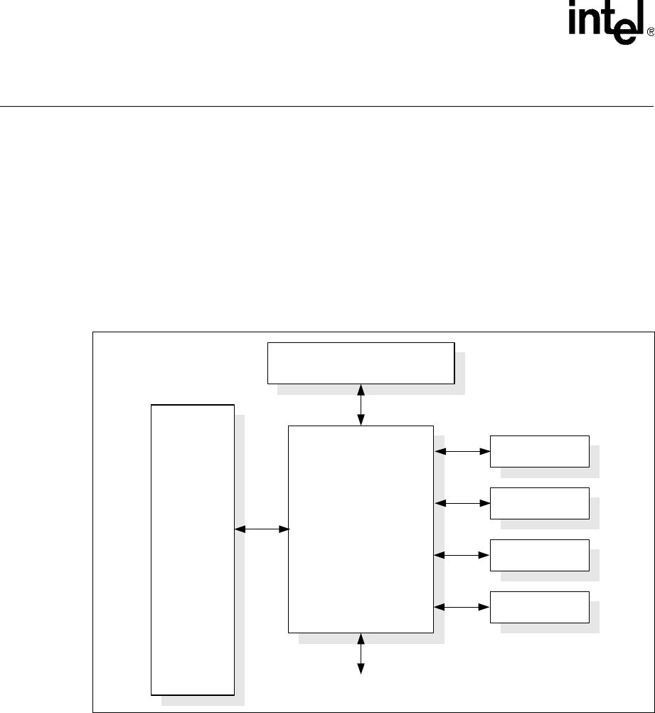
IXF1104 4-Port Gigabit Ethernet Media Access Controller
20 Datasheet
Document Number: 278757
Revision Number: 007
Revision Date: March 25, 2004
2.0 General Description
The IXF1104 provides up to a 4.0 Gbps interface to four individual 10/100/1000 Mbps full-duplex
or 10/100 Mbps half-duplex-capable Ethernet Media Access Controllers (MACs). The network
processor is supported through a System Packet Interface Phase 3 (SPI3) media interface. The
following PHY interfaces are selected on a per-port basis:
•Serializer/Deserializer (SerDes) with Optical Module Interface support
•Gigabit Media Independent Interface (GMII)
•Reduced Gigabit Media Independent Interface (RGMII).
Figure 1 illustrates the IXF1104 block diagram.
Figure 1. Block Diagram
Forwarding Engine/Network Processor
CPU
Intel
®
IXF1104 MAC
SerDes/RGMII/GMII Interface
MDIO
SPI3
uP IF
PHY 1 Device
PHY 2 Device
PHY 3 Device
PHY 4 Device
B3175-0
1

IXF1104 4-Port Gigabit Ethernet Media Access Controller
Datasheet 21
Document Number: 278757
Revision Number: 007
Revision Date: March 25, 2004
Figure 2 illustrates the IXF1104 internal architecture.
Figure 2. Internal Architecture
SPI3 Interface
CPU Interface RMON Statistics
Packet
TX
Buffer
RX
Packet
Buffer
Packet
Buffer
Packet
Buffer
Clock Control Block Clock Register Block
PLLs MDIO OMI
TX
TX
TX
RX
RX
RX
10/100/1000 MAC
10/100/1000 MAC
10/100/1000 MAC
10/100/1000 MAC
RGMII/GMII Interface
RGMII/GMII Interface
RGMII/GMII Interface
RGMII/GMII Interface
PMA Layer SerDes
PMA Layer SerDes
PMA Layer SerDes
PMA Layer SerDes
B3176-0
1
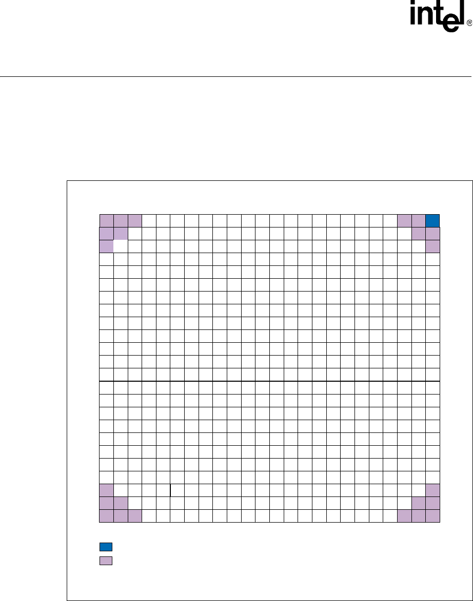
IXF1104 4-Port Gigabit Ethernet Media Access Controller
22 Datasheet
Document Number: 278757
Revision Number: 007
Revision Date: March 25, 2004
3.0 Ball Assignments and Ball List Tables
3.1 Ball Assignments
See Figure 3, Table 1 “Ball List in Alphanumeric Order by Signal Name” on page 23, and Table 2
“Ball List in Alphanumeric Order by Ball Location” on page 29 for the IXF1104 ball assignments.
Figure 3. Intel® IXF1104 552-Ball CBGA Assignments (Top View)
B1458-01
1
AD AC AB AA Y W V U T R P N M L K J H G F E D C B A
AD AC AB AA Y W V U T R P N M L K J H G F E D C B A
2
3
4
5
6
7
8
9
10
11
12
13
14
15
16
17
18
19
20
21
22
23
24
1
2
3
4
5
6
7
8
9
10
11
12
13
14
15
16
17
18
19
20
21
22
23
24
V7 U7 T7 R7 P7 N7 M7 L7 K7 J7 H7 G7 F7 E7 D7 G7 B7 A7
V8
V9
V10
V11
V12
V13
V14
V15
V16
V
17
V18
V19
V20
V21
V22
V23
V24
U8
U9
U10
U11
U12
U13
U14
U15
U16
U17
U18
U19
U20
U21
U22
U23
U24
T8
T9
T10
T11
T12
T13
T14
T15
T16
T17
T18
T19
T20
T21
T22
T23
T24
R8
R9
R10
R11
R12
R13
R14
R15
R16
R17
R18
R19
R20
R21
R22
R23
R24
P8
P9
P10
P11
P12
P13
P14
P15
P16
P17
P18
P19
P20
P21
P22
P23
P24
N8
N9
N10
N11
N12
N13
N14
N15
N16
N17
N18
N19
N20
N121
N22
N23
N24
M8
M9
M10
M11
M12
M13
M14
M15
M16
M17
M18
M19
M20
M21
M22
M23
M24
L8
L9
L10
L11
L12
L13
L14
L15
L16
L17
L18
L19
L20
L21
L22
L23
L24
K8
K9
K10
K11
K12
K13
K14
K15
K16
K17
K18
K19
K20
K21
K22
K23
K24
J8
J9
J10
J11
J12
J13
J14
J15
J16
J17
J18
J19
J20
J21
J22
J23
J24
H8
H9
H10
H11
H12
H13
H14
H15
H16
H17
H18
H19
H20
H21
H22
H23
H24
G8
G9
G10
G11
G12
G13
G14
G15
G16
G17
G18
G19
G20
G21
G22
G23
G24
F8
F9
F10
F11
F12
F13
F14
F15
F16
F17
F18
F19
F20
F21
F22
F23
F24
E8
E9
E10
E11
E12
E13
E14
E15
E16
E17
E18
E19
E20
E21
E22
E23
E24
D8
D9
D10
D11
D12
D13
D14
D15
D16
D17
D18
D19
D20
D21
D22
D23
D24
C8
C9
C10
C11
C12
C13
C14
C15
C16
C17
C18
C19
C20
C21
C22
C23
C24
B28
B9
B10
B11
B12
B13
B14
B15
B16
B17
B18
B19
B20
B21
B22
B23
B24
A8
A9
A10
A11
A12
A13
A14
A15
A16
A17
A18
A19
A20
A21
A22
A23
A24
= No Ball (A2, A3, A22, A23, A24, B1, B2, B23, B24, C1, C24, AB1, AB24, AC1, AC2, AC23, AC24, AD1, AD2, AD3,
AD22, AD23, AD24)
= No Pad (A1)
W24Y24AA24AB24AC24AD24
W23Y23AA23AB23AC23AD23
W22
Y22
AA22AB22AC22AD22
W21Y21AA21AB21AC21AD21
W20Y20AA20AB20AC20AD20
W19Y19AA19AB19AC19AD19
W18Y18AA18AB18AC18AD18
W17Y17AA17AB17AC17AD17
W16Y16AA16AB16AC16AD16
W15Y15AA15AB15AC15AD15
W14Y14AA14AB14AC14AD14
W13Y13AA13AB13AC13AD13
W12Y12AA12AB12AC12AD12
W11Y11AA11AB11AC11AD11
W10Y10AA10AB10AC10AD10
W9Y9AA9AB9AC9AD9
W8Y8AA8AB8AC8
AD8
W7Y7AA7AB7AC7AD7
A6B6C6D6F6F6G6H6J6K6L6M6N6P6R6T6U6V6W6Y6AA6AB6AC6AD6
A5B5C5D5E5F5G5H5J5K5L5M5N5P5R5T5U5V5W5Y5AA4AB5AC5AD5
A4B4C4D4E4F4G4H4J4K4L4M4N4P4R4T4U4V4W4Y4AA4AB4AC4AD4
A3B3C3D3E3F3G3H3J3K3L3M3N3P13R3T3U3V3W3Y3AA3AB3
AC3AD3
A2B2C2D2E2F2G2H2J2K2L2M2N2P2R2T2U2V2W2Y2AA2AB2AD2
B1C1D1E1F1G1H1J1K1L1M1N1P1R1T1U1V1W1Y1AA1AB1AC1
AC2
A1
AD1

IXF1104 4-Port Gigabit Ethernet Media Access Controller
23 Datasheet
Document Number: 278757
Revision Number: 007
Revision Date: March 25, 2004
3.2 Ball List Tables
3.2.1 Balls Listed in Alphabetic Order by Signal Name
Table 1 shows the ball locations and signal names arranged in alphanumeric order by signal name.
The following table notes relate to Table 1 and Table 2:
1. GMII Ball Connection:
See Table 16 for connection in RGMII or fiber mode.
2. SPI3 Ball Connection:
See Table 17 for proper SPHY and MPHY connection.
3. Fiber Mode Ball Connection:
See Table 16 for use in RGMII and GMII (copper mode).
Table 1. Ball List in Alphanumeric Order by Signal Name
Signal Name Ball
Location
AVDD1P8_1 A5
AVDD1P8_1 A20
AVDD1P8_2 T23
AVDD1P8_2 AB16
AVDD2P5_1 AD20
AVDD2P5_2 R18
AVDD2P5_2 U14
CLK125 AD19
COL_01AB6
COL_11AB10
COL_21AD15
COL_31AB17
CRS_01AA5
CRS_11AA9
CRS_21AB15
CRS_31AC16
DTPA_02D3
DTPA_12L1
DTPA_22A9
DTPA_32J7
GND B6
GND B10
GND B15
GND B19
GND D4
GND D8
GND D12
GND D13
GND D17
GND D21
GND F2
GND F6
GND F10
GND F15
GND F19
GND F23
GND H4
GND H8
GND H12
GND H13
GND H17
GND H21
GND J10
GND J15
GND K2
GND K6
GND K9
GND K11
Signal Name Ball
Location
GND K14
GND K16
GND K19
GND K23
GND L10
GND L12
GND L13
GND L15
GND M4
GND M8
GND M11
GND M14
GND M17
GND M21
GND N4
GND N8
GND N11
GND N14
GND N17
GND N21
GND P10
GND P12
GND P13
GND P15
Signal Name Ball
Location

IXF1104 4-Port Gigabit Ethernet Media Access Controller
Datasheet 24
Document Number: 278757
Revision Number: 007
Revision Date: March 25, 2004
GND R2
GND R6
GND R9
GND R11
GND R14
GND R16
GND R19
GND R23
GND T10
GND T15
GND U4
GND U8
GND U12
GND U13
GND U17
GND U21
GND W2
GND W6
GND W10
GND W15
GND W19
GND W23
GND AA4
GND AA8
GND AA12
GND AA13
GND AA17
GND AA21
GND AC6
GND AC10
GND AC15
GND AC19
GND AC14
GND L20
GND L5
GND R7
GND AB12
GND A4
Signal Name Ball
Location
GND A21
GND AD21
I2C_CLK L23
I2C_DATA_03L24
I2C_DATA_13M24
I2C_DATA_23N24
I2C_DATA_33P24
LED_CLK K24
LED_DATA M22
LED_LATCH L22
MDC4W24
MDIO4V21
MOD_DEF_INT N22
NC D24
NC E12
NC F11
NC G15
NC H7
NC H18
NC J21
NC K7
NC K18
NC K20
NC K22
NC L18
NC L19
NC L21
NC M7
NC M18
NC M20
NC N3
NC N18
NC P2
NC P4
NC P6
NC P7
NC P8
NC P17
Signal Name Ball
Location
NC P18
NC R5
NC R10
NC R12
NC R13
NC R15
NC R20
NC T6
NC T7
NC T8
NC T9
NC T21
NC T22
NC U5
NC U7
NC U9
NC U11
NC U18
NC V9
NC V10
NC V11
NC V13
NC AB18
NC AD4
NC AD5
No Ball A2
No Ball A3
No Ball A22
No Ball A23
No Ball A24
No Ball B1
No Ball B2
No Ball B23
No Ball B24
No Ball C1
No Ball C24
No Ball AB1
No Ball AB24
Signal Name Ball
Location

IXF1104 4-Port Gigabit Ethernet Media Access Controller
25 Datasheet
Document Number: 278757
Revision Number: 007
Revision Date: March 25, 2004
No Ball AC1
No Ball AC2
No Ball AC23
No Ball AC24
No Ball AD1
No Ball AD2
No Ball AD3
No Ball AD22
No Ball AD23
No Ball AD24
No Pad A1
PTPA2B11
RDAT_02A15
RDAT_12A14
RDAT_22B14
RDAT_32C14
RDAT_42C13
RDAT_52D14
RDAT_62E14
RDAT_72F14
RDAT_82A17
RDAT_92C17
RDAT_102D16
RDAT_112E16
RDAT_122F16
RDAT_132E17
RDAT_142E18
RDAT_152F18
RDAT_162B20
RDAT_172B22
RDAT_182C20
RDAT_192C21
RDAT_202C22
RDAT_212D22
RDAT_222E22
RDAT_232E21
RDAT_242G18
RDAT_252G19
Signal Name Ball
Location
RDAT_262G20
RDAT_272G21
RDAT_282G22
RDAT_292G23
RDAT_302G24
RDAT_312F24
RENB_02A13
RENB_12A18
RENB_22C19
RENB_32E24
REOP_02C16
REOP_12D18
REOP_22C23
REOP_32J19
RERR_02A16
RERR_12G17
RERR_22D20
RERR_32H20
RFCLK2A19
RMOD02G14
RMOD12G13
RPRTY_02E15
RPRTY_12G16
RPRTY_22E20
RPRTY_32F20
RSOP_02B16
RSOP_12C18
RSOP_22E23
RSOP_32J18
RSX2E13
RVAL_02C15
RVAL_12B18
RVAL_22E19
RVAL_32F22
RX_DV_01V5
RX_DV_11AB11
RX_DV_21Y24
RX_DV_31V18
Signal Name Ball
Location
RX_ER_01W5
RX_ER_11Y12
RX_ER_21AA22
RX_ER_31U20
RX_LOS_INT3P19
RX_N_03R22
RX_N_13U22
RX_N_23R24
RX_N_33V24
RX_P_03P22
RX_P_13V22
RX_P_23T24
RX_P_33U24
RXC_01V4
RXC_11AD11
RXC_21AA24
RXC_31V23
RXD0_01V8
RXD0_11Y9
RXD0_21Y20
RXD0_31Y17
RXD1_01V7
RXD1_11Y11
RXD1_21Y21
RXD1_31Y18
RXD2_01W7
RXD2_11W11
RXD2_21Y22
RXD2_31Y19
RXD3_01Y7
RXD3_11W9
RXD3_21Y23
RXD3_31W18
RXD4_01Y6
RXD4_11AD10
RXD4_21W22
RXD4_31T16
RXD5_01Y5
Signal Name Ball
Location

IXF1104 4-Port Gigabit Ethernet Media Access Controller
Datasheet 26
Document Number: 278757
Revision Number: 007
Revision Date: March 25, 2004
RXD5_11AC11
RXD5_21V20
RXD5_31T17
RXD6_01AB5
RXD6_11AA11
RXD6_21V19
RXD6_31T18
RXD7_01AC5
RXD7_11Y10
RXD7_21W20
RXD7_31T19
STPA2C11
SYS_RST_L AD12
TADR02A11
TADR12A12
TCLK J22
TDAT02B3
TDAT12C2
TDAT22C3
TDAT32D1
TDAT42C4
TDAT52C5
TDAT62B5
TDAT72C6
TDAT82F1
TDAT92G1
TDAT102G2
TDAT112H1
TDAT122J1
TDAT132J2
TDAT142J3
TDAT152H3
TDAT162E5
TDAT172E6
TDAT182E7
TDAT192E8
TDAT202E9
TDAT212E10
Signal Name Ball
Location
TDAT222F9
TDAT232C8
TDAT242G4
TDAT252G5
TDAT262G6
TDAT272G7
TDAT282G8
TDAT292G9
TDAT302F5
TDAT312F7
TDI J24
TDO H24
TENB_02B7
TENB_12E2
TENB_22C9
TENB_32J4
TEOP_02A7
TEOP_12F3
TEOP_22E4
TEOP_32H5
TERR_02A8
TERR_12K1
TERR_22E11
TERR_32J8
TFCLK2D7
TMOD02A6
TMOD12D9
TMS H22
TPRTY_02D5
TPRTY_12G3
TPRTY_22B9
TPRTY_32J6
TRST_L J23
TSOP_02C7
TSOP_12E3
TSOP_22C10
TSOP_32J5
TSX E1
Signal Name Ball
Location
TX_EN_01AB2
TX_EN_11Y8
TX_EN_21AC22
TX_EN_31V12
TX_ER_01W1
TX_ER_11AD6
TX_ER_21AD17
TX_ER_31AB13
TX_FAULT_INT3P23
TX_N_03Y14
TX_N_13AD14
TX_N_23Y16
TX_N_33AD18
TX_P_03Y13
TX_P_13AD13
TX_P_23W16
TX_P_33AC18
TXC_01AA1
TXC_11AD7
TXC_21AC20
TXC_31AB14
TXD0_01Y1
TXD0_11AC7
TXD0_21AB20
TXD0_31V14
TXD1_01Y2
TXD1_11AB7
TXD1_21AB21
TXD1_31V15
TXD2_01Y3
TXD2_11AB9
TXD2_21AB22
TXD2_31V16
TXD3_01AA3
TXD3_11AD9
TXD3_21AB23
TXD3_31V17
TXD4_01AB3
Signal Name Ball
Location

IXF1104 4-Port Gigabit Ethernet Media Access Controller
27 Datasheet
Document Number: 278757
Revision Number: 007
Revision Date: March 25, 2004
TXD4_11AA7
TXD4_21AD16
TXD4_31AA14
TXD5_01AC3
TXD5_11AB8
TXD5_21AB19
TXD5_31Y15
TXD6_01AB4
TXD6_11AD8
TXD6_21AA20
TXD6_31AA16
TXD7_01Y4
TXD7_11AC9
TXD7_21AA18
TXD7_31W14
TXPAUSE_ADD0 N20
TXPAUSE_ADD1 P20
TXPAUSE_ADD2 P21
TXPAUSEFR T20
UPX_ADD0 P3
UPX_ADD1 N1
UPX_ADD2 P1
UPX_ADD3 R1
UPX_ADD4 T1
UPX_ADD5 U1
UPX_ADD6 V1
UPX_ADD7 V2
UPX_ADD8 V3
UPX_ADD9 U3
UPX_ADD10 T3
UPX_BADD0 T2
UPX_BADD1 W3
UPX_CS_L R3
UPX_DATA0 L2
UPX_DATA1 K3
UPX_DATA2 L3
UPX_DATA3 M3
UPX_DATA4 L4
Signal Name Ball
Location
UPX_DATA5 N5
UPX_DATA6 M5
UPX_DATA7 K5
UPX_DATA8 P5
UPX_DATA9 L6
UPX_DATA10 L7
UPX_DATA11 N7
UPX_DATA12 L8
UPX_DATA13 H9
UPX_DATA14 J9
UPX_DATA15 N10
UPX_DATA16 M10
UPX_DATA17 K10
UPX_DATA18 G10
UPX_DATA19 H11
UPX_DATA20 G11
UPX_DATA21 K12
UPX_DATA22 G12
UPX_DATA23 K13
UPX_DATA24 H14
UPX_DATA25 K15
UPX_DATA26 N15
UPX_DATA27 M15
UPX_DATA28 J16
UPX_DATA29 H16
UPX_DATA30 J17
UPX_DATA31 L17
UPX_RD_L V6
UPX_RDY_L M1
UPX_WIDTH0 U16
UPX_WIDTH1 T5
UPX_WR_L T4
VDD D6
VDD D10
VDD D15
VDD D19
VDD F4
VDD F21
Signal Name Ball
Location
VDD H10
VDD H15
VDD J11
VDD J14
VDD K4
VDD K8
VDD K17
VDD K21
VDD L9
VDD L11
VDD L14
VDD L16
VDD P9
VDD P11
VDD P14
VDD P16
VDD R4
VDD R8
VDD R17
VDD R21
VDD T11
VDD T14
VDD U10
VDD U15
VDD W4
VDD W21
VDD AA6
VDD AA10
VDD AA15
VDD AA19
VDD C12
VDD D11
VDD J20
VDD A10
VDD2 B4
VDD2 B8
VDD2 B12
VDD2 D2
Signal Name Ball
Location

IXF1104 4-Port Gigabit Ethernet Media Access Controller
Datasheet 28
Document Number: 278757
Revision Number: 007
Revision Date: March 25, 2004
VDD2 F8
VDD2 F12
VDD2 H2
VDD2 H6
VDD2 J12
VDD2 M2
VDD2 M6
VDD2 M9
VDD2 M12
VDD3 B13
VDD3 B17
VDD3 B21
VDD3 D23
VDD3 F13
VDD3 F17
VDD3 H19
VDD3 H23
VDD3 J13
VDD3 M13
VDD3 M16
VDD3 M19
VDD3 M23
VDD4 N13
VDD4 N16
VDD4 N19
VDD4 N23
VDD4 T13
VDD4 U19
VDD4 U23
VDD4 W13
VDD4 W17
VDD4 AA23
VDD4 AC13
VDD4 AC17
VDD4 AC21
VDD5 N2
VDD5 N6
VDD5 N9
Signal Name Ball
Location
VDD5 N12
VDD5 T12
VDD5 U2
VDD5 U6
VDD5 W8
VDD5 W12
VDD5 AA2
VDD5 AC4
VDD5 AC8
VDD5 AC12
Signal Name Ball
Location

IXF1104 4-Port Gigabit Ethernet Media Access Controller
29 Datasheet
Document Number: 278757
Revision Number: 007
Revision Date: March 25, 2004
3.2.2 Balls Listed in Alphabetic Order by Ball Location
Table 2 shows the ball locations and signal names arranged in order by ball location.
Table 2. Ball List in Alphanumeric Order by Ball Location
Ball
Location Signal Name
A1 No Pad
A2 No Ball
A3 No Ball
A4 GND
A5 AVDD1P8_1
A6 TMOD02
A7 TEOP_02
A8 TERR_02
A9 DTPA_22
A10 VDD
A11 TADR02
A12 TADR12
A13 RENB_02
A14 RDAT_12
A15 RDAT_02
A16 RERR_02
A17 RDAT_82
A18 RENB_12
A19 RFCLK2
A20 AVDD1P8_1
A21 GND
A22 No Ball
A23 No Ball
A24 No Ball
B1 No Ball
B2 No Ball
B3 TDAT02
B4 VDD2
B5 TDAT62
B6 GND
B7 TENB_02
B8 VDD2
B9 TPRTY_22
B10 GND
B11 PTPA2
B12 VDD2
B13 VDD3
B14 RDAT_22
B15 GND
B16 RSOP_02
B17 VDD3
B18 RVAL_12
B19 GND
B20 RDAT_162
B21 VDD3
B22 RDAT_172
B23 No Ball
B24 No Ball
C1 No Ball
C2 TDAT12
C3 TDAT22
C4 TDAT42
C5 TDAT52
C6 TDAT72
C7 TSOP_02
C8 TDAT232
C9 TENB_22
C10 TSOP_22
C11 STPA2
C12 VDD
C13 RDAT_42
C14 RDAT_32
C15 RVAL_02
C16 REOP_02
C17 RDAT_92
C18 RSOP_12
C19 RENB_22
Ball
Location Signal Name
C20 RDAT_182
C21 RDAT_192
C22 RDAT_202
C23 REOP_22
C24 No Ball
D1 TDAT32
D2 VDD2
D3 DTPA_02
D4 GND
D5 TPRTY_02
D6 VDD
D7 TFCLK2
D8 GND
D9 TMOD12
D10 VDD
D11 VDD
D12 GND
D13 GND
D14 RDAT_52
D15 VDD
D16 RDAT_102
D17 GND
D18 REOP_12
D19 VDD
D20 RERR_22
D21 GND
D22 RDAT_212
D23 VDD3
D24 NC
E1 TSX
E2 TENB_12
E3 TSOP_12
E4 TEOP_22
E5 TDAT162
Ball
Location Signal Name

IXF1104 4-Port Gigabit Ethernet Media Access Controller
Datasheet 30
Document Number: 278757
Revision Number: 007
Revision Date: March 25, 2004
E6 TDAT172
E7 TDAT182
E8 TDAT192
E9 TDAT202
E10 TDAT212
E11 TERR_22
E12 NC
E13 RSX2
E14 RDAT_62
E15 RPRTY_02
E16 RDAT_112
E17 RDAT_132
E18 RDAT_142
E19 RVAL_22
E20 RPRTY_22
E21 RDAT_232
E22 RDAT_222
E23 RSOP_22
E24 RENB_32
F1 TDAT82
F2 GND
F3 TEOP_12
F4 VDD
F5 TDAT302
F6 GND
F7 TDAT312
F8 VDD2
F9 TDAT222
F10 GND
F11 NC
F12 VDD2
F13 VDD3
F14 RDAT_72
F15 GND
F16 RDAT_122
F17 VDD3
F18 RDAT_152
F19 GND
Ball
Location Signal Name
F20 RPRTY_32
F21 VDD
F22 RVAL_32
F23 GND
F24 RDAT_312
G1 TDAT92
G2 TDAT102
G3 TPRTY_12
G4 TDAT242
G5 TDAT252
G6 TDAT262
G7 TDAT272
G8 TDAT282
G9 TDAT292
G10 UPX_DATA18
G11 UPX_DATA20
G12 UPX_DATA22
G13 RMOD12
G14 RMOD02
G15 NC
G16 RPRTY_12
G17 RERR_12
G18 RDAT_242
G19 RDAT_252
G20 RDAT_262
G21 RDAT_272
G22 RDAT_282
G23 RDAT_292
G24 RDAT_302
H1 TDAT112
H2 VDD2
H3 TDAT152
H4 GND
H5 TEOP_32
H6 VDD2
H7 NC
H8 GND
H9 UPX_DATA13
Ball
Location Signal Name
H10 VDD
H11 UPX_DATA19
H12 GND
H13 GND
H14 UPX_DATA24
H15 VDD
H16 UPX_DATA29
H17 GND
H18 NC
H19 VDD3
H20 RERR_32
H21 GND
H22 TMS
H23 VDD3
H24 TDO
J1 TDAT122
J2 TDAT132
J3 TDAT142
J4 TENB_32
J5 TSOP_32
J6 TPRTY_32
J7 DTPA_32
J8 TERR_32
J9 UPX_DATA14
J10 GND
J11 VDD
J12 VDD2
J13 VDD3
J14 VDD
J15 GND
J16 UPX_DATA28
J17 UPX_DATA30
J18 RSOP_32
J19 REOP_32
J20 VDD
J21 NC
J22 TCLK
J23 TRST_L
Ball
Location Signal Name

IXF1104 4-Port Gigabit Ethernet Media Access Controller
31 Datasheet
Document Number: 278757
Revision Number: 007
Revision Date: March 25, 2004
J24 TDI
K1 TERR_12
K2 GND
K3 UPX_DATA1
K4 VDD
K5 UPX_DATA7
K6 GND
K7 NC
K8 VDD
K9 GND
K10 UPX_DATA17
K11 GND
K12 UPX_DATA21
K13 UPX_DATA23
K14 GND
K15 UPX_DATA25
K16 GND
K17 VDD
K18 NC
K19 GND
K20 NC
K21 VDD
K22 NC
K23 GND
K24 LED_CLK
L1 DTPA_12
L2 UPX_DATA0
L3 UPX_DATA2
L4 UPX_DATA4
L5 GND
L6 UPX_DATA9
L7 UPX_DATA10
L8 UPX_DATA12
L9 VDD
L10 GND
L11 VDD
L12 GND
L13 GND
Ball
Location Signal Name
L14 VDD
L15 GND
L16 VDD
L17 UPX_DATA31
L18 NC
L19 NC
L20 GND
L21 NC
L22 LED_LATCH
L23 I2C_CLK
L24 I2C_DATA_03
M1 UPX_RDY_L
M2 VDD2
M3 UPX_DATA3
M4 GND
M5 UPX_DATA6
M6 VDD2
M7 NC
M8 GND
M9 VDD2
M10 UPX_DATA16
M11 GND
M12 VDD2
M13 VDD3
M14 GND
M15 UPX_DATA27
M16 VDD3
M17 GND
M18 NC
M19 VDD3
M20 NC
M21 GND
M22 LED_DATA
M23 VDD3
M24 I2C_DATA_13
N1 UPX_ADD1
N2 VDD5
N3 NC
Ball
Location Signal Name
N4 GND
N5 UPX_DATA5
N6 VDD5
N7 UPX_DATA11
N8 GND
N9 VDD5
N10 UPX_DATA15
N11 GND
N12 VDD5
N13 VDD4
N14 GND
N15 UPX_DATA26
N16 VDD4
N17 GND
N18 NC
N19 VDD4
N20 TXPAUSE_ADD0
N21 GND
N22 MOD_DEF_INT
N23 VDD4
N24 I2C_DATA_23
P1 UPX_ADD2
P2 NC
P3 UPX_ADD0
P4 NC
P5 UPX_DATA8
P6 NC
P7 NC
P8 NC
P9 VDD
P10 GND
P11 VDD
P12 GND
P13 GND
P14 VDD
P15 GND
P16 VDD
P17 NC
Ball
Location Signal Name

IXF1104 4-Port Gigabit Ethernet Media Access Controller
Datasheet 32
Document Number: 278757
Revision Number: 007
Revision Date: March 25, 2004
P18 NC
P19 RX_LOS_INT3
P20 TXPAUSE_ADD1
P21 TXPAUSE_ADD2
P22 RX_P_03
P23 TX_FAULT_INT3
P24 I2C_DATA_33
R1 UPX_ADD3
R2 GND
R3 UPX_CS_L
R4 VDD
R5 NC
R6 GND
R7 GND
R8 VDD
R9 GND
R10 NC
R11 GND
R12 NC
R13 NC
R14 GND
R15 NC
R16 GND
R17 VDD
R18 AVDD2P5_2
R19 GND
R20 NC
R21 VDD
R22 RX_N_03
R23 GND
R24 RX_N_23
T1 UPX_ADD4
T2 UPX_BADD0
T3 UPX_ADD10
T4 UPX_WR_L
T5 UPX_WIDTH1
T6 NC
T7 NC
Ball
Location Signal Name
T8 NC
T9 NC
T10 GND
T11 VDD
T12 VDD5
T13 VDD4
T14 VDD
T15 GND
T16 RXD4_31
T17 RXD5_31
T18 RXD6_31
T19 RXD7_31
T20 TXPAUSEFR
T21 NC
T22 NC
T23 AVDD1P8_2
T24 RX_P_23
U1 UPX_ADD5
U2 VDD5
U3 UPX_ADD9
U4 GND
U5 NC
U6 VDD5
U7 NC
U8 GND
U9 NC
U10 VDD
U11 NC
U12 GND
U13 GND
U14 AVDD2P5_2
U15 VDD
U16 UPX_WIDTH0
U17 GND
U18 NC
U19 VDD4
U20 RX_ER_31
U21 GND
Ball
Location Signal Name
U22 RX_N_13
U23 VDD4
U24 RX_P_33
V1 UPX_ADD6
V2 UPX_ADD7
V3 UPX_ADD8
V4 RXC_01
V5 RX_DV_01
V6 UPX_RD_L
V7 RXD1_01
V8 RXD0_01
V9 NC
V10 NC
V11 NC
V12 TX_EN_31
V13 NC
V14 TXD0_31
V15 TXD1_31
V16 TXD2_31
V17 TXD3_31
V18 RX_DV_31
V19 RXD6_21
V20 RXD5_21
V21 MDIO4
V22 RX_P_13
V23 RXC_31
V24 RX_N_33
W1 TX_ER_01
W2 GND
W3 UPX_BADD1
W4 VDD
W5 RX_ER_01
W6 GND
W7 RXD2_01
W8 VDD5
W9 RXD3_11
W10 GND
W11 RXD2_11
Ball
Location Signal Name

IXF1104 4-Port Gigabit Ethernet Media Access Controller
33 Datasheet
Document Number: 278757
Revision Number: 007
Revision Date: March 25, 2004
W12 VDD5
W13 VDD4
W14 TXD7_31
W15 GND
W16 TX_P_23
W17 VDD4
W18 RXD3_31
W19 GND
W20 RXD7_21
W21 VDD
W22 RXD4_21
W23 GND
W24 MDC4
Y1 TXD0_01
Y2 TXD1_01
Y3 TXD2_01
Y4 TXD7_01
Y5 RXD5_01
Y6 RXD4_01
Y7 RXD3_01
Y8 TX_EN_11
Y9 RXD0_11
Y10 RXD7_11
Y11 RXD1_11
Y12 RX_ER_11
Y13 TX_P_03
Y14 TX_N_03
Y15 TXD5_31
Y16 TX_N_23
Y17 RXD0_31
Y18 RXD1_31
Y19 RXD2_31
Y20 RXD0_21
Y21 RXD1_21
Y22 RXD2_21
Y23 RXD3_21
Y24 RX_DV_21
AA1 TXC_01
Ball
Location Signal Name
AA2 VDD5
AA3 TXD3_01
AA4 GND
AA5 CRS_01
AA6 VDD
AA7 TXD4_11
AA8 GND
AA9 CRS_11
AA10 VDD
AA11 RXD6_11
AA12 GND
AA13 GND
AA14 TXD4_31
AA15 VDD
AA16 TXD6_31
AA17 GND
AA18 TXD7_21
AA19 VDD
AA20 TXD6_21
AA21 GND
AA22 RX_ER_21
AA23 VDD4
AA24 RXC_21
AB1 No Ball
AB2 TX_EN_01
AB3 TXD4_01
AB4 TXD6_01
AB5 RXD6_01
AB6 COL_01
AB7 TXD1_11
AB8 TXD5_11
AB9 TXD2_11
AB10 COL_11
AB11 RX_DV_11
AB12 GND
AB13 TX_ER_31
AB14 TXC_31
AB15 CRS_21
Ball
Location Signal Name
AB16 AVDD1P8_2
AB17 COL_31
AB18 NC
AB19 TXD5_21
AB20 TXD0_21
AB21 TXD1_21
AB22 TXD2_21
AB23 TXD3_21
AB24 No Ball
AC1 No Ball
AC2 No Ball
AC3 TXD5_01
AC4 VDD5
AC5 RXD7_01
AC6 GND
AC7 TXD0_11
AC8 VDD5
AC9 TXD7_11
AC10 GND
AC11 RXD5_11
AC12 VDD5
AC13 VDD4
AC14 GND
AC15 GND
AC16 CRS_31
AC17 VDD4
AC18 TX_P_33
AC19 GND
AC20 TXC_21
AC21 VDD4
AC22 TX_EN_21
AC23 No Ball
AC24 No Ball
AD1 No Ball
AD2 No Ball
AD3 No Ball
AD4 NC
AD5 NC
Ball
Location Signal Name

IXF1104 4-Port Gigabit Ethernet Media Access Controller
Datasheet 34
Document Number: 278757
Revision Number: 007
Revision Date: March 25, 2004
AD6 TX_ER_11
AD7 TXC_11
AD8 TXD6_11
AD9 TXD3_11
AD10 RXD4_11
AD11 RXC_11
AD12 SYS_RST_L
AD13 TX_P_13
AD14 TX_N_13
AD15 COL_21
AD16 TXD4_21
AD17 TX_ER_21
AD18 TX_N_33
AD19 CLK125
AD20 AVDD2P5_1
AD21 GND
AD22 No Ball
AD23 No Ball
AD24 No Ball
Ball
Location Signal Name

IXF1104 4-Port Gigabit Ethernet Media Access Controller
35 Datasheet
Document Number: 278757
Revision Number: 007
Revision Date: March 25, 2004

IXF1104 4-Port Gigabit Ethernet Media Access Controller
36 Datasheet
Document Number: 278757
Revision Number: 007
Revision Date: March 25, 2004
4.0 Ball Assignments and Signal Descriptions
4.1 Naming Conventions
4.1.1 Signal Name Conventions
Signal names begin with a Signal Mnemonic, and can also contain one or more of the following
designations: a differential pair designation, a serial designation, a port designation (RGMII
interface), and an active low designation. Signal naming conventions are as follows:
Differential Pair + Port Designation. The positive and negative components of differential pairs
tied to a specific port are designated by the Signal Mnemonic, immediately followed by an
underscore and either P (positive component) or N (negative component), and an underscore
followed by the port designation. For example, SerDes interface signals for port 0 are identified as
TX_P_0 and TX_N_0.
Serial Designation. A set of signals that are not tied to any specific port are designated by the
Signal Mnemonic, followed by a bracketed serial designation. For example, the set of 11 CPU
Address Bus signals is identified as UPX_ADD[10:0].
Port Designation. Individual signals that apply to a particular port are designated by the Signal
Mnemonic, immediately followed by an underscore and the Port Designation. For example,
RGMII Transmit Control signals are identified as TX_CTL_0, TX_CTL_1, TX_CTL_2, and so on.
Port Bus Designation. A set of bus signals that apply to a particular port are designated by the
Signal Mnemonic, immediately followed by a bracketed bus designation, followed by an
underscore and the port designation. For example, RGMII transmit data bus signals are identified
as TD[3:0]_0, TD[3:0]_1, TD[3:0]_2, and so on.
Active Low Designation. A control input or indicator output that is active Low is designated by a
final suffix consisting of an underscore followed by an upper case “L”. For example, the CPU cycle
complete identifier is shown as UPX_RDY_L.
4.1.2 Register Address Conventions
Registers located in on-chip memory are accessed using a register address, which is provided in
Hex notation. A Register Address is indicated by the dollar sign ($), followed by the memory
location in Hex.
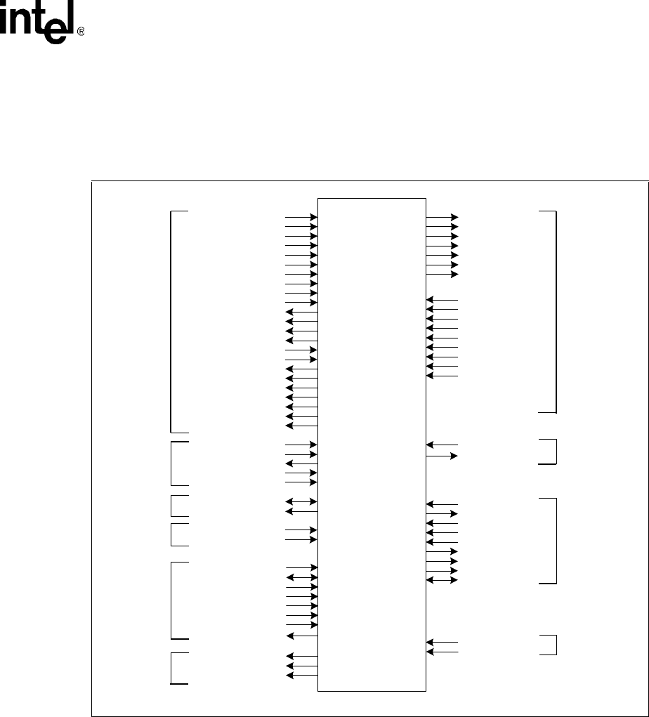
IXF1104 4-Port Gigabit Ethernet Media Access Controller
Datasheet 37
Document Number: 278757
Revision Number: 007
Revision Date: March 25, 2004
4.2 Interface Signal Groups
This section describes the IXF1104 signals in groups according to the associated interface or
function. Figure 4 shows the various interfaces available on the IXF1104.
Figure 4. Interface Signals
T D AT [ 31:0]
TFCLK
TENB_0
TERR_0
TPRTY_0
TMOD[1:0]
TSX
TSOP_0
TEOP_0
TADR[1:0]
DTPA_0:3
STPA
PTPA
R D AT[ 31: 0]
RFCLK
RENB_0
RVAL_0
RERR_0
RPRTY_0
RMOD[1:0]
RSX
RSOP_0
REOP_0
TMS
TDI
TDO
TCLK
MDIO
MDC
TXPAU SEADD [2:0]
TXPAUSEFR
UPX_WIDTH[1:0]
U PX_D AT A[ 31: 0]
U PX_AD D [10:0]
U PX_BAD D [1: 0]
UPX_WR_L
UPX_RD_L
UPX_CS_L
U PX_R D Y_L
LED_CLK
LED_DATA
LED _LAT C H
SYS_R ES_L
CLK125
MOD _DEF_0:3
TX_D I SABLE_0:3
T X_F AU LT _0: 3
RX_LOS_0:3
TX_F AU LT _IN T
R X_LOS_IN T
MOD _DEF_IN T
I
2
C_CLK
I
2
C_DATA_0:3
SPI3
Interface
JTA G
Interface
MDIO
Interface
Pause
Control
Interface
CPU
Interface
LED
Interface
System
In terf ace
GMII RGMII
GMII and
RGMII
In terf aces*
* D at a and clock balls are shared f or
GMII and RGMII Interfaces
SerDes
In terf ace
Optical
Module
In terf ace
Si g n als*
*
** These optical module signals
are mult iplexed on the GMII balls.
RX_P/N_0:3
TX_P/N_0:3
TRST_L
Intel
®
IXF1104
Media Access
Controller
B3181-01
MPHYSPHY
TFCLK
TE NB _0: 3
TE RR _0: 3
T PR T Y_0: 3
TSOP_0:3
TEOP_0:3
TDAT[7:0]_0:3
TADR[1:0]
D T PA _0: 3
PTPA
RDAT[7:0]_0:3
RFCLK
RENB_0:3
R VAL_0: 3
RERR_0:3
RPRTY_0:3
R SOP _0: 3
R EOP _0: 3
TXC_0:3
TX D[ 7: 0] _3
T XC _0: 3
TD[3:0]_3
TX D[ 7: 0] _2 T D [3:0] _2
TX D[ 7: 0] _1 T D [3:0] _1
TX D[ 7: 0] _0 TD[3:0]_0
TX_EN_0:3
TX_ER_0:3
T X_C T L_0: 3
R XC _0: 3 R XC _0: 3
RXD[7:0]_3
RD[3:0]_3
RXD[7:0]_2
RD[3:0]_2RXD[7:0]_1
RD[3:0]_1
RXD[7:0]_0
RD[3:0]_0
R X_D V_0:3
RX_ER_0:3
CRS_0:3
CO L_0:3
R X_C T L_0: 3

IXF1104 4-Port Gigabit Ethernet Media Access Controller
38 Datasheet
Document Number: 278757
Revision Number: 007
Revision Date: March 25, 2004
4.3 Signal Description Tables
The I/O signals, power supplies, or ground returns associated with each IXF1104 connection ball
are described in Table 3 through Table 14.
Table 3. SPI3 Interface Signal Descriptions (Sheet 1 of 8)
Signal Name Ball
Designator Type Standard Description
MPHY SPHY
TDAT31
TDAT30
TDAT29
TDAT28
TDAT27
TDAT26
TDAT25
TDAT24
TDAT7_3
TDAT6_3
TDAT5_3
TDAT4_3
TDAT3_3
TDAT2_3
TDAT1_3
TDAT0_3
F7
F5
G9
G8
G7
G6
G5
G4
Input 3.3 V
LVTTL
Transmit Data Bus.
Carries payload data to the IXF1104 egress
path.
Mode
32-bit Multi-PHY
4 x 8 Single-PHY
Bits
[31:24]
[7:0] for port 3
TDAT23
TDAT22
TDAT21
TDAT20
TDAT19
TDAT18
TDAT17
TDAT16
TDAT7_2
TDAT6_2
TDAT5_2
TDAT4_2
TDAT3_2
TDAT2_2
TDAT1_2
TDAT0_2
C8
F9
E10
E9
E8
E7
E6
E5
Input 3.3 V
LVTTL
Transmit Data Bus.
Carries payload data to the IXF1104 egress
path.
Mode
32-bit Multi-PHY
4 x 8 Single-PHY
Bits
[23:16]
[7:0] for port 2
TDAT15
TDAT14
TDAT13
TDAT12
TDAT11
TDAT10
TDAT9
TDAT8
TDAT7_1
TDAT6_1
TDAT5_1
TDAT4_1
TDAT3_1
TDAT2_1
TDAT1_1
TDAT0_1
H3
J3
J2
J1
H1
G2
G1
F1
Input 3.3 V
LVTTL
Transmit Data Bus.
Carries payload data to the IXF1104 egress
path.
Mode
32-bit Multi-PHY
4 x 8 Single-PHY
Bits
[15:8]
[7:0] for port 1
TDAT7
TDAT6
TDAT5
TDAT4
TDAT3
TDAT2
TDAT1
TDAT0
TDAT7_0
TDAT6_0
TDAT5_0
TDAT4_0
TDAT3_0
TDAT2_0
TDAT1_0
TDAT0_0
C6
B5
C5
C4
D1
C3
C2
B3
Input 3.3 V
LVTTL
Transmit Data Bus.
Carries payload data to the IXF1104 egress
path.
Mode
32-bit Multi-PHY
4 x 8 Single-PHY
Bits
7:0]
[7:0] for port 0
TFCLK TFCLK D7 Input 3.3 V
LVTTL
Transmit Clock.
TFCLK is the clock associated with all
transmit signals. Data and control lines are
sampled on the rising edge of TFCLK
(frequency operation range 90 - 133 MHz).

IXF1104 4-Port Gigabit Ethernet Media Access Controller
Datasheet 39
Document Number: 278757
Revision Number: 007
Revision Date: March 25, 2004
TPRTY_0 TPRTY_0
TPRTY_1
TPRTY_2
TPRTY_3
D5
G3
B9
J6
Input 3.3 V
LVTTL
Transmit Parity.
TPRTY indicates odd parity for the TDAT
bus. TPRTY is valid only when a channel
asserts either TENB or TSX. Odd parity is
the default configuration; however, even
parity can be selected (see Table 146 “SPI3
Transmit and Global Configuration
($0x700)” on page 212).
32-bit Multi-PHY mode: TPRTY_0 is the
parity bit covering all 32 bits.
4 x 8 Single-PHY mode: TPRTY_0:3 bits
correspond to the respective TDAT[3:0]_n
channels.
TENB_0 TENB_0
TENB_1
TENB_2
TENB_3
B7
E2
C9
J4
Input 3.3 V
LVTTL
Transmit Write Enable.
TENB_0:3 asserted causes an attached
PHY to process TDAT[n], TMOD, TSOP,
TEOP and TERR signals.
32-bit Multi-PHY mode: TENB_0 is the
enable bit for all 32 bits.
4 x 8 Single-PHY mode: TENB_0:3 bits
correspond to the respective TDAT[3:0]_n
channels and their associated control and
status signals.
TERR_0 TERR_0
TERR_1
TERR_2
TERR_3
A8
K1
E11
J8
Input 3.3 V
LVTTL
Transmit Error.
TERR indicates that there is an error in the
current packet. TERR is valid when
simultaneously asserted with TEOP and
TENB.
32-bit Multi-PHY mode: TERR_0 is the bit
asserted for all 32 bits.
4 x 8 Single-PHY mode: Each bit of
TERR_0:3 corresponds to the respective
TDAT[3:0]_n channel.
TSOP_0 TSOP_0
TSOP_1
TSOP_2
TSOP_3
C7
E3
C10
J5
Input 3.3 V
LVTTL
Transmit Start-of-Packet.
TSOP indicates the start of a packet and is
valid when asserted simultaneously with
TENB.
32-bit Multi-PHY mode: TSOP_0 is the bit
asserted for all 32 bits.
4 x 8 Single-PHY mode: Each bit of
TSOP_0:3 corresponds to the respective
TDAT[3:0]_n channel.
TEOP_0 TEOP_0
TEOP_1
TEOP_2
TEOP_3
A7
F3
E4
H5
Input 3.3 V
LVTTL
Transmit End-of-Packet.
TEOP indicates the end of a packet and is
valid when asserted simultaneously with
TENB.
32-bit Multi-PHY mode: TEOP_0 is the bit
asserted for all 32 bits.
4 x 8 Single-PHY mode: Each bit of
TEOP_0:3 corresponds to the respective
TDAT[3:0]_n channel.
Table 3. SPI3 Interface Signal Descriptions (Sheet 2 of 8)
Signal Name Ball
Designator Type Standard Description
MPHY SPHY

IXF1104 4-Port Gigabit Ethernet Media Access Controller
40 Datasheet
Document Number: 278757
Revision Number: 007
Revision Date: March 25, 2004
TMOD1
TMOD0 NA D9
A6 Input 3.3 V
LVTTL
TMOD[1:0] Transmit Word Modulo.
32-bit Multi-PHY mode: TMOD[1:0]
indicates the valid data bytes of TDAT[31:0].
During transmission, TMOD[1:0] should
always be “00” until the last double word is
transferred on TDAT[31:0]. TMOD[1:0]
specifies the valid bytes of TDAT when
TEOP is asserted:
TMOD[1:0] – Valid Bytes of TDAT
00 =4 bytes [31:0]
01 =3 bytes [31:8]
10 =2 bytes [31:16]
11 = 1 byte [31:24]
TENB must be asserted simultaneously for
TMOD[1:0] to be valid.
4 x 8 Single-PHY mode: MOD[1:0] is not
required.
TSX NA E1 Input 3.3 V
LVTTL
Transmit Start of Transfer.
32-bit Multi-PHY mode: TSX asserted with
TENB = 1 indicates that the PHY address is
present on TDAT[7:0]. The valid values on
TDAT[7:0] are 3, 2, 1, and 0. When
TENB = 0, TSX is not used by the PHY
device.
NOTE: Only TDAT[1:0] are relevant; all
other bits are “Don’t Care”.
4 x 8 Single-PHY mode: TSX is not used.
TADR1
TADR0 TADR1
TADR0 A12
A11 Input 3.3 V
LVTTL
TADR[1:0] Transmit PHY Address.
The value on TADR[1:0] selects one of the
PHY ports that drives the PTPA signal after
the rising edge of TFCLK.
Table 3. SPI3 Interface Signal Descriptions (Sheet 3 of 8)
Signal Name Ball
Designator Type Standard Description
MPHY SPHY

IXF1104 4-Port Gigabit Ethernet Media Access Controller
Datasheet 41
Document Number: 278757
Revision Number: 007
Revision Date: March 25, 2004
DTPA_0
DTPA_1
DTPA_2
DTPA_3
DTPA_0
DTPA_1
DTPA_2
DTPA_3
D3
L1
A9
J7
Output 3.3 V
LVTTL
DTPA_0:3 Direct Transmit Packet
Available.
A direct status indication for transmit FIFOs
of ports 0:3.
When High, DTPA indicates that the amount
of data in the TX FIFO is below the TX FIFO
High watermark. When the High watermark
is crossed, DTPA transitions Low to indicate
that the TX FIFO is almost full. It stays Low
until the amount of data in the TX FIFO
goes back below the TX FIFO Low
watermark. At this point, DTPA transitions
High to indicate that the programmed
number of bytes are now available for data
transfers.
NOTE: For more information, see
Table 132 “TX FIFO High
Watermark Ports 0 - 3 ($0x600 –
0x603)” on page 202 and Table 133
“TX FIFO Low Watermark Register
Ports 0 - 3 ($0x60A – 0x60D)” on
page 203.
DTPA is updated on the rising edge of
TFCLK.
STPA NA C11 Output 3.3 V
LVTTL
Selected-PHY Transmit Packet Available.
STPA is only meaningful in a 32-bit multi-
PHY mode.
STPA is a direct status indication for
transmit FIFOs of ports 0:3.
When High, STPA indicates that the amount
of data in the TX FIFO, specified by the
latest in-band address, is below the
TX FIFO High watermark. When the High
watermark is crossed, STPA transitions Low
to indicate the TX FIFO is almost full. It
stays Low until the amount of data in the
TX FIFO goes back below the TX FIFO Low
watermark. At this point, STPA transitions
High to indicate that the programmed
number of bytes are now available for data
transfers.
NOTE: For more information, see
Table 132 “TX FIFO High
Watermark Ports 0 - 3 ($0x600 –
0x603)” on page 202 and Table 133
“TX FIFO Low Watermark Register
Ports 0 - 3 ($0x60A – 0x60D)” on
page 203.
STPA provides the status indication for the
selected port to avoid FIFO overflows while
polling is performed. The port reported by
STPA is updated on the following rising
edge of TFCLK after TSX is sampled as
asserted. STPA is updated on the rising
edge of TFCLK.
Table 3. SPI3 Interface Signal Descriptions (Sheet 4 of 8)
Signal Name Ball
Designator Type Standard Description
MPHY SPHY

IXF1104 4-Port Gigabit Ethernet Media Access Controller
42 Datasheet
Document Number: 278757
Revision Number: 007
Revision Date: March 25, 2004
PTPA PTPA B11 Output 3.3 V
LVTTL
Polled-PHY Transmit Packet Available.
PTPA allows the polling of the port selected
by the TADR address bus.
When High, PTPA indicates that the amount
of data in the TX FIFO is below the TX FIFO
High watermark. When the High watermark
is crossed, PTPA transitions Low to indicate
that the TX FIFO is almost full. It stays Low
until the amount data in the TX FIFO goes
back below the TX FIFO Low watermark. At
this point, PTPA transitions High to indicate
that the programmed number of bytes are
now available for data transfers.
NOTE: For more information, see
Table 132 “TX FIFO High
Watermark Ports 0 - 3 ($0x600 –
0x603)” on page 202 and Table 133
“TX FIFO Low Watermark Register
Ports 0 - 3 ($0x60A – 0x60D)” on
page 203.
The port reported by PTPA is updated on
the following rising edge of TFCLK after the
port address on TADR is sampled by the
PHY device.
PTPA is updated on the rising edge of
TFCLK.
RDAT31
RDAT30
RDAT29
RDAT28
RDAT27
RDAT26
RDAT25
RDAT24
RDAT7_3
RDAT6_3
RDAT5_3
RDAT4_3
RDAT3_3
RDAT2_3
RDAT1_3
RDAT0_3
F24
G24
G23
G22
G21
G20
G19
G18
Output 3.3 V
LVTTL
Receive Data Bus.
RDAT carries payload data and in-band
addresses from the IXF1104.
Mode
32-bit Multi-PHY
4 x 8 Single-PHY
Bits
[31:24]
[7:0] for port 3
RDAT23
RDAT22
RDAT21
RDAT20
RDAT19
RDAT18
RDAT17
RDAT16
RDAT7_2
RDAT6_2
RDAT5_2
RDAT4_2
RDAT3_2
RDAT2_2
RDAT1_2
RDAT0_2
E21
E22
D22
C22
C21
C20
B22
B20
Output 3.3 V
LVTTL
Receive Data Bus.
RDAT carries payload data and in-band
addresses from the IXF1104.
Mode
32-bit Multi-PHY
4 x 8 Single-PHY
Bits
[23:16]
[7:0] for port 2
RDAT15
RDAT14
RDAT13
RDAT12
RDAT11
RDAT10
RDAT9
RDAT8
RDAT7_1
RDAT6_1
RDAT5_1
RDAT4_1
RDAT3_1
RDAT2_1
RDAT1_1
RDAT0_1
F18
E18
E17
F16
E16
D16
C17
A17
Output 3.3 V
LVTTL
Receive Data Bus.
RDAT carries payload data and in-band
addresses from the IXF1104.
Mode
32-bit Multi-PHY
4 x 8 Single-PHY
Bits
[15:8]
[7:0] for port 1
Table 3. SPI3 Interface Signal Descriptions (Sheet 5 of 8)
Signal Name Ball
Designator Type Standard Description
MPHY SPHY

IXF1104 4-Port Gigabit Ethernet Media Access Controller
Datasheet 43
Document Number: 278757
Revision Number: 007
Revision Date: March 25, 2004
RDAT7
RDAT6
RDAT5
RDAT4
RDAT3
RDAT2
RDAT1
RDAT0
RDAT7_0
RDAT6_0
RDAT5_0
RDAT4_0
RDAT3_0
RDAT2_0
RDAT1_0
RDAT0_0
F14
E14
D14
C13
C14
B14
A14
A15
Output 3.3 V
LVTTL
Receive Data Bus.
RDAT carries payload data and in-band
addresses from the IXF1104.
Mode
32-bit Multi-PHY
4 x 8 Single-PHY
Bits
[7:0]
[7:0] for port 0
RFCLK RFCLK A19 Input 3.3 V
LVTTL
Receive Clock.
RFCLK is the clock associated with all
receive signals. Data and controls are
driven on the rising edge of RFCLK
(frequency operation range 90 - 133 MHz).
RPRTY_0 RPRTY_0
RPRTY_1
RPRTY_2
RPRTY_3
E15
G16
E20
F20
Output 3.3 V
LVTTL
Receive Parity.
RPRTY indicates odd parity for the RDAT
bus. RPRTY is valid only when a channel
asserts RENB or RSX. Odd parity is the
default configuration; however, even parity
can be selected (see Table 147 on
page 214).
32-bit Multi-PHY mode: RPRTY_0 is the
parity bit for all 32 bits.
4 x 8 Single-PHY mode: Each bit of
RPRTY_0:3 corresponds to the respective
RDAT[3:0]_n channel.
RENB_0 RENB_0
RENB_1
RENB_2
RENB_3
A13
A18
C19
E24
Input 3.3 V
LVTTL
Receive Read Enable.
The RENB signal controls the flow of data
from the receive FIFOs. During data
transfer, RVAL must be monitored as it
indicates if the RDAT[31:0], RPRTY,
RMOD[1:0], RSOP, REOP, RERR, and RSX
are valid. The system may de-assert RENB
at any time if it is unable to accept data from
the IXF1104. When RENB is sampled Low,
a read is performed from the receive FIFO
and the RDAT[31:0], RPRTY, RMOD[1:0],
RSOP, REOP, RERR, RSX and RVAL
signals are updated on the following rising
edge of RFCLK.
When RENB is sampled High by the PHY
device, a read is not performed, and the
RDAT[31:0], RPRTY, RMOD[1:0], RSOP,
REOP, RERR, RSX, and RVAL signals
remain unchanged on the following rising
edge of RFCLK.
32-bit Multi-PHY Mode: RENB_0 covers all
receive bits.
4 x 8 Single-PHY Mode: The RENB_0:3
bits correspond to the per-port data and
control signals.
Table 3. SPI3 Interface Signal Descriptions (Sheet 6 of 8)
Signal Name Ball
Designator Type Standard Description
MPHY SPHY

IXF1104 4-Port Gigabit Ethernet Media Access Controller
44 Datasheet
Document Number: 278757
Revision Number: 007
Revision Date: March 25, 2004
RERR_0 RERR_0
RERR_1
RERR_2
RERR_3
A16
G17
D20
H20
Output 3.3 V
LVTTL
Receive Error.
RERR indicates that the current packet is in
error. RERR is only asserted when REOP is
asserted. Conditions that can cause RERR
to be set include FIFO overflow, CRC error,
code error, and runt or giant packets.
NOTE: RERR can only be set for these
conditions if bit 0 in the “SPI3
Receive Configuration ($0x701)” is
set to 1.
RERR is considered valid only when RVAL
is asserted.
32-bit Multi-PHY mode: RERR_0 covers
all 32 bits.
4 x 8 Single-PHY mode: The RERR_0:3
bits correspond to the RDAT[7:0]_n
channels.
(n = 0, 1, 2, or 3)
RVAL_0 RVAL_0
RVAL_1
RVAL_2
RVAL_3
C15
B18
E19
F22
Output 3.3 V
LVTTL
Receive Data Valid.
RVAL indicates the validity of the receive
data signals. RVAL is Low between
transfers and assertion of RSX. It is also
Low when the IXF1104 pauses a transfer
due to an empty receive FIFO. When a
transfer is paused by holding RENB High,
RVAL holds its value unchanged, although
no new data is present on RDAT[31:0] until
the transfer resumes. When RVAL is High,
the RDAT[31:0], RMOD[1:0], RSOP, REOP,
and RERR signals are valid. When RVAL is
Low, the RDAT[31:0], RMOD[1:0], RSOP,
REOP, and RERR signals are invalid and
must be disregarded.
The RSX signal is valid only when RVAL is
Low.
32-bit Multi-PHY mode: RVAL_0 covers all
receive bits.
4 x 8 Single-PHY mode: The RVAL_0:3
bits correspond to the per-port data and
control signals.
RSOP_0 RSOP_0
RSOP_1
RSOP_2
RSOP_3
B16
C18
E23
J18
Output 3.3 V
LVTTL
Receive Start of Packet.
RSOP indicates the start of a packet when
asserted with RVAL.
32-bit Multi-PHY mode: RSOP_0 covers
all 32 bits.
4 x 8 Single-PHY mode: The RSOP_0:3
bits correspond to the RDAT[7:0]_n
channels.
Table 3. SPI3 Interface Signal Descriptions (Sheet 7 of 8)
Signal Name Ball
Designator Type Standard Description
MPHY SPHY

IXF1104 4-Port Gigabit Ethernet Media Access Controller
Datasheet 45
Document Number: 278757
Revision Number: 007
Revision Date: March 25, 2004
REOP_0 REOP_0
REOP_1
REOP_2
REOP_3
C16
D18
C23
J19
Output 3.3 V
LVTTL
Receive End of Packet.
REOP indicates the end of a packet when
asserted with RVAL.
32-bit Multi-PHY mode: REOP_0 covers
all 32 bits.
4 x 8 Single-PHY mode: The REOP_0:3
bits correspond to the RDAT[7:0]_n
channels.
RMOD1
RMOD0 NA G13
G14 Output 3.3 V
LVTTL
Receive Word Modulo:
32-bit Multi-PHY mode: RMOD[1:0]
indicates the valid bytes of data in
RDAT[31:0]. During transmission, RMOD is
always “00”, except when the last double-
word is transferred on RDAT[31:0].
RMOD[1:0] specifies the valid packet data
bytes on RDAT[31:0] when REOP is
asserted.
RMOD[1:0] Valid Bytes of RDAT
00 = 4 bytes [31:0]
01 = 3 bytes [31:8]
10 = 2 bytes [31:16]
11 = 1 byte [31:24]
4 x 8 Single-PHY mode: RMOD[1:0] is not
required.
RMOD is considered valid only when RVAL
is simultaneously asserted.
RENB must be asserted for RMOD[1:0] to
be valid.
RSX NA E13 Output 3.3 V
LVTTL
Receive Start of Transfer.
32-bit Multi-PHY mode: RSX indicates
when the in-band port address is present on
the RDAT bus. When RSX is High and
RVAL = 0, the value of RDAT[7:0] is the
address of the receive FIFO to be selected.
Subsequent data transfers on RDAT are
from the FIFO specified by this in-band
address. Values of 0, 1, 2, and 3 select the
corresponding port. RSX is ignored when
RVAL is de-asserted.
4 x 8 Single-PHY mode: RSX is ignored.
Table 3. SPI3 Interface Signal Descriptions (Sheet 8 of 8)
Signal Name Ball
Designator Type Standard Description
MPHY SPHY

IXF1104 4-Port Gigabit Ethernet Media Access Controller
46 Datasheet
Document Number: 278757
Revision Number: 007
Revision Date: March 25, 2004
Table 4. SerDes Interface Signal Descriptions
Signal Name Ball Designator Type Standard Description
TX_P_0
TX_P_1
TX_P_2
TX_P_3
Y13
AD13
W16
AC18
Output SerDes Transmit Differential Output, Positive.
TX_N_0
TX_N_1
TX_N_2
TX_N_3
Y14
AD14
Y16
AD18
Output SerDes Transmit Differential Output, Negative.
RX_P_0
RX_P_1
RX_P_2
RX_P_3
P22
V22
T24
U24
Input SerDes Receive Differential Input, Positive.1
RX_N_0
RX_N_1
RX_N_2
RX_N_3
R22
U22
R24
V24
Input SerDes Receive Differential Input, Negative.1
1. Internally terminated differentially with 100 Ω.

IXF1104 4-Port Gigabit Ethernet Media Access Controller
Datasheet 47
Document Number: 278757
Revision Number: 007
Revision Date: March 25, 2004
Table 5. GMII Interface Signal Descriptions (Sheet 1 of 2)
Signal Name Ball Designator Type Standard Description
TXD7_0
TXD6_0
TXD5_0
TXD4_0
TXD3_0
TXD2_0
TXD1_0
TXD0_0
TXD7_1
TXD6_1
TXD5_1
TXD4_1
TXD3_1
TXD2_1
TXD1_1
TXD0_1
TXD7_2
TXD6_2
TXD5_2
TXD4_2
TXD3_2
TXD2_2
TXD1_2
TXD0_2
TXD7_3
TXD6_3
TXD5_3
TXD4_3
TXD3_3
TXD2_3
TXD1_3
TXD0_3
Y4
AB4
AC3
AB3
AA3
Y3
Y2
Y1
AC9
AD8
AB8
AA7
AD9
AB9
AB7
AC7
AA18
AA20
AB19
AD16
AB23
AB22
AB21
AB20
W14
AA16
Y15
AA14
V17
V16
V15
V14
Output 2.5 V
CMOS
Transmit Data.
Each bus carries eight data bits [7:0] of
the transmitted data stream to the PHY
device.
RGMII Mode: When a port is
configured in copper mode and the
RGMII interface is selected, only bits
TXD[3:0]_n are used. The data is
transmitted on both edges of TXC_0:3.
Fiber Mode: The following signals
have multiplexed functions when a port
is configured in fiber mode:
TXD4_n: TX_DISABLE_0:3
TX_EN_0
TX_EN_1
TX_EN_2
TX_EN_3
AB2
Y8
AC22
V12
Output 2.5 V
CMOS
Transmit Enable.
TX_EN indicates that valid data is
being driven on the corresponding
Transmit Data: TXD_0, TXD_1, TXD_2,
and TXD_3.
TX_ER_0
TX_ER_1
TX_ER_2
TX_ER_3
W1
AD6
AD17
AB13
Output 2.5 V
CMOS
Transmit Error:
TX_ER indicates a transmit error in the
corresponding Transmit Data: TXD_0,
TXD_1, TXD_2, and TXD_3.
TXC_0
TXC_1
TXC_2
TXC_3
AA1
AD7
AC20
AB14
Output 2.5 V
CMOS
Source Synchronous Transmit
Clock.
This clock is supplied synchronous to
the transmit data bus in either RGMII or
GMII mode.
NOTE: Shares the same balls as RXC
on the RGMII interface.
NOTE: Refer to the RGMII interface for shared data and clock signals.

IXF1104 4-Port Gigabit Ethernet Media Access Controller
48 Datasheet
Document Number: 278757
Revision Number: 007
Revision Date: March 25, 2004
RXD7_0
RXD6_0
RXD5_0
RXD4_0
RXD3_0
RXD2_0
RXD1_0
RXD0_0
RXD7_1
RXD6_1
RXD5_1
RXD4_1
RXD3_1
RXD2_1
RXD1_1
RXD0_1
RXD7_2
RXD6_2
RXD5_2
RXD4_2
RXD3_2
RXD2_2
RXD1_2
RXD0_2
RXD7_3
RXD6_3
RXD5_3
RXD4_3
RXD3_3
RXD2_3
RXD1_3
RXD0_3
AC5
AB5
Y5
Y6
Y7
W7
V7
V8
Y10
AA11
AC11
AD10
W9
W11
Y11
Y9
W20
V19
V20
W22
Y23
Y22
Y21
Y20
T19
T18
T17
T16
W18
Y19
Y18
Y17
Input 2.5 V
CMOS
Receive Data:
Each bus carries eight data bits [7:0] of
the received data stream.
RGMII Mode: When a port ID is
configured in copper mode and the
RGMII interface is selected, only bits
RXD[3:0]_n are used to receive data.
Fiber Mode: The following signals
have multiplexed functions when a port
is configured in fiber mode:
RXD4_n: MOD_DEF_0:3
RXD5_n: TX_FAULT_0:3
RXD6_n: RX_LOS_0:3
RX_DV_0
RX_DV_1
RX_DV_2
RX_DV_3
V5
AB11
Y24
V18
Input 2.5 V
CMOS
Receive Data Valid.
RX_DV indicates that valid data is
being driven on Receive Data:
RXD[7:0]_n.
RX_ER_0
RX_ER_1
RX_ER_2
RX_ER_3
W5
Y12
AA22
U20
Input 2.5 V
CMOS
Receive Error.
RX_ER indicates an error in Receive
Data: RXD[7:0]_n.
CRS_0
CRS_1
CRS_2
CRS_3
AA5
AA9
AB15
AC16
Input 2.5 V
CMOS
Carrier Sense.
CRS indicates the PHY device has
detected a carrier.
RXC_0
RXC_1
RXC_2
RXC_3
V4
AD11
AA24
V23
Input 2.5 V
CMOS
Receiver Reference Clock.
RXC operates at:
125 MHz for 1 Gigabit
NOTE: Shares the same balls as RXC
on the RGMII interface.
Table 5. GMII Interface Signal Descriptions (Sheet 2 of 2)
Signal Name Ball Designator Type Standard Description
NOTE: Refer to the RGMII interface for shared data and clock signals.

IXF1104 4-Port Gigabit Ethernet Media Access Controller
Datasheet 49
Document Number: 278757
Revision Number: 007
Revision Date: March 25, 2004
Table 6. RGMII Interface Signal Descriptions (Sheet 1 of 2)
Signal Name Ball
Designator Type Standard Description
TXC_0
TXC_1
TXC_2
TXC_3
AA1
AD7
AC20
AB14
Output 2.5 V
CMOS
Source Synchronous Transmit Clock.
This clock is supplied synchronous to the transmit
data bus in either RGMII or GMII mode.
TD3_0
TD2_0
TD1_0
TD0_0
TD3_1
TD2_1
TD1_1
TD0_1
TD3_2
TD2_2
TD1_2
TD0_2
TD3_3
TD2_3
TD1_3
TD0_3
AA3
Y3
Y2
Y1
AD9
AB9
AB7
AC7
AB23
AB22
AB21
AB20
V17
V16
V15
V14
Output 2.5 V
CMOS
Transmit Data.
Bits [3:0] are clocked on the rising edge of TXC.
Bits [7:4] are clocked on the falling edge of TXC.
NOTE: Shares data signals TXD[3:0]_n with the
GMII interface.
TX_CTL_0
TX_CTL_1
TX_CTL_2
TX_CTL_3
AB2
Y8
AC22
V12
Output 2.5 V
CMOS
Transmit Control.
TX_CTL is TX_EN on the rising edge of TXC and a
logical derivative of TX_EN and TX_ER on the
falling edge of TXC.
NOTE: TX_CTL multiplexes with TX_EN_n on the
GMII interface.
RXC_0
RXC_1
RXC_2
RXC_3
V4
AD11
AA24
V23
Input 2.5 V
CMOS
Receiver Reference Clock.
Operates at:
125 MHz for 1 Gigabit
25 MHz for 100 Mbps
2.5 MHz for 10 Mbps
NOTE: Shares the same balls as RXC on the
GMII interface.

IXF1104 4-Port Gigabit Ethernet Media Access Controller
50 Datasheet
Document Number: 278757
Revision Number: 007
Revision Date: March 25, 2004
RD3_0
RD2_0
RD1_0
RD0_0
RD3_1
RD2_1
RD1_1
RD0_1
RD3_2
RD2_2
RD1_2
RD0_2
RD3_3
RD2_3
RD1_3
RD0_3
Y7
W7
V7
V8
W9
W11
Y11
Y9
Y23
Y22
Y21
Y20
W18
Y19
Y18
Y17
Input 2.5 V
CMOS
Receive Data.
Bits [3:0] are clocked on the rising edge of RXC.
Bits [7:4] are clocked on the falling edge of RXC.
NOTE: Shares balls with RXD[3:0]_0 on the GMII
interface.
RX_CTL_0
RX_CTL_1
RX_CTL_2
RX_CTL_3
V5
AB11
Y24
V18
Input 2.5 V
CMOS
Receive Control.
RX_CTL is RX_DV on the rising edge of RXC and
a logical derivative of RX_DV and RERR on the
falling edge of RXC.
NOTE: RX_CTL shares the same balls as RX_DV
on the GMII interface.
Table 7. CPU Interface Signal Descriptions (Sheet 1 of 2)
Signal Name Ball
Designator Type Standard Description
UPX_ADD10
UPX_ADD9
UPX_ADD8
UPX_ADD7
UPX_ADD6
UPX_ADD5
UPX_ADD4
UPX_ADD3
UPX_ADD2
UPX_ADD1
UPX_ADD0
T3
U3
V3
V2
V1
U1
T1
R1
P1
N1
P3
Input 3.3 V LVTTL UPX_ADD is the address bus from the
microprocessor.
UPX_BADD1
UPX_BADD0 W3
T2 Input 3.3 V LVTTL
16-bit mode: The data word select uses
UPX_BADD1.
8-bit mode: UPX_BADD[1:0] selects the individual
bytes.
Table 6. RGMII Interface Signal Descriptions (Sheet 2 of 2)
Signal Name Ball
Designator Type Standard Description

IXF1104 4-Port Gigabit Ethernet Media Access Controller
Datasheet 51
Document Number: 278757
Revision Number: 007
Revision Date: March 25, 2004
UPX_DATA31
UPX_DATA30
UPX_DATA29
UPX_DATA28
UPX_DATA27
UPX_DATA26
UPX_DATA25
UPX_DATA24
UPX_DATA23
UPX_DATA22
UPX_DATA21
UPX_DATA20
UPX_DATA19
UPX_DATA18
UPX_DATA17
UPX_DATA16
UPX_DATA15
UPX_DATA14
UPX_DATA13
UPX_DATA12
UPX_DATA11
UPX_DATA10
UPX_DATA9
UPX_DATA8
UPX_DATA7
UPX_DATA6
UPX_DATA5
UPX_DATA4
UPX_DATA3
UPX_DATA2
UPX_DATA1
UPX_DATA0
L17
J17
H16
J16
M15
N15
K15
H14
K13
G12
K12
G11
H11
G10
K10
M10
N10
J9
H9
L8
N7
L7
L6
P5
K5
M5
N5
L4
M3
L3
K3
L2
Input/
Output 3.3 V LVTTL
Data bus.
32-bit mode: Uses [31:0]
16-bit mode: Uses [15:0]
8-bit mode: Uses [7:0]
UPX_CS_L R3 Input 3.3 V LVTTL Chip Select. Active Low.
UPX_WR_L T4 Input 3.3 V LVTTL Write Strobe. Active Low.
UPX_RD_L V6 Input 3.3 V LVTTL Read Strobe. Active Low.
UPX_RDY_L M1 Open
Drain
Output* 3.3 V LVTTL
Cycle complete indicator.
Active Low.
NOTE: An external pull-up resistor is required for
proper operation.
NOTE: *Dual-mode I/O
Normal operation: Open drain output
Boundary Scan Mode: Standard CMOS
output
UPX_WIDTH1
UPX_WIDTH0 T5
U16 Input 3.3 V LVTTL
Data bus width select.
UPX_WIDTH[1:0] specifies the CPU bus width.
UPX_WIDTH[1:0]
00
01
1x
Mode
8-bit
16-bit
32-bit
Table 7. CPU Interface Signal Descriptions (Sheet 2 of 2)
Signal Name Ball
Designator Type Standard Description

IXF1104 4-Port Gigabit Ethernet Media Access Controller
52 Datasheet
Document Number: 278757
Revision Number: 007
Revision Date: March 25, 2004
Table 8. Transmit Pause Control Interface Signal Descriptions
Signal Name Ball
Designator Type Standard Description
TXPAUSEADD2
TXPAUSEADD1
TXPAUSEADD0
P21
P20
N20 Input 2.5 V
CMOS TXPAUSEADD[2:0] is the port selection address
for pause frame insertion.
TXPAUSEFR T20 Input 2.5 V
CMOS TX Pause Interface Strobe.
Table 9. Optical Module Interface Signal Descriptions (Sheet 1 of 2)
Signal Name Ball
Designator Type Standard Description
TX_DISABLE_0
TX_DISABLE_1
TX_DISABLE_2
TX_DISABLE_3
AB3
AA7
AD16
AA14
Open
Drain
Output*
2.5 V
CMOS
Transmit Disable:
TX_DISABLE_0:3 outputs disable the Optical
Module Interface transmitter. An external pull-up
resistor usually resident in an optical module is
required for proper operation.
NOTE: These signals are multiplexed with the
TXD[4]_n bits of the GMII Interface
NOTE: *Dual-mode I/O
Normal operation: Open drain output
Boundary Scan Mode: Standard CMOS
output
MOD_DEF_0
MOD_DEF_1
MOD_DEF_2
MOD_DEF_3
Y6
AD10
W22
T16
Input 2.5 V
CMOS
MOD_DEF_0:3 inputs determine when an
Optical Module Interface is present.
NOTE: These signals are multiplexed with the
RXD[4]_n bits of the GMII interface.
RX_LOS_0
RX_LOS_1
RX_LOS_2
RX_LOS_3
AB5
AA11
V19
T18
Input 2.5 V
CMOS
RX_LOS_0:3 inputs determine when the Optical
Module Interface receiver loses synchronization.
NOTE: These signals are multiplexed with the
RXD[6]_n bits of the GMII interface.
TX_FAULT_0
TX_FAULT_1
TX_FAULT_2
TX_FAULT_3
Y5
AC11
V20
T17
Input 2.5 V
CMOS
TX_FAULT_0:3 inputs determine an Optical
Module Interface transmitter fault.
NOTE: These signals are multiplexed with the
RXD[5]_n bits of the GMII Interface.
RX_LOS_INT P19 Open
Drain
Output*
2.5 V
CMOS
Receiver Loss of Signal Interrupt.
RX_LOS_INT is an open drain interrupt output to
signal an RX_LOS condition.
NOTE: An external pull-up resistor is required
for proper operation.
NOTE: *Dual-mode I/O
Normal operation: Open drain output
Boundary Scan Mode: Standard CMOS
output

IXF1104 4-Port Gigabit Ethernet Media Access Controller
Datasheet 53
Document Number: 278757
Revision Number: 007
Revision Date: March 25, 2004
TX_FAULT_INT P23 Open
Drain
Output*
2.5 V
CMOS
Transmitter Fault Interrupt.
TX_FAULT_INT is an open drain interrupt output
that signals a TX_FAULT condition.
NOTE: An external pull-up resistor is
required for proper operation.
NOTE: *Dual-mode I/O
Normal operation: Open drain output
Boundary Scan Mode: Standard CMOS
output
MOD_DEF_INT N22 Open
Drain
Output*
2.5 V
CMOS
Module Definition Interrupt.
MOD_DEF_INT is an open drain interrupt output
that signals a MOD_DEF condition.
NOTE: An external pull-up resistor is
required for proper operation.
NOTE: *Dual-mode I/O
Normal operation: Open drain output
Boundary Scan Mode: Standard CMOS
output
I2C_CLK L23 Output 2.5 V
CMOS I2C_CLK is the clock used for the I2C bus
interface.
I2C DATA_0
I2C DATA_1
I2C DATA_2
I2C DATA_3
L24
M24
N24
P24
Input/
Open
Drain
Output*
2.5 V
CMOS
I2C Data Bus.
I2C DATA_0:3 are the data I/Os for the I2C bus
interface.
NOTE: An external pull-up resistor is
required for proper operation.
NOTE: *Dual-mode I/O
Normal operation: Input/ open drain
output
Boundary Scan Mode: Standard CMOS
output
Table 10. MDIO Interface Signal Descriptions
Signal Name Ball
Designator Type Standard Description
MDIO V21 Input/
Output 2.5 V
CMOS
MDIO is the management data input and output.
NOTE: An external pull-up resistor is required for
proper operation.
MDC W24 Output 2.5 V
CMOS MDC is the management clock to external devices.
Table 9. Optical Module Interface Signal Descriptions (Sheet 2 of 2)
Signal Name Ball
Designator Type Standard Description

IXF1104 4-Port Gigabit Ethernet Media Access Controller
54 Datasheet
Document Number: 278757
Revision Number: 007
Revision Date: March 25, 2004
Table 11. LED Interface Signal Descriptions
Signal Name Ball
Designator Type Standard Description
LED_CLK K24 Output 2.5 V
CMOS LED_CLK is the clock output for the LED block.
LED_DATA M22 Output 2.5 V
CMOS LED_DATA is the data output for the LED block.
LED_LATCH L22 Output 2.5 V
CMOS LED_LATCH is the latch enable for the LED block.
Table 12. JTAG Interface Signal Descriptions
Signal Name Ball
Designator Type Standard Description
TCLK J22 Input 2.5 V
CMOS JTAG Test Clock
TMS H22 Input 2.5 V
CMOS Test Mode Select
TDI J24 Input 2.5 V
CMOS Test Data Input
TDO H24 Output 2.5 V
CMOS Test Data Output
TRST_L J23 Input 2.5 V
CMOS Test Reset; reset input for JTAG test
Table 13. System Interface Signal Descriptions
Signal Name Ball
Designator Type Standard Description
CLK125 AD19 Input 2.5 V
CMOS CLK125 is the input clock to PLL; 125 MHz +/-
50 ppm
SYS_RES_L AD12 Input 2.5 V
CMOS SYS_RES_L is the system hard reset (active Low).

IXF1104 4-Port Gigabit Ethernet Media Access Controller
Datasheet 55
Document Number: 278757
Revision Number: 007
Revision Date: March 25, 2004
Table 14. Power Supply Signal Descriptions
Signal Name Ball Designator Type Standard Description
GND
A4
B15
D12
F2
F19
H12
J10
K9
K19
L12
M4
M17
N11
P10
R2
R11
R23
U8
U21
W15
AA8
AA21
AC14
A21
B19
D13
F6
F23
H13
J15
K11
K23
L13
M8
M21
N14
P12
R6
R14
T10
U12
W2
W19
AA12
AB12
AC15
B6
D4
D17
F10
H4
H17
K2
K14
L5
L15
M11
N4
N17
P13
R7
R16
T15
U13
W6
W23
AA13
AC6
AC19
B10
D8
D21
F15
H8
H21
K6
K16
L10
L20
M14
N8
N21
P15
R9
R19
U4
U17
W10
AA4
AA17
AC10
AD21
Input – Digital ground
AVDD1P8_1 A5 A20 Input 1.8 V Analog 1.8 V supply
AVDD1P8_2 AB16 T23 Input 1.8 V Analog 1.8 V supply
AVDD2P5_1 AD20 Input 2.5 V Analog 2.5 V supply
AVDD2P5_2 U14 R18 Input 2.5 V Analog 2.5 V supply
VDD
A10
D11
F21
J14
K17
L14
P14
R17
U10
AA6
C12
D15
H10
J20
K21
L16
P16
R21
U15
AA10
D6
D19
H15
K4
L9
P9
R4
T11
W4
AA15
D10
F4
J11
K8
L11
P11
R8
T14
W21
AA19
Input 1.8 V Digital 1.8 V supply
VDD2
B4
F8
J12
M12
B8
F12
M2
B12
H2
M6
D2
H6
M9 Input 3.3 V Digital 3.3 V supply
VDD3
B13
F13
J13
M23
B17
F17
M13
B21
H19
M16
D23
H23
M19 Input 3.3 V Digital 3.3 V supply
VDD4
N13
T13
W17
AC21
N16
U19
AA23
N19
U23
AC13
N23
W13
AC17 Input 2.5 V Digital 2.5 V supply
VDD5
N2
T12
W12
AC12
N6
U2
AA2
N9
U6
AC4
N12
W8
AC8 Input 2.5 V Digital 2.5 V supply

IXF1104 4-Port Gigabit Ethernet Media Access Controller
56 Datasheet
Document Number: 278757
Revision Number: 007
Revision Date: March 25, 2004
4.4 Ball Usage Summary
Table 15. Ball Usage Summary
Type Quantity
Inputs 158
Outputs 126
Bi-directional 37
Total Signals 321
Power 75
Ground 82
No Connects 74
Total 552

IXF1104 4-Port Gigabit Ethernet Media Access Controller
Datasheet 57
Document Number: 278757
Revision Number: 007
Revision Date: March 25, 2004
4.5 Multiplexed Ball Connections
4.5.1 GMII/RGMII/SerDes/OMI Multiplexed Ball Connections
Table 16 lists the balls used for the line-side interfaces (GMII, RGMII, SerDes/OMI) and provides
a guide to connect these balls. Some of these balls are multiplexed depending on the mode of
operation selected for that port.
Note: Do not connect any balls marked as unused (NC).
Table 16. Line Side Interface Multiplexed Balls (Sheet 1 of 2)
Copper Mode Fiber Mode
Unused Port Ball Designator
GMII Signal RGMII Signal Optical Module/
SerDes Signal
TXC_0:3 TXC_0:3 NC NC AA1 AD7 AC20 AB14
TXD[3:0]_0
TXD[3:0]_1
TXD[3:0]_2
TXD[3:0]_3
TD[3:0]_0
TD[3:0]_1
TD[3:0]_2
TD[3:0]_3
NC NC
AA3
AD9
AB23
V17
Y3
AB9
AB22
V16
Y2
AB7
AB21
V15
Y1
AC7
AB20
V14
TXD4_0:3 NC TX_DISABLE_0:32NC AB3 AA7 AD16 AA14
TXD[7:5]_0
TXD[7:5]_1
TXD[7:5]_2
TXD[7:5]_3
NC NC NC
Y4
AC9
AA18
W14
AB4
AD8
AA20
AA16
AC3
AB8
AB19
Y15
TX_EN_0:3 TX_CTL_0:3 NC NC AB2 Y8 AC22 V12
TX_ER_0:3 NC NC NC W1 AD6 AD17 AB13
RXC_0:3 RXC_0:3 GND GND V4 AD11 AA24 V23
RXD[3:0]_0
RXD[3:0]_1
RXD[3:0]_2
RXD[3:0]_3
RD[3:0]_0
RD[3:0]_1
RD[3:0]_2
RD[3:0]_3
GND GND
Y7
W9
Y23
W18
W7
W11
Y22
Y19
V7
Y11
Y21
Y18
V8
Y9
Y20
Y17
RXD4_0:3 GND MOD_DEF_0:31GND Y6 AD10 W22 T16
RXD5_0:3 GND TX_FAULT_0:31GND Y5 AC11 V20 T17
RXD6_0:3 GND RX_LOS_0:31GND AB5 AA11 V19 T18
RXD7_0:3 GND GND GND AC5 Y10 W20 T19
RX_DV_0:3 RX_CTL_0:3 GND GND V5 AB11 Y24 V18
RX_ER_0:3 GND GND GND W5 Y12 AA22 U20
CRS_0:3 GND GND GND AA5 AA9 AB15 AC16
COL_0:3 GND GND GND AB6 AB10 AD15 AB17
GND GND RX_P_0:3 GND P22 V22 T24 U24
GND GND RX_N_0:3 GND R22 U22 R24 V24
NC NC TX_P_0:3 NC Y13 AD13 W16 AC18
NC NC TX_N_0:3 NC Y14 AD14 Y16 AD18
1. An external pull-up resistor is required with most optical modules.
2. An open drain I/O, external 4.7 k Ω pull-up resistor is required.

IXF1104 4-Port Gigabit Ethernet Media Access Controller
58 Datasheet
Document Number: 278757
Revision Number: 007
Revision Date: March 25, 2004
4.5.2 SPI3 MPHY/SPHY Ball Connections
Table 17 lists the balls used for the SPI3 Interface and provides a guide to connect these balls in
MPHY and SPHY mode.
NC NC TX_FAULT_INT2NC P23
NC NC RX_LOS_INT2NC P19
NC NC MOD_DEF_INT2NC N22
MDC MDC NC NC W24
MDIO2MDIO2NC NC V21
NC NC I2C_CLK NC L23
NC NC I2C_DATA_0:32NC L24 M24 N24 P24
Table 16. Line Side Interface Multiplexed Balls (Sheet 2 of 2)
Copper Mode Fiber Mode
Unused Port Ball Designator
GMII Signal RGMII Signal Optical Module/
SerDes Signal
1. An external pull-up resistor is required with most optical modules.
2. An open drain I/O, external 4.7 k Ω pull-up resistor is required.
Table 17. SPI3 MPHY/SPHY Interface (Sheet 1 of 3)
SPI3 Signals Ball Number Comments
MPHY SPHY
TDAT[31:24] TDAT[7:0]_3 F7
G7 F5
G6 G9
G5 G8
G4
MPHY: Consists of a single 32-bit data
bus
SPHY: Separate 8-bit data bus for each
Ethernet port
TDAT[23:16] TDAT[7:0]_2 C8
E8 F9
E7 E10
E6 E9
E5
TDAT[15:8] TDAT[7:0]_1 H3
H1 J3
G2 J2
G1 J1
F1
TDAT[7:0] TDAT[7:0]_0 C6
D1 B5
C3 C5
C2 C4
B3
TFCLK TFCLK D7
To achieve maximum bandwidth, set
TFCLK as follows:
MPHY: 133 Mhz
SPHY: 125 Mhz.
TPRTY_0 TPRTY_0 D5 MPHY: Use TPRTY_0 as the TPRTY
signal.
SPHY: Each port has its own dedicated
TPRTY_n signal.
GND TPRTY_1 G3
GND TPRTY_2 B9
GND TPRTY_3 J6
TENB_0 TENB_0 B7 MPHY: Use TENB_0 as the TENB
signal.
SPHY: Each port has its own dedicated
TENB_n signal.
VDD2 TENB_1 E2
VDD2 TENB_2 C9
VDD2 TENB_3 J4

IXF1104 4-Port Gigabit Ethernet Media Access Controller
Datasheet 59
Document Number: 278757
Revision Number: 007
Revision Date: March 25, 2004
TERR_0 TERR_0 A8 MPHY: Use TERR_0 as the TERR
signal.
SPHY: Each port has its own dedicated
TERR_n signal
GND TERR_1 K1
GND TERR_2 E11
GND TERR_3 J8
TSOP_0 TSOP_0 C7 MPHY: Use TSOP_0 as the TSOP
signal.
SPHY: Each port has a dedicated
TSOP_n signal.
GND TSOP_1 E3
GND TSOP_2 C10
GND TSOP_3 J5
TEOP_0 TEOP_0 A7 MPHY: Use TEOP_0 as the TEOP
signal.
SPHY: Each port has a dedicated
TEOP_n signal.
GND TEOP_1 F3
GND TEOP_2 E4
GND TEOP_3 H5
TMOD[1:0] GND D9 A6 TSX and TMOD[1:0] are only applicable
in MPHY mode.
TSX GND E1
TADR[1:0] TADR[1:0] A12 A11 Used to address port for PTPA signal.
PTPA PTPA B11 PTPA can be used in MPHY and SPHY
modes.
DTPA_0:3 DTPA_0:3 D3 L1 A9 J7 DTPA is available on a per-port basis in
both MPHY and SPHY modes.
STPA NC C11 STPA is only applicable in MPHY mode.
RDAT[31:24] RDAT[7:0]_3 F24
G21 G24
G20 G23
G19 G22
G18
MPHY: Consists of a single 32 bit data
bus.
SPHY: Separate 8-bit data bus for each
Ethernet port.
RDAT[23:16] RDAT[7:0]_2 E21
C21 E22
C20 D22
B22 C22
B20
RDAT[15:8] RDAT[7:0]_1 F18
E16 E18
D16 E17
C17 F16
A17
RDAT[7:0] RDAT[7:0]_0 F14
C14 E14
B14 D14
A15 C13
A14,
RFCLK RFCLK A19
To achieve maximum bandwidth, set
RFCLK as follows:
MPHY: 133 Mhz.
SPHY: 125 Mhz.
RPRTY_0 RPRTY_0 E15 MPHY: Use RPRTY_0 as the RPRTY
signal.
SPHY: Each port has a dedicated
RPRTY_n signal.
NC RPRTY_1 G16
NC RPRTY_2 E20
NC RPRTY_3 F20
RENB_0 RENB_0 A13 MPHY: Use RENB_0 as the RENB
signal.
SPHY: Each port has a dedicated
RENB_n signal
VDD2 RENB_1 A18
VDD2 RENB_2 C19
VDD2 RENB_3 E24
Table 17. SPI3 MPHY/SPHY Interface (Sheet 2 of 3)
SPI3 Signals Ball Number Comments
MPHY SPHY

IXF1104 4-Port Gigabit Ethernet Media Access Controller
60 Datasheet
Document Number: 278757
Revision Number: 007
Revision Date: March 25, 2004
4.6 Ball State During Reset
RERR_0 RERR_0 A16 MPHY: Use RERR_0 as the RERR
signal.
SPHY: Each port has a dedicated
RERR_n signal
NC RERR_1 G17
NC RERR_2 D20
NC RERR_3 H20
RVAL_0 RVAL_0 C15 MPHY: Use RVAL_0 as the RVAL
signal.
SPHY: Each port has a dedicated
RVAL_n signal.
NC RVAL_1 B18
NC RVAL_2 E19
NC RVAL_3 F22
RSOP_0 RSOP_0 B16 MPHY: Use TSOP_0 as the TSOP
signal.
SPHY: Each port has a dedicated
TSOP_n signal.
NC RSOP_1 C18
NC RSOP_2 E23
NC RSOP_3 J18
REOP_0 REOP_0 C16 MPHY: Use TEOP_0 as the TEOP
signal.
SPHY: Each port has a dedicated
TEOP_n signal.
NC REOP_1 D18
NC REOP_2 C23
NC REOP_3 J19
RMOD[1:0] NC G13 G14 RSX and RMOD[1:0] are applicable
only in MPHY mode.
RSX NC E13
Table 18. Definition of Output and Bi-directional Balls During Hardware Reset (Sheet 1 of 2)
Interface Ball Name Ball Reset State Comment
SPI3
DTPA_0:3 0x0 –
STPA 0x0 –
PTPA 0x0 –
RDAT[31:0] 0x00000000 –
RVAL_0:3 0x0 –
RERR_0:3 0x0 –
RPRTY_0:3 0x0 –
RMOD[1:0] 0x0 –
RSX 0x0 –
RSOP_0:3 0x0 –
REOP_0:3 0x0 –
NOTE: Z = High impedance.
Table 17. SPI3 MPHY/SPHY Interface (Sheet 3 of 3)
SPI3 Signals Ball Number Comments
MPHY SPHY

IXF1104 4-Port Gigabit Ethernet Media Access Controller
Datasheet 61
Document Number: 278757
Revision Number: 007
Revision Date: March 25, 2004
JTAG TDO 0x0 –
MDIO MDIO High Z Bi-directional
MDC 0x0 –
CPU UPX_DATA[31:0] High Z Bi-directional
UPX_RDY_L 0X1 Open-drain output, requires an external pull-up
LED
LED_CLK 0x0 –
LED_DATA 0x0 –
LED_LATCH 0x0 –
GMII/RGMII
TXC_0:3 High Z Fiber mode is the default. Copper interfaces are
disabled.
TXD[7:0]_0 High Z Fiber mode is the default.
Bit 4 is driven by the optical module as MOD_DEF_0.
TXD[7:0]_1 High Z Fiber mode is the default.
Bit 4 is driven by the optical module as MOD_DEF_1.
TXD[7:0]_2 High Z Fiber mode is the default.
Bit 4 is driven by the optical module as MOD_DEF_2.
TXD[7:0]_3 High Z Fiber mode is the default.
Bit 4 is driven by the optical module as MOD_DEF_3.
TX_EN_0:3 High Z Fiber mode is the default.
Copper interfaces are disabled.
TX_ER_0:3 High Z Fiber mode is the default.
Copper interfaces are disabled.
RGMII TX_CTL_0:3 High Z Fiber mode is the default.
Copper interfaces are disabled.
SerDes TX_P_0:3 0x0 –
TX_N_0:3 0x0 –
Optical Module
TX_FAULT_INT High Z Open-drain output, requires external pull-up.
RX_LOS_INT High Z Open-drain output, requires external pull-up.
MOD_DEF_INT High Z Open-drain output, requires external pull-up.
I2C_CLK 0x1 –
I2C_DATA_0:3 0xF Open-drain output, requires external pull-up.
Table 18. Definition of Output and Bi-directional Balls During Hardware Reset (Sheet 2 of 2)
Interface Ball Name Ball Reset State Comment
NOTE: Z = High impedance.

IXF1104 4-Port Gigabit Ethernet Media Access Controller
62 Datasheet
Document Number: 278757
Revision Number: 007
Revision Date: March 25, 2004
4.7 Power Supply Sequencing
Follow the power-up and power-down sequences described in this section to ensure correct
IXF1104 operation. The sequence described in Section 4.7 covers all IXF1104 digital and analog
supplies.
Caution: Failure to follow the sequence described in this section might damage the IXF1104.
4.7.1 Power-Up Sequence
Ensure that the 1.8 V analog and digital supplies are applied and stable prior to application of the
2.5 V analog and digital supplies.
4.7.2 Power-Down Sequence
Remove the 2.5 V supplies prior to removing the 1.8 V power supplies (the reverse of the power-up
sequence).
Caution: Damage can occur to the ESD structures within the analog I/Os if the 2.5 V digital and analog
supplies exceed the 1.8 V digital and analog supplies by more than 2.0 V during power-up or
power-down.
Figure 5 and Table 19 provide the IXF1104 power supply sequencing.
Figure 5. Power Supply Sequencing
Time
t=0
1.8 V Supplies Stable 2.5 V Supplies Stable
Sys_Res
Apply VDD, AVDD1P8_1, and
AVDD1P8_2 Apply VDD4, VDD5,
AVDD2P5_1 and AVDD2P5_2
NOTE: The 3.3 V supply (VDD2 and VDD3) can be applied at any point during this sequence.

IXF1104 4-Port Gigabit Ethernet Media Access Controller
Datasheet 63
Document Number: 278757
Revision Number: 007
Revision Date: March 25, 2004
4.8 Pull-Up/Pull-Down Ball Guidelines
The signals shown in Table 20 require the addition of a pull-up or pull-down resistor to the board
design for normal operation. Any balls marked as unused (NC) should be unconnected.
4.9 Analog Power Filtering
Figure 21 illustrates an analog power supply filter network and Table 21 lists the analog power
balls.
Table 19. Power Supply Sequencing
Power Supply Power-Up Order Time Delta to
Next Supply1Notes
VDD, AVDD1P8_1,
AVDD1P8_2 First 0 1.8 V supplies
VDD4, VDD5,
AVDD2P5_1,
AVDD2P5_2 Second 10 µs 2.5 V supplies
1. The value of 10 µs given is a nominal value only. The exact time difference between the application of the 2.5 V analog
supply is determined by a number of factors, depending on the power management method used. To avoid damage to the
IXF1104, the TXAV25 supply must not exceed the VDD supply by more than 2 V at any time during the power-up or
power-down sequence.
NOTE: The 3.3 V supply (VDD2 and VDD3) can be applied at any point during this sequence.
Table 20. Pull-Up/Pull-Down and Unused Ball Guidelines
Pin Name Pull-Up/Pull-Down Comments
TX_FAULT_INT Pull-up 4.7 k Ω to 2.5 V. Optical module signal with open-drain I/O.
RX_LOS_INT Pull-up 4.7 k Ω to 2.5 V. Optical module signal with open-drain I/O.
MOD_DEF_INT Pull-up 4.7 k Ω to 2.5 V. Optical module signal with open-drain I/O.
TDI Pull-up 10 k Ω to 3.3 V. JTAG test pin.
TDO Pull-up 10 k Ω to 3.3 V. JTAG test pin.
TMS Pull-up 10 k Ω to 3.3 V. JTAG test pin.
TCLK Pull-up 10 k Ω to 3.3 V. JTAG test pin.
TRST_L Pull-down 10 k Ω to 3.3 V. JTAG test pin.
MDIO Pull-up 4.7 k Ω to 2.5 V
UPX_RDY_L Pull-up 4.7 k Ω to 3.3 V
I2C_DATA_0:3 Pull-up 4.7 k Ω to 2.5 V
TX_DISABLE_0:3 Pull-up 4.7 k Ω to 2.5 V
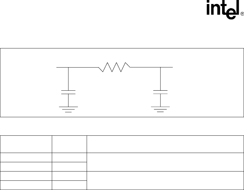
IXF1104 4-Port Gigabit Ethernet Media Access Controller
64 Datasheet
Document Number: 278757
Revision Number: 007
Revision Date: March 25, 2004
Figure 6. Analog Power Supply Filter Network
Table 21. Analog Power Balls
Signal Name Ball
Designator Comments
AVDD1P8_1 A5 A20 Need to provide a filter (see Figure 6).
R: AVDD1P8_1 and AVDD2P5_1 = 5.6 Ω resistor.
AVDD2P5_1 AD20
AVDD1P8_2 AB16 T23 Need to provide a filter (see Figure 6).
R: AVDD1P8_2 and AVDD2P5_2 = 1.0 Ω resistor.
AVDD2P5_2 U14 R18
0.1 µF
VDD
0.1 µF
Analog
Power Ba
ll
2.5 or 1.8 V R

IXF1104 Quad-Port 10/100/1000 Mbps Ethernet Media Access Controller
Datasheet 65
Document Number: 278757
Revision Number: 007
Revision Date: March 25, 2004
5.0 Functional Descriptions
5.1 Media Access Controller (MAC)
The IXF1104 main functional block consists of four independent 10/100/1000 Mbps Ethernet
MACs, which support interfaces for fiber and copper connectivity.
•Copper Mode:
— RGMII for 10/100/1000 Mbps full-duplex operation and 10/100 Mbps half-duplex
operation
— GMII for 1000 Mbps full-duplex operation
•Fiber Mode:
— Integrated SerDes/OMI interface for direct connection to optical modules
— 1000 Mbps full-duplex operation in fiber mode
The following features support copper and fiber modes:
•Programmable Options:
— Automatic padding of transmitted packets that are less than the minimum frame size
— Broadcast, multicast, and unicast address filtering on frames received
— Filter and drop packets with errors
— Pre-padded RX frames with two bytes (aligns the Ethernet payload on SPI3 and in
network processor memories)
— Remove CRC from RX frames
— Append CRC to transmitted frames
•Performance Monitoring and Diagnostics:
— Loopback modes
— Detection of runt and overly large packets
— Cyclic Redundancy Check (CRC) calculation and error detection
— RMON statistics for dropped packets, packets with errors, etc.
•Compliant with IEEE Spec 802.3x standard for flow control
— Receive and execute PAUSE Command Frames
•Support for non-standard packet sizes up to 10 KB including loss-less flow control
Note: The IXF1104 does not support 10/100 Mbps operation when configured in GMII mode
The MAC is fully integrated, designed for use with Ethernet 802.3 frame types, and compliant to
all of the IEEE 802.3 MAC requirements.
The MAC adds preamble and Start-of-Frame Delimiter (SFD) to all frames sent to it (transmit
path) and removes preamble and SFD on all frames received by it (receive path). A CRC check is
also applied to all transmit and receive packets. CRC is optionally appended to transmit packets.

IXF1104 Quad-Port 10/100/1000 Mbps Ethernet Media Access Controller
66 Datasheet
Document Number: 278757
Revision Number: 007
Revision Date: March 25, 2004
CRC is removed optionally from receive packets after validation, and is not forwarded to SPI3.
Packets with a bad CRC are marked, counted in the statistics block, and may be optionally
dropped. A bad packet may be signaled with RERR on the SPI3 interface if it is not dropped.
The MAC operates only in full-duplex mode at 1000 Mbps rates on both SerDes and GMII
interface connections. The MAC is capable of operation at 1000 Mbps, full-duplex in RGMII
mode, and at full-duplex and half-duplex operation for 10/100 Mbps links.
5.1.1 Features for Fiber and Copper Mode
Section 5.1.1.1 through Section 5.1.1.4 cover MAC functions that are independent of the line-side
interface.
5.1.1.1 Padding of Undersized Frames on Transmit
The padding feature allows Ethernet frames smaller than 64 bytes to be transferred from the SPI3
interface to the TX MAC and padded up to 64 bytes automatically by the MAC. This feature is
enabled by setting bit 7 of the “Diverse Config Write ($ Port_Index + 0x18)".
Note: When the user selects the padding function, the MAC core adds an automatically calculated CRC
to the end of the transmitted packet.
5.1.1.2 Automatic CRC Generation
Automatic CRC Generation is used in conjunction with the padding feature to generate and append
a correct CRC to any transmit frame. This feature is enabled by setting bit 6 of the “Diverse Config
Write ($ Port_Index + 0x18)".
5.1.1.3 Filtering of Receive Packets
This feature allows the MAC to filter receive packets under various conditions and drop the
packets through an interaction with the Receive FIFO control.
5.1.1.3.1 Filter on Unicast Packet Match
This feature is enabled when bit 0 of the “RX Packet Filter Control ($ Port_Index + 0x19)" = 1.
Any frame received in this mode that does not match the Station Address (MAC address) is marked
by the MAC to be dropped. The frame is dropped if the appropriate bit in the “RX FIFO Errored
Frame Drop Enable ($0x59F)" = 1. Otherwise, the frame is sent out the SPI3 interface and may
optionally be signaled with an RERR (see bit 0 in “SPI3 Receive Configuration ($0x701)” on
page 214).
When bit 0 of the “RX Packet Filter Control ($ Port_Index + 0x19)" = 0, all unicast frames are sent
out the SPI3 interface.
Note: The VLAN filter overrides the unicast filter. Therefore, a VLAN frame cannot be filtered based on
the unicast address.

IXF1104 Quad-Port 10/100/1000 Mbps Ethernet Media Access Controller
Datasheet 67
Document Number: 278757
Revision Number: 007
Revision Date: March 25, 2004
5.1.1.3.2 Filter on Multicast Packet Match
This feature is enabled when bit 1 of the “RX Packet Filter Control ($ Port_Index + 0x19)" = 1.
Any frame received in this mode that does not match the Port Multicast Address (reserved
multicast address recognized by MAC) is marked by the MAC to be dropped. The frame is dropped
if the appropriate bit in the “RX FIFO Errored Frame Drop Enable ($0x59F)" = 1. Otherwise, the
frame is sent out the SPI3 interface and may optionally be signaled with an RERR (see bit 0 in
“SPI3 Receive Configuration ($0x701)” on page 214).
When bit 1 of the “RX Packet Filter Control ($ Port_Index + 0x19)" = 0, all multicast frames are
sent out the SPI3 interface.
5.1.1.3.3 Filter Broadcast Packets
This feature is enabled when bit 2 of the “RX Packet Filter Control ($ Port_Index + 0x19)" = 1.
Any broadcast frame received in this mode is marked by the MAC to be dropped. The frame is
dropped if the appropriate bit in the “RX FIFO Errored Frame Drop Enable ($0x59F)" = 1.
Otherwise, the frame is sent out the SPI3 interface and may optionally be signaled with an RERR
(see bit 0 in “SPI3 Receive Configuration ($0x701)” on page 214).
When bit 2 of the “RX Packet Filter Control ($ Port_Index + 0x19)" = 0, all broadcast frames are
sent out the SPI3 interface.
5.1.1.3.4 Filter VLAN Packets
This feature is enabled when bit 3 of the “RX Packet Filter Control ($ Port_Index + 0x19)" = 1.
VLAN frames received in this mode are marked by the MAC to be dropped. The frame is dropped
if the appropriate bit in the “RX FIFO Errored Frame Drop Enable ($0x59F)" = 1. Otherwise, the
VLAN frame is sent out the SPI3 interface and may optionally be signaled with an RERR (see bit 0
in “SPI3 Receive Configuration ($0x701)” on page 214).
When bit 3 of the “RX Packet Filter Control ($ Port_Index + 0x19)" = 0, all VLAN frames are sent
out the SPI3 interface.
5.1.1.3.5 Filter Pause Packets
This feature is enabled when bit 4 of the “RX Packet Filter Control ($ Port_Index + 0x19)" = 0.
Pause frames received in this mode are marked by the MAC to be dropped. The frame is dropped if
the appropriate bit in the “RX FIFO Errored Frame Drop Enable ($0x59F)" = 1. Otherwise, the
pause frame is sent out the SPI3 interface and may optionally be signaled with an RERR (see bit 0
in “SPI3 Receive Configuration ($0x701)” on page 214).
When bit 4 of the “RX Packet Filter Control ($ Port_Index + 0x19)" = 1, all pause frames are sent
out the SPI3 interface.
Note: Pause packets are not filtered if flow control is disabled in the “FC Enable ($ Port_Index + 0x12)”.
5.1.1.3.6 Filter CRC Error Packets
This feature is enabled when bit 5 of the “RX Packet Filter Control ($ Port_Index + 0x19)” = 0.
Frames received with an errored CRC are marked as bad frames and may optionally be dropped in
the RX FIFO. Otherwise, the frames are sent to the SPI3 interface and may be optionally signaled
with an RERR (see Table 22 “CRC Errored Packets Drop Enable Behavior” on page 68).

IXF1104 Quad-Port 10/100/1000 Mbps Ethernet Media Access Controller
68 Datasheet
Document Number: 278757
Revision Number: 007
Revision Date: March 25, 2004
When the CRC Error Pass Filter bit = 0 (“RX Packet Filter Control ($ Port_Index + 0x19)”), it
takes precedence over the other filter bits. Any packet (Pause, Unicast, Multicast or Broadcast
packet) with a CRC error will be marked as a bad frame when the CRC Error Pass Filter bit = 0.
5.1.1.4 CRC Error Detection
Frames received by the MAC are checked for a correct CRC. When an incorrect CRC is detected
on a received frame, the RX FCSError RMON statistic counter is incremented for each CRC
errored frame. Received frames with CRC errors may optionally be dropped in the RX FIFO (refer
to Section 5.1.1.3.6, “Filter CRC Error Packets” on page 67). Otherwise, the frames are sent to the
SPI3 interface and may be dropped by the switch or system controller.
Frames transmitted by the MAC are also checked for correct CRC. When an incorrect CRC is
detected on a transmitted frame, the TX CRCError RMON statistic counter is incremented for each
incorrect frame.
5.1.2 Flow Control
Flow Control is an IEEE 802.3x-defined mechanism for one network node to request that its link
partner take a temporary “Pause” in packet transmission. This allows the requesting network node
to prevent FIFO overruns and dropped packets, by managing incoming traffic to fit its available
memory. The temporary pause allows the device to process packets already received or in transit,
thus freeing up the FIFO space allocated to those packets.
Table 22. CRC Errored Packets Drop Enable Behavior
CRC Error
Pass1
RX FIFO Errored-
Frame Drop
Enable2
RERR
Enable3Actions
1xx
When CRC Errored PASS = 1, CRC errored packets
are not filtered and are passed to the SPI3 interface.
They are not marked as bad, cannot be dropped, and
cannot be signaled with RERR.
001
Packets are marked as bad but not dropped in the
RX FIFO. These packets are sent to the SPI3
interface, and are signaled with an RERR to the
switch or Network Processor.
000
Packets are marked as bad but not dropped in the
RX FIFO. These packets are sent to the SPI3
interface, and are not signaled with an RERR.
01x
CRC errored packets are marked as bad, dropped in
the RX FIFO, and never appear at the SPI3 interface.
NOTE: Packet sizes above the RX FIFO Transfer
Threshold (see Table 128 through Table 131)
cannot be dropped in the RX FIFO and are
passed to the SPI3 interface. These packets
can optionally be signaled with RERR on the
SPI3 interface if the RERR Enable bit = 1.
1. See Table 91 “RX Packet Filter Control ($ Port_Index + 0x19)” on page 171.
2. See Table 123 “RX FIFO Errored Frame Drop Enable ($0x59F)” on page 195.
3. See Table 147 “SPI3 Receive Configuration ($0x701)” on page 214.
NOTE: x = “DON’T CARE”

IXF1104 Quad-Port 10/100/1000 Mbps Ethernet Media Access Controller
Datasheet 69
Document Number: 278757
Revision Number: 007
Revision Date: March 25, 2004
The IXF1104 MAC implements the IEEE 802.3x standard RX FIFO threshold-based Flow Control
in copper and fiber modes. When appropriately programmed, the MAC can both generate and
respond to IEEE standard pause frames in full-duplex operation. The IXF1104 also supports
externally triggered flow control through the Transmit Pause Control interface.
In half-duplex operation, the MAC generates collisions instead of sending pause frames to manage
the incoming traffic from the link partner
5.1.2.1 802.3x Flow Control (Full-Duplex Operation)
The IEEE 802.3x standard identifies four options related to system flow control:
•No Pause
•Symmetric Pause (both directions)
•Asymmetric Pause (Receive direction only)
•Asymmetric Pause (Transmit direction only)
The IXF1104 supports all four options on a per-port basis. Bits 2:0 of the “FC Enable ($ Port_Index
+ 0x12)” on page 167 provide programmable control for enabling or disabling flow control in each
direction independently.
The IEEE 802.3x flow control mechanism is accomplished within the MAC sublayer, and is based
on RX FIFO thresholds called watermarks. The RX FIFO level rises and falls as packets are
received and processed. When the RX FIFO reaches a watermark (either exceeding a High or
dropping below a Low after exceeding a High), the IXF1104 control sublayer signals an internal
state machine to transmit a PAUSE frame. The FIFOs automatically generate PAUSE frames (also
called control frames) to initiate the following:
•Halt the link partner when the High watermark is reached.
•Restart the link partner when the data stored in the FIFO falls below the Low watermark.
Figure 7 illustrates the IEEE 802.3 FIFO flow control functions.
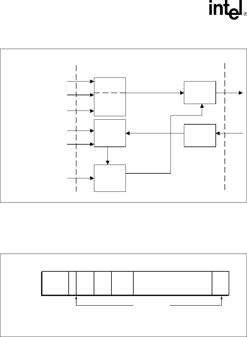
IXF1104 Quad-Port 10/100/1000 Mbps Ethernet Media Access Controller
70 Datasheet
Document Number: 278757
Revision Number: 007
Revision Date: March 25, 2004
5.1.2.1.1 Pause Frame Format
PAUSE frames are MAC control frames that are padded to the minimum size (64 bytes). Figure 8
and Figure 9 illustrate the frame format and contents.
Figure 7. Packet Buffering FIFO
MDI
High Watermark
Data Flow
M
AC Transfer Threshold
Low Watermark
High Watermark Data Flow
Low Watermark
RX FIFO High
TXPAUSEFR (External
Strobe) 802.3x Pause Frame Generation
TX FIFO TX Side
MAC
RX FIFO
802.3 Flow
Control
RX Side
MAC
SPI3 Interface
B3231-01
Figure 8. Ethernet Frame Format
B2277-01
DA SA Data FCS
Type/
Length
S
F
D
Preamble
61 46 6 2 46-1500
Ethernet Frame
Number of bytes
Note: 64 Byte Minimum / 1518 bytes Maximum
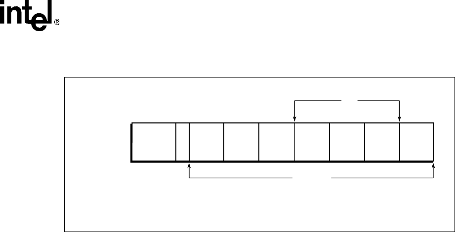
IXF1104 Quad-Port 10/100/1000 Mbps Ethernet Media Access Controller
Datasheet 71
Document Number: 278757
Revision Number: 007
Revision Date: March 25, 2004
An IEEE 802.3 MAC PAUSE frame is identified by detecting all of the following:
•OpCode of 00-01
•Length/Type field of 88-08
•DA matching the unique multicast address (01-80-C2-00-00-01)
XOFF. A PAUSE frame informs the link partner to halt transmission for a specified length of time.
The PauseLength octets specify the duration of the no-transmit period. If this time is greater than
zero, the link partner must stop sending any further packets until this time has elapsed. This is
referred to as XOFF.
XON. The MAC continues to transmit PAUSE frames with the specified Pause Length as long as
the FIFO level exceeds the threshold. If the FIFO level falls below the threshold before the Pause
Length time expires, the MAC sends another PAUSE frame with the Pause Length time specified
as zero. This is referred to as XON and informs the link partner to resume normal transmission of
packets.
5.1.2.1.2 Pause Settings
The MAC must send PAUSE frames repeatedly to maintain the link partner in a Pause state. The
following two inter-related variables control this process:
•Pause Length is the amount of time, measured in multiples of 512 bit times, that the MAC
requests the link partner to halt transmission for.
•Pause Threshold is the amount of time, measured in multiples of 512 bit times, prior to the
expiration of the Pause Length that the MAC transmits another Pause frame to maintain the
link partner in the pause state.
The transmitted Pause Length in the IXF1104 is set by the “FC TX Timer Value ($ Port_Index +
0x07)” on page 163.
The IXF1104 PAUSE frame transmission interval is set by the “Pause Threshold ($ Port_Index +
0x0E)” on page 165.
Figure 9. PAUSE Frame Format
B3218-01
DA* or
01-80-
C2-00-
00-01
SA 88-08 FCS
S
F
D
Preamble
61 4662
Pause
Opcode
(00-01)
Pause
Length
22
46
Pad
(with 0s)
42
64 Bytes
Number of bytes
Note: In the Intel® IXF1104 architecture, the TX block of the MAC sets this as the pause multicast address.
The RX interface of the MAC will process this as the pause multicast or the MAC address.

IXF1104 Quad-Port 10/100/1000 Mbps Ethernet Media Access Controller
72 Datasheet
Document Number: 278757
Revision Number: 007
Revision Date: March 25, 2004
5.1.2.1.3 Response to Received PAUSE Command Frames
When Flow Control is enabled in the receive direction (bit 0 in the “FC Enable ($ Port_Index +
0x12)"), the IXF1104 responds to PAUSE Command frames received from the link partner as
follows:
1. The IXF1104 checks the entire frame to verify that it is a valid PAUSE control frame
addressed to the Multicast Address 01-80-C2-00-00-01 (as specified in IEEE 802.3, Annex
31B) or has a Destinations Address matching the address programmed in the “Station Address
($ Port_Index +0x00 – +0x01)".
2. If the PAUSE frame is valid, the transmit side of the IXF1104 pauses for the required number
of PAUSE Quanta, as specified in IEEE 802.3, Clause 31.
3. PAUSE does not begin until completion of the frame currently being transmitted.
The IXF1104 response to valid received PAUSE frames is independent of the PAUSE frame filter
settings. Refer to Section 5.1.1.3.5, “Filter Pause Packets” on page 67 for additional details.
Note: Pause packets are not filtered if flow control is disabled in bit 0 of the “FC Enable ($ Port_Index +
0x12)”.
5.1.2.1.4 Half-Duplex Operation
Transmit flow control is implemented only in half-duplex operation. Upon entering the flow
control state, the MAC generates a collision for all subsequent receive packets until exiting the
flow control state. Any receive packet in progress when the MAC enters the flow control state will
not be collided with but could be lost due if there is insufficient FIFO depth to complete packet
reception. Bit 2 of the “FC Enable ($ Port_Index + 0x12)" enables the transmit flow control
function.
5.1.2.1.5 Transmit Pause Control Interface
The Transmit Pause Control interface allows an external device to trigger the generation of pause
frames. The Transmit Pause Control interface is completely asynchronous. It consists of three
address signals (TXPAUSEADD[2:0]) and a strobe signal (TXPAUSEFR). The required address
for this interface operation is placed on the TXPAUSEADD[2:0] signals and the TXPAUSEFR is
pulsed High and returned Low. Refer to Figure 10 “Transmit Pause Control Interface” on page 73
and Table 55 “Transmit Pause Control Interface Timing Parameters” on page 150. Table 23 shows
the valid decodes for the TXPAUSEADD[2:0] signals. Figure 10 illustrates the transmit pause
control interface.
Note: Flow control must be enabled in the “FC Enable ($ Port_Index + 0x12)” for Transmit Pause
Control interface operation.
Note: There are two additional decodes provided that allow the user to generate either an XOFF frame or
XON frame from all ports simultaneously.
The default pause quanta for each port is held by the “FC TX Timer Value ($ Port_Index + 0x07)").
The default value of this register is 0x05E after reset is applied.
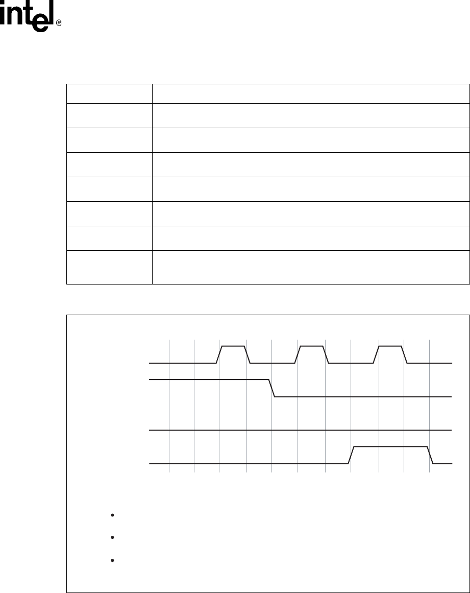
IXF1104 Quad-Port 10/100/1000 Mbps Ethernet Media Access Controller
Datasheet 73
Document Number: 278757
Revision Number: 007
Revision Date: March 25, 2004
Table 23. Valid Decodes for TXPAUSEADD[2:0]
TXPAUSEADD_2:0 Operation of TX Pause Control Interface
0x0 Transmits a PAUSE frame on every port with a pause_time = ZERO (XON)
(Cancels all previous pause commands).
0x1 Transmits a PAUSE frame on port 0 with pause_time equal to the value programmed
in the port 0 “FC TX Timer Value ($ Port_Index + 0x07)" (XOFF).
0x2 Transmits a PAUSE frame on port 1 with pause_time equal to the value programmed
in the port 1 “FC TX Timer Value ($ Port_Index + 0x07)" (XOFF).
0x3 Transmits a PAUSE frame on port 2 with pause_time equal to the value programmed
in the port 2 “FC TX Timer Value ($ Port_Index + 0x07)" (XOFF).
0x4 Transmits a PAUSE frame on port 3 with pause_time equal to the value programmed
in the port 3 “FC TX Timer Value ($ Port_Index + 0x07)" (XOFF).
0x5 to 0x6 Reserved. Do not use these addresses. The TX Pause Control interface will not
operate under these conditions.
0x7 Transmits a PAUSE frame on every port with pause_time equal to the value
programmed in the “FC TX Timer Value ($ Port_Index + 0x07)" for each port
(XOFF).
Figure 10. Transmit Pause Control Interface
B3234-01
TXPAUSEFR
TXPAUSEADD0
TXPAUSEADD1
TXPAUSEADD2
This example shows the following conditions:
Strobe 1:
Port 0: Transmit Pause Packet (XOFF)
Strobe 2:
All Ports: Transmit Pause Packet with pause_time = 0 (XON)
Strobe 3:
Port 3: Transmit Pause Packet (XOFF)

IXF1104 Quad-Port 10/100/1000 Mbps Ethernet Media Access Controller
74 Datasheet
Document Number: 278757
Revision Number: 007
Revision Date: March 25, 2004
5.1.3 Mixed-Mode Operation
The Intel® IXF1104 gives the user the option of configuring each port for 10/100 Mbps half-duplex
copper, 10/100/1000 Mbps full-duplex copper, or 1000 Mbps full-duplex fiber operation. This
gives the Intel® IXF1104 the ability to support both copper and fiber operation line-side interfaces
operating at the same time within a single device. (Refer to Figure 16 “Line Side Interface
Multiplexed Balls” on page 57.)
The Intel® IXF1104 provides complete flexibility in line-side connectivity by offering RGMII,
integrated SerDes, and GMII.
5.1.3.1 Configuration of the IXF1104
The memory maps (Table 59 “MAC Control Registers ($ Port Index + Offset)” on page 155
through Table 69 “Optical Module Registers ($ 0x799 - 0x79F)” on page 161) are logically split
into the following two distinct regions:
•Per-Port Registers
•Global Registers
To achieve a desired configuration for a given port, the relevant per-port registers must be
configured correctly by the user. The Table 59 through Table 69 also contain registers that affect
the operation of all ports, such as the SPI3 interface configuration.
See Section 8.0, “Register Set” on page 154 for a complete description of IXF1104 configuration
and status registers. The Register Maps (Table 59 through Table 69) present a summary of
important configuration registers.
Note: The initialization sequence provided in Section 6.1, “Change Port Mode Initialization Sequence”
on page 129 must be followed for proper configuration of the IXF1104.
5.1.3.2 Key Configuration Registers
The following key registers select the operational mode of a given port:

IXF1104 Quad-Port 10/100/1000 Mbps Ethernet Media Access Controller
Datasheet 75
Document Number: 278757
Revision Number: 007
Revision Date: March 25, 2004
5.1.4 Fiber Mode
When the IXF1104 is configured for fiber mode, the TX Data path from the MAC is an internal
10-bit interface as described in the IEEE 802.3z specification. It is connected directly to an internal
SerDes block for serialization/deserialization and transmission/reception on the fiber medium to
and from the link partner.
The MAC contains all of the PCS (8B/10B encoding and 10B/8B decoding) required to encode and
decode the data. The MAC also supports auto-negotiation per the IEEE 802.3z specification via
access to the “TX Config Word ($ Port_Index + 0x17)", “RX Config Word ($ Port_Index + 0x16)",
and “Diverse Config Write ($ Port_Index + 0x18)".
Table 24. Operational Mode Configuration Registers
Register Name Register
Address Description
“Desired Duplex
($ Port_Index +
0x02)"
0x002 – Port 0
0x082 – Port 1
0x102 – Port 2
0x182 – Port 3
The “Desired Duplex ($ Port_Index + 0x02)” on page 162 defines
whether a port is to be configured for full-duplex or half-duplex
operation.
NOTE: Half-duplex operation is only valid for 10/100 speeds where the
RGMII line interface has been selected.
“MAC IF Mode
and RGMII
Speed ($
Port_Index +
0x10)"
0x010 – Port 0
0x090 – Port 1
0x110 – Port 2
0x190 – Port 3
The “MAC IF Mode and RGMII Speed ($ Port_Index + 0x10)” on
page 166 determines the MAC operational frequency and mode for a
given port.
NOTE: Set the “Clock and Interface Mode Change Enable Ports 0 - 3
($0x794)” on page 220 to 0x0 prior to any change in the
register value. This ensures that a change in the MAC clock
frequency is controlled correctly. If the “Clock and Interface
Mode Change Enable Ports 0 - 3 ($0x794)" is not used
correctly, the IXF1104 may not be configured to the proper
mode.
“Port Enable
($0x500)"
0x500
Bit 0 – Port 0
Bit 1 – Port 1
Bit 2 – Port 2
Bit 3 – Port 3
Each “Port Enable ($0x500)" bit relates to a port. Set the appropriate bit
to 0x1 to enable a port. This should be the last step in the configuration
process for a port.
“Interface Mode
($0x501)"
0x501
Bit 0 – Port 0
Bit 1 – Port 1
Bit 2 – Port 2
Bit 3 – Port 3
The “Interface Mode ($0x501)" selects whether a port operates with a
copper (RGMII or GMII) line-side interface an integrated SerDes fiber
line-side interface.
For copper operation for a given port, set the relevant bit to 0x1.
For fiber operation for a given port, set the relevant bit to 0x0.
NOTE: All ports are configured for fiber operation in the IXF1104
default mode of operation.
“Clock and
Interface Mode
Change Enable
Ports 0 - 3
($0x794)"
0x794
Bit 0 – Port 0
Bit 1 – Port 1
Bit 2 – Port 2
Bit 3 – Port 3
The “Clock and Interface Mode Change Enable Ports 0 - 3 ($0x794)"
indicates to an internal clock generator when to sample the new value
of the “MAC IF Mode and RGMII Speed ($ Port_Index + 0x10)" and the
“Interface Mode ($0x501)" (copper/fiber).
When any of these two configuration values are changed for a port, the
corresponding bits must be kept in this register under reset by writing
0x0 to the relevant bit.
NOTE: The initialization sequence provided in Section 6.1, “Change Port Mode Initialization
Sequence” on page 129 must be followed for proper configuration of the IXF1104.

IXF1104 Quad-Port 10/100/1000 Mbps Ethernet Media Access Controller
76 Datasheet
Document Number: 278757
Revision Number: 007
Revision Date: March 25, 2004
When configured for fiber mode, the full set of Optical Module interface control and status signals
is presented through re-use of GMII signals on a per-port basis (see Table 4.5 “Multiplexed Ball
Connections” on page 57). Fiber mode supports only full-duplex Gigabit operation.
5.1.4.1 Fiber Auto-Negotiation
Auto-negotiation is performed by using the “TX Config Word ($ Port_Index + 0x17)", “RX Config
Word ($ Port_Index + 0x16)", and “Diverse Config Write ($ Port_Index + 0x18)". When
autoneg_enable (“Diverse Config Write ($ Port_Index + 0x18)") is set, the IXF1104 performs
hardware-defined auto-negotiation with the “TX Config Word ($ Port_Index + 0x17)" used as an
“Auto-Negotiation Advertisement ($ Port Index + 0x64)" and the “RX Config Word ($ Port_Index
+ 0x16)" used as an “Auto-Negotiation Link Partner Base Page Ability ($ Port Index + 0x65)".
Note: While the MAC supports auto-negotiation functions, the IXF1104 does not automatically configure
the MAC or other device blocks to be consistent with the auto-negotiation results. This
configuration is done by the user and system software.
5.1.4.2 Determining If Link Is Established in Auto-Negotiation Mode
A valid link is established when the AN_complete bit is set and the RX_Sync bit reports that
synchronization has occurred. Both register bits are located in the “RX Config Word ($ Port_Index
+ 0x16)".
If the link goes down after auto-negotiation is completed, RX_Sync indicates that a loss of
synchronization occurred. The IXF1104 restarts auto-negotiation and attempts to reestablish a link.
Once a link is reestablished, the AN_complete bit is set and the RX_Sync bit shows that
synchronization has occurred.
To manually restart auto-negotiation, bit 5 of the “Diverse Config Write ($ Port_Index + 0x18)”
(AN_enable) must be de-asserted, then re-asserted.
5.1.4.3 Fiber Forced Mode
The MAC fiber operation can be forced to operate at 1000 Mbps full-duplex without completion of
the auto-negotiation function. In this mode, the MAC RX path must achieve synchronization with
the link partner. Once achieved, the MAC TX path is enabled to allow data transmission. This
forced mode is limited to operation with a link partner that operates with a full-duplex link at
1000 Mbps.
5.1.4.4 Determination of Link Establishment in Forced Mode
When the IXF1104 is in forced mode operation, the “RX Config Word ($ Port_Index + 0x16)” bit
20 RX Sync indicates when synchronization occurs and a valid link establishes.
Note: The RX Sync bit indicates a loss of synchronization when the link is down.
5.1.5 Copper Mode
In copper mode, the IXF1104 transmits data on the egress path of the RGMII or GMII interface,
depending on the port configuration defined by the user. The copper MAC receives data on the
ingress path of the RGMII or GMII interface, depending on the port configuration defined by the

IXF1104 Quad-Port 10/100/1000 Mbps Ethernet Media Access Controller
Datasheet 77
Document Number: 278757
Revision Number: 007
Revision Date: March 25, 2004
user. The RGMII interface supports operation at 10/100/1000 Mbps when a full-duplex link is
established, and supports 10/100 Mbps when a half-duplex link is established. The GMII interface
only supports a 1000 Mbps full-duplex link.
5.1.5.1 Speed
The copper MAC supports 10 Mbps, 100 Mbps, and 1000 Mbps. All required speed adjustments,
clocks, etc., are supplied by the MAC. The operating speed of the MAC is programmable through
the “MAC IF Mode and RGMII Speed ($ Port_Index + 0x10)" (MAC_IF_Mode). The IXF1104
speed setting must be programmed by the system software to match the speed of the attached PHY
for proper IXF1104 operation.
Note: When the IXF1104 is configured to use the GMII interface, the only mode of operation that is
supported is 1000 Mbps full-duplex.
If 10/100 Mbps operation is required in either full-duplex or half-duplex, the IXF1104 must be
configured to use the RGMII interface.
5.1.5.2 Duplex
The MAC supports full-duplex or half-duplex depending on the line-side interface that is
configured by the “MAC IF Mode and RGMII Speed ($ Port_Index + 0x10)" (MAC_IF_Mode).
The duplex of the MAC is set in the “Desired Duplex ($ Port_Index + 0x02)” on page 162. The
IXF1104 duplex setting must be programmed by the system software to match the attached PHY
duplex for proper IXF1104 operation.
5.1.5.3 Copper Auto-Negotiation
In the copper MAC, auto-negotiation and all other controls of the PHY devices are achieved
through the MDIO interface, and are independent of the MAC controller. See Section 5.5, “MDIO
Control and Interface” on page 98 for further operation details.
Note: In copper mode, auto-negotiation is accomplished by the attached PHY, not the IXF1104. Thus, the
IXF1104 does not automatically configure the MAC or other blocks in the device to be consistent
with attached PHY auto-negotiation results. This must be accomplished by the user and system
software.
5.1.6 Jumbo Packet Support
The IXF1104 supports jumbo frames. The jumbo frame length is dependent on the application and
the IXF1104 design is optimized for a 9.6 KB jumbo frame length. Larger lengths can be
programmed, but limited system performance may lead to data loss during certain flow-control
conditions
The value programmed into the“Max Frame Size (Addr: Port_Index + 0x0F)" determines the
maximum length frame size the MAC can receive or transmit without activating any error counters,
and without truncation.
The“Max Frame Size (Addr: Port_Index + 0x0F)" bits 13:0 set the frame length. The default value
programmed into this register is 0x05EE (1518). The value is internally adjusted by +4 if the frame
has a VLAN tag. The overall programmable maximum is 0x3FFF or 16383 bytes.

IXF1104 Quad-Port 10/100/1000 Mbps Ethernet Media Access Controller
78 Datasheet
Document Number: 278757
Revision Number: 007
Revision Date: March 25, 2004
The register should be programmed to 0x2667 for the 9.6 KB length jumbo frame, optimized for
the IXF1104. The RMON counters are also implemented for jumbo frame support as follows:
5.1.6.1 Rx Statistics
•RxOctetsTotalOK (Addr: Port_Index + 0x20)
•RxPkts1519toMaxOctets (Addr: Port_Index + 0x2B)
•RxFCSErrors (Addr: Port_Index + 0x2C)
•RxDatatError (Addr: Port_Index = 0x02E)
•RxAlignErrors (Addr: Port_Index + 0x2F)
•RxLongErrors (Addr: Port_Index + 0x30)
•RxJabberErrors (Addr: Port_Index + 0x31)
•RxVeryLongErrors (Addr: Port_Index + 0x34)
5.1.6.2 TX Statistics
•OctetsTransmittedOK (Addr: Port_Index + 0x40)
•TxPkts1519toMaxOctets (Addr: Port_Index + 0x4B)
•TxExcessiveLengthDrop (Addr: Port_Index + 0x53)
•TxCRCError (Addr: Port_Index + 0x56)
The IXF1104 checks the CRC for all legal-length jumbo frames (frames between 1519 and the
Max Frame Size). On transmission, the MAC can be programmed to append the CRC to the frame
or check the CRC and increment the appropriate counter. On reception, the MAC transmits these
frames across the SPI3 interface (jumbo frames above the setting in the “RX FIFO Transfer
Threshold Port 0 ($0x5B8)” with a bad CRC cannot be dropped and are sent across the SPI3
interface). If the receive frame has a bad CRC, the appropriate counter is incremented and the
RxERR flag is asserted on the SPI3 receive interface.
Jumbo frames also impact flow control. The maximum frame size needs to be taken into account
when determining the FIFO watermarks. The current transmission must be completed before a
Pause frame is transmitted (needed when the receiver FIFO High watermark is exceeded). If the
current transmission is a jumbo frame, the delay may be significant and increase data loss due to
insufficient available FIFO space.
5.1.6.3 Loss-less Flow Control
The IXF1104 supports loss-less flow control when the size of a Jumbo packet is restricted to
9.6 k bytes. If this condition is met, the IXF1104 has sufficient memory resources allocated to each
MAC port to ensure that, if both the IXF1104 and link partner are required to send Pause packets
simultaneously during jumbo packet transfers across a medium of five kilometers of fiber, no
packet data should be lost due to FIFO overflows.

IXF1104 Quad-Port 10/100/1000 Mbps Ethernet Media Access Controller
Datasheet 79
Document Number: 278757
Revision Number: 007
Revision Date: March 25, 2004
5.1.7 Packet Buffer Dimensions
5.1.7.1 TX and RX FIFO Operation
5.1.7.1.1 TX FIFO
The IXF1104 TX FIFOs are implemented with 10 KB for each channel. This provides enough
space for at least one maximum size (10 KB) packet per-port storage and ensures that no under-run
conditions occur, assuming that the sending device can supply data at the required data rate.
A transfer to MAC Threshold parameter, which is user-programmable, determines when the FIFO
signals to the MAC that it has data to send. This is configured for specific block sizes, and the user
must ensure that an under-run does not occur. Also, the threshold can be set above the maximum
size of a normal Ethernet packet. This causes the FIFO to send only data to the MAC when this
threshold is exceeded or when the End-of-Packet marker is received. This second condition
eliminates the possibility of under-run, except when the controlling switch device fails. It can,
however, cause idle times on the media.
5.1.7.1.2 RX FIFO
The IXF1104 RX FIFOs are provisioned so that each port has its own 32 KB of memory space.
This is enough memory to ensure that there is never an over-run on any channel while transferring
normal Ethernet frame size data.
The FIFOs automatically generate Pause control frames to halt the link partner when the High
watermark is reached and to restart the link partner when the data stored in the FIFO falls below the
low-watermark. The RX and TX FIFOs have been sized to support lossless flow control with
9.6 KB packets. The RX FIFO has a programmable transfer threshold that sets the threshold at
which packets become “cut through” and starts transitioning to the SPI3 interface before the EOP
is received. Packets sizes below this threshold are treated as “store and forward.” Once a packet
size exceeds the RX FIFO transfer threshold, it can no longer be dropped by the RX FIFO even if it
is marked to be dropped by the MAC.
5.1.8 RMON Statistics Support
The IXF1104 supplies RMON statistics through the CPU interface. These statistics are available in
the form of counter values that can be accessed at specific addresses in the register maps (Table 59
through Table 69). Once read, these counters automatically reset and begin counting from zero. A
separate set of RMON statistics is available for each MAC device in the IXF1104.
Implementation of the RMON Statistics block is similar to the functionality provided by existing
Intel switch and router products. This implementation allows the IXF1104 to provide all of the
RMON Statistics group as defined by RFC2819. The IXF1104 supports the RMON RFC2819
Group 1 statistics counters. Table 25 notes the differences and additional statistics registers
supported by the IXF1104 that are outside the scope of the RMON RFC2819 document.

IXF1104 Quad-Port 10/100/1000 Mbps Ethernet Media Access Controller
80 Datasheet
Document Number: 278757
Revision Number: 007
Revision Date: March 25, 2004
Table 25. RMON Additional Statistics (Sheet 1 of 2)
RMON Ethernet Statistics
Group 1 Statistics Type IXF1104-Equivalent
Statistics Type Definition of RMON
Versus IXF1104
Documentation
etherStatsindex Integer 32 NA NA NA
etherStatsDataSource Object
identifier NA NA NA
etherStatsDropEvents Counter
32
RX Number of Frames
Removed/
TX Number of Frames
Removed
Counter 32 See table note 1
etherStatsOctets Counter
32
RxOctetsTotalOK
RxOctetsBad
OctetsTransmittedOK
OctetsTransmittedBad
Counter 32
The IXF1104 has two
counters for receive
and transmit that use
different naming
conventions for the
total Octets and
Octets Bad. These
counters must be
combined to meet
the RMON definition
for this statistic.
etherStatsPkts Counter32
RxUCPkts/TxUCPkts
RxBCPkts/TxBCPkts
RxMCPkts/TxMCPkts
Counter 32
The IXF1104 has
three counters for the
etherStatsPkts that
must be combined to
give the total packets
as defined by the
RMON specification.
etherStatsBroadcastPkts Counter32 RxBCPkts/TxBCPkts Counter 32 Same as RMON
specification
etherStatsMulticastPkts Counter32 RxMCPkts/TxMCPkts Counter 32 See table note 2
etherStatsCRCAlignErrors Counter32
RxAlignErrors
RxFCSErrors
TxCRCError
Counter 32
The IXF1104 has two
counters for the
alignment and CRC
errors for the RX side
only.
The IXF1104 has a
CRC Error counter
for the TX side.
etherStatsUndersizedPkts Counter32
RxRuntErrors
RxShortErrors
Rx Statistics ONLY
Counter 32
The IXF1104 has two
counters, one for
Runt errors and one
for ShortErrors.
etherStatsOversizePkts Counter32 RxLongErrors
TxExcessiveLength Drop Counter 32 Same as RMON
specification
NOTE: The RMON specification requires that this is, “The total number of events where packets were dropped
by the probe due to a lack of resources. This number is not necessarily the number of packets dropped;
it is the number of times this condition is detected." The “RX FIFO Overflow Frame Drop Counter Ports 0
- 3 ($0x594 – 0x597)" and “TX FIFO Overflow Frame Drop Counter Ports 0 - 3 ($0x621 – 0x624)" in the
IXF1104 support this and increment when either an RX FIFO or TX FIFO overflows. If any IXF1104
programmable packet filtering is enabled, the “RX FIFO Errored Frame Drop Counter Ports 0 - 3 ($0x5A2
- 0x5A5)" and “TX FIFO Errored Frame Drop Counter Ports 0 - 3 ($0x625 – 0x629)" increment with every
frame removed in addition to the existing frames counted due to FIFO overflow.

IXF1104 Quad-Port 10/100/1000 Mbps Ethernet Media Access Controller
Datasheet 81
Document Number: 278757
Revision Number: 007
Revision Date: March 25, 2004
5.1.8.1 Conventions
The following conventions are used throughout the RMON Management Information Base (MIB)
and its companion documents.
•Good Packets: Error-free packets that have a valid frame length. For example, on Ethernet,
good packets are error-free packets that are between 64 and 1518 octets long. They follow the
form defined in IEEE 802.3, Section 3.2.
•Bad Packets: Bad packets are packets that have proper framing and recognized as packets, but
contain errors within the packet or have an invalid length. For example, on Ethernet, bad
packets have a valid preamble and SFD, but have a bad CRC, or are either shorter than 64
octets or longer than 1518 octets.
etherStatsFragments Counter32 RuntErrors Counter 32 Same as RMON
specification
etherStatsJabbers Counter32 JabberErrors Counter 32 Same as RMON
specification
etherStatsCollisions Counter32
TxSingleCollision
TxMultipleCollision
TxLateCollision
TxTotalCollision
Counter 32
The TxTotalCollision
count value is
equivalent to the
RMON specification
minus the
TxLateCollision
etherStatsPkts64Octets Counter32 RxPkts64Octets/
TxPkts64Octets Counter 32 Same as RMON
specification
etherStatsPkts65to127Octets Counter32 RxPkts65to127Octets/
TxPkts65to127Octets Counter 32 Same a RMON
specification
etherStatsPkts128to255Octets Counter32 RxPkts128to255Octets/
TxPkts128to255Octets Counter32 Same a RMON
specification
etherStatsPkts256to511Octets Counter32 RxPkts256to511Octets/
TxPkts256to511Octets Counter32 Same a RMON
specification
etherStatsPkts512to1023Octets Counter32 RxPkts512to1023Octets/
TxPkts512to1023Octets Counter32 Same a RMON
specification
etherStatsPkts1023to1518Octets Counter32 RxPkts1023to1518Octets/
TxPkts1023to1518Octets Counter32 Same as RMON
specification
etherStatOwner Owner
String NA NA NA
etherStatsStatus Entry
Status NA NA NA
Table 25. RMON Additional Statistics (Sheet 2 of 2)
RMON Ethernet Statistics
Group 1 Statistics Type IXF1104-Equivalent
Statistics Type Definition of RMON
Versus IXF1104
Documentation
NOTE: The RMON specification requires that this is, “The total number of events where packets were dropped
by the probe due to a lack of resources. This number is not necessarily the number of packets dropped;
it is the number of times this condition is detected." The “RX FIFO Overflow Frame Drop Counter Ports 0
- 3 ($0x594 – 0x597)" and “TX FIFO Overflow Frame Drop Counter Ports 0 - 3 ($0x621 – 0x624)" in the
IXF1104 support this and increment when either an RX FIFO or TX FIFO overflows. If any IXF1104
programmable packet filtering is enabled, the “RX FIFO Errored Frame Drop Counter Ports 0 - 3 ($0x5A2
- 0x5A5)" and “TX FIFO Errored Frame Drop Counter Ports 0 - 3 ($0x625 – 0x629)" increment with every
frame removed in addition to the existing frames counted due to FIFO overflow.

IXF1104 Quad-Port 10/100/1000 Mbps Ethernet Media Access Controller
82 Datasheet
Document Number: 278757
Revision Number: 007
Revision Date: March 25, 2004
5.1.8.2 IXF1104 Advantages
The following lists additional IXF1104 registers that support features not documented in RMON:
•MAC (flow) control frames
•VLAN Tagged
•Sequence Errors
•Symbol Errors
•CRC Error
These additional counters allow for differentiation beyond standard RMON probes.
Note: In fiber mode, a packet transfer with an invalid 10-bit symbol does not always update the statistics
registers correctly.
•Behavior: The IXF1104 8B10B decoder substitutes a valid code word octet in its place. The
packet transfer is aborted and marked as bad. The new internal length of the packet is equal to
the byte position where the invalid symbol was. No packet fragments are seen at the next
packet transfer.
•Issue: If the invalid 10-bit code is inserted in a byte position of 64 or greater, expected RX
statistics are reported. However, if the invalid code is inserted in a byte position of less than
64, expected RX statistics are not stored.
5.2 SPI3 Interface
The IXF1104 SPI3 Interface is implemented to the System Packet Interface Level 3 (SPI3)
Physical Layer Interface standard. The interface function allows the IXF1104 MAC blocks to
interface to higher-layer network processors or switch fabric.
The transmit interface allows data flows from a network processor or switch fabric device to the
IXF1104. The receive interface allows data to flow from the IXF1104 to the network processor or
switch fabric device.
This interface receives and transmits data between the MAC and the Network Processor with
compliant SPI3 interfaces. The SPI3 interface operation is defined in the OIF-SPI3-01.0 (available
from the Optical Internet Working Forum [www.oiforum.com]). The OIF specification defines
operation for the transfer of data at data rates of up to 3.2 Gbps when operating at a frequency of
104 MHz. The IXF1104 defines operation for the transfer of data at data rates of up to 4.256 Gbps
when operating at a maximum frequency of 133 MHz in MPHY mode and 125 MHz in SPHY
Mode.
There is no guarantee of the number of bytes available since the size of packets is variable. An
IXF1104 port-transmit packet available status is provided on signals DTPA, STPA or PTPA,
indicating the TX FIFO is nearly full.
In the receive direction, RVAL indicates if valid data is available on the receive data bus and is
defined so that data transfers can be aligned with packet boundaries.
The SPI3 interface supports the following two modes of operation:
•MPHY or 32 bit mode (one 32-bit data bus)

IXF1104 Quad-Port 10/100/1000 Mbps Ethernet Media Access Controller
Datasheet 83
Document Number: 278757
Revision Number: 007
Revision Date: March 25, 2004
•SPHY or 4 x 8 mode (four individual 8-bit data buses)
5.2.1 MPHY Operation
The MPHY operation mode is selected when bit 21 of the“SPI3 Transmit and Global Configuration
($0x700)” is set to 0 and bit 7 of the “SPI3 Receive Configuration ($0x701)" is set to 1.
Data Path
The IXF1104 SPI3 interface has a single 32-bit data path in the MPHY configuration mode (see
Figure 13). The bus interface is point-to-point (one output driving only one input load), so a 32-bit
data bus would support only one IXF1104.
To support variable-length packets, the RMOD[1:0]/TMOD[1:0] signals are defined to specify
valid bytes in the 32-bit data bus structure. Each double-word must contain four valid bytes of
packet data until the last double-word of the packet transfer, which is marked with the end of
packet REOP/TEOP signal. This last double-word of the transfer contains up to four valid bytes
specified by the RMOD[1:0]/TMOD[1:0] signals.
The IXF1104 port selection is performed using in-band addressing. In the transmit direction, the
network processor device selects an IXF1104 port by sending the address on the TDAT[1:0] bus
marked with the TSX signal active and TENB signal inactive. All subsequent TDAT[1:0] bus
operations marked with the TSX signal inactive and the TENB active are packet data for the
specified port.
In the receive direction, the IXF1104 specifies the selected port by sending the address on the
RDAT[1:0] bus marked with the RSX signal active and RVAL signal inactive. All subsequent
RDAT[1:0] bus operations marked with RSX inactive and RVAL active are packet data from the
specified port.
Note: See Table 17 “SPI3 MPHY/SPHY Interface” on page 58 for a complete list of the MPHY mode
signals. The control signals with the port designator for Port 0 are the only ones used in MPHY
mode and they apply to all 4 ports. Table 3 “SPI3 Interface Signal Descriptions” on page 38
provides a comprehensive list of SPI3 signal descriptions.
5.2.1.1 SPI3 RX Round Robin Data Transmission
The IXF1104 uses a round-robin protocol to service each of the 4 ports dependent upon the enable
status of the port and if there is data available to be taken from the RX FIFO. The round robin order
goes from port 0, port 1, port 2, port 3, and back to port 0. A port is skipped and the next port is
serviced if it has no available transmit data. The data transfer bursts are user-configurable burst
lengths of 64, 128, or 256 bytes. The IXF1104 also has a configurable pause interval between data
transfer bursts on the receive side of the interface. The RX SPI3 burst lengths and the pause
interval can be set in the “SPI3 Receive Configuration ($0x701)").
5.2.2 MPHY Logical Timing
The SPI3 interface AC timing for MPHY can be found in Section 7.2, “SPI3 AC Timing
Specifications” on page 136. Logical timing in the following diagrams illustrates all signals
associated with MPHY mode.
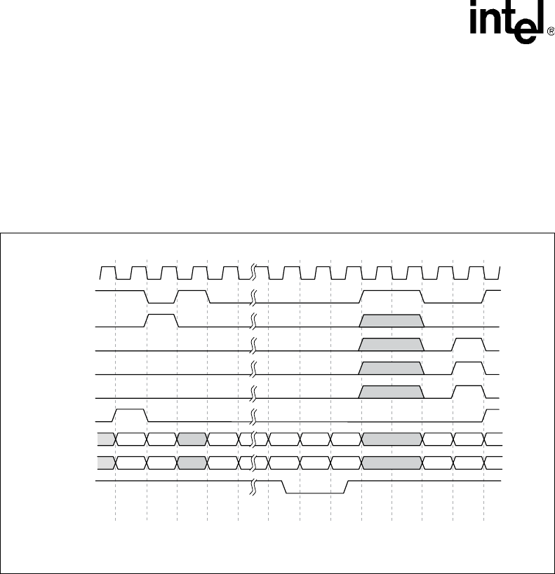
IXF1104 Quad-Port 10/100/1000 Mbps Ethernet Media Access Controller
84 Datasheet
Document Number: 278757
Revision Number: 007
Revision Date: March 25, 2004
5.2.2.1 Transmit Timing
In MPHY mode a packet transmission starts with the TSX signal indicating port address
information is on the data bus. The next clock cycle TENB and TSOP indicate present data on the
bus is the first word in the packet and all subsequent clocks will contain valid data as long as TENB
is active or until TEOP is asserted. Data transmission can be temporally halted when TENB goes
high then resumed when TENB is low. The valid bytes in the final word, during an active TEOP,
are indicated by state of TMOD [1:0].
5.2.2.2 Receive Timing
A packet is received when RSX indicates port address information on the data bus followed by
RSOP to indicate the data bus contains the first word of a packet. All subsequent data is valid only
while RVAL is High and until REOP is asserted. Receive data can be temporarily halted when
RENB is de-asserted and starts again on the second rising edge of RFCLK following the assertion
of RENB. RMOD indicates the number of valid bytes in the last transfer when REOP is asserted.
Figure 11. MPHY Transmit Logical Timing
B3216-01
TFCLK
TENB
TSOP
TEOP
TMOD[1:0]
TERR
TSX
TDAT[31:0]
TPRTY
TPA
0000 B1-B4 B5-B8 B41-B44 B45-B48 B49-B52 B53-B56 B57 B0001
1
1. Applies to all transmit packet available signals (STPA, PTPA, DTPA_0:3).
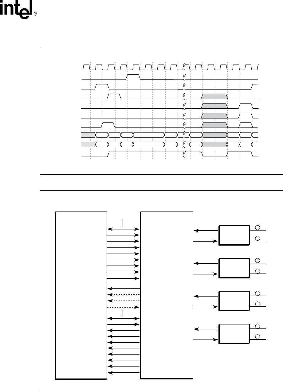
IXF1104 Quad-Port 10/100/1000 Mbps Ethernet Media Access Controller
Datasheet 85
Document Number: 278757
Revision Number: 007
Revision Date: March 25, 2004
Figure 12. MPHY Receive Logical Timing
Figure 13. MPHY 32-Bit Interface
B3217-01
TFCLK
RENB
RSX
RSOP
REOP
RERR
RMOD[1:0]
RDAT[31:0]
RPRTY
RVAL
0000 B1-B4 B5-B8 B9-B12 B13-B16 B45-B48 B52-B55 B56-B57 B0001
B0660-02
TFCLK
TENB
TDAT[31:0]
TPRTY
TERR
TSX
TSOP
TEOP
Network Processor SPI3 Bus IXF1104 MPHY
Mode
Transceiver
TFCLK
TENB_0
TDAT[31:0]
TPRTY_0
TMOD[1:0] TMOD[1:0]
RMOD[1:0] RMOD[1:0]
TERR_0
TSX
TSOP_0
TEOP_0
RFCLK
RENB
RDAT[31:0]
RPRTY RPRTY
RVAL
RERR
RSX
RSOP
REOP
RPRTY_0
RFCLK
RENB_0
RDAT[31:0]
RVAL_0
RERR_0
RSX
RSOP_0
REOP_0
DTPA_0:3
STPA
PTPA
TADR[1:0]
DTPA_0:3
STPA
PTPA
TADR[1:0]
Transceiver
Transceiver
Transceiver
Line-Side Interface
Port 0
Port 1
Port 3
Port 2

IXF1104 Quad-Port 10/100/1000 Mbps Ethernet Media Access Controller
86 Datasheet
Document Number: 278757
Revision Number: 007
Revision Date: March 25, 2004
5.2.2.3 Clock Rates
In MPHY mode, the TFCLK and RFCLK can be independent of each other. TFCLK and RFCLK
should be common to the IXF1104 and the Network Processor. The IXF1104 requires a single
clock source for the transmit path and a single clock source for the receive path.
To allow all four IXF1104 ports to operate at 1 Gbps, the IXF1104 is designed to allow this
interface to be overclocked. This allows operation for data transfer at data rates of up to 4.256 Gbps
when operating at an overclocked frequency of 133 MHz.
Note: MPHY mode operates at a maximum clock frequency of 133 MHz (TFCLK and RFCLK).
5.2.2.4 Parity
The IXF1104 can be odd or even (the IXF1104 is odd by default) when calculating parity on the
data bus. This can be changed to accommodate even parity if desired, and can be set for transmit
and receive independently. The RX Parity is set in bit 12 of the “SPI3 Receive Configuration
($0x701)” and the TX Parity is set in bit 4 of the “SPI3 Transmit and Global Configuration
($0x700)”.
5.2.2.5 SPHY Mode
The SPHY operation mode is selected when bit 21 of the Table 146 “SPI3 Transmit and Global
Configuration ($0x700)” on page 212 is set to 1. The SPHY mode is the default operation for the
IXF1104 SPI3 interface.
5.2.2.5.1 Data Path
The IXF1104 SPI3 interface has four 8-bit data paths that can support four independent 8-bit point-
to-point connections in SPHY mode (see Figure 16). Since each MAC port has its own dedicated
8-bit SPI3 data bus, each port has it own status signal (unlike MPHY). See the For a detailed list of
all the signals refer to the SPI3 pin multiplexing table....
Furthermore since each port has it own dedicated bus the in band port addressing is not needed.
The 8 bit data bus eliminates the need to have separate control signals determine the number of
valid bytes on an EOP.Therefore TSX, RSX, TMOD[1:0] RMOD[1:0] are not used in SPHY mode.
Note: See Table 17 “SPI3 MPHY/SPHY Interface” on page 58 for a complete list of the SPHY mode
signals. Unlike MPHY mode, each port has a dedicated control signal associated with each of the
per-port 8-bit data buses. Table 3 “SPI3 Interface Signal Descriptions” on page 38 provides signal
descriptions for all SPI3 signals.
5.2.2.5.2 Receive Data Transmission
Packets are transmitted on each port as they become available from the RX FIFO. The burst length
is determined by the setting of per port burst size and the B2B pause settings in the “SPI3 Receive
Configuration ($0x701)". If the B2B pause setting is zero pause cycles inserted, then the entire
packet will be burst without any pauses unless the Network Processor de-asserts RENB. If the
B2B_Pause setting calls for the insertion of two pause cycles on a port, these are inserted after each
data burst for that port. The data bursts are user configurable for each port in the “SPI3 Receive
Configuration ($0x701)".
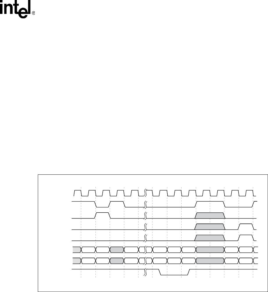
IXF1104 Quad-Port 10/100/1000 Mbps Ethernet Media Access Controller
Datasheet 87
Document Number: 278757
Revision Number: 007
Revision Date: March 25, 2004
5.2.2.6 SPHY Logical Timing
SPI3 interface AC timing for SPHY can be found in Section 7.2, “SPI3 AC Timing Specifications”
on page 136. Logical timing in the following diagrams illustrates all signals associated with SPHY
mode. SPHY mode is similar to MPHY mode except the following signals are not used:
•TMOD[1:0]
•RMOD[1:0]
•TSX
•RSX
•Address Data appearing on the data bus
5.2.2.7 Transmit Timing (SPHY)
Packet transmission starts when TENB and TSOP indicate present data on the bus is the first word
in the packet. All subsequent clocks will contain valid data as long as TENB is active or until
TEOP is asserted. Data transmission can be temporally halted when TENB goes high then resumed
when TENB is low.
5.2.2.8 Receive Timing (SPHY)
A packet is received when RSOP is asserted to indicate the data bus contains the first word of the
packet. All subsequent data is valid only while RVAL is high and until REOP is asserted. Receive
data can be temporarily halted when RENB is de-asserted and starts again on the second rising
edge of RFCLK following the assertion of RENB. When REOP is asserted RMOD indicates the
number of valid bytes in the last transfer.
Figure 14. SPHY Transmit Logical Timing
B3249-01
TFCLK
TENB
TSOP
TEOP
TERR
TDAT[7:0]_n
TPRTY
DTPA_n
B1 B2 B3 B60 B61 B62 B63 B64
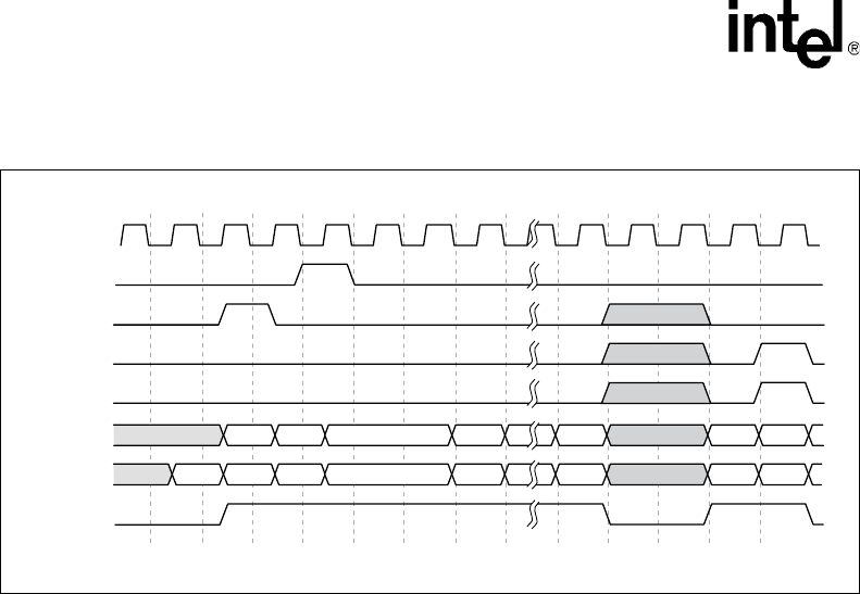
IXF1104 Quad-Port 10/100/1000 Mbps Ethernet Media Access Controller
88 Datasheet
Document Number: 278757
Revision Number: 007
Revision Date: March 25, 2004
Figure 15. SPHY Receive Logical Timing
B3250-01
RFCLK
RENB
RSOP
REOP
RERR
RDAT[7:0]_n
RPRTY
RVAL
B1 B2 B3 B4 B62 B63 B64
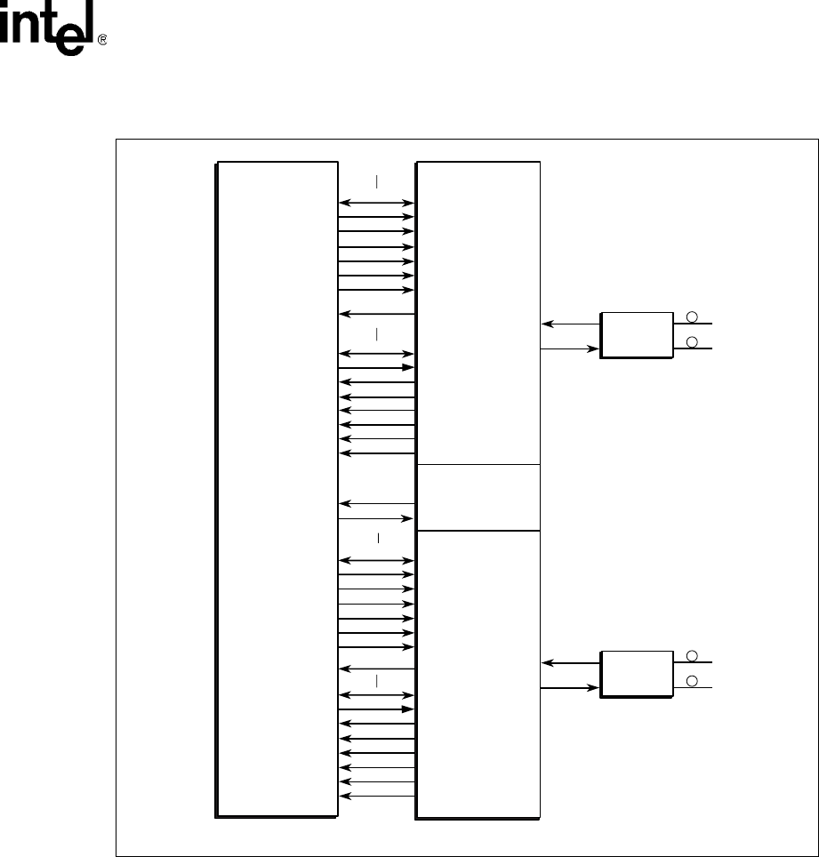
IXF1104 Quad-Port 10/100/1000 Mbps Ethernet Media Access Controller
Datasheet 89
Document Number: 278757
Revision Number: 007
Revision Date: March 25, 2004
5.2.2.8.1 Clock Rates
The TFCLK and RFCLK can be independent of each other in SPHY mode operation. TFCLK and
RFCLK should be common to all the Network Processor devices. The IXF1104 requires an
individual single clock source for the device transmit path and a single clock source for the device
receive path.
The IXF1104 allows this interface to be overclocked so that all four IXF1104 ports can operate at
1 Gbps. This allows data transfer at data rates of up to 4.0 Gbps when operating at an overclocked
frequency of 125 MHz.
Note: SPHY operates at a maximum frequency of 125Mhz.
Figure 16. SPHY Connection for Two IXF1104 Ports (8-Bit Interface)
B0659-02
TFCLK
TENB[0]
TDAT[7:0][0]
TPRTY[0]
TERR[0]
TSOP[0]
TEOP[0]
Network Processor SPI3 Bus Intel
®
IXF1104
Port 0
TFCLK
TENB_0
TDAT[7:0]_0
TPRTY_0
TERR_0
TSOP_0
TEOP_0
RFCLK
RENB[0]
RDAT[7:0][0]
RPRTY[0] RPRTY_0
RVAL[0]
RERR[0]
RSOP[0]
REOP[0]
RFCLK
RENB_0
RDAT[7:0]_0
RVAL_0
RERR_0
RSOP_0
REOP_0
DTPA[0]
TFCLK
TENB[1]
TDAT[7:0][1]
TPRTY[1]
TERR[1]
TSOP[1]
TEOP[1]
RFCLK
RENB[1]
RDAT[7:0][1]
RPRTY[1] RPRTY_1
RVAL[1]
RERR[1]
RSOP[1]
REOP[1]
DTPA[1]
DTPA_0
Transceiver
Port 1
SPI3
Flow Control
TFCLK
TENB_1
TDAT[7:0]_1
TPRTY_1
TERR_1
TSOP_1
TEOP_1
RFCLK
RENB_1
RDAT[7:0]_1
RVAL_1
RERR_1
RSOP_1
REOP_1
DTPA_1
Transceiver
Port 0
Port 1
Line-Side
Interface
Line-Side
Interface
PTPA
TADR[1:0]
PTPA
TADR[1:0]

IXF1104 Quad-Port 10/100/1000 Mbps Ethernet Media Access Controller
90 Datasheet
Document Number: 278757
Revision Number: 007
Revision Date: March 25, 2004
5.2.2.8.2 Parity
The IXF1104 can be odd or even (the IXF1104 defaults to odd) when calculating parity on the data
bus. This can be changed to accommodate even parity if desired, and can be set for transmit and
receive ports independently. The RX and TX parity sense bits have a direct relationship to the port
parity in SPHY mode.
The per port RX parity is set in the “SPI3 Receive Configuration ($0x701)" and the per port TX
Parity is set in the “SPI3 Transmit and Global Configuration ($0x700)".
5.2.2.9 SPI3 Flow Control
The SPI3 packet interface supports transmit and receive data transfers at clock rates independent of
the line bit rate. As a result, the IXF1104 supports packet rate decoupling using internal FIFOs.
These FIFOs are 10 KB per port in the transmit direction (egress from the IXF1104 to the line
interfaces) and 32 KB per port in the receive direction (ingress to the IXF1104 from the line
interfaces).
Control signals are provided to the network processor and the IXF1104 to allow either one to
exercise flow control. Since the bus interface is point-to-point, the receive interface of the IXF1104
pushes data to the link-layer device. For the transmit interface, the packet available status
granularity is byte-based.
5.2.2.9.1 RX SPI3 Flow Control
In the receive direction, when the IXF1104 has stored an end-of-packet (a complete small packet or
the end of a larger packet) or some predefined number of bytes in its receive FIFO, it sends the in-
band address followed by FIFO data to the link-layer device (in MPHY mode). The data on the
interface bus is marked with the valid signal (RVAL) asserted. The network processor device can
pause the data flow by de-asserting the Receive Read Enable (RENB) signal.
RENB_0:3
RENB_0:3 controls the flow of data from the IXF1104 RX FIFOs. In SPHY mode, there is a
dedicated RENB for each port. In MPHY mode, RENB_0 is used as the global signal covering all
ports. When RENB is sampled Low, the network processor can accept data. A read is performed
from the RX FIFO and the RDAT, RPRTY, RMOD[1:0], RSOP, REOP, RERR, RSX, and RVAL
signals are updated on the following rising edge of RFCLK.
RENB can be asserted High by the Network Processor at any time if it is unable to accept any more
data. When the RENB is sampled High by the IXF1104, a read of the RX FIFO is not performed,
and the RDAT, RPRTY, RMOD[1:0], RSOP, REOP, RERR, RSX and RVAL signals remain
unchanged on the following rising edge of RFCLK.
5.2.2.9.2 TX SPI3 Flow Control
In the transmit direction, when the IXF1104 has space for some predefined number of bytes in its
transmit FIFO, it informs the Network Processor device by asserting one of the Transmit Packet
Available (TPA) signals. The Network Processor device writes the in-band address followed by
packet data to the IXF1104 using an enable signal (TENB). The network processor device monitors
the TPA signals for a High-to-Low transition, which indicates that the transmit FIFO is almost full
(the number of bytes left in the FIFO is user-selectable by setting the “TX FIFO High Watermark
Ports 0 - 3 ($0x600 – 0x603)", and suspends data transfer to avoid an overflow. The Network
Processor device can pause the data flow by de-asserting the enable signal (TENB).

IXF1104 Quad-Port 10/100/1000 Mbps Ethernet Media Access Controller
Datasheet 91
Document Number: 278757
Revision Number: 007
Revision Date: March 25, 2004
The IXF1104 provides the following three types of TPA signals:
•Dedicated per port Direct Transmit Packet Available (DTPA)
•Selected-PHY Transmit Packet Available (STPA), which is based on the current in-band port
address in MPHY mode.
•Polled-PHY Transmit packet Available (PTPA), which provides FIFO information on the port
selected by the TADR[1:0] signals.
The following three TPA signals (DTPA_0:3, STPA, and PTPA) provide flow control based on the
programmable TX FIFO High and Low watermarks. Refer to Table 132 “TX FIFO High
Watermark Ports 0 - 3 ($0x600 – 0x603)” on page 202 and Table 133 “TX FIFO Low Watermark
Register Ports 0 - 3 ($0x60A – 0x60D)” on page 203 for more information.
DTPA_0:3:
A direct status indication for the TX FIFOs of ports [0:3]. When DTPA is High, it indicates the
amount of data in the TX FIFO is below the TX FIFO High watermark. When the High watermark
is crossed, DTPA transitions Low to indicate the TX FIFO is almost full. It stays low until the
amount data in the TX FIFO goes back below the TX FIFO Low watermark. At this point, DTPA
transitions High to indicate the programmed number of bytes are now available for data transfers.
DTPA_0:3 is updated on the rising edge of the TFCLK.
STPA:
STPA provides TX FIFO status for the currently selected port in MPHY mode. When High, STPA
indicates that the amount of data in the TX FIFO for the port selected, specified by the latest in-
band address, is below the TX FIFO High watermark. When the High watermark is crossed, STPA
transitions Low to indicate the TX FIFO is almost full. It stays Low until the amount of data in the
TX FIFO goes back below the TX FIFO Low watermark. At this point, STPA transitions High to
indicate the programmed number of bytes are now available for data transfers.
The port reported by STPA is updated on the rising edge of TFCLK after TSX is sampled as
asserted. STPA is updated on the rising edge of TFCLK.
Note: STPA is only used when the IXF1104 is configured for MPHY mode of operation.
PTPA:
PTPA provides status of the TX FIFO based on the port selected by the TADR[1:0] address bus.
When High, PTPA indicates that the amount of data in the TX FIFO for the port selected is below
the TX FIFO High watermark. When the High watermark is crossed, PTPA transitions Low to
indicate the TX FIFO is almost full. It stays Low until the amount of data in the TX FIFO goes
back below the TX FIFO Low watermark. PTPA then transitions High to indicate the programmed
number of bytes are now available for data transfers.
The port reported by PTPA is updated on the rising edge of TFCLK after the TADR{1:0] port
address is sampled.
PTPA is updated on the rising edge of TFCLK.

IXF1104 Quad-Port 10/100/1000 Mbps Ethernet Media Access Controller
92 Datasheet
Document Number: 278757
Revision Number: 007
Revision Date: March 25, 2004
5.2.3 Pre-Pending Function
The IXF1104 implements a pre-pending feature to allow 1518-byte Ethernet packets to be pre-
padded with two additional bytes of data so that the packet becomes low-word aligned. The 2-byte
pre-pend value is all zeros and is inserted before the destination address of the packet being pre-
pended. This value is fixed and cannot be changed.
This function is enabled by writing the appropriate data to the “RX FIFO Padding and CRC Strip
Enable ($0x5B3)" for each port.
A standard 1518-byte Ethernet packet occupies 379 long words (four bytes) with two additional
bytes left over (1518/4 = 379.5). To eliminate the memory-management problems for a network
processor or switch fabric, the two remaining bytes are dealt with by the addition of two bytes to
the start of a packet. This results in a standard 1518-byte Ethernet packet received by the IXF1104
being forwarded to the higher-layer device as a 380-long-word packet. The upper-layer device is
responsible for stripping the additional two bytes.
This feature was added to the IXF1104 to assist in the design of higher-layer memory management.
The addition of the two extra bytes is not the default operation of the IXF1104 and must be enabled
by the user. The default operation of the IXF1104 SPI3 receive interface forwards data exactly as it
is received by the IXF1104 line interface.
5.3 Gigabit Media Independent Interface (GMII)
The IXF1104 supports a subset of the GMII interface standard as defined in IEEE 802.3 2000
Edition for 1 Gbps operation only. This subset is limited to operation at 1000 Mbps full-duplex.
The GMII Interface operates as a source synchronous interface only and does not accept a TXC
clock provided by a PHY device when operating at 10/100 Mbps speeds.
Note: The RGMII interface must be used for applications that require 10/100/1000 Mbps operation.
The IXF1104 does NOT support 10/100 Mbps copper PHY devices that are implemented using the
MII Interface.
Note: MII operation is not supported by the IXF1104.
The user can select GMII, RGMII, or Optical Module/SerDes functionality on a per-port basis.
This mode of operation is controlled through a configuration register.
While IEEE 802.3 specifies 3.3 V operation of GMII devices, most PHYs use 2.5 V signaling. The
IXF1104 provides a 2.5 V drive and is 3.3 V-tolerant on inputs.
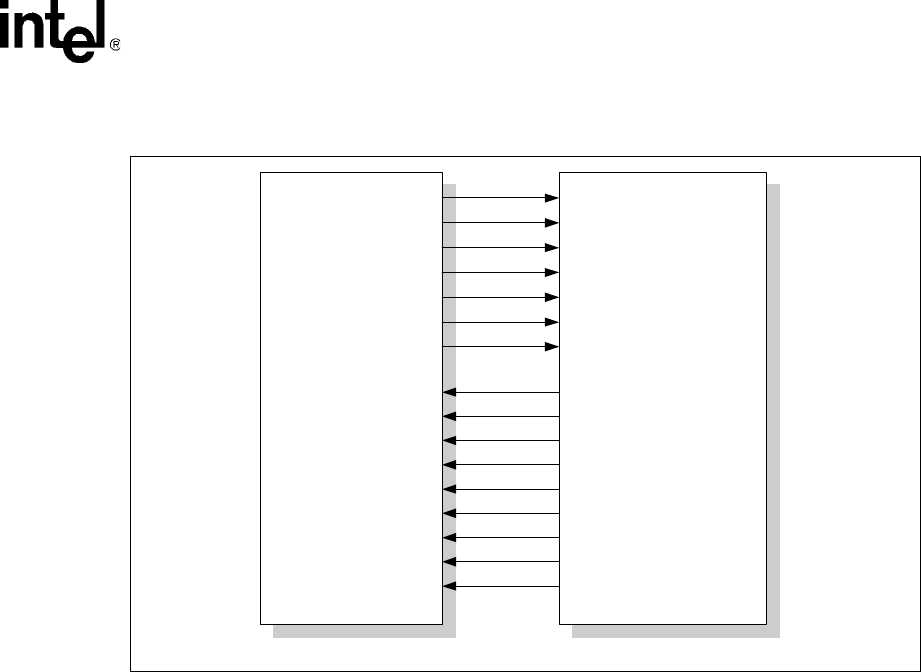
IXF1104 Quad-Port 10/100/1000 Mbps Ethernet Media Access Controller
Datasheet 93
Document Number: 278757
Revision Number: 007
Revision Date: March 25, 2004
5.3.1 GMII Signal Multiplexing
The GMII balls are reassigned when using the RGMII mode or fiber mode. Table 16 “Line Side
Interface Multiplexed Balls” on page 57 specifies the multiplexing of GMII balls in these modes.
See Section 5.1.3, “Mixed-Mode Operation” on page 74 for proper configuration of the IXF1104 in
GMII mode.
5.3.2 GMII Interface Signal Definition
Table 26 “GMII Interface Signal Definitions” on page 94 provides the GMII interface signal
definitions. For information on 1000BASE-T GMII transmit and receive timing diagrams and
tables, please refer to Table 49 “GMII 1000BASE-T Transmit Signal Parameters” on page 141,
Figure 38 “1000BASE-T Transmit Interface Timing” on page 141, Figure 39 “1000BASE-T
Receive Interface Timing” on page 142, and Table 50 “GMII 1000BASE-T Receive Signal
Parameters” on page 142
Figure 17. MAC GMII Interconnect
TXC_3:0
TX_EN_3:0
TX_ER_3:0
RXC_3:0
TXD[7:0]_0
TXD[7:0]_3
TXD[7:0]_2
TXD[7:0]_1
RX_EN_3:0
RX_ER_3:0
RXD[7:0]_0
RXD[7:0]_3
RXD[7:0]_2
RXD[7:0]_1
COL_3:0
CRS_3:0
Intel® IXF1104
Media Access Controller
TXC_3:0
TX_EN_3:0
TX_ER_3:0
TXD[7:0]_0
TXD[7:0]_3
TXD[7:0]_2
TXD[7:0]_1
RXC_3:0
RX_EN_3:0
RX_ER_3:0
RXD[7:0]_0
RXD[7:0]_3
RXD[7:0]_2
RXD[7:0]_1
COL_3:0
CRS_3:0
Quad PHY Device
B3203-0
1

IXF1104 Quad-Port 10/100/1000 Mbps Ethernet Media Access Controller
94 Datasheet
Document Number: 278757
Revision Number: 007
Revision Date: March 25, 2004
Table 26. GMII Interface Signal Definitions
IXF1104
Signal GMII Standard
Signal Source Description
TXC_0
TXC_1
TXC_2
TXC_3
GTX_CLK IXF1104
Transmit Reference Clock:
125 MHz for Gigabit operation.
MII operation for 10/100 Mbps operation is not
supported.
TXD[7:0]_0
TXD[7:0]_1
TXD[7:0]_2
TXD[7:0]_3
TXD[7:0] IXF1104
Transmit Data Bus:
Width of this synchronous output bus varies with the
speed/mode of operation. In 1000 Mbps mode, all 8
bits are used.
TX_EN_0
TX_EN_1
TX_EN_2
TX_EN_3
TX_EN IXF1104
Transmit Enable:
Synchronous input that indicates Valid data is being
driven on the TXD[7:0] data bus.
TX_ER_0
TX_ER_1
TX_ER_2
TX_ER_3
TX_ER IXF1104
Transmit Error:
Synchronous input to PHY causes the transmission of
error symbols in 1000 Mbps links.
RXC_0
RXC_1
RXC_2
RXC_3
RX_CLK PHY Receive Clock:
Continuous reference clock is 125 MHz +/– 100 ppm.
RXD[7:0]_0
RXD[7:0]_1
RXD[7:0]_2
RXD[7:0]_3
RXD<3:0> PHY
Receive Data Bus:
Width of the bus varies with the speed and mode of
operation. In 1000 Mbps mode, all 8 bits are driven by
the PHY device.
Note: MII operation at 10/100 Mbps is not supported.
RX_DV_0
RX_DV_1
RX_DV_2
RX_DV_3
RX_DV PHY
Receive Data Valid:
This signal is asserted when valid data is present on
the corresponding RXD bus.
RX_ER_0
RX_ER_1
RX_ER_2
RX_ER_3
RX_ER PHY
Receive Error:
In 1000 Mbps mode, asserted when error symbols or
carrier extension symbols are received.
Always synchronous to RX_CLK.
CRS_0
CRS_1
CRS_2
CRS_3
CRS PHY
Carrier Sense:
Asserted when valid activity is detected at the line-
side interface.
COL_0
COL_1
COL_2
COL_3
COL PHY
Collision:
Asserted when a collision is detected and remains
asserted for the duration of the collision event. In full-
duplex mode, the PHY should force this signal Low.
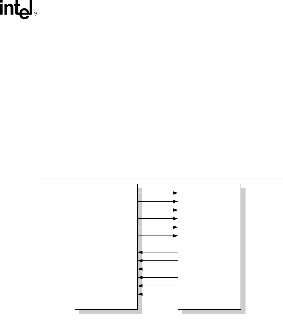
IXF1104 Quad-Port 10/100/1000 Mbps Ethernet Media Access Controller
Datasheet 95
Document Number: 278757
Revision Number: 007
Revision Date: March 25, 2004
5.4 Reduced Gigabit Media Independent Interface (RGMII)
The IXF1104 supports the RGMII interface standard as defined in the RGMII Version 1.2
specification. The RGMII interface is an alternative to the IEEE 802.3u MII interface.
The RGMII interface is intended as an alternative to the IEEE 802.3u MII and the IEEE 802.3z
GMII. The principle objective of the RGMII is to reduce the number of balls (from a maximum of
28 balls to 12 balls) required to interconnect the MAC and the PHY. This reduction is both cost-
effective and technology-independent. To accomplish this objective, the data paths and all
associated control signals are reduced, control signals are multiplexed together, and both edges of
the clock are used.
•1000 Mbps operation – clocks operate at 125 MHz
•100 Mbps operation – clocks operate at 25 MHz
•10 Mbps operation – clocks operate at 2.5 MHz.
Note: The IXF1104 RGMII interface is multiplexed with signals from the GMII interface. See Table 16
“Line Side Interface Multiplexed Balls” on page 57 for detailed information.
5.4.1 Multiplexing of Data and Control
Multiplexing of data and control information is achieved by utilizing both edges of the reference
clocks and sending the lower four bits on the rising edge and the upper four bits on the falling edge.
Control signals are multiplexed into a single clock cycle using the same technique. For further
information on timing parameters, see Figure 37 “RGMII Interface Timing” on page 140 and
Table 48 “RGMII Interface Timing Parameters” on page 140.
Figure 18. RGMII Interface
TXC_3:0
TX_CTL_3:0
TXD[3:0]_3
TXD[3:0]_0
TXD[3:0]_1
TXD[3:0]_2
Intel® IXF1104
Media Access Controller
TXC_3:0
Quad PHY Device
B3203-0
1
TX_CTL_3:0
TXD[3:0]_3
TXD[3:0]_0
TXD[3:0]_1
TXD[3:0]_2
RXC_3:0
RX_CTL_3:0
RXD[3:0]_3
RXD[3:0]_0
RXD[3:0]_1
RXD[3:0]_2
RXC_3:0
RX_CTL_3:0
RXD[3:0]_3
RXD[3:0]_0
RXD[3:0]_1
RXD[3:0]_2

IXF1104 Quad-Port 10/100/1000 Mbps Ethernet Media Access Controller
96 Datasheet
Document Number: 278757
Revision Number: 007
Revision Date: March 25, 2004
5.4.2 Timing Specifics
The IXF1104 RGMII complies with RGMII Rev1.2a requirements. Table 27 provides the timing
specifics.
5.4.3 TX_ER and RX_ER Coding
To reduce interface power, the transmit error condition (TX_ER) and the receive error condition
(RX_ER) are encoded on the RGMII interface to minimize transitions during normal network
operation (refer to Table 28 on page 96 for the encoding method). Table 27 provides signal
definitions for RGMII.
The value of RGMII_TX_ER and RGMII_TX_EN are valid at the rising edge of the clock while
TX_ER is presented on the falling edge of the clock. RX_ER coding behaves in the same way (see
Table 28, Figure 19, and Figure 20).
Table 27. RGMII Signal Definitions
IXF1104
Signal
RGMII
Standard
Signal Source Description
TXC_0:3 TXC MAC Depending on speed, the transmit reference clock is 125 MHz, 25 MHz,
or 2.5 MHz +/– 50ppm.
TD[3:0]_nTD<3:0> MAC Contains register bits 3:0 on the rising edge of TXC and register bits 7:4
on the falling edge of TXC.
TX_EN TX_CTL MAC TXEN is on the leading edge of TXC.
TX_EN xor TX_ER is on the falling edge of TXC.
RXC_0:3 RXC PHY Continuous reference clock is 125 MHz, 25 MHz, or 2.5 MHz +/– 50
ppm.
RD[3:0]_nRD<3:0> PHY Contains register bits 3:0 on the leading edge of RXC and register bits
7:4 on the trailing edge of RXC.
RX_DV RX_CTL PHY RX_DV is on the leading edge of RXC.
RX_DV or RXERR is the falling edge of RXC.
Table 28. TX_ER and RX_ER Coding Description
Condition Description
Receiving valid frame,
no errors RX_DV = true
Logic High on rising edge of RXC RX_ER = false
Logic High on the falling edge of RXC
Receiving valid frame,
with errors RX_DV = true
Logic High on rising edge of RXC RX_ER = true
Logic Low on the falling edge of RXC
Receiving invalid frame
(or no frame) RX_DV = false
Logic Low on rising edge of RXC RX_ER = false
Logic Low on the falling edge of RXC
Transmitting valid frame,
no errors
TX_EN = true
Logic High on rising edge of TXC
TX_ER =false
Logic High on the falling edge of TXC
Transmitting valid frame
with errors
TX_EN = true
Logic High on rising edge of TXC
TX_ER = true
Logic Low on the falling edge of TXC
Transmitting invalid
frame (or no frame)
TX_EN = false
Logic Low on rising edge of TXC
TX_ER = false
Logic low on the falling edge of TXC
NOTE: Refer to Figure 19 for TX_CTL behavior, and Figure 20 for RX_CTL behavior.
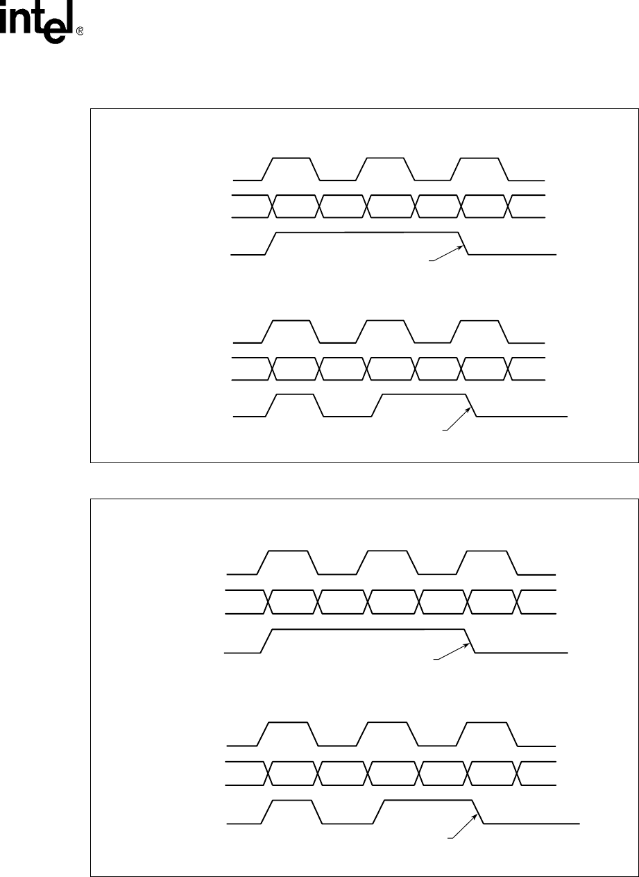
IXF1104 Quad-Port 10/100/1000 Mbps Ethernet Media Access Controller
Datasheet 97
Document Number: 278757
Revision Number: 007
Revision Date: March 25, 2004
Figure 19. TX_CTL Behavior
Figure 20. RX_CTL Behavior
B0616-02
TXC_0:3
(at Transmitter)
TD[3:0]_0:3
TX_CTL_0:3
End-of-Frame
TD[3:0] TD[7:4]
TX_EN=True TX_ER=False TX_EN=False TX_ER=False
TXC_0:3
(at Transmitter)
TD[3:0]_0:3
TX_CTL_0:3
End-of-Frame
TD[3:0] TD[7:4]
TX_EN=True TX_ER=False TX_EN=False TX_ER=False
Valid Frame
Frame with Error
B3237-01
RXC_0:3
(at PHY)
RD[3:0]_0:3
RX_CTL_0:3
End-of-Frame
RD[3:0] RD[7:4]
RX_DV=True RX_ER=False RX_DV=False RX_ER=False
RXC_0:3
(at PHY)
RD[3:0]_0:3
RX_CTL_0:3
End-of-Frame
RD[3:0] RD[7:4]
RX_DV=True RX_ER=True RX_DV=False RX_ER=False
Valid Frame
Frame with Error

IXF1104 Quad-Port 10/100/1000 Mbps Ethernet Media Access Controller
98 Datasheet
Document Number: 278757
Revision Number: 007
Revision Date: March 25, 2004
5.4.3.1 In-Band Status
Carrier Sense (CRS) is generated by the PHY when a packet is received from the network
interface. CRS is indicated when:
•RXDV = true.
•RXDV = false, RXERR = true, and a value of FF exists on the RXD[7:0] bits simultaneously.
•Carrier Extend, Carrier Extend Error, or False Carrier occurs (please reference the Hewlett-
Packard* Version 1.2a RGMII Specification for details.).
Carrier Extend and Carrier Extend Error are applicable to Gigabit speeds only. Collision is
determined at the MAC by the assertion of TXEN being true while either CRS or RXDV are true.
The PHY will not assert CRS as a result of TXEN being true.
5.4.4 10/100 Mbps Functionality
The RGMII interface implements the 10/100 Mbps Ethernet Media Independent Interface (MII) by
reducing the clock rate to 25 MHz for 100 Mbps operation and 2.5 MHz for 10 Mbps. The TXC is
generated by the MAC and the RXC is generated by the PHY. During packet reception, the RXC is
stretched on either the positive or negative pulse to accommodate transition from the free-running
clock to a data-synchronous clock domain. When the speed of the PHY changes, a similar
stretching of the positive or negative pulses is allowed. No glitching of the clocks is allowed during
speed transitions.
This interface operates at 10 Mbps and 100 Mbps speeds in the same manner as 1000 Mbps speed,
although the data may be duplicated on the falling edge of the appropriate clock. The MAC holds
TX_CTL Low until it is operating at the same speed as the PHY.
Note: The IXF1104 does not support 10/100 Mbps operation when configured in GMII mode
5.5 MDIO Control and Interface
The IXF1104 supports the IEEE 802.3 MII Management Interface, also known as the Management
Data Input/Output (MDIO) Interface. This interface allows the IXF1104 to monitor and control
each of the PHY devices that are connected to the four ports of IXF1104 when those ports are in
copper mode.
The MDIO Master Interface block is implemented once in the IXF1104. The MDIO Interface block
contains the logic through which the user accesses the registers in PHY devices connected to the
MDIO/MDC interface, which is controlled by each port.
The MDIO Master Interface block supports the management frame format, specified by IEEE
802.3, clause 22.2.4.5. This block also supports single MDI access through the CPU interface and
an autoscan mode. Autoscan allows the MDIO master to read all 32 registers of the per-port copper
PHYs and store the contents in the IXF1104. This provides external-CPU-ready access to the PHY
register contents through a single CPU read without the latency of waiting on the low-speed serial
MDIO data bus for each register access.
Scan of a single register with low-frequency operation takes approximately 25.6 µs. Scan of a 32-
register block takes approximately 820 µs, or 3.3 ms for all four ports. Autoscan data is not valid
until approximately 19.2 µs after enabling scan. These numbers scale by 7/50 for high-frequency
operation.

IXF1104 Quad-Port 10/100/1000 Mbps Ethernet Media Access Controller
Datasheet 99
Document Number: 278757
Revision Number: 007
Revision Date: March 25, 2004
5.5.1 MDIO Address
The 5-bit PHY address for the MDIO transactions can be set in the “MDIO Single Command
($0x680)". Bits 5:2 of the PHY address are fixed to a value of 0. Bits 1 and 0 are programmable in
bits 9 and 8 of “MDIO Single Command ($0x680)".
5.5.2 MDIO Register Descriptions
For complete information on the MDI registers, refer to the Table 142 “MDIO Single Command
($0x680)” on page 210, Table 143 “MDIO Single Read and Write Data ($0x681)” on page 210,
Table 144 “Autoscan PHY Address Enable ($0x682)” on page 211, and Table 145 “MDIO Control
($0x683)” on page 211.
5.5.3 Clear When Done
The MDI Command register bit, in the “MDIO Single Command ($0x680)", clears upon command
completion and is set by the user to start the requested single MDIO Read or Write operation. This
bit is cleared automatically upon operation completion.
5.5.4 MDC Generation
The MDC clock is used for the MDIO/MDC interface. The frequency of the MDC clock is
selectable by setting bit 0, MDC Speed, in an IXF1104 configuration register (see Table 145
“MDIO Control ($0x683)” on page 211).
5.5.4.1 MDC High-Frequency Operation
The high-frequency MDC is 18 MHz, derived from the 125-MHz system clock by dividing the
frequency by 7.
The duty cycle is as follows:
•MDC High duration: 3 x (1/125 MHz) = 3 x 8 ns = 24 ns
•MDC Low duration: 4 x (1/125 MHz) = 4 x 8 ns = 32 ns
•MDC runs continuously after reset
Refer to Figure 41 “MDC High-Speed Operation Timing” on page 144 for the high-frequency
MDC timing diagram.
5.5.4.2 MDC Low-Frequency Operation
The low-frequency MDC is 2.5 MHz, which is derived from the 125-MHz system clock by
dividing the frequency by 50.
The duty cycle is as follows:
•MDC High duration: 25 x (1/125 MHz) = 25 x 8 ns = 200 ns
•MDC Low duration: 25 x (1/125 MHz) = 25 x 8 ns = 200 ns
•MDC runs continuously after reset

IXF1104 Quad-Port 10/100/1000 Mbps Ethernet Media Access Controller
100 Datasheet
Document Number: 278757
Revision Number: 007
Revision Date: March 25, 2004
Refer to Figure 42 “MDC Low-Speed Operation Timing” on page 144 for the low frequency MDC
timing diagram.
5.5.5 Management Frames
The Management Interface serializes the external register access information into the format
specified by IEEE 802.3, Section 22.2.4.5 (see Figure 21).
5.5.6 Single MDI Command Operation
The Management Data Interface is accessed through the “MDIO Single Command ($0x680)" and
the “MDIO Single Read and Write Data ($0x681)". A single management frame is sent by setting
Register 0, bit 20 to logic 1, and is automatically cleared when the frame is completed.
The Write data is first set up in Register 1, bits 15:0 for Write operation. Register 0 is initialized
with the appropriate control information (start, op code, etc.) and Register 0, bit 20 is set to logic 1.
Register 0, bit 20 is reset to logic 0 when the frame is complete.
The steps are identical for Read operation except that in Register 1, bits 15:0, the data is ignored.
The data received from the MDIO is read by the CPU interface from Register 1, bits 31:16.
5.5.7 MDI State Machine
The MDI State Machine sequences the information sent to it by the MDIO control registers and
keeps track of the current sequence bit count, enabling or disabling the MDIO driver output (see
Figure 22.
Figure 21. Management Frame Structure (Single-Frame Format)
Preamble
32 Bits
Start
2 Bits Op Code
2 Bits PHY Addr
5 Bits Turnaround
2 Bits Data
16 Bits
First Bit Transmitted Last Bit Transmitted
REG Addr
5 Bits
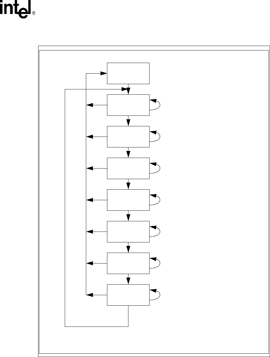
IXF1104 Quad-Port 10/100/1000 Mbps Ethernet Media Access Controller
Datasheet 101
Document Number: 278757
Revision Number: 007
Revision Date: March 25, 2004
Figure 22. MDI State
Idle
Preamble
Go = 1
Cnt = 32
Cnt < 32
Start Bits
Cnt = 2
Cnt < 2
Cnt > 32
Cnt > 2
Cnt > 2
Op Code
Phy Addr
Cnt = 2
Cnt < 2
Cnt > 5 Cnt < 5
Reg Addr
Cnt = 5
Cnt = 5
Cnt < 5
Cnt > 5
Turn Around
Cnt > 2 Cnt < 2
Cnt = 2
Data
Cnt < 16
Cnt > 16
Cnt = 16 And Go = 1
or (Cnt = 16 and
Go = 0)
MDOE = 0
MDO = 0
MDC_EN = 0
MDOE = 1
MDO = 1
MDC_EN = 1
MDOE = 1
MDO = Reg_Bit_St(Cnt)
MDC_EN = 1
MDOE = 1
MDO = Reg_Bit_Op(Cnt)
MDC_EN = 0
MDOE = 1
MDO = Reg_Bit_PA(Cnt)
MDC_EN = 1
MDOE = 1
MDO = Reg_Bit_RA(Cnt)
MDC_EN = 1
MDOE = Wr_Op
MDO = Reg_Bit_WO(Cnt)
MDC_EN = 1
MDOE = Wr_Op
MDO = Data(Cnt)
MDC_EN = 1

IXF1104 Quad-Port 10/100/1000 Mbps Ethernet Media Access Controller
102 Datasheet
Document Number: 278757
Revision Number: 007
Revision Date: March 25, 2004
5.5.8 Autoscan Operation
The autoscan function allows the 32 registers in each external PHY (up to four) to be stored
internally in the IXF1104. Autoscan is enabled by setting bit 1 of the MDI Control register. When
enabled, autoscan runs continuously, reading each PHY register. When a PHY register access is
instigated through the CPU interface, the current autoscan register Read is completed before the
CPU register access starts. Upon completion of the CPU-induced access, the autoscan functionality
restarts from the last autoscan register access.
The“Autoscan PHY Address Enable ($0x682)" determines which PHY addresses are being
occupied for each IXF1104 port. The least significant bit (LSB) that is set in the register is Port 0,
the next significant bit that is set is assumed to be port 1, and so on. If more than four bits are set,
the bits beyond the fourth bit are ignored. If less than four bits are set, the round-robin process
returns to the port identified by the LSB being set.
5.6 SerDes Interface
The IXF1104 integrates four integrated Serializer/Deserializer (SerDes) devices that allow direct
connection to optical modules and remove the requirement for external SerDes devices. This
increases integration, which reduces the size of the PCB area required to implement this function,
reduces total power, reduces silicon and manufacturing costs, and improves reliability. Each
SerDes interface is identical and fully compliant with the relevant IEEE 802.3 Specifications,
including auto-negotiation. Each port is also compliant with and supports the requirements of the
Small Form Factor Pluggable (SFP) Multi-Source Agreement (MSA), see Section 5.7, “Optical
Module Interface” on page 106.
The following sections describe the operations supported by each interface, the configurable
options, and the register bits that control these options. A full list of the register addresses and full
bit definitions are found in the register maps (Table 59 through Table 69).
5.6.1 Features
The SerDes cores are designed to operate in point-to-point data transmission applications. While
the core can be used across various media types, such as PCB or backplanes, it is configured
specifically for use in 1000BASE-X Ethernet fiber applications in the IXF1104. The following
features are supported.
•10-bit data path, which connects to the output/input of the 8B/10B encoder/decoder PCS that
resides in the MAC controller
•Data frequency of 1.25 GHz
•Low power: <200 mW per SerDes port
•Asynchronous clock data recovery
5.6.2 Functional Description
The SerDes transmit interface sends serialized data at 1.25 GHz. The interface is differential with
two signals for transmit operation. The transmit interface is designed to operate in a 100 Ω
differential environment and all the terminations are included on the device. The outputs are high-

IXF1104 Quad-Port 10/100/1000 Mbps Ethernet Media Access Controller
Datasheet 103
Document Number: 278757
Revision Number: 007
Revision Date: March 25, 2004
speed SerDes and are capable of operating in either an AC- or DC-coupled environment. AC
coupling is recommended for this interface to ensure that the correct input bias current is supplied
at the receiver.
The SerDes receive interface receives serialized data at 1.25 GHz. The interface is differential with
two signals for the receive operation. The equalizer receives a differential signal that is equalized
for the assumed media channel. The SerDes transmit and receive interfaces are designed to operate
within a 100 Ω differential environment and all terminations are included on the device. The
SerDes is capable of operating in either AC- or DC-coupled environments.
5.6.2.1 Transmitter Operational Overview
The transmit section of the IXF1104 has to serialize the Ten Bit Interface (TBI) data from the
IXF1104 MAC section and outputs this data at 1.25 GHz differential signal levels. The 1.25 GHz
differential SerDes signals are compliant with the Small Form Factor Pluggable (SFP) Multi-
Source Agreement (MSA).
The transmitter section takes the contents of the data register within the MAC and synchronously
transfers the data out, ten bits at a time – Least Significant Bit (LSB) first, followed by the next
Most Significant Bit (MSB). When these ten bits have been serialized and transmitted, the next
word of 10-bit data from the MAC is ready to be serialized for transmission.
The data is transmitted by the high-speed current mode differential SerDes output stage using an
internal 1.25 GHz clock generated from the 125 MHz clock input.
5.6.2.2 Transmitter Programmable Driver-Power Levels
The IXF1104 SerDes core has programmable transmitter power levels to enhance usability in any
given application.The SerDes Registers are programmable to allow adjustment of the transmit core
driver output power. When driving a 100 Ω differential terminated network, these output power
settings effectively establish the differential voltage swings at the driver output.
The “TX Driver Power Level Ports 0 - 3 ($0x784)" allows the selection of four discrete power
settings. The selected power setting of these inputs is applied to each of the transmit core drivers on
a per-port basis. Table 29 “SerDes Driver TX Power Levels” lists the normalized power settings of
the transmit drivers as a function of the Driver Power Control inputs. The normalized current
setting is 10 mA, which corresponds to the normalized power setting of 1.0. This is the default
setting of the IXF1104 SerDes interface. Other values listed in the Normalized Driver Power
Setting column are multiples of 10 mA. For example, with inputs at 1110, the driver power is the
following:
.5 x 10 mA = 5 mA.
Table 29. SerDes Driver TX Power Levels
DRVPWRx[3] DRVPWRx[2] DRVPWRx[1] DRVPWRx[0] Normalized
Driver Power
Setting Driver Power
0 0 1 1 1.33 13.3 mA
NOTE: All other values are reserved.

IXF1104 Quad-Port 10/100/1000 Mbps Ethernet Media Access Controller
104 Datasheet
Document Number: 278757
Revision Number: 007
Revision Date: March 25, 2004
5.6.2.3 Receiver Operational Overview
The receiver structure performs Clock and Data Recovery (CDR) on the incoming serial data
stream. The quality of this operation is a dominant factor for the Bit Error Rate (BER) system
performance. Feed forward and feedback controls are combined in one receiver architecture for
enhanced performance. The data is over-sampled and a digital circuit detects the edge position in
the data stream. A signal is not generated if an edge is not found. A feedback loop takes care of
low-frequency jitter phenomenon of unlimited amplitude, while a feed forward section suppresses
high-frequency jitter having limited amplitude. The static edge position is held at a constant
position in the over-sampled by a constant adjustment of the sampling phases with the early and
late signals.
5.6.2.4 Selective Power-Down
The IXF1104 offers the ability to selectively power-down any of the SerDes TX or RX ports that
are not being used. This is done via “TX and RX Power-Down ($0x787)” on page 219.
5.6.2.5 Receiver Jitter Tolerance
The SerDes receiver architecture is designed to track frequency mismatch, recover phase, and is
tolerant of low-frequency data jitter. Figure 23 specifies the SerDes core receiver sinusoidal jitter
tracking capabilities.
1 0 1 1 2.0 20 mA
1 1 0 1 1.0 10 mA
1110 0.5 5 mA
Table 29. SerDes Driver TX Power Levels
DRVPWRx[3] DRVPWRx[2] DRVPWRx[1] DRVPWRx[0] Normalized
Driver Power
Setting Driver Power
NOTE: All other values are reserved.
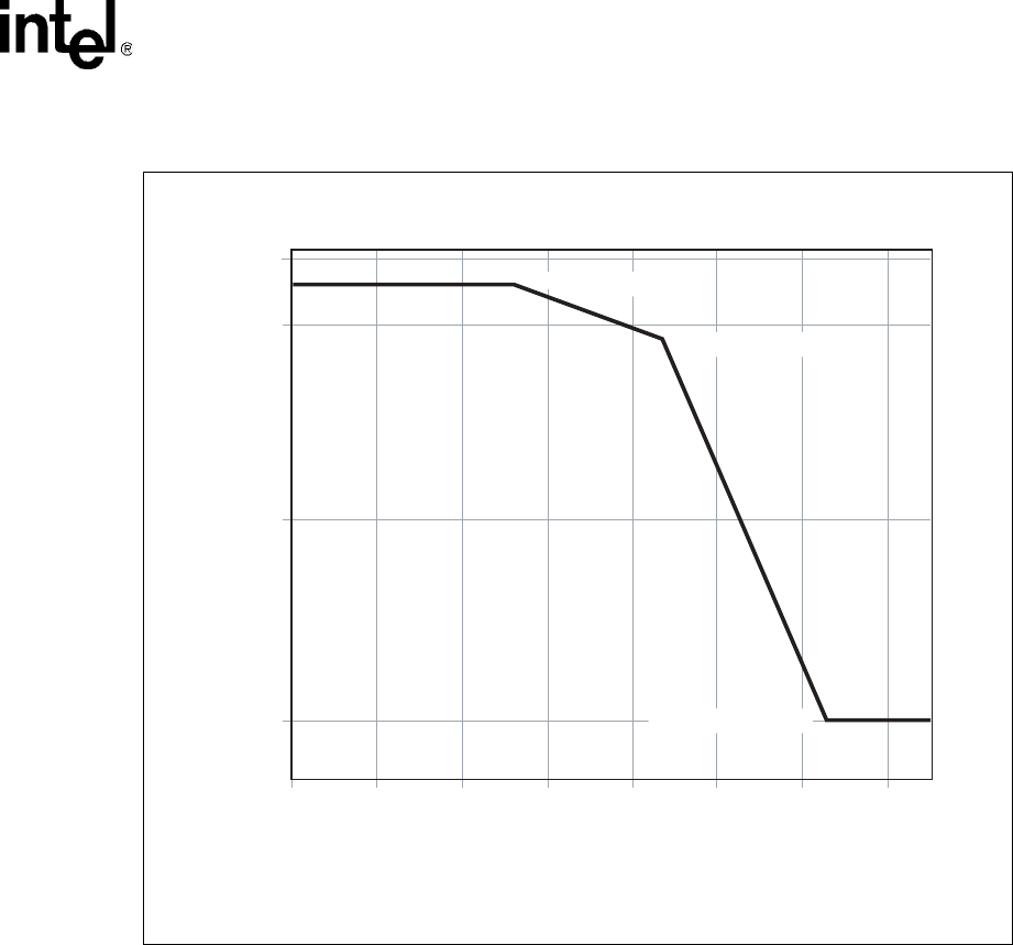
IXF1104 Quad-Port 10/100/1000 Mbps Ethernet Media Access Controller
Datasheet 105
Document Number: 278757
Revision Number: 007
Revision Date: March 25, 2004
5.6.2.6 Transmit Jitter
The SerDes core total transmit jitter, including contributions from the intermediate frequency PLL,
is comprised of the following two components:
•A deterministic component attributed to the SerDes core’s architectural characteristics
•A random component attributed to random thermal noise effects
Since the thermal noise component is random and statistical in nature, the SerDes core total
transmit jitter must be specified as a function of BER.
5.6.2.7 Receive Jitter
The SerDes core total receiver jitter, including contributions from the intermediate frequency PLL,
is comprised of the following two components:
•A deterministic component attributed to the SerDes core architectural characteristics
•A random component attributed to random thermal noise effects.
Figure 23. SerDes Receiver Jitter Tolerance
Note: UI = Unit interval.
B0745-02
10-1
0
10+1
10
0
10
1
10
2
10
3
10
4
10
5
10
6
10
7
Frequency
Sinusoidal Jitter Mask
Peak-to-Peak Amplitude (UI)
16 ui 375 Hz 16 ui
22.5836 kHz 8.5 ui
1.9195 MHz 0.1 ui

IXF1104 Quad-Port 10/100/1000 Mbps Ethernet Media Access Controller
106 Datasheet
Document Number: 278757
Revision Number: 007
Revision Date: March 25, 2004
5.7 Optical Module Interface
This section describes the connection of the IXF1104 ports to an Optical Module Interface and
details the minimal connections that are supported for correct operation. The registers used for
write control and read status information are documented.
The Optical Module Interface allows the IXF1104 a seamless connection to the Small Form Factor
Optical Modules (SFP) that form the system’s physical media connection, eliminating the need for
any FPGAs or CPUs to process data. All required optical module information is available to the
system CPU through the IXF1104 CPU interface, leading to a more integrated, reliable, and cost-
effective system.
The IXF1104 supports all the functions required for the Small Form Factor pluggable Multi-Source
Agreement (MSA).
There are specific mechanical and electrical requirements for the size, form factor, and connections
supported on all Optical Module Interfaces. There are also specific requirements for each Optical
Module Interface that supports a particular media requirement or interface configuration. These
requirements are detailed in the relevant specifications or manufacturers’ datasheets.
5.7.1 IXF1104-Supported Optical Module Interface Signals
To describe the Optical Module Interface operation, three supported signal subgroups are required,
allowing a more explicit definition of each function and implementation. The three subgroups are
as follows:
•High-Speed Serial Interface
•Low-Speed Status Signaling Interface
•I²C Module Configuration Interface
Table 30 provides descriptions for IXF1104-to-SFP optical module connection signals.
Table 30. IXF1104-to-SFP Optical Module Interface Connections (Sheet 1 of 2)
IXF1104
Signal Names SFP Signal
Names Description Notes
TX_P_0:3 TD+ Transmit Data, Differential LVDS Output from the IXF1104
TX_N_0:3 TD- Transmit Data, Differential LVDS Output from the IXF1104
RX_P_0:3 RD+ Receive Data, Differential LVDS Input to the IXF1104
RX_N_0:3 RD- Receive Data, Differential LVDS Input to the IXF1104
I2C_CLK MOD-DEF1 I2C_CLK output from the IXF1104
(SCL) Output from the IXF1104
I2C_DATA_0:3 MOD-DEF2 I2C_DATA I/O (SDA) Input/Output
MOD_DEF_0:3 MOD-DEF0 MOD_DEF_0 is TTL Low level during
normal operation. Input to the IXF1104

IXF1104 Quad-Port 10/100/1000 Mbps Ethernet Media Access Controller
Datasheet 107
Document Number: 278757
Revision Number: 007
Revision Date: March 25, 2004
5.7.2 Functional Descriptions
5.7.2.1 High-Speed Serial Interface
These signals are responsible for transfer of the actual data at 1.25 Gbps. Table 41 “Intel®
IXF1104 MAC DC Specifications” on page 133 shows the data is 8B/10B encoded and transmitted
differentially.
The following signals are required to implement the high-speed serial interface:
•TX_P_0:3
•TX_N_0:3
•RX_P_0:3
•RX_N_0:3
5.7.2.2 Low-Speed Status Signaling Interface
The following Low-Speed signals indicate the state of the line through the Optical Module
Interface:
•MOD_DEF_0:3
•TX_FAULT_0:3
•RX_LOS_0:3
•TX_DISABLE_0:3
•MOD_DEF_INT
•TX_FAULT_INT
•RX_LOS_INT
5.7.2.2.1 MOD_DEF_0:3
MOD_DEF_0:3 are direct inputs to the IXF1104 and are pulled to a logic Low level during normal
operation, indicating that a module is present for each channel respectively. If a module is not
present, a logic High is received, which is achieved by an external pull-up resistor at the IXF1104
device pad.
TX_DISABLE_0:3 TX DISABLE Transmitter disable, logic High, open
collector compatible Output from the IXF1104
TX_FAULT_0:3 TX FAULT Transmitter fault, logic High, open
collector compatible Input to the IXF1104
RX_LOS_0:3 LOS Receiver loss-of-signal, logic High,
open collector compatible Input to the IXF1104
Table 30. IXF1104-to-SFP Optical Module Interface Connections (Sheet 2 of 2)
IXF1104
Signal Names SFP Signal
Names Description Notes

IXF1104 Quad-Port 10/100/1000 Mbps Ethernet Media Access Controller
108 Datasheet
Document Number: 278757
Revision Number: 007
Revision Date: March 25, 2004
The status of each bit (one for each port) is found in bits [3:0] of the “Optical Module Status Ports
0-3 ($0x799)” on page 221). Any change in the state of these bits causes a logic Low level on the
MOD_DEF_INT output if this operation is enabled.
5.7.2.2.2 TX_FAULT_0:3
TX_FAULT_0:3 are inputs to the IXF1104. These signals are pulled to a logic Low level by the
optical module during normal operation. A logic Low level on these signals indicates no fault
condition exists. If a fault is present, a logic High is received through the use of an external pull-up
resistor at the IXF1104 pad.
The status of each bit (one for each port) can be found in bits [13:10] of the “Optical Module Status
Ports 0-3 ($0x799)” on page 221. Any change in the state of these bits causes a logic Low level on
the TX_FAULT_INT output if this operation is enabled.
5.7.2.2.3 RX_LOS_0:3
RX_LOS_0:3 are inputs to the IXF1104. These signals are pulled to a logic Low level by the
optical module during normal operation, which indicates that no loss-of-signal exists. If a loss-of-
signal occurs, a logic High is received on these inputs through the use of an external pull-up
resistor at the IXF1104 device pad.
The status of each bit (one for each port) is found in “Optical Module Status Ports 0-3 ($0x799)"
bits [23:20]. Any change in the state of these bits causes a logic Low level on the RX_LOS_INT
output if this operation is enabled.
5.7.2.2.4 TX_DISABLE_0:3
TX_DISABLE_0:3 are outputs from the IXF1104. These signals are driven to a logic Low level by
the IXF1104 during normal operation. This indicates that the optical module transmitter is enabled.
If the optical module transmitter is disabled, this signal is switched to a logic High level. On the
IXF1104, these outputs are open drain types and pulled up by the 4.7 k to 10 k pull-up resistor at
the Optical Module Interface. Each of these signals is controlled through bits 3:0 respectively of
the “Optical Module Control Ports 0 - 3 ($0x79A)".
5.7.2.2.5 MOD_DEF_INT
MOD_DEF_INT is a single output, open-drain type signal and is active Low. A change in state of
any MOD_DEF_0:3 inputs causes this signal to switch Low and remain in this state until a read of
the “Optical Module Status Ports 0-3 ($0x799)". The signal then returns to an inactive state.
5.7.2.2.6 TX_FAULT_INT
TX_FAULT_INT is a single output, open-drain type signal and is active Low. A change in state of
any TX_FAULT_0:3 inputs causes this signal to switch Low and remain in this state until a read of
the “Optical Module Status Ports 0-3 ($0x799)". The signal then returns to an inactive state.
5.7.2.2.7 RX_LOS_INT
RX_LOS_INT is a single output, open-drain type signal and is active low. A change in state of any
of the RX_LOS_3:0 inputs causes this signal to switch low and remain in this state until a Read of
the “Optical Module Status Ports 0-3 ($0x799)" has taken place. The signal returns to an inactive
state.

IXF1104 Quad-Port 10/100/1000 Mbps Ethernet Media Access Controller
Datasheet 109
Document Number: 278757
Revision Number: 007
Revision Date: March 25, 2004
Note: MOD_DEF_INT, TX_FAULT_INT, and RX_LOS_INT are open-drain type outputs. With the
three signals on the device, the system can decide which “Optical Module Status Ports 0-3
($0x799)" bits to look at to identify the interrupt condition source port. However, this is achieved at
the expense of the three device signals.
5.7.3 I²C Module Configuration Interface
The I²C interface is supported on SFP optical modules. Details of the operation are found in the
SFP Multi-Source Agreement, which details the contents of the registers and addresses accessible
on a given Optical Module Interface supporting this interface.
The SFP MSA identifies up to 512 8-bit registers that are accessible in each optical module. The
Optical Module Interface is read-only and supports either sequential or random access to the 8-bit
parameters. The maximum clock rate of the interface is 100 kHz. All address-select signals on the
internal E²PROM are tied Low to give a device address equal to zero (00h).
Several PHY vendors may offer copper/CAT5-based SFP optical compliant modules. To program
the internal configuration registers of these modules, the IXF1104 I2C interface needs to provide
the capability to write data to the SFP modules.
The IXF1104 I2C interface is designed to allow individual writes of byte-wide data to the SFP.
The specific interface in the IXF1104 supports only a subset of the full I²C interface, and only the
features required to support the Optical Module Interfaces are implemented. This leads to the
following support features.
•Single I2C_CLK pin connected to all optical modules and implemented to save unnecessary
signals use.
•Four per-port I2C_DATA signals (I²C Data[3:0]) are required because of the optical module
requirement that all modules must be addressed as 00h.
•The interface has both read and write functionality.
•Due to the single internal optical module controller, only one optical module may be accessed
at any one time. Each access contains a single register Read. Since these register accesses will
most likely be done during power-up or discovery of a new module, these restrictions should
not affect normal operation.
•The I2C interface supports byte write accesses to the full address range.
5.7.3.1 I2C Control and Data Registers
In the IXF1104, the entire I²C interface is controlled through the following two registers:
•“I2C Control Ports 0 - 3 ($0x79B)” on page 222
•“I2C Data Ports 0 - 3 ($0x79F)” on page 222
These registers can be programmed by system software using the CPU interface.
5.7.3.2 I2C Read Operation
To perform a read operation using the I2C interface, use the following sequence:
1. Initialize the Control register by setting the following values:
a. Enable the I2C Controller by setting bit [25] to 0x1.

IXF1104 Quad-Port 10/100/1000 Mbps Ethernet Media Access Controller
110 Datasheet
Document Number: 278757
Revision Number: 007
Revision Date: March 25, 2004
b. Initiate the I2C transfer by setting bit [24] of the control register to 0x1.
c. Select the port by using bits [17:16].
d. Select the Read mode of operation by setting bit [15] to 0x1.
e. Select the Device ID by setting bits [14:11].
f. Select the register address by setting bits [10:0].
2. Set the Device ID field to 0xA and the register address (bits 10:8) to 0x0 to access the fiber
module serial E2PROM. Setting the Device ID field to 0xA and the Register Address [10:8] to
0x0 permits read-only access.
3. Set the Device ID field to 0xA and the Register Address [10:8] between the values of 0x1 and
0x7 to access the PHY registers.
4. Poll the Read_Valid field, bit 20. The read data is available when this bit is set to 0x1.
Figure 24 shows an 8-bit read access.
Note: The user software ensures the order of the contiguous accesses required to read the High and Low
bytes of 16-bit-wide PHY registers.
Note: Only one optical module I²C access sequence can be run at any given time. If a second write is
carried out to the “I2C Control Ports 0 - 3 ($0x79B)" and “I2C Data Ports 0 - 3 ($0x79F)" before a
result is returned for the previous write, the data for the first write is lost. An internal state machine
completes the Optical Module Interface register access for the first write. It attempts to place the
data in the DataRead field and checks to see if the WriteCommand bit is 00h. If it is not 00h, it
discards the data and signals the I²C access state machine to begin a new cycle using the data from
the second write.
5.7.3.3 I2C Write Operation
The following sequence provides an example of writing data to Register Address 0xFF for Port 3:
1. Program the “I2C Control Ports 0 - 3 ($0x79B)" with the following information:
a. Enable the I2C block by setting Register bit 25 to 0x1.
b. Set the port to be accessed by setting Register bits 17:16 to 0x3.
c. Select a Write access by setting Register bit 15 to 0x0.
Figure 24. I2C Random Read Transaction
DEVI CE
ADDRESS
DEVI CE
ADDRESS
WORD
ADDRESS
I2
C_Data Line
DUMMY WRITE
(* = DON' T CARE bi t for 1k)
START
S
T
A
R
T
R
E
A
D
S
T
A
R
T
W
R
I
T
E
S
T
O
P
M
S
B
M
S
B
M
S
B
L
S
B
R
/
W
L
S
B
DATAn
L
S
B
A
C
K
N
O
A
C
K
A
C
K
*

IXF1104 Quad-Port 10/100/1000 Mbps Ethernet Media Access Controller
Datasheet 111
Document Number: 278757
Revision Number: 007
Revision Date: March 25, 2004
d. Set the Device ID Register bits 14:11 to Ah (Atmel compatible).
e. Set the 11-bit register address (Register bits 10:0) to 0FFh.
f. Enable the I2C controller by setting Register bit 2 to 0x1.
g. Initiate the I2C transfer by setting Register bit 24 to 0x1.
All other bits in this register should be set to 0x0.
This data is written into the “I2C Control Ports 0 - 3 ($0x79B)" in a single cycle via the CPU
interface.
2. When this register is written and the I2C Start bit is at a Logic 1, the I2C access state machine
examines the Port Address Select and enables the I2C_DATA_0:3 output for the selected port.
3. The state machines uses the data in the Device ID and Register Address fields to build the data
frame to be sent to the optical module
4. The I2C_DATA_WRITE_FSM internal state machine takes over the task of transferring the
actual data between the IXF1104 and the selected optical module (refer to the details in
Section 5.7.3.4, “I²C Protocol Specifics” on page 111).
5. The I2C_DATA_WRITE_FSM internal state machine uses the data from the Write_Data field
bits [23:16] of the “I2C Data Ports 0 - 3 ($0x79F)” on page 222 and sets the Write_Complete
Register bit 22 of the “I2C Control Ports 0 - 3 ($0x79B)" to 0x1 to signify that the Write
Access is complete.
6. The data is written through the CPU interface. The CPU must poll the Write_Complete bit
until it is set to 0x1. It is safe to request a new access only when this bit is set.
Note: Only one optical module I2C access sequence can be run at any given time. The data for the first
Write is lost if a second Write is carried out to the “I2C Control Ports 0 - 3 ($0x79B)" before a
result is returned for the previous Write. Make sure Write complete = 0x1 before starting the next
Write sequence to ensure that no data is lost.
5.7.3.4 I²C Protocol Specifics
Section 5.7.3.4 describes the IXF1104 I²C Protocol behavior, which is controlled by an internal
state machine. Specific protocol states are defined below, with an additional description of the
hardware signals used on the interface.
The Serial Clock Line (I2C_CLK) is an output from the IXF1104. The serial data is synchronous
with this clock and is driven off the rising edge by the IXF1104 and off the falling edge by the
optical module. The IXF1104 has only one I2C_CLK line that drives all of the optical modules.
I2C_CLK runs continuously when enabled (I²C Enable = 01h0).
The Serial Data (I2C_DATA_3:0) signals (one per port) are bi-directional for serial data transfer.
These signals are open drain.
5.7.3.5 Port Protocol Operation
5.7.3.6 Clock and Data Transitions
The I2C_DATA is normally pulled High with an extra device. Data on the I2C_DATA pin changes
only during the I2C_CLK Low time periods (see Figure 25). Data changes during I2C_CLK High
periods indicate a start or stop condition.
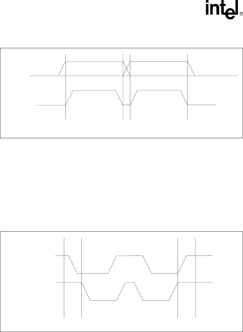
IXF1104 Quad-Port 10/100/1000 Mbps Ethernet Media Access Controller
112 Datasheet
Document Number: 278757
Revision Number: 007
Revision Date: March 25, 2004
5.7.3.6.1 Start Condition
A High-to-Low transition of I2C_DATA, with I2C_CLK High, is a start condition that must
precede any other command (see Figure 26).
5.7.3.6.2 Stop Condition
A Low-to-High transition of the I2C_DATA with I2C_CLK High is a stop condition. After a Read
sequence, the stop command places the E²PROM and the optical module in a standby power mode
(see Figure 26).
5.7.3.6.3 Acknowledge
All addresses and data words are serially transmitted to and from the optical module in 8-bit words.
The optical module E²PROM sends a zero to acknowledge that it has received each word, which
happens during the ninth clock cycle (see Figure 27).
Figure 25. Data Validity Timing
DATA STABLE DATA STABLE
DATA
CHANGE
I2C_Data
I2C_Clk
Figure 26. Start and Stop Definition Timing
START STOP
I2C_Data
I2C_Data
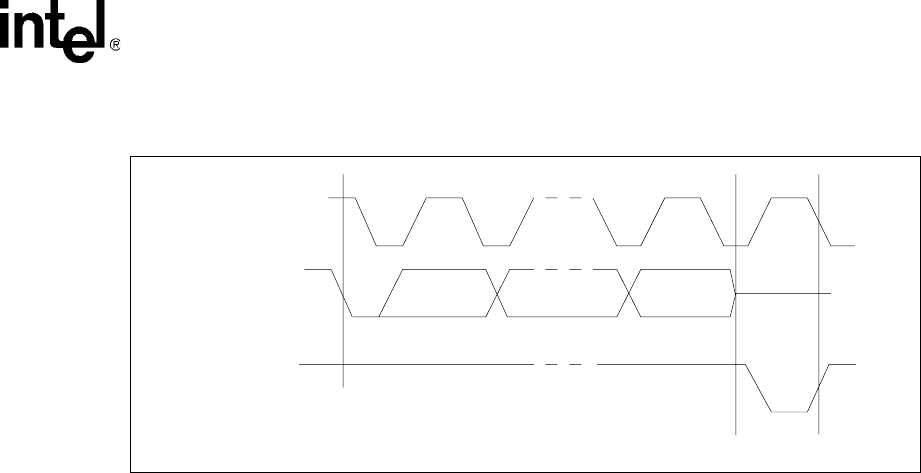
IXF1104 Quad-Port 10/100/1000 Mbps Ethernet Media Access Controller
Datasheet 113
Document Number: 278757
Revision Number: 007
Revision Date: March 25, 2004
5.7.3.6.4 Memory Reset
After an interruption in protocol, power loss, or system reset, any 2-wire optical module can be
reset by following three steps:
1. Clock up to 9 cycles
2. Wait for I2C_DATA High in each cycle while I2C_CLK is High
3. Initiate a start condition.
5.7.3.6.5 Device Addressing
All E²PROMs in SFP optical module devices require an 8-bit device address word following a start
condition to enable the chip to read or write. The device address word consists of a mandatory one,
zero sequence for the four most-significant bits. This is common to all devices. The next three bits
are the A2, A1, and A0 device address bits that are tied to zero in an optical module. The eighth bit
of the device address is the Read/Write operation select bit. A Read operation is initiated if this bit
is High and a Write operation is initiated if this bit is Low.
Upon comparison of the device address, the optical module outputs a zero. If a comparison is not
made, the optical module E²PROM returns to a standby state.
5.7.3.6.6 Random Read Operation
A random Read requires a “dummy” Byte/Write sequence to load the data word address. The
“dummy” write is achieved by first sending the device address word with the Read/Write bit
cleared to Low, which signals a Write operation. The optical module acknowledges receipt of the
device address word. The IXF1104 sends the data word address, which is again acknowledged by
the optical module. The IXF1104 generates another start condition. This completes the “dummy”
write and sets the optical module E²PROM pointers to the desired location.
The IXF1104 initiates a current address read by sending a device address with the Read/Write bit
set High. The optical module acknowledges the device address and serially clocks out the data
word. The IXF1104 does not respond with a zero but generates a stop condition (see Figure 28).
Figure 27. Acknowledge Timing
START ACKNOWLEDGE
I2C_Data
DATA IN
DATA OUT
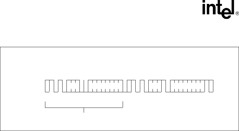
IXF1104 Quad-Port 10/100/1000 Mbps Ethernet Media Access Controller
114 Datasheet
Document Number: 278757
Revision Number: 007
Revision Date: March 25, 2004
5.8 LED Interface
The IXF1104 uses a Serial interface, consisting of three signals, to provide LED data to some form
of external driver. This provides the data for 12 separate direct drive LEDs and allows three LEDs
per MAC port.
There are two modes of operation, each with its own separate LED decode mapping. Modes of
operation and LEDs are detailed in the following sections.
5.8.1 Modes of Operation
There are two modes of operation: Mode 0 and Mode 1. Mode selection is accomplished by using
the LED_SEL_MODE bit. This bit is globally selected and controls the operation of all ports (see
Table 109 “LED Control ($0x509)” on page 189).
Mode 0: (LED_SEL_MODE = 0 [Default]): This mode selects operations compatible with the
SGS Thompson M5450 LED Display Driver device. This device converts the serial data stream,
output by the IXF1104, into 30 direct-drive LED outputs. Although the LED interface is capable of
driving all 30 LEDs, only twelve will be driven in the four-port IXF1104, three LEDs per port.
Mode 1: (LED_SEL_MODE = 1): This mode is used with standard TTL (74LS599) or HCMOS
(74HC599) octal shift registers with latches, providing the most general and cost-effective
implementation of the serial data stream conversion.
In addition to these physical modes of operation, there are two types of specific LED data decodes
available for fiber and copper modes. This option is a global selection and controls the operation of
all ports (see Table 109 “LED Control ($0x509)” on page 189).
5.8.2 LED Interface Signal Description
The IXF1104 LED interface consists of three output signal signals that are 2.5 V CMOS level pads.
Table 31 provides LED signal names, pin numbers, and descriptions.
Figure 28. Random Read
DEVICE
ADDRESS
DEVICE
ADDRESS
WORD
ADDRESS
I2
C_Data Line
DUMMY WRI TE
(* = DON' T CARE bi t for 1k)
START
S
T
A
R
T
R
E
A
D
S
T
A
R
T
W
R
I
T
E
S
T
O
P
M
S
B
M
S
B
M
S
B
L
S
B
R
/
W
L
S
B
DATAn
L
S
B
A
C
K
N
O
A
C
K
A
C
K
*
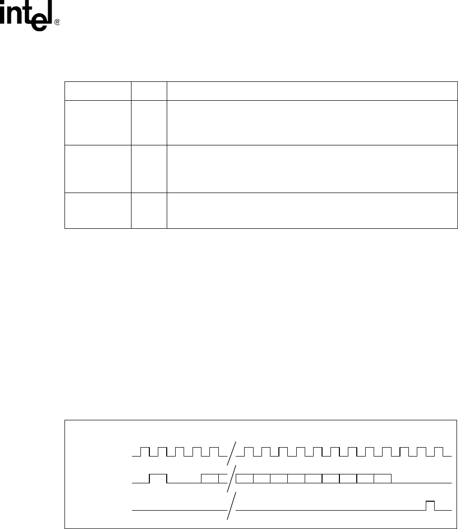
IXF1104 Quad-Port 10/100/1000 Mbps Ethernet Media Access Controller
Datasheet 115
Document Number: 278757
Revision Number: 007
Revision Date: March 25, 2004
5.8.3 Mode 0: Detailed Operation
Note: Please refer to the SGS Thompson* M5450 datasheet for device-operation information.
The operation of the LED Interface in Mode 0 is based on a 36-bit counter loop. The data for each
LED is placed in turn on the serial data line and clocked out by the LED_CLK. Figure 29 shows the
basic timing relationship and relative positioning in the data stream of each bit.
Figure 29 shows the 36 clocks that are output on the LED_CLK pin. The data is changed on the
falling edge of the clock and is valid for almost the entire clock cycle. This ensures that the data is
valid during the rising edge of the LED_CLK, which clocks the data into the M5450 device.
The actual data shown in Figure 29 consists of a chain of 36 bits, 12 of which are valid LED
DATA. The 36-bit data chain is built up as follows:
Table 31. LED Interface Signal Descriptions
Pin Name Pin # Pin Description
LED_CLK K24
This signal is an output that provides a continuous clock synchronous to the
serial data stream output on the LED_DATA pin. This clock has a maximum
speed of 720 Hz.
The behavior of this signal remains constant in all modes of operation.
LED_DATA M22
This signal provides the data, in various formats, as a serial bit stream. The data
must be valid on the rising edge of the LED_CLK signal.
In Mode 0, the data presented on this pin is TRUE (Logic 1 = High).
In Mode 1, the data presented on this pin is INVERTED (Logic 1 = Low).
LED_LATCH L22
This is an output pin, and the signal is used only in Mode 1 as the Latch enable
for the shift register chain.
This signal is not used in Mode 0, and should be left unconnected.
Figure 29. Mode 0 Timing
122 23 24 25 26 27 28 29 30
13534333231302928272625234
LED_CLK
LED_DATA
LED_LATCH

IXF1104 Quad-Port 10/100/1000 Mbps Ethernet Media Access Controller
116 Datasheet
Document Number: 278757
Revision Number: 007
Revision Date: March 25, 2004
When implemented on the board with the M5450 device, the LED DATA bit 1 appears on Output
bit 3 of the M5450 and the LED DATA bit 2 appears on Output bit 4, etc. This means that Output
bits 1, 2, and 15 through 35 will never have valid data and should not be used.
5.8.4 Mode 1: Detailed Operation
Note: Please refer to generic specifications for 74LS/HC599 for information on device operation.
The operation of the LED Interface in Mode 1 is based on a 36-bit counter loop. The data for each
LED is placed in turn on the serial data line and clocked out by the LED_CLK. Figure 30 on
page 117 shows the basic timing relationship and relative positioning in the data stream of each bit.
Figure 30 on page 117 shows the 36 clocks which are output on the LED_CLK pin. The data is
changed on the falling edge of the clock and is valid for the almost the entire clock cycle. This
ensures that the data is valid during the rising edge of the LED_CLK, which clocks the data into the
shift register chain devices.
The LED_LATCH signal is required in Mode 1, and latches the data shifted into the shift register
chain into the output latches of the 74HC599 device. Figure 30 shows that the LED_LATCH signal
is active High during the Low period on the 35th LED_CLK cycle. This avoids any possibility of
trying to latch data as it is shifting through the register.
When this operation mode is implemented on a board with a shift register chain containing three
74HC599 devices, the LED DATA bit 1 is output on Shift register bit 1, and so on up the chain.
Only Shift register bits 31 and 32 do not contain valid data.
The actual data shown in Figure 30 consists of a 36-bit chain, of which 12 bits are valid LED
DATA. The 36-bit data chain is built up as shown in Figure 30.
Table 32. Mode 0 Clock Cycle to Data Bit Relationship
LED_CLK Cycle LED_DATA
Name LED_DATA Description
1START BIT
This bit synchronizes the M5450 device to expect 35 bits of data to
follow.
2:3 PAD BITS These bits are used only as fillers in the data stream to extend the
length from the actual 12-bit LED DATA to the required 18-bit frame
length. These bits should always be a logic 0.
4:15 LED DATA 1-12
These bits are the actual data transmitted to the M5450 device. The
decode for each individual bit in each mode is defined in Table 34 on
page 118.
The data is TRUE. Logic 1 (LED ON) = High
36:38 PAD BITS These bits are used as fillers in the data stream to extend the length
from the actual 30-bit LED DATA to the required 36-bit frame length.
These bits should always be a logic 0.
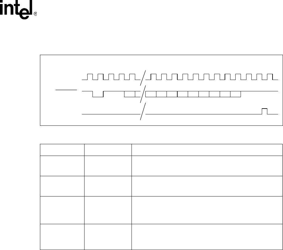
IXF1104 Quad-Port 10/100/1000 Mbps Ethernet Media Access Controller
Datasheet 117
Document Number: 278757
Revision Number: 007
Revision Date: March 25, 2004
Note: The LED_DATA signal is now inverted from the state in Mode 0.
5.8.5 Power-On, Reset, Initialization
The LED interface is disabled at power-on or reset. The system software controller must enable the
LED interface. The internal state machines and output signals are held in reset until the full
IXF1104 4-Port Gigabit Ethernet Media Access Controller device configuration is completed. This
is done by setting the LED_ENABLE bit to a logic 1 (see Table 109 “LED Control ($0x509)” on
page 189). The power-on default for this bit is logic 0.
5.8.6 LED DATA Decodes
The data transmitted on the LED_DATA line is determined by programming the global operation
mode as either fiber or copper. Table 34 shows the data decode of the data for both fiber and copper
MACs.
Figure 30. Mode 1 Timing
Table 33. Mode 1 Clock Cycle to Data Bit Relationship
LED_CLK Cycle LED_DATA Name LED_DATA Description
1START BITThis bit has no meaning in Mode 1 operation and is shifted out of
the 16-stage shift register chain before the LED_LATCH signal is
asserted.
2:3 PAD BITS These bits have no meaning in Mode 1 operation and are shifted
out of the 16-stage shift register chain before the LED_LATCH
signal is asserted.
4:15 LED DATA 1-12
These bits are the actual data to be transmitted to the 16-stage shift
register chain. The decode for each bit in each mode is defined in
Table 34 on page 118.
The data is INVERTD. Logic 1 (LED ON) = Low.
36:38 PAD BITS
These bits have no meaning in Mode 1 operation and are latched
into positions 31 and 32 in the shift register chain. These bits are
not considered as valid data and should be ignored. They should
always be a Logic 0 = High.
122 23 24 25 26 27 28 29 30
13534333231302928272625234
LED_CLK
LED_DATA
LED_LATCH

IXF1104 Quad-Port 10/100/1000 Mbps Ethernet Media Access Controller
118 Datasheet
Document Number: 278757
Revision Number: 007
Revision Date: March 25, 2004
Note: The data decode of the LED bits is independent of the Physical mode selection.
5.8.6.1 LED Signaling Behavior
Operation in each mode for the decoded LED data in Table 34 is detailed in Table 35 and Table 36.
5.8.6.1.1 Fiber LED Behavior
Table 34. LED_DATA# Decodes
LED_DATA# MAC Port # Fiber Designation Copper Designation
1
0
Rx LED—Amber Link LED—Amber
2 Rx LED—Green Link LED—Green
3 TX LED—Green Activity LED—Green
4
1
Rx LED—Amber Link LED—Amber
5 Rx LED—Green Link LED—Green
6 TX LED—Green Activity LED—Green
7
2
Rx LED—Amber Link LED—Amber
8 Rx LED—Green Link LED—Green
9 TX LED—Green Activity LED—Green
10
3
Rx LED—Amber Link LED—Amber
11 Rx LED—Green Link LED—Green
12 TX LED—Green Activity LED—Green
Table 35. LED Behavior (Fiber Mode)
Type Status Description
RXLED
Off Synchronization occurs but no packets are received
and the “Link LED Enable ($0x502)” is not set.
Amber On RX Synchronization has not occurred or no optical
signal exists.
Amber Blinking The port has remote fault and the “Link LED Enable
($0x502)” is not set (based on remote fault bit setting
received in Rx_Config word).
Green On RX Synchronization occurs and the “Link LED Enable
($0x502)” bit is set.
Green Blinking RX Synchronization occurs and the port is receiving
data.
TXLED
Off The port is not transmitting data or the “Link LED
Enable ($0x502)” is not set.
Green Blinking The port is transmitting data and the “Link LED Enable
($0x502)” bit is set
NOTE: Table 35 assumes the port is enabled in the “Port Enable ($0x500)” and the LEDs are enabled in the
“LED Control ($0x509)”. If a port is not enabled, all the LEDs for that port will be off. If the LEDs are not
enabled, all of the LEDs will be off.

IXF1104 Quad-Port 10/100/1000 Mbps Ethernet Media Access Controller
Datasheet 119
Document Number: 278757
Revision Number: 007
Revision Date: March 25, 2004
5.8.6.1.2 Copper LED Behavior
5.9 CPU Interface
The CPU interface block provides access to registers and statistics in the IXF1104. The interface is
asynchronous externally and operates within the 125 MHz clock domain internally. The interface
provides access to the following:
•Receive statistics registers
•Transmit statistics registers
•Receive FIFO registers
•Transmit FIFO registers
•Global configuration and control registers
•MAC_0 to MAC_3 registers
The CPU interface width can be configured with the two strap signals (UPX_WIDTH[1:0]) to
operate as an 8-bit, 16-bit, or 32-bit bus. All internal accesses to registers are 32-bit (4, 2, or 1 data
cycles respectively are required to fully access a register). When operating in 8-bit or 16-bit mode,
read data for bytes [3:1] is strobed into read holding registers when byte [0] is read. Subsequent
reads of bytes {1, 2, 3} in byte mode or of bytes {2,3} in 16-bit mode are supplied from the holding
register independent of the upper address bits. On write accesses in 8-bit mode, the data of bytes
{0, 1, 2} is similarly captured in internal write holding registers and the complete 32-bit write is
committed when byte[3] is written to the IXF1104. When writing in 16-bit mode, bytes [1:0] are
captured, and the double-word is committed when bytes [3:2] are written. The complete address for
write is ignored (except for the write which causes the commit operation).
Table 36. LED Behavior (Copper Mode)
Type Status Description
Link LED
Off Port does not have a remote fault and “LED Control
($0x509)” on page 189 bit is not set.
Amber On Port has an RGMII RXERR condition detected and
“LED Control ($0x509)” on page 189 bit is set
Amber Blinking Port has a remote fault and “LED Fault Disable
($0x50B)” on page 190 is not set.
Green On “LED Control ($0x509)” on page 189 bit is set and port
does not have an RGMII RXERR error or remote fault
condition present.
Activity LED - Green
Off Port is not transmitting and receiving data.
Blinking
“LED Control ($0x509)” on page 189 set: Port is
transmitting and/or receiving.
“LED Control ($0x509)” on page 189 not set: Port is
receiving data.
NOTE: Table 34 “LED_DATA# Decodes” assumes the port is enabled in the “Port Enable ($0x500)” on
page 187 and the LEDs are enabled in the “LED Control ($0x509)” on page 189. If a port is not
enabled, all the LEDs for that port are off. If the LEDs are not enabled, all of the LEDs are off.
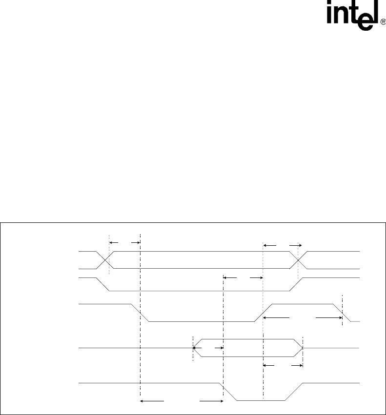
IXF1104 Quad-Port 10/100/1000 Mbps Ethernet Media Access Controller
120 Datasheet
Document Number: 278757
Revision Number: 007
Revision Date: March 25, 2004
5.9.1 Functional Description
5.9.1.1 Read Access
Read access involves the following:
•Detect assertion of asynchronous Read control signal and latch address
•Generate internal Read strobe
•Drive valid data onto processor bus
•Assert asynchronous Ready signal for required length of time
Figure 31 shows the timing of the asynchronous interface for Read access.
5.9.1.2 Write Access
Write process involves the following:
•Detect assertion of asynchronous Write control signal and latch address
•Detect de-assertion of asynchronous Write control signal and latch data
•Generate internal Write strobe
•Assert asynchronous Ready signal for required length of time
Figure 32 shows the timing of the asynchronous interface for Write accesses.
Figure 31. Read Timing Diagram - Asynchronous Interface
TCAS TCAH
TCRR
TCDRS
TCDRH
TCDRD
TCRH
uPx_ADD[12:0]
uPx_RdN
uPx_CsN
uPx_Data[31:0]
uPx_RdyN
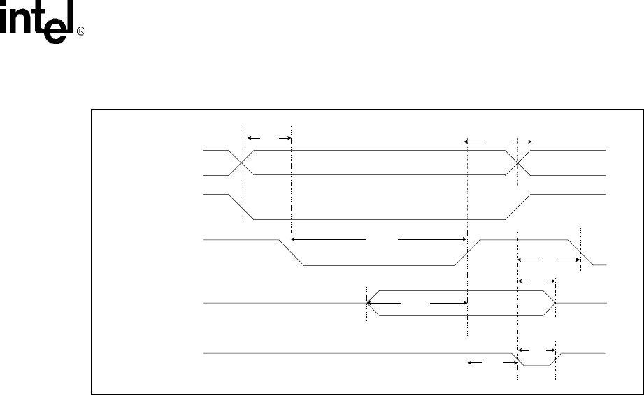
IXF1104 Quad-Port 10/100/1000 Mbps Ethernet Media Access Controller
Datasheet 121
Document Number: 278757
Revision Number: 007
Revision Date: March 25, 2004
5.9.1.3 CPU Timing Parameters
For information on the CPU interface Read and Write cycle AC timing parameters, refer to Figure
47 “CPU Interface Read Cycle AC Timing” on page 148, Figure 48 “CPU Interface Write Cycle
AC Timing” on page 148, and Table 54 “CPU Interface Write Cycle AC Signal Parameters” on
page 149.
5.9.2 Endian
The Endian of the CPU interface may be changed to allow connection of various CPUs to the
IXF1104 4-Port Gigabit Ethernet Media Access Controller. The Endian selection is determined by
setting the Endian bit in the “CPU Interface ($0x508)".
The following describes Endianness control:
•There is a byte swapper between the internal 32-bit bus and the external 32-bit bus.
•In 8-bit or 16-bit mode operation, the byte packer/byte unpacker holding registers sink and
source data just like the 32-bit external bus in 32-bit mode.
•The “CPU Interface ($0x508)" selects Big-Endian or Little-Endian mode.
•The byte swapper causes the behavior seen in Table 37 for accessing a register with data bits
data[31:0].
Figure 32. Write Timing Diagram - Asynchronous Interface
TCAS TCAH
TCWL
TCDWS
TCDWD
TCYD
TCWH
uPx_Add[12:0]
uPx_WrN
uPx_CsN
uPx_Data[31:0]
uPx_RdyN
TCDWH

IXF1104 Quad-Port 10/100/1000 Mbps Ethernet Media Access Controller
122 Datasheet
Document Number: 278757
Revision Number: 007
Revision Date: March 25, 2004
5.10 TAP Interface (JTAG)
The IXF1104 includes an IEEE 1149.1 compliant Test Access Port (TAP) interface used during
boundary scan testing. The interface consists of the following five signals:
•TDI – Serial Data Input
•TMS – Test Mode Select
•TCLK – TAP Clock
•TRST_L – Active Low asynchronous reset for the TAP
•TDO – Serial Data Output
TDI and TMS require external pull-up resistors to float the signals High per the IEEE 1149.1
specification. Pull-ups are recommended on TCK and TDO. For normal operation, TRST_L can be
pulled Low, permanently disabling the JTAG interface. If the JTAG interface is used, the TAP
controller must be reset as described in Section 5.10.1, “TAP State Machine” on page 122 and
returned to a logic High.
5.10.1 TAP State Machine
The TAP signals drive a TAP controller, which implements the 16-state state machine specified by
the IEEE 1149.1 specification. Following power-up, the TAP controller must be reset by one of
following two mechanisms:
•Asynchronous reset
•Synchronous reset
Asynchronous reset is achieved by pulsing or holding TRST_L Low. Synchronous reset is
achieved by clocking TCLK with five clock pulses while TMS is held or floats High. This ensures
that the boundary scan cells do not block the pin to core connections in the IXF1104.
Table 37. Byte Swapper Behavior
UPX_BADD
[1:0]
Little Endian Big Endian
32-bit 16-bit 8-bit132-bit 16-bit 8-bit1
UPX_DATA_
[31:0] UPX_DATA_
[15:0] UPX_DATA
[7:0] UPX_DATA
[31:0] UPX_DATA
[15:0] UPX_DATA
[7:0]
00 [31:0] [15:0] [7:0]
[7:0]
[15:8]
[23:16
[31:24]
[7:0]
[15:8] [7:0]
01 – – [15:8] – – [15:8]
10 – [31:16] [23:16] – [23:16]
[31:24] [23:16]
11 – – [31:24] – – [31:24]
1. In 8-bit mode, data is output in Little Endian format regardless of the IXF1104 Endian setting.

IXF1104 Quad-Port 10/100/1000 Mbps Ethernet Media Access Controller
Datasheet 123
Document Number: 278757
Revision Number: 007
Revision Date: March 25, 2004
5.10.2 Instruction Register and Supported Instructions
The instruction register is a 4-bit register that enacts the boundary scan instructions. After the state
machine resets, the default instruction is IDCODE. The decode logic in the TAP controller selects
the appropriate data register and configures the boundary scan cells for the current instruction.
Table 38 shows the supported boundary-scan instructions.
Table 38. Instruction Register Description
Instruction Code Description Data Register
BYPASS 1111 1-bit Bypass Bypass
EXTEST 0000 External Test Boundary Scan
SAMPLE 0001 Sample Boundary Boundary Scan
IDCODE 0110 ID Code Inspection ID
HIGHZ 0101 Float Boundary Bypass
CLAMP 0111 Clamp Boundary Bypass

IXF1104 Quad-Port 10/100/1000 Mbps Ethernet Media Access Controller
124 Datasheet
Document Number: 278757
Revision Number: 007
Revision Date: March 25, 2004
5.10.3 ID Register
The ID register is a 32-bit register. The IDCODE instruction connects this register between TDI
and TDO. See Table 112 “JTAG ID ($0x50C)” on page 191 for detailed information.
5.10.4 Boundary Scan Register
The Boundary Scan register is a shift register made up of all the boundary scan cells associated
with the device signals. The number, type, and order of the boundary scan cells are specified in the
IXF1104 BSDL file. The EXTEST and SAMPLE instructions connect this register between TDI
and TDO.
5.10.5 Bypass Register
The Bypass register is a 1-bit register that bypasses the IXF1104 to reduce the JTAG chain length
when accessing other devices on the chain besides the IXF1104. The BYPASS, HIGHZ, and
CLAMP instructions connect this register between TDI and TDO.
5.11 Loopback Modes
The IXF1104 provides two loopback modes for device diagnostic testing when it has been
integrated into a user system. A line-side loopback allows the line-side receive interface to be
looped back to the transmit line-side interface. A SPI3 loopback mode allows the SPI3 transmit
interface to be looped back to the SPI3 receive interface.
5.11.1 SPI3 Interface Loopback
To provide a diagnostic loopback feature on the SPI3 interface, it is possible to configure the
IXF1104 to loop back any data written to the IXF1104 through the SPI3 transmit interface back to
the SPI3 receive interface. This is accomplished using the data path shown in Figure 33.
Note: Loopback packets also appear on the line side TX interface.
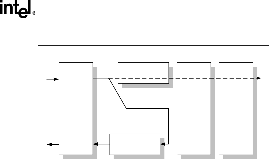
IXF1104 Quad-Port 10/100/1000 Mbps Ethernet Media Access Controller
Datasheet 125
Document Number: 278757
Revision Number: 007
Revision Date: March 25, 2004
Note: There is a restriction when using this loopback mode. At least one clock cycle is required between
a TEOP assertion and a TSOP assertion. This is required when the pre-pend feature of the receive
FIFO is enabled to allow the addition of the extra two bytes to the data sent on the transmit
interface. Where the pre-pend feature has not been enabled, data can be sent back-to-back on the
transmit SPI3 interface with TSOP following TEOP on the next cycle.
To configure the IXF1104 to use the SPI3 loopback mode, the “RX FIFO SPI3 Loopback Enable
for Ports 0 - 3 ($0x5B2)" must be configured. Each IXF1104 port has a unique bit in this register
designated to control loopback. It is possible to have individual ports in a loopback mode while
other ports continue to operate in a normal mode.
5.11.2 Line Side Interface Loopback
To provide a diagnostic loopback feature on the line-side interfaces, the IXF1104 can be configured
to loop back any data received by the IXF1104 through one of the line interfaces back to the
corresponding transmit line interface. This is done by using the data path shown in Figure 34. The
line-side interface can be either SerDes, RGMII or GMII. Please note that it is not possible to loop
one line-side interface back to a different one (for example, Rx SerDes looped back to transmit
RGMII).
Figure 33. SPI3 Interface Loopback Path
SPI3 Interface
Block
TX
RX
Line Side
Interface
MAC
TX FIFO
RX FIFO
B3229-01
SPI3 Internal Loopback
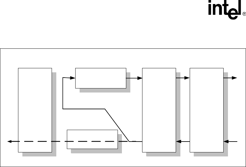
IXF1104 Quad-Port 10/100/1000 Mbps Ethernet Media Access Controller
126 Datasheet
Document Number: 278757
Revision Number: 007
Revision Date: March 25, 2004
When the IXF1104 is configured in this loopback mode, all of the MAC functions and features are
available, including flow control and pause-packet generation.
To configure the IXF1104 to use the line-side loopback mode, the “Loop RX Data to TX FIFO
(Line-Side Loopback) Ports 0 - 3 ($0x61F)" must be configured. Each IXF1104 port has a unique
bit in this register designated to control the loopback. It is possible to have individual ports in a
loopback mode while other ports continue to operate in a normal mode.
Note: Line side interface loopback packets also appear at the SPI3 interface.
5.12 Clocks
The IXF1104 system interface has several reference clocks, including the following:
•SPI3 data path input clocks
•RGMII input and output clocks
•MDIO output clock
•JTAG input clock
•I2C clock
•LED output clock.
This section details the unique clock source requirements.
5.12.1 System Interface Reference Clocks
The following system interface clock is required by the IXF1104:
•CLK125
Figure 34. Line Side Interface Loopback Path
RX FIFO
SPI3 Interface
Block
TX
RX
Line Side
Interface
MAC
TX FIFO
B3230-01
Line Side Internal Loopback

IXF1104 Quad-Port 10/100/1000 Mbps Ethernet Media Access Controller
Datasheet 127
Document Number: 278757
Revision Number: 007
Revision Date: March 25, 2004
5.12.1.1 CLK125
The system interface clock, which supplies the clock to the majority of the internal circuitry, is the
125 MHz clock. The source of this clock must meet the following specifications:
•2.5 V CMOS drive
•+/- 50 ppm
•Maximum duty cycle distortion 40/60
5.12.2 SPI3 Receive and Transmit Clocks
The IXF1104 transmit clock requirements include the following:
•3.3 V LVTTL drive
•+/- 50 ppm
•Maximum frequency of 133 MHz in MPHY mode
•Maximum frequency of 125 MHz in SPHY mode
•Maximum duty cycle distortion 45/55
The IXF1104 meets the following specifications for the receive clock:
•3.3 V LVTTL drive
•+/- 50 ppm
•Maximum frequency of 133 MHz in MPHY mode
•Maximum frequency of 125 MHz in SPHY mode
•Maximum duty cycle distortion 45/55
5.12.3 RGMII Clocks
The RGMII interface is governed by the Hewlett-Packard* 1.2a specification. The IXF1104
compliant to this specification with the following:
•2.5 V CMOS drive
•Maximum duty cycle distortion 40/60
•+/- 100 ppm
•125 MHz for 1000 Mbps, 25 MHz for 100 Mbps and 2.5 MHz for 10 Mbps
5.12.4 MDC Clock
The IXF1104 supports the IEEE 802.3 MII Management Interface, also known as the Management
Data Input/Output (MDIO) Interface. The IXF1104 meets the following specifications for this
clock:
•2.5 V CMOS drive
•2.5/18 MHz operation (selectable by the MDC speed bit in the “MDIO Control ($0x683)")
•50/50 duty cycle for 2.5 MHz operation

IXF1104 Quad-Port 10/100/1000 Mbps Ethernet Media Access Controller
128 Datasheet
Document Number: 278757
Revision Number: 007
Revision Date: March 25, 2004
•43/57 duty cycle for 18 MHz operation
5.12.5 JTAG Clock
The IXF1104 supports JTAG. The source of this clock must meet the following specifications:
•3.3 V CMOS drive
•Maximum clock frequency 11 MHz
•Maximum duty cycle distortion 40/60
5.12.6 I2C Clock
The IXF1104 supports a single-output I2C clock to support all ten Optical Module interfaces. The
IXF1104 meets the following specifications for this clock:
•2.5 V CMOS drive
•Maximum clock frequency of 100 KHz
5.12.7 LED Clock
The IXF1104 supports a serial LED data stream and meets the following specifications for this
clock:
•2.5 V CMOS drive
•Maximum frequency of 720 Hz
•Maximum duty cycle distortion 50/50

IXF1104 4-Port Gigabit Ethernet Media Access Controller
Datasheet 129
Document Number: 278757
Revision Number: 007
Revision Date: March 25, 2004
6.0 Applications
6.1 Change Port Mode Initialization Sequence
Use the change port mode initialization sequence after power-up and anytime a port is configured
into or switching between fiber or copper mode, switching to/from RGMII and GMII modes, or
switching speeds and duplex in RGMII mode.
The following sequence applies to all four ports and can be done simultaneously for all ports or as
a subset of the ports.
1. Place the MAC in reset for the port(s) which require a change by asserting (set to 1) the “MAC
Soft Reset ($0x505)”.
2. Place the TX FIFO in reset for the port(s) which require a change by asserting (set to 1) the
“TX FIFO Port Reset ($0x620)”.
3. Disable the port(s) which require change by de-asserting (set to 0) the appropriate bits in the
“Port Enable ($0x500)”.
4. Wait 1 µs.
5. De-assert (set to 0) “Clock and Interface Mode Change Enable Ports 0 - 3 ($0x794)” for the
ports being changed.
6. Set the speed, mode, and duplex as follows for the ports being changed:
a. Copper mode:
Select copper mode for the “Interface Mode ($0x501)” ports.
Set the per-port “MAC IF Mode and RGMII Speed ($ Port_Index + 0x10)” to the
appropriate speed and RGMII/GMII interface setting.
Set the per-port “Desired Duplex ($ Port_Index + 0x02)”.
Note: Half-duplex is supported only when RGMII 10 Mbps or 100 Mbps is selected in the
“MAC IF Mode and RGMII Speed ($ Port_Index + 0x10)”.
b. Fiber mode:
Select fiber mode by setting the appropriate bit to 0 in the “Interface Mode ($0x501)”
ports.
7. Assert (set to 1) “Clock and Interface Mode Change Enable Ports 0 - 3 ($0x794)” for the ports
being changed.
8. Wait 1 µs.
9. De-assert (set to 0) “MAC Soft Reset ($0x505)” for the ports being changed.
10. De-assert (set to 0) “TX FIFO Port Reset ($0x620)” for the ports being changed.
11. Wait 1 to 2 µs.
12. Set the “Diverse Config Write ($ Port_Index + 0x18)” to the appropriate value as follows:
a. Copper mode:
Write the reserved bits to the default value.

IXF1104 4-Port Gigabit Ethernet Media Access Controller
130 Datasheet
Document Number: 278757
Revision Number: 007
Revision Date: March 25, 2004
Enable packet padding and CRC appending on transmitted packets in bits 6 and 7, as
needed.
Set bit 5 to 0x0.
b. Fiber Mode:
Write the reserved bits to the default value.
Enable Packet padding and CRC Appending on transmitted packets in bits 6 and 7, as
needed.
Set bit 5 to 1 to enable auto-negotiation.
Set bit 5 to 0 to enable forced mode operation.
13. Assert (set to 1) “Port Enable ($0x500)”.
14. Wait 1 to 2 µs.
15. Perform additional device configurations, as needed.

IXF1104 4-Port Gigabit Ethernet Media Access Controller
Datasheet 131
Document Number: 278757
Revision Number: 007
Revision Date: March 25, 2004
7.0 Electrical Specifications
Table 39 through Table 58 “LED Interface AC Timing Parameters” on page 153 and Figure 35
“SPI3 Receive Interface Timing” on page 136 through Figure 52 “LED AC Interface Timing” on
page 153 represent the target specifications of the following IXF1104 interfaces:
— SPI3
—JTAG
—MDIO
— Pause Control
—CPU
—LED
—System
— GMII and RGMII
—SerDes
— Optical Module
These specifications are not guaranteed and are subject to change without notice. Minimum and
maximum values listed in Table 41 “Intel® IXF1104 MAC DC Specifications” on page 133
through Table 58 “LED Interface AC Timing Parameters” on page 153 apply over the
recommended operating conditions specified in Table 40.
Table 39. Absolute Maximum Ratings
Parameter Symbol Min Max Units Comments
Supply voltage
VDD -0.3 2.2 volts Core digital power
VDD2, VDD3 -0.3 4.25 volts I/O digital power
VDD4, VDD5 -0.3 4.25 volts I/O digital power
AVDD1P8_1/2 -0.3 2.2 volts Analog power
AVDD2P5_1/2 -0.3 4.25 volts Analog power
Operating
temperature
Ambient TOPA -40 +85 °C Copper mode
Ambient TOPA 0.0 +70 °C Fiber mode
Storage temperature TST -40 +150 °C –
Caution: Exceeding these values may cause permanent damage to the device. Functional
operation under these conditions is not implied. Exposure to maximum rating
conditions for extended periods may affect device reliability.

IXF1104 4-Port Gigabit Ethernet Media Access Controller
132 Datasheet
Document Number: 278757
Revision Number: 007
Revision Date: March 25, 2004
7.1 DC Specifications
The IXF1104 supports the following I/O buffer types:
•2.5 V CMOS
•3.3 V LVTTL
•SerDes
Table 40. Recommended Operating Conditions
Parameter Symbol Min Typ Max Units
Recommended supply voltage
VDD 1.65 – 1.95 Volts
VDD2, VDD3 3.0 – 3.6 Volts
VDD4, VDD5 2.3 – 2.7 Volts
AVDD1P8_1
AVDD1P8_2 1.65 – 1.95 Volts
AVDD2P5_1
AVDD2P5_2 2.3 – 2.7 Volts
Operating Current
SerDes Operation
Transmitting and
receiving in
1000 Mbps mode
VDD
AVDD1P8_1
AVDD1P8_2 –0.780–Amps
VDD4
VDD5
AVDD2P5_1
AVDD2P5_2
–0.050–Amps
VDD2, VDD3 – 0.246 – Amps
Operating Current
RGMII Operation
Transmitting and
receiving in
1000 Mbps mode
VDD
AVDD1P8_1
AVDD1P8_2 –0.757–Amps
VDD4
VDD5
AVDD2P5_1
AVDD2P5_2
–0.224–Amps
VDD2, VDD3 – 0.208 0.235 Amps
Recommended
operating
temperature
Ambient TOPA 0 – 70 °C
Case with heat
sink TOPC-HS 0 – 122 °C
Case without heat
sink TOPC-NHS 0 – 121 °C
Power
consumption
SerDes Operation
Transmitting and
receiving in
1000 Mbps mode
– – 2.23 2.72 Watts
RGMII Operation
Transmitting and
receiving in
1000 Mbps mode
– – 2.84 3.4 Watts

IXF1104 4-Port Gigabit Ethernet Media Access Controller
Datasheet 133
Document Number: 278757
Revision Number: 007
Revision Date: March 25, 2004
See Section 5.1.7, “Packet Buffer Dimensions” on page 79 for additional information regarding I/O
buffer types. The related driver characteristics are described in this section.
Caution: IXF1104 input signals are not 5 V tolerant. Devices driving the IXF1104 must provide 3.3 V signal
levels or use level-shifting buffers to provide 3.3 V compatible levels. Otherwise, damage to the
IXF1104 will occur.
Table 41. Intel® IXF1104 MAC DC Specifications
Parameter Symbol Min Typ Max Units Comments
2.5 V CMOS I/O Cells
Input High voltage VIH 1.7 – – V 2.5 V I/Os
Input low voltage VIL – – 0.7 V 2.5 V I/Os
Output High voltage VOH 2.0 – – V 2.5 V I/Os
Output low voltage VOL – – 0.4 V 2.5 V I/Os
3.3 V I/O Cells
Input High voltage VIH 1.7 – – V 3.3 V LVTTL I/Os
Input low voltage VIL – – 0.7 V 3.3 V LVTTL I/Os
Output High voltage VOH 2.4 – – V 3.3 V LVTTL I/Os
Output low voltage VOL – – 0.4 V 3.3 V LVTTL I/Os
Table 42. SerDes Transmit Characteristics (Sheet 1 of 2)
Parameter Symbol
Normalized
Power
Drive
Settings1
Min Typ Max Units Comments
Transmit differential
signal level TxDfPP
0.50 180 230 325
mVpp diff AVDD1P8_2 terminated
to 1.8V; Rload = 50 Ω
1.00 350 440 700
1.33 425 580 900
2.00 600 770 1050
Transmit common
mode voltage range TxCMV
0.50 1300 1600 1940
mV AVDD1P8_2 terminated
to 1.8V; RLoad = 50
ohms; FIR coeffs = 0
1.00 1000 1400 1870
1.33 800 1300 1825
2.00 700 1100 1760
Differential signal rise/
fall time Diff rise/
fall 1.00 60 96 132 ps Rload = 50 Ω; 20% to
80% max
Differential output
impedance TxDiffZ – 60 105 150 Ω diff Nominal value = 100 Ω
differential
Receiver differential
voltage requirement at
center of receive eye RxDiffV – 200 – – mVp-p
diff –
1. Refer to Section 5.6.2.2, “Transmitter Programmable Driver-Power Levels” on page 103.

IXF1104 4-Port Gigabit Ethernet Media Access Controller
134 Datasheet
Document Number: 278757
Revision Number: 007
Revision Date: March 25, 2004
7.1.1 Undershoot / Overshoot Specifications
The overshoot figures given in this section represent the maximum voltage that can be applied
without affecting the reliability of the device (see Table 44).
Caution: If these limits are exceeded, damage to the device will occur.
7.1.2 RGMII Electrical Characteristics
The RGMII signals (including MDIO/MDC) are based on 2.5V CMOS interface voltages, as
defined by JEDEC EIA/JESD8-5 (see Table 45).
Receiver common
mode voltage range RxCMV – 900 1275 1650 mV –
Receiver termination
impedance RxZ – 40 51 62.5 Ω–
Signal detect level RxSigDet – 50 125 200 mVp-pdiff –
Table 43. Intel® IXF1104 MAC SerDes Receive Characteristics
Parameter Symbol
Normalized
Power
Drive
Settings
Min Typ Max Units Comments
Receiver differential
voltage requirement at
center of receive eye RxDiffV – 200 – – mVp-p diff –
Receiver common
mode voltage range RxCMV – 900 1275 1650 mV –
Receiver termination
impedance RxZ – 40 51 62.5 Ω–
Signal detect level RxSigDet – 50 125 200 mVp-pdiff –
Table 42. SerDes Transmit Characteristics (Sheet 2 of 2)
Parameter Symbol
Normalized
Power
Drive
Settings1
Min Typ Max Units Comments
1. Refer to Section 5.6.2.2, “Transmitter Programmable Driver-Power Levels” on page 103.
Table 44. Undershoot / Overshoot Limits
Pin Type Undershoot Overshoot
2.5 V CMOS -0.60 V 3.9 V
3.3 V LVTTL -0.60 V 3.9 V

IXF1104 4-Port Gigabit Ethernet Media Access Controller
Datasheet 135
Document Number: 278757
Revision Number: 007
Revision Date: March 25, 2004
Table 45. RGMII Power
Symbol Parameter Conditions Min Max Units
VOH Output High Voltage IOH = -1.0 MA; VCC = MIN 2.0 VDD +.3 V
VOL Output Low Voltage IOL = 1.0 MA; VCC = MIN GND -.3 0.40 V
VIH Input High Voltage VIH > VIH_MIN; VCC = MIN ––V
VIL Input Low Voltage VIL < VIL_MAX; VCC = MIN –.70V
IIH Input High Current VCC = MAX; VIN = 2.5V – 15 µA
IIL Input Low Current VCC = MAX; VIN = 0.4V -15 – µA
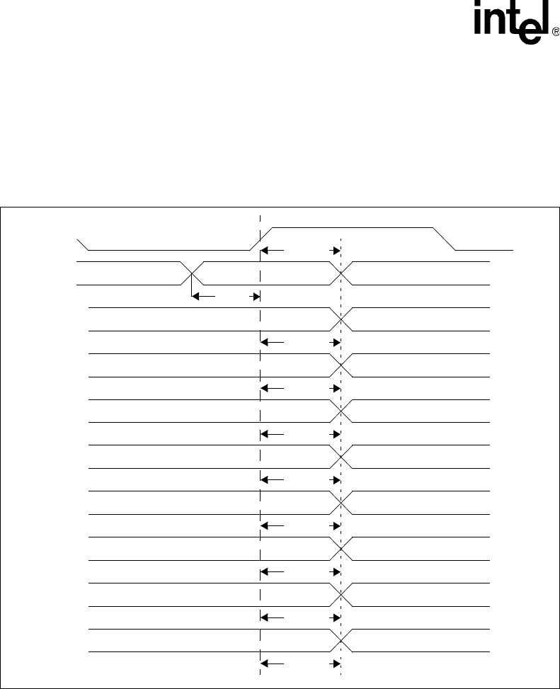
IXF1104 4-Port Gigabit Ethernet Media Access Controller
136 Datasheet
Document Number: 278757
Revision Number: 007
Revision Date: March 25, 2004
7.2 SPI3 AC Timing Specifications
7.2.1 Receive Interface Timing
Figure 35 and Table 46 illustrate and provide SPI3 receive interface timing information.
Figure 35. SPI3 Receive Interface Timing
RFCLK
RENB
RDAT[31:0]
RPRY
RMOD
RSOP
REOP
RERR
RVAL
RSX
THrenb
TSrenb
TPrdat
TPrprty
TPrmod
TPrsop
TPreop
TPrerr
TPrval
TPrsx

IXF1104 4-Port Gigabit Ethernet Media Access Controller
Datasheet 137
Document Number: 278757
Revision Number: 007
Revision Date: March 25, 2004
Table 46. SPI3 Receive Interface Signal Parameters
Symbol Parameter Min Max Units
– RFCLK frequency – 133 MHz
– RFCLK duty cycle 40 60 %
Tsrenb RENB setup time to RFCLK 1.8 – ns
Threnb RENB hold time to RFCLK 0.5 – ns
TPrdat RFCLK High to RDAT valid 1.5 3.7 ns
TPrprty RFCLK High to RPRTY valid 1.5 3.7 ns
TPrsop RFCLK High to RSOP valid 1.5 3.7 ns
TPreop RFCLK High to REOP valid 1.5 3.7 ns
TPrmod RFCLK High to RMOD valid 1.5 3.7 ns
TPrerr RFCLK High to RERR valid 1.5 3.7 ns
TPrval RFCLK High to RVAL valid 1.5 3.7 ns
TPrsx RFCLK High to RSX valid 1.5 3.7 ns
NOTES: Receive I/O Timing
1. When a setup time is specified between an input and a clock, the setup time is the time in nanoseconds
from the 1.4-volt point of the input to the 1.4-volt point of the clock.
2. When a hold time is specified between an input and a clock, the hold time is the time in nanoseconds from
the 1.4-volt point of the clock to the 1.4-volt point of the input.
3. Output propagation time is the time in nanoseconds from the 1.4-volt point of the reference signal to the
1.4-volt point of the output.
4. Maximum propagation delays are measured with a 30 pF load when operating OIF-SPI3 standard 104
MHz. Over-clocked rates of 125 MHz or higher are measured using a load of 20 pF.
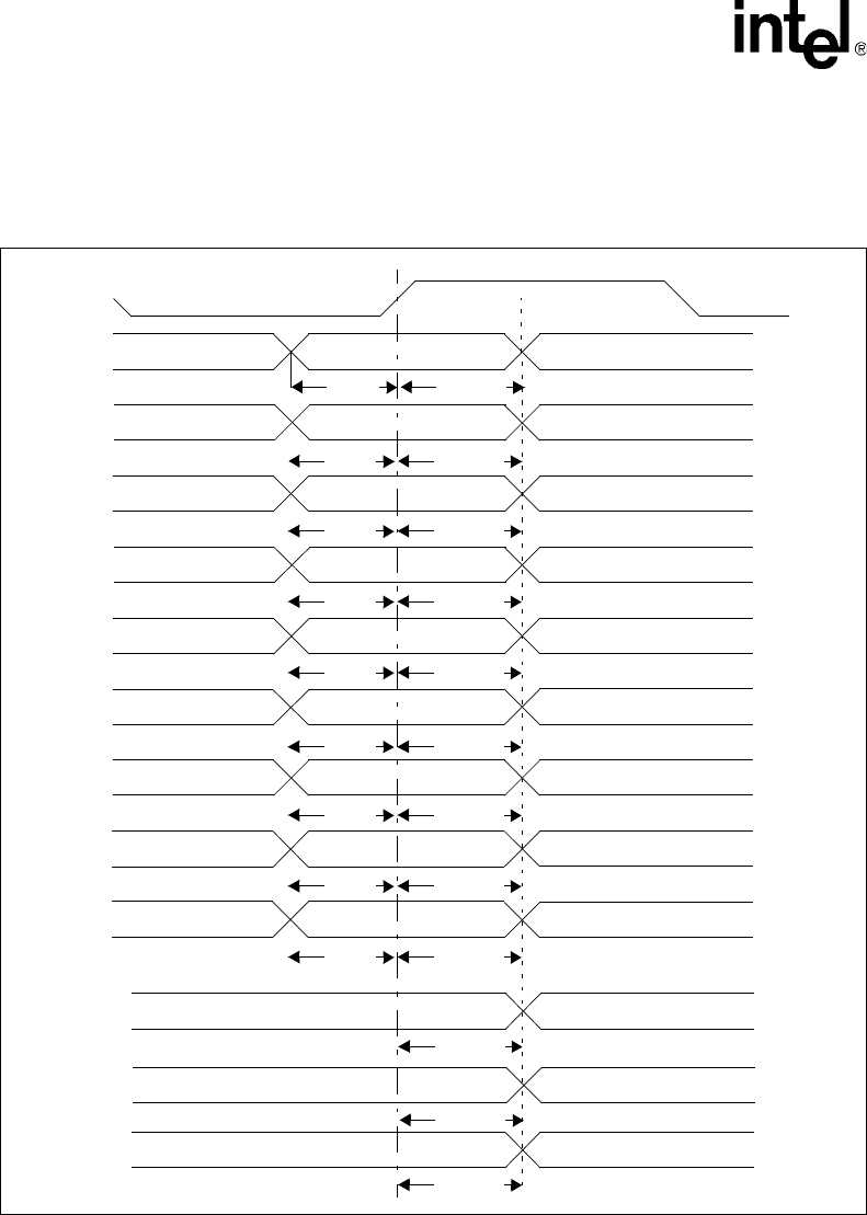
IXF1104 4-Port Gigabit Ethernet Media Access Controller
138 Datasheet
Document Number: 278757
Revision Number: 007
Revision Date: March 25, 2004
7.2.2 Transmit Interface Timing
Figure 36 and Table 47 illustrate and provide SPI3 transmit interface timing information.
Figure 36. SPI3 Transmit Interface Timing
TFCLK
TENB
TDAT[31:0]
TPRTY
TMOD[1:0]
TSOP
TEOP
TERR
TADR
TSX
THtenbTStenb
THtdatTStdat
THtprtyTStrpty
THtmodTStmod
THtsopTStsop
THteopTSteop
THterrTSterr
THtadrTStadr
THtsxTStsx
DTPA
TPdtpa
STPA
TPstpa
PTPA
TPptpa

IXF1104 4-Port Gigabit Ethernet Media Access Controller
Datasheet 139
Document Number: 278757
Revision Number: 007
Revision Date: March 25, 2004
Table 47. SPI3 Transmit Interface Signal Parameters
Symbol Parameter Min Max Units
– TFCLK frequency – 133 MHz
– TFCLK duty cycle 40 60 %
TStenb TENB setup time to TFCLK 1.8 – ns
THtenb TENB hold time to TFCLK 0.5 – ns
TStdat TDAT[31:0] setup time to TFCLK 1.8 – ns
THtdat TDAT[31:0} hold time to TFCLK 0.5 – ns
TStprty TRPTY setup time to TFCLK 1.8 – ns
THtprty TPRTY hold time to TFCLK 0.5 – ns
TStsop TSOP setup time to TFCLK 1.8 – ns
THtsop TSOP hold time to TFCLK 0.5 – ns
TSteop TEOP setup time to TFCLK 1.8 – ns
THteop TEOP hold time to TFCLK 0.5 – ns
TStmod TMOD setup time to TFCLK 1.8 – ns
THtmod TMOD hold time to TFCLK 0.5 – ns
TSterr TERR setup time to TFCLK 1.8 – ns
THterr TERR hold time to TFCLK 0.5 – ns
TStsx TSX setup time to TFCLK 1.8 – ns
THtsx TSX hold time to TFCLK 0.5 – ns
TStadr TADR setup time to TFCLK 1.8 – ns
THtadr TADR hold time to TFCLK 0.5 – ns
TPdtpa TFCLK High to DTPA valid 1.5 3.7 ns
TPstpa TFCLK High to STPA valid 1.5 3.7 ns
TPptpa TFCLK High to PTPA valid 1.5 3.7 ns
NOTES:Transmit I/O Timing:
1. When a setup time is specified between an input and a clock, the setup time is the time in nanoseconds
from the 1.4 V point of the input to the 1.4-volt point of the clock.
2. When a hold time is specified between an input and clock, the hold time is the time in nanoseconds from
the 1.4 V point of the clock to the 1.4-volt point of the input.
3. Output propagation delay time is the time in nanoseconds from the 1.4 V point of the reference signal to the
1.4 V point of the output.
IXF1104 4-Port Gigabit Ethernet Media Access Controller
140 Datasheet
Document Number: 278757
Revision Number: 007
Revision Date: March 25, 2004
7.3 RGMII AC Timing Specification
Figure 37 and Table 48 provide RGMII interface timing parameters.
Figure 37. RGMII Interface Timing
Table 48. RGMII Interface Timing Parameters
Symbol Parameter Min Typ Max Unit
TskewT Data-to-Clock Output Skew (at Transmitter) -500 0 500 ps
TskewR Data-to-Clock Input Skew (at Receiver)11–2.8ns
Tcyc Clock Cycle Duration27.2 8 8.8 ns
Duty_T Duty Cycle for Gigabit245 50 55 %
Duty_G Duty Cycle for 10/100T340 50 60 %
Tr/Tf Rise/Fall Time (20–80%) – – .75 ns
1. This implies that PC board design requires clocks to be routed so that an additional trace delay of greater
than 1.5 ns is added to the associated clock signal.
2. For 10 Mbps and 100 Mbps Tcyc scales to 400 ns +/– 40 ns and 40 ns +/– 4 ns respectively.
3. Duty cycle may be stretched/shrunk during speed changes or while transitioning to a received packet’s
clock domain, as long as minimum duty cycle is not violated and stretching occurs for no more than three
Tcyc of the lowest speed transitioned between.
B3251-01
TSkewT
TXC
(at Transmitter)
TXC
(at Receiver)
TD[3:0]
TX_CTL[n]
TSkewR
TD[3:0] TD[7:4]
TXEN TXERR
TSkewT
RXC
(at Transmitter)
RXC
(at Receiver)
RD[3:0]
RX_CTL
TSkewR
RD[3:0] RD[7:4]
RXDV RXERR
IXF1104 4-Port Gigabit Ethernet Media Access Controller
Datasheet 141
Document Number: 278757
Revision Number: 007
Revision Date: March 25, 2004
7.4 GMII AC Timing Specification
7.4.1 1000 Base-T Operation
Figure 38 and Figure 39 and Table 49 and Table 50 provide GMII AC timing specifications.
7.4.1.1 1000 BASE-T Transmit Interface
Figure 38. 1000BASE-T Transmit Interface Timing
Table 49. GMII 1000BASE-T Transmit Signal Parameters
Symbol Parameter Min Typ1Max Unit2
t1 TXD[7:0], TXEN, TXER Set-up to TXC High 2.5 – – ns
t2 TXD[7:0], TXEN, TXER Hold from TXC High 0.5 – – ns
t3 TXEN sampled to CRS asserted – – 16 BT
t4 TXEN sampled to CRS de-asserted – – 16 BT
1. Typical values are at 25oC and are for design aid only; not guaranteed and not subject to production
testing.
2. Bit Time (BT) is the duration of one bit as transferred to/from the PHY and is the reciprocal of bit rate. BT for
1000BASE-T = 10-9 or 1 ns.
B0634-01
GTX_CLK
TXEn
TXD[7:0]
TXER
CPS
t1
t3
t4
t2
IXF1104 4-Port Gigabit Ethernet Media Access Controller
142 Datasheet
Document Number: 278757
Revision Number: 007
Revision Date: March 25, 2004
7.4.1.2 1000BASE-T Receive Interface
Figure 39. 1000BASE-T Receive Interface Timing
Table 50. GMII 1000BASE-T Receive Signal Parameters
Symbol Parameter Min Typ1Max Unit2
t1 RXD[7:0], RX_DV, RXER Setup to Rx_CLK High 2.0 – – ns
t2 RXD[7:0], RX_DV, RXER Hold after Rx_CLK High 0.0 – – ns
1. Typical values are at 25oC and are for design aid only; not guaranteed and not subject to production
testing.
2. Bit Time (BT) is the duration of one bit as transferred to/from the PHY and is the reciprocal of bit rate. BT for
1000BASE-T = 10-9 or 1 ns.
RxDV
RXD[7:0]
CRS
t1
t2
RX_CLK
IXF1104 4-Port Gigabit Ethernet Media Access Controller
Datasheet 143
Document Number: 278757
Revision Number: 007
Revision Date: March 25, 2004
7.5 SerDes AC Timing Specification
Figure 40. SerDes Timing Diagram
Table 51. SerDes Timing Parameters
Symbol Parameter Min Max Units
Tt Transmit eye width 800 – pS
Rt Receiver eye width 280 – pS
Tv Transmit amplitude 1000 – mV
Rv Receiver amplitude 200 – mV
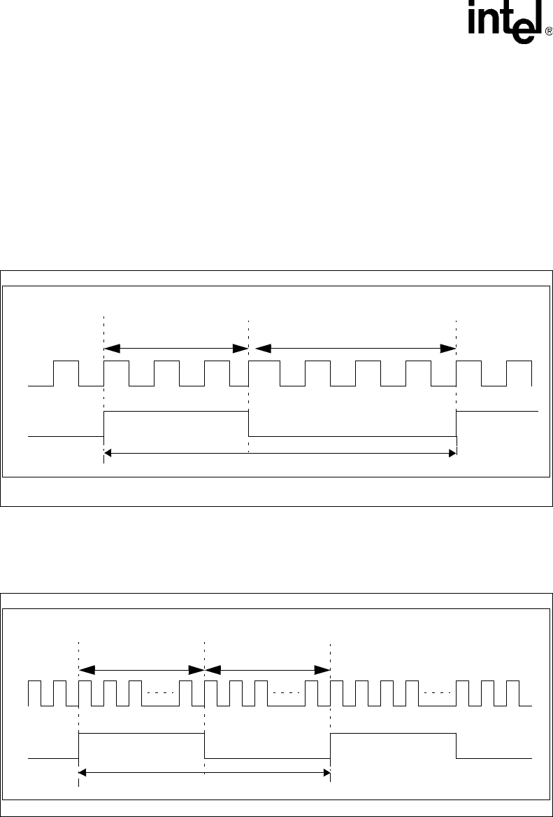
IXF1104 4-Port Gigabit Ethernet Media Access Controller
144 Datasheet
Document Number: 278757
Revision Number: 007
Revision Date: March 25, 2004
7.6 MDIO AC Timing Specification
The MDIO Interface on the IXF1104 can operate in two modes – low-speed and high-speed. In
low-speed mode, the MDC clock signal operates at a frequency of 2.5 MHz. In high-speed mode,
the MDC clock signal operates at a frequency of 18 MHz. (See Figure 41 through Figure 44 and
Table 52.)
7.6.1 MDC High-Speed Operation Timing
7.6.2 MDC Low-Speed Operation Timing
Figure 41. MDC High-Speed Operation Timing
Figure 42. MDC Low-Speed Operation Timing
24 ns
(3 X 125 MHz clocks) 32 ns
(4 X 125 MHz clocks)
MDC
56 ns (17.85 MHz)
200 ns
(25 X 125 MHz clocks) 200 ns
(25 X 125 MHz clocks)
MDC
400 ns (2.5 MHz)
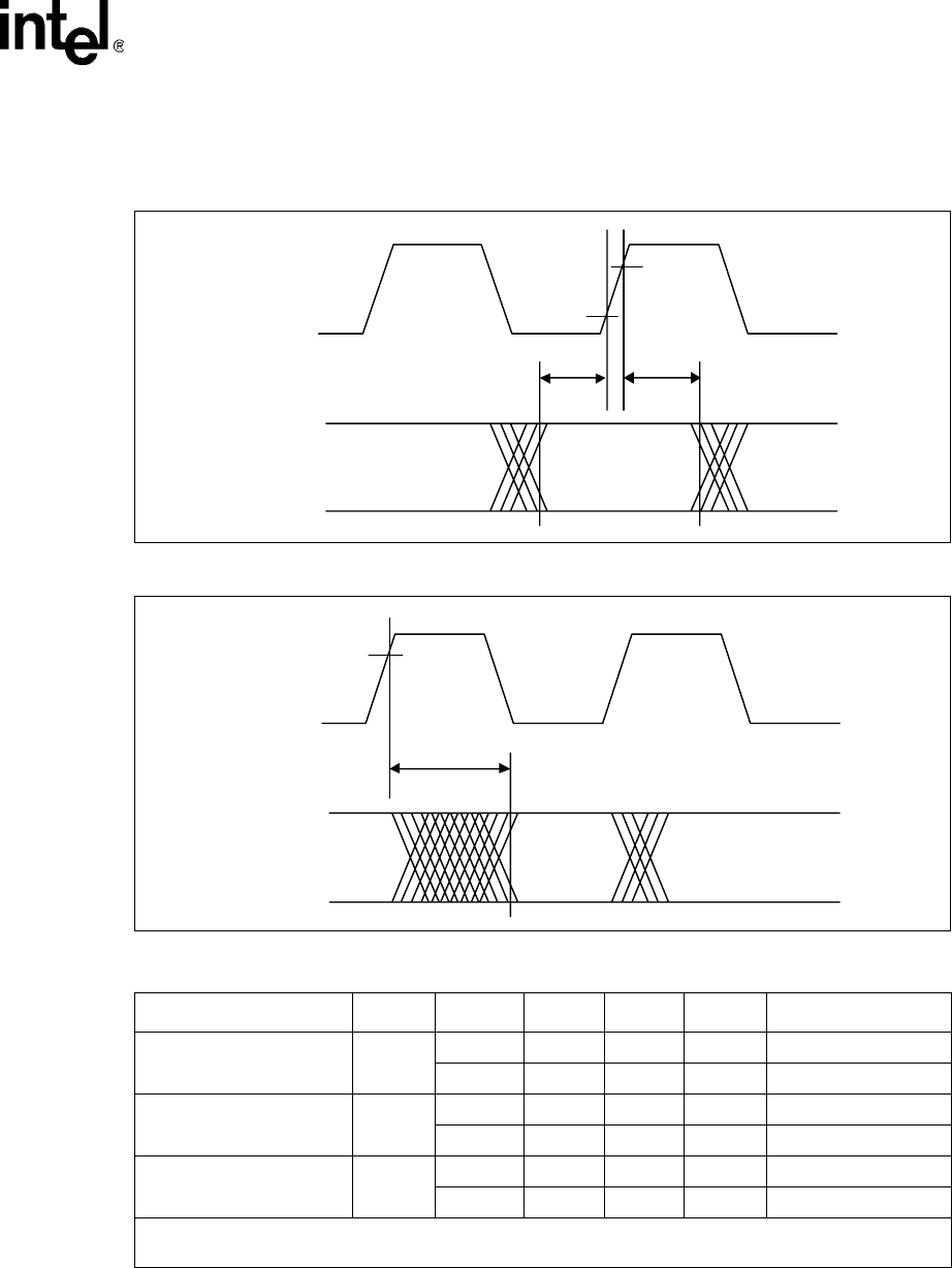
IXF1104 4-Port Gigabit Ethernet Media Access Controller
Datasheet 145
Document Number: 278757
Revision Number: 007
Revision Date: March 25, 2004
7.6.3 MDIO AC Timing
Figure 43. MDIO Write Timing Diagram
Figure 44. MDIO Read Timing Diagram
Table 52. MDIO Timing Parameters
Parameter Symbol Min Typ1Max Units Test Conditions
MDIO Setup before MDC. t1 10 – – ns MDC = 17.8 MHz
10 – – ns MDC = 2.5 MHz
MDIO Hold after MDC. t2 10 – – ns MDC = 17.8 MHz
10 – – ns MDC = 2.5 MHz
MDC to MDIO Output delay t3 0 – 42 ns MDC = 17.8 MHz
0 – 200 ns MDC = 2.5 MHz
1. Typical values are at 25 oC and are for design aid only; not guaranteed and not subject to production
testing.
t1
MDC
MDIO
t2
VMAX
VMIN
t3
MDC
MDIO
VMA X
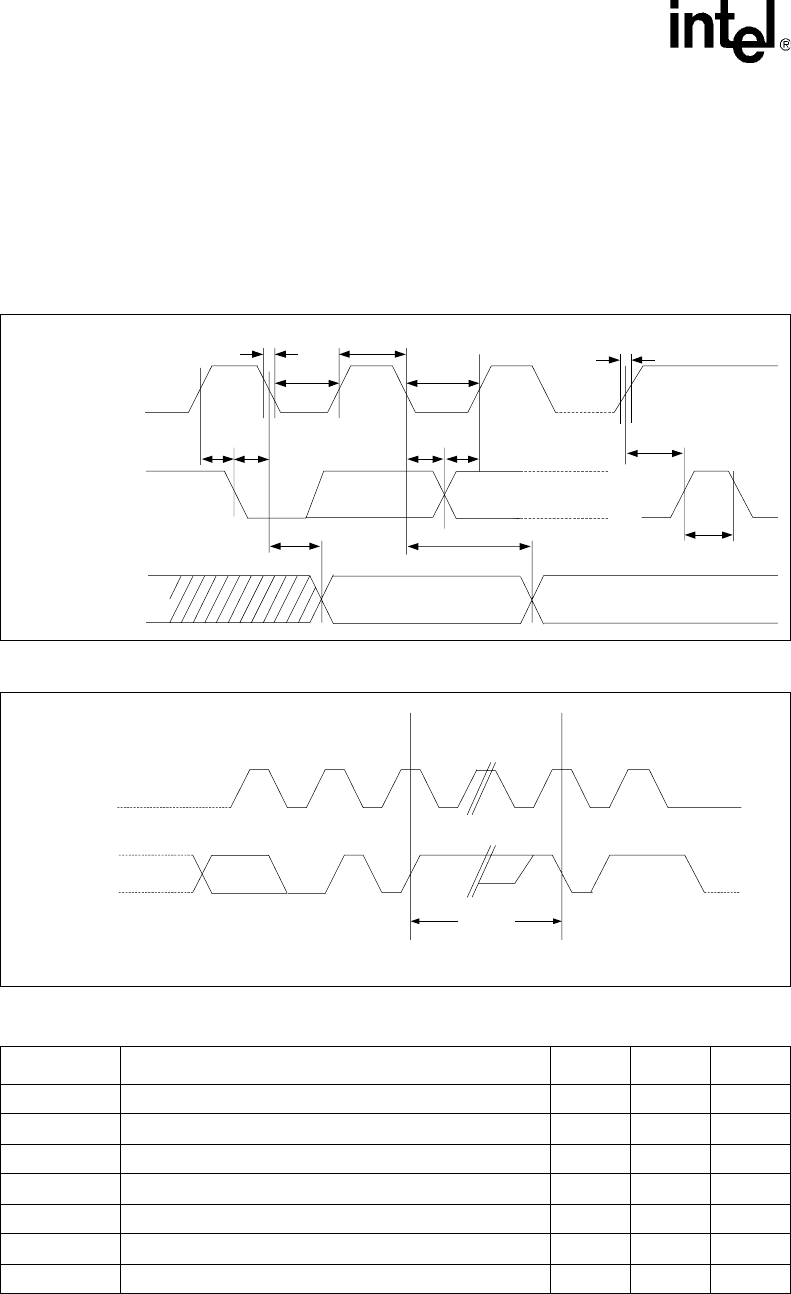
IXF1104 4-Port Gigabit Ethernet Media Access Controller
146 Datasheet
Document Number: 278757
Revision Number: 007
Revision Date: March 25, 2004
7.7 Optical Module and I2C AC Timing Specification
7.7.1 I2C Interface Timing
Figure 45 and Figure 46 illustrate bus timing and write cycle, and Table 53 shows the I2C Interface
AC timing characteristics.
Figure 45. Bus Timing Diagram
Figure 46. Write Cycle Diagram
Table 53. I2C AC Timing Characteristics (Sheet 1 of 2)
Symbol Parameter Min Max Units
fSCL Clock frequency, SCL - 100 kHz
tLOW Clock pulse width low 4.7 µs
tHIGH Clock pulse width High 4.0 µs
tINoise suppression 100 µs
tAA Clock low to data valid out 0.1 4.5 µs
tBUF Time the bus must be free before a new transmission starts 4.7 - µs
tHD.STA Start hold time 4.0 - µs
I2C_Clk
I2C_Data Out
tDH
tSV.SAT
tAA
tBUF
tHD.STA
tHIGH tR
tSU.STO
tSU.DAT
tHD.DAT
tLOW
tF
I2C_Data In
tLOW
ACK
8th
BIT
WORD n
I2C_Clk
I2C_Data
STOP
CONDITION START
CONDITION
tWR
(1)

IXF1104 4-Port Gigabit Ethernet Media Access Controller
Datasheet 147
Document Number: 278757
Revision Number: 007
Revision Date: March 25, 2004
tSU.STA Start setup time 4.7 – µs
tHD.DAT Data in hold time 0 – µs
tSU.DAT Data in setup time 200 – ns
tRInputs rise time – 1.0 µs
tFInputs fall time – 300 ns
tSU.STO Stop setup time 4.7 – µs
tDH Data out hold time 100 – ns
tWR Write cycle time – 10 ms
Table 53. I2C AC Timing Characteristics (Sheet 2 of 2)
Symbol Parameter Min Max Units
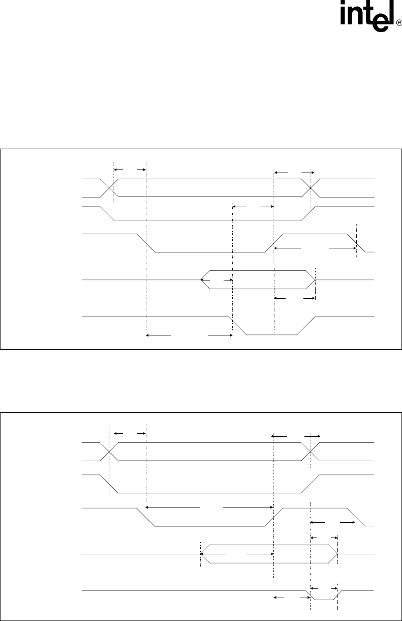
IXF1104 4-Port Gigabit Ethernet Media Access Controller
148 Datasheet
Document Number: 278757
Revision Number: 007
Revision Date: March 25, 2004
7.8 CPU AC Timing Specification
7.8.1 CPU Interface Read Cycle AC Timing
Figure 47, Figure 48, and Table 54 illustrate the CPU interface read and write cycle AC timing.
7.8.2 CPU Interface Write Cycle AC Timing
Figure 47. CPU Interface Read Cycle AC Timing
Figure 48. CPU Interface Write Cycle AC Timing
TCAS TCAH
TCRR
TCDRS
TCDRH
TCDRD
TCRH
uPx_ADD[12:0]
uPx_RdN
uPx_CsN
uPx_Data[31:0]
uPx_RdyN
TCAS TCAH
TCWL
TCDWS
TCDWD
TCYD
TCWH
uPx_Add[12:0]
uPx_WrN
uPx_CsN
uPx_Data[31:0]
uPx_RdyN
TCDWH

IXF1104 4-Port Gigabit Ethernet Media Access Controller
Datasheet 149
Document Number: 278757
Revision Number: 007
Revision Date: March 25, 2004
Table 54. CPU Interface Write Cycle AC Signal Parameters
Symbol Parameter Min Max
Tcas Address, chip select setup time 5 ns –
Tcah Address, chip select hold time 10 ns –
Tcrr Ready assertion to read de-assertion 10 ns –
Tcrh Read High width 24 ns –
Tcdrs Read data setup time to ready assertion 10 ns –
Tcdrh Read data hold time after read de-assertion 8 ns 32 ns
Tcdrd Read data driving delay 24 ns 355 ns
Tcwl Write assertion width 40 ns –
Tcwh Ready assertion to write assertion 16 ns –
Tcdws Write data setup to write de-assertion 10 ns –
Tcdwh Write data hold time after ready assertion 5 ns –
Tcdwd Write data sampling delay 8 ns 32 ns
Tcyd Ready width in write cycle 24 ns 40 ns
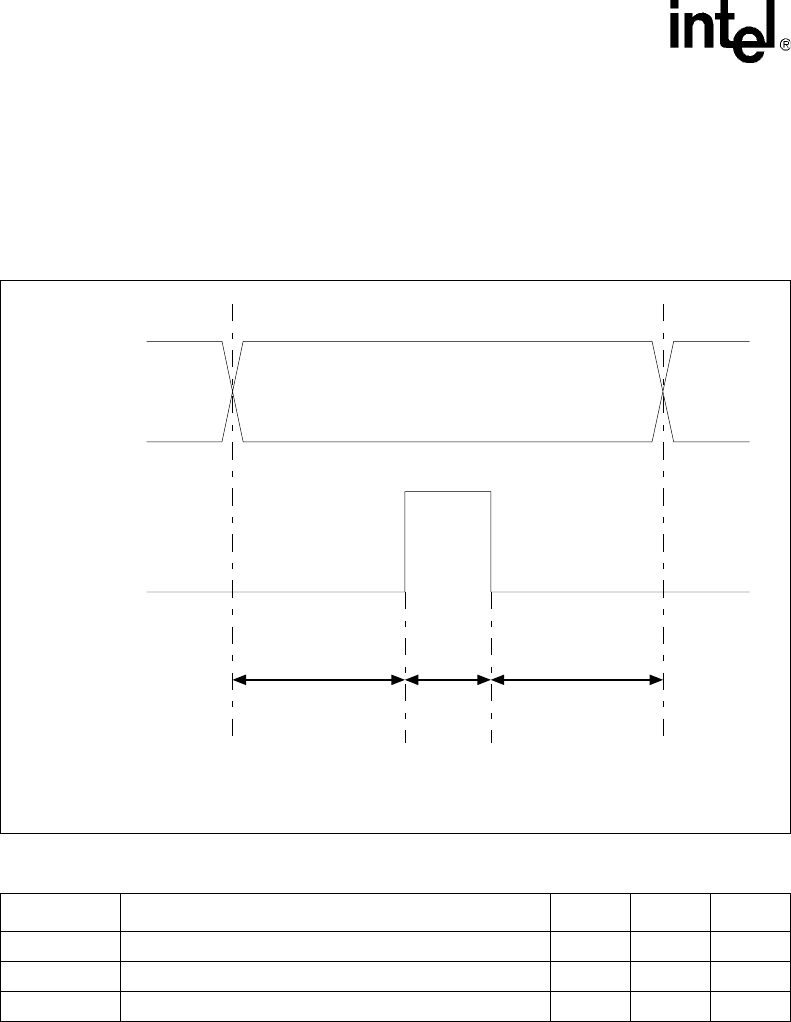
IXF1104 4-Port Gigabit Ethernet Media Access Controller
150 Datasheet
Document Number: 278757
Revision Number: 007
Revision Date: March 25, 2004
7.9 Transmit Pause Control AC Timing Specification
Figure 49 and Table 55 show the pause control AC timing specifications. The Pause Control
interface operates as an asynchronous interface relative to the main system clock (CLK125). There
is, however, a relationship between the TXPAUSEADD bus and the strobe signal (TXPAUSEFR).
Figure 49. Pause Control Interface Timing
Table 55. Transmit Pause Control Interface Timing Parameters
Symbol Parameter Min Max Units
Tsu TXPAUSEADD stable prior to TXPAUSEFR High 16 – ns
Tpw TXPAUSEFR pulse width 16 – ns
Thold TXPAUSEADD stable after TXPAUSEFR High 16 – ns
TxPauseAdd[1:0]
TxPauseFr
Tsu(min) = 16 ns Thold(min) = 16 ns
Tpw(min) = 16 ns
000 : XON packet on all ports
001 : XOFF Port0
010 : XOFF Port1
011 : XOFF Port2
100 : XOFF Port3
110-101 : Reserved
111 : XOFF on all ports
TXPAUSEADD[2:0]
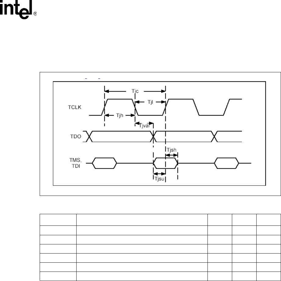
IXF1104 4-Port Gigabit Ethernet Media Access Controller
Datasheet 151
Document Number: 278757
Revision Number: 007
Revision Date: March 25, 2004
7.10 JTAG AC Timing Specification
Figure 50 and Table 56 provide the JTAG AC timing specifications.
Figure 50. JTAG AC Timing
Table 56. JTAG AC Timing Parameters
Symbol Parameter Min Max Units
Tjc TCLK cycle time 90 - ns
Tjh TCLK High time 0.4 x Tjc 0.6 x Tjc ns
Tjl TCLK low time 0.4 x Tjc 0.6 x Tjc ns
Tjval TCLK falling edge to TDO valid - 25 ns
Tjsu TMS/TDI setup to TCLK 20 - ns
Tjsh TMS/TDI hold from TCLK 5 - ns
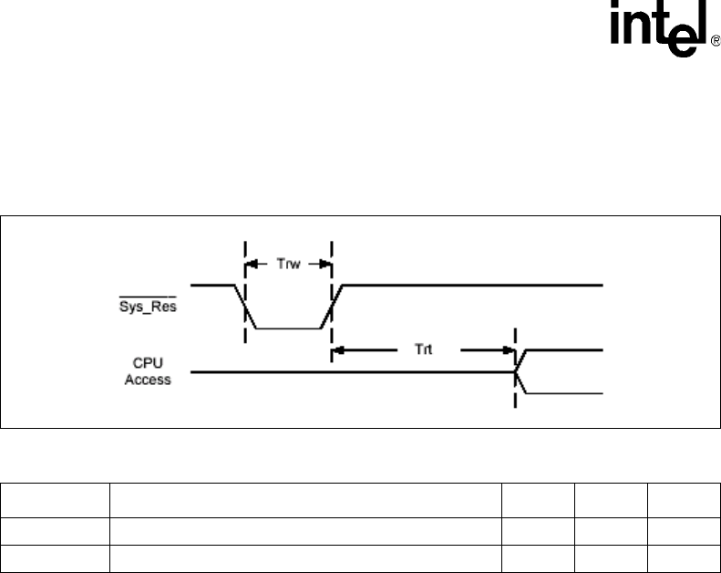
IXF1104 4-Port Gigabit Ethernet Media Access Controller
152 Datasheet
Document Number: 278757
Revision Number: 007
Revision Date: March 25, 2004
7.11 System AC Timing Specification
Figure 51 and Table 57 illustrate the system reset AC timing specifications.
Figure 51. System Reset AC Timing
Table 57. System Reset AC Timing Parameters
Symbol Parameter Min Max Units
Trw Reset pulse width 1.0 - µs
Trt Reset recovery time 200 - µs
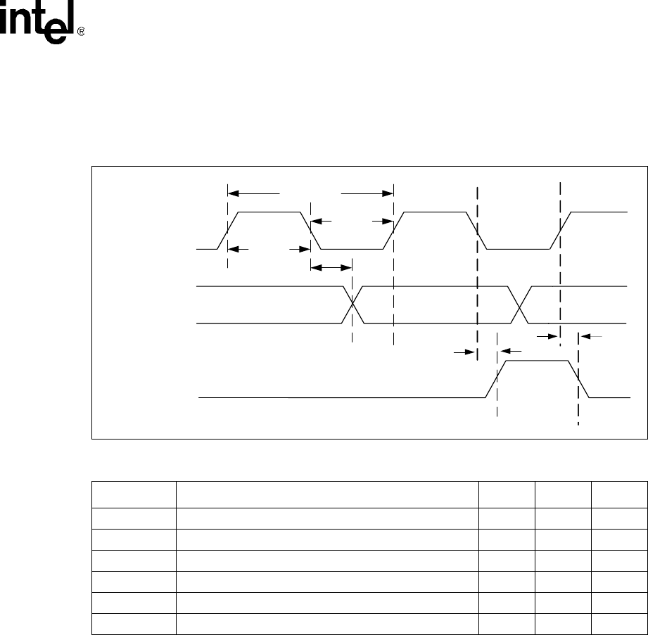
IXF1104 4-Port Gigabit Ethernet Media Access Controller
Datasheet 153
Document Number: 278757
Revision Number: 007
Revision Date: March 25, 2004
7.12 LED AC Timing Specification
Figure 52 and Table 58 provide the LED AC timing specifications.
Figure 52. LED AC Interface Timing
Table 58. LED Interface AC Timing Parameters
Symbol Parameter Min Max Units
Tcyc LED_CLK cycle time 1.36 1.40 ms
Thi LED_CLK High time 680 700 µs
Tlow LED_CLK low time 680 700 µs
Tdatd LED_CLK falling edge to LED_DATA valid 2 5 ns
Tlath LED_CLK rising edge to LED_LATCH rising edge 690 700 µs
Tlatl LED_CLK falling edge to LED_LATCH falling edge 690 700 µs
LED_CLK
LED_DATA
L
ED_LATCH
Tcyc
Tlow
Thi
Tdatd
Tha
tl
Tlath

IXF1104 4-Port Gigabit Ethernet Media Access Controller
154 Datasheet
Document Number: 278757
Revision Number: 007
Revision Date: March 25, 2004
8.0 Register Set
The registers shown in this section provide access for configuration, alarm monitoring, and control
of the chip. Table 59 “MAC Control Registers ($ Port Index + Offset)” on page 155 through
Table 69 “Optical Module Registers ($ 0x799 - 0x79F)” on page 161 provide register map details.
The registers are listed by ascending address in the table.
8.1 Document Structure
The following sections are structured to provide a general overview of the register map. Later
sections provide detailed descriptions of each register segment or bit.
All registers are accessed and addressed as 32-bit doublewords. When accessed using 8- or 16-bit
accesses, the CPU interface packs or unpacks the partial accesses into a 32-bit register value.
8.2 Graphical Representation
Figure 53 represents an overview of the IXF1104 global control status registers that are used to
configure or report on all ports. All register locations shown in Figure 53 represent a 32-bit double
word.
Figure 53. Memory Overview Diagram
B0744-01
Global Configuration
Reserved
Reserved
Reserved
Reserved
Reserved
Reserved
Port 3 MAC Control & Statistics
Port 2 MAC Control & Statistics
Port 1 MAC Control & Statistics
Port 0 MAC Control & Statistics
- RX Block Configuration
- TX Block Configuration
0x7FF
0x500
0x480
0x400
0x380
0x300
0x280
0x200
0x180
0x100
0x080
0x000

IXF1104 4-Port Gigabit Ethernet Media Access Controller
Datasheet 155
Document Number: 278757
Revision Number: 007
Revision Date: March 25, 2004
8.3 Per Port Registers
Section 8.4 covers all of the registers that are replicated in each port of the IXF1104. These
registers perform an identical function in each port.
The address vector for the IXF1104 is 11 bits wide. This allows for 7 bits of port-specific access
and a 4-bit vector to address each port and all global registers. The address format is shown in
Figure 54.
8.4 Register Map
Table 59 through Table 69 “Optical Module Registers ($ 0x799 - 0x79F)” on page 161 present the
IXF1104 memory map details. Global control and status registers are used to configure or report on
all ports, and some registers are replicated on a per-port basis.
Note: All IXF1104 registers are 32 bits.
Figure 54. Register Overview Diagram
Port Select & Global Registers Per-Port Registers
10 0
6
Table 59. MAC Control Registers ($ Port Index + Offset) (Sheet 1 of 2)
Register Bit Size Mode1Ref Page Offset
“Station Address ($ Port_Index +0x00 – +0x01)” Low 32 R/W 162 0x00
“Station Address ($ Port_Index +0x00 – +0x01)” High 32 R/W 162 0x01
“Desired Duplex ($ Port_Index + 0x02)” 32 R/W 162 0x02
“FD FC Type ($ Port_Index + 0x03)” 32 R/W 162 0x03
Reserved 32 R – 0x04
“Collision Distance ($ Port_Index + 0x05)” 32 R/W 163 0x05
“Collision Threshold ($ Port_Index + 0x06)” 32 R/W 163 0x06
“FC TX Timer Value ($ Port_Index + 0x07)” 32 R/W 163 0x07
“FD FC Address ($ Port_Index + 0x08 – + 0x09)”
FDFCAddressLow 32 R/W 163 0x08
“FD FC Address ($ Port_Index + 0x08 – + 0x09)”
FDFCAddressHigh 32 R/W 163 0x09
“IPG Receive Time 1 ($ Port_Index + 0x0A)” 32 R/W 164 0x0A
“IPG Receive Time 2 ($ Port_Index + 0x0B)” 32 R/W 164 0x0B
“IPG Transmit Time ($ Port_Index + 0x0C)” 32 R/W 164 0x0C
Reserved – RO – 0x0D
“Pause Threshold ($ Port_Index + 0x0E)” 32 R/W 165 0x0E

IXF1104 4-Port Gigabit Ethernet Media Access Controller
156 Datasheet
Document Number: 278757
Revision Number: 007
Revision Date: March 25, 2004
“Max Frame Size (Addr: Port_Index + 0x0F)” 32 R/W 165 0x0F
“MAC IF Mode and RGMII Speed ($ Port_Index + 0x10)” 32 R/W 166 0x10
“Flush TX ($ Port_Index + 0x11)” 32 R/W 166 0x11
“FC Enable ($ Port_Index + 0x12)” 32 R/W 167 0x12
“FC Back Pressure Length ($ Port_Index + 0x13)” 32 R/W 167 0x13
“Short Runts Threshold ($ Port_Index + 0x14)” 32 R/W 168 0x14
“Discard Unknown Control Frame ($ Port_Index +
0x15)” 32 R/W 168 0x15
“RX Config Word ($ Port_Index + 0x16)” 32 RO 168 0x16
“TX Config Word ($ Port_Index + 0x17)” 32 R/W 169 0x17
“Diverse Config Write ($ Port_Index + 0x18)” 32 R/W 170 0x18
“RX Packet Filter Control ($ Port_Index + 0x19)” 32 R/W 171 0x19
“Port Multicast Address ($ Port_Index +0x1A – +0x1B)”
PortMulticastAddressLow 32 R/W 172 0x1A
“Port Multicast Address ($ Port_Index +0x1A – +0x1B)”
PortMulticastAddressHigh 32 R/W 172 0x1B
Table 60. MAC RX Statistics Registers ($ Port Index + Offset) (Sheet 1 of 2)
Register Bit Size Mode1Ref Page Offset
RxOctetsTotalOK 32 R 173 0x20
RxOctetsBAD 32 R 173 0x21
RxUCPckts 32 R 173 0x22
RxMCPkts 32 R 173 0x23
RxBCPkts 32 R 173 0x24
RxPkts64Octets 32 R 173 0x25
RxPkts65to127Octets 32 R 173 0x26
RxPkts128to255Octets 32 R 173 0x27
RxPkts256to511Octets 32 R 173 0x28
RxPkts512to1023Octets 32 R 173 0x29
RxPkts1024to1518Octets 32 R 173 0x2A
RxPkts1519toMaxOctets 32 R 173 0x2B
RxFCSErrors 32 R 173 0x2C
RxTagged 32 R 173 0x2D
RxDataError 32 R 173 0x2E
RxAlign Errors 32 R 173 0x2F
RxLongErrors 32 R 173 0x30
RxJabberErrors 32 R 173 0x31
PauseMacControlReceivedCounter 32 R 173 0x32
Table 59. MAC Control Registers ($ Port Index + Offset) (Sheet 2 of 2)
Register Bit Size Mode1Ref Page Offset

IXF1104 4-Port Gigabit Ethernet Media Access Controller
Datasheet 157
Document Number: 278757
Revision Number: 007
Revision Date: March 25, 2004
RxUnknownMacControlFrameCounter 32 R 173 0x33
RxVeryLongErrors 32 R 173 0x34
RxRuntErrors 32 R 173 0x35
RxShortErrors 32 R 173 0x36
RxCarrierExtendError 32 R 173 0x37
RxSequenceErrors 32 R 173 0x38
RxSymbolErrors 32 R 173 0x39
Table 61. MAC TX Statistics Registers ($ Port Index + Offset)
Register Bit Size Mode1Ref Page Offset
OctetsTransmittedOK 32 R 177 0x40
OctetsTransmittedBad 32 R 177 0x41
TxUCPkts 32 R 177 0x42
TxMCPkts 32 R 177 0x43
TxBCPkts 32 R 177 0x44
TxPkts64Octets 32 R 177 0x45
TxPkts65to127Octets 32 R 177 0x46
TxPkts128to255Octets 32 R 177 0x47
TxPkts256to511Octets 32 R 177 0x48
TxPkts512to1023Octets 32 R 177 0x49
TxPkts1024to1518Octets 32 R 177 0x4A
TxPkts1519toMaxOctets 32 R 177 0x4B
TxDeferred 32 R 177 0x4C
TxTotalCollisions 32 R 177 0x4D
TxSingleCollisions 32 R 177 0x4E
TxMultipleCollisions 32 R 177 0x4F
TxLateCollisions 32 R 177 0x50
TxExcessiveCollisionErrors 32 R 177 0x51
TxExcessiveDeferralErrors 32 R 177 0x52
TxExcessiveLengthDrop 32 R 177 0x53
TxUnderrun 32 R 177 0x54
TxTagged 32 R 177 0x55
TxCRCError 32 R 177 0x56
TxPauseFrames 32 R 177 0x57
TxFlowControlCollisionsSend 32 R 177 0x58
Table 60. MAC RX Statistics Registers ($ Port Index + Offset) (Sheet 2 of 2)
Register Bit Size Mode1Ref Page Offset

IXF1104 4-Port Gigabit Ethernet Media Access Controller
158 Datasheet
Document Number: 278757
Revision Number: 007
Revision Date: March 25, 2004
Table 62. PHY Autoscan Registers ($ Port Index + Offset)
Register Bit Size Mode1Ref Page Offset
“PHY Control ($ Port Index + 0x60)” 32 RO 180 0x60
“PHY Status ($ Port Index + 0x61)” 32 RO 181 0x61
“PHY Identification 1 ($ Port Index + 0x62)” 32 RO 182 0x62
“PHY Identification 2 ($ Port Index + 0x63)” 32 RO 182 0x63
“Auto-Negotiation Advertisement ($ Port Index + 0x64)” 32 RO 183 0x64
“Auto-Negotiation Link Partner Base Page Ability ($ Port
Index + 0x65)” 32 RO 184 0x65
“Auto-Negotiation Expansion ($ Port Index + 0x66)” 32 RO 185 0x66
“Auto-Negotiation Next Page Transmit ($ Port Index +
0x67)” 32 RO 186 0x67
Reserved 32 RO – 0x68 - 0x6F
Table 63. Global Status and Configuration Registers ($ 0x500 - 0X50C)
Register Bit Size Mode1Ref Page Address
“Port Enable ($0x500)” 32 R/W 187 0x500
“Interface Mode ($0x501)” 32 R/W 187 0x501
“Link LED Enable ($0x502)” 32 R/W 188 0x502
Reserved 32 RO – 0x503 - 0x504
“MAC Soft Reset ($0x505)” 32 R/W 188 0x505
“MDIO Soft Reset ($0x506)” 32 R/W 189 0x506
Reserved 32 RO – 0x507
“CPU Interface ($0x508)” 32 R/W 189 0x508
“LED Control ($0x509)” 32 R/W 189 0x509
“LED Flash Rate ($0x50A)” 32 R/W 190 0x50A
“LED Fault Disable ($0x50B)” 32 R/W 190 0x50B
“JTAG ID ($0x50C)” 32 R 191 0x50C
Table 64. RX FIFO Registers ($ 0x580 - 0x5BF) (Sheet 1 of 2)
Register Bit Size Mode1Ref Page Address
“RX FIFO High Watermark Port 0 ($0x580)” 32 R/W 192 0x580
“RX FIFO High Watermark Port 1 ($0x581)” 32 R/W 192 0x581
“RX FIFO High Watermark Port 2 ($0x582)” 32 R/W 192 0x582
“RX FIFO High Watermark Port 3 ($0x583)” 32 R/W 193 0x583
Reserved 32 RO – 0x584 - 0x589
“RX FIFO Low Watermark Port 0 ($0x58A)” 32 R/W 193 0x58A
“RX FIFO Low Watermark Port 1 ($0x58B)” 32 R/W 193 0x58B
“RX FIFO Low Watermark Port 2 ($0x58C)” 32 R/W 194 0x58C

IXF1104 4-Port Gigabit Ethernet Media Access Controller
Datasheet 159
Document Number: 278757
Revision Number: 007
Revision Date: March 25, 2004
“RX FIFO Low Watermark Port 3 ($0x58D)” 32 R/W 194 0x58D
Reserved 32 RO – 0x58E - 0x593
RX FIFO Overflow Frame Drop Counter Port 0 32 R 194 0x594
RX FIFO Overflow Frame Drop Counter Port 1 32 R 194 0x595
RX FIFO Overflow Frame Drop Counter Port 2 32 R 194 0x596
RX FIFO Overflow Frame Drop Counter Port 3 32 R 194 0x597
Reserved 32 RO – 0x598 - 0x59D
“RX FIFO Port Reset ($0x59E)” 32 R/W 195 0x59E
“RX FIFO Errored Frame Drop Enable ($0x59F)” 32 R/W 195 0x59F
“RX FIFO Overflow Event ($0x5A0)” 32 R 196 0x5A0
Reserved 32 R – 0x5A1 - 0x5A5
RX FIFO Errored Frame Drop Counter Port 0 32 R 197 0x5A2
RX FIFO Errored Frame Drop Counter Port 1 32 R 197 0x5A3
RX FIFO Errored Frame Drop Counter Port 2 32 R 197 0x5A4
RX FIFO Errored Frame Drop Counter Port 3 32 R 197 0x5A5
Reserved 32 RO – 0x5A6 - 0x5B1
“RX FIFO SPI3 Loopback Enable for Ports 0 - 3
($0x5B2)” 32 R/W 198 0x5B2
“RX FIFO Padding and CRC Strip Enable ($0x5B3)” 32 R/W 199 0x5B3
Reserved 32 R – 0x5B4 - 0x5B7
“RX FIFO Transfer Threshold Port 0 ($0x5B8)” 32 R/W 200 0x5B8
“RX FIFO Transfer Threshold Port 1 ($0x5B9)” 32 R/W 200 0x5B9
“RX FIFO Transfer Threshold Port 2 ($0x5BA)” 32 R/W 200 0x5BA
“RX FIFO Transfer Threshold Port 3 ($0x5BB)” 32 R/W 201 0x5BB
Reserved 32 R – 0x5BC - 0x5BF
Table 65. TX FIFO Registers ($ 0x600 - 0x63E) (Sheet 1 of 2)
Register Bit Size Mode1Ref Page Address
TX FIFO High Watermark Port 0 32 R/W 202 0x600
TX FIFO High Watermark Port 1 32 R/W 202 0x601
TX FIFO High Watermark Port 2 32 R/W 202 0x602
TX FIFO High Watermark Port 3 32 R/W 202 0x603
Reserved 32 RO – 0x604 - 0x609
TX FIFO Low Watermark Port 0 32 R/W 203 0x60A
TX FIFO Low Watermark Port 1 32 R/W 203 0x60B
TX FIFO Low Watermark Port 2 32 R/W 203 0x60C
TX FIFO Low Watermark Port 3 32 R/W 203 0x60D
Table 64. RX FIFO Registers ($ 0x580 - 0x5BF) (Sheet 2 of 2)
Register Bit Size Mode1Ref Page Address

IXF1104 4-Port Gigabit Ethernet Media Access Controller
160 Datasheet
Document Number: 278757
Revision Number: 007
Revision Date: March 25, 2004
Reserved 32 RO – 0x60E - 0x613
TX FIFO MAC Threshold Port 0 32 R/W 204 0x614
TX FIFO MAC Threshold Port 1 32 R/W 204 0x615
TX FIFO MAC Threshold Port 2 32 R/W 204 0x616
TX FIFO MAC Threshold Port 3 32 R/W 204 0x617
Reserved – RO – 0x618 - 0x61D
TX FIFO Overflow/Underflow Event/Out of Sequence 32 R 205 0x61E
Loop RX Data to TX FIFO 32 R/W 206 0x61F
TX FIFO Port Reset 32 R/W 206 0x620
TX FIFO Overflow Frame Drop Counter Port 0 32 R 207 0x621
TX FIFO Overflow Frame Drop Counter Port 1 32 R 207 0x622
TX FIFO Overflow Frame Drop Counter Port 2 32 R 207 0x623
TX FIFO Overflow Frame Drop Counter Port 3 32 R 207 0x624
TX FIFO Errored Frame Drop Counter Port 0 32 R 208 0x625
TX FIFO Errored Frame Drop Counter Port 1 32 R 208 0x626
TX FIFO Errored Frame Drop Counter Port 2 32 R 208 0x627
TX FIFO Errored Frame Drop Counter Port 3 32 R 208 0x628
Reserved 32 R – 0x629 - 0x62C
TX FIFO Occupancy Counter for Port 0 32 R 209 0x62D
TX FIFO Occupancy Counter for Port 1 32 R 209 0x62E
TX FIFO Occupancy Counter for Port 2 32 R 209 0x62F
TX FIFO Occupancy Counter for Port 3 32 R 209 0x630
Reserved 32 R – 0x631 - 0x63E
Table 66. MDIO Registers ($ 0x680 - 0x683)
Register Bit Size Mode1Ref Page Address
“MDIO Single Command ($0x680)” 32 R/W 210 0x680
“MDIO Single Read and Write Data ($0x681)” 32 R/W 210 0x681
“Autoscan PHY Address Enable ($0x682)” 32 R/W 211 0x682
“MDIO Control ($0x683)” 32 R/W 211 0x683
Table 67. SPI3 Registers ($ 0x700 - 0x716) (Sheet 1 of 2)
Register Bit Size Mode1Ref Page Address
“SPI3 Transmit and Global Configuration ($0x700)” 32 R/W 212 0x700
“SPI3 Receive Configuration ($0x701)” 32 R/W 214 0x701
Table 65. TX FIFO Registers ($ 0x600 - 0x63E) (Sheet 2 of 2)
Register Bit Size Mode1Ref Page Address

IXF1104 4-Port Gigabit Ethernet Media Access Controller
Datasheet 161
Document Number: 278757
Revision Number: 007
Revision Date: March 25, 2004
Reserved 32 R – 0x702 - 0x709
“Address Parity Error Packet Drop Counter ($0x70A)” 32 R 218 0x70A
Reserved 32 R – 0x70B - 0x716
Table 68. SerDes Registers ($ 0x780 - 0x798)
Register Bit Size Mode1Ref Page Address
Reserved 32 RO – 0x780 - 0x783
“TX Driver Power Level Ports 0 - 3 ($0x784)” 32 R/W 219 0x784
Reserved 32 RO – 0x785 - 0x786
“TX and RX Power-Down ($0x787)" 32 R/W 219 0x787
Reserved 32 RO – 0x788 - 0x792
“RX Signal Detect Level Ports 0 - 3 ($0x793)” 32 R/W 219 0x793
“Clock and Interface Mode Change Enable Ports 0 - 3
($0x794)” 32 R/W 220 0x794
Reserved 32 RO – 0x795 - 0x798
Table 69. Optical Module Registers ($ 0x799 - 0x79F)
Register Bit Size Mode1Ref Page Address
“Optical Module Status Ports 0-3 ($0x799)” 32 R 221 0x799
“Optical Module Control Ports 0 - 3 ($0x79A)” 32 R/W 221 0x79A
“I2C Control Ports 0 - 3 ($0x79B)” 32 R/W 222 0x79B
Reserved 32 RO – 0x79C - 0x79E
“I2C Data Ports 0 - 3 ($0x79F)” 32 R/W 222 0x79F
Table 67. SPI3 Registers ($ 0x700 - 0x716) (Sheet 2 of 2)
Register Bit Size Mode1Ref Page Address

IXF1104 4-Port Gigabit Ethernet Media Access Controller
162 Datasheet
Document Number: 278757
Revision Number: 007
Revision Date: March 25, 2004
8.4.1 MAC Control Registers
Table 70 through Table 92 “Port Multicast Address ($ Port_Index +0x1A – +0x1B)” on page 172
provide details on the control and status registers associated with each MAC port. The register
address is ‘Port_index + 0x**’, where the port index is set at any value from 0x0 through 0x5. All
registers are 32-bit. The unused bits of the registers are read-only and are set permanently to zero.
Table 70. Station Address ($ Port_Index +0x00 – +0x01)
Name Description Address Type1Default
Station Address
Low
Source MAC address bit 31-0.
This address is inserted in the source address
field when transmitting pause frames, and is also
used to compare against unicast pause frames
at the receiving side.
Port_Index
+ 0x00 R/W 0x0000000
Station Address
High
Source MAC address bit 47-32.
This address is inserted in the source address
field when transmitting pause frames, and is also
used to compare against unicast pause frames
at the receiving side. Bits 15:0 of this register are
assigned to bits 47:32 of the station address.
Port_Index
+ 0x01 R/W 0x00000000
1. RO = Read Only, No clear on Read; R = Read, Clear on Read; W = Write only; R/W = Read/Write, No
clear; R/W/C = Read/Write, Clear on Write
Table 71. Desired Duplex ($ Port_Index + 0x02)
Bit Name Description Type1Default
Register Description: Chooses between half-duplex and full-duplex operation in RGMII
100 Mbps or 10 Mbps mode only.
This register must be set to the default value of 1 and must not be changed when operating in
RGMII 1000 Mbps, GMII, or fiber mode.
0x00000001
31:1 Reserved Reserved R 0x00000000
0 Duplex Select
0 = Half-duplex
1 = Full-duplex
NOTE: Half-duplex operation applies only to
10/100 Mbps speed on copper media in RGMII
mode only. Gigabit speed on either media requires
full-duplex.
R/W 1
1. RO = Read Only, No clear on Read; R = Read, Clear on Read; W = Write only; R/W = Read/Write, No
clear; R/W/C = Read/Write, Clear on Write
Table 72. FD FC Type ($ Port_Index + 0x03)
Name Description Address Type1Default
FD FC Type This value fills the Type field of the Transmitted
Pause frames. Only bits 15:0 of this register are
used.
Port_Index
+ 0x03 R/W 0x00008808
1. RO = Read Only, No clear on Read; R = Read, Clear on Read; W = Write only; R/W = Read/Write, No
clear; R/W/C = Read/Write, Clear on Write

IXF1104 4-Port Gigabit Ethernet Media Access Controller
Datasheet 163
Document Number: 278757
Revision Number: 007
Revision Date: March 25, 2004
Table 73. Collision Distance ($ Port_Index + 0x05)
Name Description Address Type1Default
Collision
Distance
This is a 10-bit value that sets the limit for late
collision. Collisions happening at byte times
beyond the configured value are considered to be
late collisions. (Only valid in half-duplex).
Port_Index
+ 0x05 R/W 0x00000043
1. RO = Read Only, No clear on Read; R = Read, Clear on Read; W = Write only; R/W = Read/Write, No clear;
R/W/C = Read/Write, Clear on Write
Table 74. Collision Threshold ($ Port_Index + 0x06)
Name Description Address Type1Default
Collision
Threshold
This is a 4-bit value that sets the limit for
excessive collisions. When the number of
transmission attempts performed for a packet
exceeds this value, it is considered to be an
excessive collision and the frame is dropped.
(Only valid in half-duplex).
Port_Index
+ 0x06 R/W 0x0000000F
1. RO = Read Only, No clear on Read; R = Read, Clear on Read; W = Write only; R/W = Read/Write, No clear;
R/W/C = Read/Write, Clear on Write
Table 75. FC TX Timer Value ($ Port_Index + 0x07)
Name Description Address Type1Default
FC TX Timer
Value
The 16-bit pause length inserted in the flow
control pause frame sent to the receiving
station. The value is in 512-bit times.
Port_Index
+ 0x07 R/W 0x0000005E
1. RO = Read Only, No clear on Read; R = Read, Clear on Read; W = Write only; R/W = Read/Write, No
clear; R/W/C = Read/Write, Clear on Write
Table 76. FD FC Address ($ Port_Index + 0x08 – + 0x09)
Name Description Address Type1Default
FD FC Address Low The lowest 32 bits of the 48-bit globally
assigned multicast pause frame destination
address.
Port_Index
+ 0x08 R/W 0xC2000001
FD FC Address High
The highest 16 bits (47:32) of the globally
assigned multicast pause frame destination
address. The higher 16-bit address is
derived from bits 15:0 of this register.
Port_Index
+ 0x09 R/W 0x00000180
1. RO = Read Only, No clear on Read; R = Read, Clear on Read; W = Write only; R/W = Read/Write, No
clear; R/W/C = Read/Write, Clear on Write

IXF1104 4-Port Gigabit Ethernet Media Access Controller
164 Datasheet
Document Number: 278757
Revision Number: 007
Revision Date: March 25, 2004
Table 77. IPG Receive Time 1 ($ Port_Index + 0x0A)
Name Description Address Type1Default
IPG Receive Time 1
This timer is used during half-duplex operation
when there is a packet waiting for
transmission from the MAC. This timer starts
after CRS is de-asserted. If CRS is asserted
during this time, no transmission is initiated
and the counter restarts once CRS is de-
asserted again.
The value specified in this register is
calculated as follows: (register_value * 8) =
RXIPG1 in terms of bit times. Therefore, a
default value of 8 gives the following: (8 * 8 =
64 bit times for the default).
Port_Index
+ 0x0A R/W 0x00000008
1. RO = Read Only, No clear on Read; R = Read, Clear on Read; W = Write only; R/W = Read/Write, No
clear; R/W/C = Read/Write, Clear on Write
Table 78. IPG Receive Time 2 ($ Port_Index + 0x0B)
Name Description Address Type1Default
IPG Receive Time 2
This is only used in half-duplex operation. It
starts counting at the same time as RXIPG1.
Once RXIPG1 expires, a frame is transmitted
when RXIPG2 expires regardless of the CRS
value. If CRS is asserted before RXIPG1
expires, no transmission occurs and both
RXIPG1 an RXIPG2 are reset once CRS is
de-asserted again.
The value specified in this register is
calculated as follows: (register_value +5) * 8 =
RXIPG2 in terms of bit times. Therefore, a
default of 7 gives the following:
(7+5) * 8 = 96 bit times for default.
Port_Index
+ 0x0B R/W 0x00000007
1. RO = Read Only, No clear on Read; R = Read, Clear on Read; W = Write only; R/W = Read/Write, No
clear; R/W/C = Read/Write, Clear on Write
Table 79. IPG Transmit Time ($ Port_Index + 0x0C)
Name Description Address Type1Default
IPG Transmit Time
This is a 10-bit value configuring IPG time for
back-to-back transmissions.
The value specified in this register is
calculated as follows: (register_value +4) * 8 =
TXIPG in terms of bit times. Therefore, a
default value of 8 gives the following:
(8+4) * 8 = 96 bit times for the default.
Port_Index
+ 0x0C R/W 0x00000008
1. RO = Read Only, No clear on Read; R = Read, Clear on Read; W = Write only; R/W = Read/Write, No
clear; R/W/C = Read/Write, Clear on Write

IXF1104 4-Port Gigabit Ethernet Media Access Controller
Datasheet 165
Document Number: 278757
Revision Number: 007
Revision Date: March 25, 2004
Table 80. Pause Threshold ($ Port_Index + 0x0E)
Name Description Address Type1Default
Pause
Threshold
When a pause frame has been sent, an internal
timer checks when the next pause frame must
be scheduled for transmission to keep the link
partner in pause mode (this is required only if
the flow control has to be extended for one more
session). The pause threshold value is a 16-bit
value that sets the time in terms of 512-bit
quantum after the previous pause frame when
the next pause frame has to be sent. This
ensures that the link partner is kept in pause
mode continuously.
Port_Index
+ 0x0E R/W 0x0000002F
1. RO = Read Only, No clear on Read; R = Read, Clear on Read; W = Write only; R/W = Read/Write, No
clear; R/W/C = Read/Write, Clear on Write
Table 81. Max Frame Size (Addr: Port_Index + 0x0F)
Name Description Address Type1Default
Max Frame Size
This is a 14-bit value configuring the maximum
frame size the MAC can receive or transmit
without activating any error counters, and
without truncation.
This value is excluding the 4-byte CRC in the
transmit direction when CRC append is
enabled in the MAC. Hence, this value has to
be set four bytes less when CRC append is
enabled in the MAC.
The maximum frame size is internally adjusted
by +4 if the frame is VLAN tagged.
Port_Inde
x + 0x0F R/W 0x000005EE
1. RO = Read Only, No clear on Read; R = Read, Clear on Read; W = Write only; R/W = Read/Write, No
clear; R/W/C = Read/Write, Clear on Write

IXF1104 4-Port Gigabit Ethernet Media Access Controller
166 Datasheet
Document Number: 278757
Revision Number: 007
Revision Date: March 25, 2004
Table 82. MAC IF Mode and RGMII Speed ($ Port_Index + 0x10)
Bit Name Description Type1Default
Register Description – MAC IF Mode: Determines the MAC operation frequency and mode
per port.
Changes to the data setting of this register must be made in conjunction with the “Clock and
Interface Mode Change Enable Ports 0 - 3 ($0x794)" to ensure a safe transition to a new
operational mode. Changes to this register must follow a proper sequence. Refer to Section
6.1, “Change Port Mode Initialization Sequence” on page 129 for the proper sequence for
changing the port mode and speed.
0x00000003
31:3 Reserved Reserved R 0x00000000
2:0 Port Mode
These bits are used to define the clock mode and
the RGMII/GMII mode of operation.
000 = Reserved
001 = Reserved
010 = GMII 1000 Mbps operation
011 = Reserved
100 = RGMII 10 Mbps operation
101 = RGMII 100 Mbps operation
11x = RGMII 1000 Mbps operation
R/W 011
1. RO = Read Only, No clear on Read; R = Read, Clear on Read; W = Write only; R/W = Read/Write, No
clear; R/W/C = Read/Write, Clear on Write
Table 83. Flush TX ($ Port_Index + 0x11)
Bit Name Description Type1Default
Register Description: Used to flush all TX data. It is used if all traffic sent to a port should be
stopped. 0x00000000
31:1 Reserved Reserved R 0x00000000
0Flush TX This bit flushes all TX data and is used if all the
traffic sent to a port should be stopped. R/W 0
1. RO = Read Only, No clear on Read; R = Read, Clear on Read; W = Write only; R/W = Read/Write, No
clear; R/W/C = Read/Write, Clear on Write

IXF1104 4-Port Gigabit Ethernet Media Access Controller
Datasheet 167
Document Number: 278757
Revision Number: 007
Revision Date: March 25, 2004
Table 84. FC Enable ($ Port_Index + 0x12)
Bit Name Description Type1Default
Register Description: Indicates which flow control mode is used for the RX and TX MAC. 0x00000007
31:3 Reserved Reserved R 0x00000000
2TX HDFC
When TX HDFC is enabled (half-duplex mode
only), the MAC generates deliberate collisions on
incoming packets when the RX FIFO occupancy
crosses the High Watermark (flow control).
0 = Disable TX half-duplex flow control
1 = Enable TX half-duplex flow control
R/W 1
1TX FDFC
0 = Disable TX full-duplex flow control [the MAC
will not generate internally any flow control
frames based on the RX FIFO watermarks or
the Transmit Pause Control interface
1 = Enable TX full-duplex flow control [enables
the MAC to send flow control frames to the
link partner based on the RX FIFO
programmable watermarks or the Transmit
Pause Control interface]
R/W 1
0RX FDFC
0 = Disable RX full-duplex flow control [the MAC
will not respond to flow control frames sent to
it by the link partner]
1 = Enable RX full-duplex flow control [MAC will
respond to flow control frames sent by the link
partner and will stop packet transmission for
the time specified in the flow control frame]
R/W 1
1. RO = Read Only, No clear on Read; R = Read, Clear on Read; W = Write only; R/W = Read/Write, No
clear; R/W/C = Read/Write, Clear on Write
Table 85. FC Back Pressure Length ($ Port_Index + 0x13)
Name Description Address Type1Default
FC Back Pressure
Length
This register sets number the byte cycles
for which the collision has to be applied.
The 6-bit configuration holds the value in
bytes, which applies to the minimum
length/duration of back pressure in half-
duplex mode. Flow control in the receive
path is executed by deliberately colliding
the incoming packets in half-duplex mode.
Register bits 5:0 are used alone.
Port Add +
0x13 R/W 0x0000000C
1. RO = Read Only, No clear on Read; R = Read, Clear on Read; W = Write only; R/W = Read/Write, No
clear; R/W/C = Read/Write, Clear on Write

IXF1104 4-Port Gigabit Ethernet Media Access Controller
168 Datasheet
Document Number: 278757
Revision Number: 007
Revision Date: March 25, 2004
Table 86. Short Runts Threshold ($ Port_Index + 0x14)
Name Description Address Type1Default
Short Runts
Threshold
The 5-bit configuration holds the value in bytes,
which applies to the threshold in determining
between runts and short. The bits 4:0 of this
register are alone used.
A received packet is reported as a short packet
when the length (excluding Preamble and
SFD) is less than this value.
A received packet is reported as a runt packet
when the length (excluding Preamble and
SFD) is equal to or greater than this value and
less than 64-bytes.
NOTE: This register is only relevant when the
IXF1104 port is configured for copper
operation (the line side interface is
configured for either RGMII or GMII).
Port_Index +
0x14 R/W 0x00000008
1. RO = Read Only, No clear on Read; R = Read, Clear on Read; W = Write only; R/W = Read/Write, No
clear; R/W/C = Read/Write, Clear on Write
Table 87. Discard Unknown Control Frame ($ Port_Index + 0x15)
Bit Name Description Type1Default
Register Description: Discards or forwards unknown control frames. Known control frames
are pause frames. 0x00000000
31:1 Reserved Reserved R 0x00000000
0Discard Unknown
Control Frame 0 = Forward unknown control frames
1 = Discard unknown control frames R/W 0
1. RO = Read Only, No clear on Read; R = Read, Clear on Read; W = Write only; R/W = Read/Write, No
clear; R/W/C = Read/Write, Clear on Write
Table 88. RX Config Word ($ Port_Index + 0x16) (Sheet 1 of 2)
Bit Name Description Type1Default
Register Description: This register is used in fiber MAC only for auto-negotiation and to report
the receive status. The lower 16 bits of this register are the “config_reg” received from the link
partner, as described in IEEE 802.3 2000 Edition, Section 37.2.1. 0x00000000
31:22 Reserved Reserved RO 0x000
21 An_complete
Auto-negotiation complete. This bit remains
cleared from the time auto-negotiation is reset until
auto-negotiation reaches the “LINK_OK” state. It
remains set until auto-negotiation is disabled or
restarted.
This bit is only valid if auto-negotiation is enabled.
RO 0
20 Rx Sync 0 = Loss of synchronization
1 = Bit synchronization. The bit remains Low until
the register is read. RO 0
1. RO = Read Only, No clear on Read; R = Read, Clear on Read; W = Write only; R/W = Read/Write, No clear;
R/W/C = Read/Write, Clear on Write

IXF1104 4-Port Gigabit Ethernet Media Access Controller
Datasheet 169
Document Number: 278757
Revision Number: 007
Revision Date: March 25, 2004
19 RX Config 0 = Receiving idle/data stream
1 = Receiving /C/ ordered sets RO 0
18 Config Changed
0 = RxConfigWord has changed since last read
1 = RxConfigWord has not changed since last
read.
This bit remains High until the register is read.
R0
17 Invalid Word
0 = Have not received an invalid symbol
1 = Have received an invalid symbol
This bit remains High until the register is read.
RO 0
16 Carrier Sense
0 = Device is not receiving idle characters; carrier
sense is true.
1 = Device is receiving idle characters; carrier
sense is false.
RO 0
15 Next Page Next Page request RO 0
14 Reserved Reserved RO 0
13:122Remote Fault [1:0]
Remote fault definitions:
00 = No error, link okay
01 =Offline
10 =Link failure
11 = Auto-negotiation_Error
R/W 00
11:9 Reserved Reserved RO 000
8 Asym Pause Asym Pause. The ability to send pause frames. RO 0
7Sym Pause Sym Pause. The ability to send and receive pause
frames. RO 0
6 Half Duplex Half-duplex RO 0
5 Full Duplex Full-duplex RO 0
4:0 Reserved Reserved RO 0x0
Table 89. TX Config Word ($ Port_Index + 0x17) (Sheet 1 of 2)
Bit Name Description Type1Default
Register Description: This register is used in fiber MAC for auto-negotiation only. The
contents of this register are sent as the config_word. The contents of this register are the
“config_reg” sent to the link partner, as described in IEEE 802.3 2000 Edition, subclause 37.2.1. 0x0001A0
31:16 Reserved Reserved RO 0x0000
15 Next Page Next Page request R/W 0
14 Reserved Write as 0, ignore on read R/W 0
1. RO = Read Only, No clear on Read; R = Read, Clear on Read; W = Write only; R/W = Read/Write, No clear;
R/W/C = Read/Write, Clear on Write
NOTE: A value of 0x0 must be written to all reserved bits of the “TX Config Word ($ Port_Index + 0x17)”
Register.
Table 88. RX Config Word ($ Port_Index + 0x16) (Sheet 2 of 2)
Bit Name Description Type1Default
1. RO = Read Only, No clear on Read; R = Read, Clear on Read; W = Write only; R/W = Read/Write, No clear;
R/W/C = Read/Write, Clear on Write

IXF1104 4-Port Gigabit Ethernet Media Access Controller
170 Datasheet
Document Number: 278757
Revision Number: 007
Revision Date: March 25, 2004
13:122Remote Fault [1:0]
Remote fault definitions:
00 = No error, link okay
01 = Offline
10 = Link failure
11 = Auto-negotiation_Error
R/W 00
11:9 Reserved Write as 0, ignore on Read R/W 000
8 Asym Pause Asym Pause. The ability to send pause frames. R/W 1
7Sym Pause Sym Pause. The ability to send and receive pause
frames. R/W 1
6 Half Duplex Half-duplex R/W 1
5 Full Duplex Full-duplex R/W 1
4:0 Reserved Write as 0, ignore on read R/W 0x00
Table 90. Diverse Config Write ($ Port_Index + 0x18) (Sheet 1 of 2)
Bit Name Description Type1Default
Register Description: This register contains various configuration bits for general use. 0x00110D
31:19 Reserved Reserved RO 0x0000
18:13 Reserved Write as 0, ignore on Read. R/W 0x0000
12 Reserved2Write as 1, ignore on Read. R/W 1
11-9 Reserved2Write as 0, ignore on Read. R/W 0x0
8Reserved
2Write as 1, ignore on Read. R/W 1
7 pad_enable
0 = Normal operation
1 = Enable padding of undersized packets
NOTE: Assertion of this bit results in the
automatic addition of a CRC to the
padded packet.
R/W 0
6 crc_add 0 = Normal operation
1 = Enable automatic CRC appending R/W 0
5AN_enable
Enable auto-negotiation (used for fiber mode only)
to be performed by the hardware state machines
in the MAC.
The hardware auto-negotiation (AN) state
machine controls the config words transmitted
when this bit is set.
NOTE: In copper mode, this bit must be set to 0
(reserved).
R/W 0
42Reserved Write as 0, ignore on Read. R/W 0
1. RO = Read Only, No clear on Read; R = Read, Clear on Read; W = Write only; R/W = Read/Write, No clear;
R/W/C = Read/Write, Clear on Write
2. Reserved bits must be written to the default value for proper operation.
Table 89. TX Config Word ($ Port_Index + 0x17) (Sheet 2 of 2)
Bit Name Description Type1Default
1. RO = Read Only, No clear on Read; R = Read, Clear on Read; W = Write only; R/W = Read/Write, No clear;
R/W/C = Read/Write, Clear on Write
NOTE: A value of 0x0 must be written to all reserved bits of the “TX Config Word ($ Port_Index + 0x17)”
Register.

IXF1104 4-Port Gigabit Ethernet Media Access Controller
Datasheet 171
Document Number: 278757
Revision Number: 007
Revision Date: March 25, 2004
3:22Reserved Write as 1, ignore on Read. R/W 11
12Reserved Write as 0, ignore on Read. R/W 0
02Reserved Write as 1, ignore on Read. R/W 1
Table 90. Diverse Config Write ($ Port_Index + 0x18) (Sheet 2 of 2)
Bit Name Description Type1Default
1. RO = Read Only, No clear on Read; R = Read, Clear on Read; W = Write only; R/W = Read/Write, No clear;
R/W/C = Read/Write, Clear on Write
2. Reserved bits must be written to the default value for proper operation.
Table 91. RX Packet Filter Control ($ Port_Index + 0x19) (Sheet 1 of 2)
Bit Name Description Type1Default
Register Description: This register allows for specific packet types to be marked for filtering
and is used in conjunction with the “RX FIFO Errored Frame Drop Counter Ports 0 - 3 ($0x5A2
- 0x5A5)”.0x00000000
31:6 Reserved Reserved 0
5 CRC Error Pass
This bit enables a Global filter on frames with a
CRC Error.
0 = When CRC Error Pass = 0, all frames with a
CRC Error are marked as bad.2
1 = Frames with a CRC Error are not marked as
bad and are passed to the SPI3 interface for
transfer as good frames, regardless of the
state of the bits in the “RX FIFO Errored
Frame Drop Enable ($0x59F)”.
NOTE: When the CRC Error Pass Filter bit = 0, it
takes precedence over the other filter bits.
Any packet, whether is a Pause, Unicast,
Multicast or Broadcast packet with a CRC
error, is marked as a bad frame when
CRC Error Pass = 0
R/W 0
4 Pause Frame Pass
This bit enables a Global filter on Pause frames.
0 = All pause frames are dropped.2
1 = All pause frames are passed to the SPI3
Interface.
NOTE: Pause Frames can only be filtered if
RXFD flow control is enabled in the “FC
Enable ($ Port_Index + 0x12)”.
R/W 0
3 VLAN Drop En
This bit enables a global filter on VLAN frames.
0 = All VLAN frames are passed to the SPI3
Interface.
1 = All VLAN frames are dropped.2
R/W 0
1. RO = Read Only, No clear on Read; R = Read, Clear on Read; W = Write only; R/W = Read/Write, No
clear; R/W/C = Read/Write, Clear on Write
2. Used in conjunction with the “RX FIFO Errored Frame Drop Enable ($0x59F)” on page 195. This allows the
frame to be dropped in the RX FIFO. Otherwise, the frame is sent out the SP3 interface and may be
optionally signaled with an RERR (see bit 0 of “SPI3 Receive Configuration ($0x701)”.

IXF1104 4-Port Gigabit Ethernet Media Access Controller
172 Datasheet
Document Number: 278757
Revision Number: 007
Revision Date: March 25, 2004
2 B/Cast Drop En
This bit enables a Global filter on broadcast
frames.
0 = All broadcast frames are passed to the SPI3
Interface.
1 = All broadcast frames are dropped.2
R/W 0
1 M/Cast Match En
This bit enables a filter on multicast frames.
0 = All muticast frames are good and passed to
the SPI3 Interface.
1 = Only multicast frames with a destination
address that matches the
PortMulticastAddress are forwarded. All other
muticast frames are dropped.2
R/W 0
0 U/Cast Match En2
This bit enables a filter on unicast frames.
0 = All unicast frames are good and are passed
to the SPI3 Interface.
1 = Only unicast frames with a Destination
Address that matches the Station Address
are forwarded. All other unicast frames are
dropped.2
NOTE: The VLAN filter overrides the unicast filter.
Therefore, a VLAN frame cannot be
filtered based on the unicast address.
R/W 0
Table 92. Port Multicast Address ($ Port_Index +0x1A – +0x1B)
Name Description Address Type*Default
Port Multicast
Address Low
This address compares against multicast frames
at the receiving side if multicast filtering is
enabled.
This register contains bits 31:0 of the address.
Port_Index
+ 0x1A R/W 0x0000000
Port Multicast
Address High
This address compares against multicast frames
at the receiving side if Multicast filtering is
enabled.
This register contains bits 47:32 of the address.
Port_Index
+ 0x1B R/W 0x00000000
1. RO = Read Only, No clear on Read; R = Read, Clear on Read; W = Write only; R/W = Read/Write, No clear;
R/W/C = Read/Write, Clear on Write
Table 91. RX Packet Filter Control ($ Port_Index + 0x19) (Sheet 2 of 2)
Bit Name Description Type1Default
1. RO = Read Only, No clear on Read; R = Read, Clear on Read; W = Write only; R/W = Read/Write, No
clear; R/W/C = Read/Write, Clear on Write
2. Used in conjunction with the “RX FIFO Errored Frame Drop Enable ($0x59F)” on page 195. This allows the
frame to be dropped in the RX FIFO. Otherwise, the frame is sent out the SP3 interface and may be
optionally signaled with an RERR (see bit 0 of “SPI3 Receive Configuration ($0x701)”.

IXF1104 4-Port Gigabit Ethernet Media Access Controller
Datasheet 173
Document Number: 278757
Revision Number: 007
Revision Date: March 25, 2004
8.4.2 MAC RX Statistics Register Overview
The MAC RX Statistics registers contain the MAC receiver statistic counters and are cleared when
read. The software polls these registers and accumulates values to ensure that the counters do not
wrap. The 32-bit counters wrap after approximately 30 seconds.
Table 93 covers the RX statistics for the four MAC ports. Port_Index is the port number (0, 1, 2, or
3).
Table 93. MAC RX Statistics ($ Port_Index + 0x20 – + 0x39) (Sheet 1 of 4)
Name Description Address Type1Default
RxOctetsTotalOK
Counts the bytes received in all legal frames,
including all bytes from the destination MAC
address to and including the cyclic redundancy
check (CRC). The initial preamble and Start of
Frame Delimiter (SFD) bytes are not counted.
Port_Index
+ 0x20 R 0x00000000
RxOctetsBAD2
Counts the bytes received in all bad frames with
legal size (frames with CRC error, alignment
errors, or code violations), including all bytes
from the destination MAC address to (and
including) the CRC. The initial preamble and
SFD bytes are not counted. Frames with illegal
size do not add to this counter (shorts, runts,
longs, jabbers, and very longs).
Note: This register does not count octets on
undersized received packets.
Port_Index
+ 0x21 R 0x00000000
RxUCPkts
The total number of unicast packets received
(excluding bad packets).
Note: This count includes non-pause control and
VLAN packets, which are also counted in other
counters. These packet types are counted twice.
Take care when summing register counts for
reporting Management Information Base (MIB)
information.
Port_Index
+ 0x22 R 0x00000000
RxMCPkts
The total number of multicast packets received
(excluding bad packets)
Note: This count includes pause control packets,
which are also counted in the PauseMacControl-
ReceivedCounter. These packet types are
counted twice. Take care when summing register
counts for reporting MIB information.
Port_Index
+ 0x23 R 0x00000000
RxBCPkts The total number of Broadcast packets received
(excluding bad packets). Port_Index
+ 0x24 R 0x00000000
RxPkts64Octets
The total number of packets received (including
bad packets) that were 64 octets in length.
Incremented for tagged packets with a length of
64 bytes, including tag field.
Port_Index
+ 0x25 R 0x00000000
1. RO = Read Only, No clear on Read; R = Read, Clear on Read; W = Write only; R/W = Read/Write, No clear;
R/W/C = Read/Write, Clear on Write
2. When sending in large frames, the counters can only handle certain limits. The behavior of the LongErrors
and VeryLongErrors counters is as follows: VeryLongErrors counts frames that are 2*maxframesize,
dependent upon where maxframesize is set. If maxframesize sets greater than half of the available count in
RxOctetsBad (2^14-1), VeryLongErrors is never incremented, but LongErrors is incremented. This is due to
a limitation in the counter size, which means that an accurate count will not occur in the RxOctetsBAD
counter if the frame is larger than 2^14-1.
3. This register is relevant only when configured for copper operation.
4. This register is relevant only when configured for fiber operation (line side interface is SerDes).

IXF1104 4-Port Gigabit Ethernet Media Access Controller
174 Datasheet
Document Number: 278757
Revision Number: 007
Revision Date: March 25, 2004
RxPkts65to127
Octets
The total number of packets received (including
bad packets) that were 65-127 octets in length.
Incremented for tagged packets with a length of
65-127 bytes, including tag field.
Port_Index
+ 0x26 R 0x00000000
RxPkts128t0255
Octets
The total number of packets received (including
bad packets) that were 128-255 octets in length.
Incremented for tagged packets with a length of
128-255 bytes, including tag field.
Port_Index
+ 0x27 R 0x00000000
RxPkts256to511
Octets
The total number of packets received (including
bad packets) that were 256-511 octets in length.
Incremented for tagged packets with a length of
256-511 bytes, including tag field.
Port_Index
+ 0x28 R 0x00000000
RxPkts512to1023O
ctets
The total number of packets received (including
bad packets) that were 512-1023 octets in
length. Incremented for tagged packets with a
length of 512-1023 bytes, including tag field.
Port_Index
+ 0x29 R 0x00000000
RxPkts1024to1518
Octets
The total number of packets received (including
bad packets) that were 1024-1518 octets in
length. Incremented for tagged packet with a
length between 1024-1522, including the tag.
Port_Index
+ 0x2A R 0x00000000
RxPkts1519toMaxO
ctets
The total number of packets received (including
bad packets) that were greater than 1518 octets
in length. Incremented for tagged packet with a
length between 1523-max frame size, including
the tag.
Port_Index
+ 0x2B R 0x00000000
RxFCSErrors
Number of frames received with legal size, but
with wrong CRC field (also called Frame Check
Sequence (FCS) field).
NOTE: Legal size is 64 bytes through the value
programmed in the “Max Frame Size
(Addr: Port_Index + 0x0F)” on
page 165.
Port_Index
+ 0x2C R 0x00000000
RxTagged Number of OK frames with VLAN tag.
(Type field = 0x8100) Port_Index
+ 0x2D R 0x00000000
RxDataError3Number of frames received with legal length,
containing a code violation (signaled with
RX_ERR on RGMII).
Port_Index
+ 0x2E R 0x00000000
Table 93. MAC RX Statistics ($ Port_Index + 0x20 – + 0x39) (Sheet 2 of 4)
Name Description Address Type1Default
1. RO = Read Only, No clear on Read; R = Read, Clear on Read; W = Write only; R/W = Read/Write, No clear;
R/W/C = Read/Write, Clear on Write
2. When sending in large frames, the counters can only handle certain limits. The behavior of the LongErrors
and VeryLongErrors counters is as follows: VeryLongErrors counts frames that are 2*maxframesize,
dependent upon where maxframesize is set. If maxframesize sets greater than half of the available count in
RxOctetsBad (2^14-1), VeryLongErrors is never incremented, but LongErrors is incremented. This is due to
a limitation in the counter size, which means that an accurate count will not occur in the RxOctetsBAD
counter if the frame is larger than 2^14-1.
3. This register is relevant only when configured for copper operation.
4. This register is relevant only when configured for fiber operation (line side interface is SerDes).

IXF1104 4-Port Gigabit Ethernet Media Access Controller
Datasheet 175
Document Number: 278757
Revision Number: 007
Revision Date: March 25, 2004
RxAlignErrors3
Frames with a legal frame size, but containing
less than eight additional bits. This occurs when
the frame is not byte aligned. The CRC of the
frame is wrong when the additional bits are
stripped. If the CRC is OK, then the frame is not
counted but treated as an OK frame. This
counter increments in 10 Mbps or 100 Mbps
RGMII mode only.
NOTE: This counter increments in 10 or 100
Mbps RGMII mode only.
Port_Index
+ 0x2F R 0x00000000
RxLongErrors2
Frames bigger than the maximum allowed, with
both OK CRC and the integral number of octets.
Default maximum allowed is 1518 bytes
untagged and 1522 bytes tagged, but the value
can be changed by a register.
Frames bigger than the larger of
2*maxframesize and 50,000 bits are not counted
here, but they are counted in the VeryLongError
counter.
Port_Index
+ 0x30 R 0x00000000
RxJabberErrors
Frames bigger than the maximum allowed, with
either a bad CRC or a non-integral number of
octets. The default maximum allowed is 1518
bytes untagged and 1522 bytes tagged, but the
value can be changed by a register.
Frames bigger than the larger of
2*maxframesize and 50,000 bits are not counted
here, but they are counted in the VeryLongError
counter.
Port_Index
+ 0x31 R 0x00000000
RxPauseMacContr
olReceivedCounter
Number of Pause MAC control frames received.
This statistic register increments on any valid 64-
byte pause frame with a valid CRC and also
increments on a 64-byte pause frame with an
invalid CRC if bit 5 of the “RX Packet Filter
Control ($ Port_Index + 0x19)” is set to 1.
Port_Index
+ 0x32 R 0x00000000
RxUnknownMac
ControlFrame
Counter
Number of MAC control frames received with an
op code different from 0001 (Pause). Port_Index
+ 0x33 R 0x00000000
RxVeryLongErrors2Frames bigger than the larger of
2*maxframesize and 50,000 bits Port_Index
+ 0x34 R 0x00000000
Table 93. MAC RX Statistics ($ Port_Index + 0x20 – + 0x39) (Sheet 3 of 4)
Name Description Address Type1Default
1. RO = Read Only, No clear on Read; R = Read, Clear on Read; W = Write only; R/W = Read/Write, No clear;
R/W/C = Read/Write, Clear on Write
2. When sending in large frames, the counters can only handle certain limits. The behavior of the LongErrors
and VeryLongErrors counters is as follows: VeryLongErrors counts frames that are 2*maxframesize,
dependent upon where maxframesize is set. If maxframesize sets greater than half of the available count in
RxOctetsBad (2^14-1), VeryLongErrors is never incremented, but LongErrors is incremented. This is due to
a limitation in the counter size, which means that an accurate count will not occur in the RxOctetsBAD
counter if the frame is larger than 2^14-1.
3. This register is relevant only when configured for copper operation.
4. This register is relevant only when configured for fiber operation (line side interface is SerDes).

IXF1104 4-Port Gigabit Ethernet Media Access Controller
176 Datasheet
Document Number: 278757
Revision Number: 007
Revision Date: March 25, 2004
RxRuntErrors3
The total number of packets received that are
less than 64 octets in length, but longer than or
equal to 96 bit times, which corresponds to a 4-
byte frame with a well-formed preamble and
SFD. This is the shortest fragment and can be
transmitted in case of a collision event on a half-
duplex segment. This counter indicates fragment
sizes, which is expected on half-duplex
segments but not on full-duplex links, and the
counter is only fully updated after receipt of a
good frame following a fragment.
NOTE: The ShortRuntsThreshold register
controls the byte count used to
determine the difference between Runts
and Shorts and therefore controls which
counter is incremented for a given frame
size. This counter is only updated after
receipt of two good frames.
NOTE: This counter is only valid when the
selected port within the IXF1104 is
operating in copper (RGMII or GMII)
mode. The RuntError counter is not
updated when the selected port within
the IXF1104 is configured to operated in
fiber (SerDes) mode.
Port_Index
+ 0x35 R 0x00000000
RxShort Errors3
The total number of packets received that are
less than 96 bit times, which corresponds to a 4-
byte frame with a well-formed preamble and
SFD. This counter indicates fragment sizes
illegal in all modes and is only fully updated after
reception of a good frame following a fragment.
NOTE: This register is only relevant when the
IXF1104 port is configured for copper
operation (the line side interface is
configured for either RGMII or GMII
operation). This register will not
increment when the IXF1104 port is
configured for fiber operation using the
SerDes interface.
Port_Index
+ 0x36 R 0x00000000
RxCarrier Extend
Error Not applicable. Port_Index
+ 0x37 R 0x00000000
RxSequenceErrors4Records the number of sequencing errors that
occur in fiber mode. Port_Index
+ 0x38 R 0x00000000
RxSymbolErrors4Records the number of symbol errors
encountered by the PHY. Port_Index
+ 0x39 R 0x00000000
Table 93. MAC RX Statistics ($ Port_Index + 0x20 – + 0x39) (Sheet 4 of 4)
Name Description Address Type1Default
1. RO = Read Only, No clear on Read; R = Read, Clear on Read; W = Write only; R/W = Read/Write, No clear;
R/W/C = Read/Write, Clear on Write
2. When sending in large frames, the counters can only handle certain limits. The behavior of the LongErrors
and VeryLongErrors counters is as follows: VeryLongErrors counts frames that are 2*maxframesize,
dependent upon where maxframesize is set. If maxframesize sets greater than half of the available count in
RxOctetsBad (2^14-1), VeryLongErrors is never incremented, but LongErrors is incremented. This is due to
a limitation in the counter size, which means that an accurate count will not occur in the RxOctetsBAD
counter if the frame is larger than 2^14-1.
3. This register is relevant only when configured for copper operation.
4. This register is relevant only when configured for fiber operation (line side interface is SerDes).

IXF1104 4-Port Gigabit Ethernet Media Access Controller
Datasheet 177
Document Number: 278757
Revision Number: 007
Revision Date: March 25, 2004
8.4.3 MAC TX Statistics Register Overview
The MAC TX Statistics registers contain all the MAC transmit statistic counters and are cleared
when read. The software must poll these registers to accumulate values and to ensure that the
counters do not wrap. The 32-bit counters wrap after approximately 30 seconds.
Table 94 covers all four MAC ports TX statistics. Port_Index is the port number (0, 1, 2, or 3).
Table 94. MAC TX Statistics ($ Port_Index +0x40 – +0x58) (Sheet 1 of 4)
Name Description Address Type1Default
OctetsTransmittedOK
Counts the bytes transmitted in all legal
frames. The count includes all bytes
from the destination MAC address to
and including the CRC. The initial
preamble and SFD bytes are not
counted. Any initial collided
transmission attempts before a
successful frame transmission do not
add to this counter.
Port_Index +
0x40 R 0x00000000
OctetsTransmittedBad
Counts the bytes transmitted in all bad
frames. The count includes all bytes
from the destination MAC address to
and including the CRC. The initial
preamble and SFD bytes are not
counted.
Late collision counted: The count is
close to the actual number of bytes
transmitted before the frame is
discarded.
Excessive collision counted: The count
is close to the actual number of bytes
transmitted before the frame is
discarded.
TX under-run counted: The count is
expected to match the number of bytes
actually transmitted before the frame is
discarded.
TX CRC error counted: All bytes not
sent with success are counted by this
counter.
Any initial collided transmission
attempts before a successful frame
transmission do not add to this counter.
Port_Index +
0x41 R 0x00000000
TxUCPkts The total number of unicast packets
transmitted (excluding bad packets). Port_Index +
0x42 R 0x00000000
TxMCPkts
The total number of multicast packets
transmitted (excluding bad packets).
NOTE: This count includes pause
control packets, which are also
counted in the
TxPauseFrames Counter.
Thus, these types of packets
are counted twice. Take care
when summing register counts
for reporting MIB information.
Port_Index +
0x43 R 0x00000000
1. RO = Read Only, No clear on Read; R = Read, Clear on Read; W = Write only; R/W = Read/Write, No
clear; R/W/C = Read/Write, Clear on Write

IXF1104 4-Port Gigabit Ethernet Media Access Controller
178 Datasheet
Document Number: 278757
Revision Number: 007
Revision Date: March 25, 2004
TxBCPkts The total number of broadcast packets
transmitted (excluding bad packets). Port_Index +
0x44 R 0x00000000
TxPkts64Octets
The total number of packets
transmitted (including bad packets) that
were 64 octets in length. Incremented
for tagged packets with a length of 64
bytes, including tag field.
Port_Index +
0x45 R 0x00000000
Txpkts65to127Octets
The total number of packets
transmitted (including bad packets) that
were 65-127 octets in length.
Incremented for tagged packets with a
length of 65-127 bytes, including tag
field.
Port_Index +
0x46 R 0x00000000
Txpkts128to255Octets
The total number of packets
transmitted (including bad packets) that
were 128-255 octets in length.
Incremented for tagged packets with a
length of 128-255 bytes, including tag
field.
Port_Index +
0x47 R 0x00000000
Txpkts256to511Octets
The total number of packets
transmitted (including bad packets) that
were 256-511 octets in length.
Incremented for tagged packets with a
length of 256-511 bytes, including tag
field.
Port_Index +
0x48 R 0x00000000
Txpkts512to1023Octets
The total number of packets
transmitted (including bad packets) that
were 512-1023 octets in length.
Incremented for tagged packets with a
length of 512-1023 bytes, including tag
field.
Port_Index +
0x49 R 0x00000000
Txpkts1024to1518Octets
The total number of packets
transmitted (including bad packets) that
were 1024-1518 octets in length.
Incremented for tagged packet with a
length between 1024-1522, including
the tag.
Port_Index +
0x4A R 0x00000000
Txpkts1519toMaxOctets
The total number of packets
transmitted (including bad packets) that
were greater than 1518 octets in
length. Incremented for tagged packet
with a length between 1523 - max fame
size, including the tag.
Port_Index +
0x4B R 0x00000000
TxDeferred
Number of times the initial transmission
attempt of a frame is postponed due to
another frame already being
transmitted on the Ethernet network.
TxTotalCollisions.
NOTE: NA - half-duplex only
Port_Index +
0x4C R 0x00000000
TxTotalCollisions Sum of all collision events.
NOTE: NA - half-duplex only
Port_Index +
0x4D R 0x00000000
Table 94. MAC TX Statistics ($ Port_Index +0x40 – +0x58) (Sheet 2 of 4)
Name Description Address Type1Default
1. RO = Read Only, No clear on Read; R = Read, Clear on Read; W = Write only; R/W = Read/Write, No
clear; R/W/C = Read/Write, Clear on Write

IXF1104 4-Port Gigabit Ethernet Media Access Controller
Datasheet 179
Document Number: 278757
Revision Number: 007
Revision Date: March 25, 2004
TxSingleCollisions
A count of successfully transmitted
frames on a particular interface where
the transmission is inhibited by exactly
one collision. A frame that is counted
by an instance of this object is also
counted by the corresponding instance
of either the UnicastPkts,
MulticastPkts, or BroadcastPkts, and is
not counted by the corresponding
instance of the MultipleCollisionFrames
object.
NOTE: NA - half-duplex only
Port_Index +
0x4E R 0x00000000
TxMultipleCollisions
A count of successfully transmitted
frames on a particular interface for
which transmission is inhibited by more
than one collision. A frame that is
counted by an instance of this object is
also counted by the corresponding
instance of either the UnicastPkts,
MulticastPkts, or BroadcastPkts, and is
not counted by the corresponding
instance of the SingleCollisionFrames
object.
NOTE: NA - half-duplex only
Port_Index +
0x4F R 0x00000000
TxLateCollisions
The number of times a collision is
detected on a particular interface later
than 512 bit-times into the transmission
of a packet. Such frame are terminated
and discarded.
NOTE: NA - half-duplex only
Port_Index +
0x50 R 0x00000000
TxExcessiveCollisionErrors
A count of frames, which collides 16
times and is then discarded by the
MAC. Not effecting xMultipleCollisions
NOTE: NA - half-duplex only
Port_Index +
0x51 R 0x00000000
TxExcessiveDeferralErrors
Number of times frame transmission is
postponed more than 2*MaxFrameSize
because of another frame already
being transmitted on the Ethernet
network. This causes the MAC to
discard the frame.
NOTE: NA - half-duplex only
Port_Index +
0x52 R 0x00000000
TxExcessiveLengthDrop
Frame transmissions aborted by the
MAC because the frame is longer than
maximum frame size. These frames
are truncated by the MAC when the
maximum frame size violation is
detected by the MAC.
Port_Index +
0x53 R 0x00000000
TxUnderrun
Internal TX error that causes the MAC
to end the transmission before the end
of the frame because the MAC did not
get the needed data in time for
transmission. The frames are lost and
a fragment or a CRC error is
transmitted.
Port_Index +
0x54 R 0x00000000
Table 94. MAC TX Statistics ($ Port_Index +0x40 – +0x58) (Sheet 3 of 4)
Name Description Address Type1Default
1. RO = Read Only, No clear on Read; R = Read, Clear on Read; W = Write only; R/W = Read/Write, No
clear; R/W/C = Read/Write, Clear on Write

IXF1104 4-Port Gigabit Ethernet Media Access Controller
180 Datasheet
Document Number: 278757
Revision Number: 007
Revision Date: March 25, 2004
8.4.4 PHY Autoscan Registers
Note: These register hold the current values of the PHY registers only when Autoscan (see Section 5.5.8,
“Autoscan Operation” on page 102) is enabled and the IXF1104 is configured in copper mode.
These registers are not applicable in fiber mode.
TxTagged Number of OK frames with VLAN tag.
(Type field = 0x8100). Port_Index +
0x55 R 0x00000000
TxCRCError Number of frames transmitted with a
legal size but with the wrong CRC field
(also called FCS field).
Port_Index +
0x56 R 0x00000000
TxPauseFrames Number of pause MAC frames
transmitted. Port_Index +
0x57 R 0x00000000
TxFlowControlCollisions
Send
Intentionally generates collisions to
curb reception of incoming traffic due to
insufficient memory available for
additional frames. The port must be in
half-duplex mode with flow control
enabled.
NOTE: To receive a correct statistic, a
last frame may have to be
transmitted after the last flow
control collisions send.
NOTE: NA - half-duplex only
Port_Index +
0x58 R 0x00000000
Table 95. PHY Control ($ Port Index + 0x60) (Sheet 1 of 2)
Bit Name Description Type1Default
31:16 Reserved Reserved RO 0x0000
15 Reset
PHY Soft Reset. Resets the PHY registers to their
default value.
This register bit self-clears after the reset is
complete.
0 = Normal Operation
1 = PHY reset
RO 0
14 Loopback 0 = Disable loopback mode
1 = Enable loopback mode RO 0
13 Speed Selection
0.6 (Speed<1> 0.13 (Speed<0>)
00 = 10 Mbps
01 = 100 Mbps
10 = 1000 Mbps (manual mode not allowed)
11 = Reserved
RO 02
1. RO = Read Only; RR = Clear on Read; W = Write; R/W = Read/Write
2. This register is ignored if auto-negotiation is enabled.
Table 94. MAC TX Statistics ($ Port_Index +0x40 – +0x58) (Sheet 4 of 4)
Name Description Address Type1Default
1. RO = Read Only, No clear on Read; R = Read, Clear on Read; W = Write only; R/W = Read/Write, No
clear; R/W/C = Read/Write, Clear on Write

IXF1104 4-Port Gigabit Ethernet Media Access Controller
Datasheet 181
Document Number: 278757
Revision Number: 007
Revision Date: March 25, 2004
12 Auto-Negotiation
Enable
0 = Disable auto-negotiation process
1 = Enable auto-negotiation process
This register bit must be enabled for
1000BASE-T operation.
RO 1
11 Power-Down 0 = Normal operation
1 = Power-down RO 0
10 Isolate 0 =
1 = Electrically isolate PHY from GMII RO 0
9Restart
Auto-Negotiation 0 = Normal operation
1 = Restart auto-negotiation process RO 0
8 Duplex Mode 0 = Half-duplex mode
1 = Full-duplex mode RO 12
7 Collision Test
0 = Disable COL signal test
1 = Enable COL signal test
This register bit is ignored unless loopback is
enabled (Register bit 0.14 = 1)
RO 0
6Speed Selection
1000 Mbps
0.6 (Speed<1>) 0.13 (Speed<0>)
00 = 10 Mbps
01 = 100 Mbps
10 = 1000 Mbps (manual mode now allowed)
11 = Reserved
RO 02
5:0 Reserved Reserved RO 0
Table 96. PHY Status ($ Port Index + 0x61) (Sheet 1 of 2)
Bit Name Description Type1Default
31:16 Reserved Reserved RO 0
15 100BASE-T4 0 = PHY not able to operate in 100BASE-T4
1 = PHY able to operate in 100BASE-T4 RO 0
14 100BASE-X
Full-Duplex
0 = PHY not able to operate in 100BASE-X in full-
duplex mode
1 = PHY able to operate in 100BASE-X in full-
duplex mode
RO 1
13 100BASE-X
Half-Duplex
0 = PHY not able to operate in 100BASE-X in
half-duplex mode
1 = PHY able to operate in 100BASE-X in half-
duplex mode
RO 1
12 10 Mbps
Full-Duplex
0 = PHY not able to operate in 10 Mbps in full-
duplex mode
1 = PHY able to operate in 10 Mbps in full-duplex
mode
RO 1
11 10 Mbps
Half-Duplex
0 = PHY not able to operate in 10 Mbps in half-
duplex mode
1 = PHY able to operate in 10 Mbps in half-
duplex mode
RO 1
1. R = Read Only; RR = Clear on Read; W = Write; R/W = Read/Write
Table 95. PHY Control ($ Port Index + 0x60) (Sheet 2 of 2)
Bit Name Description Type1Default
1. RO = Read Only; RR = Clear on Read; W = Write; R/W = Read/Write
2. This register is ignored if auto-negotiation is enabled.

IXF1104 4-Port Gigabit Ethernet Media Access Controller
182 Datasheet
Document Number: 278757
Revision Number: 007
Revision Date: March 25, 2004
10 100BASE-T2
Full-Duplex
0 = PHY not able to operate in 10BASE-T2 in full-
duplex mode (not supported)
1 = PHY able to operate in 100BASE-T2 in full-
duplex mode
RO 0
9100BASE-T2
Half-Duplex
0 = PHY not able to operate in 100BASE-T2 in
half-duplex mode
1 = PHY able to operate in 100BASE-T2 in half-
duplex mode
RO 0
8 Extended Status 0 = No extended status information in Register 15
1 = Extended status information in Register 15 RO 1
7 Reserved Reserved RO 0
6MF Preamble
Suppression
0 = PHY will not accept management frames with
preamble suppressed
1 = PHY will accept management frames with
preamble suppressed
RO 0
5 Reserved Reserved RO 0
4 Remote Fault 0 =
1 = Remote fault condition detected RO 0
3Auto-Negotiation
Ability 0 =
1 = PHY is able to perform auto-negotiation RO 1
2Link Status 0 = Link is down
1 = Link is up RO 0
1 Jabber Detect 0 = Jabber condition not detected
1 = Jabber condition detected RO 0
0 Extended Capability 0 = No extended register capabilities
1 = Extended register capabilities RO 1
Table 97. PHY Identification 1 ($ Port Index + 0x62)
Bit Name Description Type1Default
31:16 Reserved Reserved RO 0
15:0 PHY ID Number The PHY identifier is composed of register bits
18.3 of the OUI (Organizationally Unique
Identifier) RO h0013
1. RO = Read Only; RR = Clear on Read; W = Write; R/W = Read/Write
Table 98. PHY Identification 2 ($ Port Index + 0x63) (Sheet 1 of 2)
Bit Name Description Type1Default
31:16 Reserved Reserved RO 0
1. RO = Read Only; RR = Clear on Read; W = Write; R/W = Read/Write
Table 96. PHY Status ($ Port Index + 0x61) (Sheet 2 of 2)
Bit Name Description Type1Default
1. R = Read Only; RR = Clear on Read; W = Write; R/W = Read/Write

IXF1104 4-Port Gigabit Ethernet Media Access Controller
Datasheet 183
Document Number: 278757
Revision Number: 007
Revision Date: March 25, 2004
15:10 PHY ID Number The PHY identifier is composed of register bits
24:19 of the OUI (Organizationally Unique
Identifier) RO 011110
9:4 Manufacturer’s Model Six bits containing the manufacturer’s part number RO 010000
3:0 Manufacturer’s
Revision Number Four bits containing the manufacturer’s revision
number RO 0000
Table 99. Auto-Negotiation Advertisement ($ Port Index + 0x64) (Sheet 1 of 2)
Bit Name Description Type1Default
31:16 Reserved Reserved RO 0
15 Next Page 0 =
1 = Manual control of Next Page (software) RO 0
14 Reserved Reserved RO 0
13 Remote Fault 0 = No remote fault
1 = Remote fault RO 0
12 Reserved Reserved RO 0
11 ASM_DIR
Advertise Asymmetric Pause Direction register bit.
This register bit is used in conjunction with Pause
(Register bit 4.10)
0 = Link partner is not capable of asymmetric
pause
1 = Link partner is capable of asymmetric pause
RO 1
10 Pause Advertise to link partner that Pause operation is
desired (IEEE 802.3x Standard) RO 0
9 100BASE-T4
0 = 100BASE-T4 capability is not available
1 = 100BASE-T4 capability is available
The IXF1104 does not support 100BASE-T4, but
allows this register bit to be set to advertise in
auto-negotiation sequence for 100BASE-T4
operation. If this capability is desired, an external
100BASE-T4 transceiver can be switched in.
RO 0
8100BASE-TX
Full-Duplex
0 = DTE is not 100BASE-TX, full-duplex mode
capable
1 = DTE is 100BASE-TX, full-duplex mode
capable
RO 1
7100BASE-TX
Half-Duplex
0 = DTE is not 100BASE-TX, half-duplex mode
capable
1 = DTE is 100BASE-TX, half-duplex mode
capable
RO 1
1. RO = Read Only; RR = Clear on Read; W = Write; R/W = Read/Write
Table 98. PHY Identification 2 ($ Port Index + 0x63) (Sheet 2 of 2)
Bit Name Description Type1Default
1. RO = Read Only; RR = Clear on Read; W = Write; R/W = Read/Write

IXF1104 4-Port Gigabit Ethernet Media Access Controller
184 Datasheet
Document Number: 278757
Revision Number: 007
Revision Date: March 25, 2004
610BASE-T
Full-Duplex
0 = DTE is not 10BASE-T, full-duplex mode
capable
1 = DTE is 10BASE-T, full-duplex mode capable RO 1
510BASE-T
Half-Duplex
0 = DTE is not 10BASE-T, half-duplex mode
capable
1 = DTE is 10BASE-T, half-duplex mode capable RO 1
4:0 Selector Field,
S[4:0]
00001 =IEEE 802.3
00010 =IEEE 802.9 ISLAN-16T
00000 =Reserved for future auto-negotiation
development
11111 =Reserved for future auto-negotiation
development
Unspecified or reserved combinations should not
be transmitted
Setting this field to a value other than 00001 will
most likely cause auto-negotiation to fail
RO 00001
Table 100. Auto-Negotiation Link Partner Base Page Ability ($ Port Index + 0x65) (Sheet 1 of 2)
Bit Name Description Type1Default
31:16 Reserved Reserved RO 0
15 Next Page
0 = Link partner has no ability to send multiple
pages
1 = Link partner has the ability to send multiple
pages
RO NA
14 Acknowledge
0 = Link partner has not received Link Code Word
from the IXF1104
1 = Link partner has received Link Code Word
from the IXF1104
RO NA
13 Remote Fault 0 = No remote fault
1 = Remote fault RO NA
12 Reserved Reserved RO 0
11 ASM_DIR
Advertise Asymmetric Pause Direction Register
bit. This register bit is used in conjunction with
Pause (Register bit 4.10)
0 = Link partner is not capable of asymmetric
pause
1 = Link partner is capable of asymmetric pause
RO 1
10 Link Partner Pause Link partner wants to utilize Pause Operation as
defined in IEEE 802.3x Standard RO 0
9 1000BASE-T4 0 = Link partner is not 100BASE-T4 capable
1 = Link partner is 100BASE-T4 capable RO 0
8100BASE-TX
Full-Duplex
0 = Link partner is not 100BASE-TX, full-duplex
mode capable
1 = Link partner is 100BASE-TX, full-duplex
mode capable
RO 1
1. RO = Read Only; RR = Clear on Read; W = Write; R/W = Read/Write
Table 99. Auto-Negotiation Advertisement ($ Port Index + 0x64) (Sheet 2 of 2)
Bit Name Description Type1Default
1. RO = Read Only; RR = Clear on Read; W = Write; R/W = Read/Write

IXF1104 4-Port Gigabit Ethernet Media Access Controller
Datasheet 185
Document Number: 278757
Revision Number: 007
Revision Date: March 25, 2004
7100BASE-TX
Half-Duplex
0 = Link partner is not 100BASE-TX, half-duplex
mode capable
1 = Link partner is 100BASE-TX, half-duplex
mode capable
RO 1
610BASE-T
Full-Duplex
0 = Link partner is not 10BASE-T, full-duplex
mode capable
1 = Link partner is 10BASE-T, full-duplex mode
capable
RO 1
510BASE-T
Half-Duplex
0 = Link partner is not 10BASE-T, half-duplex
mode capable
1 = Link partner is 10BASE-T, half-duplex mode
capable
RO 1
4:0 Selector Field, S[4:0]
00001 =IEEE 802.3
00010 =IEEE 802.9 ISLAN-16T
00000 =Reserved for future auto-negotiation
development
11111 =Reserved for future auto-negotiation
development
Unspecified or reserved combinations should not
be transmitted
Setting this field to a value other than 00001 will
most likely cause auto-negotiation to fail
RO 00001
Table 101. Auto-Negotiation Expansion ($ Port Index + 0x66)
Bit Name Description Type1Default
31:6 Reserved Reserved RO 0
5 Base Page
This register bit indicates the status of the auto-
negotiation variable, base page. It flags
synchronization with the auto-negotiation state
diagram allowing detection of interrupted links.
This register bit is only used if Register bit 16.1
(alternate Next Page feature) is set.
0 = base_page = false
1 = base_page = true
RO 0
4Parallel Detection
Fault 0 = Parallel detection fault has not occurred
1 = Parallel detection fault has occurred RO 0
3Link Partner Next Page
Able 0 = Link partner is not Next Page able
1 = Link partner is Next Page able RO 0
2 Next Page Able 0 = Local device is not Next Page able
1 = Local device is Next Page able RO 0
1 Page Received
Indicates that a new page has been received and
the received code word has been loaded into
Register 5 (base pages) or Register 8 (next pages)
as specified in the EEE 802.3 Standard.
This bit clears on Read.
RO 0
0Link Partner Auto-
Negotiation Able 0 = Link partner is not auto-negotiation able
1 = Link partner is auto-negotiation able RO 0
1. RO = Read Only; RR = Clear on Read; W = Write; R/W = Read/Write
Table 100. Auto-Negotiation Link Partner Base Page Ability ($ Port Index + 0x65) (Sheet 2 of 2)
Bit Name Description Type1Default
1. RO = Read Only; RR = Clear on Read; W = Write; R/W = Read/Write

IXF1104 4-Port Gigabit Ethernet Media Access Controller
186 Datasheet
Document Number: 278757
Revision Number: 007
Revision Date: March 25, 2004
Table 102. Auto-Negotiation Next Page Transmit ($ Port Index + 0x67)
Bit Name Description Type1Default
31:16 Reserved Reserved RO 0
15 Next Page (NP) 0 = Last page
1 = Additional Next Pages follow RO 0
14 Reserved Reserved RO 0
13 Message Page (MP) 0 = Unformatted page
1 = Message page RO 0
12 Acknowledge 2 0 = Cannot comply with message
1 = Complies with message RO 0
11 Toggle (T)
0 = Previous value of the transmitted Link Code
Word was logic one
1 = Previous value of the transmitted Link Code
Word was logic zero
RO 0
10:0 Message/Unformatted
Code Field 11-bit message code field
See IEEE 802.3 Annex 28C RO 0
1. RO = Read Only; RR = Clear on Read; W = Write; R/W = Read/Write

IXF1104 4-Port Gigabit Ethernet Media Access Controller
Datasheet 187
Document Number: 278757
Revision Number: 007
Revision Date: March 25, 2004
8.4.5 Global Status and Configuration Register Overview
Table 103 through Table 112 “JTAG ID ($0x50C)” on page 191 provide an overview for the Global
Control and Status Registers.
Table 103. Port Enable ($0x500)
Bit Name Description Type*Default
Register Description: A control register for each port in the IXF1104. Port ID = bit position in
the register. To make a port active, the bit must be set High. For example, Port 2 active implies
a register value of 0000.0100. Setting the bit to 0 de-asserts the enable. The default state for
this register is for all four ports to be disabled.
0x00000000
31:4 Reserved Reserved RO 0x0000000
3 Port 3 Enable
Port 3
0 = Disable
1 = Enable
R/W 0
2 Port 2 Enable
Port 2
0 = Disable
1 = Enable
R/W 0
1 Port 1 Enable
Port 1
0 = Disable
1 = Enable
R/W 0
0 Port 0 Enable
Port 0
0 = Disable
1 = Enable
R/W 0
1. RO = Read Only, No clear on Read; R = Read, Clear on Read; W = Write only; R/W = Read/Write, No
clear; R/W/C = Read/Write, Clear on Write
Table 104. Interface Mode ($0x501)
Bit Name Description Type1Default
Register Description: If_Mode – Four bits of this register determines the PHY interface
mode.
0 = Fiber (SerDes/OMI interface)
1 = Copper (GMII or RGMII interface)
Changes to the data setting of this register must be made in conjunction with the “Clock and
Interface Mode Change Enable Ports 0 - 3 ($0x794)" to ensure a safe transition to a new
operational mode (see Section 6.1, “Change Port Mode Initialization Sequence” on page 129).
The Enable clock mode change bit has to be set back to 1 after the configuration change takes
effect.
0x00000000
31:4 Reserved Reserved RO 0x0000000
3 Port 3 Interface Mode 0 = Fiber mode
1 = Copper mode R/W 0
2 Port 2 Interface Mode 0 = Fiber mode
1 = Copper mode R/W 0
1 Port 1 Interface Mode 0 = Fiber mode
1 = Copper mode R/W 0
0 Port 0 Interface Mode 0 = Fiber mode
1 = Copper mode R/W 0
1. RO = Read Only, No clear on Read; R = Read, Clear on Read; W = Write only; R/W = Read/Write, No
clear; R/W/C = Read/Write, Clear on Write

IXF1104 4-Port Gigabit Ethernet Media Access Controller
188 Datasheet
Document Number: 278757
Revision Number: 007
Revision Date: March 25, 2004
Table 105. Link LED Enable ($0x502)
Bit Name Description Type1Default
Register Description: Per port bit should be set upon detection of link to enable proper
operation of the link LEDs. 0x00000000
31:4 Reserved Reserved R/W 0x00000
3 Link LED Enable Port 3
Port 3 link
0 = No link
1 = Link
R/W 0
2 Link LED Enable Port 2
Port 2 link
0 = No link
1 = Link
R/W 0
1 Link LED Enable Port 1
Port 1 link
0 = No link
1 = Link
R/W 0
0 Link LED Enable Port 0
Port 0 link
0 = No link
1 = Link
R/W 0
1. RO = Read Only, No clear on Read; R = Read, Clear on Read; W = Write only; R/W = Read/Write, No
clear; R/W/C = Read/Write, Clear on Write
Table 106. MAC Soft Reset ($0x505)
Bit Name Description Type1Default
Register Description: Per-port software-activated reset of the MAC core. 0x00000000
31:4 Reserved Reserved R/W 0x00000
3 Software Reset MAC 3
Port 3
0 = Reset inactive
1 = Enable
R/W 0
2 Software Reset MAC 2
Port 2
0 = Reset inactive
1 = Enable
R/W 0
1 Software Reset MAC 1
Port 1
0 = Reset inactive
1 = Enable
R/W 0
0 Software Reset MAC 0
Port 0
0 = Reset inactive
1 = Enable
R/W 0
1. RO = Read Only, No clear on Read; R = Read, Clear on Read; W = Write only; R/W = Read/Write, No
clear; R/W/C = Read/Write, Clear on Write

IXF1104 4-Port Gigabit Ethernet Media Access Controller
Datasheet 189
Document Number: 278757
Revision Number: 007
Revision Date: March 25, 2004
Table 107. MDIO Soft Reset ($0x506)
Bit Name Description Type1Default
Register Description: Software-activated reset of the MDIO module. 0x00000000
31:1 Reserved Reserved RO 0x00000000
0 Software MDIO Reset 0 = Reset inactive
1 = Reset active R/W 0
1. RO = Read Only, No clear on Read; R = Read, Clear on Read; W = Write only; R/W = Read/Write, No
clear; R/W/C = Read/Write, Clear on Write
Table 108. CPU Interface ($0x508)
Bit Name Description Type1Default
Register Description: CPU Interface Endian select. Allows the user to select the Endian of
the CPU interface to allow for various CPUs to be connected to the IXF1104. 0x00000000
31:25 Reserved Reserved RO 0x00
24 CPU Endian
Reserved in Little Endian
Valid in Big endian
0 = Little Endian
1 = Big Endian
R/W 0
23:1 Reserved Reserved RO 0x000000
0 CPU Endian Control
Reserved in Big Endian
Valid in Little Endian
0 = Little Endian
1 = Big Endian
R/W 0
1. RO = Read Only, No clear on Read; R = Read, Clear on Read; W = Write only; R/W = Read/Write, No
clear; R/W/C = Read/Write, Clear on Write
NOTE: Since the Endianess of the bus is unknown when writing to this register, write 0x01000001 to set the
bit and 0x0 to clear it.
Table 109. LED Control ($0x509)
Bit Name Description Type1Default
Register Description: Global selection of LED mode. 0x00000000
31:2 Reserved Reserved RO 0x00000000
1 LED Enable 0 = Disable LED Block
1 = Enable LED Block R/W 0
0LED Control
0 = Enable LED Mode 0 for use with SGS
Thomson M5450 LED driver (Default)
1 = LED Mode 1 for use with Standard Octal Shift
register
R/W 0
1. RO = Read Only, No clear on Read; R = Read, Clear on Read; W = Write only; R/W = Read/Write, No
clear; R/W/C = Read/Write, Clear on Write

IXF1104 4-Port Gigabit Ethernet Media Access Controller
190 Datasheet
Document Number: 278757
Revision Number: 007
Revision Date: March 25, 2004
Table 110. LED Flash Rate ($0x50A)
Bit Name Description Type1Default
Register Description: Global selection of LED flash rate. 0x00000000
31:3 Reserved Reserved RO 0x00000000
2:0 LED Flash Rate
Control
000 =100 ms flash rate
001 =200 ms flash rate
010 =300 ms flash rate
011 = 400 ms flash rate
100 = 500 ms flash rate
101 = Reserved
110 = Reserved
111 = Reserved
R/W 000
1. RO = Read Only, No clear on Read; R = Read, Clear on Read; W = Write only; R/W = Read/Write, No
clear; R/W/C = Read/Write, Clear on Write
Table 111. LED Fault Disable ($0x50B)
Bit Name Description Type1Default
Register Description: Per-port fault disable. Disables the LED flashing for local or remote
faults. 0x00000000
31:4 Reserved Reserved RO 0x0000000
3LED Port 3 Fault
Control
Port 3
0 = Fault enabled
1 = Fault disabled
R/W 0
2LED Port 2 Fault
Control
Port 2
0 = Fault enabled
1 = Fault disabled
R/W 0
1LED Port 1 Fault
Control
Port 1
0 = Fault enabled
1 = Fault disabled
R/W 0
0LED Port 0 Fault
Control
Port 0
0 = Fault enabled
1 = Fault disabled
R/W 0
1. RO = Read Only, No clear on Read; R = Read, Clear on Read; W = Write only; R/W = Read/Write, No
clear; R/W/C = Read/Write, Clear on Write

IXF1104 4-Port Gigabit Ethernet Media Access Controller
Datasheet 191
Document Number: 278757
Revision Number: 007
Revision Date: March 25, 2004
Table 112. JTAG ID ($0x50C)
Bit Name Description Type1Default
Register Description: The value of this register follows the same scheme as the device
identification register found in the IEEE 1149.1 specification. The upper four bits correspond to
silicon stepping. The next 16 bits store a Part ID Number. The next 11 bits contain a JEDEC
manufacturer ID. Bit zero = 1 if the chip is the first in a stack. The encoding scheme used for
the Product ID field is implementation-dependent.
0x10450013
31:28 Version Version RO 00012
27:12 Part ID Part ID RO 0000010001
010000
11:8 JEDEC Continuation
Characters JEDEC Continuation Characters RO 0000
7:1 JEDEC ID JEDEC ID RO 0001001
0Fixed Fixed RO 1
1. RO = Read Only, No clear on Read; R = Read, Clear on Read; W = Write only; R/W = Read/Write, No
clear; R/W/C = Read/Write, Clear on Write
2. These bits vary with stepping.

IXF1104 4-Port Gigabit Ethernet Media Access Controller
192 Datasheet
Document Number: 278757
Revision Number: 007
Revision Date: March 25, 2004
8.4.6 RX FIFO Register Overview
Table 113 through Table 131 provide an overview of the RX FIFO registers, which include the RX
FIFO High and Low watermarks.
Table 113. RX FIFO High Watermark Port 0 ($0x580)
Bit Name Description Type1Default
Register Description: The default value of 0x0E6 represents 230 eight-byte locations. This
equates to 1840 bytes of data. A unit entry in this register equates to 8 bytes of data. When the
amount of data stored in the RX FIFO exceeds the high watermark, flow control is
automatically initiated within the MAC to avoid an overflow condition.
0x0E6
31:12 Reserved Reserved RO 0x00000
11: 0 RX FIFO High
Watermark Port 0
The high water mark value.
NOTE: Must be greater than the RX FIFO Low
Watermark and RX FIFO transfer threshold.
R/W 0x0E6
1. RO = Read Only, No clear on Read; R = Read, Clear on Read; W = Write only; R/W = Read/Write, No
clear; R/W/C = Read/Write, Clear on Write
Table 114. RX FIFO High Watermark Port 1 ($0x581)
Bit Name Description Type1Default
Register Description: The default value of 0x0E6 represents 230 eight-byte locations. This
equates to 1840 bytes of data. A unit entry in this register equates to 8 bytes of data. When the
amount of data stored in the RX FIFO exceeds the high watermark, flow control is
automatically initiated within the MAC to avoid an overflow condition.
0x0E6
31:12 Reserved Reserved RO 0x00000
11: 0 RX FIFO High
Watermark Port 1
The high water mark value.
NOTE: Must be greater than the RX FIFO Low
Watermark and RX FIFO transfer threshold.
R/W 0x0E6
1. RO = Read Only, No clear on Read; R = Read, Clear on Read; W = Write only; R/W = Read/Write, No
clear; R/W/C = Read/Write, Clear on Write
Table 115. RX FIFO High Watermark Port 2 ($0x582)
Bit Name Description Type1Default
Register Description: The default value of 0x0E6 represents 230 eight-byte locations. This
equates to 1840 bytes of data. A unit entry in this register equates to 8 bytes of data. When the
amount of data stored in the RX FIFO exceeds the high watermark, flow control is
automatically initiated within the MAC to avoid an overflow condition.
0x0E6
31:12 Reserved Reserved RO 0x00000
11: 0 RX FIFO High
Watermark Port 2
The high water mark value.
NOTE: Must be greater than the RX FIFO Low
Watermark and RX FIFO transfer threshold.
R/W 0x0E6
1. RO = Read Only, No clear on Read; R = Read, Clear on Read; W = Write only; R/W = Read/Write, No
clear; R/W/C = Read/Write, Clear on Write

IXF1104 4-Port Gigabit Ethernet Media Access Controller
Datasheet 193
Document Number: 278757
Revision Number: 007
Revision Date: March 25, 2004
Table 116. RX FIFO High Watermark Port 3 ($0x583)
Bit Name Description Type1Default
Register Description: The default value of 0x0E6 represents 230 eight-byte locations. This
equates to 1840 bytes of data. A unit entry in this register equates to 8 bytes of data. When the
amount of data stored in the RX FIFO exceeds the high watermark, flow control is
automatically initiated within the MAC to avoid an overflow condition.
0x0E6
31:12 Reserved Reserved RO 0x00000
11: 0 RX FIFO High
Watermark Port 3
The high water mark value.
NOTE: Must be greater than the RX FIFO Low
Watermark and RX FIFO transfer threshold.
R/W 0x0E6
1. RO = Read Only, No clear on Read; R = Read, Clear on Read; W = Write only; R/W = Read/Write, No
clear; R/W/C = Read/Write, Clear on Write
Table 117. RX FIFO Low Watermark Port 0 ($0x58A)
Bit Name Description Type1Default
Register Description: The default value of 0x072 represents 114 eight-byte locations. This
equates to 912 bytes of data. A unit entry in this register equates to 8 bytes of data. When the
amount of data stored in the RX FIFO falls below the Low Watermark, flow control is
automatically de-asserted within the MAC to allow more line-side data to be captured by the
RX FIFO.
0x072
31:12 Reserved Reserved RO 0x00000
11: 0 RX FIFO Low
Watermark Port 0
The High Watermark value
NOTE: Should never be greater or equal to the
High Watermark. R/W 0x072
1. RO = Read Only, No clear on Read; R = Read, Clear on Read; W = Write only; R/W = Read/Write, No
clear; R/W/C = Read/Write, Clear on Write
Table 118. RX FIFO Low Watermark Port 1 ($0x58B)
Bit Name Description Type1Default
Register Description: The default value of 0x072 represents 114 eight-byte locations. This
equates to 912 bytes of data. A unit entry in this register equates to 8 bytes of data. When the
amount of data stored in the RX FIFO falls below the Low Watermark, flow control is
automatically de-asserted within the MAC to allow more line-side data to be captured by the
RX FIFO.
0x072
31:12 Reserved Reserved RO 0x00000
11: 0 RX FIFO Low
Watermark Port 1
The High Watermark value
NOTE: Should never be greater or equal to the
High Watermark. R/W 0x072
1. RO = Read Only, No clear on Read; R = Read, Clear on Read; W = Write only; R/W = Read/Write, No
clear; R/W/C = Read/Write, Clear on Write

IXF1104 4-Port Gigabit Ethernet Media Access Controller
194 Datasheet
Document Number: 278757
Revision Number: 007
Revision Date: March 25, 2004
2
Table 119. RX FIFO Low Watermark Port 2 ($0x58C)
Bit Name Description Type1Default
Register Description: The default value of 0x072 represents 114 eight-byte locations. This
equates to 912 bytes of data. A unit entry in this register equates to 8 bytes of data. When the
amount of data stored in the RX FIFO falls below the Low Watermark, flow control is
automatically de-asserted within the MAC to allow more line-side data to be captured by the
RX FIFO.
0x072
31:12 Reserved Reserved RO 0x00000
11: 0 RX FIFO Low
Watermark Port 2
The High Watermark value
NOTE: Should never be greater or equal to the
High Watermark. R/W 0x072
1. RO = Read Only, No clear on Read; R = Read, Clear on Read; W = Write only; R/W = Read/Write, No
clear; R/W/C = Read/Write, Clear on Write
Table 120. RX FIFO Low Watermark Port 3 ($0x58D)
Bit Name Description Type1Default
Register Description: The default value of 0x072 represents 114 eight-byte locations. This
equates to 912 bytes of data. A unit entry in this register equates to 8 bytes of data. When the
amount of data stored in the RX FIFO falls below the Low watermark, flow control is
automatically de-asserted within the MAC to allow more line-side data to be captured by the
RX FIFO.
0x072
31:12 Reserved Reserved RO 0x00000
11: 0 RX FIFO Low
Watermark Port 3
The High watermark value
NOTE: Should never be greater or equal to the
High Watermark.
R/W 0x072
1. RO = Read Only, No clear on Read; R = Read, Clear on Read; W = Write only; R/W = Read/Write, No
clear; R/W/C = Read/Write, Clear on Write
Table 121. RX FIFO Overflow Frame Drop Counter Ports 0 - 3 ($0x594 – 0x597)
Name Description Address Type1Default
RX FIFO Overflow
Frame Drop
Counter on port 0
When RX FIFO on port 0 becomes full or
reset, the number of frames lost/dropped on
this port are shown in this register. 0x594 R 0x00000000
RX FIFO Overflow
Frame Drop
Counter on port 1
When RX FIFO on port 1 becomes full or
reset, the number of frames lost/dropped on
this port are shown in this register. 0x595 R 0x00000000
RX FIFO Overflow
Frame Drop
Counter on port 2
When RX FIFO on port 2 becomes full or
reset, the number of frames lost/dropped on
this port are shown in this register. 0x596 R 0x00000000
RX FIFO Overflow
Frame Drop
Counter on port 3
When RX FIFO on port 3 becomes full or
reset, the number of frames lost/dropped on
this port are shown in this register. 0x597 R 0x00000000
1. RO = Read Only, No clear on Read; R = Read, Clear on Read; W = Write only; R/W = Read/Write, No clear;
R/W/C = Read/Write, Clear on Write

IXF1104 4-Port Gigabit Ethernet Media Access Controller
Datasheet 195
Document Number: 278757
Revision Number: 007
Revision Date: March 25, 2004
Table 122. RX FIFO Port Reset ($0x59E)
Bit Name Description Type1Default
Register Description: The soft reset register for each port in the RX block. Port ID = bit
position in the register. To make the reset active, the bit must be set High. For example, reset
of port 1 implies register value = 0000_0018. Setting the bit to 0 de-asserts the reset. 0x00000000
31:4 Reserved Reserved RO 0x0000000
3Reset RX FIFO for
Port 3
Port 3
0 = De-assert reset
1 = Reset
R/W 0
2Reset RX FIFO for
Port 2
Port 2
0 = De-assert reset
1 = Reset
R/W 0
1Reset RX FIFO for
Port 1
Port 1
0 = De-assert reset
1 = Reset
R/W 0
0Reset RX FIFO for
Port 0
Port 0
0 = De-assert reset
1 = Reset
R/W 0
1. RO = Read Only, No clear on Read; R = Read, Clear on Read; W = Write only; R/W = Read/Write, No
clear; R/W/C = Read/Write, Clear on Write
Table 123. RX FIFO Errored Frame Drop Enable ($0x59F)
Bit Name Description Type1Default
Register Description: This register configures the dropping of error packets (DEBAD).
NOTE: Jumbo packets are not dropped.
0x00000000
31:4 Reserved Reserved RO 0x0000000
3RX FIFO Errored
Frame Drop Enable
Port 3
This bit is used in conjunction with MAC filter bits.
This allows the user to select whether the errored
packets are to be dropped or not.
1 = Frame Drop Enable
0 = Frame Drop Disable
R/W 0
1. RO = Read Only, No clear on Read; R = Read, Clear on Read; W = Write only; R/W = Read/Write, No
clear; R/W/C = Read/Write, Clear on Write

IXF1104 4-Port Gigabit Ethernet Media Access Controller
196 Datasheet
Document Number: 278757
Revision Number: 007
Revision Date: March 25, 2004
2RX FIFO Errored
Frame Drop Enable
Port 2
This bit is used in conjunction with MAC filter bits.
This allows the user to select whether the errored
packets are to be dropped or not.
1 = Frame Drop Enable
0 = Frame Drop Disable
R/W 0
1RX FIFO Errored
Frame Drop Enable
Port 1
This bit is used in conjunction with MAC filter bits.
This allows the user to select whether the errored
packets are to be dropped or not.
1 = Frame Drop Enable
0 = Frame Drop Disable
R/W 0
0RX FIFO Errored
Frame Drop Enable
Port 0
This bit is used in conjunction with MAC filter bits.
This allows the user to select whether the errored
packets are to be dropped or not.
1 = Frame Drop Enable
0 = Frame Drop Disable
R/W 0
Table 124. RX FIFO Overflow Event ($0x5A0)
Bit Name Description Type1Default
Register Description: This register provides a status if a FIFO-full situation occurs (for
example, a FIFO overflow). The bit position equals the port number. This register is cleared on
Read. 0x00000000
31:4 Reserved Reserved RO 0x0000000
3RX FIFO Overflow
Event on Port 3
Port 3
0 = FIFO overflow event did not occur
1 = FIFO overflow event occurred
R0
2RX FIFO Overflow
Event on Port 2
Port 2
0 = FIFO overflow event did not occur
1 = FIFO overflow event occurred
R0
1RX FIFO Overflow
Event on Port 1
Port 1
0 = FIFO overflow event did not occur
1 = FIFO overflow event occurred
R0
0RX FIFO Overflow
Event on Port 0
Port 0
0 = FIFO overflow event did not occur
1 = FIFO overflow event occurred
R0
1. RO = Read Only, No clear on Read; R = Read, Clear on Read; W = Write only; R/W = Read/Write, No
clear; R/W/C = Read/Write, Clear on Write
Table 123. RX FIFO Errored Frame Drop Enable ($0x59F)
Bit Name Description Type1Default
1. RO = Read Only, No clear on Read; R = Read, Clear on Read; W = Write only; R/W = Read/Write, No
clear; R/W/C = Read/Write, Clear on Write

IXF1104 4-Port Gigabit Ethernet Media Access Controller
Datasheet 197
Document Number: 278757
Revision Number: 007
Revision Date: March 25, 2004
Table 125. RX FIFO Errored Frame Drop Counter Ports 0 - 3 ($0x5A2 - 0x5A5) (Sheet 1 of 2)
Name Description Address Type Default
RX FIFO Errored
Frame Drop Counter
on Port 0
This register counts all frames dropped from the
RX FIFO for port 0 by meeting one of the
following conditions:
•Frames are removed in conjunction
with the“RX FIFO Errored Frame
Drop Enable ($0x59F)” and the “RX
Packet Filter Control ($ Port_Index +
0x19)”.
•Frames are greater than the “Max
Frame Size (Addr: Port_Index +
0x0F)”.
This register is cleared on Read.
0x5A2 R 0x00000000
RX FIFO Errored
Frame Drop Counter
on Port 1
This register counts all frames dropped from the
RX FIFO for port 1 by meeting one of the
following conditions:
•Frames are removed in conjunction
with the“RX FIFO Errored Frame
Drop Enable ($0x59F)” and the “RX
Packet Filter Control ($ Port_Index +
0x19)”.
•Frames are greater than the “Max
Frame Size (Addr: Port_Index +
0x0F)”.
This register is cleared on Read.
0x5A3 R 0x00000000

IXF1104 4-Port Gigabit Ethernet Media Access Controller
198 Datasheet
Document Number: 278757
Revision Number: 007
Revision Date: March 25, 2004
RX FIFO Errored
Frame Drop Counter
on Port 2
This register counts all frames dropped from the
RX FIFO for port 2 by meeting one of the
following conditions:
•Frames are removed in conjunction
with the“RX FIFO Errored Frame
Drop Enable ($0x59F)” and the “RX
Packet Filter Control ($ Port_Index +
0x19)”.
•Frames are greater than the “Max
Frame Size (Addr: Port_Index +
0x0F)”.
This register is cleared on Read.
0x5A4 R 0x00000000
RX FIFO Errored
Frame Drop Counter
on Port 3
This register counts all frames dropped from the
RX FIFO for port 3 by meeting one of the
following conditions:
•Frames are removed in conjunction
with the“RX FIFO Errored Frame
Drop Enable ($0x59F)” and the “RX
Packet Filter Control ($ Port_Index +
0x19)”.
•Frames are greater than the “Max
Frame Size (Addr: Port_Index +
0x0F)”.
This register is cleared on Read.
0x5A5 R 0x00000000
1. RO = Read Only, No clear on Read; R = Read, Clear on Read; W = Write only; R/W = Read/Write, No clear;
R/W/C = Read/Write, Clear on Write
Table 126. RX FIFO SPI3 Loopback Enable for Ports 0 - 3 ($0x5B2)
Bit Name Description Type1Default
Register Description: Enables the TX SPI3 port to send packets into the RX_FIFO instead of
into the TX FIFO, creating a SPI3 loopback. 0x00000000
31:12 Reserved Reserved RO 0x00000
11 SPI3 loopback enable
for Port 3 0 = Disabled
1 = Enabled R/W 0x0
10 SPI3 loopback enable
for Port 2 0 = Disabled
1 = Enabled R/W 0x0
9SPI3 loopback enable
for Port 1 0 = Disabled
1 = Enabled R/W 0x0
8SPI3 loopback enable
for Port 0 0 = Disabled
1 = Enabled R/W 0x0
7:0 Reserved Write as 0, ignore on Read. R/W 0x00
1. RO = Read Only, No clear on Read; R = Read, Clear on Read; W = Write only; R/W = Read/Write, No
clear; R/W/C = Read/Write, Clear on Write
Table 125. RX FIFO Errored Frame Drop Counter Ports 0 - 3 ($0x5A2 - 0x5A5) (Sheet 2 of 2)
Name Description Address Type Default

IXF1104 4-Port Gigabit Ethernet Media Access Controller
Datasheet 199
Document Number: 278757
Revision Number: 007
Revision Date: March 25, 2004
Table 127. RX FIFO Padding and CRC Strip Enable ($0x5B3)
Bit Name Description Type1Default
Register Description: This control register enables to pre-pend every packet with two extra
bytes and also enables the CRC stripping of a packet. 0x00000000
31:8 Reserved Reserved RO 0x000000
7CRC Stripping Enable
for Port 3
CRC stripping is enabled for Port 3.
0 = Disabled
1 = Enabled
R/W 0
6CRC Stripping Enable
for Port 2
CRC stripping is enabled for Port 2.
0 = Disabled
1 = Enabled
R/W 0
5CRC Stripping Enable
for Port 1
CRC stripping is enabled for Port 1.
0 = Disabled
1 = Enabled
R/W 0
4CRC Stripping Enable
for Port 0
CRC stripping is enabled for Port 0.
0 = Pre-pending Disabled
1 = Pre-pending Enabled
R/W 0
3Pre-pending Enable2
Port 3
Enables pre-pending of two bytes at the start of
every packet – Port 3.
0 = Disabled
1 = Enabled
R/W 0
2Pre-pending Enable2
Port 2
Enables pre-pending of two bytes at the start of
every packet – Port 2.
0 = Disabled
1 = Enabled
R/W 0
1Pre-pending Enable2
Port 1
Enables pre-pending of two bytes at the start of
every packet – Port 1.
0 = Disabled
1 = Enabled
R/W 0
0Pre-pending Enable2
Port 0
Enables pre-pending of two bytes at the start of
every packet – Port 0.
0 = Disabled
1 = Enabled
R/W 0
1. RO = Read Only, No clear on Read; R = Read, Clear on Read; W = Write only; R/W = Read/Write, No
clear; R/W/C = Read/Write, Clear on Write
2. Pre-pending should not be enabled in loopback mode.

IXF1104 4-Port Gigabit Ethernet Media Access Controller
200 Datasheet
Document Number: 278757
Revision Number: 007
Revision Date: March 25, 2004
Table 128. RX FIFO Transfer Threshold Port 0 ($0x5B8)
Bit Name Description Type Default
Register Description: RX FIFO transfer threshold for port 0 in 8-byte location. 0x000000BE
31:12 Reserved Reserved RO 0x00000
11:0 RX FIFO Transfer
Threshold - Port 0
RX FIFO transfer threshold for port 0. This must
be less than the RX FIFO High water mark.
User definable control register that sets the
threshold where a packet starts transitioning to the
SPI3 interface from the RX FIFO before the EOP
is received. Packets received in the RX FIFO
below this threshold are treated as store and
forward.
NOTE: Do not program the RX FIFO transfer
threshold below a setting of 0xBE
(1520bytes).
R/W 0x0BE
1. RO = Read Only, No clear on Read; R = Read, Clear on Read; W = Write only; R/W = Read/Write, No
clear; R/W/C = Read/Write, Clear on Write
Table 129. RX FIFO Transfer Threshold Port 1 ($0x5B9)
Bit Name Description Type Default
Register Description: RX FIFO transfer threshold for port 1in 8-byte location. 0x000000BE
31:12 Reserved Reserved RO 0x00000
11:0 RX FIFO Transfer
Threshold - Port 1
RX FIFO transfer threshold for port 1. This must
be less than the RX FIFO High watermark.
User definable control register that sets the
threshold where a packet starts transitioning to
the SPI3 interface from the RX FIFO before the
EOP is received. Packets received in the RX
FIFO below this threshold are treated as store
and forward.
NOTE: Do not program the RX FIFO transfer
threshold below a setting of 0xBE
(1520bytes).
R/W 0x0BE
1. RO = Read Only, No clear on Read; R = Read, Clear on Read; W = Write only; R/W = Read/Write, No
clear; R/W/C = Read/Write, Clear on Write

IXF1104 4-Port Gigabit Ethernet Media Access Controller
Datasheet 201
Document Number: 278757
Revision Number: 007
Revision Date: March 25, 2004
Table 130. RX FIFO Transfer Threshold Port 2 ($0x5BA)
Bit Name Description Type Default
Register Description: RX FIFO transfer threshold for port 2 in 8-byte location. 0x000000BE
31:12 Reserved Reserved RO 0x00000
11:0 RX FIFO Transfer
Threshold - Port 2
RX FIFO transfer threshold for port 2. This must be
less than the RX FIFO High water mark.
User definable control register that sets the
threshold where a packet starts transitioning to the
SPI3 interface from the RX FIFO before the EOP is
received. Packets received in the RX FIFO below
this threshold are treated as store and forward.
NOTE: Do not program the RX FIFO transfer
threshold below a setting of 0xBE
(1520bytes).
R/W 0x0BE
1. RO = Read Only, No clear on Read; R = Read, Clear on Read; W = Write only; R/W = Read/Write, No
clear; R/W/C = Read/Write, Clear on Write
Table 131. RX FIFO Transfer Threshold Port 3 ($0x5BB)
Bit Name Description Type Default
Register Description: RX FIFO transfer threshold for port 3 in 8-byte location. 0x000000BE
31:12 Reserved Reserved RO 0x00000
11:0 RX FIFO Transfer
Threshold - Port 3
RX FIFO transfer threshold for port 3. This must
be less than the RX FIFO High water mark.
User definable control register that sets the
threshold where a packet starts transitioning to the
SPI3 interface from the RX FIFO before the EOP
is received. Packets received in the RX FIFO
below this threshold are treated as store and
forward.
NOTE: Do not program the RX FIFO transfer
threshold below a setting of 0xBE
(1520bytes).
R/W 0x0BE
1. RO = Read Only, No clear on Read; R = Read, Clear on Read; W = Write only; R/W = Read/Write, No
clear; R/W/C = Read/Write, Clear on Write

IXF1104 4-Port Gigabit Ethernet Media Access Controller
202 Datasheet
Document Number: 278757
Revision Number: 007
Revision Date: March 25, 2004
8.4.7 TX FIFO Register Overview
Table 132 through Table 139 provide an overview of the TX FIFO registers, which include the TX
FIFO High and Low watermark.
Table 132. TX FIFO High Watermark Ports 0 - 3 ($0x600 – 0x603)
Name Description Address Type1Default
TX FIFO High
Watermark Port 0
High watermark for TX FIFO Port 0. The
default value of 0x3E0 represents 992 8-byte
locations. This equates to 7936 bytes of data. A
unit entry in this register equates to 8 bytes of
data. When the amount of data stored in the TX
FIFO exceeds the high watermark, flow control
is automatically initiated on the SPI3 interface to
request that the switch fabric stops data
transfers to avoid an overflow condition.
0x600 R/W 0x000003E0
TX FIFO High
Watermark Port 1
High watermark for TX FIFO Port 1. The
default value of 0x3E0 represents 992 8-byte
locations. This equates to 7936 bytes of data. A
unit entry in this register equates to 8 bytes of
data. When the amount of data stored in the TX
FIFO exceeds the high watermark, flow control
is automatically initiated on the SPI3 interface to
request that the switch fabric stops data
transfers to avoid an overflow condition.
0x601 R/W 0x000003E0
TX FIFO High
Watermark Port 2
High watermark for TX FIFO Port 2. The
default value of 0x3E0 represents 992 8-byte
locations. This equates to 7936 bytes of data. A
unit entry in this register equates to 8 bytes of
data. When the amount of data stored in the TX
FIFO exceeds the high watermark, flow control
is automatically initiated on the SPI3 interface to
request that the switch fabric stops data
transfers to avoid an overflow condition.
0x602 R/W 0x000003E0
TX FIFO High
Watermark Port 3
High watermark for TX FIFO Port 3. The
default value of 0x3E0 represents 992 8-byte
locations. This equates to 7936 bytes of data. A
unit entry in this register equates to 8 bytes of
data. When the amount of data stored in the TX
FIFO exceeds the high watermark, flow control
is automatically initiated on the SPI3 interface to
request that the switch fabric stops data
transfers to avoid an overflow condition.
0x603 R/W 0x000003E0
1. RO = Read Only, No clear on Read; R = Read, Clear on Read; W = Write only; R/W = Read/Write, No
clear; R/W/C = Read/Write, Clear on Write

IXF1104 4-Port Gigabit Ethernet Media Access Controller
Datasheet 203
Document Number: 278757
Revision Number: 007
Revision Date: March 25, 2004
Table 133. TX FIFO Low Watermark Register Ports 0 - 3 ($0x60A – 0x60D)
Name Description Address Type1Default
TX FIFO Low
Watermark Port 0
Low watermark for TX FIFO Port 0. The
default value of 0x0D0 represents 208 8-byte
locations. This equates to 1664 bytes of data. A
unit entry in this register equates to 8 bytes of
data. When the amount of data stored in the TX
FIFO falls below the low watermark, flow control
is automatically de-asserted on the SPI3
interface to allow further data to be sent by the
switch fabric to the IXF1104.
0x60A R/W 0x000000D0
TX FIFO Low
Watermark Port 1
Low watermark for TX FIFO Port 1. The
default value of 0x0D0 represents 208 8-byte
locations. This equates to 1664 bytes of data. A
unit entry in this register equates to 8 bytes of
data. When the amount of data stored in the TX
FIFO falls below the low watermark, flow control
is automatically de-asserted on the SPI3
interface to allow further data to be sent by the
switch fabric to the IXF1104.
0x60B R/W 0x000000D0
TX FIFO Low
Watermark Port 2
Low watermark for TX FIFO Port 2. The
default value of 0x0D0 represents 208 8-byte
locations. This equates to 1664 bytes of data. A
unit entry in this register equates to 8 bytes of
data. When the amount of data stored in the TX
FIFO falls below the low watermark, flow control
is automatically de-asserted on the SPI3
interface to allow further data to be sent by the
switch fabric to the IXF1104.
0x60C R/W 0x000000D0
TX FIFO Low
Watermark Port 3
Low watermark for TX FIFO Port 3. The
default value of 0x0D0 represents 208 8-byte
locations. This equates to 1664 bytes of data. A
unit entry in this register equates to 8 bytes of
data. When the amount of data stored in the TX
FIFO falls below the low watermark, flow control
is automatically de-asserted on the SPI3
interface to allow further data to be sent by the
switch fabric to the IXF1104.
0x60D R/W 0x000000D0
1. RO = Read Only, No clear on Read; R = Read, Clear on Read; W = Write only; R/W = Read/Write, No
clear; R/W/C = Read/Write, Clear on Write

IXF1104 4-Port Gigabit Ethernet Media Access Controller
204 Datasheet
Document Number: 278757
Revision Number: 007
Revision Date: March 25, 2004
Table 134. TX FIFO MAC Threshold Register Ports 0 - 3 ($0x614 – 0x617)
Name Description Address Type1Default
TX FIFO MAC
Threshold Port 0
MAC threshold for TX FIFO Port 0. The
default value of 0x1BE represents 446 8-byte
locations. This equates to 3568 bytes of data. A
unit entry in this register equates to 8 bytes of
data. When the amount of data stored in the TX
FIFO reaches this threshold, data is forwarded
to the MAC core and line-side interfaces for
onward transmission. By setting the threshold to
an appropriate value, the user can configure the
TX FIFO to operate in a “cut-through” mode
rather than the default “store and forward”
operation mode.
0x614 R/W 0x000001BE
TX FIFO MAC
Threshold Port 1
MAC threshold for TX FIFO Port 1. The
default value of 0x1BE represents 446 8-byte
locations. This equates to 3568 bytes of data. A
unit entry in this register equates to 8 bytes of
data. When the amount of data stored in the TX
FIFO reaches this threshold, data is forwarded
to the MAC core and line-side interfaces for
onward transmission. By setting the threshold to
an appropriate value, the user can configure the
TX FIFO to operate in a “cut-through” mode
rather than the default “store and forward”
operation mode.
0x615 R/W 0x000001BE
TX FIFO MAC
Threshold Port 2
MAC threshold for TX FIFO Port 2. The
default value of 0x1BE represents 446 8-byte
locations. This equates to 3568 bytes of data. A
unit entry in this register equates to 8 bytes of
data. When the amount of data stored in the TX
FIFO reaches this threshold, data is forwarded
to the MAC core and line-side interfaces for
onward transmission. By setting the threshold to
an appropriate value, the user can configure the
TX FIFO to operate in a “cut-through” mode
rather than the default “store and forward”
operation mode.
0x616 R/W 0x000001BE
TX FIFO MAC
Threshold Port 3
MAC threshold for TX FIFO Port 3. The
default value of 0x1BE represents 446 8-byte
locations. This equates to 3568 bytes of data. A
unit entry in this register equates to 8 bytes of
data. When the amount of data stored in the TX
FIFO reaches this threshold, data is forwarded
to the MAC core and line-side interfaces for
onward transmission. By setting the threshold to
an appropriate value, the user can configure the
TX FIFO to operate in a “cut-through” mode
rather than the default “store and forward”
operation mode.
0x617 R/W 0x000001BE
1. RO = Read Only, No clear on Read; R = Read, Clear on Read; W = Write only; R/W = Read/Write, No
clear; R/W/C = Read/Write, Clear on Write

IXF1104 4-Port Gigabit Ethernet Media Access Controller
Datasheet 205
Document Number: 278757
Revision Number: 007
Revision Date: March 25, 2004
Table 135. TX FIFO Overflow/Underflow/Out of Sequence Event ($0x61E) (Sheet 1 of 2)
Bit Name Description Type1Default
Register Description: TX FIFO Out of Sequence Event:
These register bits provide status information, and indicate if out-of-sequence data has been
received. The bit position equals the port number + 8. These bits are cleared on Read. 0x0
Register Description: TX FIFO Underflow Event:
This register provides a status that a FIFO Empty situation has occurred (for example, a FIFO
under-run). The bit position equals the port number + 4. This register is cleared on Read. 0x0
Register Description: TX FIFO Overflow Event:
This register provides a status that a FIFO full situation has occurred (for example, a FIFO
overflow). The bit position equals the port number. This register is cleared on Read. 0x0
31:12 Reserved Reserved RO 0x00000
11 FOSE3
Port 3
0 = FIFO out of sequence event did not occur
1 = FIFO out of sequence event occurred
R0
10 FOSE2
Port 2
0 = FIFO out of sequence event did not occur
1 = FIFO out of sequence event occurred
R0
9 FOSE1
Port 1
0 = FIFO out of sequence event did not occur
1 = FIFO out of sequence event occurred
R0
8 FOSE0
Port 0
0 = FIFO out of sequence event did not occur
1 = FIFO out of sequence event occurred
R0
7FUE3
Port 3
0 = FIFO underflow event did not occur
1 = FIFO underflow event occurred
R0
6FUE2
Port 2
0 = FIFO underflow event did not occur
1 = FIFO underflow event occurred
R0
5FUE1
Port 1
0 = FIFO underflow event did not occur
1 = FIFO underflow event occurred
R0
4FUE0
Port 0
0 = FIFO underflow event did not occur
1 = FIFO underflow event occurred
R0
3FOE3
Port 3
0 = FIFO overflow event did not occur
1 = FIFO overflow event occurred
R0
1. RO = Read Only, No clear on Read; R = Read, Clear on Read; W = Write only; R/W = Read/Write, No
clear; R/W/C = Read/Write, Clear on Write

IXF1104 4-Port Gigabit Ethernet Media Access Controller
206 Datasheet
Document Number: 278757
Revision Number: 007
Revision Date: March 25, 2004
2FOE2
Port 2
0 = FIFO overflow event did not occur
1 = FIFO overflow event occurred
R0
1FOE1
Port 1
0 = FIFO overflow event did not occur
1 = FIFO overflow event occurred
R0
0FOE0
Port 0
0 = FIFO overflow event did not occur
1 = FIFO overflow event occurred
R0
Table 136. Loop RX Data to TX FIFO (Line-Side Loopback) Ports 0 - 3 ($0x61F)
Bit Name Description Type1Default
Register Description: This register enables data received from the line-side receive interface
through the MAC to be sent to the TX FIFO and back to the line-side transmit interface. 0x00000000
31:4 Reserved Reserved RO 0x0000000
3Port 3 Line-Side
Loopback 0 = Disable line-side loopback
1 = Enable line-side loopback R/W 0
2Port 2 Line-Side
Loopback 0 = Disable line-side loopback
1 = Enable line-side loopback R/W 0
1Port 1 Line-Side
Loopback 0 = Disable line-side loopback
1 = Enable line-side loopback R/W 0
0Port 0 Line-Side
Loopback 0 = Disable line-side loopback
1 = Enable line-side loopback R/W 0
1. RO = Read Only, No clear on Read; R = Read, Clear on Read; W = Write only; R/W = Read/Write, No
clear; R/W/C = Read/Write, Clear on Write
Table 137. TX FIFO Port Reset ($0x620) (Sheet 1 of 2)
Bit Name Description Type1Default
Register Description: This is a port reset register for each port in the TX block. Port ID = bit
position in the register. To make the port active, the bit must be set to Low. (For example, reset
of Port 3 implies register value = 1000, setting the bit to 1 asserts the port reset). 0x00000000
31:4 Reserved Reserved RO 0x0000000
3 Port 3 Reset
Port 3
0 = De-assert Reset
1 = Assert Reset
R/W 0
1. RO = Read Only, No clear on Read; R = Read, Clear on Read; W = Write only; R/W = Read/Write, No
clear; R/W/C = Read/Write, Clear on Write
Table 135. TX FIFO Overflow/Underflow/Out of Sequence Event ($0x61E) (Sheet 2 of 2)
Bit Name Description Type1Default
1. RO = Read Only, No clear on Read; R = Read, Clear on Read; W = Write only; R/W = Read/Write, No
clear; R/W/C = Read/Write, Clear on Write

IXF1104 4-Port Gigabit Ethernet Media Access Controller
Datasheet 207
Document Number: 278757
Revision Number: 007
Revision Date: March 25, 2004
2Port 2 Reset
Port 2
0 = De-assert Reset
1 = Assert Reset
R/W 0
1Port 1 Reset
Port 1
0 = De-assert Reset
1 = Assert Reset
R/W 0
0Port 0 Reset
Port 0
0 = De-assert Reset
1 = Assert Reset
R/W 0
Table 138. TX FIFO Overflow Frame Drop Counter Ports 0 - 3 ($0x621 – 0x624)
Name Description Address Type*Default
TX FIFO overflow
frame drop counter
on Port 0
When TX FIFO on Port 0 becomes full or
reset, the number of frames lost or removed
on this port is shown in this register. This
register is cleared on Read.
0x621 R 0x00000000
TX FIFO overflow
frame drop counter
on Port 1
When TX FIFO on Port 1 becomes full or
reset, the number of frames lost or removed
on this port is shown in this register. This
register is cleared on Read.
0x622 R 0x00000000
TX FIFO overflow
frame drop counter
on Port 2
When TX FIFO on Port 2 becomes full or
reset, the number of frames lost or removed
on this port is shown in this register. This
register is cleared on Read.
0x623 R 0x00000000
TX FIFO overflow
frame drop counter
on Port 3
When TX FIFO on Port 3 becomes full or
reset, the number of frames lost or removed
on this port is shown in this register. This
register is cleared on Read.
0x624 R 0x00000000
1. RO = Read Only, No clear on Read; R = Read, Clear on Read; W = Write only; R/W = Read/Write, No
clear; R/W/C = Read/Write, Clear on Write
Table 137. TX FIFO Port Reset ($0x620) (Sheet 2 of 2)
Bit Name Description Type1Default
1. RO = Read Only, No clear on Read; R = Read, Clear on Read; W = Write only; R/W = Read/Write, No
clear; R/W/C = Read/Write, Clear on Write

IXF1104 4-Port Gigabit Ethernet Media Access Controller
208 Datasheet
Document Number: 278757
Revision Number: 007
Revision Date: March 25, 2004
Table 139. TX FIFO Errored Frame Drop Counter Ports 0 - 3 ($0x625 – 0x629)
Name Description Address Type*Default
TX FIFO errored
frame drop counter
on Port 0
This register provides the number of packets
dropped by the TX FIFO due to the following:
Data Parity Errors
Short SOPs (two consecutive SOPs for a port
with no EOP)
Small Packets (9-14 bytes)
Frames received that are signaled with TERR
on the SPI3 TX interface.
NOTE: This register is cleared on Read.
0x625 R 0x00000000
TX FIFO errored
frame drop counter
on Port 1
This register provides the number of packets
dropped by the TX FIFO due to the following:
Data Parity Errors
Short SOPs (two consecutive SOPs for a port
with no EOP)
Small Packets (9-14 bytes)
Frames received that are signaled with TERR
on the SPI3 TX interface.
NOTE: This register is cleared on Read.
0x626 R 0x00000000
TX FIFO errored
frame drop counter
on Port 2
This register provides the number of packets
dropped by the TX FIFO due to the following:
Data Parity Errors
Short SOPs (two consecutive SOPs for a port
with no EOP)
Small Packets (9-14 bytes)
Frames received that are signaled with TERR
on the SPI3 TX interface.
NOTE: This register is cleared on Read.
0x627 R 0x00000000
TX FIFO errored
frame drop counter
on Port 3
This register provides the number of packets
dropped by the TX FIFO due to the following:
Data Parity Errors
Short SOPs (two consecutive SOPs for a port
with no EOP)
Small Packets (9-14 bytes)
Frames received that are signaled with TERR
on the SPI3 TX interface.
NOTE: This register is cleared on Read.
0x628 R 0x00000000
1. RO = Read Only, No clear on Read; R = Read, Clear on Read; W = Write only; R/W = Read/Write, No
clear; R/W/C = Read/Write, Clear on Write

IXF1104 4-Port Gigabit Ethernet Media Access Controller
Datasheet 209
Document Number: 278757
Revision Number: 007
Revision Date: March 25, 2004
Table 140. TX FIFO Occupancy Counter for Ports 0 - 3 ($0x62D – 0x630)
Name Description Address Type Default
Occupancy for Tx
FIFO Port 0 This register gives the Occupancy for TX FIFO
Port 0. This is a Read only register 0x62D R 0x00000000
Occupancy for Tx
FIFO Port 1 This register gives the Occupancy for TX FIFO
Port 1. This is a Read only register 0x62E R 0x00000000
Occupancy for Tx
FIFO Port 2 This register gives the Occupancy for TX FIFO
Port 2. This is a Read only register 0x62F R 0x00000000
Occupancy for Tx
FIFO Port 3 This register gives the Occupancy for TX FIFO
Port 3. This is a Read only register 0x630 R 0x00000000
1. RO = Read Only, No clear on Read; R = Read, Clear on Read; W = Write only; R/W = Read/Write, No
clear; R/W/C = Read/Write, Clear on Write
Table 141. TX FIFO Port Drop Enable ($0x63D)
Bit Name Description Type Default
Register Description: Independently enables the individual TX FIFOs to drop erroneous
packets. 0x0000000f
31:4 Reserved Reserved RO 0x000000
3 Port 3 Drop 0 = Disable the TXFIFO from dropping erroneous packets
1 = Enable the TXFIFO to drop erroneous packets R/W 1
2 Port 2 Drop 0 = Disable the TXFIFO from dropping erroneous packets
1 = Enable the TXFIFO to drop erroneous packets R/W 1
1 Port 1 Drop 0 = Disable the TXFIFO from dropping erroneous packets
1 = Enable the TXFIFO to drop erroneous packets R/W 1
0 Port 0 Drop 0 = Disable the TXFIFO from dropping erroneous packets
1 = Enable the TXFIFO to drop erroneous packets R/W 1
1. RO = Read Only, No clear on Read; R = Read, Clear on Read; W = Write only; R/W = Read/Write, No clear;
R/W/C = Read/Write, Clear on Write

IXF1104 4-Port Gigabit Ethernet Media Access Controller
210 Datasheet
Document Number: 278757
Revision Number: 007
Revision Date: March 25, 2004
8.4.8 MDIO Register Overview
Table 142 through Table 145 provide an overview of the MDIO registers.
Table 142. MDIO Single Command ($0x680)
Bit Name Description Type1Default
Register Description: Gives the CPU the ability to perform single MDIO read and write
accesses to the external PHY for ports that are configured in copper mode. 0x00010000
31:21 Reserved Reserved RO 00000000000
20 MDIO Command
Performs the MDIO operation. Cleared when
done.
0 = MDIO ready, operation complete
1 = Perform operation
R/W 0
19:18 Reserved Reserved RO 00
17:16 OP Code
MDIO Op Code; two bits identify operation to be
performed:
00 =Reserved
01 = Write operation (as defined in IEEE 802.3,
clause 22.2.4.5)
10 =Read operation (as defined in IEEE 802.3,
clause 22.2.4.5)
11 = Reserved
R/W 01
15:10 Reserved Reserved RO 000000
9:8 PHY Address Sets bits 1:0 of the external PHY address. Bits 4:2
of the PHY address are fixed at 000. R/W 00
7:5 Reserved Reserved RO 000
4:0 REG Address Five-bit address to one among 32 registers in an
addressed PHY device. R/W 00000
1. RO = Read Only, No clear on Read; R = Read, Clear on Read; W = Write only; R/W = Read/Write, No
clear; R/W/C = Read/Write, Clear on Write
Table 143. MDIO Single Read and Write Data ($0x681)
Bit Name Description Type1Default
Register Description: MDIO read and write data. 0x00000000
31:16 MDIO Read Data MDIO Read data from external device. RO 0x0000
15:0 MDIO Write Data MDIO Write data from external device. R/W 0x0000
1. RO = Read Only, No clear on Read; R = Read, Clear on Read; W = Write only; R/W = Read/Write, No
clear; R/W/C = Read/Write, Clear on Write

IXF1104 4-Port Gigabit Ethernet Media Access Controller
Datasheet 211
Document Number: 278757
Revision Number: 007
Revision Date: March 25, 2004
Table 144. Autoscan PHY Address Enable ($0x682)
Bit Name Description Type1Default
Register Description: Defines valid PHY addresses. Each bit enables the corresponding
PHY address.
0 = Disable the PHY address
1 = Enable the PHY address
NOTE: Autoscan is only applicable for the ports in copper mode.
0x00000000
31:4 Reserved Reserved RO 0x0000000
3:0 Autoscan PHY
Address
Autoscan PHY address enable
0 = Disable address
1 = Enable address
R/W 1111
1. RO = Read Only, No clear on Read; R = Read, Clear on Read; W = Write only; R/W = Read/Write, No
clear; R/W/C = Read/Write, Clear on Write
Table 145. MDIO Control ($0x683)
Bit Name Description Type1Default
Register Description: Miscellaneous control bits. 0x00000000
31:4 Reserved Reserved RO 0x000
3MDIO in Progress
MDIO progress. This bit reflects the status of
MDIO transaction
0 = MDIO Single command not in progress
1 = MDIO Single Command in progress
RO 0
2MDIO in Progress
Enable
Enables the MDIO in progress bit
0 = Disable MDIO in progress register bit
1 = Enable MDIO in progress register bit
R/W 0
1 Autoscan Enable
Autoscan enable
0 = Disable Autoscan
1 = Enable Autoscan
R/W 0
0 MDC Speed
MDC speed
0 = MDC runs at 2.5 MHz
1 = MDC runs at 18 MHz
R/W 0
1. RO = Read Only, No clear on Read; R = Read, Clear on Read; W = Write only; R/W = Read/Write, No
clear; R/W/C = Read/Write, Clear on Write

IXF1104 4-Port Gigabit Ethernet Media Access Controller
212 Datasheet
Document Number: 278757
Revision Number: 007
Revision Date: March 25, 2004
8.4.9 SPI3 Register Overview
Table 146 through Table 148 “Address Parity Error Packet Drop Counter ($0x70A)” on page 218
provide an overview of the SPI3 registers.
Table 146. SPI3 Transmit and Global Configuration ($0x700) (Sheet 1 of 3)
Bit Name Description Type1Default
Register Description: This register gives the configuration related to the SPI3 Transmitter
and Global configuration (4 x 8 mode). 0x0020000F
31:24 Reserved Reserved RO 0x00
23 SPI3 Transmitter Soft
Reset 1 = The SPI3 TX block is reset. R/W 0
22 SPI3 Receiver Soft
Reset 1 = The SPI3 RX block is reset. R/W 0
21 SPHY/MPHY Mode
0 = Indicates that SPI3 block operates in 32-bit
MPHY mode.
1 = Indicates that the SPI3 block operates in 4 x 8
SPHY mode.
This configuration affects both the SPI3 transmitter
and receiver functionality.
R/W 1
20 Tx_ad_prtyer_drop
Indicates whether to drop packets received with
parity error during the address selection phase
(Tsx and nTenb High) should be dropped.
0 = Do not drop packets with address parity error
1 = Drop packets with address parity error
This is applicable only in MPHY mode of
operation. This bit is ignored in SPHY (4 x 8) mode
as there will be no address selection.
R/W 0
19 Dat_prtyer_drp Port 3
SPHY/MPHY Mode:
Indicates whether to drop packets with data parity
error for port 3.
0 = Do not drop packets with data parity error
(default)
1 = Drop packets with data parity error
R/W 0x0
18 Dat_prtyer_drp Port 2
SPHY/MPHY Mode:
Indicates whether to drop packets with data parity
error for port 2.
0 = Do not drop packets with data parity error
(default)
1 = Drop packets with data parity error
R/W 0
17 Dat_prtyer_drp Port 1
SPHY/MPHY Mode:
Indicates whether to drop packets with data parity
error for port 1.
0 = Do not drop packets with data parity error
(default)
1 = Drop packets with data parity error
R/W 0
1. RO = Read Only, No clear on Read; R = Read, Clear on Read; W = Write only; R/W = Read/Write, No
clear; R/W/C = Read/Write, Clear on Write

IXF1104 4-Port Gigabit Ethernet Media Access Controller
Datasheet 213
Document Number: 278757
Revision Number: 007
Revision Date: March 25, 2004
16 Dat_prtyer_drp Port 0
SPHY/MPHY Mode:
Indicates whether to drop packets with data parity
error for port 0.
0 = Do not drop packets with data parity error
(default)
1 = Drop packets with data parity error
R/W 0
15:8 Reserved Write as 0, ignore on Read. R/W 00000000
7 Tx_parity_sense Port 3
SPHY Mode:
Indicates the parity sense to check the parity on
TDAT bus for port 3.
0 = Odd Parity
1 = Even Parity
MPHY Mode:
NA
R/W 0
6 Tx_parity_sense Port 2
SPHY Mode:
Indicates the parity sense to check the parity on
TDAT bus for port 2.
0 = Odd Parity
1 = Even Parity
MPHY Mode:
NA
R/W 0
5 Tx_parity_sense Port 1
SPHY Mode:
Indicates the parity sense to check the parity on
TDAT bus for port 1.
0 = Odd Parity
1 = Even Parity
MPHY Mode:
NA
R/W 0
4 Tx_parity_sense Port 0
SPHY Mode:
Indicates the parity sense to check the parity on
TDAT bus for port 0.
0 = Odd Parity
1 = Even Parity
MPHY Mode:
Indicates the parity sense to check the parity on
TDAT bus for all ports.
0 = Odd Parity
1 = Even Parity
R/W 0
3 Tx_port_enable Port 3
SPHY Mode:
0 = Disables the selected SPI3TX port 3.
1 = Enables the selected SPI3 TX port 3.
MPHY Mode:
0 = Disables the selected SPI3 TX port 3.
1 = Enables the selected SPI3 TX port 3.
R/W 0
Table 146. SPI3 Transmit and Global Configuration ($0x700) (Sheet 2 of 3)
Bit Name Description Type1Default
1. RO = Read Only, No clear on Read; R = Read, Clear on Read; W = Write only; R/W = Read/Write, No
clear; R/W/C = Read/Write, Clear on Write

IXF1104 4-Port Gigabit Ethernet Media Access Controller
214 Datasheet
Document Number: 278757
Revision Number: 007
Revision Date: March 25, 2004
2 Tx_port_enable Port 2
SPHY Mode:
0 = Disables the selected SPI3 TX port 2
1 = Enables the selected SPI3 TX port 2
MPHY Mode:
0 = Disables the selected SPI3 TX port 2
1 = Enables the selected SPI3 TX port 2
R/W 0
1 Tx_port_enable Port 1
SPHY Mode:
0 = Disables the selected SPI3 TX port 1
1 = Enables the selected SPI3 TX port 1
MPHY Mode:
0 = Disables the selected SPI3 TX port 1
1 = Enables the selected SPI3 TX port 1
R/W 0
0 Tx_port_enable Port 0
SPHY Mode:
0 = Disables the selected SPI3 TX port 0
1 = Enables the selected SPI3 TX port 0
MPHY Mode:
0 = Disables the selected SPI3 TX port 0
1 = Enables the selected SPI3 TX port 0
R/W 0
Table 147. SPI3 Receive Configuration ($0x701)
Bit Name Description Type1Default
Register Description: This register gives the configuration related to the SPI3 receiver. 0x00000F80
31:28 Reserved Reserved RO 0x0
27 B2B_PAUSE Port 3
SPHY Mode:
Indicates the number of pause cycles to be
introduced between back-to-back transfers for
port 3.
0 = Zero pause cycles
1 = Two pause cycles
MPHY Mode:
NA
R/W 0
26 B2B_PAUSE Port 2
SPHY Mode:
Indicates the number of pause cycles to be
introduced between back-to-back transfers for
port 2.
0 = Zero pause cycles
1 = Two pause cycles
MPHY Mode:
NA
R/W 0
1. RO = Read Only, No clear on Read; R = Read, Clear on Read; W = Write only; R/W = Read/Write, No
clear; R/W/C = Read/Write, Clear on Write
Table 146. SPI3 Transmit and Global Configuration ($0x700) (Sheet 3 of 3)
Bit Name Description Type1Default
1. RO = Read Only, No clear on Read; R = Read, Clear on Read; W = Write only; R/W = Read/Write, No
clear; R/W/C = Read/Write, Clear on Write

IXF1104 4-Port Gigabit Ethernet Media Access Controller
Datasheet 215
Document Number: 278757
Revision Number: 007
Revision Date: March 25, 2004
25 B2B_PAUSE Port 1
SPHY Mode:
Indicates the number of pause cycles to be
introduced between back-to-back transfers for
port 1.
0 = Zero pause cycles
1 = Two pause cycles
MPHY Mode:
NA
R/W 0
24 B2B_PAUSE Port 0
SPHY Mode:
Indicates the number of pause cycles to be
introduced between back-to-back transfers for
port 0.
0 = Zero pause cycles
1 = Two pause cycles
MPHY Mode:
Indicates the number of pause cycles to be
introduced between back-to-back transfers for all
ports.
0 = Zero pause cycles
1 = Two pause cycles
R/W 0
23:22 RX_BURST Port 3
SPHY Mode:
Selects the maximum burst size on the RX path
for port 3.
0x = 64 bytes maximum burst size
10 =128 bytes maximum burst size
11 = 256 bytes maximum burst size
MPHY Mode:
NA
R/W 0x0
21:20 RX_BURST Port 2
SPHY Mode:
Selects the maximum burst size on the RX path
for port 2.
0x = 64 bytes maximum burst size
10 =128 bytes maximum burst size
11 = 256 bytes maximum burst size
MPHY Mode:
NA
R/W 0x0
19:18 RX_BURST Port 1
SPHY Mode:
Selects the maximum burst size on the RX path
for port 1.
0x = 64 bytes maximum burst size
10 =128 bytes maximum burst size
11 = 256 bytes maximum burst size
MPHY Mode:
NA
R/W 0x0
Table 147. SPI3 Receive Configuration ($0x701) (Continued)
Bit Name Description Type1Default
1. RO = Read Only, No clear on Read; R = Read, Clear on Read; W = Write only; R/W = Read/Write, No
clear; R/W/C = Read/Write, Clear on Write

IXF1104 4-Port Gigabit Ethernet Media Access Controller
216 Datasheet
Document Number: 278757
Revision Number: 007
Revision Date: March 25, 2004
17:16 RX_BURST Port 0
SPHY Mode:
Selects the maximum burst size on the RX path
for port 0.
0x = 64 bytes maximum burst size
10 =128 bytes maximum burst size
11 = 256 bytes maximum burst size
MPHY Mode:
Selects the maximum burst size on the RX path
for all ports.
0x = 64 bytes maximum burst size
10 =128 bytes maximum burst size
11 = 256 bytes maximum burst size
R/W 0x0
15 Rx_parity_sense Port 3
SPHY Mode:
Indicates the parity sense to check the parity on
RDAT bus for port 3.
0 = Odd Parity
1 = Even Parity
MPHY Mode:
NA
R/W 0x0
14 Rx_parity_sense Port 2
SPHY Mode:
Indicates the parity sense to check the parity on
RDAT bus for port 2.
0 = Odd Parity
1 = Even Parity
MPHY Mode:
NA
R/W 0x0
13 Rx_parity_sense Port 1
SPHY Mode:
Indicates the parity sense to check the parity on
RDAT bus for port 1.
0 = Odd Parity
1 = Even Parity
MPHY Mode:
NA
R/W 0x0
12 Rx_parity_sense Port 0
SPHY Mode:
Indicates the parity sense to check the parity on
RDAT bus for port 0.
0 = Odd Parity
1 = Even Parity
MPHY Mode:
Indicates the parity sense to check the parity on
RDAT bus for all ports.
0 = Odd Parity
1 = Even Parity
R/W 0x0
Table 147. SPI3 Receive Configuration ($0x701) (Continued)
Bit Name Description Type1Default
1. RO = Read Only, No clear on Read; R = Read, Clear on Read; W = Write only; R/W = Read/Write, No
clear; R/W/C = Read/Write, Clear on Write

IXF1104 4-Port Gigabit Ethernet Media Access Controller
Datasheet 217
Document Number: 278757
Revision Number: 007
Revision Date: March 25, 2004
11 Rx_port_enable
Port 3
SPHY Mode:
0 = Disables the selected SPI3 RX port.
1 = Enables the selected SPI3 RX port.
MPHY Mode:
0 = Disables the selected SPI3 RX port.
1 = Enables the selected SPI3 RX port.
R/W 0xF
10 Rx_port_enable
Port 2
SPHY Mode:
0 = Disables the selected SPI3 RX port.
1 = Enables the selected SPI3 RX port.
MPHY Mode:
0 = Disables the selected SPI3 RX port.
1 = Enables the selected SPI3 RX port.
R/W 0xF
9Rx_port_enable
Port 1
SPHY Mode:
0 = Disables the selected SPI3 RX port.
1 = Enables the selected SPI3 RX port.
MPHY Mode:
0 = Disables the selected SPI3 RX port.
1 = Enables the selected SPI3 RX port.
R/W 0xF
8Rx_port_enable
Port 0
SPHY Mode:
0 = Disables the selected SPI3 RX port.
1 = Enables the selected SPI3 RX port.
MPHY Mode:
0 = Disables the selected SPI3 RX port.
1 = Enables the selected SPI3 RX port.
R/W 0xF
7 Rx_core_enable
SPHY Mode:
NA. Write as 1, ignore on Read.
MPHY Mode:
0 = Disables the RX SPI3 core.
1 = Enables the RX SPI3 core.
R/W 0x1
6:1 IBA[5:0]
SPHY Mode:
NA. Write as 0, ignore on Read.
MPHY Mode:
Sets the 6-bit value appended to the 2-bit
address during the port address selection.
R/W 0x00
0 RERR_enable
SPHY Mode/MPHY Mode:
Frames marked to be filtered (based on the
settings in the “RX Packet Filter Control ($
Port_Index + 0x19)”) or frames above the “Max
Frame Size (Addr: Port_Index + 0x0F)” that are
not dropped in the RX FIFO (see “RX FIFO
Errored Frame Drop Enable ($0x59F)”can be
optionally indicated with an RERR when sent out
the SPI3 interface.
0 = Packets not indicated with RERR.
1 = Packets indicated with RERR.
R/W 0
Table 147. SPI3 Receive Configuration ($0x701) (Continued)
Bit Name Description Type1Default
1. RO = Read Only, No clear on Read; R = Read, Clear on Read; W = Write only; R/W = Read/Write, No
clear; R/W/C = Read/Write, Clear on Write

IXF1104 4-Port Gigabit Ethernet Media Access Controller
218 Datasheet
Document Number: 278757
Revision Number: 007
Revision Date: March 25, 2004
Table 148. Address Parity Error Packet Drop Counter ($0x70A)
Bit Name Description Type1Default
Register Description: This register counts the number of packets dropped due to parity error
detection during the address selection cycle. 0x00000000
31:8 Reserved Reserved RO 0x000000
7:0 Address Parity Error
Packet Drop Counter
This is an 8-bit counter that counts the number of
packets dropped due to parity error detection
during the address selection cycle. This gets
cleared when read and saturates at 8’hFF. There
is only one counter for address parity drop as
address will be used only in MPHY mode of
operation. The counter gets cleared once the
register is read.
R0x00
1. RO = Read Only, No clear on Read; R = Read, Clear on Read; W = Write only; R/W = Read/Write, No
clear; R/W/C = Read/Write, Clear on Write

IXF1104 4-Port Gigabit Ethernet Media Access Controller
Datasheet 219
Document Number: 278757
Revision Number: 007
Revision Date: March 25, 2004
8.4.10 SerDes Register Overview
Table 149 through Table 152 “Clock and Interface Mode Change Enable Ports 0 - 3 ($0x794)” on
page 220 define the contents of the SerDes registers at base location 0x780, which contain the
control and status for the four SerDes interfaces on the IXF1104.
Table 149. TX Driver Power Level Ports 0 - 3 ($0x784)
Bit Name Description Type Default
Register Description: Allows selection of various programmable drive strengths on each
SerDes port. Refer to Section 5.6.2.2, “Transmitter Programmable Driver-Power Levels” on
page 103.0x0000dddd
31:16 Reserved Reserved RO 0x0000
15:12 DRVPWR3[3:0] Encoded input that sets Power Level for Port 3 R/W 1101
11:8 DRVPWR2[3:0] Encoded input that sets Power Level for Port 2 R/W 1101
7:4 DRVPWR1[3:0] Encoded input that sets Power Level for Port 1 R/W 1101
3:0 DRVPWR0[3:0] Encoded input that sets Power Level for Port 0 R/W 1101
1. RO = Read Only, No clear on Read; R = Read, Clear on Read; W = Write only; R/W = Read/Write, No
clear; R/W/C = Read/Write, Clear on Write
Table 150. TX and RX Power-Down ($0x787)
Bit Name Description Type Default
Register Description: TX and RX power-down bits to allow per-port power-down of unused
ports 0x00000000
31:14 Reserved Reserved RO 0x0000000
13:10 TPWRDWN[3:0] TX power-down for Ports 3-0 (1 = Power-down) R/W 0000
9:4 Reserved Reserved RO 0x00
3:0 RPWRDWN[3:0] RX Power-down for Ports 3-0 (1 = Power-down) R/W 0000
1. RO = Read Only, No clear on Read; R = Read, Clear on Read; W = Write only; R/W = Read/Write, No
clear; R/W/C = Read/Write, Clear on Write
Table 151. RX Signal Detect Level Ports 0 - 3 ($0x793)
Bit Name Description Type1Default
Register Description: This register shows the status of the Rx input in relation to the level of
the signal being received from the line. This register is meant for debug and test use. 0x00000000
31:4 Reserved Reserved RO 0x0000000
3:0 SIGDET[3:0]
Signal Detect for Ports 0-3
0 = Noise
1 = Signal
RO 0x0
1. RO = Read Only, No clear on Read; R = Read, Clear on Read; W = Write only; R/W = Read/Write, No
clear; R/W/C = Read/Write, Clear on Write

IXF1104 4-Port Gigabit Ethernet Media Access Controller
220 Datasheet
Document Number: 278757
Revision Number: 007
Revision Date: March 25, 2004
Table 152. Clock and Interface Mode Change Enable Ports 0 - 3 ($0x794)
Bit Name Description Type1Default
Register Description: This register is used when a change to the operational mode or speed
of the IXF1104 is required. This register ensures that when a change is made that the internal
clocking of the IXF1104 is managed correctly and no unexpected effects of the operational or
speed change are observable on the line interfaces.
0x00000000
31:4 Reserved Reserved RO 0x0000000
3Clock and Interface
Mode Change Enable
Port 32
Enables internal clock generator for Port 3 to
sample the “MAC IF Mode and RGMII Speed ($
Port_Index + 0x10)" and the “Interface Mode
($0x501)".
0 = Set to zero when changes are being made to
the “MAC IF Mode and RGMII Speed ($
Port_Index + 0x10)" and the “Interface Mode
($0x501)".
1 = Set to 1 for the configuration changes to take
effect.
R/W 0
2Clock and Interface
Mode Change Enable
Port 22
Enables internal clock generator for Port 2 to
sample the “MAC IF Mode and RGMII Speed ($
Port_Index + 0x10)" and the “Interface Mode
($0x501)".
0 = Set to zero when changes are being made to
the “MAC IF Mode and RGMII Speed ($
Port_Index + 0x10)" and the “Interface Mode
($0x501)".
1 = Set to 1 for the configuration changes to take
effect.
R/W 0
1 Clock and Interface
Mode Change Enable
Port 12
Enables internal clock generator for Port 1 to
sample the “MAC IF Mode and RGMII Speed ($
Port_Index + 0x10)" and the “Interface Mode
($0x501)".
0 = Set to zero when changes are being made to
the “MAC IF Mode and RGMII Speed ($
Port_Index + 0x10)" and the “Interface Mode
($0x501)".
1 = Set to 1 for the configuration changes to take
effect.
R/W 0
0 Clock and Interface
Mode Change Enable
Port 02
Enables internal clock generator for Port 0 to
sample the “MAC IF Mode and RGMII Speed ($
Port_Index + 0x10)" and the “Interface Mode
($0x501)".
0 = Set to zero when changes are being made to
the “MAC IF Mode and RGMII Speed ($
Port_Index + 0x10)" and the “Interface Mode
($0x501)".
1 = Set to 1 for the configuration changes to take
effect.
R/W 0
1. RO = Read Only, No clear on Read; R = Read, Clear on Read; W = Write only; R/W = Read/Write, No
clear; R/W/C = Read/Write, Clear on Write
2. Refer to Section 6.1, “Change Port Mode Initialization Sequence” on page 129 for the proper sequence to
change the port mode and speed in conjunction with this register.

IXF1104 4-Port Gigabit Ethernet Media Access Controller
Datasheet 221
Document Number: 278757
Revision Number: 007
Revision Date: March 25, 2004
8.4.11 Optical Module Register Overview
Table 153 through Table 156 “I2C Data Ports 0 - 3 ($0x79F)” on page 222 provide an overview of
the Optical Module Registers.
Note: All registers in this section are only applicable to ports that are configured in fiber mode.
Table 153. Optical Module Status Ports 0-3 ($0x799)
Bit Name Description Type1Default
Register Description: This register provides a means to control and monitor the interface to
the optical modules when a port is used in fiber mode. 0x00000000
31:24 Reserved Reserved RO 0x00
23:20 Rx_LOS_3:0 Rx_LOS inputs for Ports 0-3 R 0x0
19:14 Reserved Reserved 0X00
13:10 Tx_FAULT_3:0 Tx_FAULT inputs for Ports 0-3 R 0x0
9:4 Reserved Reserved 0X00
3:0 MOD_DEF_3:0 MOD_DEF inputs for Ports 0-3 R 0x0
1. RO = Read Only, No clear on Read; R = Read, Clear on Read; W = Write only; R/W = Read/Write, No
clear; R/W/C = Read/Write, Clear on Write
Table 154. Optical Module Control Ports 0 - 3 ($0x79A)
Bit Name Description Type1Default
Register Description: This register provides access to optical module interrupt enables and
sets the TX_DISABLE output for the ports configured in fiber mode. 0x00000000
31:17 Reserved Reserved RO 0x0000
16:13 I2C_port_enable When set, individually enables the four I2C ports. R/W 0xf
12 RX_LOS_EN Enable for RX_LOS_INT operation
1 = Enabled R/W 0
11 TX_FAULT_EN Enable for TX_FAULT_INT operation
1 = Enabled R/W 0
10 MOD_DEF_EN Enable for MOD_DEF_INT operation
1 = Enabled R/W 0
9:4 Reserved Reserved RO 0X00
3:0 TX_DISABLE_3:0 Tx_DISABLE outputs for Ports 0-3 R/W 0x0
1. RO = Read Only, No clear on Read; R = Read, Clear on Read; W = Write only; R/W = Read/Write, No
clear; R/W/C = Read/Write, Clear on Write

IXF1104 4-Port Gigabit Ethernet Media Access Controller
222 Datasheet
Document Number: 278757
Revision Number: 007
Revision Date: March 25, 2004
Table 155. I2C Control Ports 0 - 3 ($0x79B)
Bit Name Description Type1Default
Register Description: This register controls and monitors the interface to the optical modules
when used in fiber mode. 0x00000000
31:28 Reserved Reserved RO 0x0
27 wp_err An attempt to write to the protected E2PROM has
occurred. R0
26 no_ack_err
This bit is set to 1 when a write and subsequent
read from an Optical Module Interface has failed.
This signal should be used to validate the data
being read. Data is only valid if this bit is equal to
zero.
R0
25 I2C_enable Enable the I2C block. R/W 0
24 I2C_start Start the I2C transfer. R/W 0
23 Reserved Reserved RO 0
22 write_complete Bit is asserted when write access is complete. R 0
21 Reserved Reserved RO 0
20 Read_complete Bit asserted when read access is complete. R 0
19:18 Reserved Reserved RO 0
17:16 Port Select Selects the port for which the I2C transaction is
targeted. Valid range is 0 to 3. R/W 00
15 Read/Write 0 = Write transaction
1 = Read transaction R/W 0
14:11 Device ID Most-significant four bits of device address field. R/W 0x0
10:0 Register Address
Bits 10:8 select the least-significant three bits of
the device address field
Bits 7:0 select the word/register address
R/W 0x000
1. RO = Read Only, No clear on Read; R = Read, Clear on Read; W = Write only; R/W = Read/Write, No
clear; R/W/C = Read/Write, Clear on Write
Table 156. I2C Data Ports 0 - 3 ($0x79F)
Bit Name Description Type1Default
Register Description: These registers hold data bytes that are read and written using the I2C
interface to Optical Module Interfaces connected to each port of the IXF1104 4-Port Gigabit
Ethernet Media Access Controller. 0x00000000
31:24 Reserved Reserved RO 0x00
23:16 Write Data Bit 23=MSB, Bit 16 = LSB
Data to be written to the Optical Module Interface. R/W 0X00
15:8 Reserved Reserved RO 0x00
7:0 Read Data Bit 7 = MSB, Bit 0 = LSB
Data read from the Optical Module Interface. R/W 0X00
1. RO = Read Only, No clear on Read; R = Read, Clear on Read; W = Write only; R/W = Read/Write, No
clear; R/W/C = Read/Write, Clear on Write

IXF1104 4-Port Gigabit Ethernet Media Access Controller
Datasheet 223
Document Number: 278757
Revision Number: 007
Revision Date: March 25, 2004
9.0 Mechanical Specifications
The IXF1104 is packaged in a 576-ball BGA package with 6 balls removed diagonally from each
corner, for a total of 552 balls used measuring 25 mm x 25 mm. The pitch of the balls on the
package is 1 mm.
9.1 Overview
CBGA packages are suited for applications requiring high I/O counts and high electrical
performance. They are recommended for high-power applications with high noise immunity
requirements.
9.1.1 Features
•Flip chip die attach; surface mount second-level interconnect
•High electrical performance
•High I/O counts
•Area array I/O options
•Multiple power-zone offering supports core and four additional voltages
•JEDEC-compliant package
9.2 Package Specifics for the IXF1104
The IXF1104 uses the following package:
•576-ball BGA package with 6 balls removed diagonally from each corner, for a total of 552
balls used
•Ball pitch of 1.0 mm
•Overall package dimensions of 25 mm x 25 mm
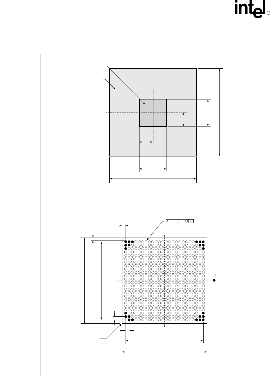
IXF1104 4-Port Gigabit Ethernet Media Access Controller
224 Datasheet
Document Number: 278757
Revision Number: 007
Revision Date: March 25, 2004
9.3 Package Information
Figure 55. CBGA Package Diagram
B0034-01
3.902
3.938
Chip
Substrate
7.804
7.877
(25 ± 0.2)
(25 ± 0.2)
47P6802
Note: All dimensions are in mm.
B0035-03
(25 ± 0.2)
(23)
(25 ± 0.2)
(23)
(23x) TYP
Chip Carrier
A01 Corner
(23x) TYP
(0.825 MAX)
(0.325 MIN)
(Reference)
(0.825 MAX)
(0.325 MIN)
(575X) (ø
0.8 ± 0.05)
(I/O Pads)
(Reference)
ø
0.20
DA
L S BS
Note: All dimensions are in mm.
= Ball
= No ball
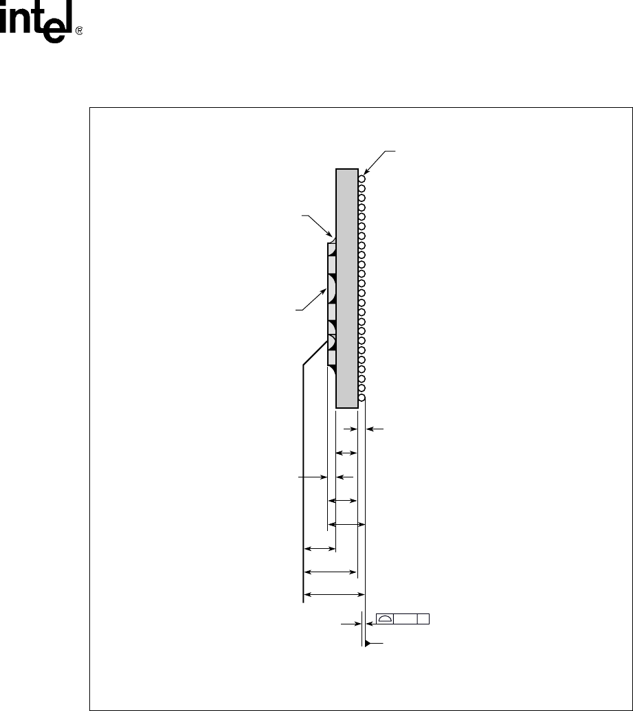
IXF1104 4-Port Gigabit Ethernet Media Access Controller
Datasheet 225
Document Number: 278757
Revision Number: 007
Revision Date: March 25, 2004
Figure 56. CBGA Package Side View Diagram
B0555-01
Seating Plane
0.15 C
(4.237 Max)
(3.619 Min)
(3.327 Max)
(2.809 Min)
(0.857 Max)
(0.779 Min)
(4.16 Max)
(3.43 Min)
(6X)
(3.24 Max)
(2.72 Min)
(6X)
(2.47 Max)
(2.03 Min)
0.81 ± 0.1
(0.77 Max)
(0.69 Min)
(6X)
Chip
C4 Encapsulant
Fillet
45L4867 (552)
Solder ball
Note: All dimensions are in mm.
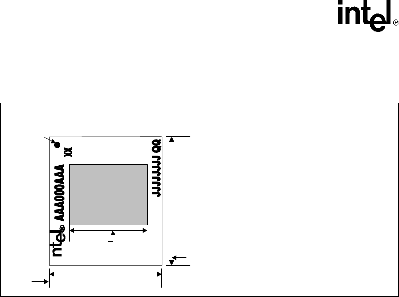
IXF1104 4-Port Gigabit Ethernet Media Access Controller
226 Datasheet
Document Number: 278757
Revision Number: 007
Revision Date: March 25, 2004
9.3.1 Example Package Marking
Figure 57. Intel® IXF1104 Example Package Marking
25.0 mm
7.5 x 7.5 mm
25.0 mm
P
in 1 mark
AAA000AAA = Intel Product Number
Country
XX = Intel Silicon revision number, A0, A1, B0 …
Substrate PN = Substrate material number (barely visible)
JJJJJJJJ = Manufacturing Lot Number
Syww9001 = Intel Finished Process Order (FPO) number
Country = Assy plant Country of Origin
Topside fields not to scale
QQ = Quality Level, P: Proto Type, PQ: Potential Qual’able,
“ ”: Production (no marking)
++
++ = Rework Indicator
Syww9001
Back of the die
(Bare Silicon)
Substrate PN
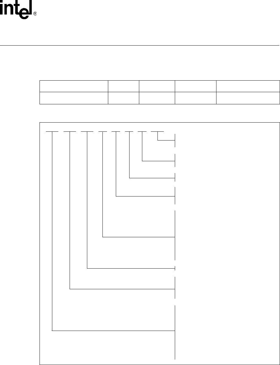
IXF1104 4-Port Gigabit Ethernet Media Access Controller
Datasheet 227
Document Number: 278757
Revision Number: 007
Revision Date: March 25, 2004
10.0 Product Ordering Information
Table 157 and Figure 58 provide IXF1104 product ordering information.
Table 157. Product Information
Number Revision Qualification MM Number Ship Media
HFIXF1104CE.B0 S 853714 B0 S 853714 Tray
Figure 58. Ordering Information – Sample
Temperature Range
A
C
E
= Ambient (0 - 55° C)
= Commercial (0 - 70° C)
= Extended (-40 - +85° C)
Product Revision
xn = 2 Alphanumeric characters
Build Format
E000
E001 = Tray
= Tape and reel
HF SB0
EC1104IXF E000
Internal Package Designator
L
P
N
Q
H
T
B
C
E
K
= LQFP
= PLCC
= DIP
= PQFP
= QFP with heat spreader
= TQFP
= BGA
= CBGA
= TBGA
= HSBGA (BGA with heat slug)
Qualification
Q
S= Pre-production material
= Production material
IXA Product Prefix
LXT
IXE
IXF
IXP
= PHY layer device
= Switching engine
= Formatting device (MAC)
= Network processor
Intel Package Designator
DJ
FA
FL
FW
HB
HD
HF
HG
S
GC
N
= LQFP
= TQFP
= PBGA (<1.0 mm pitch)
= PBGA (1.27 mm pitch)
= QFP with heat spreader
= QFP with heat slug
= CBGA
= SOIC
= QFP
= TBGA
= PLCC
xxxx = 3-5 Digit Alphanumeric Product Code
