Intel Architecture Ia 32 Users Manual Intel® Software Developer’s
IA-32 to the manual 107093aa-cf36-4768-8b52-47cec280943e
2015-02-02
: Intel Intel-Architecture-Ia-32-Users-Manual-432118 intel-architecture-ia-32-users-manual-432118 intel pdf
Open the PDF directly: View PDF ![]() .
.
Page Count: 636 [warning: Documents this large are best viewed by clicking the View PDF Link!]
- IA-32 Intel® Architecture Software Developer’s Manual
- Disclaimer
- CONTENTS FOR VOLUME 3A AND 3B
- CHAPTER 1 About This Manual
- CHAPTER 2 System Architecture Overview
- 2.1 Overview of the System-Level Architecture
- 2.2 Modes of Operation
- 2.3 System Flags and Fields in the EFLAGS Register
- 2.4 Memory-Management Registers
- 2.5 Control Registers
- 2.6 System Instruction Summary
- CHAPTER 3 Protected-Mode Memory Management
- 3.1 Memory Management Overview
- 3.2 Using Segments
- 3.3 Physical Address Space
- 3.4 Logical and Linear Addresses
- 3.5 System Descriptor Types
- 3.6 Paging (Virtual Memory) Overview
- 3.7 Page Translation using 32-Bit Physical Addressing
- 3.8 36-Bit Physical Addressing Using the PAE Paging Mechanism
- 3.8.1 Enhanced Legacy PAE Paging
- 3.8.2 Linear Address Translation With PAE Enabled (4-KByte Pages)
- 3.8.3 Linear Address Translation With PAE Enabled (2-MByte Pages)
- 3.8.4 Accessing the Full Extended Physical Address Space With the Extended Page-Table Structure
- 3.8.5 Page-Directory and Page-Table Entries With Extended Addressing Enabled
- 3.9 36-Bit Physical Addressing Using the PSE-36 Paging Mechanism
- 3.10 PAE-Enabled Paging in IA-32e Mode
- 3.11 Mapping Segments to Pages
- 3.12 Translation Lookaside Buffers (TLBs)
- CHAPTER 4 Protection
- 4.1 Enabling and Disabling Segment and Page Protection
- 4.2 Fields and Flags Used for Segment-Level and Page-Level Protection
- 4.3 Limit Checking
- 4.4 Type Checking
- 4.5 Privilege Levels
- 4.6 Privilege Level Checking When Accessing Data Segments
- 4.7 Privilege Level Checking When Loading the SS Register
- 4.8 Privilege Level Checking When Transferring Program Control Between Code Segments
- 4.8.1 Direct Calls or Jumps to Code Segments
- 4.8.2 Gate Descriptors
- 4.8.3 Call Gates
- 4.8.4 Accessing a Code Segment Through a Call Gate
- 4.8.5 Stack Switching
- 4.8.6 Returning from a Called Procedure
- 4.8.7 Performing Fast Calls to System Procedures with the SYSENTER and SYSEXIT Instructions
- 4.8.8 Fast System Calls in 64-bit Mode
- 4.9 Privileged Instructions
- 4.10 Pointer Validation
- 4.11 Page-Level Protection
- 4.12 Combining Page and Segment Protection
- 4.13 Page-Level Protection and Execute-Disable Bit
- CHAPTER 5 Interrupt and Exception Handling
- 5.1 Interrupt and Exception Overview
- 5.2 Exception and Interrupt Vectors
- 5.3 Sources of Interrupts
- 5.4 Sources of Exceptions
- 5.5 Exception Classifications
- 5.6 Program or Task Restart
- 5.7 NonMaskable Interrupt (NMI)
- 5.8 Enabling and Disabling Interrupts
- 5.9 Priority Among Simultaneous Exceptions and Interrupts
- 5.10 Interrupt Descriptor Table (IDT)
- 5.11 IDT Descriptors
- 5.12 Exception and Interrupt Handling
- 5.13 Error Code
- 5.14 Exception and Interrupt Handling in 64-bit Mode
- 5.15 Exception and Interrupt Reference
- Interrupt 0-Divide Error Exception (#DE)
- Interrupt 1-Debug Exception (#DB)
- Interrupt 2-NMI Interrupt
- Interrupt 3-Breakpoint Exception (#BP)
- Interrupt 4-Overflow Exception (#OF)
- Interrupt 5-BOUND Range Exceeded Exception (#BR)
- Interrupt 6-Invalid Opcode Exception (#UD)
- Interrupt 7-Device Not Available Exception (#NM)
- Interrupt 8-Double Fault Exception (#DF)
- Interrupt 9-Coprocessor Segment Overrun
- Interrupt 10-Invalid TSS Exception (#TS)
- Interrupt 11-Segment Not Present (#NP)
- Interrupt 12-Stack Fault Exception (#SS)
- Interrupt 13-General Protection Exception (#GP)
- Interrupt 14-Page-Fault Exception (#PF)
- Interrupt 16-x87 FPU Floating-Point Error (#MF)
- Interrupt 17-Alignment Check Exception (#AC)
- Interrupt 18-Machine-Check Exception (#MC)
- Interrupt 19-SIMD Floating-Point Exception (#XF)
- Interrupts 32 to 255-User Defined Interrupts
- CHAPTER 6 Task Management
- CHAPTER 7 Multiple-Processor Management
- 7.1 Locked Atomic Operations
- 7.2 Memory Ordering
- 7.3 Propagation of Page Table and Page Directory Entry Changes to Multiple Processors
- 7.4 Serializing Instructions
- 7.5 Multiple-Processor (MP) Initialization
- 7.6 Hyper-Threading and Multi-Core Technology
- 7.7 Detecting Hardware Multi-Threading Support and Topology
- 7.8 Intel® Hyper-Threading Technology Architecture
- 7.8.1 State of the Logical Processors
- 7.8.2 APIC Functionality
- 7.8.3 Memory Type Range Registers (MTRR)
- 7.8.4 Page Attribute Table (PAT)
- 7.8.5 Machine Check Architecture
- 7.8.6 Debug Registers and Extensions
- 7.8.7 Performance Monitoring Counters
- 7.8.8 IA32_MISC_ENABLE MSR
- 7.8.9 Memory Ordering
- 7.8.10 Serializing Instructions
- 7.8.11 MICROCODE UPDATE Resources
- 7.8.12 Self Modifying Code
- 7.8.13 Implementation-Specific HT Technology Facilities
- 7.9 Dual-Core Architecture
- 7.10 Programming Considerations for Hardware Multi-Threading Capable Processors
- 7.11 Management of Idle and Blocked Conditions
- 7.11.1 HLT Instruction
- 7.11.2 PAUSE Instruction
- 7.11.3 Detecting Support MONITOR/MWAIT Instruction
- 7.11.4 MONITOR/MWAIT Instruction
- 7.11.5 Monitor/Mwait Address Range Determination
- 7.11.6 Required Operating System Support
- 7.11.6.1 Use the PAUSE Instruction in Spin-Wait Loops
- 7.11.6.2 Potential Usage of MONITOR/MWAIT in C0 Idle Loops
- 7.11.6.3 Halt Idle Logical Processors
- 7.11.6.4 Potential Usage of MONITOR/MWAIT in C1 Idle Loops
- 7.11.6.5 Guidelines for Scheduling Threads on Logical Processors Sharing Execution Resources
- 7.11.6.6 Eliminate Execution-Based Timing Loops
- 7.11.6.7 Place Locks and Semaphores in Aligned, 128-Byte Blocks of Memory
- CHAPTER 8 Advanced Programmable Interrupt Controller (APIC)
- 8.1 Local and I/O APIC Overview
- 8.2 System Bus Vs. APIC Bus
- 8.3 the Intel® 82489DX External APIC, The APIC, and the xAPIC
- 8.4 Local APIC
- 8.5 Handling Local Interrupts
- 8.6 Issuing Interprocessor Interrupts
- 8.7 System and APIC Bus Arbitration
- 8.8 Handling Interrupts
- 8.8.1 Interrupt Handling with the Pentium 4 and Intel Xeon Processors
- 8.8.2 Interrupt Handling with the P6 Family and Pentium Processors
- 8.8.3 Interrupt, Task, and Processor Priority
- 8.8.4 Interrupt Acceptance for Fixed Interrupts
- 8.8.5 Signaling Interrupt Servicing Completion
- 8.8.6 Task Priority in IA-32e Mode
- 8.9 Spurious Interrupt
- 8.10 APIC Bus Message Passing Mechanism and Protocol (P6 Family, Pentium Processors)
- 8.11 Message Signalled Interrupts
- CHAPTER 9 Processor Management and Initialization
- 9.1 Initialization Overview
- 9.2 x87 FPU Initialization
- 9.3 Cache Enabling
- 9.4 Model-Specific Registers (MSRs)
- 9.5 Memory Type Range Registers (MTRRs)
- 9.6 Initializing SSE/SSE2/SSE3 Extensions
- 9.7 Software Initialization for Real-Address Mode Operation
- 9.8 Software Initialization for Protected-Mode Operation
- 9.9 Mode Switching
- 9.10 Initialization and Mode Switching Example
- 9.11 Microcode Update Facilities
- 9.11.1 Microcode Update
- 9.11.2 Optional Extended Signature Table
- 9.11.3 Processor Identification
- 9.11.4 Platform Identification
- 9.11.5 Microcode Update Checksum
- 9.11.6 Microcode Update Loader
- 9.11.7 Update Signature and Verification
- 9.11.8 Pentium 4, Intel Xeon, and P6 Family Processor Microcode Update Specifications
- 9.11.8.1 Responsibilities of the BIOS
- 9.11.8.2 Responsibilities of the Calling Program
- 9.11.8.3 Microcode Update Functions
- 9.11.8.4 INT 15H-based Interface
- 9.11.8.5 Function 00H-Presence Test
- 9.11.8.6 Function 01H-Write Microcode Update Data
- 9.11.8.7 Function 02H-Microcode Update Control
- 9.11.8.8 Function 03H-Read Microcode Update Data
- 9.11.8.9 Return Codes
- CHAPTER 10 Memory Cache Control
- 10.1 Internal Caches, TLBs, and Buffers
- 10.2 Caching Terminology
- 10.3 Methods of Caching Available
- 10.4 Cache Control Protocol
- 10.5 Cache Control
- 10.6 Self-Modifying Code
- 10.7 Implicit Caching (Pentium 4, Intel Xeon, and P6 Family Processors)
- 10.8 Explicit Caching
- 10.9 Invalidating the Translation Lookaside Buffers (TLBs)
- 10.10 Store Buffer
- 10.11 Memory Type Range Registers (MTRRs)
- 10.11.1 MTRR Feature Identification
- 10.11.2 Setting Memory Ranges with MTRRs
- 10.11.3 Example Base and Mask Calculations
- 10.11.4 Range Size and Alignment Requirement
- 10.11.5 MTRR Initialization
- 10.11.6 Remapping Memory Types
- 10.11.7 MTRR Maintenance Programming Interface
- 10.11.8 MTRR Considerations in MP Systems
- 10.11.9 Large Page Size Considerations
- 10.12 Page Attribute Table (PAT)
- CHAPTER 11 Intel® MMX™ Technology System Programming
- CHAPTER 12 SSE, SSE2 and SSE3 System Programming
- 12.1 Providing Operating System Support for SSE/SSE2/SSE3 Extensions
- 12.1.1 Adding Support to an Operating System for SSE/SSE2/SSE3 Extensions
- 12.1.2 Checking for SSE/SSE2/SSE3 Extension Support
- 12.1.3 Checking for Support for the FXSAVE and FXRSTOR Instructions
- 12.1.4 Initialization of the SSE/SSE2/SSE3 Extensions
- 12.1.5 Providing Non-Numeric Exception Handlers for Exceptions Generated by the SSE/SSE2/SSE3 Instructions
- 12.1.6 Providing an Handler for the SIMD Floating-Point Exception (#XF)
- 12.2 Emulation of SSE/SSE2/SSE3 Extensions
- 12.3 Saving and Restoring the SSE/SSE2/SSE3 State
- 12.4 Saving the SSE/SSE2/SSE3 State on Task or Context Switches
- 12.5 Designing OS Facilities for AUTOMATICALLY Saving x87 FPU, MMX, and SSE/SSE2/SSE3 state on Task or Context Switches
- 12.1 Providing Operating System Support for SSE/SSE2/SSE3 Extensions
- CHAPTER 13 Power and Thermal Management
- 13.1 Enhanced Intel Speedstep® Technology
- 13.2 P-State Hardware Coordination
- 13.3 MWAIT Extensions for Advanced Power Management
- 13.4 Thermal Monitoring and Protection
- CHAPTER 14 Machine-Check Architecture
- 14.1 Machine-Check Exceptions and Architecture
- 14.2 Compatibility with Pentium Processor
- 14.3 Machine-Check MSRs
- 14.4 Machine-Check Availability
- 14.5 Machine-Check Initialization
- 14.6. Interpreting the MCA Error Codes
- 14.7 Guidelines for Writing Machine-Check Software
- CHAPTER 15 8086 Emulation
- 15.1 Real-Address Mode
- 15.2 Virtual-8086 Mode
- 15.3 Interrupt and Exception Handling in Virtual-8086 Mode
- 15.4 Protected-Mode Virtual Interrupts
- CHAPTER 16 Mixing 16-Bit and 32-Bit Code
- CHAPTER 17 IA-32 Architecture Compatibility
- 17.1. IA-32 Processor Families and Categories
- 17.2. Reserved Bits
- 17.3. Enabling New Functions and Modes
- 17.4. Detecting the Presence of New Features Through Software
- 17.5. Intel MMX Technology
- 17.6. Streaming SIMD Extensions (SSE)
- 17.7. Streaming SIMD Extensions 2 (SSE2)
- 17.8. Streaming SIMD Extensions 3 (SSE3)
- 17.9. Hyper-Threading Technology
- 17.10. Dual-Core Technology
- 17.11. Specific Features of Dual-Core Processor
- 17.12. New Instructions In the Pentium and Later IA-32 Processors
- 17.13. Obsolete Instructions
- 17.14. Undefined Opcodes
- 17.15. New Flags in the EFLAGS Register
- 17.16. Stack Operations
- 17.17. x87 FPU
- 17.17.1 Control Register CR0 Flags
- 17.17.2 x87 FPU Status Word
- 17.17.3 x87 FPU Control Word
- 17.17.4 x87 FPU Tag Word
- 17.17.5 Data Types
- 17.17.6 Floating-Point Exceptions
- 17.17.6.1 Denormal Operand Exception (#D)
- 17.17.6.2 Numeric Overflow Exception (#O)
- 17.17.6.3 Numeric Underflow Exception (#U)
- 17.17.6.4 Exception Precedence
- 17.17.6.5 CS and EIP For FPU Exceptions
- 17.17.6.6 FPU Error Signals
- 17.17.6.7 Assertion of the FERR# Pin
- 17.17.6.8 Invalid Operation Exception On Denormals
- 17.17.6.9 Alignment Check Exceptions (#AC)
- 17.17.6.10 Segment Not Present Exception During FLDENV
- 17.17.6.11 Device Not Available Exception (#NM)
- 17.17.6.12 Coprocessor Segment Overrun Exception
- 17.17.6.13 General Protection Exception (#GP)
- 17.17.6.14 Floating-Point Error Exception (#MF)
- 17.17.7 Changes to Floating-Point Instructions
- 17.17.7.1 FDIV, FPREM, and FSQRT Instructions
- 17.17.7.2 FSCALE Instruction
- 17.17.7.3 FPREM1 Instruction
- 17.17.7.4 FPREM Instruction
- 17.17.7.5 FUCOM, FUCOMP, and FUCOMPP Instructions
- 17.17.7.6 FPTAN Instruction
- 17.17.7.7 Stack Overflow
- 17.17.7.8 FSIN, FCOS, and FSINCOS Instructions
- 17.17.7.9 FPATAN Instruction
- 17.17.7.10 F2XM1 Instruction
- 17.17.7.11 FLD Instruction
- 17.17.7.12 FXTRACT Instruction
- 17.17.7.13 Load Constant Instructions
- 17.17.7.14 FSETPM Instruction
- 17.17.7.15 FXAM Instruction
- 17.17.7.16 FSAVE and FSTENV Instructions
- 17.17.8 Transcendental Instructions
- 17.17.9 Obsolete Instructions
- 17.17.10 WAIT/FWAIT Prefix Differences
- 17.17.11 Operands Split Across Segments and/or Pages
- 17.17.12 FPU Instruction Synchronization
- 17.18. Serializing Instructions
- 17.19. FPU and Math Coprocessor Initialization
- 17.20. Control Registers
- 17.21. Memory Management Facilities
- 17.22. Debug Facilities
- 17.23. Recognition of Breakpoints
- 17.24. Exceptions and/or Exception Conditions
- 17.25. Interrupts
- 17.26. Advanced Programmable Interrupt Controller (APIC)
- 17.27. Task Switching and TSs
- 17.28. Cache Management
- 17.29. Paging
- 17.30. Stack Operations
- 17.31. Mixing 16- and 32-Bit Segments
- 17.32. Segment and Address Wraparound
- 17.33. Store Buffers and Memory Ordering
- 17.34. Bus Locking
- 17.35. Bus Hold
- 17.36. Model-Specific Extensions to the IA-32
- 17.37. Two Ways to Run Intel 286 Processor Tasks

IA-32 Intel® Architecture
Software Developer’s Manual
Volume 3A:
System Programming Guide, Part 1
NOTE: The IA-32 Intel Architecture Software Developer's Manual consists
of five volumes: Basic Architecture, Order Number 253665; Instruction
Set Reference A-M, Order Number 253666; Instruction Set Reference N-Z,
Order Number 253667; System Programming Guide, Part 1, Order
Number 253668; System Programming Guide, Part 2, Order Number
253669. Refer to all five volumes when evaluating your design needs.
Order Number: 253668-019
March 2006

INFORMATION IN THIS DOCUMENT IS PROVIDED IN CONNECTION WITH INTEL PRODUCTS. NO LICENSE, EX-
PRESS OR IMPLIED, BY ESTOPPEL OR OTHERWISE, TO ANY INTELLECTUAL PROPERTY RIGHTS IS GRANTED BY
THIS DOCUMENT. EXCEPT AS PROVIDED IN INTEL’S TERMS AND CONDITIONS OF SALE FOR SUCH PRODUCTS,
INTEL ASSUMES NO LIABILITY WHATSOEVER, AND INTEL DISCLAIMS ANY EXPRESS OR IMPLIED WARRANTY, RE-
LATING TO SALE AND/OR USE OF INTEL PRODUCTS INCLUDING LIABILITY OR WARRANTIES RELATING TO FIT-
NESS FOR A PARTICULAR PURPOSE, MERCHANTABILITY, OR INFRINGEMENT OF ANY PATENT, COPYRIGHT OR
OTHER INTELLECTUAL PROPERTY RIGHT. INTEL PRODUCTS ARE NOT INTENDED FOR USE IN MEDICAL, LIFE
SAVING, OR LIFE SUSTAINING APPLICATIONS.
Intel may make changes to specifications and product descriptions at any time, without notice.
Developers must not rely on the absence or characteristics of any features or instructions marked “reserved” or “undefined.”
Improper use of reserved or undefined features or instructions may cause unpredictable behavior or failure in developer's
software code when running on an Intel processor. Intel reserves these features or instructions for future definition and shall
have no responsibility whatsoever for conflicts or incompatibilities arising from their unauthorized use.
The Intel® IA-32 architecture processors (e.g., Pentium® 4 and Pentium III processors) may contain design defects or errors
known as errata. Current characterized errata are available on request.
Hyper-Threading Technology requires a computer system with an Intel® Pentium® 4 processor supporting Hyper-Threading
Technology and an HT Technology enabled chipset, BIOS and operating system. Performance will vary depending on the
specific hardware and software you use. See http://www.intel.com/techtrends/technologies/hyperthreading.htm for more in-
formation including details on which processors support HT Technology.
Intel® Virtualization Technology requires a computer system with an enabled Intel® processor, BIOS, virtual machine monitor
(VMM) and for some uses, certain platform software enabled for it. Functionality, performance or other benefits will vary de-
pending on hardware and software configurations. Intel® Virtualization Technology-enabled BIOS and VMM applications are
currently in development.
Intel® Extended Memory 64 Technology (Intel® EM64T) requires a computer system with a processor, chipset, BIOS, OS,
device drivers and applications enabled for Intel EM64T. Processor will not operate (including 32-bit operation) with-
out an Intel EM64T-enabled BIOS. Performance will vary depending on your hardware and software configurations. Intel
EM64T-enabled OS, BIOS, device drivers and applications may not be available. Check with your vendor for more
information.
Intel, Pentium, Intel Xeon, Intel NetBurst, Intel Core Solo, Intel Core Duo, Intel Pentium D, Itanium, MMX, and VTune are
trademarks or registered trademarks of Intel Corporation or its subsidiaries in the United States and other countries.
*Other names and brands may be claimed as the property of others.
Contact your local Intel sales office or your distributor to obtain the latest specifications and before placing your product order.
Copies of documents which have an ordering number and are referenced in this document, or other Intel literature, may be
obtained from:
Intel Corporation
P.O. Box 5937
Denver, CO 80217-9808
or call 1-800-548-4725
or visit Intel’s website at http://www.intel.com
Copyright © 1997-2006 Intel Corporation

Vol. 3A iii
CONTENTS FOR VOLUME 3A AND 3B
CHAPTER 1
ABOUT THIS MANUAL
1.1 IA-32 PROCESSORS COVERED IN THIS MANUAL . . . . . . . . . . . . . . . . . . . . . . . 1-1
1.2 OVERVIEW OF THE SYSTEM PROGRAMMING GUIDE. . . . . . . . . . . . . . . . . . . . 1-2
1.3 NOTATIONAL CONVENTIONS. . . . . . . . . . . . . . . . . . . . . . . . . . . . . . . . . . . . . . . . 1-4
1.3.1 Bit and Byte Order. . . . . . . . . . . . . . . . . . . . . . . . . . . . . . . . . . . . . . . . . . . . . . . . .1-5
1.3.2 Reserved Bits and Software Compatibility . . . . . . . . . . . . . . . . . . . . . . . . . . . . . .1-5
1.3.3 Instruction Operands . . . . . . . . . . . . . . . . . . . . . . . . . . . . . . . . . . . . . . . . . . . . . . .1-6
1.3.4 Hexadecimal and Binary Numbers . . . . . . . . . . . . . . . . . . . . . . . . . . . . . . . . . . . .1-7
1.3.5 Segmented Addressing . . . . . . . . . . . . . . . . . . . . . . . . . . . . . . . . . . . . . . . . . . . . .1-7
1.3.6 Syntax for CPUID, CR, and MSR Values . . . . . . . . . . . . . . . . . . . . . . . . . . . . . . .1-7
1.3.7 Exceptions. . . . . . . . . . . . . . . . . . . . . . . . . . . . . . . . . . . . . . . . . . . . . . . . . . . . . . .1-8
1.4 RELATED LITERATURE . . . . . . . . . . . . . . . . . . . . . . . . . . . . . . . . . . . . . . . . . . . . . 1-9
CHAPTER 2
SYSTEM ARCHITECTURE OVERVIEW
2.1 OVERVIEW OF THE SYSTEM-LEVEL ARCHITECTURE . . . . . . . . . . . . . . . . . . . 2-2
2.1.1 Global and Local Descriptor Tables . . . . . . . . . . . . . . . . . . . . . . . . . . . . . . . . . . .2-5
2.1.1.1 Global and Local Descriptor Tables in IA-32 Mode . . . . . . . . . . . . . . . . . . . . .2-5
2.1.2 System Segments, Segment Descriptors, and Gates . . . . . . . . . . . . . . . . . . . . . .2-5
2.1.2.1 Gates in IA-32e Mode. . . . . . . . . . . . . . . . . . . . . . . . . . . . . . . . . . . . . . . . . . . .2-6
2.1.3 Task-State Segments and Task Gates . . . . . . . . . . . . . . . . . . . . . . . . . . . . . . . . .2-6
2.1.3.1 Task-State Segments in IA-32e Mode . . . . . . . . . . . . . . . . . . . . . . . . . . . . . . .2-7
2.1.4 Interrupt and Exception Handling . . . . . . . . . . . . . . . . . . . . . . . . . . . . . . . . . . . . .2-7
2.1.4.1 Interrupt and Exception Handling IA-32e Mode . . . . . . . . . . . . . . . . . . . . . . . .2-7
2.1.5 Memory Management . . . . . . . . . . . . . . . . . . . . . . . . . . . . . . . . . . . . . . . . . . . . . .2-7
2.1.5.1 Memory Management in IA-32e Mode . . . . . . . . . . . . . . . . . . . . . . . . . . . . . .2-8
2.1.6 System Registers . . . . . . . . . . . . . . . . . . . . . . . . . . . . . . . . . . . . . . . . . . . . . . . . .2-8
2.1.6.1 System Registers in IA-32e Mode . . . . . . . . . . . . . . . . . . . . . . . . . . . . . . . . . .2-9
2.1.7 Other System Resources . . . . . . . . . . . . . . . . . . . . . . . . . . . . . . . . . . . . . . . . . .2-10
2.2 MODES OF OPERATION . . . . . . . . . . . . . . . . . . . . . . . . . . . . . . . . . . . . . . . . . . . 2-10
2.3 SYSTEM FLAGS AND FIELDS IN THE EFLAGS REGISTER . . . . . . . . . . . . . . . 2-12
2.3.1 System Flags and Fields in IA-32e Mode . . . . . . . . . . . . . . . . . . . . . . . . . . . . . .2-14
2.4 MEMORY-MANAGEMENT REGISTERS . . . . . . . . . . . . . . . . . . . . . . . . . . . . . . . 2-14
2.4.1 Global Descriptor Table Register (GDTR). . . . . . . . . . . . . . . . . . . . . . . . . . . . . .2-15
2.4.2 Local Descriptor Table Register (LDTR) . . . . . . . . . . . . . . . . . . . . . . . . . . . . . . .2-15
2.4.3 IDTR Interrupt Descriptor Table Register . . . . . . . . . . . . . . . . . . . . . . . . . . . . . .2-16
2.4.4 Task Register (TR) . . . . . . . . . . . . . . . . . . . . . . . . . . . . . . . . . . . . . . . . . . . . . . .2-16
2.5 CONTROL REGISTERS . . . . . . . . . . . . . . . . . . . . . . . . . . . . . . . . . . . . . . . . . . . . 2-16
2.5.1 CPUID Qualification of Control Register Flags . . . . . . . . . . . . . . . . . . . . . . . . . .2-24
2.6 SYSTEM INSTRUCTION SUMMARY . . . . . . . . . . . . . . . . . . . . . . . . . . . . . . . . . . 2-24
2.6.1 Loading and Storing System Registers. . . . . . . . . . . . . . . . . . . . . . . . . . . . . . . .2-25
2.6.2 Verifying of Access Privileges . . . . . . . . . . . . . . . . . . . . . . . . . . . . . . . . . . . . . . .2-26
2.6.3 Loading and Storing Debug Registers. . . . . . . . . . . . . . . . . . . . . . . . . . . . . . . . .2-27
2.6.4 Invalidating Caches and TLBs. . . . . . . . . . . . . . . . . . . . . . . . . . . . . . . . . . . . . . .2-27
2.6.5 Controlling the Processor . . . . . . . . . . . . . . . . . . . . . . . . . . . . . . . . . . . . . . . . . .2-27
2.6.6 Reading Performance-Monitoring and Time-Stamp Counters . . . . . . . . . . . . . .2-28
2.6.6.1 Reading Counters in 64-Bit Mode. . . . . . . . . . . . . . . . . . . . . . . . . . . . . . . . . .2-29

CONTENTS
iv Vol. 3A
PAGE
2.6.7 Reading and Writing Model-Specific Registers . . . . . . . . . . . . . . . . . . . . . . . . . .2-29
2.6.7.1 Reading and Writing Model-Specific Registers in 64-Bit Mode . . . . . . . . . . .2-29
CHAPTER 3
PROTECTED-MODE MEMORY MANAGEMENT
3.1 MEMORY MANAGEMENT OVERVIEW . . . . . . . . . . . . . . . . . . . . . . . . . . . . . . . . . 3-1
3.2 USING SEGMENTS. . . . . . . . . . . . . . . . . . . . . . . . . . . . . . . . . . . . . . . . . . . . . . . . . 3-3
3.2.1 Basic Flat Model . . . . . . . . . . . . . . . . . . . . . . . . . . . . . . . . . . . . . . . . . . . . . . . . . .3-3
3.2.2 Protected Flat Model . . . . . . . . . . . . . . . . . . . . . . . . . . . . . . . . . . . . . . . . . . . . . . .3-3
3.2.3 Multi-Segment Model. . . . . . . . . . . . . . . . . . . . . . . . . . . . . . . . . . . . . . . . . . . . . . .3-5
3.2.4 Segmentation in IA-32e Mode. . . . . . . . . . . . . . . . . . . . . . . . . . . . . . . . . . . . . . . .3-6
3.2.5 Paging and Segmentation . . . . . . . . . . . . . . . . . . . . . . . . . . . . . . . . . . . . . . . . . . .3-6
3.3 PHYSICAL ADDRESS SPACE . . . . . . . . . . . . . . . . . . . . . . . . . . . . . . . . . . . . . . . . 3-6
3.3.1 Physical Address Space for Processors with Intel® EM64T . . . . . . . . . . . . . . . . .3-7
3.4 LOGICAL AND LINEAR ADDRESSES . . . . . . . . . . . . . . . . . . . . . . . . . . . . . . . . . . 3-7
3.4.1 Logical Address Translation in IA-32e Mode. . . . . . . . . . . . . . . . . . . . . . . . . . . . .3-8
3.4.2 Segment Selectors . . . . . . . . . . . . . . . . . . . . . . . . . . . . . . . . . . . . . . . . . . . . . . . .3-8
3.4.3 Segment Registers . . . . . . . . . . . . . . . . . . . . . . . . . . . . . . . . . . . . . . . . . . . . . . . .3-9
3.4.4 Segment Loading Instructions in IA-32e Mode . . . . . . . . . . . . . . . . . . . . . . . . . .3-11
3.4.5 Segment Descriptors. . . . . . . . . . . . . . . . . . . . . . . . . . . . . . . . . . . . . . . . . . . . . .3-12
3.4.5.1 Code- and Data-Segment Descriptor Types. . . . . . . . . . . . . . . . . . . . . . . . . .3-15
3.5 SYSTEM DESCRIPTOR TYPES . . . . . . . . . . . . . . . . . . . . . . . . . . . . . . . . . . . . . . 3-17
3.5.1 Segment Descriptor Tables. . . . . . . . . . . . . . . . . . . . . . . . . . . . . . . . . . . . . . . . .3-18
3.5.2 Segment Descriptor Tables in IA-32e Mode . . . . . . . . . . . . . . . . . . . . . . . . . . . .3-20
3.6 PAGING (VIRTUAL MEMORY) OVERVIEW . . . . . . . . . . . . . . . . . . . . . . . . . . . . . 3-20
3.6.1 Paging Options . . . . . . . . . . . . . . . . . . . . . . . . . . . . . . . . . . . . . . . . . . . . . . . . . .3-21
3.6.2 Page Tables and Directories in the Absence of Intel EM64T . . . . . . . . . . . . . . .3-22
3.7 PAGE TRANSLATION USING 32-BIT PHYSICAL ADDRESSING . . . . . . . . . . . . 3-22
3.7.1 Linear Address Translation (4-KByte Pages) . . . . . . . . . . . . . . . . . . . . . . . . . . .3-23
3.7.2 Linear Address Translation (4-MByte Pages) . . . . . . . . . . . . . . . . . . . . . . . . . . .3-24
3.7.3 Mixing 4-KByte and 4-MByte Pages . . . . . . . . . . . . . . . . . . . . . . . . . . . . . . . . . .3-25
3.7.4 Memory Aliasing . . . . . . . . . . . . . . . . . . . . . . . . . . . . . . . . . . . . . . . . . . . . . . . . .3-25
3.7.5 Base Address of the Page Directory . . . . . . . . . . . . . . . . . . . . . . . . . . . . . . . . . .3-25
3.7.6 Page-Directory and Page-Table Entries . . . . . . . . . . . . . . . . . . . . . . . . . . . . . . .3-26
3.7.7 Not Present Page-Directory and Page-Table Entries . . . . . . . . . . . . . . . . . . . . .3-30
3.8 36-BIT PHYSICAL ADDRESSING USING THE PAE PAGING MECHANISM . . . 3-30
3.8.1 Enhanced Legacy PAE Paging . . . . . . . . . . . . . . . . . . . . . . . . . . . . . . . . . . . . . .3-31
3.8.2 Linear Address Translation With PAE Enabled (4-KByte Pages) . . . . . . . . . . . .3-31
3.8.3 Linear Address Translation With PAE Enabled (2-MByte Pages). . . . . . . . . . . .3-32
3.8.4 Accessing the Full Extended Physical Address Space With the
Extended Page-Table Structure . . . . . . . . . . . . . . . . . . . . . . . . . . . . . . . . . . . . .3-33
3.8.5 Page-Directory and Page-Table Entries With Extended Addressing
Enabled . . . . . . . . . . . . . . . . . . . . . . . . . . . . . . . . . . . . . . . . . . . . . . . . . . . . . . . .3-34
3.9 36-BIT PHYSICAL ADDRESSING USING THE PSE-36 PAGING
MECHANISM . . . . . . . . . . . . . . . . . . . . . . . . . . . . . . . . . . . . . . . . . . . . . . . . . . . . . 3-37
3.10 PAE-ENABLED PAGING IN IA-32E MODE. . . . . . . . . . . . . . . . . . . . . . . . . . . . . . 3-39
3.10.1 IA-32e Mode Linear Address Translation (4-KByte Pages). . . . . . . . . . . . . . . . .3-39
3.10.2 IA-32e Mode Linear Address Translation (2-MByte Pages) . . . . . . . . . . . . . . . .3-40
3.10.3 Enhanced Paging Data Structures . . . . . . . . . . . . . . . . . . . . . . . . . . . . . . . . . . .3-41
3.10.3.1 Reserved Bit Checking . . . . . . . . . . . . . . . . . . . . . . . . . . . . . . . . . . . . . . . . . .3-43
3.11 MAPPING SEGMENTS TO PAGES . . . . . . . . . . . . . . . . . . . . . . . . . . . . . . . . . . . 3-45
3.12 TRANSLATION LOOKASIDE BUFFERS (TLBS) . . . . . . . . . . . . . . . . . . . . . . . . . 3-46

Vol. 3A v
CONTENTS
PAGE
CHAPTER 4
PROTECTION
4.1 ENABLING AND DISABLING SEGMENT AND PAGE PROTECTION . . . . . . . . . . 4-1
4.2 FIELDS AND FLAGS USED FOR SEGMENT-LEVEL AND
PAGE-LEVEL PROTECTION. . . . . . . . . . . . . . . . . . . . . . . . . . . . . . . . . . . . . . . . . . 4-2
4.2.1 Code Segment Descriptor in 64-bit Mode . . . . . . . . . . . . . . . . . . . . . . . . . . . . . . 4-4
4.3 LIMIT CHECKING . . . . . . . . . . . . . . . . . . . . . . . . . . . . . . . . . . . . . . . . . . . . . . . . . . 4-5
4.3.1 Limit Checking in 64-bit Mode . . . . . . . . . . . . . . . . . . . . . . . . . . . . . . . . . . . . . . . 4-6
4.4 TYPE CHECKING . . . . . . . . . . . . . . . . . . . . . . . . . . . . . . . . . . . . . . . . . . . . . . . . . . 4-6
4.4.1 Null Segment Selector Checking. . . . . . . . . . . . . . . . . . . . . . . . . . . . . . . . . . . . . 4-8
4.4.1.1 NULL Segment Checking in 64-bit Mode . . . . . . . . . . . . . . . . . . . . . . . . . . . . 4-8
4.5 PRIVILEGE LEVELS . . . . . . . . . . . . . . . . . . . . . . . . . . . . . . . . . . . . . . . . . . . . . . . . 4-8
4.6 PRIVILEGE LEVEL CHECKING WHEN ACCESSING DATA SEGMENTS. . . . . . 4-11
4.6.1 Accessing Data in Code Segments . . . . . . . . . . . . . . . . . . . . . . . . . . . . . . . . . . 4-13
4.7 PRIVILEGE LEVEL CHECKING WHEN LOADING THE SS REGISTER . . . . . . . 4-13
4.8 PRIVILEGE LEVEL CHECKING WHEN TRANSFERRING PROGRAM
CONTROL BETWEEN CODE SEGMENTS. . . . . . . . . . . . . . . . . . . . . . . . . . . . . . 4-13
4.8.1 Direct Calls or Jumps to Code Segments . . . . . . . . . . . . . . . . . . . . . . . . . . . . . 4-14
4.8.1.1 Accessing Nonconforming Code Segments . . . . . . . . . . . . . . . . . . . . . . . . . 4-15
4.8.1.2 Accessing Conforming Code Segments . . . . . . . . . . . . . . . . . . . . . . . . . . . . 4-16
4.8.2 Gate Descriptors . . . . . . . . . . . . . . . . . . . . . . . . . . . . . . . . . . . . . . . . . . . . . . . . 4-17
4.8.3 Call Gates . . . . . . . . . . . . . . . . . . . . . . . . . . . . . . . . . . . . . . . . . . . . . . . . . . . . . 4-18
4.8.3.1 IA-32e Mode Call Gates . . . . . . . . . . . . . . . . . . . . . . . . . . . . . . . . . . . . . . . . 4-19
4.8.4 Accessing a Code Segment Through a Call Gate. . . . . . . . . . . . . . . . . . . . . . . 4-20
4.8.5 Stack Switching . . . . . . . . . . . . . . . . . . . . . . . . . . . . . . . . . . . . . . . . . . . . . . . . . 4-23
4.8.5.1 Stack Switching in 64-bit Mode. . . . . . . . . . . . . . . . . . . . . . . . . . . . . . . . . . . 4-26
4.8.6 Returning from a Called Procedure . . . . . . . . . . . . . . . . . . . . . . . . . . . . . . . . . . 4-26
4.8.7 Performing Fast Calls to System Procedures with the
SYSENTER and SYSEXIT Instructions. . . . . . . . . . . . . . . . . . . . . . . . . . . . . . . 4-28
4.8.7.1 SYSENTER and SYSEXIT Instructions in IA-32e Mode. . . . . . . . . . . . . . . . 4-29
4.8.8 Fast System Calls in 64-bit Mode . . . . . . . . . . . . . . . . . . . . . . . . . . . . . . . . . . . 4-30
4.9 PRIVILEGED INSTRUCTIONS . . . . . . . . . . . . . . . . . . . . . . . . . . . . . . . . . . . . . . . 4-32
4.10 POINTER VALIDATION . . . . . . . . . . . . . . . . . . . . . . . . . . . . . . . . . . . . . . . . . . . . . 4-32
4.10.1 Checking Access Rights (LAR Instruction) . . . . . . . . . . . . . . . . . . . . . . . . . . . . 4-33
4.10.2 Checking Read/Write Rights (VERR and VERW Instructions) . . . . . . . . . . . . . 4-34
4.10.3 Checking That the Pointer Offset Is Within Limits (LSL Instruction) . . . . . . . . . 4-34
4.10.4 Checking Caller Access Privileges (ARPL Instruction) . . . . . . . . . . . . . . . . . . . 4-35
4.10.5 Checking Alignment. . . . . . . . . . . . . . . . . . . . . . . . . . . . . . . . . . . . . . . . . . . . . . 4-37
4.11 PAGE-LEVEL PROTECTION. . . . . . . . . . . . . . . . . . . . . . . . . . . . . . . . . . . . . . . . . 4-37
4.11.1 Page-Protection Flags . . . . . . . . . . . . . . . . . . . . . . . . . . . . . . . . . . . . . . . . . . . . 4-38
4.11.2 Restricting Addressable Domain . . . . . . . . . . . . . . . . . . . . . . . . . . . . . . . . . . . . 4-38
4.11.3 Page Type . . . . . . . . . . . . . . . . . . . . . . . . . . . . . . . . . . . . . . . . . . . . . . . . . . . . . 4-38
4.11.4 Combining Protection of Both Levels of Page Tables . . . . . . . . . . . . . . . . . . . . 4-39
4.11.5 Overrides to Page Protection. . . . . . . . . . . . . . . . . . . . . . . . . . . . . . . . . . . . . . . 4-39
4.12 COMBINING PAGE AND SEGMENT PROTECTION . . . . . . . . . . . . . . . . . . . . . . 4-39
4.13 PAGE-LEVEL PROTECTION AND EXECUTE-DISABLE BIT. . . . . . . . . . . . . . . . 4-40
4.13.1 Detecting and Enabling the Execute-Disable Bit Capability. . . . . . . . . . . . . . . . 4-41
4.13.2 Execute-Disable Bit Page Protection. . . . . . . . . . . . . . . . . . . . . . . . . . . . . . . . . 4-41
4.13.3 Reserved Bit Checking . . . . . . . . . . . . . . . . . . . . . . . . . . . . . . . . . . . . . . . . . . . 4-43
4.13.4 Exception Handling . . . . . . . . . . . . . . . . . . . . . . . . . . . . . . . . . . . . . . . . . . . . . . 4-44

CONTENTS
vi Vol. 3A
PAGE
CHAPTER 5
INTERRUPT AND EXCEPTION HANDLING
5.1 INTERRUPT AND EXCEPTION OVERVIEW . . . . . . . . . . . . . . . . . . . . . . . . . . . . . 5-1
5.2 EXCEPTION AND INTERRUPT VECTORS . . . . . . . . . . . . . . . . . . . . . . . . . . . . . . 5-2
5.3 SOURCES OF INTERRUPTS . . . . . . . . . . . . . . . . . . . . . . . . . . . . . . . . . . . . . . . . . 5-2
5.3.1 External Interrupts. . . . . . . . . . . . . . . . . . . . . . . . . . . . . . . . . . . . . . . . . . . . . . . . .5-2
5.3.2 Maskable Hardware Interrupts . . . . . . . . . . . . . . . . . . . . . . . . . . . . . . . . . . . . . . .5-4
5.3.3 Software-Generated Interrupts . . . . . . . . . . . . . . . . . . . . . . . . . . . . . . . . . . . . . . .5-4
5.4 SOURCES OF EXCEPTIONS . . . . . . . . . . . . . . . . . . . . . . . . . . . . . . . . . . . . . . . . . 5-5
5.4.1 Program-Error Exceptions. . . . . . . . . . . . . . . . . . . . . . . . . . . . . . . . . . . . . . . . . . .5-5
5.4.2 Software-Generated Exceptions . . . . . . . . . . . . . . . . . . . . . . . . . . . . . . . . . . . . . .5-5
5.4.3 Machine-Check Exceptions. . . . . . . . . . . . . . . . . . . . . . . . . . . . . . . . . . . . . . . . . .5-5
5.5 EXCEPTION CLASSIFICATIONS . . . . . . . . . . . . . . . . . . . . . . . . . . . . . . . . . . . . . . 5-5
5.6 PROGRAM OR TASK RESTART . . . . . . . . . . . . . . . . . . . . . . . . . . . . . . . . . . . . . . 5-6
5.7 NONMASKABLE INTERRUPT (NMI) . . . . . . . . . . . . . . . . . . . . . . . . . . . . . . . . . . . 5-8
5.7.1 Handling Multiple NMIs . . . . . . . . . . . . . . . . . . . . . . . . . . . . . . . . . . . . . . . . . . . . .5-8
5.8 ENABLING AND DISABLING INTERRUPTS . . . . . . . . . . . . . . . . . . . . . . . . . . . . . 5-8
5.8.1 Masking Maskable Hardware Interrupts . . . . . . . . . . . . . . . . . . . . . . . . . . . . . . . .5-9
5.8.2 Masking Instruction Breakpoints . . . . . . . . . . . . . . . . . . . . . . . . . . . . . . . . . . . . .5-10
5.8.3 Masking Exceptions and Interrupts When Switching Stacks. . . . . . . . . . . . . . . .5-10
5.9 PRIORITY AMONG SIMULTANEOUS EXCEPTIONS AND INTERRUPTS . . . . . 5-10
5.10 INTERRUPT DESCRIPTOR TABLE (IDT). . . . . . . . . . . . . . . . . . . . . . . . . . . . . . . 5-12
5.11 IDT DESCRIPTORS. . . . . . . . . . . . . . . . . . . . . . . . . . . . . . . . . . . . . . . . . . . . . . . . 5-13
5.12 EXCEPTION AND INTERRUPT HANDLING. . . . . . . . . . . . . . . . . . . . . . . . . . . . . 5-14
5.12.1 Exception- or Interrupt-Handler Procedures . . . . . . . . . . . . . . . . . . . . . . . . . . . .5-15
5.12.1.1 Protection of Exception- and Interrupt-Handler Procedures. . . . . . . . . . . . . .5-17
5.12.1.2 Flag Usage By Exception- or Interrupt-Handler Procedure . . . . . . . . . . . . . .5-18
5.12.2 Interrupt Tasks. . . . . . . . . . . . . . . . . . . . . . . . . . . . . . . . . . . . . . . . . . . . . . . . . . .5-19
5.13 ERROR CODE. . . . . . . . . . . . . . . . . . . . . . . . . . . . . . . . . . . . . . . . . . . . . . . . . . . . 5-21
5.14 EXCEPTION AND INTERRUPT HANDLING IN 64-BIT MODE. . . . . . . . . . . . . . . 5-22
5.14.1 64-Bit Mode IDT . . . . . . . . . . . . . . . . . . . . . . . . . . . . . . . . . . . . . . . . . . . . . . . . .5-22
5.14.2 64-Bit Mode Stack Frame . . . . . . . . . . . . . . . . . . . . . . . . . . . . . . . . . . . . . . . . . .5-23
5.14.3 IRET in IA-32e Mode. . . . . . . . . . . . . . . . . . . . . . . . . . . . . . . . . . . . . . . . . . . . . .5-24
5.14.4 Stack Switching in IA-32e Mode . . . . . . . . . . . . . . . . . . . . . . . . . . . . . . . . . . . . .5-24
5.14.5 Interrupt Stack Table . . . . . . . . . . . . . . . . . . . . . . . . . . . . . . . . . . . . . . . . . . . . . .5-25
5.15 EXCEPTION AND INTERRUPT REFERENCE . . . . . . . . . . . . . . . . . . . . . . . . . . . 5-26
Interrupt 0—Divide Error Exception (#DE) . . . . . . . . . . . . . . . . . . . . . . . . . . . . .5-27
Interrupt 1—Debug Exception (#DB). . . . . . . . . . . . . . . . . . . . . . . . . . . . . . . . . .5-28
Interrupt 2—NMI Interrupt . . . . . . . . . . . . . . . . . . . . . . . . . . . . . . . . . . . . . . . . . .5-29
Interrupt 3—Breakpoint Exception (#BP) . . . . . . . . . . . . . . . . . . . . . . . . . . . . . .5-30
Interrupt 4—Overflow Exception (#OF) . . . . . . . . . . . . . . . . . . . . . . . . . . . . . . . .5-31
Interrupt 5—BOUND Range Exceeded Exception (#BR) . . . . . . . . . . . . . . . . . .5-32
Interrupt 6—Invalid Opcode Exception (#UD) . . . . . . . . . . . . . . . . . . . . . . . . . . .5-33
Interrupt 7—Device Not Available Exception (#NM) . . . . . . . . . . . . . . . . . . . . . .5-35
Interrupt 8—Double Fault Exception (#DF) . . . . . . . . . . . . . . . . . . . . . . . . . . . . .5-37
Interrupt 9—Coprocessor Segment Overrun. . . . . . . . . . . . . . . . . . . . . . . . . . . .5-39
Interrupt 10—Invalid TSS Exception (#TS) . . . . . . . . . . . . . . . . . . . . . . . . . . . . .5-40
Interrupt 11—Segment Not Present (#NP) . . . . . . . . . . . . . . . . . . . . . . . . . . . . .5-43
Interrupt 12—Stack Fault Exception (#SS) . . . . . . . . . . . . . . . . . . . . . . . . . . . . .5-45
Interrupt 13—General Protection Exception (#GP) . . . . . . . . . . . . . . . . . . . . . . .5-47
Interrupt 14—Page-Fault Exception (#PF) . . . . . . . . . . . . . . . . . . . . . . . . . . . . .5-51

Vol. 3A vii
CONTENTS
PAGE
Interrupt 16—x87 FPU Floating-Point Error (#MF) . . . . . . . . . . . . . . . . . . . . . . 5-55
Interrupt 17—Alignment Check Exception (#AC). . . . . . . . . . . . . . . . . . . . . . . . 5-57
Interrupt 18—Machine-Check Exception (#MC) . . . . . . . . . . . . . . . . . . . . . . . . 5-59
Interrupt 19—SIMD Floating-Point Exception (#XF) . . . . . . . . . . . . . . . . . . . . . 5-61
Interrupts 32 to 255—User Defined Interrupts. . . . . . . . . . . . . . . . . . . . . . . . . . 5-64
CHAPTER 6
TASK MANAGEMENT
6.1 TASK MANAGEMENT OVERVIEW. . . . . . . . . . . . . . . . . . . . . . . . . . . . . . . . . . . . . 6-1
6.1.1 Task Structure . . . . . . . . . . . . . . . . . . . . . . . . . . . . . . . . . . . . . . . . . . . . . . . . . . . 6-1
6.1.2 Task State . . . . . . . . . . . . . . . . . . . . . . . . . . . . . . . . . . . . . . . . . . . . . . . . . . . . . . 6-2
6.1.3 Executing a Task . . . . . . . . . . . . . . . . . . . . . . . . . . . . . . . . . . . . . . . . . . . . . . . . . 6-3
6.2 TASK MANAGEMENT DATA STRUCTURES . . . . . . . . . . . . . . . . . . . . . . . . . . . . . 6-4
6.2.1 Task-State Segment (TSS) . . . . . . . . . . . . . . . . . . . . . . . . . . . . . . . . . . . . . . . . . 6-4
6.2.2 TSS Descriptor . . . . . . . . . . . . . . . . . . . . . . . . . . . . . . . . . . . . . . . . . . . . . . . . . . 6-7
6.2.3 TSS Descriptor in 64-bit mode. . . . . . . . . . . . . . . . . . . . . . . . . . . . . . . . . . . . . . . 6-8
6.2.4 Task Register. . . . . . . . . . . . . . . . . . . . . . . . . . . . . . . . . . . . . . . . . . . . . . . . . . . . 6-9
6.2.5 Task-Gate Descriptor. . . . . . . . . . . . . . . . . . . . . . . . . . . . . . . . . . . . . . . . . . . . . 6-11
6.3 TASK SWITCHING. . . . . . . . . . . . . . . . . . . . . . . . . . . . . . . . . . . . . . . . . . . . . . . . . 6-12
6.4 TASK LINKING. . . . . . . . . . . . . . . . . . . . . . . . . . . . . . . . . . . . . . . . . . . . . . . . . . . . 6-16
6.4.1 Use of Busy Flag To Prevent Recursive Task Switching. . . . . . . . . . . . . . . . . . 6-18
6.4.2 Modifying Task Linkages . . . . . . . . . . . . . . . . . . . . . . . . . . . . . . . . . . . . . . . . . . 6-18
6.5 TASK ADDRESS SPACE. . . . . . . . . . . . . . . . . . . . . . . . . . . . . . . . . . . . . . . . . . . . 6-19
6.5.1 Mapping Tasks to the Linear and Physical Address Spaces. . . . . . . . . . . . . . . 6-19
6.5.2 Task Logical Address Space . . . . . . . . . . . . . . . . . . . . . . . . . . . . . . . . . . . . . . . 6-20
6.6 16-BIT TASK-STATE SEGMENT (TSS). . . . . . . . . . . . . . . . . . . . . . . . . . . . . . . . . 6-21
6.7 TASK MANAGEMENT IN 64-BIT MODE . . . . . . . . . . . . . . . . . . . . . . . . . . . . . . . . 6-23
CHAPTER 7
MULTIPLE-PROCESSOR MANAGEMENT
7.1 LOCKED ATOMIC OPERATIONS . . . . . . . . . . . . . . . . . . . . . . . . . . . . . . . . . . . . . . 7-2
7.1.1 Guaranteed Atomic Operations . . . . . . . . . . . . . . . . . . . . . . . . . . . . . . . . . . . . . . 7-3
7.1.2 Bus Locking . . . . . . . . . . . . . . . . . . . . . . . . . . . . . . . . . . . . . . . . . . . . . . . . . . . . . 7-3
7.1.2.1 Automatic Locking. . . . . . . . . . . . . . . . . . . . . . . . . . . . . . . . . . . . . . . . . . . . . . 7-4
7.1.2.2 Software Controlled Bus Locking . . . . . . . . . . . . . . . . . . . . . . . . . . . . . . . . . . 7-5
7.1.3 Handling Self- and Cross-Modifying Code. . . . . . . . . . . . . . . . . . . . . . . . . . . . . . 7-6
7.1.4 Effects of a LOCK Operation on Internal Processor Caches. . . . . . . . . . . . . . . . 7-7
7.2 MEMORY ORDERING. . . . . . . . . . . . . . . . . . . . . . . . . . . . . . . . . . . . . . . . . . . . . . . 7-7
7.2.1 Memory Ordering in the Intel® Pentium® and Intel486™ Processors . . . . . . . . . 7-8
7.2.2 Memory Ordering Pentium 4, Intel® Xeon®, and P6 Family Processors . . . . . . . 7-8
7.2.3 Out-of-Order Stores For String Operations in Pentium 4, Intel Xeon,
and P6 Family Processors. . . . . . . . . . . . . . . . . . . . . . . . . . . . . . . . . . . . . . . . . 7-10
7.2.4 Strengthening or Weakening the Memory Ordering Model . . . . . . . . . . . . . . . . 7-11
7.3 PROPAGATION OF PAGE TABLE AND PAGE DIRECTORY
ENTRY CHANGES TO MULTIPLE PROCESSORS . . . . . . . . . . . . . . . . . . . . . . . 7-13
7.4 SERIALIZING INSTRUCTIONS . . . . . . . . . . . . . . . . . . . . . . . . . . . . . . . . . . . . . . . 7-14
7.5 MULTIPLE-PROCESSOR (MP) INITIALIZATION . . . . . . . . . . . . . . . . . . . . . . . . . 7-15
7.5.1 BSP and AP Processors . . . . . . . . . . . . . . . . . . . . . . . . . . . . . . . . . . . . . . . . . . 7-16
7.5.2 MP Initialization Protocol Requirements and Restrictions
for Intel Xeon Processors . . . . . . . . . . . . . . . . . . . . . . . . . . . . . . . . . . . . . . . . . 7-16
7.5.3 MP Initialization Protocol Algorithm for Intel Xeon Processors . . . . . . . . . . . . . 7-17

CONTENTS
viii Vol. 3A
PAGE
7.5.4 MP Initialization Example . . . . . . . . . . . . . . . . . . . . . . . . . . . . . . . . . . . . . . . . . .7-18
7.5.4.1 Typical BSP Initialization Sequence . . . . . . . . . . . . . . . . . . . . . . . . . . . . . . . .7-19
7.5.4.2 Typical AP Initialization Sequence . . . . . . . . . . . . . . . . . . . . . . . . . . . . . . . . .7-21
7.5.5 Identifying Logical Processors in an MP System. . . . . . . . . . . . . . . . . . . . . . . . .7-22
7.6 HYPER-THREADING AND MULTI-CORE TECHNOLOGY . . . . . . . . . . . . . . . . . 7-23
7.7 DETECTING HARDWARE MULTI-THREADING SUPPORT AND
TOPOLOGY . . . . . . . . . . . . . . . . . . . . . . . . . . . . . . . . . . . . . . . . . . . . . . . . . . . . . . 7-24
7.7.1 Initializing IA-32 Processors Supporting Hyper-Threading Technology . . . . . . .7-24
7.7.2 Initializing Dual-Core IA-32 Processors. . . . . . . . . . . . . . . . . . . . . . . . . . . . . . . .7-25
7.7.3 Executing Multiple Threads on an IA-32 Processor
Supporting Hardware Multi-Threading. . . . . . . . . . . . . . . . . . . . . . . . . . . . . . . . .7-25
7.7.4 Handling Interrupts on an IA-32 Processor
Supporting Hardware Multi-Threading. . . . . . . . . . . . . . . . . . . . . . . . . . . . . . . . .7-25
7.8 INTEL® HYPER-THREADING TECHNOLOGY ARCHITECTURE . . . . . . . . . . . . 7-26
7.8.1 State of the Logical Processors. . . . . . . . . . . . . . . . . . . . . . . . . . . . . . . . . . . . . .7-27
7.8.2 APIC Functionality. . . . . . . . . . . . . . . . . . . . . . . . . . . . . . . . . . . . . . . . . . . . . . . .7-28
7.8.3 Memory Type Range Registers (MTRR). . . . . . . . . . . . . . . . . . . . . . . . . . . . . . .7-28
7.8.4 Page Attribute Table (PAT) . . . . . . . . . . . . . . . . . . . . . . . . . . . . . . . . . . . . . . . . .7-29
7.8.5 Machine Check Architecture . . . . . . . . . . . . . . . . . . . . . . . . . . . . . . . . . . . . . . . .7-29
7.8.6 Debug Registers and Extensions . . . . . . . . . . . . . . . . . . . . . . . . . . . . . . . . . . . .7-29
7.8.7 Performance Monitoring Counters. . . . . . . . . . . . . . . . . . . . . . . . . . . . . . . . . . . .7-29
7.8.8 IA32_MISC_ENABLE MSR. . . . . . . . . . . . . . . . . . . . . . . . . . . . . . . . . . . . . . . . .7-30
7.8.9 Memory Ordering. . . . . . . . . . . . . . . . . . . . . . . . . . . . . . . . . . . . . . . . . . . . . . . . .7-30
7.8.10 Serializing Instructions. . . . . . . . . . . . . . . . . . . . . . . . . . . . . . . . . . . . . . . . . . . . .7-30
7.8.11 MICROCODE UPDATE Resources . . . . . . . . . . . . . . . . . . . . . . . . . . . . . . . . . .7-30
7.8.12 Self Modifying Code . . . . . . . . . . . . . . . . . . . . . . . . . . . . . . . . . . . . . . . . . . . . . .7-31
7.8.13 Implementation-Specific HT Technology Facilities . . . . . . . . . . . . . . . . . . . . . . .7-31
7.8.13.1 Processor Caches . . . . . . . . . . . . . . . . . . . . . . . . . . . . . . . . . . . . . . . . . . . . .7-31
7.8.13.2 Processor Translation Lookaside Buffers (TLBs) . . . . . . . . . . . . . . . . . . . . . .7-31
7.8.13.3 Thermal Monitor . . . . . . . . . . . . . . . . . . . . . . . . . . . . . . . . . . . . . . . . . . . . . . .7-32
7.8.13.4 External Signal Compatibility . . . . . . . . . . . . . . . . . . . . . . . . . . . . . . . . . . . . .7-32
7.9 DUAL-CORE ARCHITECTURE. . . . . . . . . . . . . . . . . . . . . . . . . . . . . . . . . . . . . . . 7-33
7.9.1 Logical Processor Support . . . . . . . . . . . . . . . . . . . . . . . . . . . . . . . . . . . . . . . . .7-33
7.9.2 Memory Type Range Registers (MTRR). . . . . . . . . . . . . . . . . . . . . . . . . . . . . . .7-34
7.9.3 Performance Monitoring Counters. . . . . . . . . . . . . . . . . . . . . . . . . . . . . . . . . . . .7-34
7.9.4 IA32_MISC_ENABLE MSR. . . . . . . . . . . . . . . . . . . . . . . . . . . . . . . . . . . . . . . . .7-34
7.9.5 MICROCODE UPDATE Resources . . . . . . . . . . . . . . . . . . . . . . . . . . . . . . . . . .7-34
7.10 PROGRAMMING CONSIDERATIONS FOR HARDWARE
MULTI-THREADING CAPABLE PROCESSORS . . . . . . . . . . . . . . . . . . . . . . . . . 7-35
7.10.1 Hierarchical Mapping of Shared Resources . . . . . . . . . . . . . . . . . . . . . . . . . . . .7-35
7.10.2 Identifying Logical Processors in an MP System. . . . . . . . . . . . . . . . . . . . . . . . .7-36
7.10.3 Algorithm for Three-Level Mappings of APIC_ID . . . . . . . . . . . . . . . . . . . . . . . .7-38
7.10.4 Identifying Topological Relationships in a MP System . . . . . . . . . . . . . . . . . . . .7-41
7.11 MANAGEMENT OF IDLE AND BLOCKED CONDITIONS . . . . . . . . . . . . . . . . . . 7-45
7.11.1 HLT Instruction . . . . . . . . . . . . . . . . . . . . . . . . . . . . . . . . . . . . . . . . . . . . . . . . . .7-45
7.11.2 PAUSE Instruction. . . . . . . . . . . . . . . . . . . . . . . . . . . . . . . . . . . . . . . . . . . . . . . .7-46
7.11.3 Detecting Support MONITOR/MWAIT Instruction . . . . . . . . . . . . . . . . . . . . . . . .7-46
7.11.4 MONITOR/MWAIT Instruction. . . . . . . . . . . . . . . . . . . . . . . . . . . . . . . . . . . . . . .7-47
7.11.5 Monitor/Mwait Address Range Determination. . . . . . . . . . . . . . . . . . . . . . . . . . .7-48
7.11.6 Required Operating System Support. . . . . . . . . . . . . . . . . . . . . . . . . . . . . . . . . .7-49
7.11.6.1 Use the PAUSE Instruction in Spin-Wait Loops . . . . . . . . . . . . . . . . . . . . . . .7-49
7.11.6.2 Potential Usage of MONITOR/MWAIT in C0 Idle Loops . . . . . . . . . . . . . . . .7-50

Vol. 3A ix
CONTENTS
PAGE
7.11.6.3 Halt Idle Logical Processors . . . . . . . . . . . . . . . . . . . . . . . . . . . . . . . . . . . . . 7-52
7.11.6.4 Potential Usage of MONITOR/MWAIT in C1 Idle Loops. . . . . . . . . . . . . . . . 7-52
7.11.6.5 Guidelines for Scheduling Threads on Logical Processors
Sharing Execution Resources. . . . . . . . . . . . . . . . . . . . . . . . . . . . . . . . . . . . 7-53
7.11.6.6 Eliminate Execution-Based Timing Loops . . . . . . . . . . . . . . . . . . . . . . . . . . 7-53
7.11.6.7 Place Locks and Semaphores in Aligned, 128-Byte Blocks of
Memory . . . . . . . . . . . . . . . . . . . . . . . . . . . . . . . . . . . . . . . . . . . . . . . . . . . . . 7-54
CHAPTER 8
ADVANCED PROGRAMMABLE INTERRUPT CONTROLLER (APIC)
8.1 LOCAL AND I/O APIC OVERVIEW . . . . . . . . . . . . . . . . . . . . . . . . . . . . . . . . . . . . . 8-1
8.2 SYSTEM BUS VS. APIC BUS . . . . . . . . . . . . . . . . . . . . . . . . . . . . . . . . . . . . . . . . . 8-5
8.3 THE INTEL® 82489DX EXTERNAL APIC, THE APIC, AND THE XAPIC . . . . . . . . 8-5
8.4 LOCAL APIC . . . . . . . . . . . . . . . . . . . . . . . . . . . . . . . . . . . . . . . . . . . . . . . . . . . . . . 8-5
8.4.1 The Local APIC Block Diagram . . . . . . . . . . . . . . . . . . . . . . . . . . . . . . . . . . . . . . 8-6
8.4.2 Presence of the Local APIC. . . . . . . . . . . . . . . . . . . . . . . . . . . . . . . . . . . . . . . . . 8-9
8.4.3 Enabling or Disabling the Local APIC . . . . . . . . . . . . . . . . . . . . . . . . . . . . . . . . 8-10
8.4.4 Local APIC Status and Location . . . . . . . . . . . . . . . . . . . . . . . . . . . . . . . . . . . . 8-11
8.4.5 Relocating the Local APIC Registers. . . . . . . . . . . . . . . . . . . . . . . . . . . . . . . . . 8-11
8.4.6 Local APIC ID . . . . . . . . . . . . . . . . . . . . . . . . . . . . . . . . . . . . . . . . . . . . . . . . . . 8-12
8.4.7 Local APIC State . . . . . . . . . . . . . . . . . . . . . . . . . . . . . . . . . . . . . . . . . . . . . . . . 8-12
8.4.7.1 Local APIC State After Power-Up or Reset . . . . . . . . . . . . . . . . . . . . . . . . . 8-13
8.4.7.2 Local APIC State After It Has Been Software Disabled . . . . . . . . . . . . . . . . 8-13
8.4.7.3 Local APIC State After an INIT Reset (“Wait-for-SIPI” State) . . . . . . . . . . . . 8-14
8.4.7.4 Local APIC State After It Receives an INIT-Deassert IPI . . . . . . . . . . . . . . . 8-14
8.4.8 Local APIC Version Register . . . . . . . . . . . . . . . . . . . . . . . . . . . . . . . . . . . . . . . 8-14
8.5 HANDLING LOCAL INTERRUPTS . . . . . . . . . . . . . . . . . . . . . . . . . . . . . . . . . . . . 8-15
8.5.1 Local Vector Table. . . . . . . . . . . . . . . . . . . . . . . . . . . . . . . . . . . . . . . . . . . . . . . 8-15
8.5.2 Valid Interrupt Vectors . . . . . . . . . . . . . . . . . . . . . . . . . . . . . . . . . . . . . . . . . . . . 8-18
8.5.3 Error Handling . . . . . . . . . . . . . . . . . . . . . . . . . . . . . . . . . . . . . . . . . . . . . . . . . . 8-19
8.5.4 APIC Timer . . . . . . . . . . . . . . . . . . . . . . . . . . . . . . . . . . . . . . . . . . . . . . . . . . . . 8-20
8.5.5 Local Interrupt Acceptance . . . . . . . . . . . . . . . . . . . . . . . . . . . . . . . . . . . . . . . . 8-22
8.6 ISSUING INTERPROCESSOR INTERRUPTS . . . . . . . . . . . . . . . . . . . . . . . . . . . 8-22
8.6.1 Interrupt Command Register (ICR) . . . . . . . . . . . . . . . . . . . . . . . . . . . . . . . . . . 8-22
8.6.2 Determining IPI Destination. . . . . . . . . . . . . . . . . . . . . . . . . . . . . . . . . . . . . . . . 8-28
8.6.2.1 Physical Destination Mode . . . . . . . . . . . . . . . . . . . . . . . . . . . . . . . . . . . . . . 8-28
8.6.2.2 Logical Destination Mode . . . . . . . . . . . . . . . . . . . . . . . . . . . . . . . . . . . . . . . 8-29
8.6.2.3 Broadcast/Self Delivery Mode. . . . . . . . . . . . . . . . . . . . . . . . . . . . . . . . . . . . 8-31
8.6.2.4 Lowest Priority Delivery Mode . . . . . . . . . . . . . . . . . . . . . . . . . . . . . . . . . . . 8-31
8.6.3 IPI Delivery and Acceptance . . . . . . . . . . . . . . . . . . . . . . . . . . . . . . . . . . . . . . . 8-32
8.7 SYSTEM AND APIC BUS ARBITRATION . . . . . . . . . . . . . . . . . . . . . . . . . . . . . . . 8-32
8.8 HANDLING INTERRUPTS . . . . . . . . . . . . . . . . . . . . . . . . . . . . . . . . . . . . . . . . . . . 8-33
8.8.1 Interrupt Handling with the Pentium 4 and Intel Xeon Processors. . . . . . . . . . . 8-33
8.8.2 Interrupt Handling with the P6 Family and Pentium Processors . . . . . . . . . . . . 8-34
8.8.3 Interrupt, Task, and Processor Priority . . . . . . . . . . . . . . . . . . . . . . . . . . . . . . . 8-36
8.8.3.1 Task and Processor Priorities. . . . . . . . . . . . . . . . . . . . . . . . . . . . . . . . . . . . 8-37
8.8.4 Interrupt Acceptance for Fixed Interrupts . . . . . . . . . . . . . . . . . . . . . . . . . . . . . 8-38
8.8.5 Signaling Interrupt Servicing Completion. . . . . . . . . . . . . . . . . . . . . . . . . . . . . . 8-40
8.8.6 Task Priority in IA-32e Mode . . . . . . . . . . . . . . . . . . . . . . . . . . . . . . . . . . . . . . . 8-40
8.8.6.1 Interaction of Task Priorities between CR8 and APIC . . . . . . . . . . . . . . . . . 8-41
8.9 SPURIOUS INTERRUPT . . . . . . . . . . . . . . . . . . . . . . . . . . . . . . . . . . . . . . . . . . . . 8-41

CONTENTS
xVol. 3A
PAGE
8.10 APIC BUS MESSAGE PASSING MECHANISM AND
PROTOCOL (P6 FAMILY, PENTIUM PROCESSORS). . . . . . . . . . . . . . . . . . . . . 8-42
8.10.1 Bus Message Formats. . . . . . . . . . . . . . . . . . . . . . . . . . . . . . . . . . . . . . . . . . . . .8-43
8.11 MESSAGE SIGNALLED INTERRUPTS . . . . . . . . . . . . . . . . . . . . . . . . . . . . . . . . 8-43
8.11.1 Message Address Register Format. . . . . . . . . . . . . . . . . . . . . . . . . . . . . . . . . . .8-44
8.11.2 Message Data Register Format. . . . . . . . . . . . . . . . . . . . . . . . . . . . . . . . . . . . . .8-45
CHAPTER 9
PROCESSOR MANAGEMENT AND INITIALIZATION
9.1 INITIALIZATION OVERVIEW. . . . . . . . . . . . . . . . . . . . . . . . . . . . . . . . . . . . . . . . . . 9-1
9.1.1 Processor State After Reset . . . . . . . . . . . . . . . . . . . . . . . . . . . . . . . . . . . . . . . . .9-2
9.1.2 Processor Built-In Self-Test (BIST) . . . . . . . . . . . . . . . . . . . . . . . . . . . . . . . . . . . .9-2
9.1.3 Model and Stepping Information . . . . . . . . . . . . . . . . . . . . . . . . . . . . . . . . . . . . . .9-5
9.1.4 First Instruction Executed . . . . . . . . . . . . . . . . . . . . . . . . . . . . . . . . . . . . . . . . . . .9-6
9.2 X87 FPU INITIALIZATION . . . . . . . . . . . . . . . . . . . . . . . . . . . . . . . . . . . . . . . . . . . . 9-6
9.2.1 Configuring the x87 FPU Environment . . . . . . . . . . . . . . . . . . . . . . . . . . . . . . . . .9-6
9.2.2 Setting the Processor for x87 FPU Software Emulation . . . . . . . . . . . . . . . . . . . .9-7
9.3 CACHE ENABLING . . . . . . . . . . . . . . . . . . . . . . . . . . . . . . . . . . . . . . . . . . . . . . . . . 9-8
9.4 MODEL-SPECIFIC REGISTERS (MSRS) . . . . . . . . . . . . . . . . . . . . . . . . . . . . . . . . 9-9
9.5 MEMORY TYPE RANGE REGISTERS (MTRRS). . . . . . . . . . . . . . . . . . . . . . . . . . 9-9
9.6 INITIALIZING SSE/SSE2/SSE3 EXTENSIONS. . . . . . . . . . . . . . . . . . . . . . . . . . . 9-10
9.7 SOFTWARE INITIALIZATION FOR REAL-ADDRESS MODE OPERATION . . . . 9-10
9.7.1 Real-Address Mode IDT . . . . . . . . . . . . . . . . . . . . . . . . . . . . . . . . . . . . . . . . . . .9-11
9.7.2 NMI Interrupt Handling . . . . . . . . . . . . . . . . . . . . . . . . . . . . . . . . . . . . . . . . . . . .9-11
9.8 SOFTWARE INITIALIZATION FOR PROTECTED-MODE OPERATION . . . . . . . 9-11
9.8.1 Protected-Mode System Data Structures . . . . . . . . . . . . . . . . . . . . . . . . . . . . . .9-12
9.8.2 Initializing Protected-Mode Exceptions and Interrupts . . . . . . . . . . . . . . . . . . . .9-13
9.8.3 Initializing Paging. . . . . . . . . . . . . . . . . . . . . . . . . . . . . . . . . . . . . . . . . . . . . . . . .9-13
9.8.4 Initializing Multitasking. . . . . . . . . . . . . . . . . . . . . . . . . . . . . . . . . . . . . . . . . . . . .9-13
9.8.5 Initializing IA-32e Mode . . . . . . . . . . . . . . . . . . . . . . . . . . . . . . . . . . . . . . . . . . . .9-14
9.8.5.1 IA-32e Mode System Data Structures . . . . . . . . . . . . . . . . . . . . . . . . . . . . . .9-15
9.8.5.2 IA-32e Mode Interrupts and Exceptions . . . . . . . . . . . . . . . . . . . . . . . . . . . . .9-15
9.8.5.3 64-bit Mode and Compatibility Mode Operation . . . . . . . . . . . . . . . . . . . . . . .9-15
9.8.5.4 Switching Out of IA-32e Mode Operation . . . . . . . . . . . . . . . . . . . . . . . . . . . .9-16
9.9 MODE SWITCHING. . . . . . . . . . . . . . . . . . . . . . . . . . . . . . . . . . . . . . . . . . . . . . . . 9-17
9.9.1 Switching to Protected Mode. . . . . . . . . . . . . . . . . . . . . . . . . . . . . . . . . . . . . . . .9-17
9.9.2 Switching Back to Real-Address Mode . . . . . . . . . . . . . . . . . . . . . . . . . . . . . . . .9-18
9.10 INITIALIZATION AND MODE SWITCHING EXAMPLE. . . . . . . . . . . . . . . . . . . . . 9-20
9.10.1 Assembler Usage . . . . . . . . . . . . . . . . . . . . . . . . . . . . . . . . . . . . . . . . . . . . . . . .9-22
9.10.2 STARTUP.ASM Listing . . . . . . . . . . . . . . . . . . . . . . . . . . . . . . . . . . . . . . . . . . . .9-23
9.10.3 MAIN.ASM Source Code. . . . . . . . . . . . . . . . . . . . . . . . . . . . . . . . . . . . . . . . . . .9-33
9.10.4 Supporting Files. . . . . . . . . . . . . . . . . . . . . . . . . . . . . . . . . . . . . . . . . . . . . . . . . .9-33
9.11 MICROCODE UPDATE FACILITIES . . . . . . . . . . . . . . . . . . . . . . . . . . . . . . . . . . . 9-35
9.11.1 Microcode Update . . . . . . . . . . . . . . . . . . . . . . . . . . . . . . . . . . . . . . . . . . . . . . . .9-36
9.11.2 Optional Extended Signature Table. . . . . . . . . . . . . . . . . . . . . . . . . . . . . . . . . . .9-40
9.11.3 Processor Identification . . . . . . . . . . . . . . . . . . . . . . . . . . . . . . . . . . . . . . . . . . . .9-41
9.11.4 Platform Identification . . . . . . . . . . . . . . . . . . . . . . . . . . . . . . . . . . . . . . . . . . . . .9-42
9.11.5 Microcode Update Checksum . . . . . . . . . . . . . . . . . . . . . . . . . . . . . . . . . . . . . . .9-43
9.11.6 Microcode Update Loader . . . . . . . . . . . . . . . . . . . . . . . . . . . . . . . . . . . . . . . . . .9-44
9.11.6.1 Hard Resets in Update Loading . . . . . . . . . . . . . . . . . . . . . . . . . . . . . . . . . . .9-45
9.11.6.2 Update in a Multiprocessor System . . . . . . . . . . . . . . . . . . . . . . . . . . . . . . . .9-45
9.11.6.3 Update in a System Supporting Intel Hyper-Threading Technology. . . . . . . .9-46

Vol. 3A xi
CONTENTS
PAGE
9.11.6.4 Update in a System Supporting Dual-Core Technology . . . . . . . . . . . . . . . . 9-46
9.11.6.5 Update Loader Enhancements . . . . . . . . . . . . . . . . . . . . . . . . . . . . . . . . . . . 9-46
9.11.7 Update Signature and Verification . . . . . . . . . . . . . . . . . . . . . . . . . . . . . . . . . . . 9-46
9.11.7.1 Determining the Signature . . . . . . . . . . . . . . . . . . . . . . . . . . . . . . . . . . . . . . 9-47
9.11.7.2 Authenticating the Update. . . . . . . . . . . . . . . . . . . . . . . . . . . . . . . . . . . . . . . 9-48
9.11.8 Pentium 4, Intel Xeon, and P6 Family Processor
Microcode Update Specifications . . . . . . . . . . . . . . . . . . . . . . . . . . . . . . . . . . . 9-49
9.11.8.1 Responsibilities of the BIOS . . . . . . . . . . . . . . . . . . . . . . . . . . . . . . . . . . . . . 9-49
9.11.8.2 Responsibilities of the Calling Program . . . . . . . . . . . . . . . . . . . . . . . . . . . . 9-51
9.11.8.3 Microcode Update Functions . . . . . . . . . . . . . . . . . . . . . . . . . . . . . . . . . . . . 9-54
9.11.8.4 INT 15H-based Interface. . . . . . . . . . . . . . . . . . . . . . . . . . . . . . . . . . . . . . . . 9-55
9.11.8.5 Function 00H—Presence Test . . . . . . . . . . . . . . . . . . . . . . . . . . . . . . . . . . . 9-55
9.11.8.6 Function 01H—Write Microcode Update Data . . . . . . . . . . . . . . . . . . . . . . . 9-56
9.11.8.7 Function 02H—Microcode Update Control . . . . . . . . . . . . . . . . . . . . . . . . . . 9-61
9.11.8.8 Function 03H—Read Microcode Update Data . . . . . . . . . . . . . . . . . . . . . . . 9-62
9.11.8.9 Return Codes . . . . . . . . . . . . . . . . . . . . . . . . . . . . . . . . . . . . . . . . . . . . . . . . 9-63
CHAPTER 10
MEMORY CACHE CONTROL
10.1 INTERNAL CACHES, TLBS, AND BUFFERS . . . . . . . . . . . . . . . . . . . . . . . . . . . . 10-1
10.2 CACHING TERMINOLOGY . . . . . . . . . . . . . . . . . . . . . . . . . . . . . . . . . . . . . . . . . . 10-4
10.3 METHODS OF CACHING AVAILABLE . . . . . . . . . . . . . . . . . . . . . . . . . . . . . . . . . 10-5
10.3.1 Buffering of Write Combining Memory Locations. . . . . . . . . . . . . . . . . . . . . . . . 10-8
10.3.2 Choosing a Memory Type . . . . . . . . . . . . . . . . . . . . . . . . . . . . . . . . . . . . . . . . . 10-9
10.4 CACHE CONTROL PROTOCOL . . . . . . . . . . . . . . . . . . . . . . . . . . . . . . . . . . . . . 10-10
10.5 CACHE CONTROL . . . . . . . . . . . . . . . . . . . . . . . . . . . . . . . . . . . . . . . . . . . . . . . 10-10
10.5.1 Cache Control Registers and Bits . . . . . . . . . . . . . . . . . . . . . . . . . . . . . . . . . . 10-11
10.5.2 Precedence of Cache Controls . . . . . . . . . . . . . . . . . . . . . . . . . . . . . . . . . . . . 10-15
10.5.2.1 Selecting Memory Types for Pentium Pro and Pentium II
Processors . . . . . . . . . . . . . . . . . . . . . . . . . . . . . . . . . . . . . . . . . . . . . . . . . 10-16
10.5.2.2 Selecting Memory Types for Pentium 4, Intel Xeon,
and Pentium III Processors. . . . . . . . . . . . . . . . . . . . . . . . . . . . . . . . . . . . . 10-17
10.5.2.3 Writing Values Across Pages with Different Memory Types. . . . . . . . . . . . 10-18
10.5.3 Preventing Caching . . . . . . . . . . . . . . . . . . . . . . . . . . . . . . . . . . . . . . . . . . . . . 10-18
10.5.4 Disabling and Enabling the L3 Cache . . . . . . . . . . . . . . . . . . . . . . . . . . . . . . . 10-19
10.5.5 Cache Management Instructions . . . . . . . . . . . . . . . . . . . . . . . . . . . . . . . . . . . 10-19
10.5.6 L1 Data Cache Context Mode . . . . . . . . . . . . . . . . . . . . . . . . . . . . . . . . . . . . . 10-20
10.5.6.1 Adaptive Mode . . . . . . . . . . . . . . . . . . . . . . . . . . . . . . . . . . . . . . . . . . . . . . 10-21
10.5.6.2 Shared Mode . . . . . . . . . . . . . . . . . . . . . . . . . . . . . . . . . . . . . . . . . . . . . . . 10-21
10.6 SELF-MODIFYING CODE . . . . . . . . . . . . . . . . . . . . . . . . . . . . . . . . . . . . . . . . . . 10-21
10.7 IMPLICIT CACHING (PENTIUM 4, INTEL XEON,
AND P6 FAMILY PROCESSORS) . . . . . . . . . . . . . . . . . . . . . . . . . . . . . . . . . . . . 10-22
10.8 EXPLICIT CACHING . . . . . . . . . . . . . . . . . . . . . . . . . . . . . . . . . . . . . . . . . . . . . . 10-22
10.9 INVALIDATING THE TRANSLATION LOOKASIDE BUFFERS (TLBS) . . . . . . . 10-23
10.10 STORE BUFFER . . . . . . . . . . . . . . . . . . . . . . . . . . . . . . . . . . . . . . . . . . . . . . . . . 10-24
10.11 MEMORY TYPE RANGE REGISTERS (MTRRS) . . . . . . . . . . . . . . . . . . . . . . . . 10-24
10.11.1 MTRR Feature Identification . . . . . . . . . . . . . . . . . . . . . . . . . . . . . . . . . . . . . . 10-26
10.11.2 Setting Memory Ranges with MTRRs . . . . . . . . . . . . . . . . . . . . . . . . . . . . . . . 10-27
10.11.2.1 IA32_MTRR_DEF_TYPE MSR. . . . . . . . . . . . . . . . . . . . . . . . . . . . . . . . . . 10-27
10.11.2.2 Fixed Range MTRRs . . . . . . . . . . . . . . . . . . . . . . . . . . . . . . . . . . . . . . . . . 10-28
10.11.2.3 Variable Range MTRRs . . . . . . . . . . . . . . . . . . . . . . . . . . . . . . . . . . . . . . . 10-29
10.11.3 Example Base and Mask Calculations . . . . . . . . . . . . . . . . . . . . . . . . . . . . . . 10-32

CONTENTS
xii Vol. 3A
PAGE
10.11.3.1 Base and Mask Calculations with Intel EM64T. . . . . . . . . . . . . . . . . . . . . . .10-33
10.11.4 Range Size and Alignment Requirement . . . . . . . . . . . . . . . . . . . . . . . . . . . . .10-34
10.11.4.1 MTRR Precedences . . . . . . . . . . . . . . . . . . . . . . . . . . . . . . . . . . . . . . . . . . .10-34
10.11.5 MTRR Initialization . . . . . . . . . . . . . . . . . . . . . . . . . . . . . . . . . . . . . . . . . . . . . .10-35
10.11.6 Remapping Memory Types . . . . . . . . . . . . . . . . . . . . . . . . . . . . . . . . . . . . . . . .10-35
10.11.7 MTRR Maintenance Programming Interface. . . . . . . . . . . . . . . . . . . . . . . . . . .10-36
10.11.7.1 MemTypeGet() Function. . . . . . . . . . . . . . . . . . . . . . . . . . . . . . . . . . . . . . . .10-36
10.11.7.2 MemTypeSet() Function . . . . . . . . . . . . . . . . . . . . . . . . . . . . . . . . . . . . . . . .10-37
10.11.8 MTRR Considerations in MP Systems . . . . . . . . . . . . . . . . . . . . . . . . . . . . . . .10-39
10.11.9 Large Page Size Considerations. . . . . . . . . . . . . . . . . . . . . . . . . . . . . . . . . . . .10-40
10.12 PAGE ATTRIBUTE TABLE (PAT) . . . . . . . . . . . . . . . . . . . . . . . . . . . . . . . . . . . . 10-41
10.12.1 Detecting Support for the PAT Feature . . . . . . . . . . . . . . . . . . . . . . . . . . . . . . .10-41
10.12.2 IA32_CR_PAT MSR . . . . . . . . . . . . . . . . . . . . . . . . . . . . . . . . . . . . . . . . . . . . .10-42
10.12.3 Selecting a Memory Type from the PAT . . . . . . . . . . . . . . . . . . . . . . . . . . . . . .10-43
10.12.4 Programming the PAT. . . . . . . . . . . . . . . . . . . . . . . . . . . . . . . . . . . . . . . . . . . .10-43
10.12.5 PAT Compatibility with Earlier IA-32 Processors. . . . . . . . . . . . . . . . . . . . . . . .10-45
CHAPTER 11
INTEL® MMX™ TECHNOLOGY SYSTEM PROGRAMMING
11.1 EMULATION OF THE MMX INSTRUCTION SET . . . . . . . . . . . . . . . . . . . . . . . . . 11-1
11.2 THE MMX STATE AND MMX REGISTER ALIASING . . . . . . . . . . . . . . . . . . . . . . 11-1
11.2.1 Effect of MMX, x87 FPU, FXSAVE, and FXRSTOR
Instructions on the x87 FPU Tag Word . . . . . . . . . . . . . . . . . . . . . . . . . . . . . . . .11-3
11.3 SAVING AND RESTORING THE MMX STATE AND REGISTERS . . . . . . . . . . . 11-4
11.4 SAVING MMX STATE ON TASK OR CONTEXT SWITCHES . . . . . . . . . . . . . . . 11-5
11.5. EXCEPTIONS THAT CAN OCCUR WHEN EXECUTING MMX
INSTRUCTIONS . . . . . . . . . . . . . . . . . . . . . . . . . . . . . . . . . . . . . . . . . . . . . . . . . . 11-5
11.5.1 Effect of MMX Instructions on Pending x87 Floating-Point Exceptions. . . . . . . .11-6
11.6 DEBUGGING MMX CODE. . . . . . . . . . . . . . . . . . . . . . . . . . . . . . . . . . . . . . . . . . . 11-6
CHAPTER 12
SSE, SSE2 AND SSE3 SYSTEM PROGRAMMING
12.1 PROVIDING OPERATING SYSTEM SUPPORT FOR
SSE/SSE2/SSE3 EXTENSIONS . . . . . . . . . . . . . . . . . . . . . . . . . . . . . . . . . . . . . . 12-1
12.1.1 Adding Support to an Operating System for SSE/SSE2/SSE3 Extensions. . . . .12-1
12.1.2 Checking for SSE/SSE2/SSE3 Extension Support . . . . . . . . . . . . . . . . . . . . . . .12-2
12.1.3 Checking for Support for the FXSAVE and FXRSTOR Instructions . . . . . . . . . .12-2
12.1.4 Initialization of the SSE/SSE2/SSE3 Extensions. . . . . . . . . . . . . . . . . . . . . . . . .12-2
12.1.5 Providing Non-Numeric Exception Handlers for Exceptions Generated
by the SSE/SSE2/SSE3 Instructions. . . . . . . . . . . . . . . . . . . . . . . . . . . . . . . . . .12-4
12.1.6 Providing an Handler for the SIMD Floating-Point Exception (#XF) . . . . . . . . . .12-5
12.1.6.1 Numeric Error flag and IGNNE# . . . . . . . . . . . . . . . . . . . . . . . . . . . . . . . . . . .12-6
12.2 EMULATION OF SSE/SSE2/SSE3 EXTENSIONS . . . . . . . . . . . . . . . . . . . . . . . . 12-6
12.3 SAVING AND RESTORING THE SSE/SSE2/SSE3 STATE . . . . . . . . . . . . . . . . . 12-6
12.4 SAVING THE SSE/SSE2/SSE3 STATE ON TASK
OR CONTEXT SWITCHES . . . . . . . . . . . . . . . . . . . . . . . . . . . . . . . . . . . . . . . . . . 12-7
12.5 DESIGNING OS FACILITIES FOR AUTOMATICALLY SAVING X87 FPU,
MMX, AND SSE/SSE2/SSE3 STATE ON TASK OR CONTEXT SWITCHES. . . . 12-7
12.5.1. Using the TS Flag to Control the Saving of the
x87 FPU, MMX, SSE, SSE2 and SSE3 State. . . . . . . . . . . . . . . . . . . . . . . . . . .12-8

Vol. 3A xiii
CONTENTS
PAGE
CHAPTER 13
POWER AND THERMAL MANAGEMENT
13.1 ENHANCED INTEL SPEEDSTEP® TECHNOLOGY . . . . . . . . . . . . . . . . . . . . . . . 13-1
13.1.1 Software Interface For Initiating Performance State Transitions . . . . . . . . . . . . 13-1
13.2 THERMAL MONITORING AND PROTECTION. . . . . . . . . . . . . . . . . . . . . . . . . . . 13-2
13.2.1 Catastrophic Shutdown Detector . . . . . . . . . . . . . . . . . . . . . . . . . . . . . . . . . . . . 13-2
13.2.2 Thermal Monitor. . . . . . . . . . . . . . . . . . . . . . . . . . . . . . . . . . . . . . . . . . . . . . . . . 13-3
13.2.2.1 Thermal Monitor 1. . . . . . . . . . . . . . . . . . . . . . . . . . . . . . . . . . . . . . . . . . . . . 13-3
13.2.2.2 Thermal Monitor 2. . . . . . . . . . . . . . . . . . . . . . . . . . . . . . . . . . . . . . . . . . . . . 13-3
13.2.2.3 Performance State Transitions and Thermal Monitoring. . . . . . . . . . . . . . . . 13-4
13.2.2.4 Thermal Status Information. . . . . . . . . . . . . . . . . . . . . . . . . . . . . . . . . . . . . . 13-5
13.2.3 Software Controlled Clock Modulation. . . . . . . . . . . . . . . . . . . . . . . . . . . . . . . . 13-6
13.2.4 Detection of Thermal Monitor and Software Controlled
Clock Modulation Facilities . . . . . . . . . . . . . . . . . . . . . . . . . . . . . . . . . . . . . . . . 13-8
CHAPTER 14
MACHINE-CHECK ARCHITECTURE
14.1 MACHINE-CHECK EXCEPTIONS AND ARCHITECTURE . . . . . . . . . . . . . . . . . . 14-1
14.2 COMPATIBILITY WITH PENTIUM PROCESSOR. . . . . . . . . . . . . . . . . . . . . . . . . 14-1
14.3 MACHINE-CHECK MSRS . . . . . . . . . . . . . . . . . . . . . . . . . . . . . . . . . . . . . . . . . . . 14-2
14.3.1 Machine-Check Global Control MSRs. . . . . . . . . . . . . . . . . . . . . . . . . . . . . . . . 14-2
14.3.1.1 IA32_MCG_CAP MSR (Pentium 4 and Intel Xeon Processors) . . . . . . . . . . 14-2
14.3.1.2 MCG_CAP MSR (P6 Family Processors). . . . . . . . . . . . . . . . . . . . . . . . . . . 14-3
14.3.1.3 IA32_MCG_STATUS MSR . . . . . . . . . . . . . . . . . . . . . . . . . . . . . . . . . . . . . . 14-4
14.3.1.4 IA32_MCG_CTL MSR . . . . . . . . . . . . . . . . . . . . . . . . . . . . . . . . . . . . . . . . . 14-5
14.3.2 Error-Reporting Register Banks. . . . . . . . . . . . . . . . . . . . . . . . . . . . . . . . . . . . . 14-5
14.3.2.1 IA32_MCi_CTL MSRs . . . . . . . . . . . . . . . . . . . . . . . . . . . . . . . . . . . . . . . . . 14-5
14.3.2.2 IA32_MCi_STATUS MSRs. . . . . . . . . . . . . . . . . . . . . . . . . . . . . . . . . . . . . . 14-6
14.3.2.3 IA32_MCi_ADDR MSRs. . . . . . . . . . . . . . . . . . . . . . . . . . . . . . . . . . . . . . . . 14-7
14.3.2.4 IA32_MCi_MISC MSRs . . . . . . . . . . . . . . . . . . . . . . . . . . . . . . . . . . . . . . . . 14-8
14.3.2.5 IA32_MCG Extended Machine Check State MSRs . . . . . . . . . . . . . . . . . . . 14-8
14.3.3 Mapping of the Pentium Processor Machine-Check Errors
to the Machine-Check Architecture . . . . . . . . . . . . . . . . . . . . . . . . . . . . . . . . . 14-11
14.4 MACHINE-CHECK AVAILABILITY. . . . . . . . . . . . . . . . . . . . . . . . . . . . . . . . . . . . 14-11
14.5 MACHINE-CHECK INITIALIZATION . . . . . . . . . . . . . . . . . . . . . . . . . . . . . . . . . . 14-11
14.6. INTERPRETING THE MCA ERROR CODES . . . . . . . . . . . . . . . . . . . . . . . . . . . 14-13
14.6.1 Simple Error Codes . . . . . . . . . . . . . . . . . . . . . . . . . . . . . . . . . . . . . . . . . . . . . 14-13
14.6.2 Compound Error Codes. . . . . . . . . . . . . . . . . . . . . . . . . . . . . . . . . . . . . . . . . . 14-14
14.6.3 Machine-Check Error Codes Interpretation . . . . . . . . . . . . . . . . . . . . . . . . . . . 14-17
14.7 GUIDELINES FOR WRITING MACHINE-CHECK SOFTWARE . . . . . . . . . . . . . 14-17
14.7.1 Machine-Check Exception Handler . . . . . . . . . . . . . . . . . . . . . . . . . . . . . . . . . 14-18
14.7.2 Enabling BINIT# Drive and BINIT# Observation . . . . . . . . . . . . . . . . . . . . . . . 14-19
14.7.3 Pentium Processor Machine-Check Exception Handling. . . . . . . . . . . . . . . . . 14-20
14.7.4 Logging Correctable Machine-Check Errors . . . . . . . . . . . . . . . . . . . . . . . . . . 14-20
CHAPTER 15
8086 EMULATION
15.1 REAL-ADDRESS MODE . . . . . . . . . . . . . . . . . . . . . . . . . . . . . . . . . . . . . . . . . . . . 15-1
15.1.1 Address Translation in Real-Address Mode . . . . . . . . . . . . . . . . . . . . . . . . . . . 15-3
15.1.2 Registers Supported in Real-Address Mode . . . . . . . . . . . . . . . . . . . . . . . . . . . 15-4
15.1.3 Instructions Supported in Real-Address Mode . . . . . . . . . . . . . . . . . . . . . . . . . 15-4
15.1.4 Interrupt and Exception Handling . . . . . . . . . . . . . . . . . . . . . . . . . . . . . . . . . . . 15-6

CONTENTS
xiv Vol. 3A
PAGE
15.2 VIRTUAL-8086 MODE . . . . . . . . . . . . . . . . . . . . . . . . . . . . . . . . . . . . . . . . . . . . . . 15-7
15.2.1 Enabling Virtual-8086 Mode . . . . . . . . . . . . . . . . . . . . . . . . . . . . . . . . . . . . . . . .15-9
15.2.2 Structure of a Virtual-8086 Task . . . . . . . . . . . . . . . . . . . . . . . . . . . . . . . . . . . . .15-9
15.2.3 Paging of Virtual-8086 Tasks . . . . . . . . . . . . . . . . . . . . . . . . . . . . . . . . . . . . . .15-10
15.2.4 Protection within a Virtual-8086 Task . . . . . . . . . . . . . . . . . . . . . . . . . . . . . . . .15-11
15.2.5 Entering Virtual-8086 Mode. . . . . . . . . . . . . . . . . . . . . . . . . . . . . . . . . . . . . . . .15-11
15.2.6 Leaving Virtual-8086 Mode . . . . . . . . . . . . . . . . . . . . . . . . . . . . . . . . . . . . . . . .15-13
15.2.7 Sensitive Instructions. . . . . . . . . . . . . . . . . . . . . . . . . . . . . . . . . . . . . . . . . . . . .15-14
15.2.8 Virtual-8086 Mode I/O . . . . . . . . . . . . . . . . . . . . . . . . . . . . . . . . . . . . . . . . . . . .15-14
15.2.8.1 I/O-Port-Mapped I/O . . . . . . . . . . . . . . . . . . . . . . . . . . . . . . . . . . . . . . . . . . .15-14
15.2.8.2 Memory-Mapped I/O. . . . . . . . . . . . . . . . . . . . . . . . . . . . . . . . . . . . . . . . . . .15-15
15.2.8.3 Special I/O Buffers . . . . . . . . . . . . . . . . . . . . . . . . . . . . . . . . . . . . . . . . . . . .15-15
15.3 INTERRUPT AND EXCEPTION HANDLING
IN VIRTUAL-8086 MODE. . . . . . . . . . . . . . . . . . . . . . . . . . . . . . . . . . . . . . . . . . . 15-15
15.3.1 Class 1—Hardware Interrupt and Exception Handling
in Virtual-8086 Mode . . . . . . . . . . . . . . . . . . . . . . . . . . . . . . . . . . . . . . . . . . . . .15-17
15.3.1.1 Handling an Interrupt or Exception Through a
Protected-Mode Trap or Interrupt Gate . . . . . . . . . . . . . . . . . . . . . . . . . . . .15-17
15.3.1.2 Handling an Interrupt or Exception With an
8086 Program Interrupt or Exception Handler . . . . . . . . . . . . . . . . . . . . . . .15-19
15.3.1.3 Handling an Interrupt or Exception Through a Task Gate . . . . . . . . . . . . . .15-20
15.3.2 Class 2—Maskable Hardware Interrupt Handling in
Virtual-8086 Mode Using the Virtual Interrupt Mechanism . . . . . . . . . . . . . . . .15-20
15.3.3 Class 3—Software Interrupt Handling in Virtual-8086 Mode. . . . . . . . . . . . . . .15-23
15.3.3.1 Method 1: Software Interrupt Handling. . . . . . . . . . . . . . . . . . . . . . . . . . . . .15-25
15.3.3.2 Methods 2 and 3: Software Interrupt Handling . . . . . . . . . . . . . . . . . . . . . . .15-26
15.3.3.3 Method 4: Software Interrupt Handling. . . . . . . . . . . . . . . . . . . . . . . . . . . . .15-26
15.3.3.4 Method 5: Software Interrupt Handling. . . . . . . . . . . . . . . . . . . . . . . . . . . . .15-26
15.3.3.5 Method 6: Software Interrupt Handling. . . . . . . . . . . . . . . . . . . . . . . . . . . . .15-27
15.4 PROTECTED-MODE VIRTUAL INTERRUPTS. . . . . . . . . . . . . . . . . . . . . . . . . . 15-28
CHAPTER 16
MIXING 16-BIT AND 32-BIT CODE
16.1 DEFINING 16-BIT AND 32-BIT PROGRAM MODULES . . . . . . . . . . . . . . . . . . . . 16-2
16.2 MIXING 16-BIT AND 32-BIT OPERATIONS WITHIN A CODE SEGMENT . . . . . 16-2
16.3 SHARING DATA AMONG MIXED-SIZE CODE SEGMENTS . . . . . . . . . . . . . . . . 16-3
16.4 TRANSFERRING CONTROL AMONG MIXED-SIZE CODE SEGMENTS . . . . . . 16-4
16.4.1 Code-Segment Pointer Size . . . . . . . . . . . . . . . . . . . . . . . . . . . . . . . . . . . . . . . .16-5
16.4.2 Stack Management for Control Transfer . . . . . . . . . . . . . . . . . . . . . . . . . . . . . . .16-5
16.4.2.1 Controlling the Operand-Size Attribute For a Call . . . . . . . . . . . . . . . . . . . . .16-7
16.4.2.2 Passing Parameters With a Gate . . . . . . . . . . . . . . . . . . . . . . . . . . . . . . . . . .16-7
16.4.3 Interrupt Control Transfers . . . . . . . . . . . . . . . . . . . . . . . . . . . . . . . . . . . . . . . . .16-8
16.4.4 Parameter Translation. . . . . . . . . . . . . . . . . . . . . . . . . . . . . . . . . . . . . . . . . . . . .16-8
16.4.5 Writing Interface Procedures. . . . . . . . . . . . . . . . . . . . . . . . . . . . . . . . . . . . . . . .16-8
CHAPTER 17
IA-32 ARCHITECTURE COMPATIBILITY
17.1. IA-32 PROCESSOR FAMILIES AND CATEGORIES . . . . . . . . . . . . . . . . . . . . . . 17-1
17.2. RESERVED BITS. . . . . . . . . . . . . . . . . . . . . . . . . . . . . . . . . . . . . . . . . . . . . . . . . . 17-2
17.3. ENABLING NEW FUNCTIONS AND MODES. . . . . . . . . . . . . . . . . . . . . . . . . . . . 17-2
17.4. DETECTING THE PRESENCE OF NEW FEATURES THROUGH SOFTWARE . 17-2
17.5. INTEL MMX TECHNOLOGY . . . . . . . . . . . . . . . . . . . . . . . . . . . . . . . . . . . . . . . . . 17-3

Vol. 3A xv
CONTENTS
PAGE
17.6. STREAMING SIMD EXTENSIONS (SSE) . . . . . . . . . . . . . . . . . . . . . . . . . . . . . . . 17-3
17.7. STREAMING SIMD EXTENSIONS 2 (SSE2). . . . . . . . . . . . . . . . . . . . . . . . . . . . . 17-3
17.8. STREAMING SIMD EXTENSIONS 3 (SSE3). . . . . . . . . . . . . . . . . . . . . . . . . . . . . 17-3
17.9. HYPER-THREADING TECHNOLOGY. . . . . . . . . . . . . . . . . . . . . . . . . . . . . . . . . . 17-4
17.10. DUAL-CORE TECHNOLOGY . . . . . . . . . . . . . . . . . . . . . . . . . . . . . . . . . . . . . . . . 17-4
17.11. SPECIFIC FEATURES OF DUAL-CORE PROCESSOR . . . . . . . . . . . . . . . . . . . 17-4
17.12. NEW INSTRUCTIONS IN THE PENTIUM AND LATER IA-32 PROCESSORS . . 17-4
17.12.1. Instructions Added Prior to the Pentium Processor . . . . . . . . . . . . . . . . . . . . . . 17-5
17.13. OBSOLETE INSTRUCTIONS . . . . . . . . . . . . . . . . . . . . . . . . . . . . . . . . . . . . . . . . 17-6
17.14. UNDEFINED OPCODES . . . . . . . . . . . . . . . . . . . . . . . . . . . . . . . . . . . . . . . . . . . . 17-6
17.15. NEW FLAGS IN THE EFLAGS REGISTER . . . . . . . . . . . . . . . . . . . . . . . . . . . . . . 17-6
17.15.1. Using EFLAGS Flags to Distinguish Between 32-Bit IA-32 Processors . . . . . . 17-7
17.16. STACK OPERATIONS. . . . . . . . . . . . . . . . . . . . . . . . . . . . . . . . . . . . . . . . . . . . . . 17-7
17.16.1. PUSH SP. . . . . . . . . . . . . . . . . . . . . . . . . . . . . . . . . . . . . . . . . . . . . . . . . . . . . . 17-7
17.16.2. EFLAGS Pushed on the Stack . . . . . . . . . . . . . . . . . . . . . . . . . . . . . . . . . . . . . 17-8
17.17. X87 FPU. . . . . . . . . . . . . . . . . . . . . . . . . . . . . . . . . . . . . . . . . . . . . . . . . . . . . . . . . 17-8
17.17.1. Control Register CR0 Flags. . . . . . . . . . . . . . . . . . . . . . . . . . . . . . . . . . . . . . . . 17-8
17.17.2. x87 FPU Status Word . . . . . . . . . . . . . . . . . . . . . . . . . . . . . . . . . . . . . . . . . . . . 17-9
17.17.2.1. Condition Code Flags (C0 through C3). . . . . . . . . . . . . . . . . . . . . . . . . . . . . 17-9
17.17.2.2. Stack Fault Flag . . . . . . . . . . . . . . . . . . . . . . . . . . . . . . . . . . . . . . . . . . . . . 17-10
17.17.3. x87 FPU Control Word. . . . . . . . . . . . . . . . . . . . . . . . . . . . . . . . . . . . . . . . . . . 17-10
17.17.4. x87 FPU Tag Word . . . . . . . . . . . . . . . . . . . . . . . . . . . . . . . . . . . . . . . . . . . . . 17-10
17.17.5. Data Types . . . . . . . . . . . . . . . . . . . . . . . . . . . . . . . . . . . . . . . . . . . . . . . . . . . 17-11
17.17.5.1. NaNs. . . . . . . . . . . . . . . . . . . . . . . . . . . . . . . . . . . . . . . . . . . . . . . . . . . . . . 17-11
17.17.5.2. Pseudo-zero, Pseudo-NaN, Pseudo-infinity, and Unnormal Formats. . . . . 17-11
17.17.6. Floating-Point Exceptions . . . . . . . . . . . . . . . . . . . . . . . . . . . . . . . . . . . . . . . . 17-11
17.17.6.1. Denormal Operand Exception (#D). . . . . . . . . . . . . . . . . . . . . . . . . . . . . . . 17-11
17.17.6.2. Numeric Overflow Exception (#O) . . . . . . . . . . . . . . . . . . . . . . . . . . . . . . . 17-12
17.17.6.3. Numeric Underflow Exception (#U). . . . . . . . . . . . . . . . . . . . . . . . . . . . . . . 17-12
17.17.6.4. Exception Precedence . . . . . . . . . . . . . . . . . . . . . . . . . . . . . . . . . . . . . . . . 17-13
17.17.6.5. CS and EIP For FPU Exceptions . . . . . . . . . . . . . . . . . . . . . . . . . . . . . . . . 17-13
17.17.6.6. FPU Error Signals. . . . . . . . . . . . . . . . . . . . . . . . . . . . . . . . . . . . . . . . . . . . 17-13
17.17.6.7. Assertion of the FERR# Pin . . . . . . . . . . . . . . . . . . . . . . . . . . . . . . . . . . . . 17-13
17.17.6.8. Invalid Operation Exception On Denormals . . . . . . . . . . . . . . . . . . . . . . . . 17-14
17.17.6.9. Alignment Check Exceptions (#AC) . . . . . . . . . . . . . . . . . . . . . . . . . . . . . . 17-14
17.17.6.10. Segment Not Present Exception During FLDENV . . . . . . . . . . . . . . . . . . . 17-14
17.17.6.11. Device Not Available Exception (#NM) . . . . . . . . . . . . . . . . . . . . . . . . . . . . 17-14
17.17.6.12. Coprocessor Segment Overrun Exception . . . . . . . . . . . . . . . . . . . . . . . . . 17-14
17.17.6.13. General Protection Exception (#GP). . . . . . . . . . . . . . . . . . . . . . . . . . . . . . 17-14
17.17.6.14. Floating-Point Error Exception (#MF) . . . . . . . . . . . . . . . . . . . . . . . . . . . . . 17-15
17.17.7. Changes to Floating-Point Instructions . . . . . . . . . . . . . . . . . . . . . . . . . . . . . . 17-15
17.17.7.1. FDIV, FPREM, and FSQRT Instructions. . . . . . . . . . . . . . . . . . . . . . . . . . . 17-15
17.17.7.2. FSCALE Instruction . . . . . . . . . . . . . . . . . . . . . . . . . . . . . . . . . . . . . . . . . . 17-15
17.17.7.3. FPREM1 Instruction . . . . . . . . . . . . . . . . . . . . . . . . . . . . . . . . . . . . . . . . . . 17-15
17.17.7.4. FPREM Instruction . . . . . . . . . . . . . . . . . . . . . . . . . . . . . . . . . . . . . . . . . . . 17-15
17.17.7.5. FUCOM, FUCOMP, and FUCOMPP Instructions. . . . . . . . . . . . . . . . . . . . 17-16
17.17.7.6. FPTAN Instruction. . . . . . . . . . . . . . . . . . . . . . . . . . . . . . . . . . . . . . . . . . . . 17-16
17.17.7.7. Stack Overflow . . . . . . . . . . . . . . . . . . . . . . . . . . . . . . . . . . . . . . . . . . . . . . 17-16
17.17.7.8. FSIN, FCOS, and FSINCOS Instructions . . . . . . . . . . . . . . . . . . . . . . . . . . 17-16
17.17.7.9. FPATAN Instruction . . . . . . . . . . . . . . . . . . . . . . . . . . . . . . . . . . . . . . . . . . 17-16
17.17.7.10. F2XM1 Instruction. . . . . . . . . . . . . . . . . . . . . . . . . . . . . . . . . . . . . . . . . . . . 17-16
17.17.7.11. FLD Instruction . . . . . . . . . . . . . . . . . . . . . . . . . . . . . . . . . . . . . . . . . . . . . . 17-17

CONTENTS
xvi Vol. 3A
PAGE
17.17.7.12. FXTRACT Instruction . . . . . . . . . . . . . . . . . . . . . . . . . . . . . . . . . . . . . . . . . .17-17
17.17.7.13. Load Constant Instructions. . . . . . . . . . . . . . . . . . . . . . . . . . . . . . . . . . . . . .17-17
17.17.7.14. FSETPM Instruction . . . . . . . . . . . . . . . . . . . . . . . . . . . . . . . . . . . . . . . . . . .17-17
17.17.7.15. FXAM Instruction . . . . . . . . . . . . . . . . . . . . . . . . . . . . . . . . . . . . . . . . . . . . .17-18
17.17.7.16. FSAVE and FSTENV Instructions . . . . . . . . . . . . . . . . . . . . . . . . . . . . . . . .17-18
17.17.8. Transcendental Instructions . . . . . . . . . . . . . . . . . . . . . . . . . . . . . . . . . . . . . . .17-18
17.17.9. Obsolete Instructions. . . . . . . . . . . . . . . . . . . . . . . . . . . . . . . . . . . . . . . . . . . . .17-18
17.17.10. WAIT/FWAIT Prefix Differences . . . . . . . . . . . . . . . . . . . . . . . . . . . . . . . . . . . .17-18
17.17.11. Operands Split Across Segments and/or Pages . . . . . . . . . . . . . . . . . . . . . . . .17-19
17.17.12. FPU Instruction Synchronization. . . . . . . . . . . . . . . . . . . . . . . . . . . . . . . . . . . .17-19
17.18. SERIALIZING INSTRUCTIONS. . . . . . . . . . . . . . . . . . . . . . . . . . . . . . . . . . . . . . 17-19
17.19. FPU AND MATH COPROCESSOR INITIALIZATION . . . . . . . . . . . . . . . . . . . . . 17-19
17.19.1. Intel®387 and Intel®287 Math Coprocessor Initialization. . . . . . . . . . . . . . . . .17-20
17.19.2. Intel486 SX Processor and Intel 487 SX Math Coprocessor Initialization. . . . .17-20
17.20. CONTROL REGISTERS . . . . . . . . . . . . . . . . . . . . . . . . . . . . . . . . . . . . . . . . . . . 17-21
17.21. MEMORY MANAGEMENT FACILITIES . . . . . . . . . . . . . . . . . . . . . . . . . . . . . . . 17-23
17.21.1. New Memory Management Control Flags. . . . . . . . . . . . . . . . . . . . . . . . . . . . .17-23
17.21.1.1. Physical Memory Addressing Extension. . . . . . . . . . . . . . . . . . . . . . . . . . . .17-23
17.21.1.2. Global Pages . . . . . . . . . . . . . . . . . . . . . . . . . . . . . . . . . . . . . . . . . . . . . . . .17-23
17.21.1.3. Larger Page Sizes . . . . . . . . . . . . . . . . . . . . . . . . . . . . . . . . . . . . . . . . . . . .17-24
17.21.2. CD and NW Cache Control Flags . . . . . . . . . . . . . . . . . . . . . . . . . . . . . . . . . . .17-24
17.21.3. Descriptor Types and Contents. . . . . . . . . . . . . . . . . . . . . . . . . . . . . . . . . . . . .17-24
17.21.4. Changes in Segment Descriptor Loads. . . . . . . . . . . . . . . . . . . . . . . . . . . . . . .17-24
17.22. DEBUG FACILITIES . . . . . . . . . . . . . . . . . . . . . . . . . . . . . . . . . . . . . . . . . . . . . . 17-24
17.22.1. Differences in Debug Register DR6 . . . . . . . . . . . . . . . . . . . . . . . . . . . . . . . . .17-24
17.22.2. Differences in Debug Register DR7 . . . . . . . . . . . . . . . . . . . . . . . . . . . . . . . . .17-25
17.22.3. Debug Registers DR4 and DR5 . . . . . . . . . . . . . . . . . . . . . . . . . . . . . . . . . . . .17-25
17.23. RECOGNITION OF BREAKPOINTS . . . . . . . . . . . . . . . . . . . . . . . . . . . . . . . . . . 17-25
17.24. EXCEPTIONS AND/OR EXCEPTION CONDITIONS . . . . . . . . . . . . . . . . . . . . . 17-26
17.24.1. Machine-Check Architecture . . . . . . . . . . . . . . . . . . . . . . . . . . . . . . . . . . . . . . .17-27
17.24.2. Priority OF Exceptions. . . . . . . . . . . . . . . . . . . . . . . . . . . . . . . . . . . . . . . . . . . .17-27
17.25. INTERRUPTS . . . . . . . . . . . . . . . . . . . . . . . . . . . . . . . . . . . . . . . . . . . . . . . . . . . 17-28
17.25.1. Interrupt Propagation Delay. . . . . . . . . . . . . . . . . . . . . . . . . . . . . . . . . . . . . . . .17-28
17.25.2. NMI Interrupts . . . . . . . . . . . . . . . . . . . . . . . . . . . . . . . . . . . . . . . . . . . . . . . . . .17-28
17.25.3. IDT Limit . . . . . . . . . . . . . . . . . . . . . . . . . . . . . . . . . . . . . . . . . . . . . . . . . . . . . .17-28
17.26. ADVANCED PROGRAMMABLE INTERRUPT CONTROLLER (APIC). . . . . . . . 17-28
17.26.1. Software Visible Differences Between the Local APIC and the
82489DX . . . . . . . . . . . . . . . . . . . . . . . . . . . . . . . . . . . . . . . . . . . . . . . . . . . . . .17-29
17.26.2. New Features Incorporated in the Local APIC for the P6 Family and
Pentium Processors . . . . . . . . . . . . . . . . . . . . . . . . . . . . . . . . . . . . . . . . . . . . .17-30
17.26.3. New Features Incorporated in the Local APIC of the Pentium 4 and
Intel Xeon Processors . . . . . . . . . . . . . . . . . . . . . . . . . . . . . . . . . . . . . . . . . . . .17-30
17.27. TASK SWITCHING AND TSS . . . . . . . . . . . . . . . . . . . . . . . . . . . . . . . . . . . . . . . 17-30
17.27.1. P6 Family and Pentium Processor TSS . . . . . . . . . . . . . . . . . . . . . . . . . . . . . .17-30
17.27.2. TSS Selector Writes . . . . . . . . . . . . . . . . . . . . . . . . . . . . . . . . . . . . . . . . . . . . .17-31
17.27.3. Order of Reads/Writes to the TSS. . . . . . . . . . . . . . . . . . . . . . . . . . . . . . . . . . .17-31
17.27.4. Using A 16-Bit TSS with 32-Bit Constructs . . . . . . . . . . . . . . . . . . . . . . . . . . . .17-31
17.27.5. Differences in I/O Map Base Addresses . . . . . . . . . . . . . . . . . . . . . . . . . . . . . .17-31
17.28. CACHE MANAGEMENT . . . . . . . . . . . . . . . . . . . . . . . . . . . . . . . . . . . . . . . . . . . 17-32
17.28.1. Self-Modifying Code with Cache Enabled . . . . . . . . . . . . . . . . . . . . . . . . . . . . .17-33
17.28.2. Disabling the L3 Cache . . . . . . . . . . . . . . . . . . . . . . . . . . . . . . . . . . . . . . . . . . .17-34
17.29. PAGING . . . . . . . . . . . . . . . . . . . . . . . . . . . . . . . . . . . . . . . . . . . . . . . . . . . . . . . . 17-34

Vol. 3A xvii
CONTENTS
PAGE
17.29.1. Large Pages . . . . . . . . . . . . . . . . . . . . . . . . . . . . . . . . . . . . . . . . . . . . . . . . . . 17-34
17.29.2. PCD and PWT Flags . . . . . . . . . . . . . . . . . . . . . . . . . . . . . . . . . . . . . . . . . . . . 17-34
17.29.3. Enabling and Disabling Paging . . . . . . . . . . . . . . . . . . . . . . . . . . . . . . . . . . . . 17-35
17.30. STACK OPERATIONS. . . . . . . . . . . . . . . . . . . . . . . . . . . . . . . . . . . . . . . . . . . . . 17-35
17.30.1. Selector Pushes and Pops . . . . . . . . . . . . . . . . . . . . . . . . . . . . . . . . . . . . . . . 17-35
17.30.2. Error Code Pushes . . . . . . . . . . . . . . . . . . . . . . . . . . . . . . . . . . . . . . . . . . . . . 17-36
17.30.3. Fault Handling Effects on the Stack. . . . . . . . . . . . . . . . . . . . . . . . . . . . . . . . . 17-36
17.30.4. Interlevel RET/IRET From a 16-Bit Interrupt or Call Gate . . . . . . . . . . . . . . . . 17-36
17.31. MIXING 16- AND 32-BIT SEGMENTS . . . . . . . . . . . . . . . . . . . . . . . . . . . . . . . . 17-36
17.32. SEGMENT AND ADDRESS WRAPAROUND. . . . . . . . . . . . . . . . . . . . . . . . . . . 17-37
17.32.1. Segment Wraparound . . . . . . . . . . . . . . . . . . . . . . . . . . . . . . . . . . . . . . . . . . . 17-38
17.33. STORE BUFFERS AND MEMORY ORDERING . . . . . . . . . . . . . . . . . . . . . . . . 17-38
17.34. BUS LOCKING . . . . . . . . . . . . . . . . . . . . . . . . . . . . . . . . . . . . . . . . . . . . . . . . . . 17-40
17.35. BUS HOLD . . . . . . . . . . . . . . . . . . . . . . . . . . . . . . . . . . . . . . . . . . . . . . . . . . . . . 17-40
17.36. MODEL-SPECIFIC EXTENSIONS TO THE IA-32 . . . . . . . . . . . . . . . . . . . . . . . 17-40
17.36.1. Model-Specific Registers . . . . . . . . . . . . . . . . . . . . . . . . . . . . . . . . . . . . . . . . . 17-40
17.36.2. RDMSR and WRMSR Instructions . . . . . . . . . . . . . . . . . . . . . . . . . . . . . . . . . 17-41
17.36.3. Memory Type Range Registers. . . . . . . . . . . . . . . . . . . . . . . . . . . . . . . . . . . . 17-41
17.36.4. Machine-Check Exception and Architecture . . . . . . . . . . . . . . . . . . . . . . . . . . 17-42
17.36.5. Performance-Monitoring Counters. . . . . . . . . . . . . . . . . . . . . . . . . . . . . . . . . . 17-42
17.37. TWO WAYS TO RUN INTEL 286 PROCESSOR TASKS . . . . . . . . . . . . . . . . . . 17-43
CHAPTER 18
DEBUGGING AND PERFORMANCE MONITORING
18.1 OVERVIEW OF THE DEBUGGING SUPPORT FACILITIES. . . . . . . . . . . . . . . . . 18-1
18.2 DEBUG REGISTERS. . . . . . . . . . . . . . . . . . . . . . . . . . . . . . . . . . . . . . . . . . . . . . . 18-2
18.2.1 Debug Address Registers (DR0-DR3). . . . . . . . . . . . . . . . . . . . . . . . . . . . . . . . 18-3
18.2.2 Debug Registers DR4 and DR5. . . . . . . . . . . . . . . . . . . . . . . . . . . . . . . . . . . . . 18-4
18.2.3 Debug Status Register (DR6) . . . . . . . . . . . . . . . . . . . . . . . . . . . . . . . . . . . . . . 18-4
18.2.4 Debug Control Register (DR7). . . . . . . . . . . . . . . . . . . . . . . . . . . . . . . . . . . . . . 18-5
18.2.5 Breakpoint Field Recognition. . . . . . . . . . . . . . . . . . . . . . . . . . . . . . . . . . . . . . . 18-6
18.2.6 Debug Registers and Intel EM64T. . . . . . . . . . . . . . . . . . . . . . . . . . . . . . . . . . . 18-7
18.3 DEBUG EXCEPTIONS. . . . . . . . . . . . . . . . . . . . . . . . . . . . . . . . . . . . . . . . . . . . . . 18-7
18.3.1 Debug Exception (#DB)—Interrupt Vector 1 . . . . . . . . . . . . . . . . . . . . . . . . . . . 18-8
18.3.1.1 Instruction-Breakpoint Exception Condition . . . . . . . . . . . . . . . . . . . . . . . . . 18-9
18.3.1.2 Data Memory and I/O Breakpoint Exception Conditions. . . . . . . . . . . . . . . 18-10
18.3.1.3 General-Detect Exception Condition. . . . . . . . . . . . . . . . . . . . . . . . . . . . . . 18-11
18.3.1.4 Single-Step Exception Condition . . . . . . . . . . . . . . . . . . . . . . . . . . . . . . . . 18-11
18.3.1.5 Task-Switch Exception Condition . . . . . . . . . . . . . . . . . . . . . . . . . . . . . . . . 18-11
18.3.2 Breakpoint Exception (#BP)—Interrupt Vector 3 . . . . . . . . . . . . . . . . . . . . . . . 18-12
18.4 LAST BRANCH RECORDING OVERVIEW. . . . . . . . . . . . . . . . . . . . . . . . . . . . . 18-12
18.5 LAST BRANCH, INTERRUPT, AND EXCEPTION RECORDING
(PENTIUM 4 AND INTEL XEON PROCESSORS). . . . . . . . . . . . . . . . . . . . . . . . 18-12
18.5.1 CPL-Qualified Last Branch Recording Mechanism . . . . . . . . . . . . . . . . . . . . . 18-13
18.5.2 MSR_DEBUGCTLA MSR (Pentium 4 and Intel Xeon Processors) . . . . . . . . . 18-15
18.5.3 LBR Stack (Pentium 4 and Intel Xeon Processors) . . . . . . . . . . . . . . . . . . . . . 18-16
18.5.3.1 LBR Stack and Intel EM64T . . . . . . . . . . . . . . . . . . . . . . . . . . . . . . . . . . . . 18-18
18.5.4 Monitoring Branches, Exceptions, and Interrupts (Pentium 4 and
Intel Xeon Processors) . . . . . . . . . . . . . . . . . . . . . . . . . . . . . . . . . . . . . . . . . . 18-18
18.5.5 Single-Stepping on Branches, Exceptions, and Interrupts . . . . . . . . . . . . . . . 18-18
18.5.6 Branch Trace Messages . . . . . . . . . . . . . . . . . . . . . . . . . . . . . . . . . . . . . . . . . 18-19
18.5.7 Last Exception Records (Pentium 4 and Intel Xeon Processors) . . . . . . . . . . 18-19

CONTENTS
xviii Vol. 3A
PAGE
18.5.7.1 Last Exception Records and Intel EM64T . . . . . . . . . . . . . . . . . . . . . . . . . .18-19
18.5.8 Branch Trace Store (BTS). . . . . . . . . . . . . . . . . . . . . . . . . . . . . . . . . . . . . . . . .18-19
18.5.8.1 Detection of the BTS Facilities . . . . . . . . . . . . . . . . . . . . . . . . . . . . . . . . . . .18-20
18.5.8.2 Setting Up the DS Save Area . . . . . . . . . . . . . . . . . . . . . . . . . . . . . . . . . . . .18-20
18.5.8.3 Setting Up the BTS Buffer . . . . . . . . . . . . . . . . . . . . . . . . . . . . . . . . . . . . . .18-21
18.5.8.4 Setting Up CPL-Qualified BTS . . . . . . . . . . . . . . . . . . . . . . . . . . . . . . . . . . .18-22
18.5.8.5 Writing the DS Interrupt Service Routine . . . . . . . . . . . . . . . . . . . . . . . . . . .18-22
18.6 LAST BRANCH, INTERRUPT, AND EXCEPTION
RECORDING (PENTIUM M PROCESSORS) . . . . . . . . . . . . . . . . . . . . . . . . . . . 18-23
18.7 LAST BRANCH, INTERRUPT, AND EXCEPTION
RECORDING (P6 FAMILY PROCESSORS) . . . . . . . . . . . . . . . . . . . . . . . . . . . . 18-25
18.7.1 DebugCtlMSR Register (P6 Family Processors). . . . . . . . . . . . . . . . . . . . . . . .18-25
18.7.2 Last Branch and Last Exception MSRs (P6 Family Processors). . . . . . . . . . . .18-26
18.7.3 Monitoring Branches, Exceptions, and Interrupts (P6 Family
Processors) . . . . . . . . . . . . . . . . . . . . . . . . . . . . . . . . . . . . . . . . . . . . . . . . . . . .18-27
18.8 TIME-STAMP COUNTER . . . . . . . . . . . . . . . . . . . . . . . . . . . . . . . . . . . . . . . . . . 18-28
18.9 PERFORMANCE MONITORING OVERVIEW. . . . . . . . . . . . . . . . . . . . . . . . . . . 18-29
18.10 PERFORMANCE MONITORING (PENTIUM 4
AND INTEL XEON PROCESSORS) . . . . . . . . . . . . . . . . . . . . . . . . . . . . . . . . . . 18-30
18.10.1 ESCR MSRs . . . . . . . . . . . . . . . . . . . . . . . . . . . . . . . . . . . . . . . . . . . . . . . . . . .18-33
18.10.2 Performance Counters . . . . . . . . . . . . . . . . . . . . . . . . . . . . . . . . . . . . . . . . . . .18-35
18.10.3 CCCR MSRs . . . . . . . . . . . . . . . . . . . . . . . . . . . . . . . . . . . . . . . . . . . . . . . . . . .18-36
18.10.4 Debug Store (DS) Mechanism. . . . . . . . . . . . . . . . . . . . . . . . . . . . . . . . . . . . . .18-38
18.10.5 DS Save Area . . . . . . . . . . . . . . . . . . . . . . . . . . . . . . . . . . . . . . . . . . . . . . . . . .18-39
18.10.5.1 DS Save Area and IA-32e Mode Operation . . . . . . . . . . . . . . . . . . . . . . . . .18-42
18.10.6 Programming the Performance Counters for Non-Retirement Events . . . . . . .18-43
18.10.6.1 Selecting Events to Count . . . . . . . . . . . . . . . . . . . . . . . . . . . . . . . . . . . . . .18-44
18.10.6.2 Filtering Events. . . . . . . . . . . . . . . . . . . . . . . . . . . . . . . . . . . . . . . . . . . . . . .18-47
18.10.6.3 Starting Event Counting . . . . . . . . . . . . . . . . . . . . . . . . . . . . . . . . . . . . . . . .18-48
18.10.6.4 Reading a Performance Counter’s Count. . . . . . . . . . . . . . . . . . . . . . . . . . .18-48
18.10.6.5 Halting Event Counting. . . . . . . . . . . . . . . . . . . . . . . . . . . . . . . . . . . . . . . . .18-49
18.10.6.6 Cascading Counters . . . . . . . . . . . . . . . . . . . . . . . . . . . . . . . . . . . . . . . . . . .18-49
18.10.6.7 EXTENDED CASCADING . . . . . . . . . . . . . . . . . . . . . . . . . . . . . . . . . . . . . .18-50
18.10.6.8 EXTENDED CASCADING . . . . . . . . . . . . . . . . . . . . . . . . . . . . . . . . . . . . . .18-51
18.10.6.9 Generating an Interrupt on Overflow . . . . . . . . . . . . . . . . . . . . . . . . . . . . . .18-51
18.10.6.10 Counter Usage Guideline . . . . . . . . . . . . . . . . . . . . . . . . . . . . . . . . . . . . . . .18-52
18.10.7 At-Retirement Counting. . . . . . . . . . . . . . . . . . . . . . . . . . . . . . . . . . . . . . . . . . .18-52
18.10.7.1 Using At-Retirement Counting . . . . . . . . . . . . . . . . . . . . . . . . . . . . . . . . . . .18-54
18.10.7.2 Tagging Mechanism for Front_end_event . . . . . . . . . . . . . . . . . . . . . . . . . .18-55
18.10.7.3 Tagging Mechanism For Execution_event . . . . . . . . . . . . . . . . . . . . . . . . . .18-55
18.10.7.4 Tagging Mechanism for Replay_event . . . . . . . . . . . . . . . . . . . . . . . . . . . . .18-56
18.10.8 Precise Event-Based Sampling (PEBS) . . . . . . . . . . . . . . . . . . . . . . . . . . . . . .18-56
18.10.8.1 Detection of the Availability of the PEBS Facilities. . . . . . . . . . . . . . . . . . . .18-56
18.10.8.2 Setting Up the DS Save Area . . . . . . . . . . . . . . . . . . . . . . . . . . . . . . . . . . . .18-57
18.10.8.3 Setting Up the PEBS Buffer . . . . . . . . . . . . . . . . . . . . . . . . . . . . . . . . . . . . .18-57
18.10.8.4 Writing a PEBS Interrupt Service Routine . . . . . . . . . . . . . . . . . . . . . . . . . .18-57
18.10.8.5 Other DS Mechanism Implications . . . . . . . . . . . . . . . . . . . . . . . . . . . . . . . .18-57
18.10.9 Counting Clocks . . . . . . . . . . . . . . . . . . . . . . . . . . . . . . . . . . . . . . . . . . . . . . . .18-57
18.10.9.1 Non-Halted Clockticks . . . . . . . . . . . . . . . . . . . . . . . . . . . . . . . . . . . . . . . . .18-58
18.10.9.2 Non-Sleep Clockticks . . . . . . . . . . . . . . . . . . . . . . . . . . . . . . . . . . . . . . . . . .18-59
18.10.9.3 Incrementing the Time-Stamp Counter. . . . . . . . . . . . . . . . . . . . . . . . . . . . .18-59
18.10.10 Operating System Implications . . . . . . . . . . . . . . . . . . . . . . . . . . . . . . . . . . . . .18-60

Vol. 3A xix
CONTENTS
PAGE
18.11 PERFORMANCE MONITORING AND HYPER-THREADING
TECHNOLOGY . . . . . . . . . . . . . . . . . . . . . . . . . . . . . . . . . . . . . . . . . . . . . . . . . . 18-60
18.11.1 ESCR MSRs . . . . . . . . . . . . . . . . . . . . . . . . . . . . . . . . . . . . . . . . . . . . . . . . . . 18-61
18.11.2 CCCR MSRs . . . . . . . . . . . . . . . . . . . . . . . . . . . . . . . . . . . . . . . . . . . . . . . . . . 18-62
18.11.3 IA32_PEBS_ENABLE MSR. . . . . . . . . . . . . . . . . . . . . . . . . . . . . . . . . . . . . . . 18-64
18.11.4 Performance Monitoring Events . . . . . . . . . . . . . . . . . . . . . . . . . . . . . . . . . . . 18-64
18.12 PERFORMANCE MONITORING AND DUAL-CORE TECHNOLOGY . . . . . . . . 18-66
18.13 PERFORMANCE MONITORING ON 64-BIT INTEL XEON PROCESSOR
MP WITH UP TO 8-MBYTE L3 CACHE. . . . . . . . . . . . . . . . . . . . . . . . . . . . . . . . 18-66
18.14 PERFORMANCE MONITORING (P6 FAMILY
PROCESSOR) . . . . . . . . . . . . . . . . . . . . . . . . . . . . . . . . . . . . . . . . . . . . . . . . . . . 18-70
18.14.1 PerfEvtSel0 and PerfEvtSel1 MSRs . . . . . . . . . . . . . . . . . . . . . . . . . . . . . . . . 18-71
18.14.2 PerfCtr0 and PerfCtr1 MSRs . . . . . . . . . . . . . . . . . . . . . . . . . . . . . . . . . . . . . . 18-72
18.14.3 Starting and Stopping the Performance-Monitoring Counters . . . . . . . . . . . . . 18-73
18.14.4 Event and Time-Stamp Monitoring Software . . . . . . . . . . . . . . . . . . . . . . . . . . 18-73
18.14.5 Monitoring Counter Overflow . . . . . . . . . . . . . . . . . . . . . . . . . . . . . . . . . . . . . . 18-74
18.15 PERFORMANCE MONITORING (PENTIUM PROCESSORS) . . . . . . . . . . . . . . 18-74
18.15.1 Control and Event Select Register (CESR) . . . . . . . . . . . . . . . . . . . . . . . . . . . 18-75
18.15.2 Use of the Performance-Monitoring Pins. . . . . . . . . . . . . . . . . . . . . . . . . . . . . 18-76
18.15.3 Events Counted . . . . . . . . . . . . . . . . . . . . . . . . . . . . . . . . . . . . . . . . . . . . . . . . 18-77
CHAPTER 19
INTRODUCTION TO VIRTUAL-MACHINE EXTENSIONS
19.1 OVERVIEW . . . . . . . . . . . . . . . . . . . . . . . . . . . . . . . . . . . . . . . . . . . . . . . . . . . . . . 14-1
19.2 VIRTUAL MACHINE ARCHITECTURE . . . . . . . . . . . . . . . . . . . . . . . . . . . . . . . . . 14-1
19.3 INTRODUCTION TO VMX OPERATION . . . . . . . . . . . . . . . . . . . . . . . . . . . . . . . . 14-1
19.4 LIFE CYCLE OF VMM SOFTWARE . . . . . . . . . . . . . . . . . . . . . . . . . . . . . . . . . . . 14-2
19.5 VIRTUAL-MACHINE CONTROL STRUCTURE. . . . . . . . . . . . . . . . . . . . . . . . . . . 14-3
19.6 DISCOVERING SUPPORT FOR VMX. . . . . . . . . . . . . . . . . . . . . . . . . . . . . . . . . . 14-3
19.7 ENABLING AND ENTERING VMX OPERATION . . . . . . . . . . . . . . . . . . . . . . . . . 14-4
19.8 RESTRICTIONS ON VMX OPERATION . . . . . . . . . . . . . . . . . . . . . . . . . . . . . . . . 14-5
CHAPTER 20
VIRTUAL-MACHINE CONTROL STRUCTURES
20.1 OVERVIEW . . . . . . . . . . . . . . . . . . . . . . . . . . . . . . . . . . . . . . . . . . . . . . . . . . . . . . 20-1
20.2 FORMAT OF THE VMCS REGION . . . . . . . . . . . . . . . . . . . . . . . . . . . . . . . . . . . . 20-2
20.3 ORGANIZATION OF VMCS DATA . . . . . . . . . . . . . . . . . . . . . . . . . . . . . . . . . . . . 20-3
20.4 GUEST-STATE AREA . . . . . . . . . . . . . . . . . . . . . . . . . . . . . . . . . . . . . . . . . . . . . . 20-3
20.4.1 Guest Register State . . . . . . . . . . . . . . . . . . . . . . . . . . . . . . . . . . . . . . . . . . . . . 20-3
20.4.2 Guest Non-Register State . . . . . . . . . . . . . . . . . . . . . . . . . . . . . . . . . . . . . . . . . 20-6
20.5 HOST-STATE AREA . . . . . . . . . . . . . . . . . . . . . . . . . . . . . . . . . . . . . . . . . . . . . . . 20-8
20.6 VM-EXECUTION CONTROL FIELDS . . . . . . . . . . . . . . . . . . . . . . . . . . . . . . . . . . 20-9
20.6.1 Pin-Based VM-Execution Controls . . . . . . . . . . . . . . . . . . . . . . . . . . . . . . . . . . 20-9
20.6.2 Processor-Based VM-Execution Controls . . . . . . . . . . . . . . . . . . . . . . . . . . . . . 20-9
20.6.3 Exception Bitmap. . . . . . . . . . . . . . . . . . . . . . . . . . . . . . . . . . . . . . . . . . . . . . . 20-11
20.6.4 I/O-Bitmap Addresses . . . . . . . . . . . . . . . . . . . . . . . . . . . . . . . . . . . . . . . . . . . 20-11
20.6.5 Time-Stamp Counter Offset. . . . . . . . . . . . . . . . . . . . . . . . . . . . . . . . . . . . . . . 20-12
20.6.6 Guest/Host Masks and Read Shadows for CR0 and CR4. . . . . . . . . . . . . . . . 20-12
20.6.7 CR3-Target Controls . . . . . . . . . . . . . . . . . . . . . . . . . . . . . . . . . . . . . . . . . . . . 20-12
20.6.8 Controls for CR8 Accesses . . . . . . . . . . . . . . . . . . . . . . . . . . . . . . . . . . . . . . . 20-13
20.6.9 MSR-Bitmap Address . . . . . . . . . . . . . . . . . . . . . . . . . . . . . . . . . . . . . . . . . . . 20-13
20.6.10 Executive-VMCS Pointer . . . . . . . . . . . . . . . . . . . . . . . . . . . . . . . . . . . . . . . . . 20-14

CONTENTS
xx Vol. 3A
PAGE
20.7 VM-EXIT CONTROL FIELDS. . . . . . . . . . . . . . . . . . . . . . . . . . . . . . . . . . . . . . . . 20-14
20.7.1 VM-Exit Controls . . . . . . . . . . . . . . . . . . . . . . . . . . . . . . . . . . . . . . . . . . . . . . . .20-14
20.7.2 VM-Exit Controls for MSRs . . . . . . . . . . . . . . . . . . . . . . . . . . . . . . . . . . . . . . . .20-15
20.8 VM-ENTRY CONTROL FIELDS . . . . . . . . . . . . . . . . . . . . . . . . . . . . . . . . . . . . . 20-15
20.8.1 VM-Entry Controls . . . . . . . . . . . . . . . . . . . . . . . . . . . . . . . . . . . . . . . . . . . . . . .20-16
20.8.2 VM-Entry Controls for MSRs. . . . . . . . . . . . . . . . . . . . . . . . . . . . . . . . . . . . . . .20-16
20.8.3 VM-Entry Controls for Event Injection . . . . . . . . . . . . . . . . . . . . . . . . . . . . . . . .20-17
20.9 VM-EXIT INFORMATION FIELDS. . . . . . . . . . . . . . . . . . . . . . . . . . . . . . . . . . . . 20-18
20.9.1 Basic VM-Exit Information . . . . . . . . . . . . . . . . . . . . . . . . . . . . . . . . . . . . . . . . .20-18
20.9.2 Information for VM Exits Due to Vectored Events . . . . . . . . . . . . . . . . . . . . . . .20-19
20.9.3 Information for VM Exits That Occur During Event Delivery . . . . . . . . . . . . . . .20-19
20.9.4 Information for VM Exits Due to Instruction Execution . . . . . . . . . . . . . . . . . . .20-20
20.9.5 VM-Instruction Error Field . . . . . . . . . . . . . . . . . . . . . . . . . . . . . . . . . . . . . . . . .20-22
20.10 SOFTWARE ACCESS TO THE VMCS AND RELATED STRUCTURES . . . . . . 20-22
20.10.1 Software Access to the Virtual-Machine Control Structure . . . . . . . . . . . . . . . .20-22
20.10.2 VMREAD, VMWRITE, and Encodings of VMCS Fields . . . . . . . . . . . . . . . . . .20-23
20.10.3 Software Access to Related Structures. . . . . . . . . . . . . . . . . . . . . . . . . . . . . . .20-26
20.10.4 The VMXON Region . . . . . . . . . . . . . . . . . . . . . . . . . . . . . . . . . . . . . . . . . . . . .20-26
20.11 USING VMCLEAR TO INITIALIZE A VMCS REGION. . . . . . . . . . . . . . . . . . . . . 20-26
CHAPTER 21
VMX NON-ROOT OPERATION
21.1 INSTRUCTIONS THAT CAUSE VM EXITS. . . . . . . . . . . . . . . . . . . . . . . . . . . . . . 19-1
21.1.1 Relative Priority of IA-32 Faults and VM Exits. . . . . . . . . . . . . . . . . . . . . . . . . . .19-2
21.1.2 Instructions That Cause VM Exits Unconditionally . . . . . . . . . . . . . . . . . . . . . . .19-2
21.1.3 Instructions That Cause VM Exits Conditionally . . . . . . . . . . . . . . . . . . . . . . . . .19-3
21.2 OTHER CAUSES OF VM EXITS . . . . . . . . . . . . . . . . . . . . . . . . . . . . . . . . . . . . . . 19-5
21.3 CHANGES TO INSTRUCTION BEHAVIOR IN VMX NON-ROOT OPERATION . 19-7
21.4 OTHER CHANGES IN VMX NON-ROOT OPERATION . . . . . . . . . . . . . . . . . . . 19-10
21.4.1 Event Blocking. . . . . . . . . . . . . . . . . . . . . . . . . . . . . . . . . . . . . . . . . . . . . . . . . .19-10
21.4.2 Treatment of Task Switches . . . . . . . . . . . . . . . . . . . . . . . . . . . . . . . . . . . . . . .19-10
CHAPTER 22
VM ENTRIES
22.1 BASIC VM-ENTRY CHECKS. . . . . . . . . . . . . . . . . . . . . . . . . . . . . . . . . . . . . . . . . 21-2
22.2 CHECKS ON VMX CONTROLS AND HOST-STATE AREA. . . . . . . . . . . . . . . . . 21-3
22.2.1 Checks on VMX Controls . . . . . . . . . . . . . . . . . . . . . . . . . . . . . . . . . . . . . . . . . .21-3
22.2.1.1 VM-Execution Control Fields . . . . . . . . . . . . . . . . . . . . . . . . . . . . . . . . . . . . .21-3
22.2.1.2 VM-Exit Control Fields . . . . . . . . . . . . . . . . . . . . . . . . . . . . . . . . . . . . . . . . . .21-4
22.2.1.3 VM-Entry Control Fields . . . . . . . . . . . . . . . . . . . . . . . . . . . . . . . . . . . . . . . . .21-5
22.2.2 Checks on Host Control Registers and MSRs. . . . . . . . . . . . . . . . . . . . . . . . . . .21-6
22.2.3 Checks on Host Segment and Descriptor-Table Registers. . . . . . . . . . . . . . . . .21-6
22.2.4 Checks Related to Address-Space Size . . . . . . . . . . . . . . . . . . . . . . . . . . . . . . .21-7
22.3 CHECKING AND LOADING GUEST STATE. . . . . . . . . . . . . . . . . . . . . . . . . . . . . 21-7
22.3.1 Checks on the Guest State Area. . . . . . . . . . . . . . . . . . . . . . . . . . . . . . . . . . . . .21-7
22.3.1.1 Checks on Guest Control Registers, Debug Registers, and MSRs . . . . . . . .21-8
22.3.1.2 Checks on Guest Segment Registers. . . . . . . . . . . . . . . . . . . . . . . . . . . . . . .21-8
22.3.1.3 Checks on Guest Descriptor-Table Registers . . . . . . . . . . . . . . . . . . . . . . .21-11
22.3.1.4 Checks on Guest RIP and RFLAGS. . . . . . . . . . . . . . . . . . . . . . . . . . . . . . .21-11
22.3.1.5 Checks on Guest Non-Register State. . . . . . . . . . . . . . . . . . . . . . . . . . . . . .21-12
22.3.1.6 Checks on Guest Page-Directory Pointers. . . . . . . . . . . . . . . . . . . . . . . . . .21-14
22.3.2 Loading Guest State . . . . . . . . . . . . . . . . . . . . . . . . . . . . . . . . . . . . . . . . . . . . .21-14

Vol. 3A xxi
CONTENTS
PAGE
22.3.2.1 Loading Guest Control Registers, Debug Registers, and MSRs . . . . . . . . 21-14
22.3.2.2 Loading Guest Segment Registers and Descriptor-Table
Registers. . . . . . . . . . . . . . . . . . . . . . . . . . . . . . . . . . . . . . . . . . . . . . . . . . . 21-16
22.3.2.3 Loading Guest RIP, RSP, and RFLAGS. . . . . . . . . . . . . . . . . . . . . . . . . . . 21-17
22.3.2.4 Loading Page-Directory Pointers . . . . . . . . . . . . . . . . . . . . . . . . . . . . . . . . 21-17
22.3.3 Clearing Address-Range Monitoring . . . . . . . . . . . . . . . . . . . . . . . . . . . . . . . . 21-17
22.4 LOADING MSRS . . . . . . . . . . . . . . . . . . . . . . . . . . . . . . . . . . . . . . . . . . . . . . . . . 21-17
22.5 EVENT INJECTION . . . . . . . . . . . . . . . . . . . . . . . . . . . . . . . . . . . . . . . . . . . . . . . 21-18
22.5.1 Details of Event Injection . . . . . . . . . . . . . . . . . . . . . . . . . . . . . . . . . . . . . . . . . 21-18
22.5.2 VM Exits During Event Injection . . . . . . . . . . . . . . . . . . . . . . . . . . . . . . . . . . . 21-20
22.6 SPECIAL FEATURES OF VM ENTRY. . . . . . . . . . . . . . . . . . . . . . . . . . . . . . . . . 21-21
22.6.1 Interruptibility State . . . . . . . . . . . . . . . . . . . . . . . . . . . . . . . . . . . . . . . . . . . . . 21-21
22.6.2 Activity State . . . . . . . . . . . . . . . . . . . . . . . . . . . . . . . . . . . . . . . . . . . . . . . . . . 21-22
22.6.3 Delivery of Pending Debug Exceptions after VM Entry . . . . . . . . . . . . . . . . . . 21-22
22.6.4 Interrupt-Window Exiting . . . . . . . . . . . . . . . . . . . . . . . . . . . . . . . . . . . . . . . . . 21-23
22.6.5 VM Entries and Advanced Debugging Features . . . . . . . . . . . . . . . . . . . . . . . 21-24
22.7 VM-ENTRY FAILURES DURING OR AFTER LOADING GUEST STATE. . . . . . 21-24
22.8 MACHINE CHECKS DURING VM ENTRY . . . . . . . . . . . . . . . . . . . . . . . . . . . . . 21-25
CHAPTER 23
VM EXITS
23.1 ARCHITECTURAL STATE BEFORE A VM EXIT . . . . . . . . . . . . . . . . . . . . . . . . . 22-1
23.2 RECORDING VM-EXIT INFORMATION AND UPDATING CONTROLS. . . . . . . . 22-4
23.2.1 Basic VM-Exit Information . . . . . . . . . . . . . . . . . . . . . . . . . . . . . . . . . . . . . . . . . 22-5
23.2.2 Information for VM Exits Due to Vectored Events . . . . . . . . . . . . . . . . . . . . . . . 22-9
23.2.3 Information for VM Exits During Event Delivery. . . . . . . . . . . . . . . . . . . . . . . . 22-10
23.2.4 Information for VM Exits Due to Instruction Execution. . . . . . . . . . . . . . . . . . . 22-11
23.3 SAVING GUEST STATE . . . . . . . . . . . . . . . . . . . . . . . . . . . . . . . . . . . . . . . . . . . 22-12
23.3.1 Saving Control Registers, Debug Registers, and MSRs . . . . . . . . . . . . . . . . . 22-12
23.3.2 Saving Segment Registers and Descriptor-Table Registers . . . . . . . . . . . . . . 22-13
23.3.3 Saving RIP, RSP, and RFLAGS . . . . . . . . . . . . . . . . . . . . . . . . . . . . . . . . . . . 22-14
23.3.4 Saving Non-Register State . . . . . . . . . . . . . . . . . . . . . . . . . . . . . . . . . . . . . . . 22-15
23.4 SAVING MSRS. . . . . . . . . . . . . . . . . . . . . . . . . . . . . . . . . . . . . . . . . . . . . . . . . . . 22-17
23.5 LOADING HOST STATE . . . . . . . . . . . . . . . . . . . . . . . . . . . . . . . . . . . . . . . . . . . 22-17
23.5.1 Loading Host Control Registers, Debug Registers, MSRs . . . . . . . . . . . . . . . 22-18
23.5.2 Loading Host Segment and Descriptor-Table Registers . . . . . . . . . . . . . . . . . 22-19
23.5.3 Loading Host RIP, RSP, and RFLAGS . . . . . . . . . . . . . . . . . . . . . . . . . . . . . . 22-20
23.5.4 Checking and Loading Host Page-Directory Pointers . . . . . . . . . . . . . . . . . . . 22-20
23.5.5 Updating Non-Register State. . . . . . . . . . . . . . . . . . . . . . . . . . . . . . . . . . . . . . 22-21
23.5.6 Clearing Address-Range Monitoring . . . . . . . . . . . . . . . . . . . . . . . . . . . . . . . . 22-21
23.6 LOADING MSRS . . . . . . . . . . . . . . . . . . . . . . . . . . . . . . . . . . . . . . . . . . . . . . . . . 22-21
23.7 VMX ABORTS . . . . . . . . . . . . . . . . . . . . . . . . . . . . . . . . . . . . . . . . . . . . . . . . . . . 22-22
23.8 MACHINE CHECK DURING VM EXIT. . . . . . . . . . . . . . . . . . . . . . . . . . . . . . . . . 22-23
CHAPTER 24
SYSTEM MANAGEMENT
24.1 SYSTEM MANAGEMENT MODE OVERVIEW . . . . . . . . . . . . . . . . . . . . . . . . . . . 26-1
24.1.1 System Management Mode and VMX Operation . . . . . . . . . . . . . . . . . . . . . . . 26-2
24.2 SYSTEM MANAGEMENT INTERRUPT (SMI). . . . . . . . . . . . . . . . . . . . . . . . . . . . 26-2
24.3 SWITCHING BETWEEN SMM AND THE OTHER
PROCESSOR OPERATING MODES . . . . . . . . . . . . . . . . . . . . . . . . . . . . . . . . . . 26-3
24.3.1 Entering SMM . . . . . . . . . . . . . . . . . . . . . . . . . . . . . . . . . . . . . . . . . . . . . . . . . . 26-3

CONTENTS
xxii Vol. 3A
PAGE
24.3.2 Exiting From SMM. . . . . . . . . . . . . . . . . . . . . . . . . . . . . . . . . . . . . . . . . . . . . . . .26-4
24.4 SMRAM . . . . . . . . . . . . . . . . . . . . . . . . . . . . . . . . . . . . . . . . . . . . . . . . . . . . . . . . . 26-4
24.4.1 SMRAM State Save Map. . . . . . . . . . . . . . . . . . . . . . . . . . . . . . . . . . . . . . . . . . .26-5
24.4.1.1 SMRAM State Save Map and Intel EM64T . . . . . . . . . . . . . . . . . . . . . . . . . .26-8
24.4.2 SMRAM Caching. . . . . . . . . . . . . . . . . . . . . . . . . . . . . . . . . . . . . . . . . . . . . . . .26-10
24.5 SMI HANDLER EXECUTION ENVIRONMENT . . . . . . . . . . . . . . . . . . . . . . . . . . 26-11
24.6 EXCEPTIONS AND INTERRUPTS WITHIN SMM . . . . . . . . . . . . . . . . . . . . . . . 26-13
24.7 MANAGING SYNCHRONOUS AND ASYNCHRONOUS
SYSTEM MANAGEMENT INTERRUPTS . . . . . . . . . . . . . . . . . . . . . . . . . . . . . . 26-14
24.7.1 I/O State Implementation. . . . . . . . . . . . . . . . . . . . . . . . . . . . . . . . . . . . . . . . . .26-14
24.8 NMI HANDLING WHILE IN SMM. . . . . . . . . . . . . . . . . . . . . . . . . . . . . . . . . . . . . 26-16
24.9 SAVING THE X87 FPU STATE WHILE IN SMM. . . . . . . . . . . . . . . . . . . . . . . . . 26-16
24.10 SMM REVISION IDENTIFIER . . . . . . . . . . . . . . . . . . . . . . . . . . . . . . . . . . . . . . . 26-17
24.11 AUTO HALT RESTART . . . . . . . . . . . . . . . . . . . . . . . . . . . . . . . . . . . . . . . . . . . . 26-18
24.11.1 Executing the HLT Instruction in SMM . . . . . . . . . . . . . . . . . . . . . . . . . . . . . . .26-18
24.12 SMBASE RELOCATION . . . . . . . . . . . . . . . . . . . . . . . . . . . . . . . . . . . . . . . . . . . 26-19
24.12.1 Relocating SMRAM to an Address Above 1 MByte. . . . . . . . . . . . . . . . . . . . . .26-19
24.13 I/O INSTRUCTION RESTART . . . . . . . . . . . . . . . . . . . . . . . . . . . . . . . . . . . . . . . 26-20
24.13.1 Back-to-Back SMI Interrupts When I/O Instruction Restart Is Being
Used . . . . . . . . . . . . . . . . . . . . . . . . . . . . . . . . . . . . . . . . . . . . . . . . . . . . . . . . .26-21
24.14 SMM MULTIPLE-PROCESSOR CONSIDERATIONS. . . . . . . . . . . . . . . . . . . . . 26-21
24.15 DEFAULT TREATMENT OF SMIs AND SMM WITH VMX . . . . . . . . . . . . . . . . . 26-22
24.15.1 Default Treatment of SMI Delivery . . . . . . . . . . . . . . . . . . . . . . . . . . . . . . . . . .26-22
24.15.2 Default Treatment of RSM. . . . . . . . . . . . . . . . . . . . . . . . . . . . . . . . . . . . . . . . .26-22
24.15.3 Protection of CR4.VMXE in SMM . . . . . . . . . . . . . . . . . . . . . . . . . . . . . . . . . . .26-24
24.16 DUAL-MONITOR TREATMENT OF SMIs AND SMM . . . . . . . . . . . . . . . . . . . . . 26-24
24.16.1 Dual-Monitor Treatment Overview. . . . . . . . . . . . . . . . . . . . . . . . . . . . . . . . . . .26-24
24.16.2 SMM VM Exits. . . . . . . . . . . . . . . . . . . . . . . . . . . . . . . . . . . . . . . . . . . . . . . . . .26-25
24.16.2.1 Architectural State Before a VM Exit . . . . . . . . . . . . . . . . . . . . . . . . . . . . . .26-25
24.16.2.2 Updating the Current-VMCS and Executive-VMCS Pointers . . . . . . . . . . . .26-25
24.16.2.3 Recording VM-Exit Information. . . . . . . . . . . . . . . . . . . . . . . . . . . . . . . . . . .26-25
24.16.2.4 Saving Guest State. . . . . . . . . . . . . . . . . . . . . . . . . . . . . . . . . . . . . . . . . . . .26-27
24.16.2.5 Updating Non-Register State . . . . . . . . . . . . . . . . . . . . . . . . . . . . . . . . . . . .26-27
24.16.3 Operation of an SMM Monitor . . . . . . . . . . . . . . . . . . . . . . . . . . . . . . . . . . . . . .26-27
24.16.4 VM Entries that Return from SMM. . . . . . . . . . . . . . . . . . . . . . . . . . . . . . . . . . .26-27
24.16.4.1 Checks on the Executive-VMCS Pointer Field . . . . . . . . . . . . . . . . . . . . . . .26-27
24.16.4.2 Checks on VM-Execution Control Fields . . . . . . . . . . . . . . . . . . . . . . . . . . .26-28
24.16.4.3 Checks on Guest Non-Register State. . . . . . . . . . . . . . . . . . . . . . . . . . . . . .26-28
24.16.4.4 Loading Guest State. . . . . . . . . . . . . . . . . . . . . . . . . . . . . . . . . . . . . . . . . . .26-28
24.16.4.5 Updating the Current-VMCS and SMM-Transfer VMCS Pointers . . . . . . . .26-29
24.16.4.6 VM Exits Induced by VM Entry. . . . . . . . . . . . . . . . . . . . . . . . . . . . . . . . . . .26-29
24.16.4.7 SMI Blocking. . . . . . . . . . . . . . . . . . . . . . . . . . . . . . . . . . . . . . . . . . . . . . . . .26-29
24.16.4.8 Failures of VM Entries That Return from SMM. . . . . . . . . . . . . . . . . . . . . . .26-30
24.16.5 Enabling the Dual-Monitor Treatment . . . . . . . . . . . . . . . . . . . . . . . . . . . . . . . .26-30
24.16.6 Activating the Dual-Monitor Treatment . . . . . . . . . . . . . . . . . . . . . . . . . . . . . . .26-32
24.16.6.1 Initial Checks . . . . . . . . . . . . . . . . . . . . . . . . . . . . . . . . . . . . . . . . . . . . . . . .26-32
24.16.6.2 MSEG Checking . . . . . . . . . . . . . . . . . . . . . . . . . . . . . . . . . . . . . . . . . . . . . .26-33
24.16.6.3 Updating the Current-VMCS and Executive-VMCS Pointers . . . . . . . . . . . .26-33
24.16.6.4 Loading Host State . . . . . . . . . . . . . . . . . . . . . . . . . . . . . . . . . . . . . . . . . . . .26-33
24.16.6.5 Loading MSRs . . . . . . . . . . . . . . . . . . . . . . . . . . . . . . . . . . . . . . . . . . . . . . .26-36
24.16.7 Deactivating the Dual-Monitor Treatment . . . . . . . . . . . . . . . . . . . . . . . . . . . . .26-36

Vol. 3A xxiii
CONTENTS
PAGE
CHAPTER 25
VIRTUAL-MACHINE MONITOR PROGRAMMING CONSIDERATIONS
25.1 VMX SYSTEM PROGRAMMING OVERVIEW. . . . . . . . . . . . . . . . . . . . . . . . . . . . 23-1
25.2 SUPPORTING PROCESSOR OPERATING MODES IN GUEST
ENVIRONMENTS. . . . . . . . . . . . . . . . . . . . . . . . . . . . . . . . . . . . . . . . . . . . . . . . . . 23-1
25.2.1 Emulating Guest Execution . . . . . . . . . . . . . . . . . . . . . . . . . . . . . . . . . . . . . . . . 23-2
25.3 MANAGING VMCS REGIONS AND POINTERS. . . . . . . . . . . . . . . . . . . . . . . . . . 23-2
25.4 USING VMX INSTRUCTIONS . . . . . . . . . . . . . . . . . . . . . . . . . . . . . . . . . . . . . . . . 23-5
25.5 VMM SETUP & TEAR DOWN . . . . . . . . . . . . . . . . . . . . . . . . . . . . . . . . . . . . . . . . 23-5
25.6 PREPARATION AND LAUNCHING A VIRTUAL MACHINE . . . . . . . . . . . . . . . . . 23-6
25.7 HANDLING OF VM EXITS . . . . . . . . . . . . . . . . . . . . . . . . . . . . . . . . . . . . . . . . . . . 23-7
25.7.1 Handling VM Exits Due to Exceptions . . . . . . . . . . . . . . . . . . . . . . . . . . . . . . . . 23-8
25.7.1.1 Reflecting Exceptions to Guest Software . . . . . . . . . . . . . . . . . . . . . . . . . . . 23-8
25.7.1.2 Resuming Guest Software after Handling an Exception. . . . . . . . . . . . . . . 23-10
25.8 MULTI-PROCESSOR CONSIDERATIONS . . . . . . . . . . . . . . . . . . . . . . . . . . . . . 23-11
25.8.1 Initialization . . . . . . . . . . . . . . . . . . . . . . . . . . . . . . . . . . . . . . . . . . . . . . . . . . . 23-11
25.8.2 Moving a VMCS Between Processors. . . . . . . . . . . . . . . . . . . . . . . . . . . . . . . 23-12
25.8.3 Paired Index-Data Registers . . . . . . . . . . . . . . . . . . . . . . . . . . . . . . . . . . . . . . 23-13
25.8.4 External Data Structures . . . . . . . . . . . . . . . . . . . . . . . . . . . . . . . . . . . . . . . . . 23-13
25.8.5 CPUID Emulation. . . . . . . . . . . . . . . . . . . . . . . . . . . . . . . . . . . . . . . . . . . . . . . 23-13
25.9 32-BIT AND 64-BIT GUEST ENVIRONMENTS. . . . . . . . . . . . . . . . . . . . . . . . . . 23-13
25.9.1 Operating Modes of Guest Environments . . . . . . . . . . . . . . . . . . . . . . . . . . . . 23-14
25.9.2 Handling Widths of VMCS Fields. . . . . . . . . . . . . . . . . . . . . . . . . . . . . . . . . . . 23-14
25.9.2.1 Natural-Width VMCS Fields . . . . . . . . . . . . . . . . . . . . . . . . . . . . . . . . . . . . 23-14
25.9.2.2 64-Bit VMCS Fields. . . . . . . . . . . . . . . . . . . . . . . . . . . . . . . . . . . . . . . . . . . 23-15
25.9.3 IA-32e Mode Hosts . . . . . . . . . . . . . . . . . . . . . . . . . . . . . . . . . . . . . . . . . . . . . 23-15
25.9.4 IA-32e Mode Guests . . . . . . . . . . . . . . . . . . . . . . . . . . . . . . . . . . . . . . . . . . . . 23-16
25.9.5 32-Bit Guests. . . . . . . . . . . . . . . . . . . . . . . . . . . . . . . . . . . . . . . . . . . . . . . . . . 23-17
25.10 HANDLING MODEL SPECIFIC REGISTERS . . . . . . . . . . . . . . . . . . . . . . . . . . . 23-17
25.10.1 Using VM-Execution Controls . . . . . . . . . . . . . . . . . . . . . . . . . . . . . . . . . . . . . 23-17
25.10.2 Using VM-Exit Controls for MSRs . . . . . . . . . . . . . . . . . . . . . . . . . . . . . . . . . . 23-18
25.10.3 Using VM-Entry Controls for MSRs . . . . . . . . . . . . . . . . . . . . . . . . . . . . . . . . . 23-18
25.10.4 Handling Special-Case MSRs and Instructions . . . . . . . . . . . . . . . . . . . . . . . . 23-18
25.10.4.1 Handling IA32_EFER MSR. . . . . . . . . . . . . . . . . . . . . . . . . . . . . . . . . . . . . 23-19
25.10.4.2 Handling the SYSENTER and SYSEXIT Instructions. . . . . . . . . . . . . . . . . 23-19
25.10.4.3 Handling the SYSCALL and SYSRET Instructions. . . . . . . . . . . . . . . . . . . 23-19
25.10.4.4 Handling the SWAPGS Instruction . . . . . . . . . . . . . . . . . . . . . . . . . . . . . . . 23-20
25.10.4.5 Implementation Specific Behavior on Writing to Certain MSRs . . . . . . . . . 23-20
25.10.5 Handling Accesses to Reserved MSR Addresses. . . . . . . . . . . . . . . . . . . . . . 23-20
25.11 HANDLING ACCESSES TO CONTROL REGISTERS . . . . . . . . . . . . . . . . . . . . 23-20
25.12 PERFORMANCE CONSIDERATIONS . . . . . . . . . . . . . . . . . . . . . . . . . . . . . . . . 23-21
CHAPTER 26
VIRTUALIZATION OF SYSTEM RESOURCES
26.1 OVERVIEW . . . . . . . . . . . . . . . . . . . . . . . . . . . . . . . . . . . . . . . . . . . . . . . . . . . . . . 24-1
26.2 VIRTUALIZATION SUPPORT FOR IA-32 DEBUGGING FACILITIES. . . . . . . . . . 24-1
26.3 MEMORY VIRTUALIZATION. . . . . . . . . . . . . . . . . . . . . . . . . . . . . . . . . . . . . . . . . 24-2
26.3.1 IA-32 Processor Operating Modes & Memory Virtualization . . . . . . . . . . . . . . . 24-2
26.3.2 Guest & Host Physical Address Spaces . . . . . . . . . . . . . . . . . . . . . . . . . . . . . . 24-2
26.3.3 Virtualizing Virtual Memory by Brute Force . . . . . . . . . . . . . . . . . . . . . . . . . . . . 24-3
26.3.4 Alternate Approach to Memory Virtualization . . . . . . . . . . . . . . . . . . . . . . . . . . 24-4
26.3.5 Details of Virtual TLB Operation . . . . . . . . . . . . . . . . . . . . . . . . . . . . . . . . . . . . 24-5

CONTENTS
xxiv Vol. 3A
PAGE
26.3.5.1 Initialization of Virtual TLB . . . . . . . . . . . . . . . . . . . . . . . . . . . . . . . . . . . . . . .24-6
26.3.5.2 Response to Page Faults . . . . . . . . . . . . . . . . . . . . . . . . . . . . . . . . . . . . . . . .24-7
26.3.5.3 Response to Uses of INVLPG . . . . . . . . . . . . . . . . . . . . . . . . . . . . . . . . . . . .24-9
26.3.5.4 Response to CR3 Writes . . . . . . . . . . . . . . . . . . . . . . . . . . . . . . . . . . . . . . .24-10
26.4 MICROCODE UPDATE FACILITY. . . . . . . . . . . . . . . . . . . . . . . . . . . . . . . . . . . . 24-10
26.4.1 Early Load of Microcode Updates . . . . . . . . . . . . . . . . . . . . . . . . . . . . . . . . . . .24-10
26.4.2 Late Load of Microcode Updates. . . . . . . . . . . . . . . . . . . . . . . . . . . . . . . . . . . .24-11
CHAPTER 27
HANDLING BOUNDARY CONDITIONS IN A VIRTUAL MACHINE MONITOR
27.1 OVERVIEW . . . . . . . . . . . . . . . . . . . . . . . . . . . . . . . . . . . . . . . . . . . . . . . . . . . . . . 25-1
27.2 INTERRUPT HANDLING IN VMX OPERATION . . . . . . . . . . . . . . . . . . . . . . . . . . 25-1
27.3 VMM HANDLING OF EXCEPTIONS. . . . . . . . . . . . . . . . . . . . . . . . . . . . . . . . . . . 25-3
27.3.1 Debug Exceptions . . . . . . . . . . . . . . . . . . . . . . . . . . . . . . . . . . . . . . . . . . . . . . . .25-3
27.4 EXTERNAL INTERRUPT VIRTUALIZATION . . . . . . . . . . . . . . . . . . . . . . . . . . . . 25-4
27.4.1 Virtualization of Interrupt Vector Space. . . . . . . . . . . . . . . . . . . . . . . . . . . . . . . .25-4
27.4.2 Control of Platform Interrupts . . . . . . . . . . . . . . . . . . . . . . . . . . . . . . . . . . . . . . .25-6
27.4.2.1 PIC Virtualization . . . . . . . . . . . . . . . . . . . . . . . . . . . . . . . . . . . . . . . . . . . . . .25-7
27.4.2.2 xAPIC Virtualization . . . . . . . . . . . . . . . . . . . . . . . . . . . . . . . . . . . . . . . . . . . .25-7
27.4.2.3 Local APIC Virtualization . . . . . . . . . . . . . . . . . . . . . . . . . . . . . . . . . . . . . . . .25-7
27.4.2.4 I/O APIC Virtualization . . . . . . . . . . . . . . . . . . . . . . . . . . . . . . . . . . . . . . . . . .25-8
27.4.2.5 Virtualization of Message Signaled Interrupts . . . . . . . . . . . . . . . . . . . . . . . .25-9
27.4.3 Examples of Handling of External Interrupts . . . . . . . . . . . . . . . . . . . . . . . . . . . .25-9
27.4.3.1 Guest Setup . . . . . . . . . . . . . . . . . . . . . . . . . . . . . . . . . . . . . . . . . . . . . . . . . .25-9
27.4.3.2 Processor Treatment of External Interrupt . . . . . . . . . . . . . . . . . . . . . . . . . . .25-9
27.4.3.3 Processing of External Interrupts by VMM . . . . . . . . . . . . . . . . . . . . . . . . . .25-10
27.4.3.4 Generation of Virtual Interrupt Events by VMM . . . . . . . . . . . . . . . . . . . . . .25-11
27.5 ERROR HANDLING BY VMM . . . . . . . . . . . . . . . . . . . . . . . . . . . . . . . . . . . . . . . 25-12
27.5.1 VM-exit Failures. . . . . . . . . . . . . . . . . . . . . . . . . . . . . . . . . . . . . . . . . . . . . . . . .25-12
27.5.2 Machine Check Considerations. . . . . . . . . . . . . . . . . . . . . . . . . . . . . . . . . . . . .25-12
27.6 HANDLING ACTIVITY STATES BY VMM . . . . . . . . . . . . . . . . . . . . . . . . . . . . . . 25-14
APPENDIX A
PERFORMANCE-MONITORING EVENTS
A.1 PENTIUM 4 AND INTEL XEON PROCESSOR PERFORMANCE-
MONITORING EVENTS. . . . . . . . . . . . . . . . . . . . . . . . . . . . . . . . . . . . . . . . . . . . . . A-1
A.2 PERFORMANCE MONITORING EVENTS FOR
INTEL® PENTIUM® M PROCESSORS . . . . . . . . . . . . . . . . . . . . . . . . . . . . . . . . . A-41
A.3 P6 FAMILY PROCESSOR PERFORMANCE-MONITORING EVENTS . . . . . . . . A-44
A.4 PENTIUM PROCESSOR PERFORMANCE-
MONITORING EVENTS. . . . . . . . . . . . . . . . . . . . . . . . . . . . . . . . . . . . . . . . . . . . . A-58
APPENDIX B
MODEL-SPECIFIC REGISTERS (MSRS)
B.1 MSRS IN THE PENTIUM 4 AND INTEL XEON PROCESSORS. . . . . . . . . . . . . . . B-1
B.1.1 MSRs Unique to the 64-bit Intel Xeon Processor MP with Up to
8-MByte MB L3 Cache . . . . . . . . . . . . . . . . . . . . . . . . . . . . . . . . . . . . . . . . . . . B-37
B.2 MSRS IN THE PENTIUM M PROCESSOR. . . . . . . . . . . . . . . . . . . . . . . . . . . . . . B-38
B.3 MSRS IN THE P6 FAMILY PROCESSORS . . . . . . . . . . . . . . . . . . . . . . . . . . . . . B-47
B.4 MSRS IN PENTIUM PROCESSORS. . . . . . . . . . . . . . . . . . . . . . . . . . . . . . . . . . . B-56
B.5 ARCHITECTURAL MSRS . . . . . . . . . . . . . . . . . . . . . . . . . . . . . . . . . . . . . . . . . . . B-57

Vol. 3A xxv
CONTENTS
PAGE
APPENDIX C
MP INITIALIZATION FOR P6 FAMILY PROCESSORS
C.1 OVERVIEW OF THE MP INITIALIZATION PROCESS FOR P6 FAMILY
PROCESSORS . . . . . . . . . . . . . . . . . . . . . . . . . . . . . . . . . . . . . . . . . . . . . . . . . . . . C-1
C.2 MP INITIALIZATION PROTOCOL ALGORITHM . . . . . . . . . . . . . . . . . . . . . . . . . . . C-2
C.2.1 Error Detection and Handling During the MP Initialization Protocol. . . . . . . . . . . C-4
APPENDIX D
PROGRAMMING THE LINT0 AND LINT1 INPUTS
D.1 CONSTANTS . . . . . . . . . . . . . . . . . . . . . . . . . . . . . . . . . . . . . . . . . . . . . . . . . . . . . . D-1
D.2 LINT[0:1] PINS PROGRAMMING PROCEDURE. . . . . . . . . . . . . . . . . . . . . . . . . . . D-1
APPENDIX E
INTERPRETING MACHINE-CHECK
ERROR CODES
E.1 INCREMENTAL DECODING INFORMATION: PROCESSOR FAMILY
06H MACHINE ERROR CODES FOR MACHINE CHECK . . . . . . . . . . . . . . . . . . . E-1
E.2 INCREMENTAL DECODING INFORMATION: PROCESSOR FAMILY
0FH MACHINE ERROR CODES FOR MACHINE CHECK . . . . . . . . . . . . . . . . . . . E-4
APPENDIX F
APIC BUS MESSAGE FORMATS
F.1 BUS MESSAGE FORMATS. . . . . . . . . . . . . . . . . . . . . . . . . . . . . . . . . . . . . . . . . . . F-1
F.2 EOI MESSAGE. . . . . . . . . . . . . . . . . . . . . . . . . . . . . . . . . . . . . . . . . . . . . . . . . . . . . F-1
F.2.1 Short Message. . . . . . . . . . . . . . . . . . . . . . . . . . . . . . . . . . . . . . . . . . . . . . . . . . . F-2
F.2.2 Non-focused Lowest Priority Message . . . . . . . . . . . . . . . . . . . . . . . . . . . . . . . . F-3
F.2.3 APIC Bus Status Cycles . . . . . . . . . . . . . . . . . . . . . . . . . . . . . . . . . . . . . . . . . . . F-5
APPENDIX G
VMX CAPABILITY REPORTING FACILITY
G.1 BASIC VMX INFORMATION . . . . . . . . . . . . . . . . . . . . . . . . . . . . . . . . . . . . . . . . . . G-1
G.2 VM-EXECUTION CONTROLS. . . . . . . . . . . . . . . . . . . . . . . . . . . . . . . . . . . . . . . . . G-2
G.3 VM-EXIT CONTROLS . . . . . . . . . . . . . . . . . . . . . . . . . . . . . . . . . . . . . . . . . . . . . . . G-3
G.4 VM-ENTRY CONTROLS . . . . . . . . . . . . . . . . . . . . . . . . . . . . . . . . . . . . . . . . . . . . . G-3
G.5 MISCELLANEOUS DATA . . . . . . . . . . . . . . . . . . . . . . . . . . . . . . . . . . . . . . . . . . . . G-3
G.6 VMX-FIXED BITS IN CR0 . . . . . . . . . . . . . . . . . . . . . . . . . . . . . . . . . . . . . . . . . . . . G-4
G.7 VMX-FIXED BITS IN CR4 . . . . . . . . . . . . . . . . . . . . . . . . . . . . . . . . . . . . . . . . . . . . G-4
G.8 VMCS ENUMERATION . . . . . . . . . . . . . . . . . . . . . . . . . . . . . . . . . . . . . . . . . . . . . . G-4
APPENDIX H
FIELD ENCODING IN VMCS
H.1 16-BIT FIELDS . . . . . . . . . . . . . . . . . . . . . . . . . . . . . . . . . . . . . . . . . . . . . . . . . . . . . H-1
H.1.1 16-Bit Guest-State Fields. . . . . . . . . . . . . . . . . . . . . . . . . . . . . . . . . . . . . . . . . . . H-1
H.1.2 16-Bit Host-State Fields. . . . . . . . . . . . . . . . . . . . . . . . . . . . . . . . . . . . . . . . . . . . H-2
H.2 64-BIT FIELDS . . . . . . . . . . . . . . . . . . . . . . . . . . . . . . . . . . . . . . . . . . . . . . . . . . . . . H-2
H.2.1 64-Bit Control Fields . . . . . . . . . . . . . . . . . . . . . . . . . . . . . . . . . . . . . . . . . . . . . . H-2
H.2.2 64-Bit Guest-State Fields. . . . . . . . . . . . . . . . . . . . . . . . . . . . . . . . . . . . . . . . . . . H-3
H.3 32-BIT FIELDS . . . . . . . . . . . . . . . . . . . . . . . . . . . . . . . . . . . . . . . . . . . . . . . . . . . . . H-4
H.3.1 32-Bit Control Fields . . . . . . . . . . . . . . . . . . . . . . . . . . . . . . . . . . . . . . . . . . . . . . H-4
H.3.2 32-Bit Read-Only Data Fields . . . . . . . . . . . . . . . . . . . . . . . . . . . . . . . . . . . . . . . H-5
H.3.3 32-Bit Guest-State Fields. . . . . . . . . . . . . . . . . . . . . . . . . . . . . . . . . . . . . . . . . . . H-5

CONTENTS
xxvi Vol. 3A
PAGE
H.3.4 32-Bit Host-State Field . . . . . . . . . . . . . . . . . . . . . . . . . . . . . . . . . . . . . . . . . . . . H-6
H.4 NATURAL-WIDTH FIELDS . . . . . . . . . . . . . . . . . . . . . . . . . . . . . . . . . . . . . . . . . . . H-6
H.4.1 Natural-Width Control Fields . . . . . . . . . . . . . . . . . . . . . . . . . . . . . . . . . . . . . . . . H-7
H.4.2 Natural-Width Read-Only Data Fields . . . . . . . . . . . . . . . . . . . . . . . . . . . . . . . . . H-7
H.4.3 Natural-Width Guest-State Fields . . . . . . . . . . . . . . . . . . . . . . . . . . . . . . . . . . . . H-8
H.4.4 Natural-Width Host-State Fields . . . . . . . . . . . . . . . . . . . . . . . . . . . . . . . . . . . . . H-9
APPENDIX I
VMX BASIC EXIT REASONS
APPENDIX J
VM INSTRUCTION ERROR NUMBERS
FIGURES
Figure 1-1. Bit and Byte Order . . . . . . . . . . . . . . . . . . . . . . . . . . . . . . . . . . . . . . . . . . . . . .1-6
Figure 1-2. Syntax for CPUID, CR, and MSR Data Presentation . . . . . . . . . . . . . . . . . . . .1-8
Figure 2-1. IA-32 System-Level Registers and Data Structures. . . . . . . . . . . . . . . . . . . . .2-3
Figure 2-2. System-Level Registers and Data Structures in IA-32e Mode . . . . . . . . . . . . .2-4
Figure 2-3. Transitions Among the Processor’s Operating Modes . . . . . . . . . . . . . . . . . .2-11
Figure 2-4. System Flags in the EFLAGS Register. . . . . . . . . . . . . . . . . . . . . . . . . . . . . .2-12
Figure 2-5. Memory Management Registers. . . . . . . . . . . . . . . . . . . . . . . . . . . . . . . . . . .2-15
Figure 2-6. Control Registers . . . . . . . . . . . . . . . . . . . . . . . . . . . . . . . . . . . . . . . . . . . . . .2-18
Figure 3-1. Segmentation and Paging . . . . . . . . . . . . . . . . . . . . . . . . . . . . . . . . . . . . . . . .3-2
Figure 3-2. Flat Model. . . . . . . . . . . . . . . . . . . . . . . . . . . . . . . . . . . . . . . . . . . . . . . . . . . . .3-4
Figure 3-3. Protected Flat Model. . . . . . . . . . . . . . . . . . . . . . . . . . . . . . . . . . . . . . . . . . . . .3-4
Figure 3-4. Multi-Segment Model . . . . . . . . . . . . . . . . . . . . . . . . . . . . . . . . . . . . . . . . . . . .3-5
Figure 3-5. Logical Address to Linear Address Translation . . . . . . . . . . . . . . . . . . . . . . . .3-8
Figure 3-6. Segment Selector . . . . . . . . . . . . . . . . . . . . . . . . . . . . . . . . . . . . . . . . . . . . . . .3-9
Figure 3-7. Segment Registers . . . . . . . . . . . . . . . . . . . . . . . . . . . . . . . . . . . . . . . . . . . . .3-10
Figure 3-8. Segment Descriptor . . . . . . . . . . . . . . . . . . . . . . . . . . . . . . . . . . . . . . . . . . . .3-12
Figure 3-9. Segment Descriptor When Segment-Present Flag Is Clear . . . . . . . . . . . . . .3-14
Figure 3-10. Global and Local Descriptor Tables . . . . . . . . . . . . . . . . . . . . . . . . . . . . . . . .3-18
Figure 3-11. Pseudo-Descriptor Formats . . . . . . . . . . . . . . . . . . . . . . . . . . . . . . . . . . . . . .3-19
Figure 3-12. Linear Address Translation (4-KByte Pages) . . . . . . . . . . . . . . . . . . . . . . . . .3-23
Figure 3-13. Linear Address Translation (4-MByte Pages). . . . . . . . . . . . . . . . . . . . . . . . .3-24
Figure 3-14. Format of Page-Directory and Page-Table Entries for 4-KByte Pages
and 32-Bit Physical Addresses. . . . . . . . . . . . . . . . . . . . . . . . . . . . . . . . . . . .3-26
Figure 3-15. Format of Page-Directory Entries for 4-MByte Pages and 32-Bit
Addresses. . . . . . . . . . . . . . . . . . . . . . . . . . . . . . . . . . . . . . . . . . . . . . . . . . . .3-27
Figure 3-16. Format of a Page-Table or Page-Directory Entry for a
Not-Present Page. . . . . . . . . . . . . . . . . . . . . . . . . . . . . . . . . . . . . . . . . . . . . .3-30
Figure 3-17. Register CR3 Format When the Physical Address Extension
is Enabled. . . . . . . . . . . . . . . . . . . . . . . . . . . . . . . . . . . . . . . . . . . . . . . . . . . .3-31
Figure 3-18. Linear Address Translation With PAE Enabled (4-KByte Pages). . . . . . . . . .3-32
Figure 3-19. Linear Address Translation With PAE Enabled (2-MByte Pages) . . . . . . . . .3-33
Figure 3-20. Format of Page-Directory-Pointer-Table, Page-Directory, and
Page-Table Entries for 4-KByte Pages with PAE Enabled. . . . . . . . . . . . . . .3-35
Figure 3-21. Format of Page-Directory-Pointer-Table and Page-Directory Entries
for 2-MByte Pages with PAE Enabled . . . . . . . . . . . . . . . . . . . . . . . . . . . . . .3-36
Figure 3-22. Linear Address Translation (4-MByte Pages). . . . . . . . . . . . . . . . . . . . . . . . .3-38

Vol. 3A xxvii
CONTENTS
PAGE
Figure 3-23. Format of Page-Directory Entries for 4-MByte Pages and
36-Bit Physical Addresses . . . . . . . . . . . . . . . . . . . . . . . . . . . . . . . . . . . . . . 3-38
Figure 3-24. IA-32e Mode Paging Structures (4-KByte Pages) . . . . . . . . . . . . . . . . . . . . 3-40
Figure 3-25. IA-32e Mode Paging Structures (2-MByte pages) . . . . . . . . . . . . . . . . . . . . 3-41
Figure 3-26. Format of Paging Structure Entries for 4-KByte Pages in IA-32e Mode . . . . 3-42
Figure 3-27. Format of Paging Structure Entries for 2-MByte Pages in IA-32e Mode. . . . 3-43
Figure 3-28. Memory Management Convention That Assigns a Page Table
to Each Segment . . . . . . . . . . . . . . . . . . . . . . . . . . . . . . . . . . . . . . . . . . . . . 3-46
Figure 4-1. Descriptor Fields Used for Protection . . . . . . . . . . . . . . . . . . . . . . . . . . . . . . . 4-3
Figure 4-2. Descriptor Fields with Flags used in IA-32e Mode . . . . . . . . . . . . . . . . . . . . . 4-5
Figure 4-3. Protection Rings . . . . . . . . . . . . . . . . . . . . . . . . . . . . . . . . . . . . . . . . . . . . . . . 4-9
Figure 4-4. Privilege Check for Data Access. . . . . . . . . . . . . . . . . . . . . . . . . . . . . . . . . . 4-11
Figure 4-5. Examples of Accessing Data Segments From Various Privilege
Levels . . . . . . . . . . . . . . . . . . . . . . . . . . . . . . . . . . . . . . . . . . . . . . . . . . . . . . 4-12
Figure 4-6. Privilege Check for Control Transfer Without Using a Gate . . . . . . . . . . . . . 4-14
Figure 4-7. Examples of Accessing Conforming and Nonconforming Code
Segments From Various Privilege Levels . . . . . . . . . . . . . . . . . . . . . . . . . . . 4-16
Figure 4-8. Call-Gate Descriptor . . . . . . . . . . . . . . . . . . . . . . . . . . . . . . . . . . . . . . . . . . . 4-18
Figure 4-9. Call-Gate Descriptor in IA-32e Mode . . . . . . . . . . . . . . . . . . . . . . . . . . . . . . 4-19
Figure 4-10. Call-Gate Mechanism . . . . . . . . . . . . . . . . . . . . . . . . . . . . . . . . . . . . . . . . . . 4-21
Figure 4-11. Privilege Check for Control Transfer with Call Gate . . . . . . . . . . . . . . . . . . . 4-21
Figure 4-12. Example of Accessing Call Gates At Various Privilege Levels . . . . . . . . . . . 4-23
Figure 4-13. Stack Switching During an Interprivilege-Level Call . . . . . . . . . . . . . . . . . . . 4-25
Figure 4-14. MSRs Used by SYSCALL and SYSRET . . . . . . . . . . . . . . . . . . . . . . . . . . . 4-31
Figure 4-15. Use of RPL to Weaken Privilege Level of Called Procedure . . . . . . . . . . . . 4-36
Figure 5-1. Relationship of the IDTR and IDT. . . . . . . . . . . . . . . . . . . . . . . . . . . . . . . . . 5-13
Figure 5-2. IDT Gate Descriptors . . . . . . . . . . . . . . . . . . . . . . . . . . . . . . . . . . . . . . . . . . 5-14
Figure 5-3. Interrupt Procedure Call . . . . . . . . . . . . . . . . . . . . . . . . . . . . . . . . . . . . . . . . 5-15
Figure 5-4. Stack Usage on Transfers to Interrupt and Exception-Handling
Routines . . . . . . . . . . . . . . . . . . . . . . . . . . . . . . . . . . . . . . . . . . . . . . . . . . . . 5-17
Figure 5-5. Interrupt Task Switch . . . . . . . . . . . . . . . . . . . . . . . . . . . . . . . . . . . . . . . . . . 5-20
Figure 5-6. Error Code . . . . . . . . . . . . . . . . . . . . . . . . . . . . . . . . . . . . . . . . . . . . . . . . . . 5-21
Figure 5-7. 64-Bit IDT Gate Descriptors . . . . . . . . . . . . . . . . . . . . . . . . . . . . . . . . . . . . . 5-22
Figure 5-8. IA-32e Mode Stack Usage After Privilege Level Change . . . . . . . . . . . . . . . 5-25
Figure 5-9. Page-Fault Error Code . . . . . . . . . . . . . . . . . . . . . . . . . . . . . . . . . . . . . . . . . 5-52
Figure 6-1. Structure of a Task . . . . . . . . . . . . . . . . . . . . . . . . . . . . . . . . . . . . . . . . . . . . . 6-2
Figure 6-2. 32-Bit Task-State Segment (TSS) . . . . . . . . . . . . . . . . . . . . . . . . . . . . . . . . . 6-5
Figure 6-3. TSS Descriptor . . . . . . . . . . . . . . . . . . . . . . . . . . . . . . . . . . . . . . . . . . . . . . . . 6-7
Figure 6-4. Format of TSS and LDT Descriptors in 64-bit Mode. . . . . . . . . . . . . . . . . . . . 6-9
Figure 6-5. Task Register . . . . . . . . . . . . . . . . . . . . . . . . . . . . . . . . . . . . . . . . . . . . . . . . 6-10
Figure 6-6. Task-Gate Descriptor . . . . . . . . . . . . . . . . . . . . . . . . . . . . . . . . . . . . . . . . . . 6-11
Figure 6-7. Task Gates Referencing the Same Task . . . . . . . . . . . . . . . . . . . . . . . . . . . 6-12
Figure 6-8. Nested Tasks . . . . . . . . . . . . . . . . . . . . . . . . . . . . . . . . . . . . . . . . . . . . . . . . 6-17
Figure 6-9. Overlapping Linear-to-Physical Mappings . . . . . . . . . . . . . . . . . . . . . . . . . . 6-20
Figure 6-10. 16-Bit TSS Format . . . . . . . . . . . . . . . . . . . . . . . . . . . . . . . . . . . . . . . . . . . . 6-22
Figure 6-11. 64-Bit TSS Format . . . . . . . . . . . . . . . . . . . . . . . . . . . . . . . . . . . . . . . . . . . . 6-24
Figure 7-1. Example of Write Ordering in Multiple-Processor Systems . . . . . . . . . . . . . 7-10
Figure 7-2. Interpretation of APIC ID in Early MP Systems. . . . . . . . . . . . . . . . . . . . . . . 7-23
Figure 7-3. Local APICs and I/O APIC in MP System Supporting HT Technology . . . . . 7-26
Figure 7-4. IA-32 Processor with Two Logical Processors Supporting HT
Technology . . . . . . . . . . . . . . . . . . . . . . . . . . . . . . . . . . . . . . . . . . . . . . . . . . 7-27
Figure 7-5. Generalized Four level Interpretation of the initial APIC ID. . . . . . . . . . . . . . 7-36

CONTENTS
xxviii Vol. 3A
PAGE
Figure 7-6. Topological Relationships between Hierarchical IDs in a
Hypothetical MP Platform . . . . . . . . . . . . . . . . . . . . . . . . . . . . . . . . . . . . . . . .7-36
Figure 8-1. Relationship of Local APIC and I/O APIC In Single-Processor
Systems . . . . . . . . . . . . . . . . . . . . . . . . . . . . . . . . . . . . . . . . . . . . . . . . . . . . . .8-3
Figure 8-2. Local APICs and I/O APIC When Intel Xeon Processors Are Used
in Multiple-Processor Systems . . . . . . . . . . . . . . . . . . . . . . . . . . . . . . . . . . . . .8-4
Figure 8-3. Local APICs and I/O APIC When P6 Family Processors Are Used
in Multiple-Processor Systems . . . . . . . . . . . . . . . . . . . . . . . . . . . . . . . . . . . . .8-4
Figure 8-4. Local APIC Structure . . . . . . . . . . . . . . . . . . . . . . . . . . . . . . . . . . . . . . . . . . . .8-7
Figure 8-5. IA32_APIC_BASE MSR (APIC_BASE_MSR in P6 Family) . . . . . . . . . . . . . .8-11
Figure 8-6. Local APIC ID Register. . . . . . . . . . . . . . . . . . . . . . . . . . . . . . . . . . . . . . . . . .8-12
Figure 8-7. Local APIC Version Register . . . . . . . . . . . . . . . . . . . . . . . . . . . . . . . . . . . . .8-15
Figure 8-8. Local Vector Table (LVT) . . . . . . . . . . . . . . . . . . . . . . . . . . . . . . . . . . . . . . . .8-16
Figure 8-9. Error Status Register (ESR) . . . . . . . . . . . . . . . . . . . . . . . . . . . . . . . . . . . . . .8-20
Figure 8-10. Divide Configuration Register. . . . . . . . . . . . . . . . . . . . . . . . . . . . . . . . . . . . .8-21
Figure 8-11. Initial Count and Current Count Registers . . . . . . . . . . . . . . . . . . . . . . . . . . .8-21
Figure 8-12. Interrupt Command Register (ICR). . . . . . . . . . . . . . . . . . . . . . . . . . . . . . . . .8-23
Figure 8-13. Logical Destination Register (LDR) . . . . . . . . . . . . . . . . . . . . . . . . . . . . . . . .8-29
Figure 8-14. Destination Format Register (DFR) . . . . . . . . . . . . . . . . . . . . . . . . . . . . . . . .8-29
Figure 8-15. Arbitration Priority Register (APR) . . . . . . . . . . . . . . . . . . . . . . . . . . . . . . . . .8-31
Figure 8-16. Interrupt Acceptance Flow Chart for the Local APIC (Pentium 4 and
Intel Xeon Processors) . . . . . . . . . . . . . . . . . . . . . . . . . . . . . . . . . . . . . . . . . .8-33
Figure 8-17. Interrupt Acceptance Flow Chart for the Local APIC (P6 Family and
Pentium Processors) . . . . . . . . . . . . . . . . . . . . . . . . . . . . . . . . . . . . . . . . . . .8-35
Figure 8-18. Task Priority Register (TPR). . . . . . . . . . . . . . . . . . . . . . . . . . . . . . . . . . . . . .8-37
Figure 8-19. Processor Priority Register (PPR) . . . . . . . . . . . . . . . . . . . . . . . . . . . . . . . . .8-38
Figure 8-20. IRR, ISR and TMR Registers . . . . . . . . . . . . . . . . . . . . . . . . . . . . . . . . . . . . .8-39
Figure 8-21. EOI Register. . . . . . . . . . . . . . . . . . . . . . . . . . . . . . . . . . . . . . . . . . . . . . . . . .8-40
Figure 8-22. CR8 Register . . . . . . . . . . . . . . . . . . . . . . . . . . . . . . . . . . . . . . . . . . . . . . . . .8-41
Figure 8-23. Spurious-Interrupt Vector Register (SVR) . . . . . . . . . . . . . . . . . . . . . . . . . . .8-42
Figure 8-24. Layout of the MSI Message Address Register . . . . . . . . . . . . . . . . . . . . . . . .8-44
Figure 8-25. Layout of the MSI Message Data Register. . . . . . . . . . . . . . . . . . . . . . . . . . .8-45
Figure 9-1. Contents of CR0 Register after Reset . . . . . . . . . . . . . . . . . . . . . . . . . . . . . . .9-5
Figure 9-2. Version Information in the EDX Register after Reset . . . . . . . . . . . . . . . . . . . .9-5
Figure 9-3. Processor State After Reset. . . . . . . . . . . . . . . . . . . . . . . . . . . . . . . . . . . . . .9-21
Figure 9-4. Constructing Temporary GDT and Switching to Protected Mode
(Lines 162-172 of List File). . . . . . . . . . . . . . . . . . . . . . . . . . . . . . . . . . . . . . .9-30
Figure 9-5. Moving the GDT, IDT, and TSS from ROM to RAM (Lines 196-261
of List File) . . . . . . . . . . . . . . . . . . . . . . . . . . . . . . . . . . . . . . . . . . . . . . . . . . .9-31
Figure 9-6. Task Switching (Lines 282-296 of List File) . . . . . . . . . . . . . . . . . . . . . . . . . .9-32
Figure 9-7. Applying Microcode Updates . . . . . . . . . . . . . . . . . . . . . . . . . . . . . . . . . . . . .9-36
Figure 9-8. Microcode Update Write Operation Flow [1]. . . . . . . . . . . . . . . . . . . . . . . . . .9-59
Figure 9-9. Microcode Update Write Operation Flow [2]. . . . . . . . . . . . . . . . . . . . . . . . . .9-60
Figure 10-1. Cache Structure of the Pentium 4 and Intel Xeon Processors . . . . . . . . . . . .10-1
Figure 10-2. Cache-Control Registers and Bits Available in IA-32 Processors . . . . . . . .10-12
Figure 10-3. Mapping Physical Memory With MTRRs . . . . . . . . . . . . . . . . . . . . . . . . . . .10-26
Figure 10-4. IA32_MTRRCAP Register . . . . . . . . . . . . . . . . . . . . . . . . . . . . . . . . . . . . . .10-27
Figure 10-5. IA32_MTRR_DEF_TYPE MSR . . . . . . . . . . . . . . . . . . . . . . . . . . . . . . . . . .10-28
Figure 10-6. IA32_MTRR_PHYSBASEn and IA32_MTRR_PHYSMASKn
Variable-Range Register Pair. . . . . . . . . . . . . . . . . . . . . . . . . . . . . . . . . . . .10-31
Figure 10-7. IA32_CR_PAT MSR. . . . . . . . . . . . . . . . . . . . . . . . . . . . . . . . . . . . . . . . . . .10-42
Figure 11-1. Mapping of MMX Registers to Floating-Point Registers. . . . . . . . . . . . . . . . .11-2

Vol. 3A xxix
CONTENTS
PAGE
Figure 11-2. Mapping of MMX Registers to x87 FPU Data Register Stack. . . . . . . . . . . . 11-7
Figure 12-1. Example of Saving the x87 FPU, MMX, SSE, and SSE2 State
During an Operating-System Controlled Task Switch. . . . . . . . . . . . . . . . . . 12-9
Figure 13-1. Processor Modulation Through Stop-Clock Mechanism. . . . . . . . . . . . . . . . 13-2
Figure 13-2. MSR_THERM2_CTL Register for the Pentium M Processor . . . . . . . . . . . . 13-4
Figure 13-3. MSR_THERM2_CTL Register for the Pentium 4 Processor
Supporting TM2 . . . . . . . . . . . . . . . . . . . . . . . . . . . . . . . . . . . . . . . . . . . . . . 13-4
Figure 13-4. IA32_THERM_STATUS MSR. . . . . . . . . . . . . . . . . . . . . . . . . . . . . . . . . . . . 13-5
Figure 13-5. IA32_THERM_INTERRUPT MSR . . . . . . . . . . . . . . . . . . . . . . . . . . . . . . . . 13-6
Figure 13-6. IA32_CLOCK_MODULATION MSR . . . . . . . . . . . . . . . . . . . . . . . . . . . . . . . 13-6
Figure 14-1. Machine-Check MSRs . . . . . . . . . . . . . . . . . . . . . . . . . . . . . . . . . . . . . . . . . 14-2
Figure 14-2. IA32_MCG_CAP Register . . . . . . . . . . . . . . . . . . . . . . . . . . . . . . . . . . . . . . 14-3
Figure 14-3. MCG_CAP Register . . . . . . . . . . . . . . . . . . . . . . . . . . . . . . . . . . . . . . . . . . . 14-3
Figure 14-4. IA32_MCG_STATUS Register . . . . . . . . . . . . . . . . . . . . . . . . . . . . . . . . . . . 14-4
Figure 14-5. IA32_MCi_CTL Register . . . . . . . . . . . . . . . . . . . . . . . . . . . . . . . . . . . . . . . . 14-5
Figure 14-6. IA32_MCi_STATUS Register . . . . . . . . . . . . . . . . . . . . . . . . . . . . . . . . . . . . 14-6
Figure 14-7. IA32_MCi_ADDR MSR . . . . . . . . . . . . . . . . . . . . . . . . . . . . . . . . . . . . . . . . . 14-8
Figure 15-1. Real-Address Mode Address Translation . . . . . . . . . . . . . . . . . . . . . . . . . . . 15-4
Figure 15-2. Interrupt Vector Table in Real-Address Mode. . . . . . . . . . . . . . . . . . . . . . . . 15-7
Figure 15-3. Entering and Leaving Virtual-8086 Mode . . . . . . . . . . . . . . . . . . . . . . . . . . 15-12
Figure 15-4. Privilege Level 0 Stack After Interrupt or Exception in Virtual-8086
Mode . . . . . . . . . . . . . . . . . . . . . . . . . . . . . . . . . . . . . . . . . . . . . . . . . . . . . . 15-18
Figure 15-5. Software Interrupt Redirection Bit Map in TSS . . . . . . . . . . . . . . . . . . . . . . 15-25
Figure 16-1. Stack after Far 16- and 32-Bit Calls . . . . . . . . . . . . . . . . . . . . . . . . . . . . . . . 16-6
Figure 17-1. I/O Map Base Address Differences. . . . . . . . . . . . . . . . . . . . . . . . . . . . . . . 17-32
Figure 18-1. Debug Registers . . . . . . . . . . . . . . . . . . . . . . . . . . . . . . . . . . . . . . . . . . . . . . 18-3
Figure 18-2. DR6 and DR7 Layout on IA-32 Processors Supporting Intel EM64T . . . . . . 18-7
Figure 18-3. MSR_LASTBRANCH_TOS MSR Layout for the Pentium 4
and Intel Xeon Processor Family . . . . . . . . . . . . . . . . . . . . . . . . . . . . . . . . 18-15
Figure 18-4. MSR_DEBUGCTLA MSR for Pentium 4 and Intel Xeon Processors . . . . . 18-16
Figure 18-5. LBR MSR Branch Record Layout for the Pentium 4
and Intel Xeon Processor Family . . . . . . . . . . . . . . . . . . . . . . . . . . . . . . . . 18-17
Figure 18-6. MSR_DEBUGCTLB MSR for Pentium M Processors. . . . . . . . . . . . . . . . . 18-24
Figure 18-7. LBR Branch Record Layout for the Pentium M Processor . . . . . . . . . . . . . 18-25
Figure 18-8. DebugCtlMSR Register (P6 Family Processors) . . . . . . . . . . . . . . . . . . . . 18-26
Figure 18-9. Event Selection Control Register (ESCR) for Pentium 4 and
Intel Xeon Processors without HT Technology Support . . . . . . . . . . . . . . . 18-34
Figure 18-10. Performance Counter (Pentium 4 and Intel Xeon Processors). . . . . . . . . . 18-36
Figure 18-11. Counter Configuration Control Register (CCCR) . . . . . . . . . . . . . . . . . . . . 18-37
Figure 18-12. DS Save Area . . . . . . . . . . . . . . . . . . . . . . . . . . . . . . . . . . . . . . . . . . . . . . . 18-41
Figure 18-13. Branch Trace Record Format . . . . . . . . . . . . . . . . . . . . . . . . . . . . . . . . . . . 18-42
Figure 18-14. IA-32e Mode DS Save Area . . . . . . . . . . . . . . . . . . . . . . . . . . . . . . . . . . . . 18-43
Figure 18-15. PEBS Record Format . . . . . . . . . . . . . . . . . . . . . . . . . . . . . . . . . . . . . . . . . 18-44
Figure 18-16. Effects of Edge Filtering . . . . . . . . . . . . . . . . . . . . . . . . . . . . . . . . . . . . . . . 18-48
Figure 18-17. Event Selection Control Register (ESCR) for the Pentium 4
Processor, Intel Xeon Processor and Intel Xeon Processor MP
Supporting Hyper-Threading Technology . . . . . . . . . . . . . . . . . . . . . . . . . . 18-61
Figure 18-18. Counter Configuration Control Register (CCCR) . . . . . . . . . . . . . . . . . . . . 18-63
Figure 18-19. Block Diagram of 64-bit Intel Xeon Processor MP with 8-MByte L3 . . . . . . 18-66
Figure 18-20. MSR_IFSB_IBUSQx, Addresses: 107CCH and 107CDH. . . . . . . . . . . . . . 18-67
Figure 18-21. MSR_IFSB_ISNPQx, Addresses: 107CEH and 107CFH . . . . . . . . . . . . . . 18-68
Figure 18-22. MSR_IFSB_DRDYx, Addresses: 107D0H and 107D1H. . . . . . . . . . . . . . . 18-69

CONTENTS
xxx Vol. 3A
PAGE
Figure 18-23. MSR_IFSB_CTL6, Address: 107D2H;
MSR_IFSB_CNTR7, Address: 107D3H . . . . . . . . . . . . . . . . . . . . . . . . . . . .18-70
Figure 18-24. PerfEvtSel0 and PerfEvtSel1 MSRs. . . . . . . . . . . . . . . . . . . . . . . . . . . . . . .18-71
Figure 18-25. CESR MSR (Pentium Processor Only). . . . . . . . . . . . . . . . . . . . . . . . . . . . .18-75
Figure 19-1. Interaction of a Virtual-Machine Monitor and Guests . . . . . . . . . . . . . . . . . . .14-3
Figure 19-1. CPUID Extended Feature Information ECX . . . . . . . . . . . . . . . . . . . . . . . . . .14-4
Figure 24-1. SMRAM Usage. . . . . . . . . . . . . . . . . . . . . . . . . . . . . . . . . . . . . . . . . . . . . . . .26-6
Figure 24-2. SMM Revision Identifier . . . . . . . . . . . . . . . . . . . . . . . . . . . . . . . . . . . . . . . .26-17
Figure 24-3. Auto HALT Restart Field. . . . . . . . . . . . . . . . . . . . . . . . . . . . . . . . . . . . . . . .26-18
Figure 24-4. SMBASE Relocation Field . . . . . . . . . . . . . . . . . . . . . . . . . . . . . . . . . . . . . .26-19
Figure 24-5. I/O Instruction Restart Field . . . . . . . . . . . . . . . . . . . . . . . . . . . . . . . . . . . . .26-20
Figure 25-1. VMX Transitions and States of VMCS in a Logical Processor . . . . . . . . . . . .23-4
Figure 26-1. Virtual TLB Scheme . . . . . . . . . . . . . . . . . . . . . . . . . . . . . . . . . . . . . . . . . . . .24-6
Figure 27-1. Host External Interrupts and Guest Virtual Interrupts. . . . . . . . . . . . . . . . . . .25-6
Figure C-1. MP System With Multiple Pentium III Processors. . . . . . . . . . . . . . . . . . . . . . C-3
TABLES
Table 2-1. Action Taken By x87 FPU Instructions for Different
Combinations of EM, MP, and TS . . . . . . . . . . . . . . . . . . . . . . . . . . . . . . . . .2-20
Table 2-2. Summary of System Instructions . . . . . . . . . . . . . . . . . . . . . . . . . . . . . . . . . .2-24
Table 3-1. Code- and Data-Segment Types . . . . . . . . . . . . . . . . . . . . . . . . . . . . . . . . . .3-15
Table 3-2. System-Segment and Gate-Descriptor Types . . . . . . . . . . . . . . . . . . . . . . . .3-17
Table 3-3. Page Sizes and Physical Address Sizes . . . . . . . . . . . . . . . . . . . . . . . . . . . .3-23
Table 3-4. Reserved Bit Checking When Execute Disable Bit is Disabled . . . . . . . . . . .3-44
Table 3-5. Reserved Bit Checking When Execute Disable Bit is Enabled. . . . . . . . . . . .3-44
Table 4-1. Privilege Check Rules for Call Gates . . . . . . . . . . . . . . . . . . . . . . . . . . . . . . .4-22
Table 4-2. 64-Bit-Mode Stack Layout After CALLF with CPL Change. . . . . . . . . . . . . . .4-26
Table 4-3. Combined Page-Directory and Page-Table Protection. . . . . . . . . . . . . . . . . .4-40
Table 4-4. Page Sizes and Physical Address Sizes Supported by
Execute-Disable Bit Capability . . . . . . . . . . . . . . . . . . . . . . . . . . . . . . . . . . . .4-41
Table 4-5. Extended Feature Enable MSR (IA32_EFER) . . . . . . . . . . . . . . . . . . . . . . . .4-41
Table 4-6. IA-32e Mode Page Level Protection Matrix
with Execute-Disable Bit Capability . . . . . . . . . . . . . . . . . . . . . . . . . . . . . . . .4-42
Table 4-7. Legacy PAE-Enabled 4-KByte Page Level Protection Matrix
with Execute-Disable Bit Capability . . . . . . . . . . . . . . . . . . . . . . . . . . . . . . . .4-42
Table 4-8. Legacy PAE-Enabled 2-MByte Page Level Protection
with Execute-Disable Bit Capability . . . . . . . . . . . . . . . . . . . . . . . . . . . . . . . .4-42
Table 4-9. IA-32e Mode Page Level Protection Matrix
with Execute-Disable Bit Capability Enabled . . . . . . . . . . . . . . . . . . . . . . . . .4-43
Table 4-10. Reserved Bit Checking WIth Execute-Disable Bit Capability
Not Enabled . . . . . . . . . . . . . . . . . . . . . . . . . . . . . . . . . . . . . . . . . . . . . . . . . .4-44
Table 5-1. Protected-Mode Exceptions and Interrupts . . . . . . . . . . . . . . . . . . . . . . . . . .5-3
Table 5-2. Priority Among Simultaneous Exceptions and Interrupts . . . . . . . . . . . . . . . .5-11
Table 5-3. Debug Exception Conditions and Corresponding Exception Classes . . . . . .5-28
Table 5-4. Interrupt and Exception Classes. . . . . . . . . . . . . . . . . . . . . . . . . . . . . . . . . . .5-37
Table 5-5. Conditions for Generating a Double Fault . . . . . . . . . . . . . . . . . . . . . . . . . . .5-38
Table 5-6. Invalid TSS Conditions . . . . . . . . . . . . . . . . . . . . . . . . . . . . . . . . . . . . . . . . . .5-40
Table 5-7. Alignment Requirements by Data Type . . . . . . . . . . . . . . . . . . . . . . . . . . . . .5-57
Table 5-8. SIMD Floating-Point Exceptions Priority. . . . . . . . . . . . . . . . . . . . . . . . . . . . .5-62

Vol. 3A xxxi
CONTENTS
PAGE
Table 6-1. Exception Conditions Checked During a Task Switch . . . . . . . . . . . . . . . . . 6-15
Table 6-2. Effect of a Task Switch on Busy Flag, NT Flag,
Previous Task Link Field, and TS Flag . . . . . . . . . . . . . . . . . . . . . . . . . . . . . 6-17
Table 7-1. Initial APIC IDs for the Logical Processors in a System that has
Four MP-Type Intel Xeon Processors Supporting Hyper-Threading
Technology . . . . . . . . . . . . . . . . . . . . . . . . . . . . . . . . . . . . . . . . . . . . . . . . . . 7-37
Table 7-2. Initial APIC IDs for the Logical Processors in a System that has
Two Physical Processors Supporting Dual-Core and Hyper-Threading
Technology . . . . . . . . . . . . . . . . . . . . . . . . . . . . . . . . . . . . . . . . . . . . . . . . . . 7-37
Table 8-1. Local APIC Register Address Map . . . . . . . . . . . . . . . . . . . . . . . . . . . . . . . . . 8-8
Table 8-2. ESR Flags. . . . . . . . . . . . . . . . . . . . . . . . . . . . . . . . . . . . . . . . . . . . . . . . . . . 8-19
Table 8-3. Valid Combinations for the Pentium 4 and Intel Xeon Processors’
Local xAPIC Interrupt Command Register . . . . . . . . . . . . . . . . . . . . . . . . . . 8-26
Table 8-4. Valid Combinations for the P6 Family Processors’
Local APIC Interrupt Command Register . . . . . . . . . . . . . . . . . . . . . . . . . . . 8-27
Table 9-1. IA-32 Processor States Following Power-up, Reset, or INIT . . . . . . . . . . . . . 9-3
Table 9-2. Recommended Settings of EM and MP Flags on IA-32 Processors. . . . . . . . 9-7
Table 9-3. Software Emulation Settings of EM, MP, and NE Flags . . . . . . . . . . . . . . . . . 9-8
Table 9-4. Main Initialization Steps in STARTUP.ASM Source Listing . . . . . . . . . . . . . 9-21
Table 9-5. Relationship Between BLD Item and ASM Source File . . . . . . . . . . . . . . . . 9-35
Table 9-6. Microcode Update Field Definitions . . . . . . . . . . . . . . . . . . . . . . . . . . . . . . . 9-37
Table 9-7. Microcode Update Format . . . . . . . . . . . . . . . . . . . . . . . . . . . . . . . . . . . . . . 9-39
Table 9-8. Extended Processor Signature Table Header Structure. . . . . . . . . . . . . . . . 9-40
Table 9-9. Processor Signature Structure . . . . . . . . . . . . . . . . . . . . . . . . . . . . . . . . . . . 9-40
Table 9-10. Processor Flags . . . . . . . . . . . . . . . . . . . . . . . . . . . . . . . . . . . . . . . . . . . . . . 9-42
Table 9-11. Microcode Update Signature . . . . . . . . . . . . . . . . . . . . . . . . . . . . . . . . . . . . 9-48
Table 9-12. Microcode Update Functions . . . . . . . . . . . . . . . . . . . . . . . . . . . . . . . . . . . . 9-54
Table 9-13. Parameters for the Presence Test . . . . . . . . . . . . . . . . . . . . . . . . . . . . . . . . 9-55
Table 9-14. Parameters for the Write Update Data Function. . . . . . . . . . . . . . . . . . . . . . 9-56
Table 9-15. Parameters for the Control Update Sub-function . . . . . . . . . . . . . . . . . . . . . 9-61
Table 9-16. Mnemonic Values . . . . . . . . . . . . . . . . . . . . . . . . . . . . . . . . . . . . . . . . . . . . . 9-61
Table 9-17. Parameters for the Read Microcode Update Data Function . . . . . . . . . . . . . 9-62
Table 9-18. Return Code Definitions . . . . . . . . . . . . . . . . . . . . . . . . . . . . . . . . . . . . . . . . 9-63
Table 10-1. Characteristics of the Caches, TLBs, Store Buffer, and
Write Combining Buffer in IA-32 Processors. . . . . . . . . . . . . . . . . . . . . . . . . 10-2
Table 10-2. Memory Types and Their Properties. . . . . . . . . . . . . . . . . . . . . . . . . . . . . . . 10-6
Table 10-3. Methods of Caching Available in Pentium 4, Intel Xeon, P6 Family,
and Pentium Processors. . . . . . . . . . . . . . . . . . . . . . . . . . . . . . . . . . . . . . . . 10-7
Table 10-4. MESI Cache Line States. . . . . . . . . . . . . . . . . . . . . . . . . . . . . . . . . . . . . . . 10-10
Table 10-5. Cache Operating Modes . . . . . . . . . . . . . . . . . . . . . . . . . . . . . . . . . . . . . . . 10-13
Table 10-6. Effective Page-Level Memory Type for Pentium Pro and
Pentium II Processors. . . . . . . . . . . . . . . . . . . . . . . . . . . . . . . . . . . . . . . . . 10-16
Table 10-7. Effective Page-Level Memory Types for Pentium III, Pentium 4,
and Intel Xeon Processors . . . . . . . . . . . . . . . . . . . . . . . . . . . . . . . . . . . . . 10-17
Table 10-8. Memory Types That Can Be Encoded in MTRRs. . . . . . . . . . . . . . . . . . . . 10-25
Table 10-9. Address Mapping for Fixed-Range MTRRs . . . . . . . . . . . . . . . . . . . . . . . . 10-29
Table 10-10. Memory Types That Can Be Encoded With PAT . . . . . . . . . . . . . . . . . . . . 10-42
Table 10-11. Selection of PAT Entries with PAT, PCD, and PWT Flags . . . . . . . . . . . . . 10-43
Table 10-12. Memory Type Setting of PAT Entries Following a Power-up or Reset . . . . 10-43
Table 11-1. Action Taken By MMX Instructions for Different Combinations
of EM, MP and TS. . . . . . . . . . . . . . . . . . . . . . . . . . . . . . . . . . . . . . . . . . . . . 11-1
Table 11-2. Effects of MMX Instructions on x87 FPU State. . . . . . . . . . . . . . . . . . . . . . . 11-3

CONTENTS
xxxii Vol. 3A
PAGE
Table 11-3. Effect of the MMX, x87 FPU, and FXSAVE/FXRSTOR Instructions
on the x87 FPU Tag Word . . . . . . . . . . . . . . . . . . . . . . . . . . . . . . . . . . . . . . .11-4
Table 12-1. Action Taken for Combinations of OSFXSR, OSXMMEXCPT, SSE,
SSE2, SSE3, EM, MP, and TS1. . . . . . . . . . . . . . . . . . . . . . . . . . . . . . . . . . .12-3
Table 13-1. On-Demand Clock Modulation Duty Cycle Field Encoding . . . . . . . . . . . . . .13-7
Table 14-1. Extended Machine Check State MSRs in Processors Without Support
for EM64T. . . . . . . . . . . . . . . . . . . . . . . . . . . . . . . . . . . . . . . . . . . . . . . . . . . .14-8
Table 14-2. Extended Machine Check State MSRs
In Processors With Support For Intel EM64T . . . . . . . . . . . . . . . . . . . . . . . . .14-9
Table 14-3. IA32_MCi_Status [15:0] Simple Error Code Encoding . . . . . . . . . . . . . . . . .14-14
Table 14-4. IA32_MCi_Status [15:0] Compound Error Code Encoding. . . . . . . . . . . . . .14-15
Table 14-5. Encoding for TT (Transaction Type) Sub-Field. . . . . . . . . . . . . . . . . . . . . . .14-15
Table 14-6. Level Encoding for LL (Memory Hierarchy Level) Sub-Field . . . . . . . . . . . .14-15
Table 14-7. Encoding of Request (RRRR) Sub-Field . . . . . . . . . . . . . . . . . . . . . . . . . . .14-16
Table 14-8. Encodings of PP, T, and II Sub-Fields . . . . . . . . . . . . . . . . . . . . . . . . . . . . .14-17
Table 15-1. Real-Address Mode Exceptions and Interrupts . . . . . . . . . . . . . . . . . . . . . .15-8
Table 15-2. Software Interrupt Handling Methods While in Virtual-8086 Mode. . . . . . . .15-24
Table 16-1. Characteristics of 16-Bit and 32-Bit Program Modules. . . . . . . . . . . . . . . . . .16-1
Table 17-1. New Instruction in the Pentium Processor and Later IA-32
Processors . . . . . . . . . . . . . . . . . . . . . . . . . . . . . . . . . . . . . . . . . . . . . . . . . . .17-5
Table 17-2. Recommended Values of the EM, MP, and NE Flags for Intel486 SX
Microprocessor/Intel 487 SX Math Coprocessor System . . . . . . . . . . . . . . .17-20
Table 17-3. EM and MP Flag Interpretation. . . . . . . . . . . . . . . . . . . . . . . . . . . . . . . . . . .17-20
Table 18-1. Breakpointing Examples. . . . . . . . . . . . . . . . . . . . . . . . . . . . . . . . . . . . . . . . .18-8
Table 18-2. Debug Exception Conditions . . . . . . . . . . . . . . . . . . . . . . . . . . . . . . . . . . . . .18-9
Table 18-3. LBR MSR Stack Structure for the Pentium 4 and Intel Xeon
Processor Family . . . . . . . . . . . . . . . . . . . . . . . . . . . . . . . . . . . . . . . . . . . . .18-14
Table 18-4. MSR_DEBUGCTLA MSR Flag Encodings. . . . . . . . . . . . . . . . . . . . . . . . . .18-21
Table 18-5. CPL-Qualified Branch Trace Store Encodings . . . . . . . . . . . . . . . . . . . . . . .18-22
Table 18-6. Performance Counter MSRs and Associated CCCR and
ESCR MSRs (Pentium 4 and Intel Xeon Processors) . . . . . . . . . . . . . . . . .18-31
Table 18-7. Event Example . . . . . . . . . . . . . . . . . . . . . . . . . . . . . . . . . . . . . . . . . . . . . . .18-45
Table 18-8. CCR Names and Bit Positions . . . . . . . . . . . . . . . . . . . . . . . . . . . . . . . . . . .18-50
Table 18-9. Effect of Logical Processor and CPL Qualification for Logical
Processor-Specific (TS) Events . . . . . . . . . . . . . . . . . . . . . . . . . . . . . . . . . .18-65
Table 18-10. Effect of Logical Processor and CPL Qualification for
Non-logical-processor-specific (TI) Events. . . . . . . . . . . . . . . . . . . . . . . . . .18-65
Table 20-1. Format of the VMCS Region. . . . . . . . . . . . . . . . . . . . . . . . . . . . . . . . . . . . . .20-2
Table 20-2. Format of Access Rights. . . . . . . . . . . . . . . . . . . . . . . . . . . . . . . . . . . . . . . . .20-4
Table 20-3. Format of Interruptibility State. . . . . . . . . . . . . . . . . . . . . . . . . . . . . . . . . . . . .20-6
Table 20-4. Format of Pending-Debug-Exceptions . . . . . . . . . . . . . . . . . . . . . . . . . . . . . .20-8
Table 20-5. Definitions of Pin-Based VM-Execution Controls . . . . . . . . . . . . . . . . . . . . . .20-9
Table 20-6. Definitions of Processor-Based VM-Execution Controls. . . . . . . . . . . . . . . .20-10
Table 20-7. Definitions of VM-Exit Controls. . . . . . . . . . . . . . . . . . . . . . . . . . . . . . . . . . .20-14
Table 20-8. Format of an MSR Entry. . . . . . . . . . . . . . . . . . . . . . . . . . . . . . . . . . . . . . . .20-15
Table 20-9. Definitions of VM-Entry Controls. . . . . . . . . . . . . . . . . . . . . . . . . . . . . . . . . .20-16
Table 20-10. Format of the VM-Entry Interruption-Information Field . . . . . . . . . . . . . . . . .20-17
Table 20-11. Format of Exit Reason . . . . . . . . . . . . . . . . . . . . . . . . . . . . . . . . . . . . . . . . .20-18
Table 20-12. Format of the VM-Exit Interruption-Information Field . . . . . . . . . . . . . . . . . .20-19
Table 20-13. Format of the IDT-Vectoring Information Field . . . . . . . . . . . . . . . . . . . . . . .20-20
Table 20-14. Format of the VMX-Instruction Information Field . . . . . . . . . . . . . . . . . . . . .20-21
Table 20-15. Structure of VMCS Component Encoding . . . . . . . . . . . . . . . . . . . . . . . . . .20-24

Vol. 3A xxxiii
CONTENTS
PAGE
Table 23-1. Exit Qualification for Debug Exceptions . . . . . . . . . . . . . . . . . . . . . . . . . . . . 22-5
Table 23-2. Exit Qualification for Task Switch . . . . . . . . . . . . . . . . . . . . . . . . . . . . . . . . . 22-6
Table 23-3. Exit Qualification for Control-Register Accesses. . . . . . . . . . . . . . . . . . . . . . 22-7
Table 23-4. Exit Qualification for MOV DR. . . . . . . . . . . . . . . . . . . . . . . . . . . . . . . . . . . . 22-7
Table 23-5. Exit Qualification for I/O Instructions. . . . . . . . . . . . . . . . . . . . . . . . . . . . . . . 22-8
Table 24-1. SMRAM State Save Map . . . . . . . . . . . . . . . . . . . . . . . . . . . . . . . . . . . . . . . 26-6
Table 24-2. SMRAM State Save Map for Intel EM64T . . . . . . . . . . . . . . . . . . . . . . . . . . 26-8
Table 24-3. Processor Register Initialization in SMM. . . . . . . . . . . . . . . . . . . . . . . . . . . 26-12
Table 24-4. I/O Instruction Information in the SMM State Save Map. . . . . . . . . . . . . . . 26-15
Table 24-5. I/O Instruction Type Encodings. . . . . . . . . . . . . . . . . . . . . . . . . . . . . . . . . . 26-15
Table 24-6. Auto HALT Restart Flag Values . . . . . . . . . . . . . . . . . . . . . . . . . . . . . . . . . 26-18
Table 24-7. I/O Instruction Restart Field Values . . . . . . . . . . . . . . . . . . . . . . . . . . . . . . 26-20
Table 24-6. Exit Qualification for SMIs That Arrive Immediately
After the Retirement of an I/O Instruction . . . . . . . . . . . . . . . . . . . . . . . . . . 26-26
Table 24-7. Format of MSEG Header . . . . . . . . . . . . . . . . . . . . . . . . . . . . . . . . . . . . . . 26-30
Table 25-1. Operating Modes for Host and Guest Environments . . . . . . . . . . . . . . . . . 23-14
Table A-1. Pentium 4 and Intel Xeon Processor Performance Monitoring Events
for Non-Retirement Counting . . . . . . . . . . . . . . . . . . . . . . . . . . . . . . . . . . . . . A-2
Table A-2. Pentium 4 and Intel Xeon Processor Performance Monitoring Events
For At-Retirement Counting . . . . . . . . . . . . . . . . . . . . . . . . . . . . . . . . . . . . . A-27
Table A-3. Model-Specific Performance Monitoring Events (For Model Encoding
3 or 4) . . . . . . . . . . . . . . . . . . . . . . . . . . . . . . . . . . . . . . . . . . . . . . . . . . . . . . A-33
Table A-4. List of Metrics Available for Front_end Tagging
(For Front_end Event Only) . . . . . . . . . . . . . . . . . . . . . . . . . . . . . . . . . . . . . A-33
Table A-5. List of Metrics Available for Execution Tagging
(For Execution Event Only). . . . . . . . . . . . . . . . . . . . . . . . . . . . . . . . . . . . . . A-34
Table A-6. List of Metrics Available for Replay Tagging
(For Replay Event Only) . . . . . . . . . . . . . . . . . . . . . . . . . . . . . . . . . . . . . . . . A-35
Table A-7. Event Mask Qualification for Logical Processors . . . . . . . . . . . . . . . . . . . . . A-36
Table A-8. Performance Monitoring Events on Intel® Pentium® M Processors . . . . . . . A-41
Table A-9. Performance Monitoring Events Modified on Intel® Pentium® M
Processors . . . . . . . . . . . . . . . . . . . . . . . . . . . . . . . . . . . . . . . . . . . . . . . . . . A-43
Table A-10. Events That Can Be Counted with the P6 Family Performance-
Monitoring Counters . . . . . . . . . . . . . . . . . . . . . . . . . . . . . . . . . . . . . . . . . . . A-44
Table A-11. Events That Can Be Counted with the Pentium Processor
Performance-Monitoring Counters . . . . . . . . . . . . . . . . . . . . . . . . . . . . . . . . A-59
Table B-1. MSRs in the Pentium 4 and Intel Xeon Processors . . . . . . . . . . . . . . . . . . . . B-1
Table B-2. MSRs Unique to 64-bit Intel Xeon Processor MP with
Up to an 8 MB L3 Cache. . . . . . . . . . . . . . . . . . . . . . . . . . . . . . . . . . . . . . . . B-37
Table B-3. MSRs in Pentium M Processors . . . . . . . . . . . . . . . . . . . . . . . . . . . . . . . . . . B-38
Table B-4. MSRs in the P6 Family Processors . . . . . . . . . . . . . . . . . . . . . . . . . . . . . . . B-47
Table B-5. MSRs in the Pentium Processor . . . . . . . . . . . . . . . . . . . . . . . . . . . . . . . . . . B-56
Table B-6. IA-32 Architectural MSRs . . . . . . . . . . . . . . . . . . . . . . . . . . . . . . . . . . . . . . . B-57
Table C-1. Boot Phase IPI Message Format . . . . . . . . . . . . . . . . . . . . . . . . . . . . . . . . . . C-2
Table E-1. Incremental Decoding Information: Processor Family 06H
Machine Error Codes For Machine Check . . . . . . . . . . . . . . . . . . . . . . . . . . . E-1
Table E-2. Incremental Decoding Information: Processor Family 0FH
Machine Error Codes For Machine Check . . . . . . . . . . . . . . . . . . . . . . . . . . . E-4
Table E-3. Decoding Family 0FH Machine Check Codes for Memory
Hierarchy Errors . . . . . . . . . . . . . . . . . . . . . . . . . . . . . . . . . . . . . . . . . . . . . . . E-5
Table F-1. EOI Message (14 Cycles). . . . . . . . . . . . . . . . . . . . . . . . . . . . . . . . . . . . . . . . F-1
Table F-2. Short Message (21 Cycles). . . . . . . . . . . . . . . . . . . . . . . . . . . . . . . . . . . . . . . F-2

CONTENTS
xxxiv Vol. 3A
PAGE
Table F-3. Non-Focused Lowest Priority Message (34 Cycles). . . . . . . . . . . . . . . . . . . . .F-3
Table F-4. APIC Bus Status Cycles Interpretation. . . . . . . . . . . . . . . . . . . . . . . . . . . . . . .F-5
Table G-1. Memory Types Used For VMCS Access . . . . . . . . . . . . . . . . . . . . . . . . . . . . G-2
Table H-1. Encodings for 16-Bit Guest-State Fields (0000_10xx_xxxx_xxx0B). . . . . . . . H-1
Table H-2. Encodings for 16-Bit Host-State Fields (0000_11xx_xxxx_xxx0B). . . . . . . . . H-2
Table H-3. Encodings for 64-Bit Control Fields (0010_00xx_xxxx_xxxAb) . . . . . . . . . . . H-2
Table H-4. Encodings for 64-Bit Guest-State Fields (0010_10xx_xxxx_xxxAb). . . . . . . . H-3
Table H-5. Encodings for 32-Bit Control Fields (0100_00xx_xxxx_xxx0B) . . . . . . . . . . . H-4
Table H-6. Encodings for 32-Bit Read-Only Data Fields (0100_01xx_xxxx_xxx0B) . . . . H-5
Table H-7. Encodings for 32-Bit Guest-State Fields (0100_10xx_xxxx_xxx0B). . . . . . . . H-5
Table H-8. Encodings for 32-Bit Host-State Field (0100_11xx_xxxx_xxx0B). . . . . . . . . . H-6
Table H-9. Encodings for Natural-Width Control Fields (0110_00xx_xxxx_xxx0B) . . . . . H-7
Table H-10. Encodings for Natural-Width Read-Only Data Fields
(0110_01xx_xxxx_xxx0B). . . . . . . . . . . . . . . . . . . . . . . . . . . . . . . . . . . . . . . . H-7
Table H-11. Encodings for Natural-Width Guest-State Fields
(0110_10xx_xxxx_xxx0B). . . . . . . . . . . . . . . . . . . . . . . . . . . . . . . . . . . . . . . . H-8
Table H-12. Encodings for Natural-Width Host-State Fields
(0110_11xx_xxxx_xxx0B). . . . . . . . . . . . . . . . . . . . . . . . . . . . . . . . . . . . . . . . H-9
Table I-1. Basic Exit Reasons. . . . . . . . . . . . . . . . . . . . . . . . . . . . . . . . . . . . . . . . . . . . . . I-1
Table J-1. VM-Instruction Error Numbers . . . . . . . . . . . . . . . . . . . . . . . . . . . . . . . . . . . . .J-1

1
About This Manual

Vol. 3A 1-1
CHAPTER 1
ABOUT THIS MANUAL
The IA-32 Intel® Architecture Software Developer’s Manual, Volume 3A: System Programming
Guide, Part 1 (order number 253668) and the IA-32 Intel® Architecture Software Developer’s
Manual, Volume 3B: System Programming Guide, Part 2 (order number 253669) are part of a
set that describes the architecture and programming environment of all IA-32 Intel Architecture
processors. The other volumes in this set are:
•IA-32 Intel® Architecture Software Developer’s Manual, Volume 1: Basic Architecture
(order number 253665).
•IA-32 Intel® Architecture Software Developer’s Manual, Volumes 2A & 2B: Instruction
Set Reference (order numbers 253666 and 253667).
The IA-32 Intel® Architecture Software Developer’s Manual, Volume 1, describes the basic
architecture and programming environment of an IA-32 processor. The IA-32 Intel® Architec-
ture Software Developer’s Manual, Volumes 2A & 2B, describe the instruction set of the
processor and the opcode structure. These volumes apply to application programmers and to
programmers who write operating systems or executives. The IA-32 Intel® Architecture Soft-
ware Developer’s Manual, Volumes 3A & 3B, describe the operating-system support environ-
ment of an IA-32 processor and IA-32 processor compatibility information. These volumes
target operating-system and BIOS designers. In addition, IA-32 Intel® Architecture Software
Developer’s Manual, Volume 3B, addresses the programming environment for classes of soft-
ware that host operating systems.
1.1 IA-32 PROCESSORS COVERED IN THIS MANUAL
This manual includes information pertaining primarily to the most recent IA-32 processors,
which include the Pentium® processors, the P6 family processors, the Pentium 4 processors, the
Intel® Xeon® processors, the Pentium M processors, the Pentium D processors, and the Pentium
processor Extreme Edition. The P6 family processors are those IA-32 processors based on the
P6 family microarchitecture, which include the Pentium Pro, Pentium II, and Pentium III proces-
sors. The Pentium 4, Intel Xeon, Pentium D processors, and Pentium processor Extreme
Editions are based on the Intel NetBurst® microarchitecture.

1-2 Vol. 3A
ABOUT THIS MANUAL
1.2 OVERVIEW OF THE SYSTEM PROGRAMMING GUIDE
A description of this manual’s content follows:
Chapter 1 — About This Manual. Gives an overview of all three volumes of the IA-32 Intel
Architecture Software Developer’s Manual. It also describes the notational conventions in these
manuals and lists related Intel manuals and documentation of interest to programmers and hard-
ware designers.
Chapter 2 — System Architecture Overview. Describes the modes of operation of an IA-32
processor and the mechanisms provided in the IA-32 architecture to support operating systems
and executives, including the system-oriented registers and data structures and the system-
oriented instructions. The steps necessary for switching between real-address and protected
modes are also identified.
Chapter 3 — Protected-Mode Memory Management. Describes the data structures, registers,
and instructions that support segmentation and paging. The chapter explains how they can be
used to implement a “flat” (unsegmented) memory model or a segmented memory model.
Chapter 4 — Protection. Describes the support for page and segment protection provided in
the IA-32 architecture. This chapter also explains the implementation of privilege rules, stack
switching, pointer validation, user and supervisor modes.
Chapter 5 — Interrupt and Exception Handling. Describes the basic interrupt mechanisms
defined in the IA-32 architecture, shows how interrupts and exceptions relate to protection, and
describes how the architecture handles each exception type. Reference information for each
IA-32 exception is given at the end of this chapter.
Chapter 6 — Task Management. Describes mechanisms the IA-32 architecture provides to
support multitasking and inter-task protection.
Chapter 7 — Multiple-Processor Management. Describes the instructions and flags that
support multiple processors with shared memory, memory ordering, and Hyper-Threading Tech-
nology.
Chapter 8 — Advanced Programmable Interrupt Controller (APIC). Describes the
programming interface to the local APIC and gives an overview of the interface between the
local APIC and the I/O APIC.
Chapter 9 — Processor Management and Initialization. Defines the state of an IA-32
processor after reset initialization. This chapter also explains how to set up an IA-32 processor
for real-address mode operation and protected- mode operation, and how to switch between
modes.
Chapter 10 — Memory Cache Control. Describes the general concept of caching and the
caching mechanisms supported by the IA-32 architecture. This chapter also describes the
memory type range registers (MTRRs) and how they can be used to map memory types of phys-
ical memory. Information on using the new cache control and memory streaming instructions
introduced with the Pentium III, Pentium 4, and Intel Xeon processors is also given.
Chapter 11 — Intel® MMX™ Technology System Programming. Describes those aspects of
the Intel® MMX™ technology that must be handled and considered at the system programming

Vol. 3A 1-3
ABOUT THIS MANUAL
level, including: task switching, exception handling, and compatibility with existing system
environments.
Chapter 12 — SSE, SSE2 and SSE3 System Programming. Describes those aspects of
SSE/SSE2/SSE3 extensions that must be handled and considered at the system programming
level, including task switching, exception handling, and compatibility with existing system
environments.
Chapter 13 — Power and Thermal Management. Describes the IA-32 architecture’s power
and the thermal monitoring facilities.
Chapter 14 — Machine-Check Architecture. Describes the machine-check architecture.
Chapter 15 — 8086 Emulation. Describes the real-address and virtual-8086 modes of the
IA-32 architecture.
Chapter 16 — Mixing 16-Bit and 32-Bit Code. Describes how to mix 16-bit and 32-bit code
modules within the same program or task.
Chapter 17 — IA-32 Architecture Compatibility. Describes architectural compatibility
among the IA-32 processors, which include the Intel 286, Intel386™, Intel486™, Pentium, P6
family, Pentium 4, and Intel Xeon processors. The differences among the 32-bit IA-32 proces-
sors are also described throughout the three volumes of the IA-32 Software Developer’s
Manual, as relevant to particular features of the architecture. This chapter provides a collection
of all the relevant compatibility information for all IA-32 processors and also describes the basic
differences with respect to the 16-bit IA-32 processors (the Intel 8086 and Intel 286 processors).
Chapter 18 — Debugging and Performance Monitoring. Describes the debugging registers
and other debug mechanism provided in the IA-32 architecture. This chapter also describes the
time-stamp counter and the performance-monitoring counters.
Chapter 19 — Introduction to Virtual-Machine Extensions. Describes the basic elements of
virtual machine architecture and the virtual-machine extensions of IA-32 Intel Architecture..
Chapter 20 — Virtual-Machine Control Structures. Describes components that manage
VMX operation. These include the working-VMCS pointer and the controlling-VMCS pointer.
Chapter 21— VMX Non-Root Operation. Describes the operation of a VMX non-root oper-
ation. Processor operation in VMX non-root mode can be restricted programmatically such that
certain operations, events or conditions can cause the processor to transfer control from the guest
(running in VMX non-root mode) to the monitor software (running in VMX root mode).
Chapter 22 — VM Entries. Describes VM-entries. VM-entry transitions the processor from
the VMM running in VMX root-mode to a VM running in VMX non-root mode. VM-Entry is
performed by the execution of VMLAUNCH or VMRESUME instructions.
Chapter 23 — VM Exits. Describes VM-exits. Certain events, operations or situations while
the processor is in VMX non-root operation may cause VM-exit transitions. In addition VM-
exits can also occur on failed VM-entries.
Chapter 24 — System Management. Describes the IA-32 architecture’s system management
mode (SMM) facilities.

1-4 Vol. 3A
ABOUT THIS MANUAL
Chapter 25 — Virtual-Machine Monitoring Programming Considerations. Describes
programming considerations for VMMs. VMMs manage virtual machines (VMs).
Chapter 26 — Virtualization of System Resources. Describes the virtualization of the system
resources. These include: debugging facilities, address translation, physical memory, and micro-
code update facilities.
Chapter 27 — Handling Boundary Conditions in a Virtual Machine Monitor. Describes
what a VMM must consider when handling exceptions, interrupts, error conditions, and transi-
tions between activity states.
Appendix A — Performance-Monitoring Events. Lists the events that can be counted with
the performance-monitoring counters and the codes used to select these events. Both Pentium
processor and P6 family processor events are described.
Appendix B — Model-Specific Registers (MSRs). Lists the MSRs available in the Pentium
processors, the P6 family processors, and the Pentium 4 and Intel Xeon processors and describes
their functions.
Appendix C — MP Initialization For P6 Family Processors. Gives an example of how to use
of the MP protocol to boot P6 family processors in n MP system.
Appendix D — Programming the LINT0 and LINT1 Inputs. Gives an example of how to
program the LINT0 and LINT1 pins for specific interrupt vectors.
Appendix E — Interpreting Machine-Check Error Codes. Gives an example of how to inter-
pret the error codes for a machine-check error that occurred on a P6 family processor.
Appendix F — APIC Bus Message Formats. Describes the message formats for messages
transmitted on the APIC bus for P6 family and Pentium processors.
Appendix G — VMX Capability Reporting Facility. Describes the VMX capability MSRs.
Support for specific VMX features is determined by reading capability MSRs.
Appendix H — Field Encoding in VMCS. Enumerates all fields in the VMCS and their encod-
ings. Fields are grouped by width (16-bit, 32-bit, etc.) and type (guest-state, host-state, etc.).
Appendix I — VM Basic Exit Reasons. Describes the 32-bit fields that encode reasons for a
VM-Exit. Examples of exit reasons include, but are not limited to: software interrupts, processor
exceptions, software traps, NMIs, external interrupts, and triple faults.
Appendix J — VM Instruction Error Numbers. Describes the VM-instruction error codes
generated by failed VM instruction executions (that have a valid working-VMCS pointer).
1.3 NOTATIONAL CONVENTIONS
This manual uses specific notation for data-structure formats, for symbolic representation of
instructions, and for hexadecimal and binary numbers. A review of this notation makes the
manual easier to read.

Vol. 3A 1-5
ABOUT THIS MANUAL
1.3.1 Bit and Byte Order
In illustrations of data structures in memory, smaller addresses appear toward the bottom of the
figure; addresses increase toward the top. Bit positions are numbered from right to left. The
numerical value of a set bit is equal to two raised to the power of the bit position. IA-32 proces-
sors are “little endian” machines; this means the bytes of a word are numbered starting from the
least significant byte. Figure 1-1 illustrates these conventions.
1.3.2 Reserved Bits and Software Compatibility
In many register and memory layout descriptions, certain bits are marked as reserved. When
bits are marked as reserved, it is essential for compatibility with future processors that software
treat these bits as having a future, though unknown, effect. The behavior of reserved bits should
be regarded as not only undefined, but unpredictable. Software should follow these guidelines
in dealing with reserved bits:
•Do not depend on the states of any reserved bits when testing the values of registers which
contain such bits. Mask out the reserved bits before testing.
•Do not depend on the states of any reserved bits when storing to memory or to a register.
•Do not depend on the ability to retain information written into any reserved bits.
•When loading a register, always load the reserved bits with the values indicated in the
documentation, if any, or reload them with values previously read from the same register.
NOTE
Avoid any software dependence upon the state of reserved bits in IA-32
registers. Depending upon the values of reserved register bits will make
software dependent upon the unspecified manner in which the processor
handles these bits. Programs that depend upon reserved values risk incompat-
ibility with future processors.
1-6 Vol. 3A
ABOUT THIS MANUAL
1.3.3 Instruction Operands
When instructions are represented symbolically, a subset of the IA-32 assembly language is
used. In this subset, an instruction has the following format:
label: mnemonic argument1, argument2, argument3
where:
•A label is an identifier which is followed by a colon.
•A mnemonic is a reserved name for a class of instruction opcodes which have the same
function.
•The operands argument1, argument2, and argument3 are optional. There may be from
zero to three operands, depending on the opcode. When present, they take the form of
either literals or identifiers for data items. Operand identifiers are either reserved names of
registers or are assumed to be assigned to data items declared in another part of the
program (which may not be shown in the example).
When two operands are present in an arithmetic or logical instruction, the right operand is the
source and the left operand is the destination.
For example:
LOADREG: MOV EAX, SUBTOTAL
In this example LOADREG is a label, MOV is the mnemonic identifier of an opcode, EAX is
the destination operand, and SUBTOTAL is the source operand. Some assembly languages put
the source and destination in reverse order.
Figure 1-1. Bit and Byte Order
Byte 3
Highest Data Structure
Byte 1
Byte 2 Byte 0
31 24 23 16 15 870
Address
Lowest
Bit offset
28
24
20
16
12
8
4
0Address
Byte Offset

Vol. 3A 1-7
ABOUT THIS MANUAL
1.3.4 Hexadecimal and Binary Numbers
Base 16 (hexadecimal) numbers are represented by a string of hexadecimal digits followed by
the character H (for example, F82EH). A hexadecimal digit is a character from the following
set: 0, 1, 2, 3, 4, 5, 6, 7, 8, 9, A, B, C, D, E, and F.
Base 2 (binary) numbers are represented by a string of 1s and 0s, sometimes followed by the
character B (for example, 1010B). The “B” designation is only used in situations where confu-
sion as to the type of number might arise.
1.3.5 Segmented Addressing
The processor uses byte addressing. This means memory is organized and accessed as a
sequence of bytes. Whether one or more bytes are being accessed, a byte address is used to
locate the byte or bytes memory. The range of memory that can be addressed is called an
address space.
The processor also supports segmented addressing. This is a form of addressing where a
program may have many independent address spaces, called segments. For example, a program
can keep its code (instructions) and stack in separate segments. Code addresses would always
refer to the code space, and stack addresses would always refer to the stack space. The following
notation is used to specify a byte address within a segment:
Segment-register:Byte-address
For example, the following segment address identifies the byte at address FF79H in the segment
pointed by the DS register:
DS:FF79H
The following segment address identifies an instruction address in the code segment. The CS
register points to the code segment and the EIP register contains the address of the instruction.
CS:EIP
1.3.6 Syntax for CPUID, CR, and MSR Values
Obtain feature flags, status, and system information by using the CPUID instruction, by
checking control register bits, and by reading model-specific registers. We are moving toward a
single syntax to represent this type of information. See Figure 1-2.
1-8 Vol. 3A
ABOUT THIS MANUAL
1.3.7 Exceptions
An exception is an event that typically occurs when an instruction causes an error. For example,
an attempt to divide by zero generates an exception. However, some exceptions, such as break-
points, occur under other conditions. Some types of exceptions may provide error codes. An
error code reports additional information about the error. An example of the notation used to
show an exception and error code is shown below:
#PF(fault code)
This example refers to a page-fault exception under conditions where an error code naming a
type of fault is reported. Under some conditions, exceptions which produce error codes may not
Figure 1-2. Syntax for CPUID, CR, and MSR Data Presentation
Control Register Values
Model-Specific Register Values
Input value for EAX register
CPUID.01H:ECX.SSE [bit 25] = 1
Value (or range) of output
CPUID Input and Output
Output register and feature flag or field
name with bit position(s)
CR4.OSFXSR[bit 9] = 1
Feature flag or field name
with bit position(s)
Value (or range) of output
Example CR name
Feature flag or field name with bit position(s)
IA32_MISC_ENABLES.ENABLEFOPCODE[bit 2] = 1
Value (or range) of output
Example MSR name
OM17732

Vol. 3A 1-9
ABOUT THIS MANUAL
be able to report an accurate code. In this case, the error code is zero, as shown below for a
general-protection exception.
#GP(0)
1.4 RELATED LITERATURE
Literature related to IA-32 processors is listed on-line at this link:
http://developer.intel.com/design/processor/
Some of the documents listed at this web site can be viewed on-line; others can be ordered. The
literature available is listed by Intel processor and then by the following literature types: appli-
cations notes, data sheets, manuals, papers, and specification updates.
See also:
•the data sheet for a particular Intel IA-32 processor
•the specification update for a particular Intel IA-32 processor
•AP-485, Intel Processor Identification and the CPUID Instruction, Order Number 241618
•IA-32 Intel® Architecture Optimization Reference Manual, Order Number 248966

1-10 Vol. 3A
ABOUT THIS MANUAL

2
System Architecture
Overview

Vol. 3A 2-1
CHAPTER 2
SYSTEM ARCHITECTURE OVERVIEW
IA-32 architecture (beginning with the Intel386 processor family) provides extensive support
for operating-system and system-development software. This support offers multiple modes of
operation, which include:
•Real mode, protected mode, virtual 8086 mode, and system management mode. These are
sometimes referred to as legacy modes.
•IA-32e mode (added by Intel® Extended Memory 64 Technology). IA-32e mode operates
in one of two sub-modes: 64-bit mode or compatibility mode.
The IA-32 system-level architecture and includes features to assist in the following operations:
•Memory management
•Protection of software modules
•Multitasking
•Exception and interrupt handling
•Multiprocessing
•Cache management
•Hardware resource and power management
•Debugging and performance monitoring
This chapter provides a description of each part of this architecture. It also describes the system
registers that are used to set up and control the processor at the system level and gives a brief
overview of the processor’s system-level (operating system) instructions.
Many features of the IA-32 system-level architectural are used only by system programmers.
However, application programmers may need to read this chapter and the following chapters in
order to create a reliable and secure environment for application programs.
This overview and most subsequent chapters of this book focus on protected-mode operation of
the IA-32 architecture. IA-32e mode operation, as it differs from protected mode operation, is
also described.
All IA-32 processors enter real-address mode following a power-up or reset (see Chapter 9,
“Processor Management and Initialization”). Software then initiates the switch from real-
address mode to protected mode. If IA-32e mode operation is desired, software also initiates a
switch from protected mode to IA-32e mode.

2-2 Vol. 3A
SYSTEM ARCHITECTURE OVERVIEW
2.1 OVERVIEW OF THE SYSTEM-LEVEL ARCHITECTURE
IA-32 system-level architecture consists of a set of registers, data structures, and instructions
designed to support basic system-level operations such as memory management, interrupt and
exception handling, task management, and control of multiple processors.
Figure 2-1 provides a summary of system registers and data structures that applies to 32-bit
modes. System registers and data structures that apply to IA-32e mode are shown in Figure 2-2.
Vol. 3A 2-3
SYSTEM ARCHITECTURE OVERVIEW
Figure 2-1. IA-32 System-Level Registers and Data Structures
Local Descriptor
Table (LDT)
EFLAGS Register
Control Registers
CR1
CR2
CR3
CR4
CR0 Global Descriptor
Table (GDT)
Interrupt Descriptor
Table (IDT)
IDTR
GDTR
Interrupt Gate
Trap Gate
LDT Desc.
TSS Desc.
Code
Stack
Code
Stack
Code
Stack
Task-State
Segment (TSS)
Code
Data
Stack
Task
Interrupt Handler
Exception Handler
Protected Procedure
TSS Seg. Sel.
Call-Gate
Segment Selector
Dir Table Offset
Linear Address
Page Directory
Pg. Dir. Entry
Linear Address Space
Linear Addr.
0
Seg. Desc.
Segment Sel.
Code, Data or
Stack Segment
Interrupt
Vector
TSS Desc.
Seg. Desc.
Task Gate
Current
TSS
Call Gate
Task-State
Segment (TSS)
Code
Data
Stack
Task
Seg. Desc.
Current
TSS
Current
TSS
Segment Selector
Linear Address
Task Register
CR3*
Page Table
Pg. Tbl. Entry
Page
Physical Addr.
LDTR
This page mapping example is for 4-KByte pages
and the normal 32-bit physical address size.
Register
*Physical Address
Physical Address
2-4 Vol. 3A
SYSTEM ARCHITECTURE OVERVIEW
Figure 2-2. System-Level Registers and Data Structures in IA-32e Mode
Local Descriptor
Table (LDT)
CR1
CR2
CR3
CR4
CR0 Global Descriptor
Table (GDT)
Interrupt Descriptor
Table (IDT)
IDTR
GDTR
Interrupt Gate
Trap Gate
LDT Desc.
TSS Desc.
Code
Stack
Code
Stack
Code
Stack
Current TSS Code
Stack
Interr. Handler
Interrupt Handler
Exception Handler
Protected Procedure
TR
Call-Gate
Segment Selector
Linear Address
PML4
PML4.
Linear Address Space
Linear Addr.
0
Seg. Desc.
Segment Sel.
Code, Data or Stack
Segment (Base =0)
Interrupt
Vector
Seg. Desc.
Seg. Desc.
NULL
Call Gate
Task-State
Segment (TSS)
Seg. Desc.
NULL
NULL
Segment Selector
Linear Address
Task Register
CR3*
Page
LDTR
This page mapping example is for 4-KByte pages
and 40-bit physical address size.
Register
*Physical Address
Physical Address
CR8
Control Register
RFLAGS
Offset
TableDirectory
Page Table
Entry
Physical
Addr.Page Tbl
Entry
Page Dir.
Pg. Dir. Ptr.
PML4 Dir. Pointer
Pg. Dir.
Entry
Interrupt Gate
IST

Vol. 3A 2-5
SYSTEM ARCHITECTURE OVERVIEW
2.1.1 Global and Local Descriptor Tables
When operating in protected mode, all memory accesses pass through either the global
descriptor table (GDT) or an optional local descriptor table (LDT) as shown in Figure 2-1. These
tables contain entries called segment descriptors. Segment descriptors provide the base address
of segments well as access rights, type, and usage information.
Each segment descriptor has an associated segment selector. A segment selector provides the
software that uses it with an index into the GDT or LDT (the offset of its associated segment
descriptor), a global/local flag (determines whether the selector points to the GDT or the LDT),
and access rights information.
To access a byte in a segment, a segment selector and an offset must be supplied. The segment
selector provides access to the segment descriptor for the segment (in the GDT or LDT). From
the segment descriptor, the processor obtains the base address of the segment in the linear
address space. The offset then provides the location of the byte relative to the base address. This
mechanism can be used to access any valid code, data, or stack segment, provided the segment
is accessible from the current privilege level (CPL) at which the processor is operating. The CPL
is defined as the protection level of the currently executing code segment.
See Figure 2-1. The solid arrows in the figure indicate a linear address, dashed lines indicate a
segment selector, and the dotted arrows indicate a physical address. For simplicity, many of the
segment selectors are shown as direct pointers to a segment. However, the actual path from a
segment selector to its associated segment is always through a GDT or LDT.
The linear address of the base of the GDT is contained in the GDT register (GDTR); the linear
address of the LDT is contained in the LDT register (LDTR).
2.1.1.1 Global and Local Descriptor Tables in IA-32 Mode
GDTR and LDTR registers are expanded to 64-bit wide in both IA-32e sub-modes (64-bit mode
and compatibility mode). For more information: see Section 3.5.2, “Segment Descriptor Tables
in IA-32e Mode.”
Global and local descriptor tables are expanded in 64-bit mode to support 64-bit base addresses,
(16-byte LDT descriptors hold a 64-bit base address and various attributes). In compatibility
mode, descriptors are not expanded.
2.1.2 System Segments, Segment Descriptors, and Gates
Besides code, data, and stack segments that make up the execution environment of a program or
procedure, the architecture defines two system segments: the task-state segment (TSS) and the
LDT. The GDT is not considered a segment because it is not accessed by means of a segment
selector and segment descriptor. TSSs and LDTs have segment descriptors defined for them.
The architecture also defines a set of special descriptors called gates (call gates, interrupt gates,
trap gates, and task gates). These provide protected gateways to system procedures and handlers
that may operate at a different privilege level than application programs and most procedures.

2-6 Vol. 3A
SYSTEM ARCHITECTURE OVERVIEW
For example, a CALL to a call gate can provide access to a procedure in a code segment that is
at the same or a numerically lower privilege level (more privileged) than the current code
segment. To access a procedure through a call gate, the calling procedure1 supplies the selector
for the call gate. The processor then performs an access rights check on the call gate, comparing
the CPL with the privilege level of the call gate and the destination code segment pointed to by
the call gate.
If access to the destination code segment is allowed, the processor gets the segment selector for
the destination code segment and an offset into that code segment from the call gate. If the call
requires a change in privilege level, the processor also switches to the stack for the targeted priv-
ilege level. The segment selector for the new stack is obtained from the TSS for the currently
running task. Gates also facilitate transitions between 16-bit and 32-bit code segments, and vice
versa.
2.1.2.1 Gates in IA-32e Mode
In IA-32e mode, the following descriptors are 16-byte descriptors (expanded to allow a 64-bit
base): LDT descriptors, 64-bit TSSs, call gates, interrupt gates, and trap gates.
Call gates facilitate transitions between 64-bit mode and compatibility mode. Task gates are not
supported in IA-32e mode. On privilege level changes, stack segment selectors are not read from
the TSS. Instead, they are set to NULL.
2.1.3 Task-State Segments and Task Gates
The TSS (see Figure 2-1) defines the state of the execution environment for a task. It includes
the state of general-purpose registers, segment registers, the EFLAGS register, the EIP register,
and segment selectors with stack pointers for three stack segments (one stack for each privilege
level). The TSS also includes the segment selector for the LDT associated with the task and the
page-table base address.
All program execution in protected mode happens within the context of a task (called the current
task). The segment selector for the TSS for the current task is stored in the task register. The
simplest method for switching to a task is to make a call or jump to the new task. Here, the
segment selector for the TSS of the new task is given in the CALL or JMP instruction. In
switching tasks, the processor performs the following actions:
1. Stores the state of the current task in the current TSS.
2. Loads the task register with the segment selector for the new task.
3. Accesses the new TSS through a segment descriptor in the GDT.
4. Loads the state of the new task from the new TSS into the general-purpose registers, the
segment registers, the LDTR, control register CR3 (page-table base address), the EFLAGS
register, and the EIP register.
5. Begins execution of the new task.
1. The word “procedure” is commonly used in this document as a general term for a logical unit or block of
code (such as a program, procedure, function, or routine).

Vol. 3A 2-7
SYSTEM ARCHITECTURE OVERVIEW
A task can also be accessed through a task gate. A task gate is similar to a call gate, except that
it provides access (through a segment selector) to a TSS rather than a code segment.
2.1.3.1 Task-State Segments in IA-32e Mode
Hardware task switches are not supported in IA-32e mode. However, TSSs continue to exist.
The base address of a TSS is specified by its descriptor.
A 64-bit TSS holds the following information that is important to 64-bit operation:
•Stack pointer addresses for each privilege level
•Pointer addresses for the interrupt stack table
•Offset address of the IO-permission bitmap (from the TSS base)
The task register is expanded to hold 64-bit base addresses in IA-32e mode. See also: Section 6.7,
“Task Management in 64-bit Mode.”
2.1.4 Interrupt and Exception Handling
External interrupts, software interrupts and exceptions are handled through the interrupt
descriptor table (IDT). The IDT stores a collection of gate descriptors that provide access to
interrupt and exception handlers. Like the GDT, the IDT is not a segment. The linear address for
the base of the IDT is contained in the IDT register (IDTR).
Gate descriptors in the IDT can be interrupt, trap, or task gate descriptors. To access an interrupt
or exception handler, the processor first receives an interrupt vector (interrupt number) from
internal hardware, an external interrupt controller, or from software by means of an INT, INTO,
INT 3, or BOUND instruction. The interrupt vector provides an index into the IDT. If the
selected gate descriptor is an interrupt gate or a trap gate, the associated handler procedure is
accessed in a manner similar to calling a procedure through a call gate. If the descriptor is a task
gate, the handler is accessed through a task switch.
2.1.4.1 Interrupt and Exception Handling IA-32e Mode
In IA-32e mode, interrupt descriptors are expanded to 16 bytes to support 64-bit base addresses.
This is true for 64-bit mode and compatibility mode.
The IDTR register is expanded to hold a 64-bit base address. Task gates are not supported.
2.1.5 Memory Management
System architecture supports either direct physical addressing of memory or virtual memory
(through paging). When physical addressing is used, a linear address is treated as a physical
address. When paging is used: all code, data, stack, and system segments (including the GDT
and IDT) can be paged with only the most recently accessed pages being held in physical
memory.

2-8 Vol. 3A
SYSTEM ARCHITECTURE OVERVIEW
The location of pages (sometimes called page frames) in physical memory is contained in two
types of system data structures: page directories and page tables. Both structures reside in phys-
ical memory (see Figure 2-1).
The base physical address of the page directory is contained in control register CR3. An entry
in a page directory contains the physical address of the base of a page table, access rights and
memory management information. An entry in a page table contains the physical address of a
page frame, access rights and memory management information.
To use this paging mechanism, a linear address is broken into three parts. The parts provide sepa-
rate offsets into the page directory, the page table, and the page frame. A system can have a
single page directory or several. For example, each task can have its own page directory.
2.1.5.1 Memory Management in IA-32e Mode
In IA-32e mode, physical memory pages are managed by a set of system data structures. In
compatibility mode and 64-bit mode, four levels of system data structures are used. These
include:
•The page map level 4 (PML4) — An entry in a PML4 table contains the physical address
of the base of a page directory pointer table, access rights, and memory management infor-
mation. The base physical address of the PML4 is stored in CR3.
•A set of page directory pointers — An entry in a page directory pointer table contains the
physical address of the base of a page directory table, access rights, and memory
management information.
•Sets of page directories — An entry in a page directory table contains the physical
address of the base of a page table, access rights, and memory management information.
•Sets of page tables — An entry in a page table contains the physical address of a page
frame, access rights, and memory management information.
2.1.6 System Registers
To assist in initializing the processor and controlling system operations, the system architecture
provides system flags in the EFLAGS register and several system registers:
•The system flags and IOPL field in the EFLAGS register control task and mode switching,
interrupt handling, instruction tracing, and access rights. See also: Section 2.3, “System
Flags and Fields in the EFLAGS Register.”
•The control registers (CR0, CR2, CR3, and CR4) contain a variety of flags and data fields
for controlling system-level operations. Other flags in these registers are used to indicate
support for specific processor capabilities within the operating system or executive. See
also: Section 2.5, “Control Registers.”
•The debug registers (not shown in Figure 2-1) allow the setting of breakpoints for use in
debugging programs and systems software. See also: Chapter 18, “Debugging and
Performance Monitoring.”

Vol. 3A 2-9
SYSTEM ARCHITECTURE OVERVIEW
•The GDTR, LDTR, and IDTR registers contain the linear addresses and sizes (limits) of
their respective tables. See also: Section 2.4, “Memory-Management Registers.”
•The task register contains the linear address and size of the TSS for the current task. See
also: Section 2.4, “Memory-Management Registers.”
•Model-specific registers (not shown in Figure 2-1).
The model-specific registers (MSRs) are a group of registers available primarily to operating-
system or executive procedures (that is, code running at privilege level 0). These registers
control items such as the debug extensions, the performance-monitoring counters, the machine-
check architecture, and the memory type ranges (MTRRs).
The number and function of these registers varies among different members of the IA-32
processor families. See also: Section 9.4, “Model-Specific Registers (MSRs),” and Appendix B,
“Model-Specific Registers (MSRs).”
Most systems restrict access to system registers (other than the EFLAGS register) by application
programs. Systems can be designed, however, where all programs and procedures run at the
most privileged level (privilege level 0). In such a case, application programs would be allowed
to modify the system registers.
2.1.6.1 System Registers in IA-32e Mode
In IA-32e mode, the four system-descriptor-table registers (GDTR, IDTR, LDTR, and TR) are
expanded in hardware to hold 64-bit base addresses. EFLAGS becomes the 64-bit RFLAGS
register. CR0-CR4 are expanded to 64 bits. CR8 becomes available. CR8 provides read-write
access to the task priority register (TPR) so that the operating system can control the priority
classes of external interrupts.
In 64-bit mode, debug registers DR0–DR7 are 64 bits. In compatibility mode, address-matching
in DR0-DR3 is also done at 64-bit granularity.
On systems that support IA-32e mode, the extended feature enable register (IA32_EFER) is
available. This model-specific register controls activation of IA-32e mode and other IA-32e
mode operations. In addition, there are several model-specific registers that govern IA-32e
mode instructions:
•IA32_KernelGSbase — Used by SWAPGS instruction.
•IA32_LSTAR — Used by SYSCALL instruction.
•IA32_SYSCALL_FLAG_MASK — Used by SYSCALL instruction.
•IA32_STAR_CS — Used by SYSCALL and SYSRET instruction.

2-10 Vol. 3A
SYSTEM ARCHITECTURE OVERVIEW
2.1.7 Other System Resources
Besides the system registers and data structures described in the previous sections, system archi-
tecture provides the following additional resources:
•Operating system instructions (see also: Section 2.6, “System Instruction Summary”).
•Performance-monitoring counters (not shown in Figure 2-1).
•Internal caches and buffers (not shown in Figure 2-1).
Performance-monitoring counters are event counters that can be programmed to count processor
events such as the number of instructions decoded, the number of interrupts received, or the
number of cache loads. See also: Section 18, “Debugging and Performance Monitoring.”
The processor provides several internal caches and buffers. The caches are used to store both
data and instructions. The buffers are used to store things like decoded addresses to system and
application segments and write operations waiting to be performed. See also: Chapter 10,
“Memory Cache Control.”
2.2 MODES OF OPERATION
The IA-32 architecture supports four operating modes and one quasi-operating mode:
•Protected mode — This is the native operating mode of the processor. It provides a rich
set of architectural features, flexibility, high performance and backward compatibility to
existing software base.
•Real-address mode — This operating mode provides the programming environment of
the Intel 8086 processor, with a few extensions (such as the ability to switch to protected or
system management mode).
•System management mode (SMM) — SMM is a standard architectural feature in all
IA-32 processors, beginning with the Intel386 SL processor. This mode provides an
operating system or executive with a transparent mechanism for implementing power
management and OEM differentiation features. SMM is entered through activation of an
external system interrupt pin (SMI#), which generates a system management interrupt
(SMI). In SMM, the processor switches to a separate address space while saving the
context of the currently running program or task. SMM-specific code may then be
executed transparently. Upon returning from SMM, the processor is placed back into its
state prior to the SMI.
•Virtual-8086 mode — In protected mode, the processor supports a quasi-operating mode
known as virtual-8086 mode. This mode allows the processor execute 8086 software in a
protected, multitasking environment.
•IA-32e mode — In IA-32e mode, the processor supports two sub-modes: compatibility
mode and 64-bit mode. 64-bit mode provides 64-bit linear addressing and support for
physical address space larger than 64 GBytes. Compatibility mode allows most legacy
protected-mode applications to run unchanged.
Figure 2-3 shows how the processor moves among these operating modes.
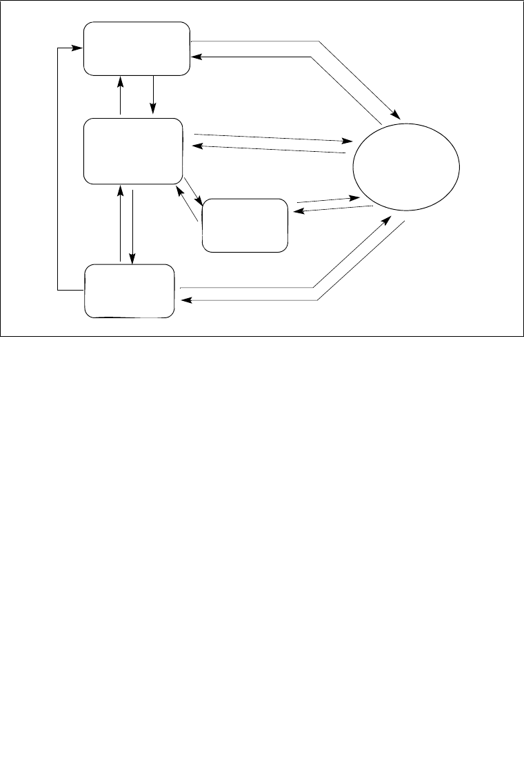
Vol. 3A 2-11
SYSTEM ARCHITECTURE OVERVIEW
The processor is placed in real-address mode following power-up or a reset. The PE flag in
control register CR0 then controls whether the processor is operating in real-address or protected
mode. See also: Section 9.9, “Mode Switching.”
The VM flag in the EFLAGS register determines whether the processor is operating in protected
mode or virtual-8086 mode. Transitions between protected mode and virtual-8086 mode are
generally carried out as part of a task switch or a return from an interrupt or exception handler.
See also: Section 15.2.5, “Entering Virtual-8086 Mode.”
The LMA bit (IA32_EFER.LMA.LMA[bit 10]) determines whether the processor is operating
in IA-32e mode. When running in IA-32e mode, 64-bit or compatibility sub-mode operation is
determined by CS.L bit of the code segment. The processor enters into IA-32e mode from
protected mode by enabling paging and setting the LME bit (IA32_EFER.LME[bit 8]). See also:
Chapter 9, “Processor Management and Initialization.”
The processor switches to SMM whenever it receives an SMI while the processor is in real-
address, protected, virtual-8086, or IA-32e modes. Upon execution of the RSM instruction, the
processor always returns to the mode it was in when the SMI occurred.
Figure 2-3. Transitions Among the Processor’s Operating Modes
Real-Address
Protected Mode
Virtual-8086
Mode
System
Management
Mode
PE=1
Reset or
VM=1VM=0
PE=0
Reset
or
RSM
SMI#
RSM
SMI#
RSM
SMI#
Reset
Mode
IA-32e
Mode
RSM
SMI#
LME=1, CR0.PG=1*
See**
* See Section 9.8.5
** See Section 9.8.5.4
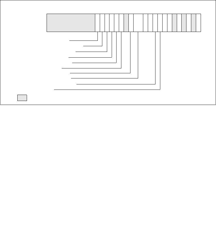
2-12 Vol. 3A
SYSTEM ARCHITECTURE OVERVIEW
2.3 SYSTEM FLAGS AND FIELDS IN THE EFLAGS REGISTER
The system flags and IOPL field of the EFLAGS register control I/O, maskable hardware inter-
rupts, debugging, task switching, and the virtual-8086 mode (see Figure 2-4). Only privileged
code (typically operating system or executive code) should be allowed to modify these bits.
The system flags and IOPL are:
TF Trap (bit 8) — Set to enable single-step mode for debugging; clear to disable single-
step mode. In single-step mode, the processor generates a debug exception after each
instruction. This allows the execution state of a program to be inspected after each
instruction. If an application program sets the TF flag using a POPF, POPFD, or IRET
instruction, a debug exception is generated after the instruction that follows the POPF,
POPFD, or IRET.
IF Interrupt enable (bit 9) — Controls the response of the processor to maskable hard-
ware interrupt requests (see also: Section 5.3.2, “Maskable Hardware Interrupts”). The
flag is set to respond to maskable hardware interrupts; cleared to inhibit maskable hard-
ware interrupts. The IF flag does not affect the generation of exceptions or
nonmaskable interrupts (NMI interrupts). The CPL, IOPL, and the state of the VME
flag in control register CR4 determine whether the IF flag can be modified by the CLI,
STI, POPF, POPFD, and IRET.
IOPL I/O privilege level field (bits 12 and 13) — Indicates the I/O privilege level (IOPL)
of the currently running program or task. The CPL of the currently running program
or task must be less than or equal to the IOPL to access the I/O address space. This
field can only be modified by the POPF and IRET instructions when operating at a
CPL of 0.
Figure 2-4. System Flags in the EFLAGS Register
31 22 21 20 19 18 17 16
R
F
I
DA
CV
M
VM — Virtual-8086 Mode
RF — Resume Flag
NT — Nested Task Flag
IOPL— I/O Privilege Level
IF — Interrupt Enable Flag
AC — Alignment Check
ID — Identification Flag
VIP — Virtual Interrupt Pending
15 13
14 12 11 10 9 876543210
0C
F
A
FP
F1
D
FI
FT
FS
FZ
F
N
T00
V
I
P
V
I
F
O
F
I
O
P
L
VIF — Virtual Interrupt Flag
TF — Trap Flag
Reserved
Reserved (set to 0)

Vol. 3A 2-13
SYSTEM ARCHITECTURE OVERVIEW
The IOPL is also one of the mechanisms that controls the modification of the IF flag
and the handling of interrupts in virtual-8086 mode when virtual mode extensions are
in effect (when CR4.VME = 1). See also: Chapter 13, “Input/Output,” in the IA-32
Intel® Architecture Software Developer’s Manual, Volume 1.
NT Nested task (bit 14) — Controls the chaining of interrupted and called tasks. The
processor sets this flag on calls to a task initiated with a CALL instruction, an interrupt,
or an exception. It examines and modifies this flag on returns from a task initiated with
the IRET instruction. The flag can be explicitly set or cleared with the POPF/POPFD
instructions; however, changing to the state of this flag can generate unexpected excep-
tions in application programs.
See also: Section 6.4, “Task Linking.”
RF Resume (bit 16) — Controls the processor’s response to instruction-breakpoint condi-
tions. When set, this flag temporarily disables debug exceptions (#DB) from being
generated for instruction breakpoints (although other exception conditions can
cause an exception to be generated). When clear, instruction breakpoints will
generate debug exceptions.
The primary function of the RF flag is to allow the restarting of an instruction following
a debug exception that was caused by an instruction breakpoint condition. Here, debug
software must set this flag in the EFLAGS image on the stack just prior to returning to
the interrupted program with IRETD (to prevent the instruction breakpoint from
causing another debug exception). The processor then automatically clears this flag
after the instruction returned to has been successfully executed, enabling instruction
breakpoint faults again.
See also: Section 18.3.1.1, “Instruction-Breakpoint Exception Condition.”
VM Virtual-8086 mode (bit 17) — Set to enable virtual-8086 mode; clear to return to
protected mode.
See also: Section 15.2.1, “Enabling Virtual-8086 Mode.”
AC Alignment check (bit 18) — Set this flag and the AM flag in control register CR0 to
enable alignment checking of memory references; clear the AC flag and/or the AM flag
to disable alignment checking. An alignment-check exception is generated when refer-
ence is made to an unaligned operand, such as a word at an odd byte address or a
doubleword at an address which is not an integral multiple of four. Alignment-check
exceptions are generated only in user mode (privilege level 3). Memory references that
default to privilege level 0, such as segment descriptor loads, do not generate this
exception even when caused by instructions executed in user-mode.
The alignment-check exception can be used to check alignment of data. This is useful
when exchanging data with processors which require all data to be aligned. The align-
ment-check exception can also be used by interpreters to flag some pointers as special
by misaligning the pointer. This eliminates overhead of checking each pointer and only
handles the special pointer when used.

2-14 Vol. 3A
SYSTEM ARCHITECTURE OVERVIEW
VIF Virtual Interrupt (bit 19) — Contains a virtual image of the IF flag. This flag is used
in conjunction with the VIP flag. The processor only recognizes the VIF flag when
either the VME flag or the PVI flag in control register CR4 is set and the IOPL is less
than 3. (The VME flag enables the virtual-8086 mode extensions; the PVI flag enables
the protected-mode virtual interrupts.)
See also: Section 15.3.3.5, “Method 6: Software Interrupt Handling,” and Section 15.4,
“Protected-Mode Virtual Interrupts.”
VIP Virtual interrupt pending (bit 20) — Set by software to indicate that an interrupt is
pending; cleared to indicate that no interrupt is pending. This flag is used in conjunction
with the VIF flag. The processor reads this flag but never modifies it. The processor
only recognizes the VIP flag when either the VME flag or the PVI flag in control
register CR4 is set and the IOPL is less than 3. The VME flag enables the virtual-8086
mode extensions; the PVI flag enables the protected-mode virtual interrupts.
See Section 15.3.3.5, “Method 6: Software Interrupt Handling,” and Section 15.4,
“Protected-Mode Virtual Interrupts.”
ID Identification (bit 21). — The ability of a program or procedure to set or clear this flag
indicates support for the CPUID instruction.
2.3.1 System Flags and Fields in IA-32e Mode
In 64-bit mode, the RFLAGS register expands to 64 bits with the upper 32 bits reserved. System
flags in RFLAGS (64-bit mode) or EFLAGS (compatibility mode) are shown in Figure 2-4.
In IA-32e mode, the processor does not allow the VM bit to be set because virtual-8086 mode
is not supported (attempts to set the bit are ignored). Also, the processor will not set the NT bit.
The processor does, however, allow software to set the NT bit (note that an IRET causes a
general protection fault in IA-32e mode if the NT bit is set).
In IA-32e mode, the SYSCALL/SYSRET instructions have a programmable method of speci-
fying which bits are cleared in RFLAGS/EFLAGS. These instructions save/restore
EFLAGS/RFLAGS.
2.4 MEMORY-MANAGEMENT REGISTERS
The processor provides four memory-management registers (GDTR, LDTR, IDTR, and TR)
that specify the locations of the data structures which control segmented memory management
(see Figure 2-5). Special instructions are provided for loading and storing these registers.

Vol. 3A 2-15
SYSTEM ARCHITECTURE OVERVIEW
2.4.1 Global Descriptor Table Register (GDTR)
The GDTR register holds the base address (32 bits in protected mode; 64 bits in IA-32e mode)
and the 16-bit table limit for the GDT. The base address specifies the linear address of byte 0 of
the GDT; the table limit specifies the number of bytes in the table.
The LGDT and SGDT instructions load and store the GDTR register, respectively. On power up
or reset of the processor, the base address is set to the default value of 0 and the limit is set to
0FFFFH. A new base address must be loaded into the GDTR as part of the processor initializa-
tion process for protected-mode operation.
See also: Section 3.5.1, “Segment Descriptor Tables.”
2.4.2 Local Descriptor Table Register (LDTR)
The LDTR register holds the 16-bit segment selector, base address (32 bits in protected mode;
64 bits in IA-32e mode), segment limit, and descriptor attributes for the LDT. The base address
specifies the linear address of byte 0 of the LDT segment; the segment limit specifies the number
of bytes in the segment. See also: Section 3.5.1, “Segment Descriptor Tables.”
The LLDT and SLDT instructions load and store the segment selector part of the LDTR register,
respectively. The segment that contains the LDT must have a segment descriptor in the GDT.
When the LLDT instruction loads a segment selector in the LDTR: the base address, limit, and
descriptor attributes from the LDT descriptor are automatically loaded in the LDTR.
When a task switch occurs, the LDTR is automatically loaded with the segment selector and
descriptor for the LDT for the new task. The contents of the LDTR are not automatically saved
prior to writing the new LDT information into the register.
On power up or reset of the processor, the segment selector and base address are set to the
default value of 0 and the limit is set to 0FFFFH.
Figure 2-5. Memory Management Registers
0
47(79)
GDTR
IDTR
System Table Registers
32(64)-bit Linear Base Address 16-Bit Table Limit
1516
32(64)-bit Linear Base Address
0
Task
LDTR
System Segment
Seg. Sel.
15
Seg. Sel.
Segment Descriptor Registers (Automatically Loaded)
32(64)-bit Linear Base Address Segment Limit
Attributes
Registers
32(64)-bit Linear Base Address Segment Limit
Register
16-Bit Table Limit

2-16 Vol. 3A
SYSTEM ARCHITECTURE OVERVIEW
2.4.3 IDTR Interrupt Descriptor Table Register
The IDTR register holds the base address (32 bits in protected mode; 64 bits in IA-32e mode)
and 16-bit table limit for the IDT. The base address specifies the linear address of byte 0 of the
IDT; the table limit specifies the number of bytes in the table. The LIDT and SIDT instructions
load and store the IDTR register, respectively. On power up or reset of the processor, the base
address is set to the default value of 0 and the limit is set to 0FFFFH. The base address and limit
in the register can then be changed as part of the processor initialization process.
See also: Section 5.10, “Interrupt Descriptor Table (IDT).”
2.4.4 Task Register (TR)
The task register holds the 16-bit segment selector, base address (32 bits in protected mode; 64
bits in IA-32e mode), segment limit, and descriptor attributes for the TSS of the current task.
The selector references the TSS descriptor in the GDT. The base address specifies the linear
address of byte 0 of the TSS; the segment limit specifies the number of bytes in the TSS. See
also: Section 6.2.4, “Task Register.”
The LTR and STR instructions load and store the segment selector part of the task register,
respectively. When the LTR instruction loads a segment selector in the task register, the base
address, limit, and descriptor attributes from the TSS descriptor are automatically loaded into
the task register. On power up or reset of the processor, the base address is set to the default
value of 0 and the limit is set to 0FFFFH.
When a task switch occurs, the task register is automatically loaded with the segment selector
and descriptor for the TSS for the new task. The contents of the task register are not automati-
cally saved prior to writing the new TSS information into the register.
2.5 CONTROL REGISTERS
Control registers (CR0, CR1, CR2, CR3, and CR4; see Figure 2-6) determine operating mode
of the processor and the characteristics of the currently executing task. These registers are 32
bits in all 32-bit modes and compatibility mode.
In 64-bit mode, control registers are expanded to 64 bits. The MOV CRn instructions are used
to manipulate the register bits. Operand-size prefixes for these instructions are ignored. The
following is also true:
•Bits 63:32 of CR0 and CR4 are reserved and must be written with zeros. Writing a nonzero
value to any of the upper 32 bits results in a general-protection exception, #GP(0).
•All 64 bits of CR2 are writable by software.
•Bits 51:40 of CR3 are reserved and must be 0.
•The MOV CRn instructions do not check that addresses written to CR2 and CR3 are within
the linear-address or physical-address limitations of the implementation.
•Register CR8 is available in 64-bit mode only.

Vol. 3A 2-17
SYSTEM ARCHITECTURE OVERVIEW
The control registers are summarized below, and each architecturally defined control field in
these control registers are described individually. In Figure 2-6, the width of the register in
64-bit mode is indicated in parenthesis (except for CR0).
•CR0 — Contains system control flags that control operating mode and states of the
processor.
•CR1 — Reserved.
•CR2 — Contains the page-fault linear address (the linear address that caused a page fault).
•CR3 — Contains the physical address of the base of the page directory and two flags (PCD
and PWT). This register is also known as the page-directory base register (PDBR). Only
the most-significant bits (less the lower 12 bits) of the base address are specified; the lower
12 bits of the address are assumed to be 0. The page directory must thus be aligned to a
page (4-KByte) boundary. The PCD and PWT flags control caching of the page directory
in the processor’s internal data caches (they do not control TLB caching of page-directory
information).
When using the physical address extension, the CR3 register contains the base address of
the page-directory-pointer table In IA-32e mode, the CR3 register contains the base
address of the PML4 table.
See also: Section 3.8, “36-Bit Physical Addressing Using the PAE Paging Mechanism.”
•CR4 — Contains a group of flags that enable several architectural extensions, and indicate
operating system or executive support for specific processor capabilities. The control
registers can be read and loaded (or modified) using the move-to-or-from-control-registers
forms of the MOV instruction. In protected mode, the MOV instructions allow the control
registers to be read or loaded (at privilege level 0 only). This restriction means that
application programs or operating-system procedures (running at privilege levels 1, 2, or
3) are prevented from reading or loading the control registers.
•CR8 — Provides read and write access to the Task Priority Register (TPR). It specifies the
priority threshold value that operating systems use to control the priority class of external
interrupts allowed to interrupt the processor. This register is available only in 64-bit mode.
However, interrupt filtering continues to apply in compatibility mode.
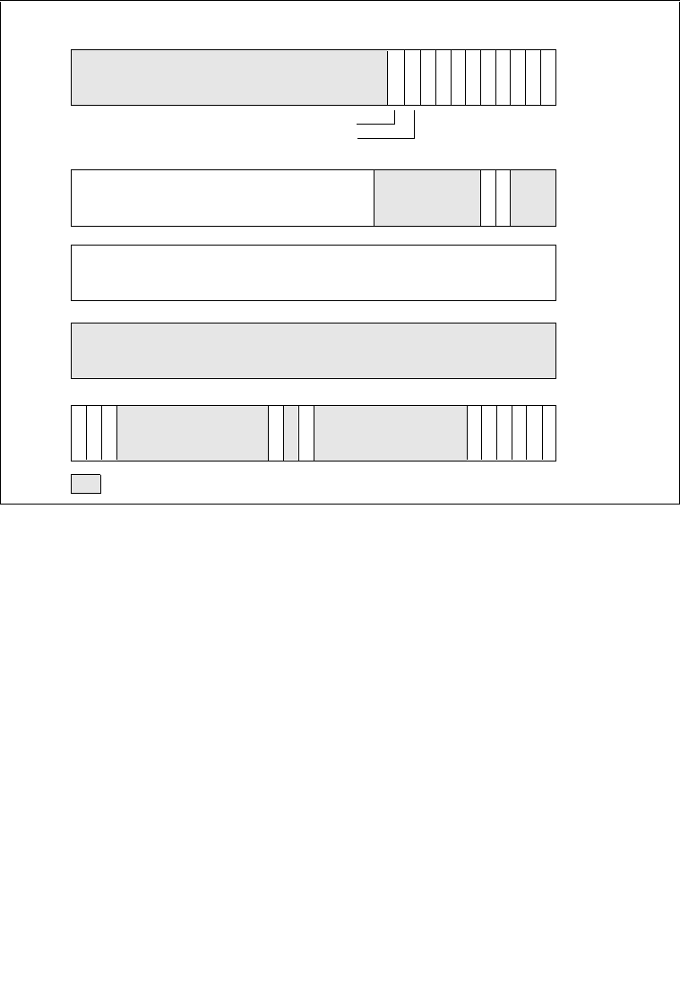
2-18 Vol. 3A
SYSTEM ARCHITECTURE OVERVIEW
When loading a control register, reserved bits should always be set to the values previously read.
The flags in control registers are:
PG Paging (bit 31 of CR0) — Enables paging when set; disables paging when clear.
When paging is disabled, all linear addresses are treated as physical addresses. The PG
flag has no effect if the PE flag (bit 0 of register CR0) is not also set; setting the PG
flag when the PE flag is clear causes a general-protection exception (#GP). See also:
Section 3.6, “Paging (Virtual Memory) Overview.”
On IA-32 processors that support Intel® EM64T, enabling and disabling IA-32e mode
operation also requires modifying CR0.PG.
CD Cache Disable (bit 30 of CR0) — When the CD and NW flags are clear, caching of
memory locations for the whole of physical memory in the processor’s internal (and
external) caches is enabled. When the CD flag is set, caching is restricted as described
in Table 10-5. To prevent the processor from accessing and updating its caches, the CD
flag must be set and the caches must be invalidated so that no cache hits can occur.
See also: Section 10.5.3, “Preventing Caching,” and Section 10.5, “Cache Control.”
Figure 2-6. Control Registers
CR1
W
P
A
M
Page-Directory Base
V
M
E
P
S
E
T
S
D
D
E
P
V
I
P
G
E
M
C
E
P
A
E
P
C
E
N
W
P
GC
D
P
W
T
P
C
D
Page-Fault Linear Address
P
E
E
MM
P
T
S
N
EE
T
CR2
CR0
CR4
Reserved
CR3
Reserved (set to 0)
31 29
30 28 19 18 17 16 15 6543210
31(63) 0
31(63) 0
31(63) 12 11 54320
31(63) 9876543210
(PDBR)
10
OSFXSR
OSXMMEXCPT

Vol. 3A 2-19
SYSTEM ARCHITECTURE OVERVIEW
NW Not Write-through (bit 29 of CR0) — When the NW and CD flags are clear, write-
back (for Pentium 4, Intel Xeon, P6 family, and Pentium processors) or write-through
(for Intel486 processors) is enabled for writes that hit the cache and invalidation cycles
are enabled. See Table 10-5 for detailed information about the affect of the NW flag on
caching for other settings of the CD and NW flags.
AM Alignment Mask (bit 18 of CR0) — Enables automatic alignment checking when set;
disables alignment checking when clear. Alignment checking is performed only when
the AM flag is set, the AC flag in the EFLAGS register is set, CPL is 3, and the
processor is operating in either protected or virtual-8086 mode.
WP Write Protect (bit 16 of CR0) — Inhibits supervisor-level procedures from writing
into user-level read-only pages when set; allows supervisor-level procedures to write
into user-level read-only pages when clear. This flag facilitates implementation of the
copy-on-write method of creating a new process (forking) used by operating systems
such as UNIX*.
NE Numeric Error (bit 5 of CR0) — Enables the native (internal) mechanism for
reporting x87 FPU errors when set; enables the PC-style x87 FPU error reporting
mechanism when clear. When the NE flag is clear and the IGNNE# input is asserted,
x87 FPU errors are ignored. When the NE flag is clear and the IGNNE# input is deas-
serted, an unmasked x87 FPU error causes the processor to assert the FERR# pin to
generate an external interrupt and to stop instruction execution immediately before
executing the next waiting floating-point instruction or WAIT/FWAIT instruction.
The FERR# pin is intended to drive an input to an external interrupt controller (the
FERR# pin emulates the ERROR# pin of the Intel 287 and Intel 387 DX math copro-
cessors). The NE flag, IGNNE# pin, and FERR# pin are used with external logic to
implement PC-style error reporting.
See also: “Software Exception Handling” in Chapter 8, “Programming with the x87
FPU,” and Appendix A, “Eflags Cross-Reference,” in the IA-32 Intel® Architecture
Software Developer’s Manual, Volume 1.
ET Extension Type (bit 4 of CR0) — Reserved in the Pentium 4, Intel Xeon, P6 family,
and Pentium processors. In the Pentium 4, Intel Xeon, and P6 family processors, this
flag is hardcoded to 1. In the Intel386 and Intel486 processors, this flag indicates
support of Intel 387 DX math coprocessor instructions when set.
TS Task Switched (bit 3 of CR0) — Allows the saving of the x87 FPU/MMX/SSE/SSE2/
SSE3 context on a task switch to be delayed until an x87 FPU/MMX/SSE/SSE2/SSE3
instruction is actually executed by the new task. The processor sets this flag on every
task switch and tests it when executing x87 FPU/MMX/SSE/SSE2/SSE3 instructions.
•If the TS flag is set and the EM flag (bit 2 of CR0) is clear, a device-not-available
exception (#NM) is raised prior to the execution of any x87 FPU/MMX/SSE/
SSE2/SSE3 instruction; with the exception of PAUSE, PREFETCHh, SFENCE,
LFENCE, MFENCE, MOVNTI, and CLFLUSH. See the paragraph below for the
special case of the WAIT/FWAIT instructions.
2-20 Vol. 3A
SYSTEM ARCHITECTURE OVERVIEW
•If the TS flag is set and the MP flag (bit 1 of CR0) and EM flag are clear, an #NM
exception is not raised prior to the execution of an x87 FPU WAIT/FWAIT
instruction.
•If the EM flag is set, the setting of the TS flag has no affect on the execution of
x87 FPU/MMX/SSE/SSE2/SSE3 instructions.
Table 2-1 shows the actions taken when the processor encounters an x87 FPU instruc-
tion based on the settings of the TS, EM, and MP flags. Table 11-1 and 12-1 show the
actions taken when the processor encounters an MMX/SSE/SSE2/SSE3 instruction.
The processor does not automatically save the context of the x87 FPU, XMM, and
MXCSR registers on a task switch. Instead, it sets the TS flag, which causes the
processor to raise an #NM exception whenever it encounters an x87 FPU/MMX/SSE
/SSE2/SSE3 instruction in the instruction stream for the new task (with the exception
of the instructions listed above).
The fault handler for the #NM exception can then be used to clear the TS flag (with the CLTS
instruction) and save the context of the x87 FPU, XMM, and MXCSR registers. If the task never
encounters an x87 FPU/MMX/SSE/SSE2/SSE3 instruction; the x87 FPU/MMX/SSE/SSE2/
SSE3 context is never saved.
EM Emulation (bit 2 of CR0) — Indicates that the processor does not have an internal or
external x87 FPU when set; indicates an x87 FPU is present when clear. This flag also
affects the execution of MMX/SSE/SSE2/SSE3 instructions.
When the EM flag is set, execution of an x87 FPU instruction generates a device-not-
available exception (#NM). This flag must be set when the processor does not have an
internal x87 FPU or is not connected to an external math coprocessor. Setting this flag
forces all floating-point instructions to be handled by software emulation. Table 9-2
shows the recommended setting of this flag, depending on the IA-32 processor and x87
Table 2-1. Action Taken By x87 FPU Instructions for Different
Combinations of EM, MP, and TS
CR0 Flags x87 FPU Instruction Type
EM MP TS Floating-Point WAIT/FWAIT
0 0 0 Execute Execute.
0 0 1 #NM Exception Execute.
0 1 0 Execute Execute.
0 1 1 #NM Exception #NM exception.
1 0 0 #NM Exception Execute.
1 0 1 #NM Exception Execute.
1 1 0 #NM Exception Execute.
1 1 1 #NM Exception #NM exception.

Vol. 3A 2-21
SYSTEM ARCHITECTURE OVERVIEW
FPU or math coprocessor present in the system. Table 2-1 shows the interaction of the
EM, MP, and TS flags.
Also, when the EM flag is set, execution of an MMX instruction causes an invalid-
opcode exception (#UD) to be generated (see Table 11-1). Thus, if an IA-32 processor
incorporates MMX technology, the EM flag must be set to 0 to enable execution of
MMX instructions.
Similarly for SSE/SSE2/SSE3 extensions, when the EM flag is set, execution of most
SSE/SSE2/SSE3 instructions causes an invalid opcode exception (#UD) to be gener-
ated (see Table 12-1). If an IA-32 processor incorporates the SSE/SSE2/SSE3 exten-
sions, the EM flag must be set to 0 to enable execution of these extensions.
SSE/SSE2/SSE3 instructions not affected by the EM flag include: PAUSE,
PREFETCHh, SFENCE, LFENCE, MFENCE, MOVNTI, and CLFLUSH.
MP Monitor Coprocessor (bit 1 of CR0). — Controls the interaction of the WAIT (or
FWAIT) instruction with the TS flag (bit 3 of CR0). If the MP flag is set, a WAIT
instruction generates a device-not-available exception (#NM) if the TS flag is also set.
If the MP flag is clear, the WAIT instruction ignores the setting of the TS flag. Table 9-2
shows the recommended setting of this flag, depending on the IA-32 processor and x87
FPU or math coprocessor present in the system. Table 2-1 shows the interaction of the
MP, EM, and TS flags.
PE Protection Enable (bit 0 of CR0) — Enables protected mode when set; enables real-
address mode when clear. This flag does not enable paging directly. It only enables
segment-level protection. To enable paging, both the PE and PG flags must be set.
See also: Section 9.9, “Mode Switching.”
PCD Page-level Cache Disable (bit 4 of CR3) — Controls caching of the current page
directory. When the PCD flag is set, caching of the page-directory is prevented; when
the flag is clear, the page-directory can be cached. This flag affects only the processor’s
internal caches (both L1 and L2, when present). The processor ignores this flag if
paging is not used (the PG flag in register CR0 is clear) or the CD (cache disable) flag
in CR0 is set.
See also: Chapter 10, “Memory Cache Control” (for more about the use of the PCD
flag) and Section 3.7.6, “Page-Directory and Page-Table Entries” (for a description of
a companion PCD flag in page-directory and page-table entries).
PWT Page-level Writes Transparent (bit 3 of CR3) — Controls the write-through or write-
back caching policy of the current page directory. When the PWT flag is set, write-
through caching is enabled; when the flag is clear, write-back caching is enabled. This
flag affects only internal caches (both L1 and L2, when present). The processor ignores
this flag if paging is not used (the PG flag in register CR0 is clear) or the CD (cache
disable) flag in CR0 is set.
See also: Section 10.5, “Cache Control” (for more information about the use of this
flag), and Section 3.7.6, “Page-Directory and Page-Table Entries” (for a description of
a companion PCD flag in the page-directory and page-table entries).

2-22 Vol. 3A
SYSTEM ARCHITECTURE OVERVIEW
VME Virtual-8086 Mode Extensions (bit 0 of CR4) — Enables interrupt- and exception-
handling extensions in virtual-8086 mode when set; disables the extensions when clear.
Use of the virtual mode extensions can improve the performance of virtual-8086 appli-
cations by eliminating the overhead of calling the virtual-8086 monitor to handle inter-
rupts and exceptions that occur while executing an 8086 program and, instead,
redirecting the interrupts and exceptions back to the 8086 program’s handlers. It also
provides hardware support for a virtual interrupt flag (VIF) to improve reliability of
running 8086 programs in multitasking and multiple-processor environments.
See also: Section 15.3, “Interrupt and Exception Handling in Virtual-8086 Mode.”
PVI Protected-Mode Virtual Interrupts (bit 1 of CR4) — Enables hardware support for
a virtual interrupt flag (VIF) in protected mode when set; disables the VIF flag in
protected mode when clear.
See also: Section 15.4, “Protected-Mode Virtual Interrupts.”
TSD Time Stamp Disable (bit 2 of CR4) — Restricts the execution of the RDTSC instruc-
tion to procedures running at privilege level 0 when set; allows RDTSC instruction to
be executed at any privilege level when clear.
DE Debugging Extensions (bit 3 of CR4) — References to debug registers DR4 and DR5
cause an undefined opcode (#UD) exception to be generated when set; when clear,
processor aliases references to registers DR4 and DR5 for compatibility with software
written to run on earlier IA-32 processors.
See also: Section 18.2.2, “Debug Registers DR4 and DR5.”
PSE Page Size Extensions (bit 4 of CR4) — Enables 4-MByte pages when set; restricts
pages to 4 KBytes when clear.
See also: Section 3.6.1, “Paging Options.”
PAE Physical Address Extension (bit 5 of CR4) — When set, enables paging mechanism
to reference greater-or-equal-than-36-bit physical addresses. When clear, restricts
physical addresses to 32 bits. PAE must be enabled to enable IA-32e mode operation.
Enabling and disabling IA-32e mode operation also requires modifying CR4.PAE.
See also: Section 3.8, “36-Bit Physical Addressing Using the PAE Paging
Mechanism.”
MCE Machine-Check Enable (bit 6 of CR4) — Enables the machine-check exception
when set; disables the machine-check exception when clear.
See also: Chapter 14, “Machine-Check Architecture.”
PGE Page Global Enable (bit 7 of CR4) — (Introduced in the P6 family processors.)
Enables the global page feature when set; disables the global page feature when clear.
The global page feature allows frequently used or shared pages to be marked as global
to all users (done with the global flag, bit 8, in a page-directory or page-table entry).
Global pages are not flushed from the translation-lookaside buffer (TLB) on a task
switch or a write to register CR3.

Vol. 3A 2-23
SYSTEM ARCHITECTURE OVERVIEW
When enabling the global page feature, paging must be enabled (by setting the PG flag
in control register CR0) before the PGE flag is set. Reversing this sequence may affect
program correctness, and processor performance will be impacted.
See also: Section 3.12, “Translation Lookaside Buffers (TLBs).”
PCE Performance-Monitoring Counter Enable (bit 8 of CR4) — Enables execution of
the RDPMC instruction for programs or procedures running at any protection level
when set; RDPMC instruction can be executed only at protection level 0 when clear.
OSFXSR
Operating System Support for FXSAVE and FXRSTOR instructions (bit 9 of
CR4) — When set, this flag: (1) indicates to software that the operating system
supports the use of the FXSAVE and FXRSTOR instructions, (2) enables the FXSAVE
and FXRSTOR instructions to save and restore the contents of the XMM and MXCSR
registers along with the contents of the x87 FPU and MMX registers, and (3) enables
the processor to execute SSE/SSE2/SSE3 instructions, with the exception of the
PAUSE, PREFETCHh, SFENCE, LFENCE, MFENCE, MOVNTI, and CLFLUSH.
If this flag is clear, the FXSAVE and FXRSTOR instructions will save and restore the
contents of the x87 FPU and MMX instructions, but they may not save and restore the
contents of the XMM and MXCSR registers. Also, the processor will generate an
invalid opcode exception (#UD) if it attempts to execute any SSE/SSE2/SSE3 instruc-
tion, with the exception of PAUSE, PREFETCHh, SFENCE, LFENCE, MFENCE,
MOVNTI, and CLFLUSH. The operating system or executive must explicitly set this
flag.
NOTE
CPUID feature flags FXSR, SSE, SSE2, and SSE3 indicate availability
of the FXSAVE/FXRESTOR instructions, SSE extensions, SSE2
extensions, and SSE3 extensions respectively. The OSFXSR bit
provides operating system software with a means of enabling these
features and indicating that the operating system supports the features.
OSXMMEXCPT
Operating System Support for Unmasked SIMD Floating-Point Exceptions (bit 10
of CR4) — When set, indicates that the operating system supports the handling of
unmasked SIMD floating-point exceptions through an exception handler that is invoked
when a SIMD floating-point exception (#XF) is generated. SIMD floating-point excep-
tions are only generated by SSE/SSE2/SSE3 SIMD floating-point instructions.
The operating system or executive must explicitly set this flag. If this flag is not set, the
processor will generate an invalid opcode exception (#UD) whenever it detects an
unmasked SIMD floating-point exception.
TPL Task Priority Level (bit 3:0 of CR8) — This sets the threshold value corresponding
to the highest-priority interrupt to be blocked. A value of 0 means all interrupts are
enabled. This field is available in 64-bit mode. A value of 15 means all interrupts will
be disabled.

2-24 Vol. 3A
SYSTEM ARCHITECTURE OVERVIEW
2.5.1 CPUID Qualification of Control Register Flags
The VME, PVI, TSD, DE, PSE, PAE, MCE, PGE, PCE, OSFXSR, and OSXMMEXCPT flags
in control register CR4 are model specific. All of these flags (except the PCE flag) can be qual-
ified with the CPUID instruction to determine if they are implemented on the processor before
they are used.
The CR8 register is available on processors that support Intel EM64T. Support for Intel EM64T
can determined using CPUID.
2.6 SYSTEM INSTRUCTION SUMMARY
System instructions handle system-level functions such as loading system registers, managing
the cache, managing interrupts, or setting up the debug registers. Many of these instructions can
be executed only by operating-system or executive procedures (that is, procedures running at
privilege level 0). Others can be executed at any privilege level and are thus available to appli-
cation programs.
Table 2-2 lists the system instructions and indicates whether they are available and useful for
application programs. These instructions are described in Chapter 3 and Chapter 4 of the IA-32
Intel® Architecture Software Developer’s Manual, Volumes 2A & 2B.
Table 2-2. Summary of System Instructions
Instruction Description Useful to
Application? Protected from
Application?
LLDT Load LDT Register No Yes
SLDT Store LDT Register No No
LGDT Load GDT Register No Yes
SGDT Store GDT Register No No
LTR Load Task Register No Yes
STR Store Task Register No No
LIDT Load IDT Register No Yes
SIDT Store IDT Register No No
MOV CRnLoad and store control registers No Yes
SMSW Store MSW Yes No
LMSW Load MSW No Yes
CLTS Clear TS flag in CR0 No Yes
ARPL Adjust RPL Yes1, 5 No
LAR Load Access Rights Yes No
LSL Load Segment Limit Yes No
VERR Verify for Reading Yes No
VERW Verify for Writing Yes No

Vol. 3A 2-25
SYSTEM ARCHITECTURE OVERVIEW
2.6.1 Loading and Storing System Registers
The GDTR, LDTR, IDTR, and TR registers each have a load and store instruction for loading
data into and storing data from the register:
•LGDT (Load GDTR Register) — Loads the GDT base address and limit from memory
into the GDTR register.
•SGDT (Store GDTR Register) — Stores the GDT base address and limit from the GDTR
register into memory.
•LIDT (Load IDTR Register) — Loads the IDT base address and limit from memory into
the IDTR register.
•SIDT (Load IDTR Register — Stores the IDT base address and limit from the IDTR
register into memory.
•LLDT (Load LDT Register) — Loads the LDT segment selector and segment descriptor
from memory into the LDTR. (The segment selector operand can also be located in a
general-purpose register.)
MOV DRnLoad and store debug registers No Yes
INVD Invalidate cache, no writeback No Yes
WBINVD Invalidate cache, with writeback No Yes
INVLPG Invalidate TLB entry No Yes
HLT Halt Processor No Yes
LOCK (Prefix) Bus Lock Yes No
RSM Return from system management mode No Yes
RDMSR3Read Model-Specific Registers No Yes
WRMSR3Write Model-Specific Registers No Yes
RDPMC4Read Performance-Monitoring Counter Yes Yes2
RDTSC3Read Time-Stamp Counter Yes Yes2
NOTES:
1. Useful to application programs running at a CPL of 1 or 2.
2. The TSD and PCE flags in control register CR4 control access to these instructions by application
programs running at a CPL of 3.
3. These instructions were introduced into the IA-32 Architecture with the Pentium processor.
4. This instruction was introduced into the IA-32 Architecture with the Pentium Pro processor and the
Pentium processor with MMX technology.
5. This instruction is not supported in 64-bit mode.
Table 2-2. Summary of System Instructions (Contd.)
Instruction Description Useful to
Application? Protected from
Application?

2-26 Vol. 3A
SYSTEM ARCHITECTURE OVERVIEW
•SLDT (Store LDT Register) — Stores the LDT segment selector from the LDTR register
into memory or a general-purpose register.
•LTR (Load Task Register) — Loads segment selector and segment descriptor for a TSS
from memory into the task register. (The segment selector operand can also be located in a
general-purpose register.)
•STR (Store Task Register) — Stores the segment selector for the current task TSS from
the task register into memory or a general-purpose register.
The LMSW (load machine status word) and SMSW (store machine status word) instructions
operate on bits 0 through 15 of control register CR0. These instructions are provided for compat-
ibility with the 16-bit Intel 286 processor. Programs written to run on 32-bit IA-32 processors
should not use these instructions. Instead, they should access the control register CR0 using the
MOV instruction.
The CLTS (clear TS flag in CR0) instruction is provided for use in handling a device-not-avail-
able exception (#NM) that occurs when the processor attempts to execute a floating-point
instruction when the TS flag is set. This instruction allows the TS flag to be cleared after the x87
FPU context has been saved, preventing further #NM exceptions. See Section 2.5, “Control
Registers,” for more information on the TS flag.
The control registers (CR0, CR1, CR2, CR3, CR4, and CR8) are loaded using the MOV instruc-
tion. The instruction loads a control register from a general-purpose register or stores the content
of a control register in a general-purpose register.
2.6.2 Verifying of Access Privileges
The processor provides several instructions for examining segment selectors and segment
descriptors to determine if access to their associated segments is allowed. These instructions
duplicate some of the automatic access rights and type checking done by the processor, thus
allowing operating-system or executive software to prevent exceptions from being generated.
The ARPL (adjust RPL) instruction adjusts the RPL (requestor privilege level) of a segment
selector to match that of the program or procedure that supplied the segment selector. See
Section 4.10.4, “Checking Caller Access Privileges (ARPL Instruction),” for a detailed expla-
nation of the function and use of this instruction. Note that ARPL is not supported in 64-bit
mode.
The LAR (load access rights) instruction verifies the accessibility of a specified segment and
loads access rights information from the segment’s segment descriptor into a general-purpose
register. Software can then examine the access rights to determine if the segment type is compat-
ible with its intended use. See Section 4.10.1, “Checking Access Rights (LAR Instruction),” for
a detailed explanation of the function and use of this instruction.
The LSL (load segment limit) instruction verifies the accessibility of a specified segment and
loads the segment limit from the segment’s segment descriptor into a general-purpose register.
Software can then compare the segment limit with an offset into the segment to determine
whether the offset lies within the segment. See Section 4.10.3, “Checking That the Pointer

Vol. 3A 2-27
SYSTEM ARCHITECTURE OVERVIEW
Offset Is Within Limits (LSL Instruction),” for a detailed explanation of the function and use of
this instruction.
The VERR (verify for reading) and VERW (verify for writing) instructions verify if a selected
segment is readable or writable, respectively, at a given CPL. See Section 4.10.2, “Checking
Read/Write Rights (VERR and VERW Instructions),” for a detailed explanation of the function
and use of this instruction.
2.6.3 Loading and Storing Debug Registers
Internal debugging facilities in the processor are controlled by a set of 8 debug registers
(DR0-DR7). The MOV instruction allows setup data to be loaded to and stored from these
registers.
On processors that support Intel EM64T, debug registers DR0-DR7 are 64 bits. In 32-bit modes
and compatibility mode, writes to a debug register fill the upper 32 bits with zeros. Reads return
the lower 32 bits. In 64-bit mode, the upper 32 bits of DR6-DR7 are reserved and must be written
with zeros. Writing one to any of the upper 32 bits causes an exception, #GP(0).
In 64-bit mode, MOV DRn instructions read or write all 64 bits of a debug register (operand-
size prefixes are ignored). All 64 bits of DR0-DR3 are writable by software. However,
MOV DRn instructions do not check that addresses written to DR0-DR3 are in the limits of the
implementation. Address matching is supported only on valid addresses generated by the
processor implementation.
2.6.4 Invalidating Caches and TLBs
The processor provides several instructions for use in explicitly invalidating its caches and TLB
entries. The INVD (invalidate cache with no writeback) instruction invalidates all data and
instruction entries in the internal caches and sends a signal to the external caches indicating that
they should be also be invalidated.
The WBINVD (invalidate cache with writeback) instruction performs the same function as the
INVD instruction, except that it writes back modified lines in its internal caches to memory
before it invalidates the caches. After invalidating the internal caches, WBINVD signals
external caches to write back modified data and invalidate their contents.
The INVLPG (invalidate TLB entry) instruction invalidates (flushes) the TLB entry for a spec-
ified page.
2.6.5 Controlling the Processor
The HLT (halt processor) instruction stops the processor until an enabled interrupt (such as NMI
or SMI, which are normally enabled), a debug exception, the BINIT# signal, the INIT# signal,
or the RESET# signal is received. The processor generates a special bus cycle to indicate that
the halt mode has been entered.

2-28 Vol. 3A
SYSTEM ARCHITECTURE OVERVIEW
Hardware may respond to this signal in a number of ways. An indicator light on the front panel
may be turned on. An NMI interrupt for recording diagnostic information may be generated.
Reset initialization may be invoked (note that the BINIT# pin was introduced with the Pentium
Pro processor). If any non-wake events are pending during shutdown, they will be handled after
the wake event from shutdown is processed (for example, A20M# interrupts).
The LOCK prefix invokes a locked (atomic) read-modify-write operation when modifying a
memory operand. This mechanism is used to allow reliable communications between processors
in multiprocessor systems, as described below:
•In the Pentium processor and earlier IA-32 processors, the LOCK prefix causes the
processor to assert the LOCK# signal during the instruction. This always causes an explicit
bus lock to occur.
•In the Pentium 4, Intel Xeon, and P6 family processors, the locking operation is handled
with either a cache lock or bus lock. If a memory access is cacheable and affects only a
single cache line, a cache lock is invoked and the system bus and the actual memory
location in system memory are not locked during the operation. Here, other Pentium 4,
Intel Xeon, or P6 family processors on the bus write-back any modified data and invalidate
their caches as necessary to maintain system memory coherency. If the memory access is
not cacheable and/or it crosses a cache line boundary, the processor’s LOCK# signal is
asserted and the processor does not respond to requests for bus control during the locked
operation.
The RSM (return from SMM) instruction restores the processor (from a context dump) to the
state it was in prior to an system management mode (SMM) interrupt.
2.6.6 Reading Performance-Monitoring and Time-Stamp
Counters
The RDPMC (read performance-monitoring counter) and RDTSC (read time-stamp counter)
instructions allow application programs to read the processor’s performance-monitoring and
time-stamp counters, respectively. Pentium 4 and Intel Xeon processors have eighteen 40-bit
performance-monitoring counters; P6 family processors have two 40-bit counters.
Use these counters to record either the occurrence or duration of events. Events that can be
monitored are model specific; they may include the number of instructions decoded, interrupts
received, or the number of cache loads. Individual counters can be set up to monitor different
events. Use the system instruction WRMSR to set up values in the one of the 45 ESCRs and one
of the 18 CCCR MSRs (for Pentium 4 and Intel Xeon processors); or in the PerfEvtSel0 or the
PerfEvtSel1 MSR (for the P6 family processors). The RDPMC instruction loads the current
count from the selected counter into the EDX:EAX registers.
The time-stamp counter is a model-specific 64-bit counter that is reset to zero each time the
processor is reset. If not reset, the counter will increment ~9.5 x 10¹⁶ times per year when
the processor is operating at a clock rate of 3GHz. At this clock frequency, it would take
over 190 years for the counter to wrap around. The RDTSC instruction loads the current
count of the time-stamp counter into the EDX:EAX registers.

Vol. 3A 2-29
SYSTEM ARCHITECTURE OVERVIEW
See Section 18.10, “Performance Monitoring Overview,” and Section 18.9, “Time-Stamp
Counter,” for more information about the performance monitoring and time-stamp counters.
The RDTSC instruction was introduced into the IA-32 architecture with the Pentium processor.
The RDPMC instruction was introduced into the IA-32 architecture with the Pentium Pro
processor and the Pentium processor with MMX technology. Earlier Pentium processors have
two performance-monitoring counters, but they can be read only with the RDMSR instruction,
and only at privilege level 0.
2.6.6.1 Reading Counters in 64-Bit Mode
In 64-bit mode, RDTSC operates the same as in protected mode. The count in the time-stamp
counter is stored in EDX:EAX (or RDX[31:0]:RAX[31:0] with RDX[63:32]:RAX[63:32]
cleared).
RDPMC requires an index to specify the offset of the performance-monitoring counter. In 64-bit
mode for Pentium 4 or Intel Xeon processor families, the index is specified in ECX[30:0]. The
current count of the performance-monitoring counter is stored in EDX:EAX (or
RDX[31:0]:RAX[31:0] with RDX[63:32]:RAX[63:32] cleared).
2.6.7 Reading and Writing Model-Specific Registers
The RDMSR (read model-specific register) and WRMSR (write model-specific register)
instructions allow a processor’s 64-bit model-specific registers (MSRs) to be read and written,
respectively. The MSR to be read or written is specified by the value in the ECX register.
RDMSR reads the value from the specified MSR to the EDX:EAX registers; WRMSR writes
the value in the EDX:EAX registers to the specified MSR. RDMSR and WRMSR were intro-
duced into the IA-32 architecture with the Pentium processor.
See Section 9.4, “Model-Specific Registers (MSRs),” for more information.
2.6.7.1 Reading and Writing Model-Specific Registers in 64-Bit Mode
RDMSR and WRMSR require an index to specify the address of an MSR. In 64-bit mode, the
index is 32 bits; it is specified using ECX.

2-30 Vol. 3A
SYSTEM ARCHITECTURE OVERVIEW

3
Protected-Mode
Memory
Management

Vol. 3A 3-1
CHAPTER 3
PROTECTED-MODE MEMORY MANAGEMENT
This chapter describes the IA-32 architecture’s protected-mode memory management facilities,
including the physical memory requirements, segmentation mechanism, and paging mechanism.
See also: Chapter 4, “Protection” (for a description of the processor’s protection mechanism)
and Chapter 15, “8086 Emulation” (for a description of memory addressing protection in real-
address and virtual-8086 modes).
3.1 MEMORY MANAGEMENT OVERVIEW
The memory management facilities of the IA-32 architecture are divided into two parts: segmen-
tation and paging. Segmentation provides a mechanism of isolating individual code, data, and
stack modules so that multiple programs (or tasks) can run on the same processor without inter-
fering with one another. Paging provides a mechanism for implementing a conventional
demand-paged, virtual-memory system where sections of a program’s execution environment
are mapped into physical memory as needed. Paging can also be used to provide isolation
between multiple tasks. When operating in protected mode, some form of segmentation must be
used. There is no mode bit to disable segmentation. The use of paging, however, is optional.
These two mechanisms (segmentation and paging) can be configured to support simple single-
program (or single-task) systems, multitasking systems, or multiple-processor systems that used
shared memory.
As shown in Figure 3-1, segmentation provides a mechanism for dividing the processor’s
addressable memory space (called the linear address space) into smaller protected address
spaces called segments. Segments can be used to hold the code, data, and stack for a program
or to hold system data structures (such as a TSS or LDT). If more than one program (or task) is
running on a processor, each program can be assigned its own set of segments. The processor
then enforces the boundaries between these segments and insures that one program does not
interfere with the execution of another program by writing into the other program’s segments.
The segmentation mechanism also allows typing of segments so that the operations that may be
performed on a particular type of segment can be restricted.
All the segments in a system are contained in the processor’s linear address space. To locate a
byte in a particular segment, a logical address (also called a far pointer) must be provided. A
logical address consists of a segment selector and an offset. The segment selector is a unique
identifier for a segment. Among other things it provides an offset into a descriptor table (such
as the global descriptor table, GDT) to a data structure called a segment descriptor. Each
segment has a segment descriptor, which specifies the size of the segment, the access rights and
privilege level for the segment, the segment type, and the location of the first byte of the segment
in the linear address space (called the base address of the segment). The offset part of the logical
address is added to the base address for the segment to locate a byte within the segment. The
base address plus the offset thus forms a linear address in the processor’s linear address space.
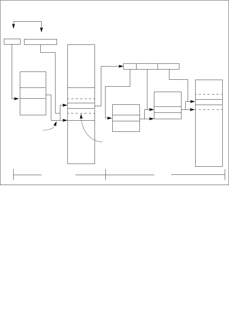
3-2 Vol. 3A
PROTECTED-MODE MEMORY MANAGEMENT
If paging is not used, the linear address space of the processor is mapped directly into the phys-
ical address space of processor. The physical address space is defined as the range of addresses
that the processor can generate on its address bus.
Because multitasking computing systems commonly define a linear address space much larger
than it is economically feasible to contain all at once in physical memory, some method of
“virtualizing” the linear address space is needed. This virtualization of the linear address space
is handled through the processor’s paging mechanism.
Paging supports a “virtual memory” environment where a large linear address space is simulated
with a small amount of physical memory (RAM and ROM) and some disk storage. When using
paging, each segment is divided into pages (typically 4 KBytes each in size), which are stored
either in physical memory or on the disk. The operating system or executive maintains a page
directory and a set of page tables to keep track of the pages. When a program (or task) attempts
to access an address location in the linear address space, the processor uses the page directory
and page tables to translate the linear address into a physical address and then performs the
requested operation (read or write) on the memory location.
Figure 3-1. Segmentation and Paging
Global Descriptor
Table (GDT)
Linear Address
Space
Segment
Segment
Descriptor
Offset
Logical Address
Segment
Base Address
Page
Phy. Addr.
Lin. Addr.
Segment
Selector
Dir Table Offset
Linear Address
Page Table
Page Directory
Entry
Physical
Space
Entry
(or Far Pointer)
Paging
Segmentation
Address
Page

Vol. 3A 3-3
PROTECTED-MODE MEMORY MANAGEMENT
If the page being accessed is not currently in physical memory, the processor interrupts execu-
tion of the program (by generating a page-fault exception). The operating system or executive
then reads the page into physical memory from the disk and continues executing the program.
When paging is implemented properly in the operating-system or executive, the swapping of
pages between physical memory and the disk is transparent to the correct execution of a
program. Even programs written for 16-bit IA-32 processors can be paged (transparently) when
they are run in virtual-8086 mode.
3.2 USING SEGMENTS
The segmentation mechanism supported by the IA-32 architecture can be used to implement a
wide variety of system designs. These designs range from flat models that make only minimal
use of segmentation to protect programs to multi-segmented models that employ segmentation
to create a robust operating environment in which multiple programs and tasks can be executed
reliably.
The following sections give several examples of how segmentation can be employed in a system
to improve memory management performance and reliability.
3.2.1 Basic Flat Model
The simplest memory model for a system is the basic “flat model,” in which the operating
system and application programs have access to a continuous, unsegmented address space. To
the greatest extent possible, this basic flat model hides the segmentation mechanism of the archi-
tecture from both the system designer and the application programmer.
To implement a basic flat memory model with the IA-32 architecture, at least two segment
descriptors must be created, one for referencing a code segment and one for referencing a data
segment (see Figure 3-2). Both of these segments, however, are mapped to the entire linear
address space: that is, both segment descriptors have the same base address value of 0 and the
same segment limit of 4 GBytes. By setting the segment limit to 4 GBytes, the segmentation
mechanism is kept from generating exceptions for out of limit memory references, even if no
physical memory resides at a particular address. ROM (EPROM) is generally located at the top
of the physical address space, because the processor begins execution at FFFF_FFF0H. RAM
(DRAM) is placed at the bottom of the address space because the initial base address for the DS
data segment after reset initialization is 0.
3.2.2 Protected Flat Model
The protected flat model is similar to the basic flat model, except the segment limits are set to
include only the range of addresses for which physical memory actually exists (see Figure 3-3).
A general-protection exception (#GP) is then generated on any attempt to access nonexistent
memory. This model provides a minimum level of hardware protection against some kinds of
program bugs.
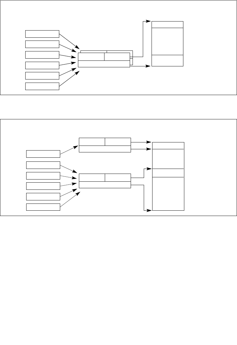
3-4 Vol. 3A
PROTECTED-MODE MEMORY MANAGEMENT
More complexity can be added to this protected flat model to provide more protection. For
example, for the paging mechanism to provide isolation between user and supervisor code and
data, four segments need to be defined: code and data segments at privilege level 3 for the user,
and code and data segments at privilege level 0 for the supervisor. Usually these segments all
overlay each other and start at address 0 in the linear address space. This flat segmentation
model along with a simple paging structure can protect the operating system from applications,
and by adding a separate paging structure for each task or process, it can also protect applica-
tions from each other. Similar designs are used by several popular multitasking operating
systems.
Figure 3-2. Flat Model
Figure 3-3. Protected Flat Model
Linear Address Space
(or Physical Memory)
Data and
FFFFFFFFH
Segment
LimitAccess
Base Address
Registers
CS
SS
DS
ES
FS
GS
Code
0
Code- and Data-Segment
Descriptors
Stack
Not Present
Linear Address Space
(or Physical Memory)
Data and
FFFFFFFFH
Segment
LimitAccess
Base Address
Registers
CS
ES
SS
DS
FS
GS
Code
0
Segment
Descriptors
LimitAccess
Base Address
Memory I/O
Stack
Not Present
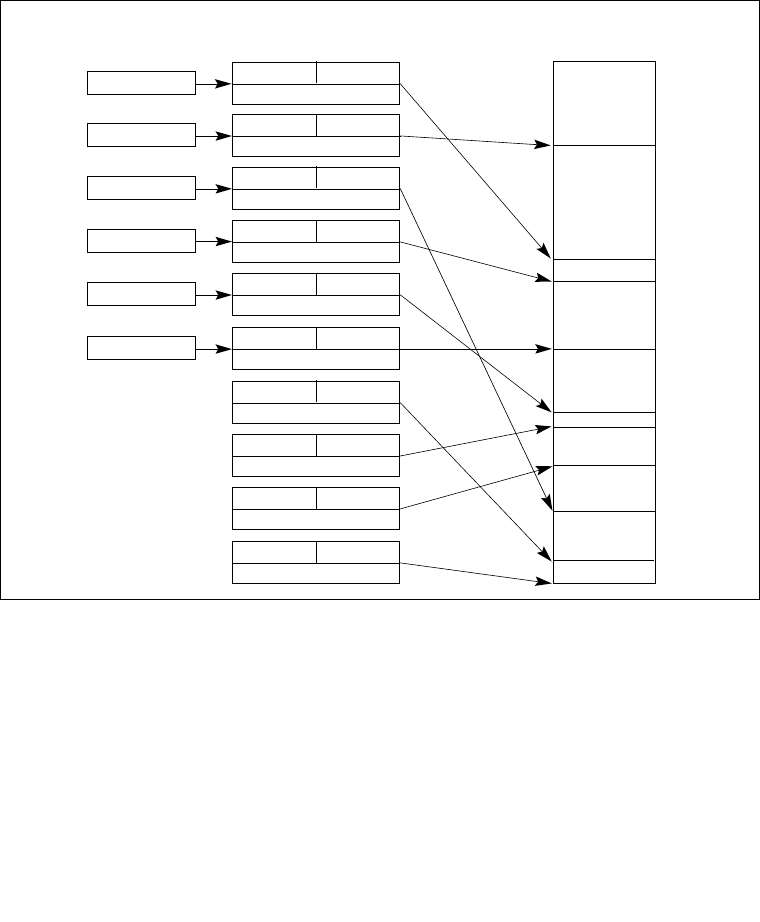
Vol. 3A 3-5
PROTECTED-MODE MEMORY MANAGEMENT
3.2.3 Multi-Segment Model
A multi-segment model (such as the one shown in Figure 3-4) uses the full capabilities of the
segmentation mechanism to provided hardware enforced protection of code, data structures, and
programs and tasks. Here, each program (or task) is given its own table of segment descriptors
and its own segments. The segments can be completely private to their assigned programs or
shared among programs. Access to all segments and to the execution environments of individual
programs running on the system is controlled by hardware.
Access checks can be used to protect not only against referencing an address outside the limit
of a segment, but also against performing disallowed operations in certain segments. For
example, since code segments are designated as read-only segments, hardware can be used to
prevent writes into code segments. The access rights information created for segments can also
be used to set up protection rings or levels. Protection levels can be used to protect operating-
system procedures from unauthorized access by application programs.
Figure 3-4. Multi-Segment Model
Linear Address Space
(or Physical Memory)
Segment
Registers
CS
Segment
Descriptors
LimitAccess
Base Address
SS LimitAccess
Base Address
DS LimitAccess
Base Address
ES LimitAccess
Base Address
FS LimitAccess
Base Address
GS LimitAccess
Base Address
LimitAccess
Base Address
LimitAccess
Base Address
LimitAccess
Base Address
LimitAccess
Base Address
Stack
Code
Data
Data
Data
Data

3-6 Vol. 3A
PROTECTED-MODE MEMORY MANAGEMENT
3.2.4 Segmentation in IA-32e Mode
In IA-32e mode, the effects of segmentation depend on whether the processor is running in
compatibility mode or 64-bit mode. In compatibility mode, segmentation functions just as it
does using legacy 16-bit or 32-bit protected mode semantics.
In 64-bit mode, segmentation is generally (but not completely) disabled, creating a flat 64-bit
linear-address space. The processor treats the segment base of CS, DS, ES, SS as zero, creating
a linear address that is equal to the effective address. The FS and GS segments are exceptions.
These segment registers (which hold the segment base) can be used as an additional base regis-
ters in linear address calculations. They facilitate addressing local data and certain operating
system data structures.
Note that the processor does not perform segment limit checks at runtime in 64-bit mode.
3.2.5 Paging and Segmentation
Paging can be used with any of the segmentation models described in Figures 3-2, 3-3, and 3-4.
The processor’s paging mechanism divides the linear address space (into which segments are
mapped) into pages (as shown in Figure 3-1). These linear-address-space pages are then mapped
to pages in the physical address space. The paging mechanism offers several page-level protec-
tion facilities that can be used with or instead of the segment-protection facilities. For example,
it lets read-write protection be enforced on a page-by-page basis. The paging mechanism also
provides two-level user-supervisor protection that can also be specified on a page-by-page basis.
3.3 PHYSICAL ADDRESS SPACE
In protected mode, the IA-32 architecture provides a normal physical address space of 4 GBytes
(232 bytes). This is the address space that the processor can address on its address bus. This
address space is flat (unsegmented), with addresses ranging continuously from 0 to
FFFFFFFFH. This physical address space can be mapped to read-write memory, read-only
memory, and memory mapped I/O. The memory mapping facilities described in this chapter can
be used to divide this physical memory up into segments and/or pages.
Starting with the Pentium Pro processor, the IA-32 architecture also supports an extension of the
physical address space to 236 bytes (64 GBytes); with a maximum physical address of
FFFFFFFFFH. This extension is invoked in either of two ways:
•Using the physical address extension (PAE) flag, located in bit 5 of control register CR4.
•Using the 36-bit page size extension (PSE-36) feature (introduced in the Pentium III
processors).
See Section 3.8, “36-Bit Physical Addressing Using the PAE Paging Mechanism” and Section 3.9,
“36-Bit Physical Addressing Using the PSE-36 Paging Mechanism” for more information about
36-bit physical addressing.

Vol. 3A 3-7
PROTECTED-MODE MEMORY MANAGEMENT
3.3.1 Physical Address Space for Processors with Intel® EM64T
On processors that support Intel EM64T (CPUID.80000001.EDX[29] = 1), the size of physical
address range is implementation-specific and indicated by CPUID.80000001H. The physical
address size supported by a given implementation is available to IA-32e mode and enhanced
legacy PAE paging.
See also: Section 3.8.1, “Enhanced Legacy PAE Paging”.
3.4 LOGICAL AND LINEAR ADDRESSES
At the system-architecture level in protected mode, the processor uses two stages of address
translation to arrive at a physical address: logical-address translation and linear address space
paging.
Even with the minimum use of segments, every byte in the processor’s address space is accessed
with a logical address. A logical address consists of a 16-bit segment selector and a 32-bit offset
(see Figure 3-5). The segment selector identifies the segment the byte is located in and the offset
specifies the location of the byte in the segment relative to the base address of the segment.
The processor translates every logical address into a linear address. A linear address is a 32-bit
address in the processor’s linear address space. Like the physical address space, the linear
address space is a flat (unsegmented), 232-byte address space, with addresses ranging from 0 to
FFFFFFFFH. The linear address space contains all the segments and system tables defined for
a system.
To translate a logical address into a linear address, the processor does the following:
1. Uses the offset in the segment selector to locate the segment descriptor for the segment in
the GDT or LDT and reads it into the processor. (This step is needed only when a new
segment selector is loaded into a segment register.)
2. Examines the segment descriptor to check the access rights and range of the segment to
insure that the segment is accessible and that the offset is within the limits of the segment.
3. Adds the base address of the segment from the segment descriptor to the offset to form a
linear address.
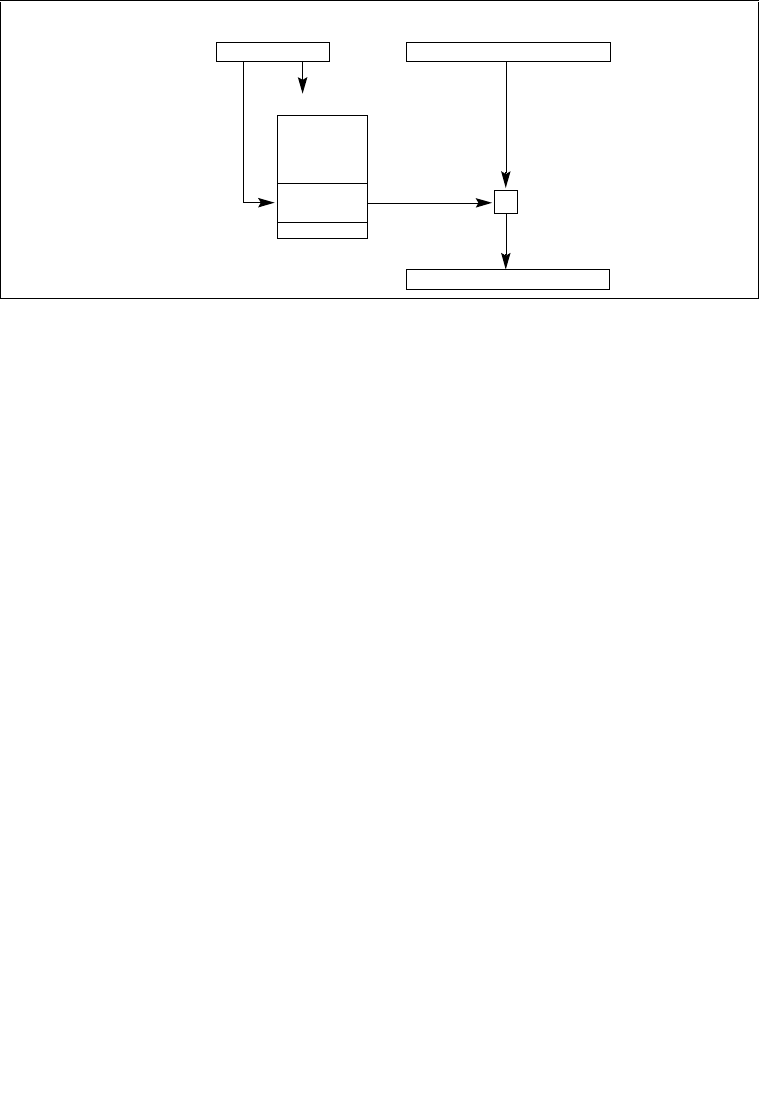
3-8 Vol. 3A
PROTECTED-MODE MEMORY MANAGEMENT
If paging is not used, the processor maps the linear address directly to a physical address (that
is, the linear address goes out on the processor’s address bus). If the linear address space is
paged, a second level of address translation is used to translate the linear address into a physical
address.
See also: Section 3.6, “Paging (Virtual Memory) Overview”.
3.4.1 Logical Address Translation in IA-32e Mode
In IA-32e mode, the processor uses the steps described above to translate a logical address to a
linear address. In 64-bit mode, the offset and base address of the segment are 64-bits instead of
32 bits. The linear address format is also 64 bits wide and is subject to the canonical form
requirement.
Each code segment descriptor provides an L bit. This bit allows a code segment to execute 64-bit
code or legacy 32-bit code by code segment.
3.4.2 Segment Selectors
A segment selector is a 16-bit identifier for a segment (see Figure 3-6). It does not point directly
to the segment, but instead points to the segment descriptor that defines the segment. A segment
selector contains the following items:
Index (Bits 3 through 15) — Selects one of 8192 descriptors in the GDT or LDT. The
processor multiplies the index value by 8 (the number of bytes in a segment
descriptor) and adds the result to the base address of the GDT or LDT (from
the GDTR or LDTR register, respectively).
Figure 3-5. Logical Address to Linear Address Translation
Offset (Effective Address) 0
Base Address
Descriptor Table
Segment
Descriptor
31(63)
Seg. Selector015
Logical
Address
+
Linear Address
031(63)

Vol. 3A 3-9
PROTECTED-MODE MEMORY MANAGEMENT
TI (table indicator) flag
(Bit 2) — Specifies the descriptor table to use: clearing this flag selects the
GDT; setting this flag selects the current LDT.
Requested Privilege Level (RPL)
(Bits 0 and 1) — Specifies the privilege level of the selector. The privilege level
can range from 0 to 3, with 0 being the most privileged level. See Section 4.5,
“Privilege Levels”, for a description of the relationship of the RPL to the CPL
of the executing program (or task) and the descriptor privilege level (DPL) of
the descriptor the segment selector points to.
The first entry of the GDT is not used by the processor. A segment selector that points to this
entry of the GDT (that is, a segment selector with an index of 0 and the TI flag set to 0) is used
as a “null segment selector.” The processor does not generate an exception when a segment
register (other than the CS or SS registers) is loaded with a null selector. It does, however,
generate an exception when a segment register holding a null selector is used to access memory.
A null selector can be used to initialize unused segment registers. Loading the CS or SS register
with a null segment selector causes a general-protection exception (#GP) to be generated.
Segment selectors are visible to application programs as part of a pointer variable, but the values
of selectors are usually assigned or modified by link editors or linking loaders, not application
programs.
3.4.3 Segment Registers
To reduce address translation time and coding complexity, the processor provides registers for
holding up to 6 segment selectors (see Figure 3-7). Each of these segment registers support a
specific kind of memory reference (code, stack, or data). For virtually any kind of program
execution to take place, at least the code-segment (CS), data-segment (DS), and stack-segment
(SS) registers must be loaded with valid segment selectors. The processor also provides three
additional data-segment registers (ES, FS, and GS), which can be used to make additional data
segments available to the currently executing program (or task).
For a program to access a segment, the segment selector for the segment must have been loaded
in one of the segment registers. So, although a system can define thousands of segments, only 6
Figure 3-6. Segment Selector
15 3210
T
I
Index
Table Indicator
0 = GDT
1 = LDT
Requested Privilege Level (RPL)
RPL

3-10 Vol. 3A
PROTECTED-MODE MEMORY MANAGEMENT
can be available for immediate use. Other segments can be made available by loading their
segment selectors into these registers during program execution.
Every segment register has a “visible” part and a “hidden” part. (The hidden part is sometimes
referred to as a “descriptor cache” or a “shadow register.”) When a segment selector is loaded
into the visible part of a segment register, the processor also loads the hidden part of the segment
register with the base address, segment limit, and access control information from the segment
descriptor pointed to by the segment selector. The information cached in the segment register
(visible and hidden) allows the processor to translate addresses without taking extra bus cycles
to read the base address and limit from the segment descriptor. In systems in which multiple
processors have access to the same descriptor tables, it is the responsibility of software to reload
the segment registers when the descriptor tables are modified. If this is not done, an old segment
descriptor cached in a segment register might be used after its memory-resident version has been
modified.
Two kinds of load instructions are provided for loading the segment registers:
1. Direct load instructions such as the MOV, POP, LDS, LES, LSS, LGS, and LFS instruc-
tions. These instructions explicitly reference the segment registers.
2. Implied load instructions such as the far pointer versions of the CALL, JMP, and RET
instructions, the SYSENTER and SYSEXIT instructions, and the IRET, INTn, INTO and
INT3 instructions. These instructions change the contents of the CS register (and
sometimes other segment registers) as an incidental part of their operation.
The MOV instruction can also be used to store visible part of a segment register in a general-
purpose register.
Figure 3-7. Segment Registers
CS
SS
DS
ES
FS
GS
Segment Selector Base Address, Limit, Access Information
Visible Part Hidden Part

Vol. 3A 3-11
PROTECTED-MODE MEMORY MANAGEMENT
3.4.4 Segment Loading Instructions in IA-32e Mode
Because ES, DS, and SS segment registers are not used in 64-bit mode, their fields (base, limit,
and attribute) in segment descriptor registers are ignored. Some forms of segment load instruc-
tions are also invalid (for example, LDS, POP ES). Address calculations that reference the ES,
DS, or SS segments are treated as if the segment base is zero.
The processor checks that all linear-address references are in canonical form instead of
performing limit checks. Mode switching does not change the contents of the segment registers
or the associated descriptor registers. These registers are also not changed during 64-bit mode
execution, unless explicit segment loads are performed.
In order to set up compatibility mode for an application, segment-load instructions (MOV to
Sreg, POP Sreg) work normally in 64-bit mode. An entry is read from the system descriptor
table (GDT or LDT) and is loaded in the hidden portion of the segment descriptor register. The
descriptor-register base, limit, and attribute fields are all loaded. However, the contents of the
data and stack segment selector and the descriptor registers are ignored.
When FS and GS segment overrides are used in 64-bit mode, their respective base addresses are
used in the linear address calculation: (FS or GS).base + index + displacement. FS.base and
GS.base are then expanded to the full linear-address size supported by the implementation. The
resulting effective address calculation can wrap across positive and negative addresses; the
resulting linear address must be canonical.
In 64-bit mode, memory accesses using FS-segment and GS-segment overrides are not checked
for a runtime limit nor subjected to attribute-checking. Normal segment loads (MOV to Sreg and
POP Sreg) into FS and GS load a standard 32-bit base value in the hidden portion of the segment
descriptor register. The base address bits above the standard 32 bits are cleared to 0 to allow
consistency for implementations that use less than 64 bits.
The hidden descriptor register fields for FS.base and GS.base are physically mapped to MSRs
in order to load all address bits supported by a 64-bit implementation. Software with CPL = 0
(privileged software) can load all supported linear-address bits into FS.base or GS.base using
WRMSR. Addresses written into the 64-bit FS.base and GS.base registers must be in canonical
form. A WRMSR instruction that attempts to write a non-canonical address to those registers
causes a #GP fault.
When in compatibility mode, FS and GS overrides operate as defined by 32-bit mode behavior
regardless of the value loaded into the upper 32 linear-address bits of the hidden descriptor
register base field. Compatibility mode ignores the upper 32 bits when calculating an effective
address.
A new 64-bit mode instruction, SWAPGS, can be used to load GS base. SWAPGS exchanges
the kernel data structure pointer from the IA32_KernelGSbase MSR with the GS base register.
The kernel can then use the GS prefix on normal memory references to access the kernel data
structures. An attempt to write a non-canonical value (using WRMSR) to the
IA32_KernelGSBase MSR causes a #GP fault.
3-12 Vol. 3A
PROTECTED-MODE MEMORY MANAGEMENT
3.4.5 Segment Descriptors
A segment descriptor is a data structure in a GDT or LDT that provides the processor with the
size and location of a segment, as well as access control and status information. Segment
descriptors are typically created by compilers, linkers, loaders, or the operating system or exec-
utive, but not application programs. Figure 3-8 illustrates the general descriptor format for all
types of segment descriptors.
The flags and fields in a segment descriptor are as follows:
Segment limit field
Specifies the size of the segment. The processor puts together the two segment
limit fields to form a 20-bit value. The processor interprets the segment limit
in one of two ways, depending on the setting of the G (granularity) flag:
• If the granularity flag is clear, the segment size can range from 1 byte to
1 MByte, in byte increments.
• If the granularity flag is set, the segment size can range from 4 KBytes to
4 GBytes, in 4-KByte increments.
The processor uses the segment limit in two different ways, depending on
whether the segment is an expand-up or an expand-down segment. See Section
3.4.5.1, “Code- and Data-Segment Descriptor Types”, for more information
about segment types. For expand-up segments, the offset in a logical address
can range from 0 to the segment limit. Offsets greater than the segment limit
generate general-protection exceptions (#GP). For expand-down segments, the
Figure 3-8. Segment Descriptor
31 24 23 22 21 20 19 16 15 13
14 12 11 870
P
Base 31:24 GD
P
LTypeS
L4
31 16 15 0
Base Address 15:00 Segment Limit 15:00 0
Base 23:16
D
/
B
A
V
L
Seg.
Limit
19:16
G — Granularity
LIMIT — Segment Limit
P — Segment present
S — Descriptor type (0 = system; 1 = code or data)
TYPE — Segment type
DPL — Descriptor privilege level
AVL — Available for use by system software
BASE — Segment base address
D/B — Default operation size (0 = 16-bit segment; 1 = 32-bit segment)
L — 64-bit code segment (IA-32e mode only)

Vol. 3A 3-13
PROTECTED-MODE MEMORY MANAGEMENT
segment limit has the reverse function; the offset can range from the segment
limit to FFFFFFFFH or FFFFH, depending on the setting of the B flag. Offsets
less than the segment limit generate general-protection exceptions. Decreasing
the value in the segment limit field for an expand-down segment allocates new
memory at the bottom of the segment's address space, rather than at the top.
IA-32 architecture stacks always grow downwards, making this mechanism
convenient for expandable stacks.
Base address fields
Defines the location of byte 0 of the segment within the 4-GByte linear address
space. The processor puts together the three base address fields to form a single
32-bit value. Segment base addresses should be aligned to 16-byte boundaries.
Although 16-byte alignment is not required, this alignment allows programs to
maximize performance by aligning code and data on 16-byte boundaries.
Type field Indicates the segment or gate type and specifies the kinds of access that can be
made to the segment and the direction of growth. The interpretation of this field
depends on whether the descriptor type flag specifies an application (code or
data) descriptor or a system descriptor. The encoding of the type field is
different for code, data, and system descriptors (see Figure 4-1). See Section
3.4.5.1, “Code- and Data-Segment Descriptor Types”, for a description of how
this field is used to specify code and data-segment types.
S (descriptor type) flag
Specifies whether the segment descriptor is for a system segment (S flag is
clear) or a code or data segment (S flag is set).
DPL (descriptor privilege level) field
Specifies the privilege level of the segment. The privilege level can range from
0 to 3, with 0 being the most privileged level. The DPL is used to control access
to the segment. See Section 4.5, “Privilege Levels”, for a description of the
relationship of the DPL to the CPL of the executing code segment and the RPL
of a segment selector.
P (segment-present) flag
Indicates whether the segment is present in memory (set) or not present (clear).
If this flag is clear, the processor generates a segment-not-present exception
(#NP) when a segment selector that points to the segment descriptor is loaded
into a segment register. Memory management software can use this flag to
control which segments are actually loaded into physical memory at a given
time. It offers a control in addition to paging for managing virtual memory.
Figure 3-9 shows the format of a segment descriptor when the segment-present
flag is clear. When this flag is clear, the operating system or executive is free
to use the locations marked “Available” to store its own data, such as informa-
tion regarding the whereabouts of the missing segment.
D/B (default operation size/default stack pointer size and/or upper bound) flag
Performs different functions depending on whether the segment descriptor is
an executable code segment, an expand-down data segment, or a stack
3-14 Vol. 3A
PROTECTED-MODE MEMORY MANAGEMENT
segment. (This flag should always be set to 1 for 32-bit code and data segments
and to 0 for 16-bit code and data segments.)
•Executable code segment. The flag is called the D flag and it indicates the
default length for effective addresses and operands referenced by instruc-
tions in the segment. If the flag is set, 32-bit addresses and 32-bit or 8-bit
operands are assumed; if it is clear, 16-bit addresses and 16-bit or 8-bit
operands are assumed.
The instruction prefix 66H can be used to select an operand size other than
the default, and the prefix 67H can be used select an address size other than
the default.
•Stack segment (data segment pointed to by the SS register). The flag is
called the B (big) flag and it specifies the size of the stack pointer used for
implicit stack operations (such as pushes, pops, and calls). If the flag is set,
a 32-bit stack pointer is used, which is stored in the 32-bit ESP register; if
the flag is clear, a 16-bit stack pointer is used, which is stored in the 16-bit
SP register. If the stack segment is set up to be an expand-down data
segment (described in the next paragraph), the B flag also specifies the
upper bound of the stack segment.
•Expand-down data segment. The flag is called the B flag and it specifies
the upper bound of the segment. If the flag is set, the upper bound is
FFFFFFFFH (4 GBytes); if the flag is clear, the upper bound is FFFFH
(64 KBytes).
G (granularity) flag
Determines the scaling of the segment limit field. When the granularity flag is
clear, the segment limit is interpreted in byte units; when flag is set, the
segment limit is interpreted in 4-KByte units. (This flag does not affect the
granularity of the base address; it is always byte granular.) When the granu-
larity flag is set, the twelve least significant bits of an offset are not tested when
checking the offset against the segment limit. For example, when the granu-
larity flag is set, a limit of 0 results in valid offsets from 0 to 4095.
Figure 3-9. Segment Descriptor When Segment-Present Flag Is Clear
31 16 15 13
14 12 11 870
0
Available D
P
LTypeS4
31 0
Available 0
Available

Vol. 3A 3-15
PROTECTED-MODE MEMORY MANAGEMENT
L (64-bit code segment) flag
In IA-32e mode, bit 21 of the second doubleword of the segment descriptor
indicates whether a code segment contains native 64-bit code. A value of 1
indicates instructions in this code segment are executed in 64-bit mode. A
value of 0 indicates the instructions in this code segment are executed in
compatibility mode. If L-bit is set, then D-bit must be cleared. When not in
IA-32e mode or for non-code segments, bit 21 is reserved and should always
be set to 0.
Available and reserved bits
Bit 20 of the second doubleword of the segment descriptor is available for use
by system software.
3.4.5.1 Code- and Data-Segment Descriptor Types
When the S (descriptor type) flag in a segment descriptor is set, the descriptor is for either a code
or a data segment. The highest order bit of the type field (bit 11 of the second double word of
the segment descriptor) then determines whether the descriptor is for a data segment (clear) or
a code segment (set).
For data segments, the three low-order bits of the type field (bits 8, 9, and 10) are interpreted as
accessed (A), write-enable (W), and expansion-direction (E). See Table 3-1 for a description of
the encoding of the bits in the type field for code and data segments. Data segments can be read-
only or read/write segments, depending on the setting of the write-enable bit.
Table 3-1. Code- and Data-Segment Types
Type Field Descriptor
Type Description
Decimal 11 10
E9
W8
A
0
1
2
3
4
5
6
7
0
0
0
0
0
0
0
0
0
0
0
0
1
1
1
1
0
0
1
1
0
0
1
1
0
1
0
1
0
1
0
1
Data
Data
Data
Data
Data
Data
Data
Data
Read-Only
Read-Only, accessed
Read/Write
Read/Write, accessed
Read-Only, expand-down
Read-Only, expand-down, accessed
Read/Write, expand-down
Read/Write, expand-down, accessed
CRA
8
9
10
11
12
13
14
15
1
1
1
1
1
1
1
1
0
0
0
0
1
1
1
1
0
0
1
1
0
0
1
1
0
1
0
1
0
1
0
1
Code
Code
Code
Code
Code
Code
Code
Code
Execute-Only
Execute-Only, accessed
Execute/Read
Execute/Read, accessed
Execute-Only, conforming
Execute-Only, conforming, accessed
Execute/Read-Only, conforming
Execute/Read-Only, conforming, accessed

3-16 Vol. 3A
PROTECTED-MODE MEMORY MANAGEMENT
Stack segments are data segments which must be read/write segments. Loading the SS register
with a segment selector for a nonwritable data segment generates a general-protection exception
(#GP). If the size of a stack segment needs to be changed dynamically, the stack segment can be
an expand-down data segment (expansion-direction flag set). Here, dynamically changing the
segment limit causes stack space to be added to the bottom of the stack. If the size of a stack
segment is intended to remain static, the stack segment may be either an expand-up or expand-
down type.
The accessed bit indicates whether the segment has been accessed since the last time the oper-
ating-system or executive cleared the bit. The processor sets this bit whenever it loads a segment
selector for the segment into a segment register, assuming that the type of memory that contains
the segment descriptor supports processor writes. The bit remains set until explicitly cleared.
This bit can be used both for virtual memory management and for debugging.
For code segments, the three low-order bits of the type field are interpreted as accessed (A), read
enable (R), and conforming (C). Code segments can be execute-only or execute/read, depending
on the setting of the read-enable bit. An execute/read segment might be used when constants or
other static data have been placed with instruction code in a ROM. Here, data can be read from
the code segment either by using an instruction with a CS override prefix or by loading a
segment selector for the code segment in a data-segment register (the DS, ES, FS, or GS regis-
ters). In protected mode, code segments are not writable.
Code segments can be either conforming or nonconforming. A transfer of execution into a more-
privileged conforming segment allows execution to continue at the current privilege level. A
transfer into a nonconforming segment at a different privilege level results in a general-protec-
tion exception (#GP), unless a call gate or task gate is used (see Section 4.8.1, “Direct Calls or
Jumps to Code Segments”, for more information on conforming and nonconforming code
segments). System utilities that do not access protected facilities and handlers for some types of
exceptions (such as, divide error or overflow) may be loaded in conforming code segments. Util-
ities that need to be protected from less privileged programs and procedures should be placed in
nonconforming code segments.
NOTE
Execution cannot be transferred by a call or a jump to a less-privileged
(numerically higher privilege level) code segment, regardless of whether the
target segment is a conforming or nonconforming code segment. Attempting
such an execution transfer will result in a general-protection exception.
All data segments are nonconforming, meaning that they cannot be accessed by less privileged
programs or procedures (code executing at numerically high privilege levels). Unlike code
segments, however, data segments can be accessed by more privileged programs or procedures
(code executing at numerically lower privilege levels) without using a special access gate.
If the segment descriptors in the GDT or an LDT are placed in ROM, the processor can enter an
indefinite loop if software or the processor attempts to update (write to) the ROM-based
segment descriptors. To prevent this problem, set the accessed bits for all segment descriptors
placed in a ROM. Also, remove operating-system or executive code that attempts to modify
segment descriptors located in ROM.

Vol. 3A 3-17
PROTECTED-MODE MEMORY MANAGEMENT
3.5 SYSTEM DESCRIPTOR TYPES
When the S (descriptor type) flag in a segment descriptor is clear, the descriptor type is a system
descriptor. The processor recognizes the following types of system descriptors:
•Local descriptor-table (LDT) segment descriptor.
•Task-state segment (TSS) descriptor.
•Call-gate descriptor.
•Interrupt-gate descriptor.
•Trap-gate descriptor.
•Task-gate descriptor.
These descriptor types fall into two categories: system-segment descriptors and gate descriptors.
System-segment descriptors point to system segments (LDT and TSS segments). Gate descrip-
tors are in themselves “gates,” which hold pointers to procedure entry points in code segments
(call, interrupt, and trap gates) or which hold segment selectors for TSS’s (task gates).
Table 3-2 shows the encoding of the type field for system-segment descriptors and gate descrip-
tors. Note that system descriptors in IA-32e mode are 16 bytes instead of 8 bytes.
Table 3-2. System-Segment and Gate-Descriptor Types
Type Field Description
Decimal 11 10 9 8 32-Bit Mode IA-32e Mode
0 0000Reserved Upper 8 byte of an 16-byte
descriptor
1 000116-bit TSS (Available) Reserved
2 0010LDT LDT
3 001116-bit TSS (Busy) Reserved
4 010016-bit Call Gate Reserved
5 0101Task Gate Reserved
6 011016-bit Interrupt Gate Reserved
7 011116-bit Trap Gate Reserved
8 1000Reserved Reserved
9 100132-bit TSS (Available) 64-bit TSS (Available)
10 1010Reserved Reserved
11 101132-bit TSS (Busy) 64-bit TSS (Busy)
12 110032-bit Call Gate 64-bit Call Gate
13 1101Reserved Reserved
14 111032-bit Interrupt Gate 64-bit Interrupt Gate
15 111132-bit Trap Gate 64-bit Trap Gate
3-18 Vol. 3A
PROTECTED-MODE MEMORY MANAGEMENT
See also: Section 3.5.1, “Segment Descriptor Tables”, and Section 6.2.2, “TSS Descriptor”
(for more information on the system-segment descriptors); see Section 4.8.3, “Call Gates”,
Section 5.11, “IDT Descriptors”, and Section 6.2.5, “Task-Gate Descriptor” (for more infor-
mation on the gate descriptors).
3.5.1 Segment Descriptor Tables
A segment descriptor table is an array of segment descriptors (see Figure 3-10). A descriptor
table is variable in length and can contain up to 8192 (213) 8-byte descriptors. There are two
kinds of descriptor tables:
•The global descriptor table (GDT)
•The local descriptor tables (LDT)
Figure 3-10. Global and Local Descriptor Tables
Segment
Selector
Global
Descriptor
T
First Descriptor in
GDT is Not Used
TI = 0
I
56
40
48
32
24
16
8
0
TI = 1
56
40
48
32
24
16
8
0
Table (GDT)
Local
Descriptor
Table (LDT)
Base Address
Limit
GDTR Register LDTR Register
Base Address
Seg. Sel.
Limit
Vol. 3A 3-19
PROTECTED-MODE MEMORY MANAGEMENT
Each system must have one GDT defined, which may be used for all programs and tasks in the
system. Optionally, one or more LDTs can be defined. For example, an LDT can be defined for
each separate task being run, or some or all tasks can share the same LDT.
The GDT is not a segment itself; instead, it is a data structure in linear address space. The base
linear address and limit of the GDT must be loaded into the GDTR register (see Section 2.4,
“Memory-Management Registers”). The base addresses of the GDT should be aligned on an
eight-byte boundary to yield the best processor performance. The limit value for the GDT is
expressed in bytes. As with segments, the limit value is added to the base address to get the
address of the last valid byte. A limit value of 0 results in exactly one valid byte. Because
segment descriptors are always 8 bytes long, the GDT limit should always be one less than an
integral multiple of eight (that is, 8N – 1).
The first descriptor in the GDT is not used by the processor. A segment selector to this “null
descriptor” does not generate an exception when loaded into a data-segment register (DS, ES,
FS, or GS), but it always generates a general-protection exception (#GP) when an attempt is
made to access memory using the descriptor. By initializing the segment registers with this
segment selector, accidental reference to unused segment registers can be guaranteed to generate
an exception.
The LDT is located in a system segment of the LDT type. The GDT must contain a segment
descriptor for the LDT segment. If the system supports multiple LDTs, each must have a sepa-
rate segment selector and segment descriptor in the GDT. The segment descriptor for an LDT
can be located anywhere in the GDT. See Section 3.5, “System Descriptor Types”, information
on the LDT segment-descriptor type.
An LDT is accessed with its segment selector. To eliminate address translations when accessing
the LDT, the segment selector, base linear address, limit, and access rights of the LDT are stored
in the LDTR register (see Section 2.4, “Memory-Management Registers”).
When the GDTR register is stored (using the SGDT instruction), a 48-bit “pseudo-descriptor”
is stored in memory (see top diagram in Figure 3-11). To avoid alignment check faults in user
mode (privilege level 3), the pseudo-descriptor should be located at an odd word address (that
is, address MOD 4 is equal to 2). This causes the processor to store an aligned word, followed
by an aligned doubleword. User-mode programs normally do not store pseudo-descriptors, but
the possibility of generating an alignment check fault can be avoided by aligning pseudo-
descriptors in this way. The same alignment should be used when storing the IDTR register
using the SIDT instruction. When storing the LDTR or task register (using the SLTR or STR
instruction, respectively), the pseudo-descriptor should be located at a doubleword address (that
is, address MOD 4 is equal to 0).
Figure 3-11. Pseudo-Descriptor Formats
0
32-bit Base Address Limit
47 1516
0
64-bit Base Address Limit
79 1516

3-20 Vol. 3A
PROTECTED-MODE MEMORY MANAGEMENT
3.5.2 Segment Descriptor Tables in IA-32e Mode
In IA-32e mode, a segment descriptor table can contain up to 8192 (213) 8-byte descriptors. An
entry in the segment descriptor table can be 8 bytes. System descriptors are expanded to 16 bytes
(occupying the space of two entries).
GDTR and LDTR registers are expanded to hold 64-bit base address. The corresponding
pseudo-descriptor is 80 bits. (see the bottom diagram in Figure 3-11).
The following system descriptors expand to 16 bytes:
— Call gate descriptors (see Section 4.8.3.1, “IA-32e Mode Call Gates”)
— IDT gate descriptors (see Section 5.14.1, “64-Bit Mode IDT”)
— LDT and TSS descriptors (see Section 6.2.3, “TSS Descriptor in 64-bit mode”).
3.6 PAGING (VIRTUAL MEMORY) OVERVIEW
When operating in protected mode, IA-32 architecture permits linear address space to be
mapped directly into a large physical memory (for example, 4 GBytes of RAM) or indirectly
(using paging) into a smaller physical memory and disk storage. This latter method of mapping
the linear address space is referred to as virtual memory or demand-paged virtual memory.
When paging is used, the processor divides the linear address space into fixed-size pages (of
4 KBytes, 2 MBytes, or 4 MBytes in length) that can be mapped into physical memory and/or
disk storage. When a program (or task) references a logical address in memory, the processor
translates the address into a linear address and then uses its paging mechanism to translate the
linear address into a corresponding physical address.
If the page containing the linear address is not currently in physical memory, the processor
generates a page-fault exception (#PF). The exception handler for the page-fault exception typi-
cally directs the operating system or executive to load the page from disk storage into physical
memory (perhaps writing a different page from physical memory out to disk in the process).
When the page has been loaded in physical memory, a return from the exception handler causes
the instruction that generated the exception to be restarted. The information that the processor
uses to map linear addresses into the physical address space and to generate page-fault excep-
tions (when necessary) is contained in page directories and page tables stored in memory.
Paging is different from segmentation through its use of fixed-size pages. Unlike segments,
which usually are the same size as the code or data structures they hold, pages have a fixed size.
If segmentation is the only form of address translation used, a data structure present in physical
memory will have all of its parts in memory. If paging is used, a data structure can be partly in
memory and partly in disk storage.
To minimize the number of bus cycles required for address translation, the most recently
accessed page-directory and page-table entries are cached in the processor in devices called
translation lookaside buffers (TLBs). The TLBs satisfy most requests for reading the current
page directory and page tables without requiring a bus cycle. Extra bus cycles occur only when
the TLBs do not contain a page-table entry, which typically happens when a page has not been

Vol. 3A 3-21
PROTECTED-MODE MEMORY MANAGEMENT
accessed for a long time. See Section 3.12, “Translation Lookaside Buffers (TLBs)”, for more
information on the TLBs.
3.6.1 Paging Options
Paging is controlled by three flags in the processor’s control registers:
•PG (paging) flag. Bit 31 of CR0 (available in all IA-32 processors beginning with the
Intel386 processor).
•PSE (page size extensions) flag. Bit 4 of CR4 (introduced in the Pentium processor).
•PAE (physical address extension) flag. Bit 5 of CR4 (introduced in the Pentium Pro
processors).
The PG flag enables the page-translation mechanism. The operating system or executive usually
sets this flag during processor initialization. The PG flag must be set if the processor’s page-
translation mechanism is to be used to implement a demand-paged virtual memory system or if
the operating system is designed to run more than one program (or task) in virtual-8086 mode.
The PSE flag enables large page sizes: 4-MByte pages or 2-MByte pages (when the PAE flag
is set). When the PSE flag is clear, the more common page length of 4 KBytes is used. See
Section 3.7.2, “Linear Address Translation (4-MByte Pages)”, Section 3.8.3, “Linear Address
Translation With PAE Enabled (2-MByte Pages)”, and Section 3.9, “36-Bit Physical Addressing
Using the PSE-36 Paging Mechanism” for more information about the use of the PSE flag.
The PAE flag provides a method of extending physical addresses to 36 bits. This physical
address extension can only be used when paging is enabled. It relies on an additional page direc-
tory pointer table that is used along with page directories and page tables to reference physical
addresses above FFFFFFFFH. See Section 3.8, “36-Bit Physical Addressing Using the PAE
Paging Mechanism”, for more information about extending physical addresses using the PAE
flag.
When PAE is enabled and for processors that support Intel EM64T, the PAE mechanism is
enhanced to support more than 36 bits of physical addressing (if the processor’s implementation
supports more than 36 bits of physical addressing). This applies to IA-32e mode address trans-
lation (see Section 3.10, “PAE-Enabled Paging in IA-32e Mode”) and enhanced legacy PAE-
enabled address translation (see Section 3.8.1, “Enhanced Legacy PAE Paging”).
The 36-bit page size extension (PSE-36) feature provides an alternate method of extending
physical addressing to 36 bits. This paging mechanism uses the page size extension mode
(enabled with the PSE flag) and modified page directory entries to reference physical addresses
above FFFFFFFFH. The PSE-36 feature flag (bit 17 in the EDX register when the CPUID
instruction is executed with a source operand of 1) indicates the availability of this addressing
mechanism. See Section 3.9, “36-Bit Physical Addressing Using the PSE-36 Paging Mecha-
nism”, for more information about the PSE-36 physical address extension and page size exten-
sion mechanism.

3-22 Vol. 3A
PROTECTED-MODE MEMORY MANAGEMENT
3.6.2 Page Tables and Directories in the Absence of Intel EM64T
The information that the processor uses to translate linear addresses into physical addresses
(when paging is enabled) is contained in four data structures:
•Page directory — An array of 32-bit page-directory entries (PDEs) contained in a
4-KByte page. Up to 1024 page-directory entries can be held in a page directory.
•Page table — An array of 32-bit page-table entries (PTEs) contained in a 4-KByte page.
Up to 1024 page-table entries can be held in a page table. (Page tables are not used for
2-MByte or 4-MByte pages. These page sizes are mapped directly from one or more page-
directory entries.)
•Page — A 4-KByte, 2-MByte, or 4-MByte flat address space.
•Page-Directory-Pointer Table — An array of four 64-bit entries, each of which points to
a page directory. This data structure is only used when the physical address extension is
enabled (see Section 3.8, “36-Bit Physical Addressing Using the PAE Paging
Mechanism”).
These tables provide access to either 4-KByte or 4-MByte pages when normal 32-bit physical
addressing is being used and to either 4-KByte or 2-MByte pages or 4-MByte pages only when
extended (36-bit) physical addressing is being used.
Table 3-3 shows the page size and physical address size obtained from various settings of the
paging control flags and the PSE-36 CPUID feature flag. Each page-directory entry contains a
PS (page size) flag that specifies whether the entry points to a page table whose entries in turn
point to 4-KByte pages (PS set to 0) or whether the page-directory entry points directly to a
4-MByte (PSE and PS set to 1) or 2-MByte page (PAE and PS set to 1).
3.7 PAGE TRANSLATION USING 32-BIT PHYSICAL
ADDRESSING
The following sections describe the IA-32 architecture’s page translation mechanism when using
32-bit physical addresses and a maximum physical address space of 4 GBytes. The 32-bit phys-
ical addressing described applies to IA-32 processors that do not support Intel EM64T or when
the following situations are all true:
•The processor supports Intel EM64T but IA-32e mode is not active.
•PAE or PSE mechanism is not active.
Section 3.8, “36-Bit Physical Addressing Using the PAE Paging Mechanism” and Section 3.9,
“36-Bit Physical Addressing Using the PSE-36 Paging Mechanism” describe extensions to this
page translation mechanism to support 36-bit physical addresses and a maximum physical
address space of 64 GBytes.
Vol. 3A 3-23
PROTECTED-MODE MEMORY MANAGEMENT
3.7.1 Linear Address Translation (4-KByte Pages)
Figure 3-12 shows the page directory and page-table hierarchy when mapping linear addresses
to 4-KByte pages. The entries in the page directory point to page tables, and the entries in a page
table point to pages in physical memory. This paging method can be used to address up to 220
pages, which spans a linear address space of 232 bytes (4 GBytes).
Table 3-3. Page Sizes and Physical Address Sizes
PG Flag,
CR0 PAE Flag,
CR4 PSE Flag,
CR4 PS Flag,
PDE PSE-36 CPUID
Feature Flag Page Size Physical Address
Size
0 X X X X — Paging Disabled
1 0 0 X X 4 KBytes 32 Bits
1 0 1 0 X 4 KBytes 32 Bits
1 0 1 1 0 4 MBytes 32 Bits
1 0 1 1 1 4 MBytes 36 Bits
1 1 X 0 X 4 KBytes 36 Bits
1 1 X 1 X 2 MBytes 36 Bits
Figure 3-12. Linear Address Translation (4-KByte Pages)
0
Directory Table Offset
Page Directory
Directory Entry
CR3 (PDBR)
Page Table
Page-Table Entry
4-KByte Page
Physical Address
31 21 111222
Linear Address
1024 PDE ∗ 1024 PTE = 220 Pages
32*
10
12
10
*32 bits aligned onto a 4-KByte boundary.
20
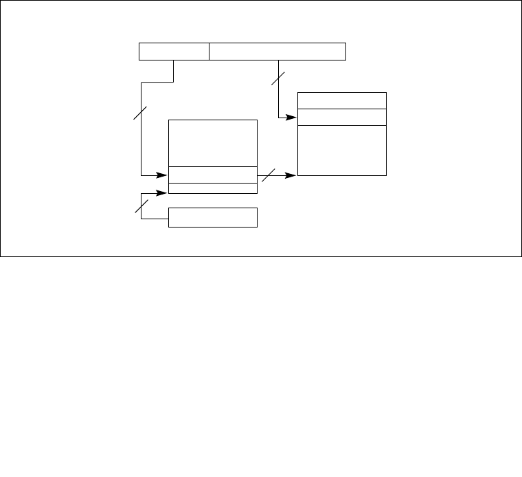
3-24 Vol. 3A
PROTECTED-MODE MEMORY MANAGEMENT
To select the various table entries, the linear address is divided into three sections:
•Page-directory entry — Bits 22 through 31 provide an offset to an entry in the page
directory. The selected entry provides the base physical address of a page table.
•Page-table entry — Bits 12 through 21 of the linear address provide an offset to an entry
in the selected page table. This entry provides the base physical address of a page in
physical memory.
•Page offset — Bits 0 through 11 provides an offset to a physical address in the page.
Memory management software has the option of using one page directory for all programs and
tasks, one page directory for each task, or some combination of the two.
3.7.2 Linear Address Translation (4-MByte Pages)
Figure 3-13 shows how a page directory can be used to map linear addresses to 4-MByte pages.
The entries in the page directory point to 4-MByte pages in physical memory. This paging
method can be used to map up to 1024 pages into a 4-GByte linear address space.
The 4-MByte page size is selected by setting the PSE flag in control register CR4 and setting
the page size (PS) flag in a page-directory entry (see Figure 3-14). With these flags set, the linear
address is divided into two sections:
•Page directory entry—Bits 22 through 31 provide an offset to an entry in the page
directory. The selected entry provides the base physical address of a 4-MByte page.
•Page offset—Bits 0 through 21 provides an offset to a physical address in the page.
Figure 3-13. Linear Address Translation (4-MByte Pages)
0
Directory Offset
Page Directory
Directory Entry
CR3 (PDBR)
4-MByte Page
Physical Address
31 2122
Linear Address
1024 PDE = 1024 Pages
10
22
32*
*32 bits aligned onto a 4-KByte boundary.
10

Vol. 3A 3-25
PROTECTED-MODE MEMORY MANAGEMENT
NOTE
(For the Pentium processor only.) When enabling or disabling large page
sizes, the TLBs must be invalidated (flushed) after the PSE flag in control
register CR4 has been set or cleared. Otherwise, incorrect page translation
might occur due to the processor using outdated page translation information
stored in the TLBs. See Section 10.9, “Invalidating the Translation Lookaside
Buffers (TLBs)”, for information on how to invalidate the TLBs.
3.7.3 Mixing 4-KByte and 4-MByte Pages
When the PSE flag in CR4 is set, both 4-MByte pages and page tables for 4-KByte pages can
be accessed from the same page directory. If the PSE flag is clear, only page tables for 4-KByte
pages can be accessed (regardless of the setting of the PS flag in a page-directory entry).
A typical example of mixing 4-KByte and 4-MByte pages is to place the operating system or
executive’s kernel in a large page to reduce TLB misses and thus improve overall system
performance.
The processor maintains 4-MByte page entries and 4-KByte page entries in separate TLBs. So,
placing often used code such as the kernel in a large page, frees up 4-KByte-page TLB entries
for application programs and tasks.
3.7.4 Memory Aliasing
The IA-32 architecture permits memory aliasing by allowing two page-directory entries to point
to a common page-table entry. Software that needs to implement memory aliasing in this manner
must manage the consistency of the accessed and dirty bits in the page-directory and page-table
entries. Allowing the accessed and dirty bits for the two page-directory entries to become incon-
sistent may lead to a processor deadlock.
3.7.5 Base Address of the Page Directory
The physical address of the current page directory is stored in the CR3 register (also called the
page directory base register or PDBR). (See Figure 2-6 and Section 2.5, “Control Registers”, for
more information on the PDBR.) If paging is to be used, the PDBR must be loaded as part of the
processor initialization process (prior to enabling paging). The PDBR can then be changed
either explicitly by loading a new value in CR3 with a MOV instruction or implicitly as part of
a task switch. (See Section 6.2.1, “Task-State Segment (TSS)”, for a description of how the
contents of the CR3 register is set for a task.)
There is no present flag in the PDBR for the page directory. The page directory may be not-
present (paged out of physical memory) while its associated task is suspended, but the operating
system must ensure that the page directory indicated by the PDBR image in a task's TSS is
present in physical memory before the task is dispatched. The page directory must also remain
in memory as long as the task is active.
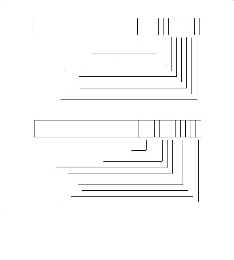
3-26 Vol. 3A
PROTECTED-MODE MEMORY MANAGEMENT
3.7.6 Page-Directory and Page-Table Entries
Figure 3-14 shows the format for the page-directory and page-table entries when 4-KByte
pages and 32-bit physical addresses are being used. Figure 3-15 shows the format for the
page-directory entries when 4-MByte pages and 32-bit physical addresses are being used. The
functions of the flags and fields in the entries in Figures 3-14 and 3-15 are as follows:
Page base address, bits 12 through 32
(Page-table entries for 4-KByte pages) — Specifies the physical address of the
first byte of a 4-KByte page. The bits in this field are interpreted as the 20 most-
significant bits of the physical address, which forces pages to be aligned on
4-KByte boundaries.
Figure 3-14. Format of Page-Directory and Page-Table Entries for 4-KByte Pages
and 32-Bit Physical Addresses
31
Available for system programmer’s use
Global page (Ignored)
Page size (0 indicates 4 KBytes)
Reserved (set to 0)
12 11 9876543210
P
S
P
CA0
Accessed
Cache disabled
Write-through
User/Supervisor
Read/Write
Present
DP
P
W
T
U
/
S
R
/
W
GAvailPage-Table Base Address
31
Available for system programmer’s use
Global Page
Page Table Attribute Index
Dirty
12 11 9 876543210
P
C
AD
Accessed
Cache Disabled
Write-Through
User/Supervisor
Read/Write
Present
DP
P
W
T
U
/
S
R
/
W
AvailPage Base Address
Page-Directory Entry (4-KByte Page Table)
Page-Table Entry (4-KByte Page)
P
A
T
G
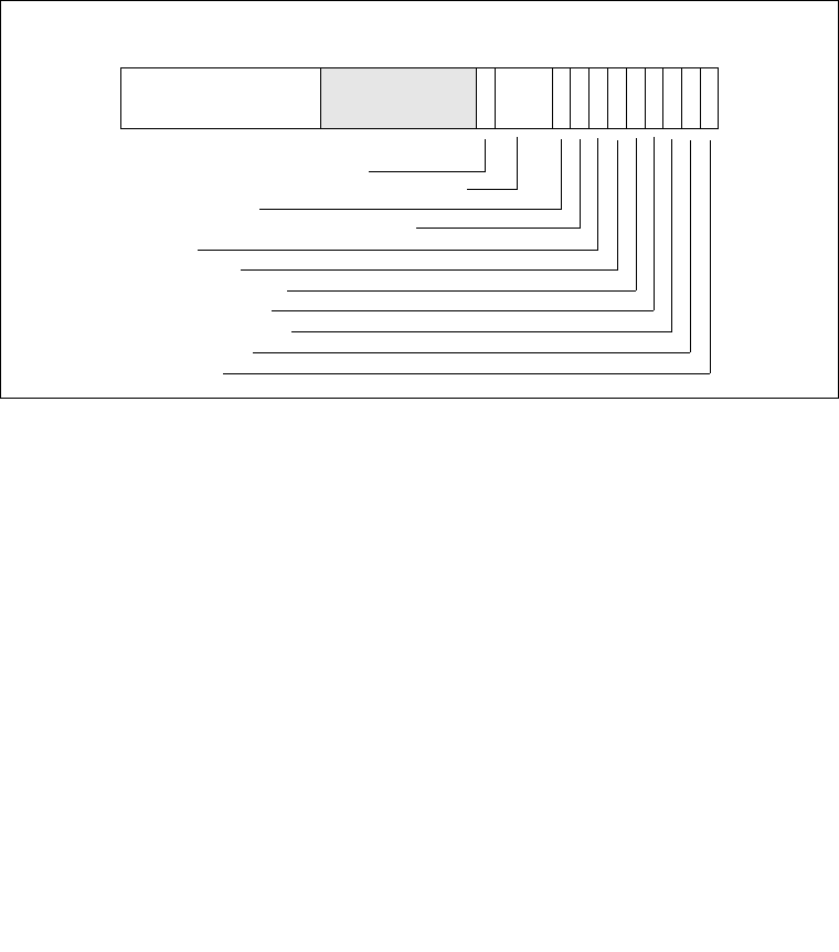
Vol. 3A 3-27
PROTECTED-MODE MEMORY MANAGEMENT
(Page-directory entries for 4-KByte page tables) — Specifies the physical
address of the first byte of a page table. The bits in this field are interpreted as
the 20 most-significant bits of the physical address, which forces page tables to
be aligned on 4-KByte boundaries.
(Page-directory entries for 4-MByte pages) — Specifies the physical address
of the first byte of a 4-MByte page. Only bits 22 through 31 of this field are
used (and bits 12 through 21 are reserved and must be set to 0, for IA-32
processors through the Pentium II processor). The base address bits are inter-
preted as the 10 most-significant bits of the physical address, which forces
4-MByte pages to be aligned on 4-MByte boundaries.
Present (P) flag, bit 0
Indicates whether the page or page table being pointed to by the entry is
currently loaded in physical memory. When the flag is set, the page is in phys-
ical memory and address translation is carried out. When the flag is clear, the
page is not in memory and, if the processor attempts to access the page, it
generates a page-fault exception (#PF).
The processor does not set or clear this flag; it is up to the operating system or
executive to maintain the state of the flag.
If the processor generates a page-fault exception, the operating system gener-
ally needs to carry out the following operations:
1. Copy the page from disk storage into physical memory.
2. Load the page address into the page-table or page-directory entry and set
its present flag. Other flags, such as the dirty and accessed flags, may also
be set at this time.
Figure 3-15. Format of Page-Directory Entries for 4-MByte Pages and 32-Bit Addresses
31
Available for system programmer’s use
Global page
Page size (1 indicates 4 MBytes)
Dirty
12 11 9876543210
P
S
P
CAD
Accessed
Cache disabled
Write-through
User/Supervisor
Read/Write
Present
DP
P
W
T
U
/
S
R
/
W
GAvail.Page Base Address
Page-Directory Entry (4-MByte Page)
22 21
Reserved
Page Table Attribute Index
P
A
T
13

3-28 Vol. 3A
PROTECTED-MODE MEMORY MANAGEMENT
3. Invalidate the current page-table entry in the TLB (see Section 3.12,
“Translation Lookaside Buffers (TLBs)”, for a discussion of TLBs and
how to invalidate them).
4. Return from the page-fault handler to restart the interrupted program (or
task).
Read/write (R/W) flag, bit 1
Specifies the read-write privileges for a page or group of pages (in the case of
a page-directory entry that points to a page table). When this flag is clear, the
page is read only; when the flag is set, the page can be read and written into.
This flag interacts with the U/S flag and the WP flag in register CR0. See
Section 4.11, “Page-Level Protection”, and Table 4-3 for a detailed discussion
of the use of these flags.
User/supervisor (U/S) flag, bit 2
Specifies the user-supervisor privileges for a page or group of pages (in the
case of a page-directory entry that points to a page table). When this flag is
clear, the page is assigned the supervisor privilege level; when the flag is set,
the page is assigned the user privilege level. This flag interacts with the R/W
flag and the WP flag in register CR0. See Section 4.11, “Page-Level Protec-
tion”, and Table 4-3 for a detail discussion of the use of these flags.
Page-level write-through (PWT) flag, bit 3
Controls the write-through or write-back caching policy of individual pages or
page tables. When the PWT flag is set, write-through caching is enabled for the
associated page or page table; when the flag is clear, write-back caching is
enabled for the associated page or page table. The processor ignores this flag if
the CD (cache disable) flag in CR0 is set. See Section 10.5, “Cache Control”,
for more information about the use of this flag. See Section 2.5, “Control
Registers”, for a description of a companion PWT flag in control register CR3.
Page-level cache disable (PCD) flag, bit 4
Controls the caching of individual pages or page tables. When the PCD flag is
set, caching of the associated page or page table is prevented; when the flag is
clear, the page or page table can be cached. This flag permits caching to be
disabled for pages that contain memory-mapped I/O ports or that do not
provide a performance benefit when cached. The processor ignores this flag
(assumes it is set) if the CD (cache disable) flag in CR0 is set. See Chapter 10,
“Memory Cache Control”, for more information about the use of this flag. See
Section 2.5, “Control Registers”, for a description of a companion PCD flag in
control register CR3.
Accessed (A) flag, bit 5
Indicates whether a page or page table has been accessed (read from or written
to) when set. Memory management software typically clears this flag when a
page or page table is initially loaded into physical memory. The processor then
sets this flag the first time a page or page table is accessed.

Vol. 3A 3-29
PROTECTED-MODE MEMORY MANAGEMENT
This flag is a “sticky” flag, meaning that once set, the processor does not
implicitly clear it. Only software can clear this flag. The accessed and dirty
flags are provided for use by memory management software to manage the
transfer of pages and page tables into and out of physical memory.
NOTE: The accesses used by the processor to set this bit may or may not be
exposed to the processor’s Self-Modifying Code detection logic. If the
processor is executing code from the same memory area that is being used for
page table structures, the setting of the bit may or may not result in an imme-
diate change to the executing code stream.
Dirty (D) flag, bit 6
Indicates whether a page has been written to when set. (This flag is not used in
page-directory entries that point to page tables.) Memory management soft-
ware typically clears this flag when a page is initially loaded into physical
memory. The processor then sets this flag the first time a page is accessed for
a write operation.
This flag is “sticky,” meaning that once set, the processor does not implicitly
clear it. Only software can clear this flag. The dirty and accessed flags are
provided for use by memory management software to manage the transfer of
pages and page tables into and out of physical memory.
NOTE: The accesses used by the processor to set this bit may or may not be
exposed to the processor’s Self-Modifying Code detection logic. If the
processor is executing code from the same memory area that is being used for
page table structures, the setting of the bit may or may not result in an imme-
diate change to the executing code stream.
Page size (PS) flag, bit 7 page-directory entries for 4-KByte pages
Determines the page size. When this flag is clear, the page size is 4 KBytes and
the page-directory entry points to a page table. When the flag is set, the page
size is 4 MBytes for normal 32-bit addressing (and 2 MBytes if extended phys-
ical addressing is enabled) and the page-directory entry points to a page. If the
page-directory entry points to a page table, all the pages associated with that
page table will be 4-KByte pages.
Page attribute table index (PAT) flag, bit 7 in page-table entries for 4-KByte pages and
bit 12 in page-directory entries for 4-MByte pages
(Introduced in the Pentium III processor) — Selects PAT entry. For processors
that support the page attribute table (PAT), this flag is used along with the
PCD and PWT flags to select an entry in the PAT, which in turn selects the
memory type for the page (see Section 10.12, “Page Attribute Table (PAT)”).
For processors that do not support the PAT, this bit is reserved and should be
set to 0.
Global (G) flag, bit 8
(Introduced in the Pentium Pro processor) — Indicates a global page when set.
When a page is marked global and the page global enable (PGE) flag in register
CR4 is set, the page-table or page-directory entry for the page is not invalidated
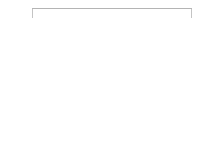
3-30 Vol. 3A
PROTECTED-MODE MEMORY MANAGEMENT
in the TLB when register CR3 is loaded or a task switch occurs. This flag is
provided to prevent frequently used pages (such as pages that contain kernel or
other operating system or executive code) from being flushed from the TLB.
Only software can set or clear this flag. For page-directory entries that point to
page tables, this flag is ignored and the global characteristics of a page are set
in the page-table entries. See Section 3.12, “Translation Lookaside Buffers
(TLBs)”, for more information about the use of this flag. (This bit is reserved
in Pentium and earlier IA-32 processors.)
Reserved and available-to-software bits
For all IA-32 processors. Bits 9, 10, and 11 are available for use by software.
(When the present bit is clear, bits 1 through 31 are available to software, see
Figure 3-16.) In a page-directory entry that points to a page table, bit 6 is
reserved and should be set to 0. When the PSE and PAE flags in control register
CR4 are set, the processor generates a page fault if reserved bits are not set to 0.
For Pentium II and earlier processors. Bit 7 in a page-table entry is reserved and
should be set to 0. For a page-directory entry for a 4-MByte page, bits 12
through 21 are reserved and must be set to 0.
For Pentium III and later processors. For a page-directory entry for a 4-MByte
page, bits 13 through 21 are reserved and must be set to 0.
3.7.7 Not Present Page-Directory and Page-Table Entries
When the present flag is clear for a page-table or page-directory entry, the operating system or
executive may use the rest of the entry for storage of information such as the location of the page
in the disk storage system (see Figure 3-16).
3.8 36-BIT PHYSICAL ADDRESSING USING THE PAE PAGING
MECHANISM
The PAE paging mechanism and support for 36-bit physical addressing were introduced into the
IA-32 architecture in the Pentium Pro processors. Implementation of this feature in an IA-32
processor is indicated with CPUID feature flag PAE (bit 6 in the EDX register when the source
operand for the CPUID instruction is 2). The physical address extension (PAE) flag in register
CR4 enables the PAE mechanism and extends physical addresses from 32 bits to 36 bits. Here,
the processor provides 4 additional address line pins to accommodate the additional address bits.
To use this option, the following flags must be set:
•PG flag (bit 31) in control register CR0—Enables paging
•PAE flag (bit 5) in control register CR4 are set—Enables the PAE paging mechanism.
Figure 3-16. Format of a Page-Table or Page-Directory Entry for a Not-Present Page
31 0
0Available to Operating System or Executive
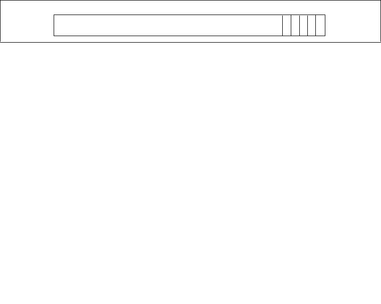
Vol. 3A 3-31
PROTECTED-MODE MEMORY MANAGEMENT
When the PAE paging mechanism is enabled, the processor supports two sizes of pages:
4-KByte and 2-MByte. As with 32-bit addressing, both page sizes can be addressed within the
same set of paging tables (that is, a page-directory entry can point to either a 2-MByte page or
a page table that in turn points to 4-KByte pages). To support the 36-bit physical addresses, the
following changes are made to the paging data structures:
•The paging table entries are increased to 64 bits to accommodate 36-bit base physical
addresses. Each 4-KByte page directory and page table can thus have up to 512 entries.
•A new table, called the page-directory-pointer table, is added to the linear-address
translation hierarchy. This table has 4 entries of 64-bits each, and it lies above the page
directory in the hierarchy. With the physical address extension mechanism enabled, the
processor supports up to 4 page directories.
•The 20-bit page-directory base address field in register CR3 (PDBR) is replaced with a
27-bit page-directory-pointer-table base address field. The updated field provides the 27
most-significant bits of the physical address of the first byte of the page-directory pointer
table (forcing the table to be located on a 32-byte boundary).
Since CR3 now contains the page-directory-pointer-table base address, it can be referred to
as the page-directory-pointer-table register (PDPTR). See Figure 3-17.
•Linear address translation is changed to allow mapping 32-bit linear addresses into the
larger physical address space.
3.8.1 Enhanced Legacy PAE Paging
On processors that support Intel EM64T, the page directory pointer entry supports physical
address size of the underlying implementation (reported by CPUID.80000008H). Legacy PAE
enabled paging (see Section 3.8.2, “Linear Address Translation With PAE Enabled (4-KByte
Pages)” and Section 3.8.3, “Linear Address Translation With PAE Enabled (2-MByte Pages)”
can address physical memory greater than 64-GByte if the implementation’s physical address
size is greater than 36 bits and if the processor supports Intel EM64T.
3.8.2 Linear Address Translation With PAE Enabled (4-KByte
Pages)
Figure 3-18 shows the page-directory-pointer, page-directory, and page-table hierarchy when
mapping linear addresses to 4-KByte pages when the PAE paging mechanism enabled. This
paging method can be used to address up to 220 pages, which spans a linear address space of 232
bytes (4 GBytes).
Figure 3-17. Register CR3 Format When the Physical Address Extension is Enabled
31 0
0
Page-Directory-Pointer-Table Base Address P
C
D
P
W
T00
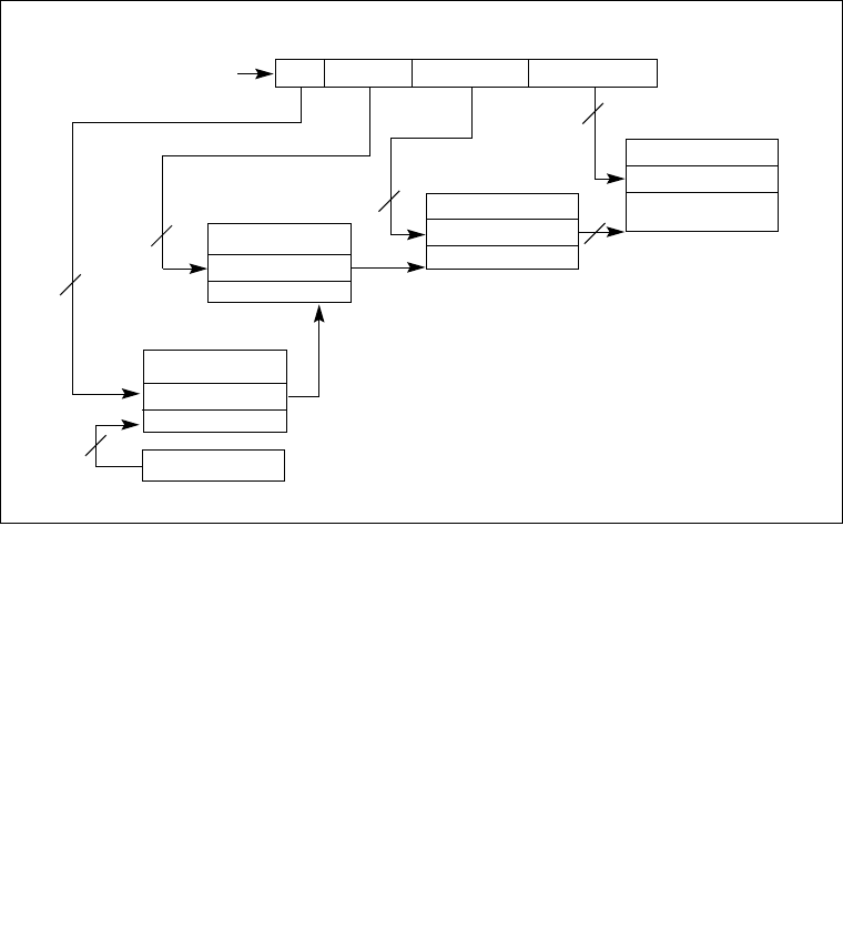
3-32 Vol. 3A
PROTECTED-MODE MEMORY MANAGEMENT
To select the various table entries, the linear address is divided into three sections:
•Page-directory-pointer-table entry—Bits 30 and 31 provide an offset to one of the 4 entries
in the page-directory-pointer table. The selected entry provides the base physical address
of a page directory.
•Page-directory entry—Bits 21 through 29 provide an offset to an entry in the selected page
directory. The selected entry provides the base physical address of a page table.
•Page-table entry—Bits 12 through 20 provide an offset to an entry in the selected page
table. This entry provides the base physical address of a page in physical memory.
•Page offset—Bits 0 through 11 provide an offset to a physical address in the page.
3.8.3 Linear Address Translation With PAE Enabled (2-MByte
Pages)
Figure 3-19 shows how a page-directory-pointer table and page directories can be used to map
linear addresses to 2-MByte pages when the PAE paging mechanism enabled. This paging
method can be used to map up to 2048 pages (4 page-directory-pointer-table entries times 512
page-directory entries) into a 4-GByte linear address space.
When PAE is enabled, the 2-MByte page size is selected by setting the page size (PS) flag in a
page-directory entry (see Figure 3-14). (As shown in Table 3-3, the PSE flag in control register
Figure 3-18. Linear Address Translation With PAE Enabled (4-KByte Pages)
0
Directory Table Offset
Page Directory
Directory Entry
Page Table
Page-Table Entry
4-KByte Page
Physical Address
31 20 111221
Linear Address
Page-Directory-
Dir. Pointer Entry
CR3 (PDPTR)
30 29
Pointer Table
Directory Pointer
4 PDPTE ∗ 512 PDE ∗ 512 PTE = 220 Pages
2
9
32*
12
9
*32 bits aligned onto a 32-byte boundary
24
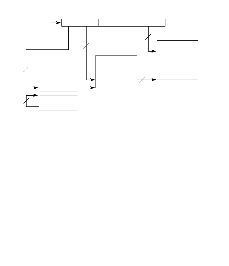
Vol. 3A 3-33
PROTECTED-MODE MEMORY MANAGEMENT
CR4 has no affect on the page size when PAE is enabled.) With the PS flag set, the linear address
is divided into three sections:
•Page-directory-pointer-table entry—Bits 30 and 31 provide an offset to an entry in the
page-directory-pointer table. The selected entry provides the base physical address of a
page directory.
•Page-directory entry—Bits 21 through 29 provide an offset to an entry in the page
directory. The selected entry provides the base physical address of a 2-MByte page.
•Page offset—Bits 0 through 20 provides an offset to a physical address in the page.
3.8.4 Accessing the Full Extended Physical Address Space
With the Extended Page-Table Structure
The page-table structure described in the previous two sections allows up to 4 GBytes of
the 64 GByte extended physical address space to be addressed at one time. Additional 4-GByte
sections of physical memory can be addressed in either of two way:
•Change the pointer in register CR3 to point to another page-directory-pointer table, which
in turn points to another set of page directories and page tables.
•Change entries in the page-directory-pointer table to point to other page directories, which
in turn point to other sets of page tables.
Figure 3-19. Linear Address Translation With PAE Enabled (2-MByte Pages)
0
Directory Offset
Page Directory
Directory Entry
2-MByte Page
Physical Address
31 2021
Linear Address
Page-Directory-
Dir. Pointer Entry
CR3 (PDPTR)
30 29
Pointer Table
Directory
Pointer
4 PDPTE ∗ 512 PDE = 2048 Pages
2
32*
9
21
*32 bits aligned onto a 32-byte boundary
15

3-34 Vol. 3A
PROTECTED-MODE MEMORY MANAGEMENT
3.8.5 Page-Directory and Page-Table Entries With Extended
Addressing Enabled
Figure 3-20 shows the format for the page-directory-pointer-table, page-directory, and
page-table entries when 4-KByte pages and 36-bit extended physical addresses are being
used. Figure 3-21 shows the format for the page-directory-pointer-table and page-directory
entries when 2-MByte pages and 36-bit extended physical addresses are being used. The func-
tions of the flags in these entries are the same as described in Section 3.7.6, “Page-Directory and
Page-Table Entries”. The major differences in these entries are as follows:
•A page-directory-pointer-table entry is added.
•The size of the entries are increased from 32 bits to 64 bits.
•The maximum number of entries in a page directory or page table is 512.
•The base physical address field in each entry is extended to 24 bits.
NOTE
Older IA-32 processors that implement the PAE mechanism use uncached
accesses when loading page-directory-pointer table entries. This behavior is
model specific and not architectural. More recent IA-32 processors may
cache page-directory-pointer table entries.
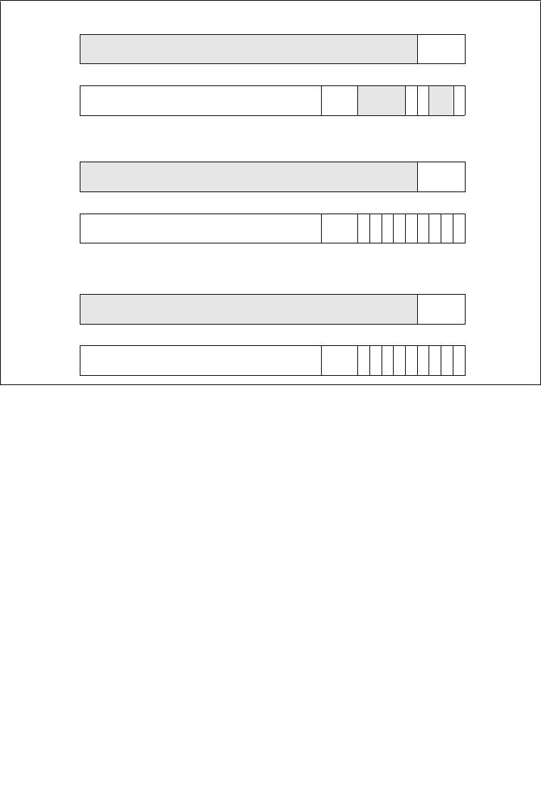
Vol. 3A 3-35
PROTECTED-MODE MEMORY MANAGEMENT
Figure 3-20. Format of Page-Directory-Pointer-Table, Page-Directory, and Page-Table
Entries for 4-KByte Pages with PAE Enabled
63 36 35 32
Base
Reserved (set to 0)
Page-Directory-Pointer-Table Entry
31 12 11 9854320
P
C
D
P
W
T
Avail
Page-Directory Base Address
Addr.
Res.Reserved
63 36 35 32
Base
Reserved (set to 0)
Page-Directory Entry (4-KByte Page Table)
31 12 11 9876543210
P
C
0DP
P
W
T
Page-Table Base Address
Addr.
00 A R
/
W
U
/
S
63 36 35 32
Base
Reserved (set to 0)
Page-Table Entry (4-KByte Page)
31 12 11 9876543210
P
C
DDP
P
W
T
Page Base Address
Addr.
GA R
/
W
U
/
S
Avail
Avail
P
1
P
A
T

3-36 Vol. 3A
PROTECTED-MODE MEMORY MANAGEMENT
The base physical address in an entry specifies the following, depending on the type of entry:
•Page-directory-pointer-table entry — the physical address of the first byte of a
4-KByte page directory.
•Page-directory entry — the physical address of the first byte of a 4-KByte page table or a
2-MByte page.
•Page-table entry — the physical address of the first byte of a 4-KByte page.
For all table entries (except for page-directory entries that point to 2-MByte pages), the bits in
the page base address are interpreted as the 24 most-significant bits of a 36-bit physical address,
which forces page tables and pages to be aligned on 4-KByte boundaries. When a page-directory
entry points to a 2-MByte page, the base address is interpreted as the 15 most-significant bits of
a 36-bit physical address, which forces pages to be aligned on 2-MByte boundaries.
The present flag (bit 0) in the page-directory-pointer-table entries can be set to 0 or 1. If the
present flag is clear, the remaining bits in the page-directory-pointer-table entry are available to
the operating system. If the present flag is set, the fields of the page-directory-pointer-table entry
are defined in Figures 3-20 for 4-KByte pages and Figures 3-21 for 2-MByte pages.
The page size (PS) flag (bit 7) in a page-directory entry determines if the entry points to a page
table or a 2-MByte page. When this flag is clear, the entry points to a page table; when the flag
is set, the entry points to a 2-MByte page. This flag allows 4-KByte and 2-MByte pages to be
mixed within one set of paging tables.
Figure 3-21. Format of Page-Directory-Pointer-Table and Page-Directory Entries
for 2-MByte Pages with PAE Enabled
63 36 35 32
Base
Reserved (set to 0)
Page-Directory Entry (2-MByte Page)
31 1211 9876543210
P
C
DDP
P
W
T
Page Base Address
Addr.
G1 A
Reserved (set to 0)
21 20
R
/
W
U
/
S
63 36 35 32
Base
Reserved (set to 0)
Page-Directory-Pointer-Table Entry
31 12 11 9 854320
P
C
D
P
W
T
Avail.Page Directory Base Address
Addr.
Res.Reserved
Avail.
P
1
13
P
A
T

Vol. 3A 3-37
PROTECTED-MODE MEMORY MANAGEMENT
Access (A) and dirty (D) flags (bits 5 and 6) are provided for table entries that point to pages.
Bits 9, 10, and 11 in all the table entries for the physical address extension are available for use
by software. (When the present flag is clear, bits 1 through 63 are available to software.) All bits
in Figure 3-14 that are marked reserved or 0 should be set to 0 by software and not accessed by
software. When the PSE and/or PAE flags in control register CR4 are set, the processor gener-
ates a page fault (#PF) if reserved bits in page-directory and page-table entries are not set to 0,
and it generates a general-protection exception (#GP) if reserved bits in a page-directory-
pointer-table entry are not set to 0.
3.9 36-BIT PHYSICAL ADDRESSING USING THE PSE-36
PAGING MECHANISM
The PSE-36 paging mechanism provides an alternate method (from the PAE mechanism) of
extending physical memory addressing to 36 bits. This mechanism uses the page size extension
(PSE) mode and a modified page-directory table to map 4-MByte pages into a 64-GByte phys-
ical address space. As with the PAE mechanism, the processor provides 4 additional address line
pins to accommodate the additional address bits.
The PSE-36 mechanism was introduced into the IA-32 architecture with the Pentium III proces-
sors. The availability of this feature is indicated with the PSE-36 feature bit (bit 17 of the EDX
register when the CPUID instruction is executed with a source operand of 1).
As is shown in Table 3-3, the following flags must be set or cleared to enable the PSE-36 paging
mechanism:
•PSE-36 CPUID feature flag — When set, it indicates the availability of the PSE-36
paging mechanism on the IA-32 processor on which the CPUID instruction is executed.
•PG flag (bit 31) in register CR0 — Set to 1 to enable paging.
•PAE flag (bit 5) in control register CR4 — Clear to 0 to disable the PAE paging
mechanism.
•PSE flag (bit 4) in control register CR4 and the PS flag in PDE — Set to 1 to enable the
page size extension for 4-MByte pages.
•Or the PSE flag (bit 4) in control register CR4 — Set to 1 and the PS flag (bit 7) in
PDE— Set to 0 to enable 4-KByte pages with 32-bit addressing (below 4 GBytes).
Figure 3-22 shows how the expanded page directory entry can be used to map a 32-bit linear
address to a 36-bit physical address. Here, the linear address is divided into two sections:
•Page directory entry — Bits 22 through 35 provide an offset to an entry in the page
directory. The selected entry provides the 14 most significant bits of a 36-bit address,
which locates the base physical address of a 4-MByte page.
•Page offset — Bits 0 through 21 provides an offset to a physical address in the page.
This paging method can be used to map up to 1024 pages into a 64-GByte physical address
space.
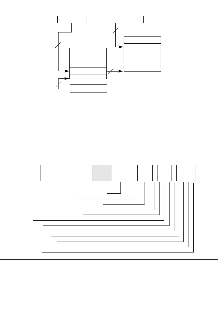
3-38 Vol. 3A
PROTECTED-MODE MEMORY MANAGEMENT
Figure 3-23 shows the format for the page-directory entries when 4-MByte pages and 36-bit
physical addresses are being used. Section 3.7.6, “Page-Directory and Page-Table Entries”
describes the functions of the flags and fields in bits 0 through 11.
Figure 3-22. Linear Address Translation (4-MByte Pages)
Figure 3-23. Format of Page-Directory Entries for 4-MByte Pages and
36-Bit Physical Addresses
0
Directory Offset
Page Directory
Directory Entry
CR3 (PDBR)
4-MByte Page
Physical Address
31 2122
Linear Address
1024 PDE = 1024 Pages
10
22
32*
*32 bits aligned onto a 4-KByte boundary.
14
31
Available for system programmer’s use
Global page
Page size (must be set to 1)
Dirty
12 11 9876543210
P
S
P
CAD
Accessed
Cache disabled
Write-through
User/Supervisor
Read/Write
Present
DP
P
W
T
U
/
S
R
/
W
GAvail.
Page Base Address
Page-Directory Entry (4-MByte Page)
22 21
Reserved
13
16
(Bits 22 Through 31)
Page Base Address (Bits 32 Through 35)
Page Attribute Table Index
17
P
A
T

Vol. 3A 3-39
PROTECTED-MODE MEMORY MANAGEMENT
3.10 PAE-ENABLED PAGING IN IA-32E MODE
Intel EM64T 64-bit extensions expand physical address extension (PAE) paging structures to
potentially support mapping a 64-bit linear address to a 52-bit physical address. In the first
implementation of Intel EM64T, PAE paging structures support translation of a 48-bit linear
address into a 40-bit physical address.
When IA-32e mode is enabled, linear address to physical address translation is different than in
PAE-enabled protected mode. Address translation from a linear address to a physical address
uses up to four levels of paging data structures. A new page mapping table, the page map level
4 table (PML4 table), is added on top of the page director pointer table.
Prior to activating IA-32e mode, PAE must be enabled by setting CR4.PAE = 1. PAE expands
the size of page-directory entries (PDE) and page-table entries (PTE) from 32 bits to 64 bits.
This change is made to support physical-address sizes of greater than 32 bits. An attempt to acti-
vate IA-32e mode prior to enabling PAE results in a general-protection exception, #GP.
PML4 tables are used in page translation only in IA-32e mode. They are not used when IA-32e
mode is disabled, whether or not PAE is enabled. The existing page-directory pointer table is
expanded to 512 eight-byte entries from four entries. As a result, nine bits of the linear address
are used to index into a PDP table rather than two bits. The size of the page-directory entry
(PDE) table and page-table entry (PTE) table remains 512 eight-byte entries, each indexed by
nine linear-address bits. The total of linear-address index bits into the collection of paging data
structures (PML4 + PDP + PDE + PTE + page offset) becomes 48. The method for translating
the high-order 16 linear-address bits into a physical address is currently reserved.
The PS flag in the page directory entry (PDE.PS) selects between 4-KByte and 2-MByte page
sizes. Because PDE.PS is used to control large page selection, the CR4.PSE bit is ignored.
3.10.1 IA-32e Mode Linear Address Translation (4-KByte Pages)
Figure 3-24 shows the PML4, page-directory-pointer, page-directory, and page-table hierarchy
when mapping linear addresses to 4-KByte pages in IA-32e mode. This paging method can be
used to address up to 236 pages, which spans a linear address space of 248 bytes.
To select the various table entries, linear addresses are divided into five sections:
•PML4-table entry — Bits 47:39 provide an offset to an entry in the PML4 table. The
selected entry provides the base physical address of a page directory pointer table.
•Page-directory-pointer-table entry — Bits 38:30 provide an offset to an entry in the
page-directory-pointer table. The selected entry provides the base physical address of a
page directory table.
•Page-directory entry — Bits 29:21 provide an offset to an entry in the selected page
directory. The selected entry provides the base physical address of a page table.
•Page-table entry — Bits 20:12 provide an offset to an entry in the selected page table.
This entry provides the base physical address of a page in physical memory.
•Page offset — Bits 11:0 provide an offset to a physical address in the page.
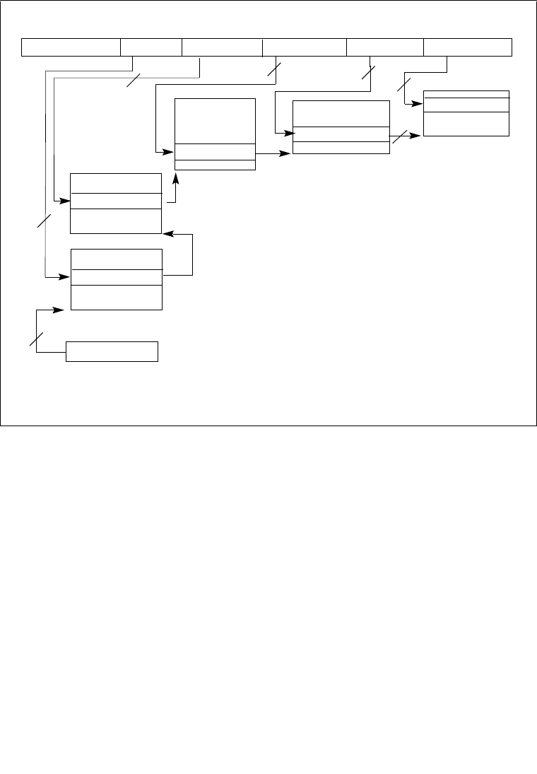
3-40 Vol. 3A
PROTECTED-MODE MEMORY MANAGEMENT
3.10.2 IA-32e Mode Linear Address Translation (2-MByte Pages)
Figure 3-25 shows the PML4 table, page-directory-pointer, and page-directory hierarchy when
mapping linear addresses to 2-MByte pages in IA-32e mode. This method can be used to address
up to 227 pages, which spans a linear address space of 248 bytes.
The 2-MByte page size is selected by setting the page size (PS) flag in a page-directory entry
(see Figure 3-14). The PSE flag in control register CR4 has no affect on the page size when PAE
is enabled. With the PS flag set, a linear address is divided into four sections:
•PML4-table entry — Bits 47:39 provide an offset to an entry in the PML4 table. The
selected entry provides the base physical address of a page directory pointer table.
•Page-directory-pointer-table entry — Bits 38:30 provide an offset to an entry in the
page-directory-pointer table. The selected entry provides the base physical address of a
page directory.
Figure 3-24. IA-32e Mode Paging Structures (4-KByte Pages)
Directory Ptr
Page-Table Entry
Linear Address
Page Table
Dir. Pointer Entry
CR3 (PML4)
39 38
Pointer Table
512 PML4 *512 PDPTE ∗ 512 PDE ∗ 512 PTE = 236 Pages
99
401
12
9
1. 40 bits aligned onto a 4-KByte boundary
28
4-KByte Page
Offset
Physical Addr
Directory Entry
Table
011122021
Directory
30 29
Page-Directory-
Page-Directory
PML4
474863
Sign Extended
9
PML4 Entry
NOTES:
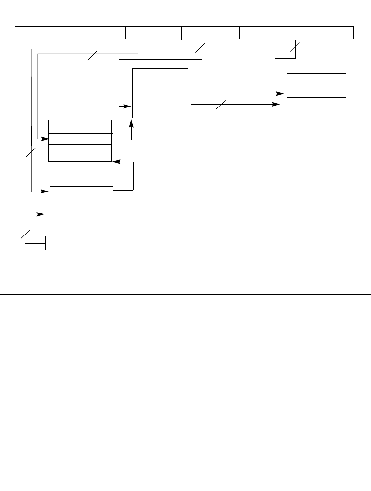
Vol. 3A 3-41
PROTECTED-MODE MEMORY MANAGEMENT
•Page-directory entry — Bits 29:21 provide an offset to an entry in the page directory. The
selected entry provides the base physical address of a 2-MByte page.
•Page offset — Bits 20:0 provides an offset to a physical address in the page.
3.10.3 Enhanced Paging Data Structures
Figure 3-26 shows the format for the PML4 table, page-directory-pointer table, page-direc-
tory and page-table entries when 4-KByte pages are used in IA-32e mode. Figure 3-27
shows the format for the PML4 table, the page-directory-pointer table and page-directory
entries when 2-MByte pages are used in IA-32e mode.
Except for the PML4 table, these enhanced formats of page-directory-pointer table, page-
directory, and page-table entries are also used in enhanced legacy PAE-enabled paging on
processors that supports Intel EM64T (see Section 3.8.1, “Enhanced Legacy PAE Paging”).
Figure 3-25. IA-32e Mode Paging Structures (2-MByte pages)
Directory Ptr
Linear Address
Dir. Pointer Entry
CR3 (PML4)
39 38
Pointer Table
512 PML4 *512 PDPTE ∗ 512 PDE = 227 Pages
99
401
21
1. 40 bits aligned onto a 4-KByte boundary
19
2-MByte Page
Offset
Physical Addr
Directory Entry
02021
Directory
30 29
Page-Directory-
Page-Directory
PML4
474863
Sign Extended
9
PML4 Entry
NOTE:
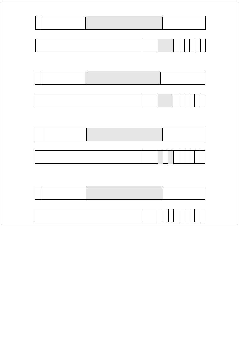
3-42 Vol. 3A
PROTECTED-MODE MEMORY MANAGEMENT
Except for bit 63, functions of the flags in these entries are as described in Section 3.7.6, “Page-
Directory and Page-Table Entries”. The differences are:
•A PML4 table entry and a page-directory-pointer-table entry are added.
•Entries are increased from 32 bits to 64 bits.
•The maximum number of entries in a page directory, page table, or PML4 table is 512.
•The P, R/W, U/S, PWT, PCD, and A flags are implemented uniformly across all four
levels.
Figure 3-26. Format of Paging Structure Entries for 4-KByte Pages in IA-32e Mode
63 32
Base
Reserved (set to 0)
Page-Directory-Pointer-Table Entry
31 12 11 9854320
P
C
D
P
W
T
Avail
Page-Directory Base Address
Addr.
Rsvd
63 32
Base
Reserved (set to 0)
Page-Directory Entry (4-KByte Page Table)
31 12 11 9876543210
P
C
0DP
P
W
T
Page-Table Base Address
Addr.
00 A R
/
W
U
/
S
63 32
Base
Reserved (set to 0)
Page-Table Entry (4-KByte Page)
31 12 11 9876543210
P
C
DDP
P
W
T
Page Base Address
Addr.
GA R
/
W
U
/
S
Avail
Avail
P
1
P
A
T
63 32
Base
Reserved (set to 0)
Page-Map-Level-4-Table Entry
31 12 11 9854320
P
C
D
P
W
T
Avail
PML4 Base Address
Addr.
Rsvd.
P
1
3962
Avail
E
X
B
51
3962
Avail
E
X
B
51
3962
Avail
E
X
B
51
R
/
W
U
/
S
3962
Avail
E
X
B
51
6
A
6
AR
/
W
U
/
S
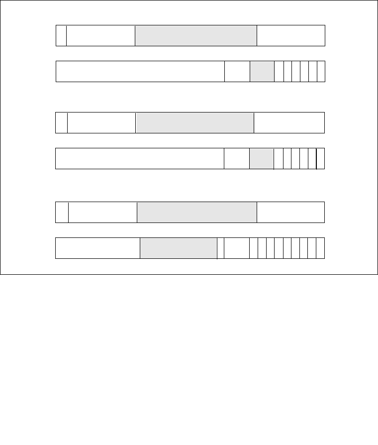
Vol. 3A 3-43
PROTECTED-MODE MEMORY MANAGEMENT
•The base physical address field in each entry is extended to 28 bits if the processor’s
implementation supports a 40-bit physical address.
•Bits 62:52 are available for use by system programmers.
•Bit 63 is the execute-disable bit if the execute-disable bit feature is supported in the
processor. If the feature is not supported, bit 63 is reserved. The functionality of the
execute disable bit is described in Section 4.11, “Page-Level Protection”. It requires both
PAE and enhanced paging data structures. Note that the execute disable bit can provide
page protection in 32-bit PAE mode and IA-32e mode.
3.10.3.1 Reserved Bit Checking
On processors supporting Intel EM64T and/or supporting the execute disable bit, the processor
will enforce reserved bit checking on paging mode specific bits.
Table 3-4 shows the reserved bits that are checked on IA-32 processors that support Intel
EM64T and when execute disable bit is either disabled or not supported. The 32-bit mode
behavior in Table 3-4 also applies to IA-32 processors that the support execute-disable bit but
not Intel EM64T.
Figure 3-27. Format of Paging Structure Entries for 2-MByte Pages in IA-32e Mode
63 62 32
Base
Reserved (set to 0)
Page-Directory-Pointer-Table Entry
31 12 11 9 854320
P
C
D
P
W
T
Avail
Page-Directory Base Address
Addr.
Rsvd
63 62 52
32
Page Base
Reserved (set to 0)
Page-Directory Entry (2-MByte Page)
31 21 20 13 12 11 9 8 7 6 5 4 3 2 1 0
P
C
DP
P
W
T
Page Base Address
G1 A R
/
W
U
/
S
Avail
P
1
63 62 32
Base
Reserved (set to 0)
Page-Map-Level-4-Table Entry
31 12 11 9854320
P
C
D
P
W
T
Avail
PML4 Base Address
Addr.
Rsvd.
P
1
39
Avail
E
X
B
51
39
Avail
E
X
B
51
R
/
W
U
/
S
39
Avail
E
X
B
51
6
A
6
AR
/
W
U
/
S
Addr,
P
A
T
Reserved (set to 0)
D

3-44 Vol. 3A
PROTECTED-MODE MEMORY MANAGEMENT
If the execute disable bit is enabled in an IA-32 processor, the reserved bits in paging data struc-
tures for legacy 32-bit mode and 64-bit mode are shown in Table 3-5.
Table 3-4. Reserved Bit Checking When Execute Disable Bit is Disabled
Mode Paging Mode Paging Structure Check Bits
32-bit 4-KByte pages (PAE = 0, PSE = 0) PDE and PT No reserved bits checked
4-MByte page (PAE = 0, PSE = 1) PDE Bit [21]
4-KByte page (PAE = 0, PSE = 1) PDE No reserved bits checked
4-KByte and 4-MByte page (PAE =
0, PSE = 1) PTE No reserved bits checked
4-KByte and 2-MByte pages (PAE
= 1, PSE = x) PDP table entry Bits [63:40] & [8:5] & [2:1]
2-MByte page (PAE = 1, PSE = x) PDE Bits [63:40] & [20:13]
4-KByte pages (PAE =1, PSE = x) PDE Bits [63:40]
4-KByte and 2-MByte pages (PAE
= 1, PSE = x) PTE Bits [63:40]
64-bit 4-KByte and 2-MByte pages (PAE
= 1, PSE = x) PML4E Bit [63], bits [51:40]
4-KByte and 2-MByte pages (PAE
= 1, PSE = x) PDPTE Bit [63], bits [51:40]
2-MByte page (PAE =1, PSE = x) PDE, 2-MByte page Bit [63], bits [51:40] & [20:13]
4-KByte pages (PAE = 1, PSE = x) PDE, 4-KByte page Bit [63], bits [51:40]
4-KByte and 2-MByte pages (PAE
= 1, PSE = x) PTE Bit [63], bits [51:40]
Table 3-5. Reserved Bit Checking When Execute Disable Bit is Enabled
Mode Paging Mode Paging Structure Check Bits
32-bit 4-KByte pages (PAE = 0, PSE =
0) PDE and PT No reserved bits checked
4-MByte page (PAE = 0, PSE = 1) PDE Bit [21]
4-KByte page (PAE = 0, PSE = 1) PDE No reserved bits checked
4-KByte and 4-MByte page (PAE =
0, PSE = 1) PTE No reserved bits checked
4-KByte and 2-MByte pages (PAE
= 1, PSE = x) PDP table entry Bits [63:40] & [8:5] & [2:1]
2-MByte page (PAE = 1, PSE = x) PDE Bits [63:40] & [20:13]
4-KByte pages (PAE = 1, PSE = x) PDE Bits [63:40]
4-KByte and 2-MByte pages (PAE
= 1, PSE = x) PTE Bits [63:40]

Vol. 3A 3-45
PROTECTED-MODE MEMORY MANAGEMENT
3.11 MAPPING SEGMENTS TO PAGES
The segmentation and paging mechanisms provide in the IA-32 architecture support a wide
variety of approaches to memory management. When segmentation and paging is combined,
segments can be mapped to pages in several ways. To implement a flat (unsegmented)
addressing environment, for example, all the code, data, and stack modules can be mapped to
one or more large segments (up to 4-GBytes) that share same range of linear addresses (see
Figure 3-2). Here, segments are essentially invisible to applications and the operating-system or
executive. If paging is used, the paging mechanism can map a single linear address space
(contained in a single segment) into virtual memory. Or, each program (or task) can have its own
large linear address space (contained in its own segment), which is mapped into virtual memory
through its own page directory and set of page tables.
Segments can be smaller than the size of a page. If one of these segments is placed in a page
which is not shared with another segment, the extra memory is wasted. For example, a small data
structure, such as a 1-byte semaphore, occupies 4K bytes if it is placed in a page by itself. If
many semaphores are used, it is more efficient to pack them into a single page.
The IA-32 architecture does not enforce correspondence between the boundaries of pages and
segments. A page can contain the end of one segment and the beginning of another. Likewise, a
segment can contain the end of one page and the beginning of another.
Memory-management software may be simpler and more efficient if it enforces some alignment
between page and segment boundaries. For example, if a segment which can fit in one page is
placed in two pages, there may be twice as much paging overhead to support access to that
segment.
One approach to combining paging and segmentation that simplifies memory-management soft-
ware is to give each segment its own page table, as shown in Figure 3-28. This convention gives
the segment a single entry in the page directory which provides the access control information
for paging the entire segment.
64-bit 4-KByte and 2-MByte pages (PAE
= 1, PSE = x) PML4E Bit [63], bits [51:40]
4-KByte and 2-MByte pages (PAE
= 1, PSE = x) PDPTE Bit [63], bits [51:40]
2-MByte page (PAE = 1, PSE = x) PDE, 2-MByte page Bit [63], bits [51:40] & [20:13]
4-KByte pages (PAE = 1, PSE = x) PDE, 4-KByte page Bit [63], bits [51:40]
4-KByte and 2-MByte pages (PAE
= 1, PSE = x) PTE Bit [63], bits [51:40]
NOTE:
x = Bit does not impact behavior.
Table 3-5. Reserved Bit Checking When Execute Disable Bit is Enabled (Contd.)
Mode Paging Mode Paging Structure Check Bits
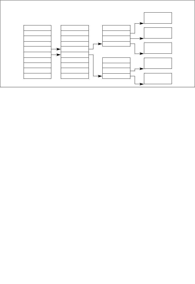
3-46 Vol. 3A
PROTECTED-MODE MEMORY MANAGEMENT
3.12 TRANSLATION LOOKASIDE BUFFERS (TLBS)
The processor stores the most recently used page-directory and page-table entries in on-chip
caches called translation lookaside buffers or TLBs. The P6 family and Pentium processors have
separate TLBs for the data and instruction caches. Also, the P6 family processors maintain sepa-
rate TLBs for 4-KByte and 4-MByte page sizes. The CPUID instruction can be used to deter-
mine the sizes of the TLBs provided in the P6 family and Pentium processors.
Most paging is performed using the contents of the TLBs. Bus cycles to the page directory and
page tables in memory are performed only when the TLBs do not contain the translation infor-
mation for a requested page.
The TLBs are inaccessible to application programs and tasks (privilege level greater than 0); that
is, they cannot invalidate TLBs. Only, operating system or executive procedures running at priv-
ilege level of 0 can invalidate TLBs or selected TLB entries. Whenever a page-directory or
page-table entry is changed (including when the present flag is set to zero), the operating-system
must immediately invalidate the corresponding entry in the TLB so that it can be updated the
next time the entry is referenced.
All of the (non-global) TLBs are automatically invalidated any time the CR3 register is loaded
(unless the G flag for a page or page-table entry is set, as describe later in this section). The CR3
register can be loaded in either of two ways:
•Explicitly, using the MOV instruction, for example:
MOV CR3, EAX
where the EAX register contains an appropriate page-directory base address.
Figure 3-28. Memory Management Convention That Assigns a Page Table
to Each Segment
Seg. Descript.
LDT
Seg. Descript.
PDE
Page Directory
PDE
PTE
PTE
PTE
PTE
PTE
Page s
Page Frames

Vol. 3A 3-47
PROTECTED-MODE MEMORY MANAGEMENT
•Implicitly by executing a task switch, which automatically changes the contents of the CR3
register.
The INVLPG instruction is provided to invalidate a specific page-table entry in the TLB.
Normally, this instruction invalidates only an individual TLB entry; however, in some cases, it
may invalidate more than the selected entry and may even invalidate all of the TLBs. This
instruction ignores the setting of the G flag in a page-directory or page-table entry (see following
paragraph).
(Introduced in the Pentium Pro processor.) The page global enable (PGE) flag in register CR4
and the global (G) flag of a page-directory or page-table entry (bit 8) can be used to prevent
frequently used pages from being automatically invalidated in the TLBs on a task switch or a
load of register CR3. (See Section 3.7.6, “Page-Directory and Page-Table Entries”, for more
information about the global flag.) When the processor loads a page-directory or page-table
entry for a global page into a TLB, the entry will remain in the TLB indefinitely. The only ways
to deterministically invalidate global page entries are as follows:
•Clear the PGE flag; this will invalidate the TLBs.
•Execute the INVLPG instruction to invalidate individual page-directory or page-table
entries in the TLBs.
For additional information about invalidation of the TLBs, see Section 10.9, “Invalidating the
Translation Lookaside Buffers (TLBs)”.

3-48 Vol. 3A
PROTECTED-MODE MEMORY MANAGEMENT

4
Protection

Vol. 3A 4-1
CHAPTER 4
PROTECTION
In protected mode, the IA-32 architecture provides a protection mechanism that operates at both
the segment level and the page level. This protection mechanism provides the ability to limit
access to certain segments or pages based on privilege levels (four privilege levels for segments
and two privilege levels for pages). For example, critical operating-system code and data can be
protected by placing them in more privileged segments than those that contain applications
code. The processor’s protection mechanism will then prevent application code from accessing
the operating-system code and data in any but a controlled, defined manner.
Segment and page protection can be used at all stages of software development to assist in local-
izing and detecting design problems and bugs. It can also be incorporated into end-products to
offer added robustness to operating systems, utilities software, and applications software.
When the protection mechanism is used, each memory reference is checked to verify that it
satisfies various protection checks. All checks are made before the memory cycle is started; any
violation results in an exception. Because checks are performed in parallel with address transla-
tion, there is no performance penalty. The protection checks that are performed fall into the
following categories:
•Limit checks.
•Type checks.
•Privilege level checks.
•Restriction of addressable domain.
•Restriction of procedure entry-points.
•Restriction of instruction set.
All protection violation results in an exception being generated. See Chapter 5, “Interrupt and
Exception Handling,” for an explanation of the exception mechanism. This chapter describes the
protection mechanism and the violations which lead to exceptions.
The following sections describe the protection mechanism available in protected mode. See
Chapter 15, “8086 Emulation,” for information on protection in real-address and virtual-8086
mode.
4.1 ENABLING AND DISABLING SEGMENT AND PAGE
PROTECTION
Setting the PE flag in register CR0 causes the processor to switch to protected mode, which in
turn enables the segment-protection mechanism. Once in protected mode, there is no control bit
for turning the protection mechanism on or off. The part of the segment-protection mechanism

4-2 Vol. 3A
PROTECTION
that is based on privilege levels can essentially be disabled while still in protected mode by
assigning a privilege level of 0 (most privileged) to all segment selectors and segment descrip-
tors. This action disables the privilege level protection barriers between segments, but other
protection checks such as limit checking and type checking are still carried out.
Page-level protection is automatically enabled when paging is enabled (by setting the PG flag
in register CR0). Here again there is no mode bit for turning off page-level protection once
paging is enabled. However, page-level protection can be disabled by performing the following
operations:
•Clear the WP flag in control register CR0.
•Set the read/write (R/W) and user/supervisor (U/S) flags for each page-directory and page-
table entry.
This action makes each page a writable, user page, which in effect disables page-level
protection.
4.2 FIELDS AND FLAGS USED FOR SEGMENT-LEVEL AND
PAGE-LEVEL PROTECTION
The processor’s protection mechanism uses the following fields and flags in the system data
structures to control access to segments and pages:
•Descriptor type (S) flag — (Bit 12 in the second doubleword of a segment descriptor.)
Determines if the segment descriptor is for a system segment or a code or data segment.
•Type field — (Bits 8 through 11 in the second doubleword of a segment descriptor.)
Determines the type of code, data, or system segment.
•Limit field — (Bits 0 through 15 of the first doubleword and bits 16 through 19 of the
second doubleword of a segment descriptor.) Determines the size of the segment, along
with the G flag and E flag (for data segments).
•G flag — (Bit 23 in the second doubleword of a segment descriptor.) Determines the size
of the segment, along with the limit field and E flag (for data segments).
•E flag — (Bit 10 in the second doubleword of a data-segment descriptor.) Determines the
size of the segment, along with the limit field and G flag.
•Descriptor privilege level (DPL) field — (Bits 13 and 14 in the second doubleword of a
segment descriptor.) Determines the privilege level of the segment.
•Requested privilege level (RPL) field — (Bits 0 and 1 of any segment selector.) Specifies
the requested privilege level of a segment selector.
•Current privilege level (CPL) field — (Bits 0 and 1 of the CS segment register.) Indicates
the privilege level of the currently executing program or procedure. The term current
privilege level (CPL) refers to the setting of this field.
•User/supervisor (U/S) flag — (Bit 2 of a page-directory or page-table entry.) Determines
the type of page: user or supervisor.
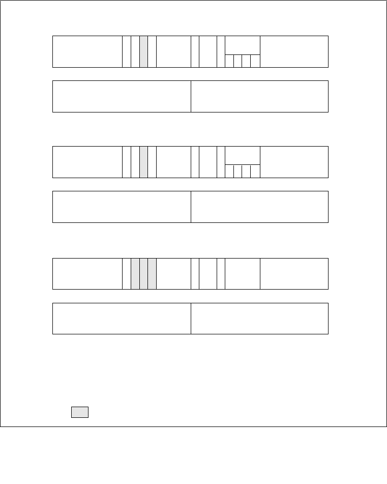
Vol. 3A 4-3
PROTECTION
•Read/write (R/W) flag — (Bit 1 of a page-directory or page-table entry.) Determines the
type of access allowed to a page: read only or read-write.
Figure 4-1 shows the location of the various fields and flags in the data, code, and system-
segment descriptors; Figure 3-6 shows the location of the RPL (or CPL) field in a segment
selector (or the CS register); and Figure 3-14 shows the location of the U/S and R/W flags in the
page-directory and page-table entries.
Figure 4-1. Descriptor Fields Used for Protection
Base 23:16
31 24 23 22 21 20 19 16 15 13
14 12 11 870
P
Base 31:24 GD
P
L
Type
1
04
31 16 15 0
Base Address 15:00 Segment Limit 15:00 0
Base 23:16
A
V
L
Limit
19:16
B
AWE0
Data-Segment Descriptor
31 24 23 22 21 20 19 16 15 13
14 12 11 870
P
Base 31:24 GD
P
L
Type
1
04
31 16 15 0
Base Address 15:00 Segment Limit 15:00 0
Base 23:16
A
V
L
Limit
19:16
D
ARC1
Code-Segment Descriptor
31 24 23 22 21 20 19 16 15 13
14 12 11 87 0
P
Base 31:24 GD
P
LType
04
31 16 15 0
Base Address 15:00 Segment Limit 15:00 0
Limit
19:16
System-Segment Descriptor
A
B
C
D
DPL
Accessed
Big
Conforming
Default
Descriptor Privilege Level
Reserved
E
G
R
LIMIT
W
P
Expansion Direction
Granularity
Readable
Segment Limit
Writable
Present
0
AVL Available to Sys. Programmer’s

4-4 Vol. 3A
PROTECTION
Many different styles of protection schemes can be implemented with these fields and flags.
When the operating system creates a descriptor, it places values in these fields and flags in
keeping with the particular protection style chosen for an operating system or executive. Appli-
cation program do not generally access or modify these fields and flags.
The following sections describe how the processor uses these fields and flags to perform the
various categories of checks described in the introduction to this chapter.
4.2.1 Code Segment Descriptor in 64-bit Mode
Code segments continue to exist in 64-bit mode even though, for address calculations, the
segment base is treated as zero. Some code-segment (CS) descriptor content (the base address
and limit fields) is ignored; the remaining fields function normally (except for the readable bit
in the type field).
Code segment descriptors and selectors are needed in IA-32e mode to establish the processor’s
operating mode and execution privilege-level. The usage is as follows:
•IA-32e mode uses a previously unused bit in the CS descriptor. Bit 53 is defined as the
64-bit (L) flag and is used to select between 64-bit mode and compatibility mode when
IA-32e mode is active (IA32_EFER.LMA = 1). See Figure 4-2.
— If CS.L = 0 and IA-32e mode is active, the processor is running in compatibility mode.
In this case, CS.D selects the default size for data and addresses. If CS.D = 0, the
default data and address size is 16 bits. If CS.D = 1, the default data and address size is
32 bits.
— If CS.L = 1 and IA-32e mode is active, the only valid setting is CS.D = 0. This setting
indicates a default operand size of 32 bits and a default address size of 64 bits. The
CS.L = 1 and CS.D = 1 bit combination is reserved for future use and a #GP fault will
be generated on an attempt to use a code segment with these bits set in IA-32e mode.
•In IA-32e mode, the CS descriptor’s DPL is used for execution privilege checks (as in
legacy 32-bit mode).

Vol. 3A 4-5
PROTECTION
4.3 LIMIT CHECKING
The limit field of a segment descriptor prevents programs or procedures from addressing
memory locations outside the segment. The effective value of the limit depends on the setting
of the G (granularity) flag (see Figure 4-1). For data segments, the limit also depends on the
E (expansion direction) flag and the B (default stack pointer size and/or upper bound) flag. The
E flag is one of the bits in the type field when the segment descriptor is for a data-segment type.
When the G flag is clear (byte granularity), the effective limit is the value of the 20-bit limit field
in the segment descriptor. Here, the limit ranges from 0 to FFFFFH (1 MByte). When the G flag
is set (4-KByte page granularity), the processor scales the value in the limit field by a factor of
212 (4 KBytes). In this case, the effective limit ranges from FFFH (4 KBytes) to FFFFFFFFH
(4 GBytes). Note that when scaling is used (G flag is set), the lower 12 bits of a segment offset
(address) are not checked against the limit; for example, note that if the segment limit is 0,
offsets 0 through FFFH are still valid.
For all types of segments except expand-down data segments, the effective limit is the last
address that is allowed to be accessed in the segment, which is one less than the size, in bytes,
of the segment. The processor causes a general-protection exception any time an attempt is made
to access the following addresses in a segment:
•A byte at an offset greater than the effective limit
•A word at an offset greater than the (effective-limit – 1)
•A doubleword at an offset greater than the (effective-limit – 3)
•A quadword at an offset greater than the (effective-limit – 7)
Figure 4-2. Descriptor Fields with Flags used in IA-32e Mode
31 24 23 22 21 20 19 16 15 13
14 12 11 870
P
GD
P
L
Type
1
L4
0
0
A
V
L
D
ARC1
Code-Segment Descriptor
31
A
C
D
DPL
Accessed
Conforming
Default
Descriptor Privilege Level
G
RGranularity
Readable
AVL Available to Sys. Programmer’s
L 64-Bit Flag
P Present

4-6 Vol. 3A
PROTECTION
For expand-down data segments, the segment limit has the same function but is interpreted
differently. Here, the effective limit specifies the last address that is not allowed to be accessed
within the segment; the range of valid offsets is from (effective-limit + 1) to FFFFFFFFH if the
B flag is set and from (effective-limit + 1) to FFFFH if the B flag is clear. An expand-down
segment has maximum size when the segment limit is 0.
Limit checking catches programming errors such as runaway code, runaway subscripts, and
invalid pointer calculations. These errors are detected when they occur, so identification of the
cause is easier. Without limit checking, these errors could overwrite code or data in another
segment.
In addition to checking segment limits, the processor also checks descriptor table limits. The
GDTR and IDTR registers contain 16-bit limit values that the processor uses to prevent
programs from selecting a segment descriptors outside the respective descriptor tables. The
LDTR and task registers contain 32-bit segment limit value (read from the segment descriptors
for the current LDT and TSS, respectively). The processor uses these segment limits to prevent
accesses beyond the bounds of the current LDT and TSS. See Section 3.5.1, “Segment
Descriptor Tables,” for more information on the GDT and LDT limit fields; see Section 5.10,
“Interrupt Descriptor Table (IDT),” for more information on the IDT limit field; and see Section
6.2.4, “Task Register,” for more information on the TSS segment limit field.
4.3.1 Limit Checking in 64-bit Mode
In 64-bit mode, the processor does not perform runtime limit checking on code or data segments.
However, the processor does check descriptor-table limits.
4.4 TYPE CHECKING
Segment descriptors contain type information in two places:
•The S (descriptor type) flag.
•The type field.
The processor uses this information to detect programming errors that result in an attempt to use
a segment or gate in an incorrect or unintended manner.
The S flag indicates whether a descriptor is a system type or a code or data type. The type field
provides 4 additional bits for use in defining various types of code, data, and system descriptors.
Table 3-1 shows the encoding of the type field for code and data descriptors; Table 3-2 shows
the encoding of the field for system descriptors.
The processor examines type information at various times while operating on segment selectors
and segment descriptors. The following list gives examples of typical operations where type
checking is performed (this list is not exhaustive):

Vol. 3A 4-7
PROTECTION
•When a segment selector is loaded into a segment register — Certain segment registers
can contain only certain descriptor types, for example:
— The CS register only can be loaded with a selector for a code segment.
— Segment selectors for code segments that are not readable or for system segments
cannot be loaded into data-segment registers (DS, ES, FS, and GS).
— Only segment selectors of writable data segments can be loaded into the SS register.
•When a segment selector is loaded into the LDTR or task register — For example:
— The LDTR can only be loaded with a selector for an LDT.
— The task register can only be loaded with a segment selector for a TSS.
•When instructions access segments whose descriptors are already loaded into
segment registers — Certain segments can be used by instructions only in certain
predefined ways, for example:
— No instruction may write into an executable segment.
— No instruction may write into a data segment if it is not writable.
— No instruction may read an executable segment unless the readable flag is set.
•When an instruction operand contains a segment selector — Certain instructions can
access segments or gates of only a particular type, for example:
— A far CALL or far JMP instruction can only access a segment descriptor for a
conforming code segment, nonconforming code segment, call gate, task gate, or TSS.
— The LLDT instruction must reference a segment descriptor for an LDT.
— The LTR instruction must reference a segment descriptor for a TSS.
— The LAR instruction must reference a segment or gate descriptor for an LDT, TSS,
call gate, task gate, code segment, or data segment.
— The LSL instruction must reference a segment descriptor for a LDT, TSS, code
segment, or data segment.
— IDT entries must be interrupt, trap, or task gates.
•During certain internal operations — For example:
— On a far call or far jump (executed with a far CALL or far JMP instruction), the
processor determines the type of control transfer to be carried out (call or jump to
another code segment, a call or jump through a gate, or a task switch) by checking the
type field in the segment (or gate) descriptor pointed to by the segment (or gate)
selector given as an operand in the CALL or JMP instruction. If the descriptor type is
for a code segment or call gate, a call or jump to another code segment is indicated; if
the descriptor type is for a TSS or task gate, a task switch is indicated.

4-8 Vol. 3A
PROTECTION
— On a call or jump through a call gate (or on an interrupt- or exception-handler call
through a trap or interrupt gate), the processor automatically checks that the segment
descriptor being pointed to by the gate is for a code segment.
— On a call or jump to a new task through a task gate (or on an interrupt- or exception-
handler call to a new task through a task gate), the processor automatically checks that
the segment descriptor being pointed to by the task gate is for a TSS.
— On a call or jump to a new task by a direct reference to a TSS, the processor automati-
cally checks that the segment descriptor being pointed to by the CALL or JMP
instruction is for a TSS.
— On return from a nested task (initiated by an IRET instruction), the processor checks
that the previous task link field in the current TSS points to a TSS.
4.4.1 Null Segment Selector Checking
Attempting to load a null segment selector (see Section 3.4.2, “Segment Selectors”) into the CS
or SS segment register generates a general-protection exception (#GP). A null segment selector
can be loaded into the DS, ES, FS, or GS register, but any attempt to access a segment through
one of these registers when it is loaded with a null segment selector results in a #GP exception
being generated. Loading unused data-segment registers with a null segment selector is a useful
method of detecting accesses to unused segment registers and/or preventing unwanted accesses
to data segments.
4.4.1.1 NULL Segment Checking in 64-bit Mode
In 64-bit mode, the processor does not perform runtime checking on NULL segment selectors.
The processor does not cause a #GP fault when an attempt is made to access memory where the
referenced segment register has a NULL segment selector.
4.5 PRIVILEGE LEVELS
The processor’s segment-protection mechanism recognizes 4 privilege levels, numbered from 0
to 3. The greater numbers mean lesser privileges. Figure 4-3 shows how these levels of privilege
can be interpreted as rings of protection.
The center (reserved for the most privileged code, data, and stacks) is used for the segments
containing the critical software, usually the kernel of an operating system. Outer rings are used
for less critical software. (Systems that use only 2 of the 4 possible privilege levels should use
levels 0 and 3.)

Vol. 3A 4-9
PROTECTION
The processor uses privilege levels to prevent a program or task operating at a lesser privilege
level from accessing a segment with a greater privilege, except under controlled situations.
When the processor detects a privilege level violation, it generates a general-protection excep-
tion (#GP).
To carry out privilege-level checks between code segments and data segments, the processor
recognizes the following three types of privilege levels:
•Current privilege level (CPL) — The CPL is the privilege level of the currently
executing program or task. It is stored in bits 0 and 1 of the CS and SS segment registers.
Normally, the CPL is equal to the privilege level of the code segment from which instruc-
tions are being fetched. The processor changes the CPL when program control is
transferred to a code segment with a different privilege level. The CPL is treated slightly
differently when accessing conforming code segments. Conforming code segments can be
accessed from any privilege level that is equal to or numerically greater (less privileged)
than the DPL of the conforming code segment. Also, the CPL is not changed when the
processor accesses a conforming code segment that has a different privilege level than the
CPL.
•Descriptor privilege level (DPL) — The DPL is the privilege level of a segment or gate.
It is stored in the DPL field of the segment or gate descriptor for the segment or gate.
When the currently executing code segment attempts to access a segment or gate, the DPL
of the segment or gate is compared to the CPL and RPL of the segment or gate selector (as
described later in this section). The DPL is interpreted differently, depending on the type of
segment or gate being accessed:
—Data segment — The DPL indicates the numerically highest privilege level that a
program or task can have to be allowed to access the segment. For example, if the DPL
of a data segment is 1, only programs running at a CPL of 0 or 1 can access the
segment.
Figure 4-3. Protection Rings
Level 0
Level 1
Level 2
Level 3
Protection Rings
Operating
Operating System
Services
System
Kernel
Applications

4-10 Vol. 3A
PROTECTION
—Nonconforming code segment (without using a call gate) — The DPL indicates the
privilege level that a program or task must be at to access the segment. For example, if
the DPL of a nonconforming code segment is 0, only programs running at a CPL of 0
can access the segment.
—Call gate — The DPL indicates the numerically highest privilege level that the
currently executing program or task can be at and still be able to access the call gate.
(This is the same access rule as for a data segment.)
—Conforming code segment and nonconforming code segment accessed through a
call gate — The DPL indicates the numerically lowest privilege level that a program
or task can have to be allowed to access the segment. For example, if the DPL of a
conforming code segment is 2, programs running at a CPL of 0 or 1 cannot access the
segment.
—TSS — The DPL indicates the numerically highest privilege level that the currently
executing program or task can be at and still be able to access the TSS. (This is the
same access rule as for a data segment.)
•Requested privilege level (RPL) — The RPL is an override privilege level that is
assigned to segment selectors. It is stored in bits 0 and 1 of the segment selector. The
processor checks the RPL along with the CPL to determine if access to a segment is
allowed. Even if the program or task requesting access to a segment has sufficient privilege
to access the segment, access is denied if the RPL is not of sufficient privilege level. That
is, if the RPL of a segment selector is numerically greater than the CPL, the RPL overrides
the CPL, and vice versa. The RPL can be used to insure that privileged code does not
access a segment on behalf of an application program unless the program itself has access
privileges for that segment. See Section 4.10.4, “Checking Caller Access Privileges
(ARPL Instruction),” for a detailed description of the purpose and typical use of the RPL.
Privilege levels are checked when the segment selector of a segment descriptor is loaded into a
segment register. The checks used for data access differ from those used for transfers of program
control among code segments; therefore, the two kinds of accesses are considered separately in
the following sections.
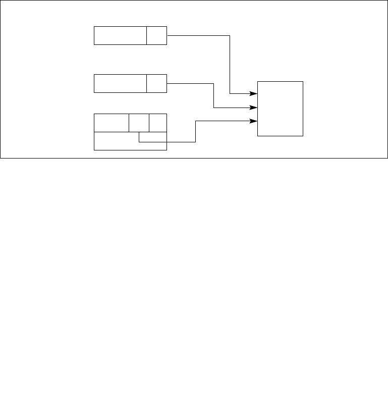
Vol. 3A 4-11
PROTECTION
4.6 PRIVILEGE LEVEL CHECKING WHEN ACCESSING DATA
SEGMENTS
To access operands in a data segment, the segment selector for the data segment must be loaded
into the data-segment registers (DS, ES, FS, or GS) or into the stack-segment register (SS).
(Segment registers can be loaded with the MOV, POP, LDS, LES, LFS, LGS, and LSS instruc-
tions.) Before the processor loads a segment selector into a segment register, it performs a priv-
ilege check (see Figure 4-4) by comparing the privilege levels of the currently running program
or task (the CPL), the RPL of the segment selector, and the DPL of the segment’s segment
descriptor. The processor loads the segment selector into the segment register if the DPL is
numerically greater than or equal to both the CPL and the RPL. Otherwise, a general-protection
fault is generated and the segment register is not loaded.
Figure 4-5 shows four procedures (located in codes segments A, B, C, and D), each running at
different privilege levels and each attempting to access the same data segment.
1. The procedure in code segment A is able to access data segment E using segment selector
E1, because the CPL of code segment A and the RPL of segment selector E1 are equal to
the DPL of data segment E.
2. The procedure in code segment B is able to access data segment E using segment selector
E2, because the CPL of code segment B and the RPL of segment selector E2 are both
numerically lower than (more privileged) than the DPL of data segment E. A code segment
B procedure can also access data segment E using segment selector E1.
3. The procedure in code segment C is not able to access data segment E using segment
selector E3 (dotted line), because the CPL of code segment C and the RPL of segment
selector E3 are both numerically greater than (less privileged) than the DPL of data
segment E. Even if a code segment C procedure were to use segment selector E1 or E2,
such that the RPL would be acceptable, it still could not access data segment E because its
CPL is not privileged enough.
Figure 4-4. Privilege Check for Data Access
CPL
RPL
DPL
Privilege
Check
Data-Segment Descriptor
CS Register
Segment Selector
For Data Segment
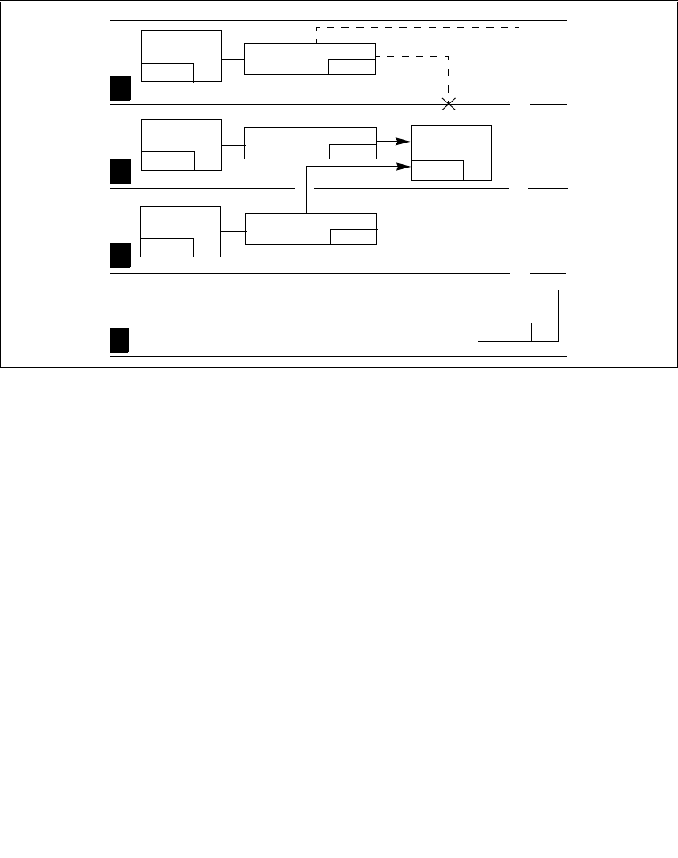
4-12 Vol. 3A
PROTECTION
4. The procedure in code segment D should be able to access data segment E because code
segment D’s CPL is numerically less than the DPL of data segment E. However, the RPL
of segment selector E3 (which the code segment D procedure is using to access data
segment E) is numerically greater than the DPL of data segment E, so access is not
allowed. If the code segment D procedure were to use segment selector E1 or E2 to access
the data segment, access would be allowed.
As demonstrated in the previous examples, the addressable domain of a program or task varies
as its CPL changes. When the CPL is 0, data segments at all privilege levels are accessible; when
the CPL is 1, only data segments at privilege levels 1 through 3 are accessible; when the CPL is
3, only data segments at privilege level 3 are accessible.
The RPL of a segment selector can always override the addressable domain of a program or task.
When properly used, RPLs can prevent problems caused by accidental (or intensional) use of
segment selectors for privileged data segments by less privileged programs or procedures.
It is important to note that the RPL of a segment selector for a data segment is under software
control. For example, an application program running at a CPL of 3 can set the RPL for a data-
segment selector to 0. With the RPL set to 0, only the CPL checks, not the RPL checks, will
provide protection against deliberate, direct attempts to violate privilege-level security for the
data segment. To prevent these types of privilege-level-check violations, a program or procedure
can check access privileges whenever it receives a data-segment selector from another proce-
dure (see Section 4.10.4, “Checking Caller Access Privileges (ARPL Instruction)”).
Figure 4-5. Examples of Accessing Data Segments From Various Privilege Levels
Data
Lowest Privilege
Highest Privilege
Segment E
3
2
1
0
CPL=1
CPL=3
CPL=0
DPL=2
CPL=2
Segment Sel. E3
RPL=3
Segment Sel. E1
RPL=2
Segment Sel. E2
RPL=1
Code
Segment C
Code
Segment A
Code
Segment B
Code
Segment D

Vol. 3A 4-13
PROTECTION
4.6.1 Accessing Data in Code Segments
In some instances it may be desirable to access data structures that are contained in a code
segment. The following methods of accessing data in code segments are possible:
•Load a data-segment register with a segment selector for a nonconforming, readable, code
segment.
•Load a data-segment register with a segment selector for a conforming, readable, code
segment.
•Use a code-segment override prefix (CS) to read a readable, code segment whose selector
is already loaded in the CS register.
The same rules for accessing data segments apply to method 1. Method 2 is always valid because
the privilege level of a conforming code segment is effectively the same as the CPL, regardless
of its DPL. Method 3 is always valid because the DPL of the code segment selected by the CS
register is the same as the CPL.
4.7 PRIVILEGE LEVEL CHECKING WHEN LOADING THE SS
REGISTER
Privilege level checking also occurs when the SS register is loaded with the segment selector for
a stack segment. Here all privilege levels related to the stack segment must match the CPL; that
is, the CPL, the RPL of the stack-segment selector, and the DPL of the stack-segment descriptor
must be the same. If the RPL and DPL are not equal to the CPL, a general-protection exception
(#GP) is generated.
4.8 PRIVILEGE LEVEL CHECKING WHEN TRANSFERRING
PROGRAM CONTROL BETWEEN CODE SEGMENTS
To transfer program control from one code segment to another, the segment selector for the
destination code segment must be loaded into the code-segment register (CS). As part of this
loading process, the processor examines the segment descriptor for the destination code segment
and performs various limit, type, and privilege checks. If these checks are successful, the CS
register is loaded, program control is transferred to the new code segment, and program execu-
tion begins at the instruction pointed to by the EIP register.
Program control transfers are carried out with the JMP, CALL, RET, SYSENTER, SYSEXIT,
INT n, and IRET instructions, as well as by the exception and interrupt mechanisms. Exceptions,
interrupts, and the IRET instruction are special cases discussed in Chapter 5, “Interrupt and
Exception Handling.” This chapter discusses only the JMP, CALL, RET, SYSENTER, and
SYSEXIT instructions.
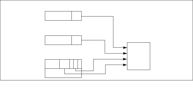
4-14 Vol. 3A
PROTECTION
A JMP or CALL instruction can reference another code segment in any of four ways:
•The target operand contains the segment selector for the target code segment.
•The target operand points to a call-gate descriptor, which contains the segment selector for
the target code segment.
•The target operand points to a TSS, which contains the segment selector for the target code
segment.
•The target operand points to a task gate, which points to a TSS, which in turn contains the
segment selector for the target code segment.
The following sections describe first two types of references. See Section 6.3, “Task Switching,”
for information on transferring program control through a task gate and/or TSS.
The SYSENTER and SYSEXIT instructions are special instructions for making fast calls to and
returns from operating system or executive procedures. These instructions are discussed briefly
in Section 4.8.7, “Performing Fast Calls to System Procedures with the SYSENTER and
SYSEXIT Instructions.”
4.8.1 Direct Calls or Jumps to Code Segments
The near forms of the JMP, CALL, and RET instructions transfer program control within the
current code segment, so privilege-level checks are not performed. The far forms of the JMP,
CALL, and RET instructions transfer control to other code segments, so the processor does
perform privilege-level checks.
When transferring program control to another code segment without going through a call gate,
the processor examines four kinds of privilege level and type information (see Figure 4-6):
•The CPL. (Here, the CPL is the privilege level of the calling code segment; that is, the code
segment that contains the procedure that is making the call or jump.)
Figure 4-6. Privilege Check for Control Transfer Without Using a Gate
CPL
RPL
DPL
Privilege
Check
CS Register
Segment Selector
For Code Segment
Destination Code
Segment Descriptor
C

Vol. 3A 4-15
PROTECTION
•The DPL of the segment descriptor for the destination code segment that contains the
called procedure.
•The RPL of the segment selector of the destination code segment.
•The conforming (C) flag in the segment descriptor for the destination code segment, which
determines whether the segment is a conforming (C flag is set) or nonconforming (C flag is
clear) code segment. See Section 3.4.5.1, “Code- and Data-Segment Descriptor Types,” for
more information about this flag.
The rules that the processor uses to check the CPL, RPL, and DPL depends on the setting of the
C flag, as described in the following sections.
4.8.1.1 Accessing Nonconforming Code Segments
When accessing nonconforming code segments, the CPL of the calling procedure must be equal
to the DPL of the destination code segment; otherwise, the processor generates a general-protec-
tion exception (#GP). For example in Figure 4-7:
•Code segment C is a nonconforming code segment. A procedure in code segment A can
call a procedure in code segment C (using segment selector C1) because they are at the
same privilege level (CPL of code segment A is equal to the DPL of code segment C).
•A procedure in code segment B cannot call a procedure in code segment C (using segment
selector C2 or C1) because the two code segments are at different privilege levels.
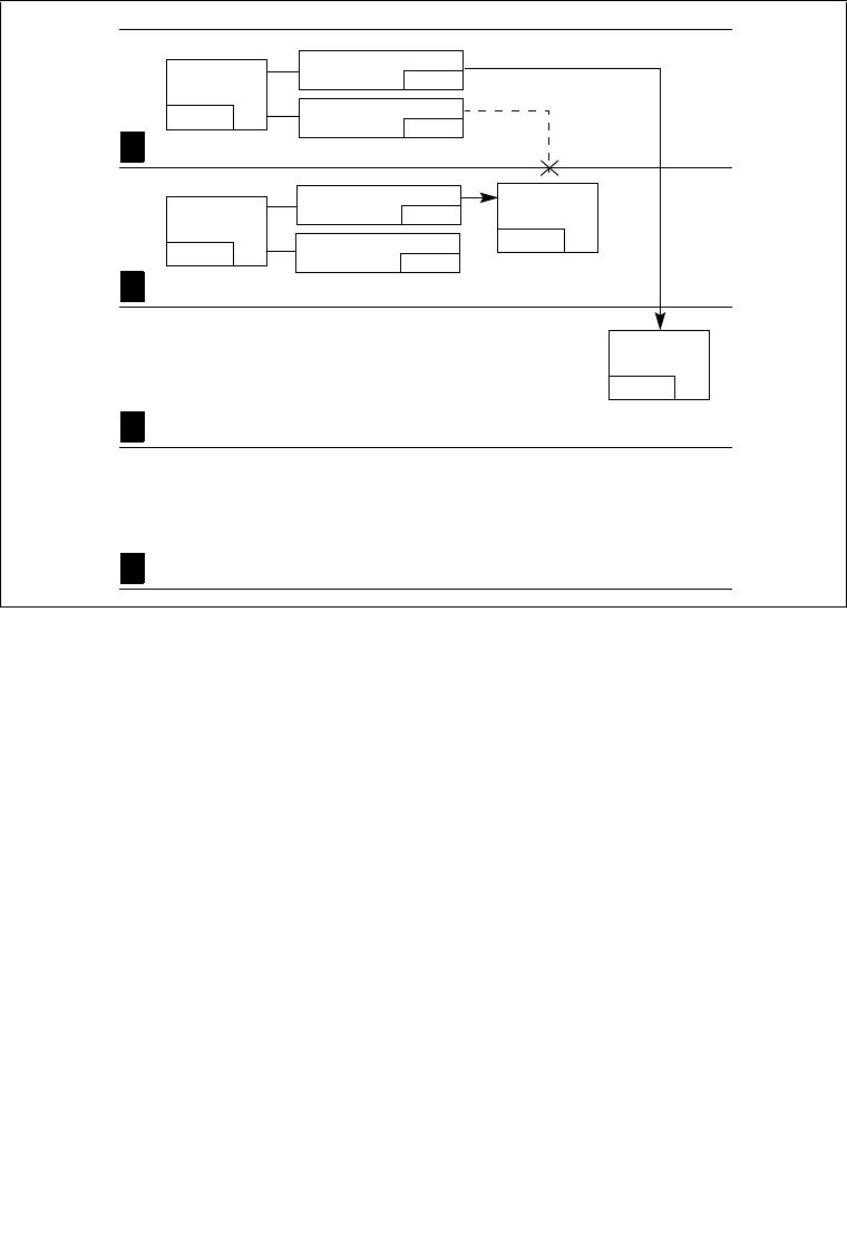
4-16 Vol. 3A
PROTECTION
The RPL of the segment selector that points to a nonconforming code segment has a limited
effect on the privilege check. The RPL must be numerically less than or equal to the CPL of the
calling procedure for a successful control transfer to occur. So, in the example in Figure 4-7, the
RPLs of segment selectors C1 and C2 could legally be set to 0, 1, or 2, but not to 3.
When the segment selector of a nonconforming code segment is loaded into the CS register, the
privilege level field is not changed; that is, it remains at the CPL (which is the privilege level of
the calling procedure). This is true, even if the RPL of the segment selector is different from the
CPL.
4.8.1.2 Accessing Conforming Code Segments
When accessing conforming code segments, the CPL of the calling procedure may be numeri-
cally equal to or greater than (less privileged) the DPL of the destination code segment; the
processor generates a general-protection exception (#GP) only if the CPL is less than the DPL.
(The segment selector RPL for the destination code segment is not checked if the segment is a
conforming code segment.)
Figure 4-7. Examples of Accessing Conforming and Nonconforming Code Segments
From Various Privilege Levels
Code
Segment D
Code
Segment C
Code
Segment A
Lowest Privilege
Highest Privilege
CPL=3
Code
Segment B
Nonconforming
Code Segment
Conforming
Code Segment
3
2
1
0
CPL=2 DPL=2
DPL=1
Segment Sel. D1
RPL=2
Segment Sel. D2
RPL=3
Segment Sel. C2
RPL=3
Segment Sel. C1
RPL=2

Vol. 3A 4-17
PROTECTION
In the example in Figure 4-7, code segment D is a conforming code segment. Therefore, calling
procedures in both code segment A and B can access code segment D (using either segment
selector D1 or D2, respectively), because they both have CPLs that are greater than or equal to
the DPL of the conforming code segment. For conforming code segments, the DPL repre-
sents the numerically lowest privilege level that a calling procedure may be at to success-
fully make a call to the code segment.
(Note that segments selectors D1 and D2 are identical except for their respective RPLs. But
since RPLs are not checked when accessing conforming code segments, the two segment selec-
tors are essentially interchangeable.)
When program control is transferred to a conforming code segment, the CPL does not change,
even if the DPL of the destination code segment is less than the CPL. This situation is the only
one where the CPL may be different from the DPL of the current code segment. Also, since the
CPL does not change, no stack switch occurs.
Conforming segments are used for code modules such as math libraries and exception handlers,
which support applications but do not require access to protected system facilities. These
modules are part of the operating system or executive software, but they can be executed at
numerically higher privilege levels (less privileged levels). Keeping the CPL at the level of a
calling code segment when switching to a conforming code segment prevents an application
program from accessing nonconforming code segments while at the privilege level (DPL) of a
conforming code segment and thus prevents it from accessing more privileged data.
Most code segments are nonconforming. For these segments, program control can be transferred
only to code segments at the same level of privilege, unless the transfer is carried out through a
call gate, as described in the following sections.
4.8.2 Gate Descriptors
To provide controlled access to code segments with different privilege levels, the processor
provides special set of descriptors called gate descriptors. There are four kinds of gate
descriptors:
•Call gates
•Trap gates
•Interrupt gates
•Task gates
Task gates are used for task switching and are discussed in Chapter 6, “Task Management”. Trap
and interrupt gates are special kinds of call gates used for calling exception and interrupt
handlers. The are described in Chapter 5, “Interrupt and Exception Handling.” This chapter is
concerned only with call gates.
4-18 Vol. 3A
PROTECTION
4.8.3 Call Gates
Call gates facilitate controlled transfers of program control between different privilege levels.
They are typically used only in operating systems or executives that use the privilege-level
protection mechanism. Call gates are also useful for transferring program control between 16-bit
and 32-bit code segments, as described in Section 16.4, “Transferring Control Among Mixed-
Size Code Segments.”
Figure 4-8 shows the format of a call-gate descriptor. A call-gate descriptor may reside in the
GDT or in an LDT, but not in the interrupt descriptor table (IDT). It performs six functions:
•It specifies the code segment to be accessed.
•It defines an entry point for a procedure in the specified code segment.
•It specifies the privilege level required for a caller trying to access the procedure.
•If a stack switch occurs, it specifies the number of optional parameters to be copied
between stacks.
•It defines the size of values to be pushed onto the target stack: 16-bit gates force 16-bit
pushes and 32-bit gates force 32-bit pushes.
•It specifies whether the call-gate descriptor is valid.
The segment selector field in a call gate specifies the code segment to be accessed. The offset
field specifies the entry point in the code segment. This entry point is generally to the first
instruction of a specific procedure. The DPL field indicates the privilege level of the call gate,
which in turn is the privilege level required to access the selected procedure through the gate.
The P flag indicates whether the call-gate descriptor is valid. (The presence of the code segment
to which the gate points is indicated by the P flag in the code segment’s descriptor.) The param-
eter count field indicates the number of parameters to copy from the calling procedures stack to
the new stack if a stack switch occurs (see Section 4.8.5, “Stack Switching”). The parameter
count specifies the number of words for 16-bit call gates and doublewords for 32-bit call gates.
Figure 4-8. Call-Gate Descriptor
31 16 15 13
14 12 11 870
P
Offset in Segment 31:16 D
P
L
Type
04
31 16 15 0
Segment Selector Offset in Segment 15:00 0
Param.
0011
P
DPL Gate Valid
Descriptor Privilege Level
Count
456
0 0 0
Vol. 3A 4-19
PROTECTION
Note that the P flag in a gate descriptor is normally always set to 1. If it is set to 0, a not present
(#NP) exception is generated when a program attempts to access the descriptor. The operating
system can use the P flag for special purposes. For example, it could be used to track the number
of times the gate is used. Here, the P flag is initially set to 0 causing a trap to the not-present
exception handler. The exception handler then increments a counter and sets the P flag to 1, so
that on returning from the handler, the gate descriptor will be valid.
4.8.3.1 IA-32e Mode Call Gates
Call-gate descriptors in 32-bit mode provide a 32-bit offset for the instruction pointer (EIP);
64-bit extensions double the size of 32-bit mode call gates in order to store 64-bit instruction
pointers (RIP). See Figure 4-9:
•The first eight bytes (bytes 7:0) of a 64-bit mode call gate are similar but not identical to
legacy 32-bit mode call gates. The parameter-copy-count field has been removed.
•Bytes 11:8 hold the upper 32 bits of the target-segment offset in canonical form. A general-
protection exception (#GP) is generated if software attempts to use a call gate with a target
offset that is not in canonical form.
•16-byte descriptors may reside in the same descriptor table with 16-bit and 32-bit
descriptors. A type field, used for consistency checking, is defined in bits 12:8 of the 64-bit
descriptor’s highest dword (cleared to zero). A general-protection exception (#GP) results
if an attempt is made to access the upper half of a 64-bit mode descriptor as a 32-bit mode
descriptor.
Figure 4-9. Call-Gate Descriptor in IA-32e Mode
31 87 0
P
Offset in Segment 31:16 D
P
L
Type
04
31 16 15 0
Segment Selector Offset in Segment 15:00 0
.
0011
P
DPL Gate Valid
Descriptor Privilege Level
31 0
016
31 0
Offset in Segment 63:31 8
0000
0
13 12 11 10 9 8 7
16 15 14 13 12 11
Reserved Reserved
Type

4-20 Vol. 3A
PROTECTION
•Target code segments referenced by a 64-bit call gate must be 64-bit code segments
(CS.L = 1, CS.D = 0). If not, the reference generates a general-protection exception, #GP
(CS selector).
•Only 64-bit mode call gates can be referenced in IA-32e mode (64-bit mode and compati-
bility mode). The legacy 32-bit mode call gate type (0CH) is redefined in IA-32e mode as
a 64-bit call-gate type; no 32-bit call-gate type exists in IA-32e mode.
•If a far call references a 16-bit call gate type (04H) in IA-32 mode, a general-protection
exception (#GP) is generated.
When a call references a 64-bit mode call gate, actions taken are identical to those taken in 32-bit
mode, with the following exceptions:
•Stack pushes are made in eight-byte increments.
•A 64-bit RIP is pushed onto the stack.
•Parameter copying is not performed.
Use a matching far-return instruction size for correct operation (returns from 64-bit calls must
be performed with a 64-bit operand-size return to process the stack correctly).
4.8.4 Accessing a Code Segment Through a Call Gate
To access a call gate, a far pointer to the gate is provided as a target operand in a CALL or JMP
instruction. The segment selector from this pointer identifies the call gate (see Figure 4-10); the
offset from the pointer is required, but not used or checked by the processor. (The offset can be
set to any value.)
When the processor has accessed the call gate, it uses the segment selector from the call gate to
locate the segment descriptor for the destination code segment. (This segment descriptor can be
in the GDT or the LDT.) It then combines the base address from the code-segment descriptor
with the offset from the call gate to form the linear address of the procedure entry point in the
code segment.
As shown in Figure 4-11, four different privilege levels are used to check the validity of a
program control transfer through a call gate:
•The CPL (current privilege level).
•The RPL (requestor's privilege level) of the call gate’s selector.
•The DPL (descriptor privilege level) of the call gate descriptor.
•The DPL of the segment descriptor of the destination code segment.
The C flag (conforming) in the segment descriptor for the destination code segment is also
checked.
Vol. 3A 4-21
PROTECTION
Figure 4-10. Call-Gate Mechanism
Figure 4-11. Privilege Check for Control Transfer with Call Gate
Offset
Segment Selector
Far Pointer to Call Gate
Required but not used by processor
Call-Gate
Descriptor
Code-Segment
Descriptor
Descriptor Table
Offset
Base
Base
Offset
Base
Segment Selector
+
Procedure
Entry Point
CPL
RPL
DPL
DPL
Privilege
Check
Call Gate (Descriptor)
Destination Code-
CS Register
Call-Gate Selector
Segment Descriptor

4-22 Vol. 3A
PROTECTION
The privilege checking rules are different depending on whether the control transfer was initi-
ated with a CALL or a JMP instruction, as shown in Table 4-1.
The DPL field of the call-gate descriptor specifies the numerically highest privilege level from
which a calling procedure can access the call gate; that is, to access a call gate, the CPL of a
calling procedure must be equal to or less than the DPL of the call gate. For example, in
Figure 4-15, call gate A has a DPL of 3. So calling procedures at all CPLs (0 through 3) can
access this call gate, which includes calling procedures in code segments A, B, and C. Call gate
B has a DPL of 2, so only calling procedures at a CPL or 0, 1, or 2 can access call gate B, which
includes calling procedures in code segments B and C. The dotted line shows that a calling
procedure in code segment A cannot access call gate B.
The RPL of the segment selector to a call gate must satisfy the same test as the CPL of the calling
procedure; that is, the RPL must be less than or equal to the DPL of the call gate. In the example
in Figure 4-15, a calling procedure in code segment C can access call gate B using gate selector
B2 or B1, but it could not use gate selector B3 to access call gate B.
If the privilege checks between the calling procedure and call gate are successful, the processor
then checks the DPL of the code-segment descriptor against the CPL of the calling procedure.
Here, the privilege check rules vary between CALL and JMP instructions. Only CALL instruc-
tions can use call gates to transfer program control to more privileged (numerically lower priv-
ilege level) nonconforming code segments; that is, to nonconforming code segments with a DPL
less than the CPL. A JMP instruction can use a call gate only to transfer program control to a
nonconforming code segment with a DPL equal to the CPL. CALL and JMP instruction can both
transfer program control to a more privileged conforming code segment; that is, to a conforming
code segment with a DPL less than or equal to the CPL.
If a call is made to a more privileged (numerically lower privilege level) nonconforming desti-
nation code segment, the CPL is lowered to the DPL of the destination code segment and a stack
switch occurs (see Section 4.8.5, “Stack Switching”). If a call or jump is made to a more privi-
leged conforming destination code segment, the CPL is not changed and no stack switch occurs.
Table 4-1. Privilege Check Rules for Call Gates
Instruction Privilege Check Rules
CALL CPL ≤ call gate DPL; RPL ≤ call gate DPL
Destination conforming code segment DPL ≤ CPL
Destination nonconforming code segment DPL ≤ CPL
JMP CPL ≤ call gate DPL; RPL ≤ call gate DPL
Destination conforming code segment DPL ≤ CPL
Destination nonconforming code segment DPL = CPL
Vol. 3A 4-23
PROTECTION
Call gates allow a single code segment to have procedures that can be accessed at different priv-
ilege levels. For example, an operating system located in a code segment may have some
services which are intended to be used by both the operating system and application software
(such as procedures for handling character I/O). Call gates for these procedures can be set up
that allow access at all privilege levels (0 through 3). More privileged call gates (with DPLs of
0 or 1) can then be set up for other operating system services that are intended to be used only
by the operating system (such as procedures that initialize device drivers).
4.8.5 Stack Switching
Whenever a call gate is used to transfer program control to a more privileged nonconforming
code segment (that is, when the DPL of the nonconforming destination code segment is less than
the CPL), the processor automatically switches to the stack for the destination code segment’s
privilege level. This stack switching is carried out to prevent more privileged procedures from
crashing due to insufficient stack space. It also prevents less privileged procedures from inter-
fering (by accident or intent) with more privileged procedures through a shared stack.
Figure 4-12. Example of Accessing Call Gates At Various Privilege Levels
Code
Segment A
Stack SwitchNo Stack
Switch Occurs Occurs
Lowest Privilege
Highest Privilege
3
2
1
0
Call
Gate A
Code
Segment B Call
Gate B
Code
Segment C
Code
Segment D Code
Segment E
Nonconforming
Code Segment
Conforming
Code Segment
Gate Selector A
RPL=3
Gate Selector B1
RPL=2
Gate Selector B2
RPL=1
CPL=3
CPL=2
CPL=1
DPL=3
DPL=2
DPL=0 DPL=0
Gate Selector B3
RPL=3

4-24 Vol. 3A
PROTECTION
Each task must define up to 4 stacks: one for applications code (running at privilege level 3) and
one for each of the privilege levels 2, 1, and 0 that are used. (If only two privilege levels are used
[3 and 0], then only two stacks must be defined.) Each of these stacks is located in a separate
segment and is identified with a segment selector and an offset into the stack segment (a stack
pointer).
The segment selector and stack pointer for the privilege level 3 stack is located in the SS and
ESP registers, respectively, when privilege-level-3 code is being executed and is automatically
stored on the called procedure’s stack when a stack switch occurs.
Pointers to the privilege level 0, 1, and 2 stacks are stored in the TSS for the currently running
task (see Figure 6-2). Each of these pointers consists of a segment selector and a stack pointer
(loaded into the ESP register). These initial pointers are strictly read-only values. The processor
does not change them while the task is running. They are used only to create new stacks when
calls are made to more privileged levels (numerically lower privilege levels). These stacks are
disposed of when a return is made from the called procedure. The next time the procedure is
called, a new stack is created using the initial stack pointer. (The TSS does not specify a stack
for privilege level 3 because the processor does not allow a transfer of program control from a
procedure running at a CPL of 0, 1, or 2 to a procedure running at a CPL of 3, except on a return.)
The operating system is responsible for creating stacks and stack-segment descriptors for all the
privilege levels to be used and for loading initial pointers for these stacks into the TSS. Each
stack must be read/write accessible (as specified in the type field of its segment descriptor) and
must contain enough space (as specified in the limit field) to hold the following items:
•The contents of the SS, ESP, CS, and EIP registers for the calling procedure.
•The parameters and temporary variables required by the called procedure.
•The EFLAGS register and error code, when implicit calls are made to an exception or
interrupt handler.
The stack will need to require enough space to contain many frames of these items, because
procedures often call other procedures, and an operating system may support nesting of multiple
interrupts. Each stack should be large enough to allow for the worst case nesting scenario at its
privilege level.
(If the operating system does not use the processor’s multitasking mechanism, it still must create
at least one TSS for this stack-related purpose.)
When a procedure call through a call gate results in a change in privilege level, the processor
performs the following steps to switch stacks and begin execution of the called procedure at a
new privilege level:
1. Uses the DPL of the destination code segment (the new CPL) to select a pointer to the new
stack (segment selector and stack pointer) from the TSS.
2. Reads the segment selector and stack pointer for the stack to be switched to from the
current TSS. Any limit violations detected while reading the stack-segment selector, stack
pointer, or stack-segment descriptor cause an invalid TSS (#TS) exception to be generated.
3. Checks the stack-segment descriptor for the proper privileges and type and generates an
invalid TSS (#TS) exception if violations are detected.
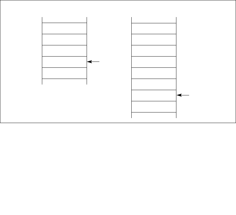
Vol. 3A 4-25
PROTECTION
4. Temporarily saves the current values of the SS and ESP registers.
5. Loads the segment selector and stack pointer for the new stack in the SS and ESP registers.
6. Pushes the temporarily saved values for the SS and ESP registers (for the calling
procedure) onto the new stack (see Figure 4-13).
7. Copies the number of parameter specified in the parameter count field of the call gate from
the calling procedure’s stack to the new stack. If the count is 0, no parameters are copied.
8. Pushes the return instruction pointer (the current contents of the CS and EIP registers) onto
the new stack.
9. Loads the segment selector for the new code segment and the new instruction pointer from
the call gate into the CS and EIP registers, respectively, and begins execution of the called
procedure.
See the description of the CALL instruction in Chapter 3, Instruction Set Reference, in the IA-32
Intel Architecture Software Developer’s Manual, Volume 2, for a detailed description of the priv-
ilege level checks and other protection checks that the processor performs on a far call through
a call gate.
The parameter count field in a call gate specifies the number of data items (up to 31) that the
processor should copy from the calling procedure’s stack to the stack of the called procedure. If
more than 31 data items need to be passed to the called procedure, one of the parameters can be
a pointer to a data structure, or the saved contents of the SS and ESP registers may be used to
access parameters in the old stack space. The size of the data items passed to the called proce-
dure depends on the call gate size, as described in Section 4.8.3, “Call Gates.”
Figure 4-13. Stack Switching During an Interprivilege-Level Call
Parameter 1
Parameter 2
Parameter 3
Calling SS
Calling ESP
Parameter 1
Parameter 2
Parameter 3
Calling CS
Calling EIP
Called Procedure’s Stack
ESP
ESP
Calling Procedure’s Stack

4-26 Vol. 3A
PROTECTION
4.8.5.1 Stack Switching in 64-bit Mode
Although protection-check rules for call gates are unchanged from 32-bit mode, stack-switch
changes in 64-bit mode are different.
When stacks are switched as part of a 64-bit mode privilege-level change through a call gate, a
new SS (stack segment) descriptor is not loaded; 64-bit mode only loads an inner-level RSP
from the TSS. The new SS is forced to NULL and the SS selector’s RPL field is forced to the
new CPL. The new SS is set to NULL in order to handle nested far transfers (CALLF, INTn,
interrupts and exceptions). The old SS and RSP are saved on the new stack.
On a subsequent RETF, the old SS is popped from the stack and loaded into the SS register. See
Table 4-2.
In 64-bit mode, stack operations resulting from a privilege-level-changing far call or far return
are eight-bytes wide and change the RSP by eight. The mode does not support the automatic
parameter-copy feature found in 32-bit mode. The call-gate count field is ignored. Software can
access the old stack, if necessary, by referencing the old stack-segment selector and stack pointer
saved on the new process stack.
In 64-bit mode, RETF is allowed to load a NULL SS under certain conditions. If the target mode
is 64-bit mode and the target CPL< >3, IRET allows SS to be loaded with a NULL selector. If
the called procedure itself is interrupted, the NULL SS is pushed on the stack frame. On the
subsequent RETF, the NULL SS on the stack acts as a flag to tell the processor not to load a new
SS descriptor.
4.8.6 Returning from a Called Procedure
The RET instruction can be used to perform a near return, a far return at the same privilege level,
and a far return to a different privilege level. This instruction is intended to execute returns from
procedures that were called with a CALL instruction. It does not support returns from a JMP
instruction, because the JMP instruction does not save a return instruction pointer on the stack.
A near return only transfers program control within the current code segment; therefore, the
processor performs only a limit check. When the processor pops the return instruction pointer
Table 4-2. 64-Bit-Mode Stack Layout After CALLF with CPL Change
32-bit Mode IA-32e mode
Old SS Selector +12 +24 Old SS Selector
Old ESP +8 +16 Old RSP
CS Selector +4 +8 Old CS Selector
EIP 0ESP RSP 0RIP
< 4 Bytes > < 8 Bytes >

Vol. 3A 4-27
PROTECTION
from the stack into the EIP register, it checks that the pointer does not exceed the limit of the
current code segment.
On a far return at the same privilege level, the processor pops both a segment selector for the
code segment being returned to and a return instruction pointer from the stack. Under normal
conditions, these pointers should be valid, because they were pushed on the stack by the CALL
instruction. However, the processor performs privilege checks to detect situations where the
current procedure might have altered the pointer or failed to maintain the stack properly.
A far return that requires a privilege-level change is only allowed when returning to a less priv-
ileged level (that is, the DPL of the return code segment is numerically greater than the CPL).
The processor uses the RPL field from the CS register value saved for the calling procedure (see
Figure 4-13) to determine if a return to a numerically higher privilege level is required. If the
RPL is numerically greater (less privileged) than the CPL, a return across privilege levels
occurs.
The processor performs the following steps when performing a far return to a calling procedure
(see Figures 6-2 and 6-4 in the IA-32 Intel® Architecture Software Developer’s Manual,
Volume 1, for an illustration of the stack contents prior to and after a return):
1. Checks the RPL field of the saved CS register value to determine if a privilege level
change is required on the return.
2. Loads the CS and EIP registers with the values on the called procedure’s stack. (Type and
privilege level checks are performed on the code-segment descriptor and RPL of the code-
segment selector.)
3. (If the RET instruction includes a parameter count operand and the return requires a
privilege level change.) Adds the parameter count (in bytes obtained from the RET
instruction) to the current ESP register value (after popping the CS and EIP values), to step
past the parameters on the called procedure’s stack. The resulting value in the ESP register
points to the saved SS and ESP values for the calling procedure’s stack. (Note that the byte
count in the RET instruction must be chosen to match the parameter count in the call gate
that the calling procedure referenced when it made the original call multiplied by the size
of the parameters.)
4. (If the return requires a privilege level change.) Loads the SS and ESP registers with the
saved SS and ESP values and switches back to the calling procedure’s stack. The SS and
ESP values for the called procedure’s stack are discarded. Any limit violations detected
while loading the stack-segment selector or stack pointer cause a general-protection
exception (#GP) to be generated. The new stack-segment descriptor is also checked for
type and privilege violations.
5. (If the RET instruction includes a parameter count operand.) Adds the parameter count (in
bytes obtained from the RET instruction) to the current ESP register value, to step past the
parameters on the calling procedure’s stack. The resulting ESP value is not checked against
the limit of the stack segment. If the ESP value is beyond the limit, that fact is not
recognized until the next stack operation.
6. (If the return requires a privilege level change.) Checks the contents of the DS, ES, FS, and
GS segment registers. If any of these registers refer to segments whose DPL is less than the

4-28 Vol. 3A
PROTECTION
new CPL (excluding conforming code segments), the segment register is loaded with a null
segment selector.
See the description of the RET instruction in Chapter 3, Instruction Set Reference, of the IA-32
Intel Architecture Software Developer’s Manual, Volume 2, for a detailed description of the priv-
ilege level checks and other protection checks that the processor performs on a far return.
4.8.7 Performing Fast Calls to System Procedures with the
SYSENTER and SYSEXIT Instructions
The SYSENTER and SYSEXIT instructions were introduced into the IA-32 architecture in the
Pentium II processors for the purpose of providing a fast (low overhead) mechanism for calling
operating system or executive procedures. SYSENTER is intended for use by user code running
at privilege level 3 to access operating system or executive procedures running at privilege level
0. SYSEXIT is intended for use by privilege level 0 operating system or executive procedures
for fast returns to privilege level 3 user code. SYSENTER can be executed from privilege levels
3, 2, 1, or 0; SYSEXIT can only be executed from privilege level 0.
The SYSENTER and SYSEXIT instructions are companion instructions, but they do not consti-
tute a call/return pair. This is because SYSENTER does not save any state information for use
by SYSEXIT on a return.
The target instruction and stack pointer for these instructions are not specified through instruc-
tion operands. Instead, they are specified through parameters entered in MSRs and general-
purpose registers.
For SYSENTER, target fields are generated using the following sources:
•Target code segment — Reads this from IA32_SYSENTER_CS.
•Target instruction — Reads this from IA32_SYSENTER_EIP.
•Stack segment — Computed by adding 8 to the value in IA32_SYSENTER_CS.
•Stack pointer — Reads this from the IA32_SYSENTER_ESP.
For SYSEXIT, target fields are generated using the following sources:
•Target code segment — Computed by adding 16 to the value in the
IA32_SYSENTER_CS.
•Target instruction — Reads this from EDX.
•Stack segment — Computed by adding 24 to the value in IA32_SYSENTER_CS.
•Stack pointer — Reads this from ECX.
The SYSENTER and SYSEXIT instructions preform “fast” calls and returns because they force
the processor into a predefined privilege level 0 state when SYSENTER is executed and into a
predefined privilege level 3 state when SYSEXIT is executed. By forcing predefined and consis-
tent processor states, the number of privilege checks ordinarily required to perform a far call to
another privilege levels are greatly reduced. Also, by predefining the target context state in

Vol. 3A 4-29
PROTECTION
MSRs and general-purpose registers eliminates all memory accesses except when fetching the
target code.
Any additional state that needs to be saved to allow a return to the calling procedure must be
saved explicitly by the calling procedure or be predefined through programming conventions.
4.8.7.1 SYSENTER and SYSEXIT Instructions in IA-32e Mode
For processors supporting Intel EM64T, the SYSENTER and SYSEXIT instructions are
enhanced to allow fast system calls from user code running at privilege level 3 (in compatibility
mode or 64-bit mode) to 64-bit executive procedures running at privilege level 0.
IA32_SYSENTER_EIP MSR and IA32_SYSENTER_ESP MSR are expanded to hold 64-bit
addresses. If IA-32e mode is inactive, only the lower 32-bit addresses stored in these MSRs are
used. If 64-bit mode is active, addresses stored in IA32_SYSENTER_EIP and
IA32_SYSENTER_ESP must be canonical. Note that, in 64-bit mode, IA32_SYSENTER_CS
must not contain a NULL selector.
When SYSENTER transfers control, the following fields are generated and bits set:
•Target code segment — Reads non-NULL selector from IA32_SYSENTER_CS.
•New CS attributes — CS base = 0, CS limit = FFFFFFFFH.
•Target instruction — Reads 64-bit canonical address from IA32_SYSENTER_EIP.
•Stack segment — Computed by adding 8 to the value from IA32_SYSENTER_CS.
•Stack pointer — Reads 64-bit canonical address from IA32_SYSENTER_ESP.
•New SS attributes — SS base = 0, SS limit = FFFFFFFFH.
When the SYSEXIT instruction transfers control to 64-bit mode user code using REX.W, the
following fields are generated and bits set:
•Target code segment — Computed by adding 32 to the value in IA32_SYSENTER_CS.
•New CS attributes — L-bit = 1 (go to 64-bit mode).
•Target instruction — Reads 64-bit canonical address in RDX.
•Stack segment — Computed by adding 40 to the value of IA32_SYSENTER_CS.
•Stack pointer — Update RSP using 64-bit canonical address in RCX.

4-30 Vol. 3A
PROTECTION
When SYSEXIT transfers control to compatibility mode user code when the operand size
attribute is 32 bits, the following fields are generated and bits set:
•Target code segment — Computed by adding 16 to the value in IA32_SYSENTER_CS.
•New CS attributes — L-bit = 0 (go to compatibility mode).
•Target instruction — Fetch the target instruction from 32-bit address in EDX.
•Stack segment — Computed by adding 24 to the value in IA32_SYSENTER_CS.
•Stack pointer — Update ESP from 32-bit address in ECX.
4.8.8 Fast System Calls in 64-bit Mode
The SYSCALL and SYSRET instructions are designed for operating systems that use a flat
memory model (segmentation is not used). The instructions, along with SYSENTER and
SYSEXIT, are suited for IA-32e mode operation. SYSCALL and SYSRET, however, are not
supported in compatibility mode. Use CPUID to check if SYSCALL and SYSRET are available
(CPUID.80000001H.EDX[bit 11] = 1).
SYSCALL is intended for use by user code running at privilege level 3 to access operating
system or executive procedures running at privilege level 0. SYSRET is intended for use by
privilege level 0 operating system or executive procedures for fast returns to privilege level 3
user code.
Stack pointers for SYSCALL/SYSRET are not specified through model specific registers. The
clearing of bits in RFLAGS is programmable rather than fixed. SYSCALL/SYSRET save and
restore the RFLAGS register.
For SYSCALL, the processor saves the RIP of the instruction in RCX and gets the privilege
level 0 target instruction and stack pointer from:
•Target code segment — Reads a non-NULL selector from IA32_STAR[47:32].
•Target instruction — Reads a 64-bit canonical address from IA32_LSTAR.
•Stack segment — Computed by adding 8 to the value in IA32_STAR[47:32].
•System flags — The processor uses a mask derived from IA32_FMASK to perform a
logical-AND operation with the lower 32-bits of RFLAGS. The result is saved into R11.
The mask is the complement of the value supplied by privileged executives using the
IA32_FMASK MSR.

Vol. 3A 4-31
PROTECTION
When SYSRET transfers control to 64-bit mode user code using REX.W, the processor gets the
privilege level 3 target instruction and stack pointer from:
•Target code segment — Reads a non-NULL selector from IA32_STAR[63:48] + 16.
•Target instruction — Copies the value in RCX into RIP.
•Stack segment — IA32_STAR[63:48] + 8.
•EFLAGS — Loaded from R11.
When SYSRET transfers control to 32-bit mode user code using a 32-bit operand size, the
processor gets the privilege level 3 target instruction and stack pointer from:
•Target code segment — Reads a non-NULL selector from IA32_STAR[63:48].
•Target instruction — Copies the value in ECX into EIP.
•Stack segment — IA32_STAR[63:48] + 8.
•EFLAGS — Loaded from R11.
It is the responsibility of the OS to ensure the descriptors in the GDT/LDT correspond to the
selectors loaded by SYSCALL/SYSRET (consistent with the base, limit, and attribute values
forced by the instructions).
Any address written to IA32_LSTAR is first checked by WRMSR to ensure canonical form. If
an address is not canonical, an exception is generated (#GP).
See Figure 4-14 for the layout of IA32_STAR, IA32_LSTAR and IA32_FMASK.
Figure 4-14. MSRs Used by SYSCALL and SYSRET
63 32 31 0
63 0
63 0
Target RIP for 64-bit Mode Calling Program
SYSRET CS and SS SYSCALL CS and SS
48 47
IA32_STAR
IA32_LSTAR
IA32_FMASK
32 31
SYSCALL EFLAGS Mask
Reserved
Reserved

4-32 Vol. 3A
PROTECTION
4.9 PRIVILEGED INSTRUCTIONS
Some of the system instructions (called “privileged instructions”) are protected from use by
application programs. The privileged instructions control system functions (such as the loading
of system registers). They can be executed only when the CPL is 0 (most privileged). If one of
these instructions is executed when the CPL is not 0, a general-protection exception (#GP) is
generated. The following system instructions are privileged instructions:
•LGDT — Load GDT register.
•LLDT — Load LDT register.
•LTR — Load task register.
•LIDT — Load IDT register.
•MOV (control registers) — Load and store control registers.
•LMSW — Load machine status word.
•CLTS — Clear task-switched flag in register CR0.
•MOV (debug registers) — Load and store debug registers.
•INVD — Invalidate cache, without writeback.
•WBINVD — Invalidate cache, with writeback.
•INVLPG —Invalidate TLB entry.
•HLT— Halt processor.
•RDMSR — Read Model-Specific Registers.
•WRMSR —Write Model-Specific Registers.
•RDPMC — Read Performance-Monitoring Counter.
•RDTSC — Read Time-Stamp Counter.
Some of the privileged instructions are available only in the more recent families of IA-32
processors (see Section 17.12., “New Instructions In the Pentium and Later IA-32 Processors”).
The PCE and TSD flags in register CR4 (bits 4 and 2, respectively) enable the RDPMC and
RDTSC instructions, respectively, to be executed at any CPL.
4.10 POINTER VALIDATION
When operating in protected mode, the processor validates all pointers to enforce protection
between segments and maintain isolation between privilege levels. Pointer validation consists
of the following checks:
1. Checking access rights to determine if the segment type is compatible with its use.
2. Checking read/write rights.

Vol. 3A 4-33
PROTECTION
3. Checking if the pointer offset exceeds the segment limit.
4. Checking if the supplier of the pointer is allowed to access the segment.
5. Checking the offset alignment.
The processor automatically performs first, second, and third checks during instruction execu-
tion. Software must explicitly request the fourth check by issuing an ARPL instruction. The fifth
check (offset alignment) is performed automatically at privilege level 3 if alignment checking is
turned on. Offset alignment does not affect isolation of privilege levels.
4.10.1 Checking Access Rights (LAR Instruction)
When the processor accesses a segment using a far pointer, it performs an access rights check
on the segment descriptor pointed to by the far pointer. This check is performed to determine if
type and privilege level (DPL) of the segment descriptor are compatible with the operation to be
performed. For example, when making a far call in protected mode, the segment-descriptor type
must be for a conforming or nonconforming code segment, a call gate, a task gate, or a TSS.
Then, if the call is to a nonconforming code segment, the DPL of the code segment must be equal
to the CPL, and the RPL of the code segment’s segment selector must be less than or equal to
the DPL. If type or privilege level are found to be incompatible, the appropriate exception is
generated.
To prevent type incompatibility exceptions from being generated, software can check the access
rights of a segment descriptor using the LAR (load access rights) instruction. The LAR instruc-
tion specifies the segment selector for the segment descriptor whose access rights are to be
checked and a destination register. The instruction then performs the following operations:
1. Check that the segment selector is not null.
2. Checks that the segment selector points to a segment descriptor that is within the descriptor
table limit (GDT or LDT).
3. Checks that the segment descriptor is a code, data, LDT, call gate, task gate, or TSS
segment-descriptor type.
4. If the segment is not a conforming code segment, checks if the segment descriptor is
visible at the CPL (that is, if the CPL and the RPL of the segment selector are less than or
equal to the DPL).
5. If the privilege level and type checks pass, loads the second doubleword of the segment
descriptor into the destination register (masked by the value 00FXFF00H, where X
indicates that the corresponding 4 bits are undefined) and sets the ZF flag in the EFLAGS
register. If the segment selector is not visible at the current privilege level or is an invalid
type for the LAR instruction, the instruction does not modify the destination register and
clears the ZF flag.
Once loaded in the destination register, software can preform additional checks on the access
rights information.

4-34 Vol. 3A
PROTECTION
4.10.2 Checking Read/Write Rights (VERR and VERW
Instructions)
When the processor accesses any code or data segment it checks the read/write privileges
assigned to the segment to verify that the intended read or write operation is allowed. Software
can check read/write rights using the VERR (verify for reading) and VERW (verify for writing)
instructions. Both these instructions specify the segment selector for the segment being checked.
The instructions then perform the following operations:
1. Check that the segment selector is not null.
2. Checks that the segment selector points to a segment descriptor that is within the descriptor
table limit (GDT or LDT).
3. Checks that the segment descriptor is a code or data-segment descriptor type.
4. If the segment is not a conforming code segment, checks if the segment descriptor is
visible at the CPL (that is, if the CPL and the RPL of the segment selector are less than or
equal to the DPL).
5. Checks that the segment is readable (for the VERR instruction) or writable (for the
VERW) instruction.
The VERR instruction sets the ZF flag in the EFLAGS register if the segment is visible at the
CPL and readable; the VERW sets the ZF flag if the segment is visible and writable. (Code
segments are never writable.) The ZF flag is cleared if any of these checks fail.
4.10.3 Checking That the Pointer Offset Is Within Limits (LSL
Instruction)
When the processor accesses any segment it performs a limit check to insure that the offset is
within the limit of the segment. Software can perform this limit check using the LSL (load
segment limit) instruction. Like the LAR instruction, the LSL instruction specifies the segment
selector for the segment descriptor whose limit is to be checked and a destination register. The
instruction then performs the following operations:
1. Check that the segment selector is not null.
2. Checks that the segment selector points to a segment descriptor that is within the descriptor
table limit (GDT or LDT).
3. Checks that the segment descriptor is a code, data, LDT, or TSS segment-descriptor type.
4. If the segment is not a conforming code segment, checks if the segment descriptor is
visible at the CPL (that is, if the CPL and the RPL of the segment selector less than or
equal to the DPL).

Vol. 3A 4-35
PROTECTION
5. If the privilege level and type checks pass, loads the unscrambled limit (the limit scaled
according to the setting of the G flag in the segment descriptor) into the destination register
and sets the ZF flag in the EFLAGS register. If the segment selector is not visible at the
current privilege level or is an invalid type for the LSL instruction, the instruction does not
modify the destination register and clears the ZF flag.
Once loaded in the destination register, software can compare the segment limit with the offset
of a pointer.
4.10.4 Checking Caller Access Privileges (ARPL Instruction)
The requestor’s privilege level (RPL) field of a segment selector is intended to carry the privi-
lege level of a calling procedure (the calling procedure’s CPL) to a called procedure. The called
procedure then uses the RPL to determine if access to a segment is allowed. The RPL is said to
“weaken” the privilege level of the called procedure to that of the RPL.
Operating-system procedures typically use the RPL to prevent less privileged application
programs from accessing data located in more privileged segments. When an operating-system
procedure (the called procedure) receives a segment selector from an application program (the
calling procedure), it sets the segment selector’s RPL to the privilege level of the calling proce-
dure. Then, when the operating system uses the segment selector to access its associated
segment, the processor performs privilege checks using the calling procedure’s privilege level
(stored in the RPL) rather than the numerically lower privilege level (the CPL) of the operating-
system procedure. The RPL thus insures that the operating system does not access a segment on
behalf of an application program unless that program itself has access to the segment.
Figure 4-15 shows an example of how the processor uses the RPL field. In this example, an
application program (located in code segment A) possesses a segment selector (segment selector
D1) that points to a privileged data structure (that is, a data structure located in a data segment
D at privilege level 0).
The application program cannot access data segment D, because it does not have sufficient priv-
ilege, but the operating system (located in code segment C) can. So, in an attempt to access data
segment D, the application program executes a call to the operating system and passes segment
selector D1 to the operating system as a parameter on the stack. Before passing the segment
selector, the (well behaved) application program sets the RPL of the segment selector to its
current privilege level (which in this example is 3). If the operating system attempts to access
data segment D using segment selector D1, the processor compares the CPL (which is now 0
following the call), the RPL of segment selector D1, and the DPL of data segment D (which is
0). Since the RPL is greater than the DPL, access to data segment D is denied. The processor’s
protection mechanism thus protects data segment D from access by the operating system,
because application program’s privilege level (represented by the RPL of segment selector B) is
greater than the DPL of data segment D.
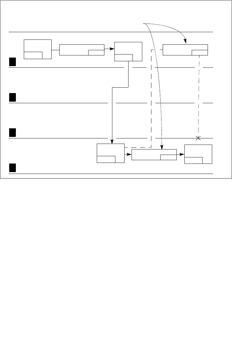
4-36 Vol. 3A
PROTECTION
Now assume that instead of setting the RPL of the segment selector to 3, the application program
sets the RPL to 0 (segment selector D2). The operating system can now access data segment D,
because its CPL and the RPL of segment selector D2 are both equal to the DPL of data segment D.
Because the application program is able to change the RPL of a segment selector to any value,
it can potentially use a procedure operating at a numerically lower privilege level to access a
protected data structure. This ability to lower the RPL of a segment selector breaches the
processor’s protection mechanism.
Because a called procedure cannot rely on the calling procedure to set the RPL correctly, oper-
ating-system procedures (executing at numerically lower privilege-levels) that receive segment
selectors from numerically higher privilege-level procedures need to test the RPL of the segment
selector to determine if it is at the appropriate level. The ARPL (adjust requested privilege level)
instruction is provided for this purpose. This instruction adjusts the RPL of one segment selector
to match that of another segment selector.
The example in Figure 4-15 demonstrates how the ARPL instruction is intended to be used.
When the operating-system receives segment selector D2 from the application program, it uses
the ARPL instruction to compare the RPL of the segment selector with the privilege level of the
Figure 4-15. Use of RPL to Weaken Privilege Level of Called Procedure
Passed as a
parameter on
the stack.
Access
allowed
Access
allowed
Application Program
Operating
System
Lowest Privilege
Highest Privilege
3
2
1
0
Data
Segment D
not
Segment Sel. D1
RPL=3
Segment Sel. D2
RPL=0
Gate Selector B
RPL=3
Code
Segment A
CPL=3
Code
Segment C
DPL=0
Call
Gate B
DPL=3
DPL=0

Vol. 3A 4-37
PROTECTION
application program (represented by the code-segment selector pushed onto the stack). If the
RPL is less than application program’s privilege level, the ARPL instruction changes the RPL
of the segment selector to match the privilege level of the application program (segment
selector D1). Using this instruction thus prevents a procedure running at a numerically higher
privilege level from accessing numerically lower privilege-level (more privileged) segments by
lowering the RPL of a segment selector.
Note that the privilege level of the application program can be determined by reading the RPL
field of the segment selector for the application-program’s code segment. This segment selector
is stored on the stack as part of the call to the operating system. The operating system can copy
the segment selector from the stack into a register for use as an operand for the ARPL
instruction.
4.10.5 Checking Alignment
When the CPL is 3, alignment of memory references can be checked by setting the AM flag in
the CR0 register and the AC flag in the EFLAGS register. Unaligned memory references
generate alignment exceptions (#AC). The processor does not generate alignment exceptions
when operating at privilege level 0, 1, or 2. See Table 5-7 for a description of the alignment
requirements when alignment checking is enabled.
4.11 PAGE-LEVEL PROTECTION
Page-level protection can be used alone or applied to segments. When page-level protection is
used with the flat memory model, it allows supervisor code and data (the operating system or
executive) to be protected from user code and data (application programs). It also allows pages
containing code to be write protected. When the segment- and page-level protection are
combined, page-level read/write protection allows more protection granularity within segments.
With page-level protection (as with segment-level protection) each memory reference is
checked to verify that protection checks are satisfied. All checks are made before the memory
cycle is started, and any violation prevents the cycle from starting and results in a page-fault
exception being generated. Because checks are performed in parallel with address translation,
there is no performance penalty.
The processor performs two page-level protection checks:
•Restriction of addressable domain (supervisor and user modes).
•Page type (read only or read/write).
Violations of either of these checks results in a page-fault exception being generated. See
Chapter 5, “Interrupt 14—Page-Fault Exception (#PF),” for an explanation of the page-fault
exception mechanism. This chapter describes the protection violations which lead to page-
fault exceptions.

4-38 Vol. 3A
PROTECTION
4.11.1 Page-Protection Flags
Protection information for pages is contained in two flags in a page-directory or page-table entry
(see Figure 3-14): the read/write flag (bit 1) and the user/supervisor flag (bit 2). The protection
checks are applied to both first- and second-level page tables (that is, page directories and page
tables).
4.11.2 Restricting Addressable Domain
The page-level protection mechanism allows restricting access to pages based on two privilege
levels:
•Supervisor mode (U/S flag is 0)—(Most privileged) For the operating system or executive,
other system software (such as device drivers), and protected system data (such as page
tables).
•User mode (U/S flag is 1)—(Least privileged) For application code and data.
The segment privilege levels map to the page privilege levels as follows. If the processor is
currently operating at a CPL of 0, 1, or 2, it is in supervisor mode; if it is operating at a CPL of
3, it is in user mode. When the processor is in supervisor mode, it can access all pages; when in
user mode, it can access only user-level pages. (Note that the WP flag in control register CR0
modifies the supervisor permissions, as described in Section 4.11.3, “Page Type.”)
Note that to use the page-level protection mechanism, code and data segments must be set up for
at least two segment-based privilege levels: level 0 for supervisor code and data segments and
level 3 for user code and data segments. (In this model, the stacks are placed in the data
segments.) To minimize the use of segments, a flat memory model can be used (see Section 3.2.1,
“Basic Flat Model”).
Here, the user and supervisor code and data segments all begin at address zero in the linear
address space and overlay each other. With this arrangement, operating-system code (running at
the supervisor level) and application code (running at the user level) can execute as if there are
no segments. Protection between operating-system and application code and data is provided by
the processor’s page-level protection mechanism.
4.11.3 Page Type
The page-level protection mechanism recognizes two page types:
•Read-only access (R/W flag is 0).
•Read/write access (R/W flag is 1).
When the processor is in supervisor mode and the WP flag in register CR0 is clear (its state
following reset initialization), all pages are both readable and writable (write-protection is
ignored). When the processor is in user mode, it can write only to user-mode pages that are

Vol. 3A 4-39
PROTECTION
read/write accessible. User-mode pages which are read/write or read-only are readable; super-
visor-mode pages are neither readable nor writable from user mode. A page-fault exception is
generated on any attempt to violate the protection rules.
The P6 family, Pentium, and Intel486 processors allow user-mode pages to be write-protected
against supervisor-mode access. Setting the WP flag in register CR0 to 1 enables supervisor-
mode sensitivity to user-mode, write protected pages. Supervisor pages which are read-only are
not writable from any privilege level, regardless of WP setting. This supervisor write-protect
feature is useful for implementing a “copy-on-write” strategy used by some operating systems,
such as UNIX*, for task creation (also called forking or spawning). When a new task is created,
it is possible to copy the entire address space of the parent task. This gives the child task a
complete, duplicate set of the parent's segments and pages. An alternative copy-on-write
strategy saves memory space and time by mapping the child's segments and pages to the same
segments and pages used by the parent task. A private copy of a page gets created only when
one of the tasks writes to the page. By using the WP flag and marking the shared pages as read-
only, the supervisor can detect an attempt to write to a user-level page, and can copy the page at
that time.
4.11.4 Combining Protection of Both Levels of Page Tables
For any one page, the protection attributes of its page-directory entry (first-level page table) may
differ from those of its page-table entry (second-level page table). The processor checks the
protection for a page in both its page-directory and the page-table entries. Table 4-3 shows the
protection provided by the possible combinations of protection attributes when the WP flag is
clear.
4.11.5 Overrides to Page Protection
The following types of memory accesses are checked as if they are privilege-level 0 accesses,
regardless of the CPL at which the processor is currently operating:
•Access to segment descriptors in the GDT, LDT, or IDT.
•Access to an inner-privilege-level stack during an inter-privilege-level call or a call to in
exception or interrupt handler, when a change of privilege level occurs.
4.12 COMBINING PAGE AND SEGMENT PROTECTION
When paging is enabled, the processor evaluates segment protection first, then evaluates page
protection. If the processor detects a protection violation at either the segment level or the page
level, the memory access is not carried out and an exception is generated. If an exception is
generated by segmentation, no paging exception is generated.
Page-level protections cannot be used to override segment-level protection. For example, a code
segment is by definition not writable. If a code segment is paged, setting the R/W flag for the
pages to read-write does not make the pages writable. Attempts to write into the pages will be
blocked by segment-level protection checks.

4-40 Vol. 3A
PROTECTION
Page-level protection can be used to enhance segment-level protection. For example, if a large
read-write data segment is paged, the page-protection mechanism can be used to write-protect
individual pages.
NOTE:
* If CR0.WP = 1, access type is determined by the R/W flags of the page-directory and page-table entries.
IF CR0.WP = 0, supervisor privilege permits read-write access.
4.13 PAGE-LEVEL PROTECTION AND EXECUTE-DISABLE BIT
In addition to page-level protection offered by the U/S and R/W flags, enhanced PAE-enabled
paging structures (see Section 3.10.3, “Enhanced Paging Data Structures”) provide the execute-
disable bit. This bit offers additional protection for data pages.
An IA-32 processor with the execute disable bit capability can prevent data pages from being
used by malicious software to execute code. This capability is provided in:
•32-bit protected mode with PAE enabled.
•IA-32e mode.
Table 4-3. Combined Page-Directory and Page-Table Protection
Page-Directory Entry Page-Table Entry Combined Effect
Privilege Access Type Privilege Access Type Privilege Access Type
User Read-Only User Read-Only User Read-Only
User Read-Only User Read-Write User Read-Only
User Read-Write User Read-Only User Read-Only
User Read-Write User Read-Write User Read/Write
User Read-Only Supervisor Read-Only Supervisor Read/Write*
User Read-Only Supervisor Read-Write Supervisor Read/Write*
User Read-Write Supervisor Read-Only Supervisor Read/Write*
User Read-Write Supervisor Read-Write Supervisor Read/Write
Supervisor Read-Only User Read-Only Supervisor Read/Write*
Supervisor Read-Only User Read-Write Supervisor Read/Write*
Supervisor Read-Write User Read-Only Supervisor Read/Write*
Supervisor Read-Write User Read-Write Supervisor Read/Write
Supervisor Read-Only Supervisor Read-Only Supervisor Read/Write*
Supervisor Read-Only Supervisor Read-Write Supervisor Read/Write*
Supervisor Read-Write Supervisor Read-Only Supervisor Read/Write*
Supervisor Read-Write Supervisor Read-Write Supervisor Read/Write

Vol. 3A 4-41
PROTECTION
While the execute disable bit capability does not introduce new instructions, it does require
operating systems to use a PAE-enabled environment and establish a page-granular protection
policy for memory pages.
If the execute disable bit of a memory page is set, that page can be used only as data. An
attempt to execute code from a memory page with the execute-disable bit set causes a page-
fault exception.
The page sizes and physical address sizes supported by execute disable bit capability are shown
in Table 4-4. Existing page-level protection mechanisms (see Section 4.11, “Page-Level Protec-
tion”) continue to apply to memory pages independent of the execute-disable bit setting.
4.13.1 Detecting and Enabling the Execute-Disable Bit Capability
Detect the presence of the execute disable bit capability using the CPUID instruction.
CPUID.80000001H. EDX[bit 20] = 1 indicates the bit is available.
If the bit is available and PAE is enabled, enable the execute disable bit capability by setting the
IA32_EFER.NXE[bit 11] = 1. IA32_EFER is available if CPUID.80000001H.EDX[bit 20 or
29] = 1.
If the execute disable bit capability is not available, a write to IA32_EFER.NXE produces a #GP
exception. See Table 4-5.
4.13.2 Execute-Disable Bit Page Protection
The execute-disable bit in paging structures enhances page protection for data pages. Memory
pages that contain data cannot be used to execute code if IA32_EFER.NXE =1 and the execute-
disable bit of the memory page is set. Table 4-6 lists the valid usage of a page in relation to the
value of execute-disable bit (bit 63) of the corresponding entry in each level of the paging struc-
Table 4-4. Page Sizes and Physical Address Sizes Supported by
Execute-Disable Bit Capability
PG Flag,
CR0 PAE Flag,
CR4 PS Flag,
PDE CPUID Feature
Flag ECX[IA-32e] Page Size Physical Address Size
1 1 0 0 4 KBytes Implementation specific
1 1 1 0 2 MBytes Implementation specific
1 1 0 1 4 KBytes 40 Bits
1 1 1 1 2 MBytes 40 Bits
Table 4-5. Extended Feature Enable MSR (IA32_EFER)
63:12 11 10 9 8 7:1 0
Reserved Execute-
disable bit
enable (NXE)
IA-32e mode
active (LMA) Reserved IA-32e mode
enable (LME) Reserved SysCall enable
(SCE)

4-42 Vol. 3A
PROTECTION
tures. Execute-disable bit protection can be activated using the execute-disable bit at any level
of the paging structure, irrespective of the corresponding entry in other levels. When execute-
disable-bit protection is not activated, the page can be used as code or data.
In legacy PAE-enabled mode, Table 4-7 and Table 4-8 show the effect of setting the execute-
disable bit for code and data pages.
Table 4-6. IA-32e Mode Page Level Protection Matrix
with Execute-Disable Bit Capability
Execute Disable Bit Value (Bit 63) Valid Usage
PML4 PDP PDE PTE
Bit 63 = 1 * * * Data
*Bit 63 = 1 * * Data
* * Bit 63 = 1 * Data
* * * Bit 63 = 1 Data
Bit 63 = 0 Bit 63 = 0 Bit 63 = 0 Bit 63 = 0 Data/Code
NOTE:
* Value not checked.
Table 4-7. Legacy PAE-Enabled 4-KByte Page Level Protection Matrix
with Execute-Disable Bit Capability
Execute Disable Bit Value (Bit 63) Valid Usage
PDE PTE
Bit 63 = 1 * Data
* Bit 63 = 1 Data
Bit 63 = 0 Bit 63 = 0 Data/Code
NOTE:
* Value not checked.
Table 4-8. Legacy PAE-Enabled 2-MByte Page Level Protection
with Execute-Disable Bit Capability
Execute Disable Bit Value (Bit 63) Valid Usage
PDE
Bit 63 = 1 Data
Bit 63 = 0 Data/Code

Vol. 3A 4-43
PROTECTION
4.13.3 Reserved Bit Checking
The processor enforces reserved bit checking in paging data structure entries. The bits being
checked varies with paging mode and may vary with the size of physical address space.
Table 4-9 shows the reserved bits that are checked when the execute disable bit capability is
enabled (CR4.PAE = 1 and IA32_EFER.NXE = 1). Table 4-9 and Table 4-10 show the
following paging modes:
•Non-PAE 4-KByte paging: 4-KByte-page only paging (CR4.PAE = 0, CR4.PSE = 0).
•PSE36: 4-KByte and 4-MByte pages (CR4.PAE = 0, CR4.PSE = 1).
•PAE: 4-KByte and 2-MByte pages (CR4.PAE = 1, CR4.PSE = X).
In legacy PAE-enabled paging, some processors may only support a 36-bit (or 32-bit) physical
address size; in such cases reserved bit checking still applies to bits 39:36 (or bits 39:32). See
the table note.
If execute disable bit capability is not enabled or not available, reserved bit checking in 64-bit
mode includes bit 63 and additional bits. This and reserved bit checking for legacy 32-bit paging
modes are shown in Table 4-10.
Table 4-9. IA-32e Mode Page Level Protection Matrix
with Execute-Disable Bit Capability Enabled
Mode Paging Mode Check Bits
32-bit 4-KByte paging (non-PAE) No reserved bits checked
PSE36 - PDE, 4-MByte page Bit [21]
PSE36 - PDE, 4-KByte page No reserved bits checked
PSE36 - PTE No reserved bits checked
PAE - PDP table entry Bits [63:40] & [8:5] & [2:1]1
PAE - PDE, 2-MByte page Bits [62:40] & [20:13]1
PAE - PDE, 4-KByte page Bits [62:40]1
PAE - PTE Bits [62:40]1
64-bit PML4E Bits [51:40]
PDPTE Bits [51:40]
PDE, 2-MByte page Bits [51:40] & [20:13]
PDE, 4-KByte page Bits [51:40]
PTE Bits [51:40]
NOTE:
1. Reserved bit checking also applies to bits 39:36 for processors that support only 36-bits of physical
address. For processor that support only 32 bits of physical address, reserved bit checking also applies
to bits 39:32.

4-44 Vol. 3A
PROTECTION
Table 4-10. Reserved Bit Checking WIth Execute-Disable Bit Capability Not Enabled
4.13.4 Exception Handling
When execute disable bit capability is enabled (IA32_EFER.NXE = 1), conditions for a page
fault to occur include the same conditions that apply to an IA-32 processor without execute
disable bit capability plus the following new condition: an instruction fetch to a linear address
that translates to physical address in a memory page that has the execute-disable bit set.
An Execute Disable Bit page fault can occur at all privilege levels. It can occur on any instruc-
tion fetch, including (but not limited to): near branches, far branches, CALL/RET/INT/IRET
execution, sequential instruction fetches, and task switches. The execute-disable bit in the page
translation mechanism is checked only when:
•IA32_EFER.NXE = 1.
•The instruction translation look-aside buffer (ITLB) is loaded with a page that is not
already present in the ITLB.
Mode Paging Mode Check Bits
32-bit KByte paging (non-PAE) No reserved bits checked
PSE36 - PDE, 4-MByte page Bit [21]
PSE36 - PDE, 4-KByte page No reserved bits checked
PSE36 - PTE No reserved bits checked
PAE - PDP table entry Bits [63:40] & [8:5] & [2:1]1
PAE - PDE, 2-MByte page Bits [63:40] & [20:13]1
PAE - PDE, 4-KByte page Bits [63:40]1
PAE - PTE Bits [63:40]1
64-bit PML4E Bit [63], bits [51:40]
PDPTE Bit [63], bits [51:40]
PDE, 2-MByte page Bit [63], bits [51:40] & [20:13]
PDE, 4-KByte page Bit [63], bits [51:40]
PTE Bit [63], bits [51:40]
NOTES:
1. Reserved bit checking also applies to bits 39:36 for processors that support only 36-bits of physical
address. For processor that support only 32 bits of physical address, reserved bit checking also applies
to bits 39:32.

5
Interrupt and
Exception Handling

Vol. 3A 5-1
CHAPTER 5
INTERRUPT AND EXCEPTION HANDLING
This chapter describes the processor’s interrupt and exception-handling mechanism when oper-
ating in protected mode. Most of the information provided here also applies to interrupt and
exception mechanisms used in real-address, virtual-8086 mode, and 64-bit mode.
Chapter 15, “8086 Emulation,” describes information specific to interrupt and exception mech-
anisms in real-address and virtual-8086 mode. Section 5.14, “Exception and Interrupt Handling
in 64-bit Mode,” describes information specific to interrupt and exception mechanisms in
IA-32e mode and 64-bit sub-mode.
5.1 INTERRUPT AND EXCEPTION OVERVIEW
Interrupts and exceptions are events that indicate that a condition exists somewhere in the
system, the processor, or within the currently executing program or task that requires the atten-
tion of a processor. They typically result in a forced transfer of execution from the currently
running program or task to a special software routine or task called an interrupt handler or an
exception handler. The action taken by a processor in response to an interrupt or exception is
referred to as servicing or handling the interrupt or exception.
Interrupts occur at random times during the execution of a program, in response to signals from
hardware. System hardware uses interrupts to handle events external to the processor, such as
requests to service peripheral devices. Software can also generate interrupts by executing the
INT n instruction.
Exceptions occur when the processor detects an error condition while executing an instruction,
such as division by zero. The processor detects a variety of error conditions including protection
violations, page faults, and internal machine faults. The machine-check architecture of the
Pentium 4, Intel Xeon, P6 family, and Pentium processors also permits a machine-check excep-
tion to be generated when internal hardware errors and bus errors are detected.
When an interrupt is received or an exception is detected, the currently running procedure or
task is suspended while the processor executes an interrupt or exception handler. When execu-
tion of the handler is complete, the processor resumes execution of the interrupted procedure or
task. The resumption of the interrupted procedure or task happens without loss of program conti-
nuity, unless recovery from an exception was not possible or an interrupt caused the currently
running program to be terminated.
This chapter describes the processor’s interrupt and exception-handling mechanism, when oper-
ating in protected mode. A description of the exceptions and the conditions that cause them to
be generated is given at the end of this chapter.

5-2 Vol. 3A
INTERRUPT AND EXCEPTION HANDLING
5.2 EXCEPTION AND INTERRUPT VECTORS
To aid in handling exceptions and interrupts, each IA-32 architecture-defined exception and
each interrupt condition that requires special handling by the processor is assigned a unique
identification number, called a vector. The processor uses the vector assigned to an exception or
interrupt as an index into the interrupt descriptor table (IDT). The table provides the entry point
to an exception or interrupt handler (see Section 5.10, “Interrupt Descriptor Table (IDT)”).
The allowable range for vector numbers is 0 to 255. Vectors in the range 0 through 31 are
reserved by the IA-32 architecture for architecture-defined exceptions and interrupts. Not all of
the vectors in this range have a currently defined function. The unassigned vectors in this range
are reserved. Do not use the reserved vectors.
The vectors in the range 32 to 255 are designated as user-defined interrupts and are not reserved
by the IA-32 architecture. These interrupts are generally assigned to external I/O devices to
enable those devices to send interrupts to the processor through one of the external hardware
interrupt mechanisms (see Section 5.3, “Sources of Interrupts”).
Table 5-1 shows vector assignments for architecturally defined exceptions and for the NMI
interrupt. This table gives the exception type (see Section 5.5, “Exception Classifications”) and
indicates whether an error code is saved on the stack for the exception. The source of each
predefined exception and the NMI interrupt is also given.
5.3 SOURCES OF INTERRUPTS
The processor receives interrupts from two sources:
•External (hardware generated) interrupts.
•Software-generated interrupts.
5.3.1 External Interrupts
External interrupts are received through pins on the processor or through the local APIC. The
primary interrupt pins on Pentium 4, Intel Xeon, P6 family, and Pentium processors are the
LINT[1:0] pins, which are connected to the local APIC (see Chapter 8, “Advanced Program-
mable Interrupt Controller (APIC)”). When the local APIC is enabled, the LINT[1:0] pins can
be programmed through the APIC’s local vector table (LVT) to be associated with any of the
processor’s exception or interrupt vectors.
When the local APIC is disabled, these pins are configured as INTR and NMI pins, respectively.
Asserting the INTR pin signals the processor that an external interrupt has occurred. The
processor reads from the system bus the interrupt vector number provided by an external inter-
rupt controller, such as an 8259A (see Section 5.2, “Exception and Interrupt Vectors”). Asserting
the NMI pin signals a non-maskable interrupt (NMI), which is assigned to interrupt vector 2.

Vol. 3A 5-3
INTERRUPT AND EXCEPTION HANDLING
Table 5-1. Protected-Mode Exceptions and Interrupts
Vector
No. Mne-
monic Description Type Error
Code Source
0 #DE Divide Error Fault No DIV and IDIV instructions.
1 #DB RESERVED Fault/
Trap No For Intel use only.
2 — NMI Interrupt Interrupt No Nonmaskable external interrupt.
3 #BP Breakpoint Trap No INT 3 instruction.
4 #OF Overflow Trap No INTO instruction.
5 #BR BOUND Range Exceeded Fault No BOUND instruction.
6 #UD Invalid Opcode (Undefined
Opcode) Fault No UD2 instruction or reserved
opcode.1
7 #NM Device Not Available (No
Math Coprocessor) Fault No Floating-point or WAIT/FWAIT
instruction.
8 #DF Double Fault Abort Yes
(zero) Any instruction that can generate
an exception, an NMI, or an
INTR.
9 Coprocessor Segment
Overrun (reserved) Fault No Floating-point instruction.2
10 #TS Invalid TSS Fault Yes Task switch or TSS access.
11 #NP Segment Not Present Fault Yes Loading segment registers or
accessing system segments.
12 #SS Stack-Segment Fault Fault Yes Stack operations and SS register
loads.
13 #GP General Protection Fault Yes Any memory reference and other
protection checks.
14 #PF Page Fault Fault Yes Any memory reference.
15 — (Intel reserved. Do not use.) No
16 #MF x87 FPU Floating-Point
Error (Math Fault) Fault No x87 FPU floating-point or
WAIT/FWAIT instruction.
17 #AC Alignment Check Fault Yes
(Zero) Any data reference in memory.3
18 #MC Machine Check Abort No Error codes (if any) and source
are model dependent.4
19 #XF SIMD Floating-Point
Exception Fault No SSE/SSE2/SSE3 floating-point
instructions5
20-31 — Intel reserved. Do not use.
32-255 — User Defined (Non-
reserved) Interrupts Interrupt External interrupt or INT n
instruction.
NOTES:
1. The UD2 instruction was introduced in the Pentium Pro processor.
2. IA-32 processors after the Intel386 processor do not generate this exception.
3. This exception was introduced in the Intel486 processor.
4. This exception was introduced in the Pentium processor and enhanced in the P6 family processors.
5. This exception was introduced in the Pentium III processor.

5-4 Vol. 3A
INTERRUPT AND EXCEPTION HANDLING
The processor’s local APIC is normally connected to a system-based I/O APIC. Here, external
interrupts received at the I/O APIC’s pins can be directed to the local APIC through the system
bus (Pentium 4 and Intel Xeon processors) or the APIC serial bus (P6 family and Pentium
processors). The I/O APIC determines the vector number of the interrupt and sends this number
to the local APIC. When a system contains multiple processors, processors can also send inter-
rupts to one another by means of the system bus (Pentium 4 and Intel Xeon processors) or the
APIC serial bus (P6 family and Pentium processors).
The LINT[1:0] pins are not available on the Intel486 processor and earlier Pentium processors
that do not contain an on-chip local APIC. These processors have dedicated NMI and INTR
pins. With these processors, external interrupts are typically generated by a system-based inter-
rupt controller (8259A), with the interrupts being signaled through the INTR pin.
Note that several other pins on the processor can cause a processor interrupt to occur. However,
these interrupts are not handled by the interrupt and exception mechanism described in this
chapter. These pins include the RESET#, FLUSH#, STPCLK#, SMI#, R/S#, and INIT# pins.
The pins are included on a particular IA-32 processor is implementation dependent. The func-
tions of these pins are described in the data books for the individual processors. The SMI# pin
is described in Chapter 24, “System Management.”
5.3.2 Maskable Hardware Interrupts
Any external interrupt that is delivered to the processor by means of the INTR pin or through
the local APIC is called a maskable hardware interrupt. Maskable hardware interrupts that can
be delivered through the INTR pin include all IA-32 architecture defined interrupt vectors from
0 through 255; those that can be delivered through the local APIC include interrupt vectors 16
through 255.
The IF flag in the EFLAGS register permits all maskable hardware interrupts to be masked as a
group (see Section 5.8.1, “Masking Maskable Hardware Interrupts”). Note that when interrupts
0 through 15 are delivered through the local APIC, the APIC indicates the receipt of an illegal
vector.
5.3.3 Software-Generated Interrupts
The INT n instruction permits interrupts to be generated from within software by supplying an
interrupt vector number as an operand. For example, the INT 35 instruction forces an implicit
call to the interrupt handler for interrupt 35.
Any of the interrupt vectors from 0 to 255 can be used as a parameter in this instruction. If the
processor’s predefined NMI vector is used, however, the response of the processor will not be
the same as it would be from an NMI interrupt generated in the normal manner. If vector number
2 (the NMI vector) is used in this instruction, the NMI interrupt handler is called, but the
processor’s NMI-handling hardware is not activated.
Interrupts generated in software with the INT n instruction cannot be masked by the IF flag in
the EFLAGS register.

Vol. 3A 5-5
INTERRUPT AND EXCEPTION HANDLING
5.4 SOURCES OF EXCEPTIONS
The processor receives exceptions from three sources:
•Processor-detected program-error exceptions.
•Software-generated exceptions.
•Machine-check exceptions.
5.4.1 Program-Error Exceptions
The processor generates one or more exceptions when it detects program errors during the
execution in an application program or the operating system or executive. The IA-32 architec-
ture defines a vector number for each processor-detectable exception. Exceptions are classified
as faults, traps, and aborts (see Section 5.5, “Exception Classifications”).
5.4.2 Software-Generated Exceptions
The INTO, INT 3, and BOUND instructions permit exceptions to be generated in software.
These instructions allow checks for exception conditions to be performed at points in the
instruction stream. For example, INT 3 causes a breakpoint exception to be generated.
The INT n instruction can be used to emulate exceptions in software; but there is a limitation. If
INT n provides a vector for one of the IA-32 architecture exceptions, the processor generates an
interrupt to the correct vector (to access the exception handler) but does not push an error code
on the stack. This is true even if the associated hardware-generated exception normally produces
an error code. The exception handler will still attempt to pop an error code from the stack while
handling the exception. Because no error code was pushed, the handler will pop off and discard
the EIP instead (in place of the missing error code). This sends the return to the wrong location.
5.4.3 Machine-Check Exceptions
The P6 family and Pentium processors provide both internal and external machine-check mech-
anisms for checking the operation of the internal chip hardware and bus transactions. These
implementation dependent. When a machine-check error is detected, the processor signals a
machine-check exception (vector 18) and returns an error code.
See Chapter 5, “Interrupt 18—Machine-Check Exception (#MC)” and Chapter 14, “Machine-
Check Architecture,” for more information about the machine-check mechanism.
5.5 EXCEPTION CLASSIFICATIONS
Exceptions are classified as faults, traps, or aborts depending on the way they are reported and
whether the instruction that caused the exception can be restarted without loss of program or task
continuity.

5-6 Vol. 3A
INTERRUPT AND EXCEPTION HANDLING
•Faults — A fault is an exception that can generally be corrected and that, once corrected,
allows the program to be restarted with no loss of continuity. When a fault is reported, the
processor restores the machine state to the state prior to the beginning of execution of the
faulting instruction. The return address (saved contents of the CS and EIP registers) for the
fault handler points to the faulting instruction, rather than to the instruction following the
faulting instruction.
•Traps — A trap is an exception that is reported immediately following the execution of the
trapping instruction. Traps allow execution of a program or task to be continued without
loss of program continuity. The return address for the trap handler points to the instruction
to be executed after the trapping instruction.
•Aborts — An abort is an exception that does not always report the precise location of the
instruction causing the exception and does not allow a restart of the program or task that
caused the exception. Aborts are used to report severe errors, such as hardware errors and
inconsistent or illegal values in system tables.
NOTE
One exception subset normally reported as a fault is not restartable. Such
exceptions result in loss of some processor state. For example, executing a
POPAD instruction where the stack frame crosses over the end of the stack
segment causes a fault to be reported. In this situation, the exception handler
sees that the instruction pointer (CS:EIP) has been restored as if the POPAD
instruction had not been executed. However, internal processor state (the
general-purpose registers) will have been modified. Such cases are
considered programming errors. An application causing this class of
exceptions should be terminated by the operating system.
5.6 PROGRAM OR TASK RESTART
To allow the restarting of program or task following the handling of an exception or an interrupt,
all exceptions (except aborts) are guaranteed to report exceptions on an instruction boundary.
All interrupts are guaranteed to be taken on an instruction boundary.
For fault-class exceptions, the return instruction pointer (saved when the processor generates an
exception) points to the faulting instruction. So, when a program or task is restarted following
the handling of a fault, the faulting instruction is restarted (re-executed). Restarting the faulting
instruction is commonly used to handle exceptions that are generated when access to an operand
is blocked. The most common example of this type of fault is a page-fault exception (#PF) that
occurs when a program or task references an operand located on a page that is not in memory.
When a page-fault exception occurs, the exception handler can load the page into memory and
resume execution of the program or task by restarting the faulting instruction. To insure that the
restart is handled transparently to the currently executing program or task, the processor saves
the necessary registers and stack pointers to allow a restart to the state prior to the execution of
the faulting instruction.

Vol. 3A 5-7
INTERRUPT AND EXCEPTION HANDLING
For trap-class exceptions, the return instruction pointer points to the instruction following the
trapping instruction. If a trap is detected during an instruction which transfers execution, the
return instruction pointer reflects the transfer. For example, if a trap is detected while executing
a JMP instruction, the return instruction pointer points to the destination of the JMP instruction,
not to the next address past the JMP instruction. All trap exceptions allow program or task restart
with no loss of continuity. For example, the overflow exception is a trap exception. Here, the
return instruction pointer points to the instruction following the INTO instruction that tested
EFLAGS.OF (overflow) flag. The trap handler for this exception resolves the overflow condi-
tion. Upon return from the trap handler, program or task execution continues at the instruction
following the INTO instruction.
The abort-class exceptions do not support reliable restarting of the program or task. Abort
handlers are designed to collect diagnostic information about the state of the processor when the
abort exception occurred and then shut down the application and system as gracefully as
possible.
Interrupts rigorously support restarting of interrupted programs and tasks without loss of conti-
nuity. The return instruction pointer saved for an interrupt points to the next instruction to be
executed at the instruction boundary where the processor took the interrupt. If the instruction
just executed has a repeat prefix, the interrupt is taken at the end of the current iteration with the
registers set to execute the next iteration.
The ability of a P6 family processor to speculatively execute instructions does not affect the
taking of interrupts by the processor. Interrupts are taken at instruction boundaries located
during the retirement phase of instruction execution; so they are always taken in the “in-order”
instruction stream. See Chapter 2, “IA-32 Intel® Architecture,” in the IA-32 Intel® Architecture
Software Developer’s Manual, Volume 1, for more information about the P6 family processors’
microarchitecture and its support for out-of-order instruction execution.
Note that the Pentium processor and earlier IA-32 processors also perform varying amounts of
prefetching and preliminary decoding. With these processors as well, exceptions and interrupts
are not signaled until actual “in-order” execution of the instructions. For a given code sample,
the signaling of exceptions occurs uniformly when the code is executed on any family of IA-32
processors (except where new exceptions or new opcodes have been defined).

5-8 Vol. 3A
INTERRUPT AND EXCEPTION HANDLING
5.7 NONMASKABLE INTERRUPT (NMI)
The nonmaskable interrupt (NMI) can be generated in either of two ways:
•External hardware asserts the NMI pin.
•The processor receives a message on the system bus (Pentium 4 and Intel Xeon processors)
or the APIC serial bus (P6 family and Pentium processors) with a delivery mode NMI.
When the processor receives a NMI from either of these sources, the processor handles it imme-
diately by calling the NMI handler pointed to by interrupt vector number 2. The processor also
invokes certain hardware conditions to insure that no other interrupts, including NMI interrupts,
are received until the NMI handler has completed executing (see Section 5.7.1, “Handling
Multiple NMIs”).
Also, when an NMI is received from either of the above sources, it cannot be masked by the IF
flag in the EFLAGS register.
It is possible to issue a maskable hardware interrupt (through the INTR pin) to vector 2 to invoke
the NMI interrupt handler; however, this interrupt will not truly be an NMI interrupt. A true NMI
interrupt that activates the processor’s NMI-handling hardware can only be delivered through
one of the mechanisms listed above.
5.7.1 Handling Multiple NMIs
While an NMI interrupt handler is executing, the processor disables additional calls to the NMI
handler until the next IRET instruction is executed. This blocking of subsequent NMIs prevents
stacking up calls to the NMI handler. It is recommended that the NMI interrupt handler be
accessed through an interrupt gate to disable maskable hardware interrupts (see Section 5.8.1,
“Masking Maskable Hardware Interrupts”). If the NMI handler is a virtual-8086 task with an
IOPL of less than 3, an IRET instruction issued from the handler generates a general-protection
exception (see Section 15.2.7, “Sensitive Instructions”). In this case, the NMI is unmasked
before the general-protection exception handler is invoked.
5.8 ENABLING AND DISABLING INTERRUPTS
The processor inhibits the generation of some interrupts, depending on the state of the processor
and of the IF and RF flags in the EFLAGS register, as described in the following sections.

Vol. 3A 5-9
INTERRUPT AND EXCEPTION HANDLING
5.8.1 Masking Maskable Hardware Interrupts
The IF flag can disable the servicing of maskable hardware interrupts received on the
processor’s INTR pin or through the local APIC (see Section 5.3.2, “Maskable Hardware Inter-
rupts”). When the IF flag is clear, the processor inhibits interrupts delivered to the INTR pin or
through the local APIC from generating an internal interrupt request; when the IF flag is set,
interrupts delivered to the INTR or through the local APIC pin are processed as normal external
interrupts.
The IF flag does not affect non-maskable interrupts (NMIs) delivered to the NMI pin or delivery
mode NMI messages delivered through the local APIC, nor does it affect processor generated
exceptions. As with the other flags in the EFLAGS register, the processor clears the IF flag in
response to a hardware reset.
The fact that the group of maskable hardware interrupts includes the reserved interrupt and
exception vectors 0 through 32 can potentially cause confusion. Architecturally, when the IF
flag is set, an interrupt for any of the vectors from 0 through 32 can be delivered to the processor
through the INTR pin and any of the vectors from 16 through 32 can be delivered through the
local APIC. The processor will then generate an interrupt and call the interrupt or exception
handler pointed to by the vector number. So for example, it is possible to invoke the page-fault
handler through the INTR pin (by means of vector 14); however, this is not a true page-fault
exception. It is an interrupt. As with the INT n instruction (see Section 5.4.2, “Software-Gener-
ated Exceptions”), when an interrupt is generated through the INTR pin to an exception vector,
the processor does not push an error code on the stack, so the exception handler may not operate
correctly.
The IF flag can be set or cleared with the STI (set interrupt-enable flag) and CLI (clear interrupt-
enable flag) instructions, respectively. These instructions may be executed only if the CPL is
equal to or less than the IOPL. A general-protection exception (#GP) is generated if they are
executed when the CPL is greater than the IOPL. (The effect of the IOPL on these instructions
is modified slightly when the virtual mode extension is enabled by setting the VME flag in
control register CR4: see Section 15.3, “Interrupt and Exception Handling in Virtual-8086
Mode.” Behavior is also impacted by the PVI flag: see Section 15.4, “Protected-Mode Virtual
Interrupts.”
The IF flag is also affected by the following operations:
•The PUSHF instruction stores all flags on the stack, where they can be examined and
modified. The POPF instruction can be used to load the modified flags back into the
EFLAGS register.
•Task switches and the POPF and IRET instructions load the EFLAGS register; therefore,
they can be used to modify the setting of the IF flag.
•When an interrupt is handled through an interrupt gate, the IF flag is automatically cleared,
which disables maskable hardware interrupts. (If an interrupt is handled through a trap
gate, the IF flag is not cleared.)
See the descriptions of the CLI, STI, PUSHF, POPF, and IRET instructions in Chapter 3,
“Instruction Set Reference, A-M,” in the IA-32 Intel® Architecture Software Developer’s

5-10 Vol. 3A
INTERRUPT AND EXCEPTION HANDLING
Manual, Volume 2A, for a detailed description of the operations these instructions are allowed
to perform on the IF flag.
5.8.2 Masking Instruction Breakpoints
The RF (resume) flag in the EFLAGS register controls the response of the processor to instruc-
tion-breakpoint conditions (see the description of the RF flag in Section 2.3, “System Flags and
Fields in the EFLAGS Register”).
When set, it prevents an instruction breakpoint from generating a debug exception (#DB); when
clear, instruction breakpoints will generate debug exceptions. The primary function of the RF
flag is to prevent the processor from going into a debug exception loop on an instruction-break-
point. See Section 18.3.1.1, “Instruction-Breakpoint Exception Condition,” for more informa-
tion on the use of this flag.
5.8.3 Masking Exceptions and Interrupts When Switching
Stacks
To switch to a different stack segment, software often uses a pair of instructions, for example:
MOV SS, AX
MOV ESP, StackTop
If an interrupt or exception occurs after the segment selector has been loaded into the SS register
but before the ESP register has been loaded, these two parts of the logical address into the stack
space are inconsistent for the duration of the interrupt or exception handler.
To prevent this situation, the processor inhibits interrupts, debug exceptions, and single-step trap
exceptions after either a MOV to SS instruction or a POP to SS instruction, until the instruction
boundary following the next instruction is reached. All other faults may still be generated. If the
LSS instruction is used to modify the contents of the SS register (which is the recommended
method of modifying this register), this problem does not occur.
5.9 PRIORITY AMONG SIMULTANEOUS EXCEPTIONS AND
INTERRUPTS
If more than one exception or interrupt is pending at an instruction boundary, the processor
services them in a predictable order. Table 5-2 shows the priority among classes of exception
and interrupt sources.

Vol. 3A 5-11
INTERRUPT AND EXCEPTION HANDLING
While priority among these classes listed in Table 5-2 is consistent throughout the architecture,
exceptions within each class are implementation-dependent and may vary from processor to
processor. The processor first services a pending exception or interrupt from the class which has
the highest priority, transferring execution to the first instruction of the handler. Lower priority
exceptions are discarded; lower priority interrupts are held pending. Discarded exceptions are
Table 5-2. Priority Among Simultaneous Exceptions and Interrupts
Priority Description
1 (Highest) Hardware Reset and Machine Checks
- RESET
- Machine Check
2 Trap on Task Switch
- T flag in TSS is set
3 External Hardware Interventions
- FLUSH
- STOPCLK
- SMI
- INIT
4 Traps on the Previous Instruction
- Breakpoints
- Debug Trap Exceptions (TF flag set or data/I-O breakpoint)
5 Nonmaskable Interrupts (NMI) 1
6 Maskable Hardware Interrupts 1
7 Code Breakpoint Fault
8 Faults from Fetching Next Instruction
- Code-Segment Limit Violation
- Code Page Fault
9 Faults from Decoding the Next Instruction
- Instruction length > 15 bytes
- Invalid Opcode
- Coprocessor Not Available
10 (Lowest) Faults on Executing an Instruction
- Overflow
- Bound error
- Invalid TSS
- Segment Not Present
- Stack fault
- General Protection
- Data Page Fault
- Alignment Check
- x87 FPU Floating-point exception
- SIMD floating-point exception
NOTE:
1. The Intel486TM processor and earlier processors group nonmaskable and maskable interrupts in the
same priority class.

5-12 Vol. 3A
INTERRUPT AND EXCEPTION HANDLING
re-generated when the interrupt handler returns execution to the point in the program or task
where the exceptions and/or interrupts occurred.
5.10 INTERRUPT DESCRIPTOR TABLE (IDT)
The interrupt descriptor table (IDT) associates each exception or interrupt vector with a gate
descriptor for the procedure or task used to service the associated exception or interrupt. Like
the GDT and LDTs, the IDT is an array of 8-byte descriptors (in protected mode). Unlike the
GDT, the first entry of the IDT may contain a descriptor. To form an index into the IDT, the
processor scales the exception or interrupt vector by eight (the number of bytes in a gate
descriptor). Because there are only 256 interrupt or exception vectors, the IDT need not contain
more than 256 descriptors. It can contain fewer than 256 descriptors, because descriptors are
required only for the interrupt and exception vectors that may occur. All empty descriptor slots
in the IDT should have the present flag for the descriptor set to 0.
The base addresses of the IDT should be aligned on an 8-byte boundary to maximize perfor-
mance of cache line fills. The limit value is expressed in bytes and is added to the base address
to get the address of the last valid byte. A limit value of 0 results in exactly 1 valid byte. Because
IDT entries are always eight bytes long, the limit should always be one less than an integral
multiple of eight (that is, 8N – 1).
The IDT may reside anywhere in the linear address space. As shown in Figure 5-1, the processor
locates the IDT using the IDTR register. This register holds both a 32-bit base address and 16-bit
limit for the IDT.
The LIDT (load IDT register) and SIDT (store IDT register) instructions load and store the
contents of the IDTR register, respectively. The LIDT instruction loads the IDTR register with
the base address and limit held in a memory operand. This instruction can be executed only
when the CPL is 0. It normally is used by the initialization code of an operating system when
creating an IDT. An operating system also may use it to change from one IDT to another. The
SIDT instruction copies the base and limit value stored in IDTR to memory. This instruction can
be executed at any privilege level.
If a vector references a descriptor beyond the limit of the IDT, a general-protection exception
(#GP) is generated.
NOTE
Because interrupts are delivered to the processor core only once, an
incorrectly configured IDT could result in incomplete interrupt handling
and/or the blocking of interrupt delivery. IA-32 architecture rules need to be
followed for setting up IDTR base/limit/access fields and each field in the
gate descriptors. This includes implicit referencing of the destination code
segment through the GDT or LDT and accessing the stack.
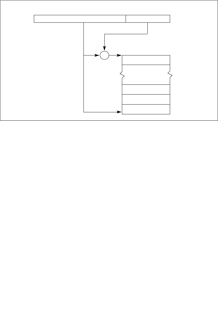
Vol. 3A 5-13
INTERRUPT AND EXCEPTION HANDLING
5.11 IDT DESCRIPTORS
The IDT may contain any of three kinds of gate descriptors:
•Task-gate descriptor
•Interrupt-gate descriptor
•Trap-gate descriptor
Figure 5-2 shows the formats for the task-gate, interrupt-gate, and trap-gate descriptors. The
format of a task gate used in an IDT is the same as that of a task gate used in the GDT or an LDT
(see Section 6.2.5, “Task-Gate Descriptor”). The task gate contains the segment selector for a
TSS for an exception and/or interrupt handler task.
Interrupt and trap gates are very similar to call gates (see Section 4.8.3, “Call Gates”). They
contain a far pointer (segment selector and offset) that the processor uses to transfer program
execution to a handler procedure in an exception- or interrupt-handler code segment. These gates
differ in the way the processor handles the IF flag in the EFLAGS register (see Section 5.12.1.2,
“Flag Usage By Exception- or Interrupt-Handler Procedure”).
Figure 5-1. Relationship of the IDTR and IDT
IDT Limit
IDT Base Address
+Interrupt
Descriptor Table (IDT)
Gate for
0
IDTR Register
Interrupt #n
Gate for
Interrupt #3
Gate for
Interrupt #2
Gate for
Interrupt #1
151647
0
31
0
8
16
(n−1)∗8
5-14 Vol. 3A
INTERRUPT AND EXCEPTION HANDLING
5.12 EXCEPTION AND INTERRUPT HANDLING
The processor handles calls to exception- and interrupt-handlers similar to the way it handles
calls with a CALL instruction to a procedure or a task. When responding to an exception or inter-
rupt, the processor uses the exception or interrupt vector as an index to a descriptor in the IDT.
If the index points to an interrupt gate or trap gate, the processor calls the exception or interrupt
handler in a manner similar to a CALL to a call gate (see Section 4.8.2, “Gate Descriptors,”
Figure 5-2. IDT Gate Descriptors
31 16 15 13
14 12 870
P
Offset 31..16 D
P
L04
31 16 15 0
Segment Selector Offset 15..0 0
011D
Interrupt Gate
DPL
Offset
P
Selector
Descriptor Privilege Level
Offset to procedure entry point
Segment Present flag
Segment Selector for destination code segment
31 16 15 13
14 12 870
PD
P
L04
31 16 15 0
TSS Segment Selector 0
1010
Task Gate
45
0 0 0
31 16 15 13
14 12 87 0
P
Offset 31..16 D
P
L04
31 16 15 0
Segment Selector Offset 15..0 0
111D
Trap Gate
45
0 0 0
Reserved
Size of gate: 1 = 32 bits; 0 = 16 bitsD
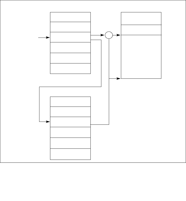
Vol. 3A 5-15
INTERRUPT AND EXCEPTION HANDLING
through Section 4.8.6, “Returning from a Called Procedure”). If index points to a task gate, the
processor executes a task switch to the exception- or interrupt-handler task in a manner similar
to a CALL to a task gate (see Section 6.3, “Task Switching”).
5.12.1 Exception- or Interrupt-Handler Procedures
An interrupt gate or trap gate references an exception- or interrupt-handler procedure that runs
in the context of the currently executing task (see Figure 5-3). The segment selector for the gate
points to a segment descriptor for an executable code segment in either the GDT or the current
LDT. The offset field of the gate descriptor points to the beginning of the exception- or interrupt-
handling procedure.
Figure 5-3. Interrupt Procedure Call
IDT
Interrupt or
Code Segment
Segment Selector
GDT or LDT
Segment
Interrupt
Vector
Base
Address
Destination
Procedure
Interrupt
+
Descriptor
Trap Gate
Offset

5-16 Vol. 3A
INTERRUPT AND EXCEPTION HANDLING
When the processor performs a call to the exception- or interrupt-handler procedure:
•If the handler procedure is going to be executed at a numerically lower privilege level, a
stack switch occurs. When the stack switch occurs:
a. The segment selector and stack pointer for the stack to be used by the handler are
obtained from the TSS for the currently executing task. On this new stack, the
processor pushes the stack segment selector and stack pointer of the interrupted
procedure.
b. The processor then saves the current state of the EFLAGS, CS, and EIP registers on
the new stack (see Figures 5-4).
c. If an exception causes an error code to be saved, it is pushed on the new stack after the
EIP value.
•If the handler procedure is going to be executed at the same privilege level as the
interrupted procedure:
a. The processor saves the current state of the EFLAGS, CS, and EIP registers on the
current stack (see Figures 5-4).
b. If an exception causes an error code to be saved, it is pushed on the current stack after
the EIP value.
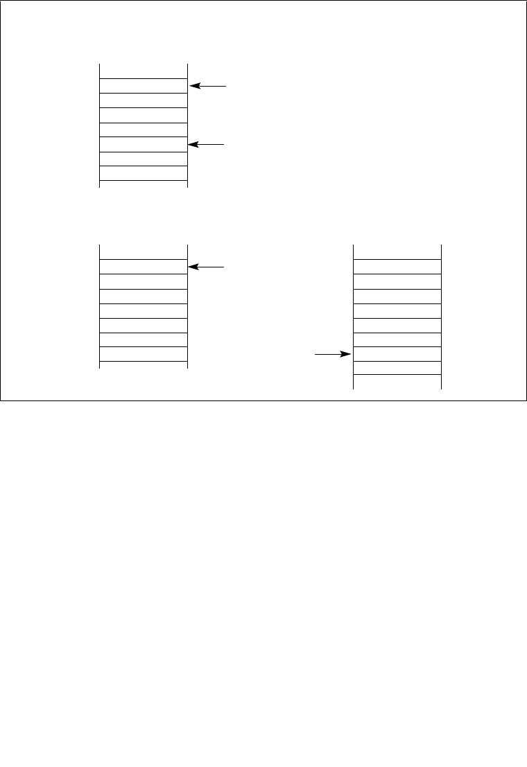
Vol. 3A 5-17
INTERRUPT AND EXCEPTION HANDLING
To return from an exception- or interrupt-handler procedure, the handler must use the IRET (or
IRETD) instruction. The IRET instruction is similar to the RET instruction except that it restores
the saved flags into the EFLAGS register. The IOPL field of the EFLAGS register is restored
only if the CPL is 0. The IF flag is changed only if the CPL is less than or equal to the IOPL.
See Chapter 3, “Instruction Set Reference, A-M,” of the IA-32 Intel® Architecture Software
Developer’s Manual, Volume 2A, for a description of the complete operation performed by the
IRET instruction.
If a stack switch occurred when calling the handler procedure, the IRET instruction switches
back to the interrupted procedure’s stack on the return.
5.12.1.1 Protection of Exception- and Interrupt-Handler Procedures
The privilege-level protection for exception- and interrupt-handler procedures is similar to that
used for ordinary procedure calls when called through a call gate (see Section 4.8.4, “Accessing
a Code Segment Through a Call Gate”). The processor does not permit transfer of execution to
an exception- or interrupt-handler procedure in a less privileged code segment (numerically
greater privilege level) than the CPL.
Figure 5-4. Stack Usage on Transfers to Interrupt and Exception-Handling Routines
CS
Error Code
EFLAGS
CS
EIP
ESP After
Transfer to Handler
Error Code
ESP Before
Transfer to Handler
EFLAGS
EIP
SS
ESP
Stack Usage with No
Privilege-Level Change
Stack Usage with
Privilege-Level Change
Interrupted Procedure’s
Interrupted Procedure’s
and Handler’s Stack
Handler’s Stack
ESP After
Transfer to Handler
Transfer to Handler
ESP Before
Stack

5-18 Vol. 3A
INTERRUPT AND EXCEPTION HANDLING
An attempt to violate this rule results in a general-protection exception (#GP). The protection
mechanism for exception- and interrupt-handler procedures is different in the following ways:
•Because interrupt and exception vectors have no RPL, the RPL is not checked on implicit
calls to exception and interrupt handlers.
•The processor checks the DPL of the interrupt or trap gate only if an exception or interrupt
is generated with an INT n, INT 3, or INTO instruction. Here, the CPL must be less than or
equal to the DPL of the gate. This restriction prevents application programs or procedures
running at privilege level 3 from using a software interrupt to access critical exception
handlers, such as the page-fault handler, providing that those handlers are placed in more
privileged code segments (numerically lower privilege level). For hardware-generated
interrupts and processor-detected exceptions, the processor ignores the DPL of interrupt
and trap gates.
Because exceptions and interrupts generally do not occur at predictable times, these privilege
rules effectively impose restrictions on the privilege levels at which exception and interrupt-
handling procedures can run. Either of the following techniques can be used to avoid privilege-
level violations.
•The exception or interrupt handler can be placed in a conforming code segment. This
technique can be used for handlers that only need to access data available on the stack (for
example, divide error exceptions). If the handler needs data from a data segment, the data
segment needs to be accessible from privilege level 3, which would make it unprotected.
•The handler can be placed in a nonconforming code segment with privilege level 0. This
handler would always run, regardless of the CPL that the interrupted program or task is
running at.
5.12.1.2 Flag Usage By Exception- or Interrupt-Handler Procedure
When accessing an exception or interrupt handler through either an interrupt gate or a trap gate,
the processor clears the TF flag in the EFLAGS register after it saves the contents of the
EFLAGS register on the stack. (On calls to exception and interrupt handlers, the processor also
clears the VM, RF, and NT flags in the EFLAGS register, after they are saved on the stack.)
Clearing the TF flag prevents instruction tracing from affecting interrupt response. A subsequent
IRET instruction restores the TF (and VM, RF, and NT) flags to the values in the saved contents
of the EFLAGS register on the stack.
The only difference between an interrupt gate and a trap gate is the way the processor handles
the IF flag in the EFLAGS register. When accessing an exception- or interrupt-handling proce-
dure through an interrupt gate, the processor clears the IF flag to prevent other interrupts from
interfering with the current interrupt handler. A subsequent IRET instruction restores the IF flag
to its value in the saved contents of the EFLAGS register on the stack. Accessing a handler
procedure through a trap gate does not affect the IF flag.

Vol. 3A 5-19
INTERRUPT AND EXCEPTION HANDLING
5.12.2 Interrupt Tasks
When an exception or interrupt handler is accessed through a task gate in the IDT, a task switch
results. Handling an exception or interrupt with a separate task offers several advantages:
•The entire context of the interrupted program or task is saved automatically.
•A new TSS permits the handler to use a new privilege level 0 stack when handling the
exception or interrupt. If an exception or interrupt occurs when the current privilege level 0
stack is corrupted, accessing the handler through a task gate can prevent a system crash by
providing the handler with a new privilege level 0 stack.
•The handler can be further isolated from other tasks by giving it a separate address space.
This is done by giving it a separate LDT.
The disadvantage of handling an interrupt with a separate task is that the amount of machine
state that must be saved on a task switch makes it slower than using an interrupt gate, resulting
in increased interrupt latency.
A task gate in the IDT references a TSS descriptor in the GDT (see Figure 5-5). A switch to the
handler task is handled in the same manner as an ordinary task switch (see Section 6.3, “Task
Switching”). The link back to the interrupted task is stored in the previous task link field of the
handler task’s TSS. If an exception caused an error code to be generated, this error code is copied
to the stack of the new task.
When exception- or interrupt-handler tasks are used in an operating system, there are actually
two mechanisms that can be used to dispatch tasks: the software scheduler (part of the operating
system) and the hardware scheduler (part of the processor's interrupt mechanism). The software
scheduler needs to accommodate interrupt tasks that may be dispatched when interrupts are
enabled.
NOTE
Because IA-32 architecture tasks are not re-entrant, an interrupt-handler task
must disable interrupts between the time it completes handling the interrupt
and the time it executes the IRET instruction. This action prevents another
interrupt from occurring while the interrupt task’s TSS is still marked busy,
which would cause a general-protection (#GP) exception.
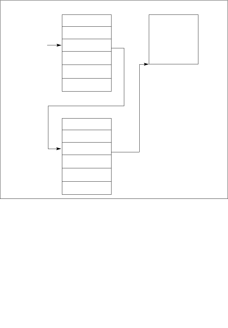
5-20 Vol. 3A
INTERRUPT AND EXCEPTION HANDLING
Figure 5-5. Interrupt Task Switch
IDT
Task Gate
TSS for Interrupt-
TSS Selector
GDT
TSS Descriptor
Interrupt
Vector
TSS
Base
Address
Handling Task
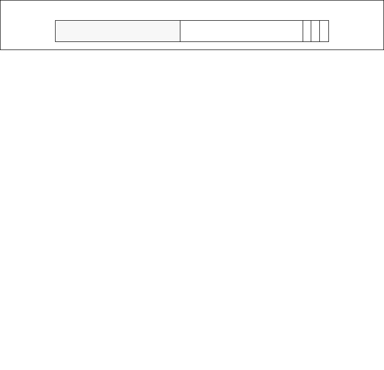
Vol. 3A 5-21
INTERRUPT AND EXCEPTION HANDLING
5.13 ERROR CODE
When an exception condition is related to a specific segment, the processor pushes an error code
onto the stack of the exception handler (whether it is a procedure or task). The error code has
the format shown in Figure 5-6. The error code resembles a segment selector; however, instead
of a TI flag and RPL field, the error code contains 3 flags:
EXT External event (bit 0) — When set, indicates that an event external to the
program, such as a hardware interrupt, caused the exception.
IDT Descriptor location (bit 1) — When set, indicates that the index portion of the
error code refers to a gate descriptor in the IDT; when clear, indicates that the
index refers to a descriptor in the GDT or the current LDT.
TI GDT/LDT (bit 2) — Only used when the IDT flag is clear. When set, the TI
flag indicates that the index portion of the error code refers to a segment or gate
descriptor in the LDT; when clear, it indicates that the index refers to a
descriptor in the current GDT.
The segment selector index field provides an index into the IDT, GDT, or current LDT to the
segment or gate selector being referenced by the error code. In some cases the error code is null
(that is, all bits in the lower word are clear). A null error code indicates that the error was not
caused by a reference to a specific segment or that a null segment descriptor was referenced in
an operation.
The format of the error code is different for page-fault exceptions (#PF). See the “Interrupt
14—Page-Fault Exception (#PF)” section in this chapter.
The error code is pushed on the stack as a doubleword or word (depending on the default inter-
rupt, trap, or task gate size). To keep the stack aligned for doubleword pushes, the upper half of
the error code is reserved. Note that the error code is not popped when the IRET instruction is
executed to return from an exception handler, so the handler must remove the error code before
executing a return.
Error codes are not pushed on the stack for exceptions that are generated externally (with the
INTR or LINT[1:0] pins) or the INT n instruction, even if an error code is normally produced
for those exceptions.
Figure 5-6. Error Code
31 0
Reserved I
D
T
T
I
123
Segment Selector Index E
X
T
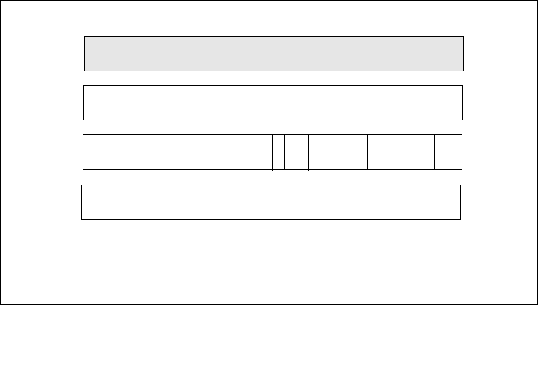
5-22 Vol. 3A
INTERRUPT AND EXCEPTION HANDLING
5.14 EXCEPTION AND INTERRUPT HANDLING IN 64-BIT MODE
In 64-bit mode, interrupt and exception handling is similar to what has been described for non-
64-bit modes. The following are the exceptions:
•All interrupt handlers pointed by the IDT are in 64-bit code (this does not apply to the SMI
handler).
•The size of interrupt-stack pushes is fixed at 64 bits; and the processor uses 8-byte, zero
extended stores.
•The stack pointer (SS:RSP) is pushed unconditionally on interrupts. In legacy modes, this
push is conditional and based on a change in current privilege level (CPL).
•The new SS is set to NULL if there is a change in CPL.
•IRET behavior changes.
•There is a new interrupt stack-switch mechanism.
•The alignment of interrupt stack frame is different.
5.14.1 64-Bit Mode IDT
Interrupt and trap gates are 16 bytes in length to provide a 64-bit offset for the instruction pointer
(RIP). The 64-bit RIP referenced by interrupt-gate descriptors allows an interrupt service routine
to be located anywhere in the linear-address space. See Figure 5-7.
Figure 5-7. 64-Bit IDT Gate Descriptors
31 16 15 13
14 12 870
P
Offset 31..16
D
P
L
04
31 16 15 0
Segment Selector Offset 15..0 0
TYPE
Interrupt/Trap Gate
DPL
Offset
P
Selector
Descriptor Privilege Level
Offset to procedure entry point
Segment Present flag
Segment Selector for destination code segment
45
0 0 0
31 0
Offset 63..32 8
31 0
12
11
IST
00
2
Reserved
IST Interrupt Stack Table

Vol. 3A 5-23
INTERRUPT AND EXCEPTION HANDLING
In 64-bit mode, the IDT index is formed by scaling the interrupt vector by 16. The first eight
bytes (bytes 7:0) of a 64-bit mode interrupt gate are similar but not identical to legacy 32-bit
interrupt gates. The type field (bits 11:8 in bytes 7:4) is described in Table 3-2. The Interrupt
Stack Table (IST) field (bits 4:0 in bytes 7:4) is used by the stack switching mechanisms
described in Section 5.14.5, “Interrupt Stack Table.” Bytes 11:8 hold the upper 32 bits of the
target RIP (interrupt segment offset) in canonical form. A general-protection exception (#GP) is
generated if software attempts to reference an interrupt gate with a target RIP that is not in
canonical form.
The target code segment referenced by the interrupt gate must be a 64-bit code segment
(CS.L = 1, CS.D = 0). If the target is not a 64-bit code segment, a general-protection exception
(#GP) is generated with the IDT vector number reported as the error code.
Only 64-bit interrupt and trap gates can be referenced in IA-32e mode (64-bit mode and compat-
ibility mode). Legacy 32-bit interrupt or trap gate types (0EH or 0FH) are redefined in IA-32e
mode as 64-bit interrupt and trap gate types. No 32-bit interrupt or trap gate type exists in IA-32e
mode. If a reference is made to a 16-bit interrupt or trap gate (06H or 07H), a general-protection
exception (#GP(0)) is generated.
5.14.2 64-Bit Mode Stack Frame
In legacy mode, the size of an IDT entry (16 bits or 32 bits) determines the size of interrupt-
stack-frame pushes. SS:ESP is pushed only on a CPL change. In 64-bit mode, the size of inter-
rupt stack-frame pushes is fixed at eight bytes. This is because only 64-bit mode gates can be
referenced. 64-bit mode also pushes SS:RSP unconditionally, rather than only on a CPL change.
Aside from error codes, pushing SS:RSP unconditionally presents operating systems with a
consistent interrupt-stackframe size across all interrupts. Interrupt service-routine entry points
that handle interrupts generated by the INTn instruction or external INTR# signal can push an
additional error code place-holder to maintain consistency.
In legacy mode, the stack pointer may be at any alignment when an interrupt or exception causes
a stack frame to be pushed. This causes the stack frame and succeeding pushes done by an inter-
rupt handler to be at arbitrary alignments. In IA-32e mode, the RSP is aligned to a 16-byte
boundary before pushing the stack frame. The stack frame itself is aligned on a 16-byte
boundary when the interrupt handler is called. The processor can arbitrarily realign the new RSP
on interrupts because the previous (possibly unaligned) RSP is unconditionally saved on the
newly aligned stack. The previous RSP will be automatically restored by a subsequent IRET.
Aligning the stack permits exception and interrupt frames to be aligned on a 16-byte boundary
before interrupts are re-enabled. This allows the stack to be formatted for optimal storage of
16-byte XMM registers, which enables the interrupt handler to use faster 16-byte aligned loads
and stores (MOVAPS rather than MOVUPS) to save and restore XMM registers.
Although the RSP alignment is always performed when LMA = 1, it is only of consequence for
the kernel-mode case where there is no stack switch or IST used. For a stack switch or IST, the
OS would have presumably put suitably aligned RSP values in the TSS.

5-24 Vol. 3A
INTERRUPT AND EXCEPTION HANDLING
5.14.3 IRET in IA-32e Mode
In IA-32e mode, IRET executes with an 8-byte operand size. There is nothing that forces this
requirement. The stack is formatted in such a way that for actions where IRET is required, the
8-byte IRET operand size works correctly.
Because interrupt stack-frame pushes are always eight bytes in IA-32e mode, an IRET must pop
eight byte items off the stack. This is accomplished by preceding the IRET with a 64-bit
operand-size prefix. The size of the pop is determined by the address size of the instruction. The
SS/ESP/RSP size adjustment is determined by the stack size.
IRET pops SS:RSP unconditionally off the interrupt stack frame only when it is executed in
64-bit mode. In compatibility mode, IRET pops SS:RSP off the stack only if there is a CPL
change. This allows legacy applications to execute properly in compatibility mode when using
the IRET instruction. 64-bit interrupt service routines that exit with an IRET unconditionally
pop SS:RSP off of the interrupt stack frame, even if the target code segment is running in 64-bit
mode or at CPL = 0. This is because the original interrupt always pushes SS:RSP.
In IA-32e mode, IRET is allowed to load a NULL SS under certain conditions. If the target mode
is 64-bit mode and the target CPL <> 3, IRET allows SS to be loaded with a NULL selector. As
part of the stack switch mechanism, an interrupt or exception sets the new SS to NULL, instead
of fetching a new SS selector from the TSS and loading the corresponding descriptor from the
GDT or LDT. The new SS selector is set to NULL in order to properly handle returns from
subsequent nested far transfers. If the called procedure itself is interrupted, the NULL SS is
pushed on the stack frame. On the subsequent IRET, the NULL SS on the stack acts as a flag to
tell the processor not to load a new SS descriptor.
5.14.4 Stack Switching in IA-32e Mode
The legacy IA-32 architecture provides a mechanism to automatically switch stack frames in
response to an interrupt. The 64-bit extensions implement a modified version of the legacy
stack-switching mechanism and an alternative stack-switching mechanism called the interrupt
stack table (IST).
In legacy modes, the legacy IA-32 stack-switch mechanism is unchanged. In IA-32e mode, the
legacy stack-switch mechanism is modified. When stacks are switched as part of a 64-bit mode
privilege-level change (resulting from an interrupt), a new SS descriptor is not loaded. IA-32e
mode loads only an inner-level RSP from the TSS. The new SS selector is forced to NULL and
the SS selector’s RPL field is set to the new CPL. The new SS is set to NULL in order to handle
nested far transfers (CALLF, INT, interrupts and exceptions). The old SS and RSP are saved on
the new stack (Figure 5-8). On the subsequent IRET, the old SS is popped from the stack and
loaded into the SS register.
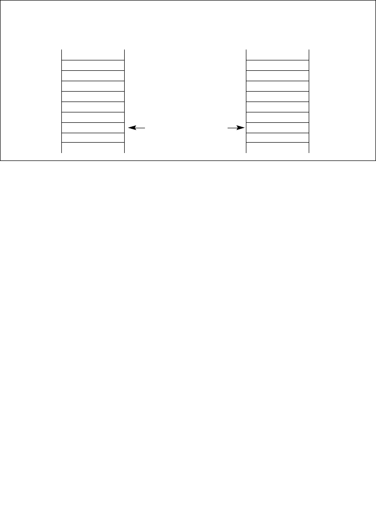
Vol. 3A 5-25
INTERRUPT AND EXCEPTION HANDLING
In summary, a stack switch in IA-32e mode works like the legacy stack switch, except that a new
SS selector is not loaded from the TSS. Instead, the new SS is forced to NULL.
5.14.5 Interrupt Stack Table
In IA-32e mode, a new interrupt stack table (IST) mechanism is available as an alternative to
the modified legacy stack-switching mechanism described above. This mechanism uncondition-
ally switches stacks when it is enabled. It can be enabled on an individual interrupt-vector basis
using a field in the IDT entry. This means that some interrupt vectors can use the modified
legacy mechanism and others can use the IST mechanism.
The IST mechanism is only available in IA-32e mode. It is part of the 64-bit mode TSS. The
motivation for the IST mechanism is to provide a method for specific interrupts (such as NMI,
double-fault, and machine-check) to always execute on a known good stack. In legacy mode,
interrupts can use the task-switch mechanism to set up a known-good stack by accessing the
interrupt service routine through a task gate located in the IDT. However, the legacy task-switch
mechanism is not supported in IA-32e mode.
Figure 5-8. IA-32e Mode Stack Usage After Privilege Level Change
CS
Error Code
EFLAGS
EIP
SS
ESP
Stack Usage with
Privilege-Level Change
Handler’s Stack
Stack Pointer After
Transfer to Handler
CS
Error Code
EFLAGS
EIP
SS
ESP
Handler’s Stack
Legacy Mode IA-32e Mode
0
+4
+8
+12
+16
+20
0
+8
+16
+24
+32
+40

5-26 Vol. 3A
INTERRUPT AND EXCEPTION HANDLING
The IST mechanism provides up to seven IST pointers in the TSS. The pointers are referenced
by an interrupt-gate descriptor in the interrupt-descriptor table (IDT); see Figure 5-7. The gate
descriptor contains a 3-bit IST index field that provides an offset into the IST section of the TSS.
Using the IST mechanism, the processor loads the value pointed by an IST pointer into the RSP.
When an interrupt occurs, the new SS selector is forced to NULL and the SS selector’s RPL field
is set to the new CPL. The old SS, RSP, RFLAGS, CS, and RIP are pushed onto the new stack.
Interrupt processing then proceeds as normal. If the IST index is zero, the modified legacy stack-
switching mechanism described above is used.
5.15 EXCEPTION AND INTERRUPT REFERENCE
The following sections describe conditions which generate exceptions and interrupts. They are
arranged in the order of vector numbers. The information contained in these sections are as
follows:
•Exception Class — Indicates whether the exception class is a fault, trap, or abort type.
Some exceptions can be either a fault or trap type, depending on when the error condition
is detected. (This section is not applicable to interrupts.)
•Description — Gives a general description of the purpose of the exception or interrupt
type. It also describes how the processor handles the exception or interrupt.
•Exception Error Code — Indicates whether an error code is saved for the exception. If
one is saved, the contents of the error code are described. (This section is not applicable to
interrupts.)
•Saved Instruction Pointer — Describes which instruction the saved (or return)
instruction pointer points to. It also indicates whether the pointer can be used to restart a
faulting instruction.
•Program State Change — Describes the effects of the exception or interrupt on the state
of the currently running program or task and the possibilities of restarting the program or
task without loss of continuity.

Vol. 3A 5-27
INTERRUPT AND EXCEPTION HANDLING
Interrupt 0—Divide Error Exception (#DE)
Exception Class Fault.
Description
Indicates the divisor operand for a DIV or IDIV instruction is 0 or that the result cannot be repre-
sented in the number of bits specified for the destination operand.
Exception Error Code
None.
Saved Instruction Pointer
Saved contents of CS and EIP registers point to the instruction that generated the exception.
Program State Change
A program-state change does not accompany the divide error, because the exception occurs
before the faulting instruction is executed.

5-28 Vol. 3A
INTERRUPT AND EXCEPTION HANDLING
Interrupt 1—Debug Exception (#DB)
Exception Class Trap or Fault. The exception handler can distinguish between traps or
faults by examining the contents of DR6 and the other debug registers.
Description
Indicates that one or more of several debug-exception conditions has been detected. Whether the
exception is a fault or a trap depends on the condition (see Table 5-3). See Chapter 18, “Debug-
ging and Performance Monitoring,” for detailed information about the debug exceptions.
Exception Error Code
None. An exception handler can examine the debug registers to determine which condition
caused the exception.
Saved Instruction Pointer
Fault — Saved contents of CS and EIP registers point to the instruction that generated the
exception.
Trap — Saved contents of CS and EIP registers point to the instruction following the instruction
that generated the exception.
Program State Change
Fault — A program-state change does not accompany the debug exception, because the excep-
tion occurs before the faulting instruction is executed. The program can resume normal execu-
tion upon returning from the debug exception handler.
Trap — A program-state change does accompany the debug exception, because the instruction
or task switch being executed is allowed to complete before the exception is generated.
However, the new state of the program is not corrupted and execution of the program can
continue reliably.
Table 5-3. Debug Exception Conditions and Corresponding Exception Classes
Exception Condition Exception Class
Instruction fetch breakpoint Fault
Data read or write breakpoint Trap
I/O read or write breakpoint Trap
General detect condition (in conjunction with in-circuit emulation) Fault
Single-step Trap
Task-switch Trap

Vol. 3A 5-29
INTERRUPT AND EXCEPTION HANDLING
Interrupt 2—NMI Interrupt
Exception Class Not applicable.
Description
The nonmaskable interrupt (NMI) is generated externally by asserting the processor’s NMI pin
or through an NMI request set by the I/O APIC to the local APIC. This interrupt causes the NMI
interrupt handler to be called.
Exception Error Code
Not applicable.
Saved Instruction Pointer
The processor always takes an NMI interrupt on an instruction boundary. The saved contents of
CS and EIP registers point to the next instruction to be executed at the point the interrupt is
taken. See Section 5.5, “Exception Classifications,” for more information about when the
processor takes NMI interrupts.
Program State Change
The instruction executing when an NMI interrupt is received is completed before the NMI is
generated. A program or task can thus be restarted upon returning from an interrupt handler
without loss of continuity, provided the interrupt handler saves the state of the processor before
handling the interrupt and restores the processor’s state prior to a return.

5-30 Vol. 3A
INTERRUPT AND EXCEPTION HANDLING
Interrupt 3—Breakpoint Exception (#BP)
Exception Class Trap.
Description
Indicates that a breakpoint instruction (INT 3) was executed, causing a breakpoint trap to be
generated. Typically, a debugger sets a breakpoint by replacing the first opcode byte of an
instruction with the opcode for the INT 3 instruction. (The INT 3 instruction is one byte long,
which makes it easy to replace an opcode in a code segment in RAM with the breakpoint
opcode.) The operating system or a debugging tool can use a data segment mapped to the same
physical address space as the code segment to place an INT 3 instruction in places where it is
desired to call the debugger.
With the P6 family, Pentium, Intel486, and Intel386 processors, it is more convenient to set
breakpoints with the debug registers. (See Section 18.3.2, “Breakpoint Exception (#BP)—Inter-
rupt Vector 3,” for information about the breakpoint exception.) If more breakpoints are needed
beyond what the debug registers allow, the INT 3 instruction can be used.
The breakpoint (#BP) exception can also be generated by executing the INT n instruction with
an operand of 3. The action of this instruction (INT 3) is slightly different than that of the INT 3
instruction (see “INTn/INTO/INT3—Call to Interrupt Procedure” in Chapter 3, “Instruction Set
Reference, A-M,” in the IA-32 Intel® Architecture Software Developer’s Manual, Volume 2A).
Exception Error Code
None.
Saved Instruction Pointer
Saved contents of CS and EIP registers point to the instruction following the INT 3 instruction.
Program State Change
Even though the EIP points to the instruction following the breakpoint instruction, the state of
the program is essentially unchanged because the INT 3 instruction does not affect any register
or memory locations. The debugger can thus resume the suspended program by replacing the
INT 3 instruction that caused the breakpoint with the original opcode and decrementing the
saved contents of the EIP register. Upon returning from the debugger, program execution
resumes with the replaced instruction.

Vol. 3A 5-31
INTERRUPT AND EXCEPTION HANDLING
Interrupt 4—Overflow Exception (#OF)
Exception Class Trap.
Description
Indicates that an overflow trap occurred when an INTO instruction was executed. The INTO
instruction checks the state of the OF flag in the EFLAGS register. If the OF flag is set, an over-
flow trap is generated.
Some arithmetic instructions (such as the ADD and SUB) perform both signed and unsigned
arithmetic. These instructions set the OF and CF flags in the EFLAGS register to indicate signed
overflow and unsigned overflow, respectively. When performing arithmetic on signed operands,
the OF flag can be tested directly or the INTO instruction can be used. The benefit of using the
INTO instruction is that if the overflow exception is detected, an exception handler can be called
automatically to handle the overflow condition.
Exception Error Code
None.
Saved Instruction Pointer
The saved contents of CS and EIP registers point to the instruction following the INTO
instruction.
Program State Change
Even though the EIP points to the instruction following the INTO instruction, the state of the
program is essentially unchanged because the INTO instruction does not affect any register or
memory locations. The program can thus resume normal execution upon returning from the
overflow exception handler.

5-32 Vol. 3A
INTERRUPT AND EXCEPTION HANDLING
Interrupt 5—BOUND Range Exceeded Exception (#BR)
Exception Class Fault.
Description
Indicates that a BOUND-range-exceeded fault occurred when a BOUND instruction was
executed. The BOUND instruction checks that a signed array index is within the upper and
lower bounds of an array located in memory. If the array index is not within the bounds of the
array, a BOUND-range-exceeded fault is generated.
Exception Error Code
None.
Saved Instruction Pointer
The saved contents of CS and EIP registers point to the BOUND instruction that generated the
exception.
Program State Change
A program-state change does not accompany the bounds-check fault, because the operands for
the BOUND instruction are not modified. Returning from the BOUND-range-exceeded excep-
tion handler causes the BOUND instruction to be restarted.

Vol. 3A 5-33
INTERRUPT AND EXCEPTION HANDLING
Interrupt 6—Invalid Opcode Exception (#UD)
Exception Class Fault.
Description
Indicates that the processor did one of the following things:
•Attempted to execute an invalid or reserved opcode.
•Attempted to execute an instruction with an operand type that is invalid for its accompa-
nying opcode; for example, the source operand for a LES instruction is not a memory
location.
•Attempted to execute an MMX or SSE/SSE2/SSE3 instruction on an IA-32 processor that
does not support the MMX technology or SSE/SSE2/SSE3 extensions, respectively.
CPUID feature flags MMX (bit 23), SSE (bit 25), SSE2 (bit 26), SSE3 (ECX, bit 0)
indicate support for these extensions.
•Attempted to execute an MMX instruction or SSE/SSE2/SSE3 SIMD instruction (with the
exception of the MOVNTI, PAUSE, PREFETCHh, SFENCE, LFENCE, MFENCE, and
CLFLUSH instructions) when the EM flag in control register CR0 is set (1).
•Attempted to execute an SSE/SE2/SSE3 instruction when the OSFXSR bit in control
register CR4 is clear (0). Note this does not include the following SSE/SSE2/SSE3 instruc-
tions: MASKMOVQ, MOVNTQ, MOVNTI, PREFETCHh, SFENCE, LFENCE,
MFENCE, and CLFLUSH; or the 64-bit versions of the PAVGB, PAVGW, PEXTRW,
PINSRW, PMAXSW, PMAXUB, PMINSW, PMINUB, PMOVMSKB, PMULHUW,
PSADBW, PSHUFW, PADDQ, and PSUBQ.
•Attempted to execute an SSE/SSE2/SSE3 instruction on an IA-32 processor that causes a
SIMD floating-point exception when the OSXMMEXCPT bit in control register CR4 is
clear (0).
•Executed a UD2 instruction. Note that even though it is the execution of the UD2
instruction that causes the invalid opcode exception, the saved instruction pointer still
points at the UD2 instruction.
•Detected a LOCK prefix that precedes an instruction that may not be locked or one that
may be locked but the destination operand is not a memory location.
•Attempted to execute an LLDT, SLDT, LTR, STR, LSL, LAR, VERR, VERW, or ARPL
instruction while in real-address or virtual-8086 mode.
•Attempted to execute the RSM instruction when not in SMM mode.
In the Pentium 4, Intel Xeon, and P6 family processors, this exception is not generated until an
attempt is made to retire the result of executing an invalid instruction; that is, decoding and spec-
ulatively attempting to execute an invalid opcode does not generate this exception. Likewise, in
the Pentium processor and earlier IA-32 processors, this exception is not generated as the result
of prefetching and preliminary decoding of an invalid instruction. (See Section 5.5, “Exception
Classifications,” for general rules for taking of interrupts and exceptions.)

5-34 Vol. 3A
INTERRUPT AND EXCEPTION HANDLING
The opcodes D6 and F1 are undefined opcodes that are reserved by the IA-32 architecture.
These opcodes, even though undefined, do not generate an invalid opcode exception.
The UD2 instruction is guaranteed to generate an invalid opcode exception.
Exception Error Code
None.
Saved Instruction Pointer
The saved contents of CS and EIP registers point to the instruction that generated the exception.
Program State Change
A program-state change does not accompany an invalid-opcode fault, because the invalid
instruction is not executed.

Vol. 3A 5-35
INTERRUPT AND EXCEPTION HANDLING
Interrupt 7—Device Not Available Exception (#NM)
Exception Class Fault.
Description
Indicates one of the following things:
The device-not-available exception is generated by either of three conditions:
•The processor executed an x87 FPU floating-point instruction while the EM flag in control
register CR0 was set (1). See the paragraph below for the special case of the WAIT/FWAIT
instruction.
•The processor executed a WAIT/FWAIT instruction while the MP and TS flags of register
CR0 were set, regardless of the setting of the EM flag.
•The processor executed an x87 FPU, MMX, or SSE/SSE2/SSE3 instruction (with the
exception of MOVNTI, PAUSE, PREFETCHh, SFENCE, LFENCE, MFENCE, and
CLFLUSH) while the TS flag in control register CR0 was set and the EM flag is clear.
The EM flag is set when the processor does not have an internal x87 FPU floating-point unit. A
device-not-available exception is then generated each time an x87 FPU floating-point instruc-
tion is encountered, allowing an exception handler to call floating-point instruction emulation
routines.
The TS flag indicates that a context switch (task switch) has occurred since the last time an x87
floating-point, MMX, or SSE/SSE2/SSE3 instruction was executed; but that the context of the
x87 FPU, XMM, and MXCSR registers were not saved. When the TS flag is set and the EM flag
is clear, the processor generates a device-not-available exception each time an x87 floating-
point, MMX, or SSE/SSE2/SSE3 instruction is encountered (with the exception of the instruc-
tions listed above). The exception handler can then save the context of the x87 FPU, XMM, and
MXCSR registers before it executes the instruction. See Section 2.5, “Control Registers,” for
more information about the TS flag.
The MP flag in control register CR0 is used along with the TS flag to determine if WAIT or
FWAIT instructions should generate a device-not-available exception. It extends the function of
the TS flag to the WAIT and FWAIT instructions, giving the exception handler an opportunity
to save the context of the x87 FPU before the WAIT or FWAIT instruction is executed. The MP
flag is provided primarily for use with the Intel 286 and Intel386 DX processors. For programs
running on the Pentium 4, Intel Xeon, P6 family, Pentium, or Intel486 DX processors, or the
Intel 487 SX coprocessors, the MP flag should always be set; for programs running on the
Intel486 SX processor, the MP flag should be clear.
Exception Error Code
None.

5-36 Vol. 3A
INTERRUPT AND EXCEPTION HANDLING
Saved Instruction Pointer
The saved contents of CS and EIP registers point to the floating-point instruction or the
WAIT/FWAIT instruction that generated the exception.
Program State Change
A program-state change does not accompany a device-not-available fault, because the instruc-
tion that generated the exception is not executed.
If the EM flag is set, the exception handler can then read the floating-point instruction pointed
to by the EIP and call the appropriate emulation routine.
If the MP and TS flags are set or the TS flag alone is set, the exception handler can save the
context of the x87 FPU, clear the TS flag, and continue execution at the interrupted floating-
point or WAIT/FWAIT instruction.

Vol. 3A 5-37
INTERRUPT AND EXCEPTION HANDLING
Interrupt 8—Double Fault Exception (#DF)
Exception Class Abort.
Description
Indicates that the processor detected a second exception while calling an exception handler for
a prior exception. Normally, when the processor detects another exception while trying to call
an exception handler, the two exceptions can be handled serially. If, however, the processor
cannot handle them serially, it signals the double-fault exception. To determine when two faults
need to be signalled as a double fault, the processor divides the exceptions into three classes:
benign exceptions, contributory exceptions, and page faults (see Table 5-4).
Table 5-5 shows the various combinations of exception classes that cause a double fault to be
generated. A double-fault exception falls in the abort class of exceptions. The program or task
cannot be restarted or resumed. The double-fault handler can be used to collect diagnostic infor-
mation about the state of the machine and/or, when possible, to shut the application and/or
system down gracefully or restart the system.
A segment or page fault may be encountered while prefetching instructions; however, this
behavior is outside the domain of Table 5-5. Any further faults generated while the processor is
attempting to transfer control to the appropriate fault handler could still lead to a double-fault
sequence.
Table 5-4. Interrupt and Exception Classes
Class Vector Number Description
Benign Exceptions and Interrupts 1
2
3
4
5
6
7
9
16
17
18
19
All
All
Debug
NMI Interrupt
Breakpoint
Overflow
BOUND Range Exceeded
Invalid Opcode
Device Not Available
Coprocessor Segment Overrun
Floating-Point Error
Alignment Check
Machine Check
SIMD floating-point
INT n
INTR
Contributory Exceptions 0
10
11
12
13
Divide Error
Invalid TSS
Segment Not Present
Stack Fault
General Protection
Page Faults 14 Page Fault

5-38 Vol. 3A
INTERRUPT AND EXCEPTION HANDLING
If another exception occurs while attempting to call the double-fault handler, the processor
enters shutdown mode. This mode is similar to the state following execution of an HLT instruc-
tion. In this mode, the processor stops executing instructions until an NMI interrupt, SMI inter-
rupt, hardware reset, or INIT# is received. The processor generates a special bus cycle to
indicate that it has entered shutdown mode. Software designers may need to be aware of the
response of hardware when it goes into shutdown mode. For example, hardware may turn on an
indicator light on the front panel, generate an NMI interrupt to record diagnostic information,
invoke reset initialization, generate an INIT initialization, or generate an SMI. If any events are
pending during shutdown, they will be handled after an wake event from shutdown is processed
(for example, A20M# interrupts).
If a shutdown occurs while the processor is executing an NMI interrupt handler, then only a
hardware reset can restart the processor. Likewise, if the shutdown occurs while executing in
SMM, a hardware reset must be used to restart the processor.
Exception Error Code
Zero. The processor always pushes an error code of 0 onto the stack of the double-fault handler.
Saved Instruction Pointer
The saved contents of CS and EIP registers are undefined.
Program State Change
A program-state following a double-fault exception is undefined. The program or task cannot
be resumed or restarted. The only available action of the double-fault exception handler is to
collect all possible context information for use in diagnostics and then close the application
and/or shut down or reset the processor.
If the double fault occurs when any portion of the exception handling machine state is corrupted,
the handler cannot be invoked and the processor must be reset.
Table 5-5. Conditions for Generating a Double Fault
Second Exception
First Exception Benign Contributory Page Fault
Benign Handle Exceptions
Serially Handle Exceptions
Serially Handle Exceptions
Serially
Contributory Handle Exceptions
Serially Generate a Double Fault Handle Exceptions
Serially
Page Fault Handle Exceptions
Serially Generate a Double Fault Generate a Double Fault

Vol. 3A 5-39
INTERRUPT AND EXCEPTION HANDLING
Interrupt 9—Coprocessor Segment Overrun
Exception Class Abort. (Intel reserved; do not use. Recent IA-32 processors do not
generate this exception.)
Description
Indicates that an Intel386 CPU-based systems with an Intel 387 math coprocessor detected a
page or segment violation while transferring the middle portion of an Intel 387 math copro-
cessor operand. The P6 family, Pentium, and Intel486 processors do not generate this exception;
instead, this condition is detected with a general protection exception (#GP), interrupt 13.
Exception Error Code
None.
Saved Instruction Pointer
The saved contents of CS and EIP registers point to the instruction that generated the exception.
Program State Change
A program-state following a coprocessor segment-overrun exception is undefined. The program
or task cannot be resumed or restarted. The only available action of the exception handler is to
save the instruction pointer and reinitialize the x87 FPU using the FNINIT instruction.

5-40 Vol. 3A
INTERRUPT AND EXCEPTION HANDLING
Interrupt 10—Invalid TSS Exception (#TS)
Exception Class Fault.
Description
Indicates that there was an error related to a TSS. Such an error might be detected during a task
switch or during the execution of instructions that use information from a TSS. Table 5-6 shows
the conditions that cause an invalid TSS exception to be generated.
Table 5-6. Invalid TSS Conditions
Error Code Index Invalid Condition
TSS segment selector index The TSS segment limit is less than 67H for 32-bit TSS or less than 2CH
for 16-bit TSS.
TSS segment selector index During an IRET task switch, the TI flag in the TSS segment selector
indicates the LDT.
TSS segment selector index During an IRET task switch, the TSS segment selector exceeds
descriptor table limit.
TSS segment selector index During an IRET task switch, the busy flag in the TSS descriptor indicates
an inactive task.
TSS segment selector index During an IRET task switch, an attempt to load the backlink limit faults.
TSS segment selector index During an IRET task switch, the backlink is a NULL selector.
TSS segment selector index During an IRET task switch, the backlink points to a descriptor which is
not a busy TSS.
TSS segment selector index The new TSS descriptor is beyond the GDT limit.
TSS segment selector index The new TSS descriptor is not writable.
TSS segment selector index Stores to the old TSS encounter a fault condition.
TSS segment selector index The old TSS descriptor is not writable for a jump or IRET task switch.
TSS segment selector index The new TSS backlink is not writable for a call or exception task switch.
TSS segment selector index The new TSS selector is null on an attempt to lock the new TSS.
TSS segment selector index The new TSS selector has the TI bit set on an attempt to lock the new
TSS.
TSS segment selector index The new TSS descriptor is not an available TSS descriptor on an
attempt to lock the new TSS.
LDT segment selector index LDT or LDT not present.
Stack segment selector index The stack segment selector exceeds descriptor table limit.
Stack segment selector index The stack segment selector is NULL.
Stack segment selector index The stack segment descriptor is a non-data segment.
Stack segment selector index The stack segment is not writable.
Stack segment selector index The stack segment DPL != CPL.
Stack segment selector index The stack segment selector RPL != CPL.

Vol. 3A 5-41
INTERRUPT AND EXCEPTION HANDLING
This exception can generated either in the context of the original task or in the context of the
new task (see Section 6.3, “Task Switching”). Until the processor has completely verified the
presence of the new TSS, the exception is generated in the context of the original task. Once the
existence of the new TSS is verified, the task switch is considered complete. Any invalid-TSS
conditions detected after this point are handled in the context of the new task. (A task switch is
considered complete when the task register is loaded with the segment selector for the new TSS
and, if the switch is due to a procedure call or interrupt, the previous task link field of the new
TSS references the old TSS.)
The invalid-TSS handler must be a task called using a task gate. Handling this exception inside
the faulting TSS context is not recommended because the processor state may not be consistent.
Code segment selector index The code segment selector exceeds descriptor table limit.
Code segment selector index The code segment selector is NULL.
Code segment selector index The code segment descriptor is not a code segment type.
Code segment selector index The nonconforming code segment DPL != CPL.
Code segment selector index The conforming code segment DPL is greater than CPL.
Data segment selector index The data segment selector exceeds the descriptor table limit.
Data segment selector index The data segment descriptor is not a readable code or data type.
Data segment selector index The data segment descriptor is a nonconforming code type and RPL >
DPL.
Data segment selector index The data segment descriptor is a nonconforming code type and CPL >
DPL.
TSS segment selector index The TSS segment selector is NULL for LTR.
TSS segment selector index The TSS segment selector has the TI bit set for LTR.
TSS segment selector index The TSS segment descriptor/upper descriptor is beyond the GDT
segment limit.
TSS segment selector index The TSS segment descriptor is not an available TSS type.
TSS segment selector index The TSS segment descriptor is an available 286 TSS type in IA-32e
mode.
TSS segment selector index The TSS segment upper descriptor is not the correct type.
TSS segment selector index The TSS segment descriptor contains a non-canonical base.
TSS segment selector index There is a limit violation in attempting to load SS selector or ESP from a
TSS on a call or exception which changes privilege levels in legacy
mode.
TSS segment selector index There is a limit violation or canonical fault in attempting to load RSP or
IST from a TSS on a call or exception which changes privilege levels in
IA-32e mode.
Table 5-6. Invalid TSS Conditions (Contd.)
Error Code Index Invalid Condition

5-42 Vol. 3A
INTERRUPT AND EXCEPTION HANDLING
Exception Error Code
An error code containing the segment selector index for the segment descriptor that caused the
violation is pushed onto the stack of the exception handler. If the EXT flag is set, it indicates that
the exception was caused by an event external to the currently running program (for example, if
an external interrupt handler using a task gate attempted a task switch to an invalid TSS).
Saved Instruction Pointer
If the exception condition was detected before the task switch was carried out, the saved
contents of CS and EIP registers point to the instruction that invoked the task switch. If the
exception condition was detected after the task switch was carried out, the saved contents of CS
and EIP registers point to the first instruction of the new task.
Program State Change
The ability of the invalid-TSS handler to recover from the fault depends on the error condition
than causes the fault. See Section 6.3, “Task Switching,” for more information on the task switch
process and the possible recovery actions that can be taken.
If an invalid TSS exception occurs during a task switch, it can occur before or after the commit-
to-new-task point. If it occurs before the commit point, no program state change occurs. If it
occurs after the commit point (when the segment descriptor information for the new segment
selectors have been loaded in the segment registers), the processor will load all the state infor-
mation from the new TSS before it generates the exception. During a task switch, the processor
first loads all the segment registers with segment selectors from the TSS, then checks their
contents for validity. If an invalid TSS exception is discovered, the remaining segment registers
are loaded but not checked for validity and therefore may not be usable for referencing memory.
The invalid TSS handler should not rely on being able to use the segment selectors found in the
CS, SS, DS, ES, FS, and GS registers without causing another exception. The exception handler
should load all segment registers before trying to resume the new task; otherwise, general-
protection exceptions (#GP) may result later under conditions that make diagnosis more difficult.
The Intel recommended way of dealing situation is to use a task for the invalid TSS exception
handler. The task switch back to the interrupted task from the invalid-TSS exception-handler task
will then cause the processor to check the registers as it loads them from the TSS.

Vol. 3A 5-43
INTERRUPT AND EXCEPTION HANDLING
Interrupt 11—Segment Not Present (#NP)
Exception Class Fault.
Description
Indicates that the present flag of a segment or gate descriptor is clear. The processor can generate
this exception during any of the following operations:
•While attempting to load CS, DS, ES, FS, or GS registers. [Detection of a not-present
segment while loading the SS register causes a stack fault exception (#SS) to be
generated.] This situation can occur while performing a task switch.
•While attempting to load the LDTR using an LLDT instruction. Detection of a not-present
LDT while loading the LDTR during a task switch operation causes an invalid-TSS
exception (#TS) to be generated.
•When executing the LTR instruction and the TSS is marked not present.
•While attempting to use a gate descriptor or TSS that is marked segment-not-present, but is
otherwise valid.
An operating system typically uses the segment-not-present exception to implement virtual
memory at the segment level. If the exception handler loads the segment and returns, the inter-
rupted program or task resumes execution.
A not-present indication in a gate descriptor, however, does not indicate that a segment is not
present (because gates do not correspond to segments). The operating system may use the
present flag for gate descriptors to trigger exceptions of special significance to the operating
system.
A contributory exception or page fault that subsequently referenced a not-present segment
would cause a double fault (#DF) to be generated instead of #NP.
Exception Error Code
An error code containing the segment selector index for the segment descriptor that caused the
violation is pushed onto the stack of the exception handler. If the EXT flag is set, it indicates that
the exception resulted from either:
•an external event (NMI or INTR) that caused an interrupt, which subsequently referenced a
not-present segment
•a benign exception that subsequently referenced a not-present segment
The IDT flag is set if the error code refers to an IDT entry. This occurs when the IDT entry for
an interrupt being serviced references a not-present gate. Such an event could be generated by
an INT instruction or a hardware interrupt.

5-44 Vol. 3A
INTERRUPT AND EXCEPTION HANDLING
Saved Instruction Pointer
The saved contents of CS and EIP registers normally point to the instruction that generated the
exception. If the exception occurred while loading segment descriptors for the segment selectors
in a new TSS, the CS and EIP registers point to the first instruction in the new task. If the excep-
tion occurred while accessing a gate descriptor, the CS and EIP registers point to the instruction
that invoked the access (for example a CALL instruction that references a call gate).
Program State Change
If the segment-not-present exception occurs as the result of loading a register (CS, DS, SS, ES,
FS, GS, or LDTR), a program-state change does accompany the exception because the register
is not loaded. Recovery from this exception is possible by simply loading the missing segment
into memory and setting the present flag in the segment descriptor.
If the segment-not-present exception occurs while accessing a gate descriptor, a program-state
change does not accompany the exception. Recovery from this exception is possible merely by
setting the present flag in the gate descriptor.
If a segment-not-present exception occurs during a task switch, it can occur before or after the
commit-to-new-task point (see Section 6.3, “Task Switching”). If it occurs before the commit
point, no program state change occurs. If it occurs after the commit point, the processor will load
all the state information from the new TSS (without performing any additional limit, present, or
type checks) before it generates the exception. The segment-not-present exception handler
should not rely on being able to use the segment selectors found in the CS, SS, DS, ES, FS, and
GS registers without causing another exception. (See the Program State Change description for
“Interrupt 10—Invalid TSS Exception (#TS)” in this chapter for additional information on how
to handle this situation.)

Vol. 3A 5-45
INTERRUPT AND EXCEPTION HANDLING
Interrupt 12—Stack Fault Exception (#SS)
Exception Class Fault.
Description
Indicates that one of the following stack related conditions was detected:
•A limit violation is detected during an operation that refers to the SS register. Operations
that can cause a limit violation include stack-oriented instructions such as POP, PUSH,
CALL, RET, IRET, ENTER, and LEAVE, as well as other memory references which
implicitly or explicitly use the SS register (for example, MOV AX, [BP+6] or MOV AX,
SS:[EAX+6]). The ENTER instruction generates this exception when there is not enough
stack space for allocating local variables.
•A not-present stack segment is detected when attempting to load the SS register. This
violation can occur during the execution of a task switch, a CALL instruction to a different
privilege level, a return to a different privilege level, an LSS instruction, or a MOV or POP
instruction to the SS register.
Recovery from this fault is possible by either extending the limit of the stack segment (in the
case of a limit violation) or loading the missing stack segment into memory (in the case of a not-
present violation.
Exception Error Code
If the exception is caused by a not-present stack segment or by overflow of the new stack during
an inter-privilege-level call, the error code contains a segment selector for the segment that
caused the exception. Here, the exception handler can test the present flag in the segment
descriptor pointed to by the segment selector to determine the cause of the exception. For a
normal limit violation (on a stack segment already in use) the error code is set to 0.
Saved Instruction Pointer
The saved contents of CS and EIP registers generally point to the instruction that generated the
exception. However, when the exception results from attempting to load a not-present stack
segment during a task switch, the CS and EIP registers point to the first instruction of the new
task.
Program State Change
A program-state change does not generally accompany a stack-fault exception, because the
instruction that generated the fault is not executed. Here, the instruction can be restarted after
the exception handler has corrected the stack fault condition.
If a stack fault occurs during a task switch, it occurs after the commit-to-new-task point (see
Section 6.3, “Task Switching”). Here, the processor loads all the state information from the new
TSS (without performing any additional limit, present, or type checks) before it generates the

5-46 Vol. 3A
INTERRUPT AND EXCEPTION HANDLING
exception. The stack fault handler should thus not rely on being able to use the segment selectors
found in the CS, SS, DS, ES, FS, and GS registers without causing another exception. The
exception handler should check all segment registers before trying to resume the new task;
otherwise, general protection faults may result later under conditions that are more difficult to
diagnose. (See the Program State Change description for “Interrupt 10—Invalid TSS Exception
(#TS)” in this chapter for additional information on how to handle this situation.)

Vol. 3A 5-47
INTERRUPT AND EXCEPTION HANDLING
Interrupt 13—General Protection Exception (#GP)
Exception Class Fault.
Description
Indicates that the processor detected one of a class of protection violations called “general-
protection violations.” The conditions that cause this exception to be generated comprise all the
protection violations that do not cause other exceptions to be generated (such as, invalid-TSS,
segment-not-present, stack-fault, or page-fault exceptions). The following conditions cause
general-protection exceptions to be generated:
•Exceeding the segment limit when accessing the CS, DS, ES, FS, or GS segments.
•Exceeding the segment limit when referencing a descriptor table (except during a task
switch or a stack switch).
•Transferring execution to a segment that is not executable.
•Writing to a code segment or a read-only data segment.
•Reading from an execute-only code segment.
•Loading the SS register with a segment selector for a read-only segment (unless the
selector comes from a TSS during a task switch, in which case an invalid-TSS exception
occurs).
•Loading the SS, DS, ES, FS, or GS register with a segment selector for a system segment.
•Loading the DS, ES, FS, or GS register with a segment selector for an execute-only code
segment.
•Loading the SS register with the segment selector of an executable segment or a null
segment selector.
•Loading the CS register with a segment selector for a data segment or a null segment
selector.
•Accessing memory using the DS, ES, FS, or GS register when it contains a null segment
selector.
•Switching to a busy task during a call or jump to a TSS.
•Using a segment selector on a non-IRET task switch that points to a TSS descriptor in the
current LDT. TSS descriptors can only reside in the GDT. This condition causes a #TS
exception during an IRET task switch.
•Violating any of the privilege rules described in Chapter 4, “Protection.”
•Exceeding the instruction length limit of 15 bytes (this only can occur when redundant
prefixes are placed before an instruction).
•Loading the CR0 register with a set PG flag (paging enabled) and a clear PE flag
(protection disabled).

5-48 Vol. 3A
INTERRUPT AND EXCEPTION HANDLING
•Loading the CR0 register with a set NW flag and a clear CD flag.
•Referencing an entry in the IDT (following an interrupt or exception) that is not an
interrupt, trap, or task gate.
•Attempting to access an interrupt or exception handler through an interrupt or trap gate
from virtual-8086 mode when the handler’s code segment DPL is greater than 0.
•Attempting to write a 1 into a reserved bit of CR4.
•Attempting to execute a privileged instruction when the CPL is not equal to 0 (see
Section 4.9, “Privileged Instructions,” for a list of privileged instructions).
•Writing to a reserved bit in an MSR.
•Accessing a gate that contains a null segment selector.
•Executing the INT n instruction when the CPL is greater than the DPL of the referenced
interrupt, trap, or task gate.
•The segment selector in a call, interrupt, or trap gate does not point to a code segment.
•The segment selector operand in the LLDT instruction is a local type (TI flag is set) or
does not point to a segment descriptor of the LDT type.
•The segment selector operand in the LTR instruction is local or points to a TSS that is not
available.
•The target code-segment selector for a call, jump, or return is null.
•If the PAE and/or PSE flag in control register CR4 is set and the processor detects any
reserved bits in a page-directory-pointer-table entry set to 1. These bits are checked during
a write to control registers CR0, CR3, or CR4 that causes a reloading of the page-
directory-pointer-table entry.
•Attempting to write a non-zero value into the reserved bits of the MXCSR register.
•Executing an SSE/SSE2/SSE3 instruction that attempts to access a 128-bit memory
location that is not aligned on a 16-byte boundary when the instruction requires 16-byte
alignment. This condition also applies to the stack segment.
A program or task can be restarted following any general-protection exception. If the exception
occurs while attempting to call an interrupt handler, the interrupted program can be restartable,
but the interrupt may be lost.
Exception Error Code
The processor pushes an error code onto the exception handler's stack. If the fault condition was
detected while loading a segment descriptor, the error code contains a segment selector to or IDT
vector number for the descriptor; otherwise, the error code is 0. The source of the selector in an
error code may be any of the following:
•An operand of the instruction.
•A selector from a gate which is the operand of the instruction.

Vol. 3A 5-49
INTERRUPT AND EXCEPTION HANDLING
•A selector from a TSS involved in a task switch.
•IDT vector number.
Saved Instruction Pointer
The saved contents of CS and EIP registers point to the instruction that generated the exception.
Program State Change
In general, a program-state change does not accompany a general-protection exception, because
the invalid instruction or operation is not executed. An exception handler can be designed to
correct all of the conditions that cause general-protection exceptions and restart the program or
task without any loss of program continuity.
If a general-protection exception occurs during a task switch, it can occur before or after the
commit-to-new-task point (see Section 6.3, “Task Switching”). If it occurs before the commit
point, no program state change occurs. If it occurs after the commit point, the processor will load
all the state information from the new TSS (without performing any additional limit, present, or
type checks) before it generates the exception. The general-protection exception handler should
thus not rely on being able to use the segment selectors found in the CS, SS, DS, ES, FS, and
GS registers without causing another exception. (See the Program State Change description for
“Interrupt 10—Invalid TSS Exception (#TS)” in this chapter for additional information on how
to handle this situation.)
General Protection Exception in 64-bit Mode
The following conditions cause general-protection exceptions in 64-bit mode:
•If the memory address is in a non-canonical form.
•If a segment descriptor memory address is in non-canonical form.
•If the target offset in a destination operand of a call or jmp is in a non-canonical form.
•If a code segment or 64-bit call gate overlaps non-canonical space.
•If the code segment descriptor pointed to by the selector in the 64-bit gate doesn't have the
L-bit set and the D-bit clear.
•If the EFLAGS.NT bit is set in IRET.
•If the stack segment selector of IRET is null when going back to compatibility mode.
•If the stack segment selector of IRET is null going back to CPL3 and 64-bit mode.
•If a null stack segment selector RPL of IRET is not equal to CPL going back to non-CPL3
and 64-bit mode.
•If the proposed new code segment descriptor of IRET has both the D-bit and the L-bit set.
•If the segment descriptor pointed to by the segment selector in the destination operand is a
code segment and it has both the D-bit and the L-bit set.

5-50 Vol. 3A
INTERRUPT AND EXCEPTION HANDLING
•If the segment descriptor from a 64-bit call gate is in non-canonical space.
•If the DPL from a 64-bit call-gate is less than the CPL or than the RPL of the 64-bit call-
gate.
•If the upper type field of a 64-bit call gate is not 0x0.
•If an attempt is made to load a null selector in the SS register in compatibility mode.
•If an attempt is made to load null selector in the SS register in CPL3 and 64-bit mode.
•If an attempt is made to load a null selector in the SS register in non-CPL3 and 64-bit mode
where RPL is not equal to CPL.
•If an attempt is made to clear CR0.PG while IA-32e mode is enabled.
•If an attempt is made to set a reserved bit in CR3, CR4 or CR8.

Vol. 3A 5-51
INTERRUPT AND EXCEPTION HANDLING
Interrupt 14—Page-Fault Exception (#PF)
Exception Class Fault.
Description
Indicates that, with paging enabled (the PG flag in the CR0 register is set), the processor detected
one of the following conditions while using the page-translation mechanism to translate a linear
address to a physical address:
•The P (present) flag in a page-directory or page-table entry needed for the address
translation is clear, indicating that a page table or the page containing the operand is not
present in physical memory.
•The procedure does not have sufficient privilege to access the indicated page (that is, a
procedure running in user mode attempts to access a supervisor-mode page).
•Code running in user mode attempts to write to a read-only page. In the Intel486 and later
processors, if the WP flag is set in CR0, the page fault will also be triggered by code
running in supervisor mode that tries to write to a read-only user-mode page.
•An instruction fetch to a linear address that translates to a physical address in a memory
page with the execute-disable bit set (for an IA-32 processor whose enhanced paging
structures support the execute disable bit, see Section 3.10, “PAE-Enabled Paging in IA-32e
Mode”).
•One or more reserved bits in page directory entry are set to 1. See description below of
RSVD error code flag.
The exception handler can recover from page-not-present conditions and restart the program or
task without any loss of program continuity. It can also restart the program or task after a privi-
lege violation, but the problem that caused the privilege violation may be uncorrectable.
Exception Error Code
Yes (special format). The processor provides the page-fault handler with two items of informa-
tion to aid in diagnosing the exception and recovering from it:
•An error code on the stack. The error code for a page fault has a format different from that
for other exceptions (see Figure 5-9). The error code tells the exception handler four
things:
— The P flag indicates whether the exception was due to a not-present page (0) or to
either an access rights violation or the use of a reserved bit (1).
— The W/R flag indicates whether the memory access that caused the exception was a
read (0) or write (1).
— The U/S flag indicates whether the processor was executing at user mode (1) or
supervisor mode (0) at the time of the exception.

5-52 Vol. 3A
INTERRUPT AND EXCEPTION HANDLING
— The RSVD flag indicates that the processor detected 1s in reserved bits of the page
directory, when the PSE or PAE flags in control register CR4 are set to 1. (The PSE
flag is only available in the Pentium 4, Intel Xeon, P6 family, and Pentium processors,
and the PAE flag is only available on the Pentium 4, Intel Xeon, and P6 family
processors. In earlier IA-32 processor, the bit position of the RSVD flag is reserved.)
— The I/D flag indicates whether the exception was caused by an instruction fetch. This
flag is reserved if the processor does not support execute-disable bit or execute disable
bit feature is not enabled (see Section 3.10).
•The contents of the CR2 register. The processor loads the CR2 register with the 32-bit
linear address that generated the exception. The page-fault handler can use this address to
locate the corresponding page directory and page-table entries. Another page fault can
potentially occur during execution of the page-fault handler; the handler should save the
contents of the CR2 register before a second page fault can occur.1 If a page fault is caused
by a page-level protection violation, the access flag in the page-directory entry is set when
the fault occurs. The behavior of IA-32 processors regarding the access flag in the corre-
sponding page-table entry is model specific and not architecturally defined.
Figure 5-9. Page-Fault Error Code
1. Processors update CR2 whenever a page fault is detected. If a second page fault occurs while an earlier
page fault is being delivered, the faulting linear address of the second fault will overwrite the contents of
CR2 (replacing the previous address). These updates to CR2 occur even if the page fault results in a
double fault or occurs during the delivery of a double fault.
The fault was caused by a non-present page.
The fault was caused by a page-level protection violation.
The access causing the fault was a read.
The access causing the fault was a write.
The access causing the fault originated when the processor
was executing in supervisor mode.
The access causing the fault originated when the processor
was executing in user mode.
31 0
Reserved
123
4
The fault was not caused by reserved bit violation.
The fault was caused by reserved bits set to 1 in a page directory.
P0
1
W/R 0
1
U/S 0
RSVD 0
1
1
I/D
I/D 0 The fault was not caused by an instruction fetch.
1The fault was caused by an instruction fetch.
P
W/R
U/S
RSVD

Vol. 3A 5-53
INTERRUPT AND EXCEPTION HANDLING
Saved Instruction Pointer
The saved contents of CS and EIP registers generally point to the instruction that generated the
exception. If the page-fault exception occurred during a task switch, the CS and EIP registers
may point to the first instruction of the new task (as described in the following “Program State
Change” section).
Program State Change
A program-state change does not normally accompany a page-fault exception, because the
instruction that causes the exception to be generated is not executed. After the page-fault excep-
tion handler has corrected the violation (for example, loaded the missing page into memory),
execution of the program or task can be resumed.
When a page-fault exception is generated during a task switch, the program-state may change,
as follows. During a task switch, a page-fault exception can occur during any of following
operations:
•While writing the state of the original task into the TSS of that task.
•While reading the GDT to locate the TSS descriptor of the new task.
•While reading the TSS of the new task.
•While reading segment descriptors associated with segment selectors from the new task.
•While reading the LDT of the new task to verify the segment registers stored in the new
TSS.
In the last two cases the exception occurs in the context of the new task. The instruction pointer
refers to the first instruction of the new task, not to the instruction which caused the task switch
(or the last instruction to be executed, in the case of an interrupt). If the design of the operating
system permits page faults to occur during task-switches, the page-fault handler should be called
through a task gate.
If a page fault occurs during a task switch, the processor will load all the state information from
the new TSS (without performing any additional limit, present, or type checks) before it gener-
ates the exception. The page-fault handler should thus not rely on being able to use the segment
selectors found in the CS, SS, DS, ES, FS, and GS registers without causing another exception.
(See the Program State Change description for “Interrupt 10—Invalid TSS Exception (#TS)” in
this chapter for additional information on how to handle this situation.)
Additional Exception-Handling Information
Special care should be taken to ensure that an exception that occurs during an explicit stack
switch does not cause the processor to use an invalid stack pointer (SS:ESP). Software written
for 16-bit IA-32 processors often use a pair of instructions to change to a new stack, for example:
MOV SS, AX
MOV SP, StackTop

5-54 Vol. 3A
INTERRUPT AND EXCEPTION HANDLING
When executing this code on one of the 32-bit IA-32 processors, it is possible to get a page fault,
general-protection fault (#GP), or alignment check fault (#AC) after the segment selector has
been loaded into the SS register but before the ESP register has been loaded. At this point, the
two parts of the stack pointer (SS and ESP) are inconsistent. The new stack segment is being
used with the old stack pointer.
The processor does not use the inconsistent stack pointer if the exception handler switches to a
well defined stack (that is, the handler is a task or a more privileged procedure). However, if the
exception handler is called at the same privilege level and from the same task, the processor will
attempt to use the inconsistent stack pointer.
In systems that handle page-fault, general-protection, or alignment check exceptions within the
faulting task (with trap or interrupt gates), software executing at the same privilege level as the
exception handler should initialize a new stack by using the LSS instruction rather than a pair
of MOV instructions, as described earlier in this note. When the exception handler is running at
privilege level 0 (the normal case), the problem is limited to procedures or tasks that run at priv-
ilege level 0, typically the kernel of the operating system.

Vol. 3A 5-55
INTERRUPT AND EXCEPTION HANDLING
Interrupt 16—x87 FPU Floating-Point Error (#MF)
Exception Class Fault.
Description
Indicates that the x87 FPU has detected a floating-point error. The NE flag in the register CR0
must be set for an interrupt 16 (floating-point error exception) to be generated. (See Section 2.5,
“Control Registers,” for a detailed description of the NE flag.)
NOTE
SIMD floating-point exceptions (#XF) are signaled through interrupt 19.
While executing x87 FPU instructions, the x87 FPU detects and reports six types of floating-
point error conditions:
•Invalid operation (#I)
— Stack overflow or underflow (#IS)
— Invalid arithmetic operation (#IA)
•Divide-by-zero (#Z)
•Denormalized operand (#D)
•Numeric overflow (#O)
•Numeric underflow (#U)
•Inexact result (precision) (#P)
Each of these error conditions represents an x87 FPU exception type, and for each of exception
type, the x87 FPU provides a flag in the x87 FPU status register and a mask bit in the x87 FPU
control register. If the x87 FPU detects a floating-point error and the mask bit for the exception
type is set, the x87 FPU handles the exception automatically by generating a predefined (default)
response and continuing program execution. The default responses have been designed to
provide a reasonable result for most floating-point applications.
If the mask for the exception is clear and the NE flag in register CR0 is set, the x87 FPU does
the following:
1. Sets the necessary flag in the FPU status register.
2. Waits until the next “waiting” x87 FPU instruction or WAIT/FWAIT instruction is
encountered in the program’s instruction stream.
3. Generates an internal error signal that cause the processor to generate a floating-point
exception (#MF).

5-56 Vol. 3A
INTERRUPT AND EXCEPTION HANDLING
Prior to executing a waiting x87 FPU instruction or the WAIT/FWAIT instruction, the x87 FPU
checks for pending x87 FPU floating-point exceptions (as described in step 2 above). Pending
x87 FPU floating-point exceptions are ignored for “non-waiting” x87 FPU instructions, which
include the FNINIT, FNCLEX, FNSTSW, FNSTSW AX, FNSTCW, FNSTENV, and FNSAVE
instructions. Pending x87 FPU exceptions are also ignored when executing the state manage-
ment instructions FXSAVE and FXRSTOR.
All of the x87 FPU floating-point error conditions can be recovered from. The x87 FPU floating-
point-error exception handler can determine the error condition that caused the exception from
the settings of the flags in the x87 FPU status word. See “Software Exception Handling” in
Chapter 8, “Programming with the x87 FPU,” in the IA-32 Intel® Architecture Software Devel-
oper’s Manual, Volume 1, for more information on handling x87 FPU floating-point exceptions.
Exception Error Code
None. The x87 FPU provides its own error information.
Saved Instruction Pointer
The saved contents of CS and EIP registers point to the floating-point or WAIT/FWAIT instruc-
tion that was about to be executed when the floating-point-error exception was generated. This
is not the faulting instruction in which the error condition was detected. The address of the
faulting instruction is contained in the x87 FPU instruction pointer register. See “x87 FPU
Instruction and Operand (Data) Pointers” in Chapter 8, “Programming with the x87 FPU,” in the
IA-32 Intel® Architecture Software Developer’s Manual, Volume 1, for more information about
information the FPU saves for use in handling floating-point-error exceptions.
Program State Change
A program-state change generally accompanies an x87 FPU floating-point exception because
the handling of the exception is delayed until the next waiting x87 FPU floating-point or
WAIT/FWAIT instruction following the faulting instruction. The x87 FPU, however, saves
sufficient information about the error condition to allow recovery from the error and re-execu-
tion of the faulting instruction if needed.
In situations where non- x87 FPU floating-point instructions depend on the results of an x87
FPU floating-point instruction, a WAIT or FWAIT instruction can be inserted in front of a
dependent instruction to force a pending x87 FPU floating-point exception to be handled before
the dependent instruction is executed. See “x87 FPU Exception Synchronization” in Chapter 8,
“Programming with the x87 FPU,” in the IA-32 Intel® Architecture Software Developer’s
Manual, Volume 1, for more information about synchronization of x87 floating-point-error
exceptions.

Vol. 3A 5-57
INTERRUPT AND EXCEPTION HANDLING
Interrupt 17—Alignment Check Exception (#AC)
Exception Class Fault.
Description
Indicates that the processor detected an unaligned memory operand when alignment checking
was enabled. Alignment checks are only carried out in data (or stack) accesses (not in code
fetches or system segment accesses). An example of an alignment-check violation is a word
stored at an odd byte address, or a doubleword stored at an address that is not an integer multiple
of 4. Table 5-7 lists the alignment requirements various data types recognized by the processor.
Note that the alignment check exception (#AC) is generated only for data types that must be
aligned on word, doubleword, and quadword boundaries. A general-protection exception (#GP)
is generated 128-bit data types that are not aligned on a 16-byte boundary.
To enable alignment checking, the following conditions must be true:
•AM flag in CR0 register is set.
•AC flag in the EFLAGS register is set.
•The CPL is 3 (protected mode or virtual-8086 mode).
Table 5-7. Alignment Requirements by Data Type
Data Type Address Must Be Divisible By
Word 2
Doubleword 4
Single-precision floating-point (32-bits) 4
Double-precision floating-point (64-bits) 8
Double extended-precision floating-point (80-bits) 8
Quadword 8
Double quadword 16
Segment Selector 2
32-bit Far Pointer 2
48-bit Far Pointer 4
32-bit Pointer 4
GDTR, IDTR, LDTR, or Task Register Contents 4
FSTENV/FLDENV Save Area 4 or 2, depending on operand size
FSAVE/FRSTOR Save Area 4 or 2, depending on operand size
Bit String 2 or 4 depending on the operand-size attribute.

5-58 Vol. 3A
INTERRUPT AND EXCEPTION HANDLING
Alignment-check exceptions (#AC) are generated only when operating at privilege level 3 (user
mode). Memory references that default to privilege level 0, such as segment descriptor loads, do
not generate alignment-check exceptions, even when caused by a memory reference made from
privilege level 3.
Storing the contents of the GDTR, IDTR, LDTR, or task register in memory while at privilege
level 3 can generate an alignment-check exception. Although application programs do not
normally store these registers, the fault can be avoided by aligning the information stored on an
even word-address.
The FXSAVE and FXRSTOR instructions save and restore a 512-byte data structure, the first
byte of which must be aligned on a 16-byte boundary. If the alignment-check exception (#AC)
is enabled when executing these instructions (and CPL is 3), a misaligned memory operand can
cause either an alignment-check exception or a general-protection exception (#GP) depending
on the IA-32 processor implementation (see “FXSAVE-Save x87 FPU, MMX, SSE, and SSE2
State” and “FXRSTOR-Restore x87 FPU, MMX, SSE, and SSE2 State” in Chapter 3, “Instruc-
tion Set Reference, A-M,” in the IA-32 Intel® Architecture Software Developer’s Manual,
Volume 2A).
The MOVUPS and MOVUPD instructions perform 128-bit unaligned loads or stores. They do
not generate general-protection exceptions (#GP) when operands are not aligned on a 16-byte
boundary. If alignment checking is enabled, alignment-check exceptions (#AC) are generated
when instructions are not aligned on an 8-byte boundary.
FSAVE and FRSTOR instructions can generate unaligned references, which can cause align-
ment-check faults. These instructions are rarely needed by application programs.
Exception Error Code
Yes (always zero).
Saved Instruction Pointer
The saved contents of CS and EIP registers point to the instruction that generated the exception.
Program State Change
A program-state change does not accompany an alignment-check fault, because the instruction
is not executed.

Vol. 3A 5-59
INTERRUPT AND EXCEPTION HANDLING
Interrupt 18—Machine-Check Exception (#MC)
Exception Class Abort.
Description
Indicates that the processor detected an internal machine error or a bus error, or that an external
agent detected a bus error. The machine-check exception is model-specific, available only on
the Pentium 4, Intel Xeon, P6 family, and Pentium processors. The implementation of the
machine-check exception is different between the Pentium 4, Intel Xeon, P6 family, and
Pentium processors, and these implementations may not be compatible with future IA-32
processors. (Use the CPUID instruction to determine whether this feature is present.)
Bus errors detected by external agents are signaled to the processor on dedicated pins: the
BINIT# and MCERR# pins on the Pentium 4, Intel Xeon, and P6 family processors and the
BUSCHK# pin on the Pentium processor. When one of these pins is enabled, asserting the pin
causes error information to be loaded into machine-check registers and a machine-check excep-
tion is generated.
The machine-check exception and machine-check architecture are discussed in detail in
Chapter 14, “Machine-Check Architecture.” Also, see the data books for the individual proces-
sors for processor-specific hardware information.
Exception Error Code
None. Error information is provide by machine-check MSRs.
Saved Instruction Pointer
For the Pentium 4 and Intel Xeon processors, the saved contents of extended machine-check
state registers are directly associated with the error that caused the machine-check exception to
be generated (see Section 14.3.1.3, “IA32_MCG_STATUS MSR,” and Section 14.3.2.5,
“IA32_MCG Extended Machine Check State MSRs”).
For the P6 family processors, if the EIPV flag in the MCG_STATUS MSR is set, the saved
contents of CS and EIP registers are directly associated with the error that caused the machine-
check exception to be generated; if the flag is clear, the saved instruction pointer may not be
associated with the error (see Section 14.3.1.3, “IA32_MCG_STATUS MSR”).
For the Pentium processor, contents of the CS and EIP registers may not be associated with the
error.

5-60 Vol. 3A
INTERRUPT AND EXCEPTION HANDLING
Program State Change
The machine-check mechanism is enabled by setting the MCE flag in control register CR4.
For the Pentium 4, Intel Xeon, P6 family, and Pentium processors, a program-state change
always accompanies a machine-check exception, and an abort class exception is generated. For
abort exceptions, information about the exception can be collected from the machine-check
MSRs, but the program cannot generally be restarted.
If the machine-check mechanism is not enabled (the MCE flag in control register CR4 is clear),
a machine-check exception causes the processor to enter the shutdown state.

Vol. 3A 5-61
INTERRUPT AND EXCEPTION HANDLING
Interrupt 19—SIMD Floating-Point Exception (#XF)
Exception Class Fault.
Description
Indicates the processor has detected an SSE/SSE2/SSE3 SIMD floating-point exception. The
appropriate status flag in the MXCSR register must be set and the particular exception
unmasked for this interrupt to be generated.
There are six classes of numeric exception conditions that can occur while executing an SSE/
SSE2/SSE3 SIMD floating-point instruction:
•Invalid operation (#I)
•Divide-by-zero (#Z)
•Denormal operand (#D)
•Numeric overflow (#O)
•Numeric underflow (#U)
•Inexact result (Precision) (#P)
The invalid operation, divide-by-zero, and denormal-operand exceptions are pre-computation
exceptions; that is, they are detected before any arithmetic operation occurs. The numeric under-
flow, numeric overflow, and inexact result exceptions are post-computational exceptions.
See "SIMD Floating-Point Exceptions", in Chapter 11, “Programming with Streaming SIMD
Extensions 2 (SSE3),” of the IA-32 Intel® Architecture Software Developer’s Manual, Volume 1,
for additional information about the SIMD floating-point exception classes.
When a SIMD floating-point exception occurs, the processor does either of the following things:
•It handles the exception automatically by producing the most reasonable result and
allowing program execution to continue undisturbed. This is the response to masked
exceptions.
•It generates a SIMD floating-point exception, which in turn invokes a software exception
handler. This is the response to unmasked exceptions.
Each of the six SIMD floating-point exception conditions has a corresponding flag bit and mask
bit in the MXCSR register. If an exception is masked (the corresponding mask bit in the MXCSR
register is set), the processor takes an appropriate automatic default action and continues with
the computation. If the exception is unmasked (the corresponding mask bit is clear) and the
operating system supports SIMD floating-point exceptions (the OSXMMEXCPT flag in control
register CR4 is set), a software exception handler is invoked through a SIMD floating-point
exception. If the exception is unmasked and the OSXMMEXCPT bit is clear (indicating that the
operating system does not support unmasked SIMD floating-point exceptions), an invalid
opcode exception (#UD) is signaled instead of a SIMD floating-point exception.

5-62 Vol. 3A
INTERRUPT AND EXCEPTION HANDLING
Note that because SIMD floating-point exceptions are precise and occur immediately, the situ-
ation does not arise where an x87 FPU instruction, a WAIT/FWAIT instruction, or another
SSE/SSE2/SSE3 instruction will catch a pending unmasked SIMD floating-point exception.
In situations where a SIMD floating-point exception occurred while the SIMD floating-point
exceptions were masked (causing the corresponding exception flag to be set) and the SIMD
floating-point exception was subsequently unmasked, then no exception is generated when the
exception is unmasked.
When SSE/SSE2/SSE3 SIMD floating-point instructions operate on packed operands (made up
of two or four sub-operands), multiple SIMD floating-point exception conditions may be
detected. If no more than one exception condition is detected for one or more sets of sub-oper-
ands, the exception flags are set for each exception condition detected. For example, an invalid
exception detected for one sub-operand will not prevent the reporting of a divide-by-zero excep-
tion for another sub-operand. However, when two or more exceptions conditions are generated
for one sub-operand, only one exception condition is reported, according to the precedences
shown in Table 5-8. This exception precedence sometimes results in the higher priority excep-
tion condition being reported and the lower priority exception conditions being ignored.
NOTES:
1. Though a QNaN this is not an exception, the handling of a QNaN operand has precedence over lower pri-
ority exceptions. For example, a QNaN divided by zero results in a QNaN, not a divide-by-zero- excep-
tion.
2. If masked, then instruction execution continues, and a lower priority exception can occur as well.
Exception Error Code
None.
Table 5-8. SIMD Floating-Point Exceptions Priority
Priority Description
1 (Highest) Invalid operation exception due to SNaN operand (or any NaN operand for maximum,
minimum, or certain compare and convert operations).
2 QNaN operand1.
3 Any other invalid operation exception not mentioned above or a divide-by-zero
exception2.
4 Denormal operand exception2.
5 Numeric overflow and underflow exceptions possibly in conjunction with the inexact
result exception2.
6 (Lowest) Inexact result exception.

Vol. 3A 5-63
INTERRUPT AND EXCEPTION HANDLING
Saved Instruction Pointer
The saved contents of CS and EIP registers point to the SSE/SSE2/SSE3 instruction that was
executed when the SIMD floating-point exception was generated. This is the faulting instruction
in which the error condition was detected.
Program State Change
A program-state change does not accompany a SIMD floating-point exception because the
handling of the exception is immediate unless the particular exception is masked. The available
state information is often sufficient to allow recovery from the error and re-execution of the
faulting instruction if needed.

5-64 Vol. 3A
INTERRUPT AND EXCEPTION HANDLING
Interrupts 32 to 255—User Defined Interrupts
Exception Class Not applicable.
Description
Indicates that the processor did one of the following things:
•Executed an INT n instruction where the instruction operand is one of the vector numbers
from 32 through 255.
•Responded to an interrupt request at the INTR pin or from the local APIC when the
interrupt vector number associated with the request is from 32 through 255.
Exception Error Code
Not applicable.
Saved Instruction Pointer
The saved contents of CS and EIP registers point to the instruction that follows the INT n
instruction or instruction following the instruction on which the INTR signal occurred.
Program State Change
A program-state change does not accompany interrupts generated by the INT n instruction or
the INTR signal. The INT n instruction generates the interrupt within the instruction stream.
When the processor receives an INTR signal, it commits all state changes for all previous
instructions before it responds to the interrupt; so, program execution can resume upon returning
from the interrupt handler.

6
Task Management

Vol. 3A 6-1
CHAPTER 6
TASK MANAGEMENT
This chapter describes the IA-32 architecture’s task management facilities. These facilities are
only available when the processor is running in protected mode.
This chapter focuses on 32-bit tasks and the 32-bit TSS structure. For information on 16-bit
tasks and the 16-bit TSS structure, see Section 6.6, “16-Bit Task-State Segment (TSS).” For
information specific to task management in 64-bit mode, see Section 6.7, “Task Management in
64-bit Mode.”
6.1 TASK MANAGEMENT OVERVIEW
A task is a unit of work that a processor can dispatch, execute, and suspend. It can be used to
execute a program, a task or process, an operating-system service utility, an interrupt or excep-
tion handler, or a kernel or executive utility.
The IA-32 architecture provides a mechanism for saving the state of a task, for dispatching tasks
for execution, and for switching from one task to another. When operating in protected mode,
all processor execution takes place from within a task. Even simple systems must define at least
one task. More complex systems can use the processor’s task management facilities to support
multitasking applications.
6.1.1 Task Structure
A task is made up of two parts: a task execution space and a task-state segment (TSS). The task
execution space consists of a code segment, a stack segment, and one or more data segments
(see Figure 6-1). If an operating system or executive uses the processor’s privilege-level protec-
tion mechanism, the task execution space also provides a separate stack for each privilege level.
The TSS specifies the segments that make up the task execution space and provides a storage
place for task state information. In multitasking systems, the TSS also provides a mechanism for
linking tasks.
A task is identified by the segment selector for its TSS. When a task is loaded into the processor
for execution, the segment selector, base address, limit, and segment descriptor attributes for the
TSS are loaded into the task register (see Section 2.4.4, “Task Register (TR)”).
If paging is implemented for the task, the base address of the page directory used by the task is
loaded into control register CR3.
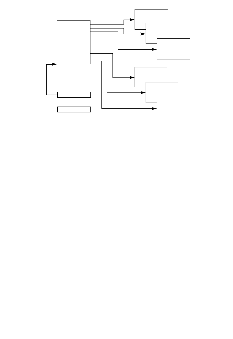
6-2 Vol. 3A
TASK MANAGEMENT
6.1.2 Task State
The following items define the state of the currently executing task:
•The task’s current execution space, defined by the segment selectors in the segment
registers (CS, DS, SS, ES, FS, and GS).
•The state of the general-purpose registers.
•The state of the EFLAGS register.
•The state of the EIP register.
•The state of control register CR3.
•The state of the task register.
•The state of the LDTR register.
•The I/O map base address and I/O map (contained in the TSS).
•Stack pointers to the privilege 0, 1, and 2 stacks (contained in the TSS).
•Link to previously executed task (contained in the TSS).
Prior to dispatching a task, all of these items are contained in the task’s TSS, except the state of
the task register. Also, the complete contents of the LDTR register are not contained in the TSS,
only the segment selector for the LDT.
Figure 6-1. Structure of a Task
Code
Segment
Stack
Segment
(Current Priv.
Data
Segment
Stack Seg.
Priv. Level 0
Stack Seg.
Priv. Level 1
Stack
Segment
(Priv. Level 2)
Task-State
Segment
(TSS)
Task Register
CR3
Level)

Vol. 3A 6-3
TASK MANAGEMENT
6.1.3 Executing a Task
Software or the processor can dispatch a task for execution in one of the following ways:
•A explicit call to a task with the CALL instruction.
•A explicit jump to a task with the JMP instruction.
•An implicit call (by the processor) to an interrupt-handler task.
•An implicit call to an exception-handler task.
•A return (initiated with an IRET instruction) when the NT flag in the EFLAGS register is
set.
All of these methods for dispatching a task identify the task to be dispatched with a segment
selector that points to a task gate or the TSS for the task. When dispatching a task with a CALL
or JMP instruction, the selector in the instruction may select the TSS directly or a task gate that
holds the selector for the TSS. When dispatching a task to handle an interrupt or exception, the
IDT entry for the interrupt or exception must contain a task gate that holds the selector for the
interrupt- or exception-handler TSS.
When a task is dispatched for execution, a task switch occurs between the currently running task
and the dispatched task. During a task switch, the execution environment of the currently
executing task (called the task’s state or context) is saved in its TSS and execution of the task is
suspended. The context for the dispatched task is then loaded into the processor and execution
of that task begins with the instruction pointed to by the newly loaded EIP register. If the task
has not been run since the system was last initialized, the EIP will point to the first instruction
of the task’s code; otherwise, it will point to the next instruction after the last instruction that the
task executed when it was last active.
If the currently executing task (the calling task) called the task being dispatched (the called task),
the TSS segment selector for the calling task is stored in the TSS of the called task to provide a
link back to the calling task.
For all IA-32 processors, tasks are not recursive. A task cannot call or jump to itself.
Interrupts and exceptions can be handled with a task switch to a handler task. Here, the processor
performs a task switch to handle the interrupt or exception and automatically switches back to
the interrupted task upon returning from the interrupt-handler task or exception-handler task.
This mechanism can also handle interrupts that occur during interrupt tasks.
As part of a task switch, the processor can also switch to another LDT, allowing each task to have
a different logical-to-physical address mapping for LDT-based segments. The page-directory base
register (CR3) also is reloaded on a task switch, allowing each task to have its own set of page
tables. These protection facilities help isolate tasks and prevent them from interfering with one
another.
If protection mechanisms are not used, the processor provides no protection between tasks. This
is true even with operating systems that use multiple privilege levels for protection. A task
running at privilege level 3 that uses the same LDT and page tables as other privilege-level-3
tasks can access code and corrupt data and the stack of other tasks.

6-4 Vol. 3A
TASK MANAGEMENT
Use of task management facilities for handling multitasking applications is optional. Multi-
tasking can be handled in software, with each software defined task executed in the context of
a single IA-32 architecture task.
6.2 TASK MANAGEMENT DATA STRUCTURES
The processor defines five data structures for handling task-related activities:
•Task-state segment (TSS).
•Task-gate descriptor.
•TSS descriptor.
•Task register.
•NT flag in the EFLAGS register.
When operating in protected mode, a TSS and TSS descriptor must be created for at least one
task, and the segment selector for the TSS must be loaded into the task register (using the LTR
instruction).
6.2.1 Task-State Segment (TSS)
The processor state information needed to restore a task is saved in a system segment called the
task-state segment (TSS). Figure 6-2 shows the format of a TSS for tasks designed for 32-bit
CPUs. The fields of a TSS are divided into two main categories: dynamic fields and static fields.
For information about 16-bit Intel 286 processor task structures, see Section 6.6, “16-Bit Task-
State Segment (TSS).” For information about 64-bit mode task structures, see Section 6.7, “Task
Management in 64-bit Mode.”
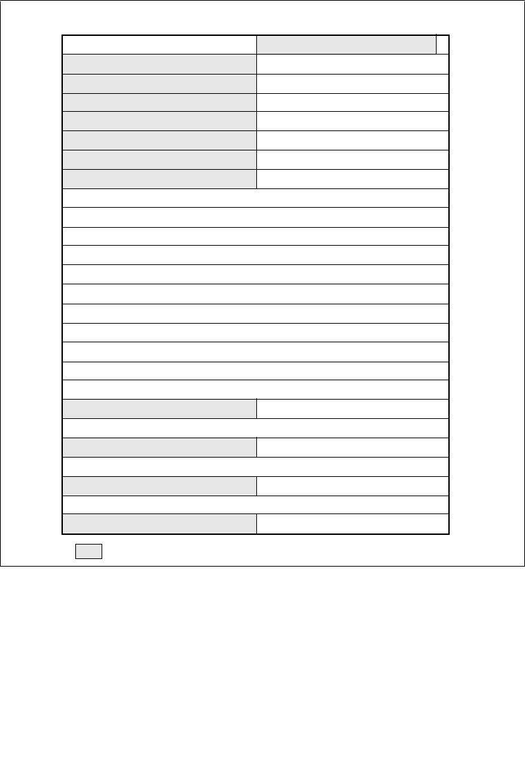
Vol. 3A 6-5
TASK MANAGEMENT
The processor updates dynamic fields when a task is suspended during a task switch. The
following are dynamic fields:
•General-purpose register fields — State of the EAX, ECX, EDX, EBX, ESP, EBP, ESI,
and EDI registers prior to the task switch.
•Segment selector fields — Segment selectors stored in the ES, CS, SS, DS, FS, and GS
registers prior to the task switch.
Figure 6-2. 32-Bit Task-State Segment (TSS)
0
31
100
96
92
88
84
80
76
I/O Map Base Address
15
LDT Segment Selector
GS
FS
DS
SS
CS
72
68
64
60
56
52
48
44
40
36
32
28
24
20
SS2
16
12
8
4
0
SS1
SS0
ESP0
Previous Task Link
ESP1
ESP2
CR3 (PDBR)
T
ES
EDI
ESI
EBP
ESP
EBX
EDX
ECX
EAX
EFLAGS
EIP
Reserved bits. Set to 0.
Reserved
Reserved
Reserved
Reserved
Reserved
Reserved
Reserved
Reserved
Reserved
Reserved
Reserved
Reserved

6-6 Vol. 3A
TASK MANAGEMENT
•EFLAGS register field — State of the EFAGS register prior to the task switch.
•EIP (instruction pointer) field — State of the EIP register prior to the task switch.
•Previous task link field — Contains the segment selector for the TSS of the previous task
(updated on a task switch that was initiated by a call, interrupt, or exception). This field
(which is sometimes called the back link field) permits a task switch back to the previous
task by using the IRET instruction.
The processor reads the static fields, but does not normally change them. These fields are set up
when a task is created. The following are static fields:
•LDT segment selector field — Contains the segment selector for the task's LDT.
•CR3 control register field — Contains the base physical address of the page directory to
be used by the task. Control register CR3 is also known as the page-directory base register
(PDBR).
•Privilege level-0, -1, and -2 stack pointer fields — These stack pointers consist of a
logical address made up of the segment selector for the stack segment (SS0, SS1, and SS2)
and an offset into the stack (ESP0, ESP1, and ESP2). Note that the values in these fields
are static for a particular task; whereas, the SS and ESP values will change if stack
switching occurs within the task.
•T (debug trap) flag (byte 100, bit 0) — When set, the T flag causes the processor to raise
a debug exception when a task switch to this task occurs (see Section 18.3.1.5, “Task-
Switch Exception Condition”).
•I/O map base address field — Contains a 16-bit offset from the base of the TSS to the I/O
permission bit map and interrupt redirection bitmap. When present, these maps are stored
in the TSS at higher addresses. The I/O map base address points to the beginning of the I/O
permission bit map and the end of the interrupt redirection bit map. See Chapter 13,
“Input/Output,” in the IA-32 Intel® Architecture Software Developer’s Manual, Volume 1,
for more information about the I/O permission bit map. See Section 15.3, “Interrupt and
Exception Handling in Virtual-8086 Mode,” for a detailed description of the interrupt
redirection bit map.
If paging is used:
•Avoid placing a page boundary in the part of the TSS that the processor reads during a task
switch (the first 104 bytes). The processor may not correctly perform address translations
if a boundary occurs in this area. During a task switch, the processor reads and writes into
the first 104 bytes of each TSS (using contiguous physical addresses beginning with the
physical address of the first byte of the TSS). So, after TSS access begins, if part of the 104
bytes is not physically contiguous, the processor will access incorrect information without
generating a page-fault exception.
•Pages corresponding to the previous task’s TSS, the current task’s TSS, and the descriptor
table entries for each all should be marked as read/write.
•Task switches are carried out faster if the pages containing these structures are present in
memory before the task switch is initiated.
Vol. 3A 6-7
TASK MANAGEMENT
6.2.2 TSS Descriptor
The TSS, like all other segments, is defined by a segment descriptor. Figure 6-3 shows the
format of a TSS descriptor. TSS descriptors may only be placed in the GDT; they cannot be
placed in an LDT or the IDT.
An attempt to access a TSS using a segment selector with its TI flag set (which indicates the
current LDT) causes a general-protection exception (#GP) to be generated during CALLs and
JMPs; it causes an invalid TSS exception (#TS) during IRETs. A general-protection exception
is also generated if an attempt is made to load a segment selector for a TSS into a segment
register.
The busy flag (B) in the type field indicates whether the task is busy. A busy task is currently
running or suspended. A type field with a value of 1001B indicates an inactive task; a value of
1011B indicates a busy task. Tasks are not recursive. The processor uses the busy flag to detect
an attempt to call a task whose execution has been interrupted. To insure that there is only one
busy flag is associated with a task, each TSS should have only one TSS descriptor that points
to it.
Figure 6-3. TSS Descriptor
31 24 23 22 21 20 19 16 15 13
14 12 11 870
P
Base 31:24 GD
P
L
Type
0
0
31 16 15 0
Base Address 15:00 Segment Limit 15:00
Base 23:16
A
V
L
Limit
19:16
0
1B01
TSS Descriptor
AVL
B
BASE
DPL
G
Available for use by system software
Busy flag
Segment Base Address
Descriptor Privilege Level
Granularity
LIMIT
P
TYPE
Segment Limit
Segment Present
Segment Type
0
4

6-8 Vol. 3A
TASK MANAGEMENT
The base, limit, and DPL fields and the granularity and present flags have functions similar to
their use in data-segment descriptors (see Section 3.4.5, “Segment Descriptors”). When the
G flag is 0 in a TSS descriptor for a 32-bit TSS, the limit field must have a value equal to or
greater than 67H, one byte less than the minimum size of a TSS. Attempting to switch to a task
whose TSS descriptor has a limit less than 67H generates an invalid-TSS exception (#TS). A
larger limit is required if an I/O permission bit map is included or if the operating system stores
additional data. The processor does not check for a limit greater than 67H on a task switch;
however, it does check when accessing the I/O permission bit map or interrupt redirection bit
map.
Any program or procedure with access to a TSS descriptor (that is, whose CPL is numerically
equal to or less than the DPL of the TSS descriptor) can dispatch the task with a call or a jump.
In most systems, the DPLs of TSS descriptors are set to values less than 3, so that only privileged
software can perform task switching. However, in multitasking applications, DPLs for some
TSS descriptors may be set to 3 to allow task switching at the application (or user) privilege
level.
6.2.3 TSS Descriptor in 64-bit mode
In 64-bit mode, task switching is not supported, but TSS descriptors still exist. The format of a
64-bit TSS is described in Section 6.7.
In 64-bit mode, the TSS descriptor is expanded to 16 bytes (see Figure 6-4 ). This expansion also
applies to an LDT descriptor in 64-bit mode. Table 3-2 provides the encoding information for
the segment type field.
Vol. 3A 6-9
TASK MANAGEMENT
6.2.4 Task Register
The task register holds the 16-bit segment selector and the entire segment descriptor (32-bit base
address, 16-bit segment limit, and descriptor attributes) for the TSS of the current task (see
Figure 2-5). This information is copied from the TSS descriptor in the GDT for the current task.
Figure 6-5 shows the path the processor uses to access the TSS (using the information in the task
register).
The task register has a visible part (that can be read and changed by software) and an invisible
part (maintained by the processor and is inaccessible by software). The segment selector in the
visible portion points to a TSS descriptor in the GDT. The processor uses the invisible portion
of the task register to cache the segment descriptor for the TSS. Caching these values in a
register makes execution of the task more efficient. The LTR (load task register) and STR (store
task register) instructions load and read the visible portion of the task register:
Figure 6-4. Format of TSS and LDT Descriptors in 64-bit Mode
31 24 23 22 21 20 19 16 15 13
14 12 11 870
P
Base 31:24 GD
P
L
Type
0
0
31 16 15 0
Base Address 15:00 Segment Limit 15:00
Base 23:16
A
V
L
Limit
19:16
0
TSS (or LDT) Descriptor
AVL
B
BASE
DPL
G
Available for use by system software
Busy flag
Segment Base Address
Descriptor Privilege Level
Granularity
LIMIT
P
TYPE
Segment Limit
Segment Present
Segment Type
0
4
31 13 12 870
Reserved
31 0
Base Address 63:32
Reserved
0
8
12
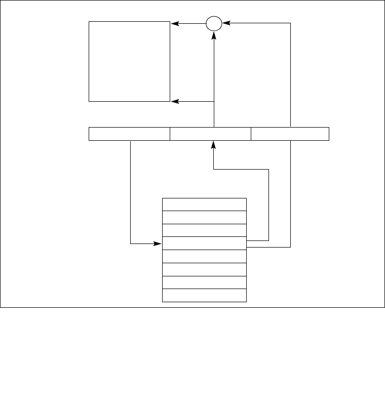
6-10 Vol. 3A
TASK MANAGEMENT
The LTR instruction loads a segment selector (source operand) into the task register that points
to a TSS descriptor in the GDT. It then loads the invisible portion of the task register with infor-
mation from the TSS descriptor. LTR is a privileged instruction that may be executed only when
the CPL is 0. It’s used during system initialization to put an initial value in the task register.
Afterwards, the contents of the task register are changed implicitly when a task switch occurs.
The STR (store task register) instruction stores the visible portion of the task register in a
general-purpose register or memory. This instruction can be executed by code running at any
privilege level in order to identify the currently running task. However, it is normally used only
by operating system software.
On power up or reset of the processor, segment selector and base address are set to the default
value of 0; the limit is set to FFFFH.
Figure 6-5. Task Register
Segment Limit
Selector
+
GDT
TSS Descriptor
0
Base Address
Task Invisible Part
Visible Part
TSS
Register
Vol. 3A 6-11
TASK MANAGEMENT
6.2.5 Task-Gate Descriptor
A task-gate descriptor provides an indirect, protected reference to a task (see Figure 6-6). It can
be placed in the GDT, an LDT, or the IDT. The TSS segment selector field in a task-gate
descriptor points to a TSS descriptor in the GDT. The RPL in this segment selector is not used.
The DPL of a task-gate descriptor controls access to the TSS descriptor during a task switch.
When a program or procedure makes a call or jump to a task through a task gate, the CPL and
the RPL field of the gate selector pointing to the task gate must be less than or equal to the DPL
of the task-gate descriptor. Note that when a task gate is used, the DPL of the destination TSS
descriptor is not used.
A task can be accessed either through a task-gate descriptor or a TSS descriptor. Both of these
structures satisfy the following needs:
•Need for a task to have only one busy flag — Because the busy flag for a task is stored in
the TSS descriptor, each task should have only one TSS descriptor. There may, however,
be several task gates that reference the same TSS descriptor.
•Need to provide selective access to tasks — Task gates fill this need, because they can
reside in an LDT and can have a DPL that is different from the TSS descriptor's DPL. A
program or procedure that does not have sufficient privilege to access the TSS descriptor
for a task in the GDT (which usually has a DPL of 0) may be allowed access to the task
through a task gate with a higher DPL. Task gates give the operating system greater
latitude for limiting access to specific tasks.
•Need for an interrupt or exception to be handled by an independent task — Task gates
may also reside in the IDT, which allows interrupts and exceptions to be handled by
handler tasks. When an interrupt or exception vector points to a task gate, the processor
switches to the specified task.
Figure 6-6. Task-Gate Descriptor
31 16 15 13
14 12 11 87 0
PD
P
L
Type
0
31 16 15 0
TSS Segment Selector
1010
DPL
P
TYPE
Descriptor Privilege Level
Segment Present
Segment Type
4
0
Reserved
Reserved
Reserved
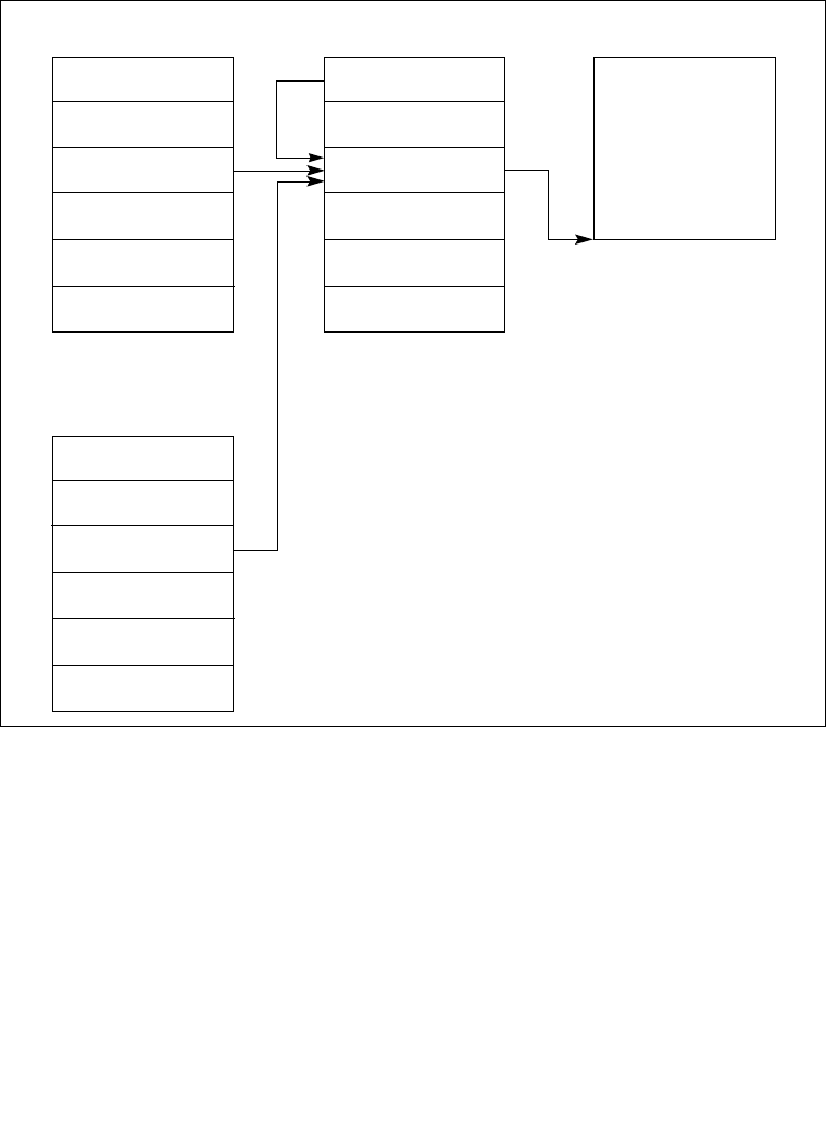
6-12 Vol. 3A
TASK MANAGEMENT
Figure 6-7 illustrates how a task gate in an LDT, a task gate in the GDT, and a task gate in the
IDT can all point to the same task.
6.3 TASK SWITCHING
The processor transfers execution to another task in one of four cases:
•The current program, task, or procedure executes a JMP or CALL instruction to a TSS
descriptor in the GDT.
•The current program, task, or procedure executes a JMP or CALL instruction to a task-gate
descriptor in the GDT or the current LDT.
•An interrupt or exception vector points to a task-gate descriptor in the IDT.
•The current task executes an IRET when the NT flag in the EFLAGS register is set.
Figure 6-7. Task Gates Referencing the Same Task
LDT
Task Gate
TSSGDT
TSS Descriptor
IDT
Task Gate
Task Gate

Vol. 3A 6-13
TASK MANAGEMENT
JMP, CALL, and IRET instructions, as well as interrupts and exceptions, are all mechanisms for
redirecting a program. The referencing of a TSS descriptor or a task gate (when calling or
jumping to a task) or the state of the NT flag (when executing an IRET instruction) determines
whether a task switch occurs.
The processor performs the following operations when switching to a new task:
1. Obtains the TSS segment selector for the new task as the operand of the JMP or CALL
instruction, from a task gate, or from the previous task link field (for a task switch initiated
with an IRET instruction).
2. Checks that the current (old) task is allowed to switch to the new task. Data-access
privilege rules apply to JMP and CALL instructions. The CPL of the current (old) task and
the RPL of the segment selector for the new task must be less than or equal to the DPL of
the TSS descriptor or task gate being referenced. Exceptions, interrupts (except for
interrupts generated by the INT n instruction), and the IRET instruction are permitted to
switch tasks regardless of the DPL of the destination task-gate or TSS descriptor. For
interrupts generated by the INT n instruction, the DPL is checked.
3. Checks that the TSS descriptor of the new task is marked present and has a valid limit
(greater than or equal to 67H).
4. Checks that the new task is available (call, jump, exception, or interrupt) or busy (IRET
return).
5. Checks that the current (old) TSS, new TSS, and all segment descriptors used in the task
switch are paged into system memory.
6. If the task switch was initiated with a JMP or IRET instruction, the processor clears the
busy (B) flag in the current (old) task’s TSS descriptor; if initiated with a CALL
instruction, an exception, or an interrupt: the busy (B) flag is left set. (See Table 6-2.)
7. If the task switch was initiated with an IRET instruction, the processor clears the NT flag
in a temporarily saved image of the EFLAGS register; if initiated with a CALL or JMP
instruction, an exception, or an interrupt, the NT flag is left unchanged in the saved
EFLAGS image.
8. Saves the state of the current (old) task in the current task’s TSS. The processor finds the
base address of the current TSS in the task register and then copies the states of the
following registers into the current TSS: all the general-purpose registers, segment
selectors from the segment registers, the temporarily saved image of the EFLAGS register,
and the instruction pointer register (EIP).
9. If the task switch was initiated with a CALL instruction, an exception, or an interrupt, the
processor will set the NT flag in the EFLAGS loaded from the new task. If initiated with an
IRET instruction or JMP instruction, the NT flag will reflect the state of NT in the
EFLAGS loaded from the new task (see Table 6-2).

6-14 Vol. 3A
TASK MANAGEMENT
10. If the task switch was initiated with a CALL instruction, JMP instruction, an exception, or
an interrupt, the processor sets the busy (B) flag in the new task’s TSS descriptor; if
initiated with an IRET instruction, the busy (B) flag is left set.
11. Loads the task register with the segment selector and descriptor for the new task's TSS.
12. The TSS state is loaded into the processor. This includes the LDTR register, the PDBR
(control register CR3), the EFLAGS registers, the EIP register, the general-purpose
registers, and the segment selectors. Note that a fault during the load of this state may
corrupt architectural state.
13. The descriptors associated with the segment selectors are loaded and qualified. Any errors
associated with this loading and qualification occur in the context of the new task.
NOTES
If all checks and saves have been carried out successfully, the processor
commits to the task switch. If an unrecoverable error occurs in steps 1
through 11, the processor does not complete the task switch and insures that
the processor is returned to its state prior to the execution of the instruction
that initiated the task switch.
If an unrecoverable error occurs in step 12, architectural state may be
corrupted, but an attempt will be made to handle the error in the prior
execution environment. If an unrecoverable error occurs after the commit
point (in step 13), the processor completes the task switch (without
performing additional access and segment availability checks) and generates
the appropriate exception prior to beginning execution of the new task.
If exceptions occur after the commit point, the exception handler must finish
the task switch itself before allowing the processor to begin executing the
new task. See Chapter 5, “Interrupt 10—Invalid TSS Exception (#TS),” for
more information about the affect of exceptions on a task when they occur
after the commit point of a task switch.
14. Begins executing the new task. (To an exception handler, the first instruction of the new
task appears not to have been executed.)
The state of the currently executing task is always saved when a successful task switch occurs.
If the task is resumed, execution starts with the instruction pointed to by the saved EIP value,
and the registers are restored to the values they held when the task was suspended.

Vol. 3A 6-15
TASK MANAGEMENT
When switching tasks, the privilege level of the new task does not inherit its privilege level from
the suspended task. The new task begins executing at the privilege level specified in the CPL
field of the CS register, which is loaded from the TSS. Because tasks are isolated by their sepa-
rate address spaces and TSSs and because privilege rules control access to a TSS, software does
not need to perform explicit privilege checks on a task switch.
Table 6-1 shows the exception conditions that the processor checks for when switching tasks. It
also shows the exception that is generated for each check if an error is detected and the segment
that the error code references. (The order of the checks in the table is the order used in the P6
family processors. The exact order is model specific and may be different for other IA-32
processors.) Exception handlers designed to handle these exceptions may be subject to recursive
calls if they attempt to reload the segment selector that generated the exception. The cause of
the exception (or the first of multiple causes) should be fixed before reloading the selector.
Table 6-1. Exception Conditions Checked During a Task Switch
Condition Checked Exception1Error Code
Reference2
Segment selector for a TSS descriptor references
the GDT and is within the limits of the table. #GP
#TS (for IRET) New Task’s TSS
TSS descriptor is present in memory. #NP New Task’s TSS
TSS descriptor is not busy (for task switch initiated by a
call, interrupt, or exception). #GP (for JMP, CALL,
INT) Task’s back-link TSS
TSS descriptor is not busy (for task switch initiated by
an IRET instruction). #TS (for IRET) New Task’s TSS
TSS segment limit greater than or equal to 108 (for 32-
bit TSS) or 44 (for 16-bit TSS). #TS New Task’s TSS
Registers are loaded from the values in the TSS.
LDT segment selector of new task is valid 3.#TS New Task’s LDT
Code segment DPL matches segment selector RPL. #TS New Code Segment
SS segment selector is valid 2.#TS New Stack Segment
Stack segment is present in memory. #SF New Stack Segment
Stack segment DPL matches CPL. #TS New stack segment
LDT of new task is present in memory. #TS New Task’s LDT
CS segment selector is valid 3.#TS New Code Segment
Code segment is present in memory. #NP New Code Segment
Stack segment DPL matches selector RPL. #TS New Stack Segment
DS, ES, FS, and GS segment selectors are valid 3.#TS New Data Segment
DS, ES, FS, and GS segments are readable. #TS New Data Segment

6-16 Vol. 3A
TASK MANAGEMENT
The TS (task switched) flag in the control register CR0 is set every time a task switch occurs.
System software uses the TS flag to coordinate the actions of floating-point unit when gener-
ating floating-point exceptions with the rest of the processor. The TS flag indicates that the
context of the floating-point unit may be different from that of the current task. See Section 2.5,
“Control Registers”, for a detailed description of the function and use of the TS flag.
6.4 TASK LINKING
The previous task link field of the TSS (sometimes called the “backlink”) and the NT flag in the
EFLAGS register are used to return execution to the previous task. EFLAGS.NT = 1 indicates
that the currently executing task is nested within the execution of another task.
When a CALL instruction, an interrupt, or an exception causes a task switch: the processor
copies the segment selector for the current TSS to the previous task link field of the TSS for the
new task; it then sets EFLAGS.NT = 1. If software uses an IRET instruction to suspend the new
task, the processor checks for EFLAGS.NT = 1; it then uses the value in the previous task link
field to return to the previous task. See Figures 6-8.
When a JMP instruction causes a task switch, the new task is not nested. The previous task link
field is not used and EFLAGS.NT = 0. Use a JMP instruction to dispatch a new task when
nesting is not desired.
DS, ES, FS, and GS segments are present in memory. #NP New Data Segment
DS, ES, FS, and GS segment DPL greater than or
equal to CPL (unless these are conforming segments). #TS New Data Segment
NOTES:
1. #NP is segment-not-present exception, #GP is general-protection exception, #TS is invalid-TSS excep-
tion, and #SF is stack-fault exception.
2. The error code contains an index to the segment descriptor referenced in this column.
3. A segment selector is valid if it is in a compatible type of table (GDT or LDT), occupies an address within
the table's segment limit, and refers to a compatible type of descriptor (for example, a segment selector
in the CS register only is valid when it points to a code-segment descriptor).
Table 6-1. Exception Conditions Checked During a Task Switch (Contd.)
Condition Checked Exception1Error Code
Reference2

Vol. 3A 6-17
TASK MANAGEMENT
Table 6-2 shows the busy flag (in the TSS segment descriptor), the NT flag, the previous task
link field, and TS flag (in control register CR0) during a task switch.
The NT flag may be modified by software executing at any privilege level. It is possible for a
program to set the NT flag and execute an IRET instruction. This might randomly invoke the
task specified in the previous link field of the current task's TSS. To keep such spurious task
switches from succeeding, the operating system should initialize the previous task link field in
every TSS that it creates to 0.
Figure 6-8. Nested Tasks
Table 6-2. Effect of a Task Switch on Busy Flag, NT Flag,
Previous Task Link Field, and TS Flag
Flag or Field Effect of JMP
instruction
Effect of CALL
Instruction or
Interrupt Effect of IRET
Instruction
Busy (B) flag of new
task. Flag is set. Must have
been clear before. Flag is set. Must have
been clear before. No change. Must have
been set.
Busy flag of old task. Flag is cleared. No change. Flag is
currently set. Flag is cleared.
NT flag of new task. Set to value from TSS of
new task. Flag is set. Set to value from TSS of
new task.
NT flag of old task. No change. No change. Flag is cleared.
Previous task link field of
new task. No change. Loaded with selector
for old task’s TSS. No change.
Previous task link field of
old task. No change. No change. No change.
TS flag in control
register CR0. Flag is set. Flag is set. Flag is set.
Top Level
Task
NT=0
Previous
TSS
Nested
Task
NT=1
TSS
More Deeply
Nested Task
NT=1
TSS
Currently Executing
Task
NT=1
EFLAGS
Task Register
Task Link Previous
Task Link Previous
Task Link

6-18 Vol. 3A
TASK MANAGEMENT
6.4.1 Use of Busy Flag To Prevent Recursive Task Switching
A TSS allows only one context to be saved for a task; therefore, once a task is called
(dispatched), a recursive (or re-entrant) call to the task would cause the current state of the task
to be lost. The busy flag in the TSS segment descriptor is provided to prevent re-entrant task
switching and a subsequent loss of task state information. The processor manages the busy flag
as follows:
1. When dispatching a task, the processor sets the busy flag of the new task.
2. If during a task switch, the current task is placed in a nested chain (the task switch is being
generated by a CALL instruction, an interrupt, or an exception), the busy flag for the
current task remains set.
3. When switching to the new task (initiated by a CALL instruction, interrupt, or exception),
the processor generates a general-protection exception (#GP) if the busy flag of the new
task is already set. If the task switch is initiated with an IRET instruction, the exception is
not raised because the processor expects the busy flag to be set.
4. When a task is terminated by a jump to a new task (initiated with a JMP instruction in the
task code) or by an IRET instruction in the task code, the processor clears the busy flag,
returning the task to the “not busy” state.
The processor prevents recursive task switching by preventing a task from switching to itself or
to any task in a nested chain of tasks. The chain of nested suspended tasks may grow to any
length, due to multiple calls, interrupts, or exceptions. The busy flag prevents a task from being
invoked if it is in this chain.
The busy flag may be used in multiprocessor configurations, because the processor follows a
LOCK protocol (on the bus or in the cache) when it sets or clears the busy flag. This lock keeps
two processors from invoking the same task at the same time. See Section 7.1.2.1, “Automatic
Locking,” for more information about setting the busy flag in a multiprocessor applications.
6.4.2 Modifying Task Linkages
In a uniprocessor system, in situations where it is necessary to remove a task from a chain of
linked tasks, use the following procedure to remove the task:
1. Disable interrupts.
2. Change the previous task link field in the TSS of the pre-empting task (the task that
suspended the task to be removed). It is assumed that the pre-empting task is the next task
(newer task) in the chain from the task to be removed. Change the previous task link field
to point to the TSS of the next oldest task in the chain or to an even older task in the chain.
3. Clear the busy (B) flag in the TSS segment descriptor for the task being removed from the
chain. If more than one task is being removed from the chain, the busy flag for each task
being remove must be cleared.
4. Enable interrupts.

Vol. 3A 6-19
TASK MANAGEMENT
In a multiprocessing system, additional synchronization and serialization operations must be
added to this procedure to insure that the TSS and its segment descriptor are both locked when
the previous task link field is changed and the busy flag is cleared.
6.5 TASK ADDRESS SPACE
The address space for a task consists of the segments that the task can access. These segments
include the code, data, stack, and system segments referenced in the TSS and any other segments
accessed by the task code. The segments are mapped into the processor’s linear address space,
which is in turn mapped into the processor’s physical address space (either directly or through
paging).
The LDT segment field in the TSS can be used to give each task its own LDT. Giving a task its
own LDT allows the task address space to be isolated from other tasks by placing the segment
descriptors for all the segments associated with the task in the task’s LDT.
It also is possible for several tasks to use the same LDT. This is a memory-efficient way to allow
specific tasks to communicate with or control each other, without dropping the protection
barriers for the entire system.
Because all tasks have access to the GDT, it also is possible to create shared segments accessed
through segment descriptors in this table.
If paging is enabled, the CR3 register (PDBR) field in the TSS allows each task to have its own
set of page tables for mapping linear addresses to physical addresses. Or, several tasks can share
the same set of page tables.
6.5.1 Mapping Tasks to the Linear and Physical Address Spaces
Tasks can be mapped to the linear address space and physical address space in one of two ways:
•One linear-to-physical address space mapping is shared among all tasks. — When
paging is not enabled, this is the only choice. Without paging, all linear addresses map to
the same physical addresses. When paging is enabled, this form of linear-to-physical
address space mapping is obtained by using one page directory for all tasks. The linear
address space may exceed the available physical space if demand-paged virtual memory is
supported.
•Each task has its own linear address space that is mapped to the physical address
space. — This form of mapping is accomplished by using a different page directory for
each task. Because the PDBR (control register CR3) is loaded on task switches, each task
may have a different page directory.
The linear address spaces of different tasks may map to completely distinct physical addresses.
If the entries of different page directories point to different page tables and the page tables point
to different pages of physical memory, then the tasks do not share physical addresses.
With either method of mapping task linear address spaces, the TSSs for all tasks must lie in a
shared area of the physical space, which is accessible to all tasks. This mapping is required so
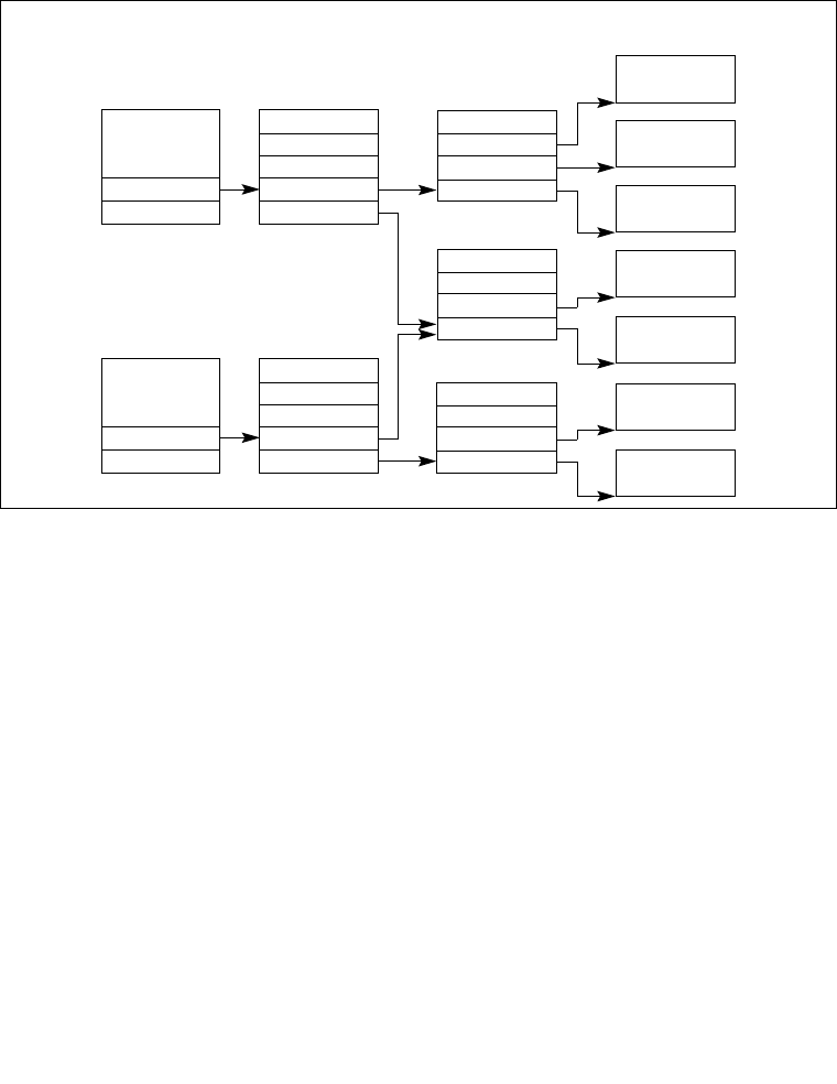
6-20 Vol. 3A
TASK MANAGEMENT
that the mapping of TSS addresses does not change while the processor is reading and updating
the TSSs during a task switch. The linear address space mapped by the GDT also should be
mapped to a shared area of the physical space; otherwise, the purpose of the GDT is defeated.
Figure 6-9 shows how the linear address spaces of two tasks can overlap in the physical space
by sharing page tables.
6.5.2 Task Logical Address Space
To allow the sharing of data among tasks, use the following techniques to create shared logical-
to-physical address-space mappings for data segments:
•Through the segment descriptors in the GDT — All tasks must have access to the
segment descriptors in the GDT. If some segment descriptors in the GDT point to segments
in the linear-address space that are mapped into an area of the physical-address space
common to all tasks, then all tasks can share the data and code in those segments.
•Through a shared LDT — Two or more tasks can use the same LDT if the LDT fields in
their TSSs point to the same LDT. If some segment descriptors in a shared LDT point to
segments that are mapped to a common area of the physical address space, the data and
code in those segments can be shared among the tasks that share the LDT. This method of
sharing is more selective than sharing through the GDT, because the sharing can be limited
to specific tasks. Other tasks in the system may have different LDTs that do not give them
access to the shared segments.
Figure 6-9. Overlapping Linear-to-Physical Mappings
Task A
Page
TSS
PDE
Page Directories
PDE
PTE
PTE
PTE
PTE
PTE
Page Tables Page Frames
Task A
Page
Task A
Page
Shared
Page
Shared
Page
Task B
Page
Task B
Page
Shared PT
PTE
PTE
PDE
PDE
PDBR
PDBR
Task A TSS
Task B TSS

Vol. 3A 6-21
TASK MANAGEMENT
•Through segment descriptors in distinct LDTs that are mapped to common addresses
in linear address space — If this common area of the linear address space is mapped to
the same area of the physical address space for each task, these segment descriptors permit
the tasks to share segments. Such segment descriptors are commonly called aliases. This
method of sharing is even more selective than those listed above, because, other segment
descriptors in the LDTs may point to independent linear addresses which are not shared.
6.6 16-BIT TASK-STATE SEGMENT (TSS)
The 32-bit IA-32 processors also recognize a 16-bit TSS format like the one used in Intel 286
processors (see Figure 6-10). This format is supported for compatibility with software written
to run on earlier IA-32 processors.
The following information is important to know about the 16-bit TSS.
•Do not use a 16-bit TSS to implement a virtual-8086 task.
•The valid segment limit for a 16-bit TSS is 2CH.
•The 16-bit TSS does not contain a field for the base address of the page directory, which is
loaded into control register CR3. A separate set of page tables for each task is not
supported for 16-bit tasks. If a 16-bit task is dispatched, the page-table structure for the
previous task is used.
•The I/O base address is not included in the 16-bit TSS. None of the functions of the I/O
map are supported.
•When task state is saved in a 16-bit TSS, the upper 16 bits of the EFLAGS register and the
EIP register are lost.
•When the general-purpose registers are loaded or saved from a 16-bit TSS, the upper 16
bits of the registers are modified and not maintained.

6-22 Vol. 3A
TASK MANAGEMENT
Figure 6-10. 16-Bit TSS Format
Task LDT Selector
DS Selector
SS Selector
CS Selector
ES Selector
DI
SI
BP
SP
BX
DX
CX
AX
FLAG Word
IP (Entry Point)
SS2
SP2
SS1
SP1
SS0
SP0
Previous Task Link
15 0
42
40
36
34
32
30
38
28
26
24
22
20
18
16
14
12
10
8
6
4
2
0

Vol. 3A 6-23
TASK MANAGEMENT
6.7 TASK MANAGEMENT IN 64-BIT MODE
In 64-bit mode, task structure and task state are similar to those in protected mode. However, the
task switching mechanism available in protected mode is not supported in 64-bit mode. Task
management and switching must be performed by software. The processor issues a general-
protection exception (#GP) if the following is attempted in 64-bit mode:
•Control transfer to a TSS or a task gate using JMP, CALL, INTn, or interrupt.
•An IRET with EFLAGS.NT (nested task) set to 1.
Although hardware task-switching is not supported in 64-bit mode, a 64-bit task state segment
(TSS) must exist. Figure 6-11 shows the format of a 64-bit TSS. The TSS holds information
important to 64-bit mode and that is not directly related to the task-switch mechanism. This
information includes:
•RSPn — The full 64-bit canonical forms of the stack pointers (RSP) for privilege levels
0-2.
•ISTn — The full 64-bit canonical forms of the interrupt stack table (IST) pointers.
•I/O map base address — The 16-bit offset to the I/O permission bit map from the 64-bit
TSS base.
The operating system must create at least one 64-bit TSS after activating IA-32e mode. It must
execute the LTR instruction (in 64-bit mode) to load the TR register with a pointer to the 64-bit
TSS responsible for both 64-bit-mode programs and compatibility-mode programs.

6-24 Vol. 3A
TASK MANAGEMENT
Figure 6-11. 64-Bit TSS Format
0
31
100
96
92
88
84
80
76
I/O Map Base Address
15
72
68
64
60
56
52
48
44
40
36
32
28
24
20
16
12
8
4
0
RSP0 (lower 32 bits)
RSP1 (lower 32 bits)
RSP2 (lower 32 bits)
Reserved bits. Set to 0.
RSP0 (upper 32 bits)
RSP1 (upper 32 bits)
RSP2 (upper 32 bits)
IST1 (lower 32 bits)
IST1 (upper 32 bits)
IST2 (lower 32 bits)
IST3 (lower 32 bits)
IST4 (lower 32 bits)
IST5 (lower 32 bits)
IST6 (lower 32 bits)
IST7 (lower 32 bits)
IST2 (upper 32 bits)
IST3 (upper 32 bits)
IST4 (upper 32 bits)
IST5 (upper 32 bits)
IST6 (upper 32 bits)
IST7 (upper 32 bits)
Reserved
Reserved
Reserved
Reserved
Reserved
Reserved

7
Multiple-Processor
Management

Vol. 3A 7-1
CHAPTER 7
MULTIPLE-PROCESSOR MANAGEMENT
The IA-32 architecture provides several mechanisms for managing and improving the perfor-
mance of multiple processors connected to the same system bus. These mechanisms include:
•Bus locking and/or cache coherency management for performing atomic operations on
system memory.
•Serializing instructions. These instructions apply only to the Pentium 4, Intel Xeon, P6
family, and Pentium processors.
•An advance programmable interrupt controller (APIC) located on the processor chip (see
Chapter 8, “Advanced Programmable Interrupt Controller (APIC)”). The APIC archi-
tecture was introduced into the IA-32 processors with the Pentium processor.
•A second-level cache (level 2, L2). For the Pentium 4, Intel Xeon, and P6 family
processors, the L2 cache is included in the processor package and is tightly coupled to the
processor. For the Pentium and Intel486 processors, pins are provided to support an
external L2 cache.
•A third-level cache (level 3, L3). For the Intel Xeon processors, the L3 cache is included in
the processor package and is tightly coupled to the processor.
•Hyper-Threading Technology, an extension to the IA-32 architecture that enables a single
processor core to execute two or more threads of execution concurrently (see Section 7.6,
“Hyper-Threading and Multi-Core Technology”).
These mechanisms are particularly useful in symmetric-multiprocessing (SMP) systems.
However, they can also be used in applications where a IA-32 processor and a special-purpose
processor (such as a communications, graphics, or video processor) share the system bus.
The goals of these multiprocessing mechanisms are:
•To maintain system memory coherency — When two or more processors are attempting
simultaneously to access the same address in system memory, some communication
mechanism or memory access protocol must be available to promote data coherency and,
in some instances, to allow one processor to temporarily lock a memory location.
•To maintain cache consistency — When one processor accesses data cached on another
processor, it must not receive incorrect data. If it modifies data, all other processors that
access that data must receive the modified data.
•To allow predictable ordering of writes to memory — In some circumstances, it is
important that memory writes be observed externally in precisely the same order as
programmed.

7-2 Vol. 3A
MULTIPLE-PROCESSOR MANAGEMENT
•To distribute interrupt handling among a group of processors — When several processors
are operating in a system in parallel, it is useful to have a centralized mechanism for
receiving interrupts and distributing them to available processors for servicing.
•To increase system performance by exploiting the multi-threaded and multi-process nature
of contemporary operating systems and applications.
The IA-32 architecture’s caching mechanism and cache consistency are discussed in Chapter 10,
“Memory Cache Control.” The APIC architecture is described in Chapter 8, “Advanced
Programmable Interrupt Controller (APIC).” Bus and memory locking, serializing instructions,
memory ordering, and Hyper-Threading Technology are discussed in the following sections.
7.1 LOCKED ATOMIC OPERATIONS
The 32-bit IA-32 processors support locked atomic operations on locations in system memory.
These operations are typically used to manage shared data structures (such as semaphores,
segment descriptors, system segments, or page tables) in which two or more processors may try
simultaneously to modify the same field or flag. The processor uses three interdependent mech-
anisms for carrying out locked atomic operations:
•Guaranteed atomic operations
•Bus locking, using the LOCK# signal and the LOCK instruction prefix
•Cache coherency protocols that insure that atomic operations can be carried out on cached
data structures (cache lock); this mechanism is present in the Pentium 4, Intel Xeon, and
P6 family processors
These mechanisms are interdependent in the following ways. Certain basic memory transactions
(such as reading or writing a byte in system memory) are always guaranteed to be handled atom-
ically. That is, once started, the processor guarantees that the operation will be completed before
another processor or bus agent is allowed access to the memory location. The processor also
supports bus locking for performing selected memory operations (such as a read-modify-write
operation in a shared area of memory) that typically need to be handled atomically, but are not
automatically handled this way. Because frequently used memory locations are often cached in
a processor’s L1 or L2 caches, atomic operations can often be carried out inside a processor’s
caches without asserting the bus lock. Here the processor’s cache coherency protocols insure
that other processors that are caching the same memory locations are managed properly while
atomic operations are performed on cached memory locations.
NOTE
Where there are contested lock accesses, software may need to implement
algorithms that ensure fair access to resources in order to prevent lock
starvation. The hardware provides no resource that guarantees fairness to
participating agents. It is the responsibility of software to manage the fairness
of semaphores and exclusive locking functions.

Vol. 3A 7-3
MULTIPLE-PROCESSOR MANAGEMENT
The mechanisms for handling locked atomic operations have evolved as the complexity of IA-32
processors has evolved. As such, more recent IA-32 processors (such as the Pentium 4, Intel
Xeon, and P6 family processors) provide a more refined locking mechanism than earlier IA-32
processors. These are described in the following sections.
7.1.1 Guaranteed Atomic Operations
The Pentium 4, Intel Xeon, P6 family, Pentium, and Intel486 processors guarantee that the
following basic memory operations will always be carried out atomically:
•Reading or writing a byte
•Reading or writing a word aligned on a 16-bit boundary
•Reading or writing a doubleword aligned on a 32-bit boundary
The Pentium 4, Intel Xeon, and P6 family, and Pentium processors guarantee that the following
additional memory operations will always be carried out atomically:
•Reading or writing a quadword aligned on a 64-bit boundary
•16-bit accesses to uncached memory locations that fit within a 32-bit data bus
The P6 family processors guarantee that the following additional memory operation will always
be carried out atomically:
•Unaligned 16-, 32-, and 64-bit accesses to cached memory that fit within a 32-byte cache
line
Accesses to cacheable memory that are split across bus widths, cache lines, and page boundaries
are not guaranteed to be atomic by the Pentium 4, Intel Xeon, P6 family, Pentium, and Intel486
processors. The Pentium 4, Intel Xeon, and P6 family processors provide bus control signals that
permit external memory subsystems to make split accesses atomic; however, nonaligned data
accesses will seriously impact the performance of the processor and should be avoided.
7.1.2 Bus Locking
IA-32 processors provide a LOCK# signal that is asserted automatically during certain critical
memory operations to lock the system bus. While this output signal is asserted, requests from
other processors or bus agents for control of the bus are blocked. Software can specify other
occasions when the LOCK semantics are to be followed by prepending the LOCK prefix to an
instruction.
In the case of the Intel386, Intel486, and Pentium processors, explicitly locked instructions will
result in the assertion of the LOCK# signal. It is the responsibility of the hardware designer to
make the LOCK# signal available in system hardware to control memory accesses among
processors.

7-4 Vol. 3A
MULTIPLE-PROCESSOR MANAGEMENT
For the Pentium 4, Intel Xeon, and P6 family processors, if the memory area being accessed is
cached internally in the processor, the LOCK# signal is generally not asserted; instead, locking
is only applied to the processor’s caches (see Section 7.1.4, “Effects of a LOCK Operation on
Internal Processor Caches”).
7.1.2.1 Automatic Locking
The operations on which the processor automatically follows the LOCK semantics are as
follows:
•When executing an XCHG instruction that references memory.
•When setting the B (busy) flag of a TSS descriptor — The processor tests and sets the
busy flag in the type field of the TSS descriptor when switching to a task. To insure that
two processors do not switch to the same task simultaneously, the processor follows the
LOCK semantics while testing and setting this flag.
•When updating segment descriptors — When loading a segment descriptor, the
processor will set the accessed flag in the segment descriptor if the flag is clear. During this
operation, the processor follows the LOCK semantics so that the descriptor will not be
modified by another processor while it is being updated. For this action to be effective,
operating-system procedures that update descriptors should use the following steps:
— Use a locked operation to modify the access-rights byte to indicate that the segment
descriptor is not-present, and specify a value for the type field that indicates that the
descriptor is being updated.
— Update the fields of the segment descriptor. (This operation may require several
memory accesses; therefore, locked operations cannot be used.)
— Use a locked operation to modify the access-rights byte to indicate that the segment
descriptor is valid and present.
The Intel386 processor always updates the accessed flag in the segment descriptor,
whether it is clear or not. The Pentium 4, Intel Xeon, P6 family, Pentium, and Intel486
processors only update this flag if it is not already set.
•When updating page-directory and page-table entries — When updating page-directory
and page-table entries, the processor uses locked cycles to set the accessed and dirty flag in
the page-directory and page-table entries.
•Acknowledging interrupts — After an interrupt request, an interrupt controller may use
the data bus to send the interrupt vector for the interrupt to the processor. The processor
follows the LOCK semantics during this time to ensure that no other data appears on the
data bus when the interrupt vector is being transmitted.

Vol. 3A 7-5
MULTIPLE-PROCESSOR MANAGEMENT
7.1.2.2 Software Controlled Bus Locking
To explicitly force the LOCK semantics, software can use the LOCK prefix with the following
instructions when they are used to modify a memory location. An invalid-opcode exception
(#UD) is generated when the LOCK prefix is used with any other instruction or when no write
operation is made to memory (that is, when the destination operand is in a register).
•The bit test and modify instructions (BTS, BTR, and BTC).
•The exchange instructions (XADD, CMPXCHG, and CMPXCHG8B).
•The LOCK prefix is automatically assumed for XCHG instruction.
•The following single-operand arithmetic and logical instructions: INC, DEC, NOT, and
NEG.
•The following two-operand arithmetic and logical instructions: ADD, ADC, SUB, SBB,
AND, OR, and XOR.
A locked instruction is guaranteed to lock only the area of memory defined by the destination
operand, but may be interpreted by the system as a lock for a larger memory area.
Software should access semaphores (shared memory used for signalling between multiple
processors) using identical addresses and operand lengths. For example, if one processor
accesses a semaphore using a word access, other processors should not access the semaphore
using a byte access. Do not use semaphores on the WC memory type.
The integrity of a bus lock is not affected by the alignment of the memory field. The LOCK
semantics are followed for as many bus cycles as necessary to update the entire operand.
However, it is recommend that locked accesses be aligned on their natural boundaries for better
system performance:
•Any boundary for an 8-bit access (locked or otherwise).
•16-bit boundary for locked word accesses.
•32-bit boundary for locked doubleword accesses.
•64-bit boundary for locked quadword accesses.
Locked operations are atomic with respect to all other memory operations and all externally
visible events. Only instruction fetch and page table accesses can pass locked instructions.
Locked instructions can be used to synchronize data written by one processor and read by
another processor.
For the P6 family processors, locked operations serialize all outstanding load and store opera-
tions (that is, wait for them to complete). This rule is also true for the Pentium 4 and Intel Xeon
processors, with one exception. Load operations that reference weakly ordered memory types
(such as the WC memory type) may not be serialized.

7-6 Vol. 3A
MULTIPLE-PROCESSOR MANAGEMENT
Locked instructions should not be used to insure that data written can be fetched as instructions.
NOTE
The locked instructions for the current versions of the Pentium 4, Intel Xeon,
P6 family, Pentium, and Intel486 processors allow data written to be fetched
as instructions. However, Intel recommends that developers who require the
use of self-modifying code use a different synchronizing mechanism,
described in the following sections.
7.1.3 Handling Self- and Cross-Modifying Code
The act of a processor writing data into a currently executing code segment with the intent of
executing that data as code is called self-modifying code. IA-32 processors exhibit model-
specific behavior when executing self-modified code, depending upon how far ahead of the
current execution pointer the code has been modified. As processor architectures become
more complex and start to speculatively execute code ahead of the retirement point (as in the
Pentium 4, Intel Xeon, and P6 family processors), the rules regarding which code should
execute, pre- or post-modification, become blurred. To write self-modifying code and ensure
that it is compliant with current and future versions of the IA-32 architecture, one of the
following two coding options must be chosen:
(* OPTION 1 *)
Store modified code (as data) into code segment;
Jump to new code or an intermediate location;
Execute new code;
(* OPTION 2 *)
Store modified code (as data) into code segment;
Execute a serializing instruction; (* For example, CPUID instruction *)
Execute new code;
(The use of one of these options is not required for programs intended to run on the Pentium or
Intel486 processors, but are recommended to insure compatibility with the Pentium 4, Intel
Xeon, and P6 family processors.)
It should be noted that self-modifying code will execute at a lower level of performance than
non-self-modifying or normal code. The degree of the performance deterioration will depend
upon the frequency of modification and specific characteristics of the code.
The act of one processor writing data into the currently executing code segment of a second
processor with the intent of having the second processor execute that data as code is called
cross-modifying code. As with self-modifying code, IA-32 processors exhibit model-specific
behavior when executing cross-modifying code, depending upon how far ahead of the executing
processors current execution pointer the code has been modified.

Vol. 3A 7-7
MULTIPLE-PROCESSOR MANAGEMENT
To write cross-modifying code and insure that it is compliant with current and future versions
of the IA-32 architecture, the following processor synchronization algorithm must be imple-
mented:
(* Action of Modifying Processor *)
Memory_Flag ← 0; (* Set Memory_Flag to value other than 1 *)
Store modified code (as data) into code segment;
Memory_Flag ← 1;
(* Action of Executing Processor *)
WHILE (Memory_Flag ≠ 1)
Wait for code to update;
ELIHW;
Execute serializing instruction; (* For example, CPUID instruction *)
Begin executing modified code;
(The use of this option is not required for programs intended to run on the Intel486 processor,
but is recommended to insure compatibility with the Pentium 4, Intel Xeon, P6 family, and
Pentium processors.)
Like self-modifying code, cross-modifying code will execute at a lower level of performance
than non-cross-modifying (normal) code, depending upon the frequency of modification and
specific characteristics of the code.
7.1.4 Effects of a LOCK Operation on Internal Processor
Caches
For the Intel486 and Pentium processors, the LOCK# signal is always asserted on the bus during
a LOCK operation, even if the area of memory being locked is cached in the processor.
For the Pentium 4, Intel Xeon, and P6 family processors, if the area of memory being locked
during a LOCK operation is cached in the processor that is performing the LOCK operation as
write-back memory and is completely contained in a cache line, the processor may not assert the
LOCK# signal on the bus. Instead, it will modify the memory location internally and allow it’s
cache coherency mechanism to insure that the operation is carried out atomically. This operation
is called “cache locking.” The cache coherency mechanism automatically prevents two or more
processors that have cached the same area of memory from simultaneously modifying data in
that area.
7.2 MEMORY ORDERING
The term memory ordering refers to the order in which the processor issues reads (loads) and
writes (stores) through the system bus to system memory. The IA-32 architecture supports
several memory ordering models depending on the implementation of the architecture. For
example, the Intel386 processor enforces program ordering (generally referred to as strong
ordering), where reads and writes are issued on the system bus in the order they occur in the
instruction stream under all circumstances.

7-8 Vol. 3A
MULTIPLE-PROCESSOR MANAGEMENT
To allow optimizing of instruction execution, the IA-32 architecture allows departures from
strong-ordering model called processor ordering in Pentium 4, Intel Xeon, and P6 family
processors. These processor-ordering variations allow performance enhancing operations such
as allowing reads to go ahead of buffered writes. The goal of any of these variations is to increase
instruction execution speeds, while maintaining memory coherency, even in multiple-processor
systems.
The following sections describe the memory ordering models used by the Intel486 and Pentium
processors, and by the Pentium 4, Intel Xeon, and P6 family processors.
7.2.1 Memory Ordering in the Intel® Pentium® and Intel486™
Processors
The Pentium and Intel486 processors follow the processor-ordered memory model; however,
they operate as strongly-ordered processors under most circumstances. Reads and writes always
appear in programmed order at the system bus—except for the following situation where
processor ordering is exhibited. Read misses are permitted to go ahead of buffered writes on the
system bus when all the buffered writes are cache hits and, therefore, are not directed to the same
address being accessed by the read miss.
In the case of I/O operations, both reads and writes always appear in programmed order.
Software intended to operate correctly in processor-ordered processors (such as the Pentium 4,
Intel Xeon, and P6 family processors) should not depend on the relatively strong ordering of
the Pentium or Intel486 processors. Instead, it should insure that accesses to shared variables
that are intended to control concurrent execution among processors are explicitly required to
obey program ordering through the use of appropriate locking or serializing operations (see
Section 7.2.4, “Strengthening or Weakening the Memory Ordering Model”).
7.2.2 Memory Ordering Pentium 4, Intel® Xeon®, and P6 Family
Processors
The Pentium 4, Intel Xeon, and P6 family processors also use a processor-ordered memory
ordering model that can be further defined as “write ordered with store-buffer forwarding.” This
model can be characterized as follows.
In a single-processor system for memory regions defined as write-back cacheable, the following
ordering rules apply:
1. Reads can be carried out speculatively and in any order.
2. Reads can pass buffered writes, but the processor is self-consistent.
3. Writes to memory are always carried out in program order, with the exception of writes
executed with the CLFLUSH instruction and streaming stores (writes) executed with the
non-temporal move instructions (MOVNTI, MOVNTQ, MOVNTDQ, MOVNTPS, and
MOVNTPD).

Vol. 3A 7-9
MULTIPLE-PROCESSOR MANAGEMENT
4. Writes can be buffered.
5. Writes are not performed speculatively; they are only performed for instructions that have
actually been retired.
6. Data from buffered writes can be forwarded to waiting reads within the processor.
7. Reads or writes cannot pass (be carried out ahead of) I/O instructions, locked instructions,
or serializing instructions.
8. Reads cannot pass LFENCE and MFENCE instructions.
9. Writes cannot pass SFENCE and MFENCE instructions.
The second rule allows a read to pass a write. However, if the write is to the same memory loca-
tion as the read, the processor’s internal “snooping” mechanism will detect the conflict and
update the cached read before the processor executes the instruction that uses the value.
The sixth rule constitutes an exception to an otherwise write ordered model. Note that the term
“write ordered with store-buffer forwarding” (introduced at the beginning of this section) refers
to the combined effects of rules 2 and 6.
In a multiple-processor system, the following ordering rules apply:
•Individual processors use the same ordering rules as in a single-processor system.
•Writes by a single processor are observed in the same order by all processors.
•Writes from the individual processors on the system bus are NOT ordered with respect to
each other.
The latter rule can be clarified by the example in Figure 7-1. Consider three processors in a
system and each processor performs three writes, one to each of three defined locations (A, B,
and C). Individually, the processors perform the writes in the same program order, but because
of bus arbitration and other memory access mechanisms, the order that the three processors write
the individual memory locations can differ each time the respective code sequences are executed
on the processors. The final values in location A, B, and C would possibly vary on each execu-
tion of the write sequence.
The processor-ordering model described in this section is virtually identical to that used by the
Pentium and Intel486 processors. The only enhancements in the Pentium 4, Intel Xeon, and P6
family processors are:
•Added support for speculative reads.
•Store-buffer forwarding, when a read passes a write to the same memory location.
•Out of order store from long string store and string move operations (see Section 7.2.3,
“Out-of-Order Stores For String Operations in Pentium 4, Intel Xeon, and P6 Family
Processors,” below).
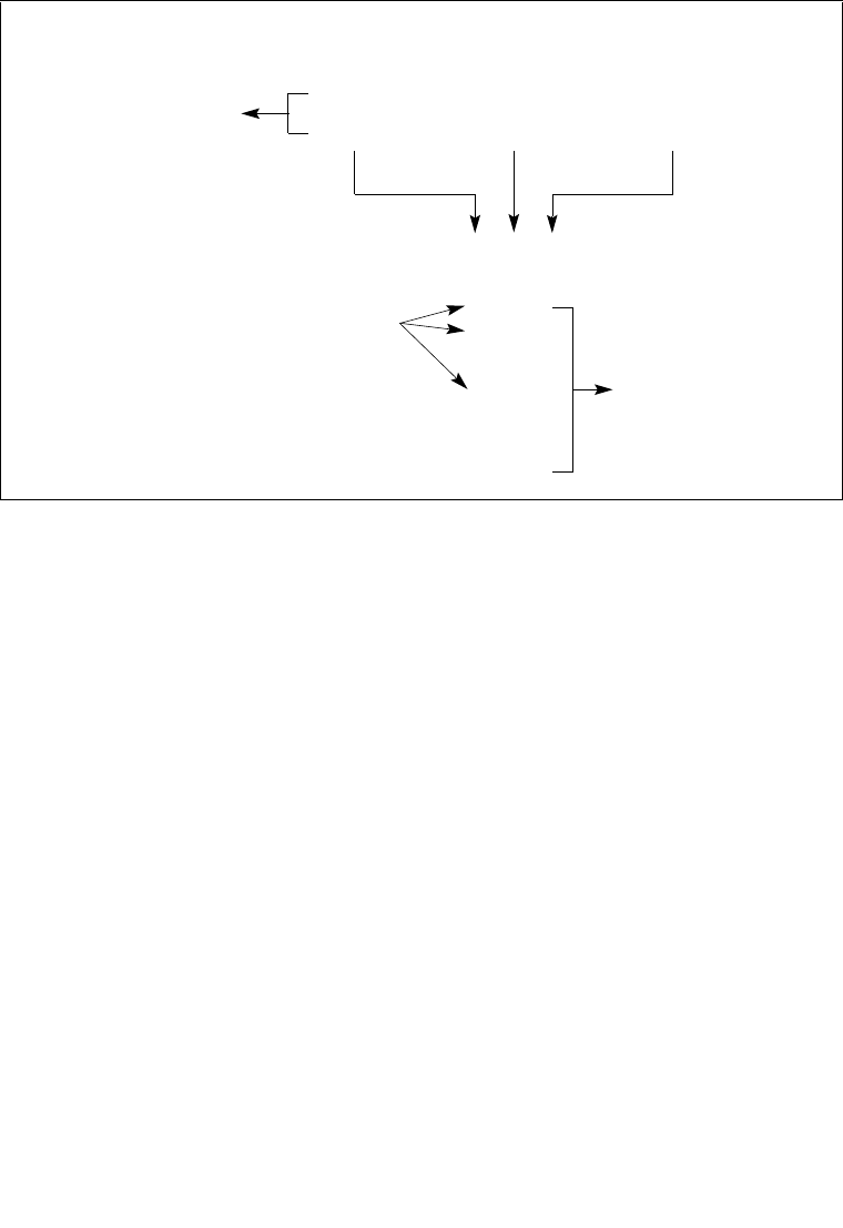
7-10 Vol. 3A
MULTIPLE-PROCESSOR MANAGEMENT
7.2.3 Out-of-Order Stores For String Operations in Pentium 4,
Intel Xeon, and P6 Family Processors
The Pentium 4, Intel Xeon, and P6 family processors modify the processors operation during the
string store operations (initiated with the MOVS and STOS instructions) to maximize perfor-
mance. Once the “fast string” operations initial conditions are met (as described below), the
processor will essentially operate on, from an external perspective, the string in a cache line by
cache line mode. This results in the processor looping on issuing a cache-line read for the source
address and an invalidation on the external bus for the destination address, knowing that all
bytes in the destination cache line will be modified, for the length of the string. In this mode
interrupts will only be accepted by the processor on cache line boundaries. It is possible in this
mode that the destination line invalidations, and therefore stores, will be issued on the external
bus out of order.
Code dependent upon sequential store ordering should not use the string operations for the entire
data structure to be stored. Data and semaphores should be separated. Order dependent code
should use a discrete semaphore uniquely stored to after any string operations to allow correctly
ordered data to be seen by all processors.
Initial conditions for “fast string” operations:
•EDI and ESI must be 8-byte aligned for the Pentium III processor. EDI must be 8-byte
aligned for the Pentium 4 processor.
•String operation must be performed in ascending address order.
Figure 7-1. Example of Write Ordering in Multiple-Processor Systems
Processor #1 Processor #2 Processor #3
Write A.3
Write B.3
Write C.3
Write A.1
Write B.1
Write A.2
Write A.3
Write C.1
Write B.2
Write C.2
Write B.3
Write C.3
Order of Writes From Individual Processors
Write A.2
Write B.2
Write C.2
Write A.1
Write B.1
Write C.1
Writes from all
processors are
not guaranteed
to occur in a
particular order.
Each processor
is guaranteed to
perform writes in
program order.
Writes are in order
with respect to
individual processes.
Example of order of actual writes
from all processors to memory

Vol. 3A 7-11
MULTIPLE-PROCESSOR MANAGEMENT
•The initial operation counter (ECX) must be equal to or greater than 64.
•Source and destination must not overlap by less than a cache line (64 bytes, Pentium 4 and
Intel Xeon processors; 32 bytes P6 family and Pentium processors).
•The memory type for both source and destination addresses must be either WB or WC.
7.2.4 Strengthening or Weakening the Memory Ordering Model
The IA-32 architecture provides several mechanisms for strengthening or weakening the
memory ordering model to handle special programming situations. These mechanisms include:
•The I/O instructions, locking instructions, the LOCK prefix, and serializing instructions
force stronger ordering on the processor.
•The SFENCE instruction (introduced to the IA-32 architecture in the Pentium III
processor) and the LFENCE and MFENCE instructions (introduced in the Pentium 4 and
Intel Xeon processors) provide memory ordering and serialization capability for specific
types of memory operations.
•The memory type range registers (MTRRs) can be used to strengthen or weaken memory
ordering for specific area of physical memory (see Section 10.11, “Memory Type Range
Registers (MTRRs)”). MTRRs are available only in the Pentium 4, Intel Xeon, and P6
family processors.
•The page attribute table (PAT) can be used to strengthen memory ordering for a specific
page or group of pages (see Section 10.12, “Page Attribute Table (PAT)”). The PAT is
available only in the Pentium 4, Intel Xeon, and Pentium III processors.
These mechanisms can be used as follows.
Memory mapped devices and other I/O devices on the bus are often sensitive to the order of
writes to their I/O buffers. I/O instructions can be used to (the IN and OUT instructions) impose
strong write ordering on such accesses as follows. Prior to executing an I/O instruction, the
processor waits for all previous instructions in the program to complete and for all buffered
writes to drain to memory. Only instruction fetch and page tables walks can pass I/O instruc-
tions. Execution of subsequent instructions do not begin until the processor determines that the
I/O instruction has been completed.
Synchronization mechanisms in multiple-processor systems may depend upon a strong
memory-ordering model. Here, a program can use a locking instruction such as the XCHG
instruction or the LOCK prefix to insure that a read-modify-write operation on memory is
carried out atomically. Locking operations typically operate like I/O operations in that they wait
for all previous instructions to complete and for all buffered writes to drain to memory (see
Section 7.1.2, “Bus Locking”).

7-12 Vol. 3A
MULTIPLE-PROCESSOR MANAGEMENT
Program synchronization can also be carried out with serializing instructions (see Section 7.4).
These instructions are typically used at critical procedure or task boundaries to force completion
of all previous instructions before a jump to a new section of code or a context switch occurs.
Like the I/O and locking instructions, the processor waits until all previous instructions have
been completed and all buffered writes have been drained to memory before executing the seri-
alizing instruction.
The SFENCE, LFENCE, and MFENCE instructions provide a performance-efficient way of
insuring load and store memory ordering between routines that produce weakly-ordered results
and routines that consume that data. The functions of these instructions are as follows:
•SFENCE — Serializes all store (write) operations that occurred prior to the SFENCE
instruction in the program instruction stream, but does not affect load operations.
•LFENCE — Serializes all load (read) operations that occurred prior to the LFENCE
instruction in the program instruction stream, but does not affect store operations.
•MFENCE — Serializes all store and load operations that occurred prior to the MFENCE
instruction in the program instruction stream.
Note that the SFENCE, LFENCE, and MFENCE instructions provide a more efficient method
of controlling memory ordering than the CPUID instruction.
The MTRRs were introduced in the P6 family processors to define the cache characteristics for
specified areas of physical memory. The following are two examples of how memory types set
up with MTRRs can be used strengthen or weaken memory ordering for the Pentium 4, Intel
Xeon, and P6 family processors:
•The strong uncached (UC) memory type forces a strong-ordering model on memory
accesses. Here, all reads and writes to the UC memory region appear on the bus and out-of-
order or speculative accesses are not performed. This memory type can be applied to an
address range dedicated to memory mapped I/O devices to force strong memory ordering.
•For areas of memory where weak ordering is acceptable, the write back (WB) memory
type can be chosen. Here, reads can be performed speculatively and writes can be buffered
and combined. For this type of memory, cache locking is performed on atomic (locked)
operations that do not split across cache lines, which helps to reduce the performance
penalty associated with the use of the typical synchronization instructions, such as XCHG,
that lock the bus during the entire read-modify-write operation. With the WB memory
type, the XCHG instruction locks the cache instead of the bus if the memory access is
contained within a cache line.
The PAT was introduced in the Pentium III processor to enhance the caching characteristics that
can be assigned to pages or groups of pages. The PAT mechanism typically used to strengthen
caching characteristics at the page level with respect to the caching characteristics established
by the MTRRs. Table 10-7 shows the interaction of the PAT with the MTRRs.

Vol. 3A 7-13
MULTIPLE-PROCESSOR MANAGEMENT
It is recommended that software written to run on Pentium 4, Intel Xeon, and P6 family proces-
sors assume the processor-ordering model or a weaker memory-ordering model. The Pentium 4,
Intel Xeon, and P6 family processors do not implement a strong memory-ordering model, except
when using the UC memory type. Despite the fact that Pentium 4, Intel Xeon, and P6 family
processors support processor ordering, Intel does not guarantee that future processors will
support this model. To make software portable to future processors, it is recommended that oper-
ating systems provide critical region and resource control constructs and API’s (application
program interfaces) based on I/O, locking, and/or serializing instructions be used to synchronize
access to shared areas of memory in multiple-processor systems. Also, software should not
depend on processor ordering in situations where the system hardware does not support this
memory-ordering model.
7.3 PROPAGATION OF PAGE TABLE AND PAGE DIRECTORY
ENTRY CHANGES TO MULTIPLE PROCESSORS
In a multiprocessor system, when one processor changes a page table or page directory entry,
the changes must also be propagated to all the other processors. This process is commonly
referred to as “TLB shootdown.” The propagation of changes to page table or page directory
entries can be done using memory-based semaphores and/or interprocessor interrupts (IPI)
between processors. For example, a simple but algorithmic correct TLB shootdown sequence
for a IA-32 processor is as follows:
1. Begin barrier — Stop all but one processor; that is, cause all but one to HALT or stop in a
spin loop.
2. Let the active processor change the necessary PTEs and/or PDEs.
3. Let all processors invalidate the PTEs and PDEs modified in their TLBs.
4. End barrier — Resume all processors; resume general processing.
Alternate, performance-optimized, TLB shootdown algorithms may be developed; however,
care must be taken by the developers to ensure that either of the following conditions are met:
•Different TLB mappings are not used on different processors during the update process.
•The operating system is prepared to deal with the case where processors are using the stale
mapping during the update process.

7-14 Vol. 3A
MULTIPLE-PROCESSOR MANAGEMENT
7.4 SERIALIZING INSTRUCTIONS
The IA-32 architecture defines several serializing instructions. These instructions force the
processor to complete all modifications to flags, registers, and memory by previous instructions
and to drain all buffered writes to memory before the next instruction is fetched and executed.
For example, when a MOV to control register instruction is used to load a new value into control
register CR0 to enable protected mode, the processor must perform a serializing operation
before it enters protected mode. This serializing operation insures that all operations that were
started while the processor was in real-address mode are completed before the switch to
protected mode is made.
The concept of serializing instructions was introduced into the IA-32 architecture with the
Pentium processor to support parallel instruction execution. Serializing instructions have no
meaning for the Intel486 and earlier processors that do not implement parallel instruction execu-
tion.
It is important to note that executing of serializing instructions on Pentium 4, Intel Xeon, and P6
family processors constrain speculative execution because the results of speculatively executed
instructions are discarded. The following instructions are serializing instructions:
•Privileged serializing instructions — MOV (to control register, with the exception of
MOV CR81), MOV (to debug register), WRMSR, INVD, INVLPG, WBINVD, LGDT,
LLDT, LIDT, and LTR.
•Non-privileged serializing instructions — CPUID, IRET, and RSM.
When the processor serializes instruction execution, it ensures that all pending memory transac-
tions are completed (including writes stored in its store buffer) before it executes the next
instruction. Nothing can pass a serializing instruction and a serializing instruction cannot pass
any other instruction (read, write, instruction fetch, or I/O). For example, CPUID can be
executed at any privilege level to serialize instruction execution with no effect on program flow,
except that the EAX, EBX, ECX, and EDX registers are modified.
The following instructions are memory ordering instructions, not serializing instructions. These
drain the data memory subsystem. They do not effect the instruction execution stream:
•Non-privileged memory ordering instructions — SFENCE, LFENCE, and MFENCE.
The SFENCE, LFENCE, and MFENCE instructions provide more granularity in controlling the
serialization of memory loads and stores (see Section 7.2.4, “Strengthening or Weakening the
Memory Ordering Model”).
The following additional information is worth noting regarding serializing instructions:
•The processor does not writeback the contents of modified data in its data cache to external
memory when it serializes instruction execution. Software can force modified data to be
written back by executing the WBINVD instruction, which is a serializing instruction. It
should be noted that frequent use of the WBINVD instruction will seriously reduce system
performance.
1. MOV CR8 is not defined architecturally as a serializing instruction.

Vol. 3A 7-15
MULTIPLE-PROCESSOR MANAGEMENT
•When an instruction is executed that enables or disables paging (that is, changes the PG
flag in control register CR0), the instruction should be followed by a jump instruction. The
target instruction of the jump instruction is fetched with the new setting of the PG flag (that
is, paging is enabled or disabled), but the jump instruction itself is fetched with the
previous setting. The Pentium 4, Intel Xeon, and P6 family processors do not require the
jump operation following the move to register CR0 (because any use of the MOV
instruction in a Pentium 4, Intel Xeon, or P6 family processor to write to CR0 is
completely serializing). However, to maintain backwards and forward compatibility with
code written to run on other IA-32 processors, it is recommended that the jump operation
be performed.
•Whenever an instruction is executed to change the contents of CR3 while paging is
enabled, the next instruction is fetched using the translation tables that correspond to the
new value of CR3. Therefore the next instruction and the sequentially following instruc-
tions should have a mapping based upon the new value of CR3. (Global entries in the
TLBs are not invalidated, see Section 10.9, “Invalidating the Translation Lookaside
Buffers (TLBs)”.)
•The Pentium 4, Intel Xeon, P6 family, and Pentium processors use branch-prediction
techniques to improve performance by prefetching the destination of a branch instruction
before the branch instruction is executed. Consequently, instruction execution is not deter-
ministically serialized when a branch instruction is executed.
7.5 MULTIPLE-PROCESSOR (MP) INITIALIZATION
The IA-32 architecture (beginning with the P6 family processors) defines a multiple-processor
(MP) initialization protocol called the Multiprocessor Specification Version 1.4. This specifica-
tion defines the boot protocol to be used by IA-32 processors in multiple-processor systems.
(Here, multiple processors is defined as two or more processors.) The MP initialization
protocol has the following important features:
•It supports controlled booting of multiple processors without requiring dedicated system
hardware.
•It allows hardware to initiate the booting of a system without the need for a dedicated
signal or a predefined boot processor.
•It allows all IA-32 processors to be booted in the same manner, including those supporting
Hyper-Threading Technology.
The mechanism for carrying out the MP initialization protocol differs depending on the IA-32
processor family, as follows:
•For P6 family processors — The selection of the BSP and APs (see Section 7.5.1, “BSP
and AP Processors”) is handled through arbitration on the APIC bus, using BIPI and FIPI
messages. See Appendix C, “MP Initialization For P6 Family Processors,” for a complete
discussion of MP initialization for P6 family processors.

7-16 Vol. 3A
MULTIPLE-PROCESSOR MANAGEMENT
•Intel Xeon processors with family, model, and stepping IDs up to F09H — The
selection of the BSP and APs (see Section 7.5.1, “BSP and AP Processors”) is handled
through arbitration on the system bus, using BIPI and FIPI messages (see Section 7.5.3,
“MP Initialization Protocol Algorithm for Intel Xeon Processors”).
•Intel Xeon processors with family, model, and stepping IDs of F0AH and beyond —
The selection of the BSP and APs is handled through a special system bus cycle, without
using BIPI and FIPI message arbitration (see Section 7.5.3, “MP Initialization Protocol
Algorithm for Intel Xeon Processors”).
The family, model, and stepping ID for a processor is given in the EAX register when the
CPUID instruction is executed with a value of 1 in the EAX register.
7.5.1 BSP and AP Processors
The MP initialization protocol defines two classes of processors: the bootstrap processor (BSP)
and the application processors (APs). Following a power-up or RESET of an MP system, system
hardware dynamically selects one of the processors on the system bus as the BSP. The remaining
processors are designated as APs.
As part of the BSP selection mechanism, the BSP flag is set in the IA32_APIC_BASE MSR (see
Figure 8-5) of the BSP, indicating that it is the BSP. This flag is cleared for all other processors.
The BSP executes the BIOS’s boot-strap code to configure the APIC environment, sets up
system-wide data structures, and starts and initializes the APs. When the BSP and APs are
initialized, the BSP then begins executing the operating-system initialization code.
Following a power-up or reset, the APs complete a minimal self-configuration, then wait for a
startup signal (a SIPI message) from the BSP processor. Upon receiving a SIPI message, an AP
executes the BIOS AP configuration code, which ends with the AP being placed in halt state.
In IA-32 processors supporting Hyper-Threading Technology, the MP initialization protocol
treats each of the logical processors on the system bus as a separate processor (with a unique
APIC ID). During boot-up, one of the logical processors is selected as the BSP and the
remainder of the logical processors are designated as APs.
7.5.2 MP Initialization Protocol Requirements and Restrictions
for Intel Xeon Processors
The MP initialization protocol imposes the following requirements and restrictions on the
system:
•The MP protocol is executed only after a power-up or RESET. If the MP protocol has
completed and a BSP is chosen, subsequent INITs (either to a specific processor or system
wide) do not cause the MP protocol to be repeated. Instead, each logical processor
examines its BSP flag (in the IA32_APIC_BASE MSR) to determine whether it should
execute the BIOS boot-strap code (if it is the BSP) or enter a wait-for-SIPI state (if it is an
AP).

Vol. 3A 7-17
MULTIPLE-PROCESSOR MANAGEMENT
•All devices in the system that are capable of delivering interrupts to the processors must be
inhibited from doing so for the duration of the MP initialization protocol. The time during
which interrupts must be inhibited includes the window between when the BSP issues an
INIT-SIPI-SIPI sequence to an AP and when the AP responds to the last SIPI in the
sequence.
7.5.3 MP Initialization Protocol Algorithm for
Intel Xeon Processors
Following a power-up or RESET of an MP system, the Intel Xeon processors in the system
execute the MP initialization protocol algorithm to initialize each of the logical processors on
the system bus. In the course of executing this algorithm, the following boot-up and initializa-
tion operations are carried out:
1. Each logical processor on the system bus is assigned a unique 8-bit APIC ID, based on
system topology (see Section 7.5.5, “Identifying Logical Processors in an MP System”).
This ID is written into the local APIC ID register for each processor.
2. Each logical processor is assigned a unique arbitration priority based on its APIC ID.
3. Each logical processor executes its internal BIST simultaneously with the other logical
processors on the system bus.
4. Upon completion of the BIST, the logical processors use a hardware-defined selection
mechanism to select the BSP and the APs from the available logical processors on the
system bus. The BSP selection mechanism differs depending on the family, model, and
stepping IDs of the processors, as follows:
— Family, model, and stepping IDs of F0AH and onwards:
•The logical processors begin monitoring the BNR# signal, which is toggling.
When the BNR# pin stops toggling, each processor attempts to issue a NOP
special cycle on the system bus.
•The logical processor with the highest arbitration priority succeeds in issuing a
NOP special cycle and is nominated the BSP. This processor sets the BSP flag in
its IA32_APIC_BASE MSR, then fetches and begins executing BIOS boot-strap
code, beginning at the reset vector (physical address FFFF FFF0H).
•The remaining logical processors (that failed in issuing a NOP special cycle) are
designated as APs. They leave their BSP flags in the clear state and enter a “wait-
for-SIPI state.”
— Family, model, and stepping IDs up to F09H:
•Each processor broadcasts a BIPI to “all including self.” The first processor that
broadcasts a BIPI (and thus receives its own BIPI vector), selects itself as the BSP
and sets the BSP flag in its IA32_APIC_BASE MSR. (See Appendix C.1,
“Overview of the MP Initialization Process For P6 Family Processors,” for a
description of the BIPI, FIPI, and SIPI messages.)

7-18 Vol. 3A
MULTIPLE-PROCESSOR MANAGEMENT
•The remainder of the processors (which were not selected as the BSP) are
designated as APs. They leave their BSP flags in the clear state and enter a “wait-
for-SIPI state.”
•The newly established BSP broadcasts an FIPI message to “all including self,”
which the BSP and APs treat as an end of MP initialization signal. Only the
processor with its BSP flag set responds to the FIPI message. It responds by
fetching and executing the BIOS boot-strap code, beginning at the reset vector
(physical address FFFF FFF0H).
5. As part of the boot-strap code, the BSP creates an ACPI table and an MP table and adds its
initial APIC ID to these tables as appropriate.
6. At the end of the boot-strap procedure, the BSP sets a processor counter to 1, then
broadcasts a SIPI message to all the APs in the system. Here, the SIPI message contains a
vector to the BIOS AP initialization code (at 000VV000H, where VV is the vector
contained in the SIPI message).
7. The first action of the AP initialization code is to set up a race (among the APs) to a BIOS
initialization semaphore. The first AP to the semaphore begins executing the initialization
code. (See Section 7.5.4, “MP Initialization Example,” for semaphore implementation
details.) As part of the AP initialization procedure, the AP adds its APIC ID number to the
ACPI and MP tables as appropriate and increments the processor counter by 1. At the
completion of the initialization procedure, the AP executes a CLI instruction and halts
itself.
8. When each of the APs has gained access to the semaphore and executed the AP initial-
ization code, the BSP establishes a count for the number of processors connected to the
system bus, completes executing the BIOS boot-strap code, and then begins executing
operating-system boot-strap and start-up code.
9. While the BSP is executing operating-system boot-strap and start-up code, the APs remain
in the halted state. In this state they will respond only to INITs, NMIs, and SMIs. They will
also respond to snoops and to assertions of the STPCLK# pin.
The following section gives an example (with code) of the MP initialization protocol for
multiple Intel Xeon processors operating in an MP configuration.
Appendix B, “Model-Specific Registers (MSRs),” describes how to program the LINT[0:1] pins
of the processor’s local APICs after an MP configuration has been completed.
7.5.4 MP Initialization Example
The following example illustrates the use of the MP initialization protocol to initialize IA-32
processors in an MP system after the BSP and APs have been established. This code runs on
IA-32 processors that use MP initialization protocol. This includes P6 Family processors,
Pentium 4 processors and Intel Xeon processors (with or without Intel® Hyper-Threading Tech-
nology support).

Vol. 3A 7-19
MULTIPLE-PROCESSOR MANAGEMENT
The following constants and data definitions are used in the accompanying code examples. They
are based on the addresses of the APIC registers as defined in Table 8-1.
ICR_LOW EQU 0FEE00300H
SVR EQU 0FEE000F0H
APIC_ID EQU 0FEE00020H
LVT3 EQU 0FEE00370H
APIC_ENABLED EQU 0100H
BOOT_ID DD ?
COUNT EQU 00H
VACANT EQU 00H
7.5.4.1 Typical BSP Initialization Sequence
After the BSP and APs have been selected (by means of a hardware protocol, see Section 7.5.3,
“MP Initialization Protocol Algorithm for Intel Xeon Processors”), the BSP begins executing
BIOS boot-strap code (POST) at the normal IA-32 architecture starting address (FFFF FFF0H).
The boot-strap code typically performs the following operations:
1. Initializes memory.
2. Loads the microcode update into the processor.
3. Initializes the MTRRs.
4. Enables the caches.
5. Executes the CPUID instruction with a value of 0H in the EAX register, then reads the
EBX, ECX, and EDX registers to determine if the BSP is “GenuineIntel.”
6. Executes the CPUID instruction with a value of 1H in the EAX register, then saves the
values in the EAX, ECX, and EDX registers in a system configuration space in RAM for
use later.
7. Loads start-up code for the AP to execute into a 4-KByte page in the lower 1 MByte of
memory.
8. Switches to protected mode and insures that the APIC address space is mapped to the
strong uncacheable (UC) memory type.
9. Determine the BSP’s APIC ID from the local APIC ID register (default is 0):
MOV ESI, APIC_ID ; Address of local APIC ID register
MOV EAX, [ESI]
AND EAX, 0FF000000H ; Zero out all other bits except APIC ID
MOV BOOT_ID, EAX ; Save in memory
Saves the APIC ID in the ACPI and MP tables and optionally in the system configuration
space in RAM.
10. Converts the base address of the 4-KByte page for the AP’s bootup code into 8-bit vector.
The 8-bit vector defines the address of a 4-KByte page in the real-address mode address

7-20 Vol. 3A
MULTIPLE-PROCESSOR MANAGEMENT
space (1-MByte space). For example, a vector of 0BDH specifies a start-up memory
address of 000BD000H.
11. Enables the local APIC by setting bit 8 of the APIC spurious vector register (SVR).
MOV ESI, SVR ; Address of SVR
MOV EAX, [ESI]
OR EAX, APIC_ENABLED; Set bit 8 to enable (0 on reset)
MOV [ESI], EAX
12. Sets up the LVT error handling entry by establishing an 8-bit vector for the APIC error
handler.
MOV ESI, LVT3
MOV EAX, [ESI]
AND EAX, FFFFFF00H ; Clear out previous vector.
OR EAX, 000000xxH ; xx is the 8-bit vector the APIC error handler.
MOV [ESI], EAX
13. Initializes the Lock Semaphore variable VACANT to 00H. The APs use this semaphore to
determine the order in which they execute BIOS AP initialization code.
14. Performs the following operation to set up the BSP to detect the presence of APs in the
system and the number of processors:
— Sets the value of the COUNT variable to 1.
— Starts a timer (set for an approximate interval of 100 milliseconds). In the AP BIOS
initialization code, the AP will increment the COUNT variable to indicate its presence.
When the timer expires, the BSP checks the value of the COUNT variable. If the timer
expires and the COUNT variable has not been incremented, no APs are present or
some error has occurred.
15. Broadcasts an INIT-SIPI-SIPI IPI sequence to the APs to wake them up and initialize
them:
MOV ESI, ICR_LOW ; Load address of ICR low dword into ESI.
MOV EAX, 000C4500H ; Load ICR encoding for broadcast INIT IPI
; to all APs into EAX.
MOV [ESI], EAX ; Broadcast INIT IPI to all APs
; 10-millisecond delay loop.
MOV EAX, 000C46XXH ; Load ICR encoding for broadcast SIPI IP
; to all APs into EAX, where xx is the vector computed in step 10.
MOV [ESI], EAX; Broadcast SIPI IPI to all APs
; 200-microsecond delay loop
MOV [ESI], EAX; Broadcast second SIPI IPI to all APs
; 200-microsecond delay loop
Step 15:
MOV EAX, 000C46XXH; Load ICR encoding from broadcast SIPI IP
; to all APs into EAX where xx is the vector computed in step 8.

Vol. 3A 7-21
MULTIPLE-PROCESSOR MANAGEMENT
16. Waits for the timer interrupt.
17. Reads and evaluates the COUNT variable and establishes a processor count.
18. If necessary, reconfigures the APIC and continues with the remaining system diagnostics
as appropriate.
7.5.4.2 Typical AP Initialization Sequence
When an AP receives the SIPI, it begins executing BIOS AP initialization code at the vector
encoded in the SIPI. The AP initialization code typically performs the following operations:
1. Waits on the BIOS initialization Lock Semaphore. When control of the semaphore is
attained, initialization continues.
2. Loads the microcode update into the processor.
3. Initializes the MTRRs (using the same mapping that was used for the BSP).
4. Enables the cache.
5. Executes the CPUID instruction with a value of 0H in the EAX register, then reads the
EBX, ECX, and EDX registers to determine if the AP is “GenuineIntel.”
6. Executes the CPUID instruction with a value of 1H in the EAX register, then saves the
values in the EAX, ECX, and EDX registers in a system configuration space in RAM for
use later.
7. Switches to protected mode and insures that the APIC address space is mapped to the
strong uncacheable (UC) memory type.
8. Determines the AP’s APIC ID from the local APIC ID register, and adds it to the MP and
ACPI tables and optionally to the system configuration space in RAM.
9. Initializes and configures the local APIC by setting bit 8 in the SVR register and setting up
the LVT3 (error LVT) for error handling (as described in steps 9 and 10 in Section 7.5.4.1,
“Typical BSP Initialization Sequence”).
10. Configures the APs SMI execution environment. (Each AP and the BSP must have a
different SMBASE address.)
11. Increments the COUNT variable by 1.
12. Releases the semaphore.
13. Executes the CLI and HLT instructions.
14. Waits for an INIT IPI.

7-22 Vol. 3A
MULTIPLE-PROCESSOR MANAGEMENT
7.5.5 Identifying Logical Processors in an MP System
After the BIOS has completed the MP initialization protocol, each logical processor can be
uniquely identified by its local APIC ID. Software can access these APIC IDs in either of the
following ways:
•Read APIC ID for a local APIC — Code running on a logical processor can execute a
MOV instruction to read the processor’s local APIC ID register (see Section 8.4.6, “Local
APIC ID”). This is the ID to use for directing physical destination mode interrupts to the
processor.
•Read ACPI or MP table — As part of the MP initialization protocol, the BIOS creates an
ACPI table and an MP table. These tables are defined in the Multiprocessor Specification
Version 1.4 and provide software with a list of the processors in the system and their local
APIC IDs. The format of the ACPI table is derived from the ACPI specification, which is
an industry standard power management and platform configuration specification for MP
systems.
•Read Initial APIC ID — An APIC ID is assigned to a logical processor during power up
and is called the initial APIC ID. This is the APIC ID reported by CPUID.1:ECX[31:24]
and may be different from the current value read from the local APIC. Use the initial APIC
ID to determine the topological relationship between logical processors.
Bits in the initial APIC ID can be interpreted using several bit masks. Each bit mask can be
used to extract an identifier to represent a hierarchical level of the multi-threading resource
topology in an MP system (See Section 7.10.1, “Hierarchical Mapping of Shared
Resources”). The initial APIC ID may consist of up to four bit-fields. In a non-clustered
MP system, the field consists of up to three bit fields.
Figure 7-2 shows APIC ID bit fields in earlier single-core processors. For Intel Xeon processors,
the APIC ID assigned to a logical processor during power-up and initialization is 8 bits. Bits 2:1
form a 2-bit physical package identifier (which can also be thought of as a socket identifier). In
systems that configure physical processors in clusters, bits 4:3 form a 2-bit cluster ID. Bit 0 is
used in the Intel Xeon processor MP to identify the two logical processors within the package
(see Section 7.10.2, “Identifying Logical Processors in an MP System”). For Intel Xeon proces-
sors that do not support Intel Hyper-Threading Technology, bit 0 is always set to 0; for Intel
Xeon processors supporting Hyper-Threading Technology, bit 0 performs the same function as
it does for Intel Xeon processor MP.
See Section 7.10.1, “Hierarchical Mapping of Shared Resources” for a complete description of
the topological relationships between logical processors and bit field locations within an initial
APIC ID across IA-32 processor families.
Note the number of bit fields and the width of bit-fields are dependent on processor and platform
hardware capabilities. Determine these at runtime. When initial APIC IDs are assigned to logical
processors, the value of APIC ID assigned to a logical processor will respect the bit-field bound-
aries corresponding core, physical package, etc. Additional examples of the bit fields in the
initial APIC ID of multi-threading capable systems are shown in Section 7.10.
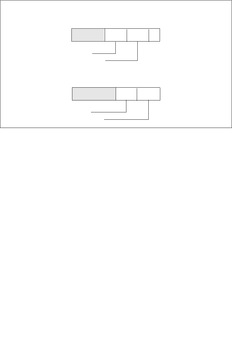
Vol. 3A 7-23
MULTIPLE-PROCESSOR MANAGEMENT
For P6 family processors, the APIC ID that is assigned to a processor during power-up and
initialization is 4 bits (see Figure 7-2). Here, bits 0 and 1 form a 2-bit processor (or socket) iden-
tifier and bits 2 and 3 form a 2-bit cluster ID.
7.6 HYPER-THREADING AND MULTI-CORE TECHNOLOGY
Hyper-Threading Technology and multi-core technology are extensions to IA-32 architecture
that enable a single physical processor to execute two or more separate code streams (called
threads) concurrently. In Hyper-Threading Technology, a single processor core provides two
logical processors that share execution resources (see Section 7.8, “Intel® Hyper-Threading
Technology Architecture”). In multi-core technology, a physical processor package provides
two or more processor cores. Both configurations require chipsets and a BIOS that support the
technologies.
Software should not rely on IA-32 processor names to determine whether a processor supports
Hyper-Threading Technology or multi-core technology. Use the CPUID instruction to deter-
mine processor capability (see Section 7.7.2, “Initializing Dual-Core IA-32 Processors”).
Figure 7-2. Interpretation of APIC ID in Early MP Systems
0
Processor ID
17 432
Cluster
Reserved
0
Processor ID
17 4325
Cluster
Reserved
APIC ID Format for Intel Xeon Processors that
APIC ID Format for P6 Family Processors
0
do not Support Hyper-Threading Technology

7-24 Vol. 3A
MULTIPLE-PROCESSOR MANAGEMENT
7.7 DETECTING HARDWARE MULTI-THREADING SUPPORT
AND TOPOLOGY
Use the CPUID instruction to detect the presence of hardware multi-threading support in a phys-
ical processor. The following can be interpreted:
•Hardware Multi-Threading feature flag (CPUID.1:EDX[28] = 1) — Indicates when set
that the physical package is capable of supporting Hyper-Threading Technology and/or
multiple cores.
•Logical processors per Package (CPUID.1:EBX[23:16]) — Indicates the maximum
number of logical processors in a physical package. This represents the hardware
capability as the processor has been manufactured.2
•Cores per Package3 (CPUID.4:EAX[31:26] + 1) — The maximum number of cores in a
physical package is indicated by one plus the decimal value represented in
CPUID.4:EAX[31:26].
The CPUID feature flag may indicate support for hardware multi-threading when only one
logical processor available in the package. In this case, the decimal value represented by bits 16
through 23 in the EBX register will have a value of 1.
Software should note that the number of logical processors enabled by system software may be
less than the value of “logical processors per package”. Similarly, the number of cores enabled
by system software may be less than the value of “cores per package”.
7.7.1 Initializing IA-32 Processors
Supporting Hyper-Threading Technology
The initialization process for an MP system that contains IA-32 processors that support Hyper-
Threading Technology is the same as for conventional MP systems (see Section 7.5, “Multiple-
Processor (MP) Initialization”). One logical processor in the system is selected as the BSP and
other processors (or logical processors) are designated as APs. The initialization process is iden-
tical to that described in Section 7.5.3, “MP Initialization Protocol Algorithm for
Intel Xeon Processors,” and Section 7.5.4, “MP Initialization Example.”
During initialization, each logical processor is assigned an APIC ID that is stored in the local
APIC ID register for each logical processor. If two or more processors supporting Hyper-
Threading Technology are present, each logical processor on the system bus is assigned a unique
ID (see Section 7.10.2, “Identifying Logical Processors in an MP System”). Once logical
processors have APIC IDs, software communicates with them by sending APIC IPI messages.
2. Operating system and BIOS may implement features that reduce the number of logical processors avail-
able in a platform to applications at runtime to less than the number of physical packages times the num-
ber of hardware-capable logical processors per package.
3. Software must check CPUID for its support of leaf 4 when implementing support for multi-core. If CPUID
leaf 4 is not available at runtime, software should handle the situation as if there is only one core per pack-
age.

Vol. 3A 7-25
MULTIPLE-PROCESSOR MANAGEMENT
7.7.2 Initializing Dual-Core IA-32 Processors
The initialization process for an MP system that contains dual-core IA-32 processors is the same
as for conventional MP systems (see Section 7.5, “Multiple-Processor (MP) Initialization”). A
logical processor in one core is selected as the BSP; other logical processors are designated as
APs.
During initialization, each logical processor is assigned an APIC ID. Once logical processors
have APIC IDs, software may communicate with them by sending APIC IPI messages.
7.7.3 Executing Multiple Threads on an IA-32 Processor
Supporting Hardware Multi-Threading
Upon completing the operating system boot-up procedure, the bootstrap processor (BSP)
executes operating system code. Other logical processors are placed in the halt state. To execute
a code stream (thread) on a halted logical processor, the operating system issues an interpro-
cessor interrupt (IPI) addressed to the halted logical processor. In response to the IPI, the
processor wakes up and begins executing the thread identified by the interrupt vector received
as part of the IPI.
To manage execution of multiple threads on logical processors, an operating system can use
conventional symmetric multiprocessing (SMP) techniques. For example, the operating-system
can use a time-slice or load balancing mechanism to periodically interrupt each of the active
logical processors. Upon interrupting a logical processor, the operating system checks its run
queue for a thread waiting to be executed and dispatches the thread to the interrupted logical
processor.
7.7.4 Handling Interrupts on an IA-32 Processor
Supporting Hardware Multi-Threading
Interrupts are handled on IA-32 processors supporting Hyper-Threading Technology as they
are on conventional MP systems. External interrupts are received by the I/O APIC, which
distributes them as interrupt messages to specific logical processors (see Figure 7-3).
Logical processors can also send IPIs to other logical processors by writing to the ICR register
of its local APIC (see Section 8.6, “Issuing Interprocessor Interrupts”). This also applies to dual-
core IA-32 processors.
7-26 Vol. 3A
MULTIPLE-PROCESSOR MANAGEMENT
7.8 INTEL® HYPER-THREADING TECHNOLOGY
ARCHITECTURE
Figure 7-4 shows a generalized view of an IA-32 processor supporting Hyper-Threading Tech-
nology, using the Intel Xeon processor MP as an example. This implementation of the Hyper-
Threading Technology consists of two logical processors (each represented by a separate IA-32
architectural state) which share the processor’s execution engine and the bus interface. Each
logical processor also has its own advanced programmable interrupt controller (APIC).
Figure 7-3. Local APICs and I/O APIC in MP System Supporting HT Technology
I/O APIC External
Interrupts
System Chip Set
Bridge
PCI
Interrupt Messages
Local APIC
Logical
Processor 0
Local APIC
Logical
Processor 1
Hyper-Threading Technology
IA-32 Processor with
Bus Interface
Processor Core
IPIs Interrupt
Messages
Local APIC
Logical
Processor 0
Local APIC
Logical
Processor 1
Hyper-Threading Technology
IA-32 Processor with
Bus Interface
Processor Core
IPIs Interrupt
Messages
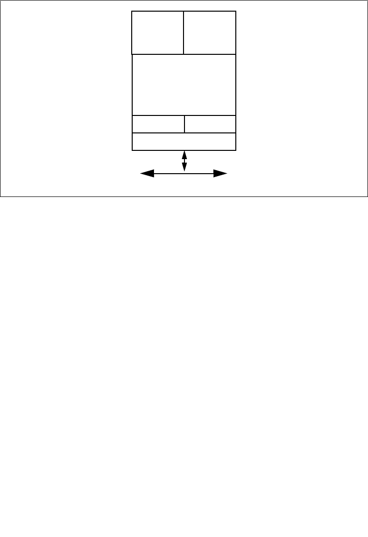
Vol. 3A 7-27
MULTIPLE-PROCESSOR MANAGEMENT
7.8.1 State of the Logical Processors
The following features are part of the architectural state of logical processors within IA-32
processors supporting Hyper-Threading Technology. The features can be subdivided into three
groups:
•Duplicated for each logical processor
•Shared by logical processors in a physical processor
•Shared or duplicated, depending on the implementation
The following features are duplicated for each logical processor:
•General purpose registers (EAX, EBX, ECX, EDX, ESI, EDI, ESP, and EBP)
•Segment registers (CS, DS, SS, ES, FS, and GS)
•EFLAGS and EIP registers. Note that the CS and EIP registers for each logical processor
point to the instruction stream for the thread being executed by the logical processor.
•x87 FPU registers (ST0 through ST7, status word, control word, tag word, data operand
pointer, and instruction pointer)
•MMX registers (MM0 through MM7)
•XMM registers (XMM0 through XMM7) and the MXCSR register
•Control registers (CR0, CR2, CR3, CR4) and system table pointer registers (GDTR,
LDTR, IDTR, task register)
Figure 7-4. IA-32 Processor with Two Logical Processors Supporting HT Technology
Logical
Processor 0
Architectural
State
Bus Interface
Local APIC
Local APIC
Logical
Processor 1
Architectural
State
Execution Engine
System Bus

7-28 Vol. 3A
MULTIPLE-PROCESSOR MANAGEMENT
•Debug registers (DR0, DR1, DR2, DR3, DR6, DR7) and the debug control MSRs
•Machine check global status (IA32_MCG_STATUS) and machine check capability
(IA32_MCG_CAP) MSRs
•Thermal clock modulation and ACPI Power management control MSRs
•Time stamp counter MSRs
•Most of the other MSR registers, including the page attribute table (PAT). See the
exceptions below.
•Local APIC registers.
•Additional general purpose registers (R8-R15), XMM registers (XMM8-XMM15), control
register, IA32_EFER on processors that support Intel EM64T.
The following features are shared by logical processors:
•IA32_MISC_ENABLE MSR (MSR address 1A0H)
•Memory type range registers (MTRRs)
Whether the following features are shared or duplicated is implementation-specific:
•Machine check architecture (MCA) MSRs (except for the IA32_MCG_STATUS and
IA32_MCG_CAP MSRs)
•Performance monitoring control and counter MSRs
7.8.2 APIC Functionality
When a processor supporting Hyper-Threading Technology support is initialized, each logical
processor is assigned a local APIC ID (see Table 8-1). The local APIC ID serves as an ID for
the logical processor and is stored in the logical processor’s APIC ID register. If two or more
IA-32 processors supporting Hyper-Threading Technology are present in a dual processor (DP)
or MP system, each logical processor on the system bus is assigned a unique local APIC ID (see
Section 7.10.2, “Identifying Logical Processors in an MP System”).
Software communicates with local processors using the APIC’s interprocessor interrupt (IPI)
messaging facility. Setup and programming for APICs is identical in processors that support and
do not support Intel Hyper-Threading Technology. See Chapter 8, “Advanced Programmable
Interrupt Controller (APIC),” for a detailed discussion.
7.8.3 Memory Type Range Registers (MTRR)
MTRRs in a processor supporting Hyper-Threading Technology are shared by logical proces-
sors. When one logical processor updates the setting of the MTRRs, settings are automatically
shared with the other logical processors in the same physical package.
IA-32 architecture requires that all MP systems based on IA-32 processors (this includes logical
processors) MUST use an identical MTRR memory map. This gives software a consistent view

Vol. 3A 7-29
MULTIPLE-PROCESSOR MANAGEMENT
of memory, independent of the processor on which it is running. See Section 10.11, “Memory
Type Range Registers (MTRRs),” for information on setting up MTRRs.
7.8.4 Page Attribute Table (PAT)
Each logical processor has its own PAT MSR (IA32_CR_PAT). However, as described in
Section 10.12, “Page Attribute Table (PAT),” the PAT MSR settings must be the same for all
processors in a system, including the logical processors.
7.8.5 Machine Check Architecture
In the HT Technology context, all of the machine check architecture (MCA) MSRs (except for
the IA32_MCG_STATUS and IA32_MCG_CAP MSRs) are duplicated for each logical
processor. This permits logical processors to initialize, configure, query, and handle machine-
check exceptions simultaneously within the same physical processor. The design is compatible
with machine check exception handlers that follow the guidelines given in Chapter 14,
“Machine-Check Architecture.”
The IA32_MCG_STATUS MSR is duplicated for each logical processor so that its machine
check in progress bit field (MCIP) can be used to detect recursion on the part of MCA handlers.
In addition, the MSR allows each logical processor to determine that a machine-check exception
is in progress independent of the actions of another logical processor in the same physical
package.
Because the logical processors within a physical package are tightly coupled with respect to
shared hardware resources, both logical processors are notified of machine check errors that
occur within a given physical processor. If machine-check exceptions are enabled when a fatal
error is reported, all the logical processors within a physical package are dispatched to the
machine-check exception handler. If machine-check exceptions are disabled, the logical proces-
sors enter the shutdown state and assert the IERR# signal.
When enabling machine-check exceptions, the MCE flag in control register CR4 should be set
for each logical processor.
7.8.6 Debug Registers and Extensions
Each logical processor has its own set of debug registers (DR0, DR1, DR2, DR3, DR6, DR7)
and its own debug control MSR. These can be set to control and record debug information for
each logical processor independently. Each logical processor also has its own last branch records
(LBR) stack.
7.8.7 Performance Monitoring Counters
Performance counters and their companion control MSRs are shared between the logical proces-
sors within the physical processor. As a result, software must manage the use of these resources.

7-30 Vol. 3A
MULTIPLE-PROCESSOR MANAGEMENT
The performance counter interrupts, events, and precise event monitoring support can be set up
and allocated on a per thread (per logical processor) basis.
See Section 18.14, “Performance Monitoring and Hyper-Threading Technology,” for a discus-
sion of performance monitoring in the Intel Xeon processor MP.
7.8.8 IA32_MISC_ENABLE MSR
The IA32_MISC_ENABLE MSR (MSR address 1A0H) is shared between the logical proces-
sors in an IA-32 processor supporting Hyper-Threading Technology. Thus the architectural
features that this register controls are set the same for all the logical processors in the same phys-
ical package.
7.8.9 Memory Ordering
The logical processors in an IA-32 processor supporting Hyper-Threading Technology obey the
same rules for memory ordering as IA-32 processors without HT Technology (see Section 7.2,
“Memory Ordering”). Each logical processor uses a processor-ordered memory model that can
be further defined as “write-ordered with store buffer forwarding.” All mechanisms for strength-
ening or weakening the memory ordering model to handle special programming situations apply
to each logical processor.
7.8.10 Serializing Instructions
As a general rule, when a logical processor in an IA-32 processor supporting Hyper-Threading
Technology executes a serializing instruction, only that logical processor is affected by the oper-
ation. An exception to this rule is the execution of the WBINVD, INVD, and WRMSR instruc-
tions; and the MOV CR instruction when the state of the CD flag in control register CR0 is
modified. Here, both logical processors are serialized.
7.8.11 MICROCODE UPDATE Resources
In an IA-32 processor supporting Hyper-Threading Technology, the microcode update facilities
are shared between the logical processors; either logical processor can initiate an update. Each
logical processor has its own BIOS signature MSR (IA32_BIOS_SIGN_ID at MSR address
8BH). When a logical processor performs an update for the physical processor, the
IA32_BIOS_SIGN_ID MSRs for resident logical processors are updated with identical infor-
mation. If logical processors initiate an update simultaneously, the processor core provides the
necessary synchronization needed to insure that only one update is performed at a time.
Operating system microcode update drivers that adhere to Intel’s guidelines do not need to be
modified to run on an IA-32 processor supporting Hyper-Threading Technology.

Vol. 3A 7-31
MULTIPLE-PROCESSOR MANAGEMENT
7.8.12 Self Modifying Code
IA-32 processors supporting Hyper-Threading Technology support self-modifying code, where
data writes modify instructions cached or currently in flight. They also support cross-modifying
code, where on an MP system writes generated by one processor modify instructions cached or
currently in flight on another. See Section 7.1.3, “Handling Self- and Cross-Modifying Code,”
for a description of the requirements for self- and cross-modifying code in an IA-32 processor.
7.8.13 Implementation-Specific HT Technology Facilities
The following non-architectural facilities are implementation-specific in IA-32 processors
supporting Hyper-Threading Technology:
•Caches
•Translation lookaside buffers (TLBs)
•Thermal monitoring facilities
The Intel Xeon processor MP implementation is described in the following sections.
7.8.13.1 Processor Caches
For the Intel Xeon processor MP, the caches are shared. Any cache manipulation instruction that
is executed on one logical processor has a global effect on the cache hierarchy of the physical
processor. Note the following:
•WBINVD instruction — The entire cache hierarchy is invalidated after modified data is
written back to memory. All logical processors are stopped from executing until after the
write-back and invalidate operation is completed. A special bus cycle is sent to all caching
agents.
•INVD instruction — The entire cache hierarchy is invalidated without writing back
modified data to memory. All logical processors are stopped from executing until after the
invalidate operation is completed. A special bus cycle is sent to all caching agents.
•CLFLUSH instruction — The specified cache line is invalidated from the cache
hierarchy after any modified data is written back to memory and a bus cycle is sent to all
caching agents, regardless of which logical processor caused the cache line to be filled.
•CD flag in control register CR0 — Each logical processor has its own CR0 control
register, and thus its own CD flag in CR0. The CD flags for the two logical processors are
ORed together, such that when any logical processor sets its CD flag, the entire cache is
nominally disabled.
7.8.13.2 Processor Translation Lookaside Buffers (TLBs)
In an Intel Xeon processor MP, data cache TLBs are shared. The instruction cache TLB is dupli-
cated in each logical processor.

7-32 Vol. 3A
MULTIPLE-PROCESSOR MANAGEMENT
Entries in the TLBs are tagged with an ID that indicates the logical processor that initiated the
translation. This tag applies even for translations that are marked global using the page global
feature for memory paging.
When a logical processor performs a TLB invalidation operation, only the TLB entries that are
tagged for that logical processor are flushed. This protocol applies to all TLB invalidation oper-
ations, including writes to control registers CR3 and CR4 and uses of the INVLPG instruction.
7.8.13.3 Thermal Monitor
In an Intel Xeon processor MP, logical processors share the catastrophic shutdown detector and
the automatic thermal monitoring mechanism (see Section 13.4, “Thermal Monitoring and
Protection”). Sharing results in the following behavior:
•If the processor’s core temperature rises above the preset catastrophic shutdown temper-
ature, the processor core halts execution, which causes both logical processors to stop
execution.
•When the processor’s core temperature rises above the preset automatic thermal monitor
trip temperature, the clock speed of the processor core is automatically modulated, which
effects the execution speed of both logical processors.
For software controlled clock modulation, each logical processor has its own
IA32_CLOCK_MODULATION MSR, allowing clock modulation to be enabled or disabled on
a logical processor basis. Typically, if software controlled clock modulation is going to be used,
the feature must be enabled for all the logical processors within a physical processor and the
modulation duty cycle must be set to the same value for each logical processor. If the duty cycle
values differ between the logical processors, the processor clock will be modulated at the highest
duty cycle selected.
7.8.13.4 External Signal Compatibility
This section describes the constraints on external signals received through the pins of an Intel
Xeon processor MP and how these signals are shared between its logical processors.
•STPCLK# — A single STPCLK# pin is provided on the physical package of the Intel
Xeon processor MP. External control logic uses this pin for power management within the
system. When the STPCLK# signal is asserted, the processor core transitions to the stop-
grant state, where instruction execution is halted but the processor core continues to
respond to snoop transactions. Regardless of whether the logical processors are active or
halted when the STPCLK# signal is asserted, execution is stopped on both logical
processors and neither will respond to interrupts.
In MP systems, the STPCLK# pins on all physical processors are generally tied together.
As a result this signal affects all the logical processors within the system simultaneously.
•LINT0 and LINT1 pins — An Intel Xeon processor MP has only one set of LINT0 and
LINT1 pins, which are shared between the logical processors. When one of these pins is
asserted, both logical processors respond unless the pin has been masked in the APIC local

Vol. 3A 7-33
MULTIPLE-PROCESSOR MANAGEMENT
vector tables for one or both of the logical processors.
Typically in MP systems, the LINT0 and LINT1 pins are not used to deliver interrupts to
the logical processors. Instead all interrupts are delivered to the local processors through
the I/O APIC.
•A20M# pin — On an IA-32 processor, the A20M# pin is typically provided for compati-
bility with the Intel 286 processor. Asserting this pin causes bit 20 of the physical address
to be masked (forced to zero) for all external bus memory accesses. The Intel Xeon
processor MP provides one A20M# pin, which affects the operation of both logical
processors within the physical processor. This configuration is compatible with the IA-32
architecture.
7.9 DUAL-CORE ARCHITECTURE
This section describes the architecture of dual-core IA-32 processors. The discussion is appli-
cable to the Intel Pentium processor Extreme Edition and Pentium D and Dual-core Intel Xeon
processor. Features vary across different microarchitectures and are detectable using CPUID.
In general, each processor core has dedicated microarchitectural resources identical to a single-
processor implementation of the underlying microarchitecture without hardware multi-
threading capability. Each logical processor in a dual-core IA-32 processor (whether supporting
Hyper-Threading Technology or not) has its own APIC functionality, PAT, machine check archi-
tecture, debug registers and extensions. Each logical processor handles serialization instructions
or self-modifying code on its own. Memory order is handled the same way as in Hyper-
Threading Technology.
The topology of the cache hierarchy (with respect to whether a given cache level is shared by
one or more processor cores or by all logical processors in the physical package) depends on the
processor implementation. Software must use the deterministic cache parameter leaf of CPUID
instruction to discover the cache-sharing topology between the logical processors in a multi-
threading environment.
7.9.1 Logical Processor Support
The topological composition of processor cores and logical processors in a multi-core IA-32
architecture processor can be discovered using CPUID. Within each processor core, one or more
logical processors may be available.
System software must follow the requirement MP initialization sequences (see Section 7.5,
“Multiple-Processor (MP) Initialization”) to recognize and enable logical processors. At
runtime, software can enumerate those logical processors enabled by system software to identify
the topological relationships between these logical processors. (See Section 7.10.4, “Identifying
Topological Relationships in a MP System”).

7-34 Vol. 3A
MULTIPLE-PROCESSOR MANAGEMENT
7.9.2 Memory Type Range Registers (MTRR)
MTRR is shared between two logical processors sharing a processor core if the physical
processor supports Hyper-Threading Technology. MTRR is not shared between logical proces-
sors located in different cores or different physical packages.
IA-32 architecture requires that all MP systems based on IA-32 processors (this includes logical
processors) use an identical MTRR memory map. This gives software a consistent view of
memory, independent of the processor on which it is running.
See Section 10.11, “Memory Type Range Registers (MTRRs).”
7.9.3 Performance Monitoring Counters
Performance counters and their companion control MSRs are shared between two logical
processors sharing a processor core if the physical package supports Hyper-Threading Tech-
nology. They are not shared between logical processors in different cores or different physical
packages. As a result, software must manage the use of these resources, based on the topology
of performance monitoring resources. Performance counter interrupts, events, and precise event
monitoring support can be set up and allocated on a per thread (per logical processor) basis.
See Section 18.14, “Performance Monitoring and Hyper-Threading Technology.”
7.9.4 IA32_MISC_ENABLE MSR
The IA32_MISC_ENABLE MSR (MSR address 1A0H) is shared between two logical proces-
sors sharing a processor core if the physical package supports Hyper-Threading Technology.
The MSR is not shared between logical processors in different cores or different physical pack-
ages. This means that the architectural features that this register controls are set the same for the
logical processors in the same core.
7.9.5 MICROCODE UPDATE Resources
Microcode update facilities are shared between two logical processors sharing a processor core
if the physical package supports Hyper-Threading Technology. They are not shared between
logical processors in different cores or different physical packages. Either logical processor that
has access to the microcode update facility can initiate an update.
Each logical processor has its own BIOS signature MSR (IA32_BIOS_SIGN_ID at MSR
address 8BH). When a logical processor performs an update for the physical processor, the
IA32_BIOS_SIGN_ID MSRs for resident logical processors are updated with identical infor-
mation. If logical processors initiate an update simultaneously, the processor core provides the
synchronization needed to ensure that only one update is performed at a time.

Vol. 3A 7-35
MULTIPLE-PROCESSOR MANAGEMENT
7.10 PROGRAMMING CONSIDERATIONS FOR HARDWARE
MULTI-THREADING CAPABLE PROCESSORS
In a multi-threading environment, there may be certain hardware resources that are physically
shared at some level of the hardware topology. In the multi-processor systems, typically bus and
memory sub-systems are physically shared between multiple sockets. Within a hardware multi-
threading capable processors, certain resources are provided for each processor core, while other
resources may be provided for each logical processors (see Section 7.8, “Intel® Hyper-
Threading Technology Architecture,” and Section 7.9, “Dual-Core Architecture”).
From a software programming perspective, control transfer of processor operation is managed
at the granularity of logical processor (operating systems dispatch a runnable task by allocating
an available logical processor on the platform). To manage the topology of shared resources in
a multi-threading environment, it is useful for software to understand and manage resources that
may be shared by more than one logical processors. This can be facilitated by mapping several
levels of hierarchical labels to the initial APIC_ID of each logical processor to identify the
topology of shared resources.
7.10.1 Hierarchical Mapping of Shared Resources
The initial APIC_ID value associated with each logical processor in a multi-processor system is
unique (see Section 7.7, “Detecting Hardware Multi-Threading Support and Topology”). This
8-bit value can be decomposed into sub-fields, where each sub-field corresponds a hierarchical
level of the topological mapping of hardware resources.
The decomposition of an initial APIC_ID may consist of 4 sub fields, matching 4 levels of hier-
archy:
•Cluster — Some multi-threading environments consists of multiple clusters of multi-
processor systems. The CLUSTER_ID sub-field distinguishes different clusters. For non-
clustered systems, CLUSTER_ID is usually 0.
•Package — A multi-processor system consists of two or more sockets, each mates with a
physical processor package. The PACKAGE_ID sub-field distinguishes different physical
packages within a cluster.
•Core — A physical processor package consists of one or more processor cores. The
CORE_ID sub-field distinguishes processor cores in a package. For a single-core
processor, the width of this bit field is 0.
•SMT — A processor core provides one or more logical processors sharing execution
resources. The SMT_ID sub-field distinguishes logical processors in a core. The width of
this bit field is non-zero if a processor core provides more than one logical processors.
SMT and CORE sub-fields are bit-wise contiguous in the 8-bit APIC_ID field (see Figure 7-5).
The width of each sub-field depends on hardware and software configurations. Field widths can
be determined at runtime using the algorithm discussed below (Example 7-1 through Example
7-3). Figure 7-6 depicts the relationships of three of the hierarchical sub-fields in a hypothetical
MP system.
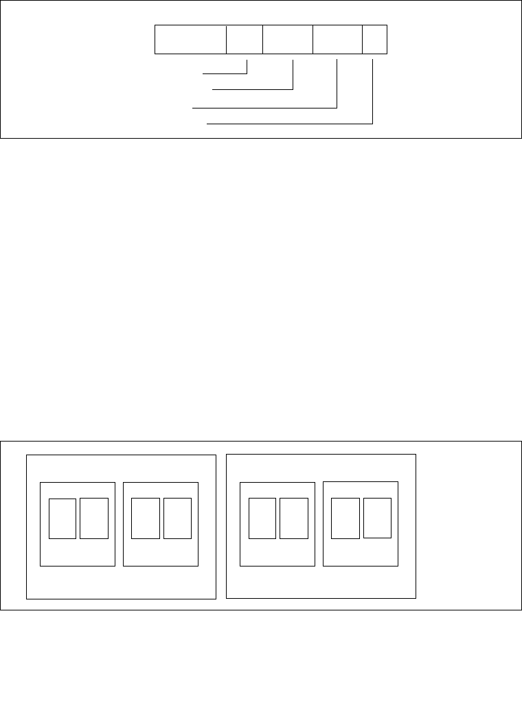
7-36 Vol. 3A
MULTIPLE-PROCESSOR MANAGEMENT
The value of valid APIC_IDs need not be contiguous across package boundary or core bound-
aries.
7.10.2 Identifying Logical Processors in an MP System
For any IA-32 processor, system hardware establishes an initial APIC ID that is unique for each
logical processor following power-up or RESET (see Section 7.7.1). Each logical processor on
the system is allocated an initial APIC ID. BIOS may implement features that tell the OS to
support less than the total number of logical processors on the system bus. Those logical proces-
sors that are not available to applications at runtime are halted during the OS boot process. As a
result, the number valid local APIC_IDs that can be queried by affinitizing-current-thread-
context (See Example 7-3) is limited to the number of logical processors enabled at runtime by
the OS boot process.
Table 7-1 shows the APIC IDs that are initially reported for logical processors in a system with
four MP-type Intel Xeon processors (a total of 8 logical processors, each physical package has
one processor core and supports Hyper-Threading Technology). Of the two logical processors
within a Intel Xeon processor MP, logical processor 0 is designated the primary logical
processor and logical processor 1 as the secondary logical processor.
Figure 7-5. Generalized Four level Interpretation of the initial APIC ID
Figure 7-6. Topological Relationships between Hierarchical IDs in a Hypothetical MP
Platform
0
Package ID
SMT ID
7
Cluster ID
Reserved
Core ID
Package 0
Core 0
T0 T1
Core1
T0 T1
Package 1
Core 0
T0 T1
Core1
T0 T1 SMT_ID
Core ID
Package ID

Vol. 3A 7-37
MULTIPLE-PROCESSOR MANAGEMENT
Table 7-2 shows the initial APIC IDs for a hypothetical situation with a dual processor system.
Each physical package providing two processor cores, and each processor core also supporting
Hyper-Threading Technology.
Table 7-1. Initial APIC IDs for the Logical Processors in a System that has Four MP-Type
Intel Xeon Processors Supporting Hyper-Threading Technology 1
Initial APIC ID of Logical
Processor Package ID Core ID SMT ID
0H 0H 0H 0H
1H 0H 0H 1H
2H 1H 0H 0H
3H 1H 0H 1H
4H 2H 0H 0H
5H 2H 0H 1H
6H 3H 0H 0H
7H 3H 0H 1H
NOTE:
1. Because information on the number of processor cores in a physical package was not available in early
single-core processors supporting Hyper-Threading Technology, the core ID can be treated as 0.
Table 7-2. Initial APIC IDs for the Logical Processors in a System that has Two Physical
Processors Supporting Dual-Core and Hyper-Threading Technology
Initial APIC ID of a Logical
Processor Package ID Core ID SMT ID
0H 0H 0H 0H
1H 0H 0H 1H
2H 0H 1H 0H
3H 0H 1H 1H
4H 1H 0H 0H
5H 1H 0H 1H
6H 1H 1H 0H
7H 1H 1H 1H

7-38 Vol. 3A
MULTIPLE-PROCESSOR MANAGEMENT
7.10.3 Algorithm for Three-Level Mappings of APIC_ID
Software can gather the initial APIC_IDs for each logical processor supported by the operating
system at runtime4 and extract identifiers corresponding to the three levels of sharing topology
(package, core, and SMT). The algorithms below focus on a non-clustered MP system for
simplicity. They do not assume initial APIC_IDs are contiguous or that all logical processors on
the platform are enabled.
Intel supports multi-threading systems where all physical processors report identical values in
CPUID.1:EBX[23:16]), CPUID.4:EAX[31:26], and CPUID.4:EAX[25:14]. The algorithms
below assume the target system has symmetry across physical package boundaries with respect
to the number of logical processors per package, number of cores per package, and cache
topology within a package.
The extraction algorithm (for three-level mappings of an initial APIC_ID) uses the following
support routines (Example 7-1):
1. Detect capability for hardware multi-threading support in the processor.
2. Identify the maximum number of logical processors in a physical processor package. This
is used to determine the topological relationship between logical processors and the
physical package.
3. Identify the maximum number of processor cores in a physical processor package. This is
used to determine the topological relationship between processor cores and the physical
package.
4. Extract the initial APIC ID for the logical processor where the current thread is executing.
5. Calculate a mask from the maximum count that the bit field can represent.
6. Use full 8-bit ID and mask to extract sub-field IDs.
Example 7-1 Support Routines for Detecting Hardware Multi-Threading and
Identifying the Relationships Between Package, Core and Logical
Processors
1. Detect support for Hardware Multi-Threading Support in a processor.
// Returns a non-zero value if CPUID reports the presence of hardware multi-threading
// support in the physical package where the current logical processor is located.
// This does not guarrantee BIOS or OS will enable all logical processors in the physical
// package and make them available to applications.
// Returns zero if hardware multi-threading is not present.
#define HWMT_BIT 0x10000000
4. As noted in Section 7.7 and Section 7.10.2, the number of logical processors supported by the OS at
runtime may be less than the total number logical processors available in the platform hardware.

Vol. 3A 7-39
MULTIPLE-PROCESSOR MANAGEMENT
unsigned int HWMTSupported(void)
{try { // verify cpuid instruction is supported
execute cpuid with eax = 0 to get vendor string
execute cpuid with eax = 1 to get feature flag and signature
}
except (EXCEPTION_EXECUTE_HANDLER) {
return 0 ; // CPUID is not supported; So HW Multi-threading capability is not present
}
// Check to see if this a Genuine Intel Processor
if (vendor string EQ GenuineIntel) {
return (feature_flag_edx & HWMT_BIT); // bit 28
}
return 0;
}
2. Find the Max number of logical processors per physical processor package.
#define NUM_LOGICAL_BITS 0x00FF0000
// EBX[23:16] indicates the max number of logical processors per package.
// Returns the max number of logical processors per physical processor package;
// the actual number of logical processors per package enabled by OS may be less.
// Software should not assume the value of (cpuid.1.ebx[23:16]) must be power of 2.
unsigned char MaxLPPerPackage(void)
{if (!HWMTSupported()) return 1;
execute cpuid with eax = 1
store returned value of ebx
return (unsigned char) ((reg_ebx & NUM_LOGICAL_BITS) >> 16);
}
3. Find the max number of processor cores per physical processor package.
// Returns the max number of processor cores per physical processor package;
// the actual number of processor cores per package that are enabled may be less.
// Software should not assume the value of (cpuid.4.eax[31:26] +1) must be power of 2.
unsigned MaxCoresPerPackage(void)
{if (!HWMTSupported()) return (unsigned char) 1;
if cpuid supports leaf number 4
{ // we can retrieve multi-core topology info using leaf 4
execute cpuid with eax = 4, ecx = 0

7-40 Vol. 3A
MULTIPLE-PROCESSOR MANAGEMENT
store returned value of eax
return (unsigned ) ((reg_eax >> 26) +1);
}
else // must be a single-core processor
return 1;
}
4. Extract the initial APIC ID of a logical processor.
#define INITIAL_APIC_ID_BITS 0xFF000000 // EBX[31:24] initial APIC ID
// Returns the 8-bit unique initial APIC ID for the processor ruuning the code.
// Software can use OS services to affinitize the current thread to each logical processor
// available under the OS to gather the initial APIC_IDs for each logical processor.
unsigned char GetInitAPIC_ID (void)
{unsigned int reg_ebx = 0;
execute cpuid with eax = 1
store returned value of ebx
return (unsigned char) ((reg_ebx & INITIAL_APIC_ID_BITS) >> 24;
}
5. Find the width of a bit-field mask from the maximum count of the bit-field.
// Returns the mask bit width of a bit field from the maximum count that bit field can represent.
// This algorithm does not assume ‘Max_Count’ to have a value equal to power of 2.
unsigned FindMaskWidth(Unsigned Max_Count)
{unsigned int mask_width, cnt = Max_Count;
__asm { mov eax, cnt
mov ecx, 0
mov mask_width, ecx
dec eax
bsr cx, ax
jz next
inc cx
mov mask_width, ecx
next:
mov eax, mask_width
}
return mask_width;
}

Vol. 3A 7-41
MULTIPLE-PROCESSOR MANAGEMENT
6. Extract a sub ID given a full ID, maximum sub ID value and shift count.
// Returns the value of the sub ID, this is not a zero-based value
Unsigned char GetSubID(unsigned char Full_ID, unsigned char MaxSubIDvalue, unsigned
char Shift_Count)
{MaskWidth = FindMaskWidth(MaxSubIDValue);
MaskBits = ((uchar) (0xff << Shift_Count)) ^ ((uchar) (0xff << Shift_Count + MaskWidth)) ;
SubID = Full_ID & MaskBits;
Return SubID;
}
Software must not assume local APIC_ID values in an MP system are consecutive. Non-consec-
utive local APIC_IDs may be the result of hardware configurations or debug features imple-
mented in the BIOS or OS.
An identifier for each hierarchical level can be extracted from an 8-bit APIC_ID using the
support routines illustrated in Example 7-1. The appropriate bit mask and shift value to construct
the appropriate bit mask for each level must be determined dynamically at runtime.
7.10.4 Identifying Topological Relationships in a MP System
To detect the number of physical packages, processor cores, or other topological relationships
in a MP system, the following procedures are recommended:
•Extract the three-level identifiers from the APIC ID of each logical processor enabled by
system software. The sequence is as follows (See the pseudo code shown in Example 7-2
and support routines shown in Example 7-1):
•The extraction start from the right-most bit field, corresponding to SMT_ID, the
innermost hierarchy in a three-level topology (See Figure 7-6). For the right-most
bit field, the shift value of the working mask is zero. The width of the bit field is
determined dynamically using the maximum number of logical processor per core,
which can be derived from information provided from CPUID.
•To extract the next bit-field, the shift value of the working mask is determined
from the width of the bit mask of the previous step. The width of the bit field is
determined dynamically using the maximum number of cores per package.
•To extract the remaining bit-field, the shift value of the working mask is
determined from the maximum number of logical processor per package. So the
remaining bits in the APIC ID (excluding those bits already extracted in the two
previous steps) are extracted as the third identifier. This applies to a non-clustered
MP system, or if there is no need to distinguish between PACKAGE_ID and
CLUSTER_ID.
If there is need to distinguish between PACKAGE_ID and CLUSTER_ID,
PACKAGE_ID can be extracted using an algorithm similar to the extraction of

7-42 Vol. 3A
MULTIPLE-PROCESSOR MANAGEMENT
CORE_ID, assuming the number of physical packages in each node of a clustered
system is symmetric.
•Assemble the three-level identifiers of SMT_ID, CORE_ID, PACKAGE_IDs into arrays
for each enabled logical processor. This is shown in Example 7-3a.
•To detect the number of physical packages: use PACKAGE_ID to identify those logical
processors that reside in the same physical package. This is shown in Example 7-3b. This
example also depicts a technique to construct a mask to represent the logical processors
that reside in the same package.
•To detect the number of processor cores: use CORE_ID to identify those logical processors
that reside in the same core. This is shown in Example 7-3. This example also depicts a
technique to construct a mask to represent the logical processors that reside in the same
core.
In Example 7-2, the numerical ID value can be obtained from the value extracted with the mask
by shifting it right by shift count. Algorithms below do not shift the value. The assumption is
that the SubID values can be compared for equivalence without the need to shift.
Example 7-2 Pseudo Code Depicting Three-level Extraction Algorithm
For Each local_APIC_ID{
// Determine MaxLPPerCore available in hardware
// This algorithm assumes there is symmetry across core boundary, i.e. each core within a
package has the same number of logical processors
MaxLPPerCore = MaxLPPerPackage()/MaxCoresPerPackage();
// Extract SMT_ID first, this is the innermost of the three levels
// bit mask width is determined from MaxLPPerCore topological info.
// shift size is 0, corresponding to the right-most bit-field
SMT_ID = GetSubID(local_APIC_ID, MaxLPPerCore, 0);
// Extract CORE_ID:
// bit width is determined from maximum number of cores per package possible in hardware
// shift count is determined by maximum logical processors per core in hardware
CORE_ID = GetSubID(InitAPIC_ID, MaxCoresPerPackage(), FindMaskWidth(
MaxLPPerCore) );
// Extract PACKAGE_ID:
// Assume single cluster.
// Shift out the mask width for maximum logical processors per package
PackageIDMask = ((uchar) (0xff << FindMaskWidth(MaxLPPerPackage()));
PACKAGE_ID = InitAPIC_ID & PackageIDMask;
}

Vol. 3A 7-43
MULTIPLE-PROCESSOR MANAGEMENT
Example 7-3 Compute the Number of Packages, Cores, and Processor Relationships
in a MP System
a) Assemble lists of PACKAGE_ID, CORE_ID, and SMT_ID of each enabled logical processors
//The BIOS and/or OS may limit the number of logical processors available to applications
// after system boot. The below algorithm will compute topology for the processors visible
// to the thread that is computing it.
// Extract the 3-levels of IDs on every processor
// SystemAffinity is a bitmask of all the processors started by the OS. Use OS specific APIs to
obtain it.
// ThreadAffinityMask is used to affinitize the topology enumeration thread to each processor
using OS specific APIs.
// Allocate per processor arrays to store the Package_ID, Core_ID and SMT_ID for every
started processor
ThreadAffinityMask = 1;
ProcessorNum = 0;
while (ThreadAffinityMask != 0 && ThreadAffinityMask <= SystemAffinity) {
// Check to make sure we can utilize this processor first.
if (ThreadAffinityMask & SystemAffinity){
Set thread to run on the processor specified in ThreadAffinityMask
Wait if necessary and ensure thread is running on specified processor
InitAPIC_ID = GetInitAPIC_ID();
Extract the Package, Core and SMT ID as explained in three level extraction
algorithm
PackageID[ProcessorNUM] = PACKAGE_ID;
CoreID[ProcessorNum] = CORE_ID;
SmtID[ProcessorNum] = SMT_ID;
ProcessorNum++;
}
ThreadAffinityMask <<= 1;
}
NumStartedLPs = ProcessorNum;
b) Using the list of PACKAGE_ID to count the number of physical packages in a MP system
and construct, for each package, a multi-bit mask corresponging to those logical processors
residing in the same package.
// Compute the number of packages by counting the number of processors
// with unique PACKAGE_IDs in the PackageID array.
// Compute the mask of processors in each package.
PackageIDBucket is an array of unique PACKAGE_ID values. Allocate an array of
NumStartedLPs count of entries in this array.
PackageProcessorMask is a corresponding array of the bit mask of processors belonging to
the same package, these are processors with the same PACKAGE_ID

7-44 Vol. 3A
MULTIPLE-PROCESSOR MANAGEMENT
The algorithm below assumes there is symmetry across package boundary if more than
one socket is populated in an MP system.
// Bucket Package IDs and compute processor mask for every package.
PackageNum = 1;
PackageIDBucket[0] = PackageID[0];
ProcessorMask = 1;
PackageProcessorMask[0] = ProcessorMask;
For (ProcessorNum = 1; ProcessorNum < NumStartedLPs; ProcessorNum++) {
ProcessorMask << = 1;
For (i=0; i < PackageNum; i++) {
// we may be comparing bit-fields of logical processors residing in different
// packages, the code below assume package symmetry
If (PackageID[ProcessorNum] == PackageIDBucket[i]) {
PackageProcessorMask[i] |= ProcessorMask;
Break; // found in existing bucket, skip to next iteration
}
}
if (i ==PackageNum) {
//PACKAGE_ID did not match any bucket, start new bucket
PackageIDBucket[i] = PackageID[ProcessorNum];
PackageProcessorMask[i] = ProcessorMask;
PackageNum++;
}
}
// PackageNum has the number of Packages started in OS
// PackageProcessorMask[] array has the processor set of each package
c) Using the list of CORE_ID to count the number of cores in a MP system and construct, for
each core, a multi-bit mask corresponging to those logical processors residing in the same
core.
Processors in the same core can be determined by bucketing the processors with the same
PACKAGE_ID and CORE_ID. Note that code below can BIT OR the values of PACKGE and
CORE ID because they have not been shifted right.
The algorithm below assumes there is symmetry across package boundary if more than one
socket is populated in an MP system.
//Bucketing PACKAGE and CORE IDs and computing processor mask for every core
CoreNum = 1;
CoreIDBucket[0] = PackageID[0] | CoreID[0];
ProcessorMask = 1;
CoreProcessorMask[0] = ProcessorMask;
For (ProcessorNum = 1; ProcessorNum < NumStartedLPs; ProcessorNum++) {
ProcessorMask << = 1;
For (i=0; i < CoreNum; i++) {
// we may be comparing bit-fields of logical processors residing in different
// packages, the code below assume package symmetry

Vol. 3A 7-45
MULTIPLE-PROCESSOR MANAGEMENT
If ((PackageID[ProcessorNum] | CoreID[ProcessorNum]) == CoreIDBucket[i]) {
CoreProcessorMask[i] |= ProcessorMask;
Break; // found in existing bucket, skip to next iteration
}
}
if (i == CoreNum) {
//Did not match any bucket, start new bucket
CoreIDBucket[i] = PackageID[ProcessorNum] | CoreID[ProcessorNum];
CoreProcessorMask[i] = ProcessorMask;
CoreNum++;
}
}
// CoreNum has the number of cores started in the OS
// CoreProcessorMask[] array has the processor set of each core
Other processor relationships such as processor mask of sibling cores can be computed from set
operations of the PackageProcessorMask[] and CoreProcessorMask[].
The algorithm shown above can be applied to earlier generations of single-core IA-32 proces-
sors that support Hyper-Threading Technology and in the situation that the deterministic cache
parameter leaf is not supported. This is handled by ensuring MaxCoresPerPackage() return 1 in
those situations.
7.11 MANAGEMENT OF IDLE AND BLOCKED CONDITIONS
During execution of an IA-32 processor supporting Hyper-Threading Technology with each
logical processor actively executing a thread, logical processors use shared processor resources
(cache lines, TLB entries, and bus accesses) on an as-needed basis. When one logical processor
is idle (no work to do) or blocked (on a lock or semaphore), additional management of the core
execution engine resource can be accomplished by using the HLT (halt), PAUSE, or the
MONITOR/MWAIT instructions.
7.11.1 HLT Instruction
The HLT instruction stops the execution of the logical processor on which it is executed and
places it in a halted state until further notice (see the description of the HLT instruction in
Chapter 3, “Instruction Set Reference, A-M,” of the IA-32 Intel® Architecture Software Devel-
oper’s Manual, Volume 2A). When a logical processor is halted, active logical processors
continue to have full access to the shared resources within the physical package. Here shared
resources that were being used by the halted logical processor become available to active logical
processors, allowing them to execute at greater efficiency. When the halted logical processor
resumes execution, shared resources are again shared among all active logical processors. (See
Section 7.11.6.3, “Halt Idle Logical Processors,” for more information about using the HLT
instruction with IA-32 processors supporting Hyper-Threading Technology.)

7-46 Vol. 3A
MULTIPLE-PROCESSOR MANAGEMENT
7.11.2 PAUSE Instruction
The PAUSE instruction improves the performance of IA-32 processors supporting Hyper-
Threading Technology when executing “spin-wait loops” and other routines where one thread
is accessing a shared lock or semaphore in a tight polling loop. When executing a spin-wait loop,
the processor can suffer a severe performance penalty when exiting the loop because it detects
a possible memory order violation and flushes the core processor’s pipeline. The PAUSE
instruction provides a hint to the processor that the code sequence is a spin-wait loop. The
processor uses this hint to avoid the memory order violation and prevent the pipeline flush. In
addition, the PAUSE instruction de-pipelines the spin-wait loop to prevent it from consuming
execution resources excessively. (See Section 7.11.6.1, “Use the PAUSE Instruction in Spin-
Wait Loops,” for more information about using the PAUSE instruction with IA-32 processors
supporting Hyper-Threading Technology.)
7.11.3 Detecting Support MONITOR/MWAIT Instruction
Streaming SIMD Extensions 3 introduced two instructions (MONITOR and MWAIT) to help
multithreaded software improve thread synchronization. In the initial implementation,
MONITOR and MWAIT are available to software at ring 0. The instructions are conditionally
available at levels greater than 0. Use the following steps to detect the availability of MONITOR
and MWAIT:
•Use CPUID to query the MONITOR bit (CPUID.1.ECX[3] = 1).
•If CPUID indicates support, execute MONITOR inside a TRY/EXCEPT exception handler
and trap for an exception. If an exception occurs, MONITOR and MWAIT are not
supported at a privilege level greater than 0. See Example 7-4.
Example 7-4 Verifying MONITOR/MWAIT Support
boolean MONITOR_MWAIT_works = TRUE;
try {
_asm {
xor ecx, ecx
xor edx, edx
mov eax, MemArea
monitor
}
// Use monitor
} except (UNWIND) {
// if we get here, MONITOR/MWAIT is not supported
MONITOR_MWAIT_works = FALSE;
}

Vol. 3A 7-47
MULTIPLE-PROCESSOR MANAGEMENT
7.11.4 MONITOR/MWAIT Instruction
Operating systems usually implement idle loops to handle thread synchronization. In a typical
idle-loop scenario, there could be several “busy loops” and they would use a set of memory loca-
tions. An impacted processor waits in a loop and poll a memory location to determine if there is
available work to execute. The posting of work is typically a write to memory (the work-queue
of the waiting processor). The time for initiating a work request and getting it scheduled is on
the order of a few bus cycles.
From a resource sharing perspective (logical processors sharing execution resources), use of the
HLT instruction in an OS idle loop is desirable but has implications. Executing the HLT instruc-
tion on a idle logical processor puts the targeted processor in a non-execution state. This requires
another processor (when posting work for the halted logical processor) to wake up the halted
processor using an inter-processor interrupt. The posting and servicing of such an interrupt
introduces a delay in the servicing of new work requests.
In a shared memory configuration, exits from busy loops usually occur because of a state change
applicable to a specific memory location; such a change tends to be triggered by writes to the
memory location by another agent (typically a processor).
MONITOR/MWAIT complement the use of HLT and PAUSE to allow for efficient partitioning
and un-partitioning of shared resources among logical processors sharing physical resources.
MONITOR sets up an effective address range that is monitored for write-to-memory activities;
MWAIT places the processor in an optimized state (this may vary between different implemen-
tations) until a write to the monitored address range occurs.
In the initial implementation of MONITOR and MWAIT, they are available at CPL = 0 only.
Both instructions rely on the state of the processor’s monitor hardware. The monitor hardware
can be either armed (by executing the MONITOR instruction) or triggered (due to a variety of
events, including a store to the monitored memory region). If upon execution of MWAIT,
monitor hardware is in a triggered state: MWAIT behaves as a NOP and execution continues at
the next instruction in the execution stream. The state of monitor hardware is not architecturally
visible except through the behavior of MWAIT.
Multiple events other than a write to the triggering address range can cause a processor that
executed MWAIT to wake up. These include events that would lead to voluntary or involuntary
context switches, such as:
•External interrupts, including NMI, SMI, INIT, BINIT, MCERR, A20M#
•Faults, Aborts (including Machine Check)
•Architectural TLB invalidations including writes to CR0, CR3, CR4 and certain MSR
writes; execution of LMSW (occurring prior to issuing MWAIT but after setting the
monitor)
•Voluntary transitions due to fast system call and far calls (occurring prior to issuing
MWAIT but after setting the monitor)

7-48 Vol. 3A
MULTIPLE-PROCESSOR MANAGEMENT
Power management related events (such as Thermal Monitor 2 or chipset driven STPCLK#
assertion) will not cause the monitor event pending flag to be cleared. Faults will not cause the
monitor event pending flag to be cleared.
Software should not allow for voluntary context switches in between MONITOR/MWAIT in the
instruction flow. Note that execution of MWAIT does not re-arm the monitor hardware. This
means that MONITOR/MWAIT need to be executed in a loop. Also note that exits from the
MWAIT state could be due to a condition other than a write to the triggering address; software
should explicitly check the triggering data location to determine if the write occurred. Software
should also check the value of the triggering address following the execution of the monitor
instruction (and prior to the execution of the MWAIT instruction). This check is to identify any
writes to the triggering address that occurred during the course of MONITOR execution.
The address range provided to the MONITOR instruction must be of write-back caching type.
Only write-back memory type stores to the monitored address range will trigger the monitor
hardware. If the address range is not in memory of write-back type, the address monitor hard-
ware may not be set up properly or the monitor hardware may not be armed. Software is also
responsible for ensuring that
•Writes that are not intended to cause the exit of a busy loop do not write to a location
within the address region being monitored by the monitor hardware,
•Writes intended to cause the exit of a busy loop are written to locations within the
monitored address region.
Not doing so will lead to more false wakeups (an exit from the MWAIT state not due to a write
to the intended data location). These have negative performance implications. It might be neces-
sary for software to use padding to prevent false wakeups. CPUID provides a mechanism for
determining the size data locations for monitoring as well as a mechanism for determining the
size of a the pad.
7.11.5 Monitor/Mwait Address Range Determination
To use the MONITOR/MWAIT instructions, software should know the length of the region
monitored by the MONITOR/MWAIT instructions and the size of the coherence line size for
cache-snoop traffic in a multiprocessor system. This information can be queried using the
CPUID monitor leaf function (EAX = 05H). You will need the smallest and largest monitor line
size:
•To avoid missed wake-ups: make sure that the data structure used to monitor writes fits
within the smallest monitor line-size. Otherwise, the processor may not wake up after a
write intended to trigger an exit from MWAIT.
•To avoid false wake-ups; use the largest monitor line size to pad the data structure used to
monitor writes. Software must make sure that beyond the data structure, no unrelated data
variable exists in the triggering area for MWAIT. A pad may be needed to avoid this
situation.

Vol. 3A 7-49
MULTIPLE-PROCESSOR MANAGEMENT
These above two values bear no relationship to cache line size in the system and software should
not make any assumptions to that effect. Within a single-cluster system, the two parameters
should default to be the same (the size of the monitor triggering area is the same as the system
coherence line size).
Based on the monitor line sizes returned by the CPUID, the OS should dynamically allocate
structures with appropriate padding. If static data structures must be used by an OS, attempt to
adapt the data structure and use a dynamically allocated data buffer for thread synchronization.
When the latter technique is not possible, consider not using MONITOR/MWAIT when using
static data structures.
To set up the data structure correctly for MONITOR/MWAIT on multi-clustered systems: inter-
action between processors, chipsets, and the BIOS is required (system coherence line size may
depend on the chipset used in the system; the size could be different from the processor’s
monitor triggering area). The BIOS is responsible to set the correct value for system coherence
line size using the IA32_MONITOR_FILTER_LINE_SIZE MSR. Depending on the relative
magnitude of the size of the monitor triggering area versus the value written into the
IA32_MONITOR_FILTER_LINE_SIZE MSR, the smaller of the parameters will be reported
as the Smallest Monitor Line Size. The larger of the parameters will be reported as the Largest
Monitor Line Size.
7.11.6 Required Operating System Support
This section describes changes that must be made to an operating system to run on IA-32 proces-
sors supporting Hyper-Threading Technology. It also describes optimizations that can help an
operating system make more efficient use of the logical processors sharing execution resources.
The required changes and suggested optimizations are representative of the types of modifica-
tions that appear in Windows XP and Linux kernel 2.4.0 operating systems for IA-32 processors
supporting Hyper-Threading Technology. Additional optimizations for IA-32 processors
supporting Hyper-Threading Technology are described in the IA-32 Intel® Architecture Optimi-
zation Reference Manual.
7.11.6.1 Use the PAUSE Instruction in Spin-Wait Loops
Intel recommends that a PAUSE instruction be placed in all spin-wait loops that run on Intel
Xeon, Pentium 4 processors and dual-core processors.
Software routines that use spin-wait loops include multiprocessor synchronization primitives
(spin-locks, semaphores, and mutex variables) and idle loops. Such routines keep the processor
core busy executing a load-compare-branch loop while a thread waits for a resource to become
available. Including a PAUSE instruction in such a loop greatly improves efficiency (see
Section 7.11.2, “PAUSE Instruction”). The following routine gives an example of a spin-wait
loop that uses a PAUSE instruction:
Spin_Lock:
CMP lockvar, 0;Check if lock is free
JE Get_Lock

7-50 Vol. 3A
MULTIPLE-PROCESSOR MANAGEMENT
PAUSE ; Short delay
JMP Spin_Lock
Get_Lock:
MOV EAX, 1
XCHG EAX, lockvar ; Try to get lock
CMP EAX, 0 ; Test if successful
JNE Spin_Lock
Critical_Section:
<critical section code>
MOV lockvar, 0
...
Continue:
The spin-wait loop above uses a “test, test-and-set” technique for determining the availability of
the synchronization variable. This technique is recommended when writing spin-wait loops.
In IA-32 processor generations earlier than the Pentium 4 processor, the PAUSE instruction is
treated as a NOP instruction.
7.11.6.2 Potential Usage of MONITOR/MWAIT in C0 Idle Loops
An operating system may implement different handlers for different idle states. A typical OS
idle loop on an ACPI-compatible OS is shown in Example 7-5:
Example 7-5 A Typical OS Idle Loop
// WorkQueue is a memory location indicating there is a thread
// ready to run. A non-zero value for WorkQueue is assumed to
// indicate the presence of work to be scheduled on the processor.
// The idle loop is entered with interrupts disabled.
WHILE (1) {
IF (WorkQueue) THEN {
// Schedule work at WorkQueue.
} ELSE {
// No work to do - wait in appropriate C-state handler depending
// on Idle time accumulated
IF (IdleTime >= IdleTimeThreshhold) THEN {
// Call appropriate C1, C2, C3 state handler, C1 handler
// shown below
}
}
}
// C1 handler uses a Halt instruction
VOID C1Handler()
{STI
HLT
}

Vol. 3A 7-51
MULTIPLE-PROCESSOR MANAGEMENT
The MONITOR and MWAIT instructions may be considered for use in the C0 idle state loops, if
MONITOR and MWAIT are supported.
Example 7-6 An OS Idle Loop with MONITOR/MWAIT in the C0 Idle Loop
// WorkQueue is a memory location indicating there is a thread
// ready to run. A non-zero value for WorkQueue is assumed to
// indicate the presence of work to be scheduled on the processor.
// The following example assumes that the necessary padding has been
// added surrounding WorkQueue to eliminate false wakeups
// The idle loop is entered with interrupts disabled.
WHILE (1) {
IF (WorkQueue) THEN {
// Schedule work at WorkQueue.
} ELSE {
// No work to do - wait in appropriate C-state handler depending
// on Idle time accumulated.
IF (IdleTime >= IdleTimeThreshhold) THEN {
// Call appropriate C1, C2, C3 state handler, C1
// handler shown below
MONITOR WorkQueue // Setup of eax with WorkQueue
// LinearAddress,
// ECX, EDX = 0
IF (WorkQueue != 0) THEN {
MWAIT
}
}
}
}
// C1 handler uses a Halt instruction.
VOID C1Handler()
{STI
HLT
}
7.11.6.3 Halt Idle Logical Processors
If one of two logical processors is idle or in a spin-wait loop of long duration, explicitly halt that
processor by means of a HLT instruction.
In an MP system, operating systems can place idle processors into a loop that continuously
checks the run queue for runnable software tasks. Logical processors that execute idle loops
consume a significant amount of core’s execution resources that might otherwise be used by the

7-52 Vol. 3A
MULTIPLE-PROCESSOR MANAGEMENT
other logical processors in the physical package. For this reason, halting idle logical processors
optimizes the performance.5 If all logical processors within a physical package are halted, the
processor will enter a power-saving state.
7.11.6.4 Potential Usage of MONITOR/MWAIT in C1 Idle Loops
An operating system may also consider replacing HLT with MONITOR/MWAIT in its C1 idle
loop. An example is shown in Example 7-7:
Example 7-7 An OS Idle Loop with MONITOR/MWAIT in the C1 Idle Loop
// WorkQueue is a memory location indicating there is a thread
// ready to run. A non-zero value for WorkQueue is assumed to
// indicate the presence of work to be scheduled on the processor.
// The following example assumes that the necessary padding has been
// added surrounding WorkQueue to eliminate false wakeups
// The idle loop is entered with interrupts disabled.
WHILE (1) {
IF (WorkQueue) THEN {
// Schedule work at WorkQueue
} ELSE {
// No work to do - wait in appropriate C-state handler depending
// on Idle time accumulated
IF (IdleTime >= IdleTimeThreshhold) THEN {
// Call appropriate C1, C2, C3 state handler, C1
// handler shown below
}
}
}
// C1 handler uses a Halt instruction
VOID C1Handler()
{MONITOR WorkQueue // Setup of eax with WorkQueue LinearAddress,
// ECX, EDX = 0
IF (WorkQueue != 0) THEN {
STI
MWAIT // EAX, ECX = 0
}
}
5. Excessive transitions into and out of the HALT state could also incur performance penalties. Operating
systems should evaluate the performance trade-offs for their operating system.

Vol. 3A 7-53
MULTIPLE-PROCESSOR MANAGEMENT
7.11.6.5 Guidelines for Scheduling Threads on Logical Processors Sharing
Execution Resources
Because the logical processors, the order in which threads are dispatched to logical processors
for execution can affect the overall efficiency of a system. The following guidelines are recom-
mended for scheduling threads for execution.
•Dispatch threads to one logical processor per processor core before dispatching threads to
the other logical processor sharing execution resources in the same processor core.
•In an MP system with two or more physical packages, distribute threads out over all the
physical processors, rather than concentrate them in one or two physical processors.
•Use processor affinity to assign a thread to a specific processor core or package, depending
on the cache-sharing topology. The practice increases the chance that the processor’s
caches will contain some of the thread’s code and data when it is dispatched for execution
after being suspended.
7.11.6.6 Eliminate Execution-Based Timing Loops
Intel discourages the use of timing loops that depend on a processor’s execution speed to
measure time. There are several reasons:
•Timing loops cause problems when they are calibrated on a IA-32 processor running at one
clock speed and then executed on a processor running at another clock speed.
•Routines for calibrating execution-based timing loops produce unpredictable results when
run on an IA-32 processor supporting Hyper-Threading Technology. This is due to the
sharing of execution resources between the logical processors within a physical package.
To avoid the problems described, timing loop routines must use a timing mechanism for the loop
that does not depend on the execution speed of the logical processors in the system. The
following sources are generally available:
•A high resolution system timer (for example, an Intel 8254).
•A high resolution timer within the processor (such as, the local APIC timer or the time-
stamp counter).
For additional information, see the IA-32 Intel® Architecture Optimization Reference Manual.
7.11.6.7 Place Locks and Semaphores in Aligned, 128-Byte Blocks of
Memory
When software uses locks or semaphores to synchronize processes, threads, or other code
sections; Intel recommends that only one lock or semaphore be present within a cache line. In
an Intel Xeon processor MP (which have 128-byte wide cache lines), following this recommen-
dation means that each lock or semaphore should be contained in a 128-byte block of memory
that begins on a 128-byte boundary. The practice minimizes the bus traffic required to service
locks.

7-54 Vol. 3A
MULTIPLE-PROCESSOR MANAGEMENT

8
Advanced
Programmable
Interrupt Controller
(APIC)

Vol. 3A 8-1
CHAPTER 8
ADVANCED PROGRAMMABLE
INTERRUPT CONTROLLER (APIC)
The Advanced Programmable Interrupt Controller (APIC), referred to in the following sections
as the local APIC, was introduced into the IA-32 processors with the Pentium processor (see
Section 17.26., “Advanced Programmable Interrupt Controller (APIC)”) and is included in the
P6 family, Pentium 4 and Intel Xeon processors (see Section 8.4.2, “Presence of the Local
APIC”). The local APIC performs two primary functions for the processor:
•It receives interrupts from the processor’s interrupt pins, from internal sources and from an
external I/O APIC (or other external interrupt controller). It sends these to the processor
core for handling.
•In multiple processor (MP) systems, it sends and receives interprocessor interrupt (IPI)
messages to and from other IA-32 processors on the system bus. IPI messages can be used
to distribute interrupts among the processors in the system or to execute system wide
functions (such as, booting up processors or distributing work among a group of
processors).
The external I/O APIC is part of Intel’s system chip set. Its primary function is to receive
external interrupt events from the system and its associated I/O devices and relay them to the
local APIC as interrupt messages. In MP systems, the I/O APIC also provides a mechanism for
distributing external interrupts to the local APICs of selected processors or groups of processors
on the system bus.
This chapter provides a description of the local APIC and its programming interface. It also
provides an overview of the interface between the local APIC and the I/O APIC. Contact Intel
for detailed information about the I/O APIC.
When a local APIC has sent an interrupt to its processor core for handling, the processor uses
the interrupt and exception handling mechanism described in Chapter 5, “Interrupt and Excep-
tion Handling.” See Section 5.1, “Interrupt and Exception Overview,” for an introduction to
interrupt and exception handling in the IA-32 architecture.
8.1 LOCAL AND I/O APIC OVERVIEW
Each local APIC consists of a set of APIC registers (see Table 8-1) and associated hardware that
control the delivery of interrupts to the processor core and the generation of IPI messages. The
APIC registers are memory mapped and can be read and written to using the MOV instruction.

8-2 Vol. 3A
ADVANCED PROGRAMMABLE INTERRUPT CONTROLLER (APIC)
Local APICs can receive interrupts from the following sources:
•Locally connected I/O devices — These interrupts originate as an edge or level asserted
by an I/O device that is connected directly to the processor’s local interrupt pins (LINT0
and LINT1). The I/O devices may also be connected to an 8259-type interrupt controller
that is in turn connected to the processor through one of the local interrupt pins.
•Externally connected I/O devices — These interrupts originate as an edge or level
asserted by an I/O device that is connected to the interrupt input pins of an I/O APIC.
Interrupts are sent as I/O interrupt messages from the I/O APIC to one or more of the
processors in the system.
•Inter-processor interrupts (IPIs) — An IA-32 processor can use the IPI mechanism to
interrupt another processor or group of processors on the system bus. IPIs are used for
software self-interrupts, interrupt forwarding, or preemptive scheduling.
•APIC timer generated interrupts — The local APIC timer can be programmed to send a
local interrupt to its associated processor when a programmed count is reached (see
Section 8.5.4, “APIC Timer”).
•Performance monitoring counter interrupts — P6 family, Pentium 4, and Intel Xeon
processors provide the ability to send an interrupt to its associated processor when a
performance-monitoring counter overflows (see Section 18.13.6.9, “Generating an
Interrupt on Overflow”).
•Thermal Sensor interrupts — Pentium 4 and Intel Xeon processors provide the ability to
send an interrupt to themselves when the internal thermal sensor has been tripped (see
Section 13.4.2, “Thermal Monitor”).
•APIC internal error interrupts — When an error condition is recognized within the local
APIC (such as an attempt to access an unimplemented register), the APIC can be
programmed to send an interrupt to its associated processor (see Section 8.5.3, “Error
Handling”).
Of these interrupt sources: the processor’s LINT0 and LINT1 pins, the APIC timer, the perfor-
mance-monitoring counters, the thermal sensor, and the internal APIC error detector are
referred to as local interrupt sources. Upon receiving a signal from a local interrupt source,
the local APIC delivers the interrupt to the processor core using an interrupt delivery protocol
that has been set up through a group of APIC registers called the local vector table or LVT (see
Section 8.5.1, “Local Vector Table”). A separate entry is provided in the local vector table for
each local interrupt source, which allows a specific interrupt delivery protocol to be set up for
each source. For example, if the LINT1 pin is going to be used as an NMI pin, the LINT1 entry
in the local vector table can be set up to deliver an interrupt with vector number 2 (NMI inter-
rupt) to the processor core.
The local APIC handles interrupts from the other two interrupt sources (externally connected
I/O devices and IPIs) through its IPI message handling facilities.
A processor can generate IPIs by programming the interrupt command register (ICR) in its local
APIC (see Section 8.6.1, “Interrupt Command Register (ICR)”). The act of writing to the ICR
causes an IPI message to be generated and issued on the system bus (for Pentium 4 and Intel
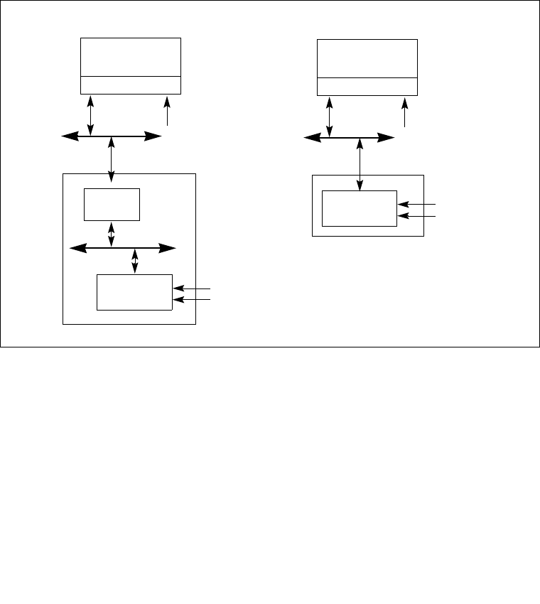
Vol. 3A 8-3
ADVANCED PROGRAMMABLE INTERRUPT CONTROLLER (APIC)
Xeon processors) or on the APIC bus (for Pentium and P6 family processors). See Section 8.2,
“System Bus Vs. APIC Bus.”
IPIs can be sent to other IA-32 processors in the system or to the originating processor (self-
interrupts). When the target processor receives an IPI message, its local APIC handles the
message automatically (using information included in the message such as vector number and
trigger mode). See Section 8.6, “Issuing Interprocessor Interrupts,” for a detailed explanation of
the local APIC’s IPI message delivery and acceptance mechanism.
The local APIC can also receive interrupts from externally connected devices through the I/O
APIC (see Figure 8-1). The I/O APIC is responsible for receiving interrupts generated by system
hardware and I/O devices and forwarding them to the local APIC as interrupt messages.
Individual pins on the I/O APIC can be programmed to generate a specific interrupt vector when
asserted. The I/O APIC also has a “virtual wire mode” that allows it to communicate with a stan-
dard 8259A-style external interrupt controller. Note that the local APIC can be disabled (see
Section 8.4.3, “Enabling or Disabling the Local APIC”). This allows an associated processor
core to receive interrupts directly from an 8259A interrupt controller.
Both the local APIC and the I/O APIC are designed to operate in MP systems (see Figures 8-2
and 8-3). Each local APIC handles interrupts from the I/O APIC, IPIs from processors on the
system bus, and self-generated interrupts. Interrupts can also be delivered to the individual
Figure 8-1. Relationship of Local APIC and I/O APIC In Single-Processor Systems
I/O APIC External
Interrupts
System Chip Set
System Bus
Processor Core
Local APIC
Pentium 4 and
Local
Interrupts
Bridge
PCI
Intel Xeon Processors
I/O APIC External
Interrupts
System Chip Set
3-Wire APIC Bus
Processor Core
Local APIC
Pentium and P6
Local
Interrupts
Family Processors
Interrupt
Messages Interrupt
Messages
Interrupt
Messages
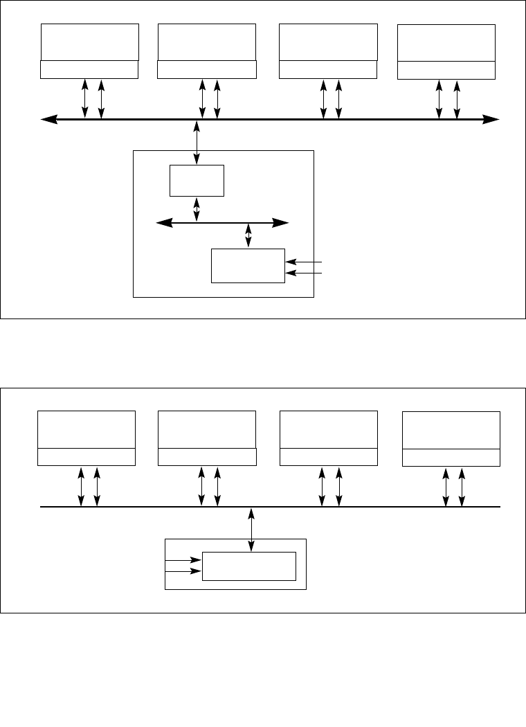
8-4 Vol. 3A
ADVANCED PROGRAMMABLE INTERRUPT CONTROLLER (APIC)
processors through the local interrupt pins; however, this mechanism is commonly not used in
MP systems.
Figure 8-2. Local APICs and I/O APIC When Intel Xeon Processors Are Used in Multiple-
Processor Systems
Figure 8-3. Local APICs and I/O APIC When P6 Family Processors Are Used in Multiple-
Processor Systems
I/O APIC External
Interrupts
System Chip Set
Processor System Bus
CPU
Local APIC
Processor #2
CPU
Local APIC
Processor #3
CPU
Local APIC
Processor #1
CPU
Local APIC
Processor #3
Bridge
PCI
IPIs IPIs IPIs
Interrupt
Messages
IPIs
Interrupt
Messages
Interrupt
Messages Interrupt
Messages
Interrupt
Messages
CPU
Local APIC
Processor #2
CPU
Local APIC
Processor #3
CPU
Local APIC
Processor #1
Interrupt
Messages
I/O APIC
External
Interrupts
System Chip Set
3-wire APIC Bus
CPU
Local APIC
Processor #4
IPIs
IPIs
IPIs
IPIs Interrupt
Messages
Interrupt
Messages
Interrupt
Messages
Interrupt
Messages

Vol. 3A 8-5
ADVANCED PROGRAMMABLE INTERRUPT CONTROLLER (APIC)
The IPI mechanism is typically used in MP systems to send fixed interrupts (interrupts for a
specific vector number) and special-purpose interrupts to processors on the system bus. For
example, a local APIC can use an IPI to forward a fixed interrupt to another processor for
servicing. Special-purpose IPIs (including NMI, INIT, SMI and SIPI IPIs) allow one or more
processors on the system bus to perform system-wide boot-up and control functions.
The following sections focus on the local APIC and its implementation in the Pentium 4, Intel
Xeon, and P6 family processors. In these sections, the terms “local APIC” and “I/O APIC” refer
to local and I/O APICs used with the P6 family processors and to local and I/O xAPICs used
with the Pentium 4 and Intel Xeon processors (see Section 8.3, “the Intel® 82489DX External
APIC, The APIC, and the xAPIC”).
8.2 SYSTEM BUS VS. APIC BUS
For the P6 family and Pentium processors, the I/O APIC and local APICs communicate through
the 3-wire inter-APIC bus (see Figure 8-3). Local APICs also use the APIC bus to send and
receive IPIs. The APIC bus and its messages are invisible to software and are not classed as
architectural.
Beginning with the Pentium 4 and Intel Xeon processors, the I/O APIC and local APICs (using
the xAPIC architecture) communicate through the system bus (see Figure 8-2). The I/O APIC
sends interrupt requests to the processors on the system bus through bridge hardware that is part
of the Intel chip set. The bridge hardware generates the interrupt messages that go to the local
APICs. IPIs between local APICs are transmitted directly on the system bus.
8.3 THE INTEL® 82489DX EXTERNAL APIC,
THE APIC, AND THE XAPIC
The local APIC in the P6 family and Pentium processors is an architectural subset of the Intel®
82489DX external APIC. See Section 17.26.1, “Software Visible Differences Between the
Local APIC and the 82489DX.”
The APIC architecture used in the Pentium 4 and Intel Xeon processors (called the xAPIC archi-
tecture) is an extension of the APIC architecture found in the P6 family processors. The primary
difference between the APIC and xAPIC architectures is that with the xAPIC architecture, the
local APICs and the I/O APIC communicate through the system bus. With the APIC architec-
ture, they communication through the APIC bus (see Section 8.2, “System Bus Vs. APIC Bus”).
Also, some APIC architectural features have been extended and/or modified in the xAPIC archi-
tecture. These extensions and modifications are noted in the following sections.
8.4 LOCAL APIC
The following sections describe the architecture of the local APIC and how to detect it, identify
it, and determine its status. Descriptions of how to program the local APIC are given in Section
8.5.1, “Local Vector Table,” and Section 8.6.1, “Interrupt Command Register (ICR).”

8-6 Vol. 3A
ADVANCED PROGRAMMABLE INTERRUPT CONTROLLER (APIC)
8.4.1 The Local APIC Block Diagram
Figure 8-4 gives a functional block diagram for the local APIC. Software interacts with the local
APIC by reading and writing its registers. APIC registers are memory-mapped to a 4-KByte
region of the processor’s physical address space with an initial starting address of FEE00000H.
For correct APIC operation, this address space must be mapped to an area of memory that has
been designated as strong uncacheable (UC). See Section 10.3, “Methods of Caching Available.”
In MP system configurations, the APIC registers for IA-32 processors on the system bus are
initially mapped to the same 4-KByte region of the physical address space. Software has the
option of changing initial mapping to a different 4-KByte region for all the local APICs or of
mapping the APIC registers for each local APIC to its own 4-KByte region. Section 8.4.5,
“Relocating the Local APIC Registers,” describes how to relocate the base address for APIC
registers.
NOTE
For P6 family, Pentium 4, and Intel Xeon processors, the APIC handles all
memory accesses to addresses within the 4-KByte APIC register space
internally and no external bus cycles are produced. For the Pentium
processors with an on-chip APIC, bus cycles are produced for accesses to the
APIC register space. Thus, for software intended to run on Pentium
processors, system software should explicitly not map the APIC register
space to regular system memory. Doing so can result in an invalid opcode
exception (#UD) being generated or unpredictable execution.
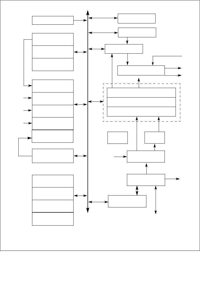
Vol. 3A 8-7
ADVANCED PROGRAMMABLE INTERRUPT CONTROLLER (APIC)
Figure 8-4. Local APIC Structure
Current Count
Register
Initial Count
Register
Divide Configuration
Register
Version Register
Error Status
Register
In-Service Register (ISR)
Vector
Decode
Interrupt Command
Register (ICR)
Acceptance
Logic
Vec[3:0]
& TMR Bit Register
Select
INIT
NMI
SMI
Protocol
Translation Logic
Dest. Mode
& Vector
Processor System Bus3
APIC ID
Register
Logical Destination
Register
Destination Format
Register
Timer
Local
Interrupts 0,1
Performance
Monitoring Counters1
Error
Timer
Local Vector Table
DATA/ADDR
Prioritizer
Task Priority Register
EOI Register
INTR
EXTINT
INTA
LINT0/1
1. Introduced in P6 family processors.
Thermal Sensor2
2. Introduced in the Pentium 4 and Intel Xeon processors.
Perf. Mon.
Thermal
(Internal
Interrupt)
Sensor
(Internal
Interrupt)
Spurious Vector
Register
Local
Interrupts
3. Three-wire APIC bus in P6 family and Pentium processors.
To
CPU
Core
From
CPU
Core
Interrupt Request Register (IRR)
Trigger Mode Register (TMR)
To
CPU
Core
Processor Priority
Register
4. Not implemented in Pentium 4 and Intel Xeon processors.
Arb. ID
Register4

8-8 Vol. 3A
ADVANCED PROGRAMMABLE INTERRUPT CONTROLLER (APIC)
Table 8-1 shows how the APIC registers are mapped into the 4-KByte APIC register space.
Registers are 32 bits, 64 bits, or 256 bits in width; all are aligned on 128-bit boundaries. All
32-bit registers should be accessed using 128-bit aligned 32-bit loads or stores. Some processors
may support loads and stores of less than 32 bits to some of the APIC registers. This is model
specific behavior and is not guaranteed to work on all processors. Wider registers (64-bit or 256-
bit) must be accessed using multiple 32-bit loads or stores, with the first access being 128-bit
aligned. If a LOCK prefix is used with a MOV instruction that accesses the APIC address space,
the prefix is ignored. The locking operation does not take place. All the registers listed in Table
8-1 are described in the following sections.
The local APIC registers listed in Table 8-1 are not MSRs. The only MSR associated with the
programming of the local APIC is the IA32_APIC_BASE MSR (see Section 8.4.3, “Enabling
or Disabling the Local APIC”).
Table 8-1. Local APIC Register Address Map
Address Register Name Software Read/Write
FEE0 0000H Reserved
FEE0 0010H Reserved
FEE0 0020H Local APIC ID Register Read/Write.
FEE0 0030H Local APIC Version Register Read Only.
FEE0 0040H Reserved
FEE0 0050H Reserved
FEE0 0060H Reserved
FEE0 0070H Reserved
FEE0 0080H Task Priority Register (TPR) Read/Write.
FEE0 0090H Arbitration Priority Register1 (APR) Read Only.
FEE0 00A0H Processor Priority Register (PPR) Read Only.
FEE0 00B0H EOI Register Write Only.
FEE0 00C0H Reserved
FEE0 00D0H Logical Destination Register Read/Write.
FEE0 00E0H Destination Format Register Bits 0-27 Read only; bits 28-31
Read/Write.
FEE0 00F0H Spurious Interrupt Vector Register Bits 0-8 Read/Write; bits 9-31
Read Only.
FEE0 0100H through
FEE0 0170H In-Service Register (ISR) Read Only.
FEE0 0180H through
FEE0 01F0H Trigger Mode Register (TMR) Read Only.
FEE0 0200H through
FEE0 0270H Interrupt Request Register (IRR) Read Only.
FEE0 0280H Error Status Register Read Only.

Vol. 3A 8-9
ADVANCED PROGRAMMABLE INTERRUPT CONTROLLER (APIC)
8.4.2 Presence of the Local APIC
Beginning with the P6 family processors, the presence or absence of an on-chip local APIC can
be detected using the CPUID instruction. When the CPUID instruction is executed with a source
operand of 1 in the EAX register, bit 9 of the CPUID feature flags returned in the EDX register
indicates the presence (set) or absence (clear) of a local APIC.
FEE0 0290H through
FEE0 02F0H Reserved
FEE0 0300H Interrupt Command Register (ICR) [0-31] Read/Write.
FEE0 0310H Interrupt Command Register (ICR) [32-63] Read/Write.
FEE0 0320H LVT Timer Register Read/Write.
FEE0 0330H LVT Thermal Sensor Register2Read/Write.
FEE0 0340H LVT Performance Monitoring Counters
Register3Read/Write.
FEE0 0350H LVT LINT0 Register Read/Write.
FEE0 0360H LVT LINT1 Register Read/Write.
FEE0 0370H LVT Error Register Read/Write.
FEE0 0380H Initial Count Register (for Timer) Read/Write.
FEE0 0390H Current Count Register (for Timer) Read Only.
FEE0 03A0H through
FEE0 03D0H Reserved
FEE0 03E0H Divide Configuration Register (for Timer) Read/Write.
FEE0 03F0H Reserved
NOTES:
1. Not supported in the Pentium 4 and Intel Xeon processors.
2. Introduced in the Pentium 4 and Intel Xeon processors. This APIC register and its associated function
are implementation dependent and may not be present in future IA-32 processors.
3. Introduced in the Pentium Pro processor. This APIC register and its associated function are implemen-
tation dependent and may not be present in future IA-32 processors.
Table 8-1. Local APIC Register Address Map (Contd.)
Address Register Name Software Read/Write

8-10 Vol. 3A
ADVANCED PROGRAMMABLE INTERRUPT CONTROLLER (APIC)
8.4.3 Enabling or Disabling the Local APIC
The local APIC can be enabled or disabled in either of two ways:
1. Using the APIC global enable/disable flag in the IA32_APIC_BASE MSR (MSR address
1BH; see Figure 8-5):
— When IA32_APIC_BASE[11] is 0, the processor is functionally equivalent to an
IA-32 processor without an on-chip APIC. The CPUID feature flag for the APIC (see
Section 8.4.2, “Presence of the Local APIC”) is also set to 0.
— When IA32_APIC_BASE[11] is set to 0, processor APICs based on the 3-wire APIC
bus cannot be generally re-enabled until a system hardware reset. The 3-wire bus
looses track of arbitration that would be necessary for complete re-enabling. Certain
APIC functionality can be enabled (for example: performance and thermal monitoring
interrupt generation).
— For processors that use Front Side Bus (FSB) delivery of interrupts, software may
disable or enable the APIC by setting and resetting IA32_APIC_BASE[11]. A
hardware reset is not required to re-start APIC functionality.
— When IA32_APIC_BASE[11] is set to 0, prior initialization to the APIC may be lost
and the APIC may return to the state described in Section 8.4.7.1, “Local APIC State
After Power-Up or Reset.”
2. Using the APIC software enable/disable flag in the spurious-interrupt vector register (see
Figure 8-23):
— If IA32_APIC_BASE[11] is 1, software can temporarily disable a local APIC at any
time by clearing the APIC software enable/disable flag in the spurious-interrupt vector
register (see Figure 8-23). The state of the local APIC when in this software-disabled
state is described in Section 8.4.7.2, “Local APIC State After It Has Been Software
Disabled.”
— When the local APIC is in the software-disabled state, it can be re-enabled at any time
by setting the APIC software enable/disable flag to 1.
For the Pentium processor, the APICEN pin (which is shared with the PICD1 pin) is used during
power-up or RESET to disable the local APIC.
Note that each entry in the LVT has a mask bit that can be used to inhibit interrupts from being
delivered to the processor from selected local interrupt sources (the LINT0 and LINT1 pins, the
APIC timer, the performance-monitoring counters, the thermal sensor, and/or the internal APIC
error detector).
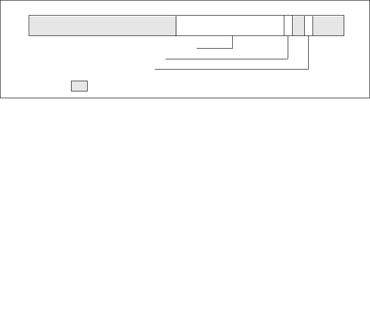
Vol. 3A 8-11
ADVANCED PROGRAMMABLE INTERRUPT CONTROLLER (APIC)
8.4.4 Local APIC Status and Location
The status and location of the local APIC are contained in the IA32_APIC_BASE MSR (see
Figure 8-5). MSR bit functions are described below:
•BSP flag, bit 8 ⎯ Indicates if the processor is the bootstrap processor (BSP). See Section
7.5, “Multiple-Processor (MP) Initialization.” Following a power-up or RESET, this flag is
set to 1 for the processor selected as the BSP and set to 0 for the remaining processors
(APs).
•APIC Global Enable flag, bit 11 ⎯ Enables or disables the local APIC (see Section 8.4.3,
“Enabling or Disabling the Local APIC”). This flag is available in the Pentium 4, Intel
Xeon, and P6 family processors. It is not guaranteed to be available or available at the
same location in future IA-32 processors.
•APIC Base field, bits 12 through 35 ⎯ Specifies the base address of the APIC registers.
This 24-bit value is extended by 12 bits at the low end to form the base address. This
automatically aligns the address on a 4-KByte boundary. Following a power-up or RESET,
the field is set to FEE0 0000H.
•Bits 0 through 7, bits 9 and 10, and bits 36 through 63 in the IA32_APIC_BASE MSR are
reserved.
8.4.5 Relocating the Local APIC Registers
The Pentium 4, Intel Xeon, and P6 family processors permit the starting address of the APIC
registers to be relocated from FEE00000H to another physical address by modifying the value
in the 24-bit base address field of the IA32_APIC_BASE MSR. This extension of the APIC
architecture is provided to help resolve conflicts with memory maps of existing systems and to
allow individual processors in an MP system to map their APIC registers to different locations
in physical memory.
Figure 8-5. IA32_APIC_BASE MSR (APIC_BASE_MSR in P6 Family)
BSP—Processor is BSP
APIC global enable/disable
APIC Base—Base physical address
63 071011 8912
Reserved
36 35
APIC Base
Reserved

8-12 Vol. 3A
ADVANCED PROGRAMMABLE INTERRUPT CONTROLLER (APIC)
8.4.6 Local APIC ID
At power up, system hardware assigns a unique APIC ID to each local APIC on the system bus
(for Pentium 4 and Intel Xeon processors) or on the APIC bus (for P6 family and Pentium
processors). The hardware assigned APIC ID is based on system topology and includes
encoding for socket position and cluster information (see Figure 7-2).
In MP systems, the local APIC ID is also used as a processor ID by the BIOS and the operating
system. Some processors permit software to modify the APIC ID. However, the ability of soft-
ware to modify the APIC ID is processor model specific. Because of this, operating system soft-
ware should avoid writing to the local APIC ID register. The value returned by bits 31-24 of the
EBX register (when the CPUID instruction is executed with a source operand value of 1 in the
EAX register) is always the Initial APIC ID (determined by the platform initialization). This is
true even if software has changed the value in the Local APIC ID register.
The processor receives the hardware assigned APIC ID (or Initial APIC ID) by sampling pins
A11# and A12# and pins BR0# through BR3# (for the Pentium 4, Intel Xeon, and P6 family
processors) and pins BE0# through BE3# (for the Pentium processor). The APIC ID latched
from these pins is stored in the APIC ID field of the local APIC ID register (see Figure 8-6), and
is used as the Initial APIC ID for the processor.
For the P6 family and Pentium processors, the local APIC ID field in the local APIC ID register
is 4 bits. Encodings 0H through EH can be used to uniquely identify 15 different processors
connected to the APIC bus. For the Pentium 4 and Intel Xeon processors, the xAPIC specifica-
tion extends the local APIC ID field to 8 bits. These can be used to identify up to 255 processors
in the system.
8.4.7 Local APIC State
The following sections describe the state of the local APIC and its registers following a power-
up or RESET, after the local APIC has been software disabled, following an INIT reset, and
following an INIT-deassert message.
Figure 8-6. Local APIC ID Register
31 0
2324
ReservedAPIC ID*
Address: 0FEE0 0020H
Value after reset: 0000 0000H
* For the P6 family and Pentium processors,
bits 28-31 are reserved. For Pentium 4
and Xeon processors, 21-31 are reserved.

Vol. 3A 8-13
ADVANCED PROGRAMMABLE INTERRUPT CONTROLLER (APIC)
8.4.7.1 Local APIC State After Power-Up or Reset
Following a power-up or RESET of the processor, the state of local APIC and its registers are
as follows:
•The following registers are reset to all 0s:
•IRR, ISR, TMR, ICR, LDR, and TPR
•Timer initial count and timer current count registers
•Divide configuration register
•The DFR register is reset to all 1s.
•The LVT register is reset to 0s except for the mask bits; these are set to 1s.
•The local APIC version register is not affected.
•The local APIC ID register is set to a unique APIC ID. (Pentium and P6 family processors
only). The Arb ID register is set to the value in the APIC ID register.
•The spurious-interrupt vector register is initialized to 000000FFH. By setting bit 8 to 0,
software disables the local APIC.
•If the processor is the only processor in the system or it is the BSP in an MP system (see
Section 7.5.1, “BSP and AP Processors”); the local APIC will respond normally to INIT
and NMI messages, to INIT# signals and to STPCLK# signals. If the processor is in an MP
system and has been designated as an AP; the local APIC will respond the same as for the
BSP. In addition, it will respond to SIPI messages. For P6 family processors only, an AP
will not respond to a STPCLK# signal.
8.4.7.2 Local APIC State After It Has Been Software Disabled
When the APIC software enable/disable flag in the spurious interrupt vector register has been
explicitly cleared (as opposed to being cleared during a power up or RESET), the local APIC is
temporarily disabled (see Section 8.4.3, “Enabling or Disabling the Local APIC”). The opera-
tion and response of a local APIC while in this software-disabled state is as follows:
•The local APIC will respond normally to INIT, NMI, SMI, and SIPI messages.
•Pending interrupts in the IRR and ISR registers are held and require masking or handling
by the CPU.
•The local APIC can still issue IPIs. It is software’s responsibility to avoid issuing IPIs
through the IPI mechanism and the ICR register if sending interrupts through this
mechanism is not desired.
•The reception or transmission of any IPIs that are in progress when the local APIC is
disabled are completed before the local APIC enters the software-disabled state.
•The mask bits for all the LVT entries are set. Attempts to reset these bits will be ignored.
•(For Pentium and P6 family processors) The local APIC continues to listen to all bus
messages in order to keep its arbitration ID synchronized with the rest of the system.

8-14 Vol. 3A
ADVANCED PROGRAMMABLE INTERRUPT CONTROLLER (APIC)
8.4.7.3 Local APIC State After an INIT Reset (“Wait-for-SIPI” State)
An INIT reset of the processor can be initiated in either of two ways:
•By asserting the processor’s INIT# pin.
•By sending the processor an INIT IPI (an IPI with the delivery mode set to INIT).
Upon receiving an INIT through either of these mechanisms, the processor responds by begin-
ning the initialization process of the processor core and the local APIC. The state of the local
APIC following an INIT reset is the same as it is after a power-up or hardware RESET, except
that the APIC ID and arbitration ID registers are not affected. This state is also referred to at the
“wait-for-SIPI” state (see also: Section 7.5.2, “MP Initialization Protocol Requirements and
Restrictions for Intel Xeon Processors”).
8.4.7.4 Local APIC State After It Receives an INIT-Deassert IPI
Only the Pentium and P6 family processors support the INIT-deassert IPI. An INIT-disassert IPI
has no affect on the state of the APIC, other than to reload the arbitration ID register with the
value in the APIC ID register.
8.4.8 Local APIC Version Register
The local APIC contains a hardwired version register. Software can use this register to identify
the APIC version (see Figure 8-7). In addition, the register specifies the number of entries in the
local vector table (LVT) for a specific implementation.
The fields in the local APIC version register are as follows:
Version The version numbers of the local APIC:
1XH Local APIC. For Pentium 4 and Intel Xeon proces-
sors, 14H is returned.
0XH 82489DX external APIC.
20H through FFHReserved.
Max LVT Entry Shows the number of LVT entries minus 1. For the Pentium 4 and Intel
Xeon processors (which have 6 LVT entries), the value returned in the
Max LVT field is 5; for the P6 family processors (which have 5 LVT
entries), the value returned is 4; for the Pentium processor (which has
4 LVT entries), the value returned is 3.

Vol. 3A 8-15
ADVANCED PROGRAMMABLE INTERRUPT CONTROLLER (APIC)
8.5 HANDLING LOCAL INTERRUPTS
The following sections describe facilities that are provided in the local APIC for handling local
interrupts. These include: the processor’s LINT0 and LINT1 pins, the APIC timer, the perfor-
mance-monitoring counters, the thermal sensor, and the internal APIC error detector. Local
interrupt handling facilities include: the LVT, the error status register (ESR), the divide config-
uration register (DCR), and the initial count and current count registers.
8.5.1 Local Vector Table
The local vector table (LVT) allows software to specify the manner in which the local interrupts
are delivered to the processor core. It consists of the following five 32-bit APIC registers (see
Figure 8-8), one for each local interrupt:
•LVT Timer Register (FEE0 0320H) — Specifies interrupt delivery when the APIC timer
signals an interrupt (see Section 8.5.4, “APIC Timer”).
•LVT Thermal Monitor Register (FEE0 0330H) — Specifies interrupt delivery when the
thermal sensor generates an interrupt (see Section 13.4.2, “Thermal Monitor”). This LVT
entry is implementation specific, not architectural. If implemented, it will always be at
base address FEE0 0330H.
•LVT Performance Counter Register (FEE0 0340H) — Specifies interrupt delivery
when a performance counter generates an interrupt on overflow (see Section 18.13.6.9,
“Generating an Interrupt on Overflow”). This LVT entry is implementation specific, not
architectural. If implemented, it is not guaranteed to be at base address FEE0 0340H.
•LVT LINT0 Register (FEE0 0350H) — Specifies interrupt delivery when an interrupt is
signaled at the LINT0 pin.
•LVT LINT1 Register (FEE0 0360H) — Specifies interrupt delivery when an interrupt is
signaled at the LINT1 pin.
•LVT Error Register (FEE0 0370H) — Specifies interrupt delivery when the APIC
detects an internal error (see Section 8.5.3, “Error Handling”).
The LVT performance counter register and its associated interrupt were introduced in the P6
processors and are also present in the Pentium 4 and Intel Xeon processors. The LVT thermal
Figure 8-7. Local APIC Version Register
31 0
Reserved
2324 15
Version
Max. LVT
Value after reset: 000N 00VVH
V = Version, N = # of LVT entries minus 1
Entry
7
Address: FEE0 0030H
16 8
Reserved
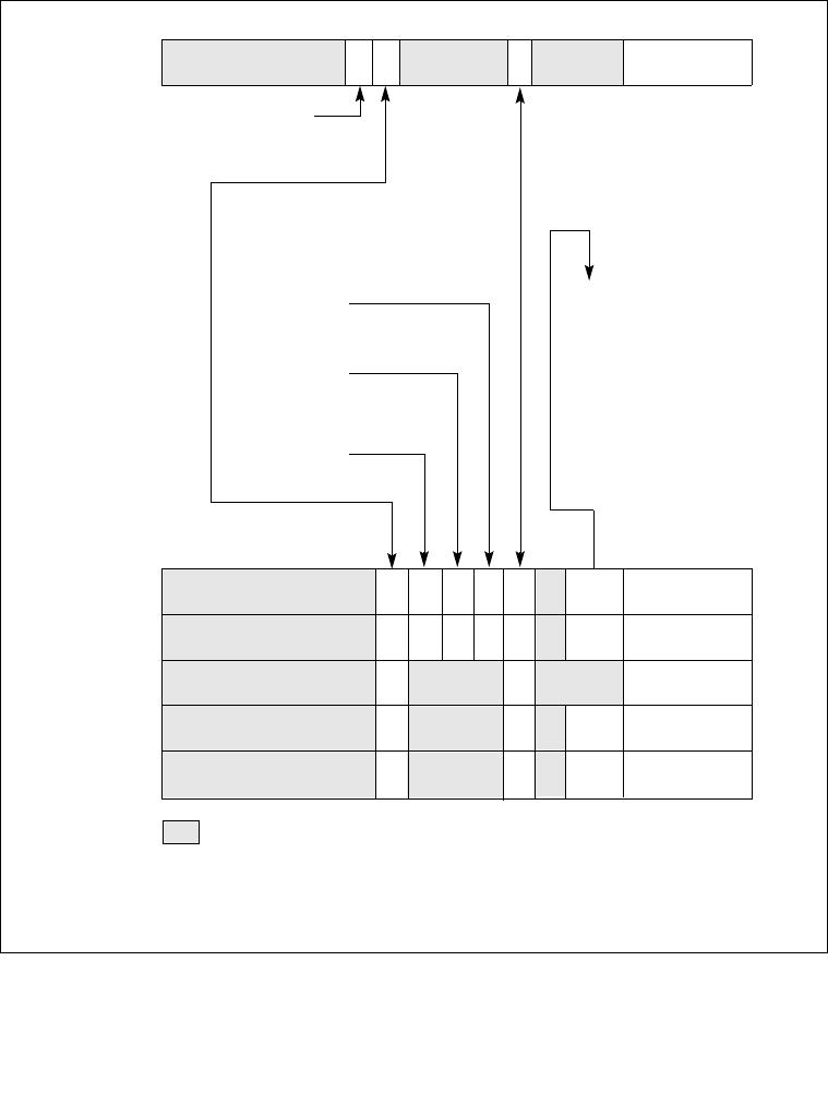
8-16 Vol. 3A
ADVANCED PROGRAMMABLE INTERRUPT CONTROLLER (APIC)
monitor register and its associated interrupt were introduced in the Pentium 4 and Intel Xeon
processors.
As shown in Figures 8-8, some of these fields and flags are not available (and reserved) for some
entries.
Figure 8-8. Local Vector Table (LVT)
31 07
Vector
Timer Mode
0: One-shot
1: Periodic
1215161718
Delivery Mode
000: Fixed
100: NMI
Mask†
0: Not Masked
1: Masked
Address: FEE0 0350H
Value After Reset: 0001 0000H
Reserved
12131516
Vector
31 07810
Address: FEE0 0360H
Address: FEE0 0370H
Vector
Vector
Error
LINT1
LINT0
Value after Reset: 0001 0000H
Address: FEE0 0320H
111: ExtlNT
All other combinations
are Reserved
Interrupt Input
Pin Polarity
Trigger Mode
0: Edge
1: Level
Remote
IRR
Delivery Status
0: Idle
1: Send Pending
Timer
13 11 8
11
14
17
Address: FEE0 0340H
Performance Vector
Thermal Vector
Mon. Counters
Sensor
Address: FEE0 0330H
† (Pentium 4 and Intel Xeon processors.) When a
performance monitoring counters interrupt is generated,
the mask bit for its associated LVT entry is set.
010: SMI
101: INIT

Vol. 3A 8-17
ADVANCED PROGRAMMABLE INTERRUPT CONTROLLER (APIC)
The setup information that can be specified in the registers of the LVT table is as follows:
Vector Interrupt vector number.
Delivery Mode Specifies the type of interrupt to be sent to the processor. Some
delivery modes will only operate as intended when used in conjunc-
tion with a specific trigger mode. The allowable delivery modes are
as follows:
000 (Fixed) Delivers the interrupt specified in the vector field.
010 (SMI) Delivers an SMI interrupt to the processor core
through the processor’s local SMI signal path.
When using this delivery mode, the vector field
should be set to 00H for future compatibility.
100 (NMI) Delivers an NMI interrupt to the processor. The
vector information is ignored.
101 (INIT) Delivers an INIT request to the processor core,
which causes the processor to perform an INIT.
When using this delivery mode, the vector field
should be set to 00H for future compatibility.
111 (ExtINT) Causes the processor to respond to the interrupt as
if the interrupt originated in an externally connect-
ed (8259A-compatible) interrupt controller. A
special INTA bus cycle corresponding to ExtINT,
is routed to the external controller. The external
controller is expected to supply the vector infor-
mation. The APIC architecture supports only one
ExtINT source in a system, usually contained in
the compatibility bridge.
Delivery Status (Read Only)
Indicates the interrupt delivery status, as follows:
0 (Idle) There is currently no activity for this interrupt
source, or the previous interrupt from this source
was delivered to the processor core and accepted.
1 (Send Pending)Indicates that an interrupt from this source has
been delivered to the processor core, but has not
yet been accepted (see Section 8.5.5, “Local Inter-
rupt Acceptance”).
Interrupt Input Pin Polarity
Specifies the polarity of the corresponding interrupt pin: (0) active
high or (1) active low.

8-18 Vol. 3A
ADVANCED PROGRAMMABLE INTERRUPT CONTROLLER (APIC)
Remote IRR Flag (Read Only)
For fixed mode, level-triggered interrupts; this flag is set when the
local APIC accepts the interrupt for servicing and is reset when an
EOI command is received from the processor. The meaning of this
flag is undefined for edge-triggered interrupts and other delivery
modes.
Trigger Mode Selects the trigger mode for the local LINT0 and LINT1 pins: (0)
edge sensitive and (1) level sensitive. This flag is only used when the
delivery mode is Fixed. When the delivery mode is NMI, SMI, or
INIT, the trigger mode is always edge sensitive. When the delivery
mode is ExtINT, the trigger mode is always level sensitive. The timer
and error interrupts are always treated as edge sensitive.
If the local APIC is not used in conjunction with an I/O APIC and
fixed delivery mode is selected; the Pentium 4, Intel Xeon, and P6
family processors will always use level-sensitive triggering, regard-
less if edge-sensitive triggering is selected.
Mask Interrupt mask: (0) enables reception of the interrupt and (1) inhibits
reception of the interrupt. When the local APIC handles a perfor-
mance-monitoring counters interrupt, it automatically sets the mask
flag in the corresponding LVT entry. This flag will remain set until
software clears it.
Timer Mode Selects the timer mode: (0) one-shot and (1) periodic (see Section
8.5.4, “APIC Timer”).
8.5.2 Valid Interrupt Vectors
The IA-32 architecture defines 256 vector numbers, ranging from 0 through 255 (see Section 5.2,
“Exception and Interrupt Vectors”). Local and I/O APICs support 240 of these vectors (in the
range of 16 to 255) as valid interrupts.
When an interrupt vector in the range of 0 to 15 is sent or received through the local APIC, the
APIC indicates an illegal vector in its Error Status Register (see Section 8.5.3, “Error
Handling”). The IA-32 architecture reserves vectors 16 through 31 for predefined interrupts,
exceptions, and Intel-reserved encodings (see Table 5-1). However, the local APIC does not
treat vectors in this range as illegal.
When an illegal vector value (0 to 15) is written to an LVT entry and the delivery mode is Fixed
(bits 8-11 equal 0), the APIC may signal an illegal vector error, without regard to whether the
mask bit is set or whether an interrupt is actually seen on the input.

Vol. 3A 8-19
ADVANCED PROGRAMMABLE INTERRUPT CONTROLLER (APIC)
8.5.3 Error Handling
The local APIC provides an error status register (ESR) that it uses to record errors that it detects
when handling interrupts (see Figure 8-9). An APIC error interrupt is generated when the local
APIC sets one of the error bits in the ESR. The LVT error register allows selection of the inter-
rupt vector to be delivered to the processor core when APIC error is detected. The LVT error
register also provides a means of masking an APIC error interrupt.
The functions of the ESR are listed in Table 8-2.
Table 8-2. ESR Flags
FLAG Function
Send Checksum Error (P6 family and Pentium processors only) Set when the local APIC detects
a checksum error for a message that it sent on the APIC bus.
Receive Checksum Error (P6 family and Pentium processors only) Set when the local APIC detects
a checksum error for a message that it received on the APIC bus.
Send Accept Error (P6 family and Pentium processors only) Set when the local APIC detects
that a message it sent was not accepted by any APIC on the APIC bus.
Receive Accept Error (P6 family and Pentium processors only) Set when the local APIC detects
that the message it received was not accepted by any APIC on the APIC
bus, including itself.
Send Illegal Vector Set when the local APIC detects an illegal vector in the message that it is
sending.
Receive Illegal Vector Set when the local APIC detects an illegal vector in the message it
received, including an illegal vector code in the local vector table
interrupts or in a self-interrupt.
Illegal Reg. Address (Pentium 4, Intel Xeon, and P6 family processors only) Set when the
processor is trying to access a register that is not implemented in the
processors’ local APIC register address space; that is, within the address
range of the APIC register base address (specified in the
IA32_APIC_BASE MSR) plus 4K Bytes.

8-20 Vol. 3A
ADVANCED PROGRAMMABLE INTERRUPT CONTROLLER (APIC)
The ESR is a write/read register. A write (of any value) to the ESR must be done just prior to
reading the ESR to update the register. This initial write causes the ESR contents to be updated
with the latest error status. Back-to-back writes clear the ESR register.
After an error bit is set in the register, it remains set until the register is cleared. Setting the mask
bit for the LVT error register prevents errors from being recorded in the ESR; however, the state
of the ESR before the mask bit was set is maintained.
8.5.4 APIC Timer
The local APIC unit contains a 32-bit programmable timer that is available to software to time
events or operations. This timer is set up by programming four registers: the divide configura-
tion register (see Figure 8-10), the initial-count and current-count registers (see Figure 8-11),
and the LVT timer register (see Figure 8-8).
Figure 8-9. Error Status Register (ESR)
Address: FEE0 0280H
Value after reset: 0H
31 0
Reserved
78123456
Illegal Register Address1
Received Illegal Vector
Send Illegal Vector
Reserved
Receive Accept Error2
Send Accept Error2
Receive Checksum Error2
Send Checksum Error2
2. Only used in the P6 family and Pentium processors;
reserved in the Pentium 4 and Intel Xeon processors.
1. Only used in the Pentium 4, Intel Xeon, and P6 family
processors; reserved in the Pentium processor.
NOTES:
Vol. 3A 8-21
ADVANCED PROGRAMMABLE INTERRUPT CONTROLLER (APIC)
The time base for the timer is derived from the processor’s bus clock, divided by the value spec-
ified in the divide configuration register.
The timer can be configured through the timer LVT entry for one-shot or periodic operation. In
one-shot mode, the timer is started by programming its initial-count register. The initial count
value is then copied into the current-count register and count-down begins. After the timer
reaches zero, an timer interrupt is generated and the timer remains at its 0 value until repro-
grammed.
In periodic mode, the current-count register is automatically reloaded from the initial-count
register when the count reaches 0 and a timer interrupt is generated, and the count-down is
repeated. If during the count-down process the initial-count register is set, counting will restart,
using the new initial-count value. The initial-count register is a read-write register; the current-
count register is read only.
The LVT timer register determines the vector number that is delivered to the processor with the
timer interrupt that is generated when the timer count reaches zero. The mask flag in the LVT
timer register can be used to mask the timer interrupt.
Figure 8-10. Divide Configuration Register
Figure 8-11. Initial Count and Current Count Registers
Address: FEE0 03E0H
Value after reset: 0H
0
Divide Value (bits 0, 1 and 3)
000: Divide by 2
001: Divide by 4
010: Divide by 8
011: Divide by 16
100: Divide by 32
101: Divide by 64
110: Divide by 128
111: Divide by 1
31 0
Reserved
1234
31 0
Initial Count
Address: Initial Count
Value after reset: 0H
Current Count
Current Count FEE0 0390H
FEE0 0380H

8-22 Vol. 3A
ADVANCED PROGRAMMABLE INTERRUPT CONTROLLER (APIC)
8.5.5 Local Interrupt Acceptance
When a local interrupt is sent to the processor core, it is subject to the acceptance criteria spec-
ified in the interrupt acceptance flow chart in Figure 8-17. If the interrupt is accepted, it is logged
into the IRR register and handled by the processor according to its priority (see Section 8.8.4,
“Interrupt Acceptance for Fixed Interrupts”). If the interrupt is not accepted, it is sent back to
the local APIC and retried.
8.6 ISSUING INTERPROCESSOR INTERRUPTS
The following sections describe the local APIC facilities that are provided for issuing interpro-
cessor interrupts (IPIs) from software. The primary local APIC facility for issuing IPIs is the
interrupt command register (ICR). The ICR can be used for the following functions:
•To send an interrupt to another processor.
•To allow a processor to forward an interrupt that it received but did not service to another
processor for servicing.
•To direct the processor to interrupt itself (perform a self interrupt).
•To deliver special IPIs, such as the start-up IPI (SIPI) message, to other processors.
Interrupts generated with this facility are delivered to the other processors in the system through
the system bus (for Pentium 4 and Intel Xeon processors) or the APIC bus (for P6 family and
Pentium processors). The ability for a processor to send a lowest priority IPI is model specific
and should be avoided by BIOS and operating system software.
8.6.1 Interrupt Command Register (ICR)
The interrupt command register (ICR) is a 64-bit local APIC register (see Figure 8-12) that
allows software running on the processor to specify and send interprocessor interrupts (IPIs) to
other IA-32 processors in the system.
To send an IPI, software must set up the ICR to indicate the type of IPI message to be sent and
the destination processor or processors. (All fields of the ICR are read-write by software with
the exception of the delivery status field, which is read-only.) The act of writing to the low
doubleword of the ICR causes the IPI to be sent.
Vol. 3A 8-23
ADVANCED PROGRAMMABLE INTERRUPT CONTROLLER (APIC)
The ICR consists of the following fields.
Vector The vector number of the interrupt being sent.
Delivery Mode Specifies the type of IPI to be sent. This field is also know as the IPI
message type field.
000 (Fixed) Delivers the interrupt specified in the vector field
to the target processor or processors.
001 (Lowest Priority)
Same as fixed mode, except that the interrupt is
delivered to the processor executing at the lowest
priority among the set of processors specified in
the destination field. The ability for a processor to
Figure 8-12. Interrupt Command Register (ICR)
31 0
Reserved
7
Vector
Destination Shorthand
810
Delivery Mode
000: Fixed
001: Lowest Priority1
00: No Shorthand
01: Self
111213141516171819
10: All Including Self
11: All Excluding Self 010: SMI
011: Reserved
100: NMI
101: INIT
110: Start Up
111: Reserved
Destination Mode
0: Physical
1: Logical
Delivery Status
0: Idle
1: Send Pending
Level
0 = De-assert
1 = Assert
Trigger Mode
0: Edge
1: Level
63 32
Reserved
Destination Field
56
Address: FEE0 0300H (0 - 31)
Value after Reset: 0H
Reserved
20
55
FEE0 0310H (32 - 63)
NOTE:
1. The ability of a processor to send Lowest Priority IPI is model specific.

8-24 Vol. 3A
ADVANCED PROGRAMMABLE INTERRUPT CONTROLLER (APIC)
send a lowest priority IPI is model specific and
should be avoided by BIOS and operating system
software.
010 (SMI) Delivers an SMI interrupt to the target processor
or processors. The vector field must be pro-
grammed to 00H for future compatibility.
011 (Reserved)
100 (NMI) Delivers an NMI interrupt to the target processor
or processors. The vector information is ignored.
101 (INIT) Delivers an INIT request to the target processor or
processors, which causes them to perform an
INIT. As a result of this IPI message, all the target
processors perform an INIT. The vector field must
be programmed to 00H for future compatibility.
101 (INIT Level De-assert)
(Not supported in the Pentium 4 and Intel Xeon
processors.) Sends a synchronization message to
all the local APICs in the system to set their arbi-
tration IDs (stored in their Arb ID registers) to the
values of their APIC IDs (see Section 8.7, “Sys-
tem and APIC Bus Arbitration”). For this delivery
mode, the level flag must be set to 0 and trigger
mode flag to 1. This IPI is sent to all processors,
regardless of the value in the destination field or
the destination shorthand field; however, software
should specify the “all including self” shorthand.
110 (Start-Up) Sends a special “start-up” IPI (called a SIPI) to the
target processor or processors. The vector typical-
ly points to a start-up routine that is part of the
BIOS boot-strap code (see Section 7.5, “Multiple-
Processor (MP) Initialization”). IPIs sent with this
delivery mode are not automatically retried if the
source APIC is unable to deliver it. It is up to the
software to determine if the SIPI was not success-
fully delivered and to reissue the SIPI if necessary.

Vol. 3A 8-25
ADVANCED PROGRAMMABLE INTERRUPT CONTROLLER (APIC)
Destination Mode Selects either physical (0) or logical (1) destination mode (see
Section 8.6.2, “Determining IPI Destination”).
Delivery Status (Read Only)
Indicates the IPI delivery status, as follows:
0 (Idle) There is currently no IPI activity for this local
APIC, or the previous IPI sent from this local
APIC was delivered and accepted by the target
processor or processors.
1 (Send Pending)Indicates that the last IPI sent from this local APIC
has not yet been accepted by the target processor
or processors.
Level For the INIT level de-assert delivery mode this flag must be set to 0;
for all other delivery modes it must be set to 1. (This flag has no
meaning in Pentium 4 and Intel Xeon processors, and will always be
issued as a 1.)
Trigger Mode Selects the trigger mode when using the INIT level de-assert delivery
mode: edge (0) or level (1). It is ignored for all other delivery modes.
(This flag has no meaning in Pentium 4 and Intel Xeon processors,
and will always be issued as a 0.)
Destination Shorthand Indicates whether a shorthand notation is used to specify the destina-
tion of the interrupt and, if so, which shorthand is used. Destination
shorthands are used in place of the 8-bit destination field, and can be
sent by software using a single write to the low doubleword of the
ICR. Shorthands are defined for the following cases: software self
interrupt, IPIs to all processors in the system including the sender,
IPIs to all processors in the system excluding the sender.
00: (No Shorthand)
The destination is specified in the destination field.
01: (Self) The issuing APIC is the one and only destination
of the IPI. This destination shorthand allows soft-
ware to interrupt the processor on which it is exe-
cuting. An APIC implementation is free to deliver
the self-interrupt message internally or to issue the
message to the bus and “snoop” it as with any other
IPI message.
10: (All Including Self)
The IPI is sent to all processors in the system in-
cluding the processor sending the IPI. The APIC
will broadcast an IPI message with the destination
field set to FH for Pentium and P6 family proces-

8-26 Vol. 3A
ADVANCED PROGRAMMABLE INTERRUPT CONTROLLER (APIC)
sors and to FFH for Pentium 4 and Intel Xeon pro-
cessors.
11: (All Excluding Self)
The IPI is sent to all processors in a system with
the exception of the processor sending the IPI. The
APIC broadcasts a message with the physical des-
tination mode and destination field set to 0xFH for
Pentium and P6 family processors and to 0xFFH
for Pentium 4 and Intel Xeon processors. Support
for this destination shorthand in conjunction with
the lowest-priority delivery mode is model specif-
ic. For Pentium 4 and Intel Xeon processors, when
this shorthand is used together with lowest priority
delivery mode, the IPI may be redirected back to
the issuing processor.
Destination Specifies the target processor or processors. This field is only used
when the destination shorthand field is set to 00B. If the destination
mode is set to physical, then bits 56 through 59 contain the APIC ID
of the target processor for Pentium and P6 family processors and bits
56 through 63 contain the APIC ID of the target processor the for
Pentium 4 and Intel Xeon processors. If the destination mode is set
to logical, the interpretation of the 8-bit destination field depends on
the settings of the DFR and LDR registers of the local APICs in all
the processors in the system (see Section 8.6.2, “Determining IPI
Destination”).
Not all combinations of options for the ICR are valid. Table 8-3 shows the valid combinations
for the fields in the ICR for the Pentium 4 and Intel Xeon processors; Table 8-4 shows the valid
combinations for the fields in the ICR for the P6 family processors. Also note that the lower half
of the ICR may not be preserved over transitions to the deepest C-States.
Table 8-3. Valid Combinations for the Pentium 4 and Intel Xeon Processors’
Local xAPIC Interrupt Command Register
Destination
Shorthand Valid/
Invalid Trigger
Mode Delivery Mode Destination Mode
No Shorthand Valid Edge All Modes1Physical or Logical
No Shorthand Invalid2Level All Modes Physical or Logical
Self Valid Edge Fixed X3
Self Invalid2Level Fixed X
Self Invalid X Lowest Priority, NMI, INIT, SMI, Start-Up X
All Including Self Valid Edge Fixed X
All Including Self Invalid2Level Fixed X
All Including Self Invalid X Lowest Priority, NMI, INIT, SMI, Start-Up X

Vol. 3A 8-27
ADVANCED PROGRAMMABLE INTERRUPT CONTROLLER (APIC)
All Excluding Self Valid Edge Fixed, Lowest Priority1,4, NMI, INIT, SMI,
Start-Up X
All Excluding Self Invalid2Level FIxed, Lowest Priority4, NMI, INIT, SMI,
Start-Up X
NOTES:
1. The ability of a processor to send a lowest priority IPI is model specific.
2. For these interrupts, if the trigger mode bit is 1 (Level), the local xAPIC will override the bit setting and
issue the interrupt as an edge triggered interrupt.
3. X means the setting is ignored.
4. When using the “lowest priority” delivery mode and the “all excluding self” destination, the IPI can be
redirected back to the issuing APIC, which is essentially the same as the “all including self” destination
mode.
Table 8-4. Valid Combinations for the P6 Family Processors’
Local APIC Interrupt Command Register
Destination
Shorthand Valid/
Invalid Trigger
Mode Delivery Mode Destination Mode
No Shorthand Valid Edge All Modes1Physical or Logical
No Shorthand Valid2Level Fixed, Lowest Priority1, NMI Physical or Logical
No Shorthand Valid3Level INIT Physical or Logical
Self Valid Edge Fixed X4
Self 1 Level Fixed X
Self Invalid5X Lowest Priority, NMI, INIT, SMI,
Start-Up X
All including Self Valid Edge Fixed X
All including Self Valid2Level Fixed X
All including Self Invalid5X Lowest Priority, NMI, INIT, SMI,
Start-Up X
All excluding Self Valid Edge All Modes1X
All excluding Self Valid2Level Fixed, Lowest Priority1, NMI X
All excluding Self Invalid5Level SMI, Start-Up X
All excluding Self Valid3Level INIT X
X Invalid5Level SMI, Start-Up X
NOTES:
1. The ability of a processor to send a lowest priority IPI is model specific.
2. Treated as edge triggered if level bit is set to 1, otherwise ignored.
3. Treated as edge triggered when Level bit is set to 1; treated as “INIT Level Deassert” message when
level bit is set to 0 (deassert). Only INIT level deassert messages are allowed to have the level bit set to
0. For all other messages the level bit must be set to 1.
4. X means the setting is ignored.
5. The behavior of the APIC is undefined.
Table 8-3. Valid Combinations for the Pentium 4 and Intel Xeon Processors’
Local xAPIC Interrupt Command Register (Contd.)
Destination
Shorthand Valid/
Invalid Trigger
Mode Delivery Mode Destination Mode

8-28 Vol. 3A
ADVANCED PROGRAMMABLE INTERRUPT CONTROLLER (APIC)
8.6.2 Determining IPI Destination
The destination of an IPI can be one, all, or a subset (group) of the processors on the system bus.
The sender of the IPI specifies the destination of an IPI with the following APIC registers and
fields within the registers:
•ICR Register — The following fields in the ICR register are used to specify the
destination of an IPI:
—Destination Mode — Selects one of two destination modes (physical or logical).
—Destination Field — In physical destination mode, used to specify the APIC ID of the
destination processor; in logical destination mode, used to specify a message
destination address (MDA) that can be used to select specific processors in clusters.
—Destination Shorthand — A quick method of specifying all processors, all excluding
self, or self as the destination.
—Delivery mode, Lowest Priority — Architecturally specifies that a lowest-priority
arbitration mechanism be used to select a destination processor from a specified group
of processors. The ability of a processor to send a lowest priority IPI is model specific
and should be avoided by BIOS and operating system software.
•Local destination register (LDR) — Used in conjunction with the logical destination
mode and MDAs to select the destination processors.
•Destination format register (DFR) — Used in conjunction with the logical destination
mode and MDAs to select the destination processors.
How the ICR, LDR, and DFR are used to select an IPI destination depends on the destination
mode used: physical, logical, broadcast/self, or lowest-priority delivery mode. These destination
modes are described in the following sections.
8.6.2.1 Physical Destination Mode
In physical destination mode, the destination processor is specified by its local APIC ID (see
Section 8.4.6, “Local APIC ID”). For Pentium 4 and Intel Xeon processors, either a single desti-
nation (local APIC IDs 00H through FEH) or a broadcast to all APICs (the APIC ID is FFH)
may be specified in physical destination mode.
A broadcast IPI (bits 28-31 of the MDA are 1's) or I/O subsystem initiated interrupt with lowest
priority delivery mode is not supported in physical destination mode and must not be configured
by software. Also, for any non-broadcast IPI or I/O subsystem initiated interrupt with lowest
priority delivery mode, software must ensure that APICs defined in the interrupt address are
present and enabled to receive interrupts.
For the P6 family and Pentium processors, a single destination is specified in physical destina-
tion mode with a local APIC ID of 0H through 0EH, allowing up to 15 local APICs to be
addressed on the APIC bus. A broadcast to all local APICs is specified with 0FH.
Vol. 3A 8-29
ADVANCED PROGRAMMABLE INTERRUPT CONTROLLER (APIC)
NOTE
The number of local APICs that can be addressed on the system bus may be
restricted by hardware.
8.6.2.2 Logical Destination Mode
In logical destination mode, IPI destination is specified using an 8-bit message destination
address (MDA), which is entered in the destination field of the ICR. Upon receiving an IPI
message that was sent using logical destination mode, a local APIC compares the MDA in the
message with the values in its LDR and DFR to determine if it should accept and handle the IPI.
For both configurations of logical destination mode, when combined with lowest priority
delivery mode, software is responsible for ensuring that all of the local APICs included in or
addressed by the IPI or I/O subsystem interrupt are present and enabled to receive the interrupt.
Figure 8-13 shows the layout of the logical destination register (LDR). The 8-bit logical APIC
ID field in this register is used to create an identifier that can be compared with the MDA.
NOTE
The logical APIC ID should not be confused with the local APIC ID that is
contained in the local APIC ID register.
Figure 8-14 shows the layout of the destination format register (DFR). The 4-bit model field in
this register selects one of two models (flat or cluster) that can be used to interpret the MDA
when using logical destination mode.
Figure 8-13. Logical Destination Register (LDR)
Figure 8-14. Destination Format Register (DFR)
31 0
2324
ReservedLogical APIC ID
Address: 0FEE0 00D0H
Value after reset: 0000 0000H
31 0
Model
28
Reserved (All 1s)
Address: 0FEE0 00E0H
Value after reset: FFFF FFFFH
Flat model: 1111B
Cluster model: 0000B

8-30 Vol. 3A
ADVANCED PROGRAMMABLE INTERRUPT CONTROLLER (APIC)
The interpretation of MDA for the two models is described in the following paragraphs.
1. Flat Model — This model is selected by programming DFR bits 28 through 31 to 1111.
Here, a unique logical APIC ID can be established for up to 8 local APICs by setting a
different bit in the logical APIC ID field of the LDR for each local APIC. A group of local
APICs can then be selected by setting one or more bits in the MDA.
Each local APIC performs a bit-wise AND of the MDA and its logical APIC ID. If a true
condition is detected, the local APIC accepts the IPI message. A broadcast to all APICs is
achieved by setting the MDA to 1s.
2. Cluster Model — This model is selected by programming DFR bits 28 through 31 to
0000. This model supports two basic destination schemes: flat cluster and hierarchical
cluster.
The flat cluster destination model is only supported for P6 family and Pentium processors.
Using this model, all APICs are assumed to be connected through the APIC bus. Bits 28
through 31 of the MDA contains the encoded address of the destination cluster and bits 24
through 27 identify up to four local APICs within the cluster (each bit is assigned to one
local APIC in the cluster, as in the flat connection model). To identify one or more local
APICs, bits 28 through 31 of the MDA are compared with bits 28 through 31 of the LDR
to determine if a local APIC is part of the cluster. Bits 24 through 27 of the MDA are
compared with Bits 24 through 27 of the LDR to identify a local APICs within the cluster.
Sets of processors within a cluster can be specified by writing the target cluster address in
bits 28 through 31 of the MDA and setting selected bits in bits 24 through 27 of the MDA,
corresponding to the chosen members of the cluster. In this mode, 15 clusters (with cluster
addresses of 0 through 14) each having 4 local APICs can be specified in the message.
For the P6 and Pentium processor’s local APICs, however, the APIC arbitration ID
supports only 15 APIC agents. Therefore, the total number of processors and their local
APICs supported in this mode is limited to 15. Broadcast to all local APICs is achieved
by setting all destination bits to one. This guarantees a match on all clusters and selects all
APICs in each cluster. A broadcast IPI or I/O subsystem broadcast interrupt with lowest
priority delivery mode is not supported in cluster mode and must not be configured by
software.
The hierarchical cluster destination model can be used with Pentium 4, Intel Xeon, P6
family, or Pentium processors. With this model, a hierarchical network can be created by
connecting different flat clusters via independent system or APIC buses. This scheme
requires a cluster manager within each cluster, which is responsible for handling message
passing between system or APIC buses. One cluster contains up to 4 agents. Thus 15
cluster managers, each with 4 agents, can form a network of up to 60 APIC agents. Note
that hierarchical APIC networks requires a special cluster manager device, which is not
part of the local or the I/O APIC units.
Vol. 3A 8-31
ADVANCED PROGRAMMABLE INTERRUPT CONTROLLER (APIC)
8.6.2.3 Broadcast/Self Delivery Mode
The destination shorthand field of the ICR allows the delivery mode to be by-passed in favor of
broadcasting the IPI to all the processors on the system bus and/or back to itself (see Section
8.6.1, “Interrupt Command Register (ICR)”). Three destination shorthands are supported: self,
all excluding self, and all including self. The destination mode is ignored when a destination
shorthand is used.
8.6.2.4 Lowest Priority Delivery Mode
With lowest priority delivery mode, the ICR is programmed to send an IPI to several processors
on the system bus, using the logical or shorthand destination mechanism for selecting the
processor. The selected processors then arbitrate with one another over the system bus or the
APIC bus, with the lowest-priority processor accepting the IPI.
For systems based on the Intel Xeon processor, the chipset bus controller accepts messages from
the I/O APIC agents in the system and directs interrupts to the processors on the system bus.
When using the lowest priority delivery mode, the chipset chooses a target processor to receive
the interrupt out of the set of possible targets. The Pentium 4 processor provides a special bus
cycle on the system bus that informs the chipset of the current task priority for each logical
processor in the system. The chipset saves this information and uses it to choose the lowest
priority processor when an interrupt is received.
For systems based on P6 family processors, the processor priority used in lowest-priority arbi-
tration is contained in the arbitration priority register (APR) in each local APIC. Figure 8-15
shows the layout of the APR.
The APR value is computed as follows:
IF (TPR[7:4] ≥ IRRV[7:4]) AND (TPR[7:4] > ISRV[7:4])
THEN
APR[7:0] ← TPR[7:0]
ELSE
APR[7:4] ← max(TPR[7:4] AND ISRV[7:4], IRRV[7:4])
APR[3:0] ← 0.
Figure 8-15. Arbitration Priority Register (APR)
31 078
Reserved
Address: FEE0 0090H
Value after reset: 0H
Arbitration Priority Sub-Class
Arbitration Priority
43

8-32 Vol. 3A
ADVANCED PROGRAMMABLE INTERRUPT CONTROLLER (APIC)
Here, the TPR value is the task priority value in the TPR (see Figure 8-18), the IRRV value is
the vector number for the highest priority bit that is set in the IRR (see Figure 8-20) or 00H (if
no IRR bit is set), and the ISRV value is the vector number for the highest priority bit that is set
in the ISR (see Figure 8-20). Following arbitration among the destination processors, the
processor with the lowest value in its APR handles the IPI and the other processors ignore it.
(P6 family and Pentium processors.) For these processors, if a focus processor exists, it may
accept the interrupt, regardless of its priority. A processor is said to be the focus of an interrupt
if it is currently servicing that interrupt or if it has a pending request for that interrupt. For Intel
Xeon processors, the concept of a focus processor is not supported.
In operating systems that use the lowest priority delivery mode but do not update the TPR, the
TPR information saved in the chipset will potentially cause the interrupt to be always delivered
to the same processor from the logical set. This behavior is functionally backward compatible
with the P6 family processor but may result in unexpected performance implications.
8.6.3 IPI Delivery and Acceptance
When the low double-word of the ICR is written to, the local APIC creates an IPI message from
the information contained in the ICR and sends the message out on the system bus (Pentium 4
and Intel Xeon processors) or the APIC bus (P6 family and Pentium processors). The manner in
which these IPIs are handled after being issues in described in Section 8.8, “Handling Interrupts.”
8.7 SYSTEM AND APIC BUS ARBITRATION
When several local APICs and the I/O APIC are sending IPI and interrupt messages on the
system bus (or APIC bus), the order in which the messages are sent and handled is determined
through bus arbitration.
For the Pentium 4 and Intel Xeon processors, the local and I/O APICs use the arbitration mech-
anism defined for the system bus to determine the order in which IPIs are handled. This mech-
anism is non-architectural and cannot be controlled by software.
For the P6 family and Pentium processors, the local and I/O APICs use an APIC-based arbitra-
tion mechanism to determine the order in which IPIs are handled. Here, each local APIC is given
an arbitration priority of from 0 to 15, which the I/O APIC uses during arbitration to determine
which local APIC should be given access to the APIC bus. The local APIC with the highest arbi-
tration priority always wins bus access. Upon completion of an arbitration round, the winning
local APIC lowers its arbitration priority to 0 and the losing local APICs each raise theirs by 1.
The current arbitration priority for a local APIC is stored in a 4-bit, software-transparent arbi-
tration ID (Arb ID) register. During reset, this register is initialized to the APIC ID number
(stored in the local APIC ID register). The INIT level-deassert IPI, which is issued with and ICR
command, can be used to resynchronize the arbitration priorities of the local APICs by resetting
Arb ID register of each agent to its current APIC ID value. (The Pentium 4 and Intel Xeon
processors do not implement the Arb ID register.)
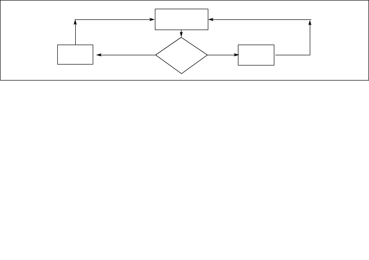
Vol. 3A 8-33
ADVANCED PROGRAMMABLE INTERRUPT CONTROLLER (APIC)
Section 8.10, “APIC Bus Message Passing Mechanism and Protocol (P6 Family, Pentium
Processors),” describes the APIC bus arbitration protocols and bus message formats, while
Section 8.6.1, “Interrupt Command Register (ICR),” describes the INIT level de-assert IPI
message.
Note that except for the SIPI IPI (see Section 8.6.1, “Interrupt Command Register (ICR)”), all
bus messages that fail to be delivered to their specified destination or destinations are automat-
ically retried. Software should avoid situations in which IPIs are sent to disabled or nonexistent
local APICs, causing the messages to be resent repeatedly.
8.8 HANDLING INTERRUPTS
When a local APIC receives an interrupt from a local source, an interrupt message from an I/O
APIC, or and IPI, the manner in which it handles the message depends on processor implemen-
tation, as described in the following sections.
8.8.1 Interrupt Handling with the Pentium 4 and Intel Xeon
Processors
With the Pentium 4 and Intel Xeon processors, the local APIC handles the local interrupts, inter-
rupt messages, and IPIs it receives as follows:
1. It determines if it is the specified destination or not (see Figure 8-16). If it is the specified
destination, it accepts the message; if it is not, it discards the message.
2. If the local APIC determines that it is the designated destination for the interrupt and if the
interrupt request is an NMI, SMI, INIT, ExtINT, or SIPI, the interrupt is sent directly to the
processor core for handling.
3. If the local APIC determines that it is the designated destination for the interrupt but the
interrupt request is not one of the interrupts given in step 2, the local APIC sets the
appropriate bit in the IRR.
Figure 8-16. Interrupt Acceptance Flow Chart for the Local APIC (Pentium 4 and Intel
Xeon Processors)
Wait to Receive
Bus Message
Belong
to
Destination?
Discard
Message
No Accept
Message
Yes

8-34 Vol. 3A
ADVANCED PROGRAMMABLE INTERRUPT CONTROLLER (APIC)
4. When interrupts are pending in the IRR and ISR register, the local APIC dispatches them
to the processor one at a time, based on their priority and the current task and processor
priorities in the TPR and PPR (see Section 8.8.3.1, “Task and Processor Priorities”).
5. When a fixed interrupt has been dispatched to the processor core for handling, the
completion of the handler routine is indicated with an instruction in the instruction handler
code that writes to the end-of-interrupt (EOI) register in the local APIC (see Section 8.8.5,
“Signaling Interrupt Servicing Completion”). The act of writing to the EOI register causes
the local APIC to delete the interrupt from its ISR queue and (for level-triggered
interrupts) send a message on the bus indicating that the interrupt handling has been
completed. (A write to the EOI register must not be included in the handler routine for an
NMI, SMI, INIT, ExtINT, or SIPI.)
8.8.2 Interrupt Handling with the P6 Family and Pentium
Processors
With the P6 family and Pentium processors, the local APIC handles the local interrupts, interrupt
messages, and IPIs it receives as follows (see Figure 8-17).
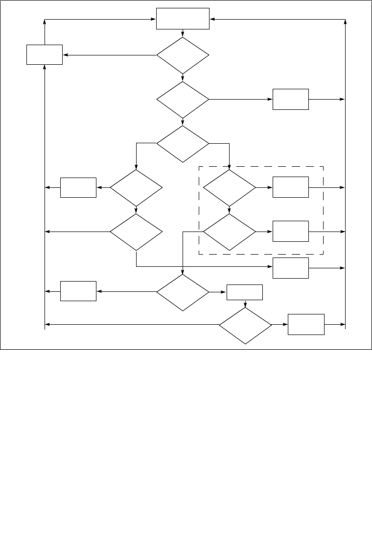
Vol. 3A 8-35
ADVANCED PROGRAMMABLE INTERRUPT CONTROLLER (APIC)
1. (IPIs only) It examines the IPI message to determines if it is the specified destination for
the IPI as described in Section 8.6.2, “Determining IPI Destination.” If it is the specified
destination, it continues its acceptance procedure; if it is not the destination, it discards the
IPI message. When the message specifies lowest-priority delivery mode, the local APIC
will arbitrate with the other processors that were designated on recipients of the IPI
message (see Section 8.6.2.4, “Lowest Priority Delivery Mode”).
2. If the local APIC determines that it is the designated destination for the interrupt and if the
interrupt request is an NMI, SMI, INIT, ExtINT, or INIT-deassert interrupt, or one of the
MP protocol IPI messages (BIPI, FIPI, and SIPI), the interrupt is sent directly to the
processor core for handling.
Figure 8-17. Interrupt Acceptance Flow Chart for the Local APIC (P6 Family and
Pentium Processors)
Wait to Receive
Bus Message
Belong
to
Destination?
Is it
NMI/SMI/INIT
/
ExtINT?
Delivery
Mode?
Am
I
Focus?
Other
Focus?
Is Interrupt
Slot Available?
Is Status
a Retry? Discard
Message
Accept
Message
Yes
Yes
Accept
Message
Is
Interrupt Slot
Available? Arbitrate
Yes
Am I
Winner? Accept
Message
Yes
No
Set Status
to Retry
No
No
Yes
Set Status
to Retry
No
Discard
Message
No
Accept
Message
Yes
Lowest
Priority
Fixed
Yes No
No
Yes
No
P6 Family
Processor Specific

8-36 Vol. 3A
ADVANCED PROGRAMMABLE INTERRUPT CONTROLLER (APIC)
3. If the local APIC determines that it is the designated destination for the interrupt but the
interrupt request is not one of the interrupts given in step 2, the local APIC looks for an
open slot in one of its two pending interrupt queues contained in the IRR and ISR registers
(see Figure 8-20). If a slot is available (see Section 8.8.4, “Interrupt Acceptance for Fixed
Interrupts”), places the interrupt in the slot. If a slot is not available, it rejects the interrupt
request and sends it back to the sender with a retry message.
4. When interrupts are pending in the IRR and ISR register, the local APIC dispatches them
to the processor one at a time, based on their priority and the current task and processor
priorities in the TPR and PPR (see Section 8.8.3.1, “Task and Processor Priorities”).
5. When a fixed interrupt has been dispatched to the processor core for handling, the
completion of the handler routine is indicated with an instruction in the instruction handler
code that writes to the end-of-interrupt (EOI) register in the local APIC (see Section 8.8.5,
“Signaling Interrupt Servicing Completion”). The act of writing to the EOI register causes
the local APIC to delete the interrupt from its queue and (for level-triggered interrupts)
send a message on the bus indicating that the interrupt handling has been completed. (A
write to the EOI register must not be included in the handler routine for an NMI, SMI,
INIT, ExtINT, or SIPI.)
The following sections describe the acceptance of interrupts and their handling by the local
APIC and processor in greater detail.
8.8.3 Interrupt, Task, and Processor Priority
For interrupts that are delivered to the processor through the local APIC, each interrupt has an
implied priority based on its vector number. The local APIC uses this priority to determine when
to service the interrupt relative to the other activities of the processor, including the servicing of
other interrupts.
For interrupt vectors in the range of 16 to 255, the interrupt priority is determined using the
following relationship:
priority = vector / 16
Here the quotient is rounded down to the nearest integer value to determine the priority, with 1
being the lowest priority and 15 is the highest. Because vectors 0 through 31 are reserved for
dedicated uses by the IA-32 architecture, the priorities of user defined interrupts range from 2
to 15.
Each interrupt priority level (sometimes interpreted by software as an interrupt priority class)
encompasses 16 vectors. Prioritizing interrupts within a priority level is determined by the
vector number. The higher the vector number, the higher the priority within that priority level.
In determining the priority of a vector and ranking of vectors within a priority group, the vector
number is often divided into two parts, with the high 4 bits of the vector indicating its priority
and the low 4 bit indicating its ranking within the priority group.

Vol. 3A 8-37
ADVANCED PROGRAMMABLE INTERRUPT CONTROLLER (APIC)
8.8.3.1 Task and Processor Priorities
The local APIC also defines a task priority and a processor priority that it uses in determining
the order in which interrupts should be handled. The task priority is a software selected value
between 0 and 15 (see Figure 8-18) that is written into the task priority register (TPR). The TPR
is a read/write register.
NOTE
In this discussion, the term “task” refers to a software defined task, process,
thread, program, or routine that is dispatched to run on the processor by the
operating system. It does not refer an IA-32 architecture defined task as
described in Chapter 6, “Task Management.”
The task priority allows software to set a priority threshold for interrupting the processor. The
processor will service only those interrupts that have a priority higher than that specified in the
TPR. If software sets the task priority in the TPR to 0, the processor will handle all interrupts; it
is it set to 15, all interrupts are inhibited from being handled, except those delivered with the
NMI, SMI, INIT, ExtINT, INIT-deassert, and start-up delivery mode. This mechanism enables
the operating system to temporarily block specific interrupts (generally low priority interrupts)
from disturbing high-priority work that the processor is doing.
Note that the task priority is also used to determine the arbitration priority of the local processor
(see Section 8.6.2.4, “Lowest Priority Delivery Mode”).
The processor priority is set by the processor, also to value between 0 and 15 (see Figure 8-19)
that is written into the processor priority register (PPR). The PPR is a read only register. The
processor priority represents the current priority at which the processor is executing. It is used
to determine whether a pending interrupt can be dispensed to the processor.
Figure 8-18. Task Priority Register (TPR)
31 078
Reserved
Address: FEE0 0080H
Value after reset: 0H
Task Priority Sub-Class
Task Priority
43

8-38 Vol. 3A
ADVANCED PROGRAMMABLE INTERRUPT CONTROLLER (APIC)
Its value in the PPR is computed as follows:
IF TPR[7:4] ≥ ISRV[7:4]
THEN
PPR[7:0] ← TPR[7:0]
ELSE
PPR[7:4] ← ISRV[7:4]
PPR[3:0] ← 0
Here, the ISRV value is the vector number of the highest priority ISR bit that is set, or 00H if no
ISR bit is set. Essentially, the processor priority is set to either to the highest priority pending
interrupt in the ISR or to the current task priority, whichever is higher.
8.8.4 Interrupt Acceptance for Fixed Interrupts
The local APIC queues the fixed interrupts that it accepts in one of two interrupt pending regis-
ters: the interrupt request register (IRR) or in-service register (ISR). These two 256-bit read-only
registers are shown in Figure 8-20. The 256 bits in these registers represent the 256 possible
vectors; vectors 0 through 15 are reserved by the APIC (see also: Section 8.5.2, “Valid Interrupt
Vectors”).
NOTE
All interrupts with an NMI, SMI, INIT, ExtINT, start-up, or INIT-deassert
delivery mode bypass the IRR and ISR registers and are sent directly to the
processor core for servicing.
Figure 8-19. Processor Priority Register (PPR)
31 078
Reserved
Address: FEE0 00A0H
Value after reset: 0H
Processor Priority Sub-Class
Processor Priority
43

Vol. 3A 8-39
ADVANCED PROGRAMMABLE INTERRUPT CONTROLLER (APIC)
The IRR contains the active interrupt requests that have been accepted, but not yet dispatched
to the processor for servicing. When the local APIC accepts an interrupt, it sets the bit in the IRR
that corresponds the vector of the accepted interrupt. When the processor core is ready to handle
the next interrupt, the local APIC clears the highest priority IRR bit that is set and sets the corre-
sponding ISR bit. The vector for the highest priority bit set in the ISR is then dispatched to the
processor core for servicing.
While the processor is servicing the highest priority interrupt, the local APIC can send additional
fixed interrupts by setting bits in the IRR. When the interrupt service routine issues a write to
the EOI register (see Section 8.8.5, “Signaling Interrupt Servicing Completion”), the local APIC
responds by clearing the highest priority ISR bit that is set. It then repeats the process of clearing
the highest priority bit in the IRR and setting the corresponding bit in the ISR. The processor
core then begins executing the service routing for the highest priority bit set in the ISR.
If more than one interrupt is generated with the same vector number, the local APIC can set the
bit for the vector both in the IRR and the ISR. This means that for the Pentium 4 and Intel Xeon
processors, the IRR and ISR can queue two interrupts for each interrupt vector: one in the IRR
and one in the ISR. Any additional interrupts issued for the same interrupt vector are collapsed
into the single bit in the IRR.
For the P6 family and Pentium processors, the IRR and ISR registers can queue no more than
two interrupts per priority level, and will reject other interrupts that are received within the same
priority level.
If the local APIC receives an interrupt with a priority higher than that of the interrupt currently
in serviced, and interrupts are enabled in the processor core, the local APIC dispatches the
higher priority interrupt to the processor immediately (without waiting for a write to the EOI
register). The currently executing interrupt handler is then interrupted so the higher-priority
interrupt can be handled. When the handling of the higher-priority interrupt has been completed,
the servicing of the interrupted interrupt is resumed.
The trigger mode register (TMR) indicates the trigger mode of the interrupt (see Figure 8-20).
Upon acceptance of an interrupt into the IRR, the corresponding TMR bit is cleared for edge-
triggered interrupts and set for level-triggered interrupts. If a TMR bit is set when an EOI cycle
for its corresponding interrupt vector is generated, an EOI message is sent to all I/O APICs.
Figure 8-20. IRR, ISR and TMR Registers
255 0
Reserved
Addresses: IRR FEE0 0200H - FEE0 0270H
Value after reset: 0H
16 15
IRR
Reserved ISR
Reserved TMR
ISR FEE0 0100H - FEE0 0170H
TMR FEE0 0180H - FEE0 01F0H

8-40 Vol. 3A
ADVANCED PROGRAMMABLE INTERRUPT CONTROLLER (APIC)
8.8.5 Signaling Interrupt Servicing Completion
For all interrupts except those delivered with the NMI, SMI, INIT, ExtINT, the start-up, or INIT-
Deassert delivery mode, the interrupt handler must include a write to the end-of-interrupt (EOI)
register (see Figure 8-21). This write must occur at the end of the handler routine, sometime
before the IRET instruction. This action indicates that the servicing of the current interrupt is
complete and the local APIC can issue the next interrupt from the ISR.
Upon receiving and EOI, the APIC clears the highest priority bit in the ISR and dispatches the
next highest priority interrupt to the processor. If the terminated interrupt was a level-triggered
interrupt, the local APIC also sends an end-of-interrupt message to all I/O APICs.
For future compatibility, the software is requested to issue the end-of-interrupt command by
writing a value of 0H into the EOI register.
8.8.6 Task Priority in IA-32e Mode
In IA-32e mode, operating systems can manage the 16 priority classes of external interrupts (see
Section 8.8.3, “Interrupt, Task, and Processor Priority”) explicitly using the task priority register
(TPR). Operating systems can use the TPR to temporarily block specific (low-priority) inter-
rupts from interrupting a high-priority task. This is done by loading TPR with a value corre-
sponding to the highest-priority interrupt that is to be blocked. For example:
•Loading TPR with a value of 8(01000B) blocks all interrupts with a priority of 8 or less
while allowing all interrupts with a priority of nine or more to be recognized.
•Loading the TPR with zero enables all external interrupts.
•Loading TPR with 0 (01111B) disables all external interrupts.
The TPR (shown in Figure 8-18) is cleared to 0 on reset. In 64-bit mode, software can read and
write the TPR using an alternate interface, MOV CR8 instruction. The new priority level is
established when the MOV CR8 instruction completes execution. Software does not need to
force serialization after loading the TPR using MOV CR8.
Use of the MOV CRn instruction requires a privilege level of 0. Programs running at privilege
level greater than 0 cannot read or write the TPR. An attempt to do so results in a general-protec-
tion exception, #GP(0). The TPR is abstracted from the interrupt controller (IC), which priori-
tizes and manages external interrupt delivery to the processor. The IC can be an external device,
such as an APIC or 8259. Typically, the IC provides a priority mechanism similar or identical to
Figure 8-21. EOI Register
31 0
Address: 0FEE0 00B0H
Value after reset: 0H

Vol. 3A 8-41
ADVANCED PROGRAMMABLE INTERRUPT CONTROLLER (APIC)
the TPR. The IC, however, is considered implementation-dependent with the under-lying
priority mechanisms subject to change. The CR8, by contrast, is part of the Intel EM64T archi-
tecture. Software can depend on this definition remaining unchanged.
Figure 8-22 shows the layout of CR8; only the low four bits are used. The remaining 60 bits are
reserved and must be written with zeros. Failure to do this results in a general-protection excep-
tion, #GP(0).
8.8.6.1 Interaction of Task Priorities between CR8 and APIC
The first implementation of Intel EM64T includes a local advanced programmable interrupt
controller (APIC) that is similar to the APIC used with previous IA-32 processors. Some aspects
of the local APIC affect the operation of the architecturally defined task priority register and the
programming interface using CR8.
Notable CR8 and APIC interactions are:
•The processor powers up with the local APIC enabled.
•The APIC must be enabled for CR8 to function as the TPR. Writes to CR8 are reflected
into the APIC Task Priority Register.
•APIC.TPR[bits 7:4] = CR8[bits 3:0], APIC.TPR[bits 3:0] = 0. A read of CR8 returns a
64-bit value which is the value of TPR[bits 7:4], zero extended to 64 bits.
There are no ordering mechanisms between direct updates of the APIC.TPR and CR8. Operating
software should implement either direct APIC TPR updates or CR8 style TPR updates but not
mix them. Software can use a serializing instruction (for example, CPUID) to serialize updates
between MOV CR8 and stores to the APIC.
8.9 SPURIOUS INTERRUPT
A special situation may occur when a processor raises its task priority to be greater than or equal
to the level of the interrupt for which the processor INTR signal is currently being asserted. If
at the time the INTA cycle is issued, the interrupt that was to be dispensed has become masked
(programmed by software), the local APIC will deliver a spurious-interrupt vector. Dispensing
the spurious-interrupt vector does not affect the ISR, so the handler for this vector should return
without an EOI.
Figure 8-22. CR8 Register
63 0
Value after reset: 0H
34
Reserved
8-42 Vol. 3A
ADVANCED PROGRAMMABLE INTERRUPT CONTROLLER (APIC)
The vector number for the spurious-interrupt vector is specified in the spurious-interrupt vector
register (see Figure 8-23). The functions of the fields in this register are as follows:
Spurious Vector Determines the vector number to be delivered to the processor when
the local APIC generates a spurious vector.
(Pentium 4 and Intel Xeon processors.) Bits 0 through 7 of the this
field are programmable by software.
(P6 family and Pentium processors). Bits 4 through 7 of the this field
are programmable by software, and bits 0 through 3 are hardwired to
logical ones. Software writes to bits 0 through 3 have no effect.
APIC Software Allows software to temporarily enable (1) or disable (0) the local
Enable/Disable APIC (see Section 8.4.3, “Enabling or Disabling the Local APIC”).
Focus Processor Determines if focus processor checking is enabled (0) or disabled (1)
Checking when using the lowest-priority delivery mode. In Pentium 4 and Intel
Xeon processors, this bit is reserved and should be cleared to 0.
NOTE
Do not program an LVT or IOAPIC RTE with a spurious vector even if you
set the mask bit. A spurious vector ISR does not do an EOI. If for some
reason an interrupt is generated by an LVT or RTE entry, the bit in the in-
service register will be left set for the spurious vector. This will mask all
interrrupts at the same or lower priority
Figure 8-23. Spurious-Interrupt Vector Register (SVR)
31 0
Reserved
7
Focus Processor Checking1
APIC Software Enable/Disable
8910
0: APIC Disabled
1: APIC Enabled
Spurious Vector2
Address: FEE0 00F0H
Value after reset: 0000 00FFH
0: Enabled
1: Disabled
2. For the P6 family and Pentium processors, bits 0 through 3
of the spurious vector are hardwired to 1.
1. Not supported in Pentium 4 and Intel Xeon processors.

Vol. 3A 8-43
ADVANCED PROGRAMMABLE INTERRUPT CONTROLLER (APIC)
8.10 APIC BUS MESSAGE PASSING MECHANISM AND
PROTOCOL (P6 FAMILY, PENTIUM PROCESSORS)
The Pentium 4 and Intel Xeon processors pass messages among the local and I/O APICs on the
system bus, using the system bus message passing mechanism and protocol.
The P6 family and Pentium processors, pass messages among the local and I/O APICs on the
serial APIC bus, as follows. Because only one message can be sent at a time on the APIC bus,
the I/O APIC and local APICs employ a “rotating priority” arbitration protocol to gain permis-
sion to send a message on the APIC bus. One or more APICs may start sending their messages
simultaneously. At the beginning of every message, each APIC presents the type of the message
it is sending and its current arbitration priority on the APIC bus. This information is used for
arbitration. After each arbitration cycle (within an arbitration round), only the potential winners
keep driving the bus. By the time all arbitration cycles are completed, there will be only one
APIC left driving the bus. Once a winner is selected, it is granted exclusive use of the bus, and
will continue driving the bus to send its actual message.
After each successfully transmitted message, all APICs increase their arbitration priority by 1.
The previous winner (that is, the one that has just successfully transmitted its message) assumes
a priority of 0 (lowest). An agent whose arbitration priority was 15 (highest) during arbitration,
but did not send a message, adopts the previous winner’s arbitration priority, increments by 1.
Note that the arbitration protocol described above is slightly different if one of the APICs issues
a special End-Of-Interrupt (EOI). This high-priority message is granted the bus regardless of its
sender’s arbitration priority, unless more than one APIC issues an EOI message simultaneously.
In the latter case, the APICs sending the EOI messages arbitrate using their arbitration priorities.
If the APICs are set up to use “lowest priority” arbitration (see Section 8.6.2.4, “Lowest Priority
Delivery Mode”) and multiple APICs are currently executing at the lowest priority (the value in
the APR register), the arbitration priorities (unique values in the Arb ID register) are used to
break ties. All 8 bits of the APR are used for the lowest priority arbitration.
8.10.1 Bus Message Formats
See Appendix F, “APIC Bus Message Formats,” for a description of bus message formats used
to transmit messages on the serial APIC bus.
8.11 MESSAGE SIGNALLED INTERRUPTS
The PCI Local Bus Specification, Rev 2.2 (www.pcisig.com) introduces the concept of message
signalled interrupts. Intel processors and chipsets with this capability currently include the
Pentium 4 and Intel Xeon processors. As the specification indicates:
“Message signalled interrupts (MSI) is an optional feature that enables PCI
devices to request service by writing a system-specified message to a system-
specified address (PCI DWORD memory write transaction). The transaction
address specifies the message destination while the transaction data specifies
the message. System software is expected to initialize the message

8-44 Vol. 3A
ADVANCED PROGRAMMABLE INTERRUPT CONTROLLER (APIC)
destination and message during device configuration, allocating one or more
non-shared messages to each MSI capable function.”
The capabilities mechanism provided by the PCI Local Bus Specification is used to identify and
configure MSI capable PCI devices. Among other fields, this structure contains a Message Data
Register and a Message Address Register. To request service, the PCI device function writes the
contents of the Message Data Register to the address contained in the Message Address Register
(and the Message Upper Address register for 64-bit message addresses).
Section 8.11.1 and Section 8.11.2 provide layout details for the Message Address Register and
the Message Data Register. The operation issued by the device is a PCI write command to the
Message Address Register with the Message Data Register contents. The operation follows
semantic rules as defined for PCI write operations and is a DWORD operation.
8.11.1 Message Address Register Format
The format of the Message Address Register (lower 32-bits) is shown in Figure 8-24.
Fields in the Message Address Register are as follows:
1. Bits 31-20 — These bits contain a fixed value for interrupt messages (0FEEH). This value
locates interrupts at the 1-MByte area with a base address of 4G – 18M. All accesses to this
region are directed as interrupt messages. Care must to be taken to ensure that no other
device claims the region as I/O space.
2. Destination ID — This field contains an 8-bit destination ID. It identifies the message’s
target processor(s). The destination ID corresponds to bits 63:56 of the I/O APIC
Redirection Table Entry if the IOAPIC is used to dispatch the interrupt to the processor(s).
3. Redirection hint indication (RH) — This bit indicates whether the message should be
directed to the processor with the lowest interrupt priority among processors that can
receive the interrupt.
•When RH is 0, the interrupt is directed to the processor listed in the Destination ID
field.
•When RH is 1 and the physical destination mode is used, the Destination ID field
must not be set to 0xFF; it must point to a processor that is present and enabled to
receive the interrupt.
Figure 8-24. Layout of the MSI Message Address Register
31 20 19 12 11 4 3 2 1 0
0FEEH Destination ID Reserved RH DM XX

Vol. 3A 8-45
ADVANCED PROGRAMMABLE INTERRUPT CONTROLLER (APIC)
•When RH is 1 and the logical destination mode is active in a system using a flat
addressing model, the Destination ID field must be set so that bits set to 1 identify
processors that are present and enabled to receive the interrupt.
•If RH is set to 1 and the logical destination mode is active in a system using cluster
addressing model, then Destination ID field must not be set to 0xFF; the
processors identified with this field must be present and enabled to receive the
interrupt.
4. Destination mode (DM) — This bit indicates whether the Destination ID field should be
interpreted as logical or physical APIC ID for delivery of the lowest priority interrupt. If
RH is 1 and DM is 0, the Destination ID field is in physical destination mode and only the
processor in the system that has the matching APIC ID is considered for delivery of that
interrupt (this means no re-direction). If RH is 1 and DM is 1, the Destination ID Field is
interpreted as in logical destination mode and the redirection is limited to only those
processors that are part of the logical group of processors based on the processor’s logical
APIC ID and the Destination ID field in the message. The logical group of processors
consists of those identified by matching the 8-bit Destination ID with the logical
destination identified by the Destination Format Register and the Logical Destination
Register in each local APIC. The details are similar to those described in Section 8.6.2,
“Determining IPI Destination.” If RH is 0, then the DM bit is ignored and the message is
sent ahead independent of whether the physical or logical destination mode is used.
8.11.2 Message Data Register Format
The layout of the Message Data Register is shown in Figure 8-25.
8-46 Vol. 3A
ADVANCED PROGRAMMABLE INTERRUPT CONTROLLER (APIC)
Reserved fields are not assumed to be any value. Software must preserve their contents on
writes. Other fields in the Message Data Register are described below.
1. Vector — This 8-bit field contains the interrupt vector associated with the message. Values
range from 010H to 0FEH. Software must guarantee that the field is not programmed with
vector 00H to 0FH.
2. Delivery Mode — This 3-bit field specifies how the interrupt receipt is handled. Delivery
Modes operate only in conjunction with specified Trigger Modes. Correct Trigger Modes
must be guaranteed by software. Restrictions are indicated below:
a. 000B (Fixed Mode) — Deliver the signal to all the agents listed in the destination.
The Trigger Mode for fixed delivery mode can be edge or level.
b. 001B (Lowest Priority) — Deliver the signal to the agent that is executing at the
lowest priority of all agents listed in the destination field. The trigger mode can be
edge or level.
c. 010B (System Management Interrupt or SMI) — The delivery mode is edge only.
For systems that rely on SMI semantics, the vector field is ignored but must be
programmed to all zeroes for future compatibility.
Figure 8-25. Layout of the MSI Message Data Register
Reserved
Reserved Reserved Vector
Delivery Mode
001 - Lowest Priority
010 - SMI
011 - Reserved
101 - INIT
110 - Reserved
111 - ExtINT
Trigger Mode
0 - Edge
1 - Level
Level for Trigger Mode = 0
X - Don’t care
Level for Trigger Mode = 1
0 - Deassert
1 - Assert
000 - Fixed
001 - NMI
31 16 15 14 13 11 10 8 7 0
63 32

Vol. 3A 8-47
ADVANCED PROGRAMMABLE INTERRUPT CONTROLLER (APIC)
d. 100B (NMI) — Deliver the signal to all the agents listed in the destination field. The
vector information is ignored. NMI is an edge triggered interrupt regardless of the
Trigger Mode Setting.
e. 101B (INIT) — Deliver this signal to all the agents listed in the destination field. The
vector information is ignored. INIT is an edge triggered interrupt regardless of the
Trigger Mode Setting.
f. 111B (ExtINT) — Deliver the signal to the INTR signal of all agents in the destination
field (as an interrupt that originated from an 8259A compatible interrupt controller).
The vector is supplied by the INTA cycle issued by the activation of the ExtINT.
ExtINT is an edge triggered interrupt.
3. Level — Edge triggered interrupt messages are always interpreted as assert messages. For
edge triggered interrupts this field is not used. For level triggered interrupts, this bit
reflects the state of the interrupt input.
4. Trigger Mode — This field indicates the signal type that will trigger a message.
a. 0 — Indicates edge sensitive.
b. 1 — Indicates level sensitive.

8-48 Vol. 3A
ADVANCED PROGRAMMABLE INTERRUPT CONTROLLER (APIC)

9
Processor
Management and
Initialization

Vol. 3A 9-1
CHAPTER 9
PROCESSOR MANAGEMENT AND
INITIALIZATION
This chapter describes the facilities provided for managing processor wide functions and for
initializing the processor. The subjects covered include: processor initialization, x87 FPU
initialization, processor configuration, feature determination, mode switching, the MSRs (in the
Pentium, P6 family, Pentium 4, and Intel Xeon processors), and the MTRRs (in the P6 family,
Pentium 4, and Intel Xeon processors).
9.1 INITIALIZATION OVERVIEW
Following power-up or an assertion of the RESET# pin, each processor on the system bus
performs a hardware initialization of the processor (known as a hardware reset) and an optional
built-in self-test (BIST). A hardware reset sets each processor’s registers to a known state and
places the processor in real-address mode. It also invalidates the internal caches, translation
lookaside buffers (TLBs) and the branch target buffer (BTB). At this point, the action taken
depends on the processor family:
•Pentium 4 and Intel Xeon processors — All the processors on the system bus (including
a single processor in a uniprocessor system) execute the multiple processor (MP) initial-
ization protocol. The processor that is selected through this protocol as the bootstrap
processor (BSP) then immediately starts executing software-initialization code in the
current code segment beginning at the offset in the EIP register. The application (non-BSP)
processors (APs) go into a Wait For Startup IPI (SIPI) state while the BSP is executing
initialization code. See Section 7.5, “Multiple-Processor (MP) Initialization,” for more
details. Note that in a uniprocessor system, the single Pentium 4 or Intel Xeon processor
automatically becomes the BSP.
•P6 family processors — The action taken is the same as for the Pentium 4 and Intel Xeon
processors (as described in the previous paragraph).
•Pentium processors — In either a single- or dual- processor system, a single Pentium
processor is always pre-designated as the primary processor. Following a reset, the primary
processor behaves as follows in both single- and dual-processor systems. Using the dual-
processor (DP) ready initialization protocol, the primary processor immediately starts
executing software-initialization code in the current code segment beginning at the offset
in the EIP register. The secondary processor (if there is one) goes into a halt state.
•Intel486 processor — The primary processor (or single processor in a uniprocessor
system) immediately starts executing software-initialization code in the current code
segment beginning at the offset in the EIP register. (The Intel486 does not automatically
execute a DP or MP initialization protocol to determine which processor is the primary
processor.)

9-2 Vol. 3A
PROCESSOR MANAGEMENT AND INITIALIZATION
The software-initialization code performs all system-specific initialization of the BSP or
primary processor and the system logic.
At this point, for MP (or DP) systems, the BSP (or primary) processor wakes up each AP (or
secondary) processor to enable those processors to execute self-configuration code.
When all processors are initialized, configured, and synchronized, the BSP or primary processor
begins executing an initial operating-system or executive task.
The x87 FPU is also initialized to a known state during hardware reset. x87 FPU software initial-
ization code can then be executed to perform operations such as setting the precision of the x87
FPU and the exception masks. No special initialization of the x87 FPU is required to switch
operating modes.
Asserting the INIT# pin on the processor invokes a similar response to a hardware reset. The
major difference is that during an INIT, the internal caches, MSRs, MTRRs, and x87 FPU state
are left unchanged (although, the TLBs and BTB are invalidated as with a hardware reset). An
INIT provides a method for switching from protected to real-address mode while maintaining
the contents of the internal caches.
9.1.1 Processor State After Reset
Table 9-1 shows the state of the flags and other registers following power-up for the Pentium 4,
Intel Xeon, P6 family, and Pentium processors. The state of control register CR0 is 60000010H
(see Figure 9-1). This places the processor is in real-address mode with paging disabled.
9.1.2 Processor Built-In Self-Test (BIST)
Hardware may request that the BIST be performed at power-up. The EAX register is cleared
(0H) if the processor passes the BIST. A nonzero value in the EAX register after the BIST indi-
cates that a processor fault was detected. If the BIST is not requested, the contents of the EAX
register after a hardware reset is 0H.
The overhead for performing a BIST varies between processor families. For example, the BIST
takes approximately 30 million processor clock periods to execute on the Pentium 4 processor.
(This clock count is model-specific, and Intel reserves the right to change the exact number of
periods, for any of the IA-32 processors, without notification.)

Vol. 3A 9-3
PROCESSOR MANAGEMENT AND INITIALIZATION
Table 9-1. IA-32 Processor States Following Power-up, Reset, or INIT
Register Pentium 4 and Intel Xeon
Processor P6 Family Processor Pentium Processor
EFLAGS100000002H 00000002H 00000002H
EIP 0000FFF0H 0000FFF0H 0000FFF0H
CR0 60000010H260000010H260000010H2
CR2, CR3, CR4 00000000H 00000000H 00000000H
CS Selector = F000H
Base = FFFF0000H
Limit = FFFFH
AR = Present, R/W,
Accessed
Selector = F000H
Base = FFFF0000H
Limit = FFFFH
AR = Present, R/W,
Accessed
Selector = F000H
Base = FFFF0000H
Limit = FFFFH
AR = Present, R/W,
Accessed
SS, DS, ES, FS,
GS Selector = 0000H
Base = 00000000H
Limit = FFFFH
AR = Present, R/W,
Accessed
Selector = 0000H
Base = 00000000H
Limit = FFFFH
AR = Present, R/W,
Accessed
Selector = 0000H
Base = 00000000H
Limit = FFFFH
AR = Present, R/W,
Accessed
EDX 00000FxxH 000n06xxH3 000005xxH
EAX 040404
EBX, ECX, ESI,
EDI, EBP, ESP 00000000H 00000000H 00000000H
ST0 through
ST75Pwr up or Reset: +0.0
FINIT/FNINIT: Unchanged Pwr up or Reset: +0.0
FINIT/FNINIT: Unchanged Pwr up or Reset: +0.0
FINIT/FNINIT: Unchanged
x87 FPU Control
Word5Pwr up or Reset: 0040H
FINIT/FNINIT: 037FH Pwr up or Reset: 0040H
FINIT/FNINIT: 037FH Pwr up or Reset: 0040H
FINIT/FNINIT: 037FH
x87 FPU Status
Word5Pwr up or Reset: 0000H
FINIT/FNINIT: 0000H Pwr up or Reset: 0000H
FINIT/FNINIT: 0000H Pwr up or Reset: 0000H
FINIT/FNINIT: 0000H
x87 FPU Tag
Word5Pwr up or Reset: 5555H
FINIT/FNINIT: FFFFH Pwr up or Reset: 5555H
FINIT/FNINIT: FFFFH Pwr up or Reset: 5555H
FINIT/FNINIT: FFFFH
x87 FPU Data
Operand and CS
Seg. Selectors5
Pwr up or Reset: 0000H
FINIT/FNINIT: 0000H Pwr up or Reset: 0000H
FINIT/FNINIT: 0000H Pwr up or Reset: 0000H
FINIT/FNINIT: 0000H
x87 FPU Data
Operand and
Inst. Pointers5
Pwr up or Reset:
00000000H
FINIT/FNINIT: 00000000H
Pwr up or Reset:
00000000H
FINIT/FNINIT: 00000000H
Pwr up or Reset:
00000000H
FINIT/FNINIT:
00000000H
MM0 through
MM75Pwr up or Reset:
0000000000000000H
INIT or FINIT/FNINIT:
Unchanged
Pentium II and Pentium III
Processors Only—
Pwr up or Reset:
0000000000000000H
INIT or FINIT/FNINIT:
Unchanged
Pentium with MMX
Technology Only—
Pwr up or Reset:
0000000000000000H
INIT or FINIT/FNINIT:
Unchanged
XMM0 through
XMM7 Pwr up or Reset:
0000000000000000H
INIT: Unchanged
Pentium III processor
Only—
Pwr up or Reset:
0000000000000000H
INIT: Unchanged
NA

9-4 Vol. 3A
PROCESSOR MANAGEMENT AND INITIALIZATION
MXCSR Pwr up or Reset: 1F80H
INIT: Unchanged Pentium III processor only-
Pwr up or Reset: 1F80H
INIT: Unchanged
NA
GDTR, IDTR Base = 00000000H
Limit = FFFFH
AR = Present, R/W
Base = 00000000H
Limit = FFFFH
AR = Present, R/W
Base = 00000000H
Limit = FFFFH
AR = Present, R/W
LDTR, Task
Register Selector = 0000H
Base = 00000000H
Limit = FFFFH
AR = Present, R/W
Selector = 0000H
Base = 00000000H
Limit = FFFFH
AR = Present, R/W
Selector = 0000H
Base = 00000000H
Limit = FFFFH
AR = Present, R/W
DR0, DR1, DR2,
DR3 00000000H 00000000H 00000000H
DR6 FFFF0FF0H FFFF0FF0H FFFF0FF0H
DR7 00000400H 00000400H 00000400H
Time-Stamp
Counter Power up or Reset: 0H
INIT: Unchanged Power up or Reset: 0H
INIT: Unchanged Power up or Reset: 0H
INIT: Unchanged
Perf. Counters
and Event Select Power up or Reset: 0H
INIT: Unchanged Power up or Reset: 0H
INIT: Unchanged Power up or Reset: 0H
INIT: Unchanged
All Other MSRs Pwr up or Reset:
Undefined
INIT: Unchanged
Pwr up or Reset:
Undefined
INIT: Unchanged
Pwr up or Reset:
Undefined
INIT: Unchanged
Data and Code
Cache, TLBs Invalid Invalid Invalid
Fixed MTRRs Pwr up or Reset: Disabled
INIT: Unchanged Pwr up or Reset: Disabled
INIT: Unchanged Not Implemented
Variable MTRRs Pwr up or Reset: Disabled
INIT: Unchanged Pwr up or Reset: Disabled
INIT: Unchanged Not Implemented
Machine-Check
Architecture Pwr up or Reset:
Undefined
INIT: Unchanged
Pwr up or Reset:
Undefined
INIT: Unchanged
Not Implemented
APIC Pwr up or Reset: Enabled
INIT: Unchanged Pwr up or Reset: Enabled
INIT: Unchanged Pwr up or Reset: Enabled
INIT: Unchanged
NOTES:
1. The 10 most-significant bits of the EFLAGS register are undefined following a reset. Software should
not depend on the states of any of these bits.
2. The CD and NW flags are unchanged, bit 4 is set to 1, all other bits are cleared.
3. Where “n” is the Extended Model Value for the respective processor.
4. If Built-In Self-Test (BIST) is invoked on power up or reset, EAX is 0 only if all tests passed. (BIST can-
not be invoked during an INIT.)
5. The state of the x87 FPU and MMX registers is not changed by the execution of an INIT.
Table 9-1. IA-32 Processor States Following Power-up, Reset, or INIT (Contd.)
Register Pentium 4 and Intel Xeon
Processor P6 Family Processor Pentium Processor
Vol. 3A 9-5
PROCESSOR MANAGEMENT AND INITIALIZATION
9.1.3 Model and Stepping Information
Following a hardware reset, the EDX register contains component identification and revision
information (see Figure 9-2). For example, the model, family, and processor type returned for
the first processor in the Intel Pentium 4 family is as follows: model (0000B), family (1111B),
and processor type (00B).
The stepping ID field contains a unique identifier for the processor’s stepping ID or revision
level. The extended family and extended model fields were added to the IA-32 architecture in
the Pentium 4 processors.
Figure 9-1. Contents of CR0 Register after Reset
Figure 9-2. Version Information in the EDX Register after Reset
External x87 FPU error reporting: 0
(Not used): 1
No task switch: 0
x87 FPU instructions not trapped: 0
WAIT/FWAIT instructions not trapped: 0
Real-address mode: 0
31 19 16 15 0
P
E
123456
1718
282930
M
P
E
M
1
N
ET
S
P
GC
DN
WW
P
A
M
Paging disabled: 0
Alignment check disabled: 0
Caching disabled: 1
Not write-through disabled: 1
Write-protect disabled: 0
Reserved Reserved
31 12 11 8 7 4 3 0
EAX
Family (1111B for the Pentium 4 Processor Family)
Model (Beginning with 0000B)
1314
Processor Type
Model
Family Stepping
ID
15
Model
Extended
Extended
Family
1619202324
Reserved

9-6 Vol. 3A
PROCESSOR MANAGEMENT AND INITIALIZATION
9.1.4 First Instruction Executed
The first instruction that is fetched and executed following a hardware reset is located at physical
address FFFFFFF0H. This address is 16 bytes below the processor’s uppermost physical
address. The EPROM containing the software-initialization code must be located at this address.
The address FFFFFFF0H is beyond the 1-MByte addressable range of the processor while in
real-address mode. The processor is initialized to this starting address as follows. The CS
register has two parts: the visible segment selector part and the hidden base address part. In real-
address mode, the base address is normally formed by shifting the 16-bit segment selector value
4 bits to the left to produce a 20-bit base address. However, during a hardware reset, the segment
selector in the CS register is loaded with F000H and the base address is loaded with
FFFF0000H. The starting address is thus formed by adding the base address to the value in the
EIP register (that is, FFFF0000 + FFF0H = FFFFFFF0H).
The first time the CS register is loaded with a new value after a hardware reset, the processor
will follow the normal rule for address translation in real-address mode (that is, [CS base
address = CS segment selector * 16]). To insure that the base address in the CS register remains
unchanged until the EPROM based software-initialization code is completed, the code must not
contain a far jump or far call or allow an interrupt to occur (which would cause the CS selector
value to be changed).
9.2 X87 FPU INITIALIZATION
Software-initialization code can determine the whether the processor contains an x87 FPU by
using the CPUID instruction. The code must then initialize the x87 FPU and set flags in control
register CR0 to reflect the state of the x87 FPU environment.
A hardware reset places the x87 FPU in the state shown in Table 9-1. This state is different from
the state the x87 FPU is placed in following the execution of an FINIT or FNINIT instruction
(also shown in Table 9-1). If the x87 FPU is to be used, the software-initialization code should
execute an FINIT/FNINIT instruction following a hardware reset. These instructions, tag all
data registers as empty, clear all the exception masks, set the TOP-of-stack value to 0, and select
the default rounding and precision controls setting (round to nearest and 64-bit precision).
If the processor is reset by asserting the INIT# pin, the x87 FPU state is not changed.
9.2.1 Configuring the x87 FPU Environment
Initialization code must load the appropriate values into the MP, EM, and NE flags of control
register CR0. These bits are cleared on hardware reset of the processor. Figure 9-2 shows the
suggested settings for these flags, depending on the IA-32 processor being initialized. Initializa-
tion code can test for the type of processor present before setting or clearing these flags.

Vol. 3A 9-7
PROCESSOR MANAGEMENT AND INITIALIZATION
The EM flag determines whether floating-point instructions are executed by the x87 FPU (EM
is cleared) or a device-not-available exception (#NM) is generated for all floating-point instruc-
tions so that an exception handler can emulate the floating-point operation (EM = 1). Ordinarily,
the EM flag is cleared when an x87 FPU or math coprocessor is present and set if they are not
present. If the EM flag is set and no x87 FPU, math coprocessor, or floating-point emulator is
present, the processor will hang when a floating-point instruction is executed.
The MP flag determines whether WAIT/FWAIT instructions react to the setting of the TS flag.
If the MP flag is clear, WAIT/FWAIT instructions ignore the setting of the TS flag; if the MP
flag is set, they will generate a device-not-available exception (#NM) if the TS flag is set. Gener-
ally, the MP flag should be set for processors with an integrated x87 FPU and clear for proces-
sors without an integrated x87 FPU and without a math coprocessor present. However, an
operating system can choose to save the floating-point context at every context switch, in which
case there would be no need to set the MP bit.
Table 2-1 shows the actions taken for floating-point and WAIT/FWAIT instructions based on the
settings of the EM, MP, and TS flags.
The NE flag determines whether unmasked floating-point exceptions are handled by generating
a floating-point error exception internally (NE is set, native mode) or through an external inter-
rupt (NE is cleared). In systems where an external interrupt controller is used to invoke numeric
exception handlers (such as MS-DOS-based systems), the NE bit should be cleared.
9.2.2 Setting the Processor for x87 FPU Software Emulation
Setting the EM flag causes the processor to generate a device-not-available exception (#NM)
and trap to a software exception handler whenever it encounters a floating-point instruction.
(Table 9-2 shows when it is appropriate to use this flag.) Setting this flag has two functions:
•It allows x87 FPU code to run on an IA-32 processor that has neither an integrated x87
FPU nor is connected to an external math coprocessor, by using a floating-point emulator.
•It allows floating-point code to be executed using a special or nonstandard floating-point
emulator, selected for a particular application, regardless of whether an x87 FPU or math
coprocessor is present.
Table 9-2. Recommended Settings of EM and MP Flags on IA-32 Processors
EM MP NE IA-32 processor
1 0 1 Intel486™ SX, Intel386™ DX, and Intel386™ SX processors
only, without the presence of a math coprocessor.
0 1 1 or 0*Pentium 4, Intel Xeon, P6 family, Pentium, Intel486™ DX, and
Intel 487 SX processors, and Intel386 DX and Intel386 SX
processors when a companion math coprocessor is present.
NOTE:
* The setting of the NE flag depends on the operating system being used.

9-8 Vol. 3A
PROCESSOR MANAGEMENT AND INITIALIZATION
To emulate floating-point instructions, the EM, MP, and NE flag in control register CR0 should
be set as shown in Table 9-3.
Regardless of the value of the EM bit, the Intel486 SX processor generates a device-not-avail-
able exception (#NM) upon encountering any floating-point instruction.
9.3 CACHE ENABLING
The IA-32 processors (beginning with the Intel486 processor) contain internal instruction and
data caches. These caches are enabled by clearing the CD and NW flags in control register CR0.
(They are set during a hardware reset.) Because all internal cache lines are invalid following
reset initialization, it is not necessary to invalidate the cache before enabling caching. Any
external caches may require initialization and invalidation using a system-specific initialization
and invalidation code sequence.
Depending on the hardware and operating system or executive requirements, additional config-
uration of the processor’s caching facilities will probably be required. Beginning with the
Intel486 processor, page-level caching can be controlled with the PCD and PWT flags in page-
directory and page-table entries. Beginning with the P6 family processors, the memory type
range registers (MTRRs) control the caching characteristics of the regions of physical memory.
(For the Intel486 and Pentium processors, external hardware can be used to control the caching
characteristics of regions of physical memory.) See Chapter 10, “Memory Cache Control,” for
detailed information on configuration of the caching facilities in the Pentium 4, Intel Xeon, and
P6 family processors and system memory.
Table 9-3. Software Emulation Settings of EM, MP, and NE Flags
CR0 Bit Value
EM 1
MP 0
NE 1

Vol. 3A 9-9
PROCESSOR MANAGEMENT AND INITIALIZATION
9.4 MODEL-SPECIFIC REGISTERS (MSRS)
The Pentium 4, Intel Xeon, P6 family, and Pentium processors contain a model-specific registers
(MSRs). These registers are by definition implementation specific; that is, they are not guaran-
teed to be supported on future IA-32 processors and/or to have the same functions. The MSRs
are provided to control a variety of hardware- and software-related features, including:
•The performance-monitoring counters (see Section 18.10, “Performance Monitoring
Overview”).
•(Pentium 4, Intel Xeon, and P6 family processors only.) Debug extensions (see Section
18.4, “Last Branch Recording Overview”).
•(Pentium 4, Intel Xeon, and P6 family processors only.) The machine-check exception
capability and its accompanying machine-check architecture (see Chapter 14, “Machine-
Check Architecture”).
•(Pentium 4, Intel Xeon, and P6 family processors only.) The MTRRs (see Section 10.11,
“Memory Type Range Registers (MTRRs)”).
The MSRs can be read and written to using the RDMSR and WRMSR instructions, respectively.
When performing software initialization of a Pentium 4, Intel Xeon, P6 family, or Pentium
processor, many of the MSRs will need to be initialized to set up things like performance-moni-
toring events, run-time machine checks, and memory types for physical memory.
The list of available performance-monitoring counters for the Pentium 4, Intel Xeon, P6 family,
and Pentium processors is given in Appendix A, “Performance-Monitoring Events,” and the list
of available MSRs for the Pentium 4, Intel Xeon, P6 family, and Pentium processors is given in
Appendix B, “Model-Specific Registers (MSRs).” The references earlier in this section show
where the functions of the various groups of MSRs are described in this manual.
9.5 MEMORY TYPE RANGE REGISTERS (MTRRS)
Memory type range registers (MTRRs) were introduced into the IA-32 architecture with the
Pentium Pro processor. They allow the type of caching (or no caching) to be specified in system
memory for selected physical address ranges. They allow memory accesses to be optimized for
various types of memory such as RAM, ROM, frame buffer memory, and memory-mapped I/O
devices.
In general, initializing the MTRRs is normally handled by the software initialization code or
BIOS and is not an operating system or executive function. At the very least, all the MTRRs
must be cleared to 0, which selects the uncached (UC) memory type. See Section 10.11,
“Memory Type Range Registers (MTRRs),” for detailed information on the MTRRs.

9-10 Vol. 3A
PROCESSOR MANAGEMENT AND INITIALIZATION
9.6 INITIALIZING SSE/SSE2/SSE3 EXTENSIONS
For processors that contain SSE/SSE2/SSE3 extensions, steps must be taken when initializing
the processor to allow execution of these instructions.
1. Check the CPUID feature flags for the presence of the SSE/SSE2/SSE3 extensions
(respectively: EDX bits 25 and 26, ECX bit 0) and support for the FXSAVE and
FXRSTOR instructions (EDX bit 24). Also check for support for the CLFLUSH
instruction (EDX bit 19). The CPUID feature flags are loaded in the EDX and ECX
registers when the CPUID instruction is executed with a 1 in the EAX register.
2. Set the OSFXSR flag (bit 9 in control register CR4) to indicate that the operating system
supports saving and restoring the SSE/SSE2/SSE3 execution environment (XXM and
MXCSR registers) with the FXSAVE and FXRSTOR instructions, respectively. See
Section 2.5, “Control Registers,” for a description of the OSFXSR flag.
3. Set the OSXMMEXCPT flag (bit 10 in control register CR4) to indicate that the operating
system supports the handling of SSE/SSE2/SSE3 SIMD floating-point exceptions (#XF).
See Section 2.5, “Control Registers,” for a description of the OSXMMEXCPT flag.
4. Set the mask bits and flags in the MXCSR register according to the mode of operation
desired for SSE/SSE2/SSE3 SIMD floating-point instructions. See “MXCSR Control and
Status Register” in Chapter 10, “Programming with Streaming SIMD Extensions (SSE),”
of the IA-32 Intel® Architecture Software Developer’s Manual, Volume 1, for a detailed
description of the bits and flags in the MXCSR register.
9.7 SOFTWARE INITIALIZATION FOR REAL-ADDRESS MODE
OPERATION
Following a hardware reset (either through a power-up or the assertion of the RESET# pin) the
processor is placed in real-address mode and begins executing software initialization code from
physical address FFFFFFF0H. Software initialization code must first set up the necessary data
structures for handling basic system functions, such as a real-mode IDT for handling interrupts
and exceptions. If the processor is to remain in real-address mode, software must then load addi-
tional operating-system or executive code modules and data structures to allow reliable execu-
tion of application programs in real-address mode.
If the processor is going to operate in protected mode, software must load the necessary data
structures to operate in protected mode and then switch to protected mode. The protected-mode
data structures that must be loaded are described in Section 9.8, “Software Initialization for
Protected-Mode Operation.”

Vol. 3A 9-11
PROCESSOR MANAGEMENT AND INITIALIZATION
9.7.1 Real-Address Mode IDT
In real-address mode, the only system data structure that must be loaded into memory is the IDT
(also called the “interrupt vector table”). By default, the address of the base of the IDT is phys-
ical address 0H. This address can be changed by using the LIDT instruction to change the base
address value in the IDTR. Software initialization code needs to load interrupt- and exception-
handler pointers into the IDT before interrupts can be enabled.
The actual interrupt- and exception-handler code can be contained either in EPROM or RAM;
however, the code must be located within the 1-MByte addressable range of the processor in
real-address mode. If the handler code is to be stored in RAM, it must be loaded along with the
IDT.
9.7.2 NMI Interrupt Handling
The NMI interrupt is always enabled (except when multiple NMIs are nested). If the IDT and
the NMI interrupt handler need to be loaded into RAM, there will be a period of time following
hardware reset when an NMI interrupt cannot be handled. During this time, hardware must
provide a mechanism to prevent an NMI interrupt from halting code execution until the IDT and
the necessary NMI handler software is loaded. Here are two examples of how NMIs can be
handled during the initial states of processor initialization:
•A simple IDT and NMI interrupt handler can be provided in EPROM. This allows an NMI
interrupt to be handled immediately after reset initialization.
•The system hardware can provide a mechanism to enable and disable NMIs by passing the
NMI# signal through an AND gate controlled by a flag in an I/O port. Hardware can clear
the flag when the processor is reset, and software can set the flag when it is ready to handle
NMI interrupts.
9.8 SOFTWARE INITIALIZATION FOR PROTECTED-MODE
OPERATION
The processor is placed in real-address mode following a hardware reset. At this point in the
initialization process, some basic data structures and code modules must be loaded into physical
memory to support further initialization of the processor, as described in Section 9.7, “Software
Initialization for Real-Address Mode Operation.” Before the processor can be switched to
protected mode, the software initialization code must load a minimum number of protected
mode data structures and code modules into memory to support reliable operation of the
processor in protected mode. These data structures include the following:
•A IDT.
•A GDT.
•A TSS.
•(Optional) An LDT.

9-12 Vol. 3A
PROCESSOR MANAGEMENT AND INITIALIZATION
•If paging is to be used, at least one page directory and one page table.
•A code segment that contains the code to be executed when the processor switches to
protected mode.
•One or more code modules that contain the necessary interrupt and exception handlers.
Software initialization code must also initialize the following system registers before the
processor can be switched to protected mode:
•The GDTR.
•(Optional.) The IDTR. This register can also be initialized immediately after switching to
protected mode, prior to enabling interrupts.
•Control registers CR1 through CR4.
•(Pentium 4, Intel Xeon, and P6 family processors only.) The memory type range registers
(MTRRs).
With these data structures, code modules, and system registers initialized, the processor can be
switched to protected mode by loading control register CR0 with a value that sets the PE flag
(bit 0).
9.8.1 Protected-Mode System Data Structures
The contents of the protected-mode system data structures loaded into memory during software
initialization, depend largely on the type of memory management the protected-mode operating-
system or executive is going to support: flat, flat with paging, segmented, or segmented with
paging.
To implement a flat memory model without paging, software initialization code must at a
minimum load a GDT with one code and one data-segment descriptor. A null descriptor in the
first GDT entry is also required. The stack can be placed in a normal read/write data segment,
so no dedicated descriptor for the stack is required. A flat memory model with paging also
requires a page directory and at least one page table (unless all pages are 4 MBytes in which case
only a page directory is required). See Section 9.8.3, “Initializing Paging.”
Before the GDT can be used, the base address and limit for the GDT must be loaded into the
GDTR register using an LGDT instruction.
A multi-segmented model may require additional segments for the operating system, as well as
segments and LDTs for each application program. LDTs require segment descriptors in the
GDT. Some operating systems allocate new segments and LDTs as they are needed. This
provides maximum flexibility for handling a dynamic programming environment. However,
many operating systems use a single LDT for all tasks, allocating GDT entries in advance. An
embedded system, such as a process controller, might pre-allocate a fixed number of segments
and LDTs for a fixed number of application programs. This would be a simple and efficient way
to structure the software environment of a real-time system.

Vol. 3A 9-13
PROCESSOR MANAGEMENT AND INITIALIZATION
9.8.2 Initializing Protected-Mode Exceptions and Interrupts
Software initialization code must at a minimum load a protected-mode IDT with gate descriptor
for each exception vector that the processor can generate. If interrupt or trap gates are used, the
gate descriptors can all point to the same code segment, which contains the necessary exception
handlers. If task gates are used, one TSS and accompanying code, data, and task segments are
required for each exception handler called with a task gate.
If hardware allows interrupts to be generated, gate descriptors must be provided in the IDT for
one or more interrupt handlers.
Before the IDT can be used, the base address and limit for the IDT must be loaded into the IDTR
register using an LIDT instruction. This operation is typically carried out immediately after
switching to protected mode.
9.8.3 Initializing Paging
Paging is controlled by the PG flag in control register CR0. When this flag is clear (its state
following a hardware reset), the paging mechanism is turned off; when it is set, paging is enabled.
Before setting the PG flag, the following data structures and registers must be initialized:
•Software must load at least one page directory and one page table into physical memory.
The page table can be eliminated if the page directory contains a directory entry pointing to
itself (here, the page directory and page table reside in the same page), or if only 4-MByte
pages are used.
•Control register CR3 (also called the PDBR register) is loaded with the physical base
address of the page directory.
•(Optional) Software may provide one set of code and data descriptors in the GDT or in an
LDT for supervisor mode and another set for user mode.
With this paging initialization complete, paging is enabled and the processor is switched to
protected mode at the same time by loading control register CR0 with an image in which the PG
and PE flags are set. (Paging cannot be enabled before the processor is switched to protected
mode.)
9.8.4 Initializing Multitasking
If the multitasking mechanism is not going to be used and changes between privilege levels are
not allowed, it is not necessary load a TSS into memory or to initialize the task register.
If the multitasking mechanism is going to be used and/or changes between privilege levels are
allowed, software initialization code must load at least one TSS and an accompanying TSS
descriptor. (A TSS is required to change privilege levels because pointers to the privileged-level
0, 1, and 2 stack segments and the stack pointers for these stacks are obtained from the TSS.)
TSS descriptors must not be marked as busy when they are created; they should be marked busy
by the processor only as a side-effect of performing a task switch. As with descriptors for LDTs,
TSS descriptors reside in the GDT.

9-14 Vol. 3A
PROCESSOR MANAGEMENT AND INITIALIZATION
After the processor has switched to protected mode, the LTR instruction can be used to load a
segment selector for a TSS descriptor into the task register. This instruction marks the TSS
descriptor as busy, but does not perform a task switch. The processor can, however, use the TSS
to locate pointers to privilege-level 0, 1, and 2 stacks. The segment selector for the TSS must be
loaded before software performs its first task switch in protected mode, because a task switch
copies the current task state into the TSS.
After the LTR instruction has been executed, further operations on the task register are
performed by task switching. As with other segments and LDTs, TSSs and TSS descriptors can
be either pre-allocated or allocated as needed.
9.8.5 Initializing IA-32e Mode
On IA-32 processors that support Intel EM64T, the IA32_EFER MSR is cleared on system reset.
The operating system must be in protected mode with paging enabled before attempting to
initialize IA-32e mode. IA-32e mode operation also requires physical-address extensions with
four levels of enhanced paging structures (see Section 3.10, “PAE-Enabled Paging in IA-32e
Mode”).
Operating systems should follow this sequence to initialize IA-32e mode:
1. Starting from protected mode, disable paging by setting CR0.PG = 0. Use the MOV CR0
instruction to disable paging (the instruction must be located in an identity-mapped page).
2. Enable physical-address extensions (PAE) by setting CR4.PAE = 1. Failure to enable PAE
will result in a #GP fault when an attempt is made to initialize IA-32e mode.
3. Load CR3 with the physical base address of the Level 4 page map table (PML4).
4. Enable IA-32e mode by setting IA32_EFER.LME = 1.
5. Enable paging by setting CR0.PG = 1. This causes the processor to set the
IA32_EFER.LMA bit to 1. The MOV CR0 instruction that enables paging and the
following instructions must be located in an identity-mapped page (until such time that a
branch to non-identity mapped pages can be effected).
64-bit mode paging tables must be located in the first 4 GBytes of physical-address space prior
to activating IA-32e mode. This is necessary because the MOV CR3 instruction used to initialize
the page-directory base must be executed in legacy mode prior to activating IA-32e mode
(setting CR0.PG = 1 to enable paging). Because MOV CR3 is executed in protected mode, only
the lower 32 bits of the register are written, limiting the table location to the low 4 GBytes of
memory. Software can relocate the page tables anywhere in physical memory after IA-32e mode
is activated.
The processor performs 64-bit mode consistency checks whenever software attempts to modify
any of the enable bits directly involved in activating IA-32e mode (IA32_EFER.LME, CR0.PG,
and CR4.PAE). It will generate a general protection fault (#GP) if consistency checks fail. 64-bit
mode consistency checks ensure that the processor does not enter an undefined mode or state
with unpredictable behavior.

Vol. 3A 9-15
PROCESSOR MANAGEMENT AND INITIALIZATION
64-bit mode consistency checks fail in the following circumstances:
•An attempt is made to enable or disable IA-32e mode while paging is enabled.
•IA-32e mode is enabled and an attempt is made to enable paging prior to enabling
physical-address extensions (PAE).
•IA-32e mode is active and an attempt is made to disable physical-address extensions
(PAE).
•If the current CS has the L-bit set on an attempt to activate IA-32e mode.
•The TR must contain a 16-bit TSS.
9.8.5.1 IA-32e Mode System Data Structures
After activating IA-32e mode, the system-descriptor-table registers (GDTR, LDTR, IDTR, TR)
continue to reference legacy protected-mode descriptor tables. Tables referenced by the descrip-
tors all reside in the lower 4 GBytes of linear-address space. After activating IA-32e mode,
64-bit operating-systems should use the LGDT, LLDT, LIDT, and LTR instructions to load the
system-descriptor-table registers with references to 64-bit descriptor tables.
9.8.5.2 IA-32e Mode Interrupts and Exceptions
Software must not allow exceptions or interrupts to occur between the time IA-32e mode is acti-
vated and the update of the interrupt-descriptor-table register (IDTR) that establishes references
to a 64-bit interrupt-descriptor table (IDT). This is because the IDT remains in legacy form
immediately after IA-32e mode is activated.
If an interrupt or exception occurs prior to updating the IDTR, a legacy 32-bit interrupt gate will
be referenced and interpreted as a 64-bit interrupt gate with unpredictable results. External inter-
rupts can be disabled by using the CLI instruction.
Non-maskable interrupts (NMI) must be disabled using external hardware.
9.8.5.3 64-bit Mode and Compatibility Mode Operation
IA-32e mode uses two code segment-descriptor bits (CS.L and CS.D, see Figure 3-8) to control
the operating modes after IA-32e mode is initialized. If CS.L = 1 and CS.D = 0, the processor
is running in 64-bit mode. With this encoding, the default operand size is 32 bits and default
address size is 64 bits. Using instruction prefixes, operand size can be changed to 64 bits or 16
bits; address size can be changed to 32 bits.
When IA-32e mode is active and CS.L = 0, the processor operates in compatibility mode. In this
mode, CS.D controls default operand and address sizes exactly as it does in the legacy IA-32
architecture. Setting CS.D = 1 specifies default operand and address size as 32 bits. Clearing
CS.D to 0 specifies default operand and address size as 16 bits (the CS.L = 1, CS.D = 1 bit
combination is reserved).

9-16 Vol. 3A
PROCESSOR MANAGEMENT AND INITIALIZATION
Compatibility mode execution is selected on a code-segment basis. This mode allows legacy
applications to coexist with 64-bit applications running in 64-bit mode. An operating system
running in IA-32e mode can execute existing 16-bit and 32-bit applications by clearing their
code-segment descriptor’s CS.L bit to 0.
In compatibility mode, the following system-level mechanisms continue to operate using the
IA-32e-mode architectural semantics:
•Linear-to-physical address translation uses the 64-bit mode extended page-translation
mechanism.
•Interrupts and exceptions are handled using the 64-bit mode mechanisms.
•System calls (calls through call gates and SYSENTER/SYSEXIT) are handled using the
IA-32e mode mechanisms.
9.8.5.4 Switching Out of IA-32e Mode Operation
To return from IA-32e mode to paged-protected mode operation. Operating systems must use
the following sequence:
1. Switch to compatibility mode.
2. Deactivate IA-32e mode by clearing CR0.PG = 0. This causes the processor to set
IA32_EFER.LMA = 0. The MOV CR0 instruction used to disable paging and subsequent
instructions must be located in an identity-mapped page.
3. Load CR3 with the physical base address of the legacy page-table-directory base address.
4. Disable IA-32e mode by setting IA32_EFER.LME = 0.
5. Enable legacy paged-protected mode by setting CR0.PG = 1
6. A branch instruction must follow the MOV CR0 that enables paging. Both the MOV CR0
and the branch instruction must be located in an identity-mapped page.

Vol. 3A 9-17
PROCESSOR MANAGEMENT AND INITIALIZATION
9.9 MODE SWITCHING
To use the processor in protected mode after hardware or software reset, a mode switch must be
performed from real-address mode. Once in protected mode, software generally does not need
to return to real-address mode. To run software written to run in real-address mode (8086 mode),
it is generally more convenient to run the software in virtual-8086 mode, than to switch back to
real-address mode.
9.9.1 Switching to Protected Mode
Before switching to protected mode from real mode, a minimum set of system data structures
and code modules must be loaded into memory, as described in Section 9.8, “Software Initial-
ization for Protected-Mode Operation.” Once these tables are created, software initialization
code can switch into protected mode.
Protected mode is entered by executing a MOV CR0 instruction that sets the PE flag in the CR0
register. (In the same instruction, the PG flag in register CR0 can be set to enable paging.)
Execution in protected mode begins with a CPL of 0.
The 32-bit IA-32 processors have slightly different requirements for switching to protected
mode. To insure upwards and downwards code compatibility with all 32-bit IA-32 processors,
it is recommended that the following steps be performed:
1. Disable interrupts. A CLI instruction disables maskable hardware interrupts. NMI
interrupts can be disabled with external circuitry. (Software must guarantee that no
exceptions or interrupts are generated during the mode switching operation.)
2. Execute the LGDT instruction to load the GDTR register with the base address of the
GDT.
3. Execute a MOV CR0 instruction that sets the PE flag (and optionally the PG flag) in
control register CR0.
4. Immediately following the MOV CR0 instruction, execute a far JMP or far CALL
instruction. (This operation is typically a far jump or call to the next instruction in the
instruction stream.)
The JMP or CALL instruction immediately after the MOV CR0 instruction changes the
flow of execution and serializes the processor.
If paging is enabled, the code for the MOV CR0 instruction and the JMP or CALL
instruction must come from a page that is identity mapped (that is, the linear address before
the jump is the same as the physical address after paging and protected mode is enabled).
The target instruction for the JMP or CALL instruction does not need to be identity
mapped.
5. If a local descriptor table is going to be used, execute the LLDT instruction to load the
segment selector for the LDT in the LDTR register.

9-18 Vol. 3A
PROCESSOR MANAGEMENT AND INITIALIZATION
6. Execute the LTR instruction to load the task register with a segment selector to the initial
protected-mode task or to a writable area of memory that can be used to store TSS
information on a task switch.
7. After entering protected mode, the segment registers continue to hold the contents they had
in real-address mode. The JMP or CALL instruction in step 4 resets the CS register.
Perform one of the following operations to update the contents of the remaining segment
registers.
— Reload segment registers DS, SS, ES, FS, and GS. If the ES, FS, and/or GS registers
are not going to be used, load them with a null selector.
— Perform a JMP or CALL instruction to a new task, which automatically resets the
values of the segment registers and branches to a new code segment.
8. Execute the LIDT instruction to load the IDTR register with the address and limit of the
protected-mode IDT.
9. Execute the STI instruction to enable maskable hardware interrupts and perform the
necessary hardware operation to enable NMI interrupts.
Random failures can occur if other instructions exist between steps 3 and 4 above. Failures will
be readily seen in some situations, such as when instructions that reference memory are inserted
between steps 3 and 4 while in system management mode.
9.9.2 Switching Back to Real-Address Mode
The processor switches from protected mode back to real-address mode if software clears the
PE bit in the CR0 register with a MOV CR0 instruction. A procedure that re-enters real-address
mode should perform the following steps:
1. Disable interrupts. A CLI instruction disables maskable hardware interrupts. NMI
interrupts can be disabled with external circuitry.
2. If paging is enabled, perform the following operations:
— Transfer program control to linear addresses that are identity mapped to physical
addresses (that is, linear addresses equal physical addresses).
— Insure that the GDT and IDT are in identity mapped pages.
— Clear the PG bit in the CR0 register.
— Move 0H into the CR3 register to flush the TLB.
3. Transfer program control to a readable segment that has a limit of 64 KBytes (FFFFH).
This operation loads the CS register with the segment limit required in real-address mode.

Vol. 3A 9-19
PROCESSOR MANAGEMENT AND INITIALIZATION
4. Load segment registers SS, DS, ES, FS, and GS with a selector for a descriptor containing
the following values, which are appropriate for real-address mode:
— Limit = 64 KBytes (0FFFFH)
— Byte granular (G = 0)
— Expand up (E = 0)
— Writable (W = 1)
—Present (P = 1)
— Base = any value
The segment registers must be loaded with non-null segment selectors or the segment
registers will be unusable in real-address mode. Note that if the segment registers are not
reloaded, execution continues using the descriptor attributes loaded during protected
mode.
5. Execute an LIDT instruction to point to a real-address mode interrupt table that is within
the 1-MByte real-address mode address range.
6. Clear the PE flag in the CR0 register to switch to real-address mode.
7. Execute a far JMP instruction to jump to a real-address mode program. This operation
flushes the instruction queue and loads the appropriate base and access rights values in the
CS register.
8. Load the SS, DS, ES, FS, and GS registers as needed by the real-address mode code. If any
of the registers are not going to be used in real-address mode, write 0s to them.
9. Execute the STI instruction to enable maskable hardware interrupts and perform the
necessary hardware operation to enable NMI interrupts.
NOTE
All the code that is executed in steps 1 through 9 must be in a single page and
the linear addresses in that page must be identity mapped to physical
addresses.

9-20 Vol. 3A
PROCESSOR MANAGEMENT AND INITIALIZATION
9.10 INITIALIZATION AND MODE SWITCHING EXAMPLE
This section provides an initialization and mode switching example that can be incorporated into
an application. This code was originally written to initialize the Intel386 processor, but it will
execute successfully on the Pentium 4, Intel Xeon, P6 family, Pentium, and Intel486 processors.
The code in this example is intended to reside in EPROM and to run following a hardware reset
of the processor. The function of the code is to do the following:
•Establish a basic real-address mode operating environment.
•Load the necessary protected-mode system data structures into RAM.
•Load the system registers with the necessary pointers to the data structures and the
appropriate flag settings for protected-mode operation.
•Switch the processor to protected mode.
Figure 9-3 shows the physical memory layout for the processor following a hardware reset and
the starting point of this example. The EPROM that contains the initialization code resides at the
upper end of the processor’s physical memory address range, starting at address FFFFFFFFH
and going down from there. The address of the first instruction to be executed is at FFFFFFF0H,
the default starting address for the processor following a hardware reset.
The main steps carried out in this example are summarized in Table 9-4. The source listing for
the example (with the filename STARTUP.ASM) is given in Example 9-1. The line numbers
given in Table 9-4 refer to the source listing.
The following are some additional notes concerning this example:
•When the processor is switched into protected mode, the original code segment base-
address value of FFFF0000H (located in the hidden part of the CS register) is retained and
execution continues from the current offset in the EIP register. The processor will thus
continue to execute code in the EPROM until a far jump or call is made to a new code
segment, at which time, the base address in the CS register will be changed.
•Maskable hardware interrupts are disabled after a hardware reset and should remain
disabled until the necessary interrupt handlers have been installed. The NMI interrupt is
not disabled following a reset. The NMI# pin must thus be inhibited from being asserted
until an NMI handler has been loaded and made available to the processor.
•The use of a temporary GDT allows simple transfer of tables from the EPROM to
anywhere in the RAM area. A GDT entry is constructed with its base pointing to address 0
and a limit of 4 GBytes. When the DS and ES registers are loaded with this descriptor, the
temporary GDT is no longer needed and can be replaced by the application GDT.
•This code loads one TSS and no LDTs. If more TSSs exist in the application, they must be
loaded into RAM. If there are LDTs they may be loaded as well.
Vol. 3A 9-21
PROCESSOR MANAGEMENT AND INITIALIZATION
Figure 9-3. Processor State After Reset
Table 9-4. Main Initialization Steps in STARTUP.ASM Source Listing
STARTUP.ASM Line
Numbers Description
From To
157 157 Jump (short) to the entry code in the EPROM
162 169 Construct a temporary GDT in RAM with one entry:
0 - null
1 - R/W data segment, base = 0, limit = 4 GBytes
171 172 Load the GDTR to point to the temporary GDT
174 177 Load CR0 with PE flag set to switch to protected mode
179 181 Jump near to clear real mode instruction queue
184 186 Load DS, ES registers with GDT[1] descriptor, so both point to the entire
physical memory space
188 195 Perform specific board initialization that is imposed by the new protected
mode
0
FFFF FFFFH
After Reset
[CS.BASE+EIP] FFFF FFF0H
EIP = 0000 FFF0H
[SP, DS, SS, ES]
FFFF 0000H
64K EPROM
CS.BASE = FFFF 0000H
DS.BASE = 0H
ES.BASE = 0H
SS.BASE = 0H
ESP = 0H

9-22 Vol. 3A
PROCESSOR MANAGEMENT AND INITIALIZATION
9.10.1 Assembler Usage
In this example, the Intel assembler ASM386 and build tools BLD386 are used to assemble and
build the initialization code module. The following assumptions are used when using the Intel
ASM386 and BLD386 tools.
•The ASM386 will generate the right operand size opcodes according to the code-segment
attribute. The attribute is assigned either by the ASM386 invocation controls or in the
code-segment definition.
•If a code segment that is going to run in real-address mode is defined, it must be set to a
USE 16 attribute. If a 32-bit operand is used in an instruction in this code segment (for
example, MOV EAX, EBX), the assembler automatically generates an operand prefix for
the instruction that forces the processor to execute a 32-bit operation, even though its
default code-segment attribute is 16-bit.
•Intel's ASM386 assembler allows specific use of the 16- or 32-bit instructions, for
example, LGDTW, LGDTD, IRETD. If the generic instruction LGDT is used, the default-
segment attribute will be used to generate the right opcode.
196 218 Copy the application's GDT from ROM into RAM
220 238 Copy the application's IDT from ROM into RAM
241 243 Load application's GDTR
244 245 Load application's IDTR
247 261 Copy the application's TSS from ROM into RAM
263 267 Update TSS descriptor and other aliases in GDT (GDT alias or IDT alias)
277 277 Load the task register (without task switch) using LTR instruction
282 286 Load SS, ESP with the value found in the application's TSS
287 287 Push EFLAGS value found in the application's TSS
288 288 Push CS value found in the application's TSS
289 289 Push EIP value found in the application's TSS
290 293 Load DS, ES with the value found in the application's TSS
296 296 Perform IRET; pop the above values and enter the application code
Table 9-4. Main Initialization Steps in STARTUP.ASM Source Listing (Contd.)
STARTUP.ASM Line
Numbers Description
From To

Vol. 3A 9-23
PROCESSOR MANAGEMENT AND INITIALIZATION
9.10.2 STARTUP.ASM Listing
Example 9-1 provides high-level sample code designed to move the processor into protected
mode. This listing does not include any opcode and offset information.
Example 9-1. STARTUP.ASM
MS-DOS* 5.0(045-N) 386(TM) MACRO ASSEMBLER STARTUP 09:44:51 08/19/92
PAGE 1
MS-DOS 5.0(045-N) 386(TM) MACRO ASSEMBLER V4.0, ASSEMBLY OF MODULE
STARTUP
OBJECT MODULE PLACED IN startup.obj
ASSEMBLER INVOKED BY: f:\386tools\ASM386.EXE startup.a58 pw (132 )
LINE SOURCE
1 NAME STARTUP
2
3 ;;;;;;;;;;;;;;;;;;;;;;;;;;;;;;;;;;;;;;;;;;;;
4 ;
5 ; ASSUMPTIONS:
6 ;
7 ; 1. The bottom 64K of memory is ram, and can be used for
8 ; scratch space by this module.
9 ;
10 ; 2. The system has sufficient free usable ram to copy the
11 ; initial GDT, IDT, and TSS
12 ;
13 ;;;;;;;;;;;;;;;;;;;;;;;;;;;;;;;;;;;;;;;;;;;;;;;;;;;;;;;;;;;;;;
14
15 ; configuration data - must match with build definition
16
17 CS_BASE EQU 0FFFF0000H
18
19 ; CS_BASE is the linear address of the segment STARTUP_CODE
20 ; - this is specified in the build language file
21
22 RAM_START EQU 400H
23
24 ; RAM_START is the start of free, usable ram in the linear
25 ; memory space. The GDT, IDT, and initial TSS will be
26 ; copied above this space, and a small data segment will be
27 ; discarded at this linear address. The 32-bit word at
28 ; RAM_START will contain the linear address of the first
29 ; free byte above the copied tables - this may be useful if
30 ; a memory manager is used.
31

9-24 Vol. 3A
PROCESSOR MANAGEMENT AND INITIALIZATION
32 TSS_INDEX EQU 10
33
34 ; TSS_INDEX is the index of the TSS of the first task to
35 ; run after startup
36
37
38 ;;;;;;;;;;;;;;;;;;;;;;;;;;;;;;;;;;;;;;;;;;;;;;;;;;;;;;;;;;;;
39
40 ; ------------------------- STRUCTURES and EQU ---------------
41 ; structures for system data
42
43 ; TSS structure
44 TASK_STATE STRUC
45 link DW ?
46 link_h DW ?
47 ESP0 DD ?
48 SS0 DW ?
49 SS0_h DW ?
50 ESP1 DD ?
51 SS1 DW ?
52 SS1_h DW ?
53 ESP2 DD ?
54 SS2 DW ?
55 SS2_h DW ?
56 CR3_reg DD ?
57 EIP_reg DD ?
58 EFLAGS_reg DD ?
59 EAX_reg DD ?
60 ECX_reg DD ?
61 EDX_reg DD ?
62 EBX_reg DD ?
63 ESP_reg DD ?
64 EBP_reg DD ?
65 ESI_reg DD ?
66 EDI_reg DD ?
67 ES_reg DW ?
68 ES_h DW ?
69 CS_reg DW ?
70 CS_h DW ?
71 SS_reg DW ?
72 SS_h DW ?
73 DS_reg DW ?
74 DS_h DW ?
75 FS_reg DW ?
76 FS_h DW ?
77 GS_reg DW ?
78 GS_h DW ?

Vol. 3A 9-25
PROCESSOR MANAGEMENT AND INITIALIZATION
79 LDT_reg DW ?
80 LDT_h DW ?
81 TRAP_reg DW ?
82 IO_map_base DW ?
83 TASK_STATE ENDS
84
85 ; basic structure of a descriptor
86 DESC STRUC
87 lim_0_15 DW ?
88 bas_0_15 DW ?
89 bas_16_23 DB ?
90 access DB ?
91 gran DB ?
92 bas_24_31 DB ?
93 DESC ENDS
94
95 ; structure for use with LGDT and LIDT instructions
96 TABLE_REG STRUC
97 table_lim DW ?
98 table_linear DD ?
99 TABLE_REG ENDS
100
101 ; offset of GDT and IDT descriptors in builder generated GDT
102 GDT_DESC_OFF EQU 1*SIZE(DESC)
103 IDT_DESC_OFF EQU 2*SIZE(DESC)
104
105 ; equates for building temporary GDT in RAM
106 LINEAR_SEL EQU 1*SIZE (DESC)
107 LINEAR_PROTO_LO EQU 00000FFFFH ; LINEAR_ALIAS
108 LINEAR_PROTO_HI EQU 000CF9200H
109
110 ; Protection Enable Bit in CR0
111 PE_BIT EQU 1B
112
113 ; ------------------------------------------------------------
114
115 ; ------------------------- DATA SEGMENT----------------------
116
117 ; Initially, this data segment starts at linear 0, according
118 ; to the processor’s power-up state.
119
120 STARTUP_DATA SEGMENT RW
121
122 free_mem_linear_base LABEL DWORD
123 TEMP_GDT LABEL BYTE ; must be first in segment
124 TEMP_GDT_NULL_DESC DESC <>
125 TEMP_GDT_LINEAR_DESC DESC <>

9-26 Vol. 3A
PROCESSOR MANAGEMENT AND INITIALIZATION
126
127 ; scratch areas for LGDT and LIDT instructions
128 TEMP_GDT_SCRATCH TABLE_REG <>
129 APP_GDT_RAM TABLE_REG <>
130 APP_IDT_RAM TABLE_REG <>
131 ; align end_data
132 fill DW ?
133
134 ; last thing in this segment - should be on a dword boundary
135 end_data LABEL BYTE
136
137 STARTUP_DATA ENDS
138 ; ------------------------------------------------------------
139
140
141 ; ------------------------- CODE SEGMENT----------------------
142 STARTUP_CODE SEGMENT ER PUBLIC USE16
143
144 ; filled in by builder
145 PUBLIC GDT_EPROM
146 GDT_EPROM TABLE_REG <>
147
148 ; filled in by builder
149 PUBLIC IDT_EPROM
150 IDT_EPROM TABLE_REG <>
151
152 ; entry point into startup code - the bootstrap will vector
153 ; here with a near JMP generated by the builder. This
154 ; label must be in the top 64K of linear memory.
155
156 PUBLIC STARTUP
157 STARTUP:
158
159 ; DS,ES address the bottom 64K of flat linear memory
160 ASSUME DS:STARTUP_DATA, ES:STARTUP_DATA
161 ; See Figure 9-4
162 ; load GDTR with temporary GDT
163 LEA EBX,TEMP_GDT ; build the TEMP_GDT in low ram,
164 MOV DWORD PTR [EBX],0 ; where we can address
165 MOV DWORD PTR [EBX]+4,0
166 MOV DWORD PTR [EBX]+8, LINEAR_PROTO_LO
167 MOV DWORD PTR [EBX]+12, LINEAR_PROTO_HI
168 MOV TEMP_GDT_scratch.table_linear,EBX
169 MOV TEMP_GDT_scratch.table_lim,15
170
171 DB 66H ; execute a 32 bit LGDT
172 LGDT TEMP_GDT_scratch
173
174 ; enter protected mode

Vol. 3A 9-27
PROCESSOR MANAGEMENT AND INITIALIZATION
175 MOV EBX,CR0
176 OR EBX,PE_BIT
177 MOV CR0,EBX
178
179 ; clear prefetch queue
180 JMP CLEAR_LABEL
181 CLEAR_LABEL:
182
183 ; make DS and ES address 4G of linear memory
184 MOV CX,LINEAR_SEL
185 MOV DS,CX
186 MOV ES,CX
187
188 ; do board specific initialization
189 ;
190 ;
191 ; ......
192 ;
193
194
195 ; See Figure 9-5
196 ; copy EPROM GDT to ram at:
197 ; RAM_START + size (STARTUP_DATA)
198 MOV EAX,RAM_START
199 ADD EAX,OFFSET (end_data)
200 MOV EBX,RAM_START
201 MOV ECX, CS_BASE
202 ADD ECX, OFFSET (GDT_EPROM)
203 MOV ESI, [ECX].table_linear
204 MOV EDI,EAX
205 MOVZX ECX, [ECX].table_lim
206 MOV APP_GDT_ram[EBX].table_lim,CX
207 INC ECX
208 MOV EDX,EAX
209 MOV APP_GDT_ram[EBX].table_linear,EAX
210 ADD EAX,ECX
211 REP MOVS BYTE PTR ES:[EDI],BYTE PTR DS:[ESI]
212
213 ; fixup GDT base in descriptor
214 MOV ECX,EDX
215 MOV [EDX].bas_0_15+GDT_DESC_OFF,CX
216 ROR ECX,16
217 MOV [EDX].bas_16_23+GDT_DESC_OFF,CL
218 MOV [EDX].bas_24_31+GDT_DESC_OFF,CH
219
220 ; copy EPROM IDT to ram at:
221 ; RAM_START+size(STARTUP_DATA)+SIZE (EPROM GDT)

9-28 Vol. 3A
PROCESSOR MANAGEMENT AND INITIALIZATION
222 MOV ECX, CS_BASE
223 ADD ECX, OFFSET (IDT_EPROM)
224 MOV ESI, [ECX].table_linear
225 MOV EDI,EAX
226 MOVZX ECX, [ECX].table_lim
227 MOV APP_IDT_ram[EBX].table_lim,CX
228 INC ECX
229 MOV APP_IDT_ram[EBX].table_linear,EAX
230 MOV EBX,EAX
231 ADD EAX,ECX
232 REP MOVS BYTE PTR ES:[EDI],BYTE PTR DS:[ESI]
233
234 ; fixup IDT pointer in GDT
235 MOV [EDX].bas_0_15+IDT_DESC_OFF,BX
236 ROR EBX,16
237 MOV [EDX].bas_16_23+IDT_DESC_OFF,BL
238 MOV [EDX].bas_24_31+IDT_DESC_OFF,BH
239
240 ; load GDTR and IDTR
241 MOV EBX,RAM_START
242 DB 66H ; execute a 32 bit LGDT
243 LGDT APP_GDT_ram[EBX]
244 DB 66H ; execute a 32 bit LIDT
245 LIDT APP_IDT_ram[EBX]
246
247 ; move the TSS
248 MOV EDI,EAX
249 MOV EBX,TSS_INDEX*SIZE(DESC)
250 MOV ECX,GDT_DESC_OFF ;build linear address for TSS
251 MOV GS,CX
252 MOV DH,GS:[EBX].bas_24_31
253 MOV DL,GS:[EBX].bas_16_23
254 ROL EDX,16
255 MOV DX,GS:[EBX].bas_0_15
256 MOV ESI,EDX
257 LSL ECX,EBX
258 INC ECX
259 MOV EDX,EAX
260 ADD EAX,ECX
261 REP MOVS BYTE PTR ES:[EDI],BYTE PTR DS:[ESI]
262
263 ; fixup TSS pointer
264 MOV GS:[EBX].bas_0_15,DX
265 ROL EDX,16
266 MOV GS:[EBX].bas_24_31,DH
267 MOV GS:[EBX].bas_16_23,DL
268 ROL EDX,16
269 ;save start of free ram at linear location RAMSTART
270 MOV free_mem_linear_base+RAM_START,EAX

Vol. 3A 9-29
PROCESSOR MANAGEMENT AND INITIALIZATION
271
272 ;assume no LDT used in the initial task - if necessary,
273 ;code to move the LDT could be added, and should resemble
274 ;that used to move the TSS
275
276 ; load task register
277 LTR BX ; No task switch, only descriptor loading
278 ; See Figure 9-6
279 ; load minimal set of registers necessary to simulate task
280 ; switch
281
282
283 MOV AX,[EDX].SS_reg ; start loading registers
284 MOV EDI,[EDX].ESP_reg
285 MOV SS,AX
286 MOV ESP,EDI ; stack now valid
287 PUSH DWORD PTR [EDX].EFLAGS_reg
288 PUSH DWORD PTR [EDX].CS_reg
289 PUSH DWORD PTR [EDX].EIP_reg
290 MOV AX,[EDX].DS_reg
291 MOV BX,[EDX].ES_reg
292 MOV DS,AX ; DS and ES no longer linear memory
293 MOV ES,BX
294
295 ; simulate far jump to initial task
296 IRETD
297
298 STARTUP_CODE ENDS
*** WARNING #377 IN 298, (PASS 2) SEGMENT CONTAINS PRIVILEGED
INSTRUCTION(S)
299
300 END STARTUP, DS:STARTUP_DATA, SS:STARTUP_DATA
301
302
ASSEMBLY COMPLETE, 1 WARNING, NO ERRORS.
9-30 Vol. 3A
PROCESSOR MANAGEMENT AND INITIALIZATION
Figure 9-4. Constructing Temporary GDT and Switching to Protected Mode (Lines
162-172 of List File)
FFFF FFFFH
Base=0, Limit=4G
START: [CS.BASE+EIP]
TEMP_GDT
• Jump near start
FFFF 0000H
• Construct TEMP_GDT
• LGDT
• Move to protected mode
DS, ES = GDT[1] 4 GB
0
GDT [1]
GDT [0]
GDT_SCRATCH
Base
Limit
Vol. 3A 9-31
PROCESSOR MANAGEMENT AND INITIALIZATION
Figure 9-5. Moving the GDT, IDT, and TSS from ROM to RAM (Lines 196-261 of List File)
FFFF FFFFH
GDT RAM
• Move the GDT, IDT, TSS
• Fix Aliases
• LTR
0
RAM_START
TSS
IDT
GDT
TSS RAM
IDT RAM
from ROM to RAM
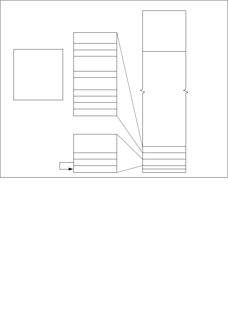
9-32 Vol. 3A
PROCESSOR MANAGEMENT AND INITIALIZATION
Figure 9-6. Task Switching (Lines 282-296 of List File)
GDT RAM RAM_START
TSS RAM
IDT RAM
GDT Alias
IDT Alias
DS
EIP
EFLAGS
CS
SS
0
ES
ESP
•
•
•
•
•
•
SS = TSS.SS
ESP = TSS.ESP
PUSH TSS.EFLAG
PUSH TSS.CS
PUSH TSS.EIP
ES = TSS.ES
DS = TSS.DS
IRET
GDT

Vol. 3A 9-33
PROCESSOR MANAGEMENT AND INITIALIZATION
9.10.3 MAIN.ASM Source Code
The file MAIN.ASM shown in Example 9-2 defines the data and stack segments for this appli-
cation and can be substituted with the main module task written in a high-level language that is
invoked by the IRET instruction executed by STARTUP.ASM.
Example 9-2. MAIN.ASM
NAME main_module
data SEGMENT RW
dw 1000 dup(?)
DATA ENDS
stack stackseg 800
CODE SEGMENT ER use32 PUBLIC
main_start:
nop
nop
nop
CODE ENDS
END main_start, ds:data, ss:stack
9.10.4 Supporting Files
The batch file shown in Example 9-3 can be used to assemble the source code files
STARTUP.ASM and MAIN.ASM and build the final application.
Example 9-3. Batch File to Assemble and Build the Application
ASM386 STARTUP.ASM
ASM386 MAIN.ASM
BLD386 STARTUP.OBJ, MAIN.OBJ buildfile(EPROM.BLD) bootstrap(STARTUP)
Bootload
BLD386 performs several operations in this example:
•It allocates physical memory location to segments and tables.
•It generates tables using the build file and the input files.
•It links object files and resolves references.
•It generates a boot-loadable file to be programmed into the EPROM.
Example 9-4 shows the build file used as an input to BLD386 to perform the above functions.

9-34 Vol. 3A
PROCESSOR MANAGEMENT AND INITIALIZATION
Example 9-4. Build File
INIT_BLD_EXAMPLE;
SEGMENT
*SEGMENTS(DPL = 0)
, startup.startup_code(BASE = 0FFFF0000H)
;
TASK
BOOT_TASK(OBJECT = startup, INITIAL,DPL = 0,
NOT INTENABLED)
, PROTECTED_MODE_TASK(OBJECT = main_module,DPL = 0,
NOT INTENABLED)
;
TABLE
GDT (
LOCATION = GDT_EPROM
, ENTRY = (
10: PROTECTED_MODE_TASK
, startup.startup_code
, startup.startup_data
, main_module.data
, main_module.code
, main_module.stack
)
),
IDT (
LOCATION = IDT_EPROM
);
MEMORY
(
RESERVE = (0..3FFFH
-- Area for the GDT, IDT, TSS copied from
ROM
, 60000H..0FFFEFFFFH)
, RANGE = (ROM_AREA = ROM (0FFFF0000H..0FFFFFFFFH))
-- Eprom size 64K
, RANGE = (RAM_AREA = RAM (4000H..05FFFFH))
);
END
Table 9-5 shows the relationship of each build item with an ASM source file.

Vol. 3A 9-35
PROCESSOR MANAGEMENT AND INITIALIZATION
9.11 MICROCODE UPDATE FACILITIES
The Pentium 4, Intel Xeon, and P6 family processors have the capability to correct errata by
loading an Intel-supplied data block into the processor. The data block is called a microcode
update. This section describes the mechanisms the BIOS needs to provide in order to use this
feature during system initialization. It also describes a specification that permits the incorpora-
tion of future updates into a system BIOS.
Intel considers the release of a microcode update for a silicon revision to be the equivalent of a
processor stepping and completes a full-stepping level validation for releases of microcode
updates.
A microcode update is used to correct errata in the processor. The BIOS, which has an update
loader, is responsible for loading the update on processors during system initialization
(Figure 9-7). There are two steps to this process: the first is to incorporate the necessary update
data blocks into the BIOS; the second is to load update data blocks into the processor.
Table 9-5. Relationship Between BLD Item and ASM Source File
Item ASM386 and Startup.A58 BLD386 Controls
and BLD file Effect
Bootstrap public startup
startup: bootstrap
start(startup) Near jump at
0FFFFFFF0H to start.
GDT location public GDT_EPROM
GDT_EPROM TABLE_REG
<>
TABLE
GDT(location =
GDT_EPROM)
The location of the
GDT will be
programmed into the
GDT_EPROM location.
IDT location public IDT_EPROM
IDT_EPROM TABLE_REG <> TABLE
IDT(location = IDT_EPROM The location of the IDT
will be programmed
into the IDT_EPROM
location.
RAM start RAM_START equ 400H memory (reserve =
(0..3FFFH)) RAM_START is used
as the ram destination
for moving the tables. It
must be excluded from
the application's
segment area.
Location of the
application
TSS in the
GDT
TSS_INDEX EQU 10 TABLE GDT(
ENTRY = (10:
PROTECTED_MODE_
TASK))
Put the descriptor of
the application TSS in
GDT entry 10.
EPROM size
and location size and location of the
initialization code SEGMENT startup.code
(base = 0FFFF0000H)
...memory (RANGE(
ROM_AREA = ROM(x..y))
Initialization code size
must be less than 64K
and resides at upper
most 64K of the 4-
GByte memory space.
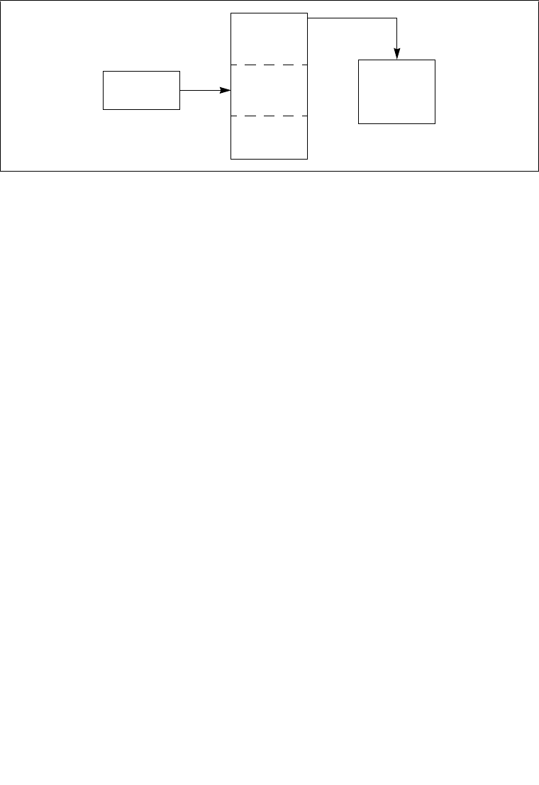
9-36 Vol. 3A
PROCESSOR MANAGEMENT AND INITIALIZATION
9.11.1 Microcode Update
A microcode update consists of an Intel-supplied binary that contains a descriptive header and
data. No executable code resides within the update. Each microcode update is tailored for a
specific list of processor signatures. A mismatch of the processor’s signature with the signature
contained in the update will result in a failure to load. A processor signature includes the
extended family, extended model, type, family, model, and stepping of the processor (starting
with processor family 0fH, model 03H, a given microcode update may be associated with one
of multiple processor signatures; see Section 9.11.2 for detail).
Microcode updates are composed of a multi-byte header, followed by encrypted data and then
by an optional extended signature table. Table 9-6 provides a definition of the fields; Table 9-7
shows the format of an update.
The header is 48 bytes. The first 4 bytes of the header contain the header version. The update
header and its reserved fields are interpreted by software based upon the header version. An
encoding scheme guards against tampering and provides a means for determining the authen-
ticity of any given update. For microcode updates with a data size field equal to 00000000H, the
size of the microcode update is 2048 bytes. The first 48 bytes contain the microcode update
header. The remaining 2000 bytes contain encrypted data.
For microcode updates with a data size not equal to 00000000H, the total size field specifies the
size of the microcode update. The first 48 bytes contain the microcode update header. The
second part of the microcode update is the encrypted data. The data size field of the microcode
update header specifies the encrypted data size, its value must be a multiple of the size of
DWORD. The optional extended signature table if implemented follows the encrypted data, and
its size is calculated by (Total Size – (Data Size + 48)).
NOTE
The optional extended signature table is supported starting with processor
family 0FH, model 03H.
Figure 9-7. Applying Microcode Updates
CPU
BIOS
Update
Blocks
New Update
Update
Loader

Vol. 3A 9-37
PROCESSOR MANAGEMENT AND INITIALIZATION
. Table 9-6. Microcode Update Field Definitions
Field Name Offset
(bytes) Length
(bytes) Description
Header Version 0 4 Version number of the update header.
Update Revision 4 4 Unique version number for the update, the basis for
the update signature provided by the processor to
indicate the current update functioning within the
processor. Used by the BIOS to authenticate the
update and verify that the processor loads
successfully. The value in this field cannot be used for
processor stepping identification alone. This is a
signed 32-bit number.
Date 8 4 Date of the update creation in binary format:
mmddyyyy (e.g. 07/18/98 is 07181998H).
Processor
Signature 12 4 Extended family, extended model, type, family, model,
and stepping of processor that requires this particular
update revision (e.g., 00000650H). Each microcode
update is designed specifically for a given extended
family, extended model, type, family, model, and
stepping of the processor.
The BIOS uses the processor signature field in
conjunction with the CPUID instruction to determine
whether or not an update is appropriate to load on a
processor. The information encoded within this field
exactly corresponds to the bit representations returned
by the CPUID instruction.
Checksum 16 4 Checksum of Update Data and Header. Used to verify
the integrity of the update header and data. Checksum
is correct when the summation of all the DWORDs
(including the extended Processor Signature Table)
that comprise the microcode update result in
00000000H.
Loader Revision 20 4 Version number of the loader program needed to
correctly load this update. The initial version is
00000001H.
Processor Flags 24 4 Platform type information is encoded in the lower 8 bits
of this 4-byte field. Each bit represents a particular
platform type for a given CPUID. The BIOS uses the
processor flags field in conjunction with the platform Id
bits in MSR (17H) to determine whether or not an
update is appropriate to load on a processor. Multiple
bits may be set representing support for multiple
platform IDs.
Data Size 28 4 Specifies the size of the encrypted data in bytes, and
must be a multiple of DWORDs. If this value is
00000000H, then the microcode update encrypted
data is 2000 bytes (or 500 DWORDs).

9-38 Vol. 3A
PROCESSOR MANAGEMENT AND INITIALIZATION
Total Size 32 4 Specifies the total size of the microcode update in
bytes. It is the summation of the header size, the
encrypted data size and the size of the optional
extended signature table.
Reserved 36 12 Reserved fields for future expansion
Update Data 48 Data Size
or 2000 Update data
Extended
Signature Count Data Size +
48 4 Specifies the number of extended signature structures
(Processor Signature[n], processor flags[n] and
checksum[n]) that exist in this microcode update.
Extended
Checksum Data Size +
52 4 Checksum of update extended processor signature
table. Used to verify the integrity of the extended
processor signature table. Checksum is correct when
the summation of the DWORDs that comprise the
extended processor signature table results in
00000000H.
Reserved Data Size +
56 12 Reserved fields
Processor
Signature[n] Data Size +
68 + (n * 12) 4Extended family, extended model, type, family, model,
and stepping of processor that requires this particular
update revision (e.g., 00000650H). Each microcode
update is designed specifically for a given extended
family, extended model, type, family, model, and
stepping of the processor.
The BIOS uses the processor signature field in
conjunction with the CPUID instruction to determine
whether or not an update is appropriate to load on a
processor. The information encoded within this field
exactly corresponds to the bit representations returned
by the CPUID instruction.
Processor Flags[n] Data Size +
72 + (n * 12) 4 Platform type information is encoded in the lower 8 bits
of this 4-byte field. Each bit represents a particular
platform type for a given CPUID. The BIOS uses the
processor flags field in conjunction with the platform Id
bits in MSR (17H) to determine whether or not an
update is appropriate to load on a processor. Multiple
bits may be set representing support for multiple
platform IDs.
Table 9-6. Microcode Update Field Definitions (Contd.)
Field Name Offset
(bytes) Length
(bytes) Description
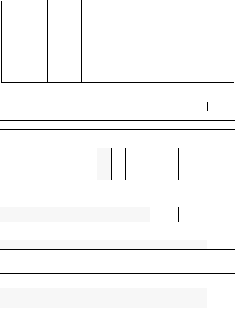
Vol. 3A 9-39
PROCESSOR MANAGEMENT AND INITIALIZATION
Checksum[n] Data Size +
76 + (n * 12) 4 Used by utility software to decompose a microcode
update into multiple microcode updates where each of
the new updates is constructed without the optional
Extended Processor Signature Table.
To calculate the Checksum, substitute the Primary
Processor Signature entry and the Processor Flags
entry with the corresponding Extended Patch entry.
Delete the Extended Processor Signature Table
entries. The Checksum is correct when the summation
of all DWORDs that comprise the created Extended
Processor Patch results in 00000000H.
Table 9-7. Microcode Update Format
31 24 16 8 0 Bytes
Header Version 0
Update Revision 4
Month: 8 Day: 8 Year: 16 8
Processor Signature (CPUID) 12
Res: 4
Extended
Family: 8
Extended
Mode: 4
Reserved: 2
Type: 2
Family: 4
Model: 4
Stepping: 4
Checksum 16
Loader Revision 20
Processor Flags 24
Reserved (24 bits)
P7
P6
P5
P4
P3
P2
P1
P0
Data Size 28
Total Size 32
Reserved (12 Bytes) 36
Update Data (Data Size bytes, or 2000 Bytes if Data Size = 00000000H) 48
Extended Signature Count ‘n’ Data Size
+ 48
Extended Processor Signature Table Checksum Data Size
+ 52
Reserved (12 Bytes) Data Size
+ 56
Table 9-6. Microcode Update Field Definitions (Contd.)
Field Name Offset
(bytes) Length
(bytes) Description

9-40 Vol. 3A
PROCESSOR MANAGEMENT AND INITIALIZATION
9.11.2 Optional Extended Signature Table
The extended signature table is a structure that may be appended to the end of the encrypted data
when the encrypted data only supports a single processor signature (optional case). The
extended signature table will always be present when the encrypted data supports multiple
processor steppings and/or models (required case).
The extended signature table consists of a 20-byte extended signature header structure, which
contains the extended signature count, the extended processor signature table checksum, and 12
reserved bytes (Table 9-8). Following the extended signature header structure, the extended
signature table contains 0-to-n extended processor signature structures.
Each processor signature structure consist of the processor signature, processor flags, and a
checksum (Table 9-9).
The extended signature count in the extended signature header structure indicates the number of
processor signature structures that exist in the extended signature table.
The extended processor signature table checksum is a checksum of all DWORDs that comprise
the extended signature table. That includes the extended signature count, extended processor
signature table checksum, 12 reserved bytes and the n processor signature structures. A valid
extended signature table exists when the result of a DWORD checksum is 00000000H.
Processor Signature[n] Data Size
+ 68 +
(n * 12)
Processor Flags[n] Data Size
+ 72 +
(n * 12)
Checksum[n] Data Size
+ 76 +
(n * 12)
Table 9-8. Extended Processor Signature Table Header Structure
Extended Signature Count ‘n’ Data Size + 48
Extended Processor Signature Table Checksum Data Size + 52
Reserved (12 Bytes) Data Size + 56
Table 9-9. Processor Signature Structure
Processor Signature[n] Data Size + 68 + (n * 12)
Processor Flags[n] Data Size + 72 + (n * 12)
Checksum[n] Data Size + 76 + (n * 12)
Table 9-7. Microcode Update Format (Contd.)
31 24 16 8 0 Bytes

Vol. 3A 9-41
PROCESSOR MANAGEMENT AND INITIALIZATION
9.11.3 Processor Identification
Each microcode update is designed to for a specific processor or set of processors. To determine
the correct microcode update to load, software must ensure that one of the processor signatures
embedded in the microcode update matches the 32-bit processor signature returned by the
CPUID instruction when executed by the target processor with EAX = 1. Attempting to load a
microcode update that does not match a processor signature embedded in the microcode update
with the processor signature returned by CPUID will cause the processor to reject the update.
Example 9-5 shows how to check for a valid processor signature match between the processor
and microcode update.
Example 9-5. Pseudo Code to Validate the Processor Signature
ProcessorSignature ← CPUID(1):EAX
If (Update.HeaderVersion == 00000001h)
{
// first check the ProcessorSignature field
If (ProcessorSignature == Update.ProcessorSignature)
Success
// if extended signature is present
Else If (Update.TotalSize > (Update.DataSize + 48))
{
//
// Assume the Data Size has been used to calculate the
// location of Update.ProcessorSignature[0].
//
For (N ← 0; ((N < Update.ExtendedSignatureCount) AND
(ProcessorSignature != Update.ProcessorSignature[N])); N++);
// if the loops ended when the iteration count is
// less than the number of processor signatures in
// the table, we have a match
If (N < Update.ExtendedSignatureCount)
Success
Else
Fail
}
Else
Fail
Else
Fail

9-42 Vol. 3A
PROCESSOR MANAGEMENT AND INITIALIZATION
9.11.4 Platform Identification
In addition to verifying the processor signature, the intended processor platform type must be
determined to properly target the microcode update. The intended processor platform type is
determined by reading the IA32_PLATFORM_ID register, (MSR 17H). This 64-bit register
must be read using the RDMSR instruction.
The three platform ID bits, when read as a binary coded decimal (BCD) number, indicate the bit
position in the microcode update header’s processor flags field associated with the installed
processor. The processor flags in the 48-byte header and the processor flags field associated
with the extended processor signature structures may have multiple bits set. Each set bit repre-
sents a different platform ID that the update supports.
Register Name: IA32_PLATFORM_ID
MSR Address: 017H
Access: Read Only
IA32_PLATFORM_ID is a 64-bit register accessed only when referenced as a Qword through a
RDMSR instruction.
To validate the platform information, software may implement an algorithm similar to the algo-
rithms in Example 9-6.
Table 9-10. Processor Flags
Bit Descriptions
63:53 Reserved
52:50 Platform Id Bits (RO). The field gives information concerning the intended platform for the
processor. See also Table 9-7.
5251 50
000Processor Flag 0
001Processor Flag 1
010Processor Flag 2
011Processor Flag 3
100Processor Flag 4
101Processor Flag 5
110Processor Flag 6
111Processor Flag 7
49:0 Reserved

Vol. 3A 9-43
PROCESSOR MANAGEMENT AND INITIALIZATION
Example 9-6. Pseudo Code Example of Processor Flags Test
Flag ← 1 << IA32_PLATFORM_ID[52:50]
If (Update.HeaderVersion == 00000001h)
{
If (Update.ProcessorFlags & Flag)
{
Load Update
}
Else
{
//
// Assume the Data Size has been used to calculate the
// location of Update.ProcessorSignature[N] and a match
// on Update.ProcessorSignature[N] has already succeeded
//
If (Update.ProcessorFlags[n] & Flag)
{
Load Update
}
}
}
9.11.5 Microcode Update Checksum
Each microcode update contains a DWORD checksum located in the update header. It is soft-
ware’s responsibility to ensure that a microcode update is not corrupt. To check for a corrupt
microcode update, software must perform a unsigned DWORD (32-bit) checksum of the micro-
code update. Even though some fields are signed, the checksum procedure treats all DWORDs
as unsigned. Microcode updates with a header version equal to 00000001H must sum all
DWORDs that comprise the microcode update. A valid checksum check will yield a value of
00000000H. Any other value indicates the microcode update is corrupt and should not be
loaded.
The checksum algorithm shown by the pseudo code in Example 9-7 treats the microcode update
as an array of unsigned DWORDs. If the data size DWORD field at byte offset 32 equals
00000000H, the size of the encrypted data is 2000 bytes, resulting in 500 DWORDs. Otherwise
the microcode update size in DWORDs = (Total Size / 4).

9-44 Vol. 3A
PROCESSOR MANAGEMENT AND INITIALIZATION
Example 9-7. Pseudo Code Example of Checksum Test
N ← 512
If (Update.DataSize != 00000000H)
N ← Update.TotalSize / 4
ChkSum ← 0
For (I ← 0; I < N; I++)
{
ChkSum ← ChkSum + MicrocodeUpdate[I]
}
If (ChkSum == 00000000H)
Success
Else
Fail
9.11.6 Microcode Update Loader
This section describes an update loader used to load an update into a Pentium 4, Intel Xeon, or
P6 family processor. It also discusses the requirements placed on the BIOS to ensure proper
loading. The update loader described contains the minimal instructions needed to load an
update. The specific instruction sequence that is required to load an update is dependent upon
the loader revision field contained within the update header. This revision is expected to change
infrequently (potentially, only when new processor models are introduced).
Example 9-8 below represents the update loader with a loader revision of 00000001H. Note that
the microcode update must be aligned on a 16-byte boundary.
Example 9-8. Assembly Code Example of Simple Microcode Update Loader
mov ecx,79h ; MSR to read in ECX
xor eax,eax ; clear EAX
xor ebx,ebx ; clear EBX
mov ax,cs ; Segment of microcode update
shl eax,4
mov bx,offset Update ; Offset of microcode update
add eax,ebx ; Linear Address of Update in EAX
add eax,48d ; Offset of the Update Data within the Update
xor edx,edx ; Zero in EDX
WRMSR ; microcode update trigger

Vol. 3A 9-45
PROCESSOR MANAGEMENT AND INITIALIZATION
The loader shown in Example 9-8 assumes that update is the address of a microcode update
(header and data) embedded within the code segment of the BIOS. It also assumes that the
processor is operating in real mode. The data may reside anywhere in memory, aligned on a
16-byte boundary, that is accessible by the processor within its current operating mode (real,
protected).
Before the BIOS executes the microcode update trigger (WRMSR) instruction, the following
must be true:
•EAX contains the linear address of the start of the update data
•EDX contains zero
•ECX contains 79H (address of IA32_BIOS_UPDT_TRIG)
Other requirements are:
•If the update is loaded while the processor is in real mode, then the update data may not
cross a segment boundary.
•If the update is loaded while the processor is in real mode, then the update data may not
exceed a segment limit.
•If paging is enabled, pages that are currently present must map the update data.
•The microcode update data requires a 16-byte boundary alignment.
9.11.6.1 Hard Resets in Update Loading
The effects of a loaded update are cleared from the processor upon a hard reset. Therefore, each
time a hard reset is asserted during the BIOS POST, the update must be reloaded on all proces-
sors that observed the reset. The effects of a loaded update are, however, maintained across a
processor INIT. There are no side effects caused by loading an update into a processor multiple
times.
9.11.6.2 Update in a Multiprocessor System
A multiprocessor (MP) system requires loading each processor with update data appropriate for
its CPUID and platform ID bits. The BIOS is responsible for ensuring that this requirement is
met and that the loader is located in a module executed by all processors in the system. If a
system design permits multiple steppings of Pentium 4, Intel Xeon, and P6 family processors to
exist concurrently; then the BIOS must verify individual processors against the update header
information to ensure appropriate loading. Given these considerations, it is most practical to
load the update during MP initialization.

9-46 Vol. 3A
PROCESSOR MANAGEMENT AND INITIALIZATION
9.11.6.3 Update in a System Supporting Intel Hyper-Threading Technology
Intel Hyper-Threading Technology has implications on the loading of the microcode update.
The update must be loaded for each core in a physical processor. Thus, for a processor
supporting Hyper-Threading Technology, only one logical processor per core is required to load
the microcode update. Each individual logical processor can independently load the update.
However, MP initialization must provide some mechanism (e.g. a software semaphore) to force
serialization of microcode update loads and to prevent simultaneous load attempts to the same
core.
9.11.6.4 Update in a System Supporting Dual-Core Technology
Dual-core technology has implications on the loading of the microcode update. The microcode
update facility is not shared between processor cores in the same physical package. The update
must be loaded for each core in a physical processor.
If processor core supports Hyper-Threading Technology, the guideline described in Section
9.11.6.3 also applies.
9.11.6.5 Update Loader Enhancements
The update loader presented in Section 9.11.6, “Microcode Update Loader,” is a minimal imple-
mentation that can be enhanced to provide additional functionality. Potential enhancements are
described below:
•BIOS can incorporate multiple updates to support multiple steppings of the Pentium 4,
Intel Xeon, and P6 family processors. This feature provides for operating in a mixed
stepping environment on an MP system and enables a user to upgrade to a later version of
the processor. In this case, modify the loader to check the CPUID and platform ID bits of
the processor that it is running on against the available headers before loading a particular
update. The number of updates is only limited by available BIOS space.
•A loader can load the update and test the processor to determine if the update was loaded
correctly. See Section 9.11.7, “Update Signature and Verification.”
•A loader can verify the integrity of the update data by performing a checksum on the
double words of the update summing to zero. See Section 9.11.5, “Microcode Update
Checksum.”
•A loader can provide power-on messages indicating successful loading of an update.
9.11.7 Update Signature and Verification
The Pentium 4, Intel Xeon, and P6 family processors provide capabilities to verify the authen-
ticity of a particular update and to identify the current update revision. This section describes the
model-specific extensions of processors that support this feature. The update verification
method below assumes that the BIOS will only verify an update that is more recent than the revi-
sion currently loaded in the processor.

Vol. 3A 9-47
PROCESSOR MANAGEMENT AND INITIALIZATION
CPUID returns a value in a model specific register in addition to its usual register return values.
The semantics of CPUID cause it to deposit an update ID value in the 64-bit model-specific
register at address 08BH (IA32_BIOS_SIGN_ID). If no update is present in the processor, the
value in the MSR remains unmodified. The BIOS must pre-load a zero into the MSR before
executing CPUID. If a read of the MSR at 8BH still returns zero after executing CPUID, this
indicates that no update is present.
The update ID value returned in the EDX register after RDMSR executes indicates the revision
of the update loaded in the processor. This value, in combination with the CPUID value returned
in the EAX register, uniquely identifies a particular update. The signature ID can be directly
compared with the update revision field in a microcode update header for verification of a
correct load. No consecutive updates released for a given stepping of a processor may share the
same signature. The processor signature returned by CPUID differentiates updates for different
steppings.
9.11.7.1 Determining the Signature
An update that is successfully loaded into the processor provides a signature that matches the
update revision of the currently functioning revision. This signature is available any time after
the actual update has been loaded. Requesting the signature does not have a negative impact
upon a loaded update.
The procedure for determining this signature shown in Example 9-9.
Example 9-9. Assembly Code to Retrieve the Update Revision
MOV ECX, 08BH ;IA32_BIOS_SIGN_ID
XOR EAX, EAX ;clear EAX
XOR EDX, EDX ;clear EDX
WRMSR ;Load 0 to MSR at 8BH
MOV EAX, 1
cpuid
MOV ECX, 08BH ;IA32_BIOS_SIGN_ID
rdmsr ;Read Model Specific Register
If there is an update active in the processor, its revision is returned in the EDX register after the
RDMSR instruction executes.
IA32_BIOS_SIGN_ID Microcode Update Signature Register
MSR Address: 08BH Accessed as a Qword
Default Value: XXXX XXXX XXXX XXXXh
Access: Read/Write

9-48 Vol. 3A
PROCESSOR MANAGEMENT AND INITIALIZATION
The IA32_BIOS_SIGN_ID register is used to report the microcode update signature when
CPUID executes. The signature is returned in the upper DWORD (Table 9-11).
9.11.7.2 Authenticating the Update
An update may be authenticated by the BIOS using the signature primitive, described above, and
the algorithm in Example 9-10.
Example 9-10. Pseudo Code to Authenticate the Update
Z ← Obtain Update Revision from the Update Header to be authenticated;
X ← Obtain Current Update Signature from MSR 8BH;
If (Z > X)
{
Load Update that is to be authenticated;
Y ← Obtain New Signature from MSR 8BH;
If (Z == Y)
Success
Else
Fail
}
Else
Fail
Example 9-10 requires that the BIOS only authenticate updates that contain a numerically larger
revision than the currently loaded revision, where Current Signature (X) < New Update Revi-
sion (Z). A processor with no loaded update is considered to have a revision equal to zero.
This authentication procedure relies upon the decoding provided by the processor to verify an
update from a potentially hostile source. As an example, this mechanism in conjunction with
other safeguards provides security for dynamically incorporating field updates into the BIOS.
Table 9-11. Microcode Update Signature
Bit Description
63:32 Microcode update signature. This field contains the signature of the currently loaded
microcode update when read following the execution of the CPUID instruction, function 1. It is
required that this register field be pre-loaded with zero prior to executing the CPUID,
function 1. If the field remains equal to zero, then there is no microcode update loaded.
Another non-zero value will be the signature.
31:0 Reserved.

Vol. 3A 9-49
PROCESSOR MANAGEMENT AND INITIALIZATION
9.11.8 Pentium 4, Intel Xeon, and P6 Family Processor
Microcode Update Specifications
This section describes the interface that an application can use to dynamically integrate
processor-specific updates into the system BIOS. In this discussion, the application is referred
to as the calling program or caller.
The real mode INT15 call specification described here is an Intel extension to an OEM BIOS.
This extension allows an application to read and modify the contents of the microcode update
data in NVRAM. The update loader, which is part of the system BIOS, cannot be updated by the
interface. All of the functions defined in the specification must be implemented for a system to
be considered compliant with the specification. The INT15 functions are accessible only from
real mode.
9.11.8.1 Responsibilities of the BIOS
If a BIOS passes the presence test (INT 15H, AX = 0D042H, BL = 0H), it must implement all
of the sub-functions defined in the INT 15H, AX = 0D042H specification. There are no optional
functions. BIOS must load the appropriate update for each processor during system initialization.
A Header Version of an update block containing the value 0FFFFFFFFH indicates that the
update block is unused and available for storing a new update.
The BIOS is responsible for providing a region of non-volatile storage (NVRAM) for each
potential processor stepping within a system. This storage unit consists of one or more update
blocks. An update block is a contiguous 2048-byte block of memory. The BIOS for a single
processor system need only provide update blocks to store one microcode update. If the BIOS
for a multiple processor system is intended to support mixed processor steppings, then the BIOS
needs to provide enough update blocks to store each unique microcode update or for each
processor socket on the OEM’s system board.
The BIOS is responsible for managing the NVRAM update blocks. This includes garbage
collection, such as removing microcode updates that exist in NVRAM for which a corre-
sponding processor does not exist in the system. This specification only provides the mechanism
for ensuring security, the uniqueness of an entry, and that stale entries are not loaded. The actual
update block management is implementation specific on a per-BIOS basis.
As an example, the BIOS may use update blocks sequentially in ascending order with CPU
signatures sorted versus the first available block. In addition, garbage collection may be imple-
mented as a setup option to clear all NVRAM slots or as BIOS code that searches and eliminates
unused entries during boot.
NOTES
For IA-32 processors starting with family 0FH and model 03H, the
microcode update may be as large as 16 KBytes. Thus, BIOS must allocate 8

9-50 Vol. 3A
PROCESSOR MANAGEMENT AND INITIALIZATION
update blocks for each microcode update. In a MP system, a common
microcode update may be sufficient for each socket in the system.
For IA-32 processors earlier than family 0FH and model 03H, the microcode
update is 2 KBytes. An MP-capable BIOS that supports multiple steppings
must allocate a block for each socket in the system.
A single-processor BIOS that supports variable-sized microcode update and
fixed-sized microcode update must allocate one 16-KByte region and a
second region of at least 2 KBytes.
The following algorithm (Example 9-11) describes the steps performed during BIOS initializa-
tion used to load the updates into the processor(s). The algorithm assumes:
•The BIOS ensures that no update contained within NVRAM has a header version or loader
version that does not match one currently supported by the BIOS.
•The update contains a correct checksum.
•The BIOS ensures that (at most) one update exists for each processor stepping.
•Older update revisions are not allowed to overwrite more recent ones.
These requirements are checked by the BIOS during the execution of the write update function
of this interface. The BIOS sequentially scans through all of the update blocks in NVRAM
starting with index 0. The BIOS scans until it finds an update where the processor fields in the
header match the processor signature (extended family, extended model, type, family, model,
and stepping) as well as the platform bits of the current processor.
Example 9-11. Pseudo Code, Checks Required Prior to Loading an Update
For each processor in the system
{
Determine the Processor Signature via CPUID function 1;
Determine the Platform Bits ← 1 << IA32_PLATFORM_ID[52:50];
For (I ← UpdateBlock 0, I < NumOfBlocks; I++)
{
If (Update.Header_Version == 0x00000001)
{
If ((Update.ProcessorSignature == Processor Signature) &&
(Update.ProcessorFlags & Platform Bits))
{
Load Update.UpdateData into the Processor;
Verify update was correctly loaded into the processor
Go on to next processor
Break;
}
Else If (Update.TotalSize > (Update.DataSize + 48))
{
N ← 0
While (N < Update.ExtendedSignatureCount)

Vol. 3A 9-51
PROCESSOR MANAGEMENT AND INITIALIZATION
{
If ((Update.ProcessorSignature[N] ==
Processor Signature) &&
(Update.ProcessorFlags[N] & Platform Bits))
{
Load Update.UpdateData into the Processor;
Verify update was correctly loaded into the processor
Go on to next processor
Break;
}
N ← N + 1
}
I ← I + (Update.TotalSize / 2048)
If ((Update.TotalSize MOD 2048) == 0)
I ← I + 1
}
}
}
}
NOTES
The platform Id bits in IA32_PLATFORM_ID are encoded as a three-bit
binary coded decimal field. The platform bits in the microcode update header
are individually bit encoded. The algorithm must do a translation from one
format to the other prior to doing a check.
When performing the INT 15H, 0D042H functions, the BIOS must assume that the caller has
no knowledge of platform specific requirements. It is the responsibility of BIOS calls to manage
all chipset and platform specific prerequisites for managing the NVRAM device. When writing
the update data using the Write Update sub-function, the BIOS must maintain implementation
specific data requirements (such as the update of NVRAM checksum). The BIOS should also
attempt to verify the success of write operations on the storage device used to record the update.
9.11.8.2 Responsibilities of the Calling Program
This section of the document lists the responsibilities of a calling program using the interface
specifications to load microcode update(s) into BIOS NVRAM.
•The calling program should call the INT 15H, 0D042H functions from a pure real mode
program and should be executing on a system that is running in pure real mode.
•The caller should issue the presence test function (sub function 0) and verify the signature
and return codes of that function.
•It is important that the calling program provides the required scratch RAM buffers for the
BIOS and the proper stack size as specified in the interface definition.

9-52 Vol. 3A
PROCESSOR MANAGEMENT AND INITIALIZATION
•The calling program should read any update data that already exists in the BIOS in order to
make decisions about the appropriateness of loading the update. The BIOS must refuse to
overwrite a newer update with an older version. The update header contains information
about version and processor specifics for the calling program to make an intelligent
decision about loading.
•There can be no ambiguous updates. The BIOS must refuse to allow multiple updates for
the same CPU to exist at the same time; it also must refuse to load updates for processors
that don’t exist on the system.
•The calling application should implement a verify function that is run after the update
write function successfully completes. This function reads back the update and verifies that
the BIOS returned an image identical to the one that was written.
Example 9-12 represents a calling program.
Example 9-12. INT 15 DO42 Calling Program Pseudo-code
//
// We must be in real mode
//
If the system is not in Real mode exit
//
// Detect the presence of Genuine Intel processor(s) that can be updated
// using(CPUID)
//
If no Intel processors exist that can be updated exit
//
// Detect the presence of the Intel microcode update extensions
//
If the BIOS fails the PresenceTestexit
//
// If the APIC is enabled, see if any other processors are out there
//
Read IA32_APICBASE
If APIC enabled
{
Send Broadcast Message to all processors except self via APIC
Have all processors execute CPUID and record the Processor Signature
(i.e.,Extended Family, Extended Model, Type, Family, Model, Stepping)
Have all processors read IA32_PLATFORM_ID[52:50] and record Platform
Id Bits
If current processor cannot be updated
exit
}
//
// Determine the number of unique update blocks needed for this system
//
NumBlocks = 0

Vol. 3A 9-53
PROCESSOR MANAGEMENT AND INITIALIZATION
For each processor
{
If ((this is a unique processor stepping) AND
(we have a unique update in the database for this processor))
{
Checksum the update from the database;
If Checksum fails
exit
NumBlocks ← NumBlocks + size of microcode update / 2048
}
}
//
// Do we have enough update slots for all CPUs?
//
If there are more blocks required to support the unique processor steppings
than update blocks provided by the BIOS
exit
//
// Do we need any update blocks at all? If not, we are done
//
If (NumBlocks == 0)
exit
//
// Record updates for processors in NVRAM.
//
For (I=0; I<NumBlocks; I++)
{
//
// Load each Update
//
Issue the WriteUpdate function
If (STORAGE_FULL) returned
{
Display Error -- BIOS is not managing NVRAM appropriately
exit
}
If (INVALID_REVISION) returned
{
Display Message: More recent update already loaded in NVRAM for
this stepping
continue
}
If any other error returned
{
Display Diagnostic
exit

9-54 Vol. 3A
PROCESSOR MANAGEMENT AND INITIALIZATION
}
//
// Verify the update was loaded correctly
//
Issue the ReadUpdate function
If an error occurred
{
Display Diagnostic
exit
}
//
// Compare the Update read to that written
//
If (Update read != Update written)
{
Display Diagnostic
exit
}
I ← I + (size of microcode update / 2048)
}
//
// Enable Update Loading, and inform user
//
Issue the Update Control function with Task = Enable.
9.11.8.3 Microcode Update Functions
Table 9-12 defines current Pentium 4, Intel Xeon, and P6 family processor microcode update
functions.
Table 9-12. Microcode Update Functions
Microcode Update
Function Function
Number Description Required/Optional
Presence test 00H Returns information about the supported
functions. Required
Write update data 01H Writes one of the update data areas (slots). Required
Update control 02H Globally controls the loading of updates. Required
Read update data 03H Reads one of the update data areas (slots). Required

Vol. 3A 9-55
PROCESSOR MANAGEMENT AND INITIALIZATION
9.11.8.4 INT 15H-based Interface
Intel recommends that a BIOS interface be provided that allows additional microcode updates
to be added to system flash. The INT15H interface is the Intel-defined method for doing this.
The program that calls this interface is responsible for providing three 64-kilobyte RAM areas
for BIOS use during calls to the read and write functions. These RAM scratch pads can be used
by the BIOS for any purpose, but only for the duration of the function call. The calling routine
places real mode segments pointing to the RAM blocks in the CX, DX and SI registers. Calls to
functions in this interface must be made with a minimum of 32 kilobytes of stack available to
the BIOS.
In general, each function returns with CF cleared and AH contains the returned status. The
general return codes and other constant definitions are listed in Section 9.11.8.9, “Return Codes.”
The OEM error field (AL) is provided for the OEM to return additional error information
specific to the platform. If the BIOS provides no additional information about the error, OEM
error must be set to SUCCESS. The OEM error field is undefined if AH contains either
SUCCESS (00H) or NOT_IMPLEMENTED (86H). In all other cases, it must be set with either
SUCCESS or a value meaningful to the OEM.
The following sections describe functions provided by the INT15H-based interface.
9.11.8.5 Function 00H—Presence Test
This function verifies that the BIOS has implemented required microcode update functions.
Table 9-13 lists the parameters and return codes for the function.
Table 9-13. Parameters for the Presence Test
Input
AX Function Code 0D042H
BL Sub-function 00H - Presence test
Output
CF Carry Flag Carry Set - Failure - AH contains status
Carry Clear - All return values valid
AH Return Code
AL OEM Error Additional OEM information.
EBX Signature Part 1 'INTE' - Part one of the signature
ECX Signature Part 2 'LPEP'- Part two of the signature
EDX Loader Version Version number of the microcode update loader
SI Update Count Number of 2048 update blocks in NVRAM the BIOS allocated
to storing microcode updates
Return Codes (see Table 9-18 for code definitions
SUCCESS The function completed successfully.
NOT_IMPLEMENTED The function is not implemented.

9-56 Vol. 3A
PROCESSOR MANAGEMENT AND INITIALIZATION
Description
In order to assure that the BIOS function is present, the caller must verify the carry flag, the
return code, and the 64-bit signature. The update count reflects the number of 2048-byte blocks
available for storage within one non-volatile RAM.
The loader version number refers to the revision of the update loader program that is included
in the system BIOS image.
9.11.8.6 Function 01H—Write Microcode Update Data
This function integrates a new microcode update into the BIOS storage device. Table 9-14 lists
the parameters and return codes for the function.
Table 9-14. Parameters for the Write Update Data Function
Input
AX Function Code 0D042H
BL Sub-function 01H - Write update
ES:DI Update Address Real Mode pointer to the Intel Update structure. This buffer is
2048 bytes in length if the processor supports only fixed-size
microcode update or...
Real Mode pointer to the Intel Update structure. This buffer is
64 KBytes in length if the processor supports a variable-size
microcode update.
CX Scratch Pad1 Real mode segment address of 64 KBytes of RAM block
DX Scratch Pad2 Real mode segment address of 64 KBytes of RAM block
SI Scratch Pad3 Real mode segment address of 64 KBytes of RAM block
SS:SP Stack pointer 32 KBytes of stack minimum
Output
CF Carry Flag Carry Set - Failure - AH Contains status
Carry Clear - All return values valid
AH Return Code Status of the call
AL OEM Error Additional OEM information
Return Codes (see Table 9-18 for code definitions
SUCCESS The function completed successfully.
NOT_IMPLEMENTED The function is not implemented.
WRITE_FAILURE A failure occurred because of the inability to write the storage
device.
ERASE_FAILURE A failure occurred because of the inability to erase the storage
device.
READ_FAILURE A failure occurred because of the inability to read the storage
device.

Vol. 3A 9-57
PROCESSOR MANAGEMENT AND INITIALIZATION
Description
The BIOS is responsible for selecting an appropriate update block in the non-volatile storage for
storing the new update. This BIOS is also responsible for ensuring the integrity of the informa-
tion provided by the caller, including authenticating the proposed update before incorporating it
into storage.
Before writing the update block into NVRAM, the BIOS should ensure that the update structure
meets the following criteria in the following order:
1. The update header version should be equal to an update header version recognized by the
BIOS.
2. The update loader version in the update header should be equal to the update loader
version contained within the BIOS image.
3. The update block must checksum. This checksum is computed as a 32-bit summation of all
double words in the structure, including the header, data, and processor signature table.
The BIOS selects update block(s) in non-volatile storage for storing the candidate update. The
BIOS can select any available update block as long as it guarantees that only a single update
exists for any given processor stepping in non-volatile storage. If the update block selected
already contains an update, the following additional criteria apply to overwrite it:
•The processor signature in the proposed update must be equal to the processor signature in
the header of the current update in NVRAM (Processor Signature + platform ID bits).
•The update revision in the proposed update should be greater than the update revision in
the header of the current update in NVRAM.
STORAGE_FULL The BIOS non-volatile storage area is unable to accommodate
the update because all available update blocks are filled with
updates that are needed for processors in the system.
CPU_NOT_PRESENT The processor stepping does not currently exist in the system.
INVALID_HEADER The update header contains a header or loader version that is
not recognized by the BIOS.
INVALID_HEADER_CS The update does not checksum correctly.
SECURITY_FAILURE The processor rejected the update.
INVALID_REVISION The same or more recent revision of the update exists in the
storage device.
Table 9-14. Parameters for the Write Update Data Function (Contd.)
Input

9-58 Vol. 3A
PROCESSOR MANAGEMENT AND INITIALIZATION
If no unused update blocks are available and the above criteria are not met, the BIOS can over-
write update block(s) for a processor stepping that is no longer present in the system. This can
be done by scanning the update blocks and comparing the processor steppings, identified in the
MP Specification table, to the processor steppings that currently exist in the system.
Finally, before storing the proposed update in NVRAM, the BIOS must verify the authenticity
of the update via the mechanism described in Section 9.11.6, “Microcode Update Loader.” This
includes loading the update into the current processor, executing the CPUID instruction, reading
MSR 08Bh, and comparing a calculated value with the update revision in the proposed update
header for equality.
When performing the write update function, the BIOS must record the entire update, including
the header, the update data, and the extended processor signature table (if applicable). When
writing an update, the original contents may be overwritten, assuming the above criteria have
been met. It is the responsibility of the BIOS to ensure that more recent updates are not over-
written through the use of this BIOS call, and that only a single update exists within the NVRAM
for any processor stepping and platform ID.
Figure 9-8 and Figure 9-9 show the process the BIOS follows to choose an update block and
ensure the integrity of the data when it stores the new microcode update.
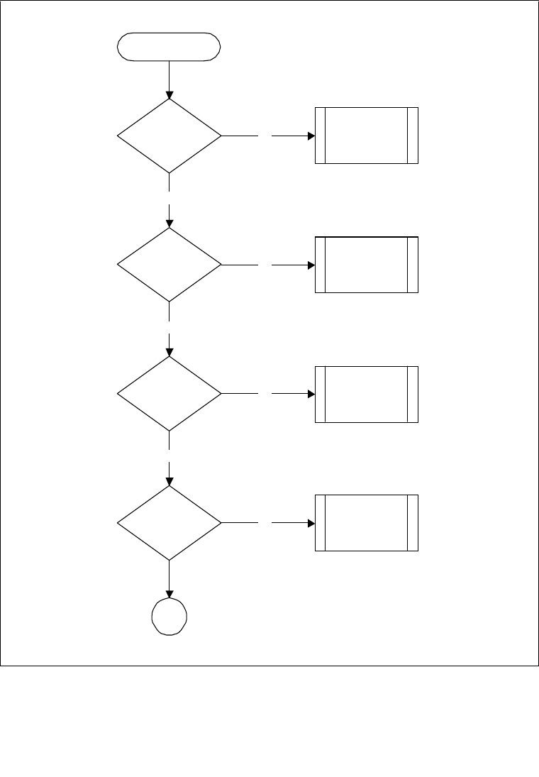
Vol. 3A 9-59
PROCESSOR MANAGEMENT AND INITIALIZATION
Figure 9-8. Microcode Update Write Operation Flow [1]
1
V
a
lid
U
p
d
ate
Header Version?
Loader Revision Match
BIOS’s Loader?
Does Update Match A
CPU in The System
Write Microcode Update
Does Update
Checksum Correctly?
Yes
Yes
Yes
N
o
R
eturn
CPU_NOT_PRESENT
No
Return
INVALID_HEADER
N
o
Return
INVALID_HEADER
N
o
R
eturn
INVALID_HEADER_ CS
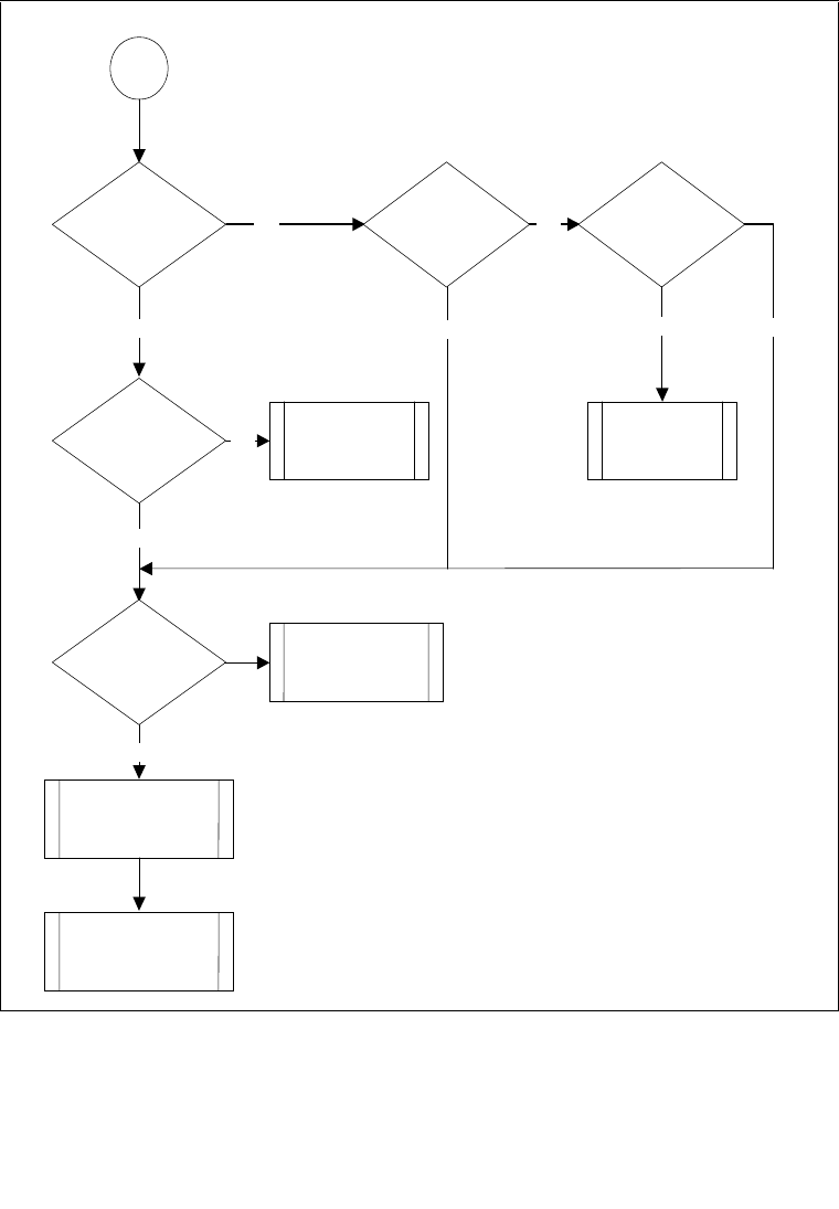
9-60 Vol. 3A
PROCESSOR MANAGEMENT AND INITIALIZATION
Figure 9-9. Microcode Update Write Operation Flow [2]
Return
INVALID_REVISION
Yes
1
Update Revision Newer
Than NVRAM Update?
Update Pass
A
uthenticity Test? Return
SECURITY_FAILURE
Yes
Update NMRAM Record
Return
SUCCESS
Update Matching CPU
A
lready In NVRAM? Space Available in
NVRAM?
Yes
No
Return
STORAGE_FULL
Replacement
policy implemented?
No
No
No
Yes Yes

Vol. 3A 9-61
PROCESSOR MANAGEMENT AND INITIALIZATION
9.11.8.7 Function 02H—Microcode Update Control
This function enables loading of binary updates into the processor. Table 9-15 lists the parame-
ters and return codes for the function.
Description
This control is provided on a global basis for all updates and processors. The caller can deter-
mine the current status of update loading (enabled or disabled) without changing the state. The
function does not allow the caller to disable loading of binary updates, as this poses a security
risk.
The caller specifies the requested operation by placing one of the values from Table 9-16 in the
BH register. After successfully completing this function, the BL register contains either the
enable or the disable designator. Note that if the function fails, the update status return value is
undefined.
Table 9-15. Parameters for the Control Update Sub-function
Input
AX Function Code 0D042H
BL Sub-function 02H - Control update
BH Task See the description below.
CX Scratch Pad1 Real mode segment of 64 KBytes of RAM block
DX Scratch Pad2 Real mode segment of 64 KBytes of RAM block
SI Scratch Pad3 Real mode segment of 64 KBytes of RAM block
SS:SP Stack pointer 32 kilobytes of stack minimum
Output
CF Carry Flag Carry Set - Failure - AH contains status
Carry Clear - All return values valid.
AH Return Code Status of the call
AL OEM Error Additional OEM Information.
BL Update Status Either enable or disable indicator
Return Codes (see Table 9-18 for code definitions)
SUCCESS Function completed successfully.
READ_FAILURE A failure occurred because of the inability to read the storage
device.
Table 9-16. Mnemonic Values
Mnemonic Value Meaning
Enable 1 Enable the Update loading at initialization time.
Query 2 Determine the current state of the update control without changing
its status.

9-62 Vol. 3A
PROCESSOR MANAGEMENT AND INITIALIZATION
The READ_FAILURE error code returned by this function has meaning only if the control func-
tion is implemented in the BIOS NVRAM. The state of this feature (enabled/disabled) can also
be implemented using CMOS RAM bits where READ failure errors cannot occur.
9.11.8.8 Function 03H—Read Microcode Update Data
This function reads a currently installed microcode update from the BIOS storage into a caller-
provided RAM buffer. Table 9-17 lists the parameters and return codes for the function.
Table 9-17. Parameters for the Read Microcode Update Data Function
Input
AX Function Code 0D042H
BL Sub-function 03H - Read Update
ES:DI Buffer Address Real Mode pointer to the Intel Update structure that will be
written with the binary data
ECX Scratch Pad1 Real Mode Segment address of 64 KBytes of RAM Block
(lower 16 bits)
ECX Scratch Pad2 Real Mode Segment address of 64 KBytes of RAM Block
(upper 16 bits)
DX Scratch Pad3 Real Mode Segment address of 64 KBytes of RAM Block
SS:SP Stack pointer 32 KBytes of Stack Minimum
SI Update Number This is the index number of the update block to be read. This
value is zero based and must be less than the update count
returned from the presence test function.
Output
CF Carry Flag Carry Set - Failure - AH contains Status
Carry Clear - All
return values
are valid.
AH Return Code Status of the Call
AL OEM Error Additional OEM Information
Return Codes (see Table 9-18 for code definitions)
SUCCESS The function completed successfully.
READ_FAILURE There was a failure because of the inability to read the storage
device.
UPDATE_NUM_INVALID Update number exceeds the maximum number of update
blocks implemented by the BIOS.
NOT_EMPTY The specified update block is a subsequent block in use to
store a valid microcode update that spans multiple blocks.
The specified block is not a header block and is not empty.

Vol. 3A 9-63
PROCESSOR MANAGEMENT AND INITIALIZATION
Description
The read function enables the caller to read any microcode update data that already exists in a
BIOS and make decisions about the addition of new updates. As a result of a successful call,
the BIOS copies the microcode update into the location pointed to by ES:DI, with the contents
of all Update block(s) that are used to store the specified microcode update.
If the specified block is not a header block, but does contain valid data from a microcode update
that spans multiple update blocks, then the BIOS must return Failure with the NOT_EMPTY
error code in AH.
An update block is considered unused and available for storing a new update if its Header
Version contains the value 0FFFFFFFFH after return from this function call. The actual imple-
mentation of NVRAM storage management is not specified here and is BIOS dependent. As an
example, the actual data value used to represent an empty block by the BIOS may be zero, rather
than 0FFFFFFFFH. The BIOS is responsible for translating this information into the header
provided by this function.
9.11.8.9 Return Codes
After the call has been made, the return codes listed in Table 9-18 are available in the AH
register.
Table 9-18. Return Code Definitions
Return Code Value Description
SUCCESS 00H The function completed successfully.
NOT_IMPLEMENTED 86H The function is not implemented.
ERASE_FAILURE 90H A failure because of the inability to erase the storage
device.
WRITE_FAILURE 91H A failure because of the inability to write the storage
device.
READ_FAILURE 92H A failure because of the inability to read the storage device.
STORAGE_FULL 93H The BIOS non-volatile storage area is unable to
accommodate the update because all available update
blocks are filled with updates that are needed for
processors in the system.
CPU_NOT_PRESENT 94H The processor stepping does not currently exist in the
system.
INVALID_HEADER 95H The update header contains a header or loader version
that is not recognized by the BIOS.
INVALID_HEADER_CS 96H The update does not checksum correctly.
SECURITY_FAILURE 97H The update was rejected by the processor.
INVALID_REVISION 98H The same or more recent revision of the update exists in
the storage device.

9-64 Vol. 3A
PROCESSOR MANAGEMENT AND INITIALIZATION
UPDATE_NUM_INVALID 99H The update number exceeds the maximum number of
update blocks implemented by the BIOS.
NOT_EMPTY 9AH The specified update block is a subsequent block in use to
store a valid microcode update that spans multiple blocks.
The specified block is not a header block and is not empty.
Table 9-18. Return Code Definitions (Contd.)
Return Code Value Description

10
Memory Cache
Control
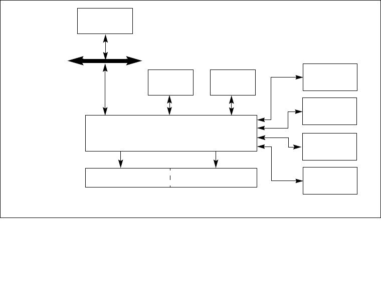
Vol. 3A 10-1
CHAPTER 10
MEMORY CACHE CONTROL
This chapter describes the IA-32 architecture’s memory cache and cache control mechanisms, the
TLBs, and the store buffer. It also describes the memory type range registers (MTRRs) found in
the P6 family processors and how they are used to control caching of physical memory locations.
10.1 INTERNAL CACHES, TLBS, AND BUFFERS
The IA-32 architecture supports caches, translation look aside buffers (TLBs), and a store buffer
for temporary on-chip (and external) storage of instructions and data. (Figure 10-1 shows the
arrangement of caches, TLBs, and the store buffer for the Pentium 4 and Intel Xeon processors.)
Table 10-1 shows the characteristics of these caches and buffers for the Pentium 4, Intel Xeon,
P6 family, and Pentium processors. The sizes and characteristics of these units are machine
specific and may change in future versions of the processor. The CPUID instruction returns
the sizes and characteristics of the caches and buffers for the processor on which the instruction
is executed (see “CPUID—CPU Identification” in Chapter 3, “Instruction Set Reference, A-M,”
of the IA-32 Intel® Architecture Software Developer’s Manual, Volume 2A).
Figure 10-1. Cache Structure of the Pentium 4 and Intel Xeon Processors
Trace Cache
Instruction Decoder
Bus Interface Unit
System Bus
Data Cache
Unit (L1)
(External)
Physical
Memory
Store Buffer
Data TLBs
L2 Cache
Instruction
TLBs
L3 Cache†
† Intel Xeon processors only

10-2 Vol. 3A
MEMORY CACHE CONTROL
Table 10-1. Characteristics of the Caches, TLBs, Store Buffer, and
Write Combining Buffer in IA-32 Processors
Cache or Buffer Characteristics
Trace Cache1- Pentium 4 and Intel Xeon processors: 12 Kμops, 8-way set associative.
- Pentium M processor: not implemented.
- P6 family and Pentium processors: not implemented.
L1 Instruction Cache - Pentium 4 and Intel Xeon processors: not implemented.
- Pentium M processor: 32-KByte, 8-way set associative.
- P6 family and Pentium processors: 8- or 16-KByte, 4-way set associative,
32-byte cache line size; 2-way set associative for earlier Pentium processors.
L1 Data Cache - Pentium 4 and Intel Xeon processors: 8-KByte, 4-way set associative, 64-byte
cache line size.
- Pentium 4 and Intel Xeon processors: 16-KByte, 8-way set associative, 64-byte
cache line size.
- Pentium M processor: 32-KByte, 8-way set associative, 64-byte cache line size.
- P6 family processors: 16-KByte, 4-way set associative, 32-byte cache line size;
8-KBytes, 2-way set associative for earlier P6 family processors.
- Pentium processors: 16-KByte, 4-way set associative, 32-byte cache line size;
8-KByte, 2-way set associative for earlier Pentium processors.
L2 Unified Cache - Pentium 4 and Intel Xeon processors: 256, 512, 1024, or 2048-KByte, 8-way set
associative, 64-byte cache line size, 128-byte sector size.
- Pentium M processor: 1 or 2-MByte, 8-way set associative, 64-byte cache line
size.
- P6 family processors: 128-KByte, 256-KByte, 512-KByte, 1-MByte, or 2-MByte,
4-way set associative, 32-byte cache line size.
- Pentium processor (external optional): System specific, typically 256- or
512-KByte, 4-way set associative, 32-byte cache line size.
L3 Unified Cache - Intel Xeon processors: 512-KByte, 1-MByte, 2-MByte, or 4-MByte, 8-way set
associative, 64-byte cache line size, 128-byte sector size.
Instruction TLB
(4-KByte Pages) - Pentium 4 and Intel Xeon processors: 128 entries, 4-way set associative.
- Pentium M processor: 128 entries, 4-way set associative.
- P6 family processors: 32 entries, 4-way set associative.
- Pentium processor: 32 entries, 4-way set associative; fully set associative for
Pentium processors with MMX technology.
Data TLB (4-KByte
Pages) - Pentium 4 and Intel Xeon processors: 64 entries, fully set associative; shared
with large page data TLBs.
- Pentium M processor: 128 entries, 4-way set associative.
- Pentium and P6 family processors: 64 entries, 4-way set associative; fully set.
associative for Pentium processors with MMX technology.
Instruction TLB
(Large Pages) - Pentium 4 and Intel Xeon processors: large pages are fragmented.
- Pentium M processor: 2 entries, fully associative.
- P6 family processors: 2 entries, fully associative.
- Pentium processor: Uses same TLB as used for 4-KByte pages.
Data TLB (Large
Pages) - Pentium 4 and Intel Xeon processors: 64 entries, fully set associative; shared
with small page data TLBs.
- Pentium M processor: 8 entries, fully associative.
- P6 family processors: 8 entries, 4-way set associative.
- Pentium processor: 8 entries, 4-way set associative; uses same TLB as used for
4-KByte pages in Pentium processors with MMX technology.

Vol. 3A 10-3
MEMORY CACHE CONTROL
The IA-32 processors implement four types of caches: the trace cache, the level 1 (L1) cache,
the level 2 (L2) cache, and the level 3 (L3) cache (see Figure 10-1). The uses of these caches
differs from the Pentium 4, Intel Xeon, and P6 family processors, as follows:
•Pentium 4 and Intel Xeon processors — The trace cache caches decoded instructions
(μops) from the instruction decoder, and the L1 cache contains only data. The L2 and L3
caches are unified data and instruction caches that are located on the processor chip. (The
L3 cache is only implemented on Intel Xeon processors.)
•P6 family processors — The L1 cache is divided into two sections: one dedicated to
caching IA-32 architecture instructions (pre-decoded instructions) and one to caching data.
The L2 cache is a unified data and instruction cache that is located on the processor chip.
The P6 family processors do not implement a trace cache.
•Pentium processors — The L1 cache has the same structure as on the P6 family
processors (and a trace cache is not implemented). The L2 cache is a unified data and
instruction cache that is external to the processor chip on earlier Pentium processors and
implemented on the processor chip in later Pentium processors. For Pentium processors
where the L2 cache is external to the processor, access to the cache is through the system
bus.
The cache lines for the L1 and L2 caches in the Pentium 4 and the L1, L2, and L3 caches in the
Intel Xeon processors are 64 bytes wide. The processor always reads a cache line from system
memory beginning on a 64-byte boundary. (A 64-byte aligned cache line begins at an address
with its 6 least-significant bits clear.) A cache line can be filled from memory with a 8-transfer
burst transaction. The caches do not support partially-filled cache lines, so caching even a single
doubleword requires caching an entire line.
The L1 and L2 cache lines in the P6 family and Pentium processors are 32 bytes wide, with
cache line reads from system memory beginning on a 32-byte boundary (5 least-significant bits
of a memory address clear.) A cache line can be filled from memory with a 4-transfer burst trans-
action. Partially-filled cache lines are not supported.
Store Buffer - Pentium 4 and Intel Xeon processors: 24 entries.
- Pentium M processor: 16 entries.
- P6 family processors: 12 entries.
- Pentium processor: 2 buffers, 1 entry each (Pentium processors with MMX
technology have 4 buffers for 4 entries).
Write Combining
(WC) Buffer - Pentium 4 and Intel Xeon processors: 6 or 8 entries.
- Pentium M processor: 6 entries.
- P6 family processors: 4 entries.
NOTES:
1 Introduced to the IA-32 architecture in the Pentium 4 and Intel Xeon processors.
Table 10-1. Characteristics of the Caches, TLBs, Store Buffer, and
Write Combining Buffer in IA-32 Processors (Contd.)
Cache or Buffer Characteristics

10-4 Vol. 3A
MEMORY CACHE CONTROL
The trace cache in the Pentium 4 and Intel Xeon processors is an integral part of the Intel
NetBurst microarchitecture and is available in all execution modes: protected mode, system
management mode (SMM), and real-address mode. The L1,L2, and L3 caches are also available
in all execution modes; however, use of them must be handled carefully in SMM (see Section
24.4.2, “SMRAM Caching”).
The TLBs store the most recently used page-directory and page-table entries. They speed up
memory accesses when paging is enabled by reducing the number of memory accesses that are
required to read the page tables stored in system memory. The TLBs are divided into four
groups: instruction TLBs for 4-KByte pages, data TLBs for 4-KByte pages; instruction TLBs
for large pages (2-MByte or 4-MByte pages), and data TLBs for large pages. The TLBs are
normally active only in protected mode with paging enabled. When paging is disabled or the
processor is in real-address mode, the TLBs maintain their contents until explicitly or implicitly
flushed (see Section 10.9, “Invalidating the Translation Lookaside Buffers (TLBs)”).
The store buffer is associated with the processors instruction execution units. It allows writes to
system memory and/or the internal caches to be saved and in some cases combined to optimize
the processor’s bus accesses. The store buffer is always enabled in all execution modes.
The processor’s caches are for the most part transparent to software. When enabled, instructions
and data flow through these caches without the need for explicit software control. However,
knowledge of the behavior of these caches may be useful in optimizing software performance.
For example, knowledge of cache dimensions and replacement algorithms gives an indication
of how large of a data structure can be operated on at once without causing cache thrashing.
In multiprocessor systems, maintenance of cache consistency may, in rare circumstances,
require intervention by system software. For these rare cases, the processor provides privileged
cache control instructions for use in flushing caches and forcing memory ordering.
The Pentium III, Pentium 4, and Intel Xeon processors introduced several instructions that soft-
ware can use to improve the performance of the L1, L2, and L3 caches, including the
PREFETCHh and CLFLUSH instructions and the non-temporal move instructions (MOVNTI,
MOVNTQ, MOVNTDQ, MOVNTPS, and MOVNTPD). The use of these instructions are
discussed in Section 10.5.5, “Cache Management Instructions.”
10.2 CACHING TERMINOLOGY
The IA-32 architecture (beginning with the Pentium processor) uses the MESI (modified, exclu-
sive, shared, invalid) cache protocol to maintain consistency with internal caches and caches in
other processors (see Section 10.4, “Cache Control Protocol”).
When the processor recognizes that an operand being read from memory is cacheable, the
processor reads an entire cache line into the appropriate cache (L1, L2, L3, or all). This operation
is called a cache line fill. If the memory location containing that operand is still cached the next
time the processor attempts to access the operand, the processor can read the operand from the
cache instead of going back to memory. This operation is called a cache hit.

Vol. 3A 10-5
MEMORY CACHE CONTROL
When the processor attempts to write an operand to a cacheable area of memory, it first checks
if a cache line for that memory location exists in the cache. If a valid cache line does exist, the
processor (depending on the write policy currently in force) can write the operand into the cache
instead of writing it out to system memory. This operation is called a write hit. If a write misses
the cache (that is, a valid cache line is not present for area of memory being written to), the
processor performs a cache line fill, write allocation. Then it writes the operand into the cache
line and (depending on the write policy currently in force) can also write it out to memory. If the
operand is to be written out to memory, it is written first into the store buffer, and then written
from the store buffer to memory when the system bus is available. (Note that for the Pentium
processor, write misses do not result in a cache line fill; they always result in a write to memory.
For this processor, only read misses result in cache line fills.)
When operating in an MP system, IA-32 processors (beginning with the Intel486 processor)
have the ability to snoop other processor’s accesses to system memory and to their internal
caches. They use this snooping ability to keep their internal caches consistent both with system
memory and with the caches in other processors on the bus. For example, in the Pentium and P6
family processors, if through snooping one processor detects that another processor intends to
write to a memory location that it currently has cached in shared state, the snooping processor
will invalidate its cache line forcing it to perform a cache line fill the next time it accesses the
same memory location.
Beginning with the P6 family processors, if a processor detects (through snooping) that another
processor is trying to access a memory location that it has modified in its cache, but has not yet
written back to system memory, the snooping processor will signal the other processor (by
means of the HITM# signal) that the cache line is held in modified state and will preform an
implicit write-back of the modified data. The implicit write-back is transferred directly to the
initial requesting processor and snooped by the memory controller to assure that system memory
has been updated. Here, the processor with the valid data may pass the data to the other proces-
sors without actually writing it to system memory; however, it is the responsibility of the
memory controller to snoop this operation and update memory.
10.3 METHODS OF CACHING AVAILABLE
The processor allows any area of system memory to be cached in the L1, L2, and L3 caches. In
individual pages or regions of system memory, it allows the type of caching (also called
memory type) to be specified (see Section 10.5). Memory types currently defined for the IA-32
architecture are as follows (see Table 10-2):
•Strong Uncacheable (UC) —System memory locations are not cached. All reads and
writes appear on the system bus and are executed in program order without reordering. No
speculative memory accesses, page-table walks, or prefetches of speculated branch targets
are made. This type of cache-control is useful for memory-mapped I/O devices. When
used with normal RAM, it greatly reduces processor performance.

10-6 Vol. 3A
MEMORY CACHE CONTROL
NOTE
The behavior of FP and SSE/SSE2 operations on operands in UC memory is
implementation dependent. In some implementations, accesses to UC
memory may occur more than once. To ensure predictable behavior, use loads
and stores of general purpose registers to access UC memory that may have
read or write side effects.
•Uncacheable (UC-) — Has same characteristics as the strong uncacheable (UC) memory
type, except that this memory type can be overridden by programming the MTRRs for the
WC memory type. This memory type is available in the Pentium 4, Intel Xeon, and
Pentium III processors and can only be selected through the PAT.
•Write Combining (WC) — System memory locations are not cached (as with
uncacheable memory) and coherency is not enforced by the processor’s bus coherency
protocol. Speculative reads are allowed. Writes may be delayed and combined in the write
combining buffer (WC buffer) to reduce memory accesses. If the WC buffer is partially
filled, the writes may be delayed until the next occurrence of a serializing event; such as,
an SFENCE or MFENCE instruction, CPUID execution, a read or write to uncached
memory, an interrupt occurrence, or a LOCK instruction execution. This type of cache-
control is appropriate for video frame buffers, where the order of writes is unimportant as
long as the writes update memory so they can be seen on the graphics display. See Section
10.3.1, “Buffering of Write Combining Memory Locations,” for more information about
caching the WC memory type. This memory type is available in the Pentium Pro and
Pentium II processors by programming the MTRRs or in the Pentium III, Pentium 4, and
Intel Xeon processors by programming the MTRRs or by selecting it through the PAT.
•Write-through (WT) — Writes and reads to and from system memory are cached. Reads
come from cache lines on cache hits; read misses cause cache fills. Speculative reads are
allowed. All writes are written to a cache line (when possible) and through to system
Table 10-2. Memory Types and Their Properties
Memory Type and
Mnemonic Cacheable Writeback
Cacheable Allows
Speculative
Reads
Memory Ordering Model
Strong Uncacheable
(UC) No No No Strong Ordering
Uncacheable (UC-) No No No Strong Ordering. Can only be
selected through the PAT. Can
be overridden by WC in MTRRs.
Write Combining (WC) No No Yes Weak Ordering. Available by
programming MTRRs or by
selecting it through the PAT.
Write Through (WT) Yes No Yes Speculative Processor Ordering.
Write Back (WB) Yes Yes Yes Speculative Processor Ordering.
Write Protected (WP) Yes for
reads; no for
writes
No Yes Speculative Processor Ordering.
Available by programming
MTRRs.

Vol. 3A 10-7
MEMORY CACHE CONTROL
memory. When writing through to memory, invalid cache lines are never filled, and valid
cache lines are either filled or invalidated. Write combining is allowed. This type of cache-
control is appropriate for frame buffers or when there are devices on the system bus that
access system memory, but do not perform snooping of memory accesses. It enforces
coherency between caches in the processors and system memory.
•Write-back (WB) — Writes and reads to and from system memory are cached. Reads
come from cache lines on cache hits; read misses cause cache fills. Speculative reads are
allowed. Write misses cause cache line fills (in the Pentium 4, Intel Xeon, and P6 family
processors), and writes are performed entirely in the cache, when possible. Write
combining is allowed. The write-back memory type reduces bus traffic by eliminating
many unnecessary writes to system memory. Writes to a cache line are not immediately
forwarded to system memory; instead, they are accumulated in the cache. The modified
cache lines are written to system memory later, when a write-back operation is performed.
Write-back operations are triggered when cache lines need to be deallocated, such as when
new cache lines are being allocated in a cache that is already full. They also are triggered
by the mechanisms used to maintain cache consistency. This type of cache-control
provides the best performance, but it requires that all devices that access system memory
on the system bus be able to snoop memory accesses to insure system memory and cache
coherency.
•Write protected (WP) — Reads come from cache lines when possible, and read misses
cause cache fills. Writes are propagated to the system bus and cause corresponding cache
lines on all processors on the bus to be invalidated. Speculative reads are allowed. This
memory type is available in the Pentium 4, Intel Xeon, and P6 family processors by
programming the MTRRs (see Table 10-6).
Table 10-3 shows which of these caching methods are available in the Pentium, P6 Family,
Pentium 4, and Intel Xeon processors.
Table 10-3. Methods of Caching Available in Pentium 4, Intel Xeon, P6 Family,
and Pentium Processors
Memory Type Pentium 4 and Intel
Xeon Processors P6 Family Processors Pentium Processor
Strong Uncacheable (UC) Yes Yes Yes
Uncacheable (UC-) Yes Yes* No
Write Combining (WC) Yes Yes No
Write Through (WT) Yes Yes Yes
Write Back (WB) Yes Yes Yes
Write Protected (WP) Yes Yes No
NOTE:
* Introduced in the Pentium III processor; not available in the Pentium Pro or Pentium II processors

10-8 Vol. 3A
MEMORY CACHE CONTROL
10.3.1 Buffering of Write Combining Memory Locations
Writes to the WC memory type are not cached in the typical sense of the word cached. They are
retained in an internal write combining buffer (WC buffer) that is separate from the internal L1,
L2, and L3 caches and the store buffer. The WC buffer is not snooped and thus does not provide
data coherency. Buffering of writes to WC memory is done to allow software a small window
of time to supply more modified data to the WC buffer while remaining as non-intrusive to soft-
ware as possible. The buffering of writes to WC memory also causes data to be collapsed; that
is, multiple writes to the same memory location will leave the last data written in the location
and the other writes will be lost.
The size and structure of the WC buffer is not architecturally defined. For the Pentium 4 and
Intel Xeon processors, the WC buffer is made up of several 64-byte WC buffers. For the P6
family processors, the WC buffer is made up of several 32-byte WC buffers.
When software begins writing to WC memory, the processor begins filling the WC buffers one
at a time. When one or more WC buffers has been filled, the processor has the option of evicting
the buffers to system memory. The protocol for evicting the WC buffers is implementation
dependent and should not be relied on by software for system memory coherency. When using
the WC memory type, software must be sensitive to the fact that the writing of data to system
memory is being delayed and must deliberately empty the WC buffers when system memory
coherency is required.
Once the processor has started to evict data from the WC buffer into system memory, it will
make a bus-transaction style decision based on how much of the buffer contains valid data. If
the buffer is full (for example, all bytes are valid) the processor will execute a burst-write trans-
action on the bus that will result in all 32 bytes (P6 family processors) or 64 bytes (Pentium 4
and Intel Xeon processor) being transmitted on the data bus in a single burst transaction. If one
or more of the WC buffer’s bytes are invalid (for example, have not been written by software)
then the processor will transmit the data to memory using “partial write” transactions (one chunk
at a time, where a “chunk” is 8 bytes).
This will result in a maximum of 4 partial write transactions (for P6 family processors) or 8
partial write transactions (for the Pentium 4 and Intel Xeon processors) for one WC buffer of
data sent to memory.
The WC memory type is weakly ordered by definition. Once the eviction of a WC buffer has
started, the data is subject to the weak ordering semantics of its definition. Ordering is not main-
tained between the successive allocation/deallocation of WC buffers (for example, writes to WC
buffer 1 followed by writes to WC buffer 2 may appear as buffer 2 followed by buffer 1 on the
system bus). When a WC buffer is evicted to memory as partial writes there is no guaranteed
ordering between successive partial writes (for example, a partial write for chunk 2 may appear
on the bus before the partial write for chunk 1 or vice versa).

Vol. 3A 10-9
MEMORY CACHE CONTROL
The only elements of WC propagation to the system bus that are guaranteed are those provided
by transaction atomicity. For example, with a P6 family processor, a completely full WC buffer
will always be propagated as a single 32-bit burst transaction using any chunk order. In a WC
buffer eviction where the data will be evicted as partials, all data contained in the same chunk
(0 mod 8 aligned) will be propagated simultaneously. Likewise, with a Pentium 4 or Intel Xeon
processor, a full WC buffer will always be propagated as a single burst transactions, using any
chunk order within a transaction. For partial buffer propagations, all data contained in the same
chunk will be propagated simultaneously.
10.3.2 Choosing a Memory Type
The simplest system memory model does not use memory-mapped I/O with read or write side
effects, does not include a frame buffer, and uses the write-back memory type for all memory.
An I/O agent can perform direct memory access (DMA) to write-back memory and the cache
protocol maintains cache coherency.
A system can use strong uncacheable memory for other memory-mapped I/O, and should
always use strong uncacheable memory for memory-mapped I/O with read side effects.
Dual-ported memory can be considered a write side effect, making relatively prompt writes
desirable, because those writes cannot be observed at the other port until they reach the memory
agent. A system can use strong uncacheable, uncacheable, write-through, or write-combining
memory for frame buffers or dual-ported memory that contains pixel values displayed on a
screen. Frame buffer memory is typically large (a few megabytes) and is usually written more
than it is read by the processor. Using strong uncacheable memory for a frame buffer generates
very large amounts of bus traffic, because operations on the entire buffer are implemented using
partial writes rather than line writes. Using write-through memory for a frame buffer can
displace almost all other useful cached lines in the processor's L2 and L3 caches and L1 data
cache. Therefore, systems should use write-combining memory for frame buffers whenever
possible.
Software can use page-level cache control, to assign appropriate effective memory types when
software will not access data structures in ways that benefit from write-back caching. For
example, software may read a large data structure once and not access the structure again until
the structure is rewritten by another agent. Such a large data structure should be marked as
uncacheable, or reading it will evict cached lines that the processor will be referencing again.
A similar example would be a write-only data structure that is written to (to export the data to
another agent), but never read by software. Such a structure can be marked as uncacheable,
because software never reads the values that it writes (though as uncacheable memory, it will be
written using partial writes, while as write-back memory, it will be written using line writes,
which may not occur until the other agent reads the structure and triggers implicit write-backs).
On the Pentium III, Pentium 4, and Intel Xeon processors, new instructions are provided that
give software greater control over the caching, prefetching, and the write-back characteristics of
data. These instructions allow software to use weakly ordered or processor ordered memory
types to improve processor performance, but when necessary to force strong ordering on
memory reads and/or writes. They also allow software greater control over the caching of data.

10-10 Vol. 3A
MEMORY CACHE CONTROL
For a description of these instructions and there intended use, see Section 10.5.5, “Cache
Management Instructions.”
10.4 CACHE CONTROL PROTOCOL
The following section describes the cache control protocol currently defined for the IA-32 archi-
tecture. This protocol is used by the Pentium 4, Intel Xeon, P6 family, and Pentium processors.
In the L1 data cache and in the L2 and L3 unified caches, the MESI (modified, exclusive, shared,
invalid) cache protocol maintains consistency with caches of other processors. The L1 data
cache and the L2 and L3 unified caches have two MESI status flags per cache line. Each line
can thus be marked as being in one of the states defined in Table 10-4. In general, the operation
of the MESI protocol is transparent to programs.
The L1 instruction cache in P6 family processors implements only the “SI” part of the MESI
protocol, because the instruction cache is not writable. The instruction cache monitors changes
in the data cache to maintain consistency between the caches when instructions are modified.
See Section 10.6, “Self-Modifying Code,” for more information on the implications of caching
instructions.
10.5 CACHE CONTROL
The IA-32 architecture provides a variety of mechanisms for controlling the caching of data and
instructions and for controlling the ordering of reads and writes between the processor, the
caches, and memory. These mechanisms can be divided into two groups:
•Cache control registers and bits — The IA-32 architecture defines several dedicated
registers and various bits within control registers and page- and directory-table entries that
control the caching system memory locations in the L1, L2, and L3 caches. These
mechanisms control the caching of virtual memory pages and of regions of physical
memory.
Table 10-4. MESI Cache Line States
Cache Line State M (Modified) E (Exclusive) S (Shared) I (Invalid)
This cache line is valid? Yes Yes Yes No
The memory copy is… Out of date Valid Valid —
Copies exist in caches of
other processors? No No Maybe Maybe
A write to this line … Does not go to
the system bus. Does not go to
the system bus. Causes the
processor to
gain exclusive
ownership of the
line.
Goes directly to
the system bus.

Vol. 3A 10-11
MEMORY CACHE CONTROL
•Cache control and memory ordering instructions — The IA-32 architecture provides
several instructions that control the caching of data, the ordering of memory reads and
writes, and the prefetching of data. These instructions allow software to control the
caching of specific data structures, to control memory coherency for specific locations in
memory, and to force strong memory ordering at specific locations in a program.
The following sections describe these two groups of cache control mechanisms.
10.5.1 Cache Control Registers and Bits
The current IA-32 architecture provides the following cache-control registers and bits for use in
enabling and/or restricting caching to various pages or regions in memory (see Figure 10-2):
•CD flag, bit 30 of control register CR0 — Controls caching of system memory locations
(see Section 2.5, “Control Registers”). If the CD flag is clear, caching is enabled for the
whole of system memory, but may be restricted for individual pages or regions of memory
by other cache-control mechanisms. When the CD flag is set, caching is restricted in the
processor’s caches (cache hierarchy) for the Pentium 4, Intel Xeon, and P6 family
processors and prevented for the Pentium processor (see note below). With the CD flag set,
however, the caches will still respond to snoop traffic. Caches should be explicitly flushed
to insure memory coherency. For highest processor performance, both the CD and the NW
flags in control register CR0 should be cleared. Table 10-5 shows the interaction of the CD
and NW flags.
The effect of setting the CD flag is somewhat different for the Pentium 4, Intel Xeon,
and P6 family processors than for the Pentium processor (see Table 10-5). To insure
memory coherency after the CD flag is set, the caches should be explicitly flushed (see
Section 10.5.3, “Preventing Caching”). Setting the CD flag for the Pentium 4, Intel
Xeon, and P6 family processors modifies cache line fill and update behaviour. Also for
the Pentium 4, Intel Xeon, and P6 family processors, setting the CD flag does not force
strict ordering of memory accesses unless the MTRRs are disabled and/or all memory is
referenced as uncached (see Section 7.2.4, “Strengthening or Weakening the Memory
Ordering Model”).
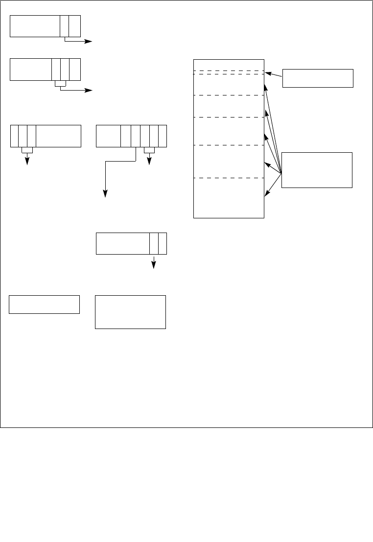
10-12 Vol. 3A
MEMORY CACHE CONTROL
Figure 10-2. Cache-Control Registers and Bits Available in IA-32 Processors
Page-Directory or
Page-Table Entry
TLBs
MTRRs3
Physical Memory
0
FFFFFFFFH2
control overall caching
of system memory
CD and NW Flags PCD and PWT flags
control page-level
caching
G flag controls page-
level flushing of TLBs
MTRRs control caching
of selected regions of
physical memory
P
C
D
CR3
Control caching of
page directory
P
W
T
C
D
CR0
N
W
Store Buffer
P
C
D
P
W
T
G1
CR4
Enables global pages
P
G
E
designated with G flag
1. G flag only available in Pentium 4, Intel Xeon, and P6 family
3. MTRRs available only in Pentium 4 and P6 family processors;
similar control available in Pentium processor with the KEN#
and WB/WT# pins.
2. The maximum physical address size is reported by CPUID leaf
function 80000008H. The maximum physical address size of
PAT4
PAT controls caching
of virtual memory
pages
4. PAT available only in Pentium III and Pentium 4 processors.
P4
A
T
processors.
IA32_MISC_ENABLE MSR
3rd Level
Cache Disable
FFFFFFFFFH applies only If 36-bit physical addressing is used.

Vol. 3A 10-13
MEMORY CACHE CONTROL
Table 10-5. Cache Operating Modes
CD NW Caching and Read/Write Policy L1 L2/L31
0 0 Normal Cache Mode. Highest performance cache operation.
- Read hits access the cache; read misses may cause replacement.
- Write hits update the cache.
- Only writes to shared lines and write misses update system memory.
- Write misses cause cache line fills.
- Write hits can change shared lines to modified under control of the
MTRRs and with associated read invalidation cycle.
- (Pentium processor only.) Write misses do not cause cache line fills.
- (Pentium processor only.) Write hits can change shared lines to
exclusive under control of WB/WT#.
- Invalidation is allowed.
- External snoop traffic is supported.
Yes
Yes
Yes
Yes
Yes
Yes
Yes
Yes
Yes
Yes
Yes
Yes
Yes
Yes
Yes
Yes
0 1 Invalid setting.
Generates a general-protection exception (#GP) with an error code of 0. NA NA
1 0 No-fill Cache Mode. Memory coherency is maintained.
- (Pentium 4 and Intel Xeon processors.) State of processor after a power
up or reset.
- Read hits access the cache; read misses do not cause replacement
(see Pentium 4 and Intel Xeon processors reference below).
- Write hits update the cache.
- Only writes to shared lines and write misses update system memory.
- Write misses access memory.
- Write hits can change shared lines to exclusive under control of the
MTRRs and with associated read invalidation cycle.
- (Pentium processor only.) Write hits can change shared lines to
exclusive under control of the WB/WT#.
- (Pentium 4, Intel Xeon, and P6 family processors only.) Strict memory
ordering is not enforced unless the MTRRs are disabled and/or all
memory is referenced as uncached (see Section 7.2.4., “Strengthening
or Weakening the Memory Ordering Model”).
- Invalidation is allowed.
- External snoop traffic is supported.
Yes
Yes
Yes
Yes
Yes
Yes
Yes
Yes
Yes
Yes
Yes
Yes
Yes
Yes
Yes
Yes
Yes
Yes
Yes
1 1 Memory coherency is not maintained.2
- (P6 family and Pentium processors.) State of the processor after a
power up or reset.
- Read hits access the cache; read misses do not cause replacement.
- Write hits update the cache and change exclusive lines to modified.
- Shared lines remain shared after write hit.
- Write misses access memory.
- Invalidation is inhibited when snooping; but is allowed with INVD and
WBINVD instructions.
- External snoop traffic is supported.
Yes
Yes
Yes
Yes
Yes
Yes
No
Yes
Yes
Yes
Yes
Yes
Yes
Yes
NOTES:
1. The L2/L3 column in this table is definitive for the Pentium 4, Intel Xeon, and P6 family processors. It is
intended to represent what could be implemented in a system based on a Pentium processor with an
external, platform specific, write-back L2 cache.
2. The Pentium 4 and Intel Xeon processors do not support this mode; setting the CD and NW bits to 1
selects the no-fill cache mode.

10-14 Vol. 3A
MEMORY CACHE CONTROL
•NW flag, bit 29 of control register CR0 — Controls the write policy for system memory
locations (see Section 2.5, “Control Registers”). If the NW and CD flags are clear, write-
back is enabled for the whole of system memory, but may be restricted for individual pages
or regions of memory by other cache-control mechanisms. Table 10-5 shows how the other
combinations of CD and NW flags affects caching.
NOTES
For the Pentium 4 and Intel Xeon processors, the NW flag is a don’t care flag;
that is, when the CD flag is set, the processor uses the no-fill cache mode,
regardless of the setting of the NW flag.
For the Pentium processor, when the L1 cache is disabled (the CD and NW
flags in control register CR0 are set), external snoops are accepted in DP
(dual-processor) systems and inhibited in uniprocessor systems.
When snoops are inhibited, address parity is not checked and APCHK# is not
asserted for a corrupt address; however, when snoops are accepted, address
parity is checked and APCHK# is asserted for corrupt addresses.
•PCD flag in the page-directory and page-table entries — Controls caching for
individual page tables and pages, respectively (see Section 3.7.6, “Page-Directory and
Page-Table Entries”). This flag only has effect when paging is enabled and the CD flag in
control register CR0 is clear. The PCD flag enables caching of the page table or page when
clear and prevents caching when set.
•PWT flag in the page-directory and page-table entries — Controls the write policy for
individual page tables and pages, respectively (see Section 3.7.6, “Page-Directory and
Page-Table Entries”). This flag only has effect when paging is enabled and the NW flag in
control register CR0 is clear. The PWT flag enables write-back caching of the page table or
page when clear and write-through caching when set.
•PCD and PWT flags in control register CR3 — Control the global caching and write
policy for the page directory (see Section 2.5, “Control Registers”). The PCD flag enables
caching of the page directory when clear and prevents caching when set. The PWT flag
enables write-back caching of the page directory when clear and write-through caching
when set. These flags do not affect the caching and write policy for individual page tables.
These flags only have effect when paging is enabled and the CD flag in control register
CR0 is clear.
•G (global) flag in the page-directory and page-table entries (introduced to the IA-32
architecture in the P6 family processors) — Controls the flushing of TLB entries for
individual pages. See Section 3.12, “Translation Lookaside Buffers (TLBs),” for more
information about this flag.
•PGE (page global enable) flag in control register CR4 — Enables the establishment of
global pages with the G flag. See Section 3.12, “Translation Lookaside Buffers (TLBs),”
for more information about this flag.

Vol. 3A 10-15
MEMORY CACHE CONTROL
•Memory type range registers (MTRRs) (introduced in P6 family processors) —
Control the type of caching used in specific regions of physical memory. Any of the
caching types described in Section 10.3, “Methods of Caching Available,” can be selected.
See Section 10.11, “Memory Type Range Registers (MTRRs),” for a detailed description
of the MTRRs.
•Page Attribute Table (PAT) MSR (introduced in the Pentium III processor) — Extends
the memory typing capabilities of the processor to permit memory types to be assigned on
a page-by-page basis (see Section 10.12, “Page Attribute Table (PAT)”).
•Third-Level Cache Disable flag, bit 6 of the IA32_MISC_ENABLE MSR (introduced
in the Intel Xeon processors) — Allows the L3 cache to be disabled and enabled,
independently of the L1 and L2 caches.
•KEN# and WB/WT# pins (Pentium processor) — Allow external hardware to control
the caching method used for specific areas of memory. They perform similar (but not
identical) functions to the MTRRs in the P6 family processors.
•PCD and PWT pins (Pentium processor) — These pins (which are associated with the
PCD and PWT flags in control register CR3 and in the page-directory and page-table
entries) permit caching in an external L2 cache to be controlled on a page-by-page basis,
consistent with the control exercised on the L1 cache of these processors. The Pentium 4,
Intel Xeon, and P6 family processors do not provide these pins because the L2 cache in
internal to the chip package.
10.5.2 Precedence of Cache Controls
The cache control flags and MTRRs operate hierarchically for restricting caching. That is, if the
CD flag is set, caching is prevented globally (see Table 10-5). If the CD flag is clear, the page-
level cache control flags and/or the MTRRs can be used to restrict caching. If there is an overlap
of page-level and MTRR caching controls, the mechanism that prevents caching has prece-
dence. For example, if an MTRR makes a region of system memory uncachable, a page-level
caching control cannot be used to enable caching for a page in that region. The converse is also
true; that is, if a page-level caching control designates a page as uncachable, an MTRR cannot
be used to make the page cacheable.
In cases where there is a overlap in the assignment of the write-back and write-through caching
policies to a page and a region of memory, the write-through policy takes precedence. The write-
combining policy (which can only be assigned through an MTRR or the PAT) takes precedence
over either write-through or write-back.
The selection of memory types at the page level varies depending on whether PAT is being used
to select memory types for pages, as described in the following sections.
Third-level cache disable flag (bit 6 of the IA32_MISC_ENABLE MSR) takes precedence over
the CD flag, MTRRs, and PAT for the L3 cache. That is, when the third-level cache disable flag
is set (cache disabled), the other cache controls have no affect on the L3 cache; when the flag is
clear (enabled), the cache controls have the same affect on the L3 cache as they have on the L1
and L2 caches.

10-16 Vol. 3A
MEMORY CACHE CONTROL
10.5.2.1 Selecting Memory Types for Pentium Pro and Pentium II Processors
The Pentium Pro and Pentium II processors do not support the PAT. Here, the effective memory
type for a page is selected with the MTRRs and the PCD and PWT bits in the page-table or page-
directory entry for the page. Table 10-6 describes the mapping of MTRR memory types and
page-level caching attributes to effective memory types, when normal caching is in effect (the
CD and NW flags in control register CR0 are clear). Combinations that appear in gray are imple-
mentation-defined for the Pentium Pro and Pentium II processors. System designers are encour-
aged to avoid these implementation-defined combinations.
When normal caching is in effect, the effective memory type shown in Table 10-6 is determined
using the following rules:
1. If the PCD and PWT attributes for the page are both 0, then the effective memory type is
identical to the MTRR-defined memory type.
2. If the PCD flag is set, then the effective memory type is UC.
3. If the PCD flag is clear and the PWT flag is set, the effective memory type is WT for the
WB memory type and the MTRR-defined memory type for all other memory types.
Table 10-6. Effective Page-Level Memory Type for Pentium Pro and
Pentium II Processors
MTRR Memory Type1PCD Value PWT Value Effective Memory Type
UC X X UC
WC 0 0 WC
0 1 WC
1 0 WC
11 UC
WT 0 X WT
1X UC
WP 0 0 WP
0 1 WP
1 0 WC
11 UC
WB 0 0 WB
01 WT
1X UC
NOTE:
1. These effective memory types also apply to the Pentium 4, Intel Xeon, and Pentium III processors
when the PAT bit is not used (set to 0) in page-table and page-directory entries.

Vol. 3A 10-17
MEMORY CACHE CONTROL
4. Setting the PCD and PWT flags to opposite values is considered model-specific for the WP
and WC memory types and architecturally-defined for the WB, WT, and UC memory
types.
10.5.2.2 Selecting Memory Types for Pentium 4, Intel Xeon,
and Pentium III Processors
The Pentium 4, Intel Xeon, and Pentium III processors use the PAT to select effective page-level
memory types. Here, a memory type for a page is selected by the MTRRs and the value in a PAT
entry that is selected with the PAT, PCD and PWT bits in a page-table or page-directory entry
(see Section 10.12.3, “Selecting a Memory Type from the PAT”). Table 10-7 describes the
mapping of MTRR memory types and PAT entry types to effective memory types, when normal
caching is in effect (the CD and NW flags in control register CR0 are clear). The combinations
shown in gray are implementation-defined for the Pentium 4, Intel Xeon, and Pentium III proces-
sors. System designers are encouraged to avoid the implementation-defined combinations.
Table 10-7. Effective Page-Level Memory Types for Pentium III, Pentium 4,
and Intel Xeon Processors
MTRR Memory Type PAT Entry Value Effective Memory Type
UC UC UC1
UC- UC1
WC WC
WT UC1
WB UC1
WP UC1
WC UC UC2
UC- WC
WC WC
WT UC2,3
WB WC
WP UC2,3
WT UC UC2
UC- UC2
WC WC
WT WT
WB WT
WP WP3

10-18 Vol. 3A
MEMORY CACHE CONTROL
10.5.2.3 Writing Values Across Pages with Different Memory Types
If two adjoining pages in memory have different memory types, and a word or longer operand
is written to a memory location that crosses the page boundary between those two pages, the
operand might be written to memory twice. This action does not present a problem for writes to
actual memory; however, if a device is mapped the memory space assigned to the pages, the
device might malfunction.
10.5.3 Preventing Caching
To disable the L1, L2, and L3 caches after they have been enabled and have received cache fills,
perform the following steps:
1. Enter the no-fill cache mode. (Set the CD flag in control register CR0 to 1 and the NW flag
to 0.
2. Flush all caches using the WBINVD instruction.
WB UC UC2
UC- UC2
WC WC
WT WT
WB WB
WP WP
WP UC UC2
UC- WC3
WC WC
WT WT3
WB WP
WP WP
NOTES:
1. The UC attribute comes from the MTRRs and the processors are not required to snoop their caches
since the data could never have been cached. This attribute is preferred for performance reasons.
2. The UC attribute came from the page-table or page-directory entry and processors are required to check
their caches because the data may be cached due to page aliasing, which is not recommended.
3. These combinations were specified as “undefined” in previous editions of the IA-32 Intel® Architecture
Software Developer’s Manual. However, all processors that support both the PAT and the MTRRs deter-
mine the effective page-level memory types for these combinations as given.
Table 10-7. Effective Page-Level Memory Types for Pentium III, Pentium 4,
and Intel Xeon Processors (Contd.)
MTRR Memory Type PAT Entry Value Effective Memory Type

Vol. 3A 10-19
MEMORY CACHE CONTROL
3. Disable the MTRRs and set the default memory type to uncached or set all MTRRs for the
uncached memory type (see the discussion of the discussion of the TYPE field and the E
flag in Section 10.11.2.1, “IA32_MTRR_DEF_TYPE MSR”).
The caches must be flushed (step 2) after the CD flag is set to insure system memory coherency.
If the caches are not flushed, cache hits on reads will still occur and data will be read from valid
cache lines.
NOTES
Setting the CD flag in control register CR0 modifies the processor’s caching
behaviour as indicated in Table 10-5, but it does not force the effective
memory type for all physical memory to be UC nor does it force strict
memory ordering. To force the UC memory type and strict memory ordering
on all of physical memory, either the MTRRs must all be programmed for the
UC memory type or they must be disabled.
For the Pentium 4 and Intel Xeon processors, after the sequence of steps
given above has been executed, the cache lines containing the code between
the end of the WBINVD instruction and before the MTRRS have actually
been disabled may be retained in the cache hierarchy. Here, to remove code
from the cache completely, a second WBINVD instruction must be executed
after the MTRRs have been disabled.
10.5.4 Disabling and Enabling the L3 Cache
Third-level cache disable flag (bit 6 of the IA32_MISC_ENABLE MSR) allows the L3 cache
to be disabled and enabled, independently of the L1 and L2 caches. Prior to using this control to
disable or enable the L3 cache, software should disable and flush all the processor caches, as
described earlier in Section 10.5.3, “Preventing Caching,” to prevent of loss of information
stored in the L3 cache. After the L3 cache has been disabled or enabled, caching for the whole
processor can be restored.
10.5.5 Cache Management Instructions
The IA-32 architecture provide several instructions for managing the L1, L2, and L3 caches. The
INVD, WBINVD, and WBINVD instructions are system instructions that operate on the L1, L2,
and L3 caches as a whole. The PREFETCHh and CLFLUSH instructions and the non-temporal
move instructions (MOVNTI, MOVNTQ, MOVNTDQ, MOVNTPS, and MOVNTPD), which
were introduced in SSE/SSE2 extensions, offer more granular control over caching.
The INVD and WBINVD instructions are used to invalidate the contents of the L1, L2, and L3
caches. The INVD instruction invalidates all internal cache entries, then generates a special-
function bus cycle that indicates that external caches also should be invalidated. The INVD
instruction should be used with care. It does not force a write-back of modified cache lines;
therefore, data stored in the caches and not written back to system memory will be lost. Unless
there is a specific requirement or benefit to invalidating the caches without writing back the

10-20 Vol. 3A
MEMORY CACHE CONTROL
modified lines (such as, during testing or fault recovery where cache coherency with main
memory is not a concern), software should use the WBINVD instruction.
The WBINVD instruction first writes back any modified lines in all the internal caches, then
invalidates the contents of both the L1, L2, and L3 caches. It ensures that cache coherency with
main memory is maintained regardless of the write policy in effect (that is, write-through or
write-back). Following this operation, the WBINVD instruction generates one (P6 family
processors) or two (Pentium and Intel486 processors) special-function bus cycles to indicate to
external cache controllers that write-back of modified data followed by invalidation of external
caches should occur.
The PREFETCHh instructions allow a program to suggest to the processor that a cache line from
a specified location in system memory be prefetched into the cache hierarchy (see Section 10.8,
“Explicit Caching”).
The CLFLUSH instruction allow selected cache lines to be flushed from memory. This instruc-
tion give a program the ability to explicitly free up cache space, when it is known that cached
section of system memory will not be accessed in the near future.
The non-temporal move instructions (MOVNTI, MOVNTQ, MOVNTDQ, MOVNTPS, and
MOVNTPD) allow data to be moved from the processor’s registers directly into system memory
without being also written into the L1, L2, and/or L3 caches. These instructions can be used to
prevent cache pollution when operating on data that is going to be modified only once before
being stored back into system memory. These instructions operate on data in the general-
purpose, MMX, and XMM registers.
10.5.6 L1 Data Cache Context Mode
L1 data cache context mode is a feature of IA-32 processors that support Hyper-Threading Tech-
nology. When CPUID.1:ECX[bit 10] = 1, the processor supports setting L1 data cache context
mode using the L1 data cache context mode flag ( IA32_MISC_ENABLE[bit 24] ). Selectable
modes are adaptive mode (default) and shared mode.
The BIOS is responsible for configuring the L1 data cache context mode.

Vol. 3A 10-21
MEMORY CACHE CONTROL
10.5.6.1 Adaptive Mode
Adaptive mode facilitates L1 data cache sharing between logical processors. When running in
adaptive mode, the L1 data cache is shared across logical processors in the same core if:
•CR3 control registers for logical processors sharing the cache are identical.
•The same paging mode is used by logical processors sharing the cache.
In this situation, the entire L1 data cache is available to each logical processor (instead of being
competitively shared).
If CR3 values are different for the logical processors sharing an L1 data cache or the logical
processors use different paging modes, processors compete for cache resources. This reduces
the effective size of the cache for each logical processor. Aliasing of the cache is not allowed
(which prevents data thrashing).
10.5.6.2 Shared Mode
In shared mode, the L1 data cache is competitively shared between logical processors. This is
true even if the logical processors use identical CR3 registers and paging modes.
In shared mode, linear addresses in the L1 data cache can be aliased, meaning that one linear
address in the cache can point to different physical locations. The mechanism for resolving
aliasing can lead to thrashing. For this reason, IA32_MISC_ENABLE[bit 24] = 0 is the
preferred configuration for IA-32 processors that support Hyper-Threading Technology.
10.6 SELF-MODIFYING CODE
A write to a memory location in a code segment that is currently cached in the processor causes
the associated cache line (or lines) to be invalidated. This check is based on the physical address
of the instruction. In addition, the P6 family and Pentium processors check whether a write to a
code segment may modify an instruction that has been prefetched for execution. If the write
affects a prefetched instruction, the prefetch queue is invalidated. This latter check is based on
the linear address of the instruction. For the Pentium 4 and Intel Xeon processors, a write or a
snoop of an instruction in a code segment, where the target instruction is already decoded and
resident in the trace cache, invalidates the entire trace cache. The latter behavior means that
programs that self-modify code can cause severe degradation of performance when run on the
Pentium 4 and Intel Xeon processors.
In practice, the check on linear addresses should not create compatibility problems among IA-32
processors. Applications that include self-modifying code use the same linear address for modi-
fying and fetching the instruction. Systems software, such as a debugger, that might possibly
modify an instruction using a different linear address than that used to fetch the instruction, will
execute a serializing operation, such as a CPUID instruction, before the modified instruction is
executed, which will automatically resynchronize the instruction cache and prefetch queue. (See
Section 7.1.3, “Handling Self- and Cross-Modifying Code,” for more information about the use
of self-modifying code.)

10-22 Vol. 3A
MEMORY CACHE CONTROL
For Intel486 processors, a write to an instruction in the cache will modify it in both the cache
and memory, but if the instruction was prefetched before the write, the old version of the instruc-
tion could be the one executed. To prevent the old instruction from being executed, flush the
instruction prefetch unit by coding a jump instruction immediately after any write that modifies
an instruction.
10.7 IMPLICIT CACHING (PENTIUM 4, INTEL XEON,
AND P6 FAMILY PROCESSORS)
Implicit caching occurs when a memory element is made potentially cacheable, although the
element may never have been accessed in the normal von Neumann sequence. Implicit caching
occurs on the Pentium 4, Intel Xeon, and P6 family processors due to aggressive prefetching,
branch prediction, and TLB miss handling. Implicit caching is an extension of the behavior of
existing Intel386, Intel486, and Pentium processor systems, since software running on these
processor families also has not been able to deterministically predict the behavior of instruction
prefetch.
To avoid problems related to implicit caching, the operating system must explicitly invalidate
the cache when changes are made to cacheable data that the cache coherency mechanism does
not automatically handle. This includes writes to dual-ported or physically aliased memory
boards that are not detected by the snooping mechanisms of the processor, and changes to page-
table entries in memory.
The code in Example 10-13 shows the effect of implicit caching on page-table entries. The linear
address F000H points to physical location B000H (the page-table entry for F000H contains the
value B000H), and the page-table entry for linear address F000 is PTE_F000.
Example 10-13. Effect of Implicit Caching on Page-Table Entries
mov EAX, CR3 ; Invalidate the TLB
mov CR3, EAX ; by copying CR3 to itself
mov PTE_F000, A000H; Change F000H to point to A000H
mov EBX, [F000H];
Because of speculative execution in the Pentium 4, Intel Xeon, and P6 family processors, the
last MOV instruction performed would place the value at physical location B000H into EBX,
rather than the value at the new physical address A000H. This situation is remedied by placing
a TLB invalidation between the load and the store.
10.8 EXPLICIT CACHING
The Pentium III processor introduced four new instructions, the PREFETCHh instructions, that
provide software with explicit control over the caching of data. These instructions provide
“hints” to the processor that the data requested by a PREFETCHh instruction should be read into

Vol. 3A 10-23
MEMORY CACHE CONTROL
cache hierarchy now or as soon as possible, in anticipation of its use. The instructions provide
different variations of the hint that allow selection of the cache level into which data will be read.
The PREFETCHh instructions can help reduce the long latency typically associated with reading
data from memory and thus help prevent processor “stalls.” However, these instructions should
be used judiciously. Overuse can lead to resource conflicts and hence reduce the performance of
an application. Also, these instructions should only be used to prefetch data from memory; they
should not be used to prefetch instructions. For more detailed information on the proper use of
the prefetch instruction, refer to Chapter 6, “Optimizing Cache Usage,” in the IA-32 Intel®
Architecture Optimization Reference Manual.
10.9 INVALIDATING THE TRANSLATION LOOKASIDE BUFFERS
(TLBS)
The processor updates its address translation caches (TLBs) transparently to software. Several
mechanisms are available, however, that allow software and hardware to invalidate the TLBs
either explicitly or as a side effect of another operation.
The INVLPG instruction invalidates the TLB for a specific page. This instruction is the most
efficient in cases where software only needs to invalidate a specific page, because it improves
performance over invalidating the whole TLB. This instruction is not affected by the state of the
G flag in a page-directory or page-table entry.
The following operations invalidate all TLB entries except global entries. (A global entry is one
for which the G (global) flag is set in its corresponding page-directory or page-table entry. The
global flag was introduced into the IA-32 architecture in the P6 family processors, see Section
10.5, “Cache Control”.)
•Writing to control register CR3.
•A task switch that changes control register CR3.
The following operations invalidate all TLB entries, irrespective of the setting of the G flag:
•Asserting or de-asserting the FLUSH# pin.
•(Pentium 4, Intel Xeon, and P6 family processors only.) Writing to an MTRR (with a
WRMSR instruction).
•Writing to control register CR0 to modify the PG or PE flag.
•(Pentium 4, Intel Xeon, and P6 family processors only.) Writing to control register CR4 to
modify the PSE, PGE, or PAE flag.
See Section 3.12, “Translation Lookaside Buffers (TLBs),” for additional information about the
TLBs.

10-24 Vol. 3A
MEMORY CACHE CONTROL
10.10 STORE BUFFER
IA-32 processors temporarily store each write (store) to memory in a store buffer. The store
buffer improves processor performance by allowing the processor to continue executing instruc-
tions without having to wait until a write to memory and/or to a cache is complete. It also allows
writes to be delayed for more efficient use of memory-access bus cycles.
In general, the existence of the store buffer is transparent to software, even in systems that use
multiple processors. The processor ensures that write operations are always carried out in
program order. It also insures that the contents of the store buffer are always drained to memory
in the following situations:
•When an exception or interrupt is generated.
•(Pentium 4, Intel Xeon, and P6 family processors only) When a serializing instruction is
executed.
•When an I/O instruction is executed.
•When a LOCK operation is performed.
•(Pentium 4, Intel Xeon, and P6 family processors only) When a BINIT operation is
performed.
•(Pentium III, Pentium 4, and Intel Xeon processors only) When using an SFENCE
instruction to order stores.
•(Pentium 4 and Intel Xeon processors only) When using an MFENCE instruction to order
stores.
The discussion of write ordering in Section 7.2, “Memory Ordering,” gives a detailed descrip-
tion of the operation of the store buffer.
10.11 MEMORY TYPE RANGE REGISTERS (MTRRS)
The following section pertains only to the Pentium 4, Intel Xeon, and P6 family processors.
The memory type range registers (MTRRs) provide a mechanism for associating the memory
types (see Section 10.3, “Methods of Caching Available”) with physical-address ranges in
system memory. They allow the processor to optimize operations for different types of memory
such as RAM, ROM, frame-buffer memory, and memory-mapped I/O devices. They also
simplify system hardware design by eliminating the memory control pins used for this function
on earlier IA-32 processors and the external logic needed to drive them.
The MTRR mechanism allows up to 96 memory ranges to be defined in physical memory, and
it defines a set of model-specific registers (MSRs) for specifying the type of memory that is
contained in each range. Table 10-8 shows the memory types that can be specified and their
properties; Figure 10-3 shows the mapping of physical memory with MTRRs. See Section 10.3,
“Methods of Caching Available,” for a more detailed description of each memory type.
Following a hardware reset, a Pentium 4, Intel Xeon, or P6 family processor disables all the
fixed and variable MTRRs, which in effect makes all of physical memory uncachable. Initial-

Vol. 3A 10-25
MEMORY CACHE CONTROL
ization software should then set the MTRRs to a specific, system-defined memory map. Typi-
cally, the BIOS (basic input/output system) software configures the MTRRs. The operating
system or executive is then free to modify the memory map using the normal page-level cache-
ability attributes.
In a multiprocessor system, different Pentium 4, Intel Xeon, or P6 family processors MUST use
the identical MTRR memory map so that software has a consistent view of memory, indepen-
dent of the processor executing a program.
Table 10-8. Memory Types That Can Be Encoded in MTRRs
Memory Type and Mnemonic Encoding in MTRR
Uncacheable (UC) 00H
Write Combining (WC) 01H
Reserved* 02H
Reserved* 03H
Write-through (WT) 04H
Write-protected (WP) 05H
Writeback (WB) 06H
Reserved* 7H through FFH
NOTE:
* Use of these encodings results in a general-protection exception (#GP).
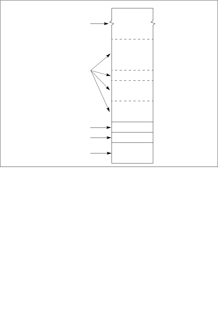
10-26 Vol. 3A
MEMORY CACHE CONTROL
10.11.1 MTRR Feature Identification
The availability of the MTRR feature is model-specific. Software can determine if MTRRs are
supported on a processor by executing the CPUID instruction and reading the state of the MTRR
flag (bit 12) in the feature information register (EDX).
If the MTRR flag is set (indicating that the processor implements MTRRs), additional informa-
tion about MTRRs can be obtained from the 64-bit IA32_MTRRCAP MSR (named MTRRcap
MSR for the P6 family processors). The IA32_MTRRCAP MSR is a read-only MSR that can
be read with the RDMSR instruction. Figure 10-4 shows the contents of the IA32_MTRRCAP
MSR. The functions of the flags and field in this register are as follows:
•VCNT (variable range registers count) field, bits 0 through 7 — Indicates the number
of variable ranges implemented on the processor. The Pentium 4, Intel Xeon, and P6
family processors have eight pairs of MTRRs for setting up eight variable ranges.
•FIX (fixed range registers supported) flag, bit 8 — Fixed range MTRRs
(IA32_MTRR_FIX64K_00000 through IA32_MTRR_FIX4K_0F8000) are supported
when set; no fixed range registers are supported when clear.
Figure 10-3. Mapping Physical Memory With MTRRs
0
FFFFFFFFH
80000H
BFFFFH
C0000H
FFFFFH
100000H
7FFFFH
512 KBytes
256 KBytes
256 KBytes
8 fixed ranges
16 fixed ranges
64 fixed ranges
8 variable ranges
(64-KBytes each)
(16 KBytes each)
(4 KBytes each)
(from 4 KBytes to
maximum size of
Address ranges not
Physical Memory
mapped by an MTRR
are set to a default type
physical memory)
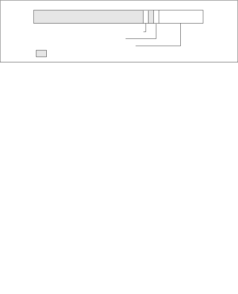
Vol. 3A 10-27
MEMORY CACHE CONTROL
•WC (write combining) flag, bit 10 — The write-combining (WC) memory type is
supported when set; the WC type is not supported when clear.
Bit 9 and bits 11 through 63 in the IA32_MTRRCAP MSR are reserved. If software attempts to
write to the IA32_MTRRCAP MSR, a general-protection exception (#GP) is generated.
For the Pentium 4, Intel Xeon, and P6 family processors, the IA32_MTRRCAP MSR always
contains the value 508H.
10.11.2 Setting Memory Ranges with MTRRs
The memory ranges and the types of memory specified in each range are set by three groups of
registers: the IA32_MTRR_DEF_TYPE MSR, the fixed-range MTRRs, and the variable range
MTRRs. These registers can be read and written to using the RDMSR and WRMSR instruc-
tions, respectively. The IA32_MTRRCAP MSR indicates the availability of these registers on
the processor (see Section 10.11.1, “MTRR Feature Identification”).
10.11.2.1 IA32_MTRR_DEF_TYPE MSR
The IA32_MTRR_DEF_TYPE MSR (named MTRRdefType MSR for the P6 family proces-
sors) sets the default properties of the regions of physical memory that are not encompassed by
MTRRs. The functions of the flags and field in this register are as follows:
•Type field, bits 0 through 7 — Indicates the default memory type used for those physical
memory address ranges that do not have a memory type specified for them by an MTRR
(see Table 10-8 for the encoding of this field). The legal values for this field are 0, 1, 4, 5,
and 6. All other values result in a general-protection exception (#GP) being generated.
Intel recommends the use of the UC (uncached) memory type for all physical memory
addresses where memory does not exist. To assign the UC type to nonexistent memory
locations, it can either be specified as the default type in the Type field or be explicitly
assigned with the fixed and variable MTRRs.
Figure 10-4. IA32_MTRRCAP Register
VCNT — Number of variable range registers
FIX — Fixed range registers supported
WC — Write-combining memory type supported
63 0
Reserved W
C
71011
VCNT
F
I
X
89
Reserved

10-28 Vol. 3A
MEMORY CACHE CONTROL
•FE (fixed MTRRs enabled) flag, bit 10 — Fixed-range MTRRs are enabled when set;
fixed-range MTRRs are disabled when clear. When the fixed-range MTRRs are enabled,
they take priority over the variable-range MTRRs when overlaps in ranges occur. If the
fixed-range MTRRs are disabled, the variable-range MTRRs can still be used and can map
the range ordinarily covered by the fixed-range MTRRs.
•E (MTRRs enabled) flag, bit 11 — MTRRs are enabled when set; all MTRRs are
disabled when clear, and the UC memory type is applied to all of physical memory. When
this flag is set, the FE flag can disable the fixed-range MTRRs; when the flag is clear, the
FE flag has no affect. When the E flag is set, the type specified in the default memory type
field is used for areas of memory not already mapped by either a fixed or variable MTRR.
Bits 8 and 9, and bits 12 through 63, in the IA32_MTRR_DEF_TYPE MSR are reserved; the
processor generates a general-protection exception (#GP) if software attempts to write nonzero
values to them.
10.11.2.2 Fixed Range MTRRs
The fixed memory ranges are mapped with 11 fixed-range registers of 64 bits each. Each of these
registers is divided into 8-bit fields that are used to specify the memory type for each of the sub-
ranges the register controls:
•Register IA32_MTRR_FIX64K_00000 — Maps the 512-KByte address range from 0H
to 7FFFFH. This range is divided into eight 64-KByte sub-ranges.
•Registers IA32_MTRR_FIX16K_80000 and IA32_MTRR_FIX16K_A0000 — Maps
the two 128-KByte address ranges from 80000H to BFFFFH. This range is divided into
sixteen 16-KByte sub-ranges, 8 ranges per register.
•Registers IA32_MTRR_FIX4K_C0000 through IA32_MTRR_FIX4K_F8000 —
Maps eight 32-KByte address ranges from C0000H to FFFFFH. This range is divided into
sixty-four 4-KByte sub-ranges, 8 ranges per register.
Table 10-9 shows the relationship between the fixed physical-address ranges and the corre-
sponding fields of the fixed-range MTRRs; Table 10-8 shows memory type encoding for
MTRRs.
Figure 10-5. IA32_MTRR_DEF_TYPE MSR
Type — Default memory type
FE — Fixed-range MTRRs enable/disable
E — MTRR enable/disable
63 0
Reserved F
E
71011
Type
8912
E
Reserved

Vol. 3A 10-29
MEMORY CACHE CONTROL
For the P6 family processors, the prefix for the fixed range MTRRs is MTRRfix.
10.11.2.3 Variable Range MTRRs
The Pentium 4, Intel Xeon, and P6 family processors permit software to specify the memory
type for eight variable-size address ranges, using a pair of MTRRs for each range. The first entry
in each pair (IA32_MTRR_PHYSBASEn) defines the base address and memory type for the
range; the second entry (IA32_MTRR_PHYSMASKn) contains a mask used to determine the
address range. The “n” suffix indicates register pairs 0 through 7.
For P6 family processors, the prefixes for these variable range MTRRs are MTRRphysBase and
MTRRphysMask.
Figure 10-6 shows flags and fields in these registers. The functions of these flags and fields are:
•Type field, bits 0 through 7 — Specifies the memory type for the range (see Table 10-8
for the encoding of this field).
Table 10-9. Address Mapping for Fixed-Range MTRRs
Address Range (hexadecimal) MTRR
63 56 55 48 47 40 39 32 31 24 23 16 15 8 7 0
70000-
7FFFF 60000-
6FFFF 50000-
5FFFF 40000-
4FFFF 30000-
3FFFF 20000-
2FFFF 10000-
1FFFF 00000-
0FFFF IA32_MTRR_
FIX64K_00000
9C000
9FFFF 98000-
98FFF 94000-
97FFF 90000-
93FFF 8C000-
8FFFF 88000-
8BFFF 84000-
87FFF 80000-
83FFF IA32_MTRR_
FIX16K_80000
BC000
BFFFF B8000-
BBFFF B4000-
B7FFF B0000-
B3FFF AC000-
AFFFF A8000-
ABFFF A4000-
A7FFF A0000-
A3FFF IA32_MTRR_
FIX16K_A0000
C7000
C7FFF C6000-
C6FFF C5000-
C5FFF C4000-
C4FFF C3000-
C3FFF C2000-
C2FFF C1000-
C1FFF C0000-
C0FFF IA32_MTRR_
FIX4K_C0000
CF000
CFFFF CE000-
CEFFF CD000-
CDFFF CC000-
CCFFF CB000-
CBFFF CA000-
CAFFF C9000-
C9FFF C8000-
C8FFF IA32_MTRR_
FIX4K_C8000
D7000
D7FFF D6000-
D6FFF D5000-
D5FFF D4000-
D4FFF D3000-
D3FFF D2000-
D2FFF D1000-
D1FFF D0000-
D0FFF IA32_MTRR_
FIX4K_D0000
DF000
DFFFF DE000-
DEFFF DD000-
DDFFF DC000-
DCFFF DB000-
DBFFF DA000-
DAFFF D9000-
D9FFF D8000-
D8FFF IA32_MTRR_
FIX4K_D8000
E7000
E7FFF E6000-
E6FFF E5000-
E5FFF E4000-
E4FFF E3000-
E3FFF E2000-
E2FFF E1000-
E1FFF E0000-
E0FFF IA32_MTRR_
FIX4K_E0000
EF000
EFFFF EE000-
EEFFF ED000-
EDFFF EC000-
ECFFF EB000-
EBFFF EA000-
EAFFF E9000-
E9FFF E8000-
E8FFF IA32_MTRR_
FIX4K_E8000
F7000
F7FFF F6000-
F6FFF F5000-
F5FFF F4000-
F4FFF F3000-
F3FFF F2000-
F2FFF F1000-
F1FFF F0000-
F0FFF IA32_MTRR_
FIX4K_F0000
FF000
FFFFF FE000-
FEFFF FD000-
FDFFF FC000-
FCFFF FB000-
FBFFF FA000-
FAFFF F9000-
F9FFF F8000-
F8FFF IA32_MTRR_
FIX4K_F8000

10-30 Vol. 3A
MEMORY CACHE CONTROL
•PhysBase field, bits 12 through (MAXPHYADDR-1) — Specifies the base address of
the address range. This 24-bit value, in the case where MAXPHYADDR is 36 bits, is
extended by 12 bits at the low end to form the base address (this automatically aligns the
address on a 4-KByte boundary).
•PhysMask field, bits 12 through (MAXPHYADDR-1) — Specifies a mask (24 bits if the
maximum physical address size is 36 bits, 28 bits if the maximum physical address size is
40 bits). The mask determines the range of the region being mapped, according to the
following relationships:
— Address_Within_Range AND PhysMask = PhysBase AND PhysMask
— This value is extended by 12 bits at the low end to form the mask value. For more
information: see Section 10.11.3, “Example Base and Mask Calculations.”
— The width of the PhysMask field depends on the maximum physical address size
supported by the processor.
CPUID.80000008H reports the maximum physical address size supported by the
processor. If CPUID.80000008H is not available, software may assume that the
processor supports a 36-bit physical address size (then PhysMask is 24 bits wide and
the upper 28 bits of IA32_MTRR_PHYSMASKn are reserved). See the Note below.
•V (valid) flag, bit 11 — Enables the register pair when set; disables register pair when
clear.
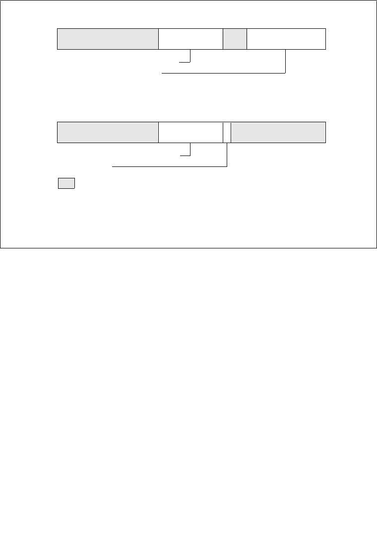
Vol. 3A 10-31
MEMORY CACHE CONTROL
All other bits in the IA32_MTRR_PHYSBASEn and IA32_MTRR_PHYSMASKn registers are
reserved; the processor generates a general-protection exception (#GP) if software attempts to
write to them.
Some mask values can result in ranges that are not continuous. In such ranges, the area not
mapped by the mask value is set to the default memory type. Intel does not encourage the use of
“discontinuous” ranges because they could require physical memory to be present throughout the
entire 4-GByte physical memory map. If memory is not provided, the behaviour is undefined.
NOTE
It is possible for software to parse the memory descriptions that BIOS
provides by using the ACPI/INT15 e820 interface mechanism. This
information then can be used to determine how MTRRs are initialized (for
example: allowing the BIOS to define valid memory ranges and the
maximum memory range supported by the platform, including the processor).
See Section 10.11.4.1, “MTRR Precedences,” for information on overlapping variable MTRR
ranges.
Figure 10-6. IA32_MTRR_PHYSBASEn and IA32_MTRR_PHYSMASKn Variable-Range
Register Pair
V — Valid
PhysMask — Sets range mask
IA32_MTRR_PHYSMASKn Register
63 0
Reserved
101112
VReserved
MAXPHYADDR
PhysMask
Type — Memory type for range
PhysBase — Base address of range
IA32_MTRR_PHYSBASEn Register
63 0
Reserved
1112
Type
MAXPHYADDR
PhysBase
78
Reserved
MAXPHYADDR: The bit position indicated by MAXPHYADDR depends on the maximum
physical address range supported by the processor. It is reported by CPUID leaf
function 80000008H. If CPUID does not support leaf 80000008H, the processor
supports 36-bit physical address size, then bit PhysMask consists of bits 35:12, and
bits 63:36 are reserved.

10-32 Vol. 3A
MEMORY CACHE CONTROL
10.11.3 Example Base and Mask Calculations
The examples in this section apply to processors that support a maximum physical address size
of 36 bits. The base and mask values entered in variable-range MTRR pairs are 24-bit values
that the processor extends to 36-bits.
For example, to enter a base address of 2 MBytes (200000H) in the IA32_MTRR_PHYSBASE3
register, the 12 least-significant bits are truncated and the value 000200H is entered in the Phys-
Base field. The same operation must be performed on mask values. For example, to map the
address range from 200000H to 3FFFFFH (2 MBytes to 4 MBytes), a mask value of
FFFE00000H is required. Again, the 12 least-significant bits of this mask value are truncated,
so that the value entered in the PhysMask field of IA32_MTRR_PHYSMASK3 is FFFE00H.
This mask is chosen so that when any address in the 200000H to 3FFFFFH range is AND’d with
the mask value, it will return the same value as when the base address is AND’d with the mask
value (which is 200000H).
To map the address range from 400000H to 7FFFFFH (4 MBytes to 8 MBytes), a base value of
000400H is entered in the PhysBase field and a mask value of FFFC00H is entered in the Phys-
Mask field.
Example 10-14. Setting-Up Memory for a System
Here is an example of setting up the MTRRs for an system. Assume that the system has the
following characteristics:
•96 MBytes of system memory is mapped as write-back memory (WB) for highest system
performance.
•A custom 4-MByte I/O card is mapped to uncached memory (UC) at a base address of
64 MBytes. This restriction forces the 96 MBytes of system memory to be addressed from
0 to 64 MBytes and from 68 MBytes to 100 MBytes, leaving a 4-MByte hole for the I/O
card.
•An 8-MByte graphics card is mapped to write-combining memory (WC) beginning at
address A0000000H.
•The BIOS area from 15 MBytes to 16 MBytes is mapped to UC memory.

Vol. 3A 10-33
MEMORY CACHE CONTROL
The following settings for the MTRRs will yield the proper mapping of the physical address
space for this system configuration.
IA32_MTRR_PHYSBASE0 = 0000 0000 0000 0006H
IA32_MTRR_PHYSMASK0 = 0000 000F FC00 0800H
Caches 0-64 MByte as WB cache type.
IA32_MTRR_PHYSBASE1 = 0000 0000 0400 0006H
IA32_MTRR_PHYSMASK1 = 0000 000F FE00 0800H
Caches 64-96 MByte as WB cache type.
IA32_MTRR_PHYSBASE2 = 0000 0000 0600 0006H
IA32_MTRR_PHYSMASK2 = 0000 000F FFC0 0800H
Caches 96-100 MByte as WB cache type.
IA32_MTRR_PHYSBASE3 = 0000 0000 0400 0000H
IA32_MTRR_PHYSMASK3 = 0000 000F FFC0 0800H
Caches 64-68 MByte as UC cache type.
IA32_MTRR_PHYSBASE4 = 0000 0000 00F0 0000H
IA32_MTRR_PHYSMASK4 = 0000 000F FFF0 0800H
Caches 15-16 MByte as UC cache type.
IA32_MTRR_PHYSBASE5 = 0000 0000 A000 0001H
IA32_MTRR_PHYSMASK5 = 0000 000F FF80 0800H
Caches A0000000-A0800000 as WC type.
This MTRR setup uses the ability to overlap any two memory ranges (as long as the ranges are
mapped to WB and UC memory types) to minimize the number of MTRR registers that are
required to configure the memory environment. This setup also fulfills the requirement that two
register pairs are left for operating system usage.
10.11.3.1 Base and Mask Calculations with Intel EM64T
For IA-32 processors that support greater than 36 bits of physical address size, software should
query CPUID.80000008H to determine the maximum physical address.
Example 10-15. Setting-Up Memory for a System with a 40-Bit Address Size
If a processor supports 40-bits of physical address size, then the PhysMask field (in
IA32_MTRR_PHYSMASKn registers) is 28 bits instead of 24 bits. For this situation, Example
10-14 should be modified as follows:
IA32_MTRR_PHYSBASE0 = 0000 0000 0000 0006H
IA32_MTRR_PHYSMASK0 = 0000 00FF FC00 0800H
Caches 0-64 MByte as WB cache type.
IA32_MTRR_PHYSBASE1 = 0000 0000 0400 0006H
IA32_MTRR_PHYSMASK1 = 0000 00FF FE00 0800H
Caches 64-96 MByte as WB cache type.
IA32_MTRR_PHYSBASE2 = 0000 0000 0600 0006H
IA32_MTRR_PHYSMASK2 = 0000 00FF FFC0 0800H

10-34 Vol. 3A
MEMORY CACHE CONTROL
Caches 96-100 MByte as WB cache type.
IA32_MTRR_PHYSBASE3 = 0000 0000 0400 0000H
IA32_MTRR_PHYSMASK3 = 0000 00FF FFC0 0800H
Caches 64-68 MByte as UC cache type.
IA32_MTRR_PHYSBASE4 = 0000 0000 00F0 0000H
IA32_MTRR_PHYSMASK4 = 0000 00FF FFF0 0800H
Caches 15-16 MByte as UC cache type.
IA32_MTRR_PHYSBASE5 = 0000 0000 A000 0001H
IA32_MTRR_PHYSMASK5 = 0000 00FF FF80 0800H
Caches A0000000-A0800000 as WC type.
10.11.4 Range Size and Alignment Requirement
The range that is to be mapped to a variable-range MTRR must meet the following “power of
2” size and alignment rules:
1. The minimum range size is 4 KBytes, and the base address of this range must be on at least
a 4-KByte boundary.
2. For ranges greater than 4 KBytes, each range must be of length 2n and its base address
must be aligned on a 2n boundary, where n is a value equal to or greater than 12. The base-
address alignment value cannot be less than its length. For example, an 8-KByte range
cannot be aligned on a 4-KByte boundary. It must be aligned on at least an 8-KByte
boundary.
10.11.4.1 MTRR Precedences
If the MTRRs are not enabled (by setting the E flag in the IA32_MTRR_DEF_TYPE MSR),
then all memory accesses are of the UC memory type. If the MTRRs are enabled, then the
memory type used for a memory access is determined as follows:
1. If the physical address falls within the first 1 MByte of physical memory and fixed MTRRs
are enabled, the processor uses the memory type stored for the appropriate fixed-range
MTRR.
2. Otherwise, the processor attempts to match the physical address with a memory type set by
the variable-range MTRRs:
a. If one variable memory range matches, the processor uses the memory type stored in
the IA32_MTRR_PHYSBASEn register for that range.
b. If two or more variable memory ranges match and the memory types are identical,
then that memory type is used.
c. If two or more variable memory ranges match and one of the memory types is UC, the
UC memory type used.

Vol. 3A 10-35
MEMORY CACHE CONTROL
d. If two or more variable memory ranges match and the memory types are WT and WB,
the WT memory type is used.
e. For overlaps not defined by the above rules, processor behavior is undefined.
3. If no fixed or variable memory range matches, the processor uses the default memory type.
10.11.5 MTRR Initialization
On a hardware reset, a Pentium 4, Intel Xeon, or P6 family processor clears the valid flags in the
variable-range MTRRs and clears the E flag in the IA32_MTRR_DEF_TYPE MSR to disable
all MTRRs. All other bits in the MTRRs are undefined. Prior to initializing the MTRRs, soft-
ware (normally the system BIOS) must initialize all fixed-range and variable-range MTRR
registers fields to 0. Software can then initialize the MTRRs according to the types of memory
known to it, including memory on devices that it auto-configures. This initialization is expected
to occur prior to booting the operating system.
See Section 10.11.8, “MTRR Considerations in MP Systems,” for information on initializing
MTRRs in MP (multiple-processor) systems.
10.11.6 Remapping Memory Types
A system designer may re-map memory types to tune performance or because a future processor
may not implement all memory types supported by the Pentium 4, Intel Xeon, and P6 family
processors. The following rules support coherent memory-type re-mappings:
1. A memory type should not be mapped into another memory type that has a weaker
memory ordering model. For example, the uncacheable type cannot be mapped into any
other type, and the write-back, write-through, and write-protected types cannot be mapped
into the weakly ordered write-combining type.
2. A memory type that does not delay writes should not be mapped into a memory type that
does delay writes, because applications of such a memory type may rely on its write-
through behavior. Accordingly, the write-back type cannot be mapped into the write-
through type.
3. A memory type that views write data as not necessarily stored and read back by a
subsequent read, such as the write-protected type, can only be mapped to another type with
the same behaviour (and there are no others for the Pentium 4, Intel Xeon, and P6 family
processors) or to the uncacheable type.
In many specific cases, a system designer can have additional information about how a memory
type is used, allowing additional mappings. For example, write-through memory with no asso-
ciated write side effects can be mapped into write-back memory.

10-36 Vol. 3A
MEMORY CACHE CONTROL
10.11.7 MTRR Maintenance Programming Interface
The operating system maintains the MTRRs after booting and sets up or changes the memory
types for memory-mapped devices. The operating system should provide a driver and applica-
tion programming interface (API) to access and set the MTRRs. The function calls
MemTypeGet() and MemTypeSet() define this interface.
10.11.7.1 MemTypeGet() Function
The MemTypeGet() function returns the memory type of the physical memory range specified
by the parameters base and size. The base address is the starting physical address and the size is
the number of bytes for the memory range. The function automatically aligns the base address
and size to 4-KByte boundaries. Pseudocode for the MemTypeGet() function is given in
Example 10-16.
Example 10-16. MemTypeGet() Pseudocode
#define MIXED_TYPES -1 /* 0 < MIXED_TYPES || MIXED_TYPES > 256 */
IF CPU_FEATURES.MTRR /* processor supports MTRRs */
THEN
Align BASE and SIZE to 4-KByte boundary;
IF (BASE + SIZE) wrap 4-GByte address space
THEN return INVALID;
FI;
IF MTRRdefType.E = 0
THEN return UC;
FI;
FirstType ← Get4KMemType (BASE);
/* Obtains memory type for first 4-KByte range. */
/* See Get4KMemType (4KByteRange) in Example 10-17. */
FOR each additional 4-KByte range specified in SIZE
NextType ← Get4KMemType (4KByteRange);
IF NextType ≠ FirstType
THEN return MixedTypes;
FI;
ROF;
return FirstType;
ELSE return UNSUPPORTED;
FI;
If the processor does not support MTRRs, the function returns UNSUPPORTED. If the MTRRs
are not enabled, then the UC memory type is returned. If more than one memory type corre-
sponds to the specified range, a status of MIXED_TYPES is returned. Otherwise, the memory
type defined for the range (UC, WC, WT, WB, or WP) is returned.

Vol. 3A 10-37
MEMORY CACHE CONTROL
The pseudocode for the Get4KMemType() function in Example 10-17 obtains the memory type
for a single 4-KByte range at a given physical address. The sample code determines whether an
PHY_ADDRESS falls within a fixed range by comparing the address with the known fixed
ranges: 0 to 7FFFFH (64-KByte regions), 80000H to BFFFFH (16-KByte regions), and C0000H
to FFFFFH (4-KByte regions). If an address falls within one of these ranges, the appropriate bits
within one of its MTRRs determine the memory type.
Example 10-17. Get4KMemType() Pseudocode
IF IA32_MTRRCAP.FIX AND MTRRdefType.FE /* fixed registers enabled */
THEN IF PHY_ADDRESS is within a fixed range
return IA32_MTRR_FIX.Type;
FI;
FOR each variable-range MTRR in IA32_MTRRCAP.VCNT
IF IA32_MTRR_PHYSMASK.V = 0
THEN continue;
FI;
IF (PHY_ADDRESS AND IA32_MTRR_PHYSMASK.Mask) =
(IA32_MTRR_PHYSBASE.Base
AND IA32_MTRR_PHYSMASK.Mask)
THEN
return IA32_MTRR_PHYSBASE.Type;
FI;
ROF;
return MTRRdefType.Type;
10.11.7.2 MemTypeSet() Function
The MemTypeSet() function in Example 10-18 sets a MTRR for the physical memory range
specified by the parameters base and size to the type specified by type. The base address and
size are multiples of 4 KBytes and the size is not 0.
Example 10-18. MemTypeSet Pseudocode
IF CPU_FEATURES.MTRR (* processor supports MTRRs *)
THEN
IF BASE and SIZE are not 4-KByte aligned or size is 0
THEN return INVALID;
FI;
IF (BASE + SIZE) wrap 4-GByte address space
THEN return INVALID;
FI;
IF TYPE is invalid for Pentium 4, Intel Xeon, and P6 family processors
THEN return UNSUPPORTED;
FI;
IF TYPE is WC and not supported
THEN return UNSUPPORTED;

10-38 Vol. 3A
MEMORY CACHE CONTROL
FI;
IF IA32_MTRRCAP.FIX is set AND range can be mapped using a fixed-range MTRR
THEN
pre_mtrr_change();
update affected MTRR;
post_mtrr_change();
FI;
ELSE (* try to map using a variable MTRR pair *)
IF IA32_MTRRCAP.VCNT = 0
THEN return UNSUPPORTED;
FI;
IF conflicts with current variable ranges
THEN return RANGE_OVERLAP;
FI;
IF no MTRRs available
THEN return VAR_NOT_AVAILABLE;
FI;
IF BASE and SIZE do not meet the power of 2 requirements for variable MTRRs
THEN return INVALID_VAR_REQUEST;
FI;
pre_mtrr_change();
Update affected MTRRs;
post_mtrr_change();
FI;
pre_mtrr_change()
BEGIN
disable interrupts;
Save current value of CR4;
disable and flush caches;
flush TLBs;
disable MTRRs;
IF multiprocessing
THEN maintain consistency through IPIs;
FI;
END
post_mtrr_change()
BEGIN
flush caches and TLBs;
enable MTRRs;
enable caches;
restore value of CR4;
enable interrupts;
END

Vol. 3A 10-39
MEMORY CACHE CONTROL
The physical address to variable range mapping algorithm in the MemTypeSet function detects
conflicts with current variable range registers by cycling through them and determining whether
the physical address in question matches any of the current ranges. During this scan, the algo-
rithm can detect whether any current variable ranges overlap and can be concatenated into a
single range.
The pre_mtrr_change() function disables interrupts prior to changing the MTRRs, to avoid
executing code with a partially valid MTRR setup. The algorithm disables caching by setting
the CD flag and clearing the NW flag in control register CR0. The caches are invalidated using
the WBINVD instruction. The algorithm flushes all TLB entries either by clearing the page-
global enable (PGE) flag in control register CR4 (if PGE was already set) or by updating control
register CR3 (if PGE was already clear). Finally, it disables MTRRs by clearing the E flag in the
IA32_MTRR_DEF_TYPE MSR.
After the memory type is updated, the post_mtrr_change() function re-enables the MTRRs and
again invalidates the caches and TLBs. This second invalidation is required because of the
processor's aggressive prefetch of both instructions and data. The algorithm restores interrupts
and re-enables caching by setting the CD flag.
An operating system can batch multiple MTRR updates so that only a single pair of cache inval-
idations occur.
10.11.8 MTRR Considerations in MP Systems
In MP (multiple-processor) systems, the operating systems must maintain MTRR consistency
between all the processors in the system. The Pentium 4, Intel Xeon, and P6 family processors
provide no hardware support to maintain this consistency. In general, all processors must have
the same MTRR values.
This requirement implies that when the operating system initializes an MP system, it must load
the MTRRs of the boot processor while the E flag in register MTRRdefType is 0. The operating
system then directs other processors to load their MTRRs with the same memory map. After all
the processors have loaded their MTRRs, the operating system signals them to enable their
MTRRs. Barrier synchronization is used to prevent further memory accesses until all processors
indicate that the MTRRs are enabled. This synchronization is likely to be a shoot-down style
algorithm, with shared variables and interprocessor interrupts.
Any change to the value of the MTRRs in an MP system requires the operating system to repeat
the loading and enabling process to maintain consistency, using the following procedure:
1. Broadcast to all processors to execute the following code sequence.
2. Disable interrupts.
3. Wait for all processors to reach this point.
4. Enter the no-fill cache mode. (Set the CD flag in control register CR0 to 1 and the NW flag
to 0.)
5. Flush all caches using the WBINVD instructions. Note on a processor that supports self-
snooping, CPUID feature flag bit 27, this step is unnecessary.

10-40 Vol. 3A
MEMORY CACHE CONTROL
6. If the PGE flag is set in control register CR4, flush all TLBs by clearing that flag.
7. If the PGE flag is clear in control register CR4, flush all TLBs by executing a MOV from
control register CR3 to another register and then a MOV from that register back to CR3.
8. Disable all range registers (by clearing the E flag in register MTRRdefType). If only
variable ranges are being modified, software may clear the valid bits for the affected
register pairs instead.
9. Update the MTRRs.
10. Enable all range registers (by setting the E flag in register MTRRdefType). If only
variable-range registers were modified and their individual valid bits were cleared, then set
the valid bits for the affected ranges instead.
11. Flush all caches and all TLBs a second time. (The TLB flush is required for Pentium 4,
Intel Xeon, and P6 family processors. Executing the WBINVD instruction is not needed
when using Pentium 4, Intel Xeon, and P6 family processors, but it may be needed in
future systems.)
12. Enter the normal cache mode to re-enable caching. (Set the CD and NW flags in control
register CR0 to 0.)
13. Set PGE flag in control register CR4, if cleared in Step 6 (above).
14. Wait for all processors to reach this point.
15. Enable interrupts.
10.11.9 Large Page Size Considerations
The MTRRs provide memory typing for a limited number of regions that have a 4 KByte gran-
ularity (the same granularity as 4-KByte pages). The memory type for a given page is cached in
the processor’s TLBs. When using large pages (2 or 4 MBytes), a single page-table entry covers
multiple 4-KByte granules, each with a single memory type. Because the memory type for a
large page is cached in the TLB, the processor can behave in an undefined manner if a large page
is mapped to a region of memory that MTRRs have mapped with multiple memory types.
Undefined behavior can be avoided by insuring that all MTRR memory-type ranges within a
large page are of the same type. If a large page maps to a region of memory containing different
MTRR-defined memory types, the PCD and PWT flags in the page-table entry should be set for
the most conservative memory type for that range. For example, a large page used for memory
mapped I/O and regular memory is mapped as UC memory. Alternatively, the operating system
can map the region using multiple 4-KByte pages each with its own memory type.
The requirement that all 4-KByte ranges in a large page are of the same memory type implies
that large pages with different memory types may suffer a performance penalty, since they must
be marked with the lowest common denominator memory type.

Vol. 3A 10-41
MEMORY CACHE CONTROL
The Pentium 4, Intel Xeon, and P6 family processors provide special support for the physical
memory range from 0 to 4 MBytes, which is potentially mapped by both the fixed and vari-
able MTRRs. This support is invoked when a Pentium 4, Intel Xeon, or P6 family processor
detects a large page overlapping the first 1 MByte of this memory range with a memory type
that conflicts with the fixed MTRRs. Here, the processor maps the memory range as multiple
4-KByte pages within the TLB. This operation insures correct behavior at the cost of perfor-
mance. To avoid this performance penalty, operating-system software should reserve the
large page option for regions of memory at addresses greater than or equal to 4 MBytes.
10.12 PAGE ATTRIBUTE TABLE (PAT)
The Page Attribute Table (PAT) extends the IA-32 architecture’s page-table format to allow
memory types to be assigned to regions of physical memory based on linear address mappings.
The PAT is a companion feature to the MTRRs; that is, the MTRRs allow mapping of memory
types to regions of the physical address space, where the PAT allows mapping of memory types
to pages within the linear address space. The MTRRs are useful for statically describing memory
types for physical ranges, and are typically set up by the system BIOS. The PAT extends the
functions of the PCD and PWT bits in page tables to allow all five of the memory types that can
be assigned with the MTRRs (plus one additional memory type) to also be assigned dynamically
to pages of the linear address space.
The PAT was introduced into the IA-32 architecture in the Pentium III processor and is also
available in the Pentium 4 and Intel Xeon processors.
NOTE
In multiple processor systems, the operating system must maintain MTRR
consistency between all the processors in the system (that is, all processors
must use the same MTRR values). The Pentium 4, Intel Xeon, and P6 family
processors provide no hardware support for maintaining this consistency.
10.12.1 Detecting Support for the PAT Feature
An operating system or executive can detect the availability of the PAT by executing the CPUID
instruction with a value of 1 in the EAX register. Support for the PAT is indicated by the PAT
flag (bit 16 of the values returned to EDX register). If the PAT is supported, the operating system
or executive can use the IA32_CR_PAT MSR to program the PAT. When memory types have
been assigned to entries in the PAT, software can then use of the PAT-index bit (PAT) in the page-
table and page-directory entries along with the PCD and PWT bits to assign memory types from
the PAT to individual pages.
Note that there is no separate flag or control bit in any of the control registers that enables the
PAT. The PAT is always enabled on all processors that support it, and the table lookup always
occurs whenever paging is enabled, in all paging modes.

10-42 Vol. 3A
MEMORY CACHE CONTROL
10.12.2 IA32_CR_PAT MSR
The IA32_CR_PAT MSR is located at MSR address 277H (see to Appendix B, “Model-Specific
Registers (MSRs),” and this address will remain at the same address on future IA-32 processors
that support the PAT feature. Figure 10-7 shows the format of the 64-bit IA32_CR_PAT MSR.
The IA32_CR_PAT MSR contains eight page attribute fields: PA0 through PA7. The three low-
order bits of each field are used to specify a memory type. The five high-order bits of each field
are reserved, and must be set to all 0s. Each of the eight page attribute fields can contain any of
the memory type encodings specified in Table 10-10.
Figure 10-7. IA32_CR_PAT MSR
Note that for the P6 family processors, the IA32_CR_PAT MSR is named the PAT MSR.
31 27 26 24 23 19 18 16 15 11 10 8 7 3 2 0
Reserved PA3 Reserved PA2 Reserved PA1 Reserved PA0
63 59 58 56 55 51 50 48 47 43 42 40 39 35 34 32
Reserved PA7 Reserved PA6 Reserved PA5 Reserved PA4
Table 10-10. Memory Types That Can Be Encoded With PAT
Encoding Mnemonic
00H Uncacheable (UC)
01H Write Combining (WC)
02H Reserved*
03H Reserved*
04H Write Through (WT)
05H Write Protected (WP)
06H Write Back (WB)
07H Uncached (UC-)
08H - FFH Reserved*
NOTE:
* Using these encodings will result in a general-protection exception (#GP).

Vol. 3A 10-43
MEMORY CACHE CONTROL
10.12.3 Selecting a Memory Type from the PAT
To select a memory type for a page from the PAT, a 3-bit index made up of the PAT, PCD, and
PWT bits must be encoded in the page-table or page-directory entry for the page. Table 10-11
shows the possible encodings of the PAT, PCD, and PWT bits and the PAT entry selected with
each encoding. The PAT bit is bit 7 in page-table entries that point to 4-KByte pages (see Figures
3-14 and 3-20) and bit 12 in page-directory entries that point to 2-MByte or 4-MByte pages (see
Figures 3-15, 3-21, and 3-23). The PCD and PWT bits are always bits 4 and 3, respectively, in
page-table and page-directory entries.
The PAT entry selected for a page is used in conjunction with the MTRR setting for the region
of physical memory in which the page is mapped to determine the effective memory type for the
page, as shown in Table 10-7.
10.12.4 Programming the PAT
Table 10-12 shows the default setting for each PAT entry following a power up or reset of the
processor. The setting remain unchanged following a soft reset (INIT reset).
Table 10-11. Selection of PAT Entries with PAT, PCD, and PWT Flags
PAT PCD PWT PAT Entry
0 0 0 PAT0
0 0 1 PAT1
0 1 0 PAT2
0 1 1 PAT3
1 0 0 PAT4
1 0 1 PAT5
1 1 0 PAT6
1 1 1 PAT7
Table 10-12. Memory Type Setting of PAT Entries Following a Power-up or Reset
PAT Entry Memory Type Following Power-up or Reset
PAT0 WB
PAT1 WT
PAT2 UC-
PAT3 UC
PAT4 WB
PAT5 WT
PAT6 UC-
PAT7 UC

10-44 Vol. 3A
MEMORY CACHE CONTROL
The values in all the entries of the PAT can be changed by writing to the IA32_CR_PAT MSR
using the WRMSR instruction. The IA32_CR_PAT MSR is read and write accessible (use of
the RDMSR and WRMSR instructions, respectively) to software operating at a CPL of 0.
Table 10-10 shows the allowable encoding of the entries in the PAT. Attempting to write an
undefined memory type encoding into the PAT causes a general-protection (#GP) exception
to be generated.
NOTE
In a multiple processor system, the PATs of all processors must contain the
same values.
The operating system is responsible for insuring that changes to a PAT entry occur in a manner
that maintains the consistency of the processor caches and translation lookaside buffers (TLB).
This is accomplished by following the procedure as specified in Section 10.11.8, “MTRR
Considerations in MP Systems,” for changing the value of an MTRR in a multiple processor
system. It requires a specific sequence of operations that includes flushing the processors caches
and TLBs.
The PAT allows any memory type to be specified in the page tables, and therefore it is possible
to have a single physical page mapped to two or more different linear addresses, each with
different memory types. Intel does not support this practice because it may lead to undefined
operations that can result in a system failure. In particular, a WC page must never be aliased to
a cacheable page because WC writes may not check the processor caches. When remapping a
page that was previously mapped as a cacheable memory type to a WC page, an operating
system can avoid this type of aliasing by doing the following:
1. Remove the previous mapping to a cacheable memory type in the page tables; that is, make
them not present.
2. Flush the TLBs of processors that may have used the mapping, even speculatively.
3. Create a new mapping to the same physical address with a new memory type, for instance,
WC.
4. Flush the caches on all processors that may have used the mapping previously. Note on
processors that support self-snooping, CPUID feature flag bit 27, this step is unnecessary.
Operating systems that use a page directory as a page table (to map large pages) and enable page
size extensions must carefully scrutinize the use of the PAT index bit for the 4-KByte page-table
entries. The PAT index bit for a page-table entry (bit 7) corresponds to the page size bit in a page-
directory entry. Therefore, the operating system can only use PAT entries PA0 through PA3
when setting the caching type for a page table that is also used as a page directory. If the oper-
ating system attempts to use PAT entries PA4 through PA7 when using this memory as a page
table, it effectively sets the PS bit for the access to this memory as a page directory.
For compatibility with earlier IA-32 processors that do not support the PAT, care should be taken
in selecting the encodings for entries in the PAT (see Section 10.12.5, “PAT Compatibility with
Earlier IA-32 Processors”).

Vol. 3A 10-45
MEMORY CACHE CONTROL
10.12.5 PAT Compatibility with Earlier IA-32 Processors
For IA-32 processors that support the PAT, the IA32_CR_PAT MSR is always active. That is,
the PCD and PWT bits in page-table entries and in page-directory entries (that point to pages)
are always select a memory type for a page indirectly by selecting an entry in the PAT. They
never select the memory type for a page directly as they do in earlier IA-32 processors that do
not implement the PAT (see Table 10-6).
To allow compatibility for code written to run on earlier IA-32 processor that do not support the
PAT, the PAT mechanism has been designed to allow backward compatibility to earlier proces-
sors. This compatibility is provided through the ordering of the PAT, PCD, and PWT bits in the
3-bit PAT entry index. For processors that do not implement the PAT, the PAT index bit (bit 7 in
the page-table entries and bit 12 in the page-directory entries) is reserved and set to 0. With the
PAT bit reserved, only the first four entries of the PAT can be selected with the PCD and PWT
bits. At power-up or reset (see Table 10-12), these first four entries are encoded to select the
same memory types as the PCD and PWT bits would normally select directly in an IA-32
processor that does not implement the PAT. So, if encodings of the first four entries in the PAT
are left unchanged following a power-up or reset, code written to run on earlier IA-32 processors
that do not implement the PAT will run correctly on IA-32 processors that do implement the PAT.

10-46 Vol. 3A
MEMORY CACHE CONTROL

11
Intel® MMX™
Technology
System Programming
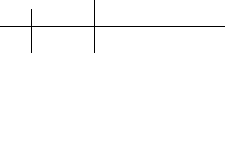
Vol. 3A 11-1
CHAPTER 11
INTEL® MMX™ TECHNOLOGY SYSTEM
PROGRAMMING
This chapter describes those features of the Intel® MMX™ technology that must be considered
when designing or enhancing an operating system to support MMX technology. It covers MMX
instruction set emulation, the MMX state, aliasing of MMX registers, saving MMX state, task
and context switching considerations, exception handling, and debugging.
11.1 EMULATION OF THE MMX INSTRUCTION SET
The IA-32 architecture does not support emulation of the MMX instructions, as it does for x87
FPU instructions. The EM flag in control register CR0 (provided to invoke emulation of x87
FPU instructions) cannot be used for MMX instruction emulation. If an MMX instruction is
executed when the EM flag is set, an invalid opcode exception (UD#) is generated. Table 11-1
shows the interaction of the EM, MP, and TS flags in control register CR0 when executing
MMX instructions.
11.2 THE MMX STATE AND MMX REGISTER ALIASING
The MMX state consists of eight 64-bit registers (MM0 through MM7). These registers are
aliased to the low 64-bits (bits 0 through 63) of floating-point registers R0 through R7 (see
Figure 11-1). Note that the MMX registers are mapped to the physical locations of the floating-
point registers (R0 through R7), not to the relative locations of the registers in the floating-point
register stack (ST0 through ST7). As a result, the MMX register mapping is fixed and is not
affected by value in the Top Of Stack (TOS) field in the floating-point status word (bits 11
through 13).
Table 11-1. Action Taken By MMX Instructions for Different Combinations
of EM, MP and TS
CR0 Flags
EM MP* TS Action
0 1 0 Execute.
0 1 1 #NM exception.
1 1 0 #UD exception.
1 1 1 #UD exception.
NOTE:
* For processors that support the MMX instructions, the MP flag should be set.
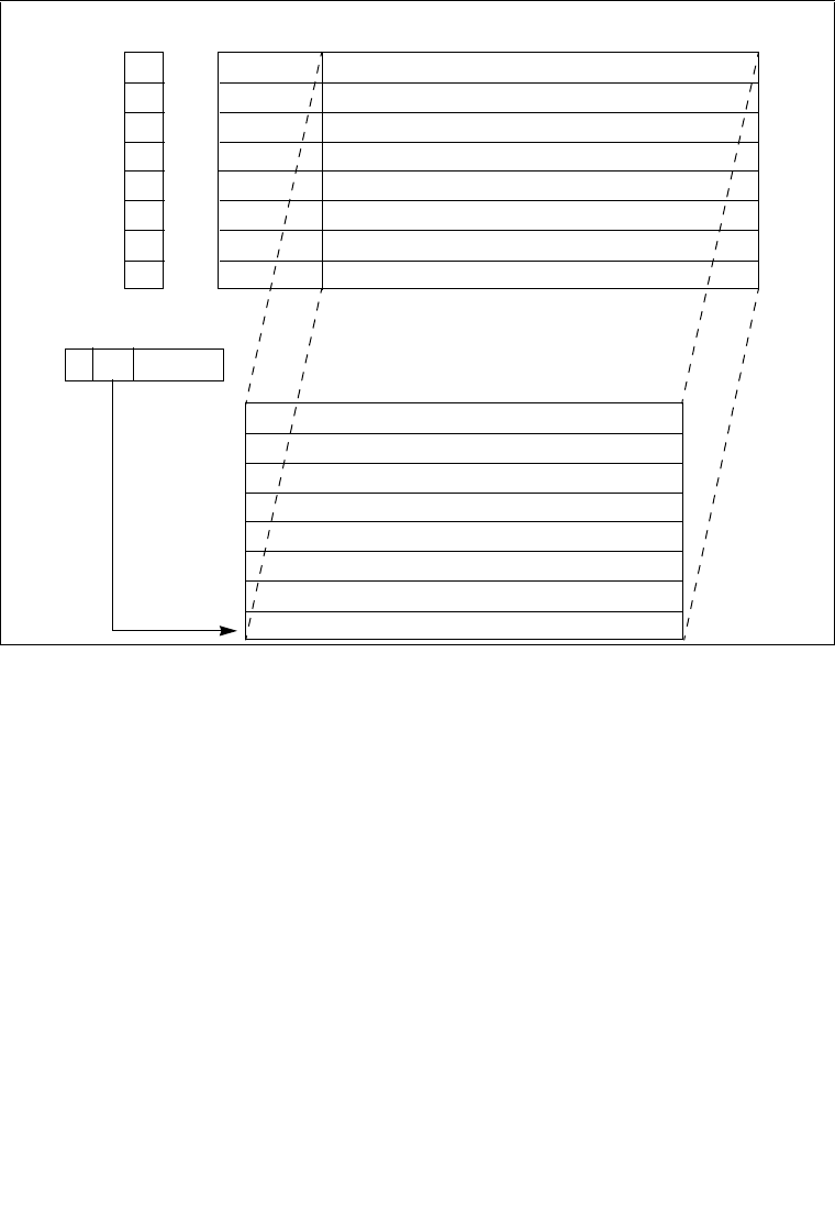
11-2 Vol. 3A
INTEL® MMX™ TECHNOLOGY SYSTEM PROGRAMMING
When a value is written into an MMX register using an MMX instruction, the value also appears
in the corresponding floating-point register in bits 0 through 63. Likewise, when a floating-point
value written into a floating-point register by a x87 FPU, the low 64 bits of that value also
appears in a the corresponding MMX register.
The execution of MMX instructions have several side effects on the x87 FPU state contained in
the floating-point registers, the x87 FPU tag word, and the x87 FPU status word. These side
effects are as follows:
•When an MMX instruction writes a value into an MMX register, at the same time, bits 64
through 79 of the corresponding floating-point register are set to all 1s.
•When an MMX instruction (other than the EMMS instruction) is executed, each of the tag
fields in the x87 FPU tag word is set to 00B (valid). (See also Section 11.2.1, “Effect of
MMX, x87 FPU, FXSAVE, and FXRSTOR Instructions on the x87 FPU Tag Word.”)
•When the EMMS instruction is executed, each tag field in the x87 FPU tag word is set to
11B (empty).
•Each time an MMX instruction is executed, the TOS value is set to 000B.
Figure 11-1. Mapping of MMX Registers to Floating-Point Registers
0
79
R7
R6
R5
R4
R3
R2
R1
R0
Floating-Point Registers
64 63
x87 FPU Status Register
11
13
x87 FPU Tag
MMX Registers
TOS
Register
0
MM7
MM6
MM5
MM4
MM3
MM2
MM1
MM0
63
TOS = 0
00
00
00
00
00
00
00
00
000

Vol. 3A 11-3
INTEL® MMX™ TECHNOLOGY SYSTEM PROGRAMMING
Execution of MMX instructions does not affect the other bits in the x87 FPU status word (bits
0 through 10 and bits 14 and 15) or the contents of the other x87 FPU registers that comprise the
x87 FPU state (the x87 FPU control word, instruction pointer, data pointer, or opcode registers).
Table 11-2 summarizes the effects of the MMX instructions on the x87 FPU state.
11.2.1 Effect of MMX, x87 FPU, FXSAVE, and FXRSTOR
Instructions on the x87 FPU Tag Word
Table 11-3 summarizes the effect of MMX and x87 FPU instructions and the FXSAVE and
FXRSTOR instructions on the tags in the x87 FPU tag word and the corresponding tags in an
image of the tag word stored in memory.
The values in the fields of the x87 FPU tag word do not affect the contents of the MMX registers
or the execution of MMX instructions. However, the MMX instructions do modify the contents
of the x87 FPU tag word, as is described in Section 11.2, “The MMX State and MMX Register
Aliasing.” These modifications may affect the operation of the x87 FPU when executing x87
FPU instructions, if the x87 FPU state is not initialized or restored prior to beginning x87 FPU
instruction execution.
Note that the FSAVE, FXSAVE, and FSTENV instructions (which save x87 FPU state informa-
tion) read the x87 FPU tag register and contents of each of the floating-point registers, determine
the actual tag values for each register (empty, nonzero, zero, or special), and store the updated
tag word in memory. After executing these instructions, all the tags in the x87 FPU tag word are
set to empty (11B). Likewise, the EMMS instruction clears MMX state from the MMX/floating-
point registers by setting all the tags in the x87 FPU tag word to 11B.
Table 11-2. Effects of MMX Instructions on x87 FPU State
MMX
Instruction
Type x87 FPU Tag
Word
TOS Field of
x87 FPU
Status Word Other x87 FPU
Registers
Bits 64 Through
79 of x87 FPU
Data Registers
Bits 0 Through
63 of x87 FPU
Data Registers
Read from
MMX register All tags set to
00B (Valid) 000B Unchanged Unchanged Unchanged
Write to MMX
register All tags set to
00B (Valid) 000B Unchanged Set to all 1s Overwritten with
MMX data
EMMS All fields set to
11B (Empty) 000B Unchanged Unchanged Unchanged

11-4 Vol. 3A
INTEL® MMX™ TECHNOLOGY SYSTEM PROGRAMMING
11.3 SAVING AND RESTORING THE MMX STATE AND
REGISTERS
Because the MMX registers are aliased to the x87 FPU data registers, the MMX state can be
saved to memory and restored from memory as follows:
•Execute an FSAVE, FNSAVE, or FXSAVE instruction to save the MMX state to memory.
(The FXSAVE instruction also saves the state of the XMM and MXCSR registers.)
•Execute an FRSTOR or FXRSTOR instruction to restore the MMX state from memory.
(The FXRSTOR instruction also restores the state of the XMM and MXCSR registers.)
The save and restore methods described above are required for operating systems (see Section
11.4, “Saving MMX State on Task or Context Switches”). Applications can in some cases save
and restore only the MMX registers in the following way:
•Execute eight MOVQ instructions to save the contents of the MMX0 through MMX7
registers to memory. An EMMS instruction may then (optionally) be executed to clear the
MMX state in the x87 FPU.
•Execute eight MOVQ instructions to read the saved contents of MMX registers from
memory into the MMX0 through MMX7 registers.
Table 11-3. Effect of the MMX, x87 FPU, and FXSAVE/FXRSTOR Instructions on the
x87 FPU Tag Word
Instruction
Type Instruction x87 FPU Tag Word Image of x87 FPU Tag Word
Stored in Memory
MMX All (except EMMS) All tags are set to 00B (valid). Not affected.
MMX EMMS All tags are set to 11B (empty). Not affected.
x87 FPU All (except FSAVE,
FSTENV, FRSTOR,
FLDENV)
Tag for modified floating-point
register is set to 00B or 11B. Not affected.
x87 FPU and
FXSAVE FSAVE, FSTENV,
FXSAVE Tags and register values are
read and interpreted; then all
tags are set to 11B.
Tags are set according to the
actual values in the floating-
point registers; that is, empty
registers are marked 11B and
valid registers are marked 00B
(nonzero), 01B (zero), or 10B
(special).
x87 FPU and
FXRSTOR FRSTOR, FLDENV,
FXRSTOR All tags marked 11B in memory
are set to 11B; all other tags are
set according to the value in the
corresponding floating-point
register: 00B (nonzero), 01B
(zero), or 10B (special).
Tags are read and interpreted,
but not modified.

Vol. 3A 11-5
INTEL® MMX™ TECHNOLOGY SYSTEM PROGRAMMING
NOTE
The IA-32 architecture does not support scanning the x87 FPU tag word and
then only saving valid entries.
11.4 SAVING MMX STATE ON TASK OR CONTEXT SWITCHES
When switching from one task or context to another, it is often necessary to save the MMX state.
As a general rule, if the existing task switching code for an operating system includes facilities
for saving the state of the x87 FPU, these facilities can also be relied upon to save the MMX
state, without rewriting the task switch code. This reliance is possible because the MMX state
is aliased to the x87 FPU state (see Section 11.2, “The MMX State and MMX Register
Aliasing”).
With the introduction of the FXSAVE and FXRSTOR instructions and of SSE/SSE2/SSE3
extensions to the IA-32 architecture, it is possible (and more efficient) to create state saving
facilities in the operating system or executive that save the x87 FPU/MMX/SSE/SSE2/SSE3
state in one operation. Section 12.5, “Designing OS Facilities for AUTOMATICALLY Saving
x87 FPU, MMX, and SSE/SSE2/SSE3 state on Task or Context Switches,” describes how to
design such facilities. The techniques describes in this section can be adapted to saving only the
MMX and x87 FPU state if needed.
11.5. EXCEPTIONS THAT CAN OCCUR WHEN EXECUTING MMX
INSTRUCTIONS
MMX instructions do not generate x87 FPU floating-point exceptions, nor do they affect the
processor’s status flags in the EFLAGS register or the x87 FPU status word. The following
exceptions can be generated during the execution of an MMX instruction:
•Exceptions during memory accesses:
— Stack-segment fault (#SS).
— General protection (#GP).
— Page fault (#PF).
— Alignment check (#AC), if alignment checking is enabled.
•System exceptions:
— Invalid Opcode (#UD), if the EM flag in control register CR0 is set when an MMX
instruction is executed (see Section 11.1, “Emulation of the MMX Instruction Set”).
— Device not available (#NM), if an MMX instruction is executed when the TS flag in
control register CR0 is set. (See Section 12.5.1., “Using the TS Flag to Control the
Saving of the x87 FPU, MMX, SSE, SSE2 and SSE3 State.”)
•Floating-point error (#MF). (See Section 11.5.1, “Effect of MMX Instructions on Pending
x87 Floating-Point Exceptions.”)

11-6 Vol. 3A
INTEL® MMX™ TECHNOLOGY SYSTEM PROGRAMMING
•Other exceptions can occur indirectly due to the faulty execution of the exception handlers
for the above exceptions.
11.5.1 Effect of MMX Instructions on Pending x87 Floating-Point
Exceptions
If an x87 FPU floating-point exception is pending and the processor encounters an MMX
instruction, the processor generates a x87 FPU floating-point error (#MF) prior to executing the
MMX instruction, to allow the pending exception to be handled by the x87 FPU floating-point
error exception handler. While this exception handler is executing, the x87 FPU state is main-
tained and is visible to the handler. Upon returning from the exception handler, the MMX
instruction is executed, which will alter the x87 FPU state, as described in Section 11.2, “The
MMX State and MMX Register Aliasing.”
11.6 DEBUGGING MMX CODE
The debug facilities of the IA-32 architecture operate in the same manner when executing MMX
instructions as when executing other IA-32 architecture instructions.
To correctly interpret the contents of the MMX or x87 FPU registers from the FSAVE/FNSAVE
or FXSAVE image in memory, a debugger needs to take account of the relationship between the
x87 FPU register’s logical locations relative to TOS and the MMX register’s physical locations.
In the x87 FPU context, STn refers to an x87 FPU register at location n relative to the TOS.
However, the tags in the x87 FPU tag word are associated with the physical locations of the x87
FPU registers (R0 through R7). The MMX registers always refer to the physical locations of the
registers (with MM0 through MM7 being mapped to R0 through R7). Figure 11-2 shows this
relationship. Here, the inner circle refers to the physical location of the x87 FPU and MMX
registers. The outer circle refers to the x87 FPU registers’s relative location to the current TOS.
When the TOS equals 0 (case A in Figure 11-2), ST0 points to the physical location R0 on the
floating-point stack. MM0 maps to ST0, MM1 maps to ST1, and so on.
When the TOS equals 2 (case B in Figure 11-2), ST0 points to the physical location R2. MM0
maps to ST6, MM1 maps to ST7, MM2 maps to ST0, and so on.
Vol. 3A 11-7
INTEL® MMX™ TECHNOLOGY SYSTEM PROGRAMMING
Figure 11-2. Mapping of MMX Registers to x87 FPU Data Register Stack
MM0
MM1
MM2
MM3
MM4
MM5
MM6
MM7
ST1
ST2
ST7
ST0 ST6
ST7
ST1
TOS
TOS
x87 FPU “push” x87 FPU “pop” x87 FPU “push”
x87 FPU “pop”
Case A: TOS=0 Case B: TOS=2
MM0
MM1
MM2
MM3
MM4
MM5
MM6
MM7
ST0
Outer circle = x87 FPU data register’s logical location relative to TOS
Inner circle = x87 FPU tags = MMX register’s location = FP registers’s physical location
(R0)
(R2)
(R2)
(R0)

11-8 Vol. 3A
INTEL® MMX™ TECHNOLOGY SYSTEM PROGRAMMING

12
SSE, SSE2 and SSE3
System Programming

Vol. 3A 12-1
CHAPTER 12
SSE, SSE2 AND SSE3 SYSTEM PROGRAMMING
This chapter describes features of the streaming SIMD extensions (SSE), streaming SIMD
extensions 2 (SSE2) and streaming SIMD extensions 3 (SSE3) that must be considered when
designing or enhancing an operating system to support the Pentium III, Pentium 4, and Intel
Xeon processors. It covers enabling SSE/SSE2/SSE3 extensions, providing operating system or
executive support for the SSE/SSE2/SSE3 extensions, SIMD floating-point exceptions, excep-
tion handling, and task (context) switching considerations.
12.1 PROVIDING OPERATING SYSTEM SUPPORT FOR
SSE/SSE2/SSE3 EXTENSIONS
To use SSE/SSE2/SSE3 extensions, the operating system or executive must provide support for
initializing the processor to use the extensions, for handling the FXSAVE and FXRSTOR state
saving instructions, and for handling SIMD floating-point exceptions. The following sections
give some guidelines for providing this support in an operating-system or executive. Because
SSE/SSE2/SSE3 extensions share the same state and perform companion operations, these
guidelines apply to all three sets of extensions.
Chapter 11, “Programming with Streaming SIMD Extensions 2 (SSE3),” and Chapter 12,
“Programming with Streaming SIMD Extensions 3 (SSE3),” in the IA-32 Intel® Architecture
Software Developer’s Manual, Volume 1, discuss support for SSE/SSE2/SSE3 extensions from
the point of view of an applications program.
12.1.1 Adding Support to an Operating System for
SSE/SSE2/SSE3 Extensions
The following guidelines describe operations that an operating system or executive must
perform to support SSE/SSE2/SSE3 extensions:
1. Check that the processor supports the SSE/SSE2/SSE3 extensions.
2. Check that the processor supports the FXSAVE and FXRESTOR instructions.
3. Provide an initialization for the SSE, SSE2 and SSE3 states.
4. Provide support for the FXSAVE and FXRSTOR instructions.
5. Provide support (if necessary) in non-numeric exception handlers for exceptions generated
by the SSE and SSE2 instructions.
6. Provide an exception handler for the SIMD floating-point exception (#XF).
The following sections describe how to implement each of these guidelines.

12-2 Vol. 3A
SSE, SSE2 AND SSE3 SYSTEM PROGRAMMING
12.1.2 Checking for SSE/SSE2/SSE3 Extension Support
If the processor attempts to execute an unsupported SSE/SSE2/SSE3 instruction, the processor
will generate an invalid-opcode exception (#UD).
Before an operating system or executive attempts to use SSE/SSE2/SSE3 extensions, it should
check that support is present on the processor. To make this check, execute CPUID with an argu-
ment of 1 in the EAX register. Make sure:
•CPUID.1:EDX.SSE[bit 25] = 1
•CPUID.1:EDX.SSE2[bit 26] = 1
•CPUID.1:ECX.SSE3[bit 0] = 1
12.1.3 Checking for Support for the FXSAVE and FXRSTOR
Instructions
A separate check must be made to insure that the processor supports FXSAVE and FXRSTOR.
To make this check, execute CPUID with an argument of 1 in the EAX register. Make sure:
•CPUID.1:EDX.FXSR[bit 24] = 1
12.1.4 Initialization of the SSE/SSE2/SSE3 Extensions
The operating system or executive should carry out the following steps to set up
SSE/SSE2/SSE3 extensions for use by application programs:
1. Set CR4.OSFXSR[bit 9] = 1. Setting this flag assumes that the operating system provides
facilities for saving and restoring SSE/SSE2/SSE3 states using FXSAVE and FXRSTOR
instructions. These instructions are commonly used to save the SSE/SSE2/SSE3 state
during task switches and when invoking the SIMD floating-point exception (#XF) handler
(see Section 12.4, “Saving the SSE/SSE2/SSE3 State on Task or Context Switches,” and
Section 12.1.6, “Providing an Handler for the SIMD Floating-Point Exception (#XF),”
respectively).
If the processor does not support the FXSAVE and FXRSTOR instructions, attempting to
set the OSFXSR flag will cause an exception (#GP) to be generated.
2. Set CR4.OSXMMEXCPT[bit 10] = 1. Setting this flag assumes that the operating system
provides an SIMD floating-point exception (#XF) handler (see Section 12.1.6, “Providing
an Handler for the SIMD Floating-Point Exception (#XF)”).

Vol. 3A 12-3
SSE, SSE2 AND SSE3 SYSTEM PROGRAMMING
NOTE
The OSFXSR and OSXMMEXCPT bits in control register CR4 must be set
by the operating system. The processor has no other way of detecting
operating-system support for the FXSAVE and FXRSTOR instructions or for
handling SIMD floating-point exceptions.
3. Clear CR0.EM[bit 2] = 0. This action disables emulation of the x87 FPU, which is required
when executing SSE/SSE2/SSE3 instructions (see Section 2.5, “Control Registers”).
4. Clear CR0.MP[bit 1] = 0. This setting is the required setting for all IA-32 processors that
support the SSE/SSE2/SSE3 extensions (see Section 9.2.1, “Configuring the x87 FPU
Environment”).
Table 12-1 shows the actions of the processor when an SSE/SSE2/SSE3 instruction is executed,
depending on the:
•OSFXSR and OSXMMEXCPT flags in control register CR4
•SSE/SSE2/SSE3 feature flags returned by CPUID
•EM, MP, and TS flags in control register CR0
Table 12-1. Action Taken for Combinations of OSFXSR, OSXMMEXCPT, SSE, SSE2,
SSE3, EM, MP, and TS1
CR4 CPUID CR0 Flags
OSFXSR OSXMMEXCPT
SSE,
SSE2,
SSE3 EM MP2TS Action
0X
3X X 1 X #UD exception.
1 X 0 X 1 X #UD exception.
1 X 1 1 1 X #UD exception.
1 0 1 0 1 0 Execute instruction; #UD exception if
unmasked SIMD floating-point exception is
detected.
1 1 1 0 1 0 Execute instruction; #XF exception if
unmasked SIMD floating-point exception is
detected.
1 X 1 0 1 1 #NM exception.
NOTES:
1. For execution of any SSE/SSE2/SSE3 instruction except the PAUSE, PREFETCHh, SFENCE,
LFENCE, MFENCE, MOVNTI, and CLFLUSH instructions.
2. For processors that support the MMX instructions, the MP flag should be set.
3. X — Don’t care.

12-4 Vol. 3A
SSE, SSE2 AND SSE3 SYSTEM PROGRAMMING
The SIMD floating-point exception mask bits (bits 7 through 12), the flush-to-zero flag (bit 15),
the denormals-are-zero flag (bit 6), and the rounding control field (bits 13 and 14) in the
MXCSR register should be left in their default values of 0. This permits the application to deter-
mine how these features are to be used.
12.1.5 Providing Non-Numeric Exception Handlers for
Exceptions Generated by the SSE/SSE2/SSE3 Instructions
SSE/SSE2/SSE3 instructions can generate the same type of memory access exceptions (such as,
page fault, segment not present, and limit violations) and other non-numeric exceptions as other
IA-32 architecture instructions generate.
Ordinarily, existing exception handlers can handle these and other non-numeric exceptions
without code modification. However, depending on the mechanisms used in existing exception
handlers, some modifications might need to be made.
The SSE/SSE2/SSE3 extensions can generate the non-numeric exceptions listed below:
•Memory Access Exceptions:
— Invalid opcode (#UD).
— Stack-segment fault (#SS).
— General protection (#GP). Executing most SSE/SSE2/SSE3 instructions with an
unaligned 128-bit memory reference generates a general-protection exception. (The
MOVUPS and MOVUPD instructions allow unaligned a loads or stores of 128-bit
memory locations, without generating a general-protection exception.) A 128-bit
reference within the stack segment that is not aligned to a 16-byte boundary will also
generate a general-protection exception, instead a stack-segment fault exception
(#SS).
— Page fault (#PF).
— Alignment check (#AC). When enabled, this type of alignment check operates on
operands that are less than 128-bits in size: 16-bit, 32-bit, and 64-bit. To enable the
generation of alignment check exceptions, do the following:
•Set the AM flag (bit 18 of control register CR0)
•Set the AC flag (bit 18 of the EFLAGS register)
•CPL must be 3.
If alignment check exceptions are enabled, 16-bit, 32-bit, and 64-bit misalignment will
be detected for the MOVUPD and MOVUPS instructions; detection of 128-bit
misalignment is not guaranteed and may vary with implementation.

Vol. 3A 12-5
SSE, SSE2 AND SSE3 SYSTEM PROGRAMMING
•System Exceptions:
— Invalid-opcode exception (#UD). This exception is generated when executing
SSE/SSE2/SSE3 instructions under the following conditions:
•SSE/SSE2/SSE3 feature flags returned by CPUID are set to 0. This condition does
not affect the CLFLUSH instruction.
•The CLFSH feature flag returned by the CPUID instruction is set to 0. This
exception condition only pertains to the execution of the CLFLUSH instruction.
•The EM flag (bit 2) in control register CR0 is set to 1, regardless of the value of
TS flag (bit 3) of CR0. This condition does not affect the PAUSE, PREFETCHh,
MOVNTI, SFENCE, LFENCE, MFENSE, and CLFLUSH instructions.
•The OSFXSR flag (bit 9) in control register CR4 is set to 0. This condition does
not affect the PAVGB, PAVGW, PEXTRW, PINSRW, PMAXSW, PMAXUB,
PMINSW, PMINUB, PMOVMSKB, PMULHUW, PSADBW, PSHUFW,
MASKMOVQ, MOVNTQ, MOVNTI, PAUSE, PREFETCHh, SFENCE,
LFENCE, MFENCE, and CLFLUSH instructions.
•Executing a instruction that causes a SIMD floating-point exception when the
OSXMMEXCPT flag (bit 10) in control register CR4 is set to 0. See Section
12.5.1., “Using the TS Flag to Control the Saving of the x87 FPU, MMX, SSE,
SSE2 and SSE3 State.”
— Device not available (#NM). This exception is generated by executing a
SSE/SSE2/SSE3 instruction when the TS flag (bit 3) of CR0 is set to 1.
Other exceptions can occur indirectly due to faulty execution of the above exceptions.
12.1.6 Providing an Handler for the SIMD Floating-Point
Exception (#XF)
SSE/SSE2/SSE3 instructions do not generate numeric exceptions on packed integer operations.
They can generate the following numeric (SIMD floating-point) exceptions on packed and
scalar single-precision and double-precision floating-point operations.
•Invalid operation (#I)
•Divide-by-zero (#Z)
•Denormal operand (#D)
•Numeric overflow (#O)
•Numeric underflow (#U)
•Inexact result (Precision) (#P)
These SIMD floating-point exceptions (with the exception of the denormal operand exception)
are defined in the IEEE Standard 754 for Binary Floating-Point Arithmetic and represent the

12-6 Vol. 3A
SSE, SSE2 AND SSE3 SYSTEM PROGRAMMING
same conditions that cause x87 FPU floating-point error exceptions (#MF) to be generated for
x87 FPU instructions.
Each of these exceptions can be masked, in which case the processor returns a reasonable result
to the destination operand without invoking an exception handler. However, if any of these
exceptions are left unmasked, detection of the exception condition results in a SIMD floating-
point exception (#XF) being generated. See Chapter 5, “Interrupt 19—SIMD Floating-Point
Exception (#XF).”
To handle unmasked SIMD floating-point exceptions, the operating system or executive must
provide an exception handler. The section titled “SSE and SSE2 SIMD Floating-Point Excep-
tions” in Chapter 11, “Programming with Streaming SIMD Extensions 2 (SSE3),” of the IA-32
Intel® Architecture Software Developer’s Manual, Volume 1, describes the SIMD floating-point
exception classes and gives suggestions for writing an exception handler to handle them.
To indicate that the operating system provides a handler for SIMD floating-point exceptions
(#XF), the OSXMMEXCPT flag (bit 10) must be set in control register CR0.
12.1.6.1 Numeric Error flag and IGNNE#
SSE/SSE2/SSE3 extensions ignore the NE flag in control register CR0 (that is, treats it as if it
were always set) and the IGNNE# pin. When an unmasked SIMD floating-point exception is
detected, it is always reported by generating a SIMD floating-point exception (#XF).
12.2 EMULATION OF SSE/SSE2/SSE3 EXTENSIONS
The IA-32 architecture does not support emulation of the SSE/SSE2/SSE3 instructions, as it
does for x87 FPU instructions. The EM flag in control register CR0 (provided to invoke emula-
tion of x87 FPU instructions) cannot be used to invoke emulation of SSE/SSE2/SSE3 instruc-
tions. If an SSE/SSE2/SSE3 instruction is executed when the EM flag is set, an invalid opcode
exception (#UD) is generated (see Table 12-1).
12.3 SAVING AND RESTORING THE SSE/SSE2/SSE3 STATE
The SSE/SSE2/SSE3 state consists of the state of the XMM and MXCSR registers. The recom-
mended method of saving and restoring this state follows:
•Execute an FXSAVE instruction to save the state of the XMM and MXCSR registers to
memory.
•Execute an FXRSTOR instruction to restore the state of the XMM and MXCSR registers
from the image saved in memory by the FXSAVE instruction.
This save and restore method is required for operating systems (see Section 12.5, “Designing
OS Facilities for AUTOMATICALLY Saving x87 FPU, MMX, and SSE/SSE2/SSE3 state on
Task or Context Switches”).

Vol. 3A 12-7
SSE, SSE2 AND SSE3 SYSTEM PROGRAMMING
In some cases, applications can only save the XMM and MXCSR registers in the following way:
•Execute eight MOVDQ instructions to save the contents of the XMM0 through XMM7
registers to memory.
•Execute a STMXCSR instruction to save the state of the MXCSR register to memory.
In some cases, applications can only restore the XMM and MXCSR registers in the following
way:
•Execute eight MOVDQ instructions to read the saved contents of XMM registers from
memory into the XMM0 through XMM7 registers.
•Execute a LDMXCSR instruction to restore the state of the MXCSR register from memory.
12.4 SAVING THE SSE/SSE2/SSE3 STATE ON TASK
OR CONTEXT SWITCHES
When switching from one task or context to another, it is often necessary to save the
SSE/SSE2/SSE3 state. The FXSAVE and FXRSTOR instructions provide a simple method for
saving and restoring this state (as described in Section 12.3, “Saving and Restoring the
SSE/SSE2/SSE3 State”). These instructions offer the added benefit of saving the x87 FPU and
MMX state as well. Guidelines for writing such procedures are in Section 12.5, “Designing OS
Facilities for AUTOMATICALLY Saving x87 FPU, MMX, and SSE/SSE2/SSE3 state on Task
or Context Switches.”
12.5 DESIGNING OS FACILITIES FOR AUTOMATICALLY SAVING
X87 FPU, MMX, AND SSE/SSE2/SSE3 STATE ON TASK OR
CONTEXT SWITCHES
The x87 FPU/MMX/SSE/SSE2/SSE3 state consists of the state of the x87 FPU, MMX, XMM,
and MXCSR registers. The FXSAVE and FXRSTOR instructions provide a fast method of
saving ad restoring this state. If task or context switching facilities are already implemented in
an operating system or executive and they use FSAVE/FNSAVE and FRSTOR to save the x87
FPU and MMX state, these facilities can also be extended to save and restore the
SSE/SSE2/SSE3 state by substituting FXSAVE and FXRSTOR for FSAVE/FNSAVE and
FRSTOR.
In cases where task or content switching facilities must be written from scratch, several
approaches can be taken for using the FXSAVE and FXRSTOR instructions to save and restore
the 87 FPU/MMX/SSE/SSE2/SSE3 state:
•The operating system can require applications that are intended be run as tasks take
responsibility for saving the state of the x87 FPU, MMX, XXM, and MXCSR registers
prior to a task suspension during a task switch and for restoring the registers when the task
is resumed. This approach is appropriate for cooperative multitasking operating systems,
where the application has control over (or is able to determine) when a task switch is about
to occur and can save state prior to the task switch.

12-8 Vol. 3A
SSE, SSE2 AND SSE3 SYSTEM PROGRAMMING
•The operating system can take the responsibility for automatically saving the x87 FPU,
MMX, XXM, and MXCSR registers as part of the task switch process (using an FXSAVE
instruction) and automatically restoring the state of the registers when a suspended task is
resumed (using an FXRSTOR instruction). Here, the x87 FPU/MMX/SSE/SSE2/SSE3
state must be saved as part of the task state. This approach is appropriate for preemptive
multitasking operating systems, where the application cannot know when it is going to be
preempted and cannot prepare in advance for task switching. Here, the operating system is
responsible for saving and restoring the task and the x87 FPU/MMX/SSE/SSE2/SSE3
state when necessary.
•The operating system can take the responsibility for saving the x87 FPU, MMX, XXM,
and MXCSR registers as part of the task switch process, but delay the saving of the MMX
and x87 FPU state until an x87 FPU, MMX, or SSE/SSE2/SSE3 instruction is actually
executed by the new task. Using this approach, the x87 FPU/MMX/SSE/SSE2/SSE3 state
is saved only if an x87 FPU/MMX/SSE/SSE2/SSE3 instruction needs to be executed in the
new task. (See Section 12.5.1., “Using the TS Flag to Control the Saving of the x87 FPU,
MMX, SSE, SSE2 and SSE3 State,” for more information.)
12.5.1. Using the TS Flag to Control the Saving of the
x87 FPU, MMX, SSE, SSE2 and SSE3 State
Saving the x87 FPU/MMX/SSE/SSE2/SSE3 state using FXSAVE requires processor overhead.
If the new task does not access x87 FPU, MMX, XXM, and MXCSR registers, avoid overhead
by not automatically saving the state on a task switch.
The TS flag in control register CR0 is provided to allow the operating system to delay saving
the x87 FPU/MMX/SSE/SSE2/SSE3 state until an instruction that actually accesses this state is
encountered in a new task. When the TS flag is set, the processor monitors the instruction stream
for an x87 FPU/MMX/SSE/SSE2/SSE3 instruction. When the processor detects one of these
instructions, it raises a device-not-available exception (#NM) prior to executing the instruction.
The device-not-available exception handler can then be used to save the x87
FPU/MMX/SSE/SSE2/SSE3 state for the previous task (using an FXSAVE instruction) and load
the x87 FPU/MMX/SSE/SSE2/SSE3 state for the current task (using an FXRSTOR instruction).
If the task never encounters an x87 FPU/MMX/SSE/SSE2/SSE3 instruction, the device-not-
available exception will not be raised and a task state will not be saved unnecessarily.
The TS flag can be set either explicitly (by executing a MOV instruction to control register CR0)
or implicitly (using the IA-32 architecture’s native task switching mechanism). When the native
task switching mechanism is used, the processor automatically sets the TS flag on a task switch.
After the device-not-available handler has saved the x87 FPU/MMX/SSE/SSE2/SSE3 state, it
should execute the CLTS instruction to clear the TS flag.
Figure 12-1 gives an example of an operating system that implements x87
FPU/MMX/SSE/SSE2/SSE3 state saving using the TS flag. In this example, task A is the
currently running task and task B is the new task. The operating system maintains a save area
for the x87 FPU/MMX/SSE/SSE2/SSE3 state for each task and defines a variable
(x87_MMX_SSE_SSE2_SSE3_StateOwner) that indicates the task that “owns” the state. In this
example, task A is the current owner.
Vol. 3A 12-9
SSE, SSE2 AND SSE3 SYSTEM PROGRAMMING
On a task switch, the operating system task switching code must execute the following pseudo-
code to set the TS flag according to the current owner of the x87 FPU/MMX/SSE/SSE2/SSE3
state. If the new task (task B in this example) is not the current owner of this state, the TS flag
is set to 1; otherwise, it is set to 0.
IF Task_Being_Switched_To ≠ x87FPU_MMX_SSE_SSE2_SSE3_StateOwner
THEN
CR0.TS ← 1;
ELSE
CR0.TS ← 0;
FI;
If a new task attempts to access an x87 FPU, MMX, XMM, or MXCSR register while the TS
flag is set to 1, a device-not-available exception (#NM) is generated. The device-not-available
exception handler executes the following pseudo-code.
FSAVE “To x87FPU/MMX/SSE/SSE2/SSE3 State Save Area for Current
x87FPU_MMX_SSE_SSE2_SSE3_StateOwner”;
FRSTOR “x87FPU/MMX/SSE/SSE2/SSE3 State From Current Task’s
x87FPU/MMX/SSE/SSE2/SSE3 State Save Area”;
x87FPU_MMX_SSE_SSE2_SSE3_StateOwner ← Current_Task;
CR0.TS ← 0;
This exception handler code performs the following tasks:
•Saves the x87 FPU, MMX, XMM, or MXCSR registers in the state save area for the
current owner of the x87 FPU/MMX/SSE/SSE2/SSE3 state.
Figure 12-1. Example of Saving the x87 FPU, MMX, SSE, and SSE2 State During an
Operating-System Controlled Task Switch
Task A Task B
Application
Operating System
Task A
Operating System
Task Switching Code
Device-Not-Available
Exception Handler
Owner of x87 FPU,
CR0.TS=1 and x87 FPU
MMX, SSE, SSE2 or SSE3
Instruction is encountered
MMX, SSE, SSE2,
x87 FPU/MMX/
State Save Area
SSE/SSE2/SSE3
Task B
x87 FPU/MMX/
State Save Area
SSE/SSE2/SSE3
Saves Task A
x87 FPU/MMX/
SSE/SSE2/SSE3 State
Loads Task B
x87 FPU/MMX/
SSE/SSE2/SSE3 State
SSE3 State

12-10 Vol. 3A
SSE, SSE2 AND SSE3 SYSTEM PROGRAMMING
•Restores the x87 FPU, MMX, XMM, or MXCSR registers from the new task’s save area
for the x87 FPU/MMX/SSE/SSE2/SSE3 state.
•Updates the current x87 FPU/MMX/SSE/SSE2/SSE3 state owner to be the current task.
•Clears the TS flag.

13
Power and Thermal
Management

Vol. 3A 13-1
CHAPTER 13
POWER AND THERMAL MANAGEMENT
This chapter describes facilities of IA-32 architecture used for power management and thermal
monitoring.
13.1 ENHANCED INTEL SPEEDSTEP® TECHNOLOGY
Enhanced Intel SpeedStep® Technology was introduced in the Pentium M processor; it is avail-
able in Pentium 4, Intel Xeon, Intel® Core™ Solo and Intel® Core™ Duo processors. The tech-
nology manages processor power consumption using performance state transitions. These states
are defined as discrete operating points associated with different frequencies.
Enhanced Intel SpeedStep Technology differs from previous generations of Intel SpeedStep
Technology in two ways:
•Centralization of the control mechanism and software interface in the processor by using
model-specific registers.
•Reduced hardware overhead; this permits more frequent performance state transitions.
Previous generations of the Intel SpeedStep Technology require processors to be a deep sleep
state, holding off bus master transfers for the duration of a performance state transition. Perfor-
mance state transitions under the Enhanced Intel SpeedStep Technology are discrete transitions
to a new target frequency.
Support is indicated by CPUID, using ECX feature bit 07. Enhanced Intel SpeedStep Tech-
nology is enabled by setting IA32_MISC_ENABLE MSR, bit 16. On reset, bit 16 of
IA32_MISC_ENABLE MSR is cleared.
13.1.1 Software Interface For Initiating Performance State
Transitions
State transitions are initiated by writing a 16-bit value to the IA32_PERF_CTL register. If a tran-
sition is already in progress, transition to a new value will subsequently take effect.
Reads of IA32_PERF_CTL determine the last targeted operating point. The current operating
point can be read from IA32_PERF_STATUS. IA32_PERF_STATUS is updated dynamically.
The 16-bit encoding that defines valid operating points is model-specific. Applications and
performance tools are not expected to use either IA32_PERF_CTL or IA32_PERF_STATUS
and should treat both as reserved. Performance monitoring tools can access model-specific
events and report the occurrences of state transitions.

13-2 Vol. 3A
POWER AND THERMAL MANAGEMENT
13.2 P-STATE HARDWARE COORDINATION
The Advanced Configuration and Power Interface (ACPI) defines performance states (P-state)
that are used facilitate system software’s ability to manage processor power consumption.
Different P-state correspond to different performance levels that are applied while the processor
is actively executing instructions. Enhanced Intel SpeedStep Technology supports P-state by
providing software interfaces that control the operating frequency and voltage of a processor.
With multiple processor cores residing in the same physical package, hardware dependencies
may exist for a subset of logical processors on a platform. These dependencies may impose
requirements that impact coordination of P-state transitions. As a result, multi-core processors
may require an OS to provide additional software support for coordinating P-state transitions for
those subsets of logical processors.
A BIOS (following ACPI 3.0 specification) can choose to expose P-state as dependent and hard-
ware-coordinated to OS power management (OSPM) policy. To support OSPMs, multi-core
processors must have additional built-in support for P-state hardware coordination and feed-
back.
IA-32 processors with dependent P-state amongst a subset of logical processors permit hardware
coordination of P-state and provide a hardware-coordination feedback mechanism using
IA32_MPERF MSR and IA32_APERF MSR. See Figure 13-1 for an overview of the two 64-
bit MSRs and the bullets below for a detailed description:
•Use CPUID to check the P-State hardware coordination feedback capability bit.
CPUID.06H.ECX[Bit 0] = 1 indicates IA32_MPERF MSR and IA32_APERF MSR are
present.
•IA32_MPERF MSR (0xE7) increments in proportion to the maximum operating frequency
as indicated in the processor brand string.
•IA32_APERF MSR (0xE8) increments in proportion to actual performance, while
accounting for hardware coordination of P-state and TM1/TM2; or software initiated
throttling.
•The MSRs are per logical processor; they measure performance only when the targeted
processor is in the C0 state.
•Only the IA32_APERF/IA32_MPERF ratio is architecturally defined; software should not
attach meaning to the content of the individual of IA32_APERF or IA32_MPERF MSRs.
Figure 13-1. IA32_MPERF MSR and IA32_APERF MSR for P-state Coordination
63 0
IA32_MPERF (Addr: E7H)
630
IA32_APERF (Addr: E8H)

Vol. 3A 13-3
POWER AND THERMAL MANAGEMENT
If P-states are exposed by the BIOS as hardware coordinated, software is expected to confirm
processor support for P-state hardware coordination feedback and use the feedback mechanism
to make P-state decisions. The OSPM is expected to reset the MSRs (execute WRMSR with 0
to these MSRs individually) at the start of the time window used for making the P-state decision.
Example 13-1 demonstrates steps for using the hardware feedback mechanism provided by
IA32_APERF MSR and IA32_MPERF MSR to determine a target P-state.
Example 13-1 Determine Target P-state From Hardware Coordinated Feedback
DWORD PercentBusy; // Percentage of processor time not idle.
// Measure “PercentBusy“ during previous sampling window.
// Typically, “PercentBusy“ is measure over a time scale suitable for
// power management decisions
//
// RDMSR of MCNT and ACNT should be performed without delay.
// Software needs to exercise care to avoid delays between
// the two RDMSRs (for example, interrupts).
MCNT = RDMSR(IA32_MPERF);
ACNT = RDMSR(IA32_APERF);
// PercentPerformance indicates the percentage of the processor
// that is in use. The calculation is based on the PercentBusy,
// that is the percentage of processor time not idle and the P-state
// hardware coordinated feedback using the ACNT/MCNT ratio.
// Note that both values need to be calculated over the same
// time window.
If (PercentBusy == 100) {
PercentPerformance = 100;
} else {
PercentPerformance = PercentBusy * (ACNT/MCNT);
}
// This example does not cover the additional logic or algorithms
// necessary to coordinate multiple logical processors to a target P-state.
TargetPstate = FindPstate(PercentPerformance);
if (TargetPstate != currentPstate) {
SetPState(TargetPstate);
}
WRMSR(IA32_MPERF, 0);
WRMSR(IA32_APERF, 0);

13-4 Vol. 3A
POWER AND THERMAL MANAGEMENT
13.3 MWAIT EXTENSIONS FOR ADVANCED POWER
MANAGEMENT
IA-32 processors may support a number of C-state1 that reduce power consumption for inactive
states. Intel Core Solo and Intel Core Duo processors support both deeper C-state and MWAIT
extensions that can be used by OS to implement power management policy.
Software should use CPUID to discover if a target processor supports the enumeration of
MWAIT extensions. If CPUID.05H.ECX[Bit 0] = 1, the target processor supports MWAIT
extensions and their enumeration (see Chapter 3, “Instruction Set Reference, A-M,” of IA-32
Intel® Architecture Software Developer’s Manual, Volume 2A).
If CPUID.05H.ECX[Bit 1] = 1, the target processor supports using interrupts as break-events
for MWAIT, even when interrupts are disabled. Use this feature to measure C-state residency as
follows:
•Software can write to bit 0 in the MWAIT Extensions register (ECX) when issuing an
MWAIT to enter into a processor-specific C-state or sub C-state.
•When a processor comes out of an inactive C-state or sub C-state, software can read a
timestamp before an interrupt service routine (ISR) is potentially executed.
CPUID.05H.EDX allows software to enumerate processor-specific C-states and sub C-states
available for use with MWAIT extensions. IA-32 processors may support more than one C-state
of a given C-state type. These are called sub C-states. Numerically higher C-state have higher
power savings and latency (upon entering and exiting) than lower-numbered C-state.
At CPL = 0, system software can specify desired C-state and sub C-state by using the MWAIT
hints register (EAX). Processors will not go to C-state and sub C-state deeper than what is spec-
ified by the hint register. If CPL > 0 and if MONITOR/MWAIT is supported at CPL > 0, the
processor will only enter C1-state (regardless of the C-state request in the hints register).
Executing MWAIT generates an exception on processors operating at a privilege level where
MONITOR/MWAIT are not supported.
NOTE
If MWAIT is used to enter a C-state (including sub C-state) that is
numerically higher than C1, a store to the address range armed by MONITOR
instruction will cause the processor to exit MWAIT if the store was originated
by other processor agents. A store from non-processor agent may not cause
the processor to exit MWAIT.
1. The processor-specific C-state defined in MWAIT extensions can map to ACPI defined C-state types (C0,
C1, C2, C3). The mapping relationship depends on the definition of a C-state by processor implementa-
tion and is exposed to OSPM by the BIOS using the ACPI defined _CST table.
Vol. 3A 13-5
POWER AND THERMAL MANAGEMENT
13.4 THERMAL MONITORING AND PROTECTION
The IA-32 architecture provides the following mechanisms for monitoring temperature and
controlling thermal power:
1. The catastrophic shutdown detector forces processor execution to stop if the processor’s
core temperature rises above a preset limit.
2. Automatic thermal monitoring mechanism forces the processor to reduce it’s power
consumption in order to maintain a predetermined temperature limit.
3. The software controlled clock modulation mechanism permits operating systems to
implement power management policies that reduce power consumption; this is in addition
to the reduction offered by automatic thermal monitoring mechanisms.
4. On-die digital thermal sensor and interrupt mechanisms permit the OS to manage
thermal conditions natively without relying on BIOS or other system board components.
The first mechanism is not visible to software. The other three mechanisms are visible to soft-
ware using processor feature information returned by executing CPUID with EAX = 1.
The second mechanism, automatic thermal monitoring, provides two modes of operation. One
mode modulates the clock duty cycle; the second mode changes the processor’s frequency. Both
modes are used to control the core temperature of the processor.
The third mechanism modulates the clock duty cycle of the processor. As shown in Figure 13-2,
the phrase ‘duty cycle’ does not refer to the actual duty cycle of the clock signal. Instead it refers
to the time period during which the clock signal is allowed to drive the processor chip. By using
the stop clock mechanism to control how often the processor is clocked, processor power
consumption can be modulated.
For previous automatic thermal monitoring mechanisms, software controlled mechanisms that
changed processor operating parameters to impact changes in thermal conditions. Software did
not have native access to the native thermal condition of the processor; nor could software alter
the trigger condition that initiated software program control.
The fourth mechanism (listed above) provides access to an on-die digital thermal sensor using
a model-specific register and uses an interrupt mechanism to alert software to initiate digital
thermal monitoring.
Figure 13-2. Processor Modulation Through Stop-Clock Mechanism
Clock Applied to Processor
Stop-Clock Duty Cycle
25% Duty Cycle (example only)

13-6 Vol. 3A
POWER AND THERMAL MANAGEMENT
13.4.1 Catastrophic Shutdown Detector
P6 family processors introduced a thermal sensor that acts as a catastrophic shutdown detector.
This catastrophic shutdown detector was also implemented in Pentium 4, Intel Xeon and
Pentium M processors. It is always enabled. When processor core temperature reaches a factory
preset level, the sensor trips and processor execution is halted until after the next reset cycle.
13.4.2 Thermal Monitor
Pentium 4, Intel Xeon and Pentium M processors introduced a second temperature sensor that
is factory-calibrated to trip when the processor’s core temperature crosses a level corresponding
to the recommended thermal design envelop. The trip-temperature of the second sensor is cali-
brated below the temperature assigned to the catastrophic shutdown detector.
13.4.2.1 Thermal Monitor 1
The Pentium 4 processor uses the second temperature sensor in conjunction with a mechanism
called TM1 (Thermal Monitor 1) to control the core temperature of the processor. TM1 controls
the processor’s temperature by modulating the duty cycle of the processor clock. Modulation of
duty cycles is processor model specific. Note that the processors STPCLK# pin is not used here;
the stop-clock circuitry is controlled internally.
Support for TM1 is indicated by CPUID.1:EDX.TM[bit 29] = 1.
TM1 is enabled by setting the thermal-monitor enable flag (bit 3) in IA32_MISC_ENABLE [see
Appendix B, “Model-Specific Registers (MSRs)”]. Following a power-up or reset, the flag is
cleared, disabling TM1. BIOS is required to enable only one automatic thermal monitoring
modes. Operating systems and applications must not disable the operation of these mechanisms.
13.4.2.2 Thermal Monitor 2
An additional automatic thermal protection mechanism, called Thermal Monitor 2 (TM2), was
introduced in the Intel Pentium M processor and also incorporated in newer models of the
Pentium 4 processor family. TM2 controls the core temperature of the processor by reducing the
operating frequency and voltage of the processor and offers a higher performance level for a
given level of power reduction than TM1.
TM2 is triggered by the same temperature sensor as TM1. The mechanism to enable TM2 may
be implemented differently across various IA-32 processor families with different CPUID
signatures in the family encoding value, but will be uniform within an IA-32 processor family.
Support for TM2 is indicated by CPUID.1:ECX.TM2[bit 8] = 1.
13.4.2.3 Two Methods for Enabling TM2
On processors with CPUID family/model/stepping signature encoded as 0x69n or 0x6Dn (early
Pentium M processors), TM2 is enabled if the TM_SELECT flag (bit 16) of the
Vol. 3A 13-7
POWER AND THERMAL MANAGEMENT
MSR_THERM2_CTL register is set to 1 (Figure 13-3) and bit 3 of the IA32_MISC_ENABLE
register is set to 1.
Following a power-up or reset, the TM_SELECT flag may be cleared. BIOS is required to
enable either TM1 or TM2. Operating systems and applications must not disable mechanisms
that enable TM1 or TM2. If bit 3 of the IA32_MISC_ENABLE register is set and TM_SELECT
flag of the MSR_THERM2_CTL register is cleared, TM1 is enabled.
On processors introduced after the Pentium 4 processor (this includes most Pentium M proces-
sors), the method used to enable TM2 is different. TM2 is enable by setting bit 13 of
IA32_MISC_ENABLE register to 1.
The target operating frequency and voltage for the TM2 transition after TM2 is triggered is spec-
ified by the value written to MSR_THERM2_CTL, bits 15:0 (Figure 13-4). Following a power-
up or reset, BIOS is required to enable at least one of these two thermal monitoring mechanisms.
If both TM1 and TM2 are supported, BIOS may choose to enable TM2 instead of TM1. Oper-
ating systems and applications must not disable the mechanisms that enable TM1or TM2; and
they must not alter the value in bits 15:0 of the MSR_THERM2_CTL register.
13.4.2.4 Performance State Transitions and Thermal Monitoring
If the thermal control circuitry (TCC) for thermal monitor (TM1/TM2) is active, writes to the
IA32_PERF_CTL will effect a new target operating point as follows:
Figure 13-3. MSR_THERM2_CTL Register On Processors with CPUID
Family/Model/Stepping Signature Encoded as 0x69n or 0x6Dn
Figure 13-4. MSR_THERM2_CTL Register for Supporting TM2
TM_SELECT
Reserved
31 0
Reserved
16
63 0
Reserved
15
TM2 Transition Target
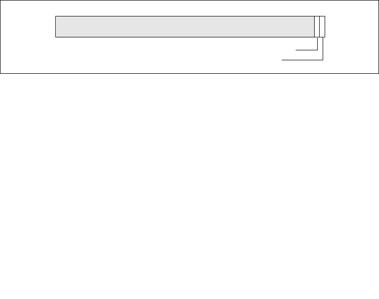
13-8 Vol. 3A
POWER AND THERMAL MANAGEMENT
•If TM1 is enabled and the TCC is engaged, the performance state transition can commence
before the TCC is disengaged.
•If TM2 is enabled and the TCC is engaged, the performance state transition specified by a
write to the IA32_PERF_CTL will commence after the TCC has disengaged.
13.4.2.5 Thermal Status Information
The status of the temperature sensor that triggers the thermal monitor (TM1/TM2) is indicated
through the thermal status flag and thermal status log flag in the IA32_THERM_STATUS MSR
(see Figure 13-5).
The functions of these flags are:
•Thermal Status flag, bit 0 — When set, indicates that the processor core temperature is
currently at the trip temperature of the thermal monitor and that the processor power
consumption is being reduced via either TM1 or TM2, depending on which is enabled.
When clear, the flag indicates that the core temperature is below the thermal monitor trip
temperature. This flag is read only.
•Thermal Status Log flag, bit 1 — When set, indicates that the thermal sensor has tripped
since the last power-up or reset or since the last time that software cleared this flag. This
flag is a sticky bit; once set it remains set until cleared by software or until a power-up or
reset of the processor. The default state is clear.
After the second temperature sensor has been tripped, the thermal monitor (TM1/TM2) will
remain engaged for a minimum time period (on the order of 1 ms). The thermal monitor will
remain engaged until the processor core temperature drops below the preset trip temperature of
the temperature sensor, taking hysteresis into account.
While the processor is in a stop-clock state, interrupts will be blocked from interrupting the
processor. This holding off of interrupts increases the interrupt latency, but does not cause inter-
rupts to be lost. Outstanding interrupts remain pending until clock modulation is complete.
The thermal monitor can be programmed to generate an interrupt to the processor when the
thermal sensor is tripped. The delivery mode, mask and vector for this interrupt can be
programmed through the thermal entry in the local APIC’s LVT (see Section 8.5.1, “Local Vector
Table”). The low-temperature interrupt enable and high-temperature interrupt enable flags in the
IA32_THERM_INTERRUPT MSR (see Figure 13-6) control when the interrupt is generated;
that is, on a transition from a temperature below the trip point to above and/or vice-versa.
Figure 13-5. IA32_THERM_STATUS MSR
63 0
Reserved
12
Thermal Status
Thermal Status Log
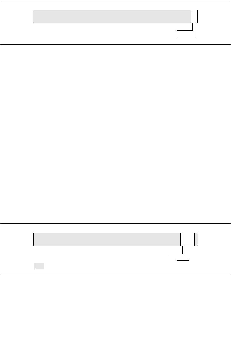
Vol. 3A 13-9
POWER AND THERMAL MANAGEMENT
•High-Temperature Interrupt Enable flag, bit 0 — Enables an interrupt to be generated
on the transition from a low-temperature to a high-temperature when set; disables the
interrupt when clear.(R/W).
•Low-Temperature Interrupt Enable flag, bit 1 — Enables an interrupt to be generated
on the transition from a high-temperature to a low-temperature when set; disables the
interrupt when clear.
The thermal monitor interrupt can be masked by the thermal LVT entry. After a power-up or
reset, the low-temperature interrupt enable and high-temperature interrupt enable flags in the
IA32_THERM_INTERRUPT MSR are cleared (interrupts are disabled) and the thermal LVT
entry is set to mask interrupts. This interrupt should be handled either by the operating system
or system management mode (SMM) code.
Note that the operation of the thermal monitoring mechanism has no effect upon the clock rate
of the processor's internal high-resolution timer (time stamp counter).
13.4.3 Software Controlled Clock Modulation
Pentium 4, Intel Xeon and Pentium M processors also support software-controlled clock modu-
lation. This provides a means for operating systems to implement a power management policy
to reduce the power consumption of the processor. Here, the stop-clock duty cycle is controlled
by software through the IA32_CLOCK_MODULATION MSR (see Figure 13-7).
Figure 13-6. IA32_THERM_INTERRUPT MSR
Figure 13-7. IA32_CLOCK_MODULATION MSR
63 0
Reserved
12
High-Temperature Interrupt Enable
Low-Temperature Interrupt Enable
63 0
Reserved
13
On-Demand Clock Modulation Duty Cycle
On-Demand Clock Modulation Enable
45
Reserved

13-10 Vol. 3A
POWER AND THERMAL MANAGEMENT
The IA32_CLOCK_MODULATION MSR contains the following flag and field used to enable
software-controlled clock modulation and to select the clock modulation duty cycle:
•On-Demand Clock Modulation Enable, bit 4 — Enables on-demand software controlled
clock modulation when set; disables software-controlled clock modulation when clear.
•On-Demand Clock Modulation Duty Cycle, bits 1 through 3 — Selects the on-demand
clock modulation duty cycle (see Table 13-1). This field is only active when the on-
demand clock modulation enable flag is set.
Note that the on-demand clock modulation mechanism (like the thermal monitor) controls the
processor’s stop-clock circuitry internally to modulate the clock signal. The STPCLK# pin is not
used in this mechanism.
The on-demand clock modulation mechanism can be used to control processor power consump-
tion. Power management software can write to the IA32_CLOCK_MODULATION MSR to
enable clock modulation and to select a modulation duty cycle. If on-demand clock modulation
and TM1 are both enabled and the thermal status of the processor is hot (bit 0 of the
IA32_THERM_STATUS MSR is set), clock modulation at the duty cycle specified by TM1
takes precedence, regardless of the setting of the on-demand clock modulation duty cycle.
For Hyper-Threading Technology enabled processors, the IA32_CLOCK_MODULATION
register is duplicated for each logical processor. In order for the On-demand clock modulation
feature to work properly, the feature must be enabled on all the logical processors within a phys-
ical processor. If the programmed duty cycle is not identical for all the logical processors, the
processor clock will modulate to the highest duty cycle programmed.
For the P6 family processors, on-demand clock modulation was implemented through the
chipset, which controlled clock modulation through the processor’s STPCLK# pin.
Table 13-1. On-Demand Clock Modulation Duty Cycle Field Encoding
Duty Cycle Field Encoding Duty Cycle
000B Reserved
001B 12.5% (Default)
010B 25.0%
011B 37.5%
100B 50.0%
101B 63.5%
110B 75%
111B 87.5%

Vol. 3A 13-11
POWER AND THERMAL MANAGEMENT
13.4.4 Detection of Thermal Monitor and Software Controlled
Clock Modulation Facilities
The ACPI flag (bit 22) of the CPUID feature flags indicates the presence of the
IA32_THERM_STATUS, IA32_THERM_INTERRUPT, IA32_CLOCK_MODULATION
MSRs, and the xAPIC thermal LVT entry.
The TM1 flag (bit 29) of the CPUID feature flags indicates the presence of the automatic thermal
monitoring facilities that modulate clock duty cycles.
13.4.5 On Die Digital Thermal Sensors
On die digital thermal sensor can be read using an MSR (no I/O interface). In Intel Core Duo
processors, each core has a unique digital sensor whose temperature is accessible using an MSR.
The digital thermal sensor is the preferred method for reading the die temperature because (a) it
is located closer to the hottest portions of the die, (b) it enables software to accurately track the
die temperature and the potential activation of thermal throttling.
13.4.5.1 Digital Thermal Sensor Enumeration
The processor supports a digital thermal sensor if CPUID.06H.EAX[0] = 1. If the processor
supports digital thermal sensor, EBX[bits 3:0] determine the number of thermal thresholds that
are available for use.
Software sets thermal thresholds by using the IA32_THERM_INTERRUPT MSR. Software
reads output of the digital thermal sensor using the IA32_THERM_STATUS MSR.
13.4.5.2 Reading the Digital Sensor
Unlike traditional analog thermal devices, the output of the digital thermal sensor is a tempera-
ture relative to the maximum supported operating temperature of the processor ( Tj(Max), as
specified in the processor’s data sheet). It is software’s responsibility to convert the relative
temperature to an absolute temperature.
Temperature measurements returned by digital thermal sensors are always at or below Tj(Max).
Over temperature conditions are detected using the out-of-spec status bit. When this bit is set,
the processor is operating out of specification and immediate shutdown of the system should
occur. Once the out-of-spec status bit is set, reliable operation is not guaranteed.
See Figure 13-8 for the layout of IA32_THERM_STATUS MSR. Bit fields include:
•Thermal Status (bit 0, RO) — This bit indicates whether the digital thermal sensor high-
temperature output signal (PROCHOT#) is currently active. Bit 0 = 1 indicates the feature
is active. This bit may not be written by software; it reflects the state of the digital thermal
sensor.
•Thermal Status Log (bit 1, R/WC0) — This is a sticky bit that indicates the history of the
thermal sensor high temperature output signal (PROCHOT#). Bit 1 = 1 if PROCHOT# has
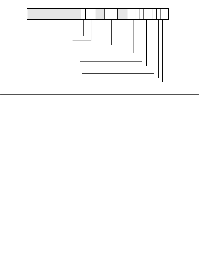
13-12 Vol. 3A
POWER AND THERMAL MANAGEMENT
been asserted since a previous RESET or the last time software cleared the bit. Software
may clear this bit by writing a zero.
•PROCHOT# or FORCEPR# Event (bit 2, RO) — Indicates whether PROCHOT# or
FORCEPR# is being asserted. If bit 2 = 1, PROCHOT# or FORCEPR# has been asserted.
•PROCHOT# or FORCEPR# Log (bit3, R/WC0) — Sticky bit that indicates whether
PROCHOT# or FORCEPR# has been asserted since the last clearing of this bit or a reset.
If bit 3 = 1, PROCHOT# or FORCEPR# has been asserted. Software may clear this bit by
writing a zero.
•Out-Of-Spec Status (bit 4, RO) — Indicates whether the overheat detector output signal
is currently active. If bit 4 = 1, the overheat detector output signal is currently active.
•Out-Of-Spec Status Log (bit 5, R/WC0) — Sticky bit that indicates whether the overheat
detector output signal has been asserted since the last clearing of this bit or reset. If
bit 5 = 1, the output signal has been asserted. Software may clear this bit by writing a zero.
•Thermal Threshold #1 Status (bit 6, RO) — Indicates whether the actual temperature is
currently higher than the value set in Thermal Threshold #1. If bit 6 = 0, the actual
temperature is lower. If bit 6 = 0, the actual temperature is greater than or equal to TT#1.
•Thermal Threshold #1 Log (bit 7, R/WC0) — Sticky bit that indicates whether the
Thermal Threshold #1 has been reached since the last clearing of this bit or a reset. If
bit 7 = 1, the Threshold #1 has been reached. Software may clear this bit by writing a zero.
•Thermal Threshold #2 Status (bit 8, RO) — Indicates whether actual temperature is
currently higher than the value set in Thermal Threshold #2. If bit 8 = 0, the actual
temperature is lower. If bit 8 = 0, the actual temperature is greater than or equal to TT#2.
Figure 13-8. IA32_THERM_STATUS Register
63
0
Reserved
15
Reading Valid
12345810
16222327
Resolution in Deg. Celsius
Digital Readout
Thermal Threshold #2 Log
Thermal Threshold #2 Status
Thermal Threshold #1 Log
Thermal Threshold #1 Status
Out of Spec Status Log
679
3132
Out of Spec Status
PROCHOT# or FORCEPR# Log
PROCHOT# or FORCEPR# Event
Thermal Status Log
Thermal Status
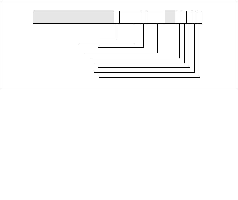
Vol. 3A 13-13
POWER AND THERMAL MANAGEMENT
•Thermal Threshold #2 Log (bit 9, R/WC0) — Sticky bit that indicates whether the
Thermal Threshold #2 has been reached since the last clearing of this bit or a reset. If
bit 9 = 1, the Thermal Threshold #2 has been reached. Software may clear this bit by
writing a zero.
•Digital Readout (bits 22:16, RO) — Digital temperature reading in 1 degree Celsius
relative to Tj(Max). 0 = Tj(Max); 1 = Tj(Max) - 1 oC; etc. See the processor’s data sheet
for details regarding Tj(Max).
•Resolution in Degrees Celsius (bits 30:27, RO) — Specifies the resolution (or tolerance)
of the digital thermal sensor. The value is in degrees Celsius. It is recommended that new
threshold values be offset from the current temperature by at least the resolution + 1 in
order to avoid hysteresis of interrupt generation.
•Reading Valid (bit 31, RO) — Indicates if the digital readout in bits 22:16 is valid. The
readout is valid if bit 31 = 1.
Changes to temperature can be detected using two thresholds (see Figure 13-9); one is set above
and the other below the current temperature. These thresholds have the capability of generating
interrupts using the core's local APIC which software must then service. Note that the local
APIC entries used by these thresholds are also used by the Intel® Thermal Monitor; it is up to
software to determine the source of a specific interrupt.
See Figure 13-9 for the layout of IA32_THERM_INTERRUPT MSR. Bit fields include:
•High-Temperature Interrupt Enable (bit 0, R/W) — This bit allows the BIOS to enable
the generation of an interrupt on the transition from low-temperature to a high-temperature
threshold. Bit 0 = 0 (default) disables interrupts; bit 0 = 1 enables interrupts.
•Low-Temperature Interrupt Enable (bit 1, R/W) — This bit allows the BIOS to enable
the generation of an interrupt on the transition from high-temperature to a low-temper-
ature. Bit 0 = 0 (default) disables interrupts; bit 0 = 1 enables interrupts.
Figure 13-9. IA32_THERM_INTERRUPT Register
63
0
Reserved
15
Threshold #2 Interrupt Enable
12345814
16222324
Threshold #2 Value
Threshold #1 Interrupt Enable
Threshold #1 Value
Overheat Interrupt Enable
FORCPR# Interrupt Enable
THERMTRIP Interrupt Enable
Low Temp. Interrupt Enable
High Temp. Interrupt Enable

13-14 Vol. 3A
POWER AND THERMAL MANAGEMENT
•THERMTRIP# Interrupt Enable (bit 2, R/W) — When a catastrophic cooling failure
occurs, the processor will automatically shutdown. Bit 2 = 0 disables the feature; bit 2 = 1
enables the feature.
•FORCPR# Interrupt Enable (bit 3, R/W) — When a source external to the processor
asserts PROCHOT#, the processor will throttle. Bit 3 = 0 disables the feature; bit 3 = 1
enables the feature.
•Overheat Interrupt Enable (bit 4, R/W) — Enables the generation of an interrupt when
an overheat temperature [>Tj(Max)] is reached. Bit 4 = 0 disables the feature; bit 4 = 1
enables the feature.
•Threshold #1 Value (bits 14:8, R/W) — A temperature relative to Tj(Max) used to
generate an interrupt when the Threshold #1 Interrupt Enable bit is set and the actual
relative temperature reaches or crosses this value.
•Threshold #1 Interrupt Enable (bit 15, R/W) — Enables the generation of an interrupt
when the actual temperature relative to Tj(Max) reaches the value specified in Threshold
#1 value. Bit 15 = 0 disables the feature; bit 15 = 1 enables the feature.
•Threshold #2 Value (bits 22:16, R/W) — A temperature relative to Tj(Max) used to
generate an interrupt when the Threshold #2 Interrupt Enable bit is set and the actual
relative temperature reaches or crosses this value.
•Threshold #2 Interrupt Enable (bit 23, R/W) — Enables the generation of an interrupt
when the actual temperature relative to Tj(Max) reaches the value specified in Threshold
#2 value. Bit 23 = 0 disables the feature; bit 23 = 1 enables the feature.

14
Machine Check
Architecture

Vol. 3A 14-1
CHAPTER 14
MACHINE-CHECK ARCHITECTURE
This chapter describes the machine-check architecture and machine-check exception mecha-
nism found in the Pentium 4, Intel Xeon, and P6 family processors. See Chapter 5, “Interrupt
18—Machine-Check Exception (#MC),” for more information on machine-check exceptions. A
brief description of the Pentium processor’s machine check capability is also given.
14.1 MACHINE-CHECK EXCEPTIONS AND ARCHITECTURE
The Pentium 4, Intel Xeon, and P6 family processors implement a machine-check architecture
that provides a mechanism for detecting and reporting hardware (machine) errors, such as:
system bus errors, ECC errors, parity errors, cache errors, and TLB errors. It consists of a set of
model-specific registers (MSRs) that are used to set up machine checking and additional banks
of MSRs used for recording errors that are detected.
The processor signals the detection of a machine-check error by generating a machine-check
exception (#MC), which is an abort class exception. The implementation of the machine-check
architecture does not ordinarily permit the processor to be restarted reliably after generating a
machine-check exception. However, the machine-check-exception handler can collect informa-
tion about the machine-check error from the machine-check MSRs.
14.2 COMPATIBILITY WITH PENTIUM PROCESSOR
The Pentium 4, Intel Xeon, and P6 family processors support and extend the machine-check
exception mechanism introduced in the Pentium processor. The Pentium processor reports the
following machine-check errors:
•data parity errors during read cycles
•unsuccessful completion of a bus cycle
The above errors are reported using the P5_MC_TYPE and P5_MC_ADDR MSRs (implemen-
tation specific for the Pentium processor). Use the RDMSR instruction to read these MSRs. See
Appendix B, “Model-Specific Registers (MSRs),” for the addresses.
The machine-check error reporting mechanism that Pentium processors use is similar to that
used in Pentium 4, Intel Xeon, and P6 family processors. When an error is detected, it is
recorded in P5_MC_TYPE and P5_MC_ADDR; the processor then generates a machine-check
exception (#MC).
See Section 14.3.3, “Mapping of the Pentium Processor Machine-Check Errors to the Machine-
Check Architecture,” and Section 14.7.3, “Pentium Processor Machine-Check Exception
Handling,” for information on compatibility between machine-check code written to run on the
Pentium processors and code written to run on P6 family processors.

14-2 Vol. 3A
MACHINE-CHECK ARCHITECTURE
14.3 MACHINE-CHECK MSRS
Machine check MSRs in the Pentium 4, Intel Xeon, and P6 family processors consist of a set of
global control and status registers and several error-reporting register banks (see Figure 14-1).
Each error-reporting bank is associated with a specific hardware unit (or group of hardware
units) in the processor. Use RDMSR and WRMSR to read and to write these registers.
14.3.1 Machine-Check Global Control MSRs
The machine-check global control MSRs include the IA32_MCG_CAP, IA32_MCG_STATUS,
and IA32_MCG_CTL. See Appendix B, “Model-Specific Registers (MSRs),” for the addresses
of these registers.
The structure of the IA32_MCG_CAP is implemented differently in Pentium 4 and Intel Xeon
processors and in P6 family processors. Also, note that the register names used for P6 family
processors do not have the ‘IA32’ prefix.
14.3.1.1 IA32_MCG_CAP MSR (Pentium 4 and Intel Xeon Processors)
The IA32_MCG_CAP MSR is a read-only register that provides information about the
machine-check architecture implementation in Pentium 4 and Intel Xeon processors (see
Figure 14-2).
Figure 14-1. Machine-Check MSRs
0
63 0
63
IA32_MCG_CAP MSR
IA32_MCG_STATUS MSR
Error-Reporting Bank Registers
0
63 0
63
IA32_MCi_CTL MSR
IA32_MCi_STATUS MSR
0
63 0
63
IA32_MCi_ADDR MSR
IA32_MCi_MISC MSR
Global Control MSRs (One Set for Each Hardware Unit)
0
63
IA32_MCG_CTL MSR
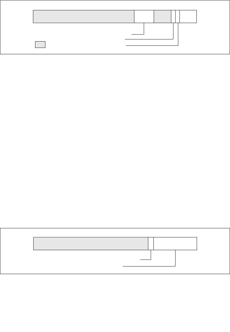
Vol. 3A 14-3
MACHINE-CHECK ARCHITECTURE
Where:
•Count field, bits 0 through 7 — Indicates the number of hardware unit error-reporting
banks available in a particular processor implementation.
•MCG_CTL_P (control MSR present) flag, bit 8 — Indicates that the processor
implements the IA32_MCG_CTL MSR when set; this register is absent when clear.
•MCG_EXT_P (extended MSRs present) flag, bit 9 — Indicates that the processor
implements the extended machine-check state registers found starting at MSR address
180H; these registers are absent when clear.
•MCG_EXT_CNT, bits 16 through 23 — Indicates the number of extended machine-
check state registers present. This field is meaningful only when the MCG_EXT_P flag is
set.
Bits 15-10 and 63-24 are reserved. The effect of writing to the IA32_MCG_CAP register is
undefined.
14.3.1.2 MCG_CAP MSR (P6 Family Processors)
The MCG_CAP MSR is a read-only register that provides information about the machine-check
architecture implementation in P6 family processors (see Figure 14-3).
Figure 14-2. IA32_MCG_CAP Register
Figure 14-3. MCG_CAP Register
MCG_CTL_P
63 0
Reserved
7
Count
891015162324
MCG_EXT_P
MCG_EXT_CNT
Reserved
Count—Number of reporting banks
MCG_CTL_P—MCG_CTL register present
63 0
Reserved
7
Count
89
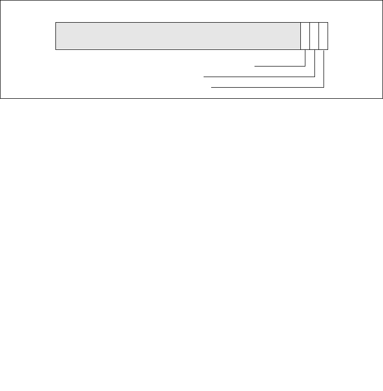
14-4 Vol. 3A
MACHINE-CHECK ARCHITECTURE
Where:
•Count field, bits 0 through 7 — Indicates the number of hardware unit error-reporting
banks available in a particular processor implementation.
•MCG_CTL_P (register present) flag, bit 8 — Indicates that the MCG_CTL register is
present when set and absent when clear.
Bits 9 through 63 are reserved. The effect of writing to the MCG_CAP register is undefined.
14.3.1.3 IA32_MCG_STATUS MSR
The IA32_MCG_STATUS MSR (called the MCG_STATUS MSR for P6 family processors)
describes the current state of the processor after a machine-check exception has occurred (see
Figure 14-4).
Where:
•RIPV (restart IP valid) flag, bit 0 — Indicates (when set) that program execution can be
restarted reliably at the instruction pointed to by the instruction pointer pushed on the stack
when the machine-check exception is generated. When clear, the program cannot be
reliably restarted at the pushed instruction pointer.
•EIPV (error IP valid) flag, bit 1 — Indicates (when set) that the instruction pointed to by
the instruction pointer pushed onto the stack when the machine-check exception is
generated is directly associated with the error. When this flag is cleared, the instruction
pointed to may not be associated with the error.
•MCIP (machine check in progress) flag, bit 2 — Indicates (when set) that a machine-
check exception was generated. Software can set or clear this flag. The occurrence of a
second Machine-Check Event while MCIP is set will cause the processor to enter a
shutdown state. For information on processor behavior in the shutdown state, please refer
to the description in Chapter 5, “Interrupt and Exception Handling”: “Interrupt 8—Double
Fault Exception (#DF)”.
Bits 63-03 in IA32_MCG_STATUS are reserved.
Figure 14-4. IA32_MCG_STATUS Register
EIPV—Error IP valid flag
MCIP—Machine check in progress flag
63 0
Reserved
123
E
I
P
V
M
C
I
P
R
I
P
V
RIPV—Restart IP valid flag
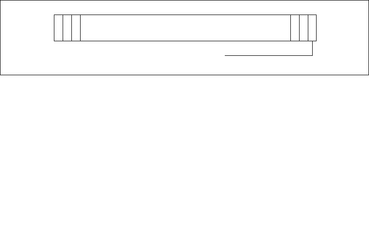
Vol. 3A 14-5
MACHINE-CHECK ARCHITECTURE
14.3.1.4 IA32_MCG_CTL MSR
The IA32_MCG_CTL MSR (called the MCG_CTL MSR in P6 family processors) is present if
the capability flag MCG_CTL_P is set in the IA32_MCG_CAP MSR (or the MCG_CAP MSR).
IA32_MCG_CTL (or MCG_CTL) controls the reporting of machine-check exceptions. If
present, writing 1s to this register enables machine-check features and writing all 0s disables
machine-check features. All other values are undefined and/or implementation specific.
14.3.2 Error-Reporting Register Banks
Each error-reporting register bank can contain the IA32_MCi_CTL, IA32_MCi_STATUS,
IA32_MCi_ADDR, and IA32_MCi_MISC MSRs (called MCi_CTL, MCi_STATUS,
MCi_ADDR, and MCi_MISC in P6 family processors). The Pentium 4 and Intel Xeon proces-
sors provide four or five banks; the P6 family processors provide five banks. The first error-
reporting register (IA32_MC0_CTL) always starts at address 400H.
See Appendix B, “Model-Specific Registers (MSRs),” for addresses of the error-reporting regis-
ters in the Pentium 4 and Intel Xeon processors; and for addresses of the error-reporting registers
P6 family processors.
14.3.2.1 IA32_MCi_CTL MSRs
The IA32_MCi_CTL MSR (called MCi_CTL in P6 family processors) controls error reporting
for errors produced by a particular hardware unit (or group of hardware units). Each of the 64
flags (EEj) represents a potential error. Setting an EEj flag enables reporting of the associated
error and clearing it disables reporting of the error. The processor does not write changes to bits
that are not implemented. Figure 14-5 shows the bit fields of IA32_MCi_CTL.
NOTE
For P6 family processors only: the operating system or executive software
must not modify the contents of the MC0_CTL MSR. This MSR is internally
aliased to the EBL_CR_POWERON MSR and controls platform-specific
error handling features. System specific firmware (the BIOS) is responsible
for the appropriate initialization of the MC0_CTL MSR. P6 family
processors only allow the writing of all 1s or all 0s to the MCi_CTL MSR.
Figure 14-5. IA32_MCi_CTL Register
EEj—Error reporting enable flag
63 0
123
E
E
0
1
E
E
0
2
E
E
0
0
E
E
6
1
E
E
6
2
E
E
6
3
62 61 . . . . .
(where j is 00 through 63)
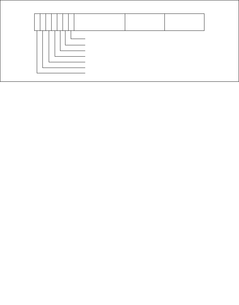
14-6 Vol. 3A
MACHINE-CHECK ARCHITECTURE
14.3.2.2 IA32_MCi_STATUS MSRs
Each IA32_MCi_STATUS MSR (called MCi_STATUS in P6 family processors) contains infor-
mation related to a machine-check error if its VAL (valid) flag is set (see Figure 14-6). Software
is responsible for clearing IA32_MCi_STATUS MSRs by explicitly writing 0s to them; writing
1s to them causes a general-protection exception.
Where:
•MCA (machine-check architecture) error code field, bits 0 through 15 — Specifies the
machine-check architecture-defined error code for the machine-check error condition
detected. The machine-check architecture-defined error codes are guaranteed to be the
same for all IA-32 processors that implement the machine-check architecture. See Section
14.6., “Interpreting the MCA Error Codes,” and Appendix E, “Interpreting Machine-
Check Error Codes,” for information on machine-check error codes.
•Model-specific error code field, bits 16 through 31 — Specifies the model-specific error
code that uniquely identifies the machine-check error condition detected. The model-
specific error codes may differ among IA-32 processors for the same machine-check error
condition. See Appendix E, “Interpreting Machine-Check Error Codes,” for information
on model-specific error codes.
•Other information field, bits 32 through 56 — The functions of these bits are implemen-
tation specific and are not part of the machine-check architecture. Software that is intended
to be portable among IA-32 processors should not rely on these values.
•PCC (processor context corrupt) flag, bit 57 — Indicates (when set) that the state of the
processor might have been corrupted by the error condition detected and that reliable
restarting of the processor may not be possible. When clear, this flag indicates that the
error did not affect the processor’s state.
•ADDRV (IA32_MCi_ADDR register valid) flag, bit 58 — Indicates (when set) that the
IA32_MCi_ADDR register contains the address where the error occurred (see Section
14.3.2.3, “IA32_MCi_ADDR MSRs”). When clear, this flag indicates that the
IA32_MCi_ADDR register is either not implemented or does not contain the address
Figure 14-6. IA32_MCi_STATUS Register
PCC—Processor context corrupt
63 062 6160 59 58 5756 32 31 16 15
VOU
CE
N
P
C
COther Information Model-Specific MCA Error Code
Error Code
ADDRV—MCi_ADDR register valid
MISCV—MCi_MISC register valid
EN—Error enabled
UC—Uncorrected error
OVER—Error overflow
VAL—MCi_STATUS register valid
A
L

Vol. 3A 14-7
MACHINE-CHECK ARCHITECTURE
where the error occurred. Do not read these registers if they are not implemented in the
processor.
•MISCV (IA32_MCi_MISC register valid) flag, bit 59 — Indicates (when set) that the
IA32_MCi_MISC register contains additional information regarding the error. When clear,
this flag indicates that the IA32_MCi_MISC register is either not implemented or does not
contain additional information regarding the error. Do not read these registers if they are
not implemented in the processor.
•EN (error enabled) flag, bit 60 — Indicates (when set) that the error was enabled by the
associated EEj bit of the IA32_MCi_CTL register.
•UC (error uncorrected) flag, bit 61 — Indicates (when set) that the processor did not or
was not able to correct the error condition. When clear, this flag indicates that the
processor was able to correct the error condition.
•OVER (machine check overflow) flag, bit 62 — Indicates (when set) that a machine-
check error occurred while the results of a previous error were still in the error-reporting
register bank (that is, the VAL bit was already set in the IA32_MCi_STATUS register).
The processor sets the OVER flag and software is responsible for clearing it. Enabled
errors are written over disabled errors, and uncorrected errors are written over corrected
errors. Uncorrected errors are not written over previous valid uncorrected errors.
•VAL (IA32_MCi_STATUS register valid) flag, bit 63 — Indicates (when set) that the
information within the IA32_MCi_STATUS register is valid. When this flag is set, the
processor follows the rules given for the OVER flag in the IA32_MCi_STATUS register
when overwriting previously valid entries. The processor sets the VAL flag and software is
responsible for clearing it.
14.3.2.3 IA32_MCi_ADDR MSRs
The IA32_MCi_ADDR MSR (called MCi_ADDR in the P6 family processors) contains the
address of the code or data memory location that produced the machine-check error if the
ADDRV flag in the IA32_MCi_STATUS register is set (see Section 14-7, “IA32_MCi_ADDR
MSR”). The IA32_MCi_ADDR register is either not implemented or contains no address if the
ADDRV flag in the IA32_MCi_STATUS register is clear. When not implemented in the
processor, all reads and writes to this MSR will cause a general protection exception.
The address returned is an offset into a segment, linear address, or physical address. This
depends on the error encountered. These registers can be cleared by explicitly writing 0s to bits
that are not reserved. Writing 1s to these registers will cause a general-protection exception. See
Figure 14-7.

14-8 Vol. 3A
MACHINE-CHECK ARCHITECTURE
14.3.2.4 IA32_MCi_MISC MSRs
The IA32_MCi_MISC MSR (called the MCi_MISC MSR in the P6 family processors) contains
additional information describing the machine-check error if the MISCV flag in the
IA32_MCi_STATUS register is set. The IA32_MCi_MISC_MSR is either not implemented or
does not contain additional information if the MISCV flag in the IA32_MCi_STATUS register
is clear.
When not implemented in the processor, all reads and writes to this MSR will cause a general
protection exception. When implemented in a processor, these registers can be cleared by
explicitly writing all 0s to them; writing 1s to them causes a general-protection exception to be
generated. This register is not implemented in any of the error-reporting register banks for the
P6 family processors.
14.3.2.5 IA32_MCG Extended Machine Check State MSRs
The Pentium 4 and Intel Xeon processors implement a variable number of extended machine-
check state MSRs. The MCG_EXT_P flag in the IA32_MCG_CAP MSR indicates the presence
of these extended registers, and the MCG_EXT_CNT field indicates the number of these regis-
ters actually implemented. See Section 14.3.1.1, “IA32_MCG_CAP MSR (Pentium 4 and Intel
Xeon Processors).” See Table 14-1.
Figure 14-7. IA32_MCi_ADDR MSR
Table 14-1. Extended Machine Check State MSRs
in Processors Without Support for EM64T
MSR Address Description
IA32_MCG_EAX 180H Contains state of the EAX register at the time of the machine-
check error.
IA32_MCG_EBX 181H Contains state of the EBX register at the time of the machine-
check error.
Address
63 0
Reserved
35
36
Address*
63 0
Processor Without Support For Intel EM64T
Processor With Support for Intel EM64T
* Useful bits in this field depend on the address methodology in use when the
the register state is saved.

Vol. 3A 14-9
MACHINE-CHECK ARCHITECTURE
In processors with support for Intel EM64T, 64-bit machine check state MSRs are aliased to the
legacy MSRs. In addition, there may be registers beyond IA32_MCG_MISC. These may
include up to five reserved MSRs (IA32_MCG_RESERVED[1:5]) and save-state MSRs for
registers introduced in 64-bit mode. See Table 14-2.
IA32_MCG_ECX 182H Contains state of the ECX register at the time of the machine-
check error.
IA32_MCG_EDX 183H Contains state of the EDX register at the time of the machine-
check error.
IA32_MCG_ESI 184H Contains state of the ESI register at the time of the machine-
check error.
IA32_MCG_EDI 185H Contains state of the EDI register at the time of the machine-
check error.
IA32_MCG_EBP 186H Contains state of the EBP register at the time of the machine-
check error.
IA32_MCG_ESP 187H Contains state of the ESP register at the time of the machine-
check error.
IA32_MCG_EFLAGS 188H Contains state of the EFLAGS register at the time of the machine-
check error.
IA32_MCG_EIP 189H Contains state of the EIP register at the time of the machine-
check error.
IA32_MCG_MISC 18AH When set, indicates that a page assist or page fault occurred
during DS normal operation.
Table 14-2. Extended Machine Check State MSRs
In Processors With Support For Intel EM64T
MSR Address Description
IA32_MCG_RAX 180H Contains state of the RAX register at the time of the machine-check
error.
IA32_MCG_RBX 181H Contains state of the RBX register at the time of the machine-check
error.
IA32_MCG_RCX 182H Contains state of the RCX register at the time of the machine-check
error.
IA32_MCG_RDX 183H Contains state of the RDX register at the time of the machine-check
error.
IA32_MCG_RSI 184H Contains state of the RSI register at the time of the machine-check
error.
IA32_MCG_RDI 185H Contains state of the RDI register at the time of the machine-check
error.
Table 14-1. Extended Machine Check State MSRs
in Processors Without Support for EM64T (Contd.)
MSR Address Description

14-10 Vol. 3A
MACHINE-CHECK ARCHITECTURE
When a machine-check error is detected on a Pentium 4 or Intel Xeon processor, the processor
saves the state of the general-purpose registers, the R/EFLAGS register, and the R/EIP in these
extended machine-check state MSRs. This information can be used by a debugger to analyze the
error.
These registers are read/write to zero registers. This means software can read them; but if soft-
ware writes to them, only all zeros is allowed. If software attempts to write a non-zero value into
one of these registers, a general-protection (#GP) exception is generated. These registers are
cleared on a hardware reset (power-up or RESET), but maintain their contents following a soft
reset (INIT reset).
IA32_MCG_RBP 186H Contains state of the RBP register at the time of the machine-check
error.
IA32_MCG_RSP 187H Contains state of the RSP register at the time of the machine-check
error.
IA32_MCG_RFLAGS 188H Contains state of the RFLAGS register at the time of the machine-
check error.
IA32_MCG_RIP 189H Contains state of the RIP register at the time of the machine-check
error.
IA32_MCG_MISC 18AH When set, indicates that a page assist or page fault occurred during
DS normal operation.
IA32_MCG_
RSERVED[1:5] 18BH-
18FH These registers, if present, are reserved.
IA32_MCG_R8 190H Contains state of the R8 register at the time of the machine-check
error.
IA32_MCG_R9 191H Contains state of the R9 register at the time of the machine-check
error.
IA32_MCG_R10 192H Contains state of the R10 register at the time of the machine-check
error.
IA32_MCG_R11 193H Contains state of the R11 register at the time of the machine-check
error.
IA32_MCG_R12 194H Contains state of the R12 register at the time of the machine-check
error.
IA32_MCG_R13 194H Contains state of the R8 register at the time of the machine-check
error.
IA32_MCG_R14 196H Contains state of the R14 register at the time of the machine-check
error.
IA32_MCG_R15 197H Contains state of the R15 register at the time of the machine-check
error.
Table 14-2. Extended Machine Check State MSRs
In Processors With Support For Intel EM64T (Contd.)
MSR Address Description

Vol. 3A 14-11
MACHINE-CHECK ARCHITECTURE
14.3.3 Mapping of the Pentium Processor Machine-Check Errors
to the Machine-Check Architecture
The Pentium processor reports machine-check errors using two registers: P5_MC_TYPE and
P5_MC_ADDR. The Pentium 4, Intel Xeon, and P6 family processors map these registers to the
IA32_MCi_STATUS and IA32_MCi_ADDR in the error-reporting register bank. This bank
reports on the same type of external bus errors reported in P5_MC_TYPE and P5_MC_ADDR.
The information in these registers can then be accessed in two ways:
•By reading the IA32_MCi_STATUS and IA32_MCi_ADDR registers as part of a general
machine-check exception handler written for Pentium 4 and P6 family processors.
•By reading the P5_MC_TYPE and P5_MC_ADDR registers using the RDMSR
instruction.
The second capability permits a machine-check exception handler written to run on a Pentium
processor to be run on a Pentium 4, Intel Xeon, or P6 family processor. There is a limitation in
that information returned by the Pentium 4, Intel Xeon, and P6 family processors is encoded
differently than information returned by the Pentium processor. To run a Pentium processor
machine-check exception handler on a Pentium 4, Intel Xeon, or P6 family processor; the
handler must be written to interpret P5_MC_TYPE encodings correctly.
14.4 MACHINE-CHECK AVAILABILITY
The machine-check architecture and machine-check exception (#MC) are model-specific
features. Software can execute the CPUID instruction to determine whether a processor imple-
ments these features. Following the execution of the CPUID instruction, the settings of the MCA
flag (bit 14) and MCE flag (bit 7) in EDX indicate whether the processor implements the
machine-check architecture and machine-check exception.
14.5 MACHINE-CHECK INITIALIZATION
To use the processors machine-check architecture, software must initialize the processor to acti-
vate the machine-check exception and the error-reporting mechanism.
Example 14-19 gives pseudocode for performing this initialization. This pseudocode checks for
the existence of the machine-check architecture and exception; it then enables machine-check
exception and the error-reporting register banks. The pseudocode shown is compatible with the
Pentium 4, Intel Xeon, P6 family, and Pentium processors.
Following power up or power cycling, IA32_MCi_STATUS registers are not guaranteed to have
valid data until after they are initially cleared to zero by software (as shown in the initialization
pseudocode in Example 14-19). In addition, when using P6 family processors, software must set
MCi_STATUS registers to zero when doing a soft-reset.

14-12 Vol. 3A
MACHINE-CHECK ARCHITECTURE
Example 14-19. Machine-Check Initialization Pseudocode
Check CPUID Feature Flags for MCE and MCA support
IF CPU supports MCE
THEN
IF CPU supports MCA
THEN
IF (IA32_MCG_CAP.MCG_CTL_P = 1)
(* IA32_MCG_CTL register is present *)
THEN
IA32_MCG_CTL ← FFFFFFFFFFFFFFFFH;
(* enables all MCA features *)
FI
(* Determine number of error-reporting banks supported *)
COUNT← IA32_MCG_CAP.Count;
MAX_BANK_NUMBER ← COUNT - 1;
IF (Processor Family is 6H)
THEN
(* Enable logging of all errors except for MC0_CTL register *)
FOR error-reporting banks (1 through MAX_BANK_NUMBER)
DO IA32_MCi_CTL ← 0FFFFFFFFFFFFFFFFH;
OD
(* Clear all errors *)
FOR error-reporting banks (0 through MAX_BANK_NUMBER)
DO IA32_MCi_STATUS ← 0;
OD
ELSE IF (Processor Family is 0FH) (*any Processor Extended Family *)
THEN
(* Enable logging of all errors including MC0_CTL register *)
FOR error-reporting banks (0 through MAX_BANK_NUMBER)
DO IA32_MCi_CTL ← 0FFFFFFFFFFFFFFFFH;
OD
(* BIOS clears all errors only on power-on reset *)
IF (BIOS detects Power-on reset)
THEN
FOR error-reporting banks (0 through MAX_BANK_NUMBER)
DO IA32_MCi_STATUS ← 0;
OD
ELSE

Vol. 3A 14-13
MACHINE-CHECK ARCHITECTURE
FOR error-reporting banks (0 through MAX_BANK_NUMBER)
DO (Optional for BIOS and OS) Log valid errors
(OS only) IA32_MCi_STATUS ← 0;
OD
FI
FI
FI
Setup the Machine Check Exception (#MC) handler for vector 18 in IDT
Set the MCE bit (bit 6) in CR4 register to enable Machine-Check Exceptions
FI
14.6. INTERPRETING THE MCA ERROR CODES
When the processor detects a machine-check error condition, it writes a 16-bit error code to the
MCA error code field of one of the IA32_MCi_STATUS registers and sets the VAL (valid) flag
in that register. The processor may also write a 16-bit model-specific error code in the
IA32_MCi_STATUS register depending on the implementation of the machine-check architec-
ture of the processor.
The MCA error codes are architecturally defined for IA-32 processors. However, the specific
IA32_MCi_STATUS register that a code is ‘written to’ is model specific. To determine the cause
of a machine-check exception, the machine-check exception handler must read the VAL flag for
each IA32_MCi_STATUS register. If the flag is set, the machine check-exception handler must
then read the MCA error code field of the register. It is the encoding of the MCA error code field
[15:0] that determines the type of error being reported and not the register bank reporting it.
There are two types of MCA error codes: simple error codes and compound error codes.
14.6.1 Simple Error Codes
Table 14-3 shows the simple error codes. These unique codes indicate global error information.

14-14 Vol. 3A
MACHINE-CHECK ARCHITECTURE
14.6.2 Compound Error Codes
Compound error codes describe errors related to the TLBs, memory, caches, bus and intercon-
nect logic, and internal timer. A set of sub-fields is common to all of compound errors. These
sub-fields describe the type of access, level in the memory hierarchy, and type of request.
Table 14-5 shows the general form of the compound error codes. The interpretation column
indicates the name of a compound error. The name is constructed by substituting mnemonics
from Tables 14-5 through 14-8 for the sub-field names given within curly braces.
Table 14-3. IA32_MCi_Status [15:0] Simple Error Code Encoding
Error Code Binary Encoding Meaning
No Error 0000 0000 0000 0000 No error has been reported to this bank of
error-reporting registers.
Unclassified 0000 0000 0000 0001 This error has not been classified into the
MCA error classes.
Microcode ROM Parity
Error 0000 0000 0000 0010 Parity error in internal microcode ROM
External Error 0000 0000 0000 0011 The BINIT# from another processor caused
this processor to enter machine check.1
FRC Error 0000 0000 0000 0100 FRC (functional redundancy check)
master/slave error
Internal Unclassified 0000 01xx xxxx xxxx Internal unclassified errors 2
NOTES:
1. BINIT# assertion will cause a machine check exception if the processor (or any processor on the same
external bus) has BINIT# observation enabled during power-on configuration (hardware strapping) and
if machine check exceptions are enabled (by setting CR4.MCE = 1).
2. Internal unclassified errors have not been classified. This is because no additional information is
included in the machine check register.
Vol. 3A 14-15
MACHINE-CHECK ARCHITECTURE
For example, the error code ICACHEL1_RD_ERR is constructed from the form:
{TT}CACHE{LL}_{RRRR}_ERR,
where {TT} is replaced by I, {LL} is replaced by L1, and {RRRR} is replaced by RD.
The 2-bit TT sub-field (Table 14-5) indicates the type of transaction (data, instruction, or
generic). The sub-field applies to the TLB, cache, and interconnect error conditions. Note that
interconnect error conditions are primarily associated with P6 family and Pentium processors,
which utilize an external APIC bus separate from the system bus. The generic type is reported
when the processor cannot determine the transaction type.
The 2-bit LL sub-field (see Table 14-6) indicates the level in the memory hierarchy where the
error occurred (level 0, level 1, level 2, or generic). The LL sub-field also applies to the TLB,
cache, and interconnect error conditions. The Pentium 4, Intel Xeon, and P6 family processors
support two levels in the cache hierarchy and one level in the TLBs. Again, the generic type is
reported when the processor cannot determine the hierarchy level.
Table 14-4. IA32_MCi_Status [15:0] Compound Error Code Encoding
Type Form Interpretation
TLB Errors 0000 0000 0001 TTLL {TT}TLB{LL}_ERR
Memory Hierarchy Errors 0000 0001 RRRR TTLL {TT}CACHE{LL}_{RRRR}_ERR
Bus and Interconnect
Errors 0000 1PPT RRRR IILL BUS{LL}_{PP}_{RRRR}_{II}_{T}_ERR
Internal Timer 0000 0100 0000 0000
Table 14-5. Encoding for TT (Transaction Type) Sub-Field
Transaction Type Mnemonic Binary Encoding
Instruction I 00
Data D 01
Generic G 10
Table 14-6. Level Encoding for LL (Memory Hierarchy Level) Sub-Field
Hierarchy Level Mnemonic Binary Encoding
Level 0 L0 00
Level 1 L1 01
Level 2 L2 10
Generic LG 11

14-16 Vol. 3A
MACHINE-CHECK ARCHITECTURE
The 4-bit RRRR sub-field (see Table 14-7) indicates the type of action associated with the error.
Actions include read and write operations, prefetches, cache evictions, and snoops. Generic
error is returned when the type of error cannot be determined. Generic read and generic write
are returned when the processor cannot determine the type of instruction or data request that
caused the error. Eviction and snoop requests apply only to the caches. All of the other requests
apply to TLBs, caches and interconnects.
The bus and interconnect errors are defined with the 2-bit PP (participation), 1-bit T (time-
out), and 2-bit II (memory or I/O) sub-fields, in addition to the LL and RRRR sub-fields (see
Table 14-8). The bus error conditions are implementation dependent and related to the type of
bus implemented by the processor. Likewise, the interconnect error conditions are predicated
on a specific implementation-dependent interconnect model that describes the connections
between the different levels of the storage hierarchy. The type of bus is implementation depen-
dent, and as such is not specified in this document. A bus or interconnect transaction consists
of a request involving an address and a response.
Table 14-7. Encoding of Request (RRRR) Sub-Field
Request Type Mnemonic Binary Encoding
Generic Error ERR 0000
Generic Read RD 0001
Generic Write WR 0010
Data Read DRD 0011
Data Write DWR 0100
Instruction Fetch IRD 0101
Prefetch PREFETCH 0110
Eviction EVICT 0111
Snoop SNOOP 1000

Vol. 3A 14-17
MACHINE-CHECK ARCHITECTURE
14.6.3 Machine-Check Error Codes Interpretation
Appendix E, “Interpreting Machine-Check Error Codes,” provides information on interpreting
the MCA error code, model-specific error code, and other information error code fields. For
P6 family processors, information has been included on decoding external bus errors. For
Pentium 4 and Intel Xeon processors; information is included on external bus, internal timer
and memory hierarchy errors.
14.7 GUIDELINES FOR WRITING MACHINE-CHECK SOFTWARE
The machine-check architecture and error logging can be used in two different ways:
•To detect machine errors during normal instruction execution, using the machine-check
exception (#MC).
•To periodically check and log machine errors.
To use the machine-check exception, the operating system or executive software must provide
a machine-check exception handler. This handler can be designed specifically for Pentium 4 and
Intel Xeon processors or for P6 family processors. It can also be a portable handler that handles
processor machine-check errors from several generations of IA-32 processors.
A special program or utility is required to log machine errors.
Guidelines for writing a machine-check exception handler or a machine-error logging utility are
given in the following sections.
Table 14-8. Encodings of PP, T, and II Sub-Fields
Sub-Field Transaction Mnemonic Binary Encoding
PP (Participation) Local processor1 originated request SRC 00
Local processor1 responded to request RES 01
Local processor1 observed error as third
party OBS 10
Generic 11
T (Time-out) Request timed out TIMEOUT 1
Request did not time out NOTIMEOUT 0
II (Memory or I/O) Memory Access M 00
Reserved 01
I/O IO 10
Other transaction 11
NOTE:
1. Local processor differentiates the processor reporting the error from other system components (includ-
ing the APIC, other processors, etc.).

14-18 Vol. 3A
MACHINE-CHECK ARCHITECTURE
14.7.1 Machine-Check Exception Handler
The machine-check exception (#MC) corresponds to vector 18. To service machine-check
exceptions, a trap gate must be added to the IDT. The pointer in the trap gate must point to a
machine-check exception handler. Two approaches can be taken to designing the exception
handler:
1. The handler can merely log all the machine status and error information, then call a
debugger or shut down the system.
2. The handler can analyze the reported error information and, in some cases, attempt to
correct the error and restart the processor.
For Pentium 4, Intel Xeon, P6 family, and Pentium processors; virtually all machine-check
conditions cannot be corrected (they result in abort-type exceptions). The logging of status and
error information is therefore a baseline implementation requirement.
When recovery from a machine-check error may be possible, consider the following when
writing a machine-check exception handler:
•To determine the nature of the error, the handler must read each of the error-reporting
register banks. The count field in the IA32_MCG_CAP register gives number of register
banks. The first register of register bank 0 is at address 400H.
•The VAL (valid) flag in each IA32_MCi_STATUS register indicates whether the error
information in the register is valid. If this flag is clear, the registers in that bank do not
contain valid error information and do not need to be checked.
•To write a portable exception handler, only the MCA error code field in the
IA32_MCi_STATUS register should be checked. See Section 14.6. for information that
can be used to write an algorithm to interpret this field.
•The RIPV, PCC, and OVER flags in each IA32_MCi_STATUS register indicate whether
recovery from the error is possible. If one of these fields is set, recovery is not possible.
The OVER field indicates that two or more machine-check errors occurred. When
recovery is not possible, the handler typically records the error information and signals an
abort to the operating system.
•Correctable errors are corrected automatically by the processor. The UC flag in each
IA32_MCi_STATUS register indicates whether the processor automatically corrected an
error.
•The RIPV flag in the IA32_MCG_STATUS register indicates whether the program can be
restarted at the instruction indicated by the instruction pointer (the address of the
instruction pushed on the stack when the exception was generated). If this flag is clear, the
processor may still be able to be restarted (for debugging purposes) but not without loss of
program continuity.
•For unrecoverable errors, the EIPV flag in the IA32_MCG_STATUS register indicates
whether the instruction indicated by the instruction pointer pushed on the stack (when the
exception was generated) is related to the error. If the flag is clear, the pushed instruction
may not be related to the error.

Vol. 3A 14-19
MACHINE-CHECK ARCHITECTURE
•The MCIP flag in the IA32_MCG_STATUS register indicates whether a machine-check
exception was generated. Before returning from the machine-check exception handler,
software should clear this flag so that it can be used reliably by an error logging utility. The
MCIP flag also detects recursion. The machine-check architecture does not support
recursion. When the processor detects machine-check recursion, it enters the shutdown
state.
14.7.2 Enabling BINIT# Drive and BINIT# Observation
For complete operation of the processors machine check capabilities, it is essential that the
system BIOS enable BINIT# drive and BINIT# observation. This allows the processor to use
BINIT# to clear internal blocking states and some external blocking states. This also allows the
processor to correctly report a wide range of machine check exceptions.
For example, on a Pentium III processor that is:
•Executing a locked CMPXCHG8B instruction.
•Reports a machine check exception on the initial data read.
•And the comparison operation fails.
The processor unlocks the bus after completion of the locked sequence by asserting a BINIT#
signal. Without BINIT# drive (UP environment) or BINIT# drive and observation enabled (MP
environment); the machine check error is logged but the machine check exception is not taken
(if MCE's are enabled).
Example 14-20 gives typical steps carried out by a machine-check exception handler.
Example 14-20. Machine-Check Exception Handler
Pseudocode
IF CPU supports MCE
THEN
IF CPU supports MCA
THEN
call errorlogging routine; (* returns restartability *)
FI;
ELSE (* Pentium(R) processor compatible *)
READ P5_MC_ADDR
READ P5_MC_TYPE;
report RESTARTABILITY to console;
FI;
IF error is not restartable
THEN
report RESTARTABILITY to console;
abort system;
FI;
CLEAR MCIP flag in IA32_MCG_STATUS;

14-20 Vol. 3A
MACHINE-CHECK ARCHITECTURE
14.7.3 Pentium Processor Machine-Check Exception Handling
To make the machine-check exception handler portable to the Pentium 4, Intel Xeon, P6 family,
and Pentium processors, checks can be made (using CPUID) to determine the processor type.
Then based on the processor type, machine-check exceptions can be handled specifically for
Pentium 4, Intel Xeon, P6 family, or Pentium processors.
When machine-check exceptions are enabled for the Pentium processor (MCE flag is set in
control register CR4), the machine-check exception handler uses the RDMSR instruction to read
the error type from the P5_MC_TYPE register and the machine check address from the
P5_MC_ADDR register. The handler then normally reports these register values to the system
console before aborting execution (see Example 14-20).
14.7.4 Logging Correctable Machine-Check Errors
If a machine-check error is correctable, the processor does not generate a machine-check excep-
tion for it. To detect correctable machine-check errors, a utility program must be written that
reads each of the machine-check error-reporting register banks and logs the results in an
accounting file or data structure. This utility can be implemented in either of the following ways.
•A system daemon that polls the register banks on an infrequent basis, such as hourly or
daily.
•A user-initiated application that polls the register banks and records the exceptions. Here,
the actual polling service is provided by an operating-system driver or through the system
call interface.
Example 14-21 gives pseudocode for an error logging utility.
Example 14-21. Machine-Check Error Logging Pseudocode
Assume that execution is restartable;
IF the processor supports MCA
THEN
FOR each bank of machine-check registers
DO READ IA32_MCi_STATUS;
IF VAL flag in IA32_MCi_STATUS = 1
THEN
IF ADDRV flag in IA32_MCi_STATUS = 1
THEN READ IA32_MCi_ADDR;
FI;
IF MISCV flag in IA32_MCi_STATUS = 1
THEN READ IA32_MCi_MISC;
FI;
IF MCIP flag in IA32_MCG_STATUS = 1
(* Machine-check exception is in progress *)
AND PCC flag in IA32_MCi_STATUS = 1

Vol. 3A 14-21
MACHINE-CHECK ARCHITECTURE
AND RIPV flag in IA32_MCG_STATUS = 0
(* execution is not restartable *)
THEN
RESTARTABILITY = FALSE;
return RESTARTABILITY to calling procedure;
FI;
Save time-stamp counter and processor ID;
Set IA32_MCi_STATUS to all 0s;
Execute serializing instruction (i.e., CPUID);
FI;
OD;
FI;
If the processor supports the machine-check architecture, the utility reads through the banks of
error-reporting registers looking for valid register entries. It then saves the values of the
IA32_MCi_STATUS, IA32_MCi_ADDR, IA32_MCi_MISC and IA32_MCG_STATUS regis-
ters for each bank that is valid. The routine minimizes processing time by recording the raw data
into a system data structure or file, reducing the overhead associated with polling. User utilities
analyze the collected data in an off-line environment.
When the MCIP flag is set in the IA32_MCG_STATUS register, a machine-check exception is
in progress and the machine-check exception handler has called the exception logging routine.
Once the logging process has been completed the exception-handling routine must determine
whether execution can be restarted, which is usually possible when damage has not occurred
(The PCC flag is clear, in the IA32_MCi_STATUS register) and when the processor can guar-
antee that execution is restartable (the RIPV flag is set in the IA32_MCG_STATUS register). If
execution cannot be restarted, the system is not recoverable and the exception-handling routine
should signal the console appropriately before returning the error status to the Operating System
kernel for subsequent shutdown.
The machine-check architecture allows buffering of exceptions from a given error-reporting
bank although the Pentium 4, Intel Xeon, and P6 family processors do not implement this
feature. The error logging routine should provide compatibility with future processors by
reading each hardware error-reporting bank's IA32_MCi_STATUS register and then writing 0s
to clear the OVER and VAL flags in this register. The error logging utility should re-read the
IA32_MCi_STATUS register for the bank ensuring that the valid bit is clear. The processor will
write the next error into the register bank and set the VAL flags.
Additional information that should be stored by the exception-logging routine includes the
processor’s time-stamp counter value, which provides a mechanism to indicate the frequency of
exceptions. A multiprocessing operating system stores the identity of the processor node incur-
ring the exception using a unique identifier, such as the processor’s APIC ID (see Section 8.8,
“Handling Interrupts”).

14-22 Vol. 3A
MACHINE-CHECK ARCHITECTURE
The basic algorithm given in Example 14-21 can be modified to provide more robust recovery
techniques. For example, software has the flexibility to attempt recovery using information
unavailable to the hardware. Specifically, the machine-check exception handler can, after
logging carefully analyze the error-reporting registers when the error-logging routine reports an
error that does not allow execution to be restarted. These recovery techniques can use external
bus related model-specific information provided with the error report to localize the source of
the error within the system and determine the appropriate recovery strategy.

15
8086 Emulation

Vol. 3A 15-1
CHAPTER 15
8086 EMULATION
IA-32 processors (beginning with the Intel386 processor) provide two ways to execute new or
legacy programs that are assembled and/or compiled to run on an Intel 8086 processor:
•Real-address mode.
•Virtual-8086 mode.
Figure 2-3 shows the relationship of these operating modes to protected mode and system
management mode (SMM).
When the processor is powered up or reset, it is placed in the real-address mode. This operating
mode almost exactly duplicates the execution environment of the Intel 8086 processor, with
some extensions. Virtually any program assembled and/or compiled to run on an Intel 8086
processor will run on an IA-32 processor in this mode.
When running in protected mode, the processor can be switched to virtual-8086 mode to run
8086 programs. This mode also duplicates the execution environment of the Intel 8086
processor, with extensions. In virtual-8086 mode, an 8086 program runs as a separate protected-
mode task. Legacy 8086 programs are thus able to run under an operating system (such as
Microsoft Windows*) that takes advantage of protected mode and to use protected-mode facil-
ities, such as the protected-mode interrupt- and exception-handling facilities. Protected-mode
multitasking permits multiple virtual-8086 mode tasks (with each task running a separate 8086
program) to be run on the processor along with other non-virtual-8086 mode tasks.
This section describes both the basic real-address mode execution environment and the virtual-
8086-mode execution environment, available on the IA-32 processors beginning with the
Intel386 processor.
15.1 REAL-ADDRESS MODE
The IA-32 architecture’s real-address mode runs programs written for the Intel 8086, Intel 8088,
Intel 80186, and Intel 80188 processors, or for the real-address mode of the Intel 286, Intel386,
Intel486, Pentium, P6 family, Pentium 4, and Intel Xeon processors.
The execution environment of the processor in real-address mode is designed to duplicate the
execution environment of the Intel 8086 processor. To an 8086 program, a processor operating
in real-address mode behaves like a high-speed 8086 processor. The principal features of this
architecture are defined in Chapter 3, “Basic Execution Environment”, of the IA-32 Intel®
Architecture Software Developer’s Manual, Volume 1.

15-2 Vol. 3A
8086 EMULATION
The following is a summary of the core features of the real-address mode execution environment
as would be seen by a program written for the 8086:
•The processor supports a nominal 1-MByte physical address space (see Section 15.1.1,
“Address Translation in Real-Address Mode”, for specific details). This address space is
divided into segments, each of which can be up to 64 KBytes in length. The base of a
segment is specified with a 16-bit segment selector, which is zero extended to form a
20-bit offset from address 0 in the address space. An operand within a segment is
addressed with a 16-bit offset from the base of the segment. A physical address is thus
formed by adding the offset to the 20-bit segment base (see Section 15.1.1, “Address
Translation in Real-Address Mode”).
•All operands in “native 8086 code” are 8-bit or 16-bit values. (Operand size override
prefixes can be used to access 32-bit operands.)
•Eight 16-bit general-purpose registers are provided: AX, BX, CX, DX, SP, BP, SI, and DI.
The extended 32 bit registers (EAX, EBX, ECX, EDX, ESP, EBP, ESI, and EDI) are
accessible to programs that explicitly perform a size override operation.
•Four segment registers are provided: CS, DS, SS, and ES. (The FS and GS registers are
accessible to programs that explicitly access them.) The CS register contains the segment
selector for the code segment; the DS and ES registers contain segment selectors for data
segments; and the SS register contains the segment selector for the stack segment.
•The 8086 16-bit instruction pointer (IP) is mapped to the lower 16-bits of the EIP register.
Note this register is a 32-bit register and unintentional address wrapping may occur.
•The 16-bit FLAGS register contains status and control flags. (This register is mapped to
the 16 least significant bits of the 32-bit EFLAGS register.)
•All of the Intel 8086 instructions are supported (see Section 15.1.3, “Instructions
Supported in Real-Address Mode”).
•A single, 16-bit-wide stack is provided for handling procedure calls and invocations of
interrupt and exception handlers. This stack is contained in the stack segment identified
with the SS register. The SP (stack pointer) register contains an offset into the stack
segment. The stack grows down (toward lower segment offsets) from the stack pointer.
The BP (base pointer) register also contains an offset into the stack segment that can be
used as a pointer to a parameter list. When a CALL instruction is executed, the processor
pushes the current instruction pointer (the 16 least-significant bits of the EIP register and,
on far calls, the current value of the CS register) onto the stack. On a return, initiated with
a RET instruction, the processor pops the saved instruction pointer from the stack into the
EIP register (and CS register on far returns). When an implicit call to an interrupt or
exception handler is executed, the processor pushes the EIP, CS, and EFLAGS (low-order
16-bits only) registers onto the stack. On a return from an interrupt or exception handler,
initiated with an IRET instruction, the processor pops the saved instruction pointer and
EFLAGS image from the stack into the EIP, CS, and EFLAGS registers.
•A single interrupt table, called the “interrupt vector table” or “interrupt table,” is
provided for handling interrupts and exceptions (see Figure 15-2). The interrupt table
(which has 4-byte entries) takes the place of the interrupt descriptor table (IDT, with

Vol. 3A 15-3
8086 EMULATION
8-byte entries) used when handling protected-mode interrupts and exceptions. Interrupt
and exception vector numbers provide an index to entries in the interrupt table. Each
entry provides a pointer (called a “vector”) to an interrupt- or exception-handling
procedure. See Section 15.1.4, “Interrupt and Exception Handling”, for more details. It is
possible for software to relocate the IDT by means of the LIDT instruction on IA-32
processors beginning with the Intel386 processor.
•The x87 FPU is active and available to execute x87 FPU instructions in real-address mode.
Programs written to run on the Intel 8087 and Intel 287 math coprocessors can be run in
real-address mode without modification.
The following extensions to the Intel 8086 execution environment are available in the IA-32
architecture’s real-address mode. If backwards compatibility to Intel 286 and Intel 8086 proces-
sors is required, these features should not be used in new programs written to run in real-address
mode.
•Two additional segment registers (FS and GS) are available.
•Many of the integer and system instructions that have been added to later IA-32 processors
can be executed in real-address mode (see Section 15.1.3, “Instructions Supported in Real-
Address Mode”).
•The 32-bit operand prefix can be used in real-address mode programs to execute the 32-bit
forms of instructions. This prefix also allows real-address mode programs to use the
processor’s 32-bit general-purpose registers.
•The 32-bit address prefix can be used in real-address mode programs, allowing 32-bit
offsets.
The following sections describe address formation, registers, available instructions, and inter-
rupt and exception handling in real-address mode. For information on I/O in real-address mode,
see Chapter 13, “Input/Output”, of the IA-32 Intel® Architecture Software Developer’s Manual,
Volume 1.
15.1.1 Address Translation in Real-Address Mode
In real-address mode, the processor does not interpret segment selectors as indexes into a
descriptor table; instead, it uses them directly to form linear addresses as the 8086 processor
does. It shifts the segment selector left by 4 bits to form a 20-bit base address (see Figure 15-1).
The offset into a segment is added to the base address to create a linear address that maps directly
to the physical address space.
When using 8086-style address translation, it is possible to specify addresses larger than
1 MByte. For example, with a segment selector value of FFFFH and an offset of FFFFH, the
linear (and physical) address would be 10FFEFH (1 megabyte plus 64 KBytes). The 8086
processor, which can form addresses only up to 20 bits long, truncates the high-order bit, thereby
“wrapping” this address to FFEFH. When operating in real-address mode, however, the
processor does not truncate such an address and uses it as a physical address. (Note, however,
that for IA-32 processors beginning with the Intel486 processor, the A20M# signal can be used
in real-address mode to mask address line A20, thereby mimicking the 20-bit wrap-around

15-4 Vol. 3A
8086 EMULATION
behavior of the 8086 processor.) Care should be take to ensure that A20M# based address wrap-
ping is handled correctly in multiprocessor based system.
The IA-32 processors beginning with the Intel386 processor can generate 32-bit offsets using an
address override prefix; however, in real-address mode, the value of a 32-bit offset may not
exceed FFFFH without causing an exception.
For full compatibility with Intel 286 real-address mode, pseudo-protection faults (interrupt 12
or 13) occur if a 32-bit offset is generated outside the range 0 through FFFFH.
15.1.2 Registers Supported in Real-Address Mode
The register set available in real-address mode includes all the registers defined for the 8086
processor plus the new registers introduced in later IA-32 processors, such as the FS and GS
segment registers, the debug registers, the control registers, and the floating-point unit registers.
The 32-bit operand prefix allows a real-address mode program to use the 32-bit general-purpose
registers (EAX, EBX, ECX, EDX, ESP, EBP, ESI, and EDI).
15.1.3 Instructions Supported in Real-Address Mode
The following instructions make up the core instruction set for the 8086 processor. If backwards
compatibility to the Intel 286 and Intel 8086 processors is required, only these instructions
should be used in a new program written to run in real-address mode.
•Move (MOV) instructions that move operands between general-purpose registers, segment
registers, and between memory and general-purpose registers.
•The exchange (XCHG) instruction.
•Load segment register instructions LDS and LES.
•Arithmetic instructions ADD, ADC, SUB, SBB, MUL, IMUL, DIV, IDIV, INC, DEC,
CMP, and NEG.
Figure 15-1. Real-Address Mode Address Translation
19 0
16-bit Segment Selector
3
0 0 0 0
Base
19 0
16-bit Effective Address
15
0 0 0 0
Offset
0
20-bit Linear Address
Linear
Address
+
=
4
16
19

Vol. 3A 15-5
8086 EMULATION
•Logical instructions AND, OR, XOR, and NOT.
•Decimal instructions DAA, DAS, AAA, AAS, AAM, and AAD.
•Stack instructions PUSH and POP (to general-purpose registers and segment registers).
•Type conversion instructions CWD, CDQ, CBW, and CWDE.
•Shift and rotate instructions SAL, SHL, SHR, SAR, ROL, ROR, RCL, and RCR.
•TEST instruction.
•Control instructions JMP, Jcc, CALL, RET, LOOP, LOOPE, and LOOPNE.
•Interrupt instructions INT n, INTO, and IRET.
•EFLAGS control instructions STC, CLC, CMC, CLD, STD, LAHF, SAHF, PUSHF, and
POPF.
•I/O instructions IN, INS, OUT, and OUTS.
•Load effective address (LEA) instruction, and translate (XLATB) instruction.
•LOCK prefix.
•Repeat prefixes REP, REPE, REPZ, REPNE, and REPNZ.
•Processor halt (HLT) instruction.
•No operation (NOP) instruction.
The following instructions, added to later IA-32 processors (some in the Intel 286 processor and
the remainder in the Intel386 processor), can be executed in real-address mode, if backwards
compatibility to the Intel 8086 processor is not required.
•Move (MOV) instructions that operate on the control and debug registers.
•Load segment register instructions LSS, LFS, and LGS.
•Generalized multiply instructions and multiply immediate data.
•Shift and rotate by immediate counts.
•Stack instructions PUSHA, PUSHAD, POPA and POPAD, and PUSH immediate data.
•Move with sign extension instructions MOVSX and MOVZX.
•Long-displacement Jcc instructions.
•Exchange instructions CMPXCHG, CMPXCHG8B, and XADD.
•String instructions MOVS, CMPS, SCAS, LODS, and STOS.
•Bit test and bit scan instructions BT, BTS, BTR, BTC, BSF, and BSR; the byte-set-on
condition instruction SETcc; and the byte swap (BSWAP) instruction.
•Double shift instructions SHLD and SHRD.
•EFLAGS control instructions PUSHF and POPF.

15-6 Vol. 3A
8086 EMULATION
•ENTER and LEAVE control instructions.
•BOUND instruction.
•CPU identification (CPUID) instruction.
•System instructions CLTS, INVD, WINVD, INVLPG, LGDT, SGDT, LIDT, SIDT,
LMSW, SMSW, RDMSR, WRMSR, RDTSC, and RDPMC.
Execution of any of the other IA-32 architecture instructions (not given in the previous two lists)
in real-address mode result in an invalid-opcode exception (#UD) being generated.
15.1.4 Interrupt and Exception Handling
When operating in real-address mode, software must provide interrupt and exception-handling
facilities that are separate from those provided in protected mode. Even during the early stages
of processor initialization when the processor is still in real-address mode, elementary real-
address mode interrupt and exception-handling facilities must be provided to insure reliable
operation of the processor, or the initialization code must insure that no interrupts or exceptions
will occur.
The IA-32 processors handle interrupts and exceptions in real-address mode similar to the way
they handle them in protected mode. When a processor receives an interrupt or generates an
exception, it uses the vector number of the interrupt or exception as an index into the interrupt
table. (In protected mode, the interrupt table is called the interrupt descriptor table (IDT), but
in real-address mode, the table is usually called the interrupt vector table, or simply the inter-
rupt table.) The entry in the interrupt vector table provides a pointer to an interrupt- or excep-
tion-handler procedure. (The pointer consists of a segment selector for a code segment and a
16-bit offset into the segment.) The processor performs the following actions to make an
implicit call to the selected handler:
1. Pushes the current values of the CS and EIP registers onto the stack. (Only the 16 least-
significant bits of the EIP register are pushed.)
2. Pushes the low-order 16 bits of the EFLAGS register onto the stack.
3. Clears the IF flag in the EFLAGS register to disable interrupts.
4. Clears the TF, RC, and AC flags, in the EFLAGS register.
5. Transfers program control to the location specified in the interrupt vector table.
An IRET instruction at the end of the handler procedure reverses these steps to return program
control to the interrupted program. Exceptions do not return error codes in real-address mode.
The interrupt vector table is an array of 4-byte entries (see Figure 15-2). Each entry consists of
a far pointer to a handler procedure, made up of a segment selector and an offset. The processor
scales the interrupt or exception vector by 4 to obtain an offset into the interrupt table. Following
reset, the base of the interrupt vector table is located at physical address 0 and its limit is set to
3FFH. In the Intel 8086 processor, the base address and limit of the interrupt vector table cannot
be changed. In the later IA-32 processors, the base address and limit of the interrupt vector table
are contained in the IDTR register and can be changed using the LIDT instruction.
Vol. 3A 15-7
8086 EMULATION
(For backward compatibility to Intel 8086 processors, the default base address and limit of the
interrupt vector table should not be changed.)
Table 15-1 shows the interrupt and exception vectors that can be generated in real-address mode
and virtual-8086 mode, and in the Intel 8086 processor. See Chapter 5, “Interrupt and Exception
Handling”, for a description of the exception conditions.
15.2 VIRTUAL-8086 MODE
Virtual-8086 mode is actually a special type of a task that runs in protected mode. When the
operating-system or executive switches to a virtual-8086-mode task, the processor emulates an
Intel 8086 processor. The execution environment of the processor while in the 8086-emulation
state is the same as is described in Section 15.1, “Real-Address Mode” for real-address mode,
including the extensions. The major difference between the two modes is that in virtual-8086
mode the 8086 emulator uses some protected-mode services (such as the protected-mode inter-
rupt and exception-handling and paging facilities).
As in real-address mode, any new or legacy program that has been assembled and/or compiled
to run on an Intel 8086 processor will run in a virtual-8086-mode task. And several 8086
programs can be run as virtual-8086-mode tasks concurrently with normal protected-mode
tasks, using the processor’s multitasking facilities.
Figure 15-2. Interrupt Vector Table in Real-Address Mode
0
2
4
8
12
0
15
Segment Selector
Offset
* Interrupt vector number 0 selects entry 0
Interrupt Vector 0*
Entry 1
Entry 2
Entry 3
Up to Entry 255
IDTR
(called “interrupt vector 0”) in the interrupt
vector table. Interrupt vector 0 in turn
points to the start of the interrupt handler
for interrupt 0.

15-8 Vol. 3A
8086 EMULATION
Table 15-1. Real-Address Mode Exceptions and Interrupts
Vector
No. Description Real-Address
Mode Virtual-8086
Mode Intel 8086
Processor
0 Divide Error (#DE) Yes Yes Yes
1 Debug Exception (#DB) Yes Yes No
2 NMI Interrupt Yes Yes Yes
3 Breakpoint (#BP) Yes Yes Yes
4 Overflow (#OF) Yes Yes Yes
5 BOUND Range Exceeded (#BR) Yes Yes Reserved
6 Invalid Opcode (#UD) Yes Yes Reserved
7 Device Not Available (#NM) Yes Yes Reserved
8 Double Fault (#DF) Yes Yes Reserved
9 (Intel reserved. Do not use.) Reserved Reserved Reserved
10 Invalid TSS (#TS) Reserved Yes Reserved
11 Segment Not Present (#NP) Reserved Yes Reserved
12 Stack Fault (#SS) Yes Yes Reserved
13 General Protection (#GP)* Yes Yes Reserved
14 Page Fault (#PF) Reserved Yes Reserved
15 (Intel reserved. Do not use.) Reserved Reserved Reserved
16 Floating-Point Error (#MF) Yes Yes Reserved
17 Alignment Check (#AC) Reserved Yes Reserved
18 Machine Check (#MC) Yes Yes Reserved
19-31 (Intel reserved. Do not use.) Reserved Reserved Reserved
32-255 User Defined Interrupts Yes Yes Yes
NOTE:
* In the real-address mode, vector 13 is the segment overrun exception. In protected and virtual-8086
modes, this exception covers all general-protection error conditions, including traps to the virtual-
8086 monitor from virtual-8086 mode.

Vol. 3A 15-9
8086 EMULATION
15.2.1 Enabling Virtual-8086 Mode
The processor runs in virtual-8086 mode when the VM (virtual machine) flag in the EFLAGS
register is set. This flag can only be set when the processor switches to a new protected-mode
task or resumes virtual-8086 mode via an IRET instruction.
System software cannot change the state of the VM flag directly in the EFLAGS register (for
example, by using the POPFD instruction). Instead it changes the flag in the image of the
EFLAGS register stored in the TSS or on the stack following a call to an interrupt- or exception-
handler procedure. For example, software sets the VM flag in the EFLAGS image in the TSS
when first creating a virtual-8086 task.
The processor tests the VM flag under three general conditions:
•When loading segment registers, to determine whether to use 8086-style address
translation.
•When decoding instructions, to determine which instructions are not supported in virtual-
8086 mode and which instructions are sensitive to IOPL.
•When checking privileged instructions, on page accesses, or when performing other
permission checks. (Virtual-8086 mode always executes at CPL 3.)
15.2.2 Structure of a Virtual-8086 Task
A virtual-8086-mode task consists of the following items:
•A 32-bit TSS for the task.
•The 8086 program.
•A virtual-8086 monitor.
•8086 operating-system services.
The TSS of the new task must be a 32-bit TSS, not a 16-bit TSS, because the 16-bit TSS does
not load the most-significant word of the EFLAGS register, which contains the VM flag. All
TSS’s, stacks, data, and code used to handle exceptions when in virtual-8086 mode must also be
32-bit segments.
The processor enters virtual-8086 mode to run the 8086 program and returns to protected mode
to run the virtual-8086 monitor.
The virtual-8086 monitor is a 32-bit protected-mode code module that runs at a CPL of 0. The
monitor consists of initialization, interrupt- and exception-handling, and I/O emulation proce-
dures that emulate a personal computer or other 8086-based platform. Typically, the monitor is
either part of or closely associated with the protected-mode general-protection (#GP) exception
handler, which also runs at a CPL of 0. As with any protected-mode code module, code-segment
descriptors for the virtual-8086 monitor must exist in the GDT or in the task’s LDT. The virtual-
8086 monitor also may need data-segment descriptors so it can examine the IDT or other parts
of the 8086 program in the first 1 MByte of the address space. The linear addresses above
10FFEFH are available for the monitor, the operating system, and other system software.

15-10 Vol. 3A
8086 EMULATION
The 8086 operating-system services consists of a kernel and/or operating-system procedures
that the 8086 program makes calls to. These services can be implemented in either of the
following two ways:
•They can be included in the 8086 program. This approach is desirable for either of the
following reasons:
— The 8086 program code modifies the 8086 operating-system services.
— There is not sufficient development time to merge the 8086 operating-system services
into main operating system or executive.
•They can be implemented or emulated in the virtual-8086 monitor. This approach is
desirable for any of the following reasons:
— The 8086 operating-system procedures can be more easily coordinated among several
virtual-8086 tasks.
— Memory can be saved by not duplicating 8086 operating-system procedure code for
several virtual-8086 tasks.
— The 8086 operating-system procedures can be easily emulated by calls to the main
operating system or executive.
The approach chosen for implementing the 8086 operating-system services may result in
different virtual-8086-mode tasks using different 8086 operating-system services.
15.2.3 Paging of Virtual-8086 Tasks
Even though a program running in virtual-8086 mode can use only 20-bit linear addresses, the
processor converts these addresses into 32-bit linear addresses before mapping them to the phys-
ical address space. If paging is being used, the 8086 address space for a program running in
virtual-8086 mode can be paged and located in a set of pages in physical address space. If paging
is used, it is transparent to the program running in virtual-8086 mode just as it is for any task
running on the processor.
Paging is not necessary for a single virtual-8086-mode task, but paging is useful or necessary in
the following situations:
•When running multiple virtual-8086-mode tasks. Here, paging allows the lower 1 MByte
of the linear address space for each virtual-8086-mode task to be mapped to a different
physical address location.
•When emulating the 8086 address-wraparound that occurs at 1 MByte. When using 8086-
style address translation, it is possible to specify addresses larger than 1 MByte. These
addresses automatically wraparound in the Intel 8086 processor (see Section 15.1.1,
“Address Translation in Real-Address Mode”). If any 8086 programs depend on address
wraparound, the same effect can be achieved in a virtual-8086-mode task by mapping the
linear addresses between 100000H and 110000H and linear addresses between 0 and
10000H to the same physical addresses.

Vol. 3A 15-11
8086 EMULATION
•When sharing the 8086 operating-system services or ROM code that is common to several
8086 programs running as different 8086-mode tasks.
•When redirecting or trapping references to memory-mapped I/O devices.
15.2.4 Protection within a Virtual-8086 Task
Protection is not enforced between the segments of an 8086 program. Either of the following
techniques can be used to protect the system software running in a virtual-8086-mode task from
the 8086 program:
•Reserve the first 1 MByte plus 64 KBytes of each task’s linear address space for the 8086
program. An 8086 processor task cannot generate addresses outside this range.
•Use the U/S flag of page-table entries to protect the virtual-8086 monitor and other system
software in the virtual-8086 mode task space. When the processor is in virtual-8086 mode,
the CPL is 3. Therefore, an 8086 processor program has only user privileges. If the pages
of the virtual-8086 monitor have supervisor privilege, they cannot be accessed by the 8086
program.
15.2.5 Entering Virtual-8086 Mode
Figure 15-3 summarizes the methods of entering and leaving virtual-8086 mode. The processor
switches to virtual-8086 mode in either of the following situations:
•Task switch when the VM flag is set to 1 in the EFLAGS register image stored in the TSS
for the task. Here the task switch can be initiated in either of two ways:
— A CALL or JMP instruction.
— An IRET instruction, where the NT flag in the EFLAGS image is set to 1.
•Return from a protected-mode interrupt or exception handler when the VM flag is set to 1
in the EFLAGS register image on the stack.
When a task switch is used to enter virtual-8086 mode, the TSS for the virtual-8086-mode task
must be a 32-bit TSS. (If the new TSS is a 16-bit TSS, the upper word of the EFLAGS register
is not in the TSS, causing the processor to clear the VM flag when it loads the EFLAGS register.)
The processor updates the VM flag prior to loading the segment registers from their images in
the new TSS. The new setting of the VM flag determines whether the processor interprets the
contents of the segment registers as 8086-style segment selectors or protected-mode segment
selectors. When the VM flag is set, the segment registers are loaded from the TSS, using 8086-
style address translation to form base addresses.
See Section 15.3, “Interrupt and Exception Handling in Virtual-8086 Mode”, for information on
entering virtual-8086 mode on a return from an interrupt or exception handler.
15-12 Vol. 3A
8086 EMULATION
Figure 15-3. Entering and Leaving Virtual-8086 Mode
Monitor
Virtual-8086
Real Mode
Code
Protected-
Mode Tasks
Virtual-8086
Mode Tasks
(8086
Programs)
Protected-
Mode Interrupt
and Exception
Handlers
Task Switch1
VM = 1
Protected
Mode
Virtual-8086
Mode
Real-Address
Mode
RESET
PE=1 PE=0 or
RESET
#GP Exception3
CALL
RET
Task Switch
VM=0
Redirect Interrupt to 8086 Program
Interrupt or Exception Handler6
IRET4
Interrupt or
Exception2
VM = 0
NOTES:
- CALL or JMP where the VM flag in the EFLAGS image is 1.
- IRET where VM is 1 and NT is 1.
4. Normal return from protected-mode interrupt or exception handler.
3. General-protection exception caused by software interrupt (INT n), IRET,
POPF, PUSHF, IN, or OUT when IOPL is less than 3.
2. Hardware interrupt or exception; software interrupt (INT n) when IOPL is 3.
5. A return from the 8086 monitor to redirect an interrupt or exception back
to an interrupt or exception handler in the 8086 program running in virtual-
6. Internal redirection of a software interrupt (INT n) when VME is 1,
IOPL is <3, and the redirection bit is 1.
IRET5
8086 mode.
1. Task switch carried out in either of two ways:

Vol. 3A 15-13
8086 EMULATION
15.2.6 Leaving Virtual-8086 Mode
The processor can leave the virtual-8086 mode only through an interrupt or exception. The
following are situations where an interrupt or exception will lead to the processor leaving
virtual-8086 mode (see Figure 15-3):
•The processor services a hardware interrupt generated to signal the suspension of execution
of the virtual-8086 application. This hardware interrupt may be generated by a timer or
other external mechanism. Upon receiving the hardware interrupt, the processor enters
protected mode and switches to a protected-mode (or another virtual-8086 mode) task
either through a task gate in the protected-mode IDT or through a trap or interrupt gate that
points to a handler that initiates a task switch. A task switch from a virtual-8086 task to
another task loads the EFLAGS register from the TSS of the new task. The value of the VM
flag in the new EFLAGS determines if the new task executes in virtual-8086 mode or not.
•The processor services an exception caused by code executing the virtual-8086 task or
services a hardware interrupt that “belongs to” the virtual-8086 task. Here, the processor
enters protected mode and services the exception or hardware interrupt through the
protected-mode IDT (normally through an interrupt or trap gate) and the protected-mode
exception- and interrupt-handlers. The processor may handle the exception or interrupt
within the context of the virtual 8086 task and return to virtual-8086 mode on a return from
the handler procedure. The processor may also execute a task switch and handle the
exception or interrupt in the context of another task.
•The processor services a software interrupt generated by code executing in the virtual-
8086 task (such as a software interrupt to call a MS-DOS* operating system routine). The
processor provides several methods of handling these software interrupts, which are
discussed in detail in Section 15.3.3, “Class 3—Software Interrupt Handling in Virtual-
8086 Mode”. Most of them involve the processor entering protected mode, often by means
of a general-protection (#GP) exception. In protected mode, the processor can send the
interrupt to the virtual-8086 monitor for handling and/or redirect the interrupt back to the
application program running in virtual-8086 mode task for handling.
IA-32 processors that incorporate the virtual mode extension (enabled with the VME flag
in control register CR4) are capable of redirecting software-generated interrupts back to
the program’s interrupt handlers without leaving virtual-8086 mode. See Section 15.3.3.4,
“Method 5: Software Interrupt Handling”, for more information on this mechanism.
•A hardware reset initiated by asserting the RESET or INIT pin is a special kind of
interrupt. When a RESET or INIT is signaled while the processor is in virtual-8086 mode,
the processor leaves virtual-8086 mode and enters real-address mode.
•Execution of the HLT instruction in virtual-8086 mode will cause a general-protection
(GP#) fault, which the protected-mode handler generally sends to the virtual-8086 monitor.
The virtual-8086 monitor then determines the correct execution sequence after verifying
that it was entered as a result of a HLT execution.
See Section 15.3, “Interrupt and Exception Handling in Virtual-8086 Mode”, for information on
leaving virtual-8086 mode to handle an interrupt or exception generated in virtual-8086 mode.

15-14 Vol. 3A
8086 EMULATION
15.2.7 Sensitive Instructions
When an IA-32 processor is running in virtual-8086 mode, the CLI, STI, PUSHF, POPF, INT n,
and IRET instructions are sensitive to IOPL. The IN, INS, OUT, and OUTS instructions, which
are sensitive to IOPL in protected mode, are not sensitive in virtual-8086 mode.
The CPL is always 3 while running in virtual-8086 mode; if the IOPL is less than 3, an attempt
to use the IOPL-sensitive instructions listed above triggers a general-protection exception
(#GP). These instructions are sensitive to IOPL to give the virtual-8086 monitor a chance to
emulate the facilities they affect.
15.2.8 Virtual-8086 Mode I/O
Many 8086 programs written for non-multitasking systems directly access I/O ports. This prac-
tice may cause problems in a multitasking environment. If more than one program accesses the
same port, they may interfere with each other. Most multitasking systems require application
programs to access I/O ports through the operating system. This results in simplified, centralized
control.
The processor provides I/O protection for creating I/O that is compatible with the environment
and transparent to 8086 programs. Designers may take any of several possible approaches to
protecting I/O ports:
•Protect the I/O address space and generate exceptions for all attempts to perform I/O
directly.
•Let the 8086 program perform I/O directly.
•Generate exceptions on attempts to access specific I/O ports.
•Generate exceptions on attempts to access specific memory-mapped I/O ports.
The method of controlling access to I/O ports depends upon whether they are I/O-port mapped
or memory mapped.
15.2.8.1 I/O-Port-Mapped I/O
The I/O permission bit map in the TSS can be used to generate exceptions on attempts to access
specific I/O port addresses. The I/O permission bit map of each virtual-8086-mode task deter-
mines which I/O addresses generate exceptions for that task. Because each task may have a
different I/O permission bit map, the addresses that generate exceptions for one task may be
different from the addresses for another task. This differs from protected mode in which, if the
CPL is less than or equal to the IOPL, I/O access is allowed without checking the I/O permission
bit map. See Chapter 13, “Input/Output”, in the IA-32 Intel® Architecture Software Developer’s
Manual, Volume 1, for more information about the I/O permission bit map.

Vol. 3A 15-15
8086 EMULATION
15.2.8.2 Memory-Mapped I/O
In systems which use memory-mapped I/O, the paging facilities of the processor can be used to
generate exceptions for attempts to access I/O ports. The virtual-8086 monitor may use paging
to control memory-mapped I/O in these ways:
•Map part of the linear address space of each task that needs to perform I/O to the physical
address space where I/O ports are placed. By putting the I/O ports at different addresses (in
different pages), the paging mechanism can enforce isolation between tasks.
•Map part of the linear address space to pages that are not-present. This generates an
exception whenever a task attempts to perform I/O to those pages. System software then
can interpret the I/O operation being attempted.
Software emulation of the I/O space may require too much operating system intervention under
some conditions. In these cases, it may be possible to generate an exception for only the first
attempt to access I/O. The system software then may determine whether a program can be given
exclusive control of I/O temporarily, the protection of the I/O space may be lifted, and the
program allowed to run at full speed.
15.2.8.3 Special I/O Buffers
Buffers of intelligent controllers (for example, a bit-mapped frame buffer) also can be emulated
using page mapping. The linear space for the buffer can be mapped to a different physical space
for each virtual-8086-mode task. The virtual-8086 monitor then can control which virtual buffer
to copy onto the real buffer in the physical address space.
15.3 INTERRUPT AND EXCEPTION HANDLING
IN VIRTUAL-8086 MODE
When the processor receives an interrupt or detects an exception condition while in virtual-8086
mode, it invokes an interrupt or exception handler, just as it does in protected or real-address
mode. The interrupt or exception handler that is invoked and the mechanism used to invoke it
depends on the class of interrupt or exception that has been detected or generated and the state
of various system flags and fields.
In virtual-8086 mode, the interrupts and exceptions are divided into three classes for the
purposes of handling:
•Class 1 — All processor-generated exceptions and all hardware interrupts, including the
NMI interrupt and the hardware interrupts sent to the processor’s external interrupt
delivery pins. All class 1 exceptions and interrupts are handled by the protected-mode
exception and interrupt handlers.
•Class 2 — Special case for maskable hardware interrupts (Section 5.3.2, “Maskable
Hardware Interrupts”) when the virtual mode extensions are enabled.
•Class 3 — All software-generated interrupts, that is interrupts generated with the INT n
instruction1.

15-16 Vol. 3A
8086 EMULATION
The method the processor uses to handle class 2 and 3 interrupts depends on the setting of the
following flags and fields:
•IOPL field (bits 12 and 13 in the EFLAGS register) — Controls how class 3 software
interrupts are handled when the processor is in virtual-8086 mode (see Section 2.3,
“System Flags and Fields in the EFLAGS Register”). This field also controls the enabling
of the VIF and VIP flags in the EFLAGS register when the VME flag is set. The VIF and
VIP flags are provided to assist in the handling of class 2 maskable hardware interrupts.
•VME flag (bit 0 in control register CR4) — Enables the virtual mode extension for the
processor when set (see Section 2.5, “Control Registers”).
•Software interrupt redirection bit map (32 bytes in the TSS, see Figure 15-5) —
Contains 256 flags that indicates how class 3 software interrupts should be handled when
they occur in virtual-8086 mode. A software interrupt can be directed either to the interrupt
and exception handlers in the currently running 8086 program or to the protected-mode
interrupt and exception handlers.
•The virtual interrupt flag (VIF) and virtual interrupt pending flag (VIP) in the
EFLAGS register — Provides virtual interrupt support for the handling of class 2
maskable hardware interrupts (see Section 15.3.2, “Class 2—Maskable Hardware Interrupt
Handling in Virtual-8086 Mode Using the Virtual Interrupt Mechanism”).
NOTE
The VME flag, software interrupt redirection bit map, and VIF and VIP flags
are only available in IA-32 processors that support the virtual mode
extensions. These extensions were introduced in the IA-32 architecture with
the Pentium processor.
The following sections describe the actions that processor takes and the possible actions of inter-
rupt and exception handlers for the two classes of interrupts described in the previous para-
graphs. These sections describe three possible types of interrupt and exception handlers:
•Protected-mode interrupt and exceptions handlers — These are the standard handlers
that the processor calls through the protected-mode IDT.
•Virtual-8086 monitor interrupt and exception handlers — These handlers are resident
in the virtual-8086 monitor, and they are commonly accessed through a general-protection
exception (#GP, interrupt 13) that is directed to the protected-mode general-protection
exception handler.
•8086 program interrupt and exception handlers — These handlers are part of the 8086
program that is running in virtual-8086 mode.
The following sections describe how these handlers are used, depending on the selected class
and method of interrupt and exception handling.
1. The INT 3 instruction is a special case (see the description of the INT n instruction in Chapter 3, “Instruc-
tion Set Reference, A-M”, of the IA-32 Intel® Architecture Software Developer’s Manual, Volume 2A).

Vol. 3A 15-17
8086 EMULATION
15.3.1 Class 1—Hardware Interrupt and Exception Handling
in Virtual-8086 Mode
In virtual-8086 mode, the Pentium, P6 family, Pentium 4, and Intel Xeon processors handle
hardware interrupts and exceptions in the same manner as they are handled by the Intel486 and
Intel386 processors. They invoke the protected-mode interrupt or exception handler that the
interrupt or exception vector points to in the IDT. Here, the IDT entry must contain either a
32-bit trap or interrupt gate or a task gate. The following sections describe various ways that a
virtual-8086 mode interrupt or exception can be handled after the protected-mode handler has
been invoked.
See Section 15.3.2, “Class 2—Maskable Hardware Interrupt Handling in Virtual-8086 Mode
Using the Virtual Interrupt Mechanism”, for a description of the virtual interrupt mechanism that
is available for handling maskable hardware interrupts while in virtual-8086 mode. When this
mechanism is either not available or not enabled, maskable hardware interrupts are handled in
the same manner as exceptions, as described in the following sections.
15.3.1.1 Handling an Interrupt or Exception Through a
Protected-Mode Trap or Interrupt Gate
When an interrupt or exception vector points to a 32-bit trap or interrupt gate in the IDT, the gate
must in turn point to a nonconforming, privilege-level 0, code segment. When accessing this
code segment, processor performs the following steps.
1. Switches to 32-bit protected mode and privilege level 0.
2. Saves the state of the processor on the privilege-level 0 stack. The states of the EIP, CS,
EFLAGS, ESP, SS, ES, DS, FS, and GS registers are saved (see Figure 15-4).
3. Clears the segment registers. Saving the DS, ES, FS, and GS registers on the stack and then
clearing the registers lets the interrupt or exception handler safely save and restore these
registers regardless of the type segment selectors they contain (protected-mode or 8086-
style). The interrupt and exception handlers, which may be called in the context of either a
protected-mode task or a virtual-8086-mode task, can use the same code sequences for
saving and restoring the registers for any task. Clearing these registers before execution of
the IRET instruction does not cause a trap in the interrupt handler. Interrupt procedures that
expect values in the segment registers or that return values in the segment registers must
use the register images saved on the stack for privilege level 0.
4. Clears VM, NT, RF and TF flags (in the EFLAGS register). If the gate is an interrupt gate,
clears the IF flag.
5. Begins executing the selected interrupt or exception handler.
If the trap or interrupt gate references a procedure in a conforming segment or in a segment at a
privilege level other than 0, the processor generates a general-protection exception (#GP). Here,
the error code is the segment selector of the code segment to which a call was attempted.
15-18 Vol. 3A
8086 EMULATION
Interrupt and exception handlers can examine the VM flag on the stack to determine if the inter-
rupted procedure was running in virtual-8086 mode. If so, the interrupt or exception can be
handled in one of three ways:
•The protected-mode interrupt or exception handler that was called can handle the interrupt
or exception.
•The protected-mode interrupt or exception handler can call the virtual-8086 monitor to
handle the interrupt or exception.
•The virtual-8086 monitor (if called) can in turn pass control back to the 8086 program’s
interrupt and exception handler.
If the interrupt or exception is handled with a protected-mode handler, the handler can return to
the interrupted program in virtual-8086 mode by executing an IRET instruction. This instruction
loads the EFLAGS and segment registers from the images saved in the privilege level 0 stack
(see Figure 15-4). A set VM flag in the EFLAGS image causes the processor to switch back to
virtual-8086 mode. The CPL at the time the IRET instruction is executed must be 0, otherwise
the processor does not change the state of the VM flag.
Figure 15-4. Privilege Level 0 Stack After Interrupt or Exception in Virtual-8086 Mode
Unused
Old GS
Old ESP
With Error Code
ESP from
Old FS
Old DS
Old ES
Old SS
Old EFLAGS
Old CS
Old EIP
Error Code New ESP
TSS
Unused
Old GS
Old ESP
Without Error Code
ESP from
Old FS
Old DS
Old ES
Old SS
Old EFLAGS
Old CS
Old EIP New ESP
TSS

Vol. 3A 15-19
8086 EMULATION
The virtual-8086 monitor runs at privilege level 0, like the protected-mode interrupt and excep-
tion handlers. It is commonly closely tied to the protected-mode general-protection exception
(#GP, vector 13) handler. If the protected-mode interrupt or exception handler calls the virtual-
8086 monitor to handle the interrupt or exception, the return from the virtual-8086 monitor to
the interrupted virtual-8086 mode program requires two return instructions: a RET instruction
to return to the protected-mode handler and an IRET instruction to return to the interrupted
program.
The virtual-8086 monitor has the option of directing the interrupt and exception back to an
interrupt or exception handler that is part of the interrupted 8086 program, as described in
Section 15.3.1.2, “Handling an Interrupt or Exception With an 8086 Program Interrupt or
Exception Handler”.
15.3.1.2 Handling an Interrupt or Exception With an
8086 Program Interrupt or Exception Handler
Because it was designed to run on an 8086 processor, an 8086 program running in a virtual-
8086-mode task contains an 8086-style interrupt vector table, which starts at linear address 0. If
the virtual-8086 monitor correctly directs an interrupt or exception vector back to the virtual-
8086-mode task it came from, the handlers in the 8086 program can handle the interrupt or
exception. The virtual-8086 monitor must carry out the following steps to send an interrupt or
exception back to the 8086 program:
1. Use the 8086 interrupt vector to locate the appropriate handler procedure in the 8086
program interrupt table.
2. Store the EFLAGS (low-order 16 bits only), CS and EIP values of the 8086 program on the
privilege-level 3 stack. This is the stack that the virtual-8086-mode task is using. (The
8086 handler may use or modify this information.)
3. Change the return link on the privilege-level 0 stack to point to the privilege-level 3
handler procedure.
4. Execute an IRET instruction to pass control to the 8086 program handler.
5. When the IRET instruction from the privilege-level 3 handler triggers a general-protection
exception (#GP) and thus effectively again calls the virtual-8086 monitor, restore the
return link on the privilege-level 0 stack to point to the original, interrupted, privilege-level
3 procedure.
6. Copy the low order 16 bits of the EFLAGS image from the privilege-level 3 stack to the
privilege-level 0 stack (because some 8086 handlers modify these flags to return
information to the code that caused the interrupt).
7. Execute an IRET instruction to pass control back to the interrupted 8086 program.
Note that if an operating system intends to support all 8086 MS-DOS-based programs, it is
necessary to use the actual 8086 interrupt and exception handlers supplied with the program.
The reason for this is that some programs modify their own interrupt vector table to substitute
(or hook in series) their own specialized interrupt and exception handlers.

15-20 Vol. 3A
8086 EMULATION
15.3.1.3 Handling an Interrupt or Exception Through a Task Gate
When an interrupt or exception vector points to a task gate in the IDT, the processor performs a
task switch to the selected interrupt- or exception-handling task. The following actions are
carried out as part of this task switch:
1. The EFLAGS register with the VM flag set is saved in the current TSS.
2. The link field in the TSS of the called task is loaded with the segment selector of the TSS
for the interrupted virtual-8086-mode task.
3. The EFLAGS register is loaded from the image in the new TSS, which clears the VM flag
and causes the processor to switch to protected mode.
4. The NT flag in the EFLAGS register is set.
5. The processor begins executing the selected interrupt- or exception-handler task.
When an IRET instruction is executed in the handler task and the NT flag in the EFLAGS
register is set, the processors switches from a protected-mode interrupt- or exception-handler
task back to a virtual-8086-mode task. Here, the EFLAGS and segment registers are loaded from
images saved in the TSS for the virtual-8086-mode task. If the VM flag is set in the EFLAGS
image, the processor switches back to virtual-8086 mode on the task switch. The CPL at the time
the IRET instruction is executed must be 0, otherwise the processor does not change the state of
the VM flag.
15.3.2 Class 2—Maskable Hardware Interrupt Handling in
Virtual-8086 Mode Using the Virtual Interrupt Mechanism
Maskable hardware interrupts are those interrupts that are delivered through the INTR# pin or
through an interrupt request to the local APIC (see Section 5.3.2, “Maskable Hardware Inter-
rupts”). These interrupts can be inhibited (masked) from interrupting an executing program or
task by clearing the IF flag in the EFLAGS register.
When the VME flag in control register CR4 is set and the IOPL field in the EFLAGS register is
less than 3, two additional flags are activated in the EFLAGS register:
•VIF (virtual interrupt) flag, bit 19 of the EFLAGS register.
•VIP (virtual interrupt pending) flag, bit 20 of the EFLAGS register.
These flags provide the virtual-8086 monitor with more efficient control over handling
maskable hardware interrupts that occur during virtual-8086 mode tasks. They also reduce inter-
rupt-handling overhead, by eliminating the need for all IF related operations (such as PUSHF,
POPF, CLI, and STI instructions) to trap to the virtual-8086 monitor. The purpose and use of
these flags are as follows.
NOTE
The VIF and VIP flags are only available in IA-32 processors that support the
virtual mode extensions. These extensions were introduced in the IA-32
architecture with the Pentium processor. When this mechanism is either not

Vol. 3A 15-21
8086 EMULATION
available or not enabled, maskable hardware interrupts are handled as class 1
interrupts. Here, if VIF and VIP flags are needed, the virtual-8086 monitor
can implement them in software.
Existing 8086 programs commonly set and clear the IF flag in the EFLAGS register to enable
and disable maskable hardware interrupts, respectively; for example, to disable interrupts while
handling another interrupt or an exception. This practice works well in single task environments,
but can cause problems in multitasking and multiple-processor environments, where it is often
desirable to prevent an application program from having direct control over the handling of
hardware interrupts. When using earlier IA-32 processors, this problem was often solved by
creating a virtual IF flag in software. The IA-32 processors (beginning with the Pentium
processor) provide hardware support for this virtual IF flag through the VIF and VIP flags.
The VIF flag is a virtualized version of the IF flag, which an application program running from
within a virtual-8086 task can used to control the handling of maskable hardware interrupts.
When the VIF flag is enabled, the CLI and STI instructions operate on the VIF flag instead of
the IF flag. When an 8086 program executes the CLI instruction, the processor clears the VIF
flag to request that the virtual-8086 monitor inhibit maskable hardware interrupts from inter-
rupting program execution; when it executes the STI instruction, the processor sets the VIF flag
requesting that the virtual-8086 monitor enable maskable hardware interrupts for the 8086
program. But actually the IF flag, managed by the operating system, always controls whether
maskable hardware interrupts are enabled. Also, if under these circumstances an 8086 program
tries to read or change the IF flag using the PUSHF or POPF instructions, the processor will
change the VIF flag instead, leaving IF unchanged.
The VIP flag provides software a means of recording the existence of a deferred (or pending)
maskable hardware interrupt. This flag is read by the processor but never explicitly written by
the processor; it can only be written by software.
If the IF flag is set and the VIF and VIP flags are enabled, and the processor receives a maskable
hardware interrupt (interrupt vector 0 through 255), the processor performs and the interrupt
handler software should perform the following operations:
1. The processor invokes the protected-mode interrupt handler for the interrupt received, as
described in the following steps. These steps are almost identical to those described for
method 1 interrupt and exception handling in Section 15.3.1.1, “Handling an Interrupt or
Exception Through a Protected-Mode Trap or Interrupt Gate”:
a. Switches to 32-bit protected mode and privilege level 0.
b. Saves the state of the processor on the privilege-level 0 stack. The states of the EIP,
CS, EFLAGS, ESP, SS, ES, DS, FS, and GS registers are saved (see Figure 15-4).
c. Clears the segment registers.
d. Clears the VM flag in the EFLAGS register.
e. Begins executing the selected protected-mode interrupt handler.
2. The recommended action of the protected-mode interrupt handler is to read the VM flag
from the EFLAGS image on the stack. If this flag is set, the handler makes a call to the
virtual-8086 monitor.

15-22 Vol. 3A
8086 EMULATION
3. The virtual-8086 monitor should read the VIF flag in the EFLAGS register.
— If the VIF flag is clear, the virtual-8086 monitor sets the VIP flag in the EFLAGS
image on the stack to indicate that there is a deferred interrupt pending and returns to
the protected-mode handler.
— If the VIF flag is set, the virtual-8086 monitor can handle the interrupt if it “belongs”
to the 8086 program running in the interrupted virtual-8086 task; otherwise, it can call
the protected-mode interrupt handler to handle the interrupt.
4. The protected-mode handler executes a return to the program executing in virtual-8086
mode.
5. Upon returning to virtual-8086 mode, the processor continues execution of the 8086
program.
When the 8086 program is ready to receive maskable hardware interrupts, it executes the STI
instruction to set the VIF flag (enabling maskable hardware interrupts). Prior to setting the VIF
flag, the processor automatically checks the VIP flag and does one of the following, depending
on the state of the flag:
•If the VIP flag is clear (indicating no pending interrupts), the processor sets the VIF flag.
•If the VIP flag is set (indicating a pending interrupt), the processor generates a general-
protection exception (#GP).
The recommended action of the protected-mode general-protection exception handler is to then
call the virtual-8086 monitor and let it handle the pending interrupt. After handling the pending
interrupt, the typical action of the virtual-8086 monitor is to clear the VIP flag and set the VIF
flag in the EFLAGS image on the stack, and then execute a return to the virtual-8086 mode. The
next time the processor receives a maskable hardware interrupt, it will then handle it as
described in steps 1 through 5 earlier in this section.
If the processor finds that both the VIF and VIP flags are set at the beginning of an instruction,
it generates a general-protection exception. This action allows the virtual-8086 monitor to
handle the pending interrupt for the virtual-8086 mode task for which the VIF flag is enabled.
Note that this situation can only occur immediately following execution of a POPF or IRET
instruction or upon entering a virtual-8086 mode task through a task switch.
Note that the states of the VIF and VIP flags are not modified in real-address mode or during
transitions between real-address and protected modes.
NOTE
The virtual interrupt mechanism described in this section is also available for
use in protected mode, see Section 15.4, “Protected-Mode Virtual Interrupts”.

Vol. 3A 15-23
8086 EMULATION
15.3.3 Class 3—Software Interrupt Handling in Virtual-8086 Mode
When the processor receives a software interrupt (an interrupt generated with the INT n
instruction) while in virtual-8086 mode, it can use any of six different methods to handle the
interrupt. The method selected depends on the settings of the VME flag in control register CR4,
the IOPL field in the EFLAGS register, and the software interrupt redirection bit map in the
TSS. Table 15-2 lists the six methods of handling software interrupts in virtual-8086 mode and
the respective settings of the VME flag, IOPL field, and the bits in the interrupt redirection bit
map for each method. The table also summarizes the various actions the processor takes for
each method.
The VME flag enables the virtual mode extensions for the Pentium and later IA-32 processors.
When this flag is clear, the processor responds to interrupts and exceptions in virtual-8086 mode
in the same manner as an Intel386 or Intel486 processor does. When this flag is set, the virtual
mode extension provides the following enhancements to virtual-8086 mode:
•Speeds up the handling of software-generated interrupts in virtual-8086 mode by allowing
the processor to bypass the virtual-8086 monitor and redirect software interrupts back to
the interrupt handlers that are part of the currently running 8086 program.
•Supports virtual interrupts for software written to run on the 8086 processor.
The IOPL value interacts with the VME flag and the bits in the interrupt redirection bit map to
determine how specific software interrupts should be handled.
The software interrupt redirection bit map (see Figure 15-5) is a 32-byte field in the TSS. This
map is located directly below the I/O permission bit map in the TSS. Each bit in the interrupt
redirection bit map is mapped to an interrupt vector. Bit 0 in the interrupt redirection bit map
(which maps to vector zero in the interrupt table) is located at the I/O base map address in the
TSS minus 32 bytes. When a bit in this bit map is set, it indicates that the associated software
interrupt (interrupt generated with an INT n instruction) should be handled through the
protected-mode IDT and interrupt and exception handlers. When a bit in this bit map is clear,
the processor redirects the associated software interrupt back to the interrupt table in the 8086
program (located at linear address 0 in the program’s address space).
NOTE
The software interrupt redirection bit map does not affect hardware generated
interrupts and exceptions. Hardware generated interrupts and exceptions are
always handled by the protected-mode interrupt and exception handlers.

15-24 Vol. 3A
8086 EMULATION
Table 15-2. Software Interrupt Handling Methods While in Virtual-8086 Mode
Method VME IOPL
Bit in
Redir.
Bitmap* Processor Action
103XInterrupt directed to a protected-mode interrupt handler:
- Switches to privilege-level 0 stack
- Pushes GS, FS, DS and ES onto privilege-level 0 stack
- Pushes SS, ESP, EFLAGS, CS and EIP of interrupted
task onto privilege-level 0 stack
- Clears VM, RF, NT, and TF flags
- If serviced through interrupt gate, clears IF flag
- Clears GS, FS, DS and ES to 0
- Sets CS and EIP from interrupt gate
20 < 3XInterrupt directed to protected-mode general-protection
exception (#GP) handler.
31< 31Interrupt directed to a protected-mode general-protection
exception (#GP) handler; VIF and VIP flag support for handling
class 2 maskable hardware interrupts.
4131Interrupt directed to protected-mode interrupt handler: (see
method 1 processor action).
5130Interrupt redirected to 8086 program interrupt handler:
- Pushes EFLAGS
- Pushes CS and EIP (lower 16 bits only)
- Clears IF flag
- Clears TF flag
- Loads CS and EIP (lower 16 bits only) from selected entry in
the interrupt vector table of the current virtual-8086 task
61< 30Interrupt redirected to 8086 program interrupt handler; VIF and
VIP flag support for handling class 2 maskable hardware
interrupts:
- Pushes EFLAGS with IOPL set to 3 and VIF copied to IF
- Pushes CS and EIP (lower 16 bits only)
- Clears the VIF flag
- Clears TF flag
- Loads CS and EIP (lower 16 bits only) from selected entry in the
interrupt vector table of the current virtual-8086 task
NOTE:
* When set to 0, software interrupt is redirected back to the 8086 program interrupt handler; when set to
1, interrupt is directed to protected-mode handler.
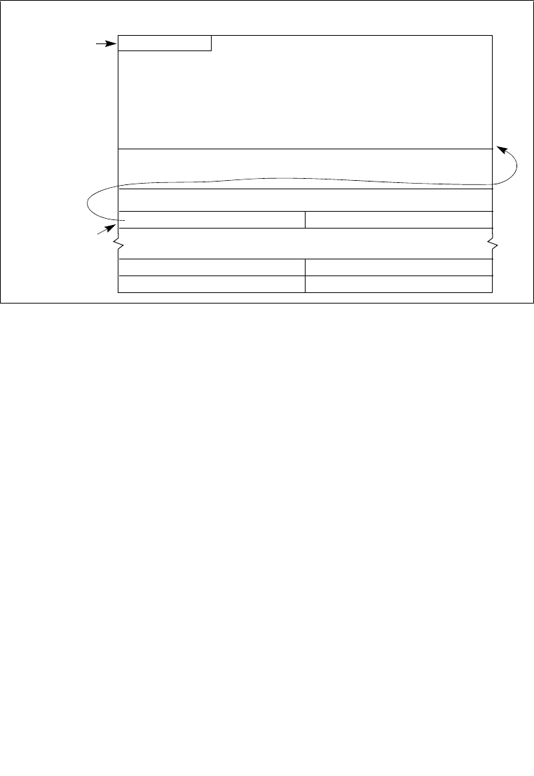
Vol. 3A 15-25
8086 EMULATION
Redirecting software interrupts back to the 8086 program potentially speeds up interrupt
handling because a switch back and forth between virtual-8086 mode and protected mode is not
required. This latter interrupt-handling technique is particularly useful for 8086 operating
systems (such as MS-DOS) that use the INT n instruction to call operating system procedures.
The CPUID instruction can be used to verify that the virtual mode extension is implemented on
the processor. Bit 1 of the feature flags register (EDX) indicates the availability of the virtual
mode extension (see “CPUID—CPU Identification” in Chapter 3, “Instruction Set Reference,
A-M”, of the IA-32 Intel® Architecture Software Developer’s Manual, Volume 2A).
The following sections describe the six methods (or mechanisms) for handling software inter-
rupts in virtual-8086 mode. See Section 15.3.2, “Class 2—Maskable Hardware Interrupt
Handling in Virtual-8086 Mode Using the Virtual Interrupt Mechanism”, for a description of the
use of the VIF and VIP flags in the EFLAGS register for handling maskable hardware interrupts.
15.3.3.1 Method 1: Software Interrupt Handling
When the VME flag in control register CR4 is clear and the IOPL field is 3, a Pentium or later
IA-32 processor handles software interrupts in the same manner as they are handled by an
Intel386 or Intel486 processor. It executes an implicit call to the interrupt handler in the
protected-mode IDT pointed to by the interrupt vector. See Section 15.3.1, “Class 1—Hardware
Interrupt and Exception Handling in Virtual-8086 Mode”, for a complete description of this
mechanism and its possible uses.
Figure 15-5. Software Interrupt Redirection Bit Map in TSS
I/O Map Base
Task-State Segment (TSS)
64H
31 24 23 0
11111111
I/O Permission Bit Map
0
I/O map base
must not exceed
DFFFH.
Last byte of bit
map must be
followed by a
byte with all bits
Software Interrupt Redirection Bit Map (32 Bytes)

15-26 Vol. 3A
8086 EMULATION
15.3.3.2 Methods 2 and 3: Software Interrupt Handling
When a software interrupt occurs in virtual-8086 mode and the method 2 or 3 conditions are
present, the processor generates a general-protection exception (#GP). Method 2 is enabled
when the VME flag is set to 0 and the IOPL value is less than 3. Here the IOPL value is used to
bypass the protected-mode interrupt handlers and cause any software interrupt that occurs in
virtual-8086 mode to be treated as a protected-mode general-protection exception (#GP). The
general-protection exception handler calls the virtual-8086 monitor, which can then emulate an
8086-program interrupt handler or pass control back to the 8086 program’s handler, as described
in Section 15.3.1.2, “Handling an Interrupt or Exception With an 8086 Program Interrupt or
Exception Handler”.
Method 3 is enabled when the VME flag is set to 1, the IOPL value is less than 3, and the corre-
sponding bit for the software interrupt in the software interrupt redirection bit map is set to 1.
Here, the processor performs the same operation as it does for method 2 software interrupt
handling. If the corresponding bit for the software interrupt in the software interrupt redirection
bit map is set to 0, the interrupt is handled using method 6 (see Section 15.3.3.5, “Method 6:
Software Interrupt Handling”).
15.3.3.3 Method 4: Software Interrupt Handling
Method 4 handling is enabled when the VME flag is set to 1, the IOPL value is 3, and the bit for
the interrupt vector in the redirection bit map is set to 1. Method 4 software interrupt handling
allows method 1 style handling when the virtual mode extension is enabled; that is, the interrupt
is directed to a protected-mode handler (see Section 15.3.3.1, “Method 1: Software Interrupt
Handling”).
15.3.3.4 Method 5: Software Interrupt Handling
Method 5 software interrupt handling provides a streamlined method of redirecting software
interrupts (invoked with the INT n instruction) that occur in virtual 8086 mode back to the 8086
program’s interrupt vector table and its interrupt handlers. Method 5 handling is enabled when
the VME flag is set to 1, the IOPL value is 3, and the bit for the interrupt vector in the redirection
bit map is set to 0. The processor performs the following actions to make an implicit call to the
selected 8086 program interrupt handler:
1. Pushes the low-order 16 bits of the EFLAGS register onto the stack.
2. Pushes the current values of the CS and EIP registers onto the current stack. (Only the 16
least-significant bits of the EIP register are pushed and no stack switch occurs.)
3. Clears the IF flag in the EFLAGS register to disable interrupts.
4. Clears the TF flag, in the EFLAGS register.
5. Locates the 8086 program interrupt vector table at linear address 0 for the 8086-mode task.

Vol. 3A 15-27
8086 EMULATION
6. Loads the CS and EIP registers with values from the interrupt vector table entry pointed to
by the interrupt vector number. Only the 16 low-order bits of the EIP are loaded and the 16
high-order bits are set to 0. The interrupt vector table is assumed to be at linear address 0 of
the current virtual-8086 task.
7. Begins executing the selected interrupt handler.
An IRET instruction at the end of the handler procedure reverses these steps to return program
control to the interrupted 8086 program.
Note that with method 5 handling, a mode switch from virtual-8086 mode to protected mode
does not occur. The processor remains in virtual-8086 mode throughout the interrupt-handling
operation.
The method 5 handling actions are virtually identical to the actions the processor takes when
handling software interrupts in real-address mode. The benefit of using method 5 handling to
access the 8086 program handlers is that it avoids the overhead of methods 2 and 3 handling,
which requires first going to the virtual-8086 monitor, then to the 8086 program handler, then
back again to the virtual-8086 monitor, before returning to the interrupted 8086 program (see
Section 15.3.1.2, “Handling an Interrupt or Exception With an 8086 Program Interrupt or
Exception Handler”).
NOTE
Methods 1 and 4 handling can handle a software interrupt in a virtual-8086
task with a regular protected-mode handler, but this approach requires all
virtual-8086 tasks to use the same software interrupt handlers, which
generally does not give sufficient latitude to the programs running in the
virtual-8086 tasks, particularly MS-DOS programs.
15.3.3.5 Method 6: Software Interrupt Handling
Method 6 handling is enabled when the VME flag is set to 1, the IOPL value is less than 3, and
the bit for the interrupt or exception vector in the redirection bit map is set to 0. With method 6
interrupt handling, software interrupts are handled in the same manner as was described for
method 5 handling (see Section 15.3.3.4, “Method 5: Software Interrupt Handling”).
Method 6 differs from method 5 in that with the IOPL value set to less than 3, the VIF and VIP
flags in the EFLAGS register are enabled, providing virtual interrupt support for handling
class 2 maskable hardware interrupts (see Section 15.3.2, “Class 2—Maskable Hardware Inter-
rupt Handling in Virtual-8086 Mode Using the Virtual Interrupt Mechanism”). These flags
provide the virtual-8086 monitor with an efficient means of handling maskable hardware inter-
rupts that occur during a virtual-8086 mode task. Also, because the IOPL value is less than 3
and the VIF flag is enabled, the information pushed on the stack by the processor when invoking
the interrupt handler is slightly different between methods 5 and 6 (see Table 15-2).

15-28 Vol. 3A
8086 EMULATION
15.4 PROTECTED-MODE VIRTUAL INTERRUPTS
The IA-32 processors (beginning with the Pentium processor) also support the VIF and VIP
flags in the EFLAGS register in protected mode by setting the PVI (protected-mode virtual
interrupt) flag in the CR4 register. Setting the PVI flag allows applications running at privilege
level 3 to execute the CLI and STI instructions without causing a general-protection exception
(#GP) or affecting hardware interrupts.
When the PVI flag is set to 1, the CPL is 3, and the IOPL is less than 3, the STI and CLI instruc-
tions set and clear the VIF flag in the EFLAGS register, leaving IF unaffected. In this mode of
operation, an application running in protected mode and at a CPL of 3 can inhibit interrupts in
the same manner as is described in Section 15.3.2, “Class 2—Maskable Hardware Interrupt
Handling in Virtual-8086 Mode Using the Virtual Interrupt Mechanism”, for a virtual-8086
mode task. When the application executes the CLI instruction, the processor clears the VIF flag.
If the processor receives a maskable hardware interrupt, the processor invokes the protected-
mode interrupt handler. This handler checks the state of the VIF flag in the EFLAGS register. If
the VIF flag is clear (indicating that the active task does not want to have interrupts handled
now), the handler sets the VIP flag in the EFLAGS image on the stack and returns to the privi-
lege-level 3 application, which continues program execution. When the application executes a
STI instruction to set the VIF flag, the processor automatically invokes the general-protection
exception handler, which can then handle the pending interrupt. After handing the pending inter-
rupt, the handler typically sets the VIF flag and clears the VIP flag in the EFLAGS image on the
stack and executes a return to the application program. The next time the processor receives a
maskable hardware interrupt, the processor will handle it in the normal manner for interrupts
received while the processor is operating at a CPL of 3.
As with the virtual mode extension (enabled with the VME flag in the CR4 register), the
protected-mode virtual interrupt extension only affects maskable hardware interrupts (interrupt
vectors 32 through 255). NMI interrupts and exceptions are handled in the normal manner.
When protected-mode virtual interrupts are disabled (that is, when the PVI flag in control
register CR4 is set to 0, the CPL is less than 3, or the IOPL value is 3), then the CLI and STI
instructions execute in a manner compatible with the Intel486 processor. That is, if the CPL is
greater (less privileged) than the I/O privilege level (IOPL), a general-protection exception
occurs. If the IOPL value is 3, CLI and STI clear or set the IF flag, respectively.
PUSHF, POPF, IRET and INT are executed like in the Intel486 processor, regardless of whether
protected-mode virtual interrupts are enabled.
It is only possible to enter virtual-8086 mode through a task switch or the execution of an IRET
instruction, and it is only possible to leave virtual-8086 mode by faulting to a protected-mode
interrupt handler (typically the general-protection exception handler, which in turn calls the
virtual 8086-mode monitor). In both cases, the EFLAGS register is saved and restored. This is
not true, however, in protected mode when the PVI flag is set and the processor is not in virtual-
8086 mode. Here, it is possible to call a procedure at a different privilege level, in which case
the EFLAGS register is not saved or modified. However, the states of VIF and VIP flags are
never examined by the processor when the CPL is not 3.

16
Mixing 16-Bit
and 32-Bit Code

Vol. 3A 16-1
CHAPTER 16
MIXING 16-BIT AND 32-BIT CODE
Program modules written to run on IA-32 processors can be either 16-bit modules or 32-bit
modules. Table 16-1 shows the characteristic of 16-bit and 32-bit modules.
The IA-32 processors function most efficiently when executing 32-bit program modules. They
can, however, also execute 16-bit program modules, in any of the following ways:
•In real-address mode.
•In virtual-8086 mode.
•System management mode (SMM).
•As a protected-mode task, when the code, data, and stack segments for the task are all
configured as a 16-bit segments.
•By integrating 16-bit and 32-bit segments into a single protected-mode task.
•By integrating 16-bit operations into 32-bit code segments.
Real-address mode, virtual-8086 mode, and SMM are native 16-bit modes. A legacy program
assembled and/or compiled to run on an Intel 8086 or Intel 286 processor should run in real-
address mode or virtual-8086 mode without modification. Sixteen-bit program modules can also
be written to run in real-address mode for handling system initialization or to run in SMM for
handling system management functions. See Chapter 15, “8086 Emulation,” for detailed infor-
mation on real-address mode and virtual-8086 mode; see Chapter 24, “System Management,”
for information on SMM.
This chapter describes how to integrate 16-bit program modules with 32-bit program modules
when operating in protected mode and how to mix 16-bit and 32-bit code within 32-bit code
segments.
Table 16-1. Characteristics of 16-Bit and 32-Bit Program Modules
Characteristic 16-Bit Program Modules 32-Bit Program Modules
Segment Size 0 to 64 KBytes 0 to 4 GBytes
Operand Sizes 8 bits and 16 bits 8 bits and 32 bits
Pointer Offset Size (Address Size) 16 bits 32 bits
Stack Pointer Size 16 Bits 32 Bits
Control Transfers Allowed to Code
Segments of This Size 16 Bits 32 Bits

16-2 Vol. 3A
MIXING 16-BIT AND 32-BIT CODE
16.1 DEFINING 16-BIT AND 32-BIT PROGRAM MODULES
The following IA-32 architecture mechanisms are used to distinguish between and support
16-bit and 32-bit segments and operations:
•The D (default operand and address size) flag in code-segment descriptors.
•The B (default stack size) flag in stack-segment descriptors.
•16-bit and 32-bit call gates, interrupt gates, and trap gates.
•Operand-size and address-size instruction prefixes.
•16-bit and 32-bit general-purpose registers.
The D flag in a code-segment descriptor determines the default operand-size and address-size
for the instructions of a code segment. (In real-address mode and virtual-8086 mode, which do
not use segment descriptors, the default is 16 bits.) A code segment with its D flag set is a 32-bit
segment; a code segment with its D flag clear is a 16-bit segment.
The B flag in the stack-segment descriptor specifies the size of stack pointer (the 32-bit ESP
register or the 16-bit SP register) used by the processor for implicit stack references. The B flag
for all data descriptors also controls upper address range for expand down segments.
When transferring program control to another code segment through a call gate, interrupt gate,
or trap gate, the operand size used during the transfer is determined by the type of gate used
(16-bit or 32-bit), (not by the D-flag or prefix of the transfer instruction). The gate type deter-
mines how return information is saved on the stack (or stacks).
For most efficient and trouble-free operation of the processor, 32-bit programs or tasks should
have the D flag in the code-segment descriptor and the B flag in the stack-segment descriptor
set, and 16-bit programs or tasks should have these flags clear. Program control transfers from
16-bit segments to 32-bit segments (and vice versa) are handled most efficiently through call,
interrupt, or trap gates.
Instruction prefixes can be used to override the default operand size and address size of a code
segment. These prefixes can be used in real-address mode as well as in protected mode and
virtual-8086 mode. An operand-size or address-size prefix only changes the size for the duration
of the instruction.
16.2 MIXING 16-BIT AND 32-BIT OPERATIONS WITHIN A CODE
SEGMENT
The following two instruction prefixes allow mixing of 32-bit and 16-bit operations within one
segment:
•The operand-size prefix (66H)
•The address-size prefix (67H)

Vol. 3A 16-3
MIXING 16-BIT AND 32-BIT CODE
These prefixes reverse the default size selected by the D flag in the code-segment descriptor. For
example, the processor can interpret the (MOV mem, reg) instruction in any of four ways:
•In a 32-bit code segment:
— Moves 32 bits from a 32-bit register to memory using a 32-bit effective address.
— If preceded by an operand-size prefix, moves 16 bits from a 16-bit register to memory
using a 32-bit effective address.
— If preceded by an address-size prefix, moves 32 bits from a 32-bit register to memory
using a 16-bit effective address.
— If preceded by both an address-size prefix and an operand-size prefix, moves 16 bits
from a 16-bit register to memory using a 16-bit effective address.
•In a 16-bit code segment:
— Moves 16 bits from a 16-bit register to memory using a 16-bit effective address.
— If preceded by an operand-size prefix, moves 32 bits from a 32-bit register to memory
using a 16-bit effective address.
— If preceded by an address-size prefix, moves 16 bits from a 16-bit register to memory
using a 32-bit effective address.
— If preceded by both an address-size prefix and an operand-size prefix, moves 32 bits
from a 32-bit register to memory using a 32-bit effective address.
The previous examples show that any instruction can generate any combination of operand size
and address size regardless of whether the instruction is in a 16- or 32-bit segment. The choice
of the 16- or 32-bit default for a code segment is normally based on the following criteria:
•Performance — Always use 32-bit code segments when possible. They run much faster
than 16-bit code segments on P6 family processors, and somewhat faster on earlier IA-32
processors.
•The operating system the code segment will be running on — If the operating system is
a 16-bit operating system, it may not support 32-bit program modules.
•Mode of operation — If the code segment is being designed to run in real-address mode,
virtual-8086 mode, or SMM, it must be a 16-bit code segment.
•Backward compatibility to earlier IA-32 processors — If a code segment must be able
to run on an Intel 8086 or Intel 286 processor, it must be a 16-bit code segment.
16.3 SHARING DATA AMONG MIXED-SIZE CODE SEGMENTS
Data segments can be accessed from both 16-bit and 32-bit code segments. When a data segment
that is larger than 64 KBytes is to be shared among 16- and 32-bit code segments, the data that
is to be accessed from the 16-bit code segments must be located within the first 64 KBytes of
the data segment. The reason for this is that 16-bit pointers by definition can only point to the
first 64 KBytes of a segment.

16-4 Vol. 3A
MIXING 16-BIT AND 32-BIT CODE
A stack that spans less than 64 KBytes can be shared by both 16- and 32-bit code segments. This
class of stacks includes:
•Stacks in expand-up segments with the G (granularity) and B (big) flags in the stack-
segment descriptor clear.
•Stacks in expand-down segments with the G and B flags clear.
•Stacks in expand-up segments with the G flag set and the B flag clear and where the stack
is contained completely within the lower 64 KBytes. (Offsets greater than FFFFH can be
used for data, other than the stack, which is not shared.)
See Section 3.4.5, “Segment Descriptors,” for a description of the G and B flags and the expand-
down stack type.
The B flag cannot, in general, be used to change the size of stack used by a 16-bit code segment.
This flag controls the size of the stack pointer only for implicit stack references such as those
caused by interrupts, exceptions, and the PUSH, POP, CALL, and RET instructions. It does not
control explicit stack references, such as accesses to parameters or local variables. A 16-bit code
segment can use a 32-bit stack only if the code is modified so that all explicit references to the
stack are preceded by the 32-bit address-size prefix, causing those references to use 32-bit
addressing and explicit writes to the stack pointer are preceded by a 32-bit operand-size prefix.
In 32-bit, expand-down segments, all offsets may be greater than 64 KBytes; therefore, 16-bit
code cannot use this kind of stack segment unless the code segment is modified to use 32-bit
addressing.
16.4 TRANSFERRING CONTROL AMONG MIXED-SIZE CODE
SEGMENTS
There are three ways for a procedure in a 16-bit code segment to safely make a call to a 32-bit
code segment:
•Make the call through a 32-bit call gate.
•Make a 16-bit call to a 32-bit interface procedure. The interface procedure then makes a
32-bit call to the intended destination.
•Modify the 16-bit procedure, inserting an operand-size prefix before the call, to change it
to a 32-bit call.
Likewise, there are three ways for procedure in a 32-bit code segment to safely make a call to a
16-bit code segment:
•Make the call through a 16-bit call gate. Here, the EIP value at the CALL instruction
cannot exceed FFFFH.
•Make a 32-bit call to a 16-bit interface procedure. The interface procedure then makes a
16-bit call to the intended destination.
•Modify the 32-bit procedure, inserting an operand-size prefix before the call, changing it to
a 16-bit call. Be certain that the return offset does not exceed FFFFH.

Vol. 3A 16-5
MIXING 16-BIT AND 32-BIT CODE
These methods of transferring program control overcome the following architectural limitations
imposed on calls between 16-bit and 32-bit code segments:
•Pointers from 16-bit code segments (which by default can only be 16 bits) cannot be used
to address data or code located beyond FFFFH in a 32-bit segment.
•The operand-size attributes for a CALL and its companion RETURN instruction must be
the same to maintain stack coherency. This is also true for implicit calls to interrupt and
exception handlers and their companion IRET instructions.
•A 32-bit parameters (particularly a pointer parameter) greater than FFFFH cannot be
squeezed into a 16-bit parameter location on a stack.
•The size of the stack pointer (SP or ESP) changes when switching between 16-bit and
32-bit code segments.
These limitations are discussed in greater detail in the following sections.
16.4.1 Code-Segment Pointer Size
For control-transfer instructions that use a pointer to identify the next instruction (that is, those
that do not use gates), the operand-size attribute determines the size of the offset portion of the
pointer. The implications of this rule are as follows:
•A JMP, CALL, or RET instruction from a 32-bit segment to a 16-bit segment is always
possible using a 32-bit operand size, providing the 32-bit pointer does not exceed FFFFH.
•A JMP, CALL, or RET instruction from a 16-bit segment to a 32-bit segment cannot
address a destination greater than FFFFH, unless the instruction is given an operand-size
prefix.
See Section 16.4.5, “Writing Interface Procedures,” for an interface procedure that can transfer
program control from 16-bit segments to destinations in 32-bit segments beyond FFFFH.
16.4.2 Stack Management for Control Transfer
Because the stack is managed differently for 16-bit procedure calls than for 32-bit calls, the
operand-size attribute of the RET instruction must match that of the CALL instruction (see
Figure 16-1). On a 16-bit call, the processor pushes the contents of the 16-bit IP register and (for
calls between privilege levels) the 16-bit SP register. The matching RET instruction must also
use a 16-bit operand size to pop these 16-bit values from the stack into the 16-bit registers.
A 32-bit CALL instruction pushes the contents of the 32-bit EIP register and (for inter-privilege-
level calls) the 32-bit ESP register. Here, the matching RET instruction must use a 32-bit
operand size to pop these 32-bit values from the stack into the 32-bit registers. If the two parts
of a CALL/RET instruction pair do not have matching operand sizes, the stack will not be
managed correctly and the values of the instruction pointer and stack pointer will not be restored
to correct values.
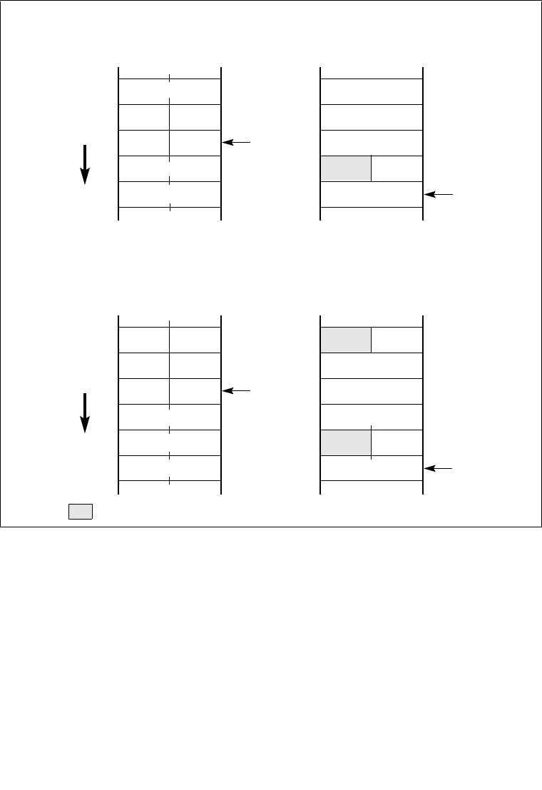
16-6 Vol. 3A
MIXING 16-BIT AND 32-BIT CODE
While executing 32-bit code, if a call is made to a 16-bit code segment which is at the same or
a more privileged level (that is, the DPL of the called code segment is less than or equal to the
CPL of the calling code segment) through a 16-bit call gate, then the upper 16-bits of the ESP
register may be unreliable upon returning to the 32-bit code segment (that is, after executing a
RET in the 16-bit code segment).
When the CALL instruction and its matching RET instruction are in code segments that have D
flags with the same values (that is, both are 32-bit code segments or both are 16-bit code
segments), the default settings may be used. When the CALL instruction and its matching RET
instruction are in segments which have different D-flag settings, an operand-size prefix must be
used.
Figure 16-1. Stack after Far 16- and 32-Bit Calls
SP
After 16-bit Call
PARM 1
IP SP
SS
PARM 2
CS
031
SS
EIP
After 32-bit Call
CS
ESP
ESP
PARM 2
PARM 1
031
With Privilege Transition
Stack
Growth
After 16-bit Call
PARM 1
IP SP
PARM 2
CS
031
Without Privilege Transition
Stack
Growth
After 32-bit Call
PARM 1
ESP
PARM 2
CS
031
EIP
Undefined

Vol. 3A 16-7
MIXING 16-BIT AND 32-BIT CODE
16.4.2.1 Controlling the Operand-Size Attribute For a Call
Three things can determine the operand-size of a call:
•The D flag in the segment descriptor for the calling code segment.
•An operand-size instruction prefix.
•The type of call gate (16-bit or 32-bit), if a call is made through a call gate.
When a call is made with a pointer (rather than a call gate), the D flag for the calling code
segment determines the operand-size for the CALL instruction. This operand-size attribute can
be overridden by prepending an operand-size prefix to the CALL instruction. So, for example,
if the D flag for a code segment is set for 16 bits and the operand-size prefix is used with a
CALL instruction, the processor will cause the information stored on the stack to be stored in
32-bit format. If the call is to a 32-bit code segment, the instructions in that code segment will
be able to read the stack coherently. Also, a RET instruction from the 32-bit code segment
without an operand-size prefix will maintain stack coherency with the 16-bit code segment
being returned to.
When a CALL instruction references a call-gate descriptor, the type of call is determined by the
type of call gate (16-bit or 32-bit). The offset to the destination in the code segment being called
is taken from the gate descriptor; therefore, if a 32-bit call gate is used, a procedure in a 16-bit
code segment can call a procedure located more than 64 KBytes from the base of a 32-bit code
segment, because a 32-bit call gate uses a 32-bit offset.
Note that regardless of the operand size of the call and how it is determined, the size of the stack
pointer used (SP or ESP) is always controlled by the B flag in the stack-segment descriptor
currently in use (that is, when B is clear, SP is used, and when B is set, ESP is used).
An unmodified 16-bit code segment that has run successfully on an 8086 processor or in
real-mode on a later IA-32 architecture processor will have its D flag clear and will not use
operand-size override prefixes. As a result, all CALL instructions in this code segment will use
the 16-bit operand-size attribute. Procedures in these code segments can be modified to safely
call procedures to 32-bit code segments in either of two ways:
•Relink the CALL instruction to point to 32-bit call gates (see Section 16.4.2.2, “Passing
Parameters With a Gate”).
•Add a 32-bit operand-size prefix to each CALL instruction.
16.4.2.2 Passing Parameters With a Gate
When referencing 32-bit gates with 16-bit procedures, it is important to consider the number of
parameters passed in each procedure call. The count field of the gate descriptor specifies the size
of the parameter string to copy from the current stack to the stack of a more privileged (numer-
ically lower privilege level) procedure. The count field of a 16-bit gate specifies the number of
16-bit words to be copied, whereas the count field of a 32-bit gate specifies the number of 32-bit
doublewords to be copied. The count field for a 32-bit gate must thus be half the size of the
number of words being placed on the stack by a 16-bit procedure. Also, the 16-bit procedure
must use an even number of words as parameters.

16-8 Vol. 3A
MIXING 16-BIT AND 32-BIT CODE
16.4.3 Interrupt Control Transfers
A program-control transfer caused by an exception or interrupt is always carried out through an
interrupt or trap gate (located in the IDT). Here, the type of the gate (16-bit or 32-bit) determines
the operand-size attribute used in the implicit call to the exception or interrupt handler procedure
in another code segment.
A 32-bit interrupt or trap gate provides a safe interface to a 32-bit exception or interrupt handler
when the exception or interrupt occurs in either a 32-bit or a 16-bit code segment. It is sometimes
impractical, however, to place exception or interrupt handlers in 16-bit code segments, because
only 16-bit return addresses are saved on the stack. If an exception or interrupt occurs in a 32-bit
code segment when the EIP was greater than FFFFH, the 16-bit handler procedure cannot
provide the correct return address.
16.4.4 Parameter Translation
When segment offsets or pointers (which contain segment offsets) are passed as parameters
between 16-bit and 32-bit procedures, some translation is required. If a 32-bit procedure passes
a pointer to data located beyond 64 KBytes to a 16-bit procedure, the 16-bit procedure cannot
use it. Except for this limitation, interface code can perform any format conversion between
32-bit and 16-bit pointers that may be needed.
Parameters passed by value between 32-bit and 16-bit code also may require translation between
32-bit and 16-bit formats. The form of the translation is application-dependent.
16.4.5 Writing Interface Procedures
Placing interface code between 32-bit and 16-bit procedures can be the solution to the following
interface problems:
•Allowing procedures in 16-bit code segments to call procedures with offsets greater than
FFFFH in 32-bit code segments.
•Matching operand-size attributes between companion CALL and RET instructions.
•Translating parameters (data), including managing parameter strings with a variable count
or an odd number of 16-bit words.
•The possible invalidation of the upper bits of the ESP register.
The interface procedure is simplified where these rules are followed.
1. The interface procedure must reside in a 32-bit code segment (the D flag for the code-
segment descriptor is set).
2. All procedures that may be called by 16-bit procedures must have offsets not greater than
FFFFH.
3. All return addresses saved by 16-bit procedures must have offsets not greater than FFFFH.

Vol. 3A 16-9
MIXING 16-BIT AND 32-BIT CODE
The interface procedure becomes more complex if any of these rules are violated. For example,
if a 16-bit procedure calls a 32-bit procedure with an entry point beyond FFFFH, the interface
procedure will need to provide the offset to the entry point. The mapping between 16- and 32-bit
addresses is only performed automatically when a call gate is used, because the gate descriptor
for a call gate contains a 32-bit address. When a call gate is not used, the interface code must
provide the 32-bit address.
The structure of the interface procedure depends on the types of calls it is going to support, as
follows:
•Calls from 16-bit procedures to 32-bit procedures — Calls to the interface procedure
from a 16-bit code segment are made with 16-bit CALL instructions (by default, because
the D flag for the calling code-segment descriptor is clear), and 16-bit operand-size
prefixes are used with RET instructions to return from the interface procedure to the
calling procedure. Calls from the interface procedure to 32-bit procedures are performed
with 32-bit CALL instructions (by default, because the D flag for the interface procedure’s
code segment is set), and returns from the called procedures to the interface procedure are
performed with 32-bit RET instructions (also by default).
•Calls from 32-bit procedures to 16-bit procedures — Calls to the interface procedure
from a 32-bit code segment are made with 32-bit CALL instructions (by default), and
returns to the calling procedure from the interface procedure are made with 32-bit RET
instructions (also by default). Calls from the interface procedure to 16-bit procedures
require the CALL instructions to have the operand-size prefixes, and returns from the
called procedures to the interface procedure are performed with 16-bit RET instructions
(by default).

16-10 Vol. 3A
MIXING 16-BIT AND 32-BIT CODE

17
IA-32 Architecture
Compatibility

Vol. 3A 17-1
CHAPTER 17
IA-32 ARCHITECTURE COMPATIBILITY
All IA-32 processors are binary compatible. Compatibility means that, within certain limited
constraints, programs that execute on previous generations of IA-32 processors will produce
identical results when executed on later IA-32 processors. The compatibility constraints and any
implementation differences between the IA-32 processors are described in this chapter.
Each new IA-32 processor has enhanced the software visible architecture from that found in
earlier IA-32 processors. Those enhancements have been defined with consideration for
compatibility with previous and future processors. This chapter also summarizes the compati-
bility considerations for those extensions.
17.1. IA-32 PROCESSOR FAMILIES AND CATEGORIES
IA-32 processors are referred to in several different ways in this chapter, depending on the type
of compatibility information being related, as described in the following:
•IA-32 Processors — All the Intel processors based on the Intel IA-32 Architecture, which
include the 8086/88, Intel 286, Intel386, Intel486, Pentium, Pentium Pro, Pentium II,
Pentium III, Pentium 4, and Intel Xeon processors.
•32-bit Processors — All the IA-32 processors that use a 32-bit architecture, which include
the Intel386, Intel486, Pentium, Pentium Pro, Pentium II, Pentium III, Pentium 4, and Intel
Xeon processors.
•16-bit Processors — All the IA-32 processors that use a 16-bit architecture, which include
the 8086/88 and Intel 286 processors.
•P6 Family Processors — All the IA-32 processors that are based on the P6 microarchi-
tecture, which include the Pentium Pro, Pentium II, and Pentium III processors.
•Pentium 4 Family Processors — A family of IA-32 processors that is based on the Intel
NetBurst microarchitecture.
•Intel Xeon Family Processors — A family of IA-32 processors that is based on the Intel
NetBurst microarchitecture. This family includes the Intel Xeon processor and the Intel
Xeon processor MP.
•Pentium D Processors — A family of dual-core IA-32 processors that provides two
processor cores in a physical package. Each core is based on the Intel NetBurst microar-
chitecture.
•Pentium Processor Extreme Editions — A family of dual-core IA-32 processors that
provides two processor cores in a physical package. Each core is based on the Intel
NetBurst microarchitecture and supports Hyper-Threading Technology.

17-2 Vol. 3A
IA-32 ARCHITECTURE COMPATIBILITY
17.2. RESERVED BITS
Throughout this manual, certain bits are marked as reserved in many register and memory layout
descriptions. When bits are marked as undefined or reserved, it is essential for compatibility
with future processors that software treat these bits as having a future, though unknown effect.
Software should follow these guidelines in dealing with reserved bits:
•Do not depend on the states of any reserved bits when testing the values of registers or
memory locations that contain such bits. Mask out the reserved bits before testing.
•Do not depend on the states of any reserved bits when storing them to memory or to a
register.
•Do not depend on the ability to retain information written into any reserved bits.
•When loading a register, always load the reserved bits with the values indicated in the
documentation, if any, or reload them with values previously read from the same register.
Software written for existing IA-32 processor that handles reserved bits correctly will port to
future IA-32 processors without generating protection exceptions.
17.3. ENABLING NEW FUNCTIONS AND MODES
Most of the new control functions defined for the P6 family and Pentium processors are enabled
by new mode flags in the control registers (primarily register CR4). This register is undefined
for IA-32 processors earlier than the Pentium processor. Attempting to access this register with
an Intel486 or earlier IA-32 processor results in an invalid-opcode exception (#UD). Conse-
quently, programs that execute correctly on the Intel486 or earlier IA-32 processor cannot erro-
neously enable these functions. Attempting to set a reserved bit in register CR4 to a value other
than its original value results in a general-protection exception (#GP). So, programs that execute
on the P6 family and Pentium processors cannot erroneously enable functions that may be
implemented in future IA-32 processors.
The P6 family and Pentium processors do not check for attempts to set reserved bits in model-
specific registers. It is the obligation of the software writer to enforce this discipline. These
reserved bits may be used in future Intel processors.
17.4. DETECTING THE PRESENCE OF NEW FEATURES
THROUGH SOFTWARE
Software can check for the presence of new architectural features and extensions in either of two
ways:
1. Test for the presence of the feature or extension. Software can test for the presence of new
flags in the EFLAGS register and control registers. If these flags are reserved (meaning not
present in the processor executing the test), an exception is generated. Likewise, software
can attempt to execute a new instruction, which results in an invalid-opcode exception
(#UD) being generated if it is not supported.

Vol. 3A 17-3
IA-32 ARCHITECTURE COMPATIBILITY
2. Execute the CPUID instruction. The CPUID instruction (added to the IA-32 in the Pentium
processor) indicates the presence of new features directly.
See Chapter 14, “Processor Identification and Feature Determination,” in the IA-32 Intel®
Architecture Software Developer’s Manual, Volume 1, for detailed information on detecting new
processor features and extensions.
17.5. INTEL MMX TECHNOLOGY
The Pentium processor with MMX technology introduced the MMX technology and a set of
MMX instructions to the IA-32. The MMX instructions are described in Chapter 9, “Program-
ming with Intel® MMX™ Technology,” in the IA-32 Intel® Architecture Software Developer’s
Manual, Volume 1, and in the IA-32 Intel® Architecture Software Developer’s Manual, Volumes
2A & 2B. The MMX technology and MMX instructions are also included in the Pentium II,
Pentium III, Pentium 4, and Intel Xeon processors.
17.6. STREAMING SIMD EXTENSIONS (SSE)
The Streaming SIMD Extensions (SSE) were introduced in the Pentium III processor. The SSE
extensions consist of a new set of instructions and a new set of registers. The new register
include the eight 128-bit XXM registers and the 32-bit MXCSR control and status register.
These instructions and registers are designed to allow SIMD computations to be made on single-
precision floating-point numbers. Several of these new instructions also operate in the MMX
registers. SSE instructions and registers are described in Section 10, “Programming with
Streaming SIMD Extensions (SSE),” in the IA-32 Intel® Architecture Software Developer’s
Manual, Volume 1, and in the IA-32 Intel® Architecture Software Developer’s Manual, Volumes
2A & 2B.
17.7. STREAMING SIMD EXTENSIONS 2 (SSE2)
The Streaming SIMD Extensions 2 (SSE2) were introduced in the Pentium 4 and Intel Xeon
processors. They consist of a new set of instructions that operate on the XXM and MXCSR
registers and perform SIMD operations on double-precision floating-point values and on integer
values. Several of these new instructions also operate in the MMX registers. SSE2 instructions
and registers are described in Chapter 11, “Programming with Streaming SIMD Extensions 2
(SSE3),” in the IA-32 Intel® Architecture Software Developer’s Manual, Volume 1, and in the
IA-32 Intel® Architecture Software Developer’s Manual, Volumes 2A & 2B.
17.8. STREAMING SIMD EXTENSIONS 3 (SSE3)
The Streaming SIMD Extensions 3 (SSE3) were introduced in Pentium 4 processors supporting
Hyper-Threading Technology and Intel Xeon processors. SSE3 extensions include 13 instruc-
tions. Ten of these 13 instructions support the single instruction multiple data (SIMD) execution
model used with SSE/SSE2 extensions. One SSE3 instruction accelerates x87 style program-

17-4 Vol. 3A
IA-32 ARCHITECTURE COMPATIBILITY
ming for conversion to integer. The remaining two instructions (MONITOR and MWAIT)
accelerate synchronization of threads. SSE3 instructions are described in Chapter 12,
“Programming with Streaming SIMD Extensions 3 (SSE3),” in the IA-32 Intel® Architecture
Software Developer’s Manual, Volume 1, and in the IA-32 Intel® Architecture Software Devel-
oper’s Manual, Volumes 2A & 2B.
17.9. HYPER-THREADING TECHNOLOGY
Hyper-Threading Technology is an extension to IA-32 architecture. The feature provides two
logical processors that can execute two separate code streams (called threads) concurrently by
using shared resources in single processor core or in a physical package.
This feature was introduced in the Intel Xeon processor MP and later steppings of the Intel Xeon
processor, and Pentium 4 processors supporting Hyper-Threading Technology. The feature is
also found in the Pentium processor Extreme Edition. See also: Section 7.8, “Intel® Hyper-
Threading Technology Architecture.”
17.10. DUAL-CORE TECHNOLOGY
The Pentium D processor and Pentium processor Extreme Edition provide two processor cores
in each physical processor package. See also: Section 7.6, “Hyper-Threading and Multi-Core
Technology,” and Section 7.9, “Dual-Core Architecture.”
17.11. SPECIFIC FEATURES OF DUAL-CORE PROCESSOR
Dual-core processors may have some processor-specific features. Use CPUID feature flags to
detect the availability features. Note the following:
•CPUID Brand String — On Pentium processor Extreme Edition, the process will report
the correct brand string only after the correct microcode updates are loaded.
•Enhanced Intel SpeedStep Technology — This feature is supported in Pentium D
processor but not in Pentium processor Extreme Edition.
17.12. NEW INSTRUCTIONS IN THE PENTIUM AND LATER IA-32
PROCESSORS
Table 17-1 identifies the instructions introduced into the IA-32 in the Pentium processor and
later IA-32 processors.

Vol. 3A 17-5
IA-32 ARCHITECTURE COMPATIBILITY
17.12.1 Instructions Added Prior to the Pentium Processor
The following instructions were added in the Intel486 processor:
•BSWAP (byte swap) instruction.
•XADD (exchange and add) instruction.
•CMPXCHG (compare and exchange) instruction.
•ΙNVD (invalidate cache) instruction.
•WBINVD (write-back and invalidate cache) instruction.
•INVLPG (invalidate TLB entry) instruction.
The following instructions were added in the Intel386 processor:
•LSS, LFS, and LGS (load SS, FS, and GS registers).
•Long-displacement conditional jumps.
•Single-bit instructions.
Table 17-1. New Instruction in the Pentium Processor and Later IA-32
Processors
Instruction CPUID Identification Bits Introduced In
CMOVcc (conditional move) EDX, Bit 15 Pentium Pro processor
FCMOVcc (floating-point conditional move) EDX, Bits 0 and 15
FCOMI (floating-point compare and set
EFLAGS) EDX, Bits 0 and 15
RDPMC (read performance monitoring
counters) EAX, Bits 8-11, set to 6H;
see Note 1
UD2 (undefined) EAX, Bits 8-11, set to 6H
CMPXCHG8B (compare and exchange 8
bytes) EDX, Bit 8 Pentium processor
CPUID (CPU identification) None; see Note 2
RDTSC (read time-stamp counter) EDX, Bit 4
RDMSR (read model-specific register) EDX, Bit 5
WRMSR (write model-specific register) EDX, Bit 5
MMX Instructions EDX, Bit 23
NOTES:
1. The RDPMC instruction was introduced in the P6 family of processors and added to later model
Pentium processors. This instruction is model specific in nature and not architectural.
2. The CPUID instruction is available in all Pentium and P6 family processors and in later models of the
Intel486 processors. The ability to set and clear the ID flag (bit 21) in the EFLAGS register indicates
the availability of the CPUID instruction.

17-6 Vol. 3A
IA-32 ARCHITECTURE COMPATIBILITY
•Bit scan instructions.
•Double-shift instructions.
•Byte set on condition instruction.
•Move with sign/zero extension.
•Generalized multiply instruction.
•MOV to and from control registers.
•MOV to and from test registers (now obsolete).
•MOV to and from debug registers.
•RSM (resume from SMM). This instruction was introduced in the Intel386 SL and
Intel486 SL processors.
The following instructions were added in the Intel 387 math coprocessor:
•FPREM1.
•FUCOM, FUCOMP, and FUCOMPP.
17.13. OBSOLETE INSTRUCTIONS
The MOV to and from test registers instructions were removed from the Pentium processor and
future IA-32 processors. Execution of these instructions generates an invalid-opcode exception
(#UD).
17.14. UNDEFINED OPCODES
All new instructions defined for IA-32 processors use binary encodings that were reserved on
earlier-generation processors. Attempting to execute a reserved opcode always results in an
invalid-opcode (#UD) exception being generated. Consequently, programs that execute
correctly on earlier-generation processors cannot erroneously execute these instructions and
thereby produce unexpected results when executed on later IA-32 processors.
17.15. NEW FLAGS IN THE EFLAGS REGISTER
The section titled “EFLAGS Register” in Chapter 3, “Basic Execution Environment,” of the
IA-32 Intel® Architecture Software Developer’s Manual, Volume 1, shows the configuration of
flags in the EFLAGS register for the P6 family processors. No new flags have been added to
this register in the P6 family processors. The flags added to this register in the Pentium and
Intel486 processors are described in the following sections.
The following flags were added to the EFLAGS register in the Pentium processor:
•VIF (virtual interrupt flag), bit 19.

Vol. 3A 17-7
IA-32 ARCHITECTURE COMPATIBILITY
•VIP (virtual interrupt pending), bit 20.
•ID (identification flag), bit 21.
The AC flag (bit 18) was added to the EFLAGS register in the Intel486 processor.
17.15.1 Using EFLAGS Flags to Distinguish Between 32-Bit IA-32
Processors
The following bits in the EFLAGS register that can be used to differentiate between the 32-bit
IA-32 processors:
•Bit 18 (the AC flag) can be used to distinguish an Intel386 processor from the P6 family,
Pentium, and Intel486 processors. Since it is not implemented on the Intel386 processor, it
will always be clear.
•Bit 21 (the ID flag) indicates whether an application can execute the CPUID instruction.
The ability to set and clear this bit indicates that the processor is a P6 family or Pentium
processor. The CPUID instruction can then be used to determine which processor.
•Bits 19 (the VIF flag) and 20 (the VIP flag) will always be zero on processors that do not
support virtual mode extensions, which includes all 32-bit processors prior to the Pentium
processor.
See Chapter 14, “Processor Identification and Feature Determination,” in the
IA-32 Intel® Archi-
tecture Software Developer’s Manual, Volume 1,
for more information on identifying processors.
17.16. STACK OPERATIONS
This section identifies the differences in stack implementation between the various IA-32
processors.
17.16.1 PUSH SP
The P6 family, Pentium, Intel486, Intel386, and Intel 286 processors push a different value on
the stack for a PUSH SP instruction than the 8086 processor. The 32-bit processors push the
value of the SP register before it is decremented as part of the push operation; the 8086 processor
pushes the value of the SP register after it is decremented. If the value pushed is important,
replace PUSH SP instructions with the following three instructions:
PUSH BP
MOV BP, SP
XCHG BP, [BP]
This code functions as the 8086 processor PUSH SP instruction on the P6 family, Pentium,
Intel486, Intel386, and Intel 286 processors.

17-8 Vol. 3A
IA-32 ARCHITECTURE COMPATIBILITY
17.16.2 EFLAGS Pushed on the Stack
The setting of the stored values of bits 12 through 15 (which includes the IOPL field and the NT
flag) in the EFLAGS register by the PUSHF instruction, by interrupts, and by exceptions is
different with the 32-bit IA-32 processors than with the 8086 and Intel 286 processors. The
differences are as follows:
•8086 processor—bits 12 through 15 are always set.
•Intel 286 processor—bits 12 through 15 are always cleared in real-address mode.
•32-bit processors in real-address mode—bit 15 (reserved) is always cleared, and bits 12
through 14 have the last value loaded into them.
17.17. X87 FPU
This section addresses the issues that must be faced when porting floating-point software
designed to run on earlier IA-32 processors and math coprocessors to a Pentium 4, Intel Xeon,
P6 family, or Pentium processor with integrated x87 FPU. To software, a Pentium 4, Intel Xeon,
or P6 family processor looks very much like a Pentium processor. Floating-point software which
runs on a Pentium or Intel486 DX processor, or on an Intel486 SX processor/Intel 487 SX math
coprocessor system or an Intel386 processor/Intel 387 math coprocessor system, will run with
at most minor modifications on a Pentium 4, Intel Xeon, or P6 family processor. To port code
directly from an Intel 286 processor/Intel 287 math coprocessor system or an Intel 8086
processor/8087 math coprocessor system to a Pentium 4, Intel Xeon, P6 family, or Pentium
processor, certain additional issues must be addressed.
In the following sections, the term “32-bit x87 FPUs” refers to the P6 family, Pentium, and
Intel486 DX processors, and to the Intel 487 SX and Intel 387 math coprocessors; the term
“16-bit IA-32 math coprocessors” refers to the Intel 287 and 8087 math coprocessors.
17.17.1 Control Register CR0 Flags
The ET, NE, and MP flags in control register CR0 control the interface between the integer unit
of an IA-32 processor and either its internal x87 FPU or an external math coprocessor. The effect
of these flags in the various IA-32 processors are described in the following paragraphs.
The ET (extension type) flag (bit 4 of the CR0 register) is used in the Intel386 processor to indi-
cate whether the math coprocessor in the system is an Intel 287 math coprocessor (flag is clear)
or an Intel 387 DX math coprocessor (flag is set). This bit is hardwired to 1 in the P6 family,
Pentium, and Intel486 processors.
The NE (Numeric Exception) flag (bit 5 of the CR0 register) is used in the P6 family, Pentium,
and Intel486 processors to determine whether unmasked floating-point exceptions are reported
internally through interrupt vector 16 (flag is set) or externally through an external interrupt
(flag is clear). On a hardware reset, the NE flag is initialized to 0, so software using the auto-
matic internal error-reporting mechanism must set this flag to 1. This flag is nonexistent on the
Intel386 processor.

Vol. 3A 17-9
IA-32 ARCHITECTURE COMPATIBILITY
As on the Intel 286 and Intel386 processors, the MP (monitor coprocessor) flag (bit 1 of register
CR0) determines whether the WAIT/FWAIT instructions or waiting-type floating-point instruc-
tions trap when the context of the x87 FPU is different from that of the currently-executing task.
If the MP and TS flag are set, then a WAIT/FWAIT instruction and waiting instructions will
cause a device-not-available exception (interrupt vector 7). The MP flag is used on the Intel 286
and Intel386 processors to support the use of a WAIT/FWAIT instruction to wait on a device
other than a math coprocessor. The device reports its status through the BUSY# pin. Since the
P6 family, Pentium, and Intel486 processors do not have such a pin, the MP flag has no relevant
use and should be set to 1 for normal operation.
17.17.2 x87 FPU Status Word
This section identifies differences to the x87 FPU status word for the different IA-32 processors
and math coprocessors, the reason for the differences, and their impact on software.
17.17.2.1 CONDITION CODE FLAGS (C0 THROUGH C3)
The following information pertains to differences in the use of the condition code flags (C0
through C3) located in bits 8, 9, 10, and 14 of the x87 FPU status word.
After execution of an FINIT instruction or a hardware reset on a 32-bit x87 FPU, the condition
code flags are set to 0. The same operations on a 16-bit IA-32 math coprocessor leave these flags
intact (they contain their prior value). This difference in operation has no impact on software
and provides a consistent state after reset.
Transcendental instruction results in the core range of the P6 family and Pentium processors may
differ from the Intel486 DX processor and Intel 487 SX math coprocessor by 2 to 3 units in the
last place (ulps)—(see “Transcendental Instruction Accuracy” in Chapter 8, “Programming with
the x87 FPU,” of the IA-32 Intel® Architecture Software Developer’s Manual, Volume 1). As a
result, the value saved in the C1 flag may also differ.
After an incomplete FPREM/FPREM1 instruction, the C0, C1, and C3 flags are set to 0 on the
32-bit x87 FPUs. After the same operation on a 16-bit IA-32 math coprocessor, these flags are
left intact.
On the 32-bit x87 FPUs, the C2 flag serves as an incomplete flag for the FTAN instruction. On
the 16-bit IA-32 math coprocessors, the C2 flag is undefined for the FPTAN instruction. This
difference has no impact on software, because Intel 287 or 8087 programs do not check C2 after
an FPTAN instruction. The use of this flag on later processors allows fast checking of operand
range.
17.17.2.2 STACK FAULT FLAG
When unmasked stack overflow or underflow occurs on a 32-bit x87 FPU, the IE flag (bit 0) and
the SF flag (bit 6) of the x87 FPU status word are set to indicate a stack fault and condition code
flag C1 is set or cleared to indicate overflow or underflow, respectively. When unmasked stack
overflow or underflow occurs on a 16-bit IA-32 math coprocessor, only the IE flag is set. Bit 6

17-10 Vol. 3A
IA-32 ARCHITECTURE COMPATIBILITY
is reserved on these processors. The addition of the SF flag on a 32-bit x87 FPU has no impact
on software. Existing exception handlers need not change, but may be upgraded to take advan-
tage of the additional information.
17.17.3 x87 FPU Control Word
Only affine closure is supported for infinity control on a 32-bit x87 FPU. The infinity control
flag (bit 12 of the x87 FPU control word) remains programmable on these processors, but has
no effect. This change was made to conform to the IEEE Standard 754 for Binary Floating-Point
Arithmetic. On a 16-bit IA-32 math coprocessor, both affine and projective closures are
supported, as determined by the setting of bit 12. After a hardware reset, the default value of bit
12 is projective. Software that requires projective infinity arithmetic may give different results.
17.17.4 x87 FPU Tag Word
When loading the tag word of a 32-bit x87 FPU, using an FLDENV, FRSTOR, or FXRSTOR
(Pentium III processor only) instruction, the processor examines the incoming tag and classifies
the location only as empty or non-empty. Thus, tag values of 00, 01, and 10 are interpreted by
the processor to indicate a non-empty location. The tag value of 11 is interpreted by the
processor to indicate an empty location. Subsequent operations on a non-empty register always
examine the value in the register, not the value in its tag. The FSTENV, FSAVE, and FXSAVE
(Pentium III processor only) instructions examine the non-empty registers and put the correct
values in the tags before storing the tag word.
The corresponding tag for a 16-bit IA-32 math coprocessor is checked before each register
access to determine the class of operand in the register; the tag is updated after every change to
a register so that the tag always reflects the most recent status of the register. Software can load
a tag with a value that disagrees with the contents of a register (for example, the register contains
a valid value, but the tag says special). Here, the 16-bit IA-32 math coprocessors honor the tag
and do not examine the register.
Software written to run on a 16-bit IA-32 math coprocessor may not operate correctly on a 16-bit
x87 FPU, if it uses the FLDENV, FRSTOR, or FXRSTOR instructions to change tags to values
(other than to empty) that are different from actual register contents.
The encoding in the tag word for the 32-bit x87 FPUs for unsupported data formats (including
pseudo-zero and unnormal) is special (10B), to comply with IEEE Standard 754. The encoding
in the 16-bit IA-32 math coprocessors for pseudo-zero and unnormal is valid (00B) and the
encoding for other unsupported data formats is special (10B). Code that recognizes the pseudo-
zero or unnormal format as valid must therefore be changed if it is ported to a 32-bit x87 FPU.
17.17.5 Data Types
This section discusses the differences of data types for the various x87 FPUs and math copro-
cessors.

Vol. 3A 17-11
IA-32 ARCHITECTURE COMPATIBILITY
17.17.5.1 NANS
The 32-bit x87 FPUs distinguish between signaling NaNs (SNaNs) and quiet NaNs (QNaNs).
These x87 FPUs only generate QNaNs and normally do not generate an exception upon encoun-
tering a QNaN. An invalid-operation exception (#I) is generated only upon encountering a
SNaN, except for the FCOM, FIST, and FBSTP instructions, which also generates an invalid-
operation exceptions for a QNaNs. This behavior matches IEEE Standard 754.
The 16-bit IA-32 math coprocessors only generate one kind of NaN (the equivalent of a QNaN),
but the raise an invalid-operation exception upon encountering any kind of NaN.
When porting software written to run on a 16-bit IA-32 math coprocessor to a 32-bit x87 FPU,
uninitialized memory locations that contain QNaNs should be changed to SNaNs to cause the
x87 FPU or math coprocessor to fault when uninitialized memory locations are referenced.
17.17.5.2 PSEUDO-ZERO, PSEUDO-NAN, PSEUDO-INFINITY, AND
UNNORMAL FORMATS
The 32-bit x87 FPUs neither generate nor support the pseudo-zero, pseudo-NaN, pseudo-
infinity, and unnormal formats. Whenever they encounter them in an arithmetic operation, they
raise an invalid-operation exception. The 16-bit IA-32 math coprocessors define and support
special handling for these formats. Support for these formats was dropped to conform with IEEE
Standard 754 for Binary Floating-Point Arithmetic.
This change should not impact software ported from 16-bit IA-32 math coprocessors to 32-bit
x87 FPUs. The 32-bit x87 FPUs do not generate these formats, and therefore will not encounter
them unless software explicitly loads them in the data registers. The only affect may be in how
software handles the tags in the tag word (see also: Section 17.17.4, “x87 FPU Tag Word”).
17.17.6 Floating-Point Exceptions
This section identifies the implementation differences in exception handling for floating-point
instructions in the various x87 FPUs and math coprocessors.
17.17.6.1 DENORMAL OPERAND EXCEPTION (#D)
When the denormal operand exception is masked, the 32-bit x87 FPUs automatically normalize
denormalized numbers when possible; whereas, the 16-bit IA-32 math coprocessors return a
denormal result. A program written to run on a 16-bit IA-32 math coprocessor that uses the
denormal exception solely to normalize denormalized operands is redundant when run on the
32-bit x87 FPUs. If such a program is run on 32-bit x87 FPUs, performance can be improved by
masking the denormal exception. Floating-point programs run faster when the FPU performs
normalization of denormalized operands.
The denormal operand exception is not raised for transcendental instructions and the FXTRACT
instruction on the 16-bit IA-32 math coprocessors. This exception is raised for these instructions
on the 32-bit x87 FPUs. The exception handlers ported to these latter processors need to be
changed only if the handlers gives special treatment to different opcodes.

17-12 Vol. 3A
IA-32 ARCHITECTURE COMPATIBILITY
17.17.6.2 NUMERIC OVERFLOW EXCEPTION (#O)
On the 32-bit x87 FPUs, when the numeric overflow exception is masked and the rounding
mode is set to chop (toward 0), the result is the largest positive or smallest negative number. The
16-bit IA-32 math coprocessors do not signal the overflow exception when the masked response
is not ∞; that is, they signal overflow only when the rounding control is not set to round to 0. If
rounding is set to chop (toward 0), the result is positive or negative ∞. Under the most common
rounding modes, this difference has no impact on existing software.
If rounding is toward 0 (chop), a program on a 32-bit x87 FPU produces, under overflow condi-
tions, a result that is different in the least significant bit of the significand, compared to the result
on a 16-bit IA-32 math coprocessor. The reason for this difference is IEEE Standard 754
compatibility.
When the overflow exception is not masked, the precision exception is flagged on the 32-bit x87
FPUs. When the result is stored in the stack, the significand is rounded according to the preci-
sion control (PC) field of the FPU control word or according to the opcode. On the 16-bit IA-32
math coprocessors, the precision exception is not flagged and the significand is not rounded. The
impact on existing software is that if the result is stored on the stack, a program running on a 32-
bit x87 FPU produces a different result under overflow conditions than on a 16-bit IA-32 math
coprocessor. The difference is apparent only to the exception handler. This difference is for
IEEE Standard 754 compatibility.
17.17.6.3 NUMERIC UNDERFLOW EXCEPTION (#U)
When the underflow exception is masked on the 32-bit x87 FPUs, the underflow exception is
signaled when both the result is tiny and denormalization results in a loss of accuracy. When the
underflow exception is unmasked and the instruction is supposed to store the result on the stack,
the significand is rounded to the appropriate precision (according to the PC flag in the FPU
control word, for those instructions controlled by PC, otherwise to extended precision), after
adjusting the exponent.
When the underflow exception is masked on the 16-bit IA-32 math coprocessors and rounding
is toward 0, the underflow exception flag is raised on a tiny result, regardless of loss of accuracy.
When the underflow exception is not masked and the destination is the stack, the significand is
not rounded, but instead is left as is.
When the underflow exception is masked, this difference has no impact on existing software.
The underflow exception occurs less often when rounding is toward 0.
When the underflow exception not masked. A program running on a 32-bit x87 FPU produces
a different result during underflow conditions than on a 16-bit IA-32 math coprocessor if the
result is stored on the stack. The difference is only in the least significant bit of the significand
and is apparent only to the exception handler.
17.17.6.4 EXCEPTION PRECEDENCE
There is no difference in the precedence of the denormal-operand exception on the 32-bit x87
FPUs, whether it be masked or not. When the denormal-operand exception is not masked on the

Vol. 3A 17-13
IA-32 ARCHITECTURE COMPATIBILITY
16-bit IA-32 math coprocessors, it takes precedence over all other exceptions. This difference
causes no impact on existing software, but some unneeded normalization of denormalized oper-
ands is prevented on the Intel486 processor and Intel 387 math coprocessor.
17.17.6.5 CS AND EIP FOR FPU EXCEPTIONS
On the Intel 32-bit x87 FPUs, the values from the CS and EIP registers saved for floating-point
exceptions point to any prefixes that come before the floating-point instruction. On the 8087
math coprocessor, the saved CS and IP registers points to the floating-point instruction.
17.17.6.6 FPU ERROR SIGNALS
The floating-point error signals to the P6 family, Pentium, and Intel486 processors do not pass
through an interrupt controller; an INT# signal from an Intel 387, Intel 287 or 8087 math copro-
cessors does. If an 8086 processor uses another exception for the 8087 interrupt, both exception
vectors should call the floating-point-error exception handler. Some instructions in a floating-
point-error exception handler may need to be deleted if they use the interrupt controller. The P6
family, Pentium, and Intel486 processors have signals that, with the addition of external logic,
support reporting for emulation of the interrupt mechanism used in many personal computers.
On the P6 family, Pentium, and Intel486 processors, an undefined floating-point opcode will
cause an invalid-opcode exception (#UD, interrupt vector 6). Undefined floating-point opcodes,
like legal floating-point opcodes, cause a device not available exception (#NM, interrupt vector
7) when either the TS or EM flag in control register CR0 is set. The P6 family, Pentium, and
Intel486 processors do not check for floating-point error conditions on encountering an unde-
fined floating-point opcode.
17.17.6.7 ASSERTION OF THE FERR# PIN
When using the MS-DOS compatibility mode for handing floating-point exceptions, the FERR#
pin must be connected to an input to an external interrupt controller. An external interrupt is then
generated when the FERR# output drives the input to the interrupt controller and the interrupt
controller in turn drives the INTR pin on the processor.
For the P6 family and Intel386 processors, an unmasked floating-point exception always causes
the FERR# pin to be asserted upon completion of the instruction that caused the exception. For
the Pentium and Intel486 processors, an unmasked floating-point exception may cause the
FERR# pin to be asserted either at the end of the instruction causing the exception or immedi-
ately before execution of the next floating-point instruction. (Note that the next floating-point
instruction would not be executed until the pending unmasked exception has been handled.) See
Appendix D, “Guidelines for Writing x87 FPU Extension Handlers,” in the IA-32 Intel® Archi-
tecture Software Developer’s Manual, Volume 1, for a complete description of the required
mechanism for handling floating-point exceptions using the MS-DOS compatibility mode.

17-14 Vol. 3A
IA-32 ARCHITECTURE COMPATIBILITY
17.17.6.8 INVALID OPERATION EXCEPTION ON DENORMALS
An invalid-operation exception is not generated on the 32-bit x87 FPUs upon encountering a
denormal value when executing a FSQRT, FDIV, or FPREM instruction or upon conversion to
BCD or to integer. The operation proceeds by first normalizing the value. On the 16-bit IA-32
math coprocessors, upon encountering this situation, the invalid-operation exception is gener-
ated. This difference has no impact on existing software. Software running on the 32-bit x87
FPUs continues to execute in cases where the 16-bit IA-32 math coprocessors trap. The reason
for this change was to eliminate an exception from being raised.
17.17.6.9 ALIGNMENT CHECK EXCEPTIONS (#AC)
If alignment checking is enabled, a misaligned data operand on the P6 family, Pentium, and
Intel486 processors causes an alignment check exception (#AC) when a program or procedure
is running at privilege-level 3, except for the stack portion of the FSAVE/FNSAVE, FXSAVE,
FRSTOR, and FXRSTOR instructions.
17.17.6.10 SEGMENT NOT PRESENT EXCEPTION DURING FLDENV
On the Intel486 processor, when a segment not present exception (#NP) occurs in the middle of
an FLDENV instruction, it can happen that part of the environment is loaded and part not. In
such cases, the FPU control word is left with a value of 007FH. The P6 family and Pentium
processors ensure the internal state is correct at all times by attempting to read the first and last
bytes of the environment before updating the internal state.
17.17.6.11 DEVICE NOT AVAILABLE EXCEPTION (#NM)
The device-not-available exception (#NM, interrupt 7) will occur in the P6 family, Pentium, and
Intel486 processors as described in Section 2.5, “Control Registers,” Table 2-1, and Chapter 5,
“Interrupt 7—Device Not Available Exception (#NM).”
17.17.6.12 COPROCESSOR SEGMENT OVERRUN EXCEPTION
The coprocessor segment overrun exception (interrupt 9) does not occur in the P6 family,
Pentium, and Intel486 processors. In situations where the Intel 387 math coprocessor would
cause an interrupt 9, the P6 family, Pentium, and Intel486 processors simply abort the instruc-
tion. To avoid undetected segment overruns, it is recommended that the floating-point save area
be placed in the same page as the TSS. This placement will prevent the FPU environment from
being lost if a page fault occurs during the execution of an FLDENV, FRSTOR, or FXRSTOR
instruction while the operating system is performing a task switch.
17.17.6.13 GENERAL PROTECTION EXCEPTION (#GP)
A general-protection exception (#GP, interrupt 13) occurs if the starting address of a floating-
point operand falls outside a segment’s size. An exception handler should be included to report
these programming errors.

Vol. 3A 17-15
IA-32 ARCHITECTURE COMPATIBILITY
17.17.6.14 FLOATING-POINT ERROR EXCEPTION (#MF)
In real mode and protected mode (not including virtual-8086 mode), interrupt vector 16 must
point to the floating-point exception handler. In virtual 8086 mode, the virtual-8086 monitor can
be programmed to accommodate a different location of the interrupt vector for floating-point
exceptions.
17.17.7 Changes to Floating-Point Instructions
This section identifies the differences in floating-point instructions for the various Intel FPU and
math coprocessor architectures, the reason for the differences, and their impact on software.
17.17.7.1 FDIV, FPREM, AND FSQRT INSTRUCTIONS
The 32-bit x87 FPUs support operations on denormalized operands and, when detected, an
underflow exception can occur, for compatibility with the IEEE Standard 754. The 16-bit IA-32
math coprocessors do not operate on denormalized operands or return underflow results.
Instead, they generate an invalid-operation exception when they detect an underflow condition.
An existing underflow exception handler will require change only if it gives different treatment
to different opcodes. Also, it is possible that fewer invalid-operation exceptions will occur.
17.17.7.2 FSCALE INSTRUCTION
With the 32-bit x87 FPUs, the range of the scaling operand is not restricted. If (0 < | ST(1) < 1),
the scaling factor is 0; therefore, ST(0) remains unchanged. If the rounded result is not exact or
if there was a loss of accuracy (masked underflow), the precision exception is signaled. With the
16-bit IA-32 math coprocessors, the range of the scaling operand is restricted. If
(0 < | ST(1) | < 1), the result is undefined and no exception is signaled. The impact of this differ-
ence on exiting software is that different results are delivered on the 32-bit and 16-bit FPUs and
math coprocessors when (0 < | ST(1) | < 1).
17.17.7.3 FPREM1 INSTRUCTION
The 32-bit x87 FPUs compute a partial remainder according to IEEE Standard 754. This instruc-
tion does not exist on the 16-bit IA-32 math coprocessors. The availability of the FPREM1
instruction has is no impact on existing software.
17.17.7.4 FPREM INSTRUCTION
On the 32-bit x87 FPUs, the condition code flags C0, C3, C1 in the status word correctly reflect
the three low-order bits of the quotient following execution of the FPREM instruction. On the
16-bit IA-32 math coprocessors, the quotient bits are incorrect when performing a reduction of
(64N + M) when (N ≥ 1) and M is 1 or 2. This difference does not affect existing software; soft-
ware that works around the bug should not be affected.

17-16 Vol. 3A
IA-32 ARCHITECTURE COMPATIBILITY
17.17.7.5 FUCOM, FUCOMP, AND FUCOMPP INSTRUCTIONS
When executing the FUCOM, FUCOMP, and FUCOMPP instructions, the 32-bit x87 FPUs
perform unordered compare according to IEEE Standard 754. These instructions do not exist on
the 16-bit IA-32 math coprocessors. The availability of these new instructions has no impact on
existing software.
17.17.7.6 FPTAN INSTRUCTION
On the 32-bit x87 FPUs, the range of the operand for the FPTAN instruction is much less
restricted (| ST(0) | < 263) than on earlier math coprocessors. The instruction reduces the operand
internally using an internal π/4 constant that is more accurate. The range of the operand is
restricted to (| ST(0) | < π/4) on the 16-bit IA-32 math coprocessors; the operand must be reduced
to this range using FPREM. This change has no impact on existing software.
17.17.7.7 STACK OVERFLOW
On the 32-bit x87 FPUs, if an FPU stack overflow occurs when the invalid-operation exception
is masked, the FPU returns the real, integer, or BCD-integer indefinite value to the destination
operand, depending on the instruction being executed. On the 16-bit IA-32 math coprocessors,
the original operand remains unchanged following a stack overflow, but it is loaded into register
ST(1). This difference has no impact on existing software.
17.17.7.8 FSIN, FCOS, AND FSINCOS INSTRUCTIONS
On the 32-bit x87 FPUs, these instructions perform three common trigonometric functions.
These instructions do not exist on the 16-bit IA-32 math coprocessors. The availability of these
instructions has no impact on existing software, but using them provides a performance upgrade.
17.17.7.9 FPATAN INSTRUCTION
On the 32-bit x87 FPUs, the range of operands for the FPATAN instruction is unrestricted. On
the 16-bit IA-32 math coprocessors, the absolute value of the operand in register ST(0) must be
smaller than the absolute value of the operand in register ST(1). This difference has impact on
existing software.
17.17.7.10 F2XM1 INSTRUCTION
The 32-bit x87 FPUs support a wider range of operands (–1 < ST (0) < + 1) for the F2XM1
instruction. The supported operand range for the 16-bit IA-32 math coprocessors is
(0 ≤ST(0) ≤0.5). This difference has no impact on existing software.
17.17.7.11 FLD INSTRUCTION
On the 32-bit x87 FPUs, when using the FLD instruction to load an extended-real value, a
denormal-operand exception is not generated because the instruction is not arithmetic. The

Vol. 3A 17-17
IA-32 ARCHITECTURE COMPATIBILITY
16-bit IA-32 math coprocessors do report a denormal-operand exception in this situation. This
difference does not affect existing software.
On the 32-bit x87 FPUs, loading a denormal value that is in single- or double-real format causes
the value to be converted to extended-real format. Loading a denormal value on the 16-bit IA-32
math coprocessors causes the value to be converted to an unnormal. If the next instruction is
FXTRACT or FXAM, the 32-bit x87 FPUs will give a different result than the 16-bit IA-32
math coprocessors. This change was made for IEEE Standard 754 compatibility.
On the 32-bit x87 FPUs, loading an SNaN that is in single- or double-real format causes the FPU
to generate an invalid-operation exception. The 16-bit IA-32 math coprocessors do not raise an
exception when loading a signaling NaN. The invalid-operation exception handler for 16-bit
math coprocessor software needs to be updated to handle this condition when porting software
to 32-bit FPUs. This change was made for IEEE Standard 754 compatibility.
17.17.7.12 FXTRACT INSTRUCTION
On the 32-bit x87 FPUs, if the operand is 0 for the FXTRACT instruction, the divide-by-zero
exception is reported and –∞ is delivered to register ST(1). If the operand is +∞, no exception
is reported. If the operand is 0 on the 16-bit IA-32 math coprocessors, 0 is delivered to register
ST(1) and no exception is reported. If the operand is +∞, the invalid-operation exception is
reported. These differences have no impact on existing software. Software usually bypasses 0
and ∞. This change is due to the IEEE Standard 754 recommendation to fully support the “logb”
function.
17.17.7.13 LOAD CONSTANT INSTRUCTIONS
On 32-bit x87 FPUs, rounding control is in effect for the load constant instructions. Rounding
control is not in effect for the 16-bit IA-32 math coprocessors. Results for the FLDPI, FLDLN2,
FLDLG2, and FLDL2E instructions are the same as for the 16-bit IA-32 math coprocessors
when rounding control is set to round to nearest or round to +∞. They are the same for the
FLDL2T instruction when rounding control is set to round to nearest, round to –∞, or round to
zero. Results are different from the 16-bit IA-32 math coprocessors in the least significant bit of
the mantissa if rounding control is set to round to –∞ or round to 0 for the FLDPI, FLDLN2,
FLDLG2, and FLDL2E instructions; they are different for the FLDL2T instruction if round to
+∞ is specified. These changes were implemented for compatibility with IEEE Standard 754 for
Floating-Point Arithmetic recommendations.
17.17.7.14 FSETPM INSTRUCTION
With the 32-bit x87 FPUs, the FSETPM instruction is treated as NOP (no operation). This
instruction informs the Intel 287 math coprocessor that the processor is in protected mode. This
change has no impact on existing software. The 32-bit x87 FPUs handle all addressing and
exception-pointer information, whether in protected mode or not.

17-18 Vol. 3A
IA-32 ARCHITECTURE COMPATIBILITY
17.17.7.15 FXAM INSTRUCTION
With the 32-bit x87 FPUs, if the FPU encounters an empty register when executing the FXAM
instruction, it not generate combinations of C0 through C3 equal to 1101 or 1111. The 16-bit
IA-32 math coprocessors may generate these combinations, among others. This difference has
no impact on existing software; it provides a performance upgrade to provide repeatable results.
17.17.7.16 FSAVE AND FSTENV INSTRUCTIONS
With the 32-bit x87 FPUs, the address of a memory operand pointer stored by FSAVE or
FSTENV is undefined if the previous floating-point instruction did not refer to memory
17.17.8 Transcendental Instructions
The floating-point results of the P6 family and Pentium processors for transcendental instruc-
tions in the core range may differ from the Intel486 processors by about 2 or 3 ulps (see “Tran-
scendental Instruction Accuracy” in Chapter 8, “Programming with the x87 FPU,” of the IA-32
Intel® Architecture Software Developer’s Manual, Volume 1). Condition code flag C1 of the
status word may differ as a result. The exact threshold for underflow and overflow will vary by
a few ulps. The P6 family and Pentium processors’ results will have a worst case error of less
than 1 ulp when rounding to the nearest-even and less than 1.5 ulps when rounding in other
modes. The transcendental instructions are guaranteed to be monotonic, with respect to the input
operands, throughout the domain supported by the instruction.
Transcendental instructions may generate different results in the round-up flag (C1) on the
32-bit x87 FPUs. The round-up flag is undefined for these instructions on the 16-bit IA-32 math
coprocessors. This difference has no impact on existing software.
17.17.9 Obsolete Instructions
The 8087 math coprocessor instructions FENI and FDISI and the Intel 287 math coprocessor
instruction FSETPM are treated as integer NOP instructions in the 32-bit x87 FPUs. If these
opcodes are detected in the instruction stream, no specific operation is performed and no internal
states are affected.
17.17.10WAIT/FWAIT Prefix Differences
On the Intel486 processor, when a WAIT/FWAIT instruction precedes a floating-point instruc-
tion (one which itself automatically synchronizes with the previous floating-point instruction),
the WAIT/FWAIT instruction is treated as a no-op. Pending floating-point exceptions from a
previous floating-point instruction are processed not on the WAIT/FWAIT instruction but on the
floating-point instruction following the WAIT/FWAIT instruction. In such a case, the report of
a floating-point exception may appear one instruction later on the Intel486 processor than on a
P6 family or Pentium FPU, or on Intel 387 math coprocessor.

Vol. 3A 17-19
IA-32 ARCHITECTURE COMPATIBILITY
17.17.11 Operands Split Across Segments and/or Pages
On the P6 family, Pentium, and Intel486 processor FPUs, when the first half of an operand to be
written is inside a page or segment and the second half is outside, a memory fault can cause the
first half to be stored but not the second half. In this situation, the Intel 387 math coprocessor
stores nothing.
17.17.12FPU Instruction Synchronization
On the 32-bit x87 FPUs, all floating-point instructions are automatically synchronized; that is,
the processor automatically waits until the previous floating-point instruction has completed
before completing the next floating-point instruction. No explicit WAIT/FWAIT instructions are
required to assure this synchronization. For the 8087 math coprocessors, explicit waits are
required before each floating-point instruction to ensure synchronization. Although 8087
programs having explicit WAIT instructions execute perfectly on the 32-bit IA-32 processors
without reassembly, these WAIT instructions are unnecessary.
17.18. SERIALIZING INSTRUCTIONS
Certain instructions have been defined to serialize instruction execution to ensure that modifi-
cations to flags, registers and memory are completed before the next instruction is executed (or
in P6 family processor terminology “committed to machine state”). Because the P6 family
processors use branch-prediction and out-of-order execution techniques to improve perfor-
mance, instruction execution is not generally serialized until the results of an executed instruc-
tion are committed to machine state (see Chapter 2, “IA-32 Intel® Architecture,” in the IA-32
Intel® Architecture Software Developer’s Manual, Volume 1).
As a result, at places in a program or task where it is critical to have execution completed for all
previous instructions before executing the next instruction (for example, at a branch, at the end
of a procedure, or in multiprocessor dependent code), it is useful to add a serializing instruction.
See Section 7.4, “Serializing Instructions,” for more information on serializing instructions.
17.19. FPU AND MATH COPROCESSOR INITIALIZATION
Table 9-1 shows the states of the FPUs in the P6 family, Pentium, Intel486 processors and of the
Intel 387 math coprocessor and Intel 287 coprocessor following a power-up, reset, or INIT, or
following the execution of an FINIT/FNINIT instruction. The following is some additional
compatibility information concerning the initialization of x87 FPUs and math coprocessors.
17.19.1 Intel®387 and Intel®287 Math Coprocessor Initialization
Following an Intel386 processor reset, the processor identifies its coprocessor type (Intel®287
or Intel®387 DX math coprocessor) by sampling its ERROR# input some time after the falling
edge of RESET# signal and before execution of the first floating-point instruction. The Intel 287

17-20 Vol. 3A
IA-32 ARCHITECTURE COMPATIBILITY
coprocessor keeps its ERROR# output in inactive state after hardware reset; the Intel 387 copro-
cessor keeps its ERROR# output in active state after hardware reset.
Upon hardware reset or execution of the FINIT/FNINIT instruction, the Intel 387 math copro-
cessor signals an error condition. The P6 family, Pentium, and Intel486 processors, like the
Intel 287 coprocessor, do not.
17.19.2 Intel486 SX Processor and Intel 487 SX Math Coprocessor
Initialization
When initializing an Intel486 SX processor and an Intel 487 SX math coprocessor, the initial-
ization routine should check the presence of the math coprocessor and should set the FPU related
flags (EM, MP, and NE) in control register CR0 accordingly (see Section 2.5, “Control Regis-
ters,” for a complete description of these flags). Table 17-2 gives the recommended settings for
these flags when the math coprocessor is present. The FSTCW instruction will give a value of
FFFFH for the Intel486 SX microprocessor and 037FH for the Intel 487 SX math coprocessor.
The EM and MP flags in register CR0 are interpreted as shown in Table 17-3.
Following is an example code sequence to initialize the system and check for the presence of
Intel486 SX processor/Intel 487 SX math coprocessor.
fninit
fstcw mem_loc
mov ax, mem_loc
Table 17-2. Recommended Values of the EM, MP, and NE Flags for Intel486 SX
Microprocessor/Intel 487 SX Math Coprocessor System
CR0 Flags Intel486 SX Processor Only Intel 487 SX Math Coprocessor Present
EM 1 0
MP 0 1
NE 1 0, for MS-DOS* systems
1, for user-defined exception handler
Table 17-3. EM and MP Flag Interpretation
EM MP Interpretation
0 0 Floating-point instructions are passed to FPU; WAIT/FWAIT and
other waiting-type instructions ignore TS.
0 1 Floating-point instructions are passed to FPU; WAIT/FWAIT and
other waiting-type instructions test TS.
1 0 Floating-point instructions trap to emulator; WAIT/FWAIT and
other waiting-type instructions ignore TS.
1 1 Floating-point instructions trap to emulator; WAIT/FWAIT and
other waiting-type instructions test TS.

Vol. 3A 17-21
IA-32 ARCHITECTURE COMPATIBILITY
cmp ax, 037fh
jz Intel487_SX_Math_CoProcessor_present;ax=037fh
jmp Intel486_SX_microprocessor_present;ax=ffffh
If the Intel 487 SX math coprocessor is not present, the following code can be run to set the CR0
register for the Intel486 SX processor.
mov eax, cr0
and eax, fffffffdh ;make MP=0
or eax, 0024h ;make EM=1, NE=1
mov cr0, eax
This initialization will cause any floating-point instruction to generate a device not available
exception (#NH), interrupt 7. The software emulation will then take control to execute these
instructions. This code is not required if an Intel 487 SX math coprocessor is present in the
system. In that case, the typical initialization routine for the Intel486 SX microprocessor will be
adequate.
Also, when designing an Intel486 SX processor based system with an Intel 487 SX math copro-
cessor, timing loops should be independent of clock speed and clocks per instruction. One way
to attain this is to implement these loops in hardware and not in software (for example, BIOS).
17.20. CONTROL REGISTERS
The following sections identify the new control registers and control register flags and fields that
were introduced to the 32-bit IA-32 in various processor families. See Figure 2-6 for the location
of these flags and fields in the control registers.
The Pentium III processor introduced one new control flag in control register CR4:
•OSXMMEXCPT (bit 10) — The OS will set this bit if it supports unmasked SIMD
floating-point exceptions.
The Pentium II processor introduced one new control flag in control register CR4:
•OSFXSR (bit 9) — The OS supports saving and restoring the Pentium III processor state
during context switches.
The Pentium Pro processor introduced three new control flags in control register CR4:
•PAE (bit 5) — Physical address extension. Enables paging mechanism to reference 36-bit
physical addresses when set; restricts physical addresses to 32 bits when clear (see also:
Section 17.21.1.1, “Physical Memory Addressing Extension”).
•PGE (bit 7) — Page global enable. Inhibits flushing of frequently-used or shared pages on
task switches (see also: Section 17.21.1.2, “Global Pages”).
•PCE (bit 8) — Performance-monitoring counter enable. Enables execution of the RDPMC
instruction at any protection level.

17-22 Vol. 3A
IA-32 ARCHITECTURE COMPATIBILITY
The content of CR4 is 0H following a hardware reset.
Control register CR4 was introduced in the Pentium processor. This register contains flags that
enable certain new extensions provided in the Pentium processor:
•VME — Virtual-8086 mode extensions. Enables support for a virtual interrupt flag in
virtual-8086 mode (see Section 15.3, “Interrupt and Exception Handling in Virtual-8086
Mode”).
•PVI — Protected-mode virtual interrupts. Enables support for a virtual interrupt flag in
protected mode (see Section 15.4, “Protected-Mode Virtual Interrupts”).
•TSD — Time-stamp disable. Restricts the execution of the RDTSC instruction to
procedures running at privileged level 0.
•DE — Debugging extensions. Causes an undefined opcode (#UD) exception to be
generated when debug registers DR4 and DR5 are references for improved performance
(see Section 18.2.2, “Debug Registers DR4 and DR5”).
•PSE — Page size extensions. Enables 4-MByte pages when set (see Section 3.6.1, “Paging
Options”).
•MCE — Machine-check enable. Enables the machine-check exception, allowing exception
handling for certain hardware error conditions (see Chapter 14, “Machine-
Check Architecture”).
The Intel486 processor introduced five new flags in control register CR0:
•NE — Numeric error. Enables the normal mechanism for reporting floating-point numeric
errors.
•WP — Write protect. Write-protects user-level pages against supervisor-mode accesses.
•AM — Alignment mask. Controls whether alignment checking is performed. Operates in
conjunction with the AC (Alignment Check) flag.
•NW — Not write-through. Enables write-throughs and cache invalidation cycles when
clear and disables invalidation cycles and write-throughs that hit in the cache when set.
•CD — Cache disable. Enables the internal cache when clear and disables the cache when
set.
The Intel486 processor introduced two new flags in control register CR3:
•PCD — Page-level cache disable. The state of this flag is driven on the PCD# pin during
bus cycles that are not paged, such as interrupt acknowledge cycles, when paging is
enabled. The PCD# pin is used to control caching in an external cache on a cycle-by-cycle
basis.
•PWT — Page-level write-through. The state of this flag is driven on the PWT# pin during
bus cycles that are not paged, such as interrupt acknowledge cycles, when paging is
enabled. The PWT# pin is used to control write through in an external cache on a cycle-by-
cycle basis.

Vol. 3A 17-23
IA-32 ARCHITECTURE COMPATIBILITY
17.21. MEMORY MANAGEMENT FACILITIES
The following sections describe the new memory management facilities available in the various
IA-32 processors and some compatibility differences.
17.21.1 New Memory Management Control Flags
The Pentium Pro processor introduced three new memory management features: physical
memory addressing extension, the global bit in page-table entries, and general support for larger
page sizes. These features are only available when operating in protected mode.
17.21.1.1 PHYSICAL MEMORY ADDRESSING EXTENSION
The new PAE (physical address extension) flag in control register CR4, bit 5, enables 4 addi-
tional address lines on the processor, allowing 36-bit physical addresses. This option can only
be used when paging is enabled, using a new page-table mechanism provided to support the
larger physical address range (see Section 3.8, “36-Bit Physical Addressing Using the PAE
Paging Mechanism”).
17.21.1.2 GLOBAL PAGES
The new PGE (page global enable) flag in control register CR4, bit 7, provides a mechanism for
preventing frequently used pages from being flushed from the translation lookaside buffer
(TLB). When this flag is set, frequently used pages (such as pages containing kernel procedures
or common data tables) can be marked global by setting the global flag in a page-directory or
page-table entry.
On a task switch or a write to control register CR3 (which normally causes the TLBs to be
flushed), the entries in the TLB marked global are not flushed. Marking pages global in this
manner prevents unnecessary reloading of the TLB due to TLB misses on frequently used pages.
See Section 3.12, “Translation Lookaside Buffers (TLBs),” for a detailed description of this
mechanism.
17.21.1.3 LARGER PAGE SIZES
The P6 family processors support large page sizes. This facility is enabled with the PSE (page
size extension) flag in control register CR4, bit 4. When this flag is set, the processor supports
either 4-KByte or 4-MByte page sizes when normal paging is used and 4-KByte and 2-MByte
page sizes when the physical address extension is used. See Section 3.6.1, “Paging Options,” for
more information about large page sizes.
17.21.2 CD and NW Cache Control Flags
The CD and NW flags in control register CR0 were introduced in the Intel486 processor. In the
P6 family and Pentium processors, these flags are used to implement a writeback strategy for

17-24 Vol. 3A
IA-32 ARCHITECTURE COMPATIBILITY
the data cache; in the Intel486 processor, they implement a write-through strategy. See Table
10-5 for a comparison of these bits on the P6 family, Pentium, and Intel486 processors. For
complete information on caching, see Chapter 10, “Memory Cache Control.”
17.21.3 Descriptor Types and Contents
Operating-system code that manages space in descriptor tables often contains an invalid value
in the access-rights field of descriptor-table entries to identify unused entries. Access rights
values of 80H and 00H remain invalid for the P6 family, Pentium, Intel486, Intel386, and Intel
286 processors. Other values that were invalid on the Intel 286 processor may be valid on the
32-bit processors because uses for these bits have been defined.
17.21.4 Changes in Segment Descriptor Loads
On the Intel386 processor, loading a segment descriptor always causes a locked read and write
to set the accessed bit of the descriptor. On the P6 family, Pentium, and Intel486 processors, the
locked read and write occur only if the bit is not already set.
17.22. DEBUG FACILITIES
The P6 family and Pentium processors include extensions to the Intel486 processor debugging
support for breakpoints. To use the new breakpoint features, it is necessary to set the DE flag in
control register CR4.
17.22.1 Differences in Debug Register DR6
It is not possible to write a 1 to reserved bit 12 in debug status register DR6 on the P6 family
and Pentium processors; however, it is possible to write a 1 in this bit on the Intel486 processor.
See Table 9-1 for the different setting of this register following a power-up or hardware reset.
17.22.2 Differences in Debug Register DR7
The P6 family and Pentium processors determines the type of breakpoint access by the R/W0
through R/W3 fields in debug control register DR7 as follows:
00 Break on instruction execution only.
01 Break on data writes only.
10 Undefined if the DE flag in control register CR4 is cleared; break on I/O reads or writes
but not instruction fetches if the DE flag in control register CR4 is set.
11 Break on data reads or writes but not instruction fetches.

Vol. 3A 17-25
IA-32 ARCHITECTURE COMPATIBILITY
On the P6 family and Pentium processors, reserved bits 11, 12, 14 and 15 are hard-wired to 0.
On the Intel486 processor, however, bit 12 can be set. See Table 9-1 for the different settings of
this register following a power-up or hardware reset.
17.22.3 Debug Registers DR4 and DR5
Although the DR4 and DR5 registers are documented as reserved, previous generations of
processors aliased references to these registers to debug registers DR6 and DR7, respectively.
When debug extensions are not enabled (the DE flag in control register CR4 is cleared), the P6
family and Pentium processors remain compatible with existing software by allowing these
aliased references. When debug extensions are enabled (the DE flag is set), attempts to reference
registers DR4 or DR5 will result in an invalid-opcode exception (#UD).
17.23. RECOGNITION OF BREAKPOINTS
For the Pentium processor, it is recommended that debuggers execute the LGDT instruction
before returning to the program being debugged to ensure that breakpoints are detected. This
operation does not need to be performed on the P6 family, Intel486, or Intel386 processors. Test
Registers
The implementation of test registers on the Intel486 processor used for testing the cache and
TLB has been redesigned using MSRs on the P6 family and Pentium processors. (Note that
MSRs used for this function are different on the P6 family and Pentium processors.) The MOV
to and from test register instructions generate invalid-opcode exceptions (#UD) on the P6 family
processors.
17.24. EXCEPTIONS AND/OR EXCEPTION CONDITIONS
This section describes the new exceptions and exception conditions added to the 32-bit IA-32
processors and implementation differences in existing exception handling. See Chapter 5,
“Interrupt and Exception Handling,” for a detailed description of the IA-32 exceptions.
The Pentium III processor introduced new state with the XMM registers. Computations
involving data in these registers can produce exceptions. A new MXCSR control/status register
is used to determine which exception or exceptions have occurred. When an exception associ-
ated with the XMM registers occurs, an interrupt is generated.
•SIMD floating-point exception (#XF, interrupt 19) — New exceptions associated with the
SIMD floating-point registers and resulting computations.
No new exceptions were added with the Pentium Pro and Pentium II processors. The set of avail-
able exceptions is the same as for the Pentium processor. However, the following exception
condition was added to the IA-32 with the Pentium Pro processor:
•Machine-check exception (#MC, interrupt 18) — New exception conditions. Many
exception conditions have been added to the machine-check exception and a new archi-

17-26 Vol. 3A
IA-32 ARCHITECTURE COMPATIBILITY
tecture has been added for handling and reporting on hardware errors. See Chapter 14,
“Machine-Check Architecture,” for a detailed description of the new conditions.
The following exceptions and/or exception conditions were added to the IA-32 with the Pentium
processor:
•Machine-check exception (#MC, interrupt 18) — New exception. This exception reports
parity and other hardware errors. It is a model-specific exception and may not be
implemented or implemented differently in future processors. The MCE flag in control
register CR4 enables the machine-check exception. When this bit is clear (which it is at
reset), the processor inhibits generation of the machine-check exception.
•General-protection exception (#GP, interrupt 13) — New exception condition added. An
attempt to write a 1 to a reserved bit position of a special register causes a general-
protection exception to be generated.
•Page-fault exception (#PF, interrupt 14) — New exception condition added. When a 1 is
detected in any of the reserved bit positions of a page-table entry, page-directory entry, or
page-directory pointer during address translation, a page-fault exception is generated.
The following exception was added to the Intel486 processor:
•Alignment-check exception (#AC, interrupt 17) — New exception. Reports unaligned
memory references when alignment checking is being performed.
The following exceptions and/or exception conditions were added to the Intel386 processor:
•Divide-error exception (#DE, interrupt 0)
— Change in exception handling. Divide-error exceptions on the Intel386 processors
always leave the saved CS:IP value pointing to the instruction that failed. On the 8086
processor, the CS:IP value points to the next instruction.
— Change in exception handling. The Intel386 processors can generate the largest
negative number as a quotient for the IDIV instruction (80H and 8000H). The 8086
processor generates a divide-error exception instead.
•Invalid-opcode exception (#UD, interrupt 6) — New exception condition added. Improper
use of the LOCK instruction prefix can generate an invalid-opcode exception.
•Page-fault exception (#PF, interrupt 14) — New exception condition added. If paging is
enabled in a 16-bit program, a page-fault exception can be generated as follows. Paging
can be used in a system with 16-bit tasks if all tasks use the same page directory. Because
there is no place in a 16-bit TSS to store the PDBR register, switching to a 16-bit task does
not change the value of the PDBR register. Tasks ported from the Intel 286 processor
should be given 32-bit TSSs so they can make full use of paging.
•General-protection exception (#GP, interrupt 13) — New exception condition added. The
Intel386 processor sets a limit of 15 bytes on instruction length. The only way to violate
this limit is by putting redundant prefixes before an instruction. A general-protection
exception is generated if the limit on instruction length is violated. The 8086 processor has
no instruction length limit.

Vol. 3A 17-27
IA-32 ARCHITECTURE COMPATIBILITY
17.24.1 Machine-Check Architecture
The Pentium Pro processor introduced a new architecture to the IA-32 for handling and
reporting on machine-check exceptions. This machine-check architecture (described in detail in
Chapter 14, “Machine-Check Architecture”) greatly expands the ability of the processor to
report on internal hardware errors.
17.24.2 Priority OF Exceptions
The priority of exceptions are broken down into several major categories:
1. Traps on the previous instruction
2. External interrupts
3. Faults on fetching the next instruction
4. Faults in decoding the next instruction
5. Faults on executing an instruction
There are no changes in the priority of these major categories between the different processors,
however, exceptions within these categories are implementation dependent and may change
from processor to processor.
17.25. INTERRUPTS
The following differences in handling interrupts are found among the IA-32 processors.
17.25.1 Interrupt Propagation Delay
External hardware interrupts may be recognized on different instruction boundaries on the P6
family, Pentium, Intel486, and Intel386 processors, due to the superscaler designs of the P6
family and Pentium processors. Therefore, the EIP pushed onto the stack when servicing an
interrupt may be different for the P6 family, Pentium, Intel486, and Intel386 processors.
17.25.2 NMI Interrupts
After an NMI interrupt is recognized by the P6 family, Pentium, Intel486, Intel386, and Intel
286 processors, the NMI interrupt is masked until the first IRET instruction is executed, unlike
the 8086 processor.

17-28 Vol. 3A
IA-32 ARCHITECTURE COMPATIBILITY
17.25.3 IDT Limit
The LIDT instruction can be used to set a limit on the size of the IDT. A double-fault exception
(#DF) is generated if an interrupt or exception attempts to read a vector beyond the limit. Shut-
down then occurs on the 32-bit IA-32 processors if the double-fault handler vector is beyond the
limit. (The 8086 processor does not have a shutdown mode nor a limit.)
17.26. ADVANCED PROGRAMMABLE INTERRUPT CONTROLLER
(APIC)
The Advanced Programmable Interrupt Controller (APIC), referred to in this book as the local
APIC, was introduced into the IA-32 processors with the Pentium processor (beginning with the
735/90 and 815/100 models) and is included in the Pentium 4, Intel Xeon, and P6 family proces-
sors. The features and functions of the local APIC are derived from the Intel 82489DX external
APIC, which was used with the Intel486 and early Pentium processors. Additional refinements
of the local APIC architecture were incorporated in the Pentium 4 and Intel Xeon processors.
17.26.1 Software Visible Differences Between the Local APIC and
the 82489DX
The following features in the local APIC features differ from those found in the 82489DX
external APIC:
•When the local APIC is disabled by clearing the APIC software enable/disable flag in the
spurious-interrupt vector MSR, the state of its internal registers are unaffected, except that
the mask bits in the LVT are all set to block local interrupts to the processor. Also, the local
APIC ceases accepting IPIs except for INIT, SMI, NMI, and start-up IPIs. In the 82489DX,
when the local unit is disabled, all the internal registers including the IRR, ISR and TMR
are cleared and the mask bits in the LVT are set. In this state, the 82489DX local unit will
accept only the reset deassert message.
•In the local APIC, NMI and INIT (except for INIT deassert) are always treated as edge
triggered interrupts, even if programmed otherwise. In the 82489DX, these interrupts are
always level triggered.
•In the local APIC, IPIs generated through the ICR are always treated as edge triggered
(except INIT Deassert). In the 82489DX, the ICR can be used to generate either edge or
level triggered IPIs.
•In the local APIC, the logical destination register supports 8 bits; in the 82489DX, it
supports 32 bits.
•In the local APIC, the APIC ID register is 4 bits wide; in the 82489DX, it is 8 bits wide.
•The remote read delivery mode provided in the 82489DX and local APIC for Pentium
processors is not supported in the local APIC in the Pentium 4, Intel Xeon, and P6 family
processors.

Vol. 3A 17-29
IA-32 ARCHITECTURE COMPATIBILITY
•For the 82489DX, in the lowest priority delivery mode, all the target local APICs specified
by the destination field participate in the lowest priority arbitration. For the local APIC,
only those local APICs which have free interrupt slots will participate in the lowest priority
arbitration.
17.26.2 New Features Incorporated in the Local APIC for the P6
Family and Pentium Processors
The local APIC in the Pentium and P6 family processors have the following new features not
found in the 82489DX external APIC.
•Cluster addressing is supported in logical destination mode.
•Focus processor checking can be enabled/disabled.
•Interrupt input signal polarity can be programmed for the LINT0 and LINT1 pins.
•An SMI IPI is supported through the ICR and I/O redirection table.
•An error status register is incorporated into the LVT to log and report APIC errors.
In the P6 family processors, the local APIC incorporates an additional LVT register to handle
performance monitoring counter interrupts.
17.26.3 New Features Incorporated in the Local APIC of the
Pentium 4 and Intel Xeon Processors
The local APIC in the Pentium 4 and Intel Xeon processors has the following new features not
found in the P6 family and Pentium processors and in the 82489DX.
•The local APIC ID is extended to 8 bits.
•An thermal sensor register is incorporated into the LVT to handle thermal sensor
interrupts.
•The the ability to deliver lowest-priority interrupts to a focus processor is no longer
supported.
•The flat cluster logical destination mode is not supported.
17.27. TASK SWITCHING AND TSS
This section identifies the implementation differences of task switching, additions to the TSS
and the handling of TSSs and TSS segment selectors.

17-30 Vol. 3A
IA-32 ARCHITECTURE COMPATIBILITY
17.27.1 P6 Family and Pentium Processor TSS
When the virtual mode extensions are enabled (by setting the VME flag in control register CR4),
the TSS in the P6 family and Pentium processors contain an interrupt redirection bit map, which
is used in virtual-8086 mode to redirect interrupts back to an 8086 program.
17.27.2 TSS Selector Writes
During task state saves, the Intel486 processor writes 2-byte segment selectors into a 32-bit TSS,
leaving the upper 16 bits undefined. For performance reasons, the P6 family and Pentium
processors write 4-byte segment selectors into the TSS, with the upper 2 bytes being 0. For
compatibility reasons, code should not depend on the value of the upper 16 bits of the selector
in the TSS.
17.27.3 Order of Reads/Writes to the TSS
The order of reads and writes into the TSS is processor dependent. The P6 family and Pentium
processors may generate different page-fault addresses in control register CR2 in the same TSS
area than the Intel486 and Intel386 processors, if a TSS crosses a page boundary (which is not
recommended).
17.27.4 Using A 16-Bit TSS with 32-Bit Constructs
Task switches using 16-bit TSSs should be used only for pure 16-bit code. Any new code written
using 32-bit constructs (operands, addressing, or the upper word of the EFLAGS register)
should use only 32-bit TSSs. This is due to the fact that the 32-bit processors do not save the
upper 16 bits of EFLAGS to a 16-bit TSS. A task switch back to a 16-bit task that was executing
in virtual mode will never re-enable the virtual mode, as this flag was not saved in the upper half
of the EFLAGS value in the TSS. Therefore, it is strongly recommended that any code using
32-bit constructs use a 32-bit TSS to ensure correct behavior in a multitasking environment.
17.27.5 Differences in I/O Map Base Addresses
The Intel486 processor considers the TSS segment to be a 16-bit segment and wraps around the
64K boundary. Any I/O accesses check for permission to access this I/O address at the I/O base
address plus the I/O offset. If the I/O map base address exceeds the specified limit of 0DFFFH,
an I/O access will wrap around and obtain the permission for the I/O address at an incorrect
location within the TSS. A TSS limit violation does not occur in this situation on the Intel486
processor. However, the P6 family and Pentium processors consider the TSS to be a 32-bit
segment and a limit violation occurs when the I/O base address plus the I/O offset is greater than
the TSS limit. By following the recommended specification for the I/O base address to be less
than 0DFFFH, the Intel486 processor will not wrap around and access incorrect locations within
the TSS for I/O port validation and the P6 family and Pentium processors will not experience
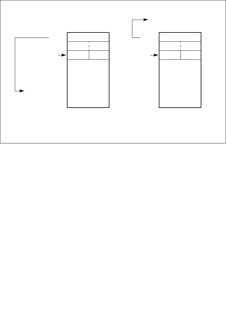
Vol. 3A 17-31
IA-32 ARCHITECTURE COMPATIBILITY
general-protection exceptions (#GP). Figure 17-1 demonstrates the different areas accessed by
the Intel486 and the P6 family and Pentium processors.
17.28. CACHE MANAGEMENT
The P6 family processors include two levels of internal caches: L1 (level 1) and L2 (level 2).
The L1 cache is divided into an instruction cache and a data cache; the L2 cache is a general-
purpose cache. See Section 10.1, “Internal Caches, TLBs, and Buffers,” for a description of
these caches. (Note that although the Pentium II processor L2 cache is physically located on a
separate chip in the cassette, it is considered an internal cache.)
The Pentium processor includes separate level 1 instruction and data caches. The data cache
supports a writeback (or alternatively write-through, on a line by line basis) policy for memory
updates.
The Intel486 processor includes a single level 1 cache for both instructions and data.
The meaning of the CD and NW flags in control register CR0 have been redefined for the P6
family and Pentium processors. For these processors, the recommended value (00B) enables
writeback for the data cache of the Pentium processor and for the L1 data cache and L2 cache
of the P6 family processors. In the Intel486 processor, setting these flags to (00B) enables write-
through for the cache.
Figure 17-1. I/O Map Base Address Differences
Intel486 Processor
FFFFH
I/O Map
Base Addres
FFFFH
FFFFH + 10H = FH
for I/O Validation
0H
FFFFH
FFFFH
I/O access at port 10H checks
0H
FFFFH + 10H = Outside Segment
for I/O Validation
bitmap at I/O address FFFFH + 10H,
which exceeds segment limit.
Wrap around does not occur,
general-protection exception (#GP)
I/O access at port 10H checks
bitmap at I/O map base address
FFFFH + 10H = offset 10H.
Offset FH from beginning of
TSS segment results because
P6 family and Pentium Processors
I/O Map
Base Addres
occurs. wraparound occurs.

17-32 Vol. 3A
IA-32 ARCHITECTURE COMPATIBILITY
External system hardware can force the Pentium processor to disable caching or to use the write-
through cache policy should that be required. In the P6 family processors, the MTRRs can be
used to override the CD and NW flags (see Table 10-6).
The P6 family and Pentium processors support page-level cache management in the same
manner as the Intel486 processor by using the PCD and PWT flags in control register CR3, the
page-directory entries, and the page-table entries. The Intel486 processor, however, is not
affected by the state of the PWT flag since the internal cache of the Intel486 processor is a write-
through cache.
17.28.1 Self-Modifying Code with Cache Enabled
On the Intel486 processor, a write to an instruction in the cache will modify it in both the cache
and memory. If the instruction was prefetched before the write, however, the old version of the
instruction could be the one executed. To prevent this problem, it is necessary to flush the
instruction prefetch unit of the Intel486 processor by coding a jump instruction immediately
after any write that modifies an instruction. The P6 family and Pentium processors, however,
check whether a write may modify an instruction that has been prefetched for execution. This
check is based on the linear address of the instruction. If the linear address of an instruction is
found to be present in the prefetch queue, the P6 family and Pentium processors flush the
prefetch queue, eliminating the need to code a jump instruction after any writes that modify an
instruction.
Because the linear address of the write is checked against the linear address of the instructions
that have been prefetched, special care must be taken for self-modifying code to work correctly
when the physical addresses of the instruction and the written data are the same, but the linear
addresses differ. In such cases, it is necessary to execute a serializing operation to flush the
prefetch queue after the write and before executing the modified instruction. See Section 7.4,
“Serializing Instructions,” for more information on serializing instructions.
NOTE
The check on linear addresses described above is not in practice a concern for
compatibility. Applications that include self-modifying code use the same
linear address for modifying and fetching the instruction. System software,
such as a debugger, that might possibly modify an instruction using a
different linear address than that used to fetch the instruction must execute a
serializing operation, such as IRET, before the modified instruction is
executed.
17.28.2 Disabling the L3 Cache
A unified third-level (L3) cache was introduced in the Pentium 4 and Intel Xeon processors (see
Section 10.1, “Internal Caches, TLBs, and Buffers”) along with the third-level cache disable
flag, bit 6 of the IA32_MISC_ENABLE MSR. The third-level cache disable flag allows the L3

Vol. 3A 17-33
IA-32 ARCHITECTURE COMPATIBILITY
cache to be disabled and enabled, independently of the L1 and L2 caches (see Section 10.5.4,
“Disabling and Enabling the L3 Cache”).
17.29. PAGING
This section identifies enhancements made to the paging mechanism and implementation differ-
ences in the paging mechanism for various IA-32 processors.
17.29.1 Large Pages
The Pentium processor extended the memory management/paging facilities of the IA-32 to
allow large (4 MBytes) pages sizes (see Section 3.6.1, “Paging Options”). The first P6 family
processor (the Pentium Pro processor) added a 2 MByte page size to the IA-32 in conjunction
with the physical address extension (PAE) feature (see Section 3.8, “36-Bit Physical Addressing
Using the PAE Paging Mechanism”).
The availability of large pages on any IA-32 processor can be determined via feature bit 3
(PSE) of register EDX after the CPUID instruction has been execution with an argument of 1.
Intel processors that do not support the CPUID instruction do not support page size enhance-
ments. (See “CPUID—CPU Identification” in Chapter 3, “Instruction Set Reference, A-M,” in
the IA-32 Intel® Architecture Software Developer’s Manual, Volume 2A, and AP-485, Intel
Processor Identification and the CPUID Instruction, for more information on the CPUID
instruction.)
17.29.2 PCD and PWT Flags
The PCD and PWT flags were introduced to the IA-32 in the Intel486 processor to control the
caching of pages:
•PCD (page-level cache disable) flag—Controls caching on a page-by-page basis.
•PWT (page-level write-through) flag—Controls the write-through/writeback caching
policy on a page-by-page basis. Since the internal cache of the Intel486 processor is a
write-through cache, it is not affected by the state of the PWT flag.
17.29.3 Enabling and Disabling Paging
Paging is enabled and disabled by loading a value into control register CR0 that modifies the PG
flag. For backward and forward compatibility with all IA-32 processors, Intel recommends that
the following operations be performed when enabling or disabling paging:
1. Execute a MOV CR0, REG instruction to either set (enable paging) or clear (disable
paging) the PG flag.
2. Execute a near JMP instruction.

17-34 Vol. 3A
IA-32 ARCHITECTURE COMPATIBILITY
The sequence bounded by the MOV and JMP instructions should be identity mapped (that is,
the instructions should reside on a page whose linear and physical addresses are identical).
For the P6 family processors, the MOV CR0, REG instruction is serializing, so the jump oper-
ation is not required. However, for backwards compatibility, the JMP instruction should still be
included.
17.30. STACK OPERATIONS
This section identifies the differences in the stack mechanism for the various IA-32 processors.
17.30.1 Selector Pushes and Pops
When pushing a segment selector onto the stack, the Pentium 4, Intel Xeon, P6 family, and
Intel486 processors decrement the ESP register by the operand size and then write 2 bytes. If the
operand size is 32-bits, the upper two bytes of the write are not modified. The Pentium processor
decrements the ESP register by the operand size and determines the size of the write by the
operand size. If the operand size is 32-bits, the upper two bytes are written as 0s.
When popping a segment selector from the stack, the Pentium 4, Intel Xeon, P6 family, and
Intel486 processors read 2 bytes and increment the ESP register by the operand size of the
instruction. The Pentium processor determines the size of the read from the operand size and
increments the ESP register by the operand size.
It is possible to align a 32-bit selector push or pop such that the operation generates an exception
on a Pentium processor and not on an Pentium 4, Intel Xeon, P6 family, or Intel486 processor.
This could occur if the third and/or fourth byte of the operation lies beyond the limit of the
segment or if the third and/or fourth byte of the operation is locate on a non-present or inacces-
sible page.
For a POP-to-memory instruction that meets the following conditions:
•The stack segment size is 16-bit.
•Any 32-bit addressing form with the SIB byte specifying ESP as the base register.
•The initial stack pointer is FFFCH (32-bit operand) or FFFEH (16-bit operand) and will
wrap around to 0H as a result of the POP operation.
The result of the memory write is implementation-specific. For example, in P6 family proces-
sors, the result of the memory write is SS:0H plus any scaled index and displacement. In
Pentium processors, the result of the memory write may be either a stack fault (real mode or
protected mode with stack segment size of 64KByte), or write to SS:10000H plus any scaled
index and displacement (protected mode and stack segment size exceeds 64KByte).

Vol. 3A 17-35
IA-32 ARCHITECTURE COMPATIBILITY
17.30.2 Error Code Pushes
The Intel486 processor implements the error code pushed on the stack as a 16-bit value. When
pushed onto a 32-bit stack, the Intel486 processor only pushes 2 bytes and updates ESP by 4.
The P6 family and Pentium processors’ error code is a full 32 bits with the upper 16 bits set to
zero. The P6 family and Pentium processors, therefore, push 4 bytes and update ESP by 4. Any
code that relies on the state of the upper 16 bits may produce inconsistent results.
17.30.3 Fault Handling Effects on the Stack
During the handling of certain instructions, such as CALL and PUSHA, faults may occur in
different sequences for the different processors. For example, during far calls, the Intel486
processor pushes the old CS and EIP before a possible branch fault is resolved. A branch fault
is a fault from a branch instruction occurring from a segment limit or access rights violation. If
a branch fault is taken, the Intel486 and P6 family processors will have corrupted memory below
the stack pointer. However, the ESP register is backed up to make the instruction restartable. The
P6 family processors issue the branch before the pushes. Therefore, if a branch fault does occur,
these processors do not corrupt memory below the stack pointer. This implementation differ-
ence, however, does not constitute a compatibility problem, as only values at or above the stack
pointer are considered to be valid.
17.30.4 Interlevel RET/IRET From a 16-Bit Interrupt or Call Gate
If a call or interrupt is made from a 32-bit stack environment through a 16-bit gate, only 16 bits
of the old ESP can be pushed onto the stack. On the subsequent RET/IRET, the 16-bit ESP is
popped but the full 32-bit ESP is updated since control is being resumed in a 32-bit stack envi-
ronment. The Intel486 processor writes the SS selector into the upper 16 bits of ESP. The P6
family and Pentium processors write zeros into the upper 16 bits.
17.31. MIXING 16- AND 32-BIT SEGMENTS
The features of the 16-bit Intel 286 processor are an object-code compatible subset of those of
the 32-bit IA-32 processors. The D (default operation size) flag in segment descriptors indicates
whether the processor treats a code or data segment as a 16-bit or 32-bit segment; the B (default
stack size) flag in segment descriptors indicates whether the processor treats a stack segment as
a 16-bit or 32-bit segment.
The segment descriptors used by the Intel 286 processor are supported by the 32-bit IA-32
processors if the Intel-reserved word (highest word) of the descriptor is clear. On the 32-bit
IA-32 processors, this word includes the upper bits of the base address and the segment limit.
The segment descriptors for data segments, code segments, local descriptor tables (there are no
descriptors for global descriptor tables), and task gates are the same for the 16- and 32-bit
processors. Other 16-bit descriptors (TSS segment, call gate, interrupt gate, and trap gate) are
supported by the 32-bit processors.

17-36 Vol. 3A
IA-32 ARCHITECTURE COMPATIBILITY
The 32-bit processors also have descriptors for TSS segments, call gates, interrupt gates, and
trap gates that support the 32-bit architecture. Both kinds of descriptors can be used in the same
system.
For those segment descriptors common to both 16- and 32-bit processors, clear bits in the
reserved word cause the 32-bit processors to interpret these descriptors exactly as an Intel 286
processor does, that is:
•Base Address — The upper 8 bits of the 32-bit base address are clear, which limits base
addresses to 24 bits.
•Limit — The upper 4 bits of the limit field are clear, restricting the value of the limit field
to 64 KBytes.
•Granularity bit — The G (granularity) flag is clear, indicating the value of the 16-bit limit
is interpreted in units of 1 byte.
•Big bit — In a data-segment descriptor, the B flag is clear in the segment descriptor used
by the 32-bit processors, indicating the segment is no larger than 64 KBytes.
•Default bit — In a code-segment descriptor, the D flag is clear, indicating 16-bit addressing
and operands are the default. In a stack-segment descriptor, the D flag is clear, indicating
use of the SP register (instead of the ESP register) and a 64-KByte maximum segment
limit.
For information on mixing 16- and 32-bit code in applications, see Chapter 16, “Mixing 16-Bit
and 32-Bit Code.”
17.32. SEGMENT AND ADDRESS WRAPAROUND
This section discusses differences in segment and address wraparound between the P6 family,
Pentium, Intel486, Intel386, Intel 286, and 8086 processors.
17.32.1 Segment Wraparound
On the 8086 processor, an attempt to access a memory operand that crosses offset 65,535 or
0FFFFH or offset 0 (for example, moving a word to offset 65,535 or pushing a word when the
stack pointer is set to 1) causes the offset to wrap around modulo 65,536 or 010000H. With the
Intel 286 processor, any base and offset combination that addresses beyond 16 MBytes wraps
around to the 1 MByte of the address space. The P6 family, Pentium, Intel486, and Intel386
processors in real-address mode generate an exception in these cases:
•A general-protection exception (#GP) if the segment is a data segment (that is, if the CS,
DS, ES, FS, or GS register is being used to address the segment).
•A stack-fault exception (#SS) if the segment is a stack segment (that is, if the SS register is
being used).

Vol. 3A 17-37
IA-32 ARCHITECTURE COMPATIBILITY
An exception to this behavior occurs when a stack access is data aligned, and the stack pointer
is pointing to the last aligned piece of data that size at the top of the stack (ESP is FFFFFFFCH).
When this data is popped, no segment limit violation occurs and the stack pointer will wrap
around to 0.
The address space of the P6 family, Pentium, and Intel486 processors may wraparound at
1 MByte in real-address mode. An external A20M# pin forces wraparound if enabled. On Intel
8086 processors, it is possible to specify addresses greater than 1 MByte. For example, with a
selector value FFFFH and an offset of FFFFH, the effective address would be 10FFEFH
(1 MByte plus 65519 bytes). The 8086 processor, which can form addresses up to 20 bits long,
truncates the uppermost bit, which “wraps” this address to FFEFH. However, the P6 family,
Pentium, and Intel486 processors do not truncate this bit if A20M# is not enabled.
If a stack operation wraps around the address limit, shutdown occurs. (The 8086 processor does
not have a shutdown mode or a limit.)
The behavior when executing near the limit of a 4-GByte selector (limit=0xFFFFFFFF) is
different between the Pentium Pro and the Pentium 4 family of processors. On the Pentium Pro,
instructions which cross the limit -- for example, a two byte instruction such as INC EAX that
is encoded as 0xFF 0xC0 starting exactly at the limit faults for a segment violation (a one byte
instruction at 0xFFFFFFFF does not cause an exception). Using the Pentium 4 microprocessor
family, neither of these situations causes a fault.
17.33. STORE BUFFERS AND MEMORY ORDERING
The Pentium 4, Intel Xeon, and P6 family processors provide a store buffer for temporary
storage of writes (stores) to memory (see Section 10.10, “Store Buffer”). Writes stored in the
store buffer(s) are always written to memory in program order, with the exception of “fast
string” store operations (see Section 7.2.3, “Out-of-Order Stores For String Operations in
Pentium 4, Intel Xeon, and P6 Family Processors”).
The Pentium processor has two store buffers, one corresponding to each of the pipelines. Writes
in these buffers are always written to memory in the order they were generated by the processor
core.
It should be noted that only memory writes are buffered and I/O writes are not. The Pentium 4,
Intel Xeon, P6 family, Pentium, and Intel486 processors do not synchronize the completion of
memory writes on the bus and instruction execution after a write. An I/O, locked, or serializing
instruction needs to be executed to synchronize writes with the next instruction (see Section 7.4,
“Serializing Instructions”).
The Pentium 4, Intel Xeon, and P6 family processors use processor ordering to maintain consis-
tency in the order that data is read (loaded) and written (stored) in a program and the order the
processor actually carries out the reads and writes. With this type of ordering, reads can be
carried out speculatively and in any order, reads can pass buffered writes, and writes to memory
are always carried out in program order. (See Section 7.2, “Memory Ordering,” for more infor-
mation about processor ordering.) The Pentium III processor introduced a new instruction to
serialize writes and make them globally visible. Memory ordering issues can arise between a
producer and a consumer of data. The SFENCE instruction provides a performance-efficient

17-38 Vol. 3A
IA-32 ARCHITECTURE COMPATIBILITY
way of ensuring ordering between routines that produce weakly-ordered results and routines that
consume this data.
No re-ordering of reads occurs on the Pentium processor, except under the condition noted in
Section 7.2.1, “Memory Ordering in the Intel® Pentium® and Intel486™ Processors,” and in
the following paragraph describing the Intel486 processor.
Specifically, the store buffers are flushed before the IN instruction is executed. No reads (as a
result of cache miss) are reordered around previously generated writes sitting in the store
buffers. The implication of this is that the store buffers will be flushed or emptied before a subse-
quent bus cycle is run on the external bus.
On both the Intel486 and Pentium processors, under certain conditions, a memory read will go
onto the external bus before the pending memory writes in the buffer even though the writes
occurred earlier in the program execution. A memory read will only be reordered in front of all
writes pending in the buffers if all writes pending in the buffers are cache hits and the read is a
cache miss. Under these conditions, the Intel486 and Pentium processors will not read from an
external memory location that needs to be updated by one of the pending writes.
During a locked bus cycle, the Intel486 processor will always access external memory, it will
never look for the location in the on-chip cache. All data pending in the Intel486 processor's
store buffers will be written to memory before a locked cycle is allowed to proceed to the
external bus. Thus, the locked bus cycle can be used for eliminating the possibility of reordering
read cycles on the Intel486 processor. The Pentium processor does check its cache on a read-
modify-write access and, if the cache line has been modified, writes the contents back to
memory before locking the bus. The P6 family processors write to their cache on a read-modify-
write operation (if the access does not split across a cache line) and does not write back to system
memory. If the access does split across a cache line, it locks the bus and accesses system
memory.
I/O reads are never reordered in front of buffered memory writes on an IA-32 processor. This
ensures an update of all memory locations before reading the status from an I/O device.
17.34. BUS LOCKING
The Intel 286 processor performs the bus locking differently than the Intel P6 family, Pentium,
Intel486, and Intel386 processors. Programs that use forms of memory locking specific to the
Intel 286 processor may not run properly when run on later processors.
A locked instruction is guaranteed to lock only the area of memory defined by the destination
operand, but may lock a larger memory area. For example, typical 8086 and Intel 286 configu-
rations lock the entire physical memory space. Programmers should not depend on this.
On the Intel 286 processor, the LOCK prefix is sensitive to IOPL. If the CPL is greater than the
IOPL, a general-protection exception (#GP) is generated. On the Intel386 DX, Intel486, and
Pentium, and P6 family processors, no check against IOPL is performed.
The Pentium processor automatically asserts the LOCK# signal when acknowledging external
interrupts. After signaling an interrupt request, an external interrupt controller may use the data

Vol. 3A 17-39
IA-32 ARCHITECTURE COMPATIBILITY
bus to send the interrupt vector to the processor. After receiving the interrupt request signal, the
processor asserts LOCK# to insure that no other data appears on the data bus until the interrupt
vector is received. This bus locking does not occur on the P6 family processors.
17.35. BUS HOLD
Unlike the 8086 and Intel 286 processors, but like the Intel386 and Intel486 processors, the P6
family and Pentium processors respond to requests for control of the bus from other potential
bus masters, such as DMA controllers, between transfers of parts of an unaligned operand, such
as two words which form a doubleword. Unlike the Intel386 processor, the P6 family, Pentium
and Intel486 processors respond to bus hold during reset initialization.
17.36. MODEL-SPECIFIC EXTENSIONS TO THE IA-32
Certain extensions to the IA-32 are specific to a processor or family of IA-32 processors and
may not be implemented or implemented in the same way in future processors. The following
sections describe these model-specific extensions. The CPUID instruction indicates the avail-
ability of some of the model-specific features.
17.36.1 Model-Specific Registers
The Pentium processor introduced a set of model-specific registers (MSRs) for use in control-
ling hardware functions and performance monitoring. To access these MSRs, two new instruc-
tions were added to the IA-32 architecture: read MSR (RDMSR) and write MSR (WRMSR).
The MSRs in the Pentium processor are not guaranteed to be duplicated or provided in the next
generation IA-32 processors.
The P6 family processors greatly increased the number of MSRs available to software. See
Appendix B, “Model-Specific Registers (MSRs),” for a complete list of the available MSRs.
The new registers control the debug extensions, the performance counters, the machine-check
exception capability, the machine-check architecture, and the MTRRs. These registers are
accessible using the RDMSR and WRMSR instructions. Specific information on some of these
new MSRs is provided in the following sections. As with the Pentium processor MSR, the P6
family processor MSRs are not guaranteed to be duplicated or provided in the next generation
IA-32 processors.
17.36.2 RDMSR and WRMSR Instructions
The RDMSR (read model-specific register) and WRMSR (write model-specific register)
instructions recognize a much larger number of model-specific registers in the P6 family proces-
sors. (See “RDMSR—Read from Model Specific Register” and “WRMSR—Write to Model
Specific Register” in the IA-32 Intel® Architecture Software Developer’s Manual, Volumes
2A & 2B for more information.)

17-40 Vol. 3A
IA-32 ARCHITECTURE COMPATIBILITY
17.36.3 Memory Type Range Registers
Memory type range registers (MTRRs) are a new feature introduced into the IA-32 in the
Pentium Pro processor. MTRRs allow the processor to optimize memory operations for different
types of memory, such as RAM, ROM, frame buffer memory, and memory-mapped I/O.
MTRRs are MSRs that contain an internal map of how physical address ranges are mapped to
various types of memory. The processor uses this internal memory map to determine the cache-
ability of various physical memory locations and the optimal method of accessing memory loca-
tions. For example, if a memory location is specified in an MTRR as write-through memory, the
processor handles accesses to this location as follows. It reads data from that location in lines
and caches the read data or maps all writes to that location to the bus and updates the cache to
maintain cache coherency. In mapping the physical address space with MTRRs, the processor
recognizes five types of memory: uncacheable (UC), uncacheable, speculatable, write-
combining (USWC), write-through (WT), write-protected (WP), and writeback (WB).
Earlier IA-32 processors (such as the Intel486 and Pentium processors) used the KEN# (cache
enable) pin and external logic to maintain an external memory map and signal cacheable
accesses to the processor. The MTRR mechanism simplifies hardware designs by eliminating
the KEN# pin and the external logic required to drive it.
See Chapter 9, “Processor Management and Initialization,” and Appendix B, “Model-Specific
Registers (MSRs),” for more information on the MTRRs.
17.36.4 Machine-Check Exception and Architecture
The Pentium processor introduced a new exception called the machine-check exception (#MC,
interrupt 18). This exception is used to detect hardware-related errors, such as a parity error on
a read cycle.
The P6 family processors extend the types of errors that can be detected and that generate a
machine-check exception. It also provides a new machine-check architecture for recording
information about a machine-check error and provides extended recovery capability.
The machine-check architecture provides several banks of reporting registers for recording
machine-check errors. Each bank of registers is associated with a specific hardware unit in the
processor. The primary focus of the machine checks is on bus and interconnect operations;
however, checks are also made of translation lookaside buffer (TLB) and cache operations.
The machine-check architecture can correct some errors automatically and allow for reliable
restart of instruction execution. It also collects sufficient information for software to use in
correcting other machine errors not corrected by hardware.
See Chapter 14, “Machine-Check Architecture,” for more information on the machine-check
exception and the machine-check architecture.

Vol. 3A 17-41
IA-32 ARCHITECTURE COMPATIBILITY
17.36.5 Performance-Monitoring Counters
The P6 family and Pentium processors provide two performance-monitoring counters for use in
monitoring internal hardware operations. These counters are event counters that can be
programmed to count a variety of different types of events, such as the number of instructions
decoded, number of interrupts received, or number of cache loads. Appendix A, “Performance-
Monitoring Events,” lists all the events that can be counted (Table A-12 for the P6 family
processors and Table A-13 for the Pentium processors). The counters are set up, started, and
stopped using two MSRs and the RDMSR and WRMSR instructions. For the P6 family proces-
sors, the current count for a particular counter can be read using the new RDPMC instruction.
The performance-monitoring counters are useful for debugging programs, optimizing code,
diagnosing system failures, or refining hardware designs. See Chapter 18, “Debugging and
Performance Monitoring,” for more information on these counters.
17.37. TWO WAYS TO RUN INTEL 286 PROCESSOR TASKS
When porting 16-bit programs to run on 32-bit IA-32 processors, there are two approaches
to consider:
•Porting an entire 16-bit software system to a 32-bit processor, complete with the old
operating system, loader, and system builder. Here, all tasks will have 16-bit TSSs. The
32-bit processor is being used as if it were a faster version of the 16-bit processor.
•Porting selected 16-bit applications to run in a 32-bit processor environment with a 32-bit
operating system, loader, and system builder. Here, the TSSs used to represent 286 tasks
should be changed to 32-bit TSSs. It is possible to mix 16 and 32-bit TSSs, but the benefits
are small and the problems are great. All tasks in a 32-bit software system should have
32-bit TSSs. It is not necessary to change the 16-bit object modules themselves; TSSs are
usually constructed by the operating system, by the loader, or by the system builder. See
Chapter 16, “Mixing 16-Bit and 32-Bit Code,” for more detailed information about mixing
16-bit and 32-bit code.
Because the 32-bit processors use the contents of the reserved word of 16-bit segment descrip-
tors, 16-bit programs that place values in this word may not run correctly on the 32-bit
processors.

17-42 Vol. 3A
IA-32 ARCHITECTURE COMPATIBILITY

INTEL SALES OFFICES
ASIA PACIFIC
Australia
Intel Corp.
Level 2
448 St Kilda Road
Melbourne VIC
3004
Australia
Fax:613-9862 5599
China
Intel Corp.
Rm 709, Shaanxi
Zhongda Int'l Bldg
No.30 Nandajie Street
Xian AX710002
China
Fax:(86 29) 7203356
Intel Corp.
Rm 2710, Metropolian
Tower
68 Zourong Rd
Chongqing CQ
400015
China
Intel Corp.
C1, 15 Flr, Fujian
Oriental Hotel
No. 96 East Street
Fuzhou FJ
350001
China
Intel Corp.
Rm 5803 CITIC Plaza
233 Tianhe Rd
Guangzhou GD
510613
China
Intel Corp.
Rm 1003, Orient Plaza
No. 235 Huayuan Street
Nangang District
Harbin HL
150001
China
Intel Corp.
Rm 1751 World Trade
Center, No 2
Han Zhong Rd
Nanjing JS
210009
China
Intel Corp.
Hua Xin International
Tower
215 Qing Nian St.
ShenYang LN
110015
China
Intel Corp.
Suite 1128 CITIC Plaza
Jinan
150 Luo Yuan St.
Jinan SN
China
Intel Corp.
Suite 412, Holiday Inn
Crowne Plaza
31, Zong Fu Street
Chengdu SU
610041
China
Fax:86-28-6785965
Intel Corp.
Room 0724, White Rose
Hotel
No 750, MinZhu Road
WuChang District
Wuhan UB
430071
China
India
Intel Corp.
Paharpur Business
Centre
21 Nehru Place
New Delhi DH
110019
India
Intel Corp.
Hotel Rang Sharda, 6th
Floor
Bandra Reclamation
Mumbai MH
400050
India
Fax:91-22-6415578
Intel Corp.
DBS Corporate Club
31A Cathedral Garden
Road
Chennai TD
600034
India
Intel Corp.
DBS Corporate Club
2nd Floor, 8 A.A.C. Bose
Road
Calcutta WB
700017
India
Japan
Intel Corp.
Kokusai Bldg 5F, 3-1-1,
Marunouchi
Chiyoda-Ku, Tokyo
1000005
Japan
Intel Corp.
2-4-1 Terauchi
Toyonaka-Shi
Osaka
5600872
Japan
Malaysia
Intel Corp.
Lot 102 1/F Block A
Wisma Semantan
12 Jalan Gelenggang
Damansara Heights
Kuala Lumpur SL
50490
Malaysia
Thailand
Intel Corp.
87 M. Thai Tower, 9th Fl.
All Seasons Place,
Wireless Road
Lumpini, Patumwan
Bangkok
10330
Thailand
Viet Nam
Intel Corp.
Hanoi Tung Shing
Square, Ste #1106
2 Ngo Quyen St
Hoan Kiem District
Hanoi
Viet Nam
EUROPE & AFRICA
Belgium
Intel Corp.
Woluwelaan 158
Diegem
1831
Belgium
Czech Rep
Intel Corp.
Nahorni 14
Brno
61600
Czech Rep
Denmark
Intel Corp.
Soelodden 13
Maaloev
DK2760
Denmark
Germany
Intel Corp.
Sandstrasse 4
Aichner
86551
Germany
Intel Corp.
Dr Weyerstrasse 2
Juelich
52428
Germany
Intel Corp.
Buchenweg 4
Wildberg
72218
Germany
Intel Corp.
Kemnader Strasse 137
Bochum
44797
Germany
Intel Corp.
Klaus-Schaefer Strasse
16-18
Erfstadt NW
50374
Germany
Intel Corp.
Heldmanskamp 37
Lemgo NW
32657
Germany
Italy
Intel Corp Italia Spa
Milanofiori Palazzo E/4
Assago
Milan
20094
Italy
Fax:39-02-57501221
Netherland
Intel Corp.
Strausslaan 31
Heesch
5384CW
Netherland
Poland
Intel Poland
Developments, Inc
Jerozolimskie Business
Park
Jerozolimskie 146c
Warsaw
2305
Poland
Fax:+48-22-570 81 40
Portugal
Intel Corp.
PO Box 20
Alcabideche
2765
Portugal
Spain
Intel Corp.
Calle Rioja, 9
Bajo F Izquierda
Madrid
28042
Spain
South Africa
Intel SA Corporation
Bldg 14, South Wing,
2nd Floor
Uplands, The Woodlands
Western Services Road
Woodmead
2052
Sth Africa
Fax:+27 11 806 4549
Intel Corp.
19 Summit Place,
Halfway House
Cnr 5th and Harry
Galaun Streets
Midrad
1685
Sth Africa
United Kingdom
Intel Corp.
The Manse
Silver Lane
Needingworth CAMBS
PE274SL
UK
Intel Corp.
2 Cameron Close
Long Melford SUFFK
CO109TS
UK
Israel
Intel Corp.
MTM Industrial Center,
P.O.Box 498
Haifa
31000
Israel
Fax:972-4-8655444
LATIN AMERICA &
CANADA
Argentina
Intel Corp.
Dock IV - Bldg 3 - Floor 3
Olga Cossettini 240
Buenos Aires
C1107BVA
Argentina
Brazil
Intel Corp.
Rua Carlos Gomez
111/403
Porto Alegre
90480-003
Brazil
Intel Corp.
Av. Dr. Chucri Zaidan
940 - 10th Floor
San Paulo
04583-904
Brazil
Intel Corp.
Av. Rio Branco,
1 - Sala 1804
Rio de Janeiro
20090-003
Brazil
Columbia
Intel Corp.
Carrera 7 No. 71021
Torre B, Oficina 603
Santefe de Bogota
Columbia
Mexico
Intel Corp.
Av. Mexico No. 2798-9B,
S.H.
Guadalajara
44680
Mexico
Intel Corp.
Torre Esmeralda II,
7th Floor
Blvd. Manuel Avila
Comacho #36
Mexico Cith DF
11000
Mexico
Intel Corp.
Piso 19, Suite 4
Av. Batallon de San
Patricio No 111
Monterrey, Nuevo le
66269
Mexico
Canada
Intel Corp.
168 Bonis Ave, Suite 202
Scarborough
MIT3V6
Canada
Fax:416-335-7695
Intel Corp.
3901 Highway #7,
Suite 403
Vaughan
L4L 8L5
Canada
Fax:905-856-8868

Intel Corp.
999 CANADA PLACE,
Suite 404,#11
Vancouver BC
V6C 3E2
Canada
Fax:604-844-2813
Intel Corp.
2650 Queensview Drive,
Suite 250
Ottawa ON
K2B 8H6
Canada
Fax:613-820-5936
Intel Corp.
190 Attwell Drive,
Suite 500
Rexcdale ON
M9W 6H8
Canada
Fax:416-675-2438
Intel Corp.
171 St. Clair Ave. E,
Suite 6
Toronto ON
Canada
Intel Corp.
1033 Oak Meadow Road
Oakville ON
L6M 1J6
Canada
USA
California
Intel Corp.
551 Lundy Place
Milpitas CA
95035-6833
USA
Fax:408-451-8266
Intel Corp.
1551 N. Tustin Avenue,
Suite 800
Santa Ana CA
92705
USA
Fax:714-541-9157
Intel Corp.
Executive Center del Mar
12230 El Camino Real
Suite 140
San Diego CA
92130
USA
Fax:858-794-5805
Intel Corp.
1960 E. Grand Avenue,
Suite 150
El Segundo CA
90245
USA
Fax:310-640-7133
Intel Corp.
23120 Alicia Parkway,
Suite 215
Mission Viejo CA
92692
USA
Fax:949-586-9499
Intel Corp.
30851 Agoura Road
Suite 202
Agoura Hills CA
91301
USA
Fax:818-874-1166
Intel Corp.
28202 Cabot Road,
Suite #363 & #371
Laguna Niguel CA
92677
USA
Intel Corp.
657 S Cendros Avenue
Solana Beach CA
90075
USA
Intel Corp.
43769 Abeloe Terrace
Fremont CA
94539
USA
Intel Corp.
1721 Warburton, #6
Santa Clara CA
95050
USA
Colorado
Intel Corp.
600 S. Cherry Street,
Suite 700
Denver CO
80222
USA
Fax:303-322-8670
Connecticut
Intel Corp.
Lee Farm Corporate Pk
83 Wooster Heights
Road
Danbury CT
6810
USA
Fax:203-778-2168
Florida
Intel Corp.
7777 Glades Road
Suite 310B
Boca Raton FL
33434
USA
Fax:813-367-5452
Georgia
Intel Corp.
20 Technology Park,
Suite 150
Norcross GA
30092
USA
Fax:770-448-0875
Intel Corp.
Three Northwinds Center
2500 Northwinds
Parkway, 4th Floor
Alpharetta GA
30092
USA
Fax:770-663-6354
Idaho
Intel Corp.
910 W. Main Street, Suite
236
Boise ID
83702
USA
Fax:208-331-2295
Illinois
Intel Corp.
425 N. Martingale Road
Suite 1500
Schaumburg IL
60173
USA
Fax:847-605-9762
Intel Corp.
999 Plaza Drive
Suite 360
Schaumburg IL
60173
USA
Intel Corp.
551 Arlington Lane
South Elgin IL
60177
USA
Indiana
Intel Corp.
9465 Counselors Row,
Suite 200
Indianapolis IN
46240
USA
Fax:317-805-4939
Massachusetts
Intel Corp.
125 Nagog Park
Acton MA
01720
USA
Fax:978-266-3867
Intel Corp.
59 Composit Way
suite 202
Lowell MA
01851
USA
Intel Corp.
800 South Street,
Suite 100
Waltham MA
02154
USA
Maryland
Intel Corp.
131 National Business
Parkway, Suite 200
Annapolis Junction MD
20701
USA
Fax:301-206-3678
Michigan
Intel Corp.
32255 Northwestern
Hwy., Suite 212
Farmington Hills MI
48334
USA
Fax:248-851-8770
MInnesota
Intel Corp.
3600 W 80Th St
Suite 450
Bloomington MN
55431
USA
Fax:952-831-6497
North Carolina
Intel Corp.
2000 CentreGreen Way,
Suite 190
Cary NC
27513
USA
Fax:919-678-2818
New Hampshire
Intel Corp.
7 Suffolk Park
Nashua NH
03063
USA
New Jersey
Intel Corp.
90 Woodbridge Center
Dr, Suite. 240
Woodbridge NJ
07095
USA
Fax:732-602-0096
New York
Intel Corp.
628 Crosskeys Office Pk
Fairport NY
14450
USA
Fax:716-223-2561
Intel Corp.
888 Veterans Memorial
Highway
Suite 530
Hauppauge NY
11788
USA
Fax:516-234-5093
Ohio
Intel Corp.
3401 Park Center Drive
Suite 220
Dayton OH
45414
USA
Fax:937-890-8658
Intel Corp.
56 Milford Drive
Suite 205
Hudson OH
44236
USA
Fax:216-528-1026
Oregon
Intel Corp.
15254 NW Greenbrier
Parkway, Building B
Beaverton OR
97006
USA
Fax:503-645-8181
Pennsylvania
Intel Corp.
925 Harvest Drive
Suite 200
Blue Bell PA
19422
USA
Fax:215-641-0785
Intel Corp.
7500 Brooktree
Suite 213
Wexford PA
15090
USA
Fax:714-541-9157
Texas
Intel Corp.
5000 Quorum Drive,
Suite 750
Dallas TX
75240
USA
Fax:972-233-1325
Intel Corp.
20445 State Highway
249, Suite 300
Houston TX
77070
USA
Fax:281-376-2891
Intel Corp.
8911 Capital of Texas
Hwy, Suite 4230
Austin TX
78759
USA
Fax:512-338-9335
Intel Corp.
7739 La Verdura Drive
Dallas TX
75248
USA
Intel Corp.
77269 La Cabeza Drive
Dallas TX
75249
USA
Intel Corp.
3307 Northland Drive
Austin TX
78731
USA
Intel Corp.
15190 Prestonwood
Blvd. #925
Dallas TX
75248
USA
Intel Corp.
Washington
Intel Corp.
2800 156Th Ave. SE
Suite 105
Bellevue WA
98007
USA
Fax:425-746-4495
Intel Corp.
550 Kirkland Way
Suite 200
Kirkland WA
98033
USA
Wisconsin
Intel Corp.
405 Forest Street
Suites 109/112
Oconomowoc Wi
53066
USA
