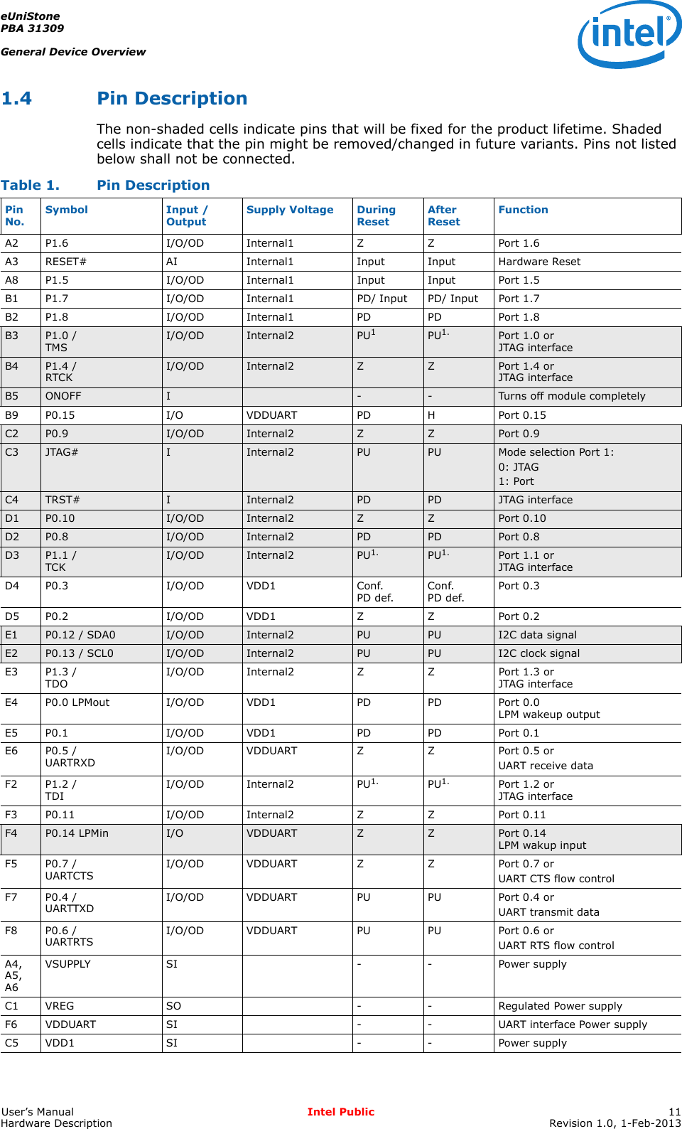
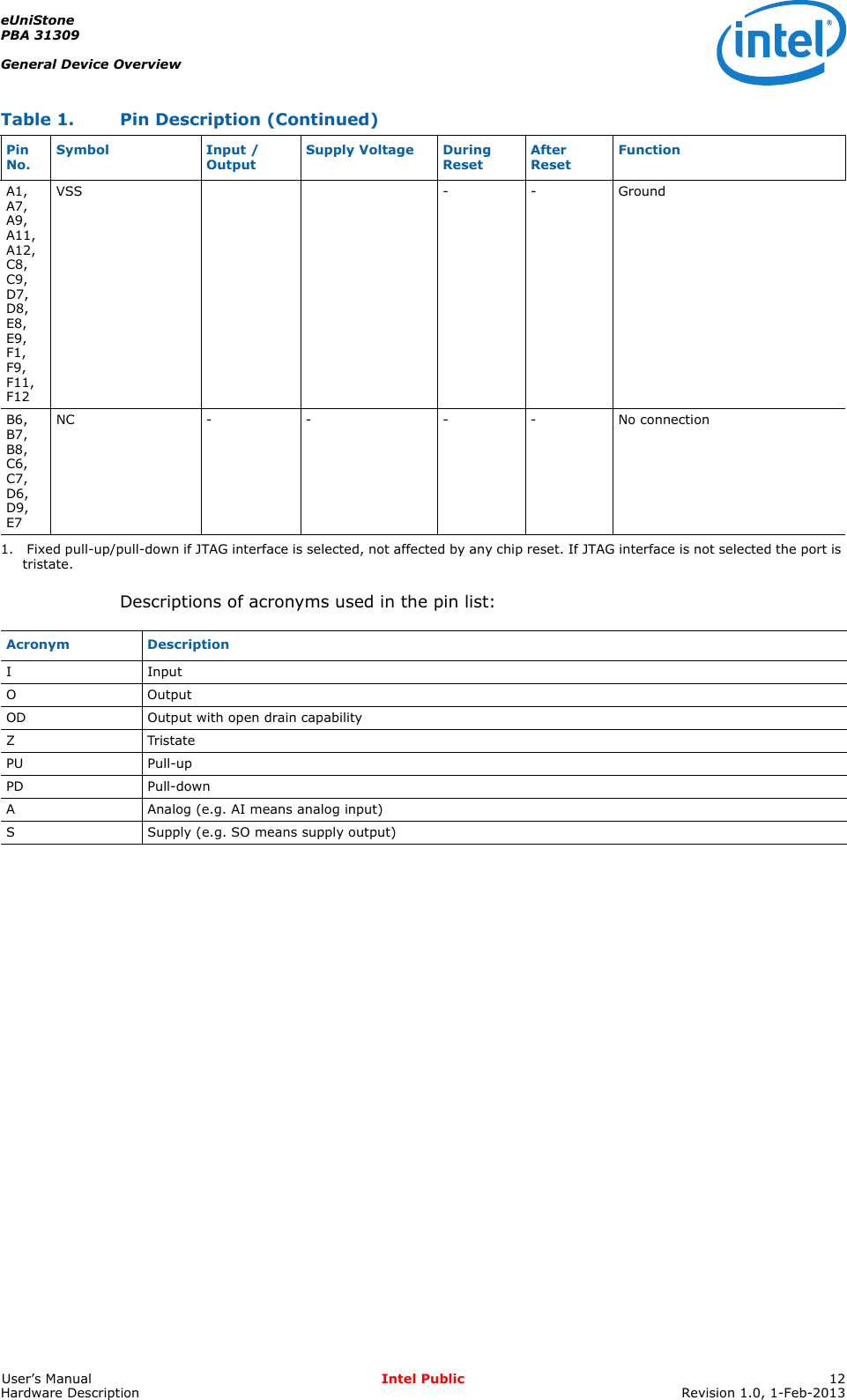
Intel PBA31309 Bluetooth Wireless Adapter User Manual
Intel Mobile Communications Bluetooth Wireless Adapter
UserManual.wiki
>
Intel
>
PBA31309 User Manual
User Manual
Navigation menu
Upload a User Manual
Namespaces
Wiki Guide
HTML
PDF
Info
Views
User Manual
Discussion / Help
Navigation

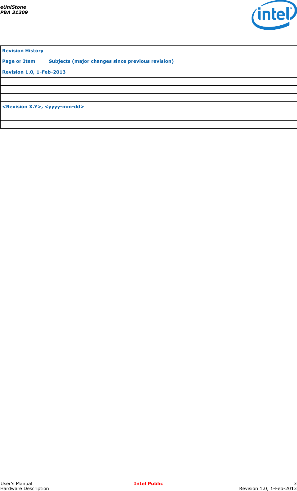
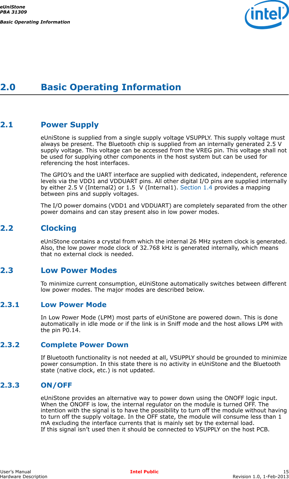
![eUniStonePBA 31309eUniStone InterfacesUser’s Manual Intel Public 16Hardware Description Revision 1.0, 1-Feb-20133.0 eUniStone Interfaces3.1 UART InterfaceThe UART interface is the main communication interface between the host and eUniStone. AT commands are described in detail in the AT Commands specification [1].The interface consists of four UART signals and two LPM control signals as shown in Figure 4.Figure 4. UART Interface3.1.1 UARTThe lines UARTTXD and UARTRXD are used for commands, responses and data. The lines UARTRTS and UARTCTS are used for hardware flow control. A separate supply voltage, VDDUART, defines the UART reference levels to fit any system requirements.3.1.1.1 Baud RatesThe UART baud rate can be configured with the BD_DATA parameter UART_Baudrate. The module is programmed for a default baudrate of 115200 baud. Reprogramming of the EEPROM configuration is possible by AT commands at manufacturing time of the end product. The baudrate written to EEPROM will be used each time eUniStone starts or, HW or SW reset is done.The host is also able to change the baudrate temporarily with an AT command. This baudrate is used by eUniStone until a HW or SW reset is done, when it will change back to the baudrate stored in the EEPROM.eUnistone_UART_Interface.vsdUARTTXDUARTRXDUARTRTSUARTCTSWAKEUP_BTWAKEUP_HOSTUARTTXDUARTRXDUARTRTSUARTCTSP0.14 inputP0.0 outputHost eUniStone](https://usermanual.wiki/Intel/PBA31309/User-Guide-2068717-Page-16.png)
![eUniStonePBA 31309General Device CapabilitiesUser’s Manual Intel Public 19Hardware Description Revision 1.0, 1-Feb-20134.0 General Device CapabilitiesThis chapter describes features available in the eUniStone (PBA 31309).Actual feature set and how to access the features can be found in the AT Command document [1]. Release specific performance characteristics, data throughput and current consumption are listed in the SW Release Notes [2].4.1 RF Test ApplicationThe eUniStone module can be programmed over UART with a specific application for RF test purposes, e.g. TX continuous or TX burst mode. This test application is controlled over the UART through Intel specific HCI commands. The commands supported by this test application are described in the document “T8753-2-Intel_Specific_HCI_Commands-7600.pdf”.4.2 Firmware ROM PatchingIn any chip with complex firmware in ROM it is wise to support patching. The risk of project delay is significantly reduced when problems can be solved without hardware changes. Enhancements, adaptations and bug fixes can be handled very late during design-in, even after the chip has been soldered in the final product.The well-proven patch concept used in BlueMoon UniCellular is described below.4.2.1 Patch SupportThe Bluetooth chip contains dedicated hardware that makes it possible to apply patches to the code and data in the firmware ROM. The hardware is capable of replacing up to 32 blocks of 16 bytes each with new content. This area can be filled with any combination of code and data. The firmware patch is stored in EEPROM and automatically loaded after startup. This provides a flexible bugfix solution for the software in ROM.](https://usermanual.wiki/Intel/PBA31309/User-Guide-2068717-Page-19.png)
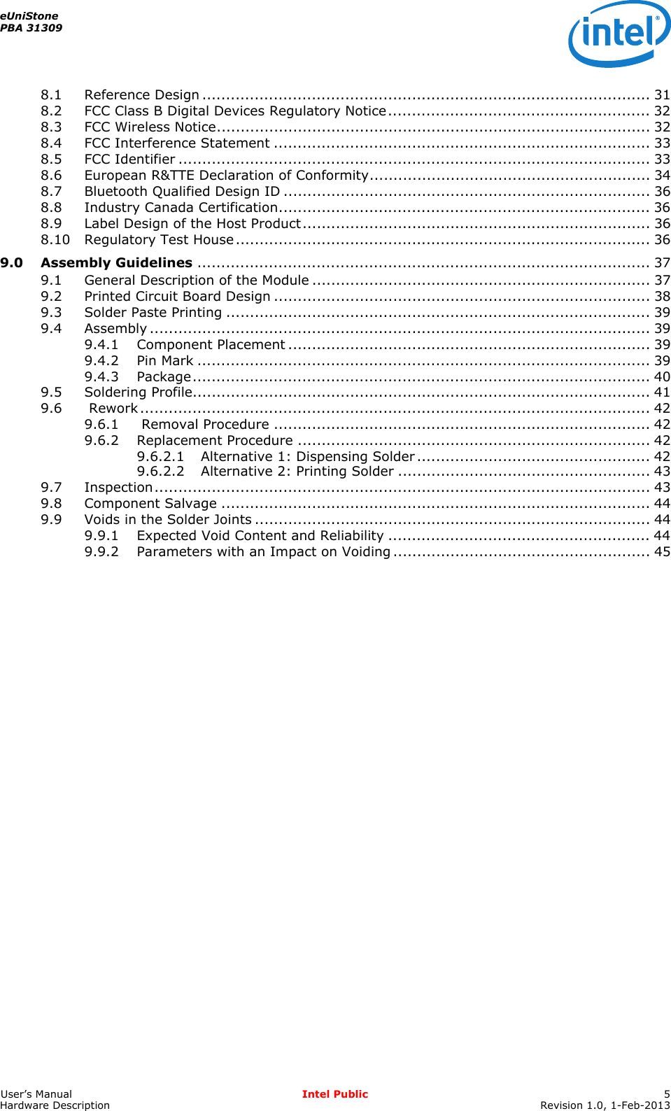
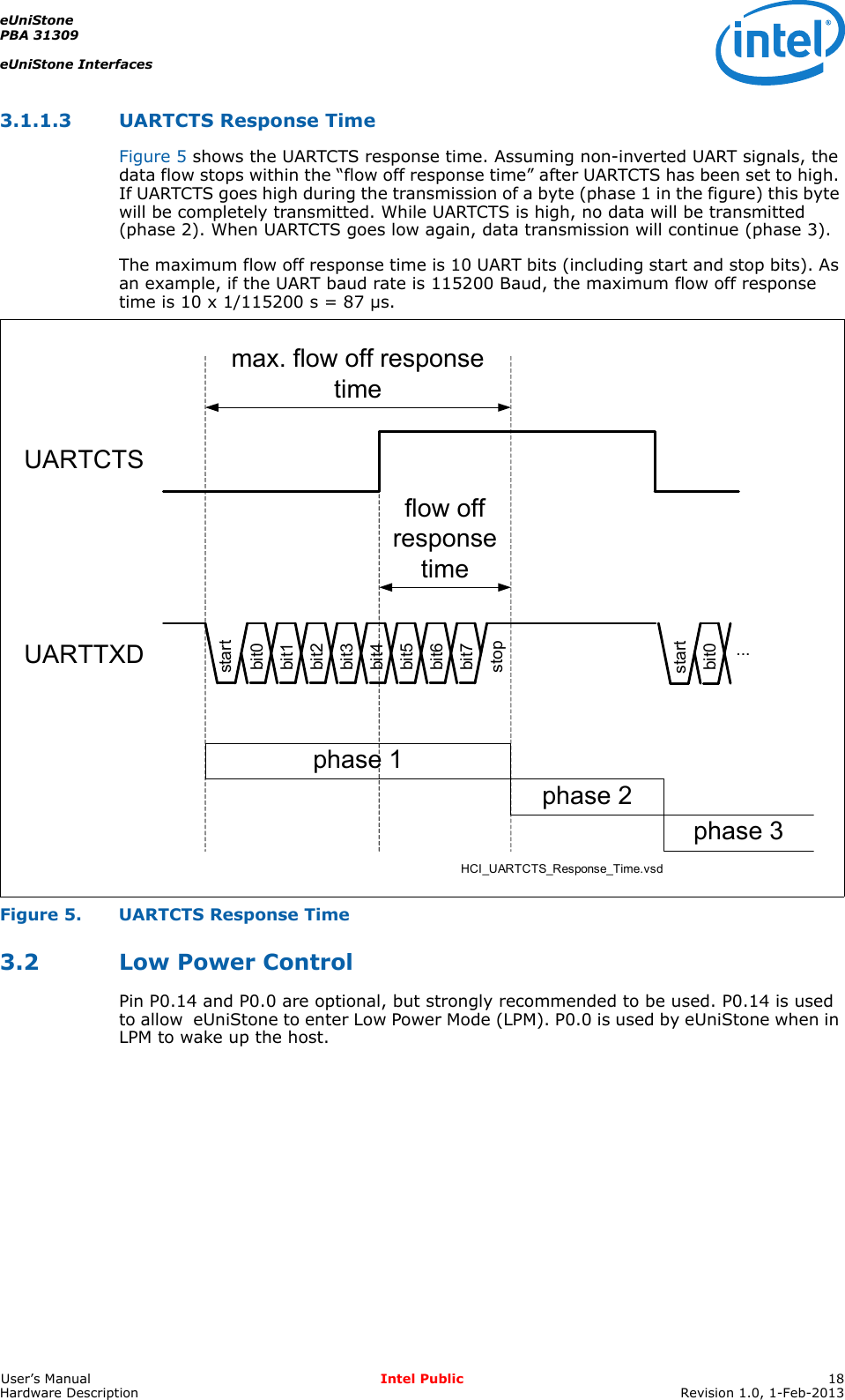
![eUniStonePBA 31309Electrical CharacteristicsUser’s Manual Intel Public 26Hardware Description Revision 1.0, 1-Feb-20136.3.4 System Power ConsumptionNote: I/O currents are not included since they depend mainly on external loads. For more details see [2].6.4 RF Part6.4.1 Characteristics RF PartThe characteristics involve the spread of values to be within the specific temperature range. Typical characteristics are the median of the production.All values refers to Intel reference design.6.4.1.1 Bluetooth Related SpecificationsTable 12. Max. Load at the Different Supply VoltagesParameter Symbol Values Unit Note / Test ConditionMin. Typ. Max.Vsupply – – 100 mA Peak currentTable 13. BDR - Transmitter PartParameter Symbol Values Unit Note / Test ConditionMin. Typ. Max.Output power (high gain) 0.5 2.5 4.5 dBm Default settingsOutput power (highest gain) – 4.5 – dBm Maximum settingsPower control step size 4 6 8 dB –Frequency range fL 2400 2401.3 – MHz –Frequency range fH – 2480.7 2483.5 MHz –20 dB bandwidth – 0.930 1 MHz –2nd adjacent channel power – -40 -20 dBm –3rd adjacent channel power – -60 -40 dBm –>3rd adjacent channel power – -64 -40 dBm Max. 2 of 3 exceptions @ 52 MHz offset might be usedAverage modulation deviation for 00001111 sequence 140 156 175 kHz –Minimum modulation deviation for 01010101 sequence 115 145 – kHz –Ratio Deviation 01010101 / Deviation 00001111 0.8 1 – –Initial carrier frequency tolerance |foffset| –– 75 kHz –Carrier frequency drift (one slot) |fdrift| –1025 kHz –Carrier frequency drift (three slots) |fdrift| –1040 kHz –Carrier frequency drift (five slots) |fdrift| –1040 kHz –Carrier frequency driftrate (one slot) |fdriftrate| – 5 20 kHz/50 ms –](https://usermanual.wiki/Intel/PBA31309/User-Guide-2068717-Page-26.png)
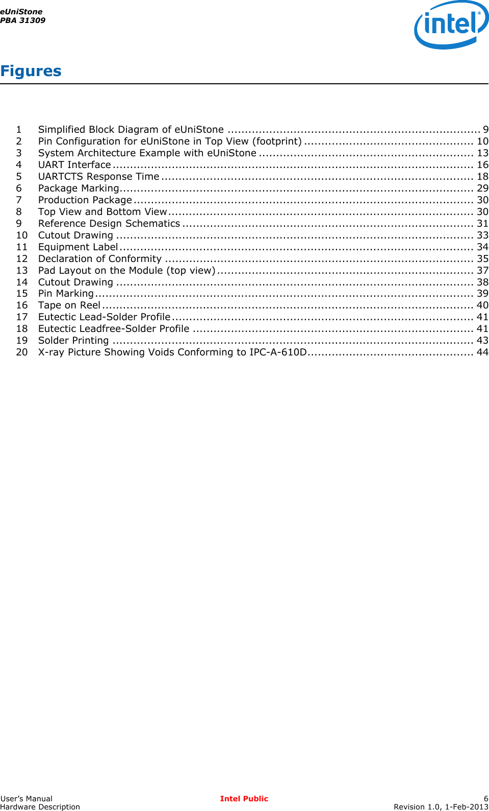
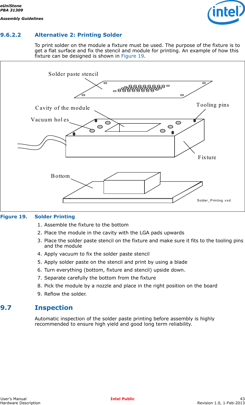
![eUniStonePBA 31309Assembly GuidelinesUser’s Manual Intel Public 41Hardware Description Revision 1.0, 1-Feb-20139.5 Soldering ProfileGenerally all standard reflow soldering processes (vapour phase, convection, infrared) and typical temperature profiles used for surface mount devices are suitable for the eUniStone module. Wave soldering is not possible.Figure 17 and Figure 18 shows example of a suitable solder reflow profile. One for leaded and one for leadfree solder.Figure 17. Eutectic Lead-Solder ProfileFigure 18. Eutectic Leadfree-Solder ProfileLead_Solder_Profile .vsd Recommended temp. profile for reflow soldering Temp.[°C] Time [s] 235°C max. 220 5°C 200°C150 10°C 90 30s 10 1s 30 +20/-10s LeadFree_Solder_Profile.vsd 25°C 150°C 200°C 217°C 255°C 260°C 60 ~ 120 sec @ 3’C/sec max60 ~ 150 sec30 sec max 6’C/sec max 8 minutes maxTemp.[°C] Time [s] Recommended temp. profile for reflow soldering (J-STD-020C)](https://usermanual.wiki/Intel/PBA31309/User-Guide-2068717-Page-41.png)
![eUniStonePBA 31309User’s Manual Intel Public 46Hardware Description Revision 1.0, 1-Feb-2013References[1] Intel AT Command Specification (eUniStone_1.00_UM_SD.pdf)[2] Release Notes for SPP AT application SW version 1.1 (eUniStone_1.00_SW_3.1_RN.pdf)](https://usermanual.wiki/Intel/PBA31309/User-Guide-2068717-Page-46.png)