Itron 0001 User Manual c2xt hwigbook
Itron c2xt hwigbook
UserManual.wiki
>
Itron
>
0001 User Manual
User Manual
Navigation menu
Upload a User Manual
Namespaces
Wiki Guide
HTML
PDF
Info
Views
User Manual
Discussion / Help
Navigation


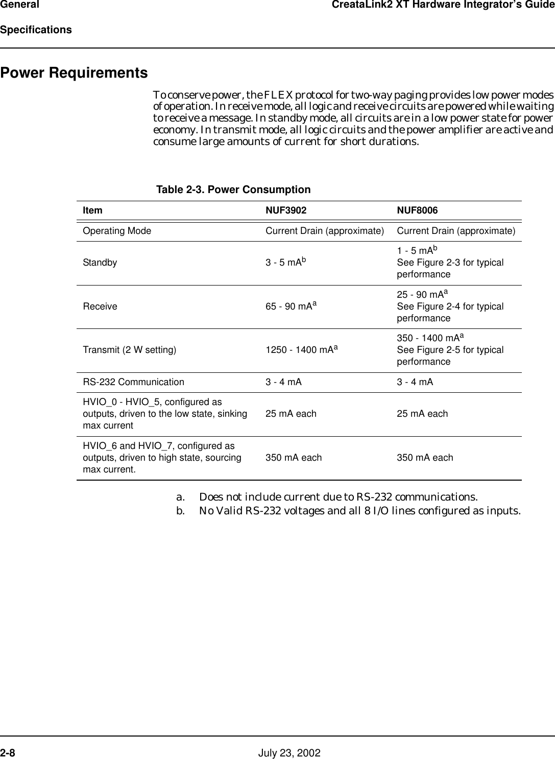
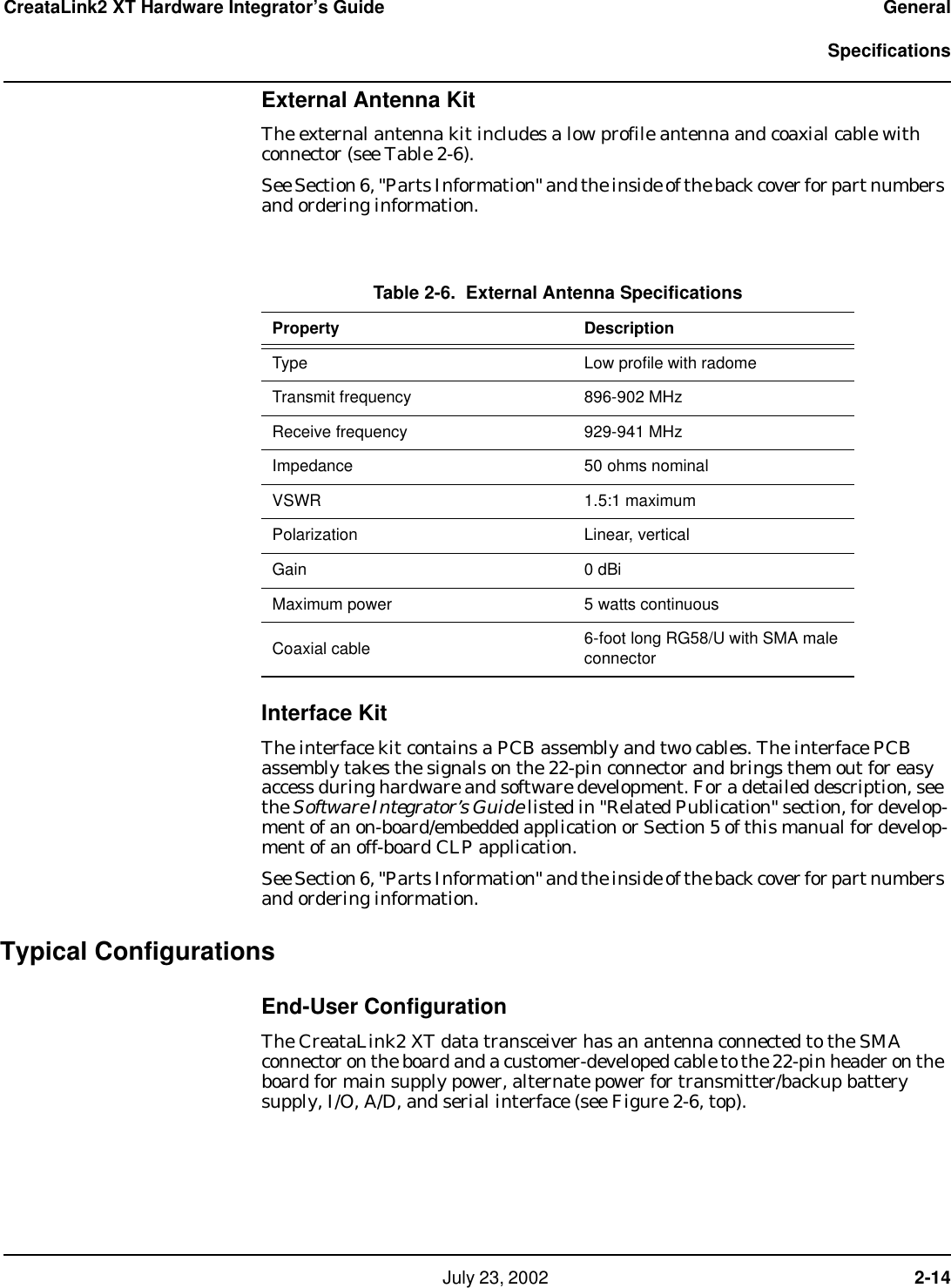
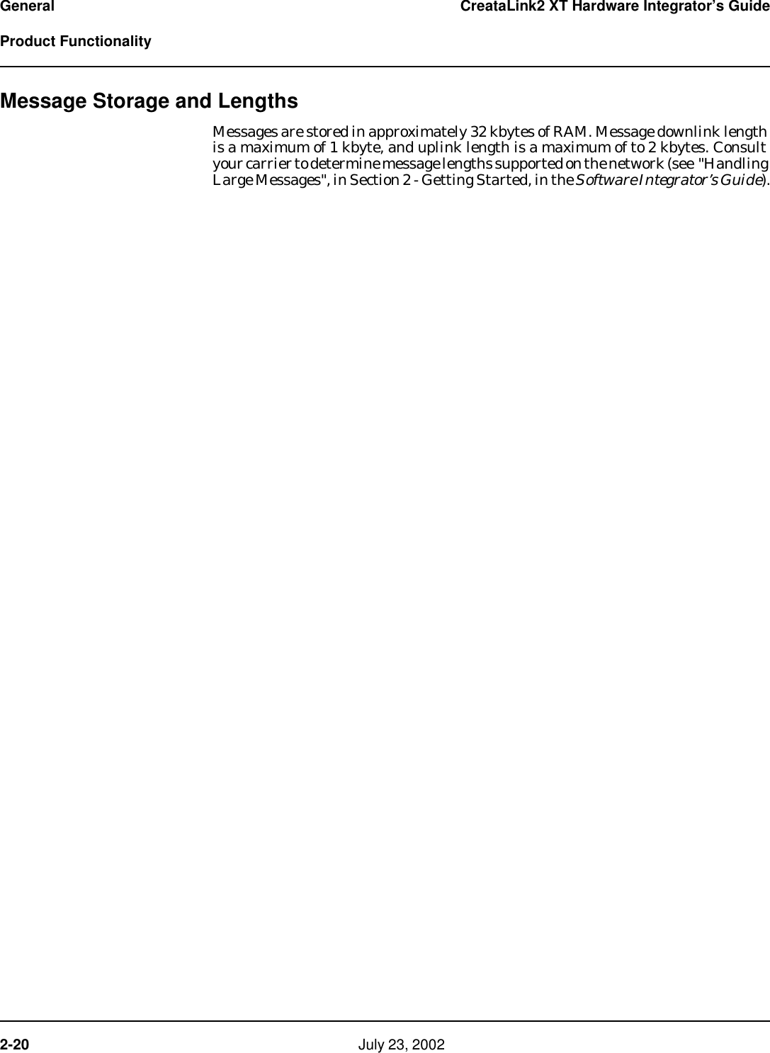

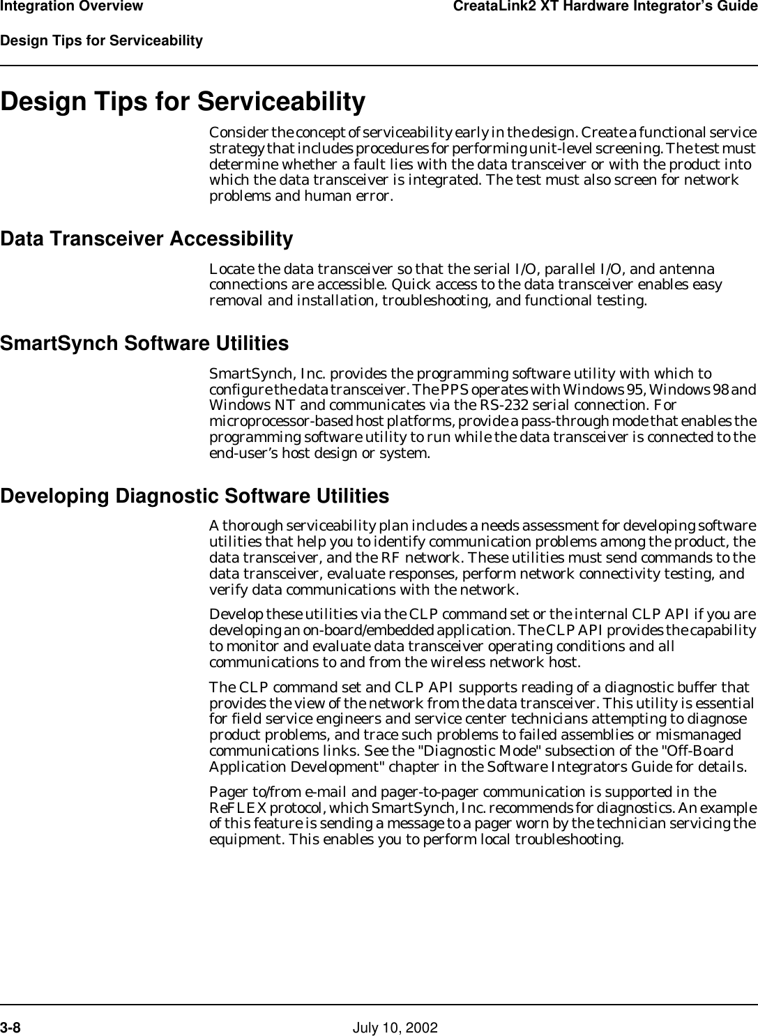

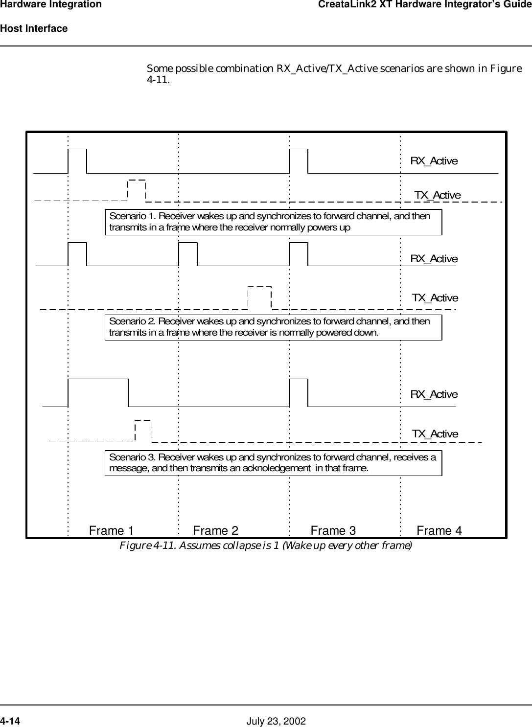


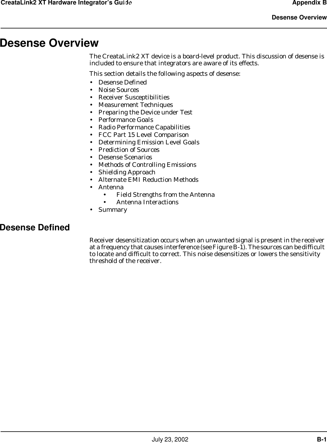
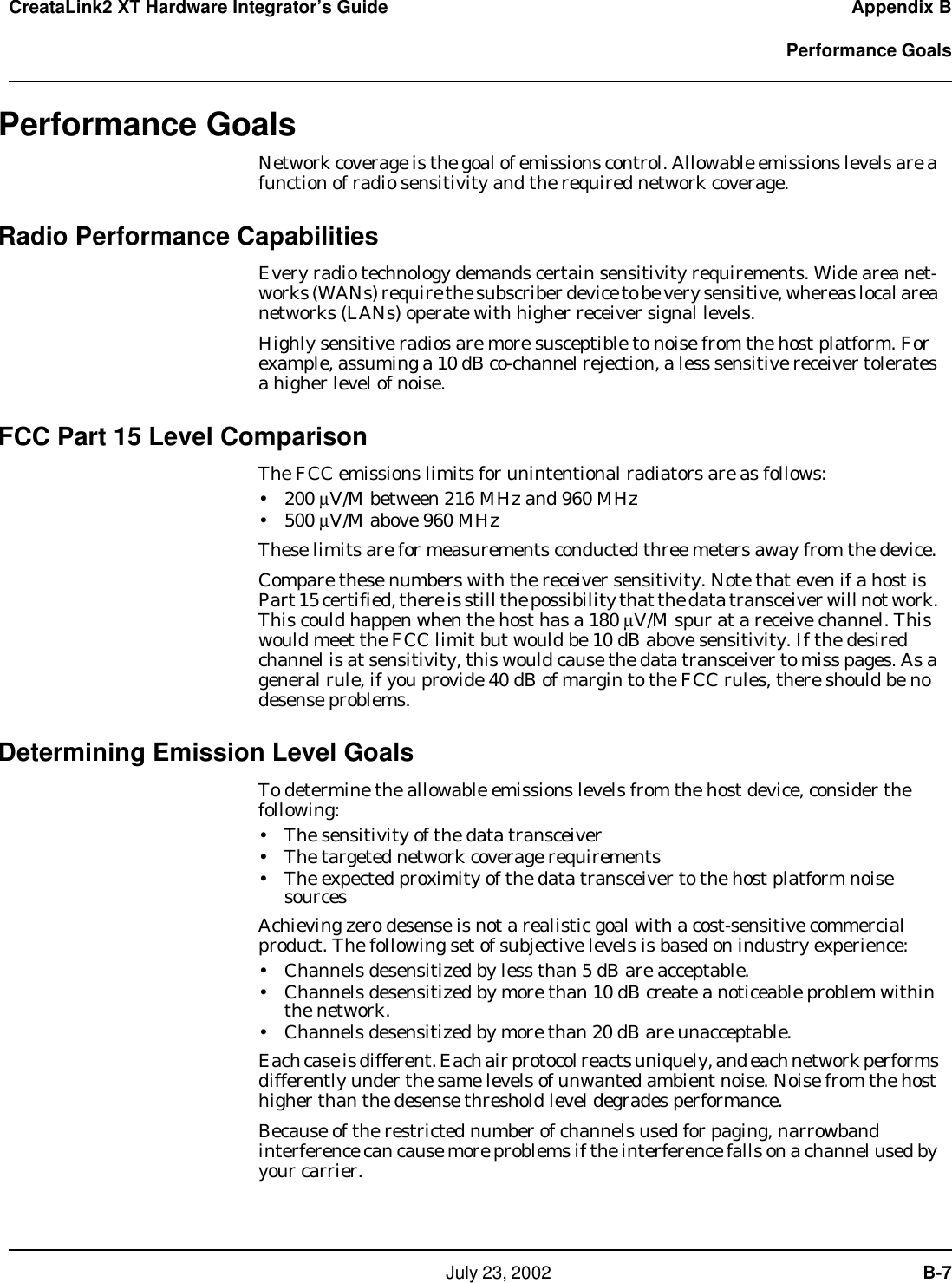
![B-2 July 23, 2002 Appendix B CreataLink2 XT Hardware Integrator’s Guide Desense OverviewThe radio cannot differentiate between wanted and unwanted signals. In frequency- modulated systems, the radio captures the strongest signal that the receiver detects. If both a wanted and an unwanted signal are present, and there is no significant difference in level, the unwanted signal can overtake the receiver, and block the wanted signal.Reliable reception occurs when you maintain a safety margin via co-channel rejection. A typical co-channel rejection is 10 dB. That is, an interference signal greater than 10 dB below the wanted signal would have little impact on the data receiver data recovery.Calculate the level of interference that creates desensitization as follows:Desense Threshold = Radio receiver sensitivity [dBm] - Co-channel rejection [dB] + Antenna Factor [dB]The antenna factor is the ability of the antenna to convert free space electromagnetic wave energy to power at the characteristic input impedance of the receiver. Any interference above this level can create desense, which reduces the radio sensitivity for reception. Every 1 dB above the threshold level creates 1 dB of desense.A worst case scenario is a noise source at the same frequency as the channel center frequency. This noise source is for any signal that falls within the channel band-width of the radio receiver. Desense also occurs at IF down-conversion frequencies. For the CreataLink2 data transceiver, the receiver bandwidth is 10 kHz; the first IF is at 45.1 MHz, and the second IF is at 455 kHz. Oscillator frequencies are 16.8 MHz, 45.555 MHz, and at the channel frequency minus 45.1 MHz.990005Figure B-1. Wanted and Unwanted Signal LevelsAmplitudeFc = Radio Receiver Channel FrequencyFrequencyFcWanted Signal LevelUnwanted Signal Level](https://usermanual.wiki/Itron/0001/User-Guide-262278-Page-112.png)
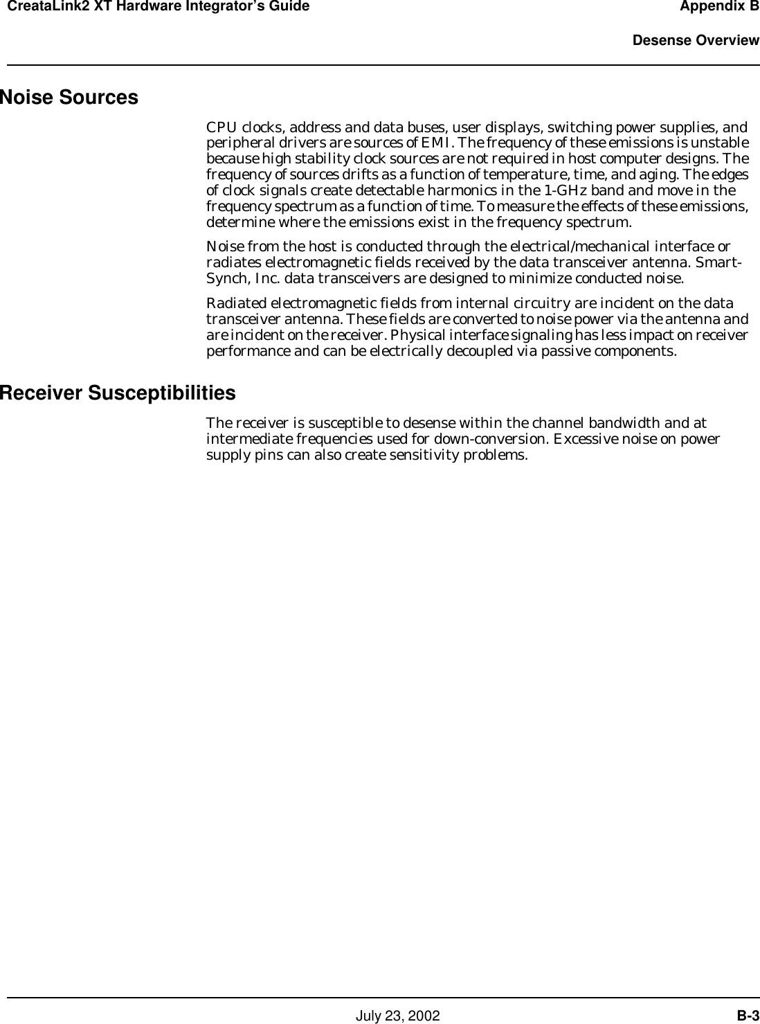
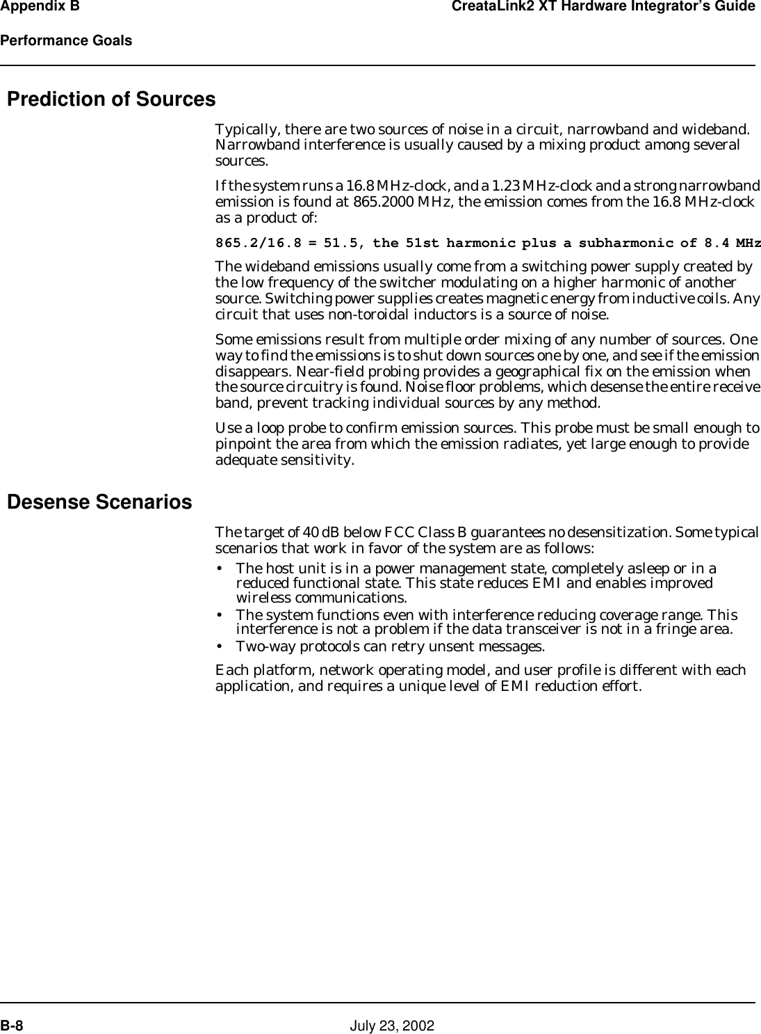
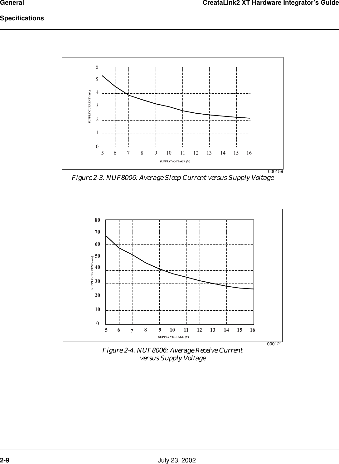
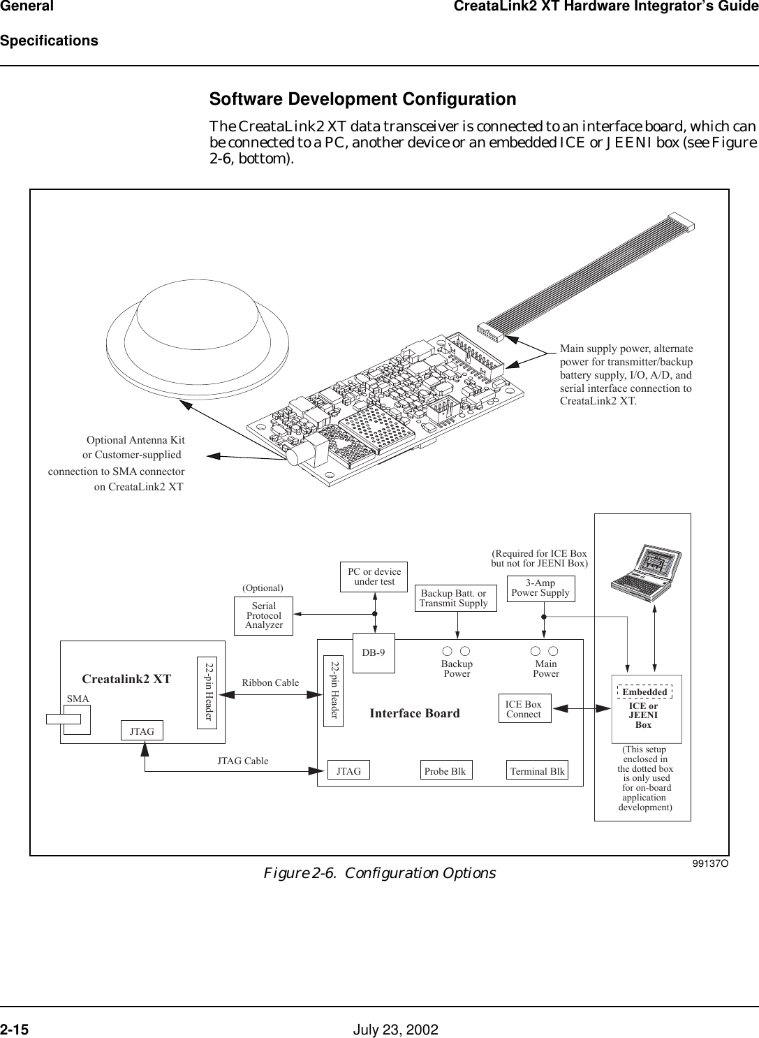
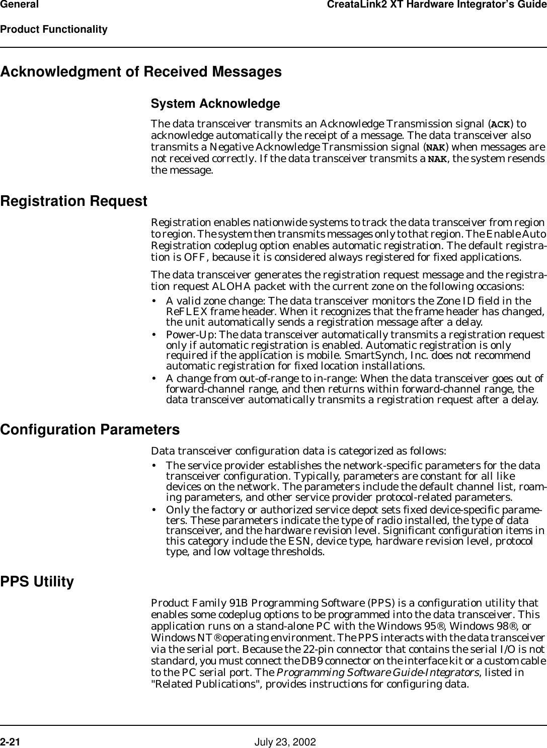
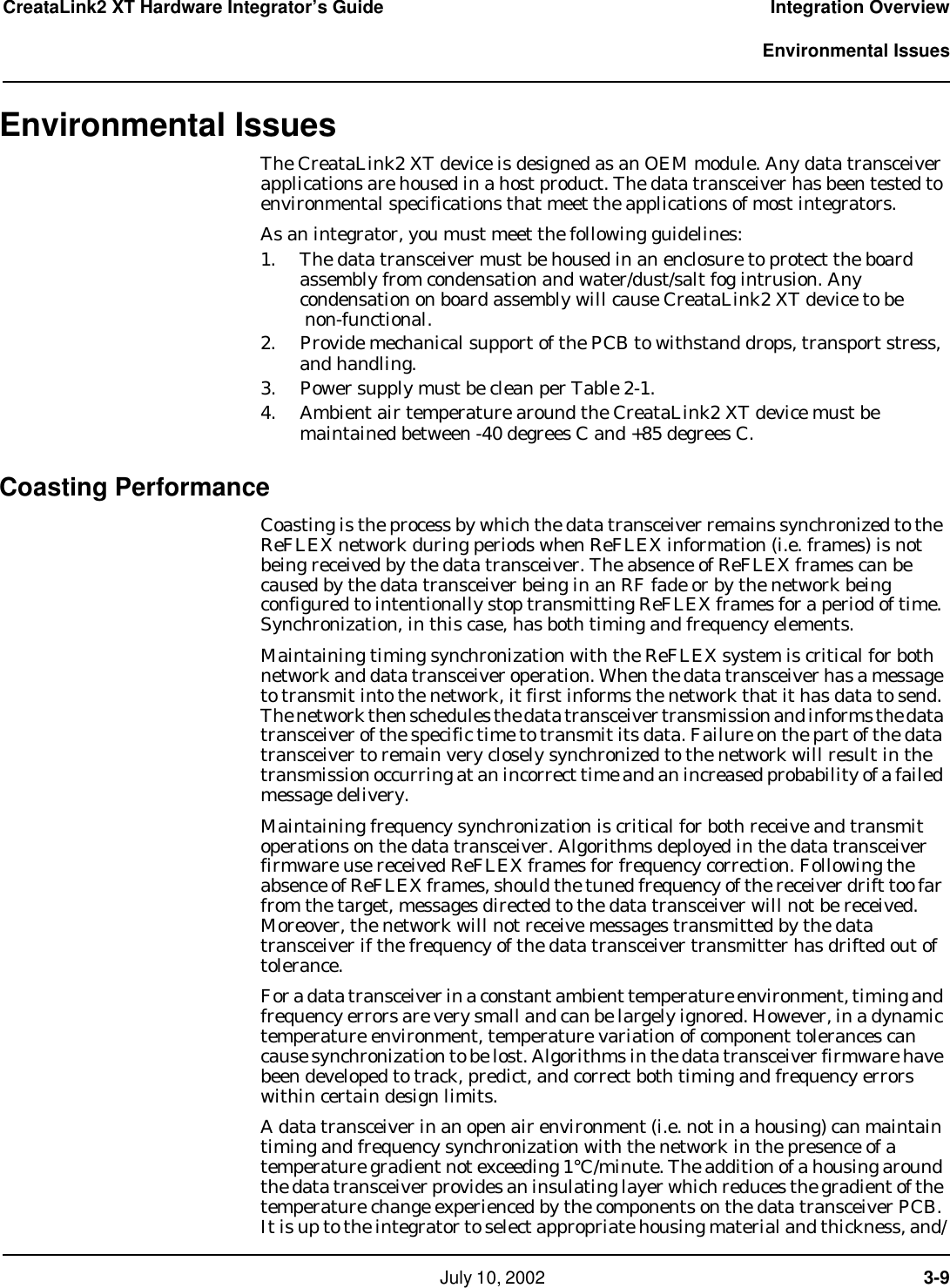
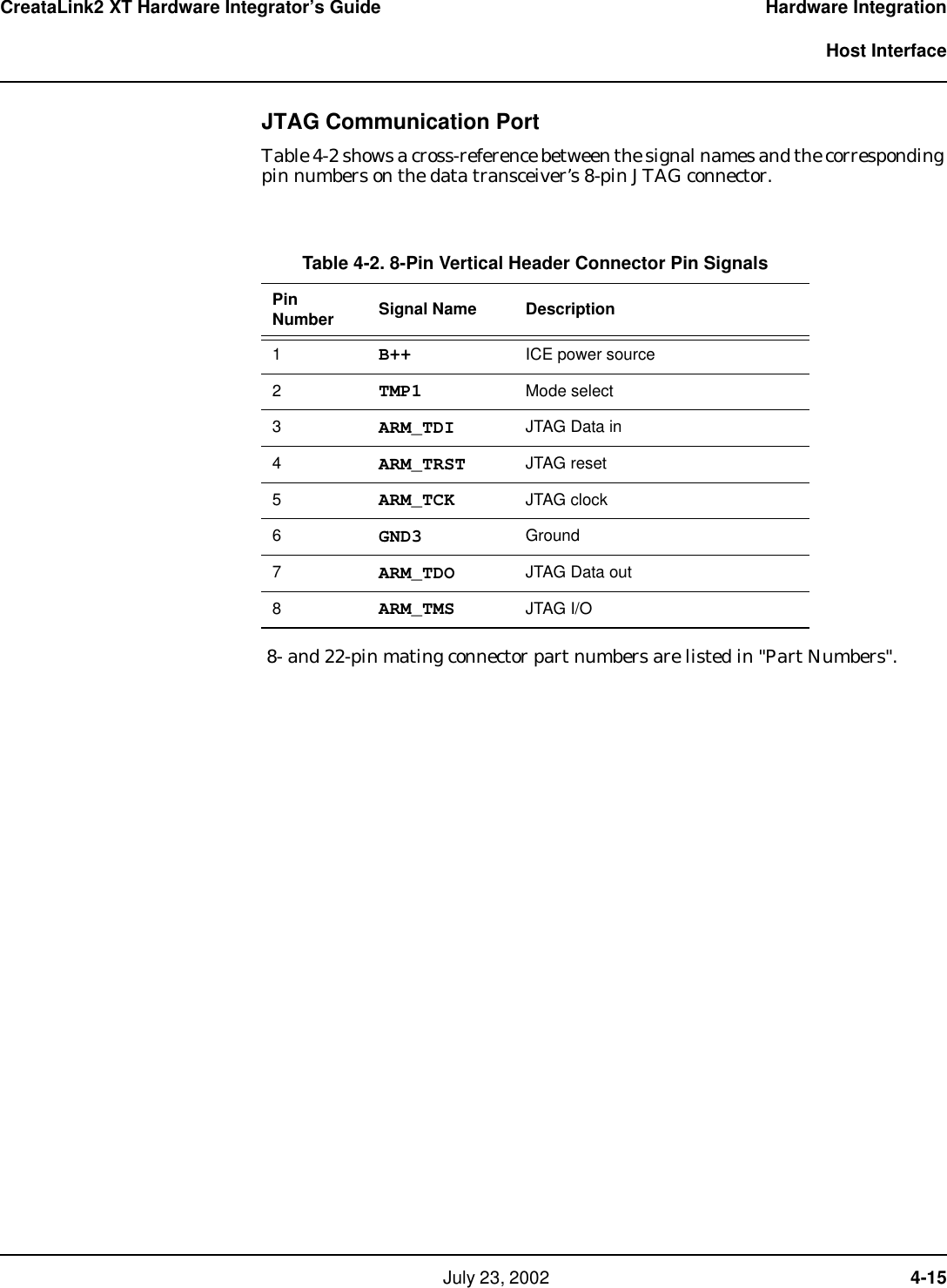
![B-4 July 23, 2002 Appendix B CreataLink2 XT Hardware Integrator’s Guide Desense Measurement TechniquesDesense Measurement TechniquesTo measure desense indirectly, record the emission level from the host and then calculate the effect on the data transceiver. To measure desense directly, use packet error rate testing off the air. The direct method is similar to a system test. The test should be non-intrusive, with no peripheral test cables connected to the unit under test. Cables have a significant effect on receiver sensitivity results.Indirect testing is FCC Part 15 EMI testing. Some assumptions are made to extrapolate the results and convert them to desense figures. The best way to measure desense is to use a spectrum analyzer to measure the signal the receive port detects (see Figure B-2).Connect the product antenna to a spectrum analyzer that has an input impedance of 50 ohms. If the antenna is not available, use a portable dipole antenna as a measurement antenna. This measurement method determines the amount of RF energy that the host device emits. The measurement does not account for any noise that is transmitted through a conductive pathway.With the input impedance of the analyzer and the antenna the same as the radio receiver, the analyzer measures the actual receiver noise. Use the following calculation to determine the level at which desense occurs:Desense Threshold = Radio Receiver sensitivity [dBm] - Co-channel rejection [dB] + Antenna Factor [dB]Depending on its frequency, any noise source above this level can create desense.The indirect method is less effective than the direct method because it does not account for the characteristics of the data protocol. The bandwidth of the noise source is important. If the source is narrowband, it may cause more problems than a wideband source. There are only a limited number of channels available. Therefore, a noise source that desenses a single channel can cause the data transceiver to fail. 805SRH-26Figure B-2. Spectrum Analyzer SetupCoaxial Connection to Measurement AntennaMeasurement AntennaUnit Under Test Spectrum Analyzer805SRH-26](https://usermanual.wiki/Itron/0001/User-Guide-262278-Page-114.png)