Japan Radio CMN851A Wireless LAN Module User Manual CMN 851A Manual 130617
Japan Radio Co Ltd. Wireless LAN Module CMN 851A Manual 130617
(Short term Confidential) Users Manual

Date of issue:11 APL 2013
Document Number WN-AG0038A
Users Manual
Product name: Wireless LAN Module
Type:
::
:CMN-851A
Rev.
..
.1
11
1.
..
.0
00
00
00
0
Japan Radio Co., Ltd.
Mobile Communication Group

i
History
Rev.
Date Change Record
1.00 2013.04.11 First Edition

Table of contents
1. GENERAL .................................................................................................................................. 1
2. SPECIFICATIONS FOR WIRELESS LAN ................................................................................. 1
2.1 Environment .......................................................................................................................... 1
2.2 Power .................................................................................................................................... 1
2.3 Radio specification ................................................................................................................ 1
2.4 Radio specifications .............................................................................................................. 2
2.5 Block diagram ....................................................................................................................... 6
2.6 Host interface ........................................................................................................................ 7
2.7 Environmental load ............................................................................................................. 10
2.8 MTBF .................................................................................................................................. 10
3. RELIABILITY TEST .................................................................................................................. 11
4. PACKING .................................................................................................................................. 11
5. ASSURANCE ........................................................................................................................... 11
6. STRUCTURE ........................................................................................................................... 11
7. LOCATION OF MANUFACTURE ............................................................................................. 11
8. NOTE ........................................................................................................................................ 12
1
1. General
This equipment is Wireless LAN Module for IEEE802.11 a/b/g/n (2.4GHz band/5GHz band)
with PCI-Express mini-card interface.
2. Specifications for Wireless LAN
2.1 Environment
(1) Temperature
Operation 0~+50℃(Ta:Ambient Temperature)
0~+65℃(Tc:Case Surface Temperature )
Storage -40~+85℃(Ta:Ambient Temperature)
(2) Humidity
Operation 20~95%RH(no condensation)
Storage 20~95%RH(no condensation)
2.2 Power
(1) Input Supply from the host interface connector
(2) Operation voltage DC3.3V ±5%
(3) Maximum voltage +3.6V
(4) Ripple Less than 100mVp-p
(5) Consumption current See Table 1
Table 1.Consumption Current (Source voltage is 3.3V)
Condition TYP MAX
2.4GHz Band (Tx) 440mA 740mA
5GHz Band(Tx) 630mA 930mA
2.4GHz Band (Rx) 200mA 350mA
5GHz Band (Rx) 230mA 360mA
2.3 Radio specification
(1) Standard ARIB STD-T71/T66, IEEE802.11a/b/g/n/e/h
11e(QoS) and 11h(DFS)are operated by driver software.
(2) Frequency
20MHz System
2.4GHz band(ISM) 2412~2472MHz,5MHz step 13ch
5.2/5.3GHz band 5180~5320MHz,20MHz step 8ch
5.6GHz band 5500~5700MHz,20MHz step 11ch
5.8GHz band 5745~5825MHz,20MHz step 5ch
40MHz System
2.4GHz band(ISM) 2422~2462MHz,5MHz step 9ch
5.2/5.3GHz band 5190~5310MHz,40MHz step 4ch
5.6GHz band 5510~5670MHz,40MHz step 5ch
5.8GHz band 5755MHz,5795MHz,40MHz step 2ch
(Note)
Available frequency is regulated by law in each country.
5.2GHz band and 5.3GHz band are for indoor use only.
(3) Mode Infrastructure / Ad-hoc(not Ad-hoc operation in the DFS band.)
(4) RF connector 20441-001E-01(IPEX, Hirose U.FL-R) 2 ports
Nominal Impedance 50ohm (Recommended ANT VSWR : <= 2)

2
(5) Modulation 2.4GHz band: OFDM, DSSS
5GHz band: OFDM
(6) MIMO 2x2,2 stream
(7) Transmit rate IEEE802.11b(DSSS/CCK) 1~11Mbps
IEEE802.11a/g(OFDM) 6~54Mbps
IEEE802.11n(OFDM,2x2MIMO) 6.5~300Mbps
(8) Functions Encryptions
Power save function and etc are operated by driver software.
(9) Security IEEE802.11i
Encryption method:WEP/TKIP/AES
2.4 Radio specifications
(1) Transmit power
2.4GHzband
Table 2.2.4GHz band
Mode Rate Tx Power allowable deviation
IEEE802.11b All rate
1~11Mbps
3mW/MHz
(14.8dBm)
+20%,-80%
(+0.8dB, -7dB)
IEEE802.11g All rate
6~54Mbps
3mW/MHz
(17.1dBm)
+20%,-80%
(+0.8dB, -7dB)
IEEE802.11n HT20
MCS8~14 3mW/MHz
(17.3dBm) +20%,-80%
(+0.8dB, -7dB)
MCS15 1.4mW/MHz
(14.0dBm)
IEEE802.11n HT40
MCS8~14 1.5mW/MHz
(17.3dBm) +20%,-80%
(+0.8dB, -7dB)
MCS15 0.7mW/MHz
(14.0dBm)
5.2/5.3GHz band
Table3.5.2/5.3GHz band
Mode Rate Tx power allowable deviation
IEEE802.11a
6~48Mbps 3mW/MHz
(17.1dBm) +20%,-80%
(+0.8dB, -7dB)
54Mbps 1.4mW/MHz
(13.8dBm)
IEEE802.11n HT20
MCS8~13 3mW/MHz
(17.3dBm) +20%,-80%
(+0.8dB, -7dB)
MCS14~15 1.4mW/MHz
(14.0dBm)
IEEE802.11n HT40
MCS8~13 1.5mW/MHz
(17.3dBm) +20%,-80%
(+0.8dB, -7dB)
MCS14~15 0.7mW/MHz
(14.0dBm)

3
5.6GHz band
Table 4.5.6GHz band
Mode Rate Tx power allowable deviation
IEEE802.11a
6~48Mbps 1.4mW/MHz
(13.8dBm) +50%,-50%
(+1.8dB, -3dB)
54Mbps 0.6mW/MHz
(10.1dBm)
IEEE802.11n HT20
MCS8~13 1.4mW/MHz
(14.0dBm) +50%,-50%
(+1.8dB, -3dB)
MCS14~15 0.6mW/MHz
(10.3dBm)
IEEE802.11n HT40
MCS8~13 0.7mW/MHz
(14.0dBm) +50%,-50%
(+1.8dB, -3dB)
MCS14~15 0.3mW/MHz
(10.3dBm)
5.8GHz band(TBD)
Table 5.5.8GHz band
Mode Rate Tx power allowable deviation
IEEE802.11a
6~48Mbps 2.0mW/MHz
(15.2dBm) +20%,-80%
(+0.8dB, -7dB)
54Mbps 1.0mW/MHz
(12.2dBm)
IEEE802.11n HT20
MCS8~13 2.0mW/MHz
(15.5dBm) +20%,-80%
(+0.8dB, -7dB)
MCS14~15 1.0mW/MHz
(12.5dBm)
IEEE802.11n HT40
MCS8~13 1.0mW/MHz
(15.5dBm) +20%,-80%
(+0.8dB, -7dB)
MCS14~15 0.5mW/MHz
(12.5dBm)
(2) Occupied band width 20MHz system
2.4GHz band Less than 26MHz
5.2/5.3GHz band Less than 19MHz
5.6//5.8GHz band Less than 19.7MHz
40MHz system
2.4GHz band Less than 38MHz
5.2/5.3/5.6/5.8GHz band Less than 38MHz
(3) Frequency accuracy 2.4GHz band ±50ppm
5.2/5.3/5.6/5.8GHz band ±20ppm
4
(4) Receiver sensitivity
Table 6.2.4GHz band
System Band
width
MCS
index
Data Rate Sensitivity [dBm]
802.11b
(2.4GHz band)
1Mbit/s Less than -80
2Mbit/s Less than -75
802.11g
(2.4GHz band)
20MHz
6Mbit/s Less than -82
9Mbit/s Less than -81
12Mbit/s Less than -79
18Mbit/s Less than -77
24Mbit/s Less than -74
36Mbit/s Less than -70
48Mbit/s Less than -66
54Mbit/s Less than -65
802.11n
(2.4GHz band)
20MHz
0 8 Less than -82
1 9 Less than -79
2 10
Less than -77
3 11 Less than -74
4 12
Less than -70
5 13
Less than -66
6 14
Less than -65
7 15
Less than -64
40MHz
0 8 Less than -79
1 9 Less than -76
2 10
Less than -74
3 11 Less than -71
4 12
Less than -67
5 13
Less than -63
6 14
Less than -62
7 15
Less than -61
5
Table 7.5GHz band
System Band
width
MCS
index
Data Rate Sensitivity [dBm]
802.11a
(5GHz band) 20MHz
6Mbit/s Less than -82
9Mbit/s Less than -81
12Mbit/s Less than -79
18Mbit/s Less than -77
24Mbit/s Less than -74
36Mbit/s Less than -70
48Mbit/s Less than -66
54Mbit/s Less than -65
802.11n
(5GHz band)
20MHz
0 8 Less than -82
1 9 Less than -79
2 10
Less than -77
3 11
Less than -74
4 12
Less than -70
5 13
Less than -66
6 14
Less than -65
7 15
Less than -64
40MHz
0 8 Less than -79
1 9 Less than -76
2 10
Less than -74
3 11
Less than -71
4 12
Less than -67
5 13
Less than -63
6 14
Less than -62
7 15
Less than -61
6
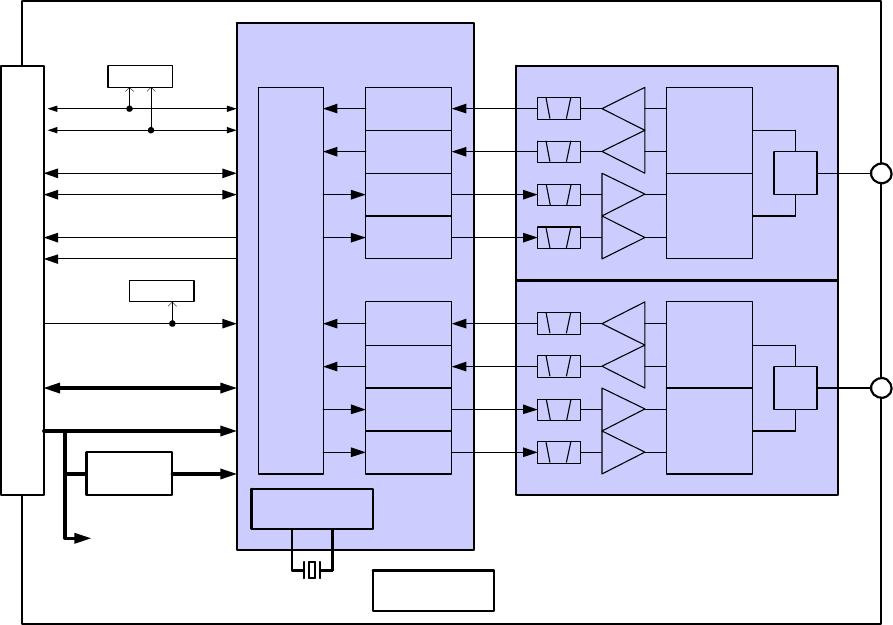
2.5 Block diagram
PLL / VCO
PCIe
MAC
/BB
2G-RX1
5G-RX1
2G-TX1
5G-TX1
RX
Diplexer
SW
TX
Diplexer
40MHz
FEM
MAC/BB/RF
EEPROM
3.3V
DC/DC
1.2V
3.3V
PCIe Card edge
ANT2
WLAN-IC
GPIO0
COEX1
Pull up
GPIO1
GPIO5
GPIO6
WAKE#
CLKREQ#
PET, PER, REFCLK
2G-RX2
5G-RX2
2G-TX2
5G-TX2
COEX2
W_DISABLE#
LED_WLAN#
PERST#
Pull up
RX
Diplexer
SW
TX
Diplexer
FEM
ANT1
Fig 1
.
Block diagram

7
2.6
Host interface
(1)
Interface PCI-express mini-card Rev1.1 base
(2)
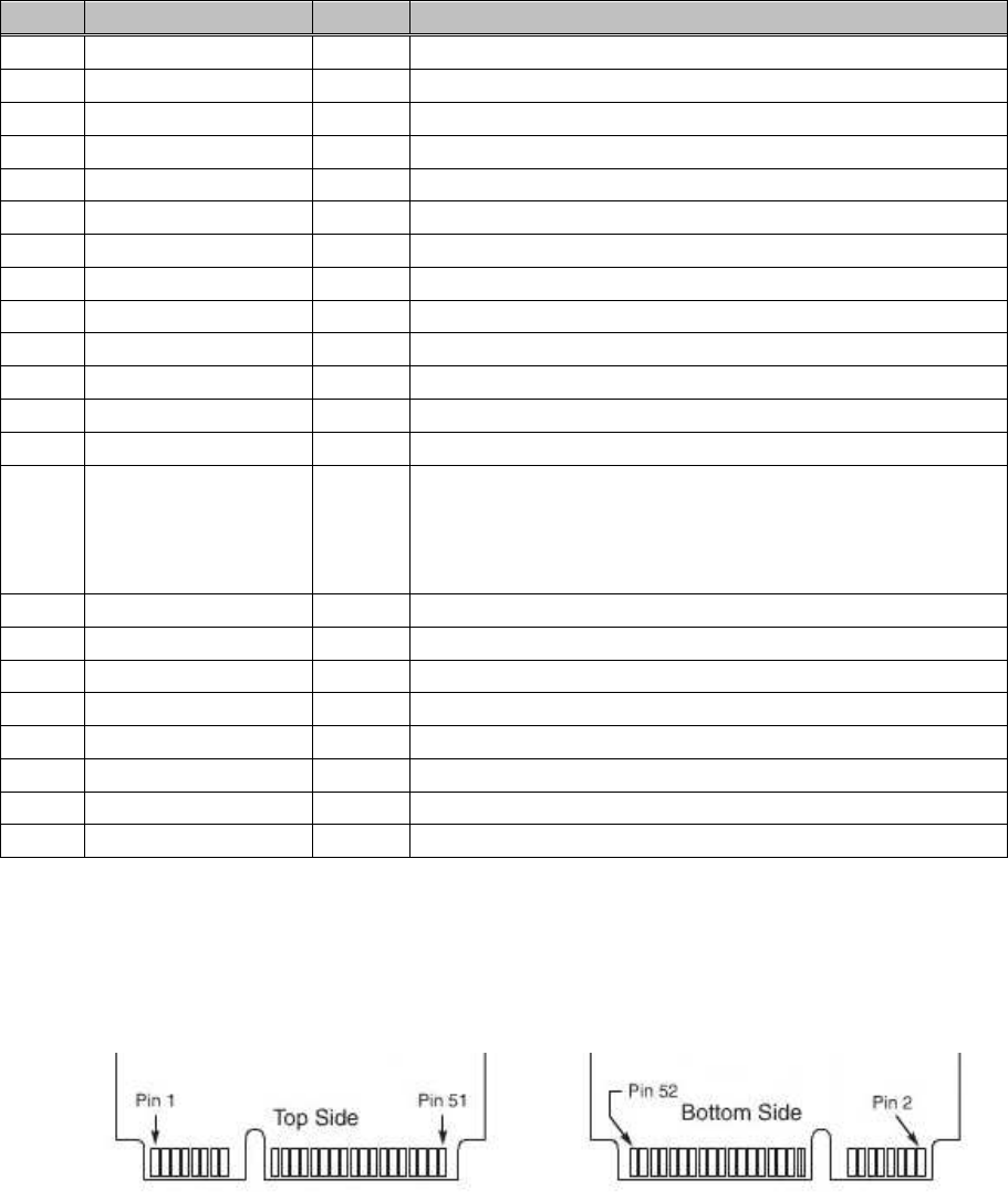
PIN assign
Table 9
.
Host interface
Pin Name Type explanation
1
#WAKE OD PCIE Request to service a function-initiated wake event
Open drain(Drive current:24mA max)
2
3.3Vaux 3.3V input
3
COEX1 I/O
Connected to AR9280-GPIO 5pin
Drive current:24mA max (Current is defined driver software)
250k ohm pull down (settable)
4
GND Ground
5
COEX2 I/O
Connected to AR9280-GPIO 6pin
Drive current:24mA max (Current is defined driver software)
250k ohm pull down (settable)
6
1.5V NC
7
CLKREQ# OD PCIE Reference clock request。
Open drain(Drive current:24mA max)
8
UIM PWR NC
9
GND Ground
10
UIM_DATA NC
11
REFCLK- I PCIE Differential reference clock(100MHz)
12
UIM_CLK NC
13
REFCLK+ I PCIE Differential reference clock(100MHz)
14
UIM_RESET NC
15
GND Ground
16
UIM_VPP NC
17
Reserved (UIM_C8)
NC
18
GND Ground
19
Reserved (UIM_C4)
NC
20
W_DISABLE# IH/OH
Connected to AR9280-GPIO 0pin
10k ohm pull up
Drive current:24mA max (Current is defined driver software)
21
GND Ground
22
PERST# IH PCIE reset 100k ohm pull up
23
PERn0 O PCIE Differential transmit
24
3.3Vaux 3.3V input
25
PERp0 O PCIE Differential transmit
26
GND Ground
27
GND Ground
28
+1.5V NC
29
GND Ground
30
SMB_CLK NC
8
※
Type: I=input, O=Output, OD=Open drain, H=Pull up
Fig 2
.
Pin allocation
Pin Name Type explanation
31
PETn0 I PCIE Differential receive
32
SMB_DATA NC
33
PETp0 I PCIE Differential receive
34
GND Ground
35
GND Ground
36
USB_D- NC
37
GND Ground
38
USB_D+ NC
39
3.3Vaux 3.3V input
40
GND Ground
41
3.3Vaux 3.3V input
42
LED_WWAN# NC
43
GND Ground
44
LED_WLAN# IH/OH
Connected AR9280-GPIO 1pin
10k ohm pull up
Drive current :24mA max (Current is defined driver
software)
45
Reserved NC
46
LED_WPAN# NC
47
Reserved NC
48
+1.5V NC
49
Reserved NC
50
GND Ground
51
Reserved NC
52
3.3Vaux 3.3V input
9
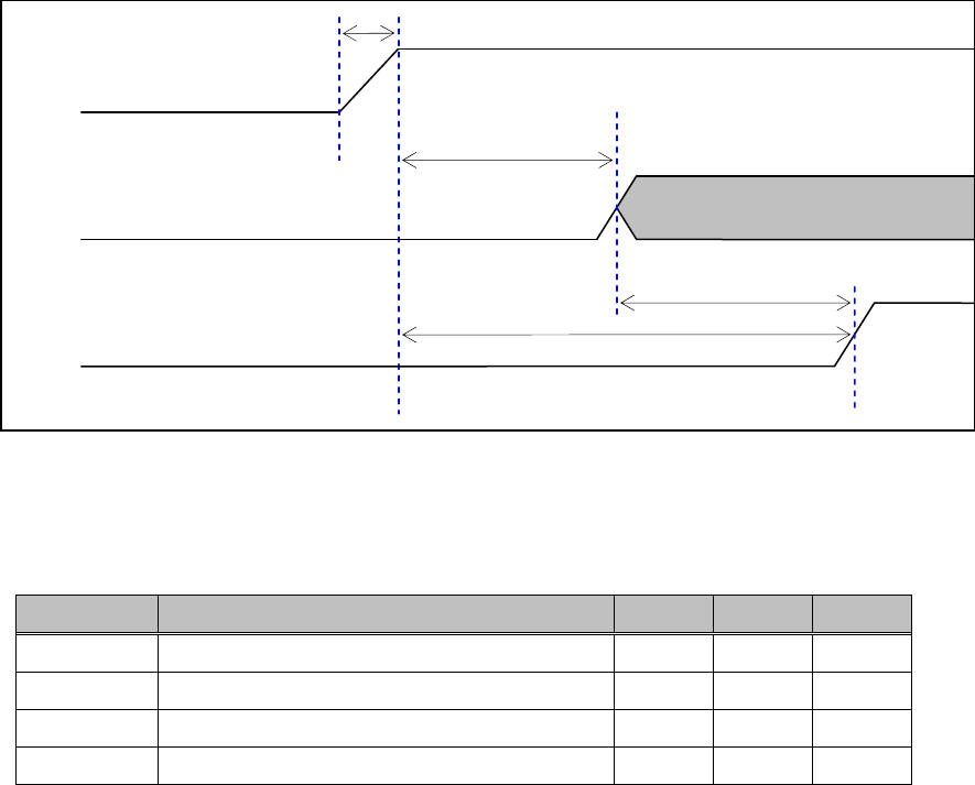
(3)
Start up sequence
Please comply with the following timing.
Fig 3
.
Start up sequence
Table 10
.
Start up timing
Signal Name Min Max Unit
T
PVRAMP
Power Supply Ramp on 3.3V - 1 ms
T
PV2CLK
Power valid to REFCLK stable 100 - us
T
CLK2RST
REFCLK stable to PERST# de-asserted 100 - us
T
PV2RST
Power valid to PERST# de-asserted 10 - ms
T
PVRAMP
T
PV2CLK
T
PV2RST
3.3Vaux
Input
Input
REFCLK
PERST#
T
CLK2RST

10
2.7
Environmental load
(1)
RoHS available
2.8
MTBF
25 years
(Condition)
Temperature 0
℃
to 50
℃
Humidity 93%(40
℃
)
Vibration Frequency 10 to 200 Hz
Accelerations 29.4m/s
2
Time
:
Up and Down 4H, Back and force 2H,
Right and left 2H
Shock Peak acceleration: 500 m/s
2
Time: 11ms
Profile: half sin
Number of shock: 3 times each axis (Total 18 times)
。

11
3.
Reliability test
Contact us
4.
Packing
See packing instruction
5.
Assurance
(
1
)
Duration of guarantee
1 year
(2)Analysis method
It supports only re-test on the production line.
6.
Structure
See “Parts allocation” and “Parts list”
7.
Location of manufacture
Factory Japan Radio Co., Ltd. MITAKA plant
Place MITAKA CITY, TOKYO MET.
Country Japan
12
8.
Note
FCC/IC CAUTION
This device complies with Part 15 of FCC Rules and Industry Canada licence-exempt RSS
standard(s). Operation is subject to the following two conditions: (1) this device may not
cause interference, and (2) this device must accept any interference, including
interference that may cause undesired operation of this device.
Le présent appareil est conforme aux la partie 15 des règles de la FCC et CNR d'Industrie
Canada applicables aux appareils radio exempts de licence. L'exploitation est autorisée
aux deux conditions suivantes : (1) l'appareil ne doit pas produire de brouillage, et (2)
l'utilisateur de l'appareil doit accepter tout brouillage radioélectrique subi, même si le
brouillage est susceptible d'en compromettre le fonctionnement.
RF exposure compliance
This equipment complies with FCC/IC radiation exposure limits set forth for an
uncontrolled environment and meets the FCC radio frequency (RF) Exposure Guidelines
in Supplement C to OET65 and RSS-102 of the IC radio frequency (RF) Exposure rules.
This equipment should be installed and operated keeping the radiator at least 20cm or
more away from person’s body (excluding extremities: hands, wrists, feet and ankles).
Cet équipement est conforme aux limites d’exposition aux rayonnements énoncées pour
un environnement non contrôlé et respecte les règles les radioélectriques (RF) de la FCC
lignes directrices d'exposition dans le Supplément C à OET65 et d’exposition aux
fréquences radioélectriques (RF) CNR-102 de l’IC. Cet équipement doit être installé et
utilisé en gardant une distance de 20 cm ou plus entre le dispositif rayonnant et le corps
(à l’exception des extrémités : mains, poignets, pieds et chevilles).
Compliance with FCC requirement 15.407(c) and IC requirement RSS-210 A9.4 4
Data transmission is always initiated by software, which is the passed down through the
MAC, through the digital and analog baseband, and finally to the RF chip. Several special
packets are initiated by the MAC. These are the only ways the digital baseband portion
will turn on the RF transmitter, which it then turns off at the end of the packet. Therefore,
the transmitter will be on only while one of the aforementioned packets is being
transmitted. In other words, this device automatically discontinue transmission in case of
either absence of information to transmit or operational failure.
La transmission des données est toujours commencée par logiciel qui est les passés en
bas à travers le MAC à travers le baseband numérique et analogique, et finalement à
l'éclat RF. Plusieurs paquets spéciaux sont commencés par le MAC. Ce sont les seuls
chemins que la portion du baseband numérique allumera le transmetteur RF qu'il
désactive alors à la fin du paquet. Par conséquent, le transmetteur sera sur seulement
pendant qu'un des parquets susmentionnés est transmis. En d'autres termes, cet appareil
cesse automatiquement la transmission en cas de l'un et l'autre absence d'information
pour transmettre ou échec opérationnel.

13
FCC CAUTION
Changes or modifications not expressly approved by the party responsible for
compliance could void the user’s authority to operate the equipment.
5.15-5.25GHz band is restricted to indoor operations only.
Frequency Tolerance:
±
50 ppm (2.4GHz band),
±
20 ppm (5GHz band)
IC CAUTION
Under Industry Canada regulations, this radio transmitter may only operate using an
antenna of a type and maximum (or lesser) gain approved for the transmitter by Industry
Canada. To reduce potential radio interference to other users, the antenna type and its
gain should be so chosen that the equivalent isotropically radiated power (e.i.r.p.) is not
more than that necessary for successful communication.
Conformément à la réglementation d'Industrie Canada, le présent émetteur radio peut
fonctionner avec une antenne d'un type et d'un gain maximal (ou inférieur) approuvé pour
l'émetteur par Industrie Canada. Dans le but de réduire les risques de brouillage
radioélectrique à l'intention des autres utilisateurs, il faut choisir le type d'antenne et son
gain de sorte que la puissance isotrope rayonnée équivalente (p.i.r.e.) ne dépasse pas
l'intensité nécessaire à l'établissement d'une communication satisfaisante.
5.15-5.25GHz band is restricted to indoor operations only.
La bande 5 150-5 250 MHz est restreints à une utilisation à l’intérieur.
This product which is intended for use in Japan, is a controlled product regulated under the Japanese Foreign
Exchange and Foreign Trade Law. When you plan to export or take this product out of Japan, please obtain a
permission, as required by the Law and related regulations, from the Japanese Government.
Appendix1
11
1
A
XXX
-
YYYY

CMN-851A Parts list
Reference
Designator
Vendor Vendor Part Number Description
BAL101 Murata LDB182G4510G-120 BALUN, 2.45 GHz, 50-100 OHM
BAL102 Murata LDB182G4510G-120 BALUN, 2.45 GHz, 50-100 OHM
C101 Murata GRM033B11A103KA01D CAP, 0603, B, 0.01uF
C102 Murata GRM033B11A103KA01D CAP, 0603, B, 0.01uF
C103 Murata GRM033B11A103KA01D CAP, 0603, B, 0.01uF
C104 Murata GRM033B30J104KE18D CAP, 0603, B, 0.1uF
C105 Murata GRM188B30J475KE18D CAP, 1608, B, 4.7uF
C106 Murata GRM188B30J106ME47D CAP, 1608, B, 10uF
C107 Murata GRM188B30J475KE18D CAP, 1608, B, 4.7uF
C108 Murata GRM033B30J104KE18D CAP, 0603, B, 0.1uF
C109 Murata GRM033B30J104KE18D CAP, 0603, B, 0.1uF
C110 Murata GRM033B30J104KE18D CAP, 0603, B, 0.1uF
C111 Murata GRM033B30J104KE18D CAP, 0603, B, 0.1uF
C112 Murata GRM033B30J104KE18D CAP, 0603, B, 0.1uF
C113 Murata GRM033B11A103KA01D CAP, 0603, B, 0.01uF
C114 Murata GRM033B30J104KE18D CAP, 0603, B, 0.1uF
C115 Murata GRM033B11A103KA01D CAP, 0603, B, 0.01uF
C116 Murata GRM21BB30J226ME38L CAP, 2012, B, 22uF
C117 Murata GRM21BB30J226ME38L CAP, 2012, B, 22uF
C118 Murata GRM033B30J104KE18D CAP, 0603, B, 0.1uF
C119 Murata GRM033B30J104KE18D CAP, 0603, B, 0.1uF
C121 Murata GRM0332C1E100GD01D CAP, 0603, C0H, 10pF
C122 Murata GRM0332C1E110GD01D CAP, 0603, C0H, 11pF
C123 Murata GRM0332C1E100JD01D CAP, 0603, C0H, 10pF
C124 Murata GRM0332C1E470JD01D CAP, 0603, C0H, 47pF
C125 Murata GRM0332C1E470JD01D CAP, 0603, C0H, 47pF
C126 Murata GRM0332C1E470JD01D CAP, 0603, C0H, 47pF
C127 Murata GRM0332C1E470JD01D CAP, 0603, C0H, 47pF
C128 Murata GRM033B30J104KE18D CAP, 0603, B, 0.1uF
C129 Murata GRM0332C1E100JD01D CAP, 0603, C0H, 10pF
C130 Murata GRM033B30J104KE18D CAP, 0603, B, 0.1uF
C131 Murata GRM0332C1E100JD01D CAP, 0603, C0H, 10pF
C132 Murata GRM033B30J104KE18D CAP, 0603, B, 0.1uF
C133 Murata GRM155B30J105KE18D CAP, 1005, B, 1uF
C134 Murata GRM155B31A224KE18D CAP, 1005, B, 0.22uF
C135 Murata GRM033B30J104KE18D CAP, 0603, B, 0.1uF
C136 Murata GRM155B30J105KE18D CAP, 1005, B, 1uF
C137 Murata GRM155B31A224KE18D CAP, 1005, B, 0.22uF
C138 Murata GRM033B30J104KE18D CAP, 0603, B, 0.1uF
C139 Murata GRM033B30J104KE18D CAP, 0603, B, 0.1uF
C140 Murata GRM033B30J104KE18D CAP, 0603, B, 0.1uF
C141 Murata GRM033B30J104KE18D CAP, 0603, B, 0.1uF
Appendix2

C142 Murata GRM033B11A103KA01D CAP, 0603, B, 0.01uF
C143 Murata GRM033B30J104KE18D CAP, 0603, B, 0.1uF
C144 Murata GRM0332C1E100JD01D CAP, 0603, C0H, 10pF
C145 Murata GRM0332C1E100JD01D CAP, 0603, C0H, 10pF
C146 Murata GRM0332C1E100JD01D CAP, 0603, C0H, 10pF
C147 Murata GRM0334C1ER50WZ01D CAP, 0603, C0K, 0.5pF
C148 Murata GRM0334C1ER50WZ01D CAP, 0603, C0K, 0.5pF
C149 Murata GRM0332C1E1R0CD01D CAP, 0603, C0H, 1pF
C150 Murata GRM0333C1E2R2CD01D CAP, 0603, C0J, 2.2pF
C151 Murata GRM0333C1E2R2CD01D CAP, 0603, C0J, 2.2pF
C152 Murata GRM0332C1E470JD01D CAP, 0603, C0H, 47pF
C153 Murata GRM0333C1E3R9BD01D CAP, 0603, C0J, 3.9pF
C154 Murata GRM0334C1ER50WZ01D CAP, 0603, C0K, 0.5pF
C157 Murata GRM0332C1E100JD01D CAP, 0603, C0H, 10pF
C158 Murata GRM0332C1E100JD01D CAP, 0603, C0H, 10pF
C159 Murata GRM0332C1E100JD01D CAP, 0603, C0H, 10pF
C160 Murata GRM0334C1ER50WZ01D CAP, 0603, C0K, 0.5pF
C161 Murata GRM0334C1ER50WZ01D CAP, 0603, C0K, 0.5pF
C162 Murata GRM0332C1E1R0CD01D CAP, 0603, C0H, 1pF
C163 Murata GRM0333C1E2R2CD01D CAP, 0603, C0J, 2.2pF
C164 Murata GRM0333C1E2R2CD01D CAP, 0603, C0J, 2.2pF
C165 Murata GRM0332C1E470JD01D CAP, 0603, C0H, 47pF
C166 Murata GRM0333C1E3R9BD01D CAP, 0603, C0J, 3.9pF
C167 Murata GRM0333C1E3R9BD01D CAP, 0603, C0J, 3.9pF
C201 Murata GRM0332C1E470JD01D CAP, 0603, C0H, 47pF
C202 Murata GRM0332C1E100JD01D CAP, 0603, C0H, 10pF
C203 Murata GRM0332C1E100JD01D CAP, 0603, C0H, 10pF
C204 Murata GRM033B30J104KE18D CAP, 0603, B, 0.1uF
C205 Murata GRM188B30J475KE18D CAP, 1608, B, 4.7uF
C206 Murata GRM0332C1E100JD01D CAP, 0603, C0H, 10pF
C207 Murata GRM0332C1E470JD01D CAP, 0603, C0H, 47pF
C208 Murata GRM0332C1E100JD01D CAP, 0603, C0H, 10pF
C209 Murata GRM0332C1E100JD01D CAP, 0603, C0H, 10pF
C210 Murata GRM033B30J104KE18D CAP, 0603, B, 0.1uF
C211 Murata GRM188B30J475KE18D CAP, 1608, B, 4.7uF
C212 Murata GRM0332C1E100JD01D CAP, 0603, C0H, 10pF
IC101 Atheros AR9280-AL1A IC, 802.11a/b/g/n in BGA
IC102 ROHM BR24G32FJ-WE2 IC,Memory,Serial 32Kbit EEPROM
IC103 RICOH RP501K121B-TR REG,1A,PWM STEP-DWN DC/DC CONV
IC201 SiGe_Semiconductor SE2595L-R IC, Dual Band 802.11n Wireless LAN FEM
IC202 SiGe_Semiconductor SE2595L-R IC, Dual Band 802.11n Wireless LAN FEM
J201 I-PEX 20441-001E-01 CONNECTOR, Ultra-Miniature Coax
J202 I-PEX 20441-001E-01 CONNECTOR, Ultra-Miniature Coax
L101 Murata LQM2HPN2R2MJ0L IND, 2520, 2.2uH
L102 Murata LQP03TN4N7H00D IND, 0603, 4.7nH
L104 Murata LQP03TN1N0B00D IND, 0603, 1.0nH

L105 Murata LQP03TN4N7H00D IND, 0603, 4.7nH
L107 Murata LQP03TN1N0B00D IND, 0603, 1.0nH
PC101 Fujitsu Interconnect Technologies H-7PCWN0070A PCB, 6-LAYERS
R101 Panasonic ERJ2GE0R00X RES, 1005, 0 OHMS
R102 Panasonic ERJ1GE0R00C RES, 0603, 0 OHMS
R104 Panasonic ERJ2GE0R00X RES, 1005, 0 OHMS
R105 Panasonic ERJ2GE0R00X RES, 1005, 0 OHMS
R106 Panasonic ERJ1GE0R00C RES, 0603, 0 OHMS
R107 Panasonic ERJ1GEF1002C RES, 0603, 10K OHMS
R108 Panasonic ERJ1GEF1002C RES, 0603, 10K OHMS
R109 Panasonic ERJ1GEF10R0C RES, 0603, 10 OHMS
R110 Panasonic ERJ1GEF49R9C RES, 0603, 49.9 OHMS
R115 Panasonic ERJ1GE0R00C RES, 0603, 0 OHMS
R116 Panasonic ERJ1GE0R00C RES, 0603, 0 OHMS
R117 Panasonic ERJ1GEF6191C RES, 0603, 6.19K OHMS
R121 Panasonic ERJ1GEF51R0C RES, 0603, 51 OHMS
R122 Panasonic ERJ1GEF49R9C RES, 0603, 49.9 OHMS
R124 Panasonic ERJ1GEF51R0C RES, 0603, 51 OHMS
R125 Panasonic ERJ1GEF49R9C RES, 0603, 49.9 OHMS
R126 Panasonic ERJ1GEF1002C RES, 0603, 10K OHMS
R127 Panasonic ERJ1GEF1002C RES, 0603, 10K OHMS
R201 Panasonic ERJ1GEF1200C RES, 0603, 120 OHMS
R202 Panasonic ERJ1GEF51R0C RES, 0603, 51 OHMS
R203 Panasonic ERJ1GEF1200C RES, 0603, 120 OHMS
R204 Panasonic ERJ1GEF22R0C RES, 0603, 22 OHMS
R205 Panasonic ERJ1GEF22R0C RES, 0603, 22 OHMS
R206 Panasonic ERJ1GEF22R0C RES, 0603, 22 OHMS
R207 Panasonic ERJ1GE0R00C RES, 0603, 0 OHMS
R208 Panasonic ERJ1GEF3011C RES, 0603, 3.01K OHMS
R210 Panasonic ERJ1GEF1002C RES, 0603, 10K OHMS
R211 Panasonic ERJ1GEF1002C RES, 0603, 10K OHMS
R212 Panasonic ERJ1GEF1200C RES, 0603, 120 OHMS
R213 Panasonic ERJ1GEF51R0C RES, 0603, 51 OHMS
R214 Panasonic ERJ1GEF1200C RES, 0603, 120 OHMS
R215 Panasonic ERJ1GEF22R0C RES, 0603, 22 OHMS
R216 Panasonic ERJ1GEF22R0C RES, 0603, 22 OHMS
R217 Panasonic ERJ1GEF22R0C RES, 0603, 22 OHMS
R218 Panasonic ERJ1GE0R00C RES, 0603, 0 OHMS
R219 Panasonic ERJ1GEF3011C RES, 0603, 3.01K OHMS
R221 Panasonic ERJ1GEF1002C RES, 0603, 10K OHMS
R222 Panasonic ERJ1GEF1002C RES, 0603, 10K OHMS
X101 NDK NX3225SA XTAL, 40MHz
- Hohnan MTD301926B Upper case
- Hohnan MTD301927B Lower case
- Kasahara MPNN39625 Label