Jorjin Technologies WG1400-00 Wireless module User Manual WG1400 00 DTS D05 20151125
Jorjin Technologies Inc. Wireless module WG1400 00 DTS D05 20151125
UserManual.wiki
>
Jorjin Technologies
>
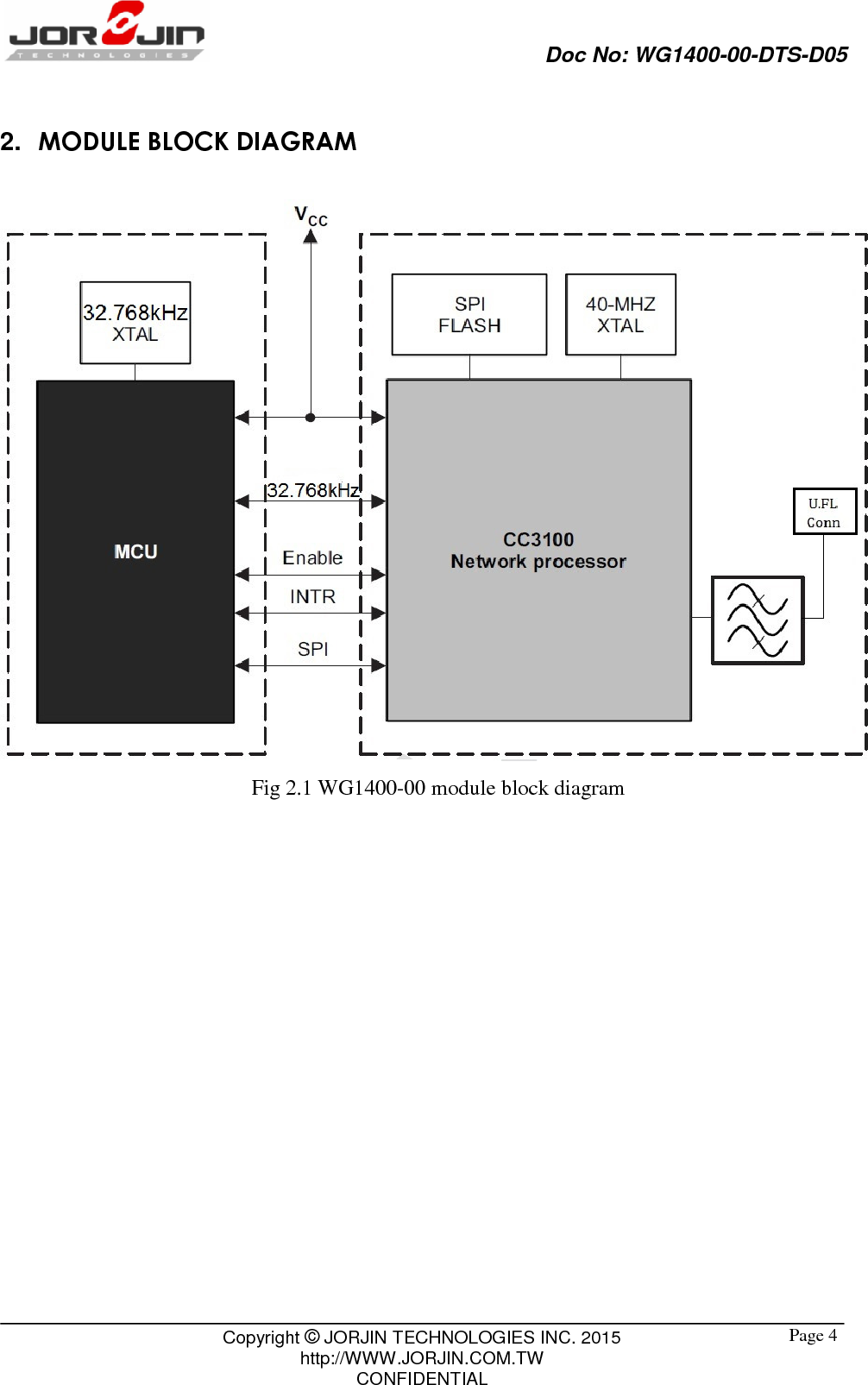
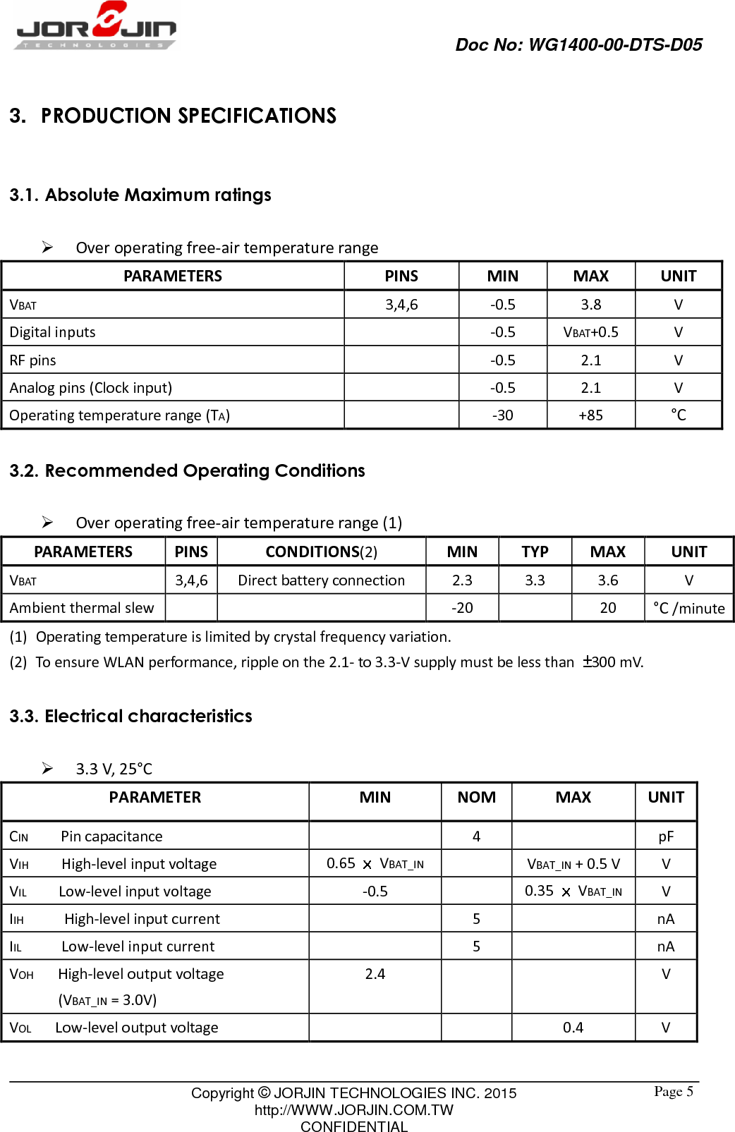
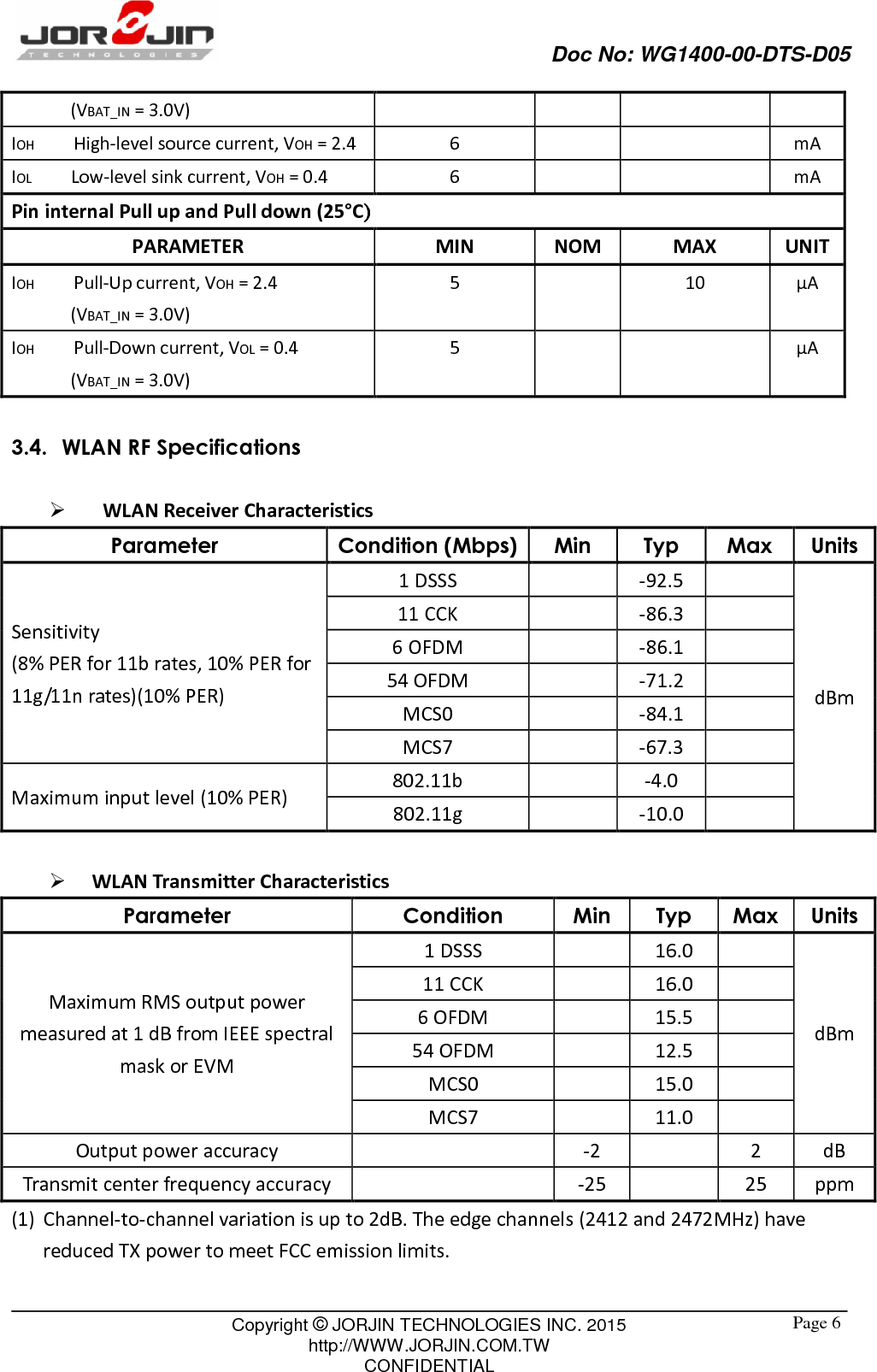
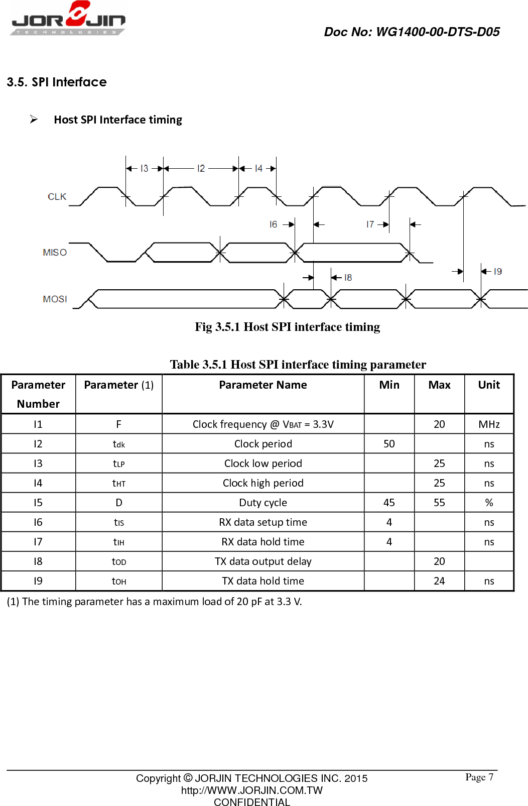
WG1400 00 User Manual
Users Manual
Navigation menu
Upload a User Manual
Namespaces
Wiki Guide
HTML
PDF
Info
Views
User Manual
Discussion / Help
Navigation