Jorjin Technologies WG7833B0 Wireless Module User Manual WG7833 B0 DTS R03 20150731
Jorjin Technologies Inc. Wireless Module WG7833 B0 DTS R03 20150731
UserManual.wiki
>
Jorjin Technologies
>
WG7833B0 User Manual
>
User Manual
Contents
1.
User Manual
2.
User Manual II
3.
User Manual III
User Manual
Navigation menu
Upload a User Manual
Namespaces
Wiki Guide
HTML
PDF
Info
Views
User Manual
Discussion / Help
Navigation
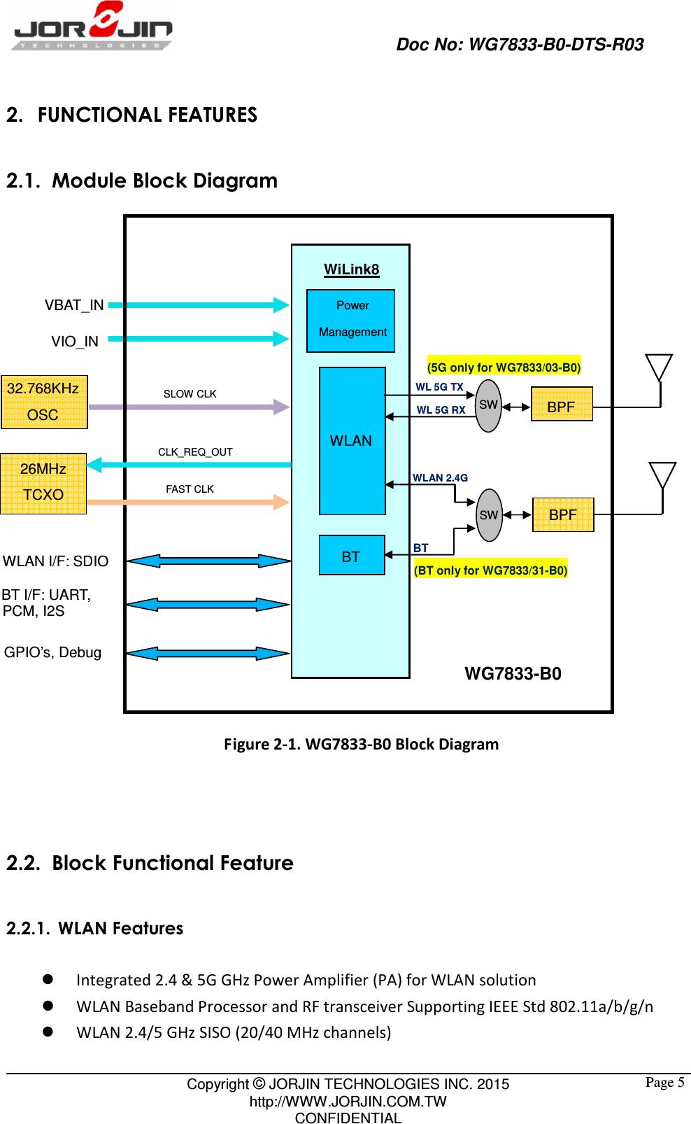
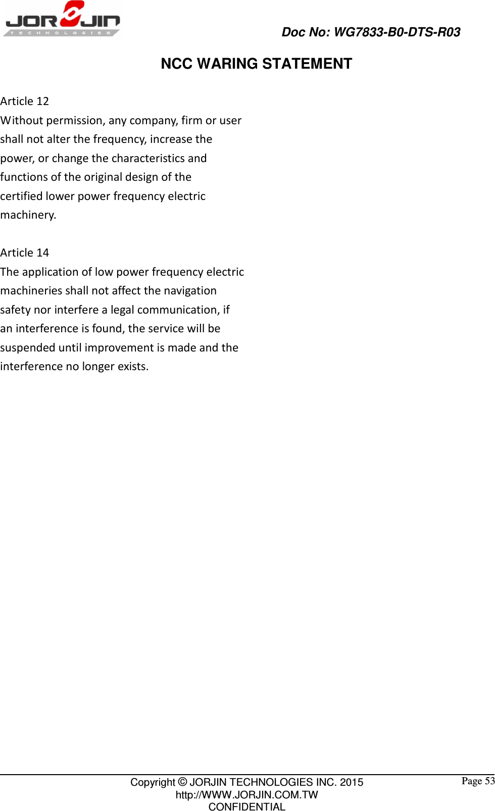
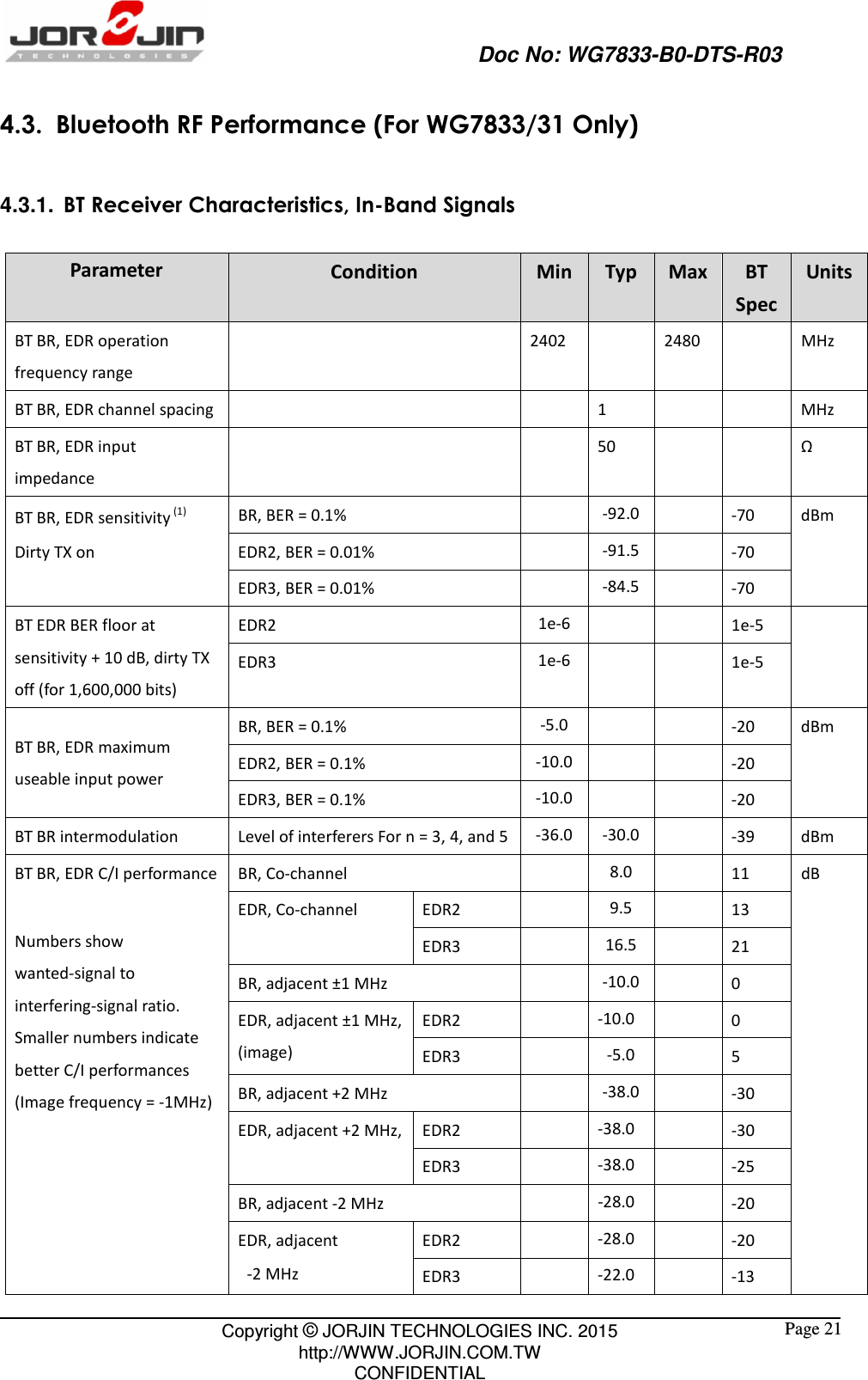
![Doc No: WG7833-B0-DTS-R03 Copyright © JORJIN TECHNOLOGIES INC. 2015 http://WWW.JORJIN.COM.TW CONFIDENTIAL Page 6 Baseband Processor IEEE Std 802.11a/b/g/n data rates and IEEE Std 802.11n data rates with 20 or 40 MHz SISO. Fully calibrated system. Production calibration not required. Medium Access Controller (MAC) Embedded ARM™ Central Processing Unit (CPU) Hardware-Based Encryption/Decryption using 64-, 128-, and 256-Bit WEP, TKIP or AES Keys, Supports requirements for Wi-Fi Protected Access (WPA and WPA2.0) and IEEE Std 802.11i [includes hardware-accelerated Advanced Encryption Standard (AES)] Designed to work with IEEE Std 802.1x IEEE Std 802.11d,e,h,i,k,r PICS compliant. New advanced co-existence scheme with BT/BLE/ANT. 2.4/5 GHz Radio Internal LNA and PA Supports: IEEE Std 802.11a, 802.11b, 802.11g and 802.11n Supports 4 bit SDIO host interface, including high speed (HS) and V3 modes. 2.2.2. Bluetooth Features Supports Bluetooth 4.0 as well as CSA2 Includes concurrent operation and built -in coexisting and prioritization handling of Bluetooth, BLE, ANT, audio processing and WLAN Dedicated Audio processor supporting on chip SBC encoding + A2DP: Assisted A2DP (A3DP) support - SBC encoding implemented internally Assisted WB-Speech (AWBS) support - modified SBC codec implemented internally 2.2.3. BLE Features Fully compliant with BT4.0 BLE dual mode standard Support for all roles and role-combinations, mandatory as well as optional Supports up to 10 BLE connections Independent buffering for LE allows having large number of multiple connections without](https://usermanual.wiki/Jorjin-Technologies/WG7833B0.User-Manual/User-Guide-2728733-Page-7.png)
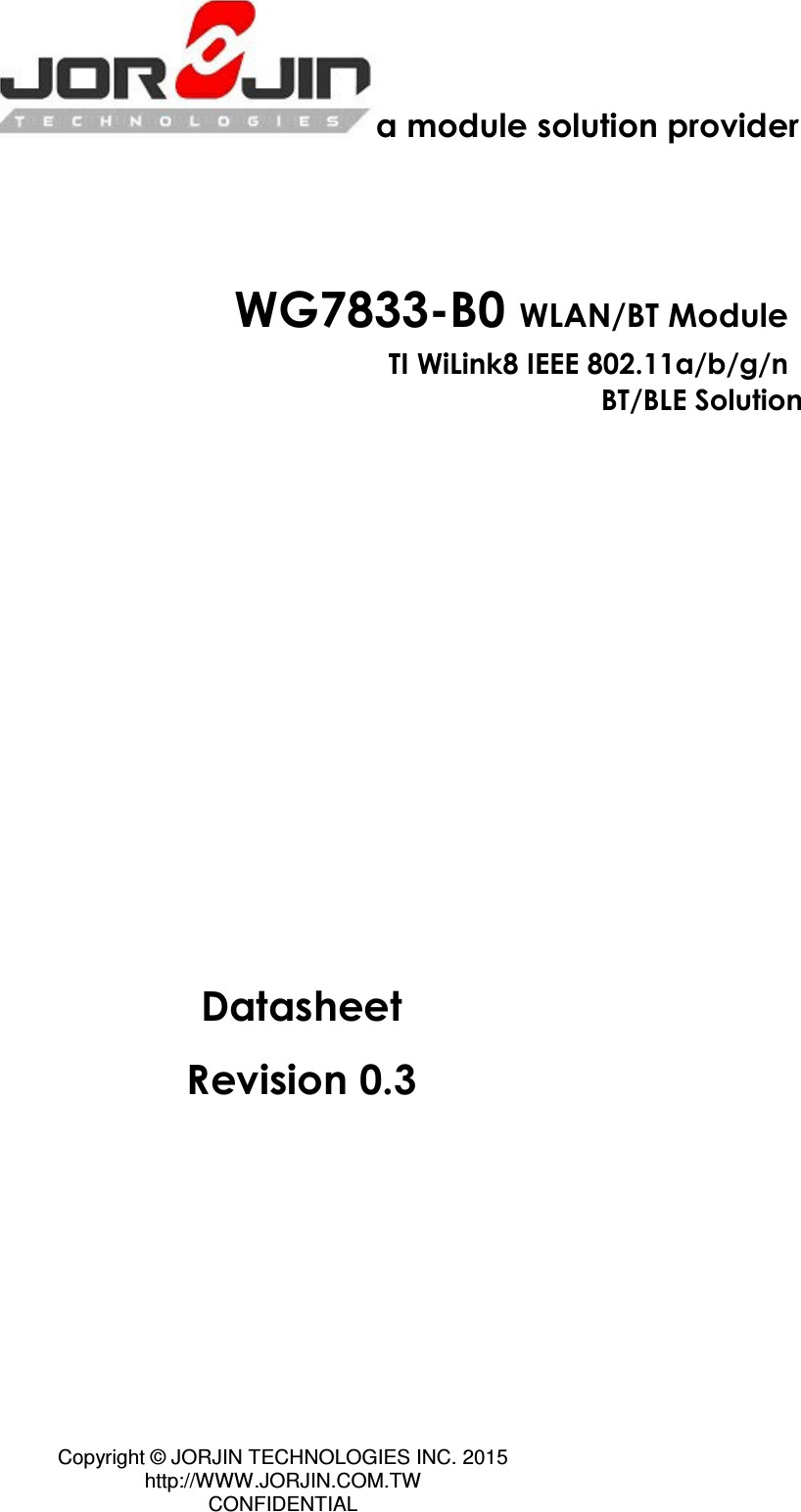
![Doc No: WG7833-B0-DTS-R03 Copyright © JORJIN TECHNOLOGIES INC. 2015 http://WWW.JORJIN.COM.TW CONFIDENTIAL Page 22 BR, adjacent ≥Ι±3Ι MHz -45.0 -40 EDR, adjacent ≥Ι±3Ι MHz EDR2 -45.0 -40 EDR3 -44.0 -33 BT BR, EDR RF return loss -10.0 dB (1) Sensitivity degradation up to -3dB may occur due to fast clock harmonics with dirty TX on. 4.3.2. BT Receiver Characteristics – General Blocking Parameter Condition Min Typ BT spec Units Blocking performance over full range, according to BT specification (1) 30-2000 MHz -6 -10 dBm 2000-2399 MHz -6 -27 2484-3000 MHz -6 -27 3-12.75 GHz -6 -10 1) Exceptions taken out of the total 24 allowed in the BT spec. 4.3.3. BT Receiver Characteristics –BR, EDR Blocking Per Band Parameter Band Min Typ Units Blocking performance for various cellular bands Hopping on. Wanted signal: -3dB from sensitivity, with modulated continuous blocking signal. BER = 0.1% for BT BR, 0.01% for BT EDR. PER = 1% 776-794 MHz (CDMA) -12 dBm 824-849 MHz (GMSK) (1) -3 824-849 MHz (EDGE) (1) -11 824-849 MHz (CDMA, QPSK) (1) -12 880-915 MHz (GMSK) -14 880-915 MHz (EDGE) -15 1710-1785 MHz (GMSK) -4 1710-1785 MHz (EDGE) -18 1850-1910 MHz (GMSK) -18 1850-1910 MHz (EDGE) -20 1850-1910 MHz (CDMA, QPSK) -20 1850-1910 MHz (WCDMA, QPSK) -16 1920-1980 MHz (WCDMA, QPSK) -17 1) Except for frequencies where [3 * F_BLOCKER] falls within the BT band (2400-2483.5 MHz)](https://usermanual.wiki/Jorjin-Technologies/WG7833B0.User-Manual/User-Guide-2728733-Page-23.png)