Jorjin Technologies WG7833B0 Wireless Module User Manual WG7833 B0 DTS R03 20150731
Jorjin Technologies Inc. Wireless Module WG7833 B0 DTS R03 20150731
Contents
- 1. User Manual
- 2. User Manual II
- 3. User Manual III
User Manual

Copyright © JORJIN TECHNOLOGIES INC. 2015
http://WWW.JORJIN.COM.TW
CONFIDENTIAL
a module solution provider
WG7833-B0
WLAN/BT Module
TI WiLink8 IEEE 802.11a/b/g/n
BT/BLE Solution
Datasheet
Revision 0.3

Doc No: WG7833-B0-DTS-R03
Copyright
©
JORJIN TECHNOLOGIES INC. 2015
http://WWW.JORJIN.COM.TW
CONFIDENTIAL
Page 1
Index
1. OVERVIEW ................................................................................................................................... 4
1.1. M
ODELS
F
UNCTIONAL
B
LOCKS
................................................................................................ 4
1.2. G
ENERAL
F
EATURES
................................................................................................................. 4
2. FUNCTIONAL FEATURES ............................................................................................................ 5
2.1. M
ODULE
B
LOCK
D
IAGRAM
..................................................................................................... 5
2.2. B
LOCK
F
UNCTIONAL
F
EATURE
.................................................................................................. 5
2.2.1. WLAN Features .......................................................................................................... 5
2.2.2. Bluetooth Features.................................................................................................... 6
2.2.3. BLE Features ................................................................................................................ 6
2.2.4. ANT Features .............................................................................................................. 7
3. MODULE OUTLINE ....................................................................................................................... 8
3.1. S
IGNAL
L
AYOUT
(T
OP
V
IEW
).................................................................................................... 8
3.2. P
IN
D
ESCRIPTION
..................................................................................................................... 9
4. MODULE SPECIFICATION ....................................................................................................... 13
4.1. G
ENERAL
M
ODULE
R
EQUIREMENTS AND
O
PERATION
............................................................ 13
4.1.1. Absolute Maximum Ratings
(1)
............................................................................. 13
4.1.2. Recommended Operating Conditions ............................................................ 14
4.1.3. External Slow Clock Input (SLOW_CLK) ............................................................ 15
4.1.4. External Fast Clock Requirements (-40 to +85°C) .......................................... 15
4.2. WLAN
RF
P
ERFORMANCE
.................................................................................................... 17
4.2.1. WLAN 2.4-GHz Receiver Characteristics .......................................................... 17
4.2.2. WLAN 2.4-GHz Transmitter Power ....................................................................... 18
4.2.4. WLAN 5-GHz Transmitter Power (For WG7833/03 Only) ............................... 20
4.3. B
LUETOOTH
RF
P
ERFORMANCE
(F
OR
WG7833/31
O
NLY
) .................................................. 21
4.3.1. BT Receiver Characteristics, In-Band Signals .................................................. 21
4.3.2. BT Receiver Characteristics – General Blocking ............................................ 22
4.3.3. BT Receiver Characteristics –BR, EDR Blocking Per Band ............................ 22
4.3.5. BT Transmitter, EDR .................................................................................................. 23
4.3.6. BT Modulation, BR ................................................................................................... 23
4.3.7. BT Modulation, EDR ................................................................................................ 24
4.3.8. BT BR, EDR Transceiver - Emissions ...................................................................... 24
4.3.9. BT BR Transceiver - Spurs........................................................................................ 25

Doc No: WG7833-B0-DTS-R03
Copyright
©
JORJIN TECHNOLOGIES INC. 2015
http://WWW.JORJIN.COM.TW
CONFIDENTIAL
Page 2
4.3.10. BT EDR Transceiver - Spurs ..................................................................................... 25
4.4. BT
LE
RF
P
ERFORMANCE
........................................................................................................... 26
4.4.1. BT LE Receiver Characteristics, In-Band Signals ....................................................... 26
4.4.3. BT LE Transmitter Characteristics .............................................................................. 27
4.4.4. BT LE Modulation Characteristics .............................................................................. 27
4.4.6. BT LE Transceiver - Spurs ........................................................................................... 28
4.5. ANT
P
ERFORMANCE
.................................................................................................................. 28
4.5.1. ANT Receiver Characteristics, In-Band Signals .......................................................... 28
4.5.2. ANT Transmitter Characteristics ................................................................................. 28
4.6. POWER
CONSUMPTION ....................................................................................................... 29
5. HOST INTERFACE TIMING CHARACTERISTICS .................................................................... 32
5.1. WLAN
SDIO
T
RANSPORT
L
AYER
................................................................................................. 32
5.2. SDIO
T
IMING
S
PECIFICATIONS
..................................................................................................... 33
5.3. HCI
UART
S
HARED
T
RANSPORT
L
AYERS FOR
A
LL
F
UNCTIONAL
B
LOCKS
(E
XCEPT
WLAN) ....................... 35
5.4. UART
T
IMING
S
PECIFICATIONS
.................................................................................................... 36
5.5. B
LUETOOTH
C
ODEC
-PCM(A
UDIO
)
T
IMING
S
PECIFICATIONS
.............................................................. 37
6. CLOCK AND POWER MANAGEMENT .................................................................................. 39
6.1. R
ESET
-P
OWER
-U
P
S
YSTEM
......................................................................................................... 39
6.2. WLAN
P
OWER
-U
P
S
EQUENCE
.................................................................................................... 39
6.3. B
LUETOOTH
/BLE/ANT
P
OWER
-U
P
S
EQUENCE
.............................................................................. 40
7. REFERENCE SCHEMATIC ......................................................................................................... 41
7.1. M
ODULE
R
EFERENCE
D
ESIGN
...................................................................................................... 41
8. DESIGN RECOMMENDATIONS .............................................................................................. 42
8.1. D
ESIGN
N
OTE ON
D
EBUG
P
ORT
.................................................................................................... 42
8.2. M
ODULE
L
AYOUT
R
ECOMMENDATIONS
......................................................................................... 42
9. PACKAGE INFORMATION ...................................................................................................... 44
9.1. M
ODULE
M
ECHANICAL
O
UTLINE
.................................................................................................. 44
9.2. O
RDERING
I
NFORMATION
........................................................................................................... 45
9.3. P
ACKAGE
M
ARKING
................................................................................................................... 46
9.4. P
ACKAGING
.............................................................................................................................. 47
10. SMT AND BAKING RECOMMENDATION ......................................................................... 49
10.1. B
AKING
R
ECOMMENDATION
............................................................................................. 49
10.2. SMT
R
ECOMMENDATION
.................................................................................................. 49

Doc No: WG7833-B0-DTS-R03
Copyright
©
JORJIN TECHNOLOGIES INC. 2015
http://WWW.JORJIN.COM.TW
CONFIDENTIAL
Page 3
11. HISTORY CHANGE ............................................................................................................... 50

Doc No: WG7833-B0-DTS-R03
Copyright
©
JORJIN TECHNOLOGIES INC. 2015
http://WWW.JORJIN.COM.TW
CONFIDENTIAL
Page 4
1. OVERVIEW
WG7833/31/03/01-B0, a WiFi, BT, BLE SiP (system in package) module, is the most demanded design
for mobile devices, Audio, Computer, PDA and embedded system applications with Wilink8 solution
from TI.
1.1. Models Functional Blocks
Model WLAN 2.4GHz WLAN 5GHz BT/BLE/ANT
WG7833-B0 V V V
1.2. General Features
WLAN, Bluetooth, BLE, ANT with Integrated RF Front-End Module (FEM), Power Amplifier (PA),
and Power Management on a Single Module
LGA106 pin package
Dimension 12.8mm(L) x 12.0mm(W) x 1.63mm(H)
Provides efficient direct connection to battery by employing several integrated switched mode
power supplies (DC2DC).
Seamless Integration with TI Sitara™ and Other Application Processors
WLAN and BT/BLE/ANT cores are software and hardware compatible with prior WL127x and
WL128x offerings, for smooth migration to device.
Shared HCI transport for BT/BLE/ANT over UART and SDIO for WLAN.
Temperature detection and compensation mechanism ensures minimal variation in RF
performance over the entire temperature range.
BT 4.0, BLE, ANT and all audio processing features work in parallel and include full coexistence
with WLAN
Operating temperature: –40°C to 85°C
Doc No: WG7833-B0-DTS-R03
Copyright
©
JORJIN TECHNOLOGIES INC. 2015
http://WWW.JORJIN.COM.TW
CONFIDENTIAL
Page 5
2. FUNCTIONAL FEATURES
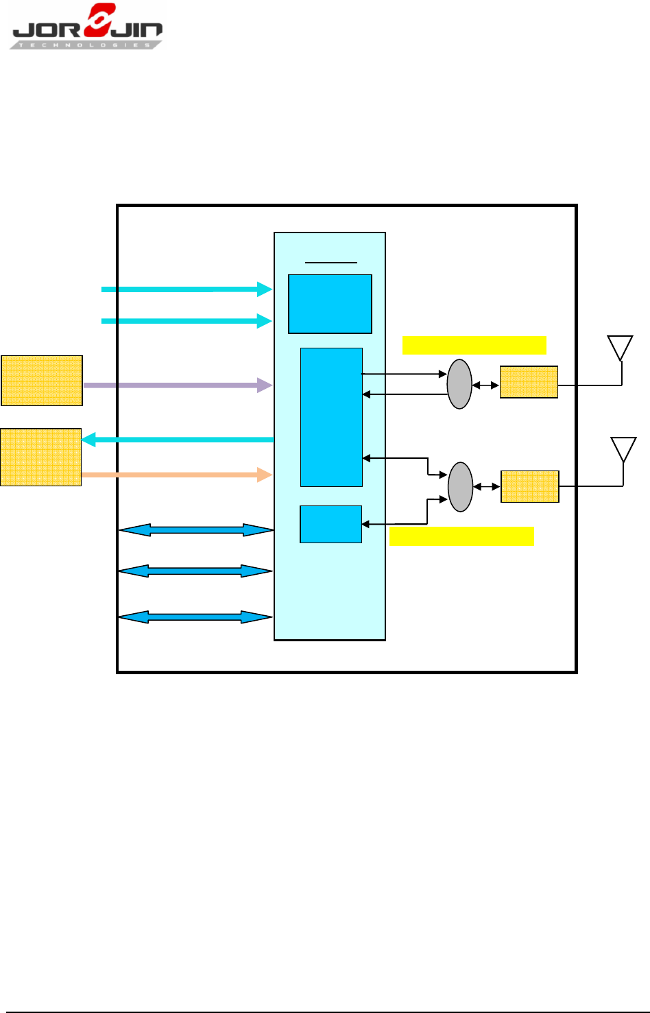
2.1. Module Block Diagram
Figure 2-1. WG7833-B0 Block Diagram
2.2. Block Functional Feature
2.2.1. WLAN Features
Integrated 2.4 & 5G GHz Power Amplifier (PA) for WLAN solution
WLAN Baseband Processor and RF transceiver Supporting IEEE Std 802.11a/b/g/n
WLAN 2.4/5 GHz SISO (20/40 MHz channels)
WLAN
BT
WiLink8
SW
WG7833-B0
VBAT_IN
VIO_IN
SLOW CLK
BT I/F: UART,
WLAN I/F: SDIO
PCM, I2S
GPIO’s, Debug
SW
WLAN 2.4G
WL 5G TX
WL 5G RX
32.768KHz
OSC
BPF
BPF
BT
(5G only for WG7833/03-B0)
(BT only for WG7833/31-B0)
26MHz
TCXO
CLK_REQ_OUT
Power
Management
FAST CLK

Doc No: WG7833-B0-DTS-R03
Copyright
©
JORJIN TECHNOLOGIES INC. 2015
http://WWW.JORJIN.COM.TW
CONFIDENTIAL
Page 6
Baseband Processor
IEEE Std 802.11a/b/g/n data rates and IEEE Std 802.11n data rates with 20 or 40
MHz SISO.
Fully calibrated system. Production calibration not required.
Medium Access Controller (MAC)
Embedded ARM™ Central Processing Unit (CPU)
Hardware-Based Encryption/Decryption using 64-, 128-, and 256-Bit WEP, TKIP
or AES Keys,
Supports requirements for Wi-Fi Protected Access (WPA and WPA2.0) and IEEE
Std 802.11i [includes hardware-accelerated Advanced Encryption Standard
(AES)]
Designed to work with IEEE Std 802.1x
IEEE Std 802.11d,e,h,i,k,r PICS compliant.
New advanced co-existence scheme with BT/BLE/ANT.
2.4/5 GHz Radio
Internal LNA and PA
Supports: IEEE Std 802.11a, 802.11b, 802.11g and 802.11n
Supports 4 bit SDIO host interface, including high speed (HS) and V3 modes.
2.2.2. Bluetooth Features
Supports Bluetooth 4.0 as well as CSA2
Includes concurrent operation and built -in coexisting and prioritization handling of
Bluetooth, BLE, ANT, audio processing and WLAN
Dedicated Audio processor supporting on chip SBC encoding + A2DP:
Assisted A2DP (A3DP) support - SBC encoding implemented internally
Assisted WB-Speech (AWBS) support - modified SBC codec implemented internally
2.2.3. BLE Features
Fully compliant with BT4.0 BLE dual mode standard
Support for all roles and role-combinations, mandatory as well as optional
Supports up to 10 BLE connections
Independent buffering for LE allows having large number of multiple connections without

Doc No: WG7833-B0-DTS-R03
Copyright
©
JORJIN TECHNOLOGIES INC. 2015
http://WWW.JORJIN.COM.TW
CONFIDENTIAL
Page 7
affecting BR/EDR performance
2.2.4. ANT Features
Fully compliant with all ANT Protocols:
ANT solution optimized for the fitness and health use-cases
Simple to complex network topologies
Supports high-resolution proximity pairing
The ANT protocol has been designed to very power-efficient, yet is flexible enough to support
various network topologies (point-to-point, star, 1-to-N, N-to-1) and data transfer modes
(broadcast, broadcast with acknowledge, mass data transfer). Each logical ANT channel can be
independently configured for 1-way or 2-way operation
Doc No: WG7833-B0-DTS-R03
Copyright
©
JORJIN TECHNOLOGIES INC. 2015
http://WWW.JORJIN.COM.TW
CONFIDENTIAL
Page 8
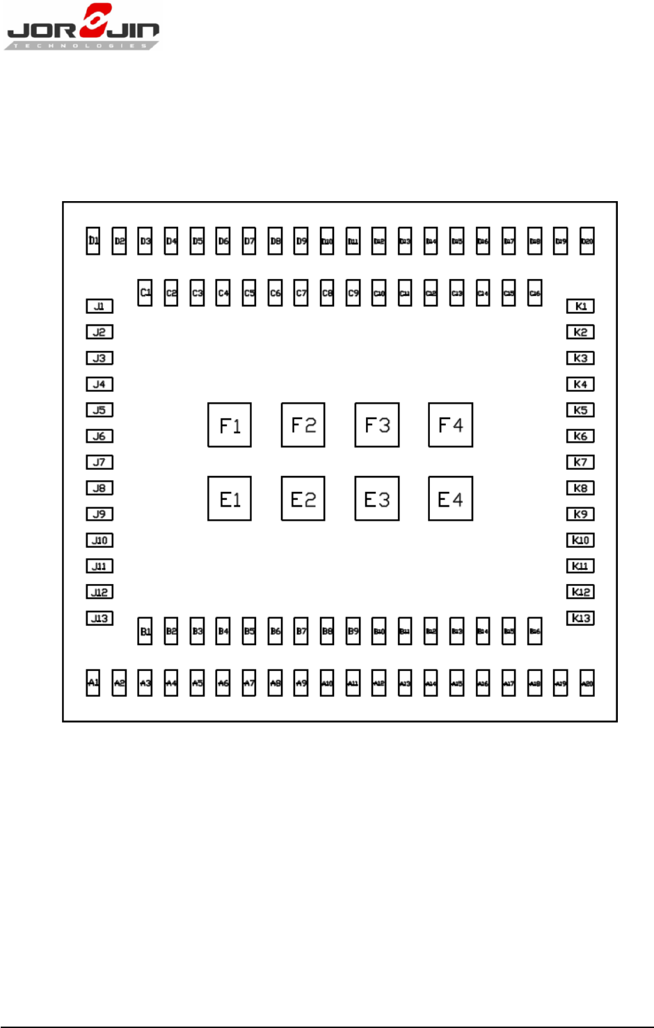
3. MODULE OUTLINE
3.1. Signal Layout (Top View)
Figure 3-1 Device pins

Doc No: WG7833-B0-DTS-R03
Copyright
©
JORJIN TECHNOLOGIES INC. 2015
http://WWW.JORJIN.COM.TW
CONFIDENTIAL
Page 9
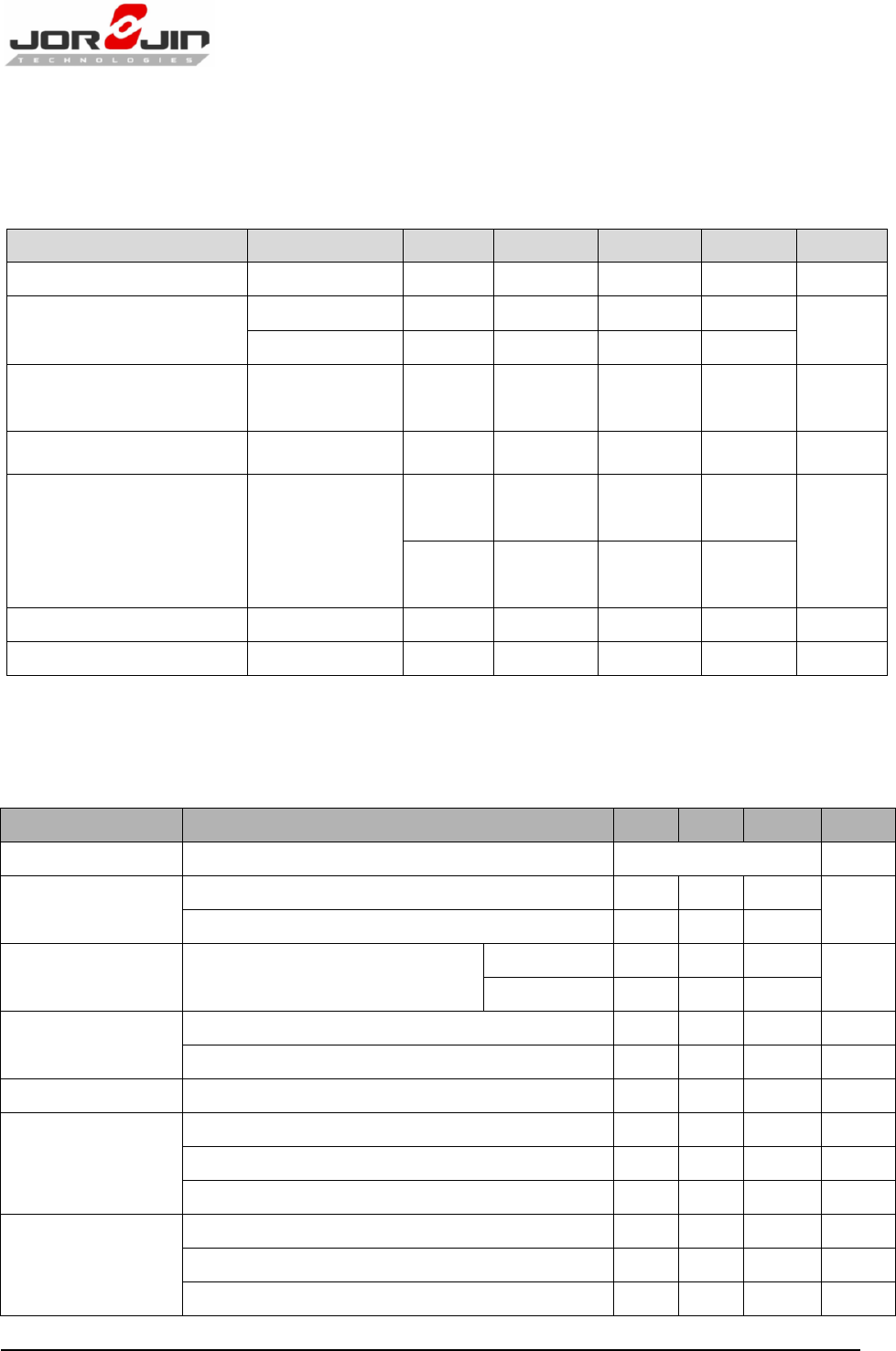
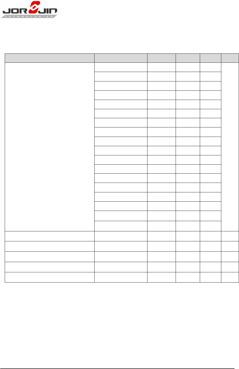
3.2. Pin Description
Table 3-1. Pin Description
Pin
No.
Signal Name Type
Shut
Down
state
After
Power
Up
(1)
Voltage
Level Description
A1
GND GND
Ground
A2
WLAN_SDIO_D3 IO HiZ PU 1.8V
WLAN SDIO Data bit 3. Changes state to
PU at WL_EN or BT_EN assertion for
card detects. Later disabled by software
during initialization.
(2)
A3
WLAN_SDIO_CMD
I/O HiZ HiZ 1.8V WLAN SDIO Command
(2)
A4
WLAN_SDIO_D2 IO HiZ HiZ 1.8V WLAN SDIO Data bit 2
(2)
A5
WLAN_SDIO_D0 IO HiZ HiZ 1.8V WLAN SDIO Data bit 0
2)
A6
WLAN_SDIO_D1 IO HiZ HiZ 1.8V WLAN SDIO Data bit 1
(2)
A7
WLAN_SDIO_CLK IN HiZ HiZ 1.8V WLAN SDIO Clock. Must be driven by
the host.
A8
GND GND
Ground
A9
BT_HCI_CTS
IN PU PU 1.8V UART CTS from host.
NC if not used.
A10
BT_HCI_RTS
OUT
PU PU 1.8V UART RTS to host.
NC if not used.
A11
BT_HCI_TX
OUT
PU PU 1.8V UART TX to host.
NC if not used.
A12
BT_HCI_RX
IN PU PU 1.8V UART RX from host.
NC if not used.
A13
NC
NC
A14
NC
NC
A15
NC
NC
A16
GND GND
Ground
A17
NC
NC
A18
GND GND
Ground

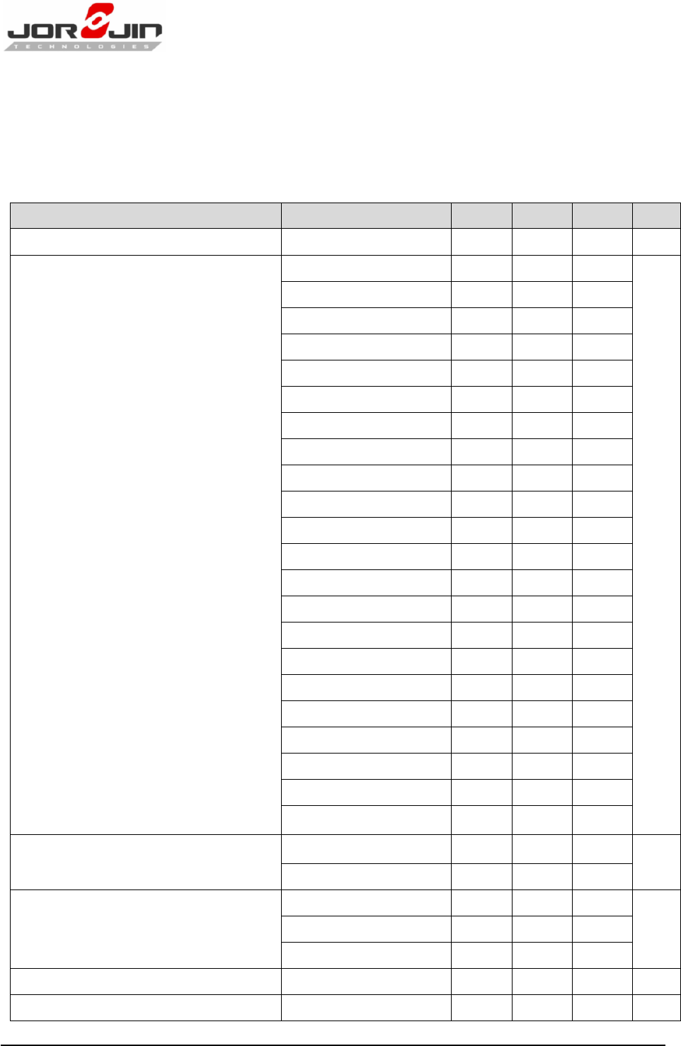
Doc No: WG7833-B0-DTS-R03
Copyright
©
JORJIN TECHNOLOGIES INC. 2015
http://WWW.JORJIN.COM.TW
CONFIDENTIAL
Page 10
A19
VIO_IN
POW
PD PD 1.8V Connect to 1.8V external VIO
A20
GND GND
Ground
B1
NC
NC
B2
NC
NC
B3
GPIO11 I/O PU PU 1.8V Reserved for future use. NC if not used.
B4
GPIO9 I/O PU PU 1.8V Reserved for future use. NC if not used.
B5
GPIO10 I/O PU PU 1.8V Reserved for future use. NC if not used.
B6
GPIO12 I/O PU PU 1.8V Reserved for future use. NC if not used.
B7
NC
NC
B8
NC
NC
B9
NC
NC
B10
NC
NC
B11
NC
NC
B12
NC
NC
B13
NC
NC
B14
NC
NC
B15
NC
NC
B16
NC
NC
C1
GND GND
Ground
C2
NC
NC
C3
NC
NC
C4
BT_UART_DEBUG
OUT
PU PU 1.8V Option: Bluetooth logger
C5
NC
NC
C6
WLAN_UART_DBG
OUT
PU PU 1.8V Option: WLAN logger
C7
GPIO1
I/O PD PD 1.8V WL_RS232_TX (when IRQ_WL = 1 at
power up)
C8
NC
NC
C9
TCXO_CLK_IN
ANA
TCXO clock input
C10
WLAN_EN
IN PD PD 1.8V Mode setting: High = enable
C11
WLAN_IRQ
OUT
PD 0 1.8V
SDIO available, interrupt out. Active
high. To use WL_RS232_TX and RX
lines, need to pull up with 10K
resistor.
C12
GND
GND
Ground

Doc No: WG7833-B0-DTS-R03
Copyright
©
JORJIN TECHNOLOGIES INC. 2015
http://WWW.JORJIN.COM.TW
CONFIDENTIAL
Page 11
C13
GND
GND
Ground
C14
GND
GND
Ground
C15
GND
GND
Ground
C16
GND
GND
Ground
D1
GND
GND
Ground
D2
VBAT
POW
VBAT Power supply input, 2.9 to 4.8 V
D3
NC
NC
D4
NC
NC
D5
NC
NC
D6
GND
GND
Ground
D7
NC
NC
D8
GND
GND
Ground
D9
PA_DC2DC_OUT
POW
Internal DC2DC output
D10
GPIO4
I/O PD PD 1.8V
Reserved for future use. NC if not used.
D11
GPIO2
I/O PD PD 1.8V WL_RS232_RX (when IRQ_WL = 1 at
power up)
D12
BT_EN
In PD PD 1.8V Mode setting: High = enable
D13
NC
NC
D14
NC
NC
D15
GND
GND
Ground
D16
GND
GND
Ground
D17
GND
GND
Ground
D18
GND
GND
Ground
D19
RF_ANT_WA RF WLAN 5G RF Port
D20
GND
GND
Ground
E1
GND
GND
Ground
E2
GND
GND
Ground
E3
GND
GND
Ground
E4
GND
GND
Ground
F1
GND
GND
Ground
F2
GND
GND
Ground
F3
GND
GND
Ground
F4
GND
GND
Ground
J1
GND
GND
Ground
J2
GND
GND
Ground

Doc No: WG7833-B0-DTS-R03
Copyright
©
JORJIN TECHNOLOGIES INC. 2015
http://WWW.JORJIN.COM.TW
CONFIDENTIAL
Page 12
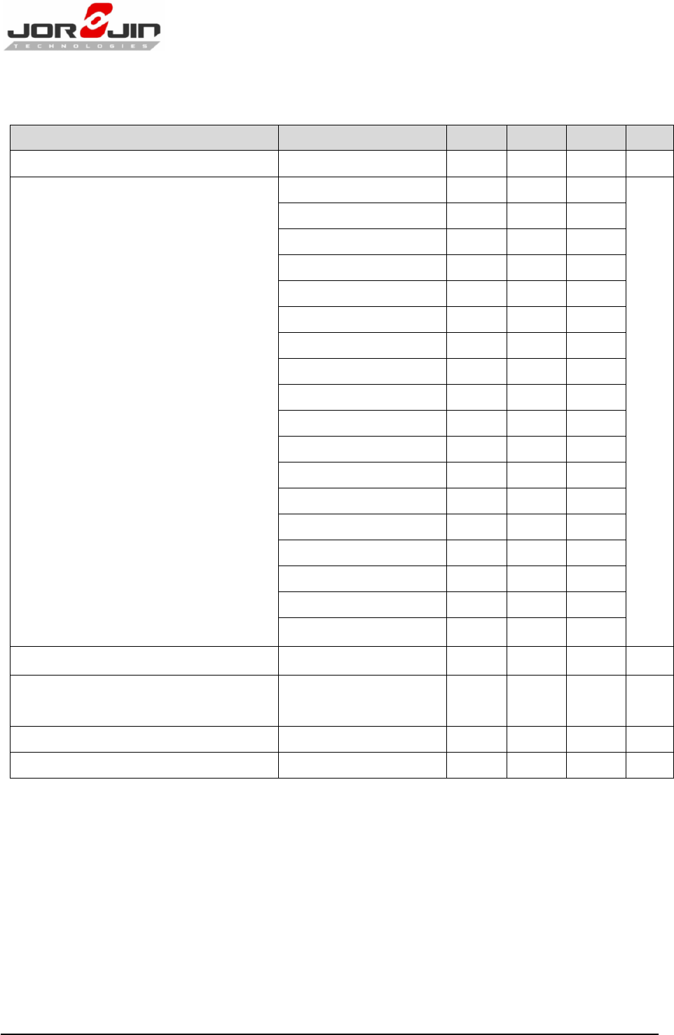
J3
GND
GND
Ground
J4
NC
NC
J5
NC
NC
J6
NC
NC
J7
NC
NC
J8
NC
NC
J9
NC
NC
J10
CLK_REQ_OUT
OUT
PD PD 1.8V TCXO clock request out
J11
GND
GND
Ground
J12
GND
GND
Ground
J13
NC
NC
K1
GND
GND
Ground
K2
RF_ANT_BG
RF WLAN/BT 2.4G RF Port
K3
GND
GND
Ground
K4
GND
GND
Ground
K5
GND
GND
Ground
K6
GND
GND
Ground
K7
BT_AUD_OUT
OUT
PD PD 1.8V Bluetooth PCM/I2S Bus. Data out.
NC if not used.
K8
GND
GND
Ground
K9
EXT_32K
ANA
Input Sleep clock: 32.768 KHz
K10
GND
GND
Ground
K11
BT_AUD_IN
IN PD PD 1.8V Bluetooth PCM/I2S Bus. Data in.
NC if not used.
K12
BT_AUD_CLK
OUT
PD PD 1.8V Bluetooth PCM/I2S Bus. Clock.
NC if not used.
K13
BT_AUD_FSYNC
OUT
PD PD 1.8V Bluetooth PCM/I2S Bus. Frame sync.
NC if not used.
(1) PU=pull up; PD=pull down.
(2) Host must provide PU for all non-CLK SDIO signals
Doc No: WG7833-B0-DTS-R03
Copyright
©
JORJIN TECHNOLOGIES INC. 2015
http://WWW.JORJIN.COM.TW
CONFIDENTIAL
Page 13
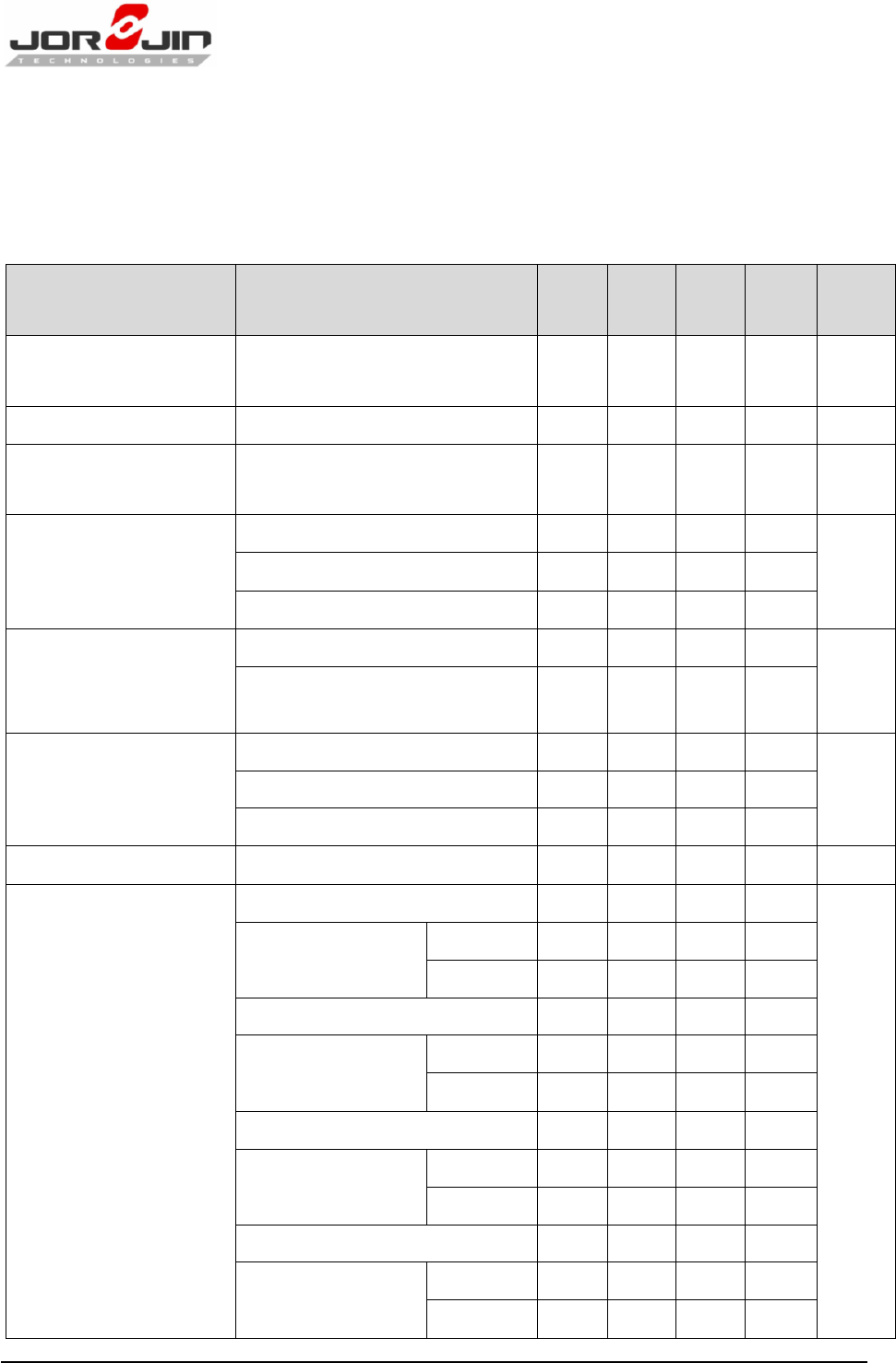
4. MODULE SPECIFICATION
4.1. General Module Requirements and Operation
4.1.1. Absolute Maximum Ratings
(1)
1) Stresses beyond those listed under “absolute maximum ratings” may cause permanent damage to the device. These
are stress ratings only and functional operation of the device at these or any other conditions beyond those indicated
under “operating conditions” is not implied. Exposure to absolute-maximum-rated conditions for extended periods may
affect device reliability.
2) 5.5V up to 10s cumulative in 7 years, 5V cumulative to 250s, 4.8V cumulative to 2.33 years - all includes charging
dips and peaks.
3) Operating free-air temperature range. The device can be reliably operated for 7 years at ambient of 85°C, assuming
25% active mode and 75% sleep mode (15,400 cumulative active power-on hours).
4) Electrostatic discharge (ESD) to measure device sensitivity/immunity to damage caused by electrostatic discharges
into device.
5) Level listed is the passing level per ANSI/ESDA/JEDEC JS-001. JEDEC document JEP155 states that 500V HBM allows
safe manufacturing with a standard ESD control process, and manufacturing with less than 500V HBM is possible if
necessary precautions are taken. Pins listed as 1000V may actually have higher performance.
6) Level listed is the passing level per EIA-JEDEC JESD22-C101E. JEDEC document JEP157 states that 250 V CDM allows
safe manufacturing with a standard ESD control process, and manufacturing with less than 250V CDM is possible if
necessary precautions are taken. Pins listed as 250 V may actually have higher performance
Parameter Value Units
VBAT -0.5 to 5.5
(2)
V
VIO -0.5 to 2.1 V
Input voltage to Analog pins -0.5 to 2.1 V
Input voltage limits (CLK_IN) -0.5 to VDD_IO V
Input voltage to all other pins -0.5 to (VDD_IO + 0.5V) V
Operating ambient temperature range -40 to +85
(3)
°C
Storage temperature range -55 to +125 °C
ESD Stress Voltage
(4)
Human Body Model
(5)
>1000 V
Charged Device Model
(6)
>250 V
Doc No: WG7833-B0-DTS-R03
Copyright
©
JORJIN TECHNOLOGIES INC. 2015
http://WWW.JORJIN.COM.TW
CONFIDENTIAL
Page 14
4.1.2. Recommended Operating Conditions
Parameter Condition Sym Min Max Units
VBAT
(1)
DC supply range
for all modes
2.9 4.8 V
1.8 V IO ring power supply voltage
1.62 1.95
IO high-level input voltage VIH 0.65 x VDD_IO VDD_IO
IO low-level input voltage VIL 0 0.35 x VDD_IO
Enable inputs high-level input
voltage
VIH_EN
1.365 VDD_IO
Enable inputs low-level input
voltage
VIL_EN
0 0.4
High-level output voltage @ 4 mA VOH VDD_IO -0.45 VDD_IO
@ 1 mA VDD_IO -0.112
VDD_IO
@ 0.3 mA VDD_IO -0.033
VDD_IO
Low-level output voltage @ 4 mA VOL 0 0.45
@ 1 mA 0 0.112
@ 0.09 mA 0 0.01
Input transitions time Tr/Tf from
10% to 90% (Digital IO)
(2)
Tr/Tf 1 10 ns
Output rise time from 10% to 90%
(Digital pins)
(2)
CL < 25 pF Tr 5.3 ns
Output fall time from 10% to 90%
(Digital pins)
(2)
CL < 25 pF Tf 4.9
Ambient operating temperature -40 85 ºC
Maximum power dissipation WLAN operation
2.8 W
BT operation 0.2
(1) 4.8V is applicable only for 2.3 years (30% of the time). Otherwise, the maximum VBAT should not exceed 4.3V.
(2) Applies to all Digital lines except SDIO, UART, I2C, PCM and slow clock lines
Doc No: WG7833-B0-DTS-R03
Copyright
©
JORJIN TECHNOLOGIES INC. 2015
http://WWW.JORJIN.COM.TW
CONFIDENTIAL
Page 15
4.1.3. External Slow Clock Input (SLOW_CLK)
The supported digital slow clock is 32.768 kHz digital (square wave).
Parameter Condition Sym Min. Typ. Max. Units
Input slow clock Frequency 32.768 KHz
Input slow clock accuracy
(Initial + temp + aging)
WLAN, BT +/-250
ppm
ANT +/- 50
Input Transition time Tr/Tf
- 10% to 90%
Tr/Tf 100 ns
Frequency input duty Cycle 15 50 85 %
Input Voltage Limits
Square Wave,
DC-coupled
Vih
0.65x
VDD_IO
VDD_IO
Vpeak
Vil 0
0.35x
VDD_IO
Input Impedance 1 MΩ
Input Capacitance 5 pF
4.1.4. External Fast Clock Requirements (-40 to +85°
°°
°C)
Parameter Condition Min.
Typ.
Max. Unit
Frequency 26 MHz
Frequency Accuracy Short term (voltage and temp. effect) ± 20
ppm
Long term (including aging) ± 20
Input voltage limits
(TCXO_CLK_IN)
Sine wave/ clipped sine wave,
ac-coupled
2.4GHz WLAN
0.2 1.4
Vp-p
5GHz WLAN 0.8 1.4
Input impedance Input resistance 20 KΩ
Input capacitance 2.5 pF
Power-up time
(1)
5 ms
Phase noise 2.4GHz
for 26MHz, 20MHz
SISO
Measured at 1 KHz offset -123.4
dBc/Hz
Measured at 10 KHz offset -133.4
dBc/Hz
Measured at 100 KHz offset -138.4
dBc/Hz
Phase noise 2.4GHz
for 26MHz, 40MHz
SISO
Measured at 1 KHz offset -128.4
dBc/Hz
Measured at 10 KHz offset -135.4
dBc/Hz
Measured at 100 KHz offset -139.9
dBc/Hz

Doc No: WG7833-B0-DTS-R03
Copyright
©
JORJIN TECHNOLOGIES INC. 2015
http://WWW.JORJIN.COM.TW
CONFIDENTIAL
Page 16
Phase noise 5GHz for
26MHz, 20/40 MHz
SISO
Measured at 1 KHz offset -128.4
dBc/Hz
Measured at 10 KHz offset -145.4
dBc/Hz
Measured at 100 KHz offset -148.4
dBc/Hz
(1) Power-up time is calculated from the time CLK_REQ_OUT asserted till the time the TCXO_CLK amplitude is within
voltage limit specified above and TCXO_CLK frequency is within 0.1 ppm of final steady state frequency.
Doc No: WG7833-B0-DTS-R03
Copyright
©
JORJIN TECHNOLOGIES INC. 2015
http://WWW.JORJIN.COM.TW
CONFIDENTIAL
Page 17
4.2. WLAN RF Performance
4.2.1. WLAN 2.4-GHz Receiver Characteristics
Parameter Condition Min Typ Max Units
Operation frequency range 2412 2484 MHz
Sensitivity
20MHz Bandwidth
At < 10% PER limit
1 Mbps DSSS -96.3 -93.4 dBm
2 Mbps DSSS -93.2 -90.5
5.5 Mbps CCK -90.6 -87.9
11 Mbps CCK -87.9 -85.7
6 Mbps OFDM -92 -89.2
9 Mbps OFDM -90.4 -87.7
12 Mbps OFDM -89.5 -86.8
18 Mbps OFDM -87.2 -84.5
24 Mbps OFDM -84.1 -81.4
36 Mbps OFDM -80.7 -78
48 Mbps OFDM -76.5 -73.8
54 Mbps OFDM -74.9 -72.4
MCS0 MM 4K -90.4 -87.4
MCS1 MM 4K -87.6 -84.9
MCS2 MM 4K -85.9 -83.2
MCS3 MM 4K -82.8 -80.1
MCS4 MM 4K -79.4 -76.7
MCS5 MM 4K -75.2 -72.5
MCS6 MM 4K -73.5 -70.8
MCS7 MM 4K -72.4 -69.7
MCS0 MM 4K 40MHz -87.4 -82.7
MCS7 MM 4K 40MHz -69 -65.5
Max Input Level
At < 10% PER limit
OFDM(11g/n) -19 -9
dBm
CCK -4 0
Adjacent channel rejection
Sensitivity level +3dB for OFDM, Sensitivity
level +6dB for 11b
2Mbps DSSS 42.7
dBm
11Mbps CCK 37.9
54Mbps OFDM 2.0
LO Leakage -80 dBm
PER Floor 1.0 2.0 %
Doc No: WG7833-B0-DTS-R03
Copyright
©
JORJIN TECHNOLOGIES INC. 2015
http://WWW.JORJIN.COM.TW
CONFIDENTIAL
Page 18
4.2.2. WLAN 2.4-GHz Transmitter Power
Parameter
Condition
Min Typ Max
Output Power
- Maximum RMS output power
measured at 1dB from IEEE
spectral mask or EVM
1 Mbps DSSS 15 17
– dBm
2 Mbps DSSS 15 17
–
5.5 Mbps CCK 15 17
–
11 Mbps CCK 15 17
–
6 Mbps OFDM 15 17
–
9 Mbps OFDM 15 17
–
12 Mbps OFDM 15 17
–
18 Mbps OFDM 15 17
–
24 Mbp
S
OFDM 14 16.2
–
36 Mbps OFDM 13.1 15.3
–
48 Mbps OFDM 12.4 14.6 –
54 Mbps OFDM 11.8 13.8
–
MCS0 MM 13.9 16.1
MCS1 MM 13.9 16.1
MCS2 MM 13.9 16.1
MCS3 MM 13.9 16.1
MCS4 MM 13.3 15.3
MCS5 MM 12.4 14.6
MCS6 MM 11.8 13.8
MCS7 MM 10.6 12.6
MCS0 MM 40MHz 12.3 14.8
MCS7 MM 40MHz 10.2 12.2
Output power accuracy -1.5 +1.5 dB
Output power resolution 0.125 dB
Operation frequency range 2412 2484 MHz
Return loss -10 dB
Reference input impedance 50 Ω
Doc No: WG7833-B0-DTS-R03
Copyright
©
JORJIN TECHNOLOGIES INC. 2015
http://WWW.JORJIN.COM.TW
CONFIDENTIAL
Page 19
4.2.3. WLAN 5-GHz Receiver Characteristics (For WG7833/03 Only)
Parameter Condition Min Typ Max Units
Operation frequency range 4910 5825 MHz
Sensitivity
- 20MHz bandwidth.
- At < 10% PER limit
6 Mbps OFDM – -91.5
-87.6
dBm
9 Mbps OFDM – -89.7
-85.7
12 Mbps OFDM – -88.9
-84.9
18 Mbps OFDM – -86.4
-82.4
24 Mbps OFDM – -83.3
-79.3
36 Mbps OFDM – -79.9
-75.9
48 Mbps OFDM – -75.6
-71.6
54 Mbps OFDM – -74.0
-70.5
MCS0 MM 4K – -89.8
-85.4
MCS1 MM 4K – -87.0
-83.0
MCS2 MM 4K – -85.2
-81.2
MCS3 MM 4K – -82.1
-78.1
MCS4 MM 4K – -78.7
-74.7
MCS5 MM 4K – -74.4
-70.4
MCS6 MM 4K – -72.8
-68.8
MCS7 MM 4K – -71.5
-67.9
MCS0 MM 4K 40MHz –
-87.0
-81.8
MCS7 MM 4K 40MHz –
-68.3
-64.4
Max Input Level, At < 10% PER limit OFDM(11a/n) -27 -9
dBm
Adjacent channel rejection
Sensitivity level +3dB for OFDM
54Mbps OFDM 2
dBm
LO Leakage -53 dBm
PER Floor 1.0 2.0 %
Doc No: WG7833-B0-DTS-R03
Copyright
©
JORJIN TECHNOLOGIES INC. 2015
http://WWW.JORJIN.COM.TW
CONFIDENTIAL
Page 20
4.2.4. WLAN 5-GHz Transmitter Power (For WG7833/03 Only)
Parameter
Condition
Min Typ Max
Output Power
- Maximum RMS output power
measured at 1dB from IEEE
spectral mask or EVM
6 Mbps OFDM 14.7 16.8
– dBm
9 Mbps OFDM 14.7 16.8
–
12 Mbps OFDM 14.7 16.8
–
18 Mbps OFDM 14.7 16.8
–
24 Mbp
S
OFDM 14.1 15.7
–
36 Mbps OFDM 13.4 15.0
–
48 Mbps OFDM 12.6 14.2
–
54 Mbps OFDM 11.6 13.4
–
MCS0 MM 14.4 16.4
MCS1 MM 14.4 16.4
MCS2 MM 14.4 16.4
MCS3 MM 14.4 16.4
MCS4 MM 13.2 15.0
MCS5 MM 12.6 14.2
MCS6 MM 11.6 13.4
MCS7 MM 10.7 12.4
MCS0 MM 40MHz 13.0 15.9
MCS7 MM 40MHz 9.7 11.6
Output power accuracy -1.5 +1.5 dB
Output power resolution 0.125 dB
Operation frequency range 4910 5825 MHz
Return loss -10 dB
Reference input impedance 50 Ω
Doc No: WG7833-B0-DTS-R03
Copyright
©
JORJIN TECHNOLOGIES INC. 2015
http://WWW.JORJIN.COM.TW
CONFIDENTIAL
Page 21
4.3. Bluetooth RF Performance (For WG7833/31 Only)
4.3.1. BT Receiver Characteristics, In-Band Signals
Parameter Condition Min
Typ Max
BT
Spec
Units
BT BR, EDR operation
frequency range
2402 2480 MHz
BT BR, EDR channel spacing
1 MHz
BT BR, EDR input
impedance
50 Ω
BT BR, EDR sensitivity
(1)
Dirty TX on
BR, BER = 0.1%
-92.0
-70 dBm
EDR2, BER = 0.01%
-91.5
-70
EDR3, BER = 0.01%
-84.5
-70
BT EDR BER floor at
sensitivity + 10 dB, dirty TX
off (for 1,600,000 bits)
EDR2 1e-6
1e-5
EDR3 1e-6
1e-5
BT BR, EDR maximum
useable input power
BR, BER = 0.1% -5.0
-20 dBm
EDR2, BER = 0.1% -10.0
-20
EDR3, BER = 0.1% -10.0
-20
BT BR intermodulation Level of interferers For n = 3, 4, and 5
-36.0
-30.0
-39 dBm
BT BR, EDR C/I performance
Numbers show
wanted-signal to
interfering-signal ratio.
Smaller numbers indicate
better C/I performances
(Image frequency = -1MHz)
BR, Co-channel 8.0
11 dB
EDR, Co-channel EDR2 9.5
13
EDR3 16.5
21
BR, adjacent ±1 MHz -10.0
0
EDR, adjacent ±1 MHz,
(image)
EDR2 -10.0
0
EDR3 -5.0
5
BR, adjacent +2 MHz -38.0
-30
EDR, adjacent +2 MHz,
EDR2 -38.0
-30
EDR3 -38.0
-25
BR, adjacent -2 MHz -28.0
-20
EDR, adjacent
-2 MHz
EDR2 -28.0
-20
EDR3 -22.0
-13
Doc No: WG7833-B0-DTS-R03
Copyright
©
JORJIN TECHNOLOGIES INC. 2015
http://WWW.JORJIN.COM.TW
CONFIDENTIAL
Page 22
BR, adjacent ≥Ι±3Ι MHz -45.0
-40
EDR, adjacent ≥Ι±3Ι
MHz
EDR2 -45.0
-40
EDR3 -44.0
-33
BT BR, EDR RF return loss -10.0 dB
(1) Sensitivity degradation up to -3dB may occur due to fast clock harmonics with dirty TX on.
4.3.2. BT Receiver Characteristics – General Blocking
Parameter Condition Min Typ BT spec
Units
Blocking performance over full range,
according to BT specification
(1)
30-2000 MHz -6 -10 dBm
2000-2399 MHz -6 -27
2484-3000 MHz -6 -27
3-12.75 GHz -6 -10
1) Exceptions taken out of the total 24 allowed in the BT spec.
4.3.3. BT Receiver Characteristics –BR, EDR Blocking Per Band
Parameter Band Min Typ Units
Blocking performance for various cellular
bands
Hopping on.
Wanted signal: -3dB from sensitivity, with
modulated continuous blocking signal.
BER = 0.1% for BT BR, 0.01% for BT EDR.
PER = 1%
776-794 MHz (CDMA) -12
dBm
824-849 MHz (GMSK)
(1)
-3
824-849 MHz (EDGE)
(1)
-11
824-849 MHz (CDMA, QPSK)
(1)
-12
880-915 MHz (GMSK) -14
880-915 MHz (EDGE) -15
1710-1785 MHz (GMSK) -4
1710-1785 MHz (EDGE) -18
1850-1910 MHz (GMSK) -18
1850-1910 MHz (EDGE) -20
1850-1910 MHz (CDMA, QPSK) -20
1850-1910 MHz (WCDMA, QPSK) -16
1920-1980 MHz (WCDMA, QPSK) -17
1) Except for frequencies where [3 * F_BLOCKER] falls within the BT band (2400-2483.5 MHz)
Doc No: WG7833-B0-DTS-R03
Copyright
©
JORJIN TECHNOLOGIES INC. 2015
http://WWW.JORJIN.COM.TW
CONFIDENTIAL
Page 23
4.3.4. BT Transmitter, BR
Parameter Min Typ Max BT Spec
Units
BR RF output power
(1)
VBAT >= 3V
12.5
dBm
VBAT < 3V
7.0
BR Gain Control Range 30 dB
BR Power Control Step 2 5
8
2 to 8
BR Adjacent Channel Power |M-N| = 2
(2)
-43.0
≤ -20 dBm
BR Adjacent Channel Power |M-N| > 2
(2)
-48.0
≤ -40
1) Values reflect maximum power. Reduced power is available using a vendor-specific (VS) command.
2) Assumes 3dB insertion loss on external filter and traces
4.3.5. BT Transmitter, EDR
Parameter Min Typ Max BT Spec
Units
EDR output power
(1)
VBAT >= 3V
7
dBm
VBAT < 3V
5
EDR relative power -2 1 -4 to +1 dB
EDR Gain Control Range 30 dB
EDR Power Control Step 2 5
8
2 to 8 dB
EDR Adjacent Channel Power |M-N| = 1
(2)
-36
≤ -26 dBc
EDR Adjacent Channel Power |M-N| = 2
(2)
-30
≤ -20 dBm
EDR Adjacent Channel Power |M-N| > 2
(2)
-42
≤ -40
1) Values reflect maximum power. Reduced power is available using a vendor-specific (VS) command.
2) Assumes 3dB insertion loss on external filter and traces.
4.3.6. BT Modulation, BR
Parameter Condition
(1)
Performances BT
spec
Units
Min
Typ
Max
BR -20dB Bandwidth 925
995
≤1000
kHz
BR modulation
characteristics
∆f1avg
Mod data = 4-ones,
4-zeros: 111100001111...
160
140 to
175
kHz
∆f2max ≥ limit for
at least 99.9% of all
Δf2max
Mod data = 1010101...
130
> 115
kHz
∆f2avg / ∆f1avg
88
> 80 %
Doc No: WG7833-B0-DTS-R03
Copyright
©
JORJIN TECHNOLOGIES INC. 2015
http://WWW.JORJIN.COM.TW
CONFIDENTIAL
Page 24
BR carrier frequency
drift
One slot packet -25
+25
< ±25
kHz
Three and five slot packet -35
35
< ±40
kHz
BR drift rate lfk+5 – fkl , k = 0 …. max
15
< 20 kHz/
50μs
BR initial carrier
frequency tolerance
(2)
f0 – fTX -25
25 < ±75
kHz
1) Performance figures at maximum power
2) This number is added on top of the reference clock frequency accuracy
4.3.7. BT Modulation, EDR
Parameter
(1)
Condition Min
Typ.
Max
BT spec
Units
EDR Carrier frequency stability -5
5
≤10 kHz
EDR Initial Carrier Frequency Tolerance
(2)
-25
25
±75 kHz
EDR RMS DEVM EDR2 4
20 %
EDR3 4
13 %
EDR 99% DEVM EDR2 30
30 %
EDR3 20
20 %
EDR Peak DEVM EDR2 9
35 %
EDR3 9
25 %
1) Performance figures at maximum power
2) This number is added on top of the reference clock frequency accuracy
4.3.8. BT BR, EDR Transceiver - Emissions
Parameter
(1)
Condition
(2)
Performances Units
Min Typ Max
BT out-of-band
emission
746-768 MHz (CDMA) BR, EDR -151
dBm/Hz
869-894 MHz (WCDMA, GSM) -149
dBm/Hz
925-960 MHz (E-GSM) -148
dBm/Hz
1570-1580 MHz (GPS) -145
dBm/Hz
1598-1607 MHz (GLONASS) (3) -145
dBm/Hz
1805-1880 MHz (DCS, WCDMA)
-141
dBm/Hz
1930-1990 MHz (PCS) -139
dBm/Hz
Doc No: WG7833-B0-DTS-R03
Copyright
©
JORJIN TECHNOLOGIES INC. 2015
http://WWW.JORJIN.COM.TW
CONFIDENTIAL
Page 25
2110-2170 MHz (WCDMA) BR -134
dBm/Hz
EDR -129
dBm/Hz
BT harmonics 2nd harmonic 1.5
dBm
3rd harmonic -4
dBm
4th harmonic -10
dBm
1) Meets FCC and ETSI requirements with suitable external filter
2) Performance figures at maximum power
3) Except for frequencies that corresponds to 2*RF_FREQ/3
4.3.9. BT BR Transceiver - Spurs
Parameter
(1)
Condition
(2)
Performances Units
Min Typ Max
BT out-of-band spurs 76-108 MHz (FM) BR -77
dBm
746-768 MHz (WCDMA) -79
dBm
869-894 MHz (WCDMA, GSM) -77
dBm
925-960 MHz (E-GSM) -77
dBm
1570-1580 MHz (GPS) -72
dBm
1598-1607 MHz (GLONASS) (3) -74
dBm
1805-1880 MHz (DCS, WCDMA) -72
dBm
1930-1990 MHz (PCS) -70
dBm
2110-2170 MHz (WCDMA) -59
dBm
1) Meets FCC and ETSI requirements with suitable external filter
2) Performance figures at maximum power
3) Except for frequencies that corresponds to 2*RF_FREQ/3
4.3.10. BT EDR Transceiver - Spurs
Parameter
(1)
Condition
(2)
Performances Units
Min Typ Max
BT out-of-band spurs 76-108 MHz (FM) EDR -82
dBm
746-768 MHz (WCDMA) -87
dBm
869-894 MHz (WCDMA, GSM)
-85
dBm
925-960 MHz (E-GSM) -84
dBm
1570-1580 MHz (GPS) -79
dBm
Doc No: WG7833-B0-DTS-R03
Copyright
©
JORJIN TECHNOLOGIES INC. 2015
http://WWW.JORJIN.COM.TW
CONFIDENTIAL
Page 26
1598-1607 MHz (GLONASS)
(3)
-78
dBm
1805-1880 MHz (DCS, WCDMA)
-76
dBm
1930-1990 MHz (PCS) -74
dBm
2110-2170 MHz (WCDMA) -63
dBm
1) Meets FCC and ETSI requirements with suitable external filter
2) Performance figures at maximum power
3) Except for frequencies that corresponds to 2*RF_FREQ/3
4.4. BT LE RF Performance
4.4.1. BT LE Receiver Characteristics, In-Band Signals
Parameter Condition
(2)
Min
Typ
Max
BLE spec
Units
BT LE Operation frequency range 2402
2480
MHz
BT LE Channel spacing 2 MHz
BT LE Input impedance 50 Ω
BT LE Sensitivity
(1)
, Dirty Tx on
-93
≤ -70 dBm
BT LE Maximum useable input power
-5 ≥ -10 dBm
BT LE Intermodulation characteristics
Level of interferers. For
n = 3, 4, 5
-36
-30
≥ -50 dBm
BT LE C/I performance Note:
Numbers show wanted
signal-to-interfering signal ratio.
Smaller numbers indicate better C/I
performance. Image = -1MHz
LE, co-channel 8
12
≤ 21 dB
LE, adjacent ±1MHz -5
0
≤ 15
LE, adjacent +2MHz -45
-38
≤ -17
LE, adjacent –2MHz -22
-15
≤ -15
LE, adjacent ≥ |±3|MHz
-47
-40
≤ -27
1) Sensitivity degradation up to -3dB may occur due to fast clock harmonics.
2) BER of 0.1% corresponds to PER of 30.8% for a minimum of 1500 transmitted packets, according to BT LE test spec
4.4.2. BT LE Receiver Characteristics – General Blocking
Parameter Condition Min Typ Max BLE
spec
Unit
BT LE Blocking performance over
full range, according to LE
specification
(1)
30–2000MHz -15
≥ –30 dBm
2000–2399MHz -15
≥ –35
2484–3000MHz -15
≥ –35
Doc No: WG7833-B0-DTS-R03
Copyright
©
JORJIN TECHNOLOGIES INC. 2015
http://WWW.JORJIN.COM.TW
CONFIDENTIAL
Page 27
3–12.75GHz -15
≥ –30
1) Exceptions taken out of the total 10 allowed for fbf_1, according to the BT LE Spec
4.4.3. BT LE Transmitter Characteristics
Parameter Min Typ Max BT LE
Spec
Unit
BT LE RF output power
(1)
Vbat >= 3V
12.5
≤10 dBm
Vbat < 3V
870
≤10 dBm
BT LE Adjacent Channel Power |M-N| = 2
(2)
-51.0
≤ –20 dBm
BT LE Adjacent Channel Power |M-N| > 2
(2)
-54.0
≤ –30
1) To reduce the maximum BLE power, use a VS command. The optional extra margin is offered to compensate for
design losses, such as trace and filter losses, and to achieve the maximum allowed output power at system level.
2) Assumes 3dB insertion loss on external filter and traces
4.4.4. BT LE Modulation Characteristics
Parameter Condition
(1)
Performances BT
Spec
Units
Min
Typ
Max
BT LE modulation
characteristics
∆f1avg
Mod data =
4-ones, 4-zeros:
111100001111...
250
225 to
275
kHz
∆f2max ≥ limit for at
least 99.9% of all Δf2max
Mod data =
1010101...
215
≥185
kHz
∆f2avg / ∆f1avg
90
≥80 %
BT LE carrier frequency
drift
lf0 – fnl , n = 2,3 …. K -25 25 ≤±50
kHz
BT LE drift rate lf1 – f0l and lfn – fn-5l ,n = 6,7…. K 15 ≤20
kHz/
50μs
LE initial carrier
frequency tolerance
(2)
fn – fTX -25 25 ≤±100
kHz
1) Performance figures at maximum power
2) This number is added on top of the reference clock frequency accuracy
Doc No: WG7833-B0-DTS-R03
Copyright
©
JORJIN TECHNOLOGIES INC. 2015
http://WWW.JORJIN.COM.TW
CONFIDENTIAL
Page 28
4.4.5. BT LE Transceiver – Emissions
See Section 4.3.8, BT BR, EDR Transceiver – Emissions.
4.4.6. BT LE Transceiver - Spurs
See Section 4.3.9, BT BR Transceiver – Spurs.
4.5. ANT Performance
4.5.1. ANT Receiver Characteristics, In-Band Signals
Parameter Condition Min Typ Max
Units
ANT Operation frequency range 2402
2480
MHz
ANT Channel spacing 1 MHz
ANT Sensitivity 12.72% PER
(1)
-85 dBm
1) Translation from BER=0.1%, assuming packet is 136 bits ( not including preamble )
4.5.2. ANT Transmitter Characteristics
Same as Bluetooth BR Transmitter Characteristics
Doc No: WG7833-B0-DTS-R03
Copyright
©
JORJIN TECHNOLOGIES INC. 2015
http://WWW.JORJIN.COM.TW
CONFIDENTIAL
Page 29
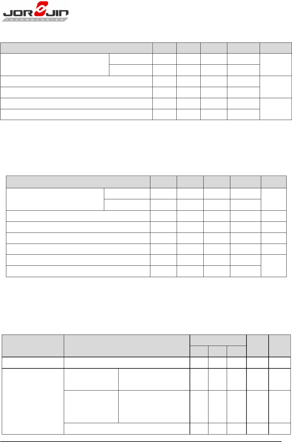
4.6. POWER CONSUMPTION
4.6.1. Shutdown and Sleep Currents
Parameter Power Supply Current Typ Unit
Shutdown mode
All functions shut down.
VBAT 10
uA
VIO 2
WLAN sleep mode VBAT 154
BT sleep mode VBAT 110
4.6.2. WLAN Power Currents
Parameter
Conditions Typ (avg) - 25C
Units
LPM 2.4GHz RX LPM 43
mA
Receiver
2.4GHz RX search SISO20 48
mA
2.4GHz RX search SISO40 53
mA
5GHz RX search SISO20 54 mA
5GHz RX search SISO40 58 mA
2.4GHz RX 20M SISO 11CCK 50
mA
2.4GHz RX 20M SISO 6OFDM 55
mA
2.4GHz RX 20M SISO MCS7 59
mA
2.4GHz RX 40MHz MCS7 71
mA
5GHz RX 20MHz 6OFDM 62 mA
5GHz RX 20MHz MCS7 67 mA
5GHz RX 40MHz MCS7 79 mA
Transmitter
2.4GHz TX 20M SISO 6OFDM 16.4dBm 285
mA
2.4GHz TX 20M SISO 11CCK 16.5dBm 273
mA
2.4GHz TX 20M SISO 54OFDM 13.1dBm 247
mA
2.4GHz TX 20M SISO MCS7 12.2dBm 238
mA
2.4GHz TX 40M SISO MCS7 11.8dBm 243
mA
5GHz TX 20M SISO 6OFDM 16.8dBm 366 mA
5GHz TX 20M SISO 54OFDM 13.4dBm 329 mA
5GHz TX 20M SISO MCS7 12.7dBm 324 mA
5GHz TX 40M SISO MCS7 11.9dBm 332 mA
Doc No: WG7833-B0-DTS-R03
Copyright
©
JORJIN TECHNOLOGIES INC. 2015
http://WWW.JORJIN.COM.TW
CONFIDENTIAL
Page 30
4.6.3. Bluetooth Currents
Current measurements are done at the following output power: BR at 12.5dBm, EDR at 7dBm.
Use Case
(1)
Typ Units
BR Voice HV3 + sniff 11.6 mA
EDR Voice 2-EV3 no retrans. + sniff 5.9 mA
Sniff 1 attempt 1.28s 178 uA
EDR A2DP EDR2 (master). SBC high quality – 345Kbs 10.4 mA
EDR A2DP EDR2 (master). MP3 high quality – 192Kbs 7.5 mA
Full throughput ACL RX: RX-2DH5
(2) (3)
18 mA
Full throughput BR ACL TX: TX-DH5
(3)
50 mA
Full throughput EDR ACL TX: TX-2DH5
(3)
33 mA
Page or inquiry 1.28s/11.25ms 253 uA
P&I Scan (P=1.28/I=2.56) 332 uA
1) BT role in all scenarios is Slave, except for A2DP
2) ACL RX has same current in all modulations
3) Full throughput assumed data transfer in one direction
4.6.4. Bluetooth LE Currents
All current measurements are done at output power of 8dBm
Use Case Typ Units
Advertising, non-connectable
(1)
131 uA
Advertising, discoverable
(1)
143 uA
Scanning
(2)
266 uA
Connected, master role, 1.28sec conn. Interval
(3)
124 uA
Connected, slave role, 1.28sec conn. Interval
(3)
132 uA
1) Advertising in all 3 channels, 1.28sec advertising interval, 15 Bytes advertise data.
2) Listening to a single frequency per window, 1.28sec scan interval, 11.25msec scan window.
3) Zero Slave connection latency Empty Tx/Rx LL packets.

Doc No: WG7833-B0-DTS-R03
Copyright
©
JORJIN TECHNOLOGIES INC. 2015
http://WWW.JORJIN.COM.TW
CONFIDENTIAL
Page 31
4.6.5. ANT Currents
Use Case Conditions Typ Units
ANT Rx message mode 250ms interval 360 uA
ANT Rx message mode 500ms interval 220 uA
ANT Rx message mode 1000ms interval 150 uA

Doc No: WG7833-B0-DTS-R03
Copyright
©
JORJIN TECHNOLOGIES INC. 2015
http://WWW.JORJIN.COM.TW
CONFIDENTIAL
Page 32
5. HOST INTERFACE TIMING CHARACTERISTICS
The following table summarizes the Host Controller interface options. All interfaces operate
independently.
WLAN Shared HCI for all functional
blocks except WLAN
BT Voice/Audio
WLAN HS SDIO Over UART BT PCM
The device incorporates UART module dedicated to the BT shared-transport Host Controller
Interface (HCI) transport layer. The HCI interface is used to transport commands, events and ACL
between the Bluetooth device and its host using HCI data packets. This acts as a shared transport for
all functional blocks except WLAN.
5.1. WLAN SDIO Transport Layer
The SDIO is the host interface for WLAN. The interface between the host and the WG7835-T0 uses
an SDIO interface and supports a maximum clock rate of 50MHz.
The Device SDIO also supports the following features of the SDIO V3 specification:
4 bit data bus
Synchronous and Asynchronous In-Band-Interrupt
Default and High-Speed (50MHz) timing
Sleep/wake commands
Doc No: WG7833-B0-DTS-R03
Copyright
©
JORJIN TECHNOLOGIES INC. 2015
http://WWW.JORJIN.COM.TW
CONFIDENTIAL
Page 33
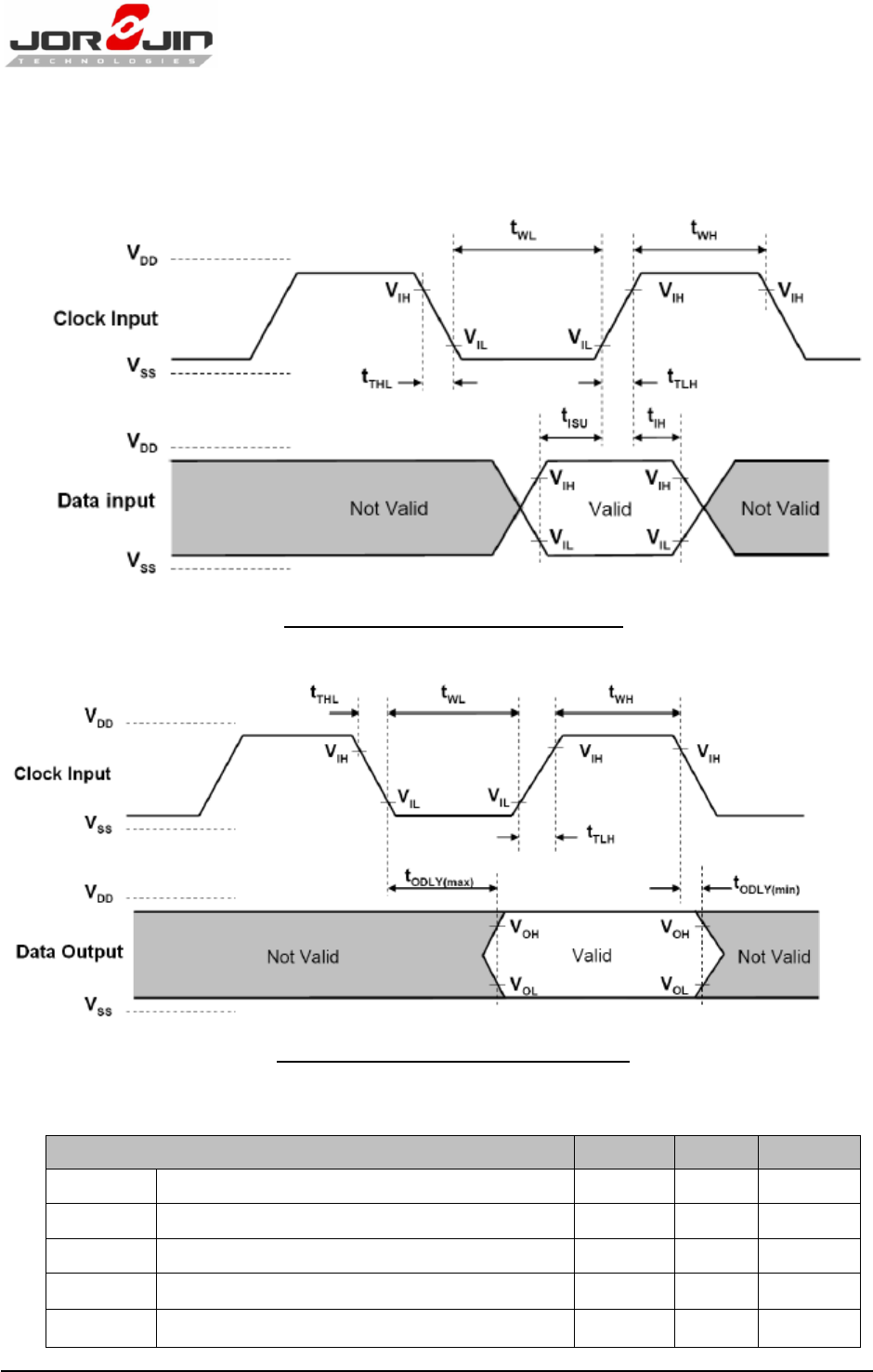
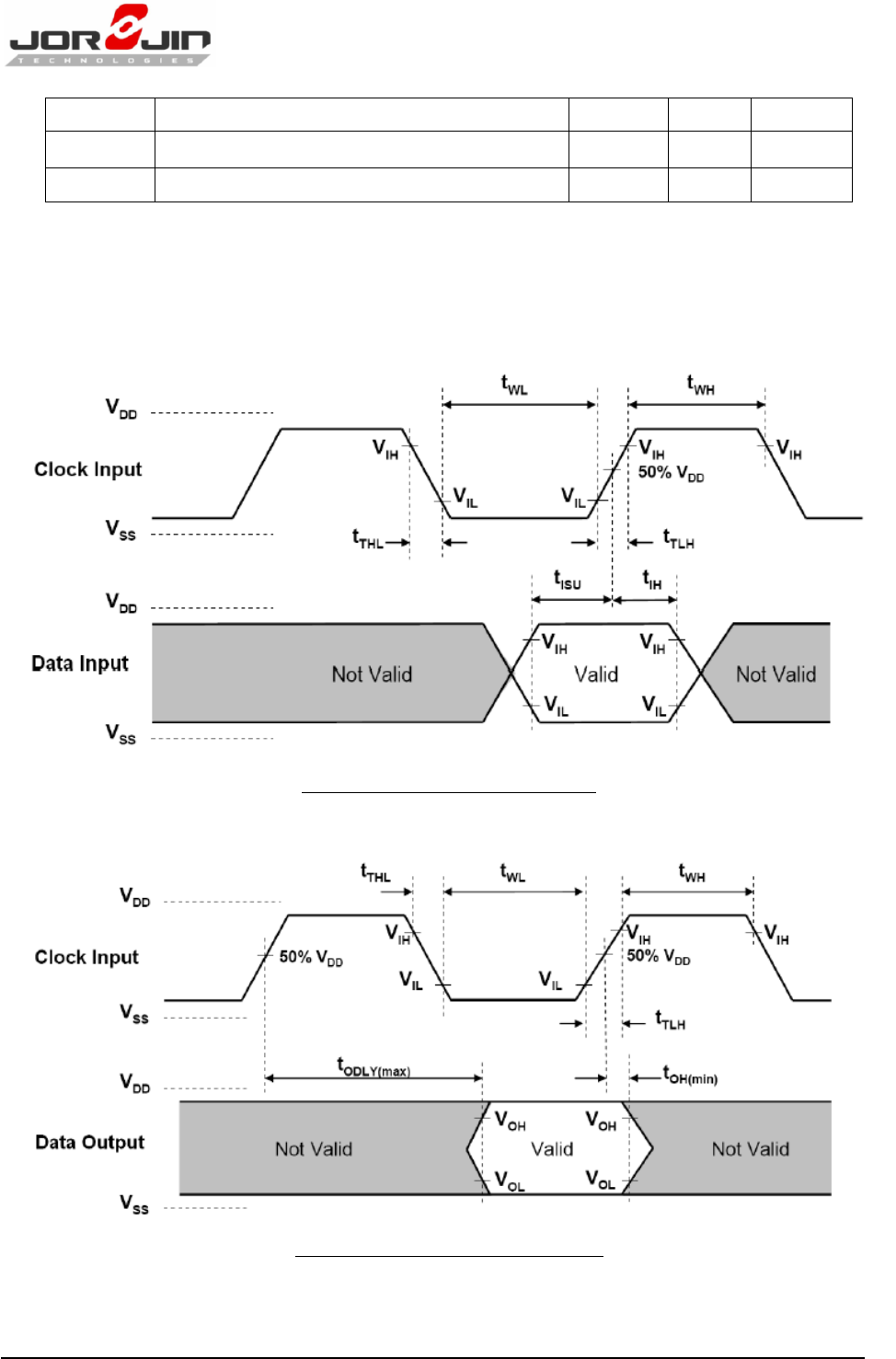
5.2. SDIO Timing Specifications
5.2.1. SDIO Switching Characteristics – Default Rate
Figure 5-1. SDIO default input timing
Figure 5-2. SDIO default output timing
Table 5-1. SDIO Default Timing Characteristics
(1)
PARAMETER
(2)
MIN MAX UNIT
Fclock Clock frequency, CLK 0 26 MHz
DC Low/high duty cycle 40 60 %
tTLH Rise time, CLK 10 ns
tTHL Fall time, CLK 10 ns
tISU Setup Ɵme, input valid before CLK↑ 3 ns
Doc No: WG7833-B0-DTS-R03
Copyright
©
JORJIN TECHNOLOGIES INC. 2015
http://WWW.JORJIN.COM.TW
CONFIDENTIAL
Page 34
tIH Hold Ɵme, input valid aŌer CLK↑ 2 ns
tODLY Delay Ɵme, CLK↓ to output valid 2.5 14.8 ns
CI Capacitive load on outputs 15 pF
(1) To change the data out clock edge from the falling edge (default) to the rising edge, set the configuration bit.
(2) Parameter values reflect maximum clock frequency.
5.2.2. SDIO Switching Characteristics – High Rate
Figure 5-3. SDIO HS input timing
Figure 5-4. SDIO HS output timing
Doc No: WG7833-B0-DTS-R03
Copyright
©
JORJIN TECHNOLOGIES INC. 2015
http://WWW.JORJIN.COM.TW
CONFIDENTIAL
Page 35
Table 5-2. SDIO HS Timing Characteristics
PARAMETER MIN MAX UNIT
Fclock Clock frequency, CLK 0 50 MHz
DC Low/high duty cycle 40 60 %
tTLH Rise time, CLK 3 ns
tTHL Fall time, CLK 3 ns
tISU Setup Ɵme, input valid before CLK↑ 3 ns
tIH Hold Ɵme, input valid aŌer CLK↑ 2 ns
tODLY Delay Ɵme, CLK↓ to output valid 2.5 14 ns
CI Capacitive load on outputs 10 pF
5.3. HCI UART Shared Transport Layers for All Functional Blocks (Except WLAN)
The HCI UART supports most baud rates (including all PC rates) for all fast clock frequencies - up
to a maximum of 4 Mbps. After power up the baud rate is set for 115.2 kbps, regardless of fast
clock frequency. The baud rate can then be changed by using a VS command. The Device
responds with a Command Complete Event (still at 115.2 kbps), after which the baud rate change
occurs.
HCI hardware includes the following features:
Receiver detection of break, idle, framing, FIFO overflow and parity error conditions.
Receiver Transmitter underflow detection.
CTS/RTS hardware flow control.
4 wires (H4)
The below table lists the UART default settings
Table 5-3. UART Default Setting
Parameter Value
Bit Rate 115.2 kbps
Data Length 8 bits
Stop Bit 1
Parity None
Doc No: WG7833-B0-DTS-R03
Copyright
©
JORJIN TECHNOLOGIES INC. 2015
http://WWW.JORJIN.COM.TW
CONFIDENTIAL
Page 36
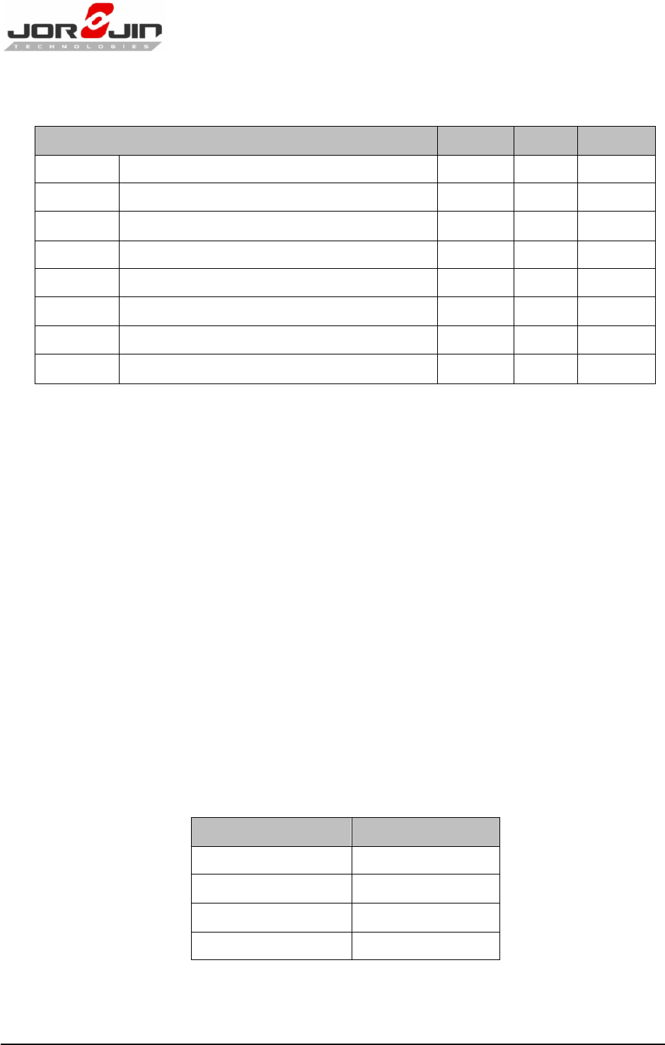
5.3.1. UART 4-Wires Interface – H4
The interface includes four signals: TXD, RXD, CTS and RTS. Flow control between the host and
the Device is byte-wise by hardware. ( See Figure 5-5 )
Figure 5-5. HCI UART Connection
When the UART RX buffer of the device passes the flow-control threshold, the buffer sets the
UART_RTS signal high to stop transmission from the host. When the UART_CTS signal is set high,
the device stops transmitting on the interface. If HCI_CTS is set high in the middle of transmitting
a byte, the device finishes transmitting the byte and stops the transmission.
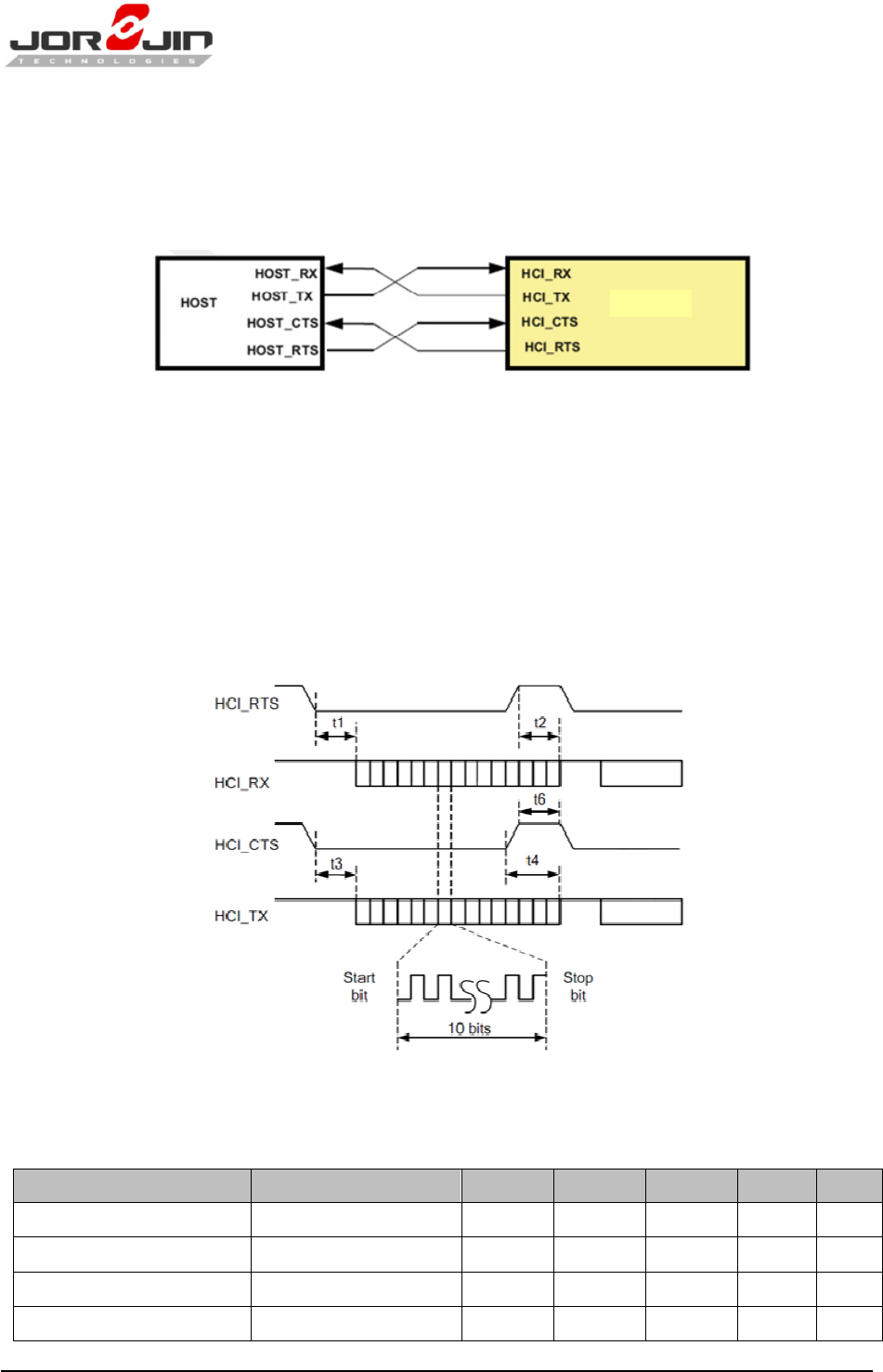
5.4. UART Timing Specifications
Figure 5-6. UART Timing Diagram
Table 5-4. UART Timing Characteristics
Characteristic Condition Symbol Min Typ Max Unit
Baud rate 37.5 4364 Kbps
Baud rate accuracy per byte
RX/TX -2.5 +1.5 %
Baud rate accuracy per bit RX/TX -12.5 +12.5 %
CTS low to TX_DATA on t3 0 2 us
Doc No: WG7833-B0-DTS-R03
Copyright
©
JORJIN TECHNOLOGIES INC. 2015
http://WWW.JORJIN.COM.TW
CONFIDENTIAL
Page 37
CTS low to TX_DATA off Hardware flow control t4 1 Byte
CTS High Pulse Width t6 1 bit
RTS low to RX_DATA on t1 0 2 us
RTS high to RX_DATA off Interrupt set to 1/4 FIFO
t2 16 Bytes
STR-Start bit; D0..Dn - Data bits (LSB first); PAR - Parity bit (if used); STP - Stop bit
Figure 5-7. UART Data Frame
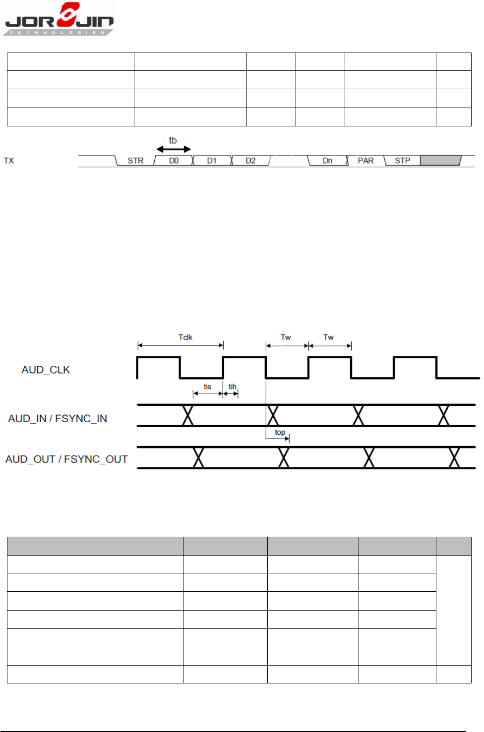
5.5. Bluetooth Codec-PCM(Audio) Timing Specifications
Figure 5-8 shows the Bluetooth codec-PCM (audio) timing diagram.
Table 5-5 lists the Bluetooth codec-PCM master timing characteristics.
Table 5-6 lists the Bluetooth codec-PCM slave timing characteristics.
Figure 5-8. PCM Interface Timing
Table 5-5. Bluetooth Codec-PCM Master Timing Characteristics
Parameter Symbol Min Max Unit
Cycle time Tclk 166.67 (6.144MHz)
15625 (64 kHz)
ns
High or low pulse width Tw 35% of Tclk min
AUD_IN setup time tis 10.6
AUD_IN hold time tih 0
AUD_OUT propagation time top 0 15
AUD_FSYNC_OUT propagation time top 0 15
Capacitive loading on outputs Cl 40 pF

Doc No: WG7833-B0-DTS-R03
Copyright
©
JORJIN TECHNOLOGIES INC. 2015
http://WWW.JORJIN.COM.TW
CONFIDENTIAL
Page 38
Table 5-6. Bluetooth Codec-PCM Slave Timing Characteristics
Parameter Symbol Min Max Unit
Cycle time Tclk 81 (12.288MHz) ns
High or low pulse width Tw 35% of Tclk min
AUD_IN setup time tis 5
AUD_IN hold time tih 0
AUD_OUT propagation time top 5
AUD_FSYNC_OUT propagation time top 0 19
Capacitive loading on outputs Cl 40 pF
Doc No: WG7833-B0-DTS-R03
Copyright
©
JORJIN TECHNOLOGIES INC. 2015
http://WWW.JORJIN.COM.TW
CONFIDENTIAL
Page 39
6. CLOCK AND POWER MANAGEMENT
The slow clock is a free-running, 32.768 kHz clock supplied from an external clock source. The
clock is connected to the RTC_CLK pin and is a digital square-wave signal in the range of 0 to 1.8V
nominal
6.1. Reset-Power-Up System
After VBAT and VIO are fed to the device and while BT_EN and WL_EN are deasserted (low), the
device is in SHUTDOWN state, during which functional blocks, internal DC-DCs, and LDOs are
disabled. The power supplied to the functional blocks is cut off. When one of the signals (BT_EN
or WL_EN) are asserted (high), a power-on reset (POR) is performed. Stable slow clock, VIO, and
VBAT are prerequisites for a successful POR.
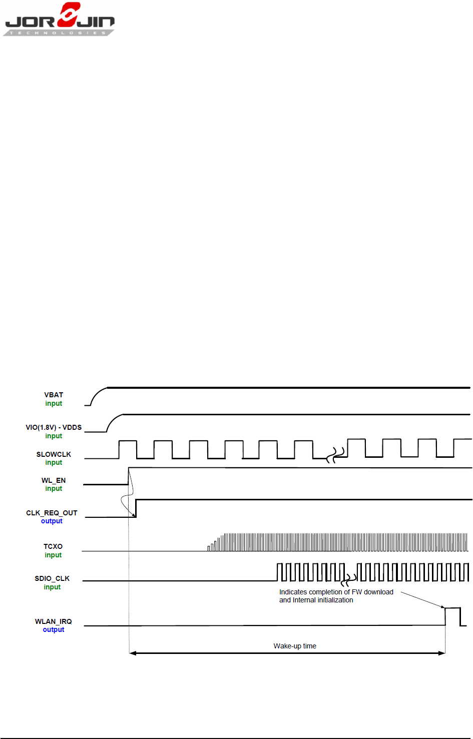
6.2. WLAN Power-Up Sequence
Figure 6-1 shows the WLAN power-up sequence.
Figure 6-1. WLAN Power-Up Sequence
Doc No: WG7833-B0-DTS-R03
Copyright
©
JORJIN TECHNOLOGIES INC. 2015
http://WWW.JORJIN.COM.TW
CONFIDENTIAL
Page 40
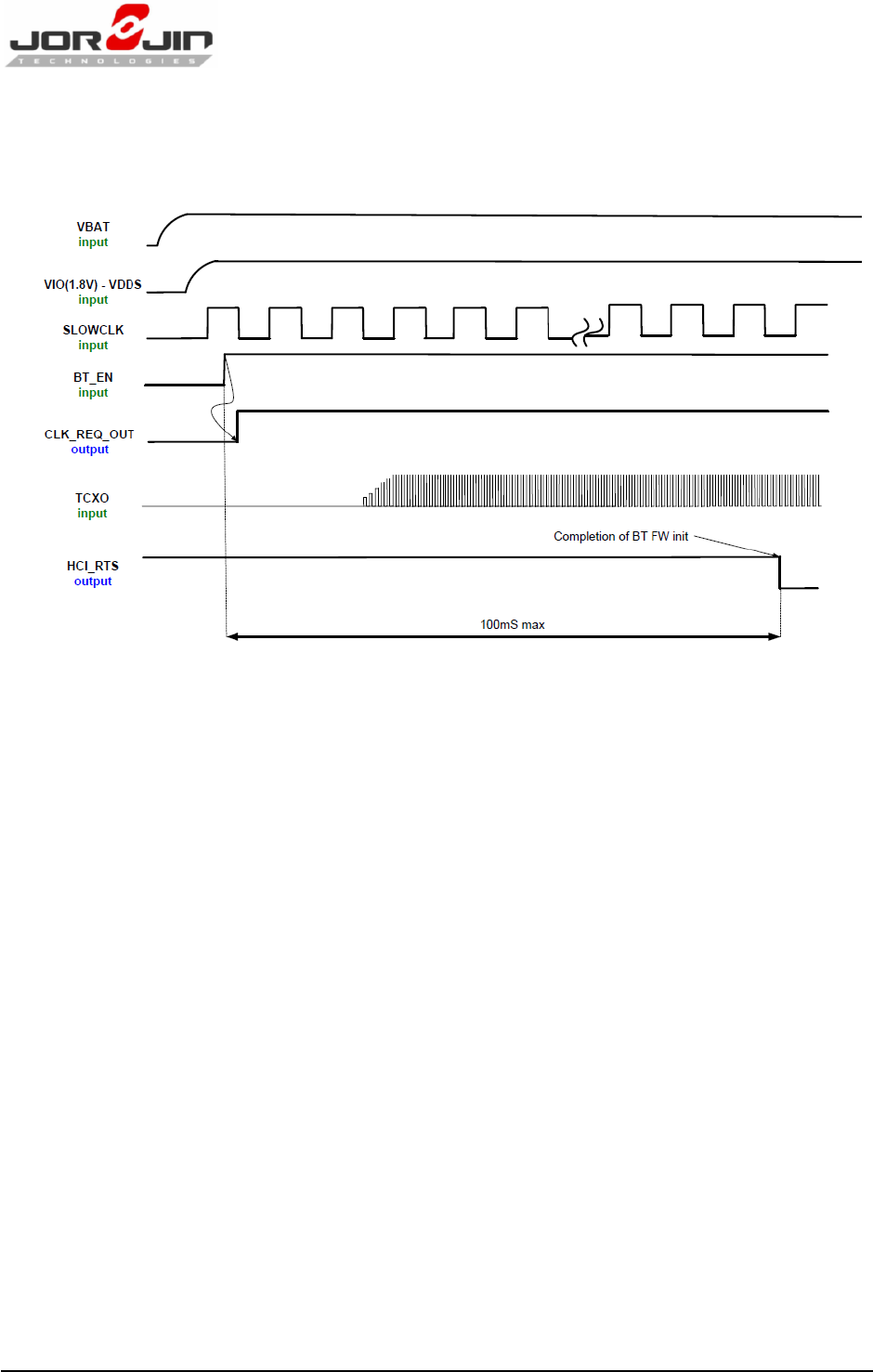
6.3. Bluetooth/BLE/ANT Power-Up Sequence
Figure 6-2 shows the Bluetooth/BLE/ANT power-up sequence.
Figure 6-2 Bluetooth/BLE/ANT power-up sequence
Doc No: WG7833-B0-DTS-R03
Copyright
©
JORJIN TECHNOLOGIES INC. 2015
http://WWW.JORJIN.COM.TW
CONFIDENTIAL
Page 41
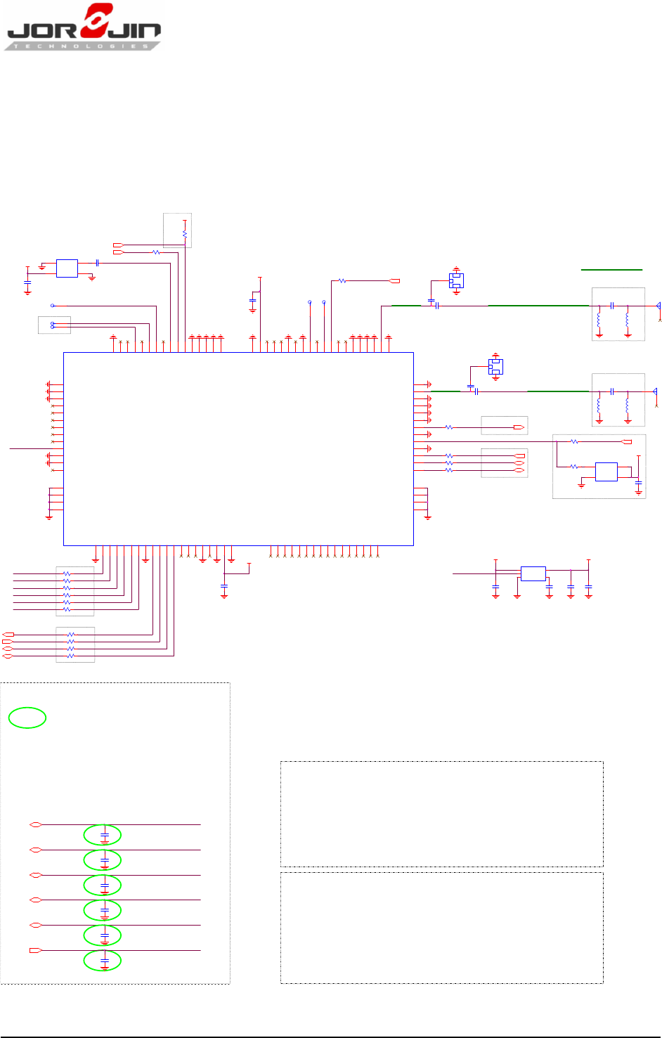
7. REFERENCE SCHEMATIC
7.1. Module Reference Design
BT_EN_1V8
R3 0R RES1005
VIO_IN
WLAN_I RQ_1V8
R1
NL_10K
RES1005
TC XO_CLK_IN
C4
1uF
CAP1005
For RTTT test
VBAT_IN
EXT_32K
TCXO1
TCXO/2016/26MHz
TCXO-2.0X1.6
GND
1
VCC
4
OUT 3
GND 2
C1
33pF
CAP1005
U1
WG7833_03_31_01-B0 D01 Module
E-12X12.8-0.6-TOP
GND C13
GND C14
GND C15
GND C16
NL
B16
NL
B15
NL
B14
NL
B13
NL
B12
NL
B11
NL
B10
NL
B9
NL
B8
NL
B7
GP1O12
B6
GPIO10
B5
GPIO9
B4
GPIO11
B3
NL
J9
NL
J8
NL
B2
NL
B1
CLK_REQ_OUT
J10
NL
J13
NL
J7
NL
J6
NL
J5
NL
J4
GND
J11
GND
J12
GND
J3
VBAT_IN D2
GND
J1
GND
A1
WL_SDI O_D3
A2
WL_SDI O_CMD
A3
WL_SDI O_D2
A4
WL_SDI O_D0
A5
WL_SDI O_D1
A6
WL_SDI O_CLK
A7
GND
A8
BT_HCI _RX
A12
BT_HCI _RT S
A10
BT_HCI _CT S
A9
NL
A15
GND
A16
NL
A17
GND
A18
BT_AUD_FSY NC K13
BT_AUD_CLK K12
BT_AUD_IN K11
GND K10
SLOW_CLK K9
GND K8
GND K3
GND K6
BT_AUD_OUT K7
GND K4
GND K5
RF _ANT_BG K2
GND K1
GND D20
GND D15
NL D5
GND D6
PA_DC2 DC_OU T D9
GND D8
NL D14
GPIO_4 D10
BT_EN D12
GND
J2
RF_ANT _A D19
GND D16
GND D17
GND D18
GND C12
WLAN _IRQ C11
WLAN_EN C10
TCXO_CLK_IN C9
NL C8
GPIO3_WL_U ART_D BG C6
NL D7
NL C5
BT_UART_DEBUG C4
NL C3
NL C2
GND C1
GND
E1
GND
E2
GND
E3
GND
E4 GND F4
GND F 3
NL
A13
NL
A14
NL D13
GPIO_2/ WL_RS232_RX D11
NL D4
NL D3
GPIO1/WL_232_TX C7
GND D1
GND F 2
GND F 1
VIO_IN
A19
GND
A20
BT_HCI _TX
A11
WL/BT_2.4G ANT
L3
NL
IND 1005
C11
10pF
CAP1005
C10
NL_10pF
CAP1005
C12
10pF
CAP1005
Reserved for RF test.
Closed to Module.
L4
NL
IND 1005
Pi-Circuit for Antenna matching.
ANT2
1
2
CLK_REQ_OUT_1833
TP9 1WL_RS232_TX
VDD _TCXO_OUT
U2
SOT-23-5
TPS73618DBV
IN
1
GND
2EN
3
NR/ FB 4
OUT 5
C18
0.1uF
CAP1005
C19
10uF
CAP2012
C20
0.1uF
CAP1005
C22
10nF
CAP1005
VBAT_IN
WL_5G ANT (For WG7833/03 Only)
L1
NL
IND 1005
C5
NL_10pF
CAP1005 C3
10pF
CAP1005
Reserved for RF test.
Closed to Module.
C6
10pF
CAP1005
L2
NL
IND 1005
VDD_TCXO_OUT
ANT1
1
2
Pi-Circuit for Antenna matching.
CLK_REQ_OUT_1833
R22 0R RES1005
R19 0R RES1005
For BT (WG7833/31)
BD_HC I_TX_1V8
BD_HC I_RX_1V8
BD_HC I_CTS_1V8
R21 0R RES1005
R20 0R RES1005
R7 0R RES1005 BT_PCM_AUD_I N
BT_PCM_AUD _CLK
R8 0R RES1005
R10 0R RES1005 BT_PCM_AUD_FSYN C
Must reserve PU cricuit
for Debug.
C2
0.1uF
CAP1005
BT_PCM_AUD _OUT
R4 0R RES1005
C16
0.1uF
CAP1005
OSC1
OSC/3 225/32.768kHz
EN 1
VCC 4
OUT
3
GND
2
R9
0R
RES1005
32.768KHz source select
VIO_IN
TP3
1
50 ohms single ended
ANTENNA CIRCUITS
TP4
1
WL_RS232_R X
J2
U. FL-R-SMT-1(10)
U. FL
1
2 3
HOST_SLOWCLK_1V8
R5
0R
RES1005
C17
0.1uF
CAP1005
VIO_IN
WL_EN_1V8 R2 0R
RES1005
For BT (WG7833/31)
R11 0R RES1005
R15 0R RES1005
R12 0R RES1005
R18 0R RES1005
R14 0R RES1005
SDIO_D 3_1V8
R16 0R RES1005
SDIO_C LK_1V8
SDIO_D 0_1V8
SDIO_D 2_1V8
SDIO_C MD_1V8
SDIO_D 1_1V8
For BT (WG7833/31)
TP1 1
TP2 1
For Logger
J1
U.F L-R-SMT-1(10)
U.F L
1
2 3
BD_HC I_RTS_1V8
C9
NL
CAP1005
C13
NL
CAP1005
C7
NL
CAP1005
C8
NL
CAP1005
C15
NL
CAP1005
C14
NL
CAP1005
** The six traces from Module to Host must be
treated like a bus. The bus length shall be as short
as possible and every trace length must be the same as
the others. Enough space above 2 time trace width or
ground shielding between trace and trace will be benefit
to make sure signal quality, especially for SDIO_CLK
trace. Besides, please remember to keep them away from
the other digital or analog signal traces. To add ground
shielding to around the buses will be helpful.
** It's recommended to reserve SDID matching circuits
and keep them close to module for signal optimization
WiFi SDIO Matching Circuit
SDIO_D1_1V8
SDIO_CLK_1V8
SDIO_D3_1V8
SDIO_D2_1V8
** All test point must reserved for test
SDIO_CMD_1V8
SDIO_D0_1V8
In green circle is a necessary part
** SDIO lines should be held high by the host
Boot Conditions
Scheme Brief
WiFi Interface: SDIO
Slow Clock: 32.768KHz for module boot
and deep sleep
VIO_IN: 1.62~1.95V => 1.8V TYP
VBAT_IN: 2.9~4.8V => 3.7V TYP
Fast Clock:
External TCXO 26MHz
Slow Clock: 32.768KHz
Figure 7-1 Module Reference Schematic

Doc No: WG7833-B0-DTS-R03
Copyright
©
JORJIN TECHNOLOGIES INC. 2015
http://WWW.JORJIN.COM.TW
CONFIDENTIAL
Page 42
8. DESIGN RECOMMENDATIONS
8.1. Design Note on Debug Port
Pin# C6, C4 serve as WLAN and BT debug port, respectively. So test points for these two
signals should be reserved for debugging purpose.
Pin# C11 (WLAN_IRQ) needs to be pulled high via 10Kohm and use Pin# D11, C7
(WL_RS232_RX, WL_RS232_TX) as hardware interface to communicate with system platform
and TI RTTT test utility for WLAN RF performance test, debug and manufacturing application.
8.2. Module Layout Recommendations
Follow these module layout recommendations:
Digital Signals Layout
SDIO signals traces (CMD, D0, D1, D2 and D3) should be routed in parallel to each other and
as short as possible. (Less than 12cm) Besides, every trace length must be the same as the
others.
Enough space above 1.5 time trace width or ground shielding between trace and trace will
be benefit to make sure signal quality, especially for SDIO_CLK trace. Remember to keep
them away from the other digital or analog signal traces. Adding ground shielding around
these bus is recommended.
Route trace of SDIO_CLK at Top layer without vias.
SDIO Clock, Audio Clock (PCM_AUD_CLK), these digital clock signals are a source of noise.
Keep the traces of these signals as short as possible. Whenever possible, maintain a
clearance around them.
BT_AUD signals should be rounted in the same group and it’s better to rout them at the
same layer or confirm them referring to the same reference plane.
RF Trace & Antenna
Keep 50ohm trace impedance.
Move all the high-speed traces and components far away from the antenna.
Check antenna vendor for the layout guideline and clearance.
Power Trace
Power trace for VBAT should be 20mil wide. 1.8V trace should be 15mil wide, at least.

Doc No: WG7833-B0-DTS-R03
Copyright
©
JORJIN TECHNOLOGIES INC. 2015
http://WWW.JORJIN.COM.TW
CONFIDENTIAL
Page 43
Isolate different power traces with Ground plane
Ground
Having a complete Ground and more GND vias under module in layer1 for system stable
and thermal dissipation.
Have a complete Ground pour in layer 2 for thermal dissipation.
Increase the GND pour in the 1st layer, move all the traces from the 1st layer to the inner
layers if possible.
Move GND vias close to the pad.
Clocks
To avoid adding noise to the clock signal, keep the primary clock away from fast digital
switching lines and power traces.
It is preferable to keep all clocks between the ground/power layers.
Primary TCXO placement
- To reduce clock drift, place the TCXO far from a heat source on the board.
- For better thermal mass, ensure good grounding for the TCXO.
- If the TCXO cannot be placed far from a heat source, add a scratch in the ground layers to
isolate the heat spreading toward the TCXO
Primary TCXO placement:
To reduce clock drift, place the TCXO far from a heat source on the board.
For better thermal mass, ensure good grounding for the TCXO.
If the TCXO cannot be placed far from a heat source, add a scratch in the ground layers
to isolate the heat spreading toward the TCXO
Doc No: WG7833-B0-DTS-R03
Copyright
©
JORJIN TECHNOLOGIES INC. 2015
http://WWW.JORJIN.COM.TW
CONFIDENTIAL
Page 44
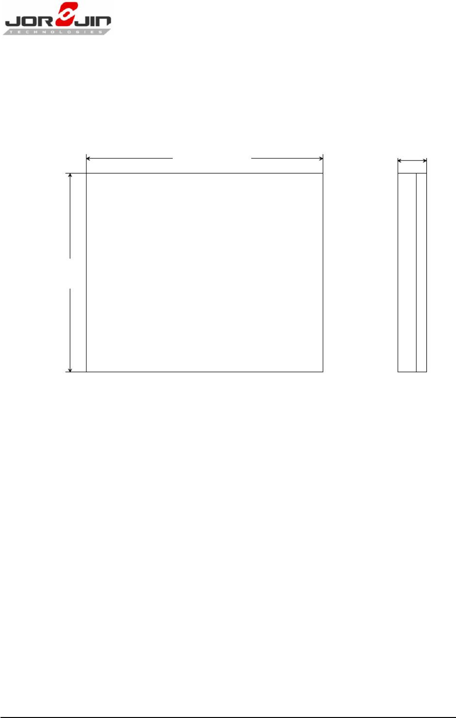
9. PACKAGE INFORMATION
9.1. Module Mechanical Outline
Figure 9-1. Module mechanical outline
12.0±0.1 mm
12.8±0.1 mm 1.63±0.1 mm
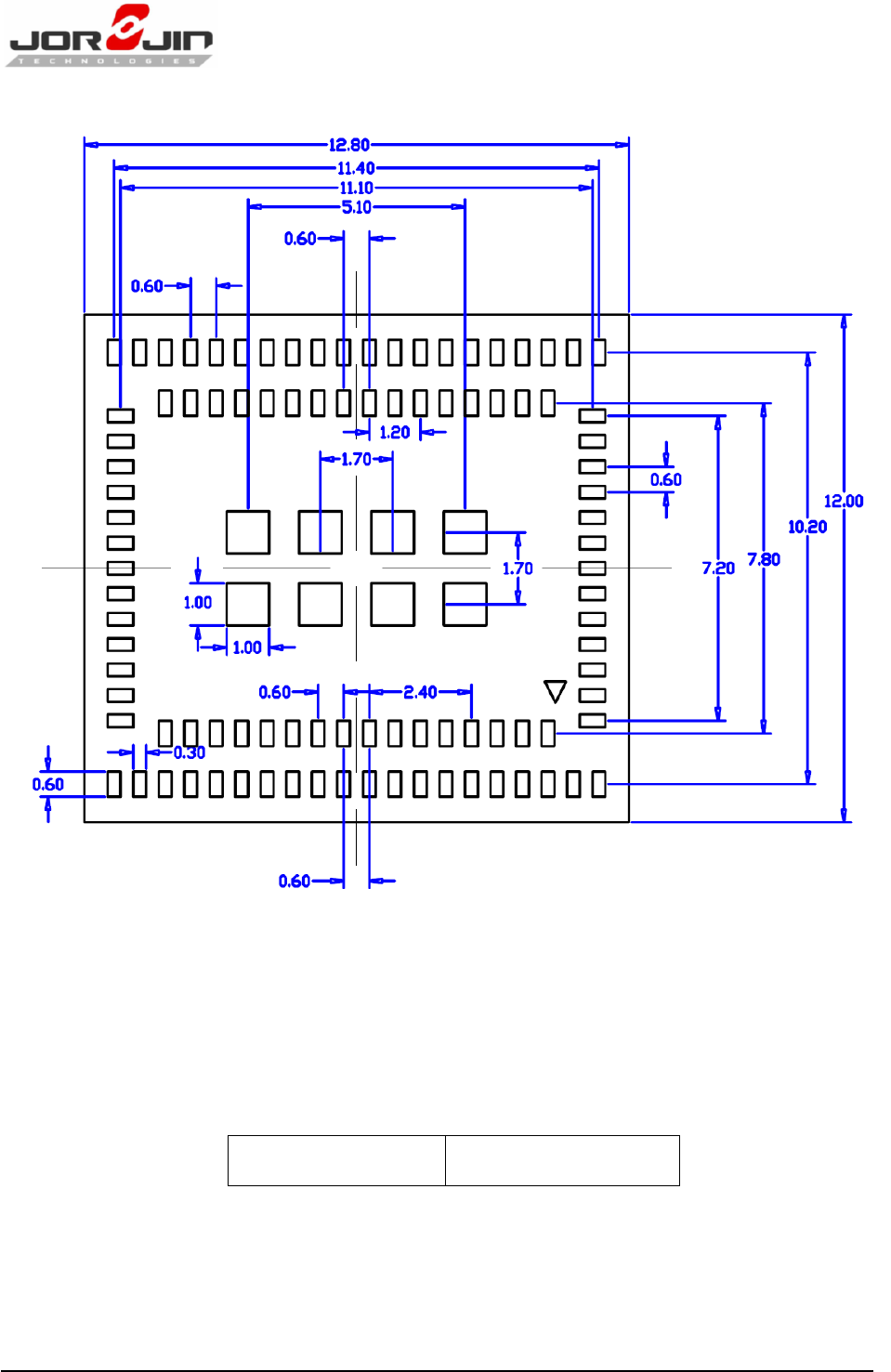
Doc No: WG7833-B0-DTS-R03
Copyright
©
JORJIN TECHNOLOGIES INC. 2015
http://WWW.JORJIN.COM.TW
CONFIDENTIAL
Page 45
Figure 9-2. Module pad dimensions
*We recommend adopting the same dimensions listed above for building PCB footprint.
** Pad tolerance as +/- 30um
9.2. Ordering Information
Part number: WG7833-B0
Doc No: WG7833-B0-DTS-R03
Copyright
©
JORJIN TECHNOLOGIES INC. 2015
http://WWW.JORJIN.COM.TW
CONFIDENTIAL
Page 46
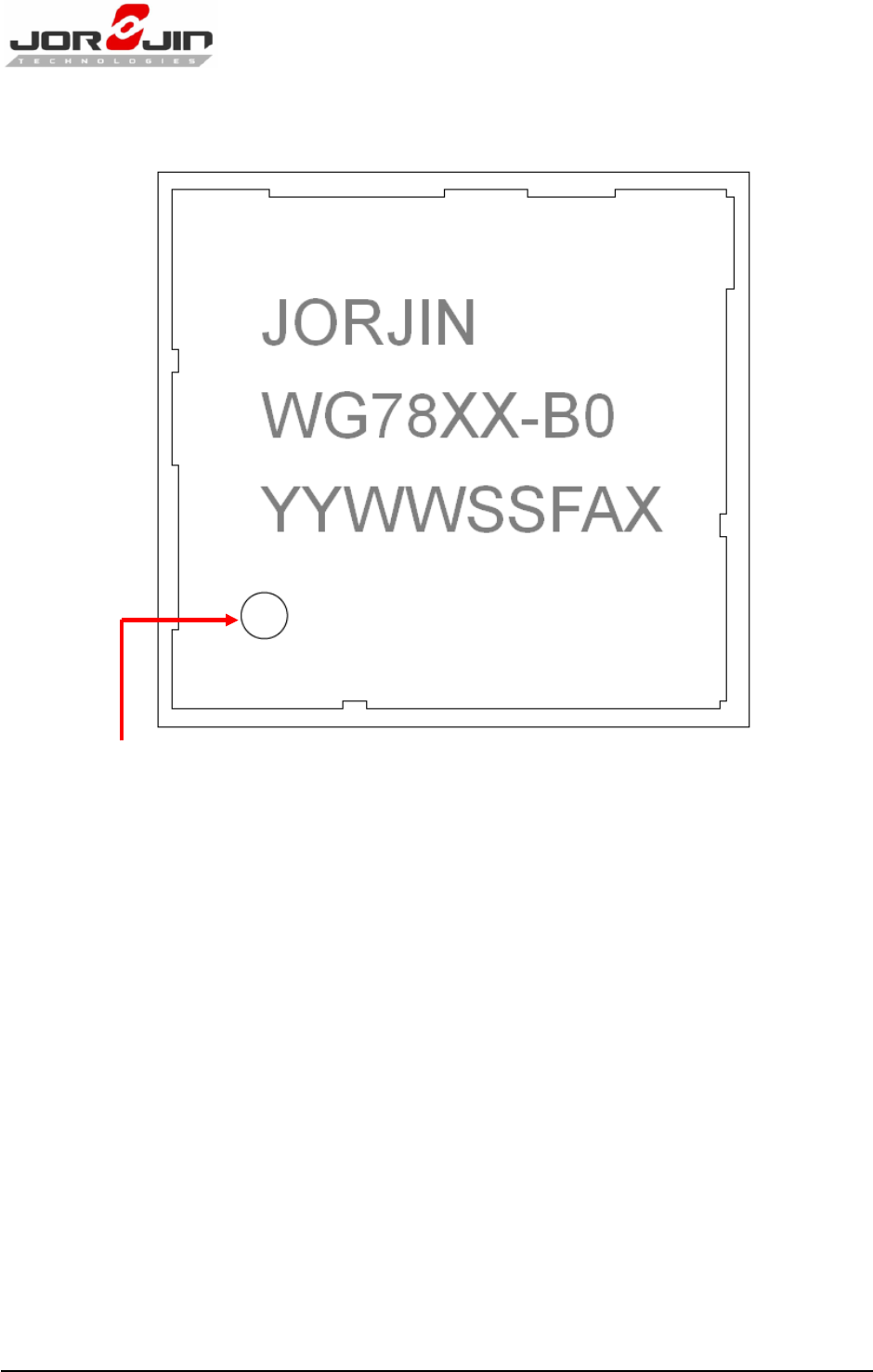
9.3. Package Marking
Figure 9-3. Package Marking
Date Code: YYWWSSFAX
YY = Digit of the year, ex: 2011=11
WW = Week (01~52)
SS = Serial number from 01 ~99 match to manufacture’s lot number
F = Reserve for internal use
A = Module version from A to Z
X = Chip version
PIN-1 Marking
Doc No: WG7833-B0-DTS-R03
Copyright
©
JORJIN TECHNOLOGIES INC. 2015
http://WWW.JORJIN.COM.TW
CONFIDENTIAL
Page 47
9.4. Packaging
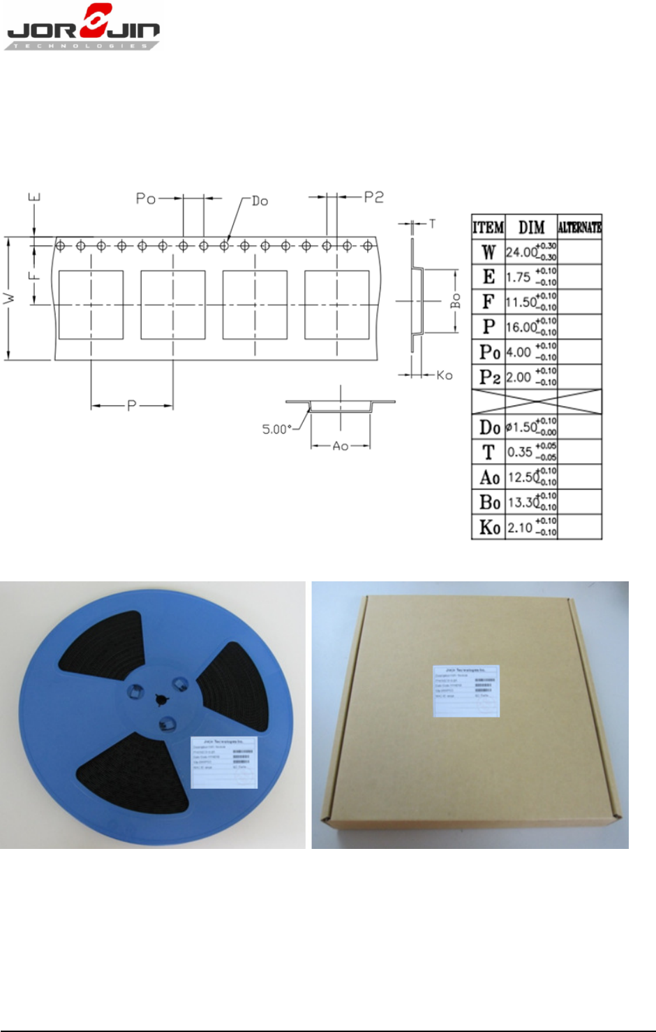
9.4.1. Tape Specification
<Reel : 1.8K pcs per reel> <Pizza box : 1 reel per pizza box>
Doc No: WG7833-B0-DTS-R03
Copyright
©
JORJIN TECHNOLOGIES INC. 2015
http://WWW.JORJIN.COM.TW
CONFIDENTIAL
Page 48
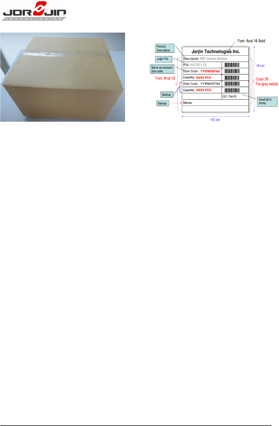
<Carton : 5 pizza boxes per carton> Product label
Doc No: WG7833-B0-DTS-R03
Copyright
©
JORJIN TECHNOLOGIES INC. 2015
http://WWW.JORJIN.COM.TW
CONFIDENTIAL
Page 49
10. SMT AND BAKING RECOMMENDATION
10.1. Baking Recommendation
Baking condition:
- Follow MSL Level 4 to do baking process.
- After bag is opened, devices that will be subjected to reflow solder or other high
temperature process must be
a) Mounted within 72 hours of factory conditions <30°C/60% RH, or
b) Stored at <10% RH.
- Devices require bake, before mounting, if Humidity Indicator Card reads >10%
If baking is required, Devices may be baked for 8 hrs. at 125 °C.
10.2. SMT Recommendation
Recommended Reflow profile:
No. Item Temperature (°C) Time (sec)
1 Pre-heat D1: 140 ~ D2: 200 T1: 80 ~ 120
2 Soldering D2: = 220 T2: 60 +/- 10
3 Peak-Temp. D3: 250 °C max
H
Doc No: WG7833-B0-DTS-R03
Copyright
©
JORJIN TECHNOLOGIES INC. 2015
http://WWW.JORJIN.COM.TW
CONFIDENTIAL
Page 50
Note: (1) Reflow soldering is recommended two times maximum.
(2) Add Nitrogen while Reflow process: SMT solder ability will be better.
Stencil thickness:
::
: 0.1~ 0.13 mm (Recommended)
Soldering paste (without Pb):
::
: Recommended SENJU N705-GRN3360-K2-V can get better
soldering effects.
11. HISTORY CHANGE
Revision Date Description
R 0.1 2014/08/28 New Released
R 0.2 2014/09/29 Modify the module thickness from 1.7±0.05 mm to 1.63±0.1 mm
Modify the package marking.
R 0.3 2015/07/30 Add FCC/NCC WARING STATEMENT

Doc No: WG7833-B0-DTS-R03
Copyright
©
JORJIN TECHNOLOGIES INC. 2015
http://WWW.JORJIN.COM.TW
CONFIDENTIAL
Page 51
FCC WARING STATEMENT
This equipment has been tested and found to comply with the limits for a Class B digital device,
pursuant to part 15 of the FCC rules. These limits are designed to provide reasonable protection
against harmful interference in a residential installation. This equipment generates, uses and can
radiate radio frequency energy and, if not installed and used in accordance with the instructions,
may cause harmful interference to radio communications. However, there is no guarantee that
interference will not occur in a particular installation. If this equipment does cause harmful
interference to radio or television reception, which can be determined by turning the equipment off
and on, the user is encouraged to try to correct the interference by one or more of the following
measures:
-Reorient or relocate the receiving antenna.
-Increase the separation between the equipment and receiver.
-Connect the equipment into an outlet on a circuit different from that to which the receiver is
connected.
-Consult the dealer or an experienced radio/TV technician for help.
You are cautioned that changes or modifications not expressly approved by the party responsible for
compliance could void your authority to operate the equipment.
This device complies with Part 15 of the FCC Rules. Operation is subject to the following two
conditions: (1) this device may not cause harmful interference and (2) this device must accept any
interference received, including interference that may cause undesired operation.
FCC RF Radiation Exposure Statement:
1. This Transmitter must not be co-located or operating in conjunction with any other antenna or
transmitter.
2. This equipment complies with FCC RF radiation exposure limits set forth for an uncontrolled
environment. This equipment should be installed and operated with a minimum distance of 20
centimeters between the radiator and your body.
According to FCC 15.407(e), the device is intended to operate in the frequency band of 5.15GHz to
5.25GHz under all conditions of normal operation. Normal operation of this device is restricted to
indoor used only to reduce any potential for harmful interference to co-channel MSS operations.
Information to OEM integrator
The OEM integrator has to be aware not to provide information to the end user regarding how to

Doc No: WG7833-B0-DTS-R03
Copyright
©
JORJIN TECHNOLOGIES INC. 2015
http://WWW.JORJIN.COM.TW
CONFIDENTIAL
Page 52
install or remove this RF module in the user manual of the end product. The user manual which is
provided by OEM integrators for end users must include the following information in a prominent
location.
1. To comply with FCC RF exposure compliance requirements, the antenna used for this transmitter
must be installed to provide a separation distance of at least 20 cm from all persons and must not
be co- located or operating in conjunction with any other antenna or transmitter, except in
accordance with FCC multi-transmitter product transmitter product procedures.
2. Only those antennas with same type and lesser gain filed under this FCC ID number can be used
with this device.
3. The regulatory label on the final system must include the statement: “Contains FCC ID:
WS2-WG7833B0 “.
4. The final system integrator must ensure there is no instruction provided in the user manual or
customer documentation indicating how to install or remove the transmitter module except such
device has implemented two-ways authentication between module and the host system.
5. If the end product integrating this module is going to be operated in 5.15 ~5.25GHz frequency
range, the warning statement in the user manual of the end product should include the restriction
of operating this device in indoor could void the user’s authority to operate the equipment.

Doc No: WG7833-B0-DTS-R03
Copyright
©
JORJIN TECHNOLOGIES INC. 2015
http://WWW.JORJIN.COM.TW
CONFIDENTIAL
Page 53
NCC WARING STATEMENT
Article 12
Without permission, any company, firm or user
shall not alter the frequency, increase the
power, or change the characteristics and
functions of the original design of the
certified lower power frequency electric
machinery.
Article 14
The application of low power frequency electric
machineries shall not affect the navigation
safety nor interfere a legal communication, if
an interference is found, the service will be
suspended until improvement is made and the
interference no longer exists.